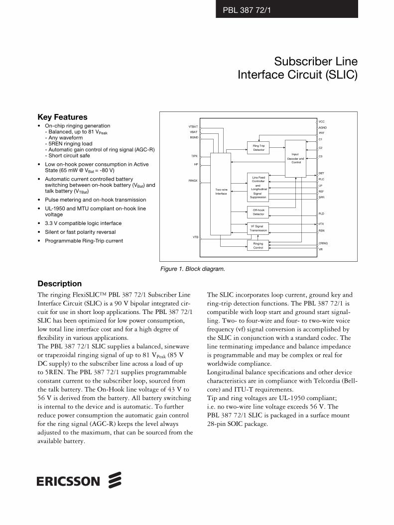
subscriber line interface circuit (slic)zoobab/bh.udev.org/filez/...block diagram. key features •...
TRANSCRIPT
REF
SPR
CRING
Ring Trip Detector
Input
Decoder and Control
Off-hook Detector
VF Signal Transmission
Two-wire Interface
VTBAT
C1
C2
C3
DET
PLC
LP
PLD
VTX
RSN
TIPX
HP
RINGX
BGND
Line Feed Controller
and Longitudinal
Signal Suppression
RingingControl
VR
VBAT
AGND
VCC
PRT
VTB
DescriptionThe ringing FlexiSLIC™ PBL 387 72/1 Subscriber Line Interface Circuit (SLIC) is a 90 V bipolar integrated cir-cuit for use in short loop applications. The PBL 387 72/1 SLIC has been optimized for low power consumption, low total line interface cost and for a high degree of flexibility in various applications.The PBL 387 72/1 SLIC supplies a balanced, sinewaveor trapezoidal ringing signal of up to 81 VPeak (85 V DC supply) to the subscriber line across a load of up to 5REN. The PBL 387 72/1 supplies programmable constant current to the subscriber loop, sourced from the talk battery. The On-Hook line voltage of 43 V to 56 V is derived from the battery. All battery switching is internal to the device and is automatic. To further reduce power consumption the automatic gain control for the ring signal (AGC-R) keeps the level always adjusted to the maximum, that can be sourced from the available battery.
Figure 1. Block diagram.
Key Features• On-chip ringing generation
- Balanced, up to 81 VPeak - Any waveform - 5REN ringing load - Automatic gain control of ring signal (AGC-R)- Short circuit safe
• Low on-hook power consumption in Active State (65 mW @ VBat = -80 V)
• Automatic current controlled battery switching between on-hook battery (VBat) and talk battery (VTBat)
• Pulse metering and on-hook transmission
• UL-1950 and MTU compliant on-hook line voltage
• 3.3 V compatible logic interface
• Silent or fast polarity reversal
• Programmable Ring-Trip current
Subscriber LineInterface Circuit (SLIC)
The SLIC incorporates loop current, ground key and ring-trip detection functions. The PBL 387 72/1 is compatible with loop start and ground start signal-ling. Two- to four-wire and four- to two-wire voice frequency (vf) signal conversion is accomplished by the SLIC in conjunction with a standard codec. The line terminating impedance and balance impedance is programmable and may be complex or real for worldwide compliance.Longitudinal balance specifications and other devicecharacteristics are in compliance with Telcordia (Bell-core) and ITU-T requirements.Tip and ring voltages are UL-1950 compliant; i.e. no two-wire line voltage exceeds 56 V. The PBL 387 72/1 SLIC is packaged in a surface mount 28-pin SOIC package.
PBL 387 72/1
PBL 387 72
2 EN/LZT 146 136 R1A ©Ericsson Microelectronics, December 2001
Maximum RatingsParameter Symbol Min Max Unit
Temperature, HumidityStorage temperature range TStg -55 +150 °C
Operating temperature range TAmb -40 +110 °C
Operating junction temperature range, Note 1 TJ -40 +140 °C
Power supply, -40°C ≤ TAmb ≤ +85°C
VCC with respect to AGND VCC -0.4 6.5 V
VTB with respect to AGND VTB VBat 0.4 V
VTBat with respect to A/BGND VTBat VBat 0.4 V
VBat with respect to BGND, continuous VBat -85 0.4 V
Power dissipationContinuous power dissipation at TAmb ≤ +85 °C PD 1.5 W
Peak power dissipation @ TAmb = +85 °C, t < 100 ms, tRep > 1 sec. PPD 4 W
GroundVoltage between AGND and BGND VG -5 VCC V
Digital inputs, outputs (C1, C2, C3, DET)
Input voltage VID -0.4 VCC V
Output voltage (DET not active) VOD -0.4 VCC V
Output current (DET) IOD 30 mA
Ring voltage, input (VR)
Input voltage VR -1.1 VCC V
TIPX and RINGX terminals, -40°C ≤ TAmb ≤ +85°C, VBat = -80 V
TIPX or RINGX current ITIPX, IRINGX -100 100 mA
TIPX or RINGX voltage, continuous (referenced to AGND) VTA, VRA VBat 2 V
TIPX or RINGX, pulse < 10 ms, tRep > 10 s, Note 2, Note 3 VTA, VRA VBat –15 5 V
TIPX or RINGX, pulse < 1 µs, tRep > 10 s, Note 2, Note 3 VTA, VRA VBat –20 10 V
TIP or RING, pulse < 250 ns, tRep > 10 s, Note 2 , Note 3 VTA, VRA VBat –25 15 V
Notes, Maximum Ratings1. The circuit includes thermal protection. Operation above max. junction temperature may degrade device reliability.
2. With the diodes DB and DTB included, see figure 8.
3. RF1 and RF2 > 20 Ω is also required. Pulse is supplied to RING and TIP outside RF1 and RF2.
4. The voltage of VTB sets the maximum line length see figure 12. The diode DTB is required see figure 8.
Recommended Operating ConditionParameter Symbol Min Max Unit
Ambient temperature TAmb -40 +85 °C
VCC with respect to AGND VCC 4.75 5.25 V
VTB with respect to A/BGND ,Note 4 VTB -32 -10 V
VBat with respect to BGND VBat -80 V
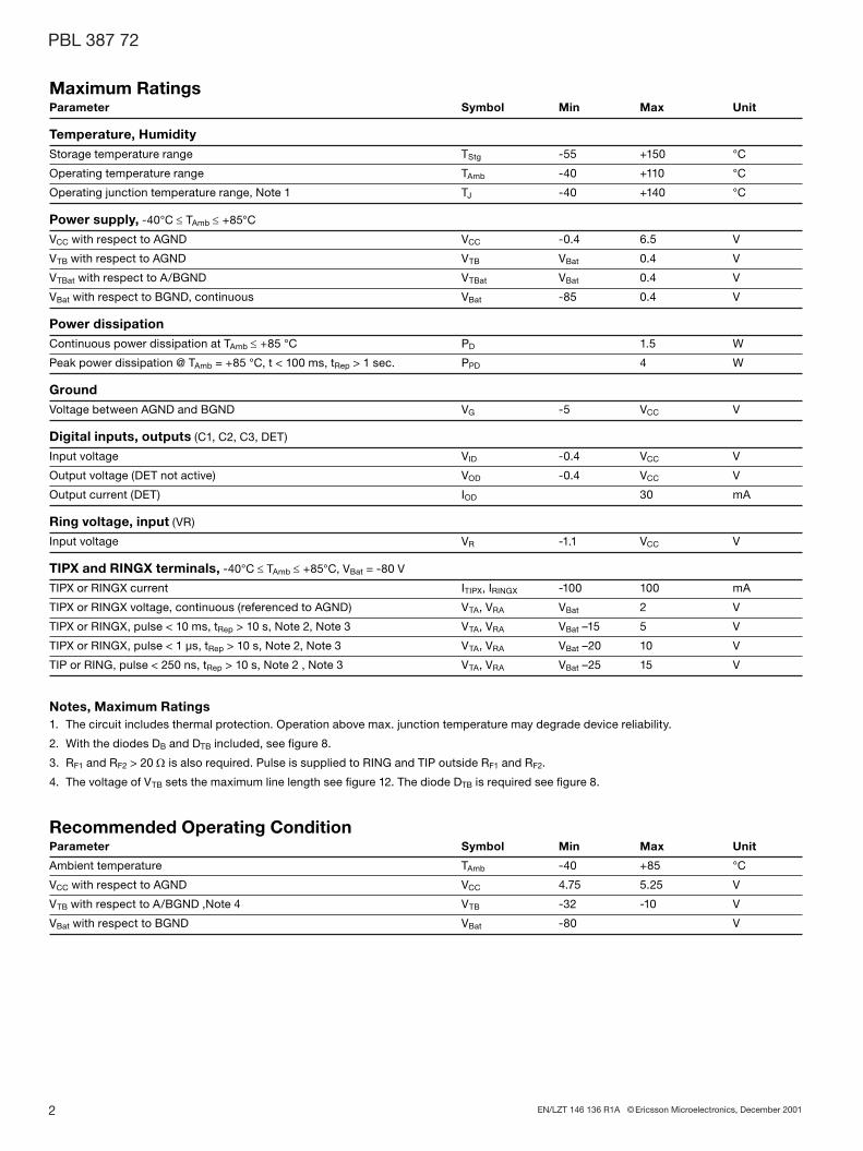
Electrical Characteristics-40 °C ≤ TAmb ≤ +85 °C, VCC = +5 V ±5 %, VTBat = -32 V to -10 V, VBat = -80 V, VR = 0.81 Vpk, RLC= 18.7 kΩ, (IL = 26.8 mA), ZL = 600 Ω, RLD = 49.9 kΩ, RF1 = RF2 = 0 , RRef = 15.0 kΩ, RRT = 66.5 kΩ, CHP = 33 nF, CLP= 0.47 µF, RT = 120 kΩ, RRX = 120 kΩ, RVR = 200 kΩ, CVR = 0.47 µF. Current definition: current is positive if flowing into a pin unless stated otherwise. Active state includes active normal and active reverse states unless otherwise specified.
Ref Parameter fig Conditions Min Typ Max Unit
Two-wire portOverload level, VTRO Active state Off-Hook, ILDC ≥ 10 mA 2 1% THD, Note 1 1.0 VPeak On-Hook, ILDC ≤ 5 mA 1.0 VPeak Metering, ILDC ≥ 10 mA ZLM = 200 Ω, f = 16 kHz 0.7 VPeak
Input impedance, ZTRX Note 2 ZT/200 Ω
Longitudinal impedance, ZLOT, ZLOR 0 < f < 100 Hz 20 35 Ω/wire
Longitudinal current limit, ILOT, ILOR active state 28 mArms /wire
Longitudinal to metallic balance, BLM IEEE standard 455-1985, ZTRX = 736 Ω 0.2 kHz < f < 1.0 kHz 53 70 dB 1.0 kHz < f < 3.4 kHz 53 70 dB
Longitudinal to metallic balance, BLME 3 active state ELO BLME = 20 × Log VTR 0.2 kHz ≤ f ≤ 1.0 kHz 53 70 dB 1.0 kHz < f < 3.4 kHz 53 70 dB
Longitudinal to four-wire balance, BLFE 3 active state ELO
BLFE = 20 × Log VTX 0.2 kHz ≤ f ≤ 1.0 kHz 53 70 dB 1.0 kHz < f < 3.4 kHz 53 70 dB
Metallic to longitudinal balance, BMLE 4 active state VTR BMLE = 20 × Log VLO , ERX = 0 0.2 kHz < f < 3.4 kHz 40 58 dB
PBL 387 72
TIPX
RINGX RSN
VTX
RT
RRX
ERXRL VTRO ILdc
C
PBL 387 72
TIPX
RINGX RSN
VTX
RT
RRX
VTX
RLTC
VTR
RLR
ELo
PBL 387 72
3 EN/LZT 146 136 R1A ©Ericsson Microelectronics, December 2001
1 << RL, RL= 600 ΩωC
RT = 120 kΩ, RRX = 120 kΩ
1 << 150 Ω, ωC
RLT = RLR = 300Ω or 368 Ω
RT = 120 kΩ, RRX = 120 kΩ
Figure 3. Longitudinal to metallic, BLME, and Longitudinal to four-wire, BLFE, balance.
Figure 2. Overload level, VTRO, two-wire port.
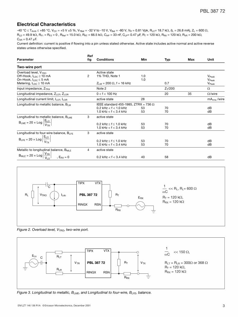
Ref Parameter fig Conditions Min Typ Max Unit
Four-wire to longitudinal balance, BFLE 4 active state 40 58 dB ERX BFLE = 20 × Log VLo 0.2 kHz < f < 3.4 kHz
Two-wire return loss, r |ZTRX + ZL| 0.2 kHz < f < 0.5 kHz 25 dB r = 20 × Log |ZTRX – ZL| 0.5 kHz < f < 1.0 kHz 27 dB 1.0 kHz < f < 3.4 kHz, Note 3 23 dB
TIPX idle voltage, VTI active normal, IL = 0 - 0.9 V
RINGX idle voltage, VRI active normal, IL = 0 - 51 V
Open loop voltage, |VTR Open| active, IL = 0 43 50 56 V
Four-wire transmit port (VTX)
Overload level, VTXO 5Off-hook, IL ≥ 10mA Load impedance > 20 kΩ, 0.5 VPeakOn-hook, IL ≤ 5mA Load impedance > 20 kΩ, 0.5 VPeak 1% THD, Note 4
Output offset voltage, ∆VTX -100 100 mV
Output impedance, ZTX 0.2 kHz < f < 3.4 kHz 5 20 Ω
Four-wire receive port (receive summing node = RSN)
RSN dc offset voltage, VRSNdc IRSN = 0 mA -25 25 mV
RSN impedance 0.2 kHz < f < 3.4 kHz 10 50 Ω
RSN current, IRSN, to metallic loop 0.3 kHz < f < 3.4 kHz 400 ratiocurrent ,IL, gain, αRSN
PBL 387 72
TIPX
RINGX RSN
VTX
RT
RRX
ERX
RLTCVTR
RLRVLo
PBL 387 72
TIPX
RINGX RSN
VTX
RT
RRX
RL
ILdc
C
EL
VTXO
PBL 387 72
4 EN/LZT 146 136 R1A ©Ericsson Microelectronics, December 2001
1 << 150Ω, RLT = RLR = 300ΩωC
RT = 120kΩ, RRX = 120kΩ
Figure 5. Overload level, VTXO, four-wire transmit port.
Figure 4. Metallic to longitudinal, BMLE and four-wire to longitudinal balance, BFLE.
1 << RL , RL = 600ΩωC
RT = 120kΩ, RRX = 120kΩ
PBL 387 72
5 EN/LZT 146 136 R1A ©Ericsson Microelectronics, December 2001
RefParameter fig Conditions Min Typ Max Unit
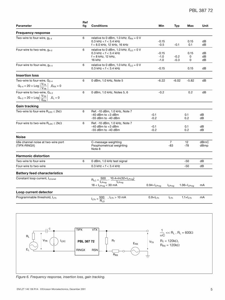
Frequency responseTwo-wire to four-wire, g2-4 6 relative to 0 dBm, 1.0 kHz. ERX = 0 V 0.3 kHz < f < 3.4 kHz -0.15 0.15 dB f = 8.0 kHz, 12 kHz, 16 kHz -0.5 -0.1 0.1 dB
Four-wire to two-wire, g4-2 6 relative to 0 dBm, 1.0 kHz. ELO = 0 V 0.3 kHz < f < 3.4 kHz -0.15 0.15 dB f = 8 kHz, 12 kHz, -1.0 -0.2 0 dB 16 kHz -1.0 -0.3 0 dB
Four-wire to four-wire, g4-4 6 relative to 0 dBm, 1.0 kHz. ELO = 0 V 0.3 kHz < f < 3.4 kHz -0.15 0.15 dB
Insertion lossTwo-wire to four-wire, G2-4 6 0 dBm, 1.0 kHz, Note 5 -6.22 -6.02 -5.82 dB VTX G2-4 = 20 × Log VTR ,ERX = 0
Four-wire to two-wire, G4-2 6 0 dBm, 1.0 kHz, Notes 5, 6 -0.2 0.2 dB VTR G4-2 = 20 × Log ERX ,EL = 0
Gain trackingTwo-wire to four-wire RLDC ≤ 2kΩ 6 Ref. -10 dBm, 1.0 kHz, Note 7 -40 dBm to +3 dBm -0.1 0.1 dB -55 dBm to -40 dBm -0.2 0.2 dB
Four-wire to two-wire RLDC ≤ 2kΩ 6 Ref. -10 dBm, 1.0 kHz, Note 7 -40 dBm to +3 dBm -0.1 0.1 dB -55 dBm to -40 dBm -0.2 0.2 dB
NoiseIdle channel noise at two-wire port C-message weighting 7 12 dBrnC(TIPX-RINGX) Psophometrical weighting -83 -78 dBmp Note 8
Harmonic distortionTwo-wire to four-wire 6 0 dBm, 1.0 kHz test signal -50 dB
Four-wire to two-wire 0.3 kHz < f < 3.4 kHz -50 dB
Battery feed characteristicsConstant loop current, ILConst RLC = 500 - 10.4×ln(32×ILProg) ILProg ILProg 18 < ILProg < 30 mA 0.94×ILProg ILProg 1.06×ILProg mA
Loop current detectorProgrammable threshold, ILTh ILTh =
500 , ILTh > 10 mA 0.9×ILTh ILTh 1.1×ILTh mA RLD
Figure 6. Frequency response, insertion loss, gain tracking.
1 << RL , RL = 600ΩωC
RT = 120kΩ, RRX = 120kΩ
PBL 387 72
TIPX
RINGX RSN
VTX
RT
RRX
ERX
RL
VTR ILDC
C
EL
VTX
RefParameter fig Conditions Min Typ Max Unit
RingingVR input impedance 50 MΩ
Input bias current VR 7 nA
VR input voltage Ref to AGND 0.81 VPeak
Ring injection suppression Active state, RL = 600 Ω 100 dB
Ringing gain VR to two-wire, Note 9 94 ratio
Ringing voltage total distortion RL = 1.4 kΩ - 40 kΩ , 25 Hz, Note 9 0.4 2 %
Voltage offset TIPX and RINGX VBat/2 + 0.65, Note 9 -3 0 3 V
Common mode voltage TIPX and RINGX VBat/2 + 0.65 -0.4 0 0.4 V
Ring-trip detectorRing-trip current threshold, ILRTh Note 10 0.92×ILRTh ILRTh 1.08×ILRTh mA
Loop voltage measurementFrequency f = 106 f Hz VTR + 1
Ground key detector and loop ground fault detectorGround key detector threshold 9 15 19 mA
Digital inputs (C1, C2, C3)
Input low voltage, VIL 0 0.5 V
Input high voltage, VIH 2.5 VCC V
Input low current, IIL VIL = 0.5 V -200 µA
Input high current, IIH VIH = 2.5 V -100 µA
Detector output (DET)
Output low voltage, VOL IOL = 1 mA 0.1 0.6 V
Internal pull-up resistor to VCC 10 kΩ
Power dissipation (VBat -80 V, VTBat = -24 V note 11)
P1 Open circuit state 16 mW
P2 Active state Longitudinal current = 0 mA, IL = 0 mA 65 mW
P3 Active state, RL = 300 Ω (Off-hook) 0.50 W
P4 Active state, RL = 600 Ω (Off-hook) 0.29 W
P5 Ringing state, RL = 7 kΩ (ac load ≈ 1 REN) 0.36 W Sine wave, 20 Hz, max. amplitude
Power supply currents (VBat = -80 V)
VCC current, ICC Open circuit state 1.4 mA
VTBat current, ITBat Open circuit state 0 mA
VTB current, ITB Open circuit state -0.13 mA
VBat current, IBat Open circuit state -0.07 mA
VCC current, ICC Active state, On-hook 2.4 mA
VTBat current, ITBat Active state, On-hook 0 mA
VTB current, ITB Active state, On-hook -0.2 mA
VBat current, IBat Active state, On-hook -0.6 mA
VCC current, ICC Ringing state, On-hook, No ring signal 7.1 mA
VTBat current, ITBat Ringing state, On-hook, No ring signal 0 mA
VTB current, ITB Ringing state, On-hook, No ring signal -1 mA
VBat current, IBat Ringing state, On-hook, No ring signal -2.7 mA
PBL 387 72
6 EN/LZT 146 136 R1A ©Ericsson Microelectronics, December 2001

RefParameter fig Conditions Min Typ Max Unit
Power supply rejection ratios
VCC to 2-wire port Active State f = 1 kHz, Vn = 100 mV 30 45 dB
VCC to 4-wire port Active State f = 1 kHz, Vn = 100 mV 36 51 dB
VTB to 2-wire port Active State f = 1 kHz, Vn = 100 mV 28.5 60 dB
VTB to 4-wire port Active State f = 1 kHz, Vn = 100 mV 34.5 66 dB
VBat to 2-wire port Active State f = 1 kHz, Vn = 100 mV 40 60 dB
VBat to 4-wire port Active State f = 1 kHz, Vn = 100 mV 46 66 dB
Temperature guardJunction threshold temperature, TJG 155 °C
Thermal ResistanceJunction to pin, ΘJP 22 °C/W
Junction to ambient, ΘJA 41.6 °C/W
Notes, Electrical characteristics1. The overload level is automatically expanded to needed
signal level, maximum 1.7 VPeak when the signal level is > 1.0 VPeak , and is specified at the two-wire port with the signal source at the four-wire receive port. For more information see section Adaptive overhead voltage.
2. The two-wire impedance is programmable by selection of external component values according to:ZTRX = ZT/(G2-4S × αRSN)
where:ZTRX = impedance between the TIPX and RINGX terminals
ZT = programming network between the VTX and RSN terminals
G2-4S = transmit gain, nominally = 0.5
αRSN = receive current gain, nominally 400 (current defined as positive flowing into the receive summing node, RSN, and when flowing from ring to tip). See section Transmission.
3. Higher return loss values can be achieved by adding a reactive component to ZT, the two-wire terminating impedance programming resistances, e.g. by dividing ZT, into two equal halves and connecting capacitors from the common points to ground.
4. The overload level is automatically expanded as needed up to 1.25 VPeak (using the AOV function) when the signal level >0.5 VPeak and is specified at the four-wire transmit port, (VTX) with the signal source at the two-wire port. Note that the gain from the two-wire port to the four-wire transmit port is G2-4S = 0.5.
5. Secondary protection resistors RF1 and RF2 impact the insertion loss (refer to section Transmission). The specified insertion loss is for RF1 = RF2 = 40Ω.
6. The specified insertion loss tolerance does not include errors caused by external components.
7. The level is specified at the four-wire receive port (ERX, figure 6) and referenced to a 600 Ω impedance level.
8. The two-wire idle noise is specified with the four-wire receive port grounded (ERX = 0, figure 6). The four-wire idle noise at VTX is the two-wire value reduced by 6 dB and is specified with the two-wire port terminated in 600 Ω (RL). The VTX noise specification is referenced to a 600 Ω impedance level.
9. PBL 387 72/1 contains an Automatic Gain Control Ringing (AGC-R) unit. This unit controls the Gain in the ringing loop to keep an undistorted ringing signal due to variation in VBAT, VR input signal amplitude and Voltage offset. For more information see section Ringing further on.
10. See section Calculation of the ring-trip threshold for information about this.
11. The VTBAT voltage is optimized for RL=600 Ω , IL = 26.8 mA, no metering signal, RF = 40 and the current controlled battery switch. See section Optimizing VTB for further information.
PBL 387 72
7 EN/LZT 146 136 R1A ©Ericsson Microelectronics, December 2001

Pin Description Pin Symbol Description1 BW Batwing (refer to Note, Pin Description)
2 BW Batwing (refer to Note, Pin Description)
3 BW Batwing (refer to Note, Pin Description)
4 HP High Pass AC/DC separation capacitor CHP connects between this pin and TIPX.
5 BGND Battery Ground. Shall be tied together with AGND.
6 RINGX The RINGX pin connects to the ring lead of the two-wire interface via over voltage protection components (and optional test access switch).
7 TIPX The TIPX pin connects to the tip lead of the two-wire interface via over voltage protection components (and optional test access switch).
8 VTBAT Talk Battery. The dc loop current is supplied to TIPX and RINGX from this battery voltage. Negative with respect to BGND.
9 VBAT On-hook Ringing Battery supply voltage. Negative with respect to BGND.
10 VTB Internal SLIC bias voltage. Connected to the talk battery supply. Refer to the application diagram in figure 8. May be connected to any voltage between -32 and –10 V.
11 LP Low Pass saturation guard filter capacitor CLP connects between this pin and VTBAT to filter out noise and improve PSRR.
12 SPR Silent Polarity Reversal. The polarity reversal time can be set with a capacitor connected between this pin and AGND.
13 BW Batwing (refer to Note, Pin Description)
14 BW Batwing (refer to Note, Pin Description)
15 CRING The capacitor CRING connects between this pin and AGND. Required for the ring signal generation.
16 REF A 15 kΩ resistor connected between this pin and AGND sets an internal SLIC reference current. The value must not be changed.
17 PLC Programmable Line Current. The constant current DC feed is programmed by a resistor connected from this pin to AGND.
1
2
3
4
5
6
7
8
9
10
11
28
27
26
25
24
23
22
21
20
19
18
BW
BW
BW
HP
BGND
RINGX
TIPX
VTB
C1
VTX
RSN
AGND
VR
C2
C3
PLD
LP
VBAT
DET
VTBAT
VCC
12 17SPR PLC
28-pin SOIC
16 REF
15 CRING
13BW
14BW
PRT
PBL 387 72
8 EN/LZT 146 136 R1A ©Ericsson Microelectronics, December 2001
Figure 7. Pin configuration 28L-SOIC, top view.
18 PRT Programmable Ring-trip Resistor RRT connected between this pin and AGND. Sets the ring-trip threshold. The capacitor CRT together with resistor RRT filters the ring-trip detector.
19 PLD Programmable Loop Detector threshold. The loop detection threshold is programmed by a resistor, RLD, connected between this pin and AGND.
20 VCC +5 V power supply.
21 C3 C1, C2, C3 are digital inputs, which control the SLIC
22 C2 operating states. Refer to table 1 for details.
23 C1
24 DET Detector output. Active low when indicating loop or ring-trip detection, active high when indicating ground key detection.
25 VR Low voltage ringsignal input.
26 AGND Analog Ground, shall be tied together with BGND.
27 RSN Receive Summing Node. 400 times the current flowing out of this pin equals the metallic (transversal) current flowing from RINGX to TIPX. Programming networks for two-wire impedance and receive gain connect to the receive summing node.
28 VTX Transmit vf output. The ac voltage difference between TIPX and RINGX, the ac metallic voltage, is reproduced at VTX with a gain of 0.5. The two-wire impedance programming network connects between VTX and RSN.
Note: A batwing is a package pin, which provides a low thermal resistance path to the silicon chip via the lead frame. By soldering the batwing pins to PCB copper foil the device can be efficiently cooled. Note that batwing pins are at the same voltage as the VBAT pin (substrate voltage).
PBL 387 72
9 EN/LZT 146 136 R1A ©Ericsson Microelectronics, December 2001
SLIC Operating States State C3 C2 C1 SLIC Operating State Active detector (DET response)
0 0 0 0 TIPX & RINGX open circuit No active detector (DET is set high)
1 0 0 1 Ringing Ring-trip detector (DET active low)
2 0 1 0 Active Loop current detector (DET active low)
3 0 1 1 Active Loop voltage measurement (DET pulse train)
4 1 0 0 Not applicable –
5 1 0 1 Active Ground key detector and loop ground fault detector (DET active high)
6 1 1 0 Active, reverse polarity Loop current detector (DET active low)
7 1 1 1 Active, reverse polarity Ground key detector and loop ground fault detector (DET active high)
Table 1. SLIC operating states.

Functional Description and Applications Information
DBB is normally reverse biased, but conducts supply VTB to the VBAT terminal in case the voltage VB would fail.
RT sets the two-wire impedance (note that RT may be replaced with a complex impedance, ZT, to implement complex terminating impedance).
RRX sets the receive gain.
RLD sets the loop current detector threshold.
RLC sets the constant dc loop current.
RREF sets a SLIC reference current (must be 15.0 kΩ, 1%, as specified).
RRT sets the ring trip loop current detector threshold.
CRING is used for the high voltage ringing signal AGC (automatic gain control) function.
VTB is the talk battery supply, i.e. the negative supply voltage that sources the loop current.
VB is the ringing battery, i.e. the negative supply voltage that is used to power the SLIC, while ringing the line. This battery is also used to provide on-hook voltage.
Design supporting tools
The following supporting tools are available for the PBL 387 72/1:- Test board, TB 215- Pspice model PBL 387 72/1
Introduction
The Figure 8 diagram shows the PBL 387 72/1 in a typical application with a non-programmable, Combo I, codec. The PBL 387 72/1 can equally well be used with programmable codecs. This SLIC is suitable in short loop power sensitive application like, Cable modem, Voice over DSL, ISDN terminal adapter (NT1+), Voice over IP, Integrated Access Device (IAD), Residential Gateway or other short loop application. The component values chosen for the application diagram example yield a two-wire impedance of 600 Ω, resistive. The balance resistor is calculated for line impedance, ZL (compromise impedance), of 600 Ω, resistive. The two-wire to four-wire gain is set by RTX and RFB to produce the digital mW level at the PCM transmit bus.
RF1, RF2 and the clamp “OVP” make up the overvoltage protection network.
The ratio between RFB and RTX sets the transmit gain.
CTC and CRC clamp fast transients that may bypass the OVP clamp and also filter high frequency interference (RFI filter).
CHP and CLP are coupling capacitors within two SLIC feedback loops that control SLIC battery feed and SLIC voice frequency transmission.
CTB, CB, CVCC are power supply bypass capacitors.
DTB is a diode that is part of the battery switching function.
DB prevents reverse currents from the VB supply rail during application of negative over voltages.
PBL 387 72
10 EN/LZT 146 136 R1A ©Ericsson Microelectronics, December 2001

Figure 8. Single channel subscriber line interface with PBL 387 72/1 and Combo I type codec.
PBL 387 72/1 components
RESISTORS :
(values according to IEC-63 E96 series)RLD = 49.9 kΩ 1% 1/10 WRLC = 18.7 kΩ 1% 1/10 WRRT = 61.9 kΩ 1% 1/10 W @ VBAT = 80 VRREF = 15 kΩ 1% 1/10 W
RT = 105 kΩ 1% 1/10 W (for 600 Ω two- wire impedance with the RF1 and RF2 included.)
RRX = 105 kΩ 1% 1/10 W (The gain is set to 1)RVR = 200 kΩ 1% 1/10 WRTX = 32.4 kΩ 1% 1/10 WRB = 57.6 kΩ 1% 1/10 WRFB = depending on codecRF1 = RF2 = Line protection resistor, 40Ω 1% match, e.g. by Bourns TBD
CAPACITORS:
(values according to IEC-63 E6 series)CTB = 150 nF 100 V 20%CB = 100 nF 100 V 20%CVCC = 100 nF 10 V 20%CHP = 33 nF 100 V 20%CLP = 470 nF 100 V 20%CGG = 220 nF 100 V 20%CRING = 470 nF 10 V 20 %CRT = 10 nF 10 V 20 %CVR = 470 nF 10 V 20 %
OPTIONAL CAPACITORS:
CTC = 1.0 nF 100 V 20%CRC = 1.0 nF 100 V 20%CSPR = optional 10 V 20%
DIODES:
DB = DTB = DBB =TBD
OVP:
Secondary protection clamp (e.g. Bourns/Power Innovations TISP PBL3 or TISP 6NTP2A ,which serves two lines).The ground terminals of the secondary protection should be connected to the common ground on the Printed Board Assembly with a track as short and wide as possible, preferably to a ground plane.
CTB
DB
CLP
DTB
VTB
VB
CRC
OVPVB
RF1
RF2
CGG
CTC
PLD
PRT
PLC
REF
PLDVTB
LP
SPR
BW
RSN
AGND
VR
DET
HP
BW
BW
BGND
BW VTX
PBL38772
C2
RINGX C1
C3
VCC
TIPX
VTBAT
VBAT
RTX
RRX
TIP
RING
CRING
CB BW CRING
CHP
VCC
CVR
VR
CSPR
SYSTEM CONTROLINTERFACE
0
-
+
0
CODEC/Filter
-
+
TXPCMbus
RXPCMbus
DX
DR
RREF
RFB
CVCC
RT RB
RVR
DBB
RLCCRTRRT RLD
PBL 387 72
11 EN/LZT 146 136 R1A ©Ericsson Microelectronics, December 2001

Figure 9. Simplified AC model of PBL 387 72/1.
TransmissionGeneral
A simplified ac model of the transmission circuit is shown in figure 9. Circuit analysis yields:
VTR = VTX + IL × 2RF (1)
G2-4S
IL = VTX + VRX (2)αRSN ZT ZRX
VTR = EL - IL × ZL (3)
where:VTX is the ground referenced ac voltage at the VTX terminal.
VTR is the ac metallic voltage between tip and ring.
EL is the line open circuit ac metallic voltage.
IL is the ac metallic current.
RF is a line over voltage protection resistor.
G2-4S is the SLIC two-wire to four-wire gain (transmit direction) with a nominal value of 0.5.
ZL is the total line impedance
ZRX controls four- to two-wire gain.
ZT determines the SLIC TIPX to RINGX ac impedance for signals at voice frequencies.
VRX is the analog ground referenced receive signal.
αRSN is the receive summing node current to metallic loop current gain. αRSN = 400
RHP internal resistor, approx. 400 kΩ
Two-Wire Impedance
To calculate ZTR, the impedance presented to the two-wire line by the SLIC including the line protection resistors RF , let VRX =0.
From (1) and (2):
ZTR = ZT
+ 2RF (4) αRSN × G2-4S
Thus with ZTR, G2-4S, αRSN and RF known:
ZT = αRSN × G2-4S × (ZTR - 2RF) (5)
Two-Wire to Four-Wire Gain
From (1) and (2) with VRX =0:
G2-4 = VTX = ZT/αRSN (6) VTR ZT +2RF αRSN × G2-4S
Four-Wire to Two-Wire Gain
From (1), (2) and (3) with EL = 0:
G4-2 = VTR = - ZT × 1 × ZL (7) VRX ZRX G2-4S ZT + ZL + 2RF αRSN × G2-4S
For applications where ZT +2RF = ZL αRSN × G2-4S
the expression for G4-2 simplifies to:
G4-2 = - ZT × 1 (8) ZRX 2 × G2-4S
PBL 387 72
+
-+
-
VTX
RSN
IL/α
TIPX
RINGX
+
-
EL
+
-
TIP
RING
RF
RF
ZTR
ZT
VTX
VRX
ZRX
IL
IL
RHP
+
-
ZL
VTR G
RSN
2-4S
HP
PBL 387 72
12 EN/LZT 146 136 R1A ©Ericsson Microelectronics, December 2001
Four-Wire to Four-Wire Gain
From (1), (2) and (3) with EL = 0:
G4-4 = VTX = - ZT × ZL + 2RF (9) VRX ZRX ZT + ZL + 2RF αRSN × G2-4S
Hybrid Function
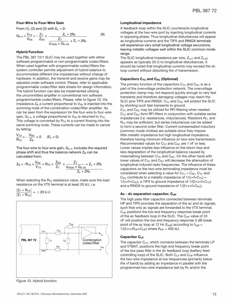
The PBL 387 72/1 SLIC may be used together with either software programmable or non-programmable codec/filters. When used together with programmable codec/filters the system controller permits adjustment of hybrid balance to accommodate different line impedances without change of hardware. In addition, the transmit and receive gains may be adjusted under software control. Please, refer to applicable programmable codec/filter data sheets for design information.The hybrid function can also be implemented utilizing the uncommitted amplifier in conventional non software programmanble codec/filters. Please, refer to figure 10. Via impedance ZB a current proportional to VRX is injected into the summing node of the combination codec/filter amplifier. As can be seen from the expression for the four-wire to four-wire gain, G4-4, a voltage proportional to VRX is returned to VTX. This voltage is converted by RTX to a current flowing into the same summing node. These currents can be made to cancel by letting:
VTX = - VRX = 0 (EL = 0)
RTX ZB
The four-wire to four-wire gain, G4-4, includes the required phase shift and thus the balance network ZB can be calculated from:
ZB = -RTX × VRX = RTX × ZRX × ZT + ZL + 2RF VTX ZT αRSN × G2-4S ZL + 2RF
When selecting the RTX resistance value, make sure the load resistance on the VTX terminal is at least 20 kΩ, i.e.
ZT × RTX = ≥ 20 k Ω ZT + RTX
Longitudinal impedance
A feedback loop within the SLIC counteracts longitudinal voltages at the two-wire port by injecting longitudinal currents in opposing phase. Thus longitudinal disturbances will appear as longitudinal currents and the TIPX and RINGX terminals will experience very small longitudinal voltage excursions, leaving metallic voltages well within the SLIC common mode range.The SLIC longitudinal impedance per wire, ZLoT and ZLoR, appears as typically 20 Ω to longitudinal disturbances. It should be noted that longitudinal currents may exceed the dc loop current without disturbing the vf transmission.
Capacitors CTC and CRC (Optional)
The primary function of the capacitors CTC and CRC is as a part of the overvoltage protection network. The overvoltage protection clamp may not respond quickly enough to very fast transients and therefore damaging voltages may reach the SLIC pins TIPX and RINGX. CTC and CRC will protect the SLIC by shorting such fast transients to ground.CTC and CRC may be utilized for RFI filtering when needed. CTC and CRC form RFI filters in conjunction with suitable series impedances (i.e. resistances, inductances). Resistors RF1 and RF2 may be sufficient, but series inductances can be added to form a second order filter. Current-compensated inductors (common mode chokes) are suitable since they impose little metallic impedance but high longitudinal impedance, therefore having minimum influence on two-wire transmission. Recommended values for CTC and CRC are 1 nF or less. Lower values implies less influence on the return loss and less degradation of the longitudinal balance caused by missmathing between CTC and CRC. On the other hand with lower values of CTC and CRC will decrease the attenuation of longitudinal induced radio frequencies. The influence of these capacitors on the two-wire terminating impedance must be considered when selecting a value for CTC = CRC. CTC and CRC contribute to a metallic impedance of 1/(π×f×CTC) = 1/(π×f×CRC), a TIPX to ground impedance of 1/(2×π×f×CTC) and a RINGX to ground impedance of 1/(2×π×f×CRC).
Ac - dc separation capacitor, CHP
The high pass filter capacitor connected between terminals HP and TIPX provides the separation of the ac and dc signals, such that only ac signals are forwarded to the VTX terminal. CHP positions the low end frequency response break point of the ac feedback loop in the SLIC. The CHP value of 33 nF will position the low end frequency response 3 dB break point of the ac loop at 12 Hz (f3dB) according to f3dB = 1/(2×π×RHP×CHP) where RHP = 400 kΩ.
Capacitor CLP
The capacitor CLP, which connects between the terminals LP and VTBAT, positions the high end frequency break point of the low pass filter in the dc feedback loop (battery feed controlling loop) of the SLIC. Both CLP and CHP influence the two-wire impedance at low frequencies (primarily below the vf band) by adding an impedance in parallel with the programmed two-wire impedance (set by RT and/or the
Figure 10. Hybrid function.
VT
Combinationcodec/filter
RTX
ZB
ZRX
ZT
VTX
RSN
VRX
PBL 387 72
RFB
PBL 387 72
13 EN/LZT 146 136 R1A ©Ericsson Microelectronics, December 2001
Z-filter in the codec). The SLIC SPICE model includes the effects of CLP and CHP on the vf transmission. The CLP value of 470 nF will position the high end frequencyresponse 3 dB break point of the ac loop at 0.3 Hz (f3dB).
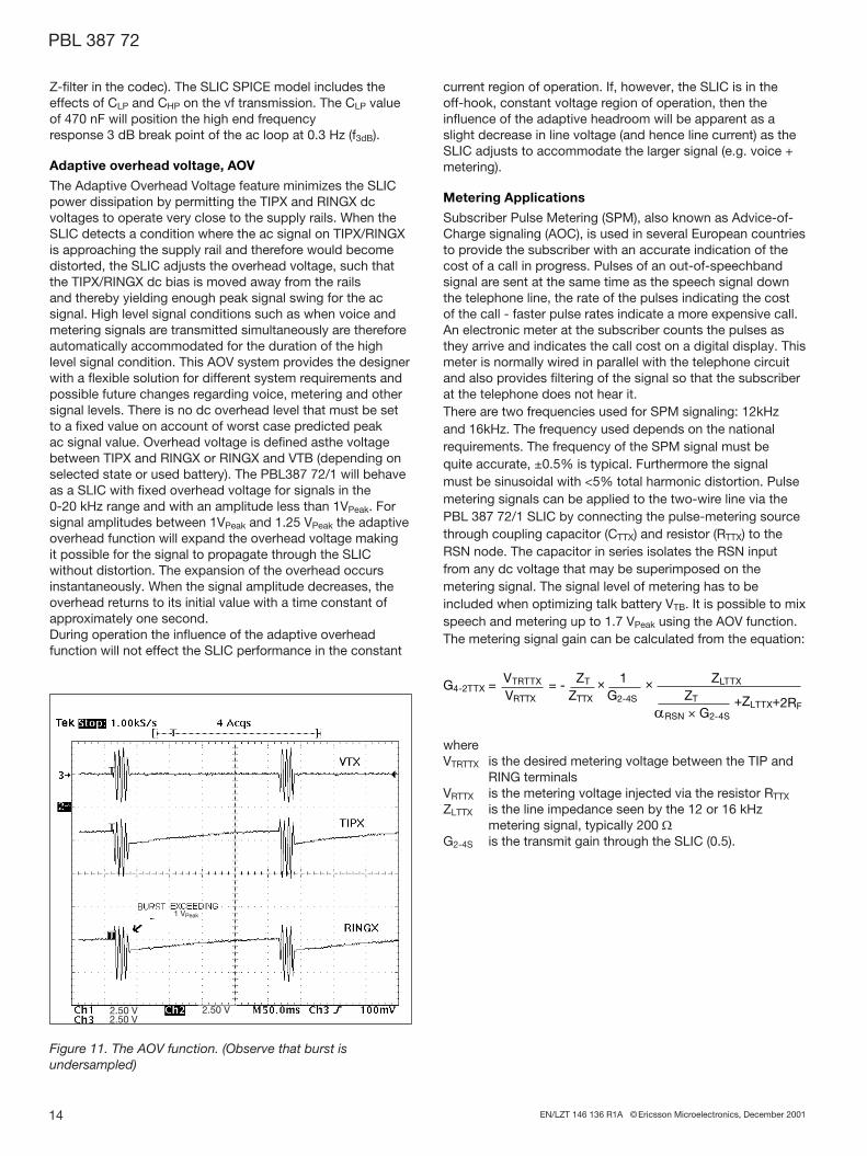
Adaptive overhead voltage, AOV
The Adaptive Overhead Voltage feature minimizes the SLIC power dissipation by permitting the TIPX and RINGX dc voltages to operate very close to the supply rails. When the SLIC detects a condition where the ac signal on TIPX/RINGX is approaching the supply rail and therefore would become distorted, the SLIC adjusts the overhead voltage, such that the TIPX/RINGX dc bias is moved away from the rails and thereby yielding enough peak signal swing for the ac signal. High level signal conditions such as when voice and metering signals are transmitted simultaneously are therefore automatically accommodated for the duration of the high level signal condition. This AOV system provides the designer with a flexible solution for different system requirements and possible future changes regarding voice, metering and other signal levels. There is no dc overhead level that must be set to a fixed value on account of worst case predicted peak ac signal value. Overhead voltage is defined asthe voltage between TIPX and RINGX or RINGX and VTB (depending on selected state or used battery). The PBL387 72/1 will behave as a SLIC with fixed overhead voltage for signals in the 0-20 kHz range and with an amplitude less than 1VPeak. For signal amplitudes between 1VPeak and 1.25 VPeak the adaptive overhead function will expand the overhead voltage making it possible for the signal to propagate through the SLIC without distortion. The expansion of the overhead occurs instantaneously. When the signal amplitude decreases, the overhead returns to its initial value with a time constant of approximately one second.During operation the influence of the adaptive overhead function will not effect the SLIC performance in the constant
1 VPeak
2.50 V2.50 V2.50 V
current region of operation. If, however, the SLIC is in the off-hook, constant voltage region of operation, then the influence of the adaptive headroom will be apparent as a slight decrease in line voltage (and hence line current) as the SLIC adjusts to accommodate the larger signal (e.g. voice + metering).
Metering Applications
Subscriber Pulse Metering (SPM), also known as Advice-of-Charge signaling (AOC), is used in several European countries to provide the subscriber with an accurate indication of the cost of a call in progress. Pulses of an out-of-speechband signal are sent at the same time as the speech signal down the telephone line, the rate of the pulses indicating the cost of the call - faster pulse rates indicate a more expensive call. An electronic meter at the subscriber counts the pulses as they arrive and indicates the call cost on a digital display. This meter is normally wired in parallel with the telephone circuit and also provides filtering of the signal so that the subscriber at the telephone does not hear it. There are two frequencies used for SPM signaling: 12kHz and 16kHz. The frequency used depends on the national requirements. The frequency of the SPM signal must be quite accurate, ±0.5% is typical. Furthermore the signal must be sinusoidal with <5% total harmonic distortion. Pulse metering signals can be applied to the two-wire line via the PBL 387 72/1 SLIC by connecting the pulse-metering source through coupling capacitor (CTTX) and resistor (RTTX) to the RSN node. The capacitor in series isolates the RSN input from any dc voltage that may be superimposed on the metering signal. The signal level of metering has to be included when optimizing talk battery VTB. It is possible to mix speech and metering up to 1.7 VPeak using the AOV function.The metering signal gain can be calculated from the equation:
G4-2TTX = VTRTTX = - ZT × 1 × ZLTTX
VRTTX ZTTX G2-4S ZT +ZLTTX+2RF αRSN × G2-4S
whereVTRTTX is the desired metering voltage between the TIP and
RING terminalsVRTTX is the metering voltage injected via the resistor RTTX
ZLTTX is the line impedance seen by the 12 or 16 kHz metering signal, typically 200 Ω
G2-4S is the transmit gain through the SLIC (0.5).
Figure 11. The AOV function. (Observe that burst is undersampled)
PBL 387 72
14 EN/LZT 146 136 R1A ©Ericsson Microelectronics, December 2001

Battery Feed and Automatic Battery SwitchingTo reduce short loop power dissipation a second lower battery voltage, Off-hook or Talk battery, must be connected to the device via an external diode at terminal VTBAT. The SLIC automatically switches between the two battery supply voltages without need for external control. The silent battery switching to VBAT occurs when the line current is below 5.5 mA. This means that the current in On-hook, VBAT, battery is limited to 6 mA in the Active state. The On-hook voltage is derived from VBAT with the range of -43 V to -56 V at the TIPX and RINGX wires @ VBat ≥ -48 V.
Constant current feed region (figure 12, curve segment A-B-C)
For TIPX to RINGX voltages VTR < |VTB| – 5.7 VwhereVTR = the tip to ring dc voltageVTB = the talk battery voltage5.7 V = the voltage drop from VTB to the line voltage
at point C in the graph of figure 12, calculated according to:
0.7 V + 3.7 V + (27 mA × 2 × 25 Ω) ≈ 5.7 V
The PBL 387 72/1 emulates constant current loop feed. The constant current value is adjustable between 18 mA and 30 mA by setting a value for resistor RLC:
RLC = 500 - 10.4 × ln(32 × ILProg) ILProg ILProg
which may be approximated by
RLC ≈ 500 ILProg
whereILProg desired constant current in ARLC programming resistance in Ωln( ) natural logarithm
Resistive feed region (figure 12, curve segment C-D-E)
For VTR > VTB -5.7 V the PBL 387 72/1 emulates resistive loop feed with feed resistance equal to 2x25 Ω. The slope of the resistive feed region is made steep to extend the constant current region as close to the talk battery voltage (VTBat) as possible.
On-hook region (figure 12, curve segment E-G-H-J)
For loop currents IL < 5.5 mA the PBL 387 72/1 automatically switches to feed loop current from the ring battery, VBat. The switch from talk battery, VTBat, to ring battery, VBat, occurs without hysteresis at point E in figure 12. For loop currents IL within the on-hook range 0 mA < IL < 5.0mA (curve segment G-H-J) the line voltage remains nearly constant. This feature maintains a high on-hook voltage in the presence of dc line leakage currents or when asubscriber device consumes some current from the battery
feed, e.g. to power displays. The On-hook voltage tracks the VBAT voltage up to 54.5 V, VTROpen = VBat – 4.5 V. For VBAT higher than 54.5 V the On-hook voltage is limited to 50 V typical.In the presence of leakage currents ILLk < 5 mA during on-hook: (Figure 12, curve segment G-H-J)VTROn-hook = VTROpen - ILLk × RFeed where RFeed = 2×25 Ω
Optimizing VTB
To optimize VTB with actual load on the line:VTB = (RLMax + RFEED + 2RF) × ILprog + VF + 3.7where:RLmax is the maximum loop length including On-hook phone loadRFeed 2×25 ΩRF is the resistance of one fuse resistor.ILProg is the programmed line currentVF is the forward voltage of DTB Normal value is 0.7 VExample: RLmax = 600 Ω, RF = 40 Ω, ILProg = 26.8 mA This will give a VTB of 24 V.
Silent Polarity ReversalPolarity reversal time.
The reversal time is set by a capacitor, CSPR, connected between the pin SPR and AGND. The silent polarity reversal time is the same in both directions. To calculate the silent polarity reversal time use the following formula:tr =CSPR × 9500The reversal time is measured between the 10% and 90% values of the line voltage. The reversal time is independent of line load and line current.
Polarity reversal set-up time.
The set-up time is defined as the time from setting the C1, C2 and C3 inputs to the reversal state until the reversal actually commences on TIPX and RINGX.The polarity reversal set-up time is different in the two directions, active to reversal state and reversal to active state.The set-up time is calculated from the following expressions:Active normal state to active reversal state: tAct→Rev = CSPR × 17500Active reversal state to active normal state: tRev→Act = CSPR × 15500
PBL 387 72
15 EN/LZT 146 136 R1A ©Ericsson Microelectronics, December 2001

A: IL (@VTR=0) = ILconst = ILProg RLC = 500 - 10.4 × ln(32 × ILProg) ILProg ILProg
B,C: IL = ILconst , VTR(@C) = VApp - RFEED × ILProg
D: RFEED = 2×25 Ω
E: IL ≈ 5.5 mA , VTR = VApp - RFEED × 5.5 mA
F: VApp (@IL = 0) = VTB - VF* - 3.7 V * VF is the forward voltage drop across diode DTB
G: IL ≈ 5 mA
H: RFEED = 2 × 25 Ω
J: The On-hook voltage tracks the VBAT voltage up to |54.5| V, VTROpen = |VBat| – 4.5 V. For VBAT > |54.5| V, VTROpen = 50 V.
D
B
E
G
H
CA
V TR [V]
IL [
mA
]
F J
Figure 12. Battery feed characteristics.
Ringing VoltageWhen designing PBL 387 72/1 the object was to design a robust ringing SLIC that supports balanced ringing and that handles the high power dissipation and the different fault conditions that may occur when ringing. For power handling see section Power control.Figure 13 shows a high level schematic of the ring loop.The ring loop in the PBL 387 72/1 is designed as a voltage amplifier. An internal feedback loop from the two-wire to the input sets a predetermined voltage gain. The voltage gain is adjusted to 94 by the AGC-R when ringing. The power amplifiers are of the current feed type that makes it possible to provide a reliable control of the ringing current. This arrangement makes it possible to add a control device, including an Automatic Gain Control unit, that provides protecting functions, such as:
Automatic Gain Control-Ringing, AGC-R: If the amplifiers that supply Tip and Ring are forced to saturation due to i.e. variations of the VBat voltage or the VR input signal level, the AGC-R will decrease the output signal. The shape of the output signal is kept undistorted. This function guarantees a low output impedance, approximately 2×20 Ω, and also allows variations in the input signal and the VBat voltage.
Current limit: At off-hook or in fault conditions, i.e. Tip and Ring are shorted, the control device will limit the ringing current to approximately 10 mA above the programmed ring-trip threshold.
PBL 387 72
16 EN/LZT 146 136 R1A ©Ericsson Microelectronics, December 2001

Figure 13. Ring loop schematic.
Foreign voltage protection: The control device will detect if Tip and/or Ring are shorted to e.g. ground. The output voltage will be shut off to keep the power down. The detector output will be high.
Temperature management: If the chip temperature exceeds 155 °C the control device will reduce the output voltage until the chip temperature equals 155 °C, and increase it again when the temperature drops. The detector output, DET, is forced to a logic low level when the temperature guard is active.
The VR pin is a high impedance input. The voltage VR has a reference to AGND. This input has to have a resistor, RVR = 200 kΩ, connected to ground, and a capacitor, CVR = 470 nF, in series to decouple the DC component. The input handles any waveform, e.g. sinusoidal, trapezoid or square-wave shaped signals, since the SLIC acts like a linear amplifier. When using a square-wave input signal it has to be filtered and therefore add a capasitor of 10 nF parallel with the RVR resistor. A DC-offset can be obtained by adding a DC part to the input signal. The capacitor CRING forms a low pass filter that is an essential part of the control device. The control is used to control e.g. the applied output voltage, the ringing current or the chip temperature. The resistor RRT is a programming resistor that sets the ring-trip detector threshold. The current through the resistor is a rectified version of the line current divided by a factor The capacitor CRT filters the ring-trip detection device. PRT-pin is connected to the negative input of an OP-amplifier. The positive input is connected to a reference voltage. The output of the OP-amplifier is connected to the detector output DET. When the voltage over the resistor RRT exceeds the reference voltage the detector output changes state.The ring injection will be describes in more detail with figure 14 and 16. Figure 14 shows a ring sequence with an off-hook at time t1. The first diagram shows the voltage applied to the input, VR, together with the voltages at TIPX and RINGX pins. The voltage of the TIP wire follows the voltage of the VR pin. The second diagram shows the rectified current, IL/α through the resistor RRT. The dotted line represent the programmed ring-trip threshold, ILTH/α The third diagram shows the voltage on the detector output. Before time t1, the phone supposed to be on-hook. The ring voltage is applied symmetrically around a fixed voltage, VBat/2, to the load. As long as the telephone is on-hook the rectified current IL/α will not exceed
Figure 14. Off-hook during ringing. Figure 15. Off-hook during Ringing with an applied DC offset.
RL
CRING
VR
PA
Tip
IL
IL
VTR
DET
+
-
RINGIL
Temp.
RRT
PARING
TIP
PRTCRING
ILαControl
device
CRT
PBL 38772/1
20 Ω
20 Ω
+
-
GND
VR
GND
VBAT
TIP
RING
VBAT/2
U [V]
t [s]
DET [V]
[A]
t [s]
t [s]
ILTH/α
VR
IL/α
t1
t1
t1
GND
VBAT
TIP
RING
VBAT/2
U [V]
t [s]
DET [V]
IL/α [A]
t [s]
t [s]
ILTH/α
VR
t1
t1
t1
PBL 387 72
17 EN/LZT 146 136 R1A ©Ericsson Microelectronics, December 2001

ILTH/α. The DET output will be high. The control device will make sure that the voltage over the load is as high as possible without saturating the power amplifiers. When the telephone goes off-hook, at time t1, the impedance of the load will decrease. The line current will increase and the control device will reduce the line current to a maximum of approximately 10 mA above the programmed ring-trip threshold, ILTH. When the rectified current, IL/α exceeds or equals to ILTH/α the detector output, DET, will change to a logic low level, i.e. an off-hook. The voltage of the load will be reduced as a result of the control device limiting the line current. The figure 15 illustrates ringing with a DC offset. This method is useful when trying to extend the ring-trip capability. When programming the ring-trip threshold there must be some margin so that no false ring-trip occurs when ringing at high REN. In on-hook the DC voltage will not have any affect on the load since there is no DC path, but when the telephone goes off-hook there will be a DC path and the extra voltage will give a high ring current. This arrangement makes it possible to set a higher ringtrip threshold value and thereby gives a larger margin between the ring current in on-hook, with low RENs, and the ring current in off-hook. To keep the same amplitude on the AC signal, as when ringing without DC offset, the battery has to be increased by the same value as the programmed dc offset. The signal to VR-pin is supplies with a positive DC offset to AGN. The signal on the Tip-wire will be applied with a positeve DC offset to the fixed voltage VBat/2. The signal on the Ring-wire will be applied with a negative dc offset.
Calculation of the input signal
The VR input have to be connected to a signal generator or via impedance in all states. The following equations are valid for ring load between 0.25 and 5 REN. The optimal signal at VR pin is calculated as follows:
VRPK = |VBat| - 3.5 (17) 94.4Where:VRPK is the peak value at the VR pin.VBat is the voltage of the VBAT pin.Example: VBat = 80V
This will give: VRPK = 0.81 VPK
With DC-offset:
VRDC = VRDCT-R (18) 109.6
VRPK+DC = |VBat| - 3.5 - VRDC (19) 94.4
Where:VRDC is the positive DC offset in respect to GND at VR pin.VRDCT-R is the DC voltage difference between the TIP and
RING wires.VRPK+DC is the peak value of the AC-signal to be
superimposed to the DC-voltage VRDC.Example: VBat = -80 V, VRDCT-R = 10 VThis will give: VRDC = 0.091 V and VRPK+DC = 0.718 VPK
Calculation of the ring-trip threshold
The ring-trip threshold is calculated according to the equation:
RRT = 3750 × ZBellmin + 40 + 2×RF + RLmin (20) |VBat| × αMax - 3.5
With DC-offset:
RRT = 3750 × ZBellmin + 40 + 2×RF + RLmin (21) |VBat| × αMax - 3.5 - VRDCT-R
Where: 40 is the resistance of the SLICs internal resistors
connected in series with output amplifiers see figure 13. RRT is the resistor value of the resistor connected
between the PRT-pin and GND. VBat is the voltage of the VBAT pin.αMax is the variation of the battery. 2% will give an α=1.02.ZBellmin is the minimum resistance of the bell in on-hook.
Typical 1400 Ω for 5 REN.RF is the resistance of one fuse resistor. RLmin is the resistance of the minimum loop length.VRDCT-R is the DC voltage difference between the Tip and
Ring wire.Example: VBat = -80 V, ZBellMin = 1300 Ω, αMax = 0%, RF = 40 Ω , VRDCT-R = 0, RLmin = 0 Ω, This will give: RRT = 69.6 kΩ and a Ring-trip current threshold,
ILRth = 57.5 mA
ILRth = 4000 (22)
RRT
Power Dissipation ConsiderationsThermal design considerations
The thermal resistance, ΘJa, of the PBL387 72/1 in a 28-pin SOIC package is 41.6 °C/W. The junction to ambient thermal resistance value, ΘJa, is extracted using the SEMI standard G38-0996 and is representative of the natural airflow as seen in an application with a multilayer board. In this device the thermal resistance is lowered by using batwing pins, i.e. pins that are thermally and electrically shorted to the die. This also means that the potential of the batwing pins are the same as the substrate potential, i.e. the VBat potential. To reduce the thermal resistance in critical applications these batwing pins must be used. Typical demanding applications involves high ring voltages, high DC-offset, high REN numbers, high line currents together with high talk battery and used in high ambient temperatures. In these type of applications the batwing pins shall be soldered to a large metal layer using thermal conducting vias, i.e. small vias that will be filled with solder during the soldering process. The metal layer shall be of the order of 1sq inch and most effective is to use an outer layer, which can be cooled by convection. The PBL387 72/1 has a thermal shutdown protection at a typical temperature, TJG of 155 °C, see Analog temperature guard.
PBL 387 72
18 EN/LZT 146 136 R1A ©Ericsson Microelectronics, December 2001
There are three situations where high power dissipation occurs.1. Ringing power dissipation on-hook2. Ringing power dissipation off-hook3. Off-hook power dissipation
1. Ringing power dissipation on-hook
The power dissipation can be calculated by the following formula:
PRNG = PR × tR + PA × tA
tR + tA tR +tA
where:PRNG Average power during ringing.PR Power in Ring state.PA Power in Active state P2 in the specification typical
around 65 mWtR Time in Ring statetA Time in Active state
Ringing is normally applied with a defined ring cadence with burst and silent intervals where the SLIC is switched between the ring and active state. Typically the time tA is four times the time tR. In some applications the time for the ringing and silent periods are equal, and the SLIC will dissipate more power.
The power dissipation in the SLIC for the burst can be calculated using:PR = PS - POut =For a sinusodial shaped ring signal:
= 2 × VBAT × VRing - VRing2 × cosΘL + PRingBias π ZLoop 2ZLoop
where:Ps Supply powerPOut Output powerVBAT potential at pinVRing peak to peak voltage between tip and ring during
ringingPRingBias power dissipation in ring state without load, typical
value 0.3 WZLoop total line impedance, including fuse and the
telephone impedance (in this case the on-hook resistance)
ZLoop can be calculated using:
ZLoop = (RLine + RBell + 2RF)2 + ( 1 )2
2π × fRing × CBell
where:RLine line resistance, typical 0-500 Ω.RBell total bell resistanceRF fuse and protection resistance, typical 40 Ω.fRing ring frequencyCBell total bell capacitance
ΘL = -α tan ( 1/(2π × fRing × CBell) ) RCU + RBell + 2RF
Example:Calculate the SLIC power dissipation and junction temperature when VBat = -80 V, 5REN, line resistance = 0 Ω, protection resistance = 2×40 Ω and ring cadence is 1:1. Ambient temperature is 85 °C.Typical values in North America can be for 5 REN: RBell = 1386 Ω, CBell = 40 µF, fRing = 20 Hz.
ZLoop = (0 + 1386 + 2×40)2 + ( 1 )2 = 1479 Ω 2π×20×40×10-6
VRing = VBAT - 3.5 = 76.5 V
The phase shift is very small so cos(ΘL) is very near one and the formula above is simplified to:
PR = 2 × VBat × VRing - VRing2 + PRingBias = π ZLoop 2ZLoop
= 2 × 80 × 76.5 - 76.5 + 0.3 = 0.96 W π 1479 2958
PRNG = 0.96 × 1 + 0.065 × 1 = 0.51 W 1+1 1+1
The Θja = 41.6 °C/W and ambient temperature = 85 °C.Tj = 0.51 × 41.6 + 85 = 106.2 °C which is less then the thermal protection at 155 °C.
2. Ringing power dissipation off-hook
Using the same formula as above and 300 Ω as the off-hook load the result will indicate several Watts of power dissipation. In that case the SLIC will limit the current to approx. 10 mA above the programmed ring-trip threshold, see section Calculation of the ring-trip threshold. If the system do not force the SLIC in to Active state the temperature guard will be activated and the detector output, DET, will stay low.
3. Off-hook power dissipation
The maximum off-hook power dissipation is dependent on the VTB voltage, the line current IL and the loop resistance RLoop. The power dissipation in the SLIC can be calculated using:POff-hook = PS - POut = VTB × IL + Pq - IL2 × RLoop
PS Supply powerPOut Output powerIL programmed line currentPq quiescent power, approx 65 mWRLoop the total line resistance, including fuse and the tele-
phone impedance, in this case the off-hook resistance
Example:Calculate the SLIC power dissipation and junction temperature when VTB = -24 V, Programmed line current 27 mA, Off-hook resistance = 200 Ω , line resistance = 0 Ω, protection resistance = 2x40 Ω. Ambient temperature is 85°C.
POff-hook = 24×0.027 + 0.065 -(0.027)2×(200+0+2×40) = 0.51 W The junction temperature is calculated like the previous example.
PBL 387 72
19 EN/LZT 146 136 R1A ©Ericsson Microelectronics, December 2001
Loop Monitoring FunctionsThe loop current, ground key and ring-trip detectors report their status through a common output, DET. The particular detector to be connected to the detector pin, DET, is selected via the three bit control interface C1, C2 and C3. Please refer to section Control Inputs for a description of the control interface.
Detector Output (DET)
The PBL 387 72/1 SLIC incorporates a detector output driver designed as an open collector (npn), an internal 10 kΩ pull-up resistor to VCC. The emitter of the drive transistor is con-nected to AGND. The logic high,1, level is 5 V and the logic low,0, is AGND.
Loop Current Detector
The loop current detector indicates that the telephone is off-hook and that dc current is flowing in the loop by setting the output pin DET to a logic low level when selected. The loop current detector threshold value, ILTh, where the loop current detector changes state, is programmable with the RLD resistor. RLD connects between pin PLD and ground and is calculated according to:
RLD = 500 ILTh
The loop current detector is internally filtered and is not influenced by the ac signal at the two-wire side. In the Tip Open Circuit state the DET output changes to logic low state when the RINGX current exceeds ILTh.
Ground Key Detector, Loop Ground Fault Detector
The ground key detector circuit senses the difference between TIPX and RINGX currents. When triggerd the output pin DET is set to a logic high level. The detector is triggered when the difference exceeds the internally set and fixed current threshold. Diagnostics: loop ground faults can be detected by the ground key detector.
Loop voltage measurement
The loop voltage, VTR (V), is presented at the DET output as a pulse train with a repetition frequency, fV (Hz), which is inversely proportional to the voltage according to:
fV = 106
(|VTR| + 1)
The loop voltage measurement commences when commanding the SLIC into the loop voltage measurement state from any other state (refer to Table 1, SLIC operating states). Loop diagnostic purposes and setting line card gain are two examples of uses for the loop voltage information.
Control InputsThe PBL 387 72/1 SLIC has three digital control inputs, C1, C2 and C3. A decoder in the SLIC interprets the control input condition and determing the commanded operating state. C1, C2 and C3 are internal pull-up inputs. The logic inputs are compatible with a 3.3V logic interface.
Open circuit state (C3, C2, C1 = 0,0,0)
In the Open Circuit State the TIPX and RINGX line drive amplifiers as well as other circuit blocks are powered down. This causes the SLIC to present a high impedance to the line. Power dissipation is at a minimum and no detectors are active. DET output is set high.
Ringing state (C3, C2, C1 = 0,0,1)
The low voltage ringing signal, which is connected to VR, is amplified and appears at TIPX and RINGX as a balanced high voltage ring signal. The ring-trip detector monitors hook status and sets the DET output low when off-hook line status is detected.
Active state (C3, C2, C1 = 0,1,0)
TIPX is the terminal closest to ground and sources loop current while RINGX is the more negative terminal and sinks loop current. The loop current detector is activated. The loop current detector indicates off-hook with a logic low level present at the detector output.
Active state, loop voltage measurement (C3, C2, C1 = 0,1,1)
A frequency inversely proportional to the line voltage will appear at the DET output when the PBL 387 72/1 is set to the active, loop voltage measurement state.
Active state, ground key and Loop Ground Fault Detector (C3, C2, C1 = 1,0,1)
TIPX is the terminal closest to ground and sources loop current while RINGX is the more negative terminal and sinks loop current. The ground key detector is activated. The ground key detector will indicate active ground key with a logic high level present at the detector output. This state is also used for a diagnostic function as loop ground faults can be detected by the ground key detector
Active polarity reversal state, loop current detector (C3, C2, C1 = 1,1,0)
TIPX and RINGX polarity is reversed compared to the Active State: RINGX is the terminal closest to ground and sources loop current while TIPX is the more negative terminal and sinks current. The loop current detector is activated. The loop current detector will indicate off-hook with a logic low level present at the detector output.
PBL 387 72
20 EN/LZT 146 136 R1A ©Ericsson Microelectronics, December 2001

Active polarity reversal state, ground key detector and Loop Ground Fault Detector (C3, C2, C1 = 1,1,1)
TIPX and RINGX polarity is reversed compared to the Active State: RINGX is the terminal closest to ground and sources loop current while TIPX is the more negative terminal and sinks current. The ground key detector is activated. The ground key detector will indicate active ground key with a logic high level present at the detector output. This state is also used for a diagnostic function as loop ground faults can be detected by the ground key detector.
Overtemperature and Overvoltage ProtectionAnalog temperature guard
The varying environmental conditions in which SLICs operate in conjunction with fault conditions may lead to the chip maximum temperature limitation being exceeded. The PBL 387 72/1 SLIC reduces the dc line current and the longitudinal current when the chip temperature reaches approximately 155°C and increases the line current again automatically when the chip temperature drops. Due to the linear nature of the chip temperature regulation (e.g. dc loop current partially reduced) a talk path may still be functional while the temperature guard is active. The detector output, DET, is forced to a logic low level while the temperature guard is active.
Overvoltage protection - general
PBL 387 72/1 must be protected against foreign voltages on the telephone line. Overvoltages can result from lightning, ac power contact, induction and other causes. Refer to Maximum Ratings, TIPX and RINGX terminals, for maximum continuous and transient voltages that the SLIC TIPX and RINGX terminals can withstand. Overvoltage protection consists of primary protection located outside of the line card (e.g. gas tubes in a main distribution frame) and secondary protection (series line resistors and solid state clamping devices such as diodes and thyristors) located on the linecard printed circuit board.
Secondary protection
The circuit shown in figure 8 utilizes series resistors (RF1, RF2) together with a programmable overvoltage protector (OVP, e. g. Power Innovations TISP PBL3 or TISP6NTP2AD) as secondary protection.
The TISP PBL3 is a dual forward-conducting buffered p-gate overvoltage protector. The protector gate references the protection (clamping) voltage to the negative supply voltage (i.e. the battery voltage, VBAT). As the protection voltage will track the negative supply voltage the overvoltage stress on the SLIC is minimized. Positive overvoltages are clamped to ground by a diode. Negative overvoltages are initially clamped close to the SLIC negative supply rail voltage and the protector will crowbar into a low voltage on-state condition, by firing an internal thyristor.A gate decoupling capacitor, CGG, is needed to carry enough charge to supply a high enough current to quickly turn on the thyristor in the protector. CGG should be placed close to the overvoltage protection device. Without the capacitor even the low inductance in the track to the VBAT supply will limit the current and delay the activation of the thyristor clamp.The line protection resistors RF1 and RF2 serve the dual purposes of being non- destructing energy dissipators when transients are clamped and of being fuses when the line is exposed to a power cross. If longitudinal balance requirements permit, PTC resistors may be used for RF1 and RF2. Note, however, that it is important to use fixed resistors in series with PTCs since PTCs are capacitive. Fast transients will therefore experience much less PTC impedance than do slower transients. Relying only on PTCs as the current limiting element could therefore result in excessive fast transient current through the clamp, with possible clamp current overload and resulting inability to protect the SLIC. A value of approximately 40 Ω for each of RF1 and RF2 limits the peak overvoltage transient current to a value that is compatible with the clamping device (OVP block in figure 8.) capability. Higher resistance values for RF1 and RF2 than 40 Ω will require more stringent matching of the RF1 and RF2 resistors and will also have a much greater impact on terminating impedance, gains and dc loop resistance. Lower resistance values for RF1 and RF2 than 40 Ω will result in peak clamp currents that may exceed the capability of standard clamping devices.
PBL 387 72
21 EN/LZT 146 136 R1A ©Ericsson Microelectronics, December 2001
Power-up SequenceNo special power-up sequence is necessary except that ground has to be present before all other power supply voltages. The digital inputs C1, C2 and C3 are internal pull-up terminals.
Printed Circuit Board LayoutCare in Printed Circuit Board (PCB) layout is essential for proper function. The components connection RSN input should be placed in close proximity to that pin, such that no interference is injected into the receive summing node (RSN). Ground plane surrounding the RSN pin is advisable. Analog Ground (AGND should be connected to Battery Ground (BGND near the SLIC package. RLC and RREF should be connected to AGND with short leads. Pin LP and HP are sensitive to leakage currents. The CLP connection between pins LP and VTBAT should be as short as possible. CB and CTB must be connected near the pins VBAT and VTBAT with short vias to ground. The batwing pins are internally connected to VBAT and used for transferring the heat from the chip to the printed circuit board. It is therefore advisable to implement a PCB layout that facilitates heat conduction away from the batwing pins.
PBL 387 72
22 EN/LZT 146 136 R1A ©Ericsson Microelectronics, December 2001
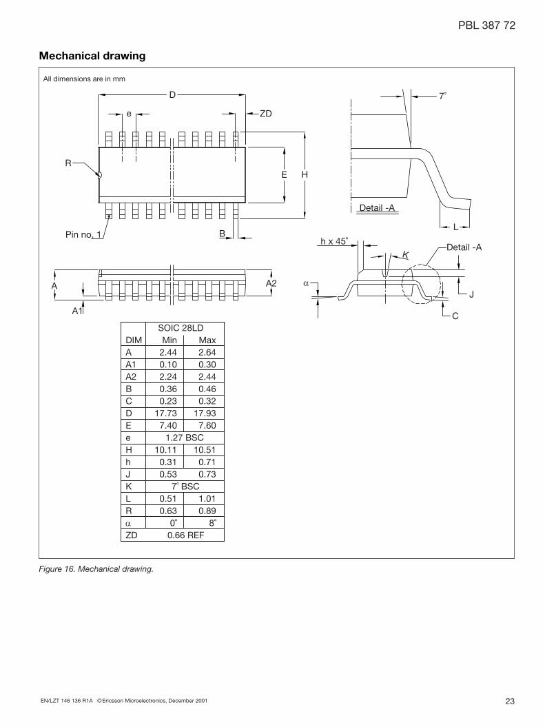
Mechanical drawing
Figure 16. Mechanical drawing.
All dimensions are in mm
D
e
R
ZD
Pin no. 1
E H
Bh x 45˚
A2 α
Detail -A
7˚
L
Detail -A
J
C
K
A
A1
SOIC 28LDDIM Min MaxA 2.44 2.64A1 0.10 0.30A2 2.24 2.44B 0.36 0.46C 0.23 0.32D 17.73 17.93E 7.40 7.60e 1.27 BSCH 10.11 10.51h 0.31 0.71J 0.53 0.73K 7˚ BSCL 0.51 1.01R 0.63 0.89α 0˚ 8˚ZD 0.66 REF
PBL 387 72
23 EN/LZT 146 136 R1A ©Ericsson Microelectronics, December 2001
Ericsson MicroelectronicsSE-164 81 KISTA, SwedenPhone: +46 8 757 5000www.ericsson.com/microelectronics
For local sales contacts, please refer to our websiteor call: Int. +46 8 757 4700, Fax: +46 8 757 4776
Preliminary Data Sheet
EN/LZT 146 136 R1A© Ericsson Microelectronics AB, January 2002
Information given in this data sheet is believed to be accurate and reliable. However no responsibility is assumed for the consequences of its use nor for any infringement of patents or other rights of third parties which may result from its use. No license is granted by implication or otherwise under any patent or patent rights of Ericsson Microelectronics AB. These products are sold only according to Ericsson Microelectronics general conditions of sale, unless otherwise confirmed in writing.Specifications subject to change without notice. This product is an original Ericsson product protectedby US, European and other patents.
Ordering InformationPackage Temp. Range Part No.28-pin SOIC Tape & Reel -40° - +85° C PBL 387 72/1SOD or SOA