summer-16 examination model answer subject code:...
TRANSCRIPT

MAHARASHTRA STATE BOARD OF TECHNICAL EDUCATION
(Autonomous)
(ISO/IEC - 27001 - 2005 Certified)
SUMMER-16 EXAMINATION Model Answer Subject Code: 17333 Subject Name: Digital Technique
Important Instructions to examiners:
1) The answers should be examined by key words and not as word-to-word as given in the model
answer scheme.
2) The model answer and the answer written by candidate may vary but the examiner may try to
assess the understanding level of the candidate.
3) The language errors such as grammatical, spelling errors should not be given more Importance
(Not applicable for subject English and Communication Skills).
4) While assessing figures, examiner may give credit for principal components indicated in the
Figure. The figures drawn by candidate and model answer may vary. The examiner may give
Credit for any equivalent figure drawn.
5) Credits may be given step wise for numerical problems. In some cases, the assumed
Constant values may vary and there may be some difference in the candidate’s answers and
model answer.
6) In case of some questions credit may be given by judgment on part of examiner of relevant
answer based on candidate’s understanding.
7) For programming language papers, credit may be given to any other program based on
Equivalent concept.
Marks
1. a) Attempt any six of the following: 12
i) List the applications of digital systems. 2
(Any two applications - 1 mark each)
Ans:
Applications of digital systems:
1. Television
2. Communication Systems
3. Radar, Navigation & Guidance Systems
4. Medical Systems
5. Military Systems
6. Industrial Process, Control & Automation
7. Consumer Electronics

MAHARASHTRA STATE BOARD OF TECHNICAL EDUCATION
(Autonomous)
(ISO/IEC - 27001 - 2005 Certified)
SUMMER-16 EXAMINATION Model Answer Subject Code: 17333 Subject Name: Digital Technique
ii) Define the following terms. 2
1) Noise Immunity 2) Propogation Delay
(Each Definition -1mark)
Ans:
1) Noise Immunity: The ability of a digital circuit to tolerate noise signals is called as
noise immunity of a circuit
2) Propogation delay: Propagation delay is the average transition delay time for the
signal to propagate from input to output when the signals change in value. It is
expressed in ns.
iii) Draw logical symbol and truth table of X-NOR gate. 2
(Logical Symbol - 1 mark; Truth table - 1 mark)
Ans:
Truth Table of X-NOR Gate:
INPUTS OUTPUT
A B Y
0 0 1
0 1 0
1 0 0
1 1 1

MAHARASHTRA STATE BOARD OF TECHNICAL EDUCATION
(Autonomous)
(ISO/IEC - 27001 - 2005 Certified)
SUMMER-16 EXAMINATION Model Answer Subject Code: 17333 Subject Name: Digital Technique
iv) Which are the universal gates? Why they called it? 2
(Naming - 1 mark; Reason - 1 mark)
Ans:
NAND and NOR gates are called as Universal gates.
With the help of NAND and NOR gates only all basic logical operations can be
constructed, hence they are called as universal gates
v) Convert (268.75)10 = (?)2. 2
(1- mark for integer; 1- mark for decimal correct answer)
Ans:
vi) Give the examples of associative and distributive law of Boolean algebra. 2
(Example of each - 1 mark)
MAHARASHTRA STATE BOARD OF TECHNICAL EDUCATION
(Autonomous)
(ISO/IEC - 27001 - 2005 Certified)
SUMMER-16 EXAMINATION Model Answer Subject Code: 17333 Subject Name: Digital Technique
Ans:
Associative Law
1. (A.B)C=A.(B.C)
2. (A +B)+C= A+ (B+C)
Distributive Law
1. A.B+A.C=A(B+C)
2. (A+B)(A+C)=A+BC
vii) Name the IC for digital comparator and ALU. 2
(Each correct IC name - 1 mark)
Ans:
1. Digital Comparator: IC 7485
2. ALU: IC 74181
viii) Define any two specifications of DAC. 2
(Any two specification of DAC - 1 mark each)
Ans:
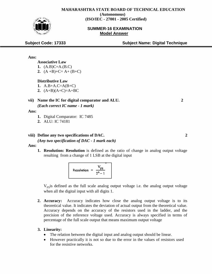
1. Resolution: Resolution is defined as the ratio of change in analog output voltage
resulting from a change of 1 LSB at the digital input
VFSis defined as the full scale analog output voltage i.e. the analog output voltage
when all the digital input with all digits 1.
2. Accuracy: Accuracy indicates how close the analog output voltage is to its
theoretical value. It indicates the deviation of actual output from the theoretical value.
Accuracy depends on the accuracy of the resistors used in the ladder, and the
precision of the reference voltage used. Accuracy is always specified in terms of
percentage of the full scale output that means maximum output voltage
3. Linearity:
The relation between the digital input and analog output should be linear.
However practically it is not so due to the error in the values of resistors used
for the resistive networks.

MAHARASHTRA STATE BOARD OF TECHNICAL EDUCATION
(Autonomous)
(ISO/IEC - 27001 - 2005 Certified)
SUMMER-16 EXAMINATION Model Answer Subject Code: 17333 Subject Name: Digital Technique
4. Temperature sensitivity:
The analog output voltage of D to A converter should not change due to changes
in temperature.
But practically the output is a function of temperature. It is so because the
resistance values and OPAMP parameters change with changes in temperature.
5. Settling time:
The time required to settle the analog output within the final value, after the
change in digital input is called as settling time.
The settling time should be as short as possible.
6. Long term drift
Long term drift are mainly due to resistor and semiconductor aging and can
affect all the characteristics.
Characteristics mainly affected are linearity, speed etc.
7. Supply rejection
Supply rejection indicates the ability of DAC to maintain scale, linearity and other
important characteristics when the supply voltage is varied.
Supply rejection is usually specified as percentage of full scale change at or near
full scale voltage at 25oe
8. Speed:
It is defined as the time needed to perform a conversion from digital to analog. It
is also defined as the number of conversions that can be performed per second
MAHARASHTRA STATE BOARD OF TECHNICAL EDUCATION
(Autonomous)
(ISO/IEC - 27001 - 2005 Certified)
SUMMER-16 EXAMINATION Model Answer Subject Code: 17333 Subject Name: Digital Technique
Page 6 of 38
b) Attempt any two of the following: 8
i) Compare CMOS and TTL logic families on following parameters. 4
1) Propagation Delay 2) Fan-out
3) Speed-power Product 4) Noise Immunity
(1 - mark for each correct parameter)
Ans:
Parameter TTL CMOS
Propagation Delay 10ns 70ns
Fan Out 10 20 -50
Speed power product 100pJ 0.7pJ
Noise Immunity Very good Excellent
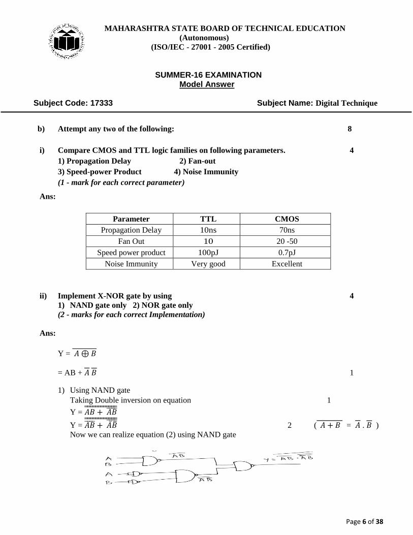
ii) Implement X-NOR gate by using 4
1) NAND gate only 2) NOR gate only
(2 - marks for each correct Implementation)
Ans:
Y =
= AB + 1
1) Using NAND gate
Taking Double inversion on equation 1
Y =
Y = 2 ( = . )
Now we can realize equation (2) using NAND gate

MAHARASHTRA STATE BOARD OF TECHNICAL EDUCATION
(Autonomous)
(ISO/IEC - 27001 - 2005 Certified)
SUMMER-16 EXAMINATION Model Answer Subject Code: 17333 Subject Name: Digital Technique
Page 7 of 38
2) Using NOR gate
Apply Demorgans theorem to eqn
(2)
Y = ( ( = + )
Y = ----------- (Taking double inversion)
iii) Convert the following : 4
1) (327.89)10 = (?)BCD 2) (237)8 = (?)10
3) (1011001)2 = (?)8 4) (249)10 = (?)2
(1 mark for each correct answer)
Ans:

MAHARASHTRA STATE BOARD OF TECHNICAL EDUCATION
(Autonomous)
(ISO/IEC - 27001 - 2005 Certified)
SUMMER-16 EXAMINATION Model Answer Subject Code: 17333 Subject Name: Digital Technique
Page 8 of 38
2. Attempt any four of the following: 16
a) State and prove De-Morgan’s Theorems. 4
(Theorem - 1 mark each; Proof - 1 mark each)
Ans:
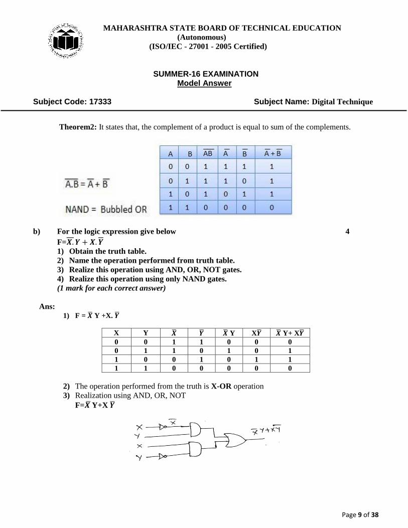
Theorem1: It state that the, complement of a sum is equal to product of its complements
MAHARASHTRA STATE BOARD OF TECHNICAL EDUCATION
(Autonomous)
(ISO/IEC - 27001 - 2005 Certified)
SUMMER-16 EXAMINATION Model Answer Subject Code: 17333 Subject Name: Digital Technique
Page 9 of 38
Theorem2: It states that, the complement of a product is equal to sum of the complements.
b) For the logic expression give below 4
F=
1) Obtain the truth table.
2) Name the operation performed from truth table.
3) Realize this operation using AND, OR, NOT gates.
4) Realize this operation using only NAND gates.
(1 mark for each correct answer)
Ans:
1) F = Y +X.
X Y Y X Y+ X
0 0 1 1 0 0 0
0 1 1 0 1 0 1
1 0 0 1 0 1 1
1 1 0 0 0 0 0
2) The operation performed from the truth is X-OR operation
3) Realization using AND, OR, NOT
F= Y+X

MAHARASHTRA STATE BOARD OF TECHNICAL EDUCATION
(Autonomous)
(ISO/IEC - 27001 - 2005 Certified)
SUMMER-16 EXAMINATION Model Answer Subject Code: 17333 Subject Name: Digital Technique
Page 10 of 38
4)
c) Perform the following subtraction using 2’s complement method. 4
1) (01000)2 – (01001)2 2) (01100)2 – (00011)2
(2 mark for Correct Answer (Step marking can be given))
Ans:

MAHARASHTRA STATE BOARD OF TECHNICAL EDUCATION
(Autonomous)
(ISO/IEC - 27001 - 2005 Certified)
SUMMER-16 EXAMINATION Model Answer Subject Code: 17333 Subject Name: Digital Technique
Page 11 of 38
d) Minimize the following expression using K-map. 4
F(A,B,C,D)= πM(1,4,6,9,10,11,14,15)
(K Map - 1 mark; equation - 2 marks; realization - 1 mark)
Ans:

MAHARASHTRA STATE BOARD OF TECHNICAL EDUCATION
(Autonomous)
(ISO/IEC - 27001 - 2005 Certified)
SUMMER-16 EXAMINATION Model Answer Subject Code: 17333 Subject Name: Digital Technique
Page 12 of 38
e) Design a full adder using half adder. 4
(Designing - 4 marks)
Ans:
Full Adder is a combinational circuit that performs the addition of three bits (two significant bits
and previous carry). It consists of three inputs and two outputs, two inputs are the bits to be added,
the third input represents the carry form the previous position
A B Carry Input SUM
CARRY
OUT
0 0 0 0 0
0 0 1 1 0
0 1 0 1 0
0 1 1 0 1
1 0 0 1 0
1 0 1 0 1
1 1 0 0 1
1 1 1 1 1
A circuit which obeys this truth table is called a full adder. We can design a full adder by linking
together two half adder circuits:
Thus, we can implement a full adder circuit with the help of two half adder circuits. The first will
half adder will be used to add A and B to produce a partial Sum. The second half adder logic can be
used to add CIN to the Sum produced by the first half adder to get the final S output. If any of the
half adder logic produces a carry, there will be an output carry. Thus, COUT will be an OR function
of the half-adder Carry outputs.

MAHARASHTRA STATE BOARD OF TECHNICAL EDUCATION
(Autonomous)
(ISO/IEC - 27001 - 2005 Certified)
SUMMER-16 EXAMINATION Model Answer Subject Code: 17333 Subject Name: Digital Technique
Page 13 of 38
f) Draw the block diagrams of ALU IC 74181 and explain the function of all pins. 4
(Diagram - 2 marks; Blocks Explanation - 2 marks)
Ans:
Arithmetic Logic Unit (ALU):
1. The heart of every computer is an Arithmetic Logic Unit (ALU). This is the part of the
computer which performs arithmetic as well as logical operations .74181 is a 24-pin IC in dual
in line (DIP) package.
2. A (A0-A3) and B (B0-B3) are the two 4 bit variables. It can perform a total of 16 arithmetic
operations which includes addition, subtraction, compare and double operations. It provides
many logic operations such as AND, OR, NOR, NAND, EX-OR, compare, etc. on the two four
bit variables.
3. 74181 is a high speed 4 bit parallel ALU. It is controlled by four function select inputs (S0-S3).
These lines can select 16 different operations for one mode (arithmetic) and 16 another
operations for the other mode (logic).
4. M is the mode control input. It decides the mode of operation to be either arithmetic or logic.
Mode M= 0 for arithmetic operations. M = 1 for logic operations.
5. G and P outputs are used when a number of 74181 circuits are to be used in cascade along with
74182 the look ahead carry generator circuit to make the arithmetic operations faster
6. A=B it is Equality output
7. F (F0-F3) 4-bit binary Data Output
8. Cn: carry input (active-low)
9. Cn+4 carry output (active-low)

MAHARASHTRA STATE BOARD OF TECHNICAL EDUCATION
(Autonomous)
(ISO/IEC - 27001 - 2005 Certified)
SUMMER-16 EXAMINATION Model Answer Subject Code: 17333 Subject Name: Digital Technique
Page 14 of 38
3. Attempt any FOUR of the following: 16
a) Prove the following using the algebraic theorems 4
1) + B+ A =A+B
2) AB + B+ = +B
(2 marks each)
[**NOTE: Steps marks can be given**]
Ans:
1) A+ +A =A+B
L.H.S = A(1) + B + A
= A(1+B)+ B + A (1 + B =1)
= + A + B + A
= B (A + ) + A + A (A+ = 1)
= B (1) +A ( +1)
=B (1) + A (1) ( + 1=1)
=A+B
= R.H.S
= Hence proved.
2) AB + B + = B
L.H.S = AB+ B +
= (B + ) +AB
= + AB (B + =1)
= . (1) + AB
= (1 + B) + AB (1 + B=1)
= + B + AB
= + B ( + A)
= + B (
= R.H.S
Hence Proved

MAHARASHTRA STATE BOARD OF TECHNICAL EDUCATION
(Autonomous)
(ISO/IEC - 27001 - 2005 Certified)
SUMMER-16 EXAMINATION Model Answer Subject Code: 17333 Subject Name: Digital Technique
Page 15 of 38
b) Obtain an 1:8 demultiplexer using 1:4 demultiplexer. 4
(4 marks for correct implementation)
Ans:

MAHARASHTRA STATE BOARD OF TECHNICAL EDUCATION
(Autonomous)
(ISO/IEC - 27001 - 2005 Certified)
SUMMER-16 EXAMINATION Model Answer Subject Code: 17333 Subject Name: Digital Technique
Page 16 of 38
c) Minimize the following function using K-map. 4
F=∑ m (0, 1, 2, 3, 11, 12, 14, 15)
(K-map - 1 mark; Formation of groups - 1 mark; Minimized SOP expression - 1 mark; logic
circuit - 1 mark)
Ans:

MAHARASHTRA STATE BOARD OF TECHNICAL EDUCATION
(Autonomous)
(ISO/IEC - 27001 - 2005 Certified)
SUMMER-16 EXAMINATION Model Answer Subject Code: 17333 Subject Name: Digital Technique
Page 17 of 38
d) Convert F(A,B,C)= ∑m(1,4,5,6,7) in standard POS form. 4
(Conversion - 4 marks)
Ans:
e) Explain the functions of ‘preset’ and ‘clear’ inputs in flip-flops. 4 (Each Input function - 2 marks)
Ans:
The normal data inputs to a flip flop (D, S and R, or J and K) are referred to _
as synchronous inputs because they have effect on the outputs (Q and not Q) only in step, or in
sync, with the clock signal transitions. These extra inputs are called asynchronous because they
can set or reset the flip-flop regardless of the status of the clock signal. Typically, they are
called preset and clear:

MAHARASHTRA STATE BOARD OF TECHNICAL EDUCATION
(Autonomous)
(ISO/IEC - 27001 - 2005 Certified)
SUMMER-16 EXAMINATION Model Answer Subject Code: 17333 Subject Name: Digital Technique
Page 18 of 38
When the preset input is activated, the flip-flop will be set (Q=1, not-Q=0) regardless of any of
the synchronous inputs or the clock. When the clear input is activated, the flip-flop will be reset
(Q=0, not-Q=1), regardless of any of the synchronous inputs or the clock. So, what happens if
both preset and clear inputs are activated? we get an invalid state on the output.
Asynchronous inputs, just like synchronous inputs, can be engineered to be active-high or active-
low. If they’re active-low, there will be an inverting bubble at that input lead on the block
symbol, just like the negative edge-trigger clock inputs.
Sometimes the designations “PRE” and “CLR” will be shown with inversion bars above them, to
further denote the negative logic of these inputs:

MAHARASHTRA STATE BOARD OF TECHNICAL EDUCATION
(Autonomous)
(ISO/IEC - 27001 - 2005 Certified)
SUMMER-16 EXAMINATION Model Answer Subject Code: 17333 Subject Name: Digital Technique
Page 19 of 38
Inputs
OUTPUT
Operation
performed
CLK
PR
CLR
1 1 1 Qn+1 Normal JK
FF
X 0 1 1 FF is set
X 1 0 0 FF is reset
f) Explain 3-bits synchronous counter with truth table and timing diagram. 4 (Diagram - 1 mark; Truth table - 1 mark; Timing diagram - 1 mark; explanation - 1mark)
Ans:
Count 000 001 010 011 100 101 110 111 000
State 0 1 2 3 4 5 6 7 8(0)

MAHARASHTRA STATE BOARD OF TECHNICAL EDUCATION
(Autonomous)
(ISO/IEC - 27001 - 2005 Certified)
SUMMER-16 EXAMINATION Model Answer Subject Code: 17333 Subject Name: Digital Technique
Page 20 of 38
Operation:
Initially all the FFs are in their reset state. QCQBQA=000
1st Clock
pulse:
FF-A toggles and QA becomes 0.Butsince QA = 0 at the instant of application of 1st Falling
clock edge, JB=KB=0 and QB does not change state .
Similarly QC also does not change state
2nd
Clock pulse:
FF-A toggles and QAbecomes 0.
But at the instant of application of 2nd
falling clock edge QA was equal to 1.Hence,
JB=KB=1. Hence FF-B will toggle and QB becomes 1.
Output of AND gate is 0 at the instant of negative clock edge. So JC=KC=0.Hence
QC remains 0.
3rd
clock pulse:
After the 3rd
clock pulse, the output are QCQBQA=011
4th
clock pulse:
Note that QB =QA=1.Henceoutputof AND gate=1andJC=KC=1, at the instant of
application of 4th
negative edge of the clock.
Hence on application of this clock pulse, FF-C will toggle and QC changes from 0 to 1
FF-A toggles as usual and QAbecomes0.
Since QAwas equal to 1 earlier, FF-B will also toggle to make QB=0.
Thus the counting progresses.
After the 7th
clock pulse the output is 111 and after the 8
th clock pulse, all the flip- flops
toggle and change their outputsto0.Hence QCQBQA =000 after the 8th
pulse and the
operation repeats.

MAHARASHTRA STATE BOARD OF TECHNICAL EDUCATION
(Autonomous)
(ISO/IEC - 27001 - 2005 Certified)
SUMMER-16 EXAMINATION Model Answer Subject Code: 17333 Subject Name: Digital Technique
Page 21 of 38
Timing Diagram
4. Attempt any four of the following: 16
a) Distinguish between synchronous and asynchronous counter. 4
(Any 4 each Comparison - 1 mark)
Ans:

MAHARASHTRA STATE BOARD OF TECHNICAL EDUCATION
(Autonomous)
(ISO/IEC - 27001 - 2005 Certified)
SUMMER-16 EXAMINATION Model Answer Subject Code: 17333 Subject Name: Digital Technique
Page 22 of 38
No.
Asynchronous Counter Synchronous Counter
1.
In an Asynchronous Counter the output of
one Flip Flop acts as the clock input of the
next Flip Flop.
In a Synchronous Counter all the Flip Flop’s are
Connected to a common clock signal.
2. Speed is Low Speed is High
3. Only J K or T Flip Flop can be used to
construct Asynchronous Counter
Synchronous Counter can be designed using
JK, RS, T and D Flip Flop.
4. Problem of Glitch arises Problem of Lockout
5. Only serial count either up or down is
possible.
Random and serial counting is possible.
6. Settling time is more Settling time is less
7. Also called as serial counter Also called as Parallel Counter
b) Compare weighted register DAC and R-2R DAC. 4
(Any 4 each Comparison - 1 mark)
Ans:
Weighted resistor DAC R-2 R ladder DAC
It requires more than two resistor values. It requires resistors of only two values.
It is not easy to build. It is easy to build.
It requires one resistor per bit It requires two resistor per bit
It is not possible to expand It can be easily expanded to handle more
number of bits by adding resistors

MAHARASHTRA STATE BOARD OF TECHNICAL EDUCATION
(Autonomous)
(ISO/IEC - 27001 - 2005 Certified)
SUMMER-16 EXAMINATION Model Answer Subject Code: 17333 Subject Name: Digital Technique
Page 23 of 38
c) Draw neat circuit diagram of clocked JK flip - flop using NAND gates. Give its truth table
and explain race around condition. 4
(Diagram - 1 mark; Truth Table - 1 mark; Explanation - 2 marks)
Ans:
Race around condition:
When JK flip flop when the value of J and K =1 and at the same time value of clock is 1 ,so
according to the truth table of J=k=1 the value of output should be toggled so the value keep on
changing till the change in the clock pulse which is not acceptable .
Elimination of Race around Condition: Race around condition can be avoided using Master Slave
Flip flop & by using Edge Triggered Flip Flop
MAHARASHTRA STATE BOARD OF TECHNICAL EDUCATION
(Autonomous)
(ISO/IEC - 27001 - 2005 Certified)
SUMMER-16 EXAMINATION Model Answer Subject Code: 17333 Subject Name: Digital Technique
Page 24 of 38
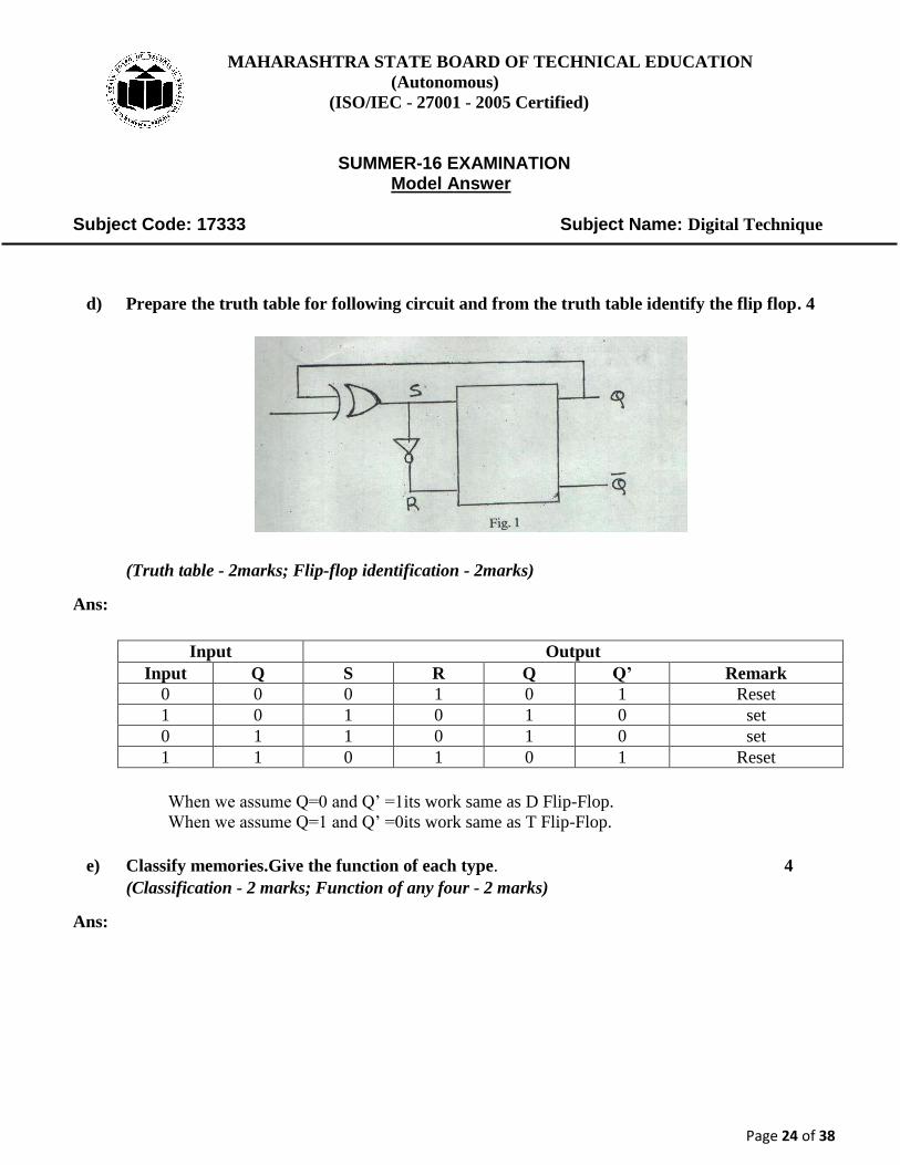
d) Prepare the truth table for following circuit and from the truth table identify the flip flop. 4
(Truth table - 2marks; Flip-flop identification - 2marks)
Ans:
Input Output
Input Q S R Q Q’ Remark
0 0 0 1 0 1 Reset
1 0 1 0 1 0 set
0 1 1 0 1 0 set
1 1 0 1 0 1 Reset
When we assume Q=0 and Q’ =1its work same as D Flip-Flop.
When we assume Q=1 and Q’ =0its work same as T Flip-Flop.
e) Classify memories.Give the function of each type. 4
(Classification - 2 marks; Function of any four - 2 marks)
Ans:
MAHARASHTRA STATE BOARD OF TECHNICAL EDUCATION
(Autonomous)
(ISO/IEC - 27001 - 2005 Certified)
SUMMER-16 EXAMINATION Model Answer Subject Code: 17333 Subject Name: Digital Technique
Page 25 of 38
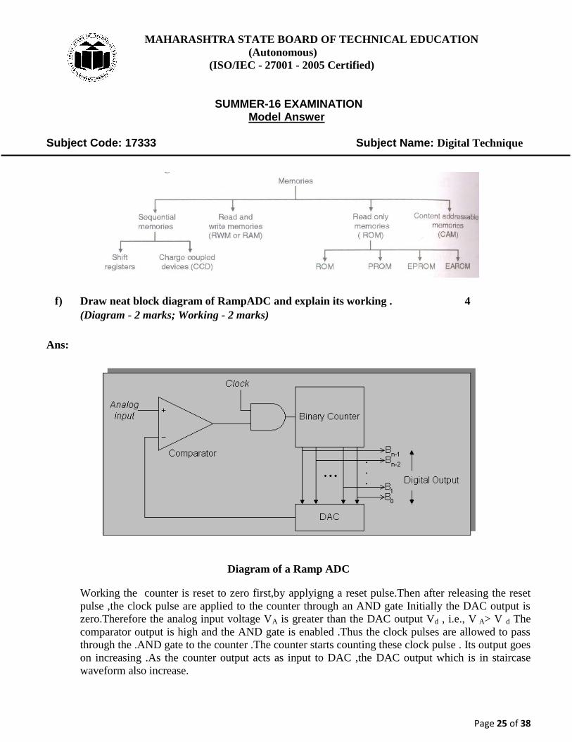
f) Draw neat block diagram of RampADC and explain its working . 4
(Diagram - 2 marks; Working - 2 marks)
Ans:
Diagram of a Ramp ADC
Working the counter is reset to zero first,by applyigng a reset pulse.Then after releasing the reset
pulse ,the clock pulse are applied to the counter through an AND gate Initially the DAC output is
zero.Therefore the analog input voltage VA is greater than the DAC output Vd , i.e., V A> V d The
comparator output is high and the AND gate is enabled .Thus the clock pulses are allowed to pass
through the .AND gate to the counter .The counter starts counting these clock pulse . Its output goes
on increasing .As the counter output acts as input to DAC ,the DAC output which is in staircase
waveform also increase.

MAHARASHTRA STATE BOARD OF TECHNICAL EDUCATION
(Autonomous)
(ISO/IEC - 27001 - 2005 Certified)
SUMMER-16 EXAMINATION Model Answer Subject Code: 17333 Subject Name: Digital Technique
Page 26 of 38
As long as the DAC output vd <vA this process will continue, as the comparator output
remains high enabling the AND gate . howe ver , when the DAC output is high than the input
analog voltage i.e. vd>vA, the comparator output becomes low so that AND gate is disabled and stop
the clock pulse i.e. counting stops . thus the digital output of the counter represents the anolog input
voltage vA. when the anolg input change to a new value ,a second reset pulse is applied to the
counter to clear it againg the counting starts.
5. Attempt any four of the following: 16
a) Perform the following using 9’s complement. 4
1) (52)10-(89)10 2) (83)10-(21)10
(2 marks each)
Ans:
MAHARASHTRA STATE BOARD OF TECHNICAL EDUCATION
(Autonomous)
(ISO/IEC - 27001 - 2005 Certified)
SUMMER-16 EXAMINATION Model Answer Subject Code: 17333 Subject Name: Digital Technique
Page 27 of 38
b) State different applications of flip-flops. 4
(Any four - 1 mark each)
Ans:
Applications of flip flop
Bounce elimination of key
Memory
Registers
Counters
Delay element

MAHARASHTRA STATE BOARD OF TECHNICAL EDUCATION
(Autonomous)
(ISO/IEC - 27001 - 2005 Certified)
SUMMER-16 EXAMINATION Model Answer Subject Code: 17333 Subject Name: Digital Technique
Page 28 of 38
c) Find the Boolean expression for logic circuit given below and reduce it using Boolean algebra.
(Expression - 2 marks; Reducing - 2 marks)
Ans:

MAHARASHTRA STATE BOARD OF TECHNICAL EDUCATION
(Autonomous)
(ISO/IEC - 27001 - 2005 Certified)
SUMMER-16 EXAMINATION Model Answer Subject Code: 17333 Subject Name: Digital Technique
Page 29 of 38
d) Draw and explain SISO with truth table and timing diagram. 4
(Diagram - 1 mark; explanation - 1 mark; truth table - 1 mark; timing diagram - 1 mark)
Ans:
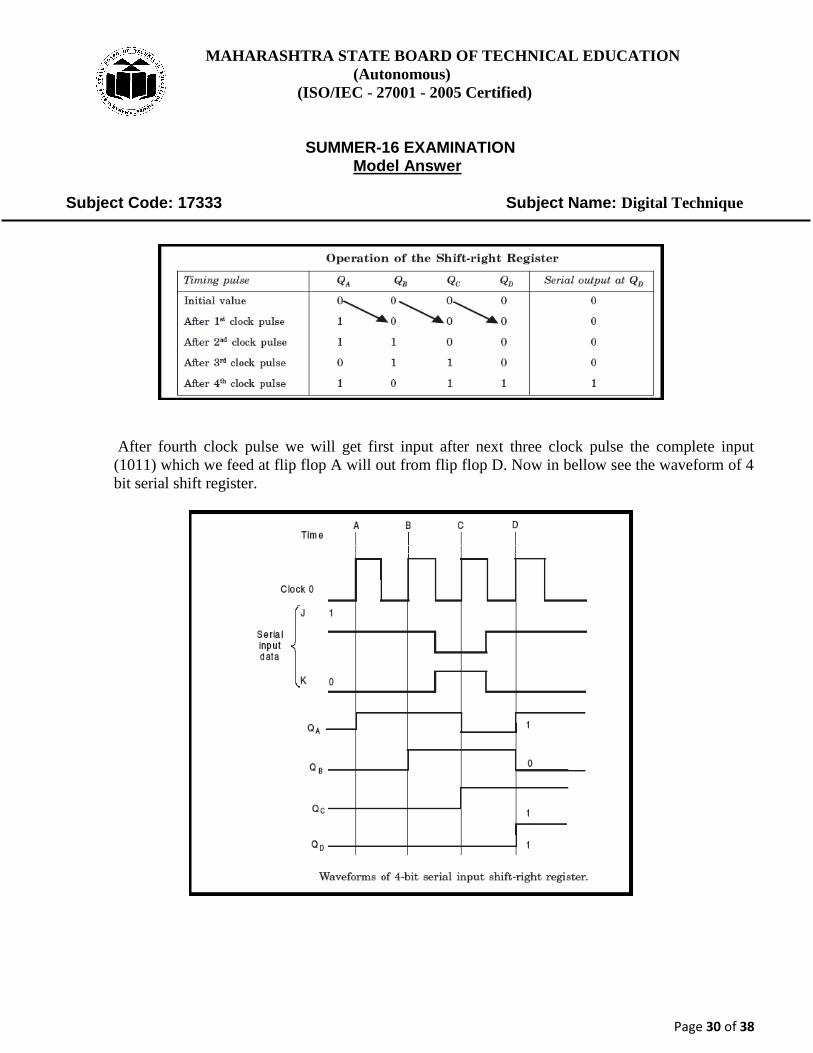
Serial in Serial out Shift Register (SISO), type of shift register accepts data serially, one bit at a
time at the single input line, and shifted to next flip flop serially. The output is also obtained on a
single output line in a same serial fashion.
A shift right register can be constructed with either J-K or D flip flops as shown in below.
As shown in figure J-K flip flop based shift register requires connection of both J and K inputs.
Input data are connected to the J and K inputs of the left most (lowest order) flip flop of flip flop
chain. And all flip flops are connected in serially. For a JK flip flop output is followed whatever
the input of J and the both the input are complimentary. Let take an example to input a 0, one
should apply a 0 at the J input, i.e., J = 0 and K = 1 and vice versa. With the application of a clock
pulse the data will be shifted by one bit to the right. In this way the first data will store at Flip flop
A then in next clock pulse the date of A flip flop is shifted to filp flop B in that way. Finally the
serial output will appear from flip flop D.
For example, consider that all the stages are reset and a logical input 1011 is applied at the serial
input line connected to stage A. the table given below shows how the data is shifted from one flip
flop to other and finally get the output from D flip flop.
MAHARASHTRA STATE BOARD OF TECHNICAL EDUCATION
(Autonomous)
(ISO/IEC - 27001 - 2005 Certified)
SUMMER-16 EXAMINATION Model Answer Subject Code: 17333 Subject Name: Digital Technique
Page 30 of 38
After fourth clock pulse we will get first input after next three clock pulse the complete input
(1011) which we feed at flip flop A will out from flip flop D. Now in bellow see the waveform of 4
bit serial shift register.

MAHARASHTRA STATE BOARD OF TECHNICAL EDUCATION
(Autonomous)
(ISO/IEC - 27001 - 2005 Certified)
SUMMER-16 EXAMINATION Model Answer Subject Code: 17333 Subject Name: Digital Technique
Page 31 of 38
e) Draw the block diagram of BCD to seven segment decoder /driver using IC 7447 with it truth
table 4
(Diagram - 2 marks; truth table - 2 marks)
Ans:

MAHARASHTRA STATE BOARD OF TECHNICAL EDUCATION
(Autonomous)
(ISO/IEC - 27001 - 2005 Certified)
SUMMER-16 EXAMINATION Model Answer Subject Code: 17333 Subject Name: Digital Technique
Page 32 of 38
OR
f) What is modulus of counter? Design a mod - 3 ripple counter using a 2 - bit ripple counter. 4
(Definition - 1 mark; truth table - 1 mark; K map – 1 mark; diagram - 1 mark)
Ans:
Modulus Counter (MOD-N Counter) Modulus of a counter is the no. of different states through which the counter progress during its
operation. It indicates the no. of states in the counter; pulses to be counted are applied to counter.
The circuit comes back to its starting state after counting N pluses in the case of modulus N
counter.

MAHARASHTRA STATE BOARD OF TECHNICAL EDUCATION
(Autonomous)
(ISO/IEC - 27001 - 2005 Certified)
SUMMER-16 EXAMINATION Model Answer Subject Code: 17333 Subject Name: Digital Technique
Page 33 of 38
6. Attempt any two of the following : 16
a) i) Define and draw the logical symbol of demultiplexer. 2
(Definition - 1 mark; diagram - 1 mark)
Ans:

MAHARASHTRA STATE BOARD OF TECHNICAL EDUCATION
(Autonomous)
(ISO/IEC - 27001 - 2005 Certified)
SUMMER-16 EXAMINATION Model Answer Subject Code: 17333 Subject Name: Digital Technique
Page 34 of 38
Demultiplexer: It is a combinational logic circuit which has only one input, n outputs and m select
lines
ii) Realize the logic function of the truth table given below using a multiplexer. 6
(Diagram - 6 mark)
Ans:

MAHARASHTRA STATE BOARD OF TECHNICAL EDUCATION
(Autonomous)
(ISO/IEC - 27001 - 2005 Certified)
SUMMER-16 EXAMINATION Model Answer Subject Code: 17333 Subject Name: Digital Technique
Page 35 of 38
b) i) Draw the symbol and truth table of T flip flop for Negative Edge Triggered. 2
(Symbol - 1 mark; truth table - 1 mark)
Ans:

MAHARASHTRA STATE BOARD OF TECHNICAL EDUCATION
(Autonomous)
(ISO/IEC - 27001 - 2005 Certified)
SUMMER-16 EXAMINATION Model Answer Subject Code: 17333 Subject Name: Digital Technique
Page 36 of 38
ii) List Different types of shift registers. 2
(Any four - ½ mark each)
Ans:
1. Serial input serial output (SISO)
2. Serial input parallel output (SIPO)
3. Parallel input serial output (PISO)
4. Parallel input parallel output (PIPO)
5. Bidirectional Shift Register
6. Universal Shift Register
iii) Compare counters and shift registers. 4
(Any four points - 1 mark each)
Ans:
Parameters Counters Shift register
Flipflop used T flipflop SR, JK flipflop
Modes of operations Serial Up or Down Serial or parallel
Change in output state Output will always follow a
sequence, either in the
upward or downward
direction
Output need not follow
sequence
Types Up Counters
Down counters
Up/ Down counters
Serial input serial
output (SISO)
Serial input parallel
output (SIPO)
Parallel input serial
output (PISO)
Parallel input parallel
output (PIPO)
Bidirectional Shift
Register
Universal Shift
Register
Applications Time and frequency
measurement, clock, ADC
Data shifting

MAHARASHTRA STATE BOARD OF TECHNICAL EDUCATION
(Autonomous)
(ISO/IEC - 27001 - 2005 Certified)
SUMMER-16 EXAMINATION Model Answer Subject Code: 17333 Subject Name: Digital Technique
Page 37 of 38
c) i) With suitable diagram describe successive approximation ADC. 4
(Diagram - 2 marks; Explanation - 2 marks)
Ans:
Successive approximation register
The comparator serves the function of the scale, the output of which is used for setting / resetting
the bits at the output of the programmer. This output is converted into equivalent analog voltage
from which offset is subtracted and then applied to the inverting input terminal of the comparator.
The outputs of the programmer will change only when the clock pulse is present. To start the
conversion, the programmer sets the MSB to 1 and all other bits to O. This is converted into analog
voltage by the DAC and the comparator compares it with the analog input voltage. If the analog
input voltage Va>= Vi, the output voltage of the comparator is HIGH, which sets the next bit also.
On the other hand if Va<= Vi, Then the output of the comparator is LOW which resets the MSB
and sets the next bit. Thus a 1 is tried in each bit of DAC until the binary equivalent of analog input
voltage is obtained.
(ii) List any four specifications of ADC 4
(Any four specifications - 1 mark each)
Ans:
Analog input voltage
Input impedance
Linearity

MAHARASHTRA STATE BOARD OF TECHNICAL EDUCATION
(Autonomous)
(ISO/IEC - 27001 - 2005 Certified)
SUMMER-16 EXAMINATION Model Answer Subject Code: 17333 Subject Name: Digital Technique
Page 38 of 38
Accuracy:
Monotoxicity
Resolution
Conversion Time
Quantization Error
OR
Analog input voltage: This is the maximum allowable input voltage range
Input impedance: Its value ranges from 1 kΩ to 1 MΩ depending upon the type of A/D converter.
Input capacitance is in the range of tens of pF.
Linearity: is conventionally equal to the deviation of the performance of the converter from a best
straight line.
Accuracy: the accuracy of the A/D converter depends upon the accuracy of maximum deviation of
the digital output from the ideal linear line.
Monotoxicity: In response to a continuously increasing input signal the output of an A/D converter
should not at any point decrease or skip one or more codes. This is called the monotoxicity of A/D
converter.
Resolution is define as the maximum number of digital output codes. This is same as that of a DAC
Resolution= 2n Resolution is defined as the ratio of change in the value of the input analog voltage VA, required to
change the digital output by 1 LSB.
Conversion Time: It is the total time required to convert the analog input signal into a
corresponding digital output.
Quantization Error: This approximation process is called as quantization and the error due to the quantization process is
called as quantization error.