supertex inc. hv1 high voltage output hysteretic mode step ... filedoc.# dsfp-hv9150 nr031914...
TRANSCRIPT
Supertex inc. HV9150
Supertex inc. www.supertex.com
Doc.# DSFP-HV9150NR031914
Features ► Wide output voltage range: 6V to 500V ► Low input voltage: 2.7V ► 5W maximum output power with external MOSFET
driver ► Built-in charge pump converter for the gate driver ► Programmable switching frequency from 40kHz to
400kHz ► Four programmable duty cycles from 50% to 87.5% ► FB return ground switch for power savings
applications ► Built-in delay timer for internal protection ► Non-isolated DC/DC converter ► Processed with HVCMOS® technology
Applications ► Portable electronic equipment ► MEMS ► Printers
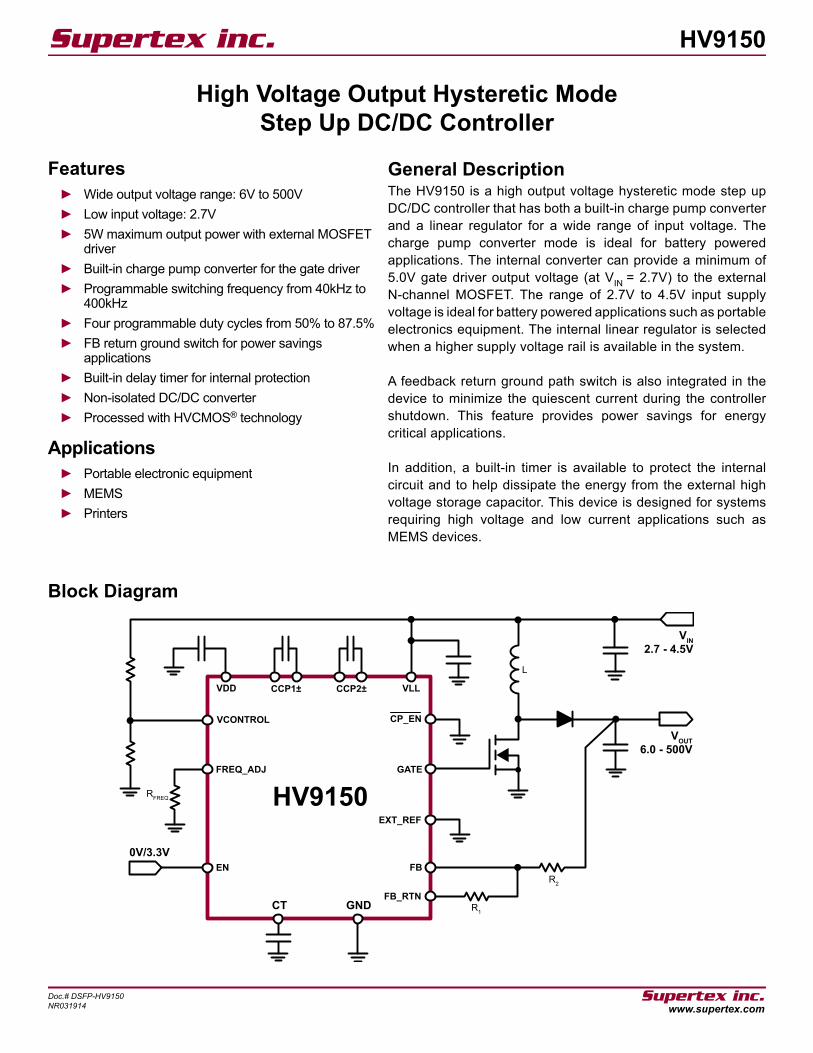
General DescriptionThe HV9150 is a high output voltage hysteretic mode step up DC/DC controller that has both a built-in charge pump converter and a linear regulator for a wide range of input voltage. The charge pump converter mode is ideal for battery powered applications. The internal converter can provide a minimum of 5.0V gate driver output voltage (at VIN = 2.7V) to the external N-channel MOSFET. The range of 2.7V to 4.5V input supply voltage is ideal for battery powered applications such as portable electronics equipment. The internal linear regulator is selected when a higher supply voltage rail is available in the system.
A feedback return ground path switch is also integrated in the device to minimize the quiescent current during the controller shutdown. This feature provides power savings for energy critical applications.
In addition, a built-in timer is available to protect the internal circuit and to help dissipate the energy from the external high voltage storage capacitor. This device is designed for systems requiring high voltage and low current applications such as MEMS devices.
Block Diagram
High Voltage Output Hysteretic ModeStep Up DC/DC Controller
CCP2±
RFREQ
VOUT6.0 - 500V
VIN2.7 - 4.5V
GND R1
R2
L
CT
CCP1±VDD VLL
CP_EN
GATE
EXT_REF
FB_RTN
FBEN
FREQ_ADJ
VCONTROL
0V/3.3V
HV9150

2
HV9150
Supertex inc. www.supertex.com
Doc.# DSFP-HV9150NR031914
Absolute Maximum Ratings*
* All voltages referenced to device GND.
Stresses beyond those listed under “Absolute Maximum Ratings” may cause permanent damage to the device. These are stress ratings only, and functional operation of the device at these or any other conditions beyond those indicated in the operational sections of the specifications is not implied. Exposure to absolute maximum rating conditions for extended periods may affect device reliability.
Parameter Value
VLL, Input voltage supply -0.5V to 5.0V
VDD, Charge pump output voltage -0.5V to 13.6V
Logic input levels -0.5V to VLL +0.5V
Continuous power dissipation(Note: on a 3” by 4” FR4 PCB @Ta = 25°C) 3000mW
Junction temperature range -25°C to +125°C
Storage temperature range -65°C to +125°C
Ordering InformationPart Number Package Option Packing
HV9150K6-G 16-Lead (3x3) QFN 3000/Reel
Pin Configuration
Product Marking
16-Lead QFN
16-Lead QFN(top view)
Package may or may not include the following marks: Si or
Typical Thermal Resistance
Package θja
16-Lead QFN 33°C/W
XFF
ICVG
HDaTVP
HD
XEQPVTQN"
HTGSaCFL
GZVaTGH
EV
XNN
IPF
GP
ERaGP
EER3/
EER3-
EER4/
EER4-
1
16
H 1 5 0Y W L L
Y = Last Digit of Year SealedW = Code for Week SealedL = Lot Number = “Green” Packaging
Symbol Parameter Min Typ Max Units ConditionsVLL Input voltage (CP mode) 2.7 - 4.5 V ---
VIH High-level input voltage 0.8VLL - VLL V ---
VIL Low-level input voltage 0 - 0.2VLL V ---
Recommended Operating Conditions
Power-Up and Power-Down Sequence Power-up sequence should be the following:
1. Connect ground.2. Apply VIN.3. Set all inputs to a known state.
Power-down sequence should be the reverse of the above.
-G denotes a lead (Pb)-free / RoHS compliant package
Note: Pads are at the bottom of the package. Center heat slug is at ground potential.

3
HV9150
Supertex inc. www.supertex.com
Doc.# DSFP-HV9150NR031914
Sym Description Min Typ Max Unit Conditions
Power SupplyILLQ(off) Quiescent VLL supply current (EN = ”0”) - - 2.0 μA ---
ILL(on)
VLL supply current(EN = ”1”)
GATE = NC - - 1.5mA fOSC = 100kHz, VLL = 4.5V
GATE = 300pF - - 4.0
IDD(on)
VDD supply current (EN = ”1”)
GATE = NC - - 1.0mA fOSC = 100kHz, VDD = 12.6V
GATE = 300pF - - 2.5
IDDQ(off) Quiescent VDD supply current (EN = ”0”) - - 2.0 μA ---
IIH High-level logic input current - - 1.0 μA VIH = VLL
IIL Low-level logic input current - - -1.0 μA VIL = 0V
GATE GATE driver output voltage
VLL = 4.5V GATE = NC 10.2 - 12.3
V ---VLL = 2.7VGATE = NC 5.0 - 6.9
VLL(LDO) Linear regulator output voltage 3.0 - 3.6 V ---
AC Electrical Characteristics(Over recommended operating supply voltages and temperatures unless otherwise noted, TJ = 25oC)
Sym Description Min Typ Max Unit Conditions
Feedback (FB)
VREFInternal feedback reference voltage
Accuracy 1.22 1.25 1.28V
---
Range 1.20 1.25 1.30 Tj = -25 to 85°C
IBIAS Input bias current - - 1.0 μA EXT_REF is selected
EXT_REF External reference voltage
Range 0 - VLL-1.4 V ---Trigger INT reference 0 - 0.12 V
During EN positive triggeringTrigger EXT
reference 0.5 - VLL-1.4 V
FB_RTNON-resistance, RDS - - 500 Ω IO = 2.0mA
Breakdown voltage, BV - - 13.5 V ---
GATE Driver Output (GATE)tR Rise time - - 36 ns
CL = 300pF, VDD = 12VtF Fall time - - 12 ns
RUP Pull up resistanceVDD = 5.0V - - 45
ΩIO = 20mA
VDD = 12V - - 30 IO = 50mA
RDOWN Pull down resistanceVDD = 5.0V - - 15
ΩIO = 20mA
VDD = 12V - - 12 IO = 50mA
DC Electrical Characteristics (Over recommended operating supply voltages and temperatures unless otherwise noted, TJ = 25oC)

4
HV9150
Supertex inc. www.supertex.com
Doc.# DSFP-HV9150NR031914
Sym Description Min Typ Max Unit Conditions
fGATE Oscillator frequency - ½ fOSC - kHz ---
Charge Pump Converter
VDD Charge pump output voltage 5.0 3VLL-1.8 12.6 V
2.7V ≤ VLL ≤ 4.5VCCP1 = 220nFCCP2 = 220nFCCP3 = 220nF
fOSC Oscillator frequencyAccuracy 170 195 220
kHzRFREQ = 270kΩ, VLL = 3.3V
Range 40 - 400 Over RFREQ range
Δf Oscillator frequency tolerance - 15 - % 50kHz ≤ fOSC ≤ 250kHz
DC Duty cycle
Accuracy 86 87.5 89 % RFREQ = 270kΩ
Range
- 0 - % 0< VCNTL ≤ 0.18VLL
- 50 - % 0.22VLL < VCNTL ≤ 0.38VLL
- 62.5 - % 0.42VLL < VCNTL ≤ 0.58VLL
- 75 - % 0.62VLL < VCNTL ≤ 0.78VLL
- 87.5 - % 0.82VLL < VCNTL ≤ VLL
VCONTROL Duty cycle adjustment 0 - VLL V See table
RFREQ Frequency adjustment resistor 120k - 1.2M Ω ---
RCPMaximum charge pump output resistance
Pull up - - 20Ω VLL = 2.7V, IO = 10mA
Pull down - - 20
VRIPPLE Output ripple at VDD - - 100 mV
2.7V ≤ VLL ≤ 4.5VfOSC = 200kHzCCP1 = 220nFCCP2 = 220nFCCP3 = 220nFCGATE = 300pFBW = 20MHz
Delay TimerTDELAY Shutdown delay timer - 240 - ms CT = 1.0μF
AC Electrical Characteristics(Over recommended operating supply voltages and temperatures unless otherwise noted, TJ = 25oC)

5
HV9150
Supertex inc. www.supertex.com
Doc.# DSFP-HV9150NR031914
Functional Block Diagram
Delay
OSC
3x Charge PumpConverter LDO
VREF
- +
Hysteretic ModeController
VDD
VDDVLL
VLL
VLL
VLL
CCP1+/- CCP2+/-VDD VLL
GNDCT
EN
FREQ_ADJ
VCONTROL(Duty Cycle Adj)
CP_EN
GATE
EXT_REF
FP_RTN
FB
LDOMode
CPMode
Functional Description Hysteretic Mode ControllerA hysteretic mode controller consists of an oscillator, a voltage reference, a comparator and a driver. Both the internal oscillator and the duty cycle of the gate driver are running at a fixed rate.
As this device is designed for a step up conversion, a pulse train is used to control the switch of a classical switching boost converter. The pulse train is gated by the output of the comparator, which compares the feedback of the output voltage with the voltage reference.
If the output voltage reaches the target voltage, the comparator will turn off the pulse train. When the output voltage drops below the target voltage, the comparator will pass the pulse train to the switch and start the inductor charging cycle. The advantage of this hysteretic mode controller is its stability and simple operation.
Hysteretic Mode Controller and a Classical Boost Converter
Internal OscillatorThis device has an internal oscillator which generates the reference clock for the hysteretic mode controller. The controller is running at half of the frequency of the internal oscillator. This oscillator is powered by the VLL power supply pin.
XQWVXKP
J{uvgtgvke"OqfgEqpvtqnngt

6
HV9150
Supertex inc. www.supertex.com
Doc.# DSFP-HV9150NR031914
The frequency of the oscillator is set by the external resistor RFREQ, and this frequency is inversely proportional to the value of RFREQ. Its characteristic is shown in the fOSC vs RFREQ diagram.
fOSC = 1
4 • RFREQ • C
where C = 4.75pF
Voltage Reference (VREF)The voltage reference is used by the comparator to compare with the feedback voltage and the boost converter output. This device provides the options of using either its internal voltage reference or an external voltage reference.
The internal voltage reference provides a stable 1.25V with a tolerance of ±2.5%. With the use of ±1% tolerance feedback resistors, the output can be achieved with a tolerance of ±4.5%. In order to use the internal voltage reference, the EXT_REF pin must be connected to ground.
If the output voltage of the boost converter is required to have high precision and tight tolerance, the external voltage reference can be used to achieve that purpose. The external reference voltage must be between 0.5V and VLL -1.4V, and connect to the EXT_REF pin. A single low to high transition must be presented at the EN pin to trigger the device to select an external voltage reference. If no enable control signal is available in the application, this signal can be easily mimicked by a simple RC circuit.
Voltage Connection Reference
Gate Driver (GATE)The MOSFET gate driver of this controller is specially designed to be able to drive the gate of the external MOSFET up to 12V. A high pulse voltage will help to minimize the ON-resistance of the external MOSFET transistor. A lower ON-resistance improves the overall efficiency and heat dissipation.
This gate driver is powered by the supply voltage VDD which can be generated by either the internal charge pump converter (CP mode) or the external power supply (LDO mode), depending on the available voltage supply rail of the application.
Charge Pump Converter (CP mode)A 3x charge pump converter is integrated into this device to provide a 5V to 12V rail for the gate driver. It can be activated by setting CP_EN to ground. A 3.3V supply is more common and easily available for digital logic systems; however, this voltage level is less desirable for driving a high voltage MOSFET to obtain a lower ON-resistance for better efficiency.
In order to reduce the number of supply rails used in the system, an internal two stage charge pump converter is added, which can boost the 3.3V supply voltage to 8.0V. A 8.0V gate driver output will outperform a 3.3V gate driver by far and substantially improves the ON-resistance of the external MOSFET.
The charge pump input can operate with an input voltage from 2.7V to 4.5V. Its input and output are connected to the VLL and VDD pins, respectively.
Three Times (3X) Charge Pump Converter
Linear Regulator (LDO mode)In some applications, efficiency may be a key factor, and higher voltage rails such as 5V, 6V, 9V or 12V may be available in the system. The internal charge pump converter cannot operate with these voltage levels because of the maximum output voltage limit of the charge pump converter. At the same time, these voltage levels are high enough to provide an adequate supply for the gate driver.
Under this circumstance, an internal linear regulator is used to replace the charge pump converter. This linear regulator input can accept voltage from 5.0V to 12.0V, and generates a 3.3V output to supply to the internal circuit. This linear regulator can be activated by setting CP_EN to VLL.
In a scenario when the device is operating in LDO mode and in shutdown state (EN = ”0”), the voltage at VLL is undefined. In order to wake up the controller device, a voltage above 2.7V has to be presented at the enable pin (EN).
FB Ground Return Switch (FB_RTN)Any DC/DC controller requires a feedback from the output to monitor its operation so that it can regulate its output accordingly. A simple resistor network is used in conjunction with a feedback ground switch as a feedback path. The purpose of this feedback ground switch is to save power consumed by the feedback resistor network when the controller is disabled. This function is quite useful for power saving especially for battery operated applications.
XFFXNN
QUE
GND
VIN
EXT_REF EXT_REF
GNDVoltageReference
Internal External
7
HV9150
Supertex inc. www.supertex.com
Doc.# DSFP-HV9150NR031914
Shutdown Timer and Timing Capacitor (CT)A shutdown timer is also integrated into the controller for safety purposes. When the controller shuts down from its normal operation, the converter initial output is still at its high level. If the feedback ground return switch is disabled at the same time, a current path is created from the output via the feedback resistor, and the internal protection clamping diode at the FB pin. Depending upon the value of the FB resistor, this momentarily conducting current can be high enough to damage this clamping diode. In order to avoid this potential problem, a timer is added to the disable function to keep the feedback ground switch to the on position for a short period of time. This on time duration is controlled by an external capacitor CT. The larger the capacitor value is, the longer this on time is. Its characteristic is shown in the performance section.
Internal Protection Diode at FB Pin
Hysteretic Controller Enable (EN)The controller enable pin (EN), serves two main purposes. The most obvious function is to turn the controller on and off, and the other function is to act as a trigger to activate the device to accept external voltage reference.
For any applications required a highly precise voltage reference, an external voltage reference should be used. To activate the device to accept the external voltage reference, a low to high transition has to appear at the EN pin while the voltage at the EXT_REF pin is above 0.5V.
If the system lacks enable function control, a RC circuit can be used to mimic this function to allow the external voltage reference.
Simple RC Circuit for EN Pin
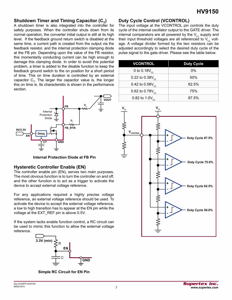
Duty Cycle Control (VCONTROL)The input voltage at the VCONTROL pin controls the duty cycle of the internal oscillator output to the GATE driver. The internal comparators are all powered by the VLL supply and their input threshold voltages are all referenced to VLL volt-age. A voltage divider formed by the two resistors can be adjusted accordingly to select the desired duty cycle of the pulse signal to the gate driver. Please see the table below.
VCONTROL Duty Cycle
0 to 0.18VLL 0%
0.22 to 0.38VLL 50%
0.42 to 0.58VLL 62.5%
0.62 to 0.78VLL 75%
0.82 to 1.0VLL 87.5%VOUT
0V/3.3VDelay
CT GND
FB_RTN
FB
EN
R2
R1
InternalProtection
Diode
GND
EN
3.3V (min)R
C
+-
+-
+-
+-
Duty Cycle 87.5%
VCONTROL
VLLVLL
Duty Cycle 75.0%
Duty Cycle 62.5%
Duty Cycle 50.0%

8
HV9150
Supertex inc. www.supertex.com
Doc.# DSFP-HV9150NR031914
Design ProcedureThere are several parameters that a user will decide for the DC/DC converter design. The input voltage, output voltage and output power requirement are usually defined at the beginning. The few parameters that the user needs to decide on include: operating frequency, inductor value, duty cycle and the ON-resistance of the MOSFET. There is some degree of flexibility in deciding the values of these parameters. The following provides the user a general approach to this subject.
Step 1Since this DC/DC controller device is operating in a discontinuous conduction mode, the following equations are used to determine the inductance and the switching frequency.
Given: D = duty cycle R = load resistance of the high voltage output Vi = minimum input voltage VO = output voltage
Unknown: L = inductance fGATE = driver switching frequency
where:
K = 2 • L • fGATE
R
The maximum duty cycle can be determined by the following equation: DMAX = 1 -
Vi
Vo
Then, the user can choose any duty cycle less than DMAX. It is recommended that the largest possible setting be chosen.
To compensate for the limited efficiency, the user can add the efficiency factor into the load resistance R. With the above equation, the product of L and fGATE is determined. The design will be limited by the product of L and fGATE.
Step 2The standard inductor is usually sold in an incremental inductance value, for example, 10, 22, 33 or 47µH. The user can choose the inductance based on the size of the inductor, the peak current, the maximum operating frequency and the DC resistance. After the value of L is decided, the gate driver
switching frequency can be computed. The required RFREQ resistance can be found in the fGATE vs RFREQ table. Next, the peak current of the inductor is checked by the following equation. The saturation current of the inductor must be larger than IPEAK.
IPEAK = Vi • D
L • fGATE
Step 3The most important factors to determine the MOSFET are the breakdown voltage, the current capability, the ON-resistance, the minimum VGS threshold voltage and the input capacitance.
The HV9150 gate driver is designed to drive a maximum of 300pF capacitive load. So, the maximum input capacitance of the external MOSFET should be less than 300pF. The minimum breakdown voltage must be larger than the required DC/DC converter output voltage. If the breakdown voltage is too low, the output will never reach the required voltage output. A MOSFET with high ON-resistance will limit the peak current charging the inductor. The user can use a simple RL charging circuit equation to determine its final charging current.
It is recommended that the calculated value of IL is within 95% of the IPEAK calculated in step 2. An ON-resistance of less than 1Ω is usually a good starting point.
If the final circuit is short on the output current capability, there are a few ways to boost the output. The user can do any or all of the following to improve the output: (1) increase the duty cycle (2) decrease the fGATE (3) use a MOSFET with lower ON-resistance.
VO =
Vi • 1 + 1 +
4D2
2 K( (IL =
Vi 1 - exp -
D •
RON
RON
fGATE
L( (

9
HV9150
Supertex inc. www.supertex.com
Doc.# DSFP-HV9150NR031914
Typical Application CircuitsCharge Pump (CP) Mode
Linear Regulator (LDO) Mode
CCP2±0.22µF
RFREQ
VOUT6.0 - 500V
VIN2.7 - 4.5V
GND
R1
R2
L
CT
Delay
OSC
VREF
3x Charge PumpConverter LDO
CCP1±0.22µF
VDD0.22µF
VLL1.0µF
CP_EN
- +
VLL
VLL
VLL
VDD
GATE
EXT_REF
FB_RTN
FB
EN
FREQ_ADJ
VCONTROL
0V/3.3V
VDD
LDOMode
CPMode
CCP2±
RFREQ
VOUT15 - 500V
VIN5.0 - 12V
GND
R1
R2
L
CT
Delay
OSC
VREF
3x Charge PumpConverter LDO
CCP1±VDD VLL
CP_EN
- +
VLL
VLL
VLL
VDD
GATE
EXT_REF
FB_RTN
FB
EN
FREQ_ADJ
VCONTROL
0V/3.3V
VDD
1.0µF
LDOMode
CPMode

10
HV9150
Supertex inc. www.supertex.com
Doc.# DSFP-HV9150NR031914
Typical Performance Characteristics
35
30
25
20
15
10
5
00 50 100 150 200 250 300 350
Tim
e (n
s)
Load Capacitance (pF)
Gate Driver Rise Time (tr) and Fall Time (tf) vs Load Capacitance at 25OC
Rise time tr, VDD = 11V(CP mode)
Fall time tf, VDD = 11V(CP mode)
Rise time tr, VDD = 5V(LDO mode)
Fall time tf, VDD = 5V(LDO mode)
1000
100
1010 100 1000
Freq
uenc
y (k
Hz)
RFREQ (kΩ)
Gate Driver Switching Frequency vs RFREQ(V
IN = 3.3V at 25OC)

11
HV9150
Supertex inc. www.supertex.com
Doc.# DSFP-HV9150NR031914
Typical Performance Characteristics (cont.)
100
10
1.0
0.110 100 1000 10000
Ecrcekvcpeg"*¿H+"
Fgnc{"*ou+
EV"Ecrcekvqt"Xcnwg"xu"Fgnc{"Vkog"cv"47QE
12.0
11.0
10.0
9.0
8.0
7.0
6.0407""""""""""""""""""""""""""""""""""""""""""""502""""""""""""""""""""""""""""""""""""""""""""""507""""""""""""""""""""""""""""""""""""""""""""""602"""""""""""""""""""""""""""""""""""""""""""""607"""""""""""""""""""""""""""""""""""""""""""""702
Ejctig"Rwor"Qwvrwv"Xqnvcig"XFF"*X+
Kprwv"Xqnvcig"XNN"*X+
Ejctig"Rwor"Qwvrwv"Xqnvcig"xu"Kprwv"Xqnvcig"cv"47QE
CL=100pF
CL=220pF
CL=330pF

12
HV9150
Supertex inc. www.supertex.com
Doc.# DSFP-HV9150NR031914
Typical Performance Characteristics (cont.)
12
11
10
9.0
8.0
7.0
6.0
5.00 50 100 150 200 250 300 350
Out
put V
olta
ge V
DD (V
)
Load Capacitance (pF)
Charge Pump Output Voltage vs Load Capacitance at 25OC(f
GATE = 100kHz, C
CP1 = C
CP2 = 0.22µF, C
VDD = 1.0µF)
VLL = 4.5V
VLL = 3.6V
VLL = 3.3V
VLL = 2.7V
101
100
99
98
97
962.0 3.0 4.0 5.0 6.0 7.0 8.0 9.0 10 11 12 13 14
Freq
uenc
y (k
Hz)
VLL Input Voltage (V)
LDO mode
CP mode
Gate Driver Switching Frequency vs VLL Input Voltage(Gate output load capacitance = 330pF, R
FREQ = 255kΩ @ 25OC)

13
HV9150
Supertex inc. www.supertex.com
Doc.# DSFP-HV9150NR031914
Typical Performance Characteristics (cont.)
100
90
80
70
60
50
40
30
20
10
0VCONTROL from Max to Min VCONTROL from Min to Max
Perc
enta
ge o
f VLL
Duty Cycle Selection Hysteresis at VCONTROL Pin at 25OC
82%
62%
42%
22%
78%
58%
38%
18%
87.5% Duty Cycle
75% Duty Cycle
62.5% Duty Cycle
50% Duty Cycle
0% Duty Cycle
87.5% Duty Cycle
75% Duty Cycle
62.5% Duty Cycle
50% Duty Cycle
0% Duty Cycle
VIN = 4.5V
VIN = 2.7V
VCP Noise

14
HV9150
Supertex inc. www.supertex.com
Doc.# DSFP-HV9150NR031914
Switching Waveforms
Enabling to use the External Voltage Reference
Delay Time at FB_RTN
Initial power up
XQWV"*GZVaTGH+
XQWV"*KPVaTGH+
2X
XKJ
XKN
XQWV
GP
tDELAY
2X
2X
XKJ
XKN
XQWV
HDaTVP
GP
Pin DescriptionPin # Function Description
1 VLL Input supply voltage2 GND Ground connection3 EN Enable4 CP_EN Charge pump/LDO enable input5 VCONTROL Duty cycle adjustment voltage control input6 FREQ_ADJ Frequency adjustment7 EXT_REF External reference voltage input8 CT Timing capacitor9 FB Feedback input voltage10 FB_RTN Feedback return11 GATE Gate control output12 VDD Charge pump output voltage13 CCP2+ Charge pump storage capacitor #2 plus terminal14 CCP2- Charge pump storage capacitor #2 minus terminal15 CCP1+ Charge pump storage capacitor #1 plus terminal16 CCP1- Charge pump storage capacitor #1 minus terminal
Center Pad Substrate connection (at ground potential)

Supertex inc. does not recommend the use of its products in life support applications, and will not knowingly sell them for use in such applications unless it receivesan adequate “product liability indemnification insurance agreement.” Supertex inc. does not assume responsibility for use of devices described, and limits its liabilityto the replacement of the devices determined defective due to workmanship. No responsibility is assumed for possible omissions and inaccuracies. Circuitry andspecifications are subject to change without notice. For the latest product specifications refer to the Supertex inc. (website: http//www.supertex.com)
©2014 Supertex inc. All rights reserved. Unauthorized use or reproduction is prohibited. Supertex inc.1235 Bordeaux Drive, Sunnyvale, CA 94089
Tel: 408-222-8888www.supertex.com15
HV9150
(The package drawing(s) in this data sheet may not reflect the most current specifications. For the latest package outline information go to http://www.supertex.com/packaging.html.)
Doc.# DSFP-HV9150NR031914
16-Lead QFN Package Outline (K6)3.00x3.00mm body, 1.00mm height (max), 0.50mm pitch
Symbol A A1 A3 b D D2 E E2 e L L1 θ
Dimension(mm)
MIN 0.80 0.000.20REF
0.18 2.85* 1.50 2.85* 1.500.50BSC
0.20† 0.00 0O
NOM 0.90 0.02 0.25 3.00 1.65 3.00 1.65 0.30† - -
MAX 1.00 0.05 0.30 3.15* 1.80 3.15* 1.80 0.45 0.15 14O
JEDEC Registration MO-220, Variation VEED-4, Issue K, June 2006.* This dimension is not specified in the JEDEC drawing.† This dimension differs from the JEDEC drawing.Drawings not to scale.Supertex Doc.#: DSPD-16QFNK63X3P050, Version A092909.
SeatingPlane
Top View
Side View
Bottom View
A
A1
D
E
D2
e
b
E2
A3 L
L1
View B
View B
1
Note 3
Note 2
Note 1(Index AreaD/2 x E/2)
Note 1(Index AreaD/2 x E/2)
16
1
16
θ
Notes:1. A Pin 1 identifier must be located in the index area indicated. The Pin 1 identifier can be: a molded mark/identifier; an embedded metal marker; or
a printed indicator.2. Depending on the method of manufacturing, a maximum of 0.15mm pullback (L1) may be present.3. The inner tip of the lead may be either rounded or square.