supertex inc. - microchip technologyww1.microchip.com/downloads/en/devicedoc/md2134db1...
TRANSCRIPT

Supertex inc.
Supertex inc. www.supertex.com
MD2134DB1
Doc.# DSDB-MD2134DB1A070114
IntroductionThe MD2134 is a high-speed, arbitrary waveform, push-pull source-driver. It is designed for medical ultrasound imaging and HIFU beam forming applications. It also can be used in NDT, sonar and other ultrasound phase-array focusing beam-forming applications.
The integrated circuit (IC) consists of the CMOS digital logic input circuits, an 8-bit current DAC for the waveform amplitude control, and four pre-stored Sine waveforms with pulse-amplitude-modulation (PAM) current sources. These current sources are constructed with the high-speed current-switch array and SPI programmable LV[15:1] PAM level registers. The PAM level resolution of the waveform is 7-bit, 128-step plus sign. There are four logic inputs M[3:0] as fast control signals. They control the push-pull current-source’s output timing, frequency, cycle in the burst, as well as the current-level output. The 15 level registers, along with the DAC value, together can be written and read-back via a SPI serial interface. The MD2134’s output stage is designed to drive two depletion mode high voltage Supertex DN2625 N-type MOSFETs as the source drivers. The MOSFET drains are connected to a center-tap ultrasound frequency pulse transformer. The secondary winding of the transformer can connect to the ultrasound piezo or capacitive transducer via cable and with a good impedance match. MD2134 has a high-speed 120MHz serial data interface that can quickly update the beam forming apodization between scans.
General DescriptionThis demoboard datasheet describes how to use the MD-2134DB1 to generate the ultrasound transmit beam forming waveform with the Gaussian profile, and the adjustable fre-quency, amplitude and phase angle. It also provides informa-tion about how to design a user application circuit and PCB using the MD2134K7 and DN2625DK6 devices. The MD2134DB1 circuit uses a pair of depletion mode, high voltage, DN2625 MOSFETs in the push-pull mode to drive the center-tap wide band ultrasound output transformer. The MOSFETs are in one 8-Lead DFN surface mount pack-age. The sources of the MOSFETs are directly driven by the MD2134’s two outputs, whose maximum peak sinking current is up to 3.3A. These current-source outputs are controlled by the MD1234’s internal current source switch array and the in-put signals M[3:0]. All of the MD2134’s logic control signals are generated by two small CPLD-programmable logic circuits clocked by an on-board 160MHz crystal oscillator. The on-board CPLD circuits not only generate accurate timing for the high-speed PAM level control waveforms, but also the serial data and clock to set and change the waveform amplitude DAC and waveform selection registers. The external clock input can be used if the on-board oscillator is disabled. The external trigger input can be used to synchronize the burst waveforms’ launch timing.
There are five push buttons for enabling and selecting the out-put waveform selection (PAM), amplitude (DAC) and chip en-
MD2134 UltrasoundBeamforming Transmitter Demoboard
Demoboard Block Diagram
T11:1:1
+70 to 100V VPP
C7 220pF
XDCX
+2.5V+3.3V
OSC
EXTRG
EXCLK
DIS
WaveFreq
PhaseAmplENA
PhaseDACPWREN
160MHz
JTAG
DN2625
1k
LOAD
JUMPDN2625
+5.0V +3.3V
CPLD
VCCIO
EXTRG
CLKIN
ENM1M3M0M2
SDISDOSCK
CSLD
MD2134
PA
PBRFB
VDD
GND
+5.0V +3.3V
+5.0V
VLL
+2.5V
VCC

2
MD2134DB1
Supertex inc. www.supertex.com
Doc.# DSDB-MD2134DB1A070114
able (EN). The FREQ button is not being used for this revision of firmware. Four color LEDs indicate the power, chip enable, waveform selection, and DAC states. The MD2134DB1 output waveform can be displayed by using an oscilloscope and the high impedance probe at the TP13 test point. It also can use an SMA to BNC 50Ω coaxial cable connected directly to an os-cilloscope, with an attenuation of 5:1 if R10 is 200Ω. A cable can also be used to drive the user’s transducer directly. Jumper J4 can be used to select whether or not to connect the on-board equivalent-load, which is formed by a 220pF capacitor in paral-lel with a 1.0kΩ resistor.
Circuit Design & PCB LayoutThe thermal pad at the bottom of the MD2134 package must be connected to the VSUB pin on the PCB. The VSUB is con-nected to the IC’s substrate. It is important to make sure that the VSUB is well grounded. A proper supply voltage power-up sequence is needed to test the circuit. To prevent any sup-ply voltage polarity reversing, the circuit also has protection Schottky diodes (D7, D8 and D9). Due to the high current and high current slew rate nature of this common gate, source-driven and push-pull circuit topol-ogy, the two cascading N-channel MOSFETs need to have very low lead inductance of the connections. The Supertex DN2625DK6 is designed for this application and works with the MD2134K7 seamlessly. In particular, a good PCB layout design needs to shorten the traces between the MD2134K7 output pins and the DN2625DK6 source pins. It is also neces-sary to connect all three pairs of pins between them for the high current carrying capacity. Furthermore, because of the high di/dt current in MD2134’s outputs, it is also necessary to connect the Schottky diodes D5 and D6 from the driver output pins connected to the +5.0V power supply line, as the clamp-ing diodes. Note that the diodes must have enough speed and peak current capability. The RC snubber circuits of R8-C5 and R15-C28 at the output pins can dump the current pulse edge ringing effectively. PCB designers need to pay attention to some of the connect-ing traces as high-voltage and high-speed traces. In particular, low capacitance to the ground plane and more trace spacing needs to be applied in this situation.
High-speed PCB trace design practices that are compatible with about 100 to 200 MHz operating speed are used for the demoboard PCB layout. The internal circuitry of the MD2134 can operate at quite a high frequency, with the primary speed limitation being load capacitance. Because of this high speed and the high transient currents that result when driving even
very small inductive loads, ringing and even oscillations are possible. The supply voltage bypass capacitors and the MOSFET gate de-coupling capacitors should be as close to the pins as possible. The capacitor’s ground pin pads should have low inductance, feed-through connections that are con-nected directly to a solid ground plane. The VDD and VPP supplies can draw fast transient currents of up to 3.5A, so they should be provided with a low-impedance bypass capacitor at the chip’s pins. A ceramic capacitor of 0.1 to 1.0µF may be used. Minimize the trace length to the ground plane, and in-sert a ferrite bead in the power supply lead to the capacitor to prevent resonance in the power supply lines. For applications that are sensitive to jitter and noise and when using multiple MD2134 ICs, insert another ferrite bead between VDD and decouple each chip supply separately. Pay particular attention to minimizing trace lengths and using sufficient trace width to reduce inductance not only on the supply pins but also on the CA/B and KA/B compensation pins. Very closely placed sur-face mount components are highly recommended. Be aware of the parasitic coupling from the high voltage outputs to the input signal terminals of MD2134. This feedback may cause oscillations or spurious waveform shapes on the edges of signal transitions. Since the input operates with signals down to 2.5V, even small coupling voltages may cause problems. Use of a solid ground plane and good power and signal layout practices will prevent this problem. Also ensure that the cir-culating ground return current from a capacitive load cannot react with common inductance to create noise voltages in the input logic circuitry.
This MD2134DB1 demoboard should be powered up with multiple DC power supplies with current limiting functions. The power supply voltages and current limits used in the testing are listed on page 7. There are examples of the MD2134DB1 demoboard input and output waveform and measurements shown in Figures 1 to 7 below.
Output Transformer DesignThe center tap, wide band, ultrasound transformer for push- pull output circuit serves three functions: a balanced-differen-tial to single-end output transformer; an isolation barrier to the ultrasound probe; and an impedance matching or low-pass network combined with the cable and transducer element. The MD2134 PAM clock may operate at a 80 to 160MHz frequen-cy range, however the wide band transformer needs only to work in the frequency band of the dummy load (220pF//1.0k). Besides the bandwidth consideration, the small transformer should be designed using a ferrite magnetic core selected to give high enough saturation current and low leakage induc-tance.

3
MD2134DB1
Supertex inc. www.supertex.com
Doc.# DSDB-MD2134DB1A070114
OU
T1
IN3
OU
T1O
UT2
2 4
3 41
C27 0.
1
WAV 2FRE 3
GND 4
PAM 5
AMPL 6
TDI19TMS 10
TCK 11
VCC
GND 17
M2
20
M1
19
M3
21
M0
18
TDO124
GND 25
VCC
F29
NC1130NC1231
Z22
Y16
VCC
EXTRG39
D40
CLKIN43
X23
V14
U13
ENA 7
EN
12NC1027
L1
A44
K42
M41
J38
B37
N34
C36
G28
E32
H33
I8
U2
XC95
72XL
_VQ
44TP
11
B2
R2
50
PW
R
B3
12345
J7
D1
R27 0
TP5
VG
G
B4
PB
VD
D
PH0
MH
2
MH
3
MH
4
MH
1
B5
VD
D2
3U
4LM
4040
VD
D
B6
EN
VC
C
TP4
123456
J6JT
AG
VC
C
B7
PA
C15
27nF
B8
C24 0.1
B9
C1
0.1
1 2
4 3D6B
43D5B
35 14
67910
2
1
2
7 8 9 10 11 12
M1B
DN
2625
DK
6O
UTP
UT
R15
1.0
1W
R9
100
1W
R14 200
VP
P
B11
SD
I
CS
SC
KS
DO
LD
(+3.
3V)
VG
G
C23
0.1
VD
D
C28
3.3n
F
+
1 2
D4
YLW
R3
1k
DAC
1 2(+
3.3V
)V
GG
VLL
C21
27nF
12J2
EX
= 0
1
23
1 2
VD
D
R1 1k
KA1
GND 2
C1A3
GND 4VDD5
C3A6
GND7
VLL8
DG
ND
9
SC
K10
SD
I11
M3
12
M2
13
M1
14
M0
15
VDD16
AGND 17
SD
O18
CS
19
LD20
EN
21
VREF 22
RFB 23
GND24
C3B25
VDD26
GN
D27
C1B28G
ND
29
KB 30
C2B 31
PB
32P
B33
PB
34
VS
UB
35V
SU
B36
PA37
PA38
PA39
C2A40
VSUB
U1
MD
2134
K7
TP3
(+70
to 1
00V
)V
PP
+C
32 1016
V
1
23J5 X
DC
R- A
16
D8A
C6
0.1
TP13
1
23
R7
50
C2
0.1
J3E
XTR
GJ1E
XC
LK
TP1
R10 200
VC
C
R17 33k
(+3.
3V)
VC
C
C19
220p
250V
EN
PH
0
R13
1k 1W
VC
C
C36
1µ 100V
3
4
5613141516
EN
1
GN
D2
OU
T3
VC
C4
X1
FXO
-HC
73-1
60
43D7B
SD
I
(+5.
0V)
VD
D
16D7A
C12 0.1
21
D9
B11
00-1
3
TP19
SD
O
R16
49.9
k
TP2
TP15
PWR
R11 0
SC
K
1 6
D6A
16
D5A
NC1 2
NC2 3
GND 4
NC3 5
NC4 6
TDI2 9TMS10
TCK 11
VCCIO26
GND 17
NC
820
NC
719
NC
621
NC
918
TDO2 24
GND 25
VCC15
FF29
LED230LED131
SD
I22
SD
O16
VCC
35
EXTRG39
DD
40
CLKIN43
SC
K23
CS
14
LD13
NC5 7
EN
12
PWR27
LL1
AA44
KK
42
MM
41
JJ38
BB37
NN
34
CC
36
GG
28
EE
32
HH
33
II8
U3
XC95
72XL
_VQ
44
CS
EN
DA
C
TP17
B0
R8
1.0
1W
C22 0.
1
D2
C39 0.1
LD
12
34
J4
B1
R18 33k
R19 33k
R20 33k
R21 33k
R22 200
R23 200
R24 200
R25 200
R26 200
SW1
SW2
SW3
SW4
SW5
C30 0.1
C35 0.1
C38 0.1
C37 0.1
C31 0.1
R4
1kR
51k
R6
1k
D1
YLW
D1
RE
DD
3G
RN
TP20
C33
10 16V
C18 1µ
100V
R12
100
1WM
1AD
N26
25D
K6
C5
3.3n
F
C17
0.1
C16 0.1
41
1
C3
0.1
C4
0.1
C14
27nF
C13
27nF
C26
27nF
C25
27nF
TP10
TP14
TP18
TP16
TP6
TP12
TP7
TP9
TP8
B10
B2
B3
B4
B5
B6
B7
B8
B9
B11
B0
B1
B10
C8
0.1
C7
0.1
VC
C
C9
0.1
152635
C11 0.1
C10 0.1
C29 0.1
VLL
T1E
P10
_EP
13
C20
0.1
U5
AD
P333
9AK
C-2
.5R
L7
VC
C(+
2.5V
)V
LL
C34 10
16V
+
R28 0
D8B
TP1
Circuit Schematic

4
MD2134DB1
Supertex inc. www.supertex.com
Doc.# DSDB-MD2134DB1A070114
PCB Layout
Actual Dimensions: 10.2cm x 7.6cm (4.00” x 3.00”)
MD2134DB1 Demoboard

5
MD2134DB1
Supertex inc. www.supertex.com
Doc.# DSDB-MD2134DB1A070114
Figure 1: Output waveform of 16-sample/cycle fS = 160MHz, VPP = 75V, 220pF//1.0kΩ load.LV = (0, -12, -12, -45, -45, -12, -12, 0, 0, 14, 14, 45, 45, 14, 14, 0, . . .) 5 cycles
MD2134DB1 Input and Output Waveforms
DAC
A
B
DGND AGND
C3A KA C1A
C3B C2B C1BVREF
+VREF
M0
M1
M2
M3
EN
SDI
SDO
SCK
CS
LD
VLL
SUB DataLatch
&ControlLogic
Beamform Switch Matrix
VDD
+5.0V+2.5V
PA
PB
+3.3V
+3.3V
+70 to 100VVPP GND
KB
C2A
RFB
D2
D1
+5.0V
M1
M2
+5.0V
LevelTranslator
PAMLevelSelect TP
1kΩ220pFLeakage
2µH
Test Load
(WE750340727-02)
DN2625
DN2625

6
MD2134DB1
Supertex inc. www.supertex.com
Doc.# DSDB-MD2134DB1A070114
The level-registers in MD2134 store 7 positive and 8 negative numbers and control the M[3:0] to trans-mit these levels. Use the sequence below and its reverse order. Including zeros, there are a total of 45 transmitted data samples.
LV = (0, 0, 2, 2, 2, 0, 0, -6, -12, -20, -29, -38, -45, -48, -45, -32, -12, 14, 45, 76, 103, 121, 127, . . )
Figure 3: Example of Gauss-Sine waveform for LV1~LV15 SPI register values and transmit se-quence.
130
112
94
76
58
40
22
4
-14
-32
-500 10 20 30 40
Figure 2: Output waveform of 16-sample/cycle of 7.46MHz DAC = 255, VPP = 75V, 220pF//1.0kΩ load.

7
MD2134DB1
Supertex inc. www.supertex.com
Doc.# DSDB-MD2134DB1A070114
Figure 4: Output waveform and polarity reversed Gauss-Sine waveform at 16-sample/cycle of 7.46MHz DAC = 255, VPP = 75V, 220pF//1.0kΩ load.
0 40 80 120 160 200 240 280 320 360 400
200
100
0
-100
-200
Time (ns)
Volta
ge (V
)
Figure 5: Gauss-Sine waveform at 16-sample/cycle of 7.46MHz DAC = 255, VPP = 75V, 220pF//1.0kΩ load.

8
MD2134DB1
Supertex inc. www.supertex.com
Doc.# DSDB-MD2134DB1A070114
Current Level Control Pin DescriptionInput Control Pin Name PAM
Current Level DescriptionM3 M2 M1 M00 0 0 0 LV0 PA & PB both off, zero current.0 0 0 1 LV1 Select LV1 current magnitude to PA.0 0 1 0 LV2 Select LV2 current magnitude to PA.0 0 1 1 LV3 Select LV3 current magnitude to PA.0 1 0 0 LV4 Select LV4 current magnitude to PA.0 1 0 1 LV5 Select LV5 current magnitude to PA.0 1 1 0 LV6 Select LV6 current magnitude to PA.0 1 1 1 LV7 Select LV7 current magnitude to PA.1 0 0 0 LV8 Select LV8 current magnitude to PB.1 0 0 1 LV9 Select LV9 current magnitude to PB.1 0 1 0 LV10 Select LV10 current magnitude to PB.1 0 1 1 LV11 Select LV11 current magnitude to PB.1 1 0 0 LV12 Select LV12 current magnitude to PB.1 1 0 1 LV13 Select LV13 current magnitude to PB.1 1 1 0 LV14 Select LV14 current magnitude to PB.1 1 1 1 LV15 Select LV15 current magnitude to PB.
Note:Turning on PA & PB simultaneously can cause over-current and permanent damage to the IC, high voltage MOSFETs, or to the transformer.
Figure 6: MD2134DB1 6.5MHz Gauss-Sine waveforms and frequency spectrum.
9
MD2134DB1
Supertex inc. www.supertex.com
Doc.# DSDB-MD2134DB1A070114
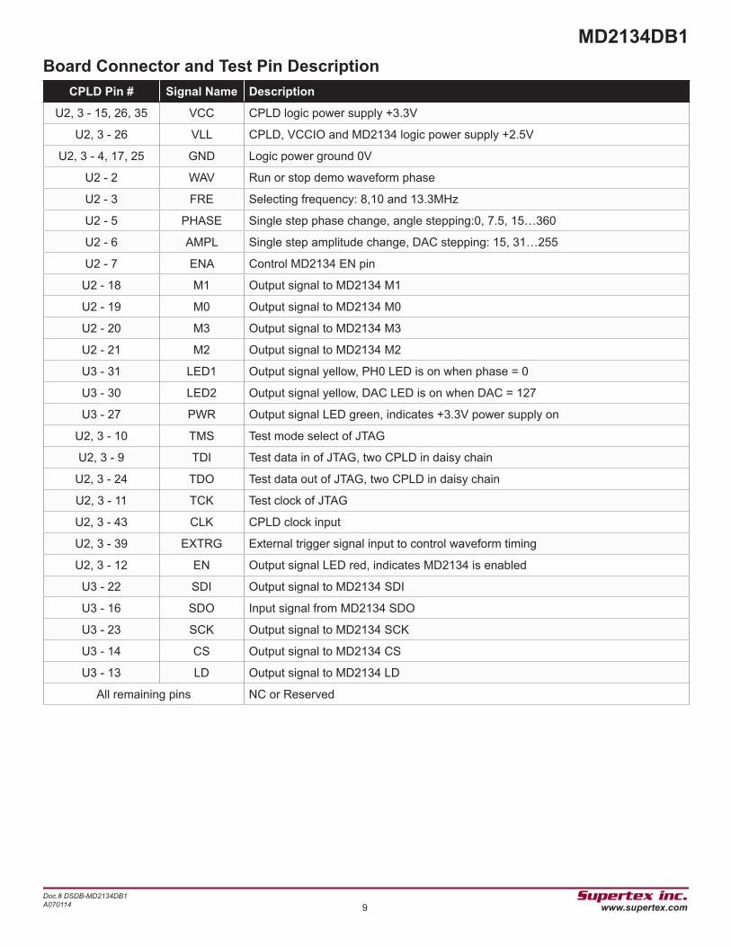
CPLD Pin # Signal Name Description
U2, 3 - 15, 26, 35 VCC CPLD logic power supply +3.3V
U2, 3 - 26 VLL CPLD, VCCIO and MD2134 logic power supply +2.5V
U2, 3 - 4, 17, 25 GND Logic power ground 0V
U2 - 2 WAV Run or stop demo waveform phase
U2 - 3 FRE Selecting frequency: 8,10 and 13.3MHz
U2 - 5 PHASE Single step phase change, angle stepping:0, 7.5, 15…360
U2 - 6 AMPL Single step amplitude change, DAC stepping: 15, 31…255
U2 - 7 ENA Control MD2134 EN pin
U2 - 18 M1 Output signal to MD2134 M1
U2 - 19 M0 Output signal to MD2134 M0
U2 - 20 M3 Output signal to MD2134 M3
U2 - 21 M2 Output signal to MD2134 M2
U3 - 31 LED1 Output signal yellow, PH0 LED is on when phase = 0
U3 - 30 LED2 Output signal yellow, DAC LED is on when DAC = 127
U3 - 27 PWR Output signal LED green, indicates +3.3V power supply on
U2, 3 - 10 TMS Test mode select of JTAG
U2, 3 - 9 TDI Test data in of JTAG, two CPLD in daisy chain
U2, 3 - 24 TDO Test data out of JTAG, two CPLD in daisy chain
U2, 3 - 11 TCK Test clock of JTAG
U2, 3 - 43 CLK CPLD clock input
U2, 3 - 39 EXTRG External trigger signal input to control waveform timing
U2, 3 - 12 EN Output signal LED red, indicates MD2134 is enabled
U3 - 22 SDI Output signal to MD2134 SDI
U3 - 16 SDO Input signal from MD2134 SDO
U3 - 23 SCK Output signal to MD2134 SCK
U3 - 14 CS Output signal to MD2134 CS
U3 - 13 LD Output signal to MD2134 LD
All remaining pins NC or Reserved
Board Connector and Test Pin Description

10
MD2134DB1
Supertex inc. www.supertex.com
Doc.# DSDB-MD2134DB1A070114
Voltage Supply Power-Up SequenceStep Signal Name Description
1 VDD +5.0, MD2134 positive supply voltages2 VCC +3.3V, MOSFET gate biasing and CPLD control logic supply voltage3 VPP +70V to 100V, the high voltage supply
4 ENLogic Active Enable logic control, active-high signal to MD2134
Voltage Supply Power-Down Sequence
1 ENLogic Active Disable logic control, active-high signal to MD2134
2 VPP +70V to 100V, the high voltage supply, off3 VDD +5.0V, MD2134 positive supply voltages with all input signals LOW, off4 VCC +3.3, CPLD control logic supply voltage with EN = 0, off
JTAG Connector
Pin #
Signal Name Description
J6-1 TMS Test Mode Select of CPLD.J6-2 TDI Test Data In of CPLD.J6-3 TDO Test Data Out of CPLD.J6-4 TCK Test Clock of CPLD.J6-5 GND Logic power supply ground 0V for programming only.J6-6 VCC Logic power supply +3.3V for programming only.
Signal and Jumper
Pin #
Signal Name Description
J1 EXCLK External clock input when on-board oscillator is disabled, or output of the clock when it is enabled.
J2 OSC_EN Jumper for on-board oscillator, short = disabled, open = enabled.J3 EXTRG External trigger signal input.J4 Load JP Jumper for on-board RC load to MD2134DB1 high voltage output and XDCR connector.
J5 XDCR MD2134DB1 waveform output, for SMA-cable to oscilloscope, high voltage! 0 to +/-350VP-P max.
Power Supply ConnectorJ7-1 VCC +3.3V, MOSFET gate biasing and CPLD supply voltage with current limit from 120 to
150mA.J7-2 GND Ground reference, 0V.J7-3 VDD +5.0V MD2134 positive supply voltages with current limit to 50mAJ7-4 GND Ground reference, 0V.J7-5 VPP +70 to100V, the high voltage supply with current limit to 30mA.
Supertex inc. does not recommend the use of its products in life support applications, and will not knowingly sell them for use in such applications unless it receivesan adequate “product liability indemnification insurance agreement.” Supertex inc. does not assume responsibility for use of devices described, and limits its liabilityto the replacement of the devices determined defective due to workmanship. No responsibility is assumed for possible omissions and inaccuracies. Circuitry andspecifications are subject to change without notice. For the latest product specifications refer to the Supertex inc. (website: http//www.supertex.com)
©2014 Supertex inc. All rights reserved. Unauthorized use or reproduction is prohibited. Supertex inc.1235 Bordeaux Drive, Sunnyvale, CA 94089
Tel: 408-222-8888www.supertex.com11
MD2134DB1
Doc.# DSDB-MD2134DB1A070114
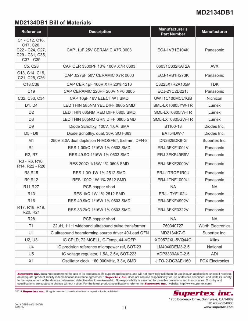
MD2134DB1 Bill of MaterialsReference Description Manufacturer’s
Part Number Manufacturer
C1 - C12, C16, C17, C20,
C22 - C24, C27, C29 - C31, C35,
C37 - C39
CAP .1µF 25V CERAMIC X7R 0603 ECJ-1VB1E104K Panasonic
C5, C28 CAP CER 3300PF 10% 100V X7R 0603 06031C332KAT2A AVXC13, C14, C15, C21, C25, C26 CAP .027µF 50V CERAMIC X7R 0603 ECJ-1VB1H273K Panasonic
C18,C36 CAP CER 1µF 100V X7R 20% 1210 C3225X7R2A105M TDK
C19 CAP CERAMIC 220PF 200V NP0 0805 ECJ-2YC2D221J Panasonic
C32, C33, C34 CAP 10µF 16V ELECT WT SMD UWT1C100MCL1GB Nichicon
D1, D4 LED THIN 585NM YEL DIFF 0805 SMD SML-LXT0805YW-TR Lumex
D2 LED THIN 635NM RED DIFF 0805 SMD SML-LXT0805IW-TR Lumex
D3 LED THIN 565NM GRN DIFF 0805 SMD SML-LXT0805GW-TR Lumex
D9 Diode Schottky, 100V, 1.0A, SMA B1100-13 Diodes Inc.
D5 - D8 Diode Schottky, dual, 30V, SOT-363 BAT54DW-7 Diodes Inc.
M1 250V 3.0A dual depletion N-MOSFET, 5x5mm, DFN-8 DN2625DK6-G Supertex Inc.
R1 RES 1.00kΩ 1/16W 1% 0603 SMD ERJ-3EKF1001V Panasonic
R2, R7 RES 49.9Ω 1/16W 1% 0603 SMD ERJ-3EKF49R9V PanasonicR3 - R6, R10,
R14, R22 - R26 RES 200Ω 1/16W 1% 0603 SMD ERJ-3EKF2000V Panasonic
R8,R15 RES 1.0Ω 1W 1% 2512 SMD ERJ-1TRQF1R0U Panasonic
R9,R12 RES 100Ω 1W 1% 2512 SMD ERJ-1TNF1000U Panasonic
R11,R27 PCB copper short NA NA
R13 RES 1kΩ 1W 1% 2512 SMD ERJ-1TYF102U Panasonic
R16 RES 49.9kΩ 1/16W 1% 0603 SMD ERJ-3EKF4992V PanasonicR17, R18, R19,
R20, R21 RES 33.2kΩ 1/16W 1% 0603 SMD ERJ-3EKF3322V Panasonic
R28 PCB copper short NA NA
T1 22µH, 1:1:1 wideband ultrasound pulse transformer 750340727 Würth Electronics
U1 IC ultrasound beamforming source driver 40-Lead QFN MD2134K7-G Supertex Inc.
U2, U3 IC CPLD, 72 MCELL, C-Temp, 44-VQFP XC9572XL-5VQ44C Xilinx
U4 IC precision reference micropower ref, SOT-23 LM4040DEM3-2.5 National
U5 IC voltage regulator, 1.5A, 2.5V, SOT-223 ADP3339AKC-2.5 ADI
X1 Oscillator clock, 160.000MHz, 3.3V, SMD JITO-2-DC3AE-160 FOX Electronics