supplementary figures - nature · supplementary figures ... transition from on to off state...
TRANSCRIPT

Supplementary Figures
Supplementary Figure S1 - Steady state emfs for the OFF state and the RESET transition from ON to OFF state corresponding to a dissolution of the filament
The dissolution is induced by three different factors: VGT, Vd, and also chemical reactions of dissolution within the electrolyte matrix30. The contribution of VGT in accordance to equation (6) is presented here. We programmed three different ON states in a Ag/GeS2.2/Pt system, characterized by three different resistances of 600 Ω, 1500 Ω and 3500 Ω, by setting two different current compliances of 100 µA, 10 µA and 1 µA, respectively. Please note that the devices we used for this experiment were deliberately not equipped with a thin oxide barrier in the electrolyte, so that the ON states were more unstable than in usual devices. In devices targeting memory applications such diffusion barriers are typically introduced to prevent a fast chemical dissolution of Ag into the glassy chalcogenides matrix and to limit the ON current densities. It is shown that all emfs in the ON state exhibit initially a short circuit resistance. The emf value (and the ON resistance) of the cell programmed at 100 µA remains constant within a long period of time indicating that the metallic filament was stable. For the cells programmed at current compliances of 10 µA and 1µA after a limited period of time a sharp increase of the emf was observed. This increase obviously corresponds to dissolution of the nanosized filament. In accordance to equation (6) the voltage is of a positive polarity. However, the impact of VGT cannot be separated by the impact of the diffusion emf i.e., Vd (which is also of positive polarity). The voltage equilibrates at values typical for the OFF state within 60 seconds. The subsequently measured high resistances confirm that the cells indeed underwent a RESET to OFF state. Similar behavior was also observed for WO3-x and GeSe2.3 based cells.

ν = 180 mV/s Ag/SiO2/Pt
A
B
C
D
E
F
G
0 0.25
Applied Voltage (V)
0.5 1 1.25 1.50.75-0.25-0.5
0
0.25
0.5
0.75
1
1.25
-0.25
-0.5
Cu
rren
t (µ
A)
0 250 500 7500
20
40
60
t (s)
Vce
ll (mV
)
A G V
I/V sweep stop Vcell
(t)
0 1 1.5-0.5-1-1.5
0
5
10
15
20
-5
-10
-15
-20
Applied Voltage (V)
Cu
rren
t (n
A)
cion = 1.4·10-4 M cm-3
Vce
ll (mV
)
0 200 400 6000
50
100
150
t (s)
A C V
I/V sweep stop Vcell
(t)
AB
C
initial sweep
Ag/SiO2/Pt
ν = 180 mV/s
(after switching and RESET)
a. b.
Supplementary Figure S2 – Current voltage characteristics for oxidation of Ag and reduction of Ag+ ions during device operation of a Ag/SiO2/Pt based ECM cell
The transient emf measurements correspond to Fig. 2b,c (a) Resistive Switching of a previously formed Ag/SiO2/Pt cell. For readability the switching curve is labeled by (A) to (G). Initially, the cell was SET into the ON state (A) to (D) and subsequently RESET into the OFF state (E) to (G). After RESET the I/V-sweep was stopped and the emf was immediately measured (red dotted line). (b) Cyclic voltammetry of a similar Ag/SiO2/Pt cell as used for resistive switching. Without forming40 and by limitation of the voltage amplitude (-1.5 V ≤ V ≤ 1.5 V) the Ag+/Ag redox-process can be observed41. The ion concentration cion can be adjusted by the sweep rate during oxidation and V > 0 (A) to (C).25 The emf as a function of the ion concentration was subsequently measured. Details on cyclic voltammetry can be found in38.

subsequent reduction cycles
1st RESET and reduction
initial curve
n cy
cles
ICC
-0.5 0 0.5 1
Applied Voltage (V)
1.5-1
Cu
rren
t (n
A)
0
2
4
6
-2
-4
ACell
= 5·10-4 cm2
ν = 420 mV/s
t
V
...n cycles
Ag/SiO2/Pt
Supplementary Figure S3 – Resistive Switching of a Ag/SiO2/Pt cell using a current compliance ICC = 5 nA
The cell was initially SET and RESET afterwards. After the first RESET subsequent current/voltage sweeps were performed in the negative voltage regime. The current clearly decreases by further cycling which is contributed to further reduction of previously oxidized silver ions. This behavior cannot be attributed to a trivial polarization effect. The non zero-crossing behavior is clearly demonstrated.
Here we show the situation when the cell was first SET and then RESET. The performed continuous subsequent cathodic cycles showed that the current further decreases with each cycle. This behavior clearly confirms that the measured non-pinched characteristics are due to the emf and not due to dielectric capacitance effects. Furthermore, the measured currents at a given potential value are linearly dependent on the sweep rate in the case of dielectric capacitive effects and proportional to a square root of the sweep rate in the case of Faraday currents, respectively. In our previous papers41, 25 we demonstrated that in Cu/SiO2/Pt systems the condition of a linear relation I vs. V1/2 is fulfilled. The observed Faraday peaks in the cyclic voltammogram also unequivocally proved that the currents are due to electrochemical reactions25.
d = 150 µm
d = 100 µmd = 250 µm
0.3
0.25
0.2
0.15
0.1
0.05
00 25 50 75 100 125 150
t (s)
J (µ
A c
m−
2)
Ag+
V = 0A
OH−
Ag/SiO2/Pt
Cu
rren
t (p
A)
05
0 1 2 3 4 5A
cell · 10-4 (cm2)
d = 100 µm
d = 150 µm
d = 250 µm
1015202530
t = 150 s
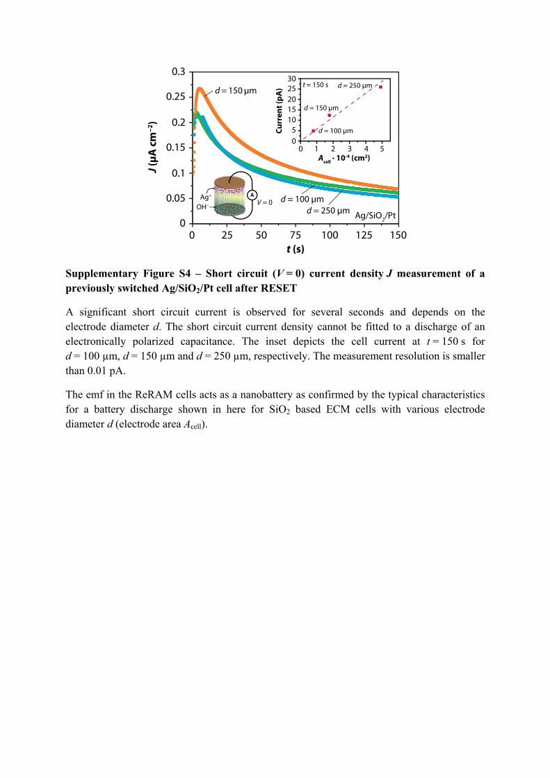
Supplementary Figure S4 – Short circuit (V = 0) current density J measurement of a previously switched Ag/SiO2/Pt cell after RESET
A significant short circuit current is observed for several seconds and depends on the electrode diameter d. The short circuit current density cannot be fitted to a discharge of an electronically polarized capacitance. The inset depicts the cell current at t = 150 s for d = 100 µm, d = 150 µm and d = 250 µm, respectively. The measurement resolution is smaller than 0.01 pA.
The emf in the ReRAM cells acts as a nanobattery as confirmed by the typical characteristics for a battery discharge shown in here for SiO2 based ECM cells with various electrode diameter d (electrode area Acell).

Supplementary Figure S5 – Sketch of the resistance components which make up the resistance of a VCM cell
In parallel to the (low) resistance of the filament, there is the resistance of the unformed, pristine film. The OFF and ON state are controlled by a higher or lower resistance of the “disc” at the end of the filament close the active electrode (left), while the stub (“plug”) of the filament remains unchanged in first approximation (reproduced from 42).
For pristine cells, properties such as the leakage current are area proportional within the first approximation. However, after electroforming this is not true anymore for filamentary ReRAM types. The ON state is determined by a metallic filament for ECM cells and a highly electronic-ionic conducting filament for VCM cells, leading to RON values independent of the area. Also in the OFF state, there is a fast ion transport channel along the original filament for ECM cells (this is the reason for the much lower SET voltage compared to the forming voltage). In the OFF state of VCM cells, most of the highly electronic-ionic conducting filament remains (this stub of the filament is called “plug”). The filament is just disrupted by a thin oxidized and, hence, more insulating barrier (“disc”) close to the active electrode.42 For this reason, downscaling from micrometer sized cells to nanometer sized cells will lead to an increase in the dominance of the conductance of the filament compared to the rest of the area.

0 20 40 60 80 100 1200
50
100
150
200
250
300
t (s)
Vce
ll (µV
)
TiN/TiO2/Ti
after switching and RESET
Supplementary Figure S6 – Transient cell voltage measurement of a Ti/TiO2/TiN nanocrossbar cell
The measurement of the nanocrossbar cell (≈ 55 nm · 55 nm) has been immediately performed after switching and RESET. The 10 nm thick TiO2 layer has been fabricated by reactive sputtering. A Pt layer has been additionally deposited on the Ti top electrode in order to prevent chemical oxidation of Ti in air. Please note that this is a preliminary result which awaits confirmation by extended statistical studies. The result indicates that indeed Vcell can be detected for nanoscale ReRAM cells.
In general, if high-temperature bulk diffusion data are used to estimate the switching kinetics of ReRAMs, great care must be exercised. For instance, the Ag cation diffusion coefficients in SiO2 43 measured at temperatures between 525 K and 875 K and extrapolated to slabs of 10 nm thickness at 300 K lead to a diffusion coefficient of 2.10-23 cm2/s (electrical mobility of ~ 4.10-22 cm2/Vs). Hence, switching of a ECM-type Ag/SiO2/Pt cell (as used in our study) at e.g. 1 V would need over 75 years (!) to switch. In VCM cells similar calculations44 lead to switching times (at V = 1 V and film thickness of 10 nm) of more than 30 hours including a field acceleration component. In reality, however, we (and many other groups working in this field) can switch such cells in < 10 ns. Translated into Ri (assuming the same concentration of mobile charges), there is > 10 orders of magnitude difference between the extrapolated bulk values and the experimental thin film switching times. The reason for the discrepancy is not known yet. It may be speculated that the thin films deposited by sputtering, ALD, evaporation etc., typically at much lower temperature than bulk sintering or melting, show a nanoporosity which strongly enhances the ion mobility. Furthermore, it is conceivable that different diffusion paths (such as extended defects) start to dominate at lower temperatures. A significant acceleration (up to orders of magnitude) will arise for the field acceleration of the ion mobility due to the high fields (> 1 MV/cm) in the disc in front of the active electrode in assumed to be the range from 3 to 5 nm, responsible of the actual modification of the electrostatic barrier. In principle, different diffusion regimes (e.g. due to approaching nano-dimensions 45, 46 and when the film thickness is comparable to the space charge layer thickness 47, 48) are well known in material science for many years. In VCM cells, a disc in front of the active electrode is smaller in thickness than typically space charge layers 17, 2.

0
t (h)
1 2 3 4 5 6200
250
300
350
400
450
500
Vce
ll (mV
)
Cu/SiO2/Pt
ν = 43 mV/s
0 50 100 150 200 250 300
t (s)
0
0.2
0.4
0.6
0.8
1
Vce
ll (V)
Cell #1 Cell #2 Cell #3
Pt/SrTiO3/TiRasdep ≈ 10 GΩ
a. b.
Supplementary Figure S7 – Transient emf measurements for unformed cells
Here steady state cell voltages are shown for as-deposited cells after anodic oxidation without forming and resistive switching for (a) Pt/SrTiO3/Ti and (b) Cu/SiO2/Pt.
In the as-deposited state the ReRAM cells based on the valence change mechanism (VCM) show a cell voltage which is comparable to that of the ECM cells. Thus, both unformed VCM and ECM systems show cell voltages in the order of some hundreds of millivolts.
Cell #1
0 50 100 150 200 250 300
t (s)
1.45
1.5
1.55
1.6
1.65
1.7
1.75
Vce
ll (mV
)
Cell #2 Cell #3 Cell #4 Cell #5
Pt/SrTiO3/TiROFF ≈ 1 MΩ
a. b.
0 10 20 30 40 50 60
0
50
100
150
200
250
300
350
t (s)
Vce
ll (µV
)
OFF state cell #1
OFF state cell #2
ON state cell #1ON state cell #2
Pt/Ta2O
5/Ta
ROFF ≈ 100 MΩ
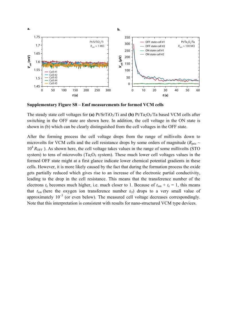
Supplementary Figure S8 – Emf measurements for formed VCM cells
The steady state cell voltages for (a) Pt/SrTiO3/Ti and (b) Pt/Ta2O5/Ta based VCM cells after switching in the OFF state are shown here. In addition, the cell voltage in the ON state is shown in (b) which can be clearly distinguished from the cell voltages in the OFF state.
After the forming process the cell voltage drops from the range of millivolts down to microvolts for VCM cells and the cell resistance drops by some orders of magnitude (Rpris ~ 104 ROFF ). As shown here, the cell voltage takes values in the range of some millivolts (STO system) to tens of microvolts (Ta2O5 system). These much lower cell voltages values in the formed OFF state might at a first glance indicate lower chemical potential gradients in these cells. However, it is more likely caused by the fact that during the formation process the oxide gets partially reduced which gives rise to an increase of the electronic partial conductivity, leading to the drop in the cell resistance. This means that the transference number of the electrons te becomes much higher, i.e. much closer to 1. Because of tion + te = 1, this means that tion (here the oxygen ion transference number tO) drops to a very small value of approximately 10–3 (or even below). The measured cell voltage decreases correspondingly. Note that this interpretation is consistent with results for nano-structured VCM type devices.

0 0.5 1 1.5-0.5-1
-0.5
0
0.5
1
Cu
rren
t (µ
A)
Applied Voltage (V)
Applied Voltage (V)0 0.5-0.5
0
2
4
-4
-2
Cu
rren
t (n
A)
ν = 400 mV/s
Ag/SiO2/Pt
Zoom
ACell
= 2·10-4 cm2
A
B
C
D
AB
C
D
Supplementary Figure S9 – Non zero-crossing I/V-curve of Ag/SiO2/Pt cells
The resistive switching characteristics of Ag/SiO2/Pt cells are comparable to the Cu based cell I/V curves depicted in Fig. 4b. The red curve is highlighted while statistical variation of subsequent cycles is depicted in grey color. For readability the current is labeled by (A) to (D). The non zero-crossing characteristic after RESET is clearly observed in the inset.

Applied Voltage (V)
0
0.5
1
-0.5
-10-0.5-1
Cu
rren
t (m
A)
ACell
= 1·10-4 cm2
Ti/SrTiO3/Pt
B
C
Zoom
A
-1.5
-1
-0.5
0
0.5
0 5-5Applied Voltage (mV)
Cu
rren
t (µ
A)
10-10
1
A
B
C
Supplementary Figure S10 – Non zero-crossing I/V-curve of Ti/SrTiO3/Pt cells
The red curve is highlighted while statistical variation of subsequent cycles is depicted in grey color. For readability the current is labeled by (A) to (D). The non zero-crossing characteristic after RESET is clearly observed in the inset.
Similar to ECM cells the cyclic voltammetry with VCM cells is characterized by non zero-crossing characteristics with currents of up to 0.5 µA for the Ti/SrTiO3/Pt system as shown here.
We should note that in case of VCM cells filaments composed of a partially reduced phase can also facilitate a non-zero cell voltage in the ON state. As long as some minor part of the total conductivity remains ionic even the ON state can experience the cell voltage. This can be observed in the I-V cruve here where an offset is also present for the ON state (and as expected smaller compared to the OFF state).

Supplementary Figure S11 – Emf and resistive switching simulation results
(a) First (marked by red color) and second cycle (marked by green color) of the extended memristive device simulation. (b) Zoom showing the non zero-crossing characteristic. The increase of the concentration cion leads to an increase of emf, hence the y-axis intercept varies from cycle to cycle. (c) Vemf (from (a)) as function of time. Note, Vemf cannot be experimentally determined in the ON state (dashed line) due to the electronic short circuit by the filament. (d) emf versus ion concentration.

VS (µ
V)
-10
0
10
20
30
40
50
0 100 200 300 400
t (s)
Vtot
= 5 V
4 V
3 V
2 V
1 V0.5 V
0
Vtot
(V)5 10−5−10
10−7
10−6
10−5
10−4
calculatedmeasurement
VS (
V)
R1
RS
Vtot
VS
a. b.
Supplementary Figure S12 – Measurement resolution
The voltage measurement accuracy can be tested by measuring the voltage drop VS across a shunt resistor RS by variation of the applied voltage Vtot (RS = 10 Ω and R1 = 10 MΩ). (a) Small voltages even below 10 µV can be clearly measured and fit to the calculated voltage drop. (b) Voltage pulses with variation of the pulse amplitude Vtot reveal a sufficient SNR (signal to noise ratio). All measurements of this study were performed in ultra low noise, dark and RF shielded measurement systems to prevent radio frequency interference (RFI) and electromagnetic interference (EMI) in accordance to ref. 49. The triaxial measurement setup makes it possible to measure currents well below the pA range and significantly reduces the effective cable capacitance.50 The measurement resolution has been checked to be within the device specification (Keithley 6430 Subfemto Remote SourceMeter, Keithley 617 Electrometer and Keithley 2636A SourceMeter). The current measurement resolution for short circuit measurements (compare Fig. 2d) is about 0.01 pA. Three additional control experiments were conducted to exclude RFI or EMI effects as the origin of our emf voltage: (1) we transferred the measurement system into a RF shielded room and we repeated selected experiments. The results did not change within the measuring accuracy. (2) We tested a symmetric Pt/GeSex/Pt cell which should not show any significant cell voltage. In fact, the open cell voltage was in the noise level, i.e. no emf voltage has been detected. (3) Furthermore, we determined the voltage resolution limit of our system.
The peak-to-peak noise level shown here is approx. 7 µV, whereas the rms noise signal is 1 µV. As a consequence, voltages below 10 µV can be clearly measured. Since the voltage divider was placed in the same measurement system, the voltage stimulation steps and their response provide an additional proof that RFI or EMI effects can be excluded. A thermoelectric effect as the origin of our emf voltage can be excluded because of the orders of magnitude different time constants. We measured the transient (steady-state open-cell) voltages from several minutes up to hours and even for days (e.g. see Supplementary Figure S7) while any temperature differences caused by prior switching vanish within nanoseconds to microseconds due to the small volume of the switching region. All emf measurements were performed at room temperature and after temperature gradients were equilibrated. Please note that emf voltages were measured in the OFF (or unformed) state using high impedance source meters.

Supplementary Tables
System Rtot Ri Re Ri/Rtot Cu/SiO2/Pt 4 GΩ 13 GΩ a 5.8 GΩ 3.3 c Ag/SiO2/Pt 0.4 GΩ 0.9 GΩ a 0.7 GΩ 2.5 c,d Ag/GeS2.2/Pt 3 kΩ b 3.4 kΩ 27 kΩ 1.13 c,e Ag/GeSe2.3/Pt 1 kΩ b 1.3 kΩ 4.5 kΩ 1.3 c,e Ag/AgI/Pt 0.2 GΩ 0.3 GΩ a 0.6 GΩ 1.3 e Cu/WOx/Pt 0.4 GΩ b 1.1 GΩ 0.6 GΩ 2.75 c Pt/SrTiO3/Ti 1 MΩ 1 GΩ a ~ 1 MΩ ~103 f Pt/Ta2O5/Ta 10 kΩ 10 MΩ a ~ 10 kΩ ~103 f
a Short Circuit measurement (calculated by cell voltage and short circuit current) b Impedance spectroscopy (using a PARSTAT 2273, input impedance 1013 Ω, ac-amplitude 20 mV, frequency range 2 MHz to 1 Hz) c Hebb-Wagner measurement (refs 51, 52) d emf slope (see Fig. 2c and eq. (11)) e emf method in Ag/Electrolyte/C(I2) cell f Maximum transference number estimation based on the ratio of charge during switching and maximum amount of O2- ions in the cell which can be oxidized.
Supplementary Table S1 – Cell resistance values
The resistance values for the total (Rtot), the ion (Ri) the electronic (Re) resistances, respectively and the ratio Ri/Rtot are summarized here. The methods used for determining the values are summarized in the trailer of the table. Please note that the electronic resistance Re for ECM cells in the OFF state is mainly determined by the leakage current Rleak.
We calculated these values on the basis of V = Vcell and Imax (at V = 0) or from the total resistance measured by impedance spectroscopy and the transference numbers tion = (Ri/Rtot)-1. Because Ri depends on the surface area of the electrodes we provided the value Ri/Rtot which is area independent. The Ri/Rtot value is included in Fig. 4a.
The value of Ri (and Rtot) and also the ratio Ri/Rtot usually depends strongly on the chemical composition, on the amount of the dopant (e.g. Ag), electrolyte thickness, temperature, and gas atmosphere. Thus, the values we provide in the table are valid strictly for the corresponding system and may significantly vary if some of the parameters (e.g. amount of Ag ion doping) are changed.

System Measurement Number of experiments
Ag/SiO2 (30 nm … 50 nm)/Pt;
d = 100 µm, 150 µm, 250 µm
Resistive Switching using I/V sweeps, SET/RESET experiments (examples shown or used in Fig. 2b, 2d, Supplementary Figure S2a, S3, S4, S9)
320
Ag/SiO2 (50 nm)/Pt; d = 100 µm, 150 µm, 250 µm
Short circuit current (V = 0) after RESET (examples shown in Fig. 2d, Supplementary Figure S4)
35
Ag/SiO2 (50 nm)/Pt; d = 100 µm, 150 µm, 250 µm
Cyclic Voltammetry (examples shown or used in Fig. 2b, 2c, Supplementary Figure S2b)
36
Ag/SiO2 (50 nm)/Pt; d = 100 µm, 150 µm, 250 µm
Emf measurements (examples shown or used in Fig. 2b, 2c, 4a, Supplementary Figure S2)
29
Cu/SiO2 (30 nm)/Pt; d = 100 µm
Resistive Switching using I/V sweeps, SET/RESET experiments (example shown in Fig. 4b)
38
Cu/SiO2 (30 nm)/Pt; d = 100 µm
Emf measurements and Cyclic Voltammetry (examples shown or used in Fig. 4a, Supplementary Figure S2b, S7b, )
106
Ag/AgI (30 nm … 50 nm)/Pt; ACell = 3 µm x 3 µm (crossbar)
Emf measurements and Resistive Switching (example used in Fig. 4a)
49
TiN/TiO2 (10 nm)/Ti; ACell = 55 nm x 55 nm
Emf measurements and Resistive Switching (example used in Fig. Supplementary Figure S6)
1
Pt/SrTiO3 (10 nm)/Ti; ACell = 10-4 cm2
Resistive Switching (examples used or shown in Fig. 4a,Supplementary Figure S7a, S8a, S10)
75
Pt/SrTiO3 (10 nm)/Ti; ACell = 10-4 cm2
Emf measurements (example used in Fig. 4a, Supplementary Figure S7a, S8a )
70
Pt/Ta2O5 (10 nm)/Ti; ACell = 10-4 cm2
Resistive Switching (examples used or shown in Fig. 4a, Supplementary Figure S8b )
87
Pt/Ta2O5 (10 nm)/Ti; ACell = 10-4 cm2
Emf measurements (examples used or shown in Fig. 4a, Supplementary Figure S8b )
80
Cu/WO3 (30 nm)/Pt; d = 50 µm
Emf measurements and Resistive Switching (used in Fig. 4a and , Supplementary Figure S1)
15
Ag/GeS2.2 (40 nm … 70 nm)/Pt; d = 100 µm
Emf measurements and Resistive Switching (used in Fig. 4a and Supplementary Figure S1)
30

Ag/GeSe2.3 (40 nm … 70 nm)/Pt; d = 100 µm
Emf measurements and Resistive Switching (used in Fig. 4a, and Supplementary Figure S1)
24
Ag/GeSe2.3 (40 nm … 70 nm)/Pt; d = 100 µm
Optical analysis of dendrites (used in Fig. 3)
4
Supplementary Table S2 – Measurement summary
Summary of switching and emf experiments performed in the context of this study.
Supplementary Note 1
On the use of the term ‘Memristor’
The memristor was theoretically derived in 1971 by L. Chua as a non-linear circuit element correlating flux-linkage φ and charge q 8. From an axiomatic point of view, this device was considered the fourth element besides non-linear resistors, non-linear inductors and non-linear capacitors. The hypothetical device offers a one-to-one mapping of φ and q and can be either described as a voltage or current controlled device.
Voltage controlled:
( )φ= ⋅I G V
φ =V (S1)
Current controlled:
( )= ⋅V R q I
=q I (S2)
In 1976 the memristor concept was generalized towards memristive systems by L. Chua and S. M. Kang to cover a wide range of real devices 9. Corresponding memristive elements are characterized by an I-V hysteresis loop pinched at the origin, which the authors call a zero-crossing property. A memristive element offers an arbitrary number of internal state-variables
[ ]1...= nx xx .
Voltage controlled:
( , )= ⋅I G x V V
( , )= f Vx x (S3)
Current controlled:
( , )= ⋅V R x I I
( , )= f Ix x (S4)
Several physical devices such as thermistors and discharge tubes were modeled as memristive elements.9 Moreover, a Hodgkin-Huxley neuron could be modeled as memristive element and an additional battery in series. Note that this modeling approach is not feasible for ReRAM cells where the controlling ionic battery path is in parallel to the controlled electronic resistance (see Supplementary Note S4).
In 2008 TiOx based VCM devices were identified as memristive elements by Strukov et al. 6. In 2011 L. Chua suggested to use the term ‘memristor’ for any ReRAM cell 23 and calling any memristive systems a ‘memristor’. Please note this ‘real’ memristor does not represent the

fourth element anymore and must not be confused with the (still hypothetical) ‘ideal’ memristor (definition from 1971 8). In the line of the redefinition ReRAM cells have been considered ‘memristors’.23 In our paper we show that the redefinition may be true for e.g. STT-MRAM devices, however, this is not applicable for ReRAM cells because of the inherent nanobattery which violates the I-V pinched zero-crossing properties. For this reason, we suggest an extension of the memristor theory as outlined in the main text.
Supplementary Note 2
Derivation of equation (10) on the basis of linear combination of equations (5) and (9)
The potential determining electrode reaction at the interface Ag/SiO2 (s'):
Ag+Ag
Ag
Ag Ag with e
ae K
a a+ −
−+ = (S5)
The potential determining electrode reaction at the interface Pt/SiO2 (s''):
12 2
2 2
2OH1
2 2 2 H O 2O H O
O H O 2 2OH with e
ae K
a a a−
−
− −+ + =⋅ ⋅ (S6)
Nernst potential contribution:
12
2 2
2 2s' s''0 Me OH
N 2Me s' O s'' H O s''
( ) ( )ln
2 ( ) ( ) ( )+ −⋅
= +⋅ ⋅
za akTV Ve a a a (S7)
Diffusion potential contribution ( +Me1z = + for Ag+ and 1z− = − for electrons and OH-):
+
s's'Me Me s'
ds'' s''s'' Me Me
s' s' s'Ag OHAg OH
s'' s'' s''Ag OH
( ) ( )ln ln ln( ) ( )
( ) ( ) ( )ln ln ln
( ) ( ) ( )
ii
i i
ee
e
t at akT kT tV d ae z e z a z a
a a akT kT kTt t te a e a e a
+ +
+
+ − −
+ − −
+ − −
−−
− −
⎛ ⎞= − = − −⎜ ⎟⎜ ⎟
⎝ ⎠
= − − −
∑ ∫
(S8)
In accordance to equations (S5) and (S6) one substitutes:
Ag ss'
s AgAg
( )( )
( )e
aa
a K−
+
′
′
= , 1 1 14 2 2
2 2 2
sOHs''
O s H O s H O
( )( )
( ) ( )e
aa
a a K−
−
′′
′′ ′′
=⋅ ⋅
and OH Ag
1et t t− − += − − .
In this way the term of electronic transference number is expressed as:
( )1 1 1
4 2 2
2 2 2Ag s O s H O s H Os'OH Ag
s'' s Ag sAg OH
( ) ( ) ( )( )ln 1 ln
( ) ( ) ( )e
ee
a a a Kat t t
a a K a−
− − +
− + −
′ ′′ ′′
′ ′′
⋅ ⋅= − − (S9)

Or equation (S8) reads:
( )1 1 1
4 2 2
2 2 2
s' s'Ag OHd Ag OH
s'' s''Ag OH
Ag s O s H O s H OOH Ag
s Ag sAg OH
( ) ( )ln ln
( ) ( )
( ) ( ) ( ) 1 ln
( ) ( )
a akT kTV t te a e a
a a a KkTt te a K a
+ −
+ −
+ −
− +
+ −
′ ′′ ′′
′ ′′
= − −
⋅ ⋅− − −
(S10)
The emf of the cell is determined by the sum of the both contributions:
emf N dV V V= + (S11)
Substituting equation (S7) and equation (S10) in equation (S11) and accounting for the canceling and constant terms in the logarithms one derives the equation:
0emf s' s'' 0 ion ionOH Me Me OH
0
. ln( ) ln( ) ln( )2V
kT kT kTV V const t a t a V t ae e e− + + −= + + + +∼ (S12)
The emf in accordance to eq. (S11) and respectively, eq. (S12) represents the general case of possible origins of the emf. In fact not all contributions must always be present. For example the diffusion potential contribution (eq. (S8)) can be minimized or even completely eliminated in case of charged species with a high mobility, i.e. fast relaxation. Nernst potential (eq. (S7)) can be eliminated by using the same electrode materials. However, a complete simultaneous elimination of non-equilibrium conditions for ReRAM devices of practically application is not possible. Thus, the emf is perpetually induced in these devices during the operation and/or reading cycles but it can relax with time. The relaxation time depends strongly on the particular system, the transport properties of the conducting solid and the thermodynamic conditions.
Supplementary Note 3
Emf and volatility of the OFF state
The nanobattery effect is observed mainly for the OFF state. There is self-discharge (i.e. current flow under open-circuit conditions) of the nanobattery over Ri and Re (Fig. 2a), where Re may be mainly determined by Rleak in the OFF state (Fig. 5). This self-discharge process typically shows at least two time constants where the first time constant is in the order of some hundred seconds (see e.g. Fig. 2c) and a second time constant is in the order of many thousand seconds. For the VCM-type cells we typically observe a faster self-discharge obviously due to the lower Re. In any case, the self-discharge of these ReRAMs will occur at times much shorter than 10 years (retention time requirement for non-volatile memories). However, the relaxation of the voltage does not lead to a loss of the logic state (which would mean that the cell changes from the initial OFF state into the ON state due to the self-discharge). Admittedly, the relaxation may lead to a certain drift of the OFF state resistance.

Of this reason it is important to account for the existence of the nanobattery effect in the ReRAM cells. For example, the OFF resistance of nanoscale TiOx based cells drifts from 100 MΩ to 1-100 GΩ within 3 weeks.27 Shifts in ROFF are also reported for ECM cells.28 These drift processes may easily be caused by an emf voltage and would then demonstrate the relevance to device retention issues.
Thus, it is important to acknowledge that an emf is not necessarily leading to volatility of the state.2
Supplementary Note 4
Simulation Details
Extended memristive modelling
Our extended memristive model contains three parallel current paths: The state-dependent electronic current path (filament), the state-independent electronic leakage current path (neglected for the simulation), and the ionic current path.
The resistance of the ionic current path (Ri) is a sum of the polarization resistances (Butler-Volmer equation) at both electrodes (anode Rp,a and cathode Rp,c) and the ionic resistance Rion of the electrolyte (materials property) given by: Ri(V) = Rp,a + Rp,c + Rion. Ri is the derivative dV/dI and can be influenced by each of the three components which all offer a highly nonlinear voltage dependence. The field acceleration of the ion mobility leads to pronounced decrease of Ri for high field (above approx. 1 MV/cm) and, hence, to a strong non-linearity of Ri(V). Thus, the Ri value depends on the materials system and the applied voltage and can be individually calculated for the particular conditions, i.e. kind of electrolyte, applied voltage, temperature etc. However, to ensure the feasibility of the ReRAM device operation Ri(V) must have a finite value.
The two-dimensional state variable x consists of the structural variable (tunnelling gap) x and the variable representing the ionic concentration cion:
ion[ , ]x c=x (S13)The state-dependent Ohm’s law of the extended memristive device reads:
( ) ( )el ion ion, ,I I V x I V c= +, (S14)
and the corresponding two-dimensional state equation reads in case of anodic oxidation (i.e. charge and filament growth):
( )( )( )
1 ion ion
ion min ion max2 ion ion
, with 0 f ,
with ,
K I V cx x dV
c c c cK I V c
⎡ ⎤⋅ ≤ ≤⎡ ⎤ ⎢ ⎥= = =⎢ ⎥ ≤ ≤⎢ ⎥⋅⎣ ⎦ ⎣ ⎦x x
.
(S15)
The sign of K1 and K2 are reversed for cathodic sweep (discharging, i.e. V < Vemf).
To calculate the electronic current path, we apply the following tunnelling equation53:

( ) filel 0 eff 02
fil0 eff 02
4, exp 22 2 2
4exp 22 2 2
eA eV x eVI V x mhx h
eA eV x eVmhx h
πϕ ϕπ
πϕ ϕπ
⎛ ⎞⎛ ⎞= − − −⎜ ⎟⎜ ⎟ ⎜ ⎟⎝ ⎠ ⎝ ⎠⎛ ⎞⎛ ⎞− + − +⎜ ⎟⎜ ⎟ ⎜ ⎟⎝ ⎠ ⎝ ⎠ .
(S16)
Here, Afil is the area of the filament (rfil = 1 nm), φ0= 3.6 eV is the barrier height, meff = m0 is the effective electron mass. The tunnelling equation accounts for the increasing electronic contribution shortly before switching to the ON state.32 For the ionic current we use a Butler-Volmer equation to describe the electron transfer reaction of ions at the electrode interfaces:
( ) ( )emf ionion ion 0, sinh
4V V c
I V c IkT e
⎛ ⎞−= ⋅ ⎜ ⎟
⎝ ⎠
(S17)
For the simulation the following parameters were used (Ag/SiO2/Pt cell): I0: exchange current (2 nA) α: charge transfer coefficient (0.5) z: charge number (1) T: temperature (300 K)
In equation (S15) and (S17), dynamic effects, in particular the impact of the sweep rate41, diffusion limitation25 and potential multi-step redox-reactions, are neglected to simplify the model. We assume identical interfaces (s' and s'').32
The emf depends on the ion concentration, thus
( ) ionemf ion 0
0ln
2kT cV c V
e c⎛ ⎞
= + ⎜ ⎟⎝ ⎠
(S18)
with V0 = 0.17 V (see main text) holds true.
Simulated I-V sweeps and influence of the dielectric capacitance
In Supplementary Figure S11 the currents for the different sweeps do not overlay. Since the ion concentration during the sweeps changes, the emf varies correspondingly. The reason for changing the ion concentration is that during the cathodic sweep not all ions generated due to oxidation are reduced. The oxidation sweep continues up to 0.5 V whereas the cathodic one only to –0.3 V. Thus some ions remained and caused the current shift.
The dielectric capacitance of the cells can be derived as follows:
0 rε ε=ACd
(S19)
Here, the relative permittivity is assumed as r 5.5ε = for SiO2 54, the area is A =π (50 µm)2
and the thickness is d = 50 nm. The corresponding capacitance for the Ag/SiO2/Pt cell is C = 7.6 pF. In the simulation, a sweep rate of 1 V/s leads to a dielectric charging current of about 8 pA which is negligible compared to the current of 0.8 nA (see Supplementary Figure S11).

We checked a serial battery added to a memristive element as an alternative approach beside the model depicted in Fig. 5. The simulations show, however, that both ON and OFF states result in offsets on the voltage axis by the Vemf. This is in clear contrast to our experimental findings showing a zero cell voltage for a short circuited (metallic) ON state and non-zero cell voltage for only the OFF state. Thus, a pure serial connection of a passive memristive element plus battery, as for example present in the Hodgkin–Huxley model31, is not sufficient for ReRAM modelling.
Supplementary References
40. Tsuruoka, T., Terabe, K., Hasegawa, T. & Aono, M. Forming and switching mechanisms of a cation-migration-based oxide resistive memory. Nanotechnology 21, 425205 (2010).
41. Tappertzhofen, S., Menzel, S., Valov, I. & Waser, R. Redox Processes in Silicon Dioxide Thin Films using Copper Microelectrodes. Appl. Phys. Lett. 99, 203103 (2011).
42. Waser, R., Menzel, S. & Bruchhaus, R. Redox-Based Resistive Switching Memories, in: Nanoelectronics and Information Technology (3rd edition, Wiley-VCH, 2012).
43. McBrayer, J. D., Swanson, R. M. & Sigmon, Y. W. Diffusion of metals in silicon dioxide. J. Electrochem. Soc. 133, 1242-6 (1986).
44. Noman, M., Jiang, W., Salvador, P. A., Skowronski, M. & Bain, J. A. Computational investigations into the operating window for memristive devices based on homogeneous ionic motion. Appl. Phys. A - Mater. Sci. Process. 102 (2011).
45. Kosacki, I., Rouleau, C. M., Becher, P. F., Bentley, J. & Lowndes, D. H. Nanoscale effects on the ionic conductivity in highly textured YSZ thin films. Solid State Ionics 176, 1319-1326 (2005).
46. Korte, C., Schichtel, N., Hesse, D. & Janek, J. Influence of interface structure on mass transport in phase boundaries between different ionic materials. Monatshefte für Chemie - Chemical Monthly 140, 1069-1080 (2009).
47. Maier, J. Nanoionics: ion transport and electrochemical storage in confined systems. Nat. Mater. 4, 805-815 (2005).
48. Maier, J. Thermodynamics of Nanosystems with a Special View to Charge Carriers. Adv. Mater. 21, 2571-2585 (2009).
49. Keithley, Low Level Measurements Handbook (Keithley Instruments Inc., 2004).
50. Keithley, Application Note 1671: Low Current Measurements (Keithley Instruments Inc., 2012).
51. Carl Wagner, Proc. 7th Meet. Int. Comm. On Electrochem. Thermodynam. Kinet. Butterworths, London (1957).

52. Hebb, M. H. Electrical Conductivity of Silver Sulfide. The Journal of Chemical Physics 20, 185-190 (1952).
53. Simmons, J. G. Generalized Formula for the Electric Tunnel Effect between Similar Electrodes Separated by a Thin Insulating Film. J. Appl. Phys. 34, 1793-1803 (1963).
54. Tappertzhofen, S. et al. Capacity based Nondestructive Readout for Complementary Resistive Switches. Nanotechnology 22, 395203 (2011).