supplementary information lc-art-05-2010-000013 revision
TRANSCRIPT
Supplementary Material (ESI) for Lab on a Chip This journal is © The Royal Society of Chemistry 2010
Supplementary Information Fabrication Process Flow
A more detailed process flow for the nDSab is detailed in Table S1, including the specific
process conditions, the equipment model designations and manufacturers, and the suppliers for
all materials. Figure S1 schematically depicts the 11 die positions scanned using atomic force
microscopy (AFM) to determine the nanotrench depth prior to anodically bonding the Pyrex cap.
Scanning electron micrographs of the cross section of the nDS is displayed in Figure S2. Table S1: The process flow for the 22nm anodically bonded nanochannels
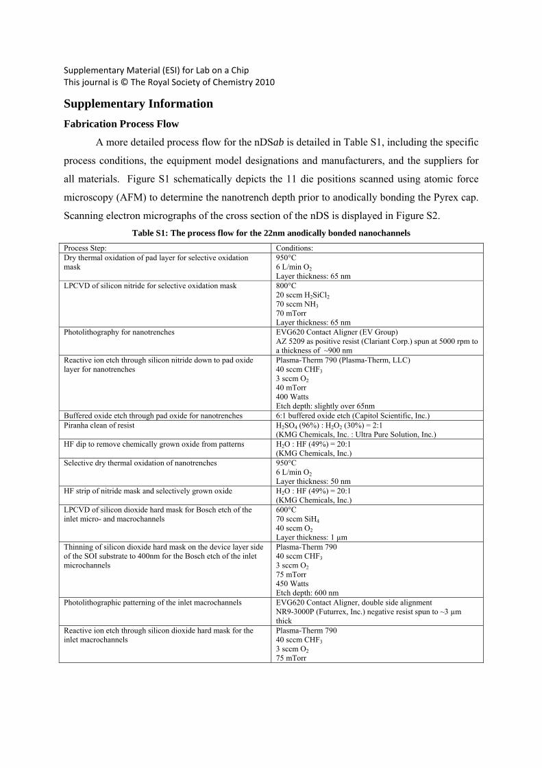
Process Step: Conditions: Dry thermal oxidation of pad layer for selective oxidation mask
950°C 6 L/min O2 Layer thickness: 65 nm
LPCVD of silicon nitride for selective oxidation mask 800°C 20 sccm H2SiCl2 70 sccm NH3 70 mTorr Layer thickness: 65 nm
Photolithography for nanotrenches EVG620 Contact Aligner (EV Group) AZ 5209 as positive resist (Clariant Corp.) spun at 5000 rpm to a thickness of ~900 nm
Reactive ion etch through silicon nitride down to pad oxide layer for nanotrenches
Plasma-Therm 790 (Plasma-Therm, LLC) 40 sccm CHF3 3 sccm O2 40 mTorr 400 Watts Etch depth: slightly over 65nm
Buffered oxide etch through pad oxide for nanotrenches 6:1 buffered oxide etch (Capitol Scientific, Inc.) Piranha clean of resist H2SO4 (96%) : H2O2 (30%) = 2:1
(KMG Chemicals, Inc. : Ultra Pure Solution, Inc.) HF dip to remove chemically grown oxide from patterns H2O : HF (49%) = 20:1
(KMG Chemicals, Inc.) Selective dry thermal oxidation of nanotrenches 950°C
6 L/min O2 Layer thickness: 50 nm
HF strip of nitride mask and selectively grown oxide H2O : HF (49%) = 20:1 (KMG Chemicals, Inc.)
LPCVD of silicon dioxide hard mask for Bosch etch of the inlet micro- and macrochannels
600°C 70 sccm SiH4 40 sccm O2 Layer thickness: 1 µm
Thinning of silicon dioxide hard mask on the device layer side of the SOI substrate to 400nm for the Bosch etch of the inlet microchannels
Plasma-Therm 790 40 sccm CHF3 3 sccm O2 75 mTorr 450 Watts Etch depth: 600 nm
Photolithographic patterning of the inlet macrochannels EVG620 Contact Aligner, double side alignment NR9-3000P (Futurrex, Inc.) negative resist spun to ~3 µm thick
Reactive ion etch through silicon dioxide hard mask for the inlet macrochannels
Plasma-Therm 790 40 sccm CHF3 3 sccm O2 75 mTorr
Supplementary Material (ESI) for Lab on a Chip This journal is © The Royal Society of Chemistry 2010
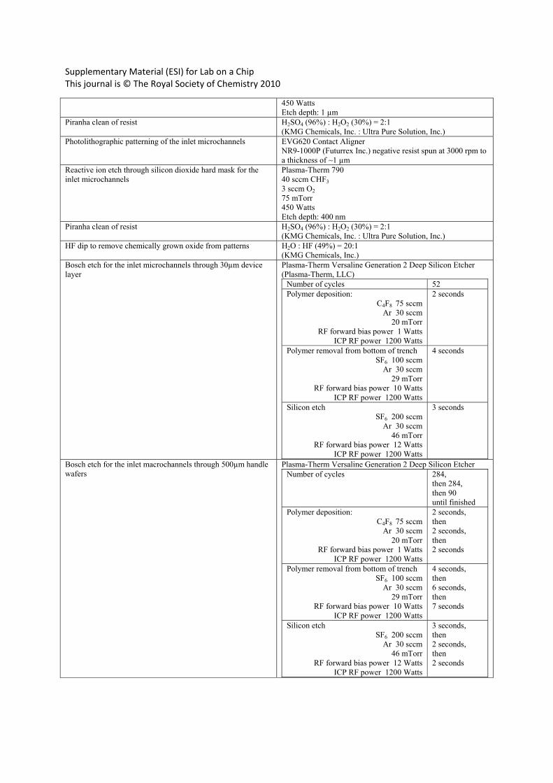
450 Watts Etch depth: 1 µm
Piranha clean of resist H2SO4 (96%) : H2O2 (30%) = 2:1 (KMG Chemicals, Inc. : Ultra Pure Solution, Inc.)
Photolithographic patterning of the inlet microchannels EVG620 Contact Aligner NR9-1000P (Futurrex Inc.) negative resist spun at 3000 rpm to a thickness of ~1 µm
Reactive ion etch through silicon dioxide hard mask for the inlet microchannels
Plasma-Therm 790 40 sccm CHF3 3 sccm O2 75 mTorr 450 Watts Etch depth: 400 nm
Piranha clean of resist H2SO4 (96%) : H2O2 (30%) = 2:1 (KMG Chemicals, Inc. : Ultra Pure Solution, Inc.)
HF dip to remove chemically grown oxide from patterns H2O : HF (49%) = 20:1 (KMG Chemicals, Inc.)
Bosch etch for the inlet microchannels through 30µm device layer
Plasma-Therm Versaline Generation 2 Deep Silicon Etcher (Plasma-Therm, LLC)
Number of cycles 52 Polymer deposition:
C4F8 75 sccm Ar 30 sccm
20 mTorr RF forward bias power 1 Watts
ICP RF power 1200 Watts
2 seconds
Polymer removal from bottom of trench SF6 100 sccm
Ar 30 sccm 29 mTorr
RF forward bias power 10 Watts ICP RF power 1200 Watts
4 seconds
Silicon etch SF6 200 sccm
Ar 30 sccm 46 mTorr
RF forward bias power 12 Watts ICP RF power 1200 Watts
3 seconds
Bosch etch for the inlet macrochannels through 500µm handle wafers
Plasma-Therm Versaline Generation 2 Deep Silicon Etcher Number of cycles 284,
then 284, then 90 until finished
Polymer deposition: C4F8 75 sccm
Ar 30 sccm 20 mTorr
RF forward bias power 1 Watts ICP RF power 1200 Watts
2 seconds, then 2 seconds, then 2 seconds
Polymer removal from bottom of trench SF6 100 sccm
Ar 30 sccm 29 mTorr
RF forward bias power 10 Watts ICP RF power 1200 Watts
4 seconds, then 6 seconds, then 7 seconds
Silicon etch SF6 200 sccm
Ar 30 sccm 46 mTorr
RF forward bias power 12 Watts ICP RF power 1200 Watts
3 seconds, then 2 seconds, then 2 seconds

Supplementary Material (ESI) for Lab on a Chip This journal is © The Royal Society of Chemistry 2010
Piranha clean of sample to remove any Bosch polymer from the patterned SOI substrate
H2SO4 (96%) : H2O2 (30%) = 2:1 (KMG Chemicals, Inc. : Ultra Pure Solution, Inc.)
HF dip to strip LPCVD silicon dioxide masks and exposed buried oxide layer through the inlet macrochannels
H2O:HF(49%) = 10:1 (KMG Chemicals, Inc.)
AFM of nanotrenches (NanoMan VS Scanning Probe Microscope, Veeco Instruments, Inc.)
Scan size: 16 µm Aspect ratio: 8:1 Samples per line: 256 Scan rate: 0.3 Hz Lines: 32 Number of nanotrenches scanned per wafer: 11 (see supplementary Figure. S1)
Nanochannel formation by the anodic bonding of Pyrex to the device layer of the SOI substrate
EVG520IS Semi-Automated Wafer Bonding System (EV Group) 1. High vacuum 2. Heat to 310°C at 20°C/min 3. Pull out separation flags 4. Apply high voltage electrode contact of -1000 V for 20 minutes 5. Purge chamber 6. Cool down
Thinning of the Pyrex capping wafer by lapping Ron Kehl Engineering, San Jose, CA SOI/Pyrex wafer stacks were reversibly bonded to 6 inch in diameter ¼ inch thick stainless steel backing plates using an Alcowax (Nikka Seiko Co., LTD, stripped in isopropyl alcohol)
1. 15 µm diamond slurry for ~480 µm removal in 10 to 20 minute cycles
2. Cerium oxide for final polish Intermediate Pyrex thicknesses were determined by mechanical drop gauge. Final Pyrex thickness was determined by reflectometry Final Pyrex thickness: < 20 µm
Strip of residual bonding wax Isopropyl alcohol Deposition of electroplating seed layer Electron Beam Evaporator (CHA Industries)
Cr deposited at a rate of ~0.5 Å/sec at ~27% power Au deposited at a rate of ~1.1 Å/sec at ~37.6% power Final thickness Cr: 10 nm Final thickness Au: 50 nm
Photolithography of outlet microchannels for electrochemical deposition template
EVG620 Contact Aligner Megaposit SPR220-4.5 positive resist (Rohm and Haas Company) spun at 2500 rpm Stripped in acetone
Electrochemical deposition of nickel Nickel Plating Kit (Caswell Inc.) Includes:
1. Plating tanks 2. Nickel sulphate/Nickel chloride crystals and
saccharin based brightener 3. Nickel anodes 4. Degreaser (unnecessary here) 5. Ceramic heaters 6. Thermostat 7. Pump for filtering and agitation
Final thickness: 4 µm Removal of seed layer from inside outlet microchannel patterns
Etchants obtained from Transene Company, Inc. 1. Gold Etchant TFA (KI-I2 complex) 2. Chromium Etchant TFD (ceric sulfate, nitric acid,
sulphuric acid, water) Deep dielectric etch of the outlet microchannels Plasma-Therm Versaline Generation 2 Deep Dielectric Etcher
1. Time 1860 seconds 2. SF6: 45 sccm

Supplementary Material (ESI) for Lab on a Chip This journal is © The Royal Society of Chemistry 2010
3. O2: 5 sccm 4. Ar: 20 sccm 5. 10 mTorr 6. RF forward bias: 400 Watts 7. RF ICP bias: 1500 Watts
Etch depth: > 20 µm Removal of nickel mask and seed layer Etchants obtained from Transene Company, Inc.
1. Nickel Etchant Type I (FeCl3 .6H2O, HCl, H2O) 2. Gold Etchant TFA (KI-I2 complex) 3. Chromium Etchant TFD (ceric sulfate, nitric acid,
sulphuric acid, water) Dicing to separate individual die Disco 321 Dicing Saw
UV release tape (ProFilm™ DU177E, Advantek, Inc.) Optional: Nanochannel length adjusters:
LPCVD of silicon nitride for selective oxidation mask 800°C 20 sccm H2SiCl2 70sccm NH3 70 mTorr Layer thickness: 65 nm
Photolithography for nanochannel length adjusters EVG620 Contact Aligner (EV Group) AZ 5209 as positive resist (Clariant Corp.) spun at 5000 rpm to a thickness of ~900 nm
Reactive ion etch through silicon nitride for nanochannel length adjusters
Plasma-Therm 790 (Plasma-Therm, LLC) 40 sccm CHF3 3 sccm O2 40 mTorr 400 Watts Etch depth: 65 nm KOH (45%) @ 80°C (Capitol Scientific, Inc.)
Potassium hydroxide etch of nanochannel length adjusters to depth of ~1 µm
or Wet thermal oxidation of nanochannel length adjusters to depth of 0.5 to 1 µm
1050°C 3 L/min H2
HF dip of sample to remove the silicon nitride mask and the selectively grown wet oxide
H2O : HF (49%) = 20:1 (KMG Chemicals, Inc.)
Figure S1. The wafer position of the die whose nanotrenches were sampled by atomic force microscopy prior
to Pyrex capping. 11 scans were recorded for each wafer.

Supplementary Material (ESI) for Lab on a Chip This journal is © The Royal Society of Chemistry 2010
Figure S2. Scanning electron micrographs of the cross section of the nDS showing the top of the inlet
macrochannel, the inlet microchannels, the nanochannel length adjusters, and the outlet microchannels. The samples were embedded using Spurr epoxy resin1, diced along the nanochannel length and surface polished
using diamond lapping films of 1 µm, 0.5 µm, and finally 0.1 µm. The roughness of the epoxy in the macrochannel and the striations on the silicon are due to the lapping process. The outlet microchannels (at
top) were over etched to insure that the nanochannel length adjusters were effectively interfaced. The epoxy resin helped to prevent damage to the fine structure of the membrane but did not eliminate the damage
completely, especially around the length adjusters and the outlet microchannels. The outlet microchannels are smaller in cross section than the inlet microchannels owing to the resist mesas used to template the nickel electroplating process had an aspect ratio of 1 to 1 at 4.5 µm in height and therefore had a significant taper.
The material above the Pyrex is copper tape used to reduce charging during electron scanning.
Testing Apparatus
Gas Test
Table S2 lists the equipment, with suppliers, which comprised the gas testing apparatus.
Figure S3 depicts the gas testing apparatus. Table S2: The gas testing system components
High purity nitrogen tank (99.9999%) Matheson Tri-Gas®
Dual stage regulator Matheson Tri-Gas®, 3120-580
Pressure transducer Omegadyne Inc., PX01C1-200G5T
Gas filter Matheson Tri-Gas®
Precision o-rings Apple Rubber, Lancaster, NY
Hand-held multimeter Fluke 77IV Multimeter
Digital multimeter Agilent model 34410A
6½ digit multimeter
Agilent Technologies, Santa Clara, CA
Stainless steel used for manufacturing the gas test clamping
system and membrane holder
Type SS316L
High pressure regulator for burst testing Victor VIC0386-0814 with a range of 0-4.137MPa

Supplementary Material (ESI) for Lab on a Chip This journal is © The Royal Society of Chemistry 2010
Figure S3. The gas test apparatus.
Gas Test Reproducibility
The reproducibility of the system was also verified by repetitively (10 times) performing
the gas testing with a nanochanneled device2. Figure S4 shows the comparison of the
experimental results. The standard deviation of the experimental results was found to be always
smaller than 1.13*10-4 % which value was calculated in respect of the mean of data. The skew of
the population of data was calculated to evaluate the normality of the data distribution. The small
value of the skew (-0.14) indicates that the data presents a negligible deviation from a Gaussian
distribution. The differences among experimental results were associated to the noise of the
testing system. The results confirm that the noise is significantly smaller than the nominal
repeatability limit of the pressure transducer (± 0.35 %).

Supplementary Material (ESI) for Lab on a Chip This journal is © The Royal Society of Chemistry 2010
Figure S4 – Results of the experimental pressure testing performed 10 times on the same membrane. The value
of the maximum standard deviation S and skew of the data distribution are also listed.
Gas Test Experimental Data Interpolation
The pressure drop is well described by a single exponential decay, consistent with the
solution to a one-dimensional transient problem. The collected pressure data were thus fitted
with an exponential function Dtektp −⋅=)( (correlation coefficient Rc always >0.999). The
interpolation was performed to resample each curve and in a time range of 60 s starting from a
relative pressure of k = 0.31 MPa with Figure S5 showing the results from a single nDS
membrane gas test.

Supplementary Material (ESI) for Lab on a Chip This journal is © The Royal Society of Chemistry 2010
Figure S5. The results of a gas test for a single nDS membrane.
Diffusion Test
Table S3 details the equipment, with suppliers, used for building the diffusion testing
apparatus. Tabel S3: Diffusion testing system components
Stainless steel used for manufacturing both of the chamber
designs for the diffusion testing
Type SS316L
Precision o-rings Apple Rubber, Lancaster, NY
Silicon rubber caps Mocap, Inc., St. Louis, MO
UV macro-cuvette BrandTech Scientific, Inc., Essex, CT
UV-curing epoxy resin OG116-31 Epoxy Technologies, Billerica, MA
A FreeStyle Lite® Blood Glucose Monitoring System Abbott Laboratories
Life Science UV/Vis Spectrophotometer Beckman Coulter DU®730
Spectrophotometer used for the FITC-dextran measurements BMG Labtech GmbH
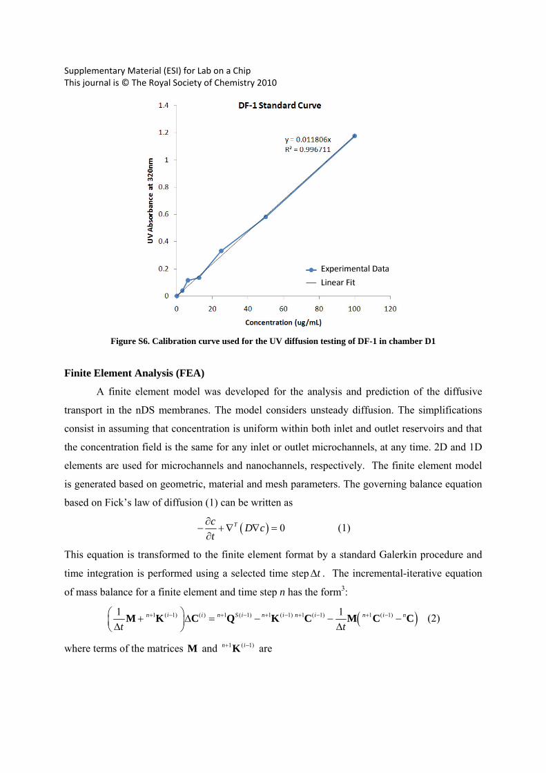
UV Absorbance Standard Curve
Figure S6 shows as an example, the calibration curve for a UV diffusion test with the
diffusion chamber D1.
Supplementary Material (ESI) for Lab on a Chip This journal is © The Royal Society of Chemistry 2010
Figure S6. Calibration curve used for the UV diffusion testing of DF-1 in chamber D1
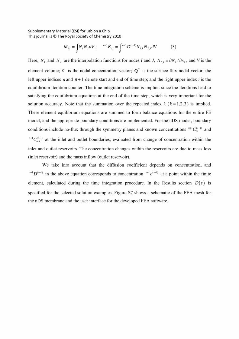
Finite Element Analysis (FEA)
A finite element model was developed for the analysis and prediction of the diffusive
transport in the nDS membranes. The model considers unsteady diffusion. The simplifications
consist in assuming that concentration is uniform within both inlet and outlet reservoirs and that
the concentration field is the same for any inlet or outlet microchannels, at any time. 2D and 1D
elements are used for microchannels and nanochannels, respectively. The finite element model
is generated based on geometric, material and mesh parameters. The governing balance equation
based on Fick’s law of diffusion (1) can be written as
( ) 0Tc D ct
∂− +∇ ∇ =∂
(1)
This equation is transformed to the finite element format by a standard Galerkin procedure and
time integration is performed using a selected time step tΔ . The incremental-iterative equation
of mass balance for a finite element and time step n has the form3:
( )1 ( 1) ( ) 1 ( 1) 1 ( 1) 1 ( 1) 1 ( 1)1 1n i i n S i n i n i n i n
t t+ − + − + − + − + −⎛ ⎞+ Δ = − − −⎜ ⎟Δ Δ⎝ ⎠
M K C Q K C M C C
(2)
where terms of the matrices M and 1 ( 1)n i+ −K are
Supplementary Material (ESI) for Lab on a Chip This journal is © The Royal Society of Chemistry 2010
IJ I JV
M N N dV= ∫ , 1 1 ( 1), ,
n n iIJ I k J k
V
K D N N dV+ + −= ∫ (3)
Here, IN and JN are the interpolation functions for nodes I and J, , /I k I kN N x≡ ∂ ∂ , and V is the
element volume; C is the nodal concentration vector; SQ is the surface flux nodal vector; the
left upper indices n and 1n + denote start and end of time step; and the right upper index i is the
equilibrium iteration counter. The time integration scheme is implicit since the iterations lead to
satisfying the equilibrium equations at the end of the time step, which is very important for the
solution accuracy. Note that the summation over the repeated index k ( 1,2,3k = ) is implied.
These element equilibrium equations are summed to form balance equations for the entire FE
model, and the appropriate boundary conditions are implemented. For the nDS model, boundary
conditions include no-flux through the symmetry planes and known concentrations 1 ( 1)n iinC+ − and
1 ( 1)n ioutC+ − at the inlet and outlet boundaries, evaluated from change of concentration within the
inlet and outlet reservoirs. The concentration changes within the reservoirs are due to mass loss
(inlet reservoir) and the mass inflow (outlet reservoir).
We take into account that the diffusion coefficient depends on concentration, and 1 ( 1)n iD+ − in the above equation corresponds to concentration 1 ( 1)n ic+ − at a point within the finite
element, calculated during the time integration procedure. In the Results section ( )D c is
specified for the selected solution examples. Figure S7 shows a schematic of the FEA mesh for
the nDS membrane and the user interface for the developed FEA software.

Supplementary Material (ESI) for Lab on a Chip This journal is © The Royal Society of Chemistry 2010
Figure S7. Schematic of the FEA mesh for the nDS membrane and user interface for the developed FEA
software.
Further Acknowledgments
The authors would also like to thank the following individuals:
Mr. Paul Sadlek, Mr. Dwarakanath Geerpuram, and Mr. Brad Reelfs at Plasma-Therm, LLC., St.
Petersburg, FL,
Mr. Tian Tang and Mr. Karl White at EV Group, Tempe, AZ,
Dr. Marylene Pallard at the Microelectronics Research Center, University of Texas at Austin,
Austin, TX,
Mr. Wallace Martin, Dr. Gordon Pollack, Dr. Roger Robbins, Mr. Arnold Duenes, and Mr. Scott
Riekena at the Cleanroom Research Laboratory, University of Texas at Dallas, Dallas, TX,
Mr. Meredith Metzler, Mr. Vince Genoa, Dr. Rob Ilic, Mr. John Grazul, Mr. Daron Westly, Mr.
Michael Skvarla, and Mr. Dan Woodie at the Cornell Nanofabrication Facility, Cornell
University, Ithaca, NY,
Mr. Noah Clay and Mr. John Tsakirgis at the Center for Nanoscale Systems, Harvard University,
Cambridge, MA,

Supplementary Material (ESI) for Lab on a Chip This journal is © The Royal Society of Chemistry 2010
Dr. Mary Tang at the Stanford Nanofabrication Facility, Stanford University, Palo Alto, CA,
Dr. William M. Lackowski (formerly of), and Mr. Michael Tiner at the Center for Nano and
Molecular Sciences, University of Texas at Austin, Austin, TX,
Erika Zabre for her support in the experimental analysis,
Dr. William Neil Everett and Mr. Ciro Chiappini for useful discussions and editing acumen.
Supplementary References
1. A. R. Spurr, J. Ultrastruct. Res., 1969, 26, 31-43. 2. A. Grattoni, E. De Rosa, S. Ferrati, Z. Wang, A. Gianesini, X. Liu, F. Hussain, R. Goodall, and
M. Ferrari, J. Micromech. Microeng., 2009, 19, 115018. 3. M. Kojić, N. Filipović, B. Stojanović, and N. Kojić, Computer Modeling in Bioengineering:
Theoretical background, examples and software, John Wiley & Sons, 2008.