supplementary information - media.nature.com · nature energy | 8 .10/gy.20.xx ulementary...
TRANSCRIPT

In the format provided by the authors and unedited.
1
Supplementary Information for
Enhanced Electron Extraction Using SnO2 for
High-Efficiency Planar-Structure HC(NH2)2PbI3-based
Perovskite Solar Cells
Qi Jiang, Liuqi Zhang, Haolin Wang, Xiaolei Yang, Junhua Meng, Heng Liu, Zhigang Yin,
Jinliang Wu, Xingwang Zhang,* Jingbi You*
Key Lab of Semiconductor Materials Science, Beijing Key Laboratory of Low Dimensional
Semiconductor Materials and Devices, Institute of Semiconductors, Chinese Academy of
Sciences, Beijing 100083, P. R. China. *e-mail: [email protected] (J. Y.); [email protected]
(X. Z.)
© 2016 Macmillan Publishers Limited, part of Springer Nature. All rights reserved.
SUPPLEMENTARY INFORMATIONARTICLE NUMBER: 16177 | DOI: 10.1038/NENERGY.2016.177
NATURE ENERGY | www.nature.com/natureenergy 1
2
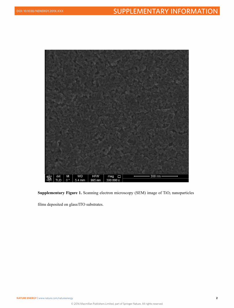
Supplementary Figure 1. Scanning electron microscopy (SEM) image of TiO2 nanoparticles
films deposited on glass/ITO substrates.
© 2016 Macmillan Publishers Limited, part of Springer Nature. All rights reserved.
NATURE ENERGY | www.nature.com/natureenergy 2
SUPPLEMENTARY INFORMATIONDOI: 10.1038/NENERGY.201X.XXX

3
Supplementary Figure 2. XPS of SnO2 nanoparticles. (a) Sn 3d core level (CL) spectrum in
SnO2, (b) O 1s core level (CL) spectrum in SnO2 layer.
© 2016 Macmillan Publishers Limited, part of Springer Nature. All rights reserved.
NATURE ENERGY | www.nature.com/natureenergy 3
SUPPLEMENTARY INFORMATIONDOI: 10.1038/NENERGY.201X.XXX

4
Supplementary Figure 3. XPS of TiO2 nanoparticles. (a) Ti 2p core level (CL) spectrum in
TiO2, (b) O 1s core level (CL) spectrum in TiO2 layer.
© 2016 Macmillan Publishers Limited, part of Springer Nature. All rights reserved.
NATURE ENERGY | www.nature.com/natureenergy 4
SUPPLEMENTARY INFORMATIONDOI: 10.1038/NENERGY.201X.XXX
5
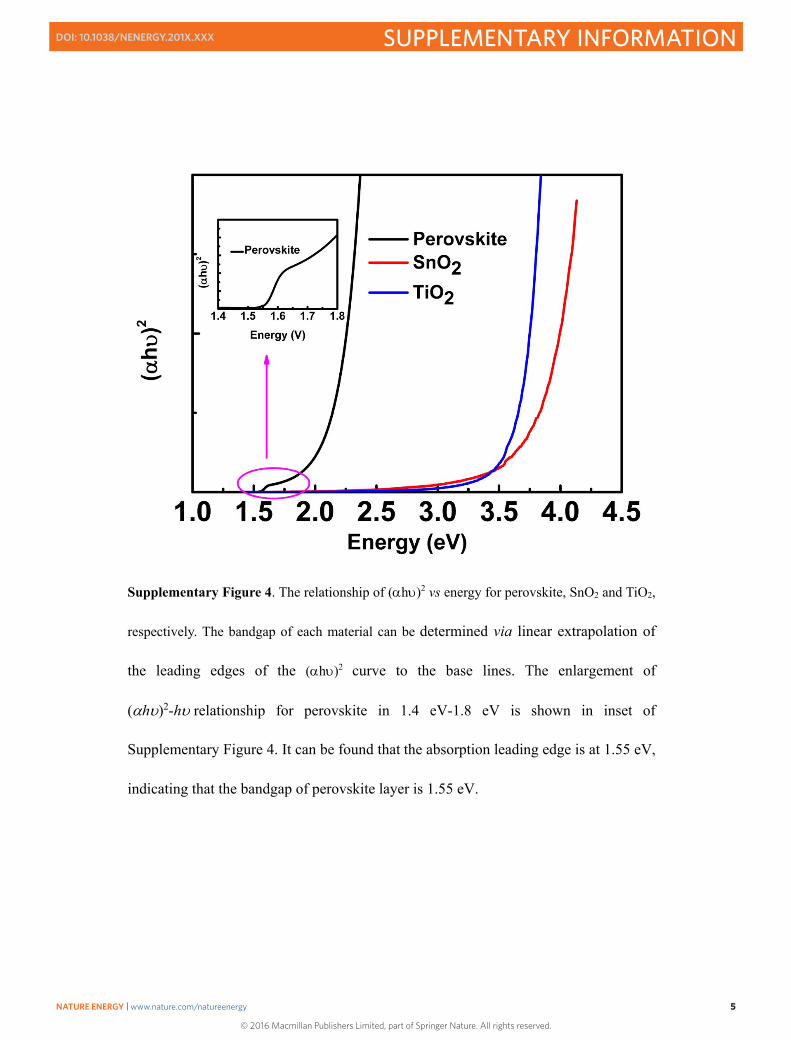
Supplementary Figure 4. The relationship of (h)2 vs energy for perovskite, SnO2 and TiO2,
respectively. The bandgap of each material can be determined via linear extrapolation of
the leading edges of the (h)2 curve to the base lines. The enlargement of
(h)2-hrelationship for perovskite in 1.4 eV-1.8 eV is shown in inset of
Supplementary Figure 4. It can be found that the absorption leading edge is at 1.55 eV,
indicating that the bandgap of perovskite layer is 1.55 eV.
© 2016 Macmillan Publishers Limited, part of Springer Nature. All rights reserved.
NATURE ENERGY | www.nature.com/natureenergy 5
SUPPLEMENTARY INFORMATIONDOI: 10.1038/NENERGY.201X.XXX
6
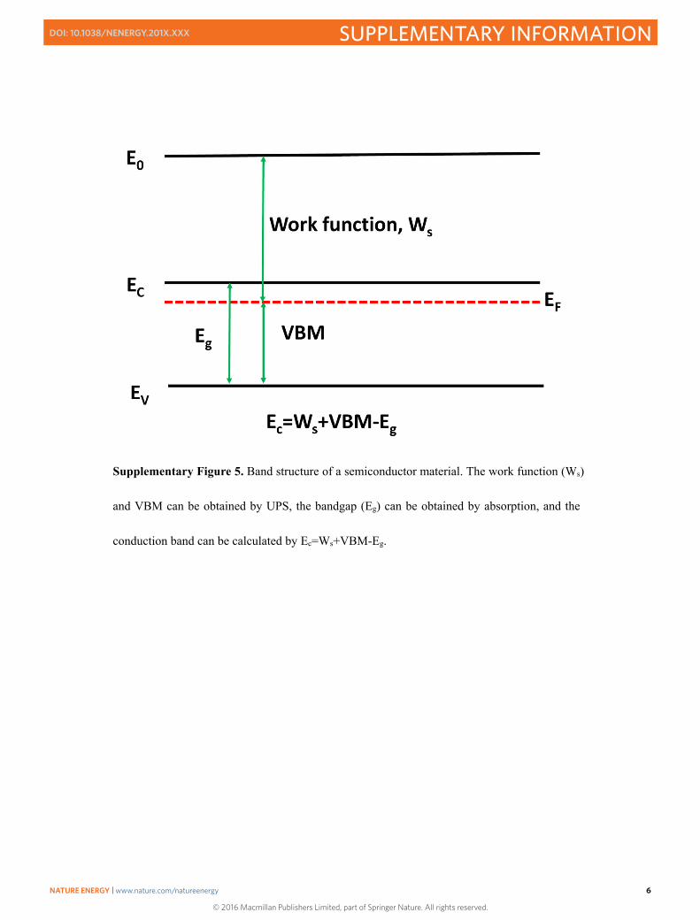
Supplementary Figure 5. Band structure of a semiconductor material. The work function (Ws)
and VBM can be obtained by UPS, the bandgap (Eg) can be obtained by absorption, and the
conduction band can be calculated by Ec=Ws+VBM-Eg.
© 2016 Macmillan Publishers Limited, part of Springer Nature. All rights reserved.
NATURE ENERGY | www.nature.com/natureenergy 6
SUPPLEMENTARY INFORMATIONDOI: 10.1038/NENERGY.201X.XXX

7
Supplementary Figure 6. Several possible band alignment between perovskite and TiO2,
SnO2 based on the deeper conduction band of SnO2. (a) is plotted based on our
measurement results, if band bending existed due to the interface traps or charge
accumulations, the band diagram should be modified to be (b), even in this case, the SnO2
based device still own better charge transfer. (c) and (d) are impossible, if the conduction
band of SnO2 aligned with perovskite such like these, the open circuit voltage will be lost a lot,
in fact, the Voc of our devices showed good open circuit voltage. Furthermore, in case of (c) or
(d), the charge transfer from perovskite into TiO2 should be efficient, and significant
photoluminescence (PL) quench should be observed.
© 2016 Macmillan Publishers Limited, part of Springer Nature. All rights reserved.
NATURE ENERGY | www.nature.com/natureenergy 7
SUPPLEMENTARY INFORMATIONDOI: 10.1038/NENERGY.201X.XXX

8
Supplementary Figure 7. Comparison of charge transport properties from the devices using
SnO2 and TiO2, respectively. Higher injection current indicated better charge transport
properties.
© 2016 Macmillan Publishers Limited, part of Springer Nature. All rights reserved.
NATURE ENERGY | www.nature.com/natureenergy 8
SUPPLEMENTARY INFORMATIONDOI: 10.1038/NENERGY.201X.XXX
9
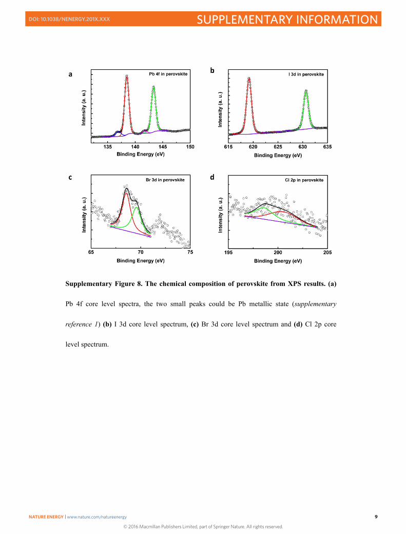
Supplementary Figure 8. The chemical composition of perovskite from XPS results. (a)
Pb 4f core level spectra, the two small peaks could be Pb metallic state (supplementary
reference 1) (b) I 3d core level spectrum, (c) Br 3d core level spectrum and (d) Cl 2p core
level spectrum.
© 2016 Macmillan Publishers Limited, part of Springer Nature. All rights reserved.
NATURE ENERGY | www.nature.com/natureenergy 9
SUPPLEMENTARY INFORMATIONDOI: 10.1038/NENERGY.201X.XXX

10
Supplementary Figure 9. Scanning electron microscopy (SEM) image of perovskite film
annealing under different temperature (a) 135oC and (b) 150oC in large scale size. The scale
bars are 5m.
© 2016 Macmillan Publishers Limited, part of Springer Nature. All rights reserved.
NATURE ENERGY | www.nature.com/natureenergy 10
SUPPLEMENTARY INFORMATIONDOI: 10.1038/NENERGY.201X.XXX

11
Supplementary Figure 10. (a) and (b)Scanning electron microscopy (SEM) image of
perovskite film annealing at 150oC for 20 min, the scale bar are 200 nm. (c) and (d) Energy
disperse X-ray (EDX) analysis for the two labelled area shown in (a) “white phase” and (b)
“dark phase”, respectively. From EDX results, the “white phase” area showed the less Pb:I
ratio (Pb:I=1:2.61) than that of dark phase area (Pb:I=1:2.87), indicating that the white phase
could be PbI2 rich area. For FAPbI3 (Pb:I=1:3) and PbI2 (Pb:I=1:2).
© 2016 Macmillan Publishers Limited, part of Springer Nature. All rights reserved.
NATURE ENERGY | www.nature.com/natureenergy 11
SUPPLEMENTARY INFORMATIONDOI: 10.1038/NENERGY.201X.XXX
12
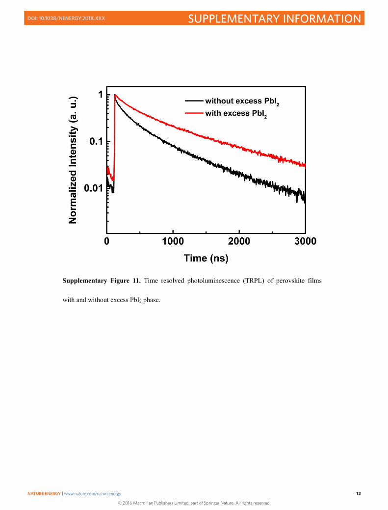
Supplementary Figure 11. Time resolved photoluminescence (TRPL) of perovskite films
with and without excess PbI2 phase.
© 2016 Macmillan Publishers Limited, part of Springer Nature. All rights reserved.
NATURE ENERGY | www.nature.com/natureenergy 12
SUPPLEMENTARY INFORMATIONDOI: 10.1038/NENERGY.201X.XXX
13
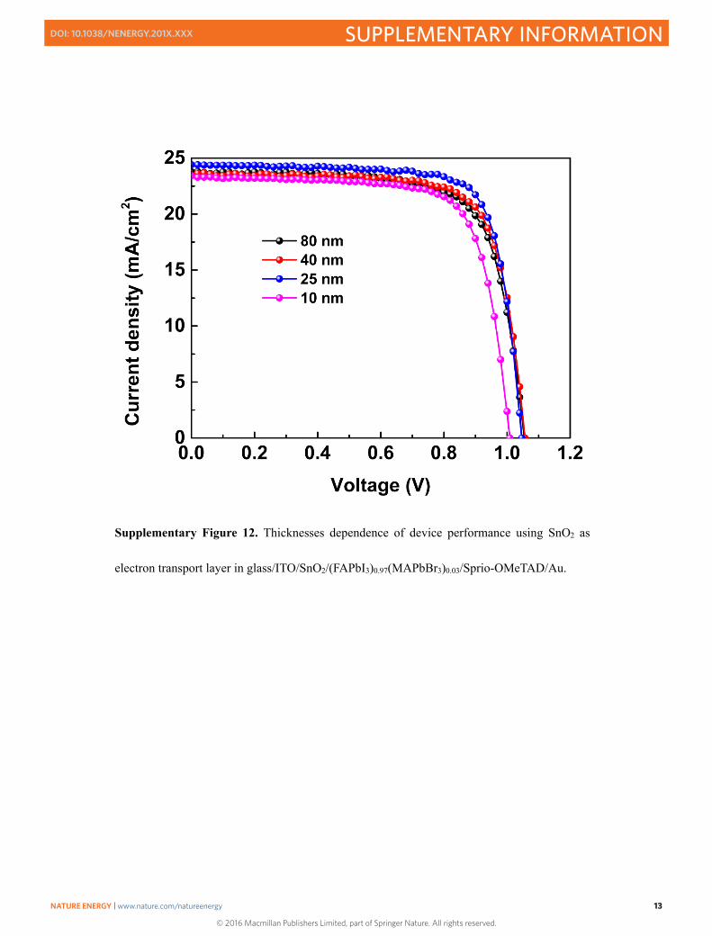
Supplementary Figure 12. Thicknesses dependence of device performance using SnO2 as
electron transport layer in glass/ITO/SnO2/(FAPbI3)0.97(MAPbBr3)0.03/Sprio-OMeTAD/Au.
© 2016 Macmillan Publishers Limited, part of Springer Nature. All rights reserved.
NATURE ENERGY | www.nature.com/natureenergy 13
SUPPLEMENTARY INFORMATIONDOI: 10.1038/NENERGY.201X.XXX
14
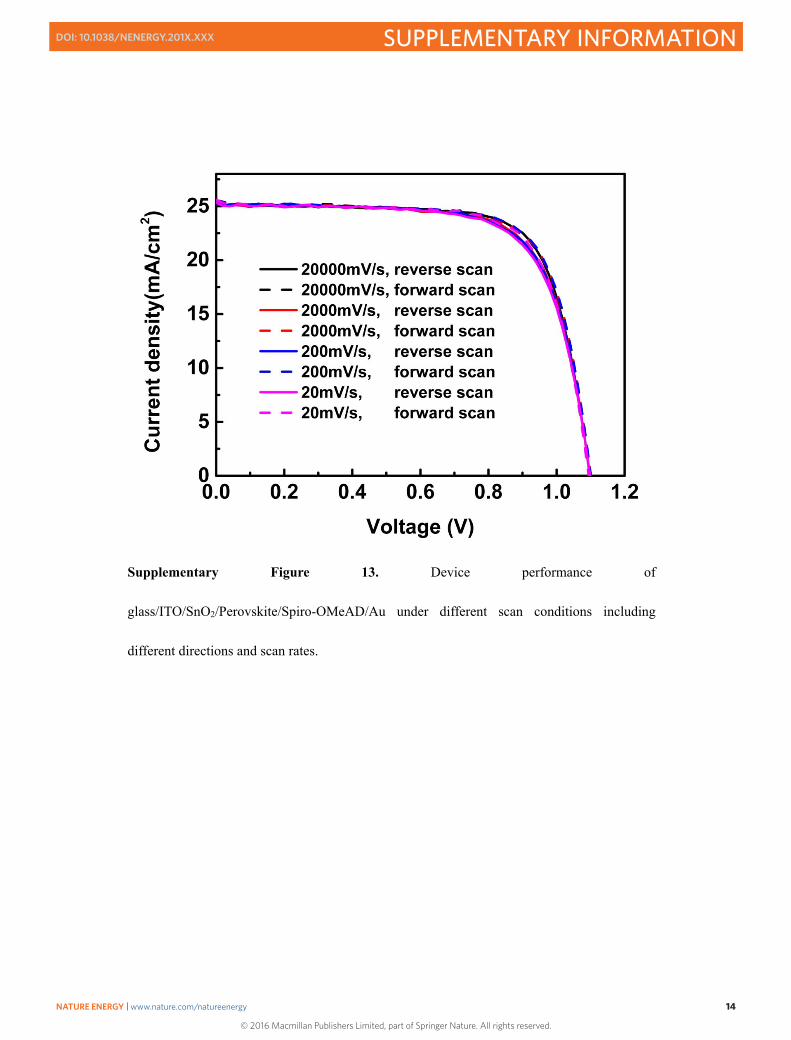
Supplementary Figure 13. Device performance of
glass/ITO/SnO2/Perovskite/Spiro-OMeAD/Au under different scan conditions including
different directions and scan rates.
© 2016 Macmillan Publishers Limited, part of Springer Nature. All rights reserved.
NATURE ENERGY | www.nature.com/natureenergy 14
SUPPLEMENTARY INFORMATIONDOI: 10.1038/NENERGY.201X.XXX
15
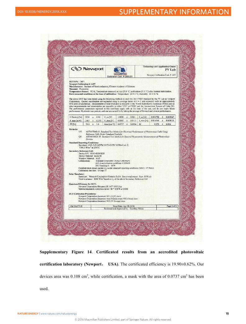
Supplementary Figure 14. Certificated results from an accredited photovoltaic
certification laboratory (Newport, USA). The certificated efficiency is 19.90±0.62%. Our
devices area was 0.108 cm2, while certification, a mask with the area of 0.0737 cm2 has been
used.
© 2016 Macmillan Publishers Limited, part of Springer Nature. All rights reserved.
NATURE ENERGY | www.nature.com/natureenergy 15
SUPPLEMENTARY INFORMATIONDOI: 10.1038/NENERGY.201X.XXX
16
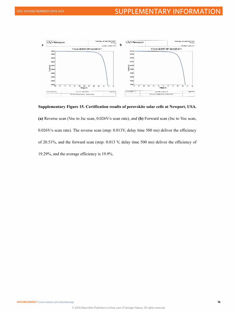
Supplementary Figure 15. Certification results of perovskite solar cells at Newport, USA.
(a) Reverse scan (Voc to Jsc scan, 0.026V/s scan rate), and (b) Forward scan (Jsc to Voc scan,
0.026V/s scan rate). The reverse scan (step: 0.013V, delay time 500 ms) deliver the efficiency
of 20.51%, and the forward scan (step: 0.013 V, delay time 500 ms) deliver the efficiency of
19.29%, and the average efficiency is 19.9%.
© 2016 Macmillan Publishers Limited, part of Springer Nature. All rights reserved.
NATURE ENERGY | www.nature.com/natureenergy 16
SUPPLEMENTARY INFORMATIONDOI: 10.1038/NENERGY.201X.XXX

17
Supplementary Figure 16. Devices stability stored in dry air without encapsulation. Here, we
showed stability data for four devices.
© 2016 Macmillan Publishers Limited, part of Springer Nature. All rights reserved.
NATURE ENERGY | www.nature.com/natureenergy 17
SUPPLEMENTARY INFORMATIONDOI: 10.1038/NENERGY.201X.XXX
18
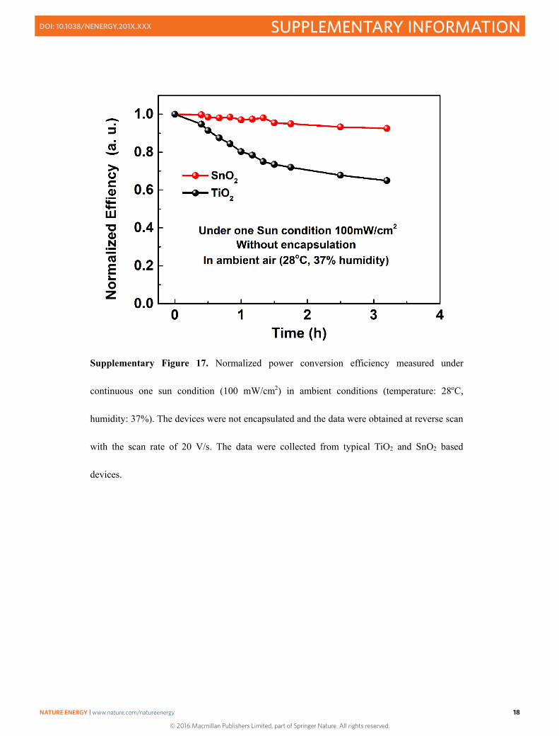
Supplementary Figure 17. Normalized power conversion efficiency measured under
continuous one sun condition (100 mW/cm2) in ambient conditions (temperature: 28oC,
humidity: 37%). The devices were not encapsulated and the data were obtained at reverse scan
with the scan rate of 20 V/s. The data were collected from typical TiO2 and SnO2 based
devices.
© 2016 Macmillan Publishers Limited, part of Springer Nature. All rights reserved.
NATURE ENERGY | www.nature.com/natureenergy 18
SUPPLEMENTARY INFORMATIONDOI: 10.1038/NENERGY.201X.XXX
19
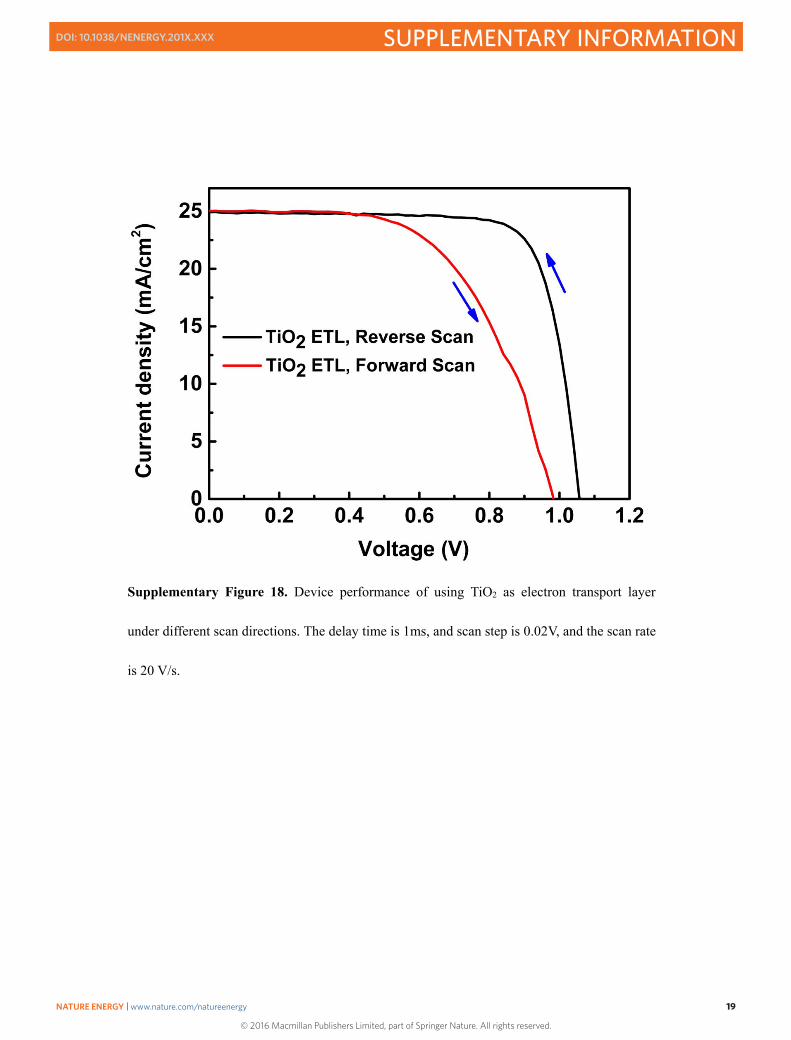
Supplementary Figure 18. Device performance of using TiO2 as electron transport layer
under different scan directions. The delay time is 1ms, and scan step is 0.02V, and the scan rate
is 20 V/s.
© 2016 Macmillan Publishers Limited, part of Springer Nature. All rights reserved.
NATURE ENERGY | www.nature.com/natureenergy 19
SUPPLEMENTARY INFORMATIONDOI: 10.1038/NENERGY.201X.XXX
20
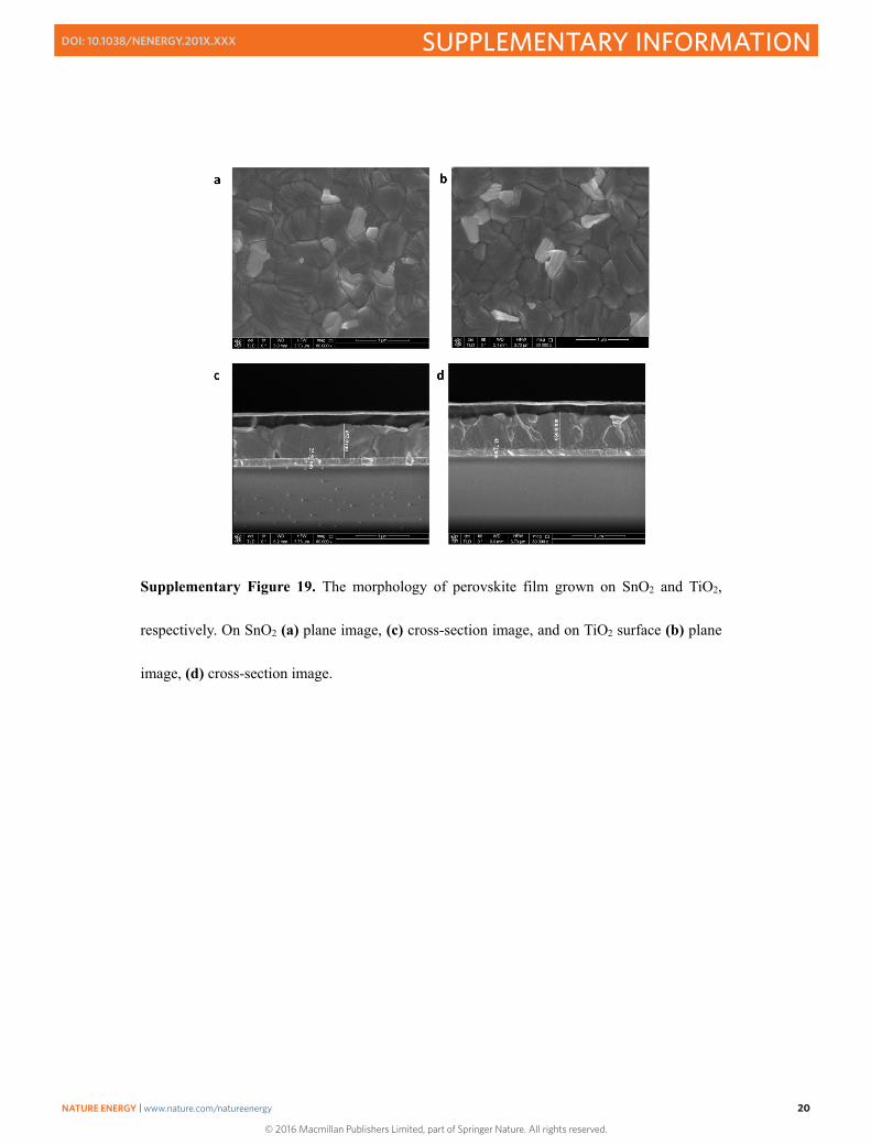
Supplementary Figure 19. The morphology of perovskite film grown on SnO2 and TiO2,
respectively. On SnO2 (a) plane image, (c) cross-section image, and on TiO2 surface (b) plane
image, (d) cross-section image.
© 2016 Macmillan Publishers Limited, part of Springer Nature. All rights reserved.
NATURE ENERGY | www.nature.com/natureenergy 20
SUPPLEMENTARY INFORMATIONDOI: 10.1038/NENERGY.201X.XXX
21
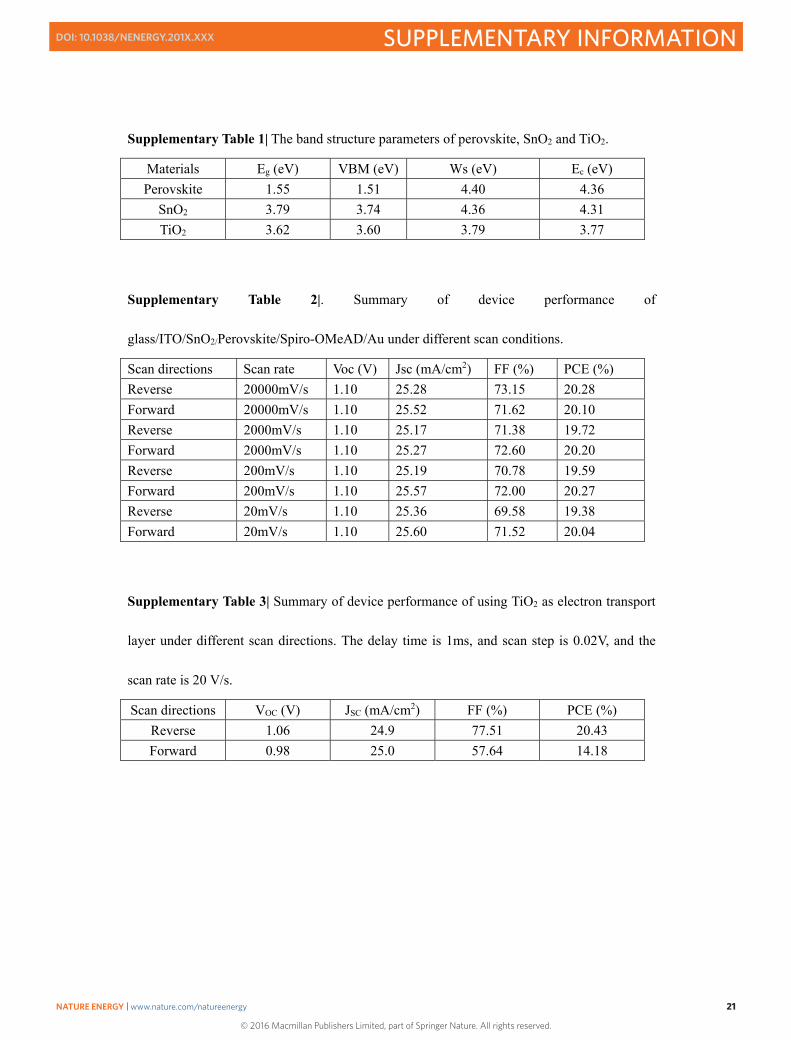
Supplementary Table 1| The band structure parameters of perovskite, SnO2 and TiO2.
Materials Eg (eV) VBM (eV) Ws (eV) Ec (eV) Perovskite 1.55 1.51 4.40 4.36
SnO2 3.79 3.74 4.36 4.31 TiO2 3.62 3.60 3.79 3.77
Supplementary Table 2|. Summary of device performance of
glass/ITO/SnO2/Perovskite/Spiro-OMeAD/Au under different scan conditions.
Scan directions Scan rate Voc (V) Jsc (mA/cm2) FF (%) PCE (%) Reverse 20000mV/s 1.10 25.28 73.15 20.28 Forward 20000mV/s 1.10 25.52 71.62 20.10 Reverse 2000mV/s 1.10 25.17 71.38 19.72 Forward 2000mV/s 1.10 25.27 72.60 20.20 Reverse 200mV/s 1.10 25.19 70.78 19.59 Forward 200mV/s 1.10 25.57 72.00 20.27 Reverse 20mV/s 1.10 25.36 69.58 19.38 Forward 20mV/s 1.10 25.60 71.52 20.04
Supplementary Table 3| Summary of device performance of using TiO2 as electron transport
layer under different scan directions. The delay time is 1ms, and scan step is 0.02V, and the
scan rate is 20 V/s.
Scan directions VOC (V) JSC (mA/cm2) FF (%) PCE (%) Reverse 1.06 24.9 77.51 20.43 Forward 0.98 25.0 57.64 14.18
© 2016 Macmillan Publishers Limited, part of Springer Nature. All rights reserved.
NATURE ENERGY | www.nature.com/natureenergy 21
SUPPLEMENTARY INFORMATIONDOI: 10.1038/NENERGY.201X.XXX

22
Supplementary References:
1. W. Zhang et al. Enhanced optoelectronic quality of perovskite thin films with
hypophosphorous acid for planar heterojunction solar cells. Nat. Communications, 6,
10030 (2015).
© 2016 Macmillan Publishers Limited, part of Springer Nature. All rights reserved.
NATURE ENERGY | www.nature.com/natureenergy 22
SUPPLEMENTARY INFORMATIONDOI: 10.1038/NENERGY.201X.XXX