supplementary materials title: selective mechanical
TRANSCRIPT
1
Supplementary Materials
Title: Selective Mechanical Transfer of Graphene from Seed Copper Foil Using
Peel Rate Effects
Authors: Seung Ryul Na1†, Ji Won Suk5†, Li Tao3, Deji Akinwande3, Rodney S. Ruoff2,4, Rui Huang1,
Kenneth M. Liechti1*
Affiliations:
1 Department of Aerospace Engineering and Engineering Mechanics
Research Center for the Mechanics of Solids, Structures and Materials
2 Department of Mechanical Engineering and The Materials Science and Engineering Program
3Department of Electrical and Computer Engineering
The University of Texas at Austin
Austin, Texas 78712
4 Institute of Basic Sciences Center for Multidimensional Carbon Materials & Department of
Chemistry and School of Materials Science and Engineering
Ulsan National Institute of Science and Technology, Ulsan 689-798, Republic of Korea
5 School of Mechanical Engineering, Sungkyunkwan University, Suwon, 440-746, Republic of Korea
† S.R. Na and J.W. Suk contributed equally to this work.
*Correspondence to: [email protected]

2
1. Preparation of Silicon Strips
Silicon strips (5x40 mm) were cut from 100 mm Si(111), P/Bo-doped and double-side-polished (DSP)
wafers (291±5 µm thick) using a dicing machine (Disco DAD 321). Each silicon strip was cleaned in an
ultrasonic-bath filled with de-ionized water for 30 minutes to remove any debris that was formed during
the dicing process. The silicon strips were then dipped in a piranha solution (5 mL in hydrogen peroxide
and 15 mL in sulfuric acid) for 30 minutes to remove any organic residue which may degrade the
adhesion of the silicon and epoxy. The silicon strips were then cleaned in a de-ionized water bath and
any water residue was blown out in a stream of dry nitrogen. Finally, the piranha-treated silicon strips
were stored in a glass tube filled with dry nitrogen.
2. Preparation of epoxy
The epoxy (EP30, Master Bond) resin and hardener were mixed in a four to one ratio by weight. Any
bubbles created during the mixing process were removed in a vacuum jar for 10 minutes. The viscosity
of the mixture remained low enough, for about 20 minutes, for spreading.
3. Fabrication of sandwich specimens
The graphene was grown by chemical vapor deposition (CVD) on 5x5 cm copper foils (Alfa Aesar,
CAS:7440-50-8, LOT No. 46365) that were wrapped around a quartz tube. 1 The graphene-coated foils
were then flattened on 100-mm silicon DSP wafers (Fig. S1a). The degassed epoxy was applied over the
entire surface of the first silicon strip (Fig. S1b) and the epoxy surface of the coated strip was placed in
contact with the graphene (Fig. S1c) and subjected to a uniform pressure in order to produce a uniform
epoxy layer. This assembly was cured at 100 °C for two hours, following the manufacturer’s
recommendations. Graphene/copper/graphene/epoxy/silicon strips were cut from the assembly, ready
for the application of the second epoxy-coated silicon strip (Fig. S1d). The epoxy only partially covered
the second silicon strip, which was then placed in contact with the remaining graphene surface so as to
form a 2-cm long notch in the region without epoxy (Fig. S1e). The same curing conditions were applied
and resulted in a laminate (silicon/epoxy/graphene/copper/graphene/epoxy/silicon) with a 1-cm long
notch, which acted as a blunt initial crack. Finally, two aluminum loading tabs were bonded to the top
and bottom silicon surfaces at the cracked end of the laminate (Fig. S1f).

3
Figure S1: Outlines the steps that were taken to fabricate the laminate: (a) Copper foils (5 ×5 cm) with
graphene on both sides were flattened on a silicon wafer. (b) Epoxy was applied over the entire surface
of the first set of silicon strips. (c) Four to six epoxy-coated silicon strips were placed on the flattened foil
and a uniform pressure was applied for one minute before the assembly was cured at 100 °C for two
hours. (d) The assembly was then cut between the silicon strips and another set of silicon strips partially
coated with epoxy were prepared. (e) The two sets of strips were brought together under uniform
pressure for one minute and the assembly was cured for two hours at 100 °C to form a specimen with a
blunt initial crack at in the region with no epoxy. (f) Bonding of aluminum loading tabs.

4
4. Definition of bimaterial corners
When the specimens were fabricated, the top epoxy layer (Fig. S2) was approximately 20 µm thick,
which meant that the initial crack was quite blunt. More precisely, the local geometry consisted of
epoxy/graphene and epoxy/silicon bimaterial corners, each having a particular stress concentration 2.
Figure S2: A schematic of the bimaterial corners formed at the terminus of the top epoxy layer.

5
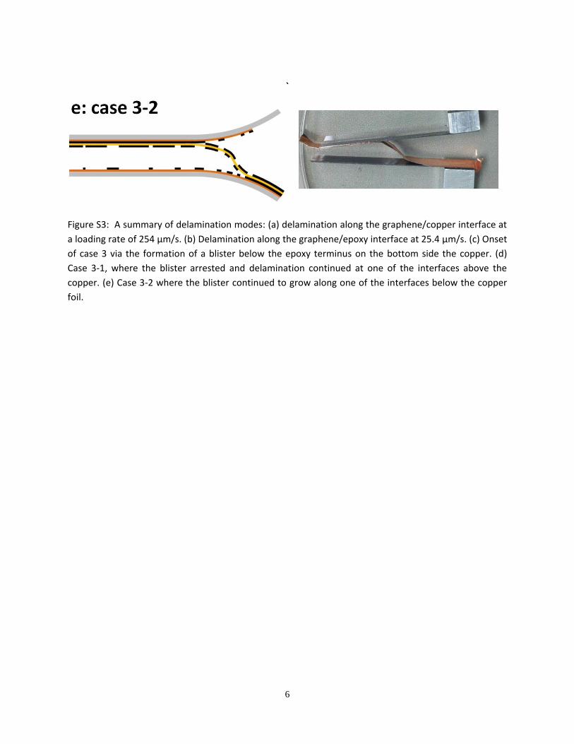
5. Identification of Delamination Modes
The three major delamination modes observed in this study were designated case 1, case 2 and case 3.
Case 1 (Fig. S3a) was pure delamination along the graphene/copper interface and was dominant when
the applied loading rate was 254 µm/s. Case 2, delamination along the epoxy/graphene interface,
occurred when the applied displacement rate was reduced to 25.4 µm/s (Fig. S3b). Under this condition,
graphene still remained on the copper foil. Case 3 occurred at all rates and always involved the
formation of a blister below the copper foil (Fig. S3c), probably due to slightly lower adhesion, but its
presence allowed subdivision into cases 3-1 (Fig. S3d) and 3-2 (Fig. S3e). Once a copper blister was
formed, case 3-1 arose when delaminations could develop above the copper foil, which arrested further
growth of the blister. Alternatively, it was possible for the blisters to grow below the copper without any
further delamination growth above it; this was case 3-2. In both cases, graphene was transferred to
epoxy, but there were regions where the graphene was continuous and others where it was only
present as patches.
6
`
Figure S3: A summary of delamination modes: (a) delamination along the graphene/copper interface at
a loading rate of 254 μm/s. (b) Delamination along the graphene/epoxy interface at 25.4 μm/s. (c) Onset
of case 3 via the formation of a blister below the epoxy terminus on the bottom side the copper. (d)
Case 3-1, where the blister arrested and delamination continued at one of the interfaces above the
copper. (e) Case 3-2 where the blister continued to grow along one of the interfaces below the copper
foil.

7
6. High resolution SEM image of graphene transferred to epoxy
Figure S4a is a high resolution image taken of graphene on epoxy following delamination along the
graphene/copper interface. When epoxy was used to form the sandwich specimens, its low viscosity
allowed it to replicate the steps (Fig. 6) on the surface of the graphene-coated copper foil. As a result,
steps, ad-layers and wrinkles can be observed after mechanical transfer. In addition, there were regions
of charging from epoxy islands which were exposed by holes in the graphene. In such regions there was
probably no contact between the epoxy and graphene due to micro voids at or near the interface so
that the graphene could not be removed from the copper. This scenario is depicted in Figure S4b.

8
Figure S4: High resolution image of graphene transferred to epoxy: (a) The SEM image shows steps, ad-
layers, wrinkles and epoxy islands or holes in the graphene. (b) Schematic of the formation of holes in
the graphene due to (assumed) micro voids in the epoxy.

9
7. Decomposition of Raman peaks
The Raman spectra presented in this study were obtained with a WITec Alpha 300 micro-Raman
confocal microscope operating at a wavelength of 488 nm. The spectra shown below (Fig. S5) were
obtained from a bare epoxy layer and a graphene-coated epoxy layer following successful transfer. The
spectrum for bare epoxy had a major peak at 1605 cm-1 which is close to the G band for graphene. The
spectrum for graphene on epoxy had a broad peak near the G band and a peak at 2691 cm-1,
corresponding to the 2D band. When the bare epoxy spectrum was subtracted from the total response,
the subtracted spectrum had a very sharp peak at 1587 cm-1, which is within the accepted range for the
G band of graphene. The subtracted spectrum retained the 2D peak that was seen in the total response
because there was no contribution from the epoxy. The ratio 2D / GI I for the subtracted spectrum was
approximately 1.3, which is still less than the usual value of 3 for monolayer graphene on SiO2 substrates.
The reason for this difference may be due to chemical doping from the epoxy layer.
Figure S5: Raman spectra for graphene/epoxy (black), bare epoxy (red) and the subtracted response
(blue).

10
8. Facture analysis
Simple beam theory predicts the load-displacement response of the double cantilever beam specimen
(Fig. 1a) as
3
38
EbhP
a
, (S1)
where P and are the load and applied displacement, respectively, E is the in-plane Young’s
modulus (169 GPa) of the silicon strips whose upper and lower surfaces were Si(111), b and h are the
width (5±0.2 mm) and thickness (nominally 291±5 µm) of the silicon strips and a is the crack length,
measured from the point of load application to the crack front (Fig. 1a). The stiffness (or slope) /P
of the load-displacement response in Equation (S1) depends on the crack length and should remain
constant until the crack grows. The predicted response is compared with the measured response for a
delamination along the graphene/copper interface in Figure 2b. The measured response under an
applied displacement rate of 254.0 µm/s was obtained from three separate load/unload cycles on the
same specimen. The first cycle was for a crack length of 14.5 mm corresponding to the region of the
upper silicon that was not bonded to the copper. Initiation of the delamination occurred just before the
peak load and once some growth (increase in a ) had occurred, the delamination was arrested by
unloading the specimen, by which time the crack length was 21.5 mm. Reloading the specimen for the
second cycle resulted in a lower stiffness (as expected from Equation (S1) due to the longer
delamination) and more gradual delamination, most likely due to the fact that the arrested crack was
sharper than the original crack formed by the epoxy terminus. The subsequent unloading and reloading
yielded the third response, starting at a delamination length of 30.0 mm. For the first cycle, the stiffness
of the loading portion of the response prior to any delamination was captured by the simple beam
theory prediction (designated LEFM 1) embodied in Equation (S1). The same was true for the other two
experiments although the comparison was omitted in Figure 2b for the sake of clarity. The simple beam

11
theory was then used to determine the elastic strain energy available for delamination or the energy
release rate G , which is given by
2 2
32
12a
E
PG
b h . (S2)
Thus, prior to the onset of delamination, the energy release rate increases with increasing load until
crack growth initiates, at which time the load decreases while the crack length increases. In accordance
with the simplest criterion for delamination growth, this occurs when the energy release rate reaches
the adhesion energy ss of the interface and the subsequent load-displacement response follows
ssG or, from Equations S1 and S2
1/2 2 3/22 3/2
27ss
E b hP , (S3)
which is the descending portion of the predicted load-displacement response. Two such descending
responses are shown for adhesion energies of 7.0 and 5.0 J/m2 for the graphene/copper foil interface
corresponding to LEFM 1 and LEFM 2, respectively; these bound the descending portion of the
measured response, and hence the average adhesion energy between graphene and the copper foil is
taken to be 6.0 J/m2.
In order to address the possibility that plastic dissipation was largely contributing to the adhesion
energies that were determined by simple beam theory analysis, a series of finite element analyses was
conducted that accounted for the elastic-plastic behavior of the epoxy and copper foil. The mechanical
properties (Table 2) of the epoxy and copper foil were determined in uniaxial tension tests. The 41.8±2.9
MPa yield strength of the epoxy (Fig S6a) was in keeping with results in the literature. The yield strength
of the copper foil was measured in uniaxial tension tests (Fig. S6b). The value ranged from 20-25 MPa,
which is very low, due to the annealing that occurs at the high temperature of the CVD process. Typical

12
yield strengths for copper which has not been annealed are greater than 110 MPa. The graphene was
not included as a bulk entity in the analysis as its contribution to axial and bending stiffness is relatively
small because it is so thin. However, the presence of the graphene was accounted for in the sense that
the strength 0 and range nc of the interactions between graphene and copper foil were modeled by
a bilinear traction-separation relation (Fig. S8). This approach allows the initiation and growth of cracks
from pre-existing flaws 3 or bimaterial corners 4 to be modeled. Any plastic energy dissipation in the
epoxy and copper foil associated with the delamination can be determined from the numerical solution
5, 6 and compared with the intrinsic adhesion energy, i , of the graphene/copper interface, which is the
area underneath the traction-separation relation. In the absence of any dissipation due to inelastic
behavior, i ss .
The parameters of the traction-separation relation for a particular interface have to be determined in
some way. In principle, the interactions could be obtained from atomistic simulations. 7, 8 In more
complicated cases, the traction-separation relation is treated as a phenomenological entity in the same
way as stress-strain relations are for bulk materials and the parameters must be extracted by iterative 5,
6, 9, 10 or direct 11-14 methods. The former approach was selected for this work by conducting a parametric
study, first varying i and then 0 13 until the numerical solutions converge to the measured load-
displacement response; note that for any particular combination of these two parameters,
02 /nc i , defining the range of the adhesive interactions. The choice of parameters for the first
load/unload cycle of the experiment is listed as TSR 1 in Figure 2.b and Table 3, where the intrinsic
adhesion energy was 6.0 J/m2 and the strength and range of the interaction was 3.0 MPa and 4.0 µm,
respectively. The strength and range had to be modified to 0.5 MPa and 24.0 µm (TSR 2) in order to
capture the measured response in the second cycle. However no further adjustment was required to

13
capture the third cycle. The reason for the difference may be due to the fact that the crack initiated
from a bimaterial corner in the first experiment and sharp interface cracks in the second and third
experiments. In principle, the cohesive zone modeling approach should be able to handle both cases
with one consistent set of parameters. 4 Nonetheless, it does appear that the parameters associated
with TSR 2 should result in accurate modeling of delamination initiation and growth from sharp
delaminations. No matter which set of parameters was employed, the strengths of the interactions were
much lower than the yield strength of either the copper foil or the epoxy so that the amount of plastic
dissipation obtained from the finite element solution was less than 7%. Thus the value of 6.0 J/m2 stands
as the intrinsic adhesion energy of the interface between graphene and its seed copper foil under the
conditions that were employed here.
The same steps were taken to determine the adhesion energy, strength and range of the interactions
between graphene and epoxy from the load-displacement response (Fig. 3b) measured at an applied
displacement rate of 25.4 µm/s. Below 0.2 N, the measured response was linear, indicating that the
delamination length a in Equation (1) remained the same in this range and measurable delamination
had yet to be detected. The simple beam analysis captured the initial stiffness of the measured response
over this range of force and applied displacement. If delamination initiation is governed by the criterion,
ssG , the load-displacement response will continue to be linear until the associated load level, which
can be computed from Equation (2), is attained; Thereafter, the response will follow Equation (S3). This
idealized scenario is depicted by the two LEFM cases for adhesion energy levels of 3.0 and 3.6 J/m2,
which bound the measured response in the descending portion of the load-displacement response.
Apparently, the simple criterion ssG does not account for the gradual transition to steady state
delamination that is reflected in the smooth change in slope of the measured response between 0.2 N
and the maximum load.

14
This feature of the response was again addressed by a finite element analysis that accounted for the
elastic-plastic behavior of the epoxy and copper foil along with a cohesive zone model for the
graphene/epoxy interface. The traction-separation relation of the graphene/epoxy interface was
represented by an intrinsic adhesion energy of 3.4 J/m2 and two choices of the strength 0 as listed
under the heading TSR in Figure 3b and Table 3. The best fit to the measured response was provided by
strength of 0.5 MPa and interaction range of 13.6 µm.
9. The tensile stress-strain behavior of epoxy and copper foil
Uniaxial tensile tests were conducted to obtain the stress-strain curves (Fig. S6) for the epoxy and
copper foil annealed under the same conditions that were used for graphene growth. The epoxy (Fig.
S6a) exhibited some rate dependent behavior, which presented as different yield and ultimate strengths.
The fracture strains at each loading rate were different: this may correspond to an intrinsic rate effect,
but it could be affected by defects such as voids.
Tension tests with copper foils (Fig. S6b) were conducted at strain rates of 0.5 s-1 and 1.5 s-1. Large
copper grains (~ mm) were formed during the high temperature annealing (Fig. S6 c-f). There was no
obvious effect of strain rate on the yield strength, so the average yield strength from the tension tests
was taken to be 23.3 MPa with a standard deviation 3.5 MPa. The yield strength of bulk, annealed
copper is about 33 MPa. The lower value measured here suggests that grain size effects may be present
due to the relatively large grains following annealing of the thin copper foil. As predicted by the classical
Hall-Petch effect, the yield strength depends on the grain size as
1/2
0y kD (S1)
where y is the yield strength, 0 is the frictional stress required to move dislocations (an intrinsic
property), k is the strengthening coefficient, and D is the grain size. 15 For copper, 0 and k are 25.5
MPa and 0.11 MN/m3/2, respectively. Therefore, y was estimated to be 29 MPa for the 1mm grains
that were observed (Fig. S6d) in the copper foils, bringing the yield strength closer to the measured
value.

15
Figure S6: Tensile stress-strain behavior of (a) epoxy, bringing out its time-dependence and (b) copper
foils, with their very low yield strength (23.3±3.5 MPa), which is close to the theoretical estimate of 29
MPa. (c) Bare copper foil before graphene growth, with scratches from the rolling process. (d) The
formation of large copper grains after graphene growth. (e) An SEM image displays graphene wrinkles
and copper steps within each copper grain. (f) A high resolution SEM image of the triple junction of
three copper grains identifying small regions of copper oxide, presumably aligned with defects (pin holes,
graphene grain boundaries, etc.) in the graphene.

16
10. Rate-dependent adhesion energy of silicon/epoxy interfaces
A critical element in the successful selective transfer of graphene was the adhesion energy of the
silicon/epoxy interface, which had to be higher than the adhesion energies of the graphene/copper and
graphene/epoxy interfaces. Each of these could have their own dependence on the rate and fracture
mode-mix 16 (tension/shear). In addition, the traction-separation relation, which represents the strength
of an interaction as a function of separation, could also depend on rate and mode-mix for each interface.
All these possibilities provide a rich parameter space for selective transfer.
As a first step in quantifying these parameters, the adhesion energy of the silicon/epoxy interface was
determined using silicon/epoxy/silicon sandwich specimens fabricated (Fig. S7) in the same manner as
all the other specimens. These were separated at applied displacement rates of 84.6 µm/s and 254 µm/s.
The respective adhesion energies were 7.5±0.2 and 11.1±0.1 J/m2, which are much higher than the 3.4
J/m2 adhesion energy of the graphene/epoxy interface and 6 J/m2 for the graphene/copper interface.
These results explain why crack growth along the silicon/epoxy interface never occurred in any of the
experiments with the graphene-coated copper foils. The results also indicate that the epoxy and/or its
associated interfaces are indeed rate dependent in the range of rates being considered here. This is
beyond the scope of this study, but is certainly worth pursuing for a deeper understanding.
Figure S7: A schematic of the silicon/epoxy/silicon sandwich specimen that was used to determine the
adhesion energy of the epoxy/silicon interface at two different applied displacement rates.

17
11. Definition of traction-separation relation parameters
Figure S8: Definition of parameters associated with the traction-separation relations that were used in
this study. The maximum strength is 0 , at a separation of 0
n . Complete separation occurs at c
n and
the associated intrinsic adhesion energy is 0
2
c
ni
.
18
12. Raman maps for graphene/copper delamination
Figures 1, 2 and 3 contained Raman spectra that were obtained at many locations on 1-mm spacing.
Raman maps verify the presence of the graphene over smaller but continuous domains. Raman maps of
100×100 µm regions of graphene that had been transferred to epoxy over are shown in Figures S9 a-e
for the intensity of G peak, 2D peak, the ratio of 2D and G peaks 2 /D GI I and the ranges of the G and
2D peaks, respectively. Due to the topography of the epoxy layer, the intensity of the G and 2D peaks
(Fig. S9a and b) varies and this data is presented in Figure S10. Nonetheless, the G and 2D peaks are still
located at approximately 1598 cm-1 and 2695 cm-1 (Fig S9d and e), respectively. The ratio of the
intensities of the 2D and G peaks are compared in Figure S9c. The ratio ranged from 0.23 to 1.2 which
signifies the presence of continuous graphene on epoxy surface. Two other Raman maps of different
50×50 µm regions are shown in Figures S11, S12. They all confirmed the presence of graphene on epoxy
surface. The ratios of the intensities of the 2D and G peaks are shown in Figure S11c and S12c and varied
from 0.15 to 0.8 and from 0.43 to 0.93, respectively. Once the presence of transferred graphene on the
epoxy was confirmed, the copper fracture surface, which should then be free of graphene, was mapped
over 100×100 µm regions (Fig. S13). The intensities of both peaks was essentially zero
The shift of 2D peaks due to graphene on epoxy relative to the location of the 2D peak following growth
of the graphene was compared in Figure S14. Following growth, the 2D peak was usually located at 2709
cm-1. However, the 2D peak after delamination ranged from 2694 cm-1 to 2697 cm-1. This shift of the 2D
peak could be associated with the residual strain that accompanies any plastic deformation of the
copper foil during delamination. It could also be associated with chemical doping by epoxy layer. In
order to identify the dominant factor, tracking of the G band is required because the rate of change of
the shifting of the G and 2D peaks of graphene is different for strain and doping effects. 17-19 However, it
was not possible to discern any shifts in the G peak of graphene due to the presence of a nearby epoxy
peak.

19
Figure S9: Raman maps of 100×100-μm regions of graphene on epoxy. (a) Intensity map of the G peak.
(b) Intensity map of the 2D peak. (c) Map of the ratio of the intensities 2 /D GI I of the 2D and G peaks.
(d) Map of the range of the G peak location. (e) Map of the range of the 2D peak location.

20
Figure S10: Variation of Raman spectra at 6 locations due to the topography of the epoxy fracture
surface relative to the depth of field of the Raman microscope. Nonetheless, G and 2D peaks exist at
every location, confirming the presence of graphene on epoxy.

21
Figure S11: Raman maps of 50×50-μm regions of graphene on epoxy. (a) Intensity map of the G peak. (b)
Intensity map of the 2D peak. (c) Map of the ratio of the intensities 2 /D GI I of the 2D and G peaks. (d)
Map of the range of the G peak location. (e) Map of the range of the 2D peak location.

22
Figure S12: Raman maps of 50×50-μm regions of graphene on epoxy. (a) Intensity map of the G peak. (b)
Intensity map of the 2D peak. (c) Map of the ratio of the intensities 2 /D GI I of the 2D and G peaks. (d)
Map of the range of the G peak location. (e) Map of the range of the 2D peak location.

23
Figure S13: Raman maps over 100×100-μm regions of the copper fracture surface following
delamination. (a) Intensity map of the G peak. (b) Intensity map of the 2D peak. The essentially zero
values indicate that there was no graphene on the copper.

24
2670 2680 2690 2700 2710 2720 2730 27400.00
0.01
0.02
0.03
0.04
0.05
0.06
0.07
0.08
0.09
0.10
Co
un
ts / T
ota
l C
ou
nts
Raman Shift (cm-1)
Graphene/Cu (before delamination)
Graphene/Epoxy 1
Graphene/Epoxy 2
Graphene/Epoxy 3
2695 cm-1
2694 cm-1
2697 cm-1
2709 cm-1
Figure S14: Distribution of Raman 2D peak locations from spectra obtained from graphene on copper
following growth and the shift of the Raman 2D peaks from spectra obtained from graphene on epoxy
following delamination.

25
13. Raman maps for graphene/epoxy delamination
Delamination along the graphene/epoxy interface should leave behind graphene on the copper foil and
a bare epoxy fracture surface. Raman maps of 100×100 µm regions of the epoxy fracture surface are
shown in Figures S15 and S16. The signal intensities near the G peak of graphene (Fig. S15a) were very
high due to the epoxy peak nearby. However the intensity of the 2D peak was essentially zero,
confirming that there was no graphene on the epoxy fracture surface. The Raman maps of the copper
fracture surface (Fig S17) and particularly the intensity ratio (Fig. 17c), which varied from 1.3 to 4.8,
confirmed the presence of monolayer graphene on copper.
Figure S15: Raman maps over 100×100μm regions on the epoxy fracture surface. (a) Intensity map of
the epoxy peak at approximately 1600 cm-1. (b) Intensity map of the 2D peak.
Figure S16: Raman maps over 100×100μm regions on the epoxy fracture surface. (a) Intensity map of
the epoxy peak at approximately 1600 cm-1. (b) Intensity map of the 2D peak.

26
Figure S17: Raman maps over 100×100μm regions on the copper fracture surface. (a) Intensity map of
the G peak. (b) Intensity map of the 2D peak. (c) Map of the ratio of the intensities 2 /D GI I of the 2D
and G peaks. (d) Map of the range of the G peak location. (e) Map of the range of the 2D peak location.

27
14. Sheet resistance
The electrical behavior of the graphene after it had been transferred to the epoxy was measured on a
Cascade® probe-station with an Agilent B1500 analyzer under ambient conditions. To characterize the
contact resistance, 100-µm wide channels that were 25, 100 and 200 μm long were fabricated for TLM
measurements. The corresponding resistances were 1677±162.9, 2225±293.5 and 2693± 49.4 Ω,
respectively, giving a contact resistance (Rc=787.8 Ω) obtained by linear extrapolation as shown in Figure
S18a and b. Moreover, the sheet resistance of the graphene film, measured by a four-point probe setup, 20 was 863.6 Ω/□ (Fig. S18c). The sheet resistance was at the lower end of the range for graphene that
had been transferred to PMMA using a conventional wet transfer process. 20

28
0 50 100 150 200 2501400
1600
1800
2000
2200
2400
2600
2800
3000
-0.02 -0.01 0.00 0.01 0.02-16
-12
-8
-4
0
4
8
12
16
-0.50 -0.25 0.00 0.25 0.50-1000
-750
-500
-250
0
250
500
750
1000
c
b
Resi
stance
(
)
L (m)
a
I d (A
)
Vd (V)
Length (m)
200
100
25
data
Fit
dV
(V
)
I (A)
y = 1,724.7x + 3.6
Figure S18: Electrical measurement of (a) Resistance vs. length and (b) Ohmic response during TLM
experiments. (c) Results from four-point measurement experiments.

29
References and Notes:
1. Li, X. S., et al. Large-Area Synthesis of High-Quality and Uniform Graphene Films on Copper Foils.
Science 2009, 324, 1312-1314.
2. Hein, V. L., and Erdogan, F. Stress Singularities in A Two-Material Wedge. Int. J. Fract. 1971, 7, 317-330.
3. Needleman, A. An Analysis of Tensile Decohesion Along An Interface. J. Mech. Phys. Solids 1990, 38,
289-324.
4. Mohammed, I.; Liechti, K. M. Cohesive Zone Modeling of Crack Nucleation at Bimaterial Corners. J.
Mech. Phys. Solids 2000, 48, 735-764.
5. Swadener, J. G.; Liechti, K. M. Asymmetric Shielding Mechanisms in the Mixed-Mode Fracture of a
Glass/Epoxy Interface. J. Appl. Mech. 1998, 65, 25-29.
6. Swadener, J. G., Liechti, K. M., and de Lozanne, A. L. The Intrinsic Toughness and Adhesion Mechanism
of a Gass/Epoxy Interface. J. Mech. Phys. Solids 1999, 47, 223-258.
7. Cole, D. J.; Payne, M. C.; Csanyi, G.; Spearing, S. M.; Ciacchi, L. C. Development of A Classical Force
Field For The Oxidized Si Surface: Application to Hydrophilic Wafer Bonding. The Journal of Chemical Physics
2007, 127, 204704-12.
8. Na, S. R.; Suk, J. W.; Ruoff, R. S.; Huang, R.; Liechti , K. M. Ultra Long-Range Interactions between
Large Area Graphene and Silicon. ACS Nano 2014, 8,11234-11242.
9. Liechti, K. M., Schnapp, S.T., and Swadener, J.G. Contact Angle and Contact Mechanics of a Glass/Epoxy
Interface. Int. J. Fract. 1998, 86, 361.
10. Shirani, A.; Liechti, K. M. A Calibrated Fracture Process Zone model for Thin Film Blistering. Int. J. Fract.
1998, 93, 281-314.
11. Sorensen, B. F.; Jacobsen, T. K. Determination of Cohesive Laws by the J Integral Approach. Eng. Fract.
Mech. 2003, 70, 1841-1858.
12. Sørensen, B. F.; Kirkegaard, P. Determination of Mixed Mode Cohesive Laws. Eng. Fract. Mech. 2006, 73,
2642-2661.
13. Gowrishankar, S.; Mei, H.; Liechti, K. M.; Huang, R. Comparison of Direct and Iterative Methods for
Determination of Silicon/Epoxy Interface Traction-Separation Relations. Int. J. Fract. 2012, 177, 109-128.
14. Zhu, Y.; Liechti, K. M.; Ravi-Chandar, K. Direct Extraction of Rate-Dependent Traction-Separation Laws
for Polyurea/Steel Interfaces. Int. J. Solids Struct. 2009, 46, 31-51.
15. Meyers, M. A.; Chawla, K. K. Mechanical Behavior of Materials. Cambridge University Press Cambridge:
2009; Vol. 547.
16. Chai, Y. S.; Liechti, K. M. Asymmetric Shielding in Interfacial Fracture under In-Plane Shear. J. Appl.
Mech. 1992, 59, 295-304.
17. Ni, Z. H.; Yu, T.; Lu, Y. H.; Wang, Y. Y.; Feng, Y. P.; Shen, Z. X. Uniaxial Srain on Graphene: Raman
Spectroscopy Study and Band-Gap Opening. ACS Nano 2008, 2, 2301-2305.
18. Frank, O.; Vejpravova, J.; Holy, V.; Kavan, L.; Kalbac, M. Interaction between Graphene and Copper
Substrate: The Role of Lattice Orientation. Carbon 2014, 68, 440-451.
19. Lee, J. U.; Yoon, D.; Cheong, H. Estimation of Young's Modulus of Graphene by Raman Spectroscopy.
Nano Letters 2012, 12, 4444-8.
20. Wang, X., et al. Direct Delamination of Graphene for High‐Performance Plastic Electronics. Small 2014,
10, 694-698.