surface characterization of nb cavity sections ... · surface characterization of nb cavity...
TRANSCRIPT
SURFACE CHARACTERIZATION OF NB CAVITYSECTIONS - UNDERSTANDING THE HIGH FIELD
Q-SLOPE
A Dissertation
Presented to the Faculty of the Graduate School
of Cornell University
in Partial Fulfillment of the Requirements for the Degree of
Doctor of Philosophy
by
Olexander S. Romanenko
January 2009

c© 2009 Olexander S. Romanenko
ALL RIGHTS RESERVED

SURFACE CHARACTERIZATION OF NB CAVITY SECTIONS -
UNDERSTANDING THE HIGH FIELD Q-SLOPE
Olexander S. Romanenko, Ph.D.
Cornell University 2009
The high field Q-slope in niobium cavities was studied by analyzing the sam-
ples cut out from regions of strong and weak heating in the high magnetic field
region of the cavity walls. A variety of surface tools were used: SEM/EDX, XPS,
AES, EBSD, optical profilometry.
Based on the surface analysis several possible primary sources of the high
field Q-slope have been eliminated, such as roughness, niobium oxide, and for-
eign contaminants. The microcrystalline structure of the cavity samples was
studied for the first time and the effect of the mild baking on the dislocation
content was discovered. An alternative model to explain the HFQS and a mild
baking effect is proposed, as suggested by results from this work.
Defects that produced additional losses before the HFQS onset were also
identified by thermometry and analyzed using the SEM. It was found that de-
fects were pits.
BIOGRAPHICAL SKETCH
Olexander Romanenko was born on January 24, 1982, in Zaporozhye, Ukraine.
In 1998 he entered the Moscow Institute of Physics and Technology, from which
he successfully graduated in May, 2002, with the Bachelor of Sciences in Applied
Physics and Mathematics. In August, 2002 he entered a graduate program in
physics at Cornell University. Alexander graduated from Cornell University in
January, 2009 with the Ph.D. in Physics.
iii
To my parents, Sergey and Valentina Romanenko
iv
ACKNOWLEDGEMENTS
First I would like to thank many people who directly helped me to complete
this thesis work.
My former fellow student and a life-long friend Grigory Eremeev who
helped me with cavity tests, and provided a lot of feedback on the results. A
research associate in SRF group Dave Meidlinger with whom we prepared and
tested two of the three cavities involved in the thesis work.
Jonathan Shu from Cornell Center for Materials Research (CCMR) taught me
how to use XPS and performed several studies on the samples. Another CCMR
expert John Hunt trained me to use EBSD, which brought in many valuable
results for this thesis, and optical profilometry.
Prof. Peter Simpson from University of Western Ontario performed positron
annihilation studies on the samples. Dr. Joseph Woicick from BNL analyzed
several samples with XPS using the synchrotron X-ray source at NSLS.
John Kaufman from SRF group taught me how to use an in-house
Auger/SIMS system and a sample baking setup.
Samples were cut out from the cavities by the Machine Shop experts: John
Kaminski and Phil Hutchings. Chemical treatment of samples, if needed, was
always done in time by Holly Conklin, Aaron Windsor, Terri Gruber and Neal
Sherwood.
I’m greatly indebted to my chief advisor Hasan Padamsee, whose patience,
help, encouragement, and support allowed me to perform this thesis work. His
willingness to let me explore novel ideas was of great value for the final com-
pletion of this thesis project.
I thank Prof. J. Sethna for valuable discussions on some theoretical aspects
of this work.
v

I would like to thank current and former members of the SRF group, from
whom I learned, and who were always helpful and available for discussion of
any problems with experiments: Matthias Liepe, Zach Conway, Rongli Geng,
Valery Shemelin, Sergey Belomestnykh, Ivan Bazarov, Phil Barnes, Greg Werner,
Eric Chojnacki, James Sears, Rick Roy, Don Heath, Peter Quigley, Curtis Craw-
ford, Bill Ashmanskas, Georg Hoffstaetter, Charlie Sinclair and Maury Tigner.
I would like to acknowledge the help of administrative and drafting staff at
Newman Lab for providing me the necessary support: Peggy Steenrod, Monica
Wesley, B. J. Bortz, Jeanne Butler and Pam Morehouse.
I would also like to thank current and former students in the SRF group for
fruitful discussions of many science and non-science topics: Yi Xie, Justin Vines
and Linh Nguyen.
I want to thank the members of my special committee: Prof. G. Dugan and
Prof. C. Csaki for reading this document. And I want to thank again my advisor
Hasan Padamsee for providing a timely feedback on my writing.
Lastly, I thank all my friends and family for their constant support through-
out the years spent on the thesis research.
vi
TABLE OF CONTENTS
Biographical Sketch . . . . . . . . . . . . . . . . . . . . . . . . . . . . . . iiiDedication . . . . . . . . . . . . . . . . . . . . . . . . . . . . . . . . . . . ivAcknowledgements . . . . . . . . . . . . . . . . . . . . . . . . . . . . . . vTable of Contents . . . . . . . . . . . . . . . . . . . . . . . . . . . . . . . viiList of Tables . . . . . . . . . . . . . . . . . . . . . . . . . . . . . . . . . . ixList of Figures . . . . . . . . . . . . . . . . . . . . . . . . . . . . . . . . . x
1 Introduction 1
2 Superconducting RF cavities 42.1 Cavity Fundamentals . . . . . . . . . . . . . . . . . . . . . . . . . . 42.2 Superconductivity . . . . . . . . . . . . . . . . . . . . . . . . . . . . 7
2.2.1 Properties of superconductors . . . . . . . . . . . . . . . . 72.2.2 Critical fields . . . . . . . . . . . . . . . . . . . . . . . . . . 12
3 Losses in superconducting niobium cavities 153.1 Residual resistance . . . . . . . . . . . . . . . . . . . . . . . . . . . 153.2 Multipacting . . . . . . . . . . . . . . . . . . . . . . . . . . . . . . . 153.3 Field emission . . . . . . . . . . . . . . . . . . . . . . . . . . . . . . 163.4 Q-slopes . . . . . . . . . . . . . . . . . . . . . . . . . . . . . . . . . 17
3.4.1 Low field Q-slope . . . . . . . . . . . . . . . . . . . . . . . . 183.4.2 Medium field Q-slope . . . . . . . . . . . . . . . . . . . . . 193.4.3 High field Q-slope . . . . . . . . . . . . . . . . . . . . . . . 19
4 High Field Q-slope Models 204.1 Introduction . . . . . . . . . . . . . . . . . . . . . . . . . . . . . . . 204.2 Magnetic Field Enhancement (MFE) . . . . . . . . . . . . . . . . . 214.3 Weak superconducting layer . . . . . . . . . . . . . . . . . . . . . . 224.4 Magnetic impurities . . . . . . . . . . . . . . . . . . . . . . . . . . 244.5 Conclusion . . . . . . . . . . . . . . . . . . . . . . . . . . . . . . . . 26
5 Cavity preparation 275.1 Buffered chemical polishing . . . . . . . . . . . . . . . . . . . . . . 285.2 Electropolishing . . . . . . . . . . . . . . . . . . . . . . . . . . . . . 295.3 Low temperature baking . . . . . . . . . . . . . . . . . . . . . . . . 30
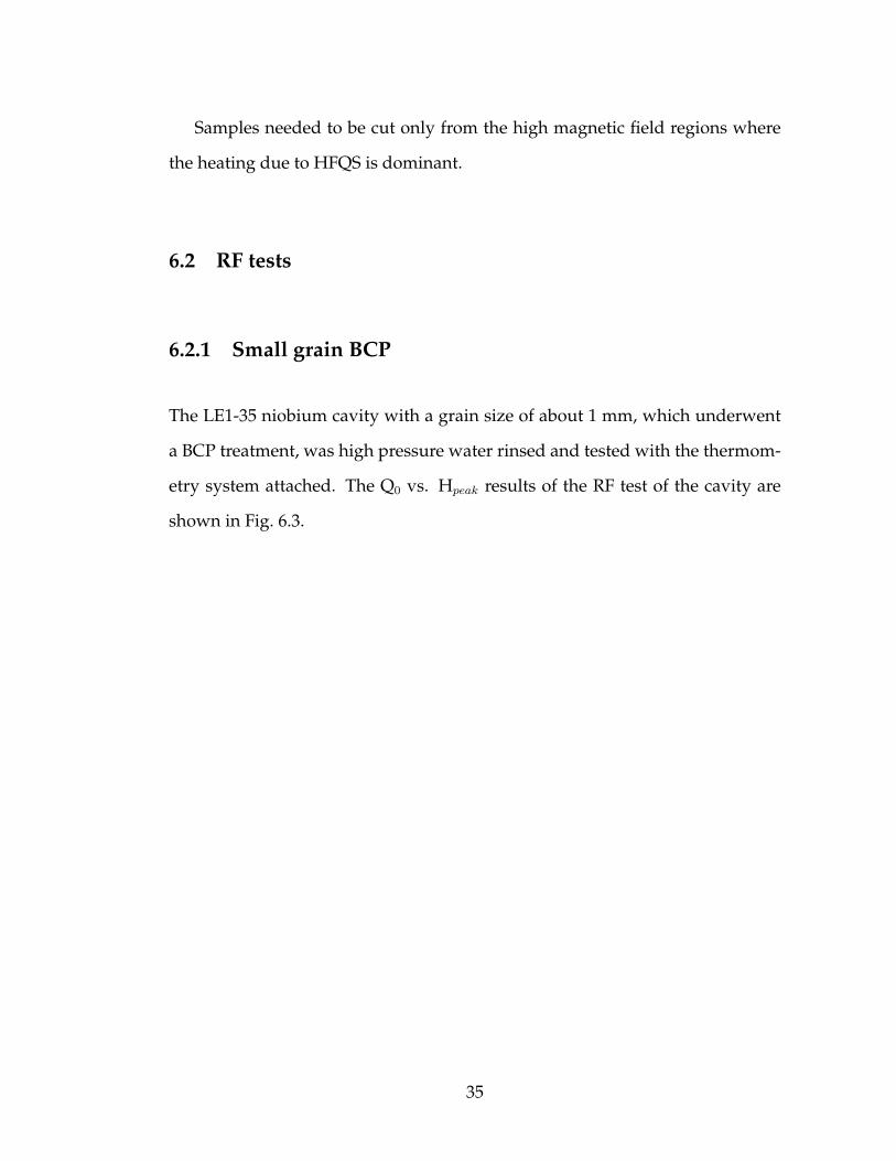
6 RF cavity tests and dissection 326.1 Introduction . . . . . . . . . . . . . . . . . . . . . . . . . . . . . . . 326.2 RF tests . . . . . . . . . . . . . . . . . . . . . . . . . . . . . . . . . . 35
6.2.1 Small grain BCP . . . . . . . . . . . . . . . . . . . . . . . . . 356.2.2 Large grain BCP . . . . . . . . . . . . . . . . . . . . . . . . 396.2.3 Small grain EP . . . . . . . . . . . . . . . . . . . . . . . . . 436.2.4 Small grain EP defects . . . . . . . . . . . . . . . . . . . . . 47
vii
7 Optical profilometry studies 507.1 Introduction . . . . . . . . . . . . . . . . . . . . . . . . . . . . . . . 507.2 Experimental data . . . . . . . . . . . . . . . . . . . . . . . . . . . . 517.3 Conclusion . . . . . . . . . . . . . . . . . . . . . . . . . . . . . . . . 53
8 XPS Studies 548.1 Introduction . . . . . . . . . . . . . . . . . . . . . . . . . . . . . . . 548.2 Small grain BCP cavity samples . . . . . . . . . . . . . . . . . . . . 58
8.2.1 Baking of the nitrogen-containing samples . . . . . . . . . 638.2.2 Angle-resolved XPS studies . . . . . . . . . . . . . . . . . . 64
8.3 Large grain BCP cavity samples . . . . . . . . . . . . . . . . . . . . 688.4 Small grain EP cavity samples . . . . . . . . . . . . . . . . . . . . . 728.5 Discussion . . . . . . . . . . . . . . . . . . . . . . . . . . . . . . . . 76
9 EBSD Studies on Cavity Samples 789.1 Introduction . . . . . . . . . . . . . . . . . . . . . . . . . . . . . . . 78
9.1.1 Dislocations . . . . . . . . . . . . . . . . . . . . . . . . . . . 799.2 Electron back-scattered diffraction . . . . . . . . . . . . . . . . . . 81
9.2.1 Local misorientation . . . . . . . . . . . . . . . . . . . . . . 839.2.2 Geometrically necessary dislocation content . . . . . . . . 859.2.3 Equivalence of LM and GND density characterizations . . 86
9.3 Crystalline orientation role in HFQS heating patterns . . . . . . . 889.4 Difference between hot and cold samples . . . . . . . . . . . . . . 899.5 Baking effect on cavity samples . . . . . . . . . . . . . . . . . . . . 95
10 Possible mechanisms for the HFQS and the mild baking effect 10110.1 Introduction . . . . . . . . . . . . . . . . . . . . . . . . . . . . . . . 10110.2 Bean-Livingston surface barrier . . . . . . . . . . . . . . . . . . . . 10210.3 Dislocation-based model for the HFQS . . . . . . . . . . . . . . . . 10410.4 Baking effect due to dislocation climb . . . . . . . . . . . . . . . . 113
11 Summary 116
A Positron annihilation studies 118
Bibliography 123
viii
LIST OF TABLES
2.1 Critical fields and temperature for high purity niobium (RRR =2000) from [23]. . . . . . . . . . . . . . . . . . . . . . . . . . . . . . 14
ix
LIST OF FIGURES
2.1 Electric and magnetic fields distribution on the cavity walls forthe elliptical MARK III shape (reproduced from [28]. . . . . . . . 6
2.2 Typical magnetization curves for type I and II superconductors. . 8
3.1 Typical Q0 vs. Epeak curve for SRF niobium cavities limited bythe high field Q-slope. . . . . . . . . . . . . . . . . . . . . . . . . . 18
4.1 Schematic of the grain boundary edge becoming normal con-ducting (left) and the corresponding fit to the Q0 vs. Eacc for theniobium cavity from [14]. . . . . . . . . . . . . . . . . . . . . . . . 21
4.2 Schematic of the interstitial oxygen distribution before and afterbaking within the weak superconducting layer model from [6]. . 23
4.3 Tunneling conductance curves for unbaked (top) and baked (bot-tom) niobium samples from [19]. . . . . . . . . . . . . . . . . . . . 25
5.1 SEM images of the EP (left) and BCP (right) finish from [16]. . . . 30
6.1 Schematic of the RF setup used for cavity testing (from [9]). . . . 336.2 The picture of the cavity, which had hot and cold areas cut out
for analysis. Arrow indicates one of the samples. . . . . . . . . . 346.3 LE1-35 cavity quality factor Q0 versus the peak magnetic field
Hpeak. The red square indicates the point, which corresponds tothe temperature map used for dissection. . . . . . . . . . . . . . . 36
6.4 The temperature map of the LE1-35 cavity obtained at the peakmagnetic field Hpeak = 120 mT. . . . . . . . . . . . . . . . . . . . . 37
6.5 Typical ∆T vs. Hpeak curves for LE1-35 small grain BCP cavityhot and cold samples. . . . . . . . . . . . . . . . . . . . . . . . . . 38
6.6 The interpolated contour plot of the LE1-35 temperature map atHpeak=120 mT. White circles indicate the cold regions, and redcircles - hot regions. . . . . . . . . . . . . . . . . . . . . . . . . . . 39
6.7 LE1-37 cavity quality factor Q0 versus the peak magnetic fieldHpeak. The red square indicates the point, which corresponds tothe temperature map used for dissection. . . . . . . . . . . . . . . 40
6.8 The temperature map of the LE1-37 large grain BCP cavity atHpeak=130 mT. Areas, which were selected for dissection: whitecircles - cold regions, red circles - hot regions. . . . . . . . . . . . 41
6.9 Typical ∆T vs. Hpeak curves for LE1-37 small grain BCP cavityhot and cold samples. . . . . . . . . . . . . . . . . . . . . . . . . . 42
6.10 LE1-35 cavity quality factor Q0 versus the peak magnetic fieldHpeak. The red square indicates the point, which corresponds tothe temperature map used for dissection. . . . . . . . . . . . . . . 44
x
6.11 The temperature map of the LE1-HOR small grain EP cavity atHpeak=120 mT. Areas, which were selected for dissection: whitecircles - cold regions, red circles - hot regions. . . . . . . . . . . . 45
6.12 Typical ∆T vs. Hpeak curves for LE1-HOR small grain EP cavityhot and cold samples. . . . . . . . . . . . . . . . . . . . . . . . . . 46
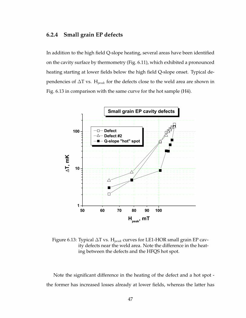
6.13 Typical ∆T vs. Hpeak curves for LE1-HOR small grain EP cavitydefects near the weld area. Note the difference in the heatingbetween the defects and the HFQS hot spot. . . . . . . . . . . . . 47
6.14 Secondary electrons images of the pit identified as a possiblecause of heating in the “defect” area of the small grain EP cavity. 48
6.15 Backscattered electrons images of the pit identified as a possiblecause of heating in the “defect” area of the small grain EP cavity. 49
7.1 Optical profilometer 3-D images (850 µm × 640 µm) of the hot(left) and cold (right) samples of the LE1-35 small grain BCP cavity. 51
7.2 Histograms of the step height distributions for the LE1-35 smallgrain BCP cavity hot and cold samples. . . . . . . . . . . . . . . . 52
7.3 Histograms of the step height distributions for the LE1-HORsmall grain EP cavity hot and cold samples. . . . . . . . . . . . . 53
8.1 Schematic of the niobium surface after typical cavity preparationsteps has been performed. . . . . . . . . . . . . . . . . . . . . . . . 54
8.2 Schematic of the typical lab XPS system. . . . . . . . . . . . . . . 568.3 Schematic of the photoelectric effect caused by the impinging X-
rays in the XPS setup. The resulting photoelectron comes fromthe 1s shell in this example. . . . . . . . . . . . . . . . . . . . . . . 56
8.4 XPS survey for the LE1-35 hot sample. Notice a strong N 1s peakindicating the presence of nitrogen in the first 7 nm of the sample. 59
8.5 XPS survey for the LE1-35 cold sample. Notice the absence of aN 1s peak. . . . . . . . . . . . . . . . . . . . . . . . . . . . . . . . . 60
8.6 XPS Nb 3d peak for the LE1-35 large grain BCP cavity hot andcold samples. . . . . . . . . . . . . . . . . . . . . . . . . . . . . . . 61
8.7 XPS spectra for the LE1-35 hot and cold samples obtained usingthe synchrotron X-rays of 2139 eV. Left panel shows the Nb 3dspectra, and the right panel shows the high resolution surveysaround the N 1s peak. Measurements by J. Woicik (NSLS). . . . . 62
8.8 XPS surveys for the hot, cold, and baked hot samples of the LE1-35 small grain BCP cavity. Notice the disappearance of the nitro-gen signal after 110C baking. . . . . . . . . . . . . . . . . . . . . 63
8.9 N 1s XPS peak for the hot, cold, and baked hot samples of theLE1-35 small grain BCP cavity. Notice the disappearance of thenitrogen signal after 110C baking. . . . . . . . . . . . . . . . . . . 64
8.10 Schematic of the typical ARXPS setup. . . . . . . . . . . . . . . . 65
xi
8.11 ARXPS depth profile of the nitrogen atomic concentration in theLE1-35 small grain BCP cavity samples. . . . . . . . . . . . . . . . 66
8.12 ARXPS depth profile of the carbon atomic concentration in theLE1-35 small grain BCP cavity samples. . . . . . . . . . . . . . . . 67
8.13 XPS survey for the LE1-37 large grain BCP cavity hot sample. . . 688.14 XPS survey for the LE1-37 large grain BCP cavity cold sample. . 698.15 XPS Nb 3d peak for the LE1-37 large grain BCP cavity hot sample. 708.16 XPS Nb 3d peak for the LE1-37 large grain BCP cavity cold sample. 708.17 XPS valence band spectrum for the LE1-37 large grain BCP cavity
hot sample. . . . . . . . . . . . . . . . . . . . . . . . . . . . . . . . 718.18 XPS valence band spectrum for the LE1-37 large grain BCP cavity
cold sample. . . . . . . . . . . . . . . . . . . . . . . . . . . . . . . . 728.19 XPS survey for the LE1-HOR small grain EP cavity hot sample. . 738.20 XPS survey for the LE1-HOR small grain EP cavity cold sample. 738.21 XPS Nb 3d peak for the LE1-HOR small grain EP cavity hot sample. 748.22 XPS Nb 3d peak for the LE1-HOR small grain EP cavity cold
sample. . . . . . . . . . . . . . . . . . . . . . . . . . . . . . . . . . 748.23 XPS valence band spectrum for the LE1-HOR small grain EP cav-
ity hot sample. . . . . . . . . . . . . . . . . . . . . . . . . . . . . . 758.24 XPS valence band spectrum for the LE1-HOR small grain EP cav-
ity cold sample. . . . . . . . . . . . . . . . . . . . . . . . . . . . . . 76
9.1 (a) Cutting plane determines a dislocation line vector ~t; (b) dis-placement of the lattice for edge dislocations: ~b ⊥ ~t; (c) ~b ‖ ~t forscrew dislocations. . . . . . . . . . . . . . . . . . . . . . . . . . . . 79
9.2 3D-view of an ideal edge dislocation. . . . . . . . . . . . . . . . . 809.3 Schematic of a typical EBSD system setup (left) and the for-
mation of diffraction pattern on the acquisition screen (Kikuchibands). . . . . . . . . . . . . . . . . . . . . . . . . . . . . . . . . . . 82
9.4 Example of an EBSD crystal orientation map (left) and a localmisorientation map obtained from it (right) for the fine grainBCP niobium sample. Covered area is 150x150 µm. Color leg-end for orientations is shown on the left and the misorientationcolor coding (in degrees) on the right. . . . . . . . . . . . . . . . . 84
9.5 Local misorientation distributions for hot and cold samples ofLE1-37 large grain BCP cavity (top graph). Compare with thedislocation density distribution (bottom graph) for the samesamples. . . . . . . . . . . . . . . . . . . . . . . . . . . . . . . . . . 87
9.6 Inverse pole figures showing random spread in grain orienta-tions for hot (left panel) and cold (right panel) spots in LE1-35small grain BCP cavity. Data for all measured samples is in-cluded. Notice lack of 〈101〉 orientations in both cases. . . . . . . 89
xii
9.7 Local misorientation maps for H6 hot spot (left) and C11 coldspot (right) of a LE1-37 large grain BCP cavity. Map dimensionsin both cases are 400x400 µm. Notice a drastically different mi-crostructure. . . . . . . . . . . . . . . . . . . . . . . . . . . . . . . . 91
9.8 Local misorientation distributions averaged over all hot and coldspots for LE1-37 large grain BCP cavity. . . . . . . . . . . . . . . . 92
9.9 Local misorientation distributions for hot and cold spots for LE1-35 small grain BCP cavity. . . . . . . . . . . . . . . . . . . . . . . . 93
9.10 Local misorientation distributions averaged over all hot and coldspots for LE1-HOR small grain EP cavity. . . . . . . . . . . . . . . 94
9.11 Local misorientation distributions for H6 hot spot of a LE1-37large grain BCP cavity before and after baking at 110C for 48hours. . . . . . . . . . . . . . . . . . . . . . . . . . . . . . . . . . . 96
9.12 Local misorientation distributions for the H1 hot spot of a LE1-HOR small grain EP cavity before and after baking at 120C for40 hours. . . . . . . . . . . . . . . . . . . . . . . . . . . . . . . . . . 97
9.13 Local misorientation distributions for the C3 cold spot of a LE1-HOR small grain EP cavity before and after baking at 120C for24 hours. . . . . . . . . . . . . . . . . . . . . . . . . . . . . . . . . . 98
9.14 Local misorientation distributions for the H4 hot spot of a LE1-35 small grain BCP cavity before and after baking at 120C for 63hours. . . . . . . . . . . . . . . . . . . . . . . . . . . . . . . . . . . 99
10.1 Dependence of the fluxoid line energy on distance from the sur-face for different applied magnetic fields (reproduced from [4]). . 103
10.2 Effect of the subsequent room temperature annealing on thelead-8.23 wt.% indium alloy. A–as-cold swaged, B–annealed 30min, C–1 day, D–18 days, E–46 days (reproduced from [29]). . . . 104
10.3 Schematic of the single fluxoid within the London penetrationdepth of the niobium surface with the forces acting on it in theRabinowitz’s model [39, 38]. . . . . . . . . . . . . . . . . . . . . . 107
10.4 TEM micrographs of the dislocation cell structure in niobiumwires (reproduced from [43]). . . . . . . . . . . . . . . . . . . . . . 112
10.5 Schematic of the edge dislocation climb through vacancy diffusion.114
A.1 S-parameter vs. depth for a single grain BCP sample. The peakin S-parameter close to the surface appeared after vacuum failureand was removed by a 160C in situ baking for 2 days. . . . . . . 119
A.2 S-parameter at a fixed positron energy E = 2 keV vs. baking tem-perature for a single grain BCP sample. Note the onset of theS-parameter decrease at T = 80C. . . . . . . . . . . . . . . . . . . 121
xiii

A.3 S-parameter vs. positron energy for a single grain BCP sample.The peak in S-parameter appeared after vacuum failure and wasremoved by a ramp annealing. Air exposure did not bring thepeak back. . . . . . . . . . . . . . . . . . . . . . . . . . . . . . . . . 122
xiv
CHAPTER 1
INTRODUCTION
Superconducting radio frequency (RF) cavities have become the prime technol-
ogy choice for current and future particle accelerators such as CESR, CEBAF,
XFEL, ERL, ILC etc. The main advantage of the superconducting niobium cav-
ities over the previously standard normal conducting copper cavities is the ex-
tremely low dissipated power due to the small RF losses in the superconduct-
ing state. This results in an efficient transfer of RF power to the particle beam
power. Still, the advantage in losses comes with the cost of the power for cav-
ity refrigeration, which is needed to keep superconducting cavities at typical
operating temperatures of 1.5-4.2 K depending on the RF frequency for the par-
ticular application. Nevertheless the total AC power needed to provide a given
accelerating gradient is less in the case of the superconducting cavities than in
the case of normal conducting ones for CW and high duty factor operation.
Accelerating gradients up to the record value of 59 MV/m have been demon-
strated in niobium single cell cavities. In the case of multicell cavities intended
for use in future accelerators such as ILC, the achieved gradients are lower.
The specification for ILC is currently to have an average qualifying gradient
of 35 MV/m in 1.3 GHz 9-cell cavities, which is not yet achieved with a high
enough consistency.
Even though record-high gradients are achieved in single cell cavities, there
are gaps in the understanding of the physics behind the various effects that de-
pend on surface condition and variations in cavity performance. Most of the
recently adopted preparation steps are not well understood and were empiri-
cally found to improve the high field surface resistance, or the quench field. For
1

example, electropolishing, which has become a standard step in cavity prepara-
tion (instead of a formerly routine buffered chemical polishing), followed by a
100-120C in situ annealing of the cavity for 1-2 days allows small grain cavities
to consistently achieve a high quality factor up to the highest accelerating gradi-
ent. Whereas small grain cavities, which undergo a buffered chemical polishing
and baking, are often limited by the unexplained high field degradation of the
quality factor, one of the main topics of this thesis. The benefits of mild baking
are not yet understood.
Historically, as soon as the physics was understood behind each of the lim-
itations encountered in the quest for higher accelerating gradients, a new treat-
ment recipe(s) was invented that significantly improved consistently achieved
gradients and optimized the time and cost for the cavity preparation. Currently,
the high field behavior of RF cavities (high field Q-slope) and its dependence on
the surface conditions is a major puzzle to be solved.
The main topic of this thesis work is to try to understand how the detail
nature of the RF surface translates into the high field surface resistance.
This thesis is organized as follows.
In Chapter 2 an overview of the RF cavities is given, and properties of nio-
bium in the superconducting state are discussed.
In Chapter 3, known sources of dissipation in cavities are presented and the
little understood Q-slopes at low, medium and high fields are introduced.
In Chapter 4, several recently proposed models for the high field Q-slope are
reviewed, and the problems with each of them are discussed.
2
In Chapter 5, a brief overview is given of cavity preparation steps, which
will be involved in the discussion of the thesis results.
In Chapter 6, results of the RF tests on the cavities used in this thesis work
are reported.
Chapter 7 presents the results of the optical profilometry analysis of the
roughness on the samples dissected from the cavities.
Chapter 8 reports on XPS investigations of the niobium oxide structure of
the cavity samples.
Chapter 9 presents the results of the EBSD analysis of the crystalline mi-
crostructure of the samples. A method of analysis based on the local misorien-
tation is applied to analyze the difference in the dislocation content between the
samples and the effect of the mild baking.
Based on the experimental results a model is presented in Chapter 10 for the
HFQS and the mechanism behind the mild baking effect.
Summary of the thesis work is given in Chapter 11.
In Appendix A, preliminary results of the positron annihilation studies of
the vacancy concentration in niobium samples are presented.
3
CHAPTER 2
SUPERCONDUCTING RF CAVITIES
2.1 Cavity Fundamentals
Niobium superconducting cavities are radio frequency (RF) resonators, which
provide the electric field to accelerate a particle beam. The accelerating gradient
is defined as an energy gain per unit length:
Eacc =Vacc
d(2.1)
where d is the length of the cavity, and Vacc is the accelerating voltage defined as
Vacc =
∣∣∣∣1
e×maximum energy gain possible during transit
∣∣∣∣ (2.2)
If we consider axis z to be aligned with the cavity symmetry axis, and the
cavity resonates at the mode of angular frequency ω, then we have for Vacc:
Vacc =
∣∣∣∣∫ d
0
Ez(z)eiωz
c dz
∣∣∣∣ (2.3)
The RF field in the cavity leads to the dissipation in the cavity walls due to
the non-zero microwave resistance of superconducting niobium, which will be
discussed in the following chapter. The non-zero dissipation is characterized by
the surface resistance Rs, and the magnitude of the magnetic field at the cavity
surface. The power dissipated per unit area of the wall is:
dPdiss
ds=
1
2Rs |H|2 (2.4)
where H is the local magnetic field amplitude. Hence, the total dissipated power
Pdiss is given by an integral over the interior cavity wall:
Pdiss =1
2Rs
∫
S
|H|2 ds (2.5)
4
In practice, it is more convenient to characterize cavity losses using a cavity
quality factor Q0, which is defined as:
Q0 =ωU
Pdiss
(2.6)
where ω is the angular frequency of the operating field mode, and U is the stored
energy of the electromagnetic field in the cavity, which can be calculated from
the magnetic field amplitude:
U =1
2µ0
∫
V
|H|2 dV (2.7)
For the cavity quality factor Q0 we then obtain:
Q0 =ω0µ0
∫V|H|2 dV
Rs
∫S|H|2 ds
=G
Rs
(2.8)
where
G =ω0µ0
∫V|H|2 dV∫
S|H|2 ds
(2.9)
is the geometry factor, which only depends on the cavity shape and the distribu-
tion of the electromagnetic field in the accelerating mode.
The distribution of the electromagnetic field in the cavity is governed by
Maxwell’s equations, which reduce to the wave equations for the case of the
fields in the cavity: (∇2 − 1
c2
∂2
∂t2
)(EH
)= 0 (2.10)
If we assume that niobium surface behaves as a perfect conductor, then the
boundary conditions, which have to be satisfied at the cavity wall are:
n× E = 0, n ·H = 0 (2.11)
Two families of solutions exist to the Eq. (2.10), which are denoted as trans-
verse magnetic (TM) modes and transverse electric (TE) modes. For TM modes the
5
magnetic field is everywhere transverse to the z-axis, whereas the electric field
is transverse to the z-axis for TE modes. For the purpose of particle acceleration
only TM modes are useful, since TE modes do not have a longitudinal electric
field on the beam axis. Typically, SRF cavities are operated in the TM010 mode,
which has the lowest eigenfrequency among the TM modes.
The analytical solution for the cavity with the input coupler port and
other symmetry-breaking parts does not exist, so usually computer-based field
solvers (i.e. SLANS, Microwave Studio) are used to find the distribution of the
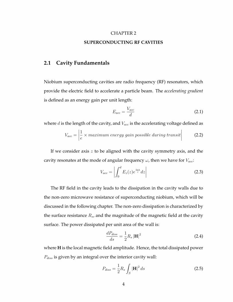
fields inside the cavity. For Mark III shape elliptical cavities used in this the-
sis work, the distribution of the electric and magnetic fields on the walls of the
cavity is shown in Fig. 2.1.
Figure 2.1: Electric and magnetic fields distribution on the cavity walls forthe elliptical MARK III shape (reproduced from [28].
6

The geometry factor, which is provided by the field solvers as well, is G =
273 Ω and the ratios of the highest surface electric and magnetic fields to the
accelerating gradient Eacc are:
Epeak
Eacc
∼= 1.83
Hpeak
Eacc
∼= 44.98Oe
MV/m
(2.12)
2.2 Superconductivity
Superconductivity was discovered in 1911 by H. Kamerlingh-Onnes in mercury,
lead and tin, when he observed a complete disappearance of the electrical resis-
tance below the material-specific critical temperature Tc. A complete theoretical
understanding of classic superconductors was not achieved until the BCS the-
ory was formulated in 1950s. Up to now many elements and compounds have
been found to possess superconducting properties. Among the superconduct-
ing elements niobium has the highest critical temperature and relatively high
critical fields, which motivates its choice as a material for superconducting RF
cavities.
2.2.1 Properties of superconductors
Superconductors have two main characteristic properties. The first one is an
absence of any measurable resistance to DC electric currents below the criti-
cal temperature Tc. The second one is perfect diamagnetism, which is the ex-
pulsion of any external magnetic field from the interior of the superconductor
up to the critical field Bc – called a Meissner-Ochshenfeld effect. For type I
7
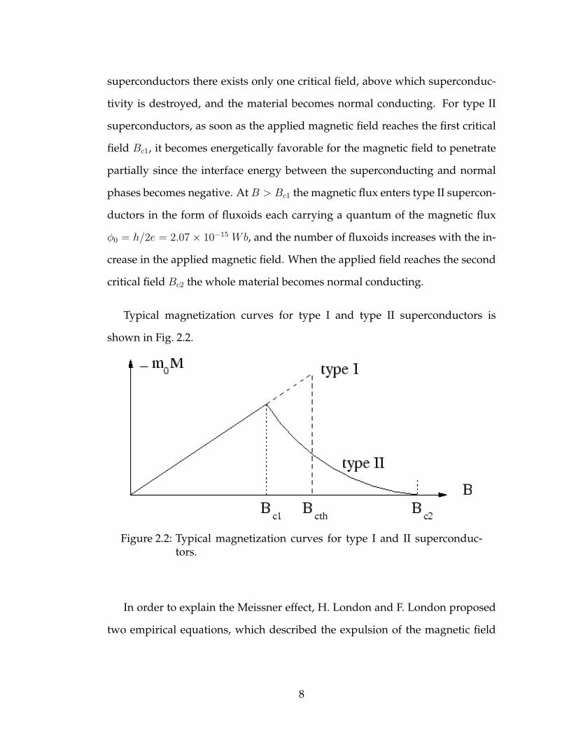
superconductors there exists only one critical field, above which superconduc-
tivity is destroyed, and the material becomes normal conducting. For type II
superconductors, as soon as the applied magnetic field reaches the first critical
field Bc1, it becomes energetically favorable for the magnetic field to penetrate
partially since the interface energy between the superconducting and normal
phases becomes negative. At B > Bc1 the magnetic flux enters type II supercon-
ductors in the form of fluxoids each carrying a quantum of the magnetic flux
φ0 = h/2e = 2.07× 10⁻¹⁵ Wb, and the number of fluxoids increases with the in-
crease in the applied magnetic field. When the applied field reaches the second
critical field Bc2 the whole material becomes normal conducting.
Typical magnetization curves for type I and type II superconductors is
shown in Fig. 2.2.
Figure 2.2: Typical magnetization curves for type I and II superconduc-tors.
In order to explain the Meissner effect, H. London and F. London proposed
two empirical equations, which described the expulsion of the magnetic field
8
from the bulk of a superconductor:
∂J∂t
=nse
2
mE (2.13)
m
nse2∇× J = −B (2.14)
Using London equations 2.13-2.14 and Maxwell’s equations we obtain for the
static field distribution at the half-space filled with superconductor:
B(z) = B0e− z
λL , J(z) = J0e− z
λL (2.15)
so that the magnetic field and the shielding current density have a finite pene-
tration depth, which is characterized by a constant
λL =
√m
µ0nse2(2.16)
named a London penetration depth. For a very high purity niobium (RRR =
2000), the London penetration depth was measured to be λL ≈ 40 nm [23]. The
temperature dependence of the penetration depth is given by:
λL(T ) =λL(0)√
1−(
TTc
)4(2.17)
An extremely successful theory of superconductivity was developed by
Bardeen, Cooper and Schrieffer in 1957 [2]. The fundamental effect underly-
ing the superconductivity is the “condensation” of electrons within kBTc ≈ hωD
of the Fermi surface into pairs due to the effective attractive interaction caused
by lattice vibrations (phonons). The resulting Cooper pairs can be considered as
single particles carrying a charge of 2e and a mass of 2m with the pairing energy
of 2∆. A new density of states near the Fermi surface exhibits an energy gap ∆,
which is the absence of any energy levels within 2∆ from the Fermi surface εF .
9

The BCS theory predicts the following relation between the superconducting
gap at T = 0 K and the critical temperature:
2∆(0) = 2× (1.76kBTc) = 3.12 meV (2.18)
The actual size of the gap depends on the strength of electron-phonon inter-
action, and for niobium it was found to be ∆(0)/kBTc = 1.9. A characteristic
length scale for the Cooper pair, also known as a coherence length, can be found
from Heisenberg’s uncertainty principle, and in terms of the Fermi velocity vF
is given by:
ξ0 =hvF
kBTc
=hvF
∆(2.19)
For niobium ξ0 ≈ 39 nm.
A Ginzburg-Landau parameter is defined as a ratio of London penetration
depth and a coherence length:
κ =λL
ξ0
(2.20)
and the value of κ determines if the superconductor is type I or type II. For type
I: κ < 1√2, and for type II: κ > 1√
2. For niobium we have κ ≈ 1, and it is a weak
type II superconductor.
A zero DC resistance in the superconducting state can be understood based
on the two-fluid model. One fluid is a superfluid of electrons condensed into
Cooper pairs, and the other fluid is a normal fluid of free electrons. At T = 0 K
all of the electrons are paired, but at a finite temperature T < Tc a fraction of
unpaired electrons is given by the Boltzmann factor exp(−∆/kbT ).
Cooper pairs move through the lattice without dissipation if the thermal en-
ergy of phonons is less than the superconducting gap 2∆, i.e. T < Tc. Thus the
supercurrent flows with zero DC electric resistance. Normal and superconduct-
10

ing current components are effectively in parallel, but since the supercurrent ex-
periences no resistance, the total current is carried exclusively by Cooper pairs,
whereas normal electrons are shielded from the electric field, and hence there is
no normal current, which would produce dissipation.
In the case of RF currents though, the resistance of superconductors is not
zero. A finite resistance arises due to the inertial mass of Cooper pairs. When the
superconductor is exposed to the time-varying electric field, the Cooper pairs
(superfluid) are unable to completely shield the normal fluid. Time-varying
magnetic field in the penetration depth induces a time-varying electric field,
which acts on the normal electrons and causes dissipation. From Faraday’s law
an induced electric field is proportional to the magnetic field rate of change:
Eind ∝ dH
dt∝ ωH (2.21)
and the resulting normal current density is
jn ∝ nnE ∝ nnωH (2.22)
where nn is the number of normal electrons, nn ∝ exp(− ∆
kBT
). The dissipated
power produced by RF currents is then:
Pdiss ∝ jnEind ∝ nnω2H2 (2.23)
Using Eq. (2.4) we finally obtain:
Rs ∝ nnω2 ∝ ω2exp
(− ∆
kbT
)(2.24)
The exact expression for the surface resistance involves several material pa-
rameters, but a good practical approximation for T < Tc/2 and for frequencies
much smaller than 2∆/h ≈ 1012 Hz is
RBCS = 2× 10⁻⁴ 1
T
(f
1.5
)2
exp
(−17.67
T
)(2.25)
11
where f is the RF frequency in GHz.
2.2.2 Critical fields
A thermodynamic critical field Hc is defined by the magnetic energy density
needed to overcome the reduction in the free energy fn(T ) − fs(T ) due to the
condensation into the superconducting state:
H2c (T )
8π= fn(T )− fs(T ) (2.26)
It is approximated very well by a parabolic law:
Hc(T ) ≈ Hc(0)
[1−
(T
Tc
)2]
(2.27)
The thermodynamic critical field is a measurable property of type I super-
conductors, but for type II superconductors there is no physical phenomenon,
which takes place at that field. For type II superconductors the surface energy of
the normal-superconducting interface becomes negative as soon as the applied
magnetic field reaches the lower critical field Hc1. A negative surface energy
makes it energetically favorable to have a mixed state with the partial penetra-
tion of the magnetic flux in the form of fluxoids each carrying a quantum of
the magnetic flux φ0. With further increase in the applied field, the number of
fluxoids penetrating the material increases, until their normal conducting cores
start to overlap, which happens at the higher critical field Hc2, and the super-
conductivity is destroyed in the bulk of the superconductor. For measurements
with very high purity niobium (RRR = 2000), critical fields were reported in [23]:
Hc1 = 1800 Gauss,Hc2 = 3900 Gauss.
12

The Ginzburg-Landau (G-L) theory [24], although applicable for tempera-
tures T not much below Tc, allows an estimate of both Hc1 and Hc2 in some
limits. For the higher critical field Hc2 it gives:
Hc2 =√
2κHc (2.28)
and for the lower critical field in the limit κ À 1 (which is not a good approxi-
mation for niobium):
Hc1 =logκ + 0.081
κ√
2(2.29)
The calculations of the bulk critical fields within the G-L theory neglect finite
dimensions, and for real superconductors, surface effects should be considered
as well. Saint-James and de Gennes [42] showed that superconductivity can be
sustained at a metal-insulator interface in a parallel field Hc3, higher by a factor
of 1.695 than Hc2. The detailed analysis of the boundary conditions in the G-L
theory shows that:
Hc3 = 1.695Hc2 = 1.695(√
2κHc) (2.30)
Furthermore, in the absence of nucleation centers at the surface of super-
conductors, “superheated” superconducting state may persist metastably for
H > Hc up to the superheating critical field Hsh. A superheating field can be
calculated in various limits using the G-L theory:
Hsh = 0.75Hc for κ >> 1
Hsh = 1.2Hc for κ ≈ 1
Hsh =Hc√
κfor κ << 1
(2.31)
Practically, for niobium cavities there is much discussion at this point, about
which of the critical fields is the ultimate limit. RF surface magnetic fields in
13

Table 2.1: Critical fields and temperature for high purity niobium (RRR =2000) from [23].
Property Measured value
Tc 9.29 K
Hc 2061 Gauss
Hc1 1800 Gauss
Hc2 3900 Gauss
excess of Hc1 and Hc have been successfully demonstrated recently in single
cell niobium cavities [18, 17]. There is also some evidence that Hc1 might be
the practical limiting field due to a strong dissipation caused by the penetrating
fluxoids as will be discussed in Ch. 10.
14

CHAPTER 3
LOSSES IN SUPERCONDUCTING NIOBIUM CAVITIES
3.1 Residual resistance
The surface resistance of niobium as calculated from the cavity quality factor is
in practice higher than the corresponding BCS surface resistance and the total
surface resistance can typically be written in the form:
Rs = RBCS(T ) + Rres (3.1)
where RBCS(T) is the temperature-dependent BCS surface resistance, and Rres
is the temperature-independent residual resistance. There are several possible
sources of the residual resistance, which are understood, such as trapped mag-
netic flux and niobium hydrides, but in the absence of these sources niobium
cavities still have a few nΩ of the residual resistance, the origin of which is not
clear, but possible sources could be absorbed gases etc. One should distinguish
between the fundamental losses, which are inherent to the cavity material, and
parasitic losses caused by different extrinsic phenomena discussed below.
3.2 Multipacting
The multipacting phenomenon in niobium cavities is a resonant process of the
incident power absorption by the electrons originating from the cavity walls.
Roughly speaking, if the electron emitted from the niobium surface by some
physical mechanism (i.e. cosmic rays, field emission, photoemission etc.) is ac-
celerated by the cavity electric field and upon colliding with the cavity surface
15
produces more than one secondary electron, then the the number of electrons
involved multiplies (hence the name). Secondary electrons are accelerated in
trajectories that return to the surface and upon impact produce more electrons.
The resulting avalanche current is limited only by the available RF power and
the space-charge effects, and hence it becomes impossible to raise the field in the
cavity beyond the multipacting barrier. In order for multipacting to be possible,
the secondary emission coefficient should be high enough, and the electron tra-
jectories in the cavity should satisfy certain resonant conditions. By selecting
the proper cavity shape it is possible to choose a design such that multipacting
is avoided. As soon as the physical mechanism was identified, the spherical and
elliptical cavity shapes emerged, which essentially eliminated the multipacting
problem, by making the accelerated electrons move towards the cavity equa-
tor where the electric field is zero and secondary electrons can not gain enough
energy to produce secondaries.
3.3 Field emission
Field emission is a well-known effect of the emission of electrons from the regions
at the surface where the applied electric field is high and electrons in niobium
can tunnel through the work function barrier. The theory of field emission was
developed by Fowler and Nordheim (FN) [22] and gives the following expres-
sion for the tunneling current density:
j =e2
8πh
E2
φt2(y)exp
−
8π√
2m (eφ)3v(y)
3heE
(3.2)
where e is the electron charge, m is the electron mass, h is a Planck’s constant,
φ is the work function in eV, and E is the instantaneous electric field in MV/m.
16
In practice, for niobium cavities the FN current density should be modified by
using βE instead of E, where β is the field enhancement factor that originates
from the electric field enhancement at sharp tips on the surface.
Areas of the cavity surface that have a higher β value or a reduced work
function will become field emission sites at lower electric fields. The nature of
field emitters was studied in detail in [28] and the general conclusion is that
most of the field emitters are either foreign particles or protrusions on the sur-
face such as scratches.
The natural way to overcome the field emission is to use the high pressure
ultrapure water rinsing (HPR) in order to remove the majority of the particle
contaminants from the cavity surface. If the field emitter is still present even
after the HPR, it is sometimes possible to eliminate it by high power processing
when the field emitter particle is heated up by a short pulse of a very high RF
power to the temperature of evaporation. In general, the field emission phe-
nomenon is well understood and can be overcome by cleanliness methods.
3.4 Q-slopes
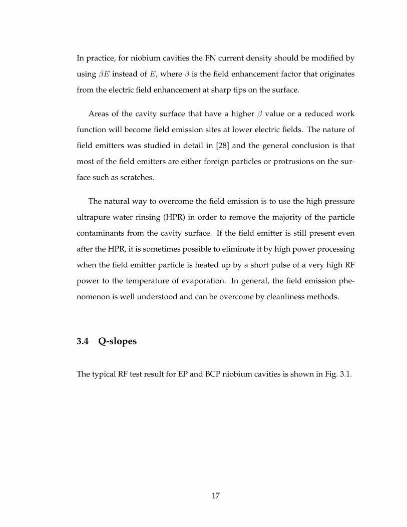
The typical RF test result for EP and BCP niobium cavities is shown in Fig. 3.1.
17

Figure 3.1: Typical Q0 vs. Epeak curve for SRF niobium cavities limited bythe high field Q-slope.
It is clearly observed that the dependence has three distinct regions, which
are respectively called low, medium and high field Q-slopes.
3.4.1 Low field Q-slope
Low Field Q-slope (LFQS) is a decrease in the cavity surface resistance with field
in the range of the Eacc below approximately 5 MV/m. The physical mechanism,
which underlies the effect, is not clear at this time although several mechanisms
are proposed, but since the LFQS does not represent any obstacles to the cavity
performance, it obtained relatively low attention as compared to the following
Q-slopes.
18

3.4.2 Medium field Q-slope
Medium Field Q-slope (MFQS) is a mild degradation of the cavity quality factor
with field until the quench or a high field Q-slope limitation is reached. Al-
though the full understanding of the effect has not been yet developed, there
is a strong theoretical indication that the MFQS is due to the positive feedback
between the surface heating and the BCS surface resistance [15].
3.4.3 High field Q-slope
The high field Q-slope is a general phenomenon in superconducting niobium
cavities, which arises in the absence of the parasitic losses discussed above (mul-
tipacting, field emission, hydrides) as soon as the peak magnetic field at the nio-
bium surface reaches about 100 mT. The manifestation of the HFQS is the sharp
increase in the surface resistance of niobium with the increased magnitude of
the applied magnetic field. This in turn translates into the degradation of the
cavity quality factor Q0, which limits the achievable accelerating gradient. The
HFQS is generic in the sense that BCP and EP cavities of all grain sizes exhibit
the same behavior if no further annealing was applied after the chemical treat-
ment. An empirical “cure” for the HFQS was found, which is an in situ baking
of the cavity at 100-120C in UHV for 12-48 hours depending on the grain size.
Although baking allows to consistently prepare high performance niobium cav-
ities, which do not have the HFQS, it is a time-consuming process (2 days), and
the understanding of the physics behind the HFQS and the mild baking effect
would possibly result in techniques leading to a substantial decrease in the cav-
ity preparation time, and possibly better performance.
19
CHAPTER 4
HIGH FIELD Q-SLOPE MODELS
4.1 Introduction
Several models have been proposed in the recent decade to account for the ob-
served high field Q-slope in niobium cavities including:
• Thermal Feedback [25]
• Interface Tunnel Exchange (ITE) model [27]
• Magnetic Field Enhancement (MFE) [14]
• Weak superconducting layer model [41]
• Modified oxygen pollution layer model [8]
• Magnetic impurities in the oxide [19]
In general, none of the theories agrees fully or satisfactorily with the experimen-
tal data, and some of them such as ITE and thermal feedback can already be
excluded, since HFQS was shown to be a magnetic field effect, and the thermal
feedback does not produce enough dissipation to account for the HFQS. Below
we briefly describe the models, which can still explain the high field Q-slope
at least partially, and present experimental facts that falsify them as a complete
story.
20
4.2 Magnetic Field Enhancement (MFE)
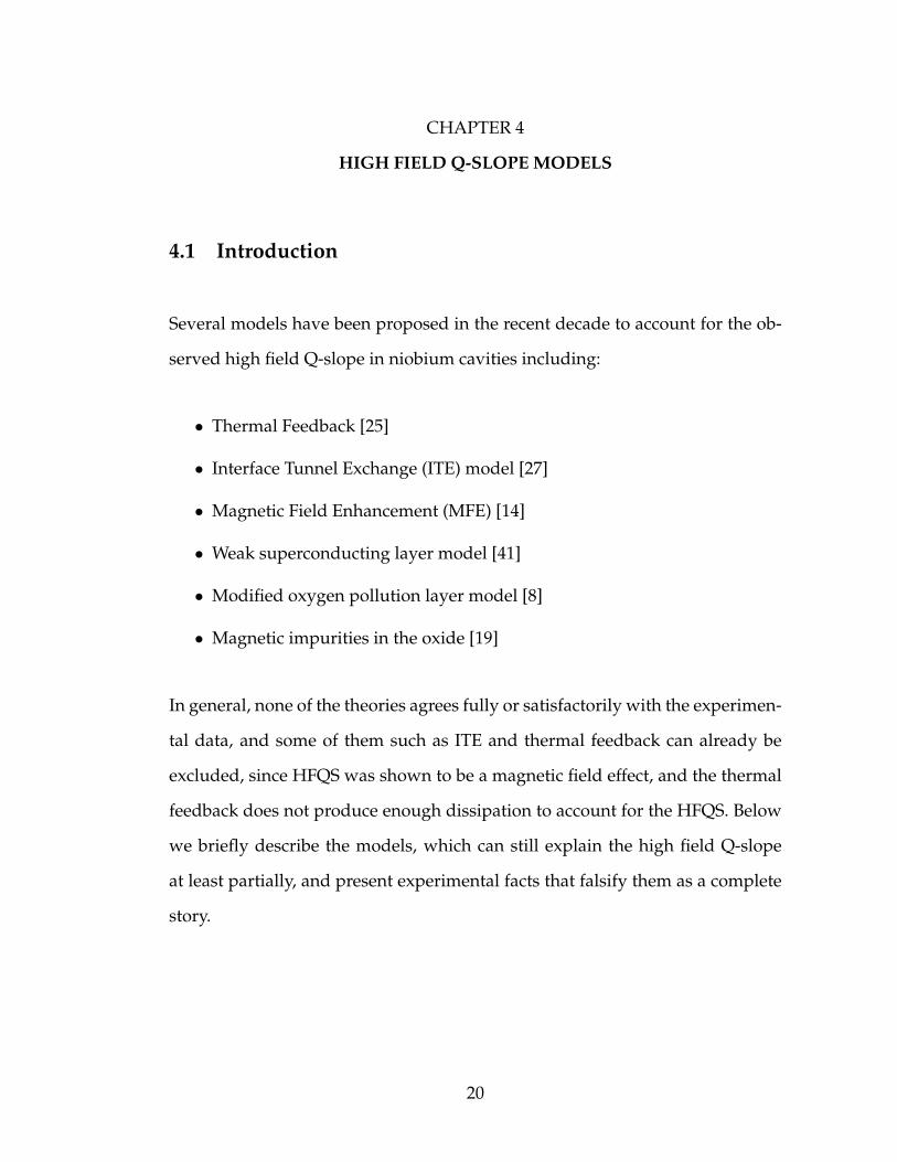
The MFE model presented in [14] attributes the HFQS to the enhancement of the
magnetic field at the sharp edges of the grain boundaries (see Fig. 4.1), which
are especially pronounced for the small grain BCP cavities. Similarly to the elec-
tric field enhancement at sharp tips, the magnetic field is enhanced at the grain
boundaries, and the enhancement factor can be as high as two as follows from
the finite element simulations. As soon as the local magnetic field reaches the
critical field, the area around the grain boundary edge becomes normal con-
ducting and the dissipation increases sharply.
Figure 4.1: Schematic of the grain boundary edge becoming normal con-ducting (left) and the corresponding fit to the Q0 vs. Eacc forthe niobium cavity from [14].
The MFE model gives a reasonable fit to the cavity data, but there are several
experimental results, which strongly oppose it. The obvious inconsistency is the
presence of the HFQS in single grain cavities with no grain boundaries. In ad-
dition, despite the significant difference in roughness between small grain BCP
and EP cavities, smoother EP cavities also show the HFQS - BCP and EP cavities
that were not baked, behave remarkably similar. Another major difficulty is that
21

the baking effect is not described by the model since the surface roughness does
not change due to baking.
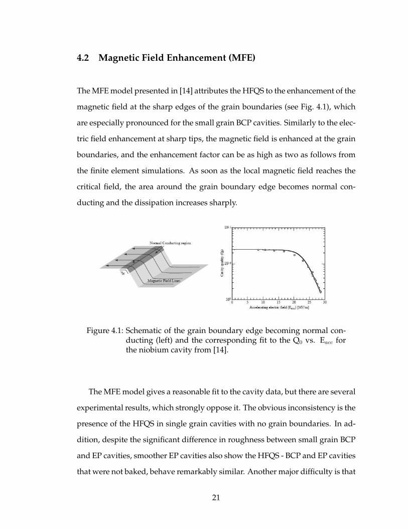
4.3 Weak superconducting layer
The essence of this model is the possible existence of the “weak” superconduct-
ing layer with depressed superconducting properties just underneath the oxide
layer on niobium. The degraded superconducting properties are attributed to
the high concentration of the interstitial oxygen, which is known to strongly
depress the niobium superconducting properties if present in concentrations of
several atomic percent. Thus the critical field in the “weak” layer is reached at
lower applied RF fields and the high field Q-slope emerges. Another basis for
this model is the low temperature baking effect. Common interstitial impurities
present in the cavity grade niobium are H, O, C and N. Since the low tempera-
ture baking at 100C was found to remove the high field Q-slope in EP cavities
of all grain sizes and large grain BCP cavities, it was suggested that the effect
might come from the diffusion of interstitials. At the temperatures of 100-120C
both N and C are believed to be not mobile enough due to their low bulk dif-
fusion coefficient, and H is mobile even at room temperature thus making any
change of its depth profile reversible. Oxygen, on the other hand, has an appro-
priate diffusion coefficient that can explain the change in the material within the
magnetic field penetration depth. For typical baking durations of 24-48 hours it
was calculated that oxygen diffusion length is about 20 nm, which is consistent
with the thickness of the baking-modified layer [9]. The schematic of the baking
effect on the high-concentration oxygen layer is shown in Fig. 4.2.
22
Figure 4.2: Schematic of the interstitial oxygen distribution before andafter baking within the weak superconducting layer modelfrom [6].
The major obstacle for this model to succeed is the lack of experimental evi-
dence for the high oxygen-content layer underneath the oxide. Recent XPS [12]
and SIMS [40] studies showed that this layer does not exist and the modifica-
tion of the oxide and the interstitial oxygen content during the mild baking is
reversed as soon as the cavity is exposed to the atmospheric air, which is in
contradiction to the cavity experiments that show an unchanged baking benefit
even after a year of air exposure. Other data not explained by this model is the
superiority of small grain EP cavities over small grain BCP cavities after baking,
since there is no reason to believe that the difference in roughness might affect
the oxygen diffusion during baking.
23
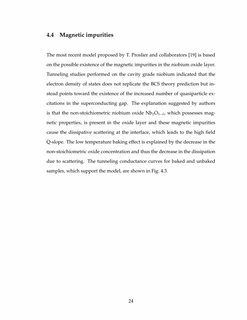
4.4 Magnetic impurities
The most recent model proposed by T. Proslier and collaborators [19] is based
on the possible existence of the magnetic impurities in the niobium oxide layer.
Tunneling studies performed on the cavity grade niobium indicated that the
electron density of states does not replicate the BCS theory prediction but in-
stead points toward the existence of the increased number of quasiparticle ex-
citations in the superconducting gap. The explanation suggested by authors
is that the non-stoichiometric niobium oxide Nb2O5−δ, which possesses mag-
netic properties, is present in the oxide layer and these magnetic impurities
cause the dissipative scattering at the interface, which leads to the high field
Q-slope. The low temperature baking effect is explained by the decrease in the
non-stoichiometric oxide concentration and thus the decrease in the dissipation
due to scattering. The tunneling conductance curves for baked and unbaked
samples, which support the model, are shown in Fig. 4.3.
24

Figure 4.3: Tunneling conductance curves for unbaked (top) and baked(bottom) niobium samples from [19].
We believe that this model contradicts several experimental facts as found
by cavity tests and surface studies. First, cavity experiments show that the high
field Q-slope is not restored by the hydrofluoric acid rinsing of the baked cavity
where the HFQS is healed. The effect of the HF treatment on niobium is the re-
moval of the remaining oxide layer, which is subsequently regrown after water
rinsing and air exposure. If the non-stoichiometric oxide inclusions were re-
moved by the baking, there is a good reason to believe that a new oxide should
again have similar magnetic impurities.
Furthermore, recent XPS studies [12] of the mild baking effect in UHV on
the niobium oxide structure show that the slight changes caused by baking are
completely reversible by the subsequent atmospheric air exposure. But cavity
experiments indicate that the mild baking benefit (the healed HFQS) survives
25
air exposure. Thus small changes in the oxide due to baking are completely re-
versed by the air exposure, and XPS shows that there is no increase in the NbO2
thickness or modification of the oxide as suggested by the model. Yet another
indication of the irrelevance of the oxide layer to the HFQS are the cavity exper-
iments reported in [11]. The nearly oxide-free cavity, which had the Nb2O5 layer
removed by the in situ 400C annealing, exhibited the same high field Q-slope
as with the natural oxide before baking.
Summarizing, we think that magnetic impurities may exist in the niobium
oxide layer, but they do not play a role in the high field Q-slope and the mild
baking effect on niobium cavities. Although they might contribute to the low
field Q-slope, which is sensitive to the oxide regrowth [47].
4.5 Conclusion
As presented above, none of the currently available models can explain all the
experimental data collected on cavities and cavity material samples. A lack
of the physical understanding of the processes involved in the high field Q-
slope and the baking effect motivates further studies into the niobium structure
within the London penetration depth and modifications introduced by the low
temperature baking.
26

CHAPTER 5
CAVITY PREPARATION
A typical procedure of fabricating a single cell niobium cavity includes sev-
eral steps as discussed in detail in [35]. Major steps undertaken in the process
are (as reproduced from [35]):
• Material acquisition and inspection
• Half-cells forming by deep drawing or spinning
• Trimming
• Degreasing
• Light etch (≈ 5 µm)
• De-rust
• Inspect for scratches, defects or rust
• Electron-beam weld iris
• Grind iris
• Light etch (≈ 5 µm)
• Electron beam-weld equator
• Inspect weld
• Etch complete cavity (≈ 100 µm)
• Postpurify in furnace (for highest RRR)
• Etch inside (≈ 100 µm) and outside (≈ 30 µm)
• Tune to correct frequency and field flatness
• Final chemistry (≈ 5 µm)
27
• High-pressure rinsing
• Dry in clean room
• Assemble end flanges and couplers in clean room
• Evacuate
Recently, electropolishing (EP) for a 50-100µm material removal is increasingly
used instead of a previously standard Buffered Chemical Polishing (BCP) as the
chemical etching method before the high-pressure rinsing, since EP produces
a much smoother cavity surface. The macro-roughness is reduced from several
microns to less than 0.5 µm. We will briefly describe both BCP and EP procedure
as the details will be relevant for a later discussion.
After the discovery of the HFQS and of the mild baking effect, an in situ
baking of cavities at 100-120C for 12-48 hours (depending on the grain size)
became a part of the preparation for cavities capable of achieving the highest
gradients. We will briefly describe BCP, EP and the mild baking process of the
cavities, since these are fundamental for understanding of the thesis work.
5.1 Buffered chemical polishing
Chemical etching is required in order to remove a mechanical damage layer
and surface contaminants introduced during handling. BCP is chemical etching
of niobium by a mixture of hydrofluoric (HF–48% conc.), nitric (HNO3–68%
conc.), and phosphoric (H3PO4–85% conc.) acids. The volume ratios for a typi-
cal BCP recipe are – HF :HNO3:H3PO4 = 1:1:2.
28

Hydrofluoric acid serves as an etching agent removing the niobium pen-
toxide via a chemical reaction. The naked niobium surface is then oxidized by
nitric acid. Both processes go in parallel resulting in the etching effect. Phospho-
ric acid is added as a buffer (hence the name BCP) to slow down the reaction by
diluting the mixture and increasing its viscosity, since otherwise the reaction is
too violent and poorly controlled.
During BCP the temperature of the solution has to be kept below about 15C
in order to prevent hydrogen contamination of niobium. BCP produces a rela-
tively large macro-roughness.
5.2 Electropolishing
Electropolishing is a chemical etching process facilitated by the application of a
positive electric potential to the cavity surface enhancing the surface oxidation
process. An electric charge concentration at the sharp tips of the surface result in
the higher etching rates for those areas, which translates into a polishing effect.
An acid solution typically used for EP is a mixture of hydrofluoric (HF - 48%
conc.) and sulfuric (H2SO4) acids in the volume ratio of 1:9. EP gives smooth
surface.
SEM images of niobium surface after BCP and EP are shown in Fig. 5.1.
29

Figure 5.1: SEM images of the EP (left) and BCP (right) finish from [16].
5.3 Low temperature baking
It was found empirically that in order to remove the HFQS in EP-treated cavities
of all grain sizes and large grain BCP cavities, an in situ heat treatment of the
cavity at about 100-120C for 1-2 days is required. Baking is not as effective, by
contrast, on small grain BCP cavities.
There are several different procedures for baking of the cavities implemented
in different labs worldwide.
At Cornell, two setups have been routinely used, as discussed in [9]. One
of them utilizes heat tapes wrapped around the cavity walls. Another baking
setup is based on the use of hot air in the thermal insulation box around the
cavity.
At JLab, baking is performed [7] either in the oven by blowing a hot nitrogen
gas on the cavity surface, or in the 2 K testing dewar by heating the helium gas
by resistive heaters.
30

All of the baking setups produce similar results in terms of the cavity perfor-
mance improvement.
It was shown that by removing about 20 nm of the material by anodizing
[10] or BCP or EP the baking benefit is destroyed and the HFQS reappears.
31
CHAPTER 6
RF CAVITY TESTS AND DISSECTION
6.1 Introduction
RF tests of superconducting niobium cavities performed at Cornell and JLab [9,
7] with the temperature mapping system attached to the outer cavity walls in-
dicate that in the HFQS regime the heating pattern in the high magnetic field
region is not uniform but rather patchy with some areas exhibiting a higher
temperature increase. The patchiness is more pronounced for large grain cav-
ities. Since the reason for the patchiness is not known, we decided to utilize
the following strategy in this thesis work in order to directly correlate niobium
surface properties with the HFQS behavior:
• Prepare several 1.5 GHz single cell niobium cavities having different grain
size or chemical preparation, i.e. large and small grain BCP and a small
grain EP
• Test the cavities with the temperature mapping system attached, and up
to the highest magnetic field in the HFQS regime
• Identify regions, which exhibit stronger and weaker heating and cut sam-
ples from the corresponding areas of the cavity walls
• Analyze the samples with various surface analytical techniques in order
to look for any differences, which might be responsible for the different
HFQS behavior
RF testing of the cavities was performed utilizing the RF setup described in
detail in [9], a sketch of which is shown in Fig. 6.1.
32
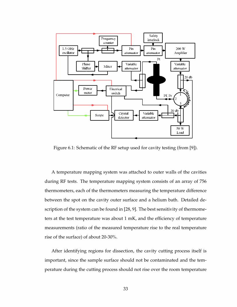
Figure 6.1: Schematic of the RF setup used for cavity testing (from [9]).
A temperature mapping system was attached to outer walls of the cavities
during RF tests. The temperature mapping system consists of an array of 756
thermometers, each of the thermometers measuring the temperature difference
between the spot on the cavity outer surface and a helium bath. Detailed de-
scription of the system can be found in [28, 9]. The best sensitivity of thermome-
ters at the test temperature was about 1 mK, and the efficiency of temperature
measurements (ratio of the measured temperature rise to the real temperature
rise of the surface) of about 20-30%.
After identifying regions for dissection, the cavity cutting process itself is
important, since the sample surface should not be contaminated and the tem-
perature during the cutting process should not rise over the room temperature
33
in the sample central area, since it will effectively bake the sample and thus any
useful information about unique surface structure and its relation to the baking
effect might be destroyed. In this thesis work the automated milling machine
was used for cutting with the pure water as a lubricant. Using water instead
of normally used oil for lubrication is necessary, since it can only expose the
sample surface to the water droplets, which do not effect the high field Q-slope
properties because the high pressure water rinsing was shown not to alter the
HFQS behavior of niobium cavities. Auger electron spectroscopy on the test
sample before and after cutting indicated a slight increase of carbon level as ex-
pected from handling in air, but no foreign contaminants have been introduced
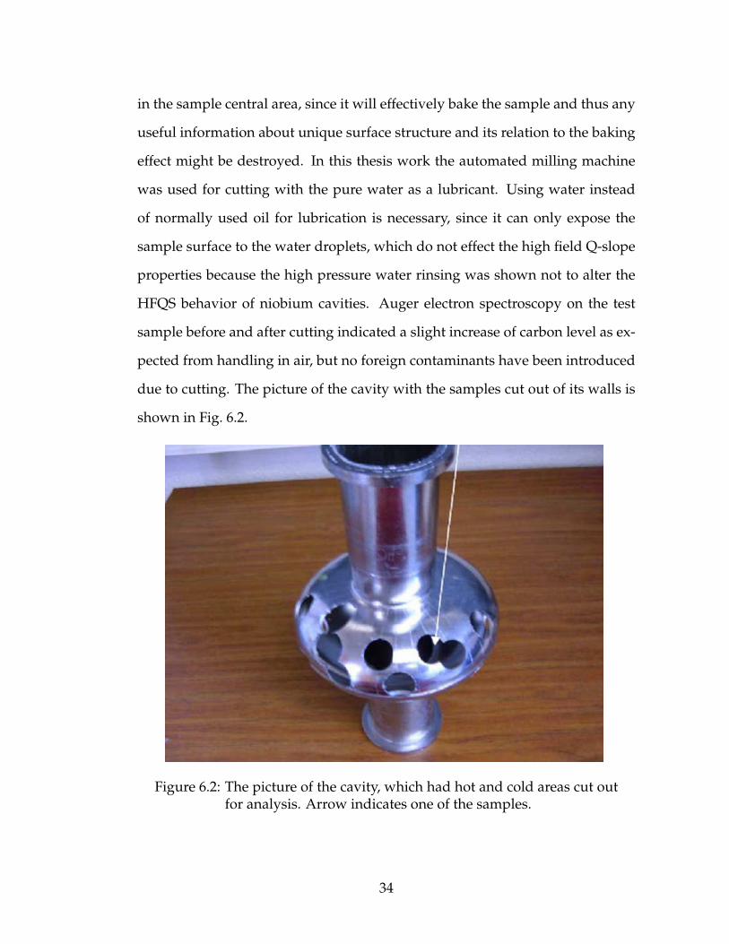
due to cutting. The picture of the cavity with the samples cut out of its walls is
shown in Fig. 6.2.
Figure 6.2: The picture of the cavity, which had hot and cold areas cut outfor analysis. Arrow indicates one of the samples.
34
Samples needed to be cut only from the high magnetic field regions where
the heating due to HFQS is dominant.
6.2 RF tests
6.2.1 Small grain BCP
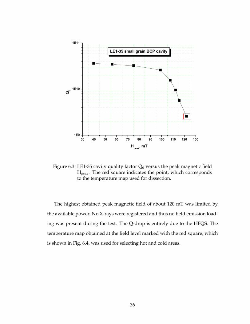
The LE1-35 niobium cavity with a grain size of about 1 mm, which underwent
a BCP treatment, was high pressure water rinsed and tested with the thermom-
etry system attached. The Q0 vs. Hpeak results of the RF test of the cavity are
shown in Fig. 6.3.
35
30 40 50 60 70 80 90 100 110 120 1301E9
1E10
1E11
LE1-35 small grain BCP cavity
Q0
Hpeak, mT
Figure 6.3: LE1-35 cavity quality factor Q0 versus the peak magnetic fieldHpeak. The red square indicates the point, which correspondsto the temperature map used for dissection.
The highest obtained peak magnetic field of about 120 mT was limited by
the available power. No X-rays were registered and thus no field emission load-
ing was present during the test. The Q-drop is entirely due to the HFQS. The
temperature map obtained at the field level marked with the red square, which
is shown in Fig. 6.4, was used for selecting hot and cold areas.
36
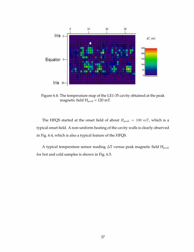
Figure 6.4: The temperature map of the LE1-35 cavity obtained at the peakmagnetic field Hpeak = 120 mT.
The HFQS started at the onset field of about Hpeak = 100 mT , which is a
typical onset field. A non-uniform heating of the cavity walls is clearly observed
in Fig. 6.4, which is also a typical feature of the HFQS.
A typical temperature sensor reading ∆T versus peak magnetic field Hpeak
for hot and cold samples is shown in Fig. 6.5.
37

40 50 60 70 80 90 100 110 120 130
1
10
100
1000
Hot sample Cold sample
LE1-35 small grain BCP cavity
T, m
K
Hpeak, mT
Figure 6.5: Typical ∆T vs. Hpeak curves for LE1-35 small grain BCP cavityhot and cold samples.
Note that HFQS is present in both hot and cold regions. The ratios of the
temperature increase ∆T at the hot areas to the ∆T of the cold areas is about
∆Thot/∆Tcold ≈ 2−10. This ratio will be important later for comparison between
small and large grain BCP and EP cavities.
Based on the temperature map (Fig. 6.4)and the interpolated contour plot
of the temperature distribution (Fig. 6.6), ten hot and ten cold areas were se-
lected for cutting. Each sample was chosen to span the area covered by two
thermometers, so that samples were approximately of a circular shape with the
diameter of about 1.5 cm. The contour plot showing the samples selected for
38
cutting marked by red and white circles for hot and cold areas respectively.
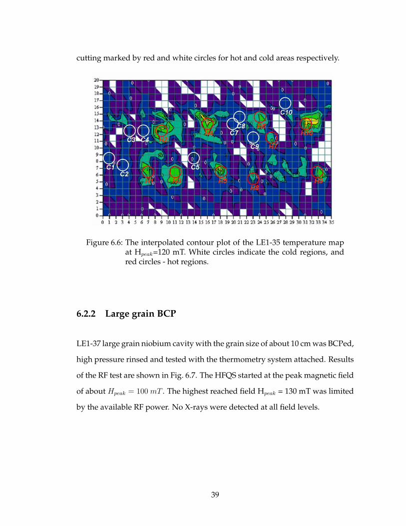
Figure 6.6: The interpolated contour plot of the LE1-35 temperature mapat Hpeak=120 mT. White circles indicate the cold regions, andred circles - hot regions.
6.2.2 Large grain BCP
LE1-37 large grain niobium cavity with the grain size of about 10 cm was BCPed,
high pressure rinsed and tested with the thermometry system attached. Results
of the RF test are shown in Fig. 6.7. The HFQS started at the peak magnetic field
of about Hpeak = 100 mT . The highest reached field Hpeak = 130 mT was limited
by the available RF power. No X-rays were detected at all field levels.
39

0 10 20 30 40 50 60 70 80 90 100 110 120 130 140 1501E9
1E10
1E11
Q0
Hpeak, mT
LE1-37 large grain BCP cavity
Figure 6.7: LE1-37 cavity quality factor Q0 versus the peak magnetic fieldHpeak. The red square indicates the point, which correspondsto the temperature map used for dissection.
Temperature maps were obtained at the each field level in the Q vs. H
curve and the T-map for the highest field reached (marked by the red square
in Fig. 6.7) is presented in Fig. 6.8.
40
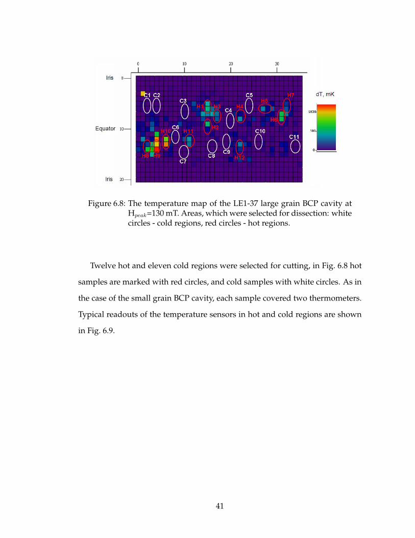
Figure 6.8: The temperature map of the LE1-37 large grain BCP cavity atHpeak=130 mT. Areas, which were selected for dissection: whitecircles - cold regions, red circles - hot regions.
Twelve hot and eleven cold regions were selected for cutting, in Fig. 6.8 hot
samples are marked with red circles, and cold samples with white circles. As in
the case of the small grain BCP cavity, each sample covered two thermometers.
Typical readouts of the temperature sensors in hot and cold regions are shown
in Fig. 6.9.
41

20 40 60 80 100 120 140
1
10
100
1000
Hot sample Cold sample
LE1-37 large grain BCP cavity
T, m
K
Hpeak, mT
Figure 6.9: Typical ∆T vs. Hpeak curves for LE1-37 small grain BCP cavityhot and cold samples.
As one can see both from the temperature map (Fig. 6.8)and from the ∆T
vs. Hpeak curves (Fig. 6.9), the hot spots in the large grain BCP case are stronger
than in the case of the small grain BCP, whereas cold areas have approximately
the same field behavior. The ratio of the maximum temperature increases for
the hot and cold samples in the large grain BCP case is ∆Thot/∆Tcold ≈ 15 − 25,
which is several times that for the small grain BCP one.
42

6.2.3 Small grain EP
The small grain LE1-HOR niobium cavity, which had a grain size of about 1 mm,
was electropolished, high pressure rinsed and tested with the temperature map-
ping system attached. The results of the RF test are shown in Fig. 6.10. During
the test a field emitter turned on after reaching the peak magnetic field of about
Hpeak=120 mT (Epeak=49 MV/m) as was indicated by a significant X-ray radia-
tion level and by the observation of the line heating pattern in the temperature
map as is typical of the field emission [9]. But the data obtained by the time
of the emitter turn-on was taken in the HFQS regime and was sufficient for se-
lecting hot and cold regions for cutting. Quenching at the field emission site
started to happen at the field levels previously reached without it and that was
the ultimate limit for the test.
43

20 30 40 50 60 70 80 90 100 110 120 130 1401E9
1E10
1E11 LE1-HOR small grain EP cavity
Q0
Hpeak, mT
Figure 6.10: LE1-35 cavity quality factor Q0 versus the peak magnetic fieldHpeak. The red square indicates the point, which correspondsto the temperature map used for dissection.
Four hot and five cold areas were selected for dissection based on the tem-
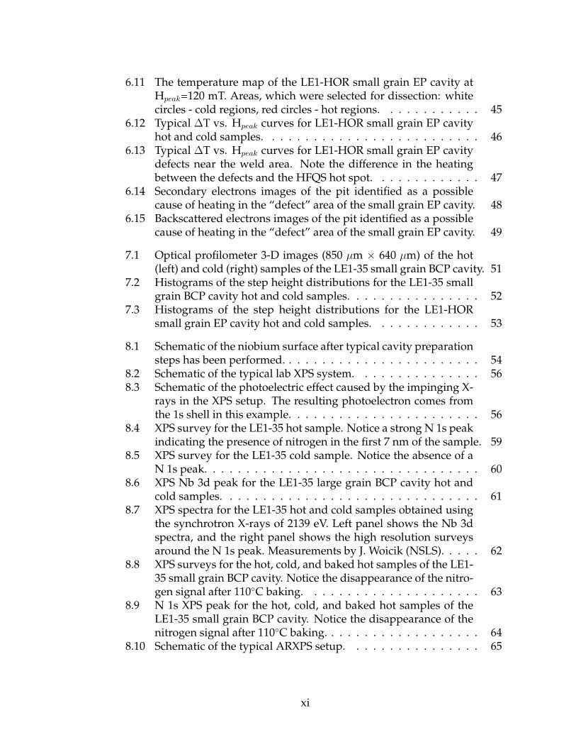
perature map obtained at the highest field, which is shown in Fig. 6.11. Hot
samples are marked with red circles and cold samples with white circles.
44

Figure 6.11: The temperature map of the LE1-HOR small grain EP cavityat Hpeak=120 mT. Areas, which were selected for dissection:white circles - cold regions, red circles - hot regions.
Typical thermometer readings for hot and cold samples are shown in
Fig. 6.12.
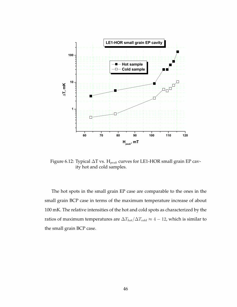
45
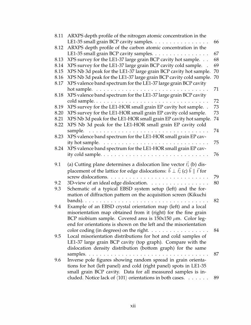
60 70 80 90 100 110 120
1
10
100
Hot sample Cold sample
LE1-HOR small grain EP cavity
T, m
K
Hpeak, mT
Figure 6.12: Typical ∆T vs. Hpeak curves for LE1-HOR small grain EP cav-ity hot and cold samples.
The hot spots in the small grain EP case are comparable to the ones in the
small grain BCP case in terms of the maximum temperature increase of about
100 mK. The relative intensities of the hot and cold spots as characterized by the
ratios of maximum temperatures are ∆Thot/∆Tcold ≈ 4 − 12, which is similar to
the small grain BCP case.
46
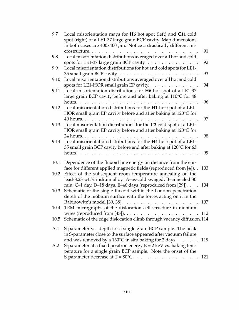
6.2.4 Small grain EP defects
In addition to the high field Q-slope heating, several areas have been identified
on the cavity surface by thermometry (Fig. 6.11), which exhibited a pronounced
heating starting at lower fields below the high field Q-slope onset. Typical de-
pendencies of ∆T vs. Hpeak for the defects close to the weld area are shown in
Fig. 6.13 in comparison with the same curve for the hot sample (H4).
50 60 70 80 90 1001
10
100 Defect Defect #2 Q-slope "hot" spot
Small grain EP cavity defects
T, m
K
Hpeak, mT
Figure 6.13: Typical ∆T vs. Hpeak curves for LE1-HOR small grain EP cav-ity defects near the weld area. Note the difference in the heat-ing between the defects and the HFQS hot spot.
Note the significant difference in the heating of the defect and a hot spot -
the former has increased losses already at lower fields, whereas the latter has
47
almost zero heating up to the HFQS onset field.
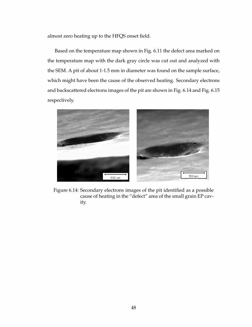
Based on the temperature map shown in Fig. 6.11 the defect area marked on
the temperature map with the dark gray circle was cut out and analyzed with
the SEM. A pit of about 1-1.5 mm in diameter was found on the sample surface,
which might have been the cause of the observed heating. Secondary electrons
and backscattered electrons images of the pit are shown in Fig. 6.14 and Fig. 6.15
respectively.
Figure 6.14: Secondary electrons images of the pit identified as a possiblecause of heating in the “defect” area of the small grain EP cav-ity.
48
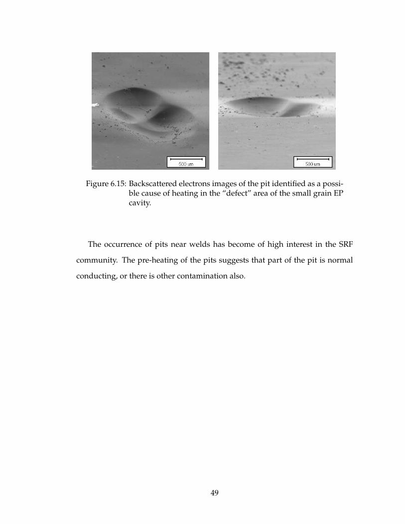
Figure 6.15: Backscattered electrons images of the pit identified as a possi-ble cause of heating in the “defect” area of the small grain EPcavity.
The occurrence of pits near welds has become of high interest in the SRF
community. The pre-heating of the pits suggests that part of the pit is normal
conducting, or there is other contamination also.
49
CHAPTER 7
OPTICAL PROFILOMETRY STUDIES
7.1 Introduction
Niobium cavities typically undergo either BCP or EP chemical treatment as one
of the steps in the final RF surface preparation. The resulting surface is not
perfectly flat but has a finite roughness, with grain boundaries representing the
highest steps due to the dependence of the chemical etching rate on the crys-
talline orientation of the grain. BCP results in the surface, which has larger
(5-10 µm) and steeper grain boundary steps, as compared to the EP surface
(<0.5 µm), as was found by several different studies.
If the step is present on the niobium surface it results in the enhancement of
the magnetic field on the step as discussed in the context of the MFE model for
the HFQS [14]. Since the enhanced magnetic field could produce a premature
local quenching of the grain boundary, a natural explanation for the observed
heating non-uniformity of cavity walls in the HFQS regime would be the differ-
ence in roughness between hot and cold regions. In order to check this hypothe-
sis the roughness measurements have been performed on the dissected hot and
samples to search for any differences. The tool of choice for this purpose was a
non-contact optical profilometry.
A white light optical profilometer was used in this thesis work for character-
izing the surface roughness of the samples. Its operation is based on the interfer-
ometry of light reflected from surface irregularities and the detailed description
is beyond this thesis and can be found in [32].
50

7.2 Experimental data
Several hot and cold samples from the small grain BCP and EP cavities and a
small grain EP cavity were analyzed by the optical profilometer. The output
data of the optical profilometer is a 3D image of the sample surface, which can
be subsequently analyzed by obtaining statistical characteristics such as r.m.s.
roughness etc. or extracting additional characteristics such as line profiles.
In comparing roughness of different samples one should distinguish be-
tween a microroughness, which is a roughness on the length scale smaller than
the grain size, and a macroroughness, which is dominated by the grain bound-
ary steps. Recent studies have shown that the r.m.s. roughness obtained from
the data depends on the dimensions of the area analyzed [46].
Typical images of the hot and cold samples obtained by the optical pro-
filometer are shown in Fig. 7.1. The average r.m.s. micro-roughness of the an-
Figure 7.1: Optical profilometer 3-D images (850 µm × 640 µm) of the hot(left) and cold (right) samples of the LE1-35 small grain BCPcavity.
alyzed samples from both small grain BCP and a small grain EP cavities was
about σ=1.5-1.8 µm for both hot and cold samples, thus the micro-roughness
51

could not be the cause of the different behavior of samples in high RF magnetic
fields.
In order to compare the macro-roughness six line profiles were obtained on
each sample with each profile spanning about 1 cm in length as compared to the
average grain size of 1 mm for the samples. A simple software was developed,
which took the line profile as an input, and produced a number of the steps
having the step height of 1,2,3,... µm. The resulting data for the small grain BCP
cavity samples is summarized in histograms in Fig. 7.2.
Figure 7.2: Histograms of the step height distributions for the LE1-35 smallgrain BCP cavity hot and cold samples.
The corresponding data for the small grain EP cavity is shown in Fig. 7.3.
52
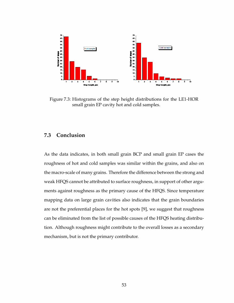
Figure 7.3: Histograms of the step height distributions for the LE1-HORsmall grain EP cavity hot and cold samples.
7.3 Conclusion
As the data indicates, in both small grain BCP and small grain EP cases the
roughness of hot and cold samples was similar within the grains, and also on
the macro-scale of many grains. Therefore the difference between the strong and
weak HFQS cannot be attributed to surface roughness, in support of other argu-
ments against roughness as the primary cause of the HFQS. Since temperature
mapping data on large grain cavities also indicates that the grain boundaries
are not the preferential places for the hot spots [9], we suggest that roughness
can be eliminated from the list of possible causes of the HFQS heating distribu-
tion. Although roughness might contribute to the overall losses as a secondary
mechanism, but is not the primary contributor.
53
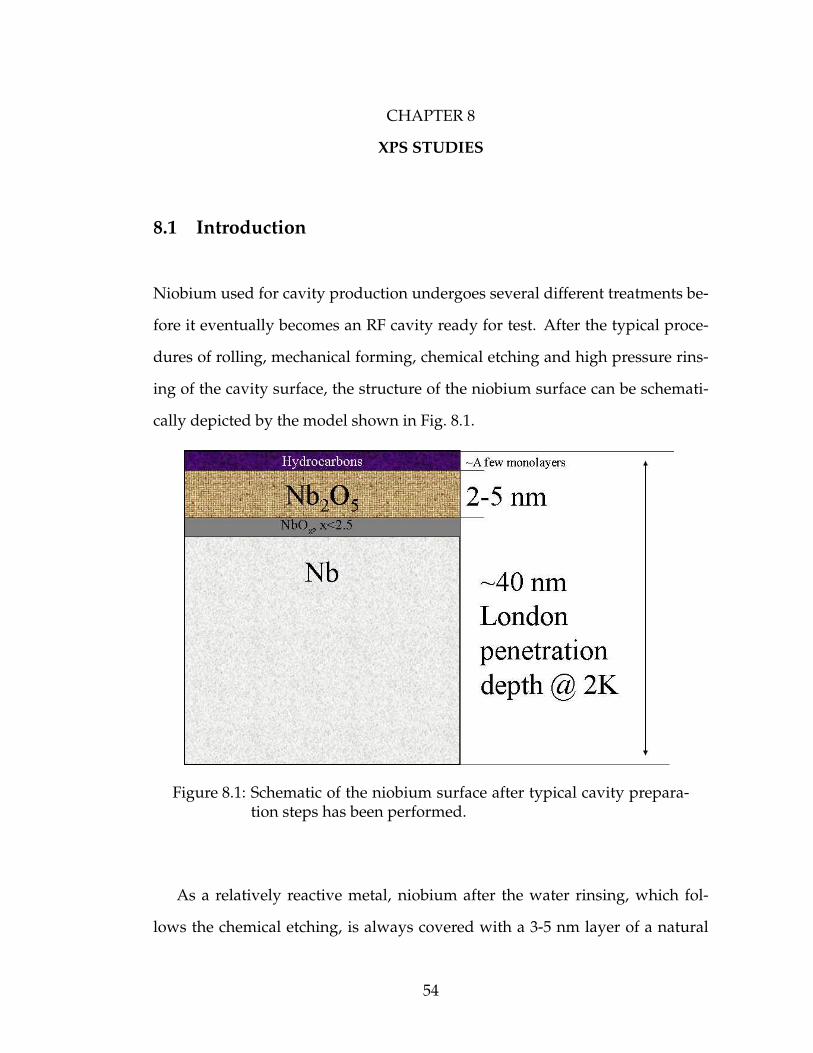
CHAPTER 8
XPS STUDIES
8.1 Introduction
Niobium used for cavity production undergoes several different treatments be-
fore it eventually becomes an RF cavity ready for test. After the typical proce-
dures of rolling, mechanical forming, chemical etching and high pressure rins-
ing of the cavity surface, the structure of the niobium surface can be schemati-
cally depicted by the model shown in Fig. 8.1.
Figure 8.1: Schematic of the niobium surface after typical cavity prepara-tion steps has been performed.
As a relatively reactive metal, niobium after the water rinsing, which fol-
lows the chemical etching, is always covered with a 3-5 nm layer of a natural
54

oxide predominantly in the form of Nb2O5. The oxide layer is initially formed
during a wet oxidation in water after the chemical treatment such as BCP or
EP. The following air exposure of the cavity results in the slow increase of the
oxide thickness until the process stops at about 4-5 nm oxide thickness. In the
transition region, where the natural oxide meets the bulk niobium, suboxides in
the form of NbO and NbO2 may also be present, although the exact amount is
uncertain.
In addition to the oxide, contaminants such as hydrocarbons, water, and
chemical residues (F, N, . . . ) might be present within the first several nanome-
ters of niobium, which can be introduced during chemical etching and other
steps of cavity preparation.
Thus, it is important to compare elemental compositions and chemical struc-
tures for the hot and cold samples within first several nanometers to check if
there are any differences, which might be responsible for their different behav-
ior at high magnetic fields.
A tool, which is suitable to provide this information, is an X-ray Photoelec-
tron Spectroscopy (XPS), also referred to as Electron Spectroscopy for Chemical
Analysis (ESCA). In the typical XPS system, such as one shown in Fig. 8.2, a
sample is irradiated with the focused X-ray beam of 1 − 2 keV energy, which
results in some of the core shell electrons being knocked off as shown in Fig. 8.3.
55
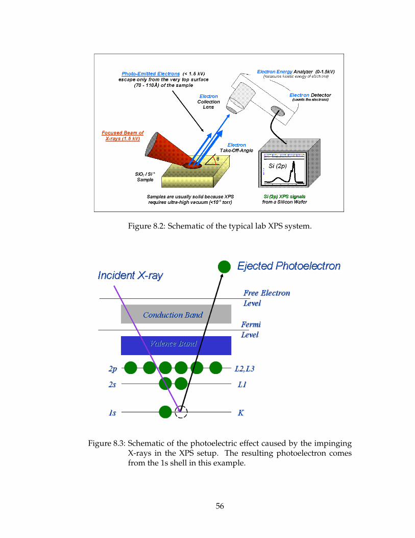
Figure 8.2: Schematic of the typical lab XPS system.
Figure 8.3: Schematic of the photoelectric effect caused by the impingingX-rays in the XPS setup. The resulting photoelectron comesfrom the 1s shell in this example.
56
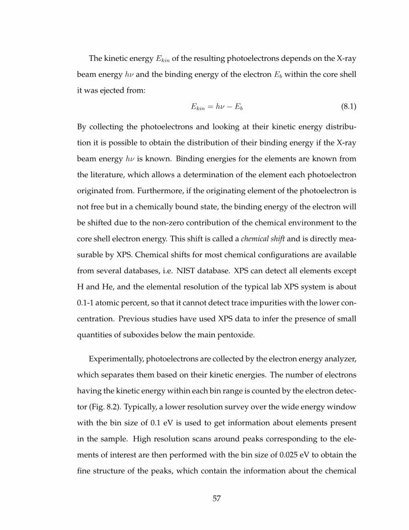
The kinetic energy Ekin of the resulting photoelectrons depends on the X-ray
beam energy hν and the binding energy of the electron Eb within the core shell
it was ejected from:
Ekin = hν − Eb (8.1)
By collecting the photoelectrons and looking at their kinetic energy distribu-
tion it is possible to obtain the distribution of their binding energy if the X-ray
beam energy hν is known. Binding energies for the elements are known from
the literature, which allows a determination of the element each photoelectron
originated from. Furthermore, if the originating element of the photoelectron is
not free but in a chemically bound state, the binding energy of the electron will
be shifted due to the non-zero contribution of the chemical environment to the
core shell electron energy. This shift is called a chemical shift and is directly mea-
surable by XPS. Chemical shifts for most chemical configurations are available
from several databases, i.e. NIST database. XPS can detect all elements except
H and He, and the elemental resolution of the typical lab XPS system is about
0.1-1 atomic percent, so that it cannot detect trace impurities with the lower con-
centration. Previous studies have used XPS data to infer the presence of small
quantities of suboxides below the main pentoxide.
Experimentally, photoelectrons are collected by the electron energy analyzer,
which separates them based on their kinetic energies. The number of electrons
having the kinetic energy within each bin range is counted by the electron detec-
tor (Fig. 8.2). Typically, a lower resolution survey over the wide energy window
with the bin size of 0.1 eV is used to get information about elements present
in the sample. High resolution scans around peaks corresponding to the ele-
ments of interest are then performed with the bin size of 0.025 eV to obtain the
fine structure of the peaks, which contain the information about the chemical
57

environment, as described above.
Hot and cold samples from all the cavities, which were dissected, were an-
alyzed using the lab SSX-100 XPS system utilizing the Al Kα X-ray source of
1486.6 eV energy. The angle between the electron energy analyzer and a sample
normal was fixed at 55. The radius of the spot for the X-ray beam was 800 µm.
Photoelectrons have the limited escape depth due to their interaction with
the atoms constituting the sample, which is dependent on the inelastic mean
free path (IMFP) λ. The information depth d0, which is the escape depth of
photoelectrons, is generally defined to be d0 = 3λ. The IMFP is calculated using
the simulation software and for photoelectrons resulting from the 1486.6 eV X-
rays in niobium the information depth was calculated to be about 7 nm, which
covers the oxide and the oxide/metal interface.
8.2 Small grain BCP cavity samples
All samples have been analyzed by the same procedure using the lab XPS sys-
tem described above. For each sample several measurements have been per-
formed at three different spots at the sample surface:
• A low resolution survey spanning the electron binding energies from 0 to
1000 eV for general analysis of the elements present
• The high resolution spectra acquisition for C 1s, O 1s, N 1s, Nb 3d, and a
valence band for the information on chemical bonding
58

General XPS surveys revealed that three out of ten hot samples had a strong
N 1s signal present in the survey at the level of a few atomic percents. An exam-
ple of the survey from one of the hot samples containing nitrogen is shown in
Fig. 8.4. The corresponding typical survey for cold samples is shown in Fig. 8.5.
One can notice that in the hot sample survey the N 1s peak is present at about
401 eV binding energy whereas the cold one does not have it.
Figure 8.4: XPS survey for the LE1-35 hot sample. Notice a strong N 1speak indicating the presence of nitrogen in the first 7 nm of thesample.
59

Figure 8.5: XPS survey for the LE1-35 cold sample. Notice the absence ofa N 1s peak.
The N 1s peak at 401 eV might correspond to the adsorbed NOδ− [31], which
can be introduced during the BCP treatment where nitric acid HNO3 is one of
the BCP solution constituents.
For the analysis of the niobium oxide structure the high resolution spectrum
around Nb 3d peak was obtained for all samples. Typical data for hot and cold
samples is shown in Fig. 8.6. No difference within the instrument resolution
was observed in the oxide structure of all hot and cold samples.
60

220 215 210 205 200 195
Nb0
Nb5+
Hot sample Cold sample
Cou
nts,
a.u
.
Binding energy, eV
Figure 8.6: XPS Nb 3d peak for the LE1-35 large grain BCP cavity hot andcold samples.
In addition to the lab XPS analysis, a collaboration with Joseph Woicik from
BNL National Synchrotron Light Source (NSLS) was established to obtain the
XPS spectra using the synchrotron X-ray source, which provides a greater en-
ergy resolution and a higher energy of the X-ray beam. The X-ray beam with
the higher energy produces photoelectrons with the higher kinetic energy as
follows from Eq. (8.1). The higher kinetic energy of the photoelectrons in turn
translates into the higher escape depth. XPS spectra acquisition was performed
using the X-ray energy of 2139 eV, which provides information about first 10 nm
of the niobium surface, as compared to only 7 nm for the lab XPS system. Thus,
for the synchrotron energy used, the XPS spectrum is less dominated by the
niobium oxide signal, but includes a significant contribution from about 6 nm
of bulk niobium underneath the oxide.
61

The resulting XPS spectra obtained on the hot and cold samples are shown
in Fig. 8.7.
Figure 8.7: XPS spectra for the LE1-35 hot and cold samples obtained usingthe synchrotron X-rays of 2139 eV. Left panel shows the Nb 3dspectra, and the right panel shows the high resolution surveysaround the N 1s peak. Measurements by J. Woicik (NSLS).
The obtained spectra confirmed the conclusion reached after analyzing the
lab XPS data that the niobium oxide structure is identical in hot and cold sam-
ples, and the only difference inferred from XPS investigations is the presence of
nitrogen in the hot sample.
62
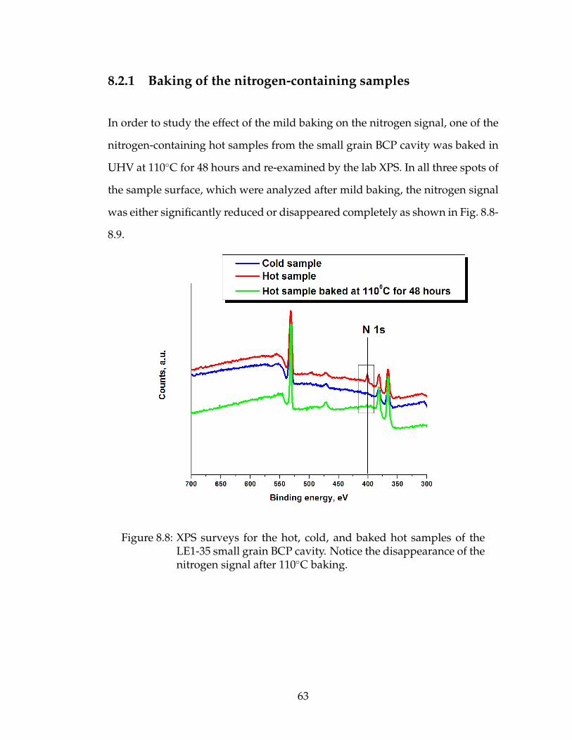
8.2.1 Baking of the nitrogen-containing samples
In order to study the effect of the mild baking on the nitrogen signal, one of the
nitrogen-containing hot samples from the small grain BCP cavity was baked in
UHV at 110C for 48 hours and re-examined by the lab XPS. In all three spots of
the sample surface, which were analyzed after mild baking, the nitrogen signal
was either significantly reduced or disappeared completely as shown in Fig. 8.8-
8.9.
Figure 8.8: XPS surveys for the hot, cold, and baked hot samples of theLE1-35 small grain BCP cavity. Notice the disappearance of thenitrogen signal after 110C baking.
63

Figure 8.9: N 1s XPS peak for the hot, cold, and baked hot samples of theLE1-35 small grain BCP cavity. Notice the disappearance of thenitrogen signal after 110C baking.
8.2.2 Angle-resolved XPS studies
In order to study the distribution of nitrogen within the information depth of
the XPS signal the angle-resolved technique was implemented in the lab XPS
system. The schematic of the typical ARXPS setup is shown in Fig. 8.10.
64

Figure 8.10: Schematic of the typical ARXPS setup.
The angle-resolved XPS (ARXPS) is based on the dependence of the maxi-
mum depth, from which the photoelectrons are reaching the analyzer, on the
angle between the electron energy analyzer axis and a sample normal:
d = d0 × cosα (8.2)
where d0 is the maximum escape depth of photoelectrons reaching the analyzer
if it is at 0 angle with the sample normal, and α is the angle between the electron
analyzer axis and the sample normal. The maximum escape depth d0 is deter-
mined by the photoelectron kinetic energy, which in turn depends on the X-ray
beam energy and the binding energy of the electron shell the photoelectron is
originated from as follows from Eq. (8.1).
By measuring XPS spectra at different angles between the electron analyzer
and the sample normal it is possible to reconstruct the depth profile using the
Eq. (8.2).
65
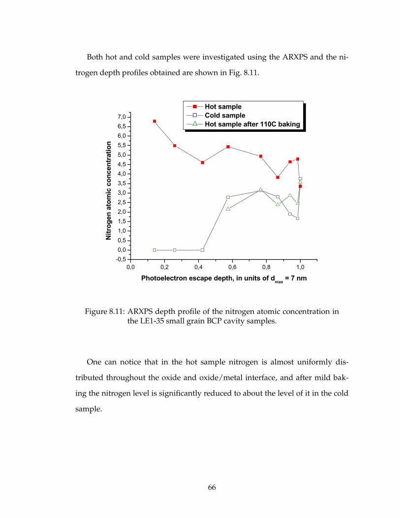
Both hot and cold samples were investigated using the ARXPS and the ni-
trogen depth profiles obtained are shown in Fig. 8.11.
0,0 0,2 0,4 0,6 0,8 1,0-0,50,00,51,01,52,02,53,03,54,04,55,05,56,06,57,0
Nitr
ogen
ato
mic
con
cent
ratio
n
Photoelectron escape depth, in units of dmax = 7 nm
Hot sample Cold sample Hot sample after 110C baking
Figure 8.11: ARXPS depth profile of the nitrogen atomic concentration inthe LE1-35 small grain BCP cavity samples.
One can notice that in the hot sample nitrogen is almost uniformly dis-
tributed throughout the oxide and oxide/metal interface, and after mild bak-
ing the nitrogen level is significantly reduced to about the level of it in the cold
sample.
66

0,0 0,2 0,4 0,6 0,8 1,020
30
40
50
60
70
80
Car
bon
atom
ic c
once
ntra
tion
Photoelectron escape depth, in units of dmax = 7 nm
Hot sample Cold sample Hot sample after 110C baking
Figure 8.12: ARXPS depth profile of the carbon atomic concentration in theLE1-35 small grain BCP cavity samples.
Carbon profiles before and after mild baking show that the carbon concen-
tration almost did not change. But one should be careful with the carbon con-
centration interpretation since carbon is a common contaminant, which is in-
evitably present on the surface of samples in the form of hydrocarbons, and its
concentration depends strongly on the handling history of the sample and also
varies significantly over the surface of the sample.
67
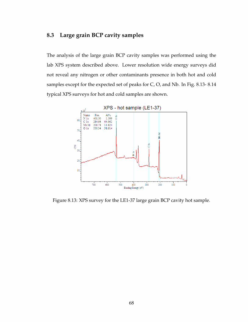
8.3 Large grain BCP cavity samples
The analysis of the large grain BCP cavity samples was performed using the
lab XPS system described above. Lower resolution wide energy surveys did
not reveal any nitrogen or other contaminants presence in both hot and cold
samples except for the expected set of peaks for C, O, and Nb. In Fig. 8.13- 8.14
typical XPS surveys for hot and cold samples are shown.
Figure 8.13: XPS survey for the LE1-37 large grain BCP cavity hot sample.
68
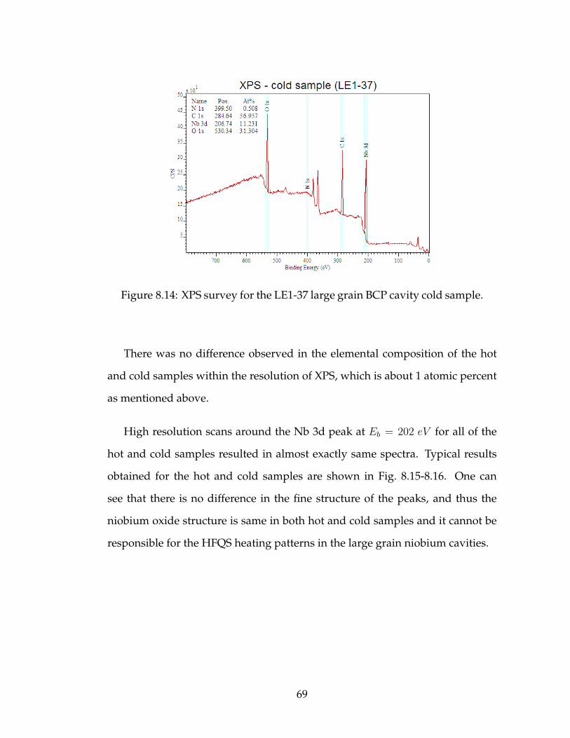
Figure 8.14: XPS survey for the LE1-37 large grain BCP cavity cold sample.
There was no difference observed in the elemental composition of the hot
and cold samples within the resolution of XPS, which is about 1 atomic percent
as mentioned above.
High resolution scans around the Nb 3d peak at Eb = 202 eV for all of the
hot and cold samples resulted in almost exactly same spectra. Typical results
obtained for the hot and cold samples are shown in Fig. 8.15-8.16. One can
see that there is no difference in the fine structure of the peaks, and thus the
niobium oxide structure is same in both hot and cold samples and it cannot be
responsible for the HFQS heating patterns in the large grain niobium cavities.
69
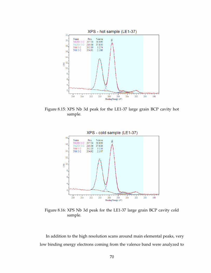
Figure 8.15: XPS Nb 3d peak for the LE1-37 large grain BCP cavity hotsample.
Figure 8.16: XPS Nb 3d peak for the LE1-37 large grain BCP cavity coldsample.
In addition to the high resolution scans around main elemental peaks, very
low binding energy electrons coming from the valence band were analyzed to
70

study the oxidation states. Typical results for the hot and cold samples are
shown in Fig. 8.17- 8.18. Since the valence band spectrum is unique for each
particular elemental composition and its oxidation state, we can once again see
that there is no difference in the chemical structure of the hot and cold samples.
Figure 8.17: XPS valence band spectrum for the LE1-37 large grain BCPcavity hot sample.
71
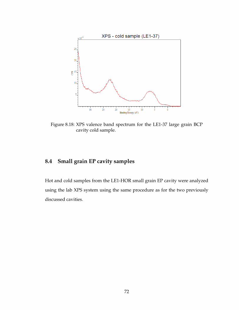
Figure 8.18: XPS valence band spectrum for the LE1-37 large grain BCPcavity cold sample.
8.4 Small grain EP cavity samples
Hot and cold samples from the LE1-HOR small grain EP cavity were analyzed
using the lab XPS system using the same procedure as for the two previously
discussed cavities.
72
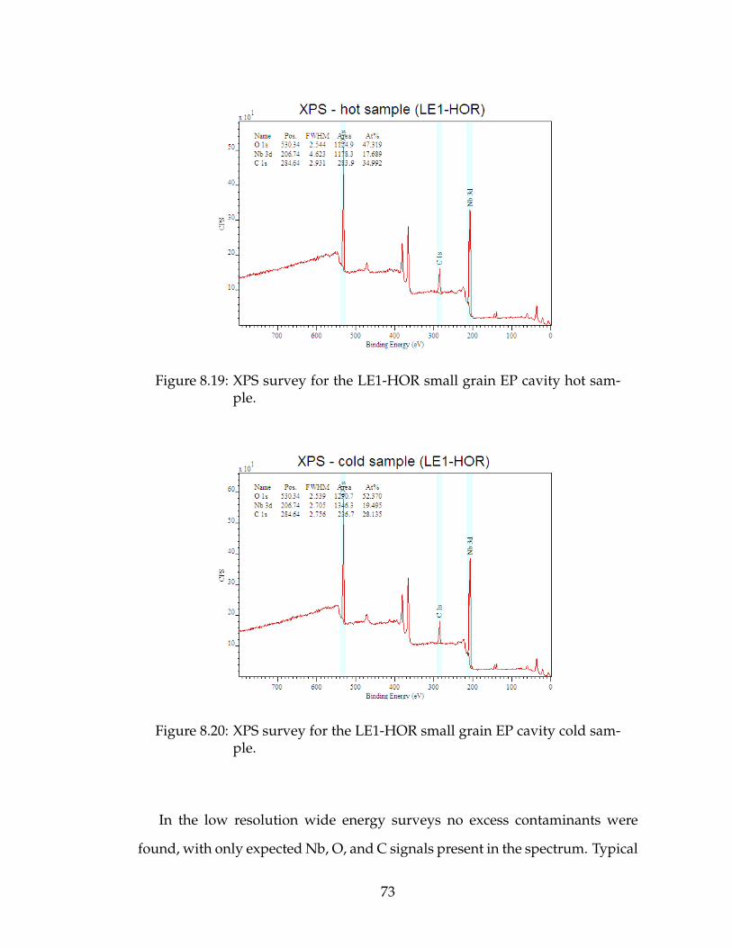
Figure 8.19: XPS survey for the LE1-HOR small grain EP cavity hot sam-ple.
Figure 8.20: XPS survey for the LE1-HOR small grain EP cavity cold sam-ple.
In the low resolution wide energy surveys no excess contaminants were
found, with only expected Nb, O, and C signals present in the spectrum. Typical
73
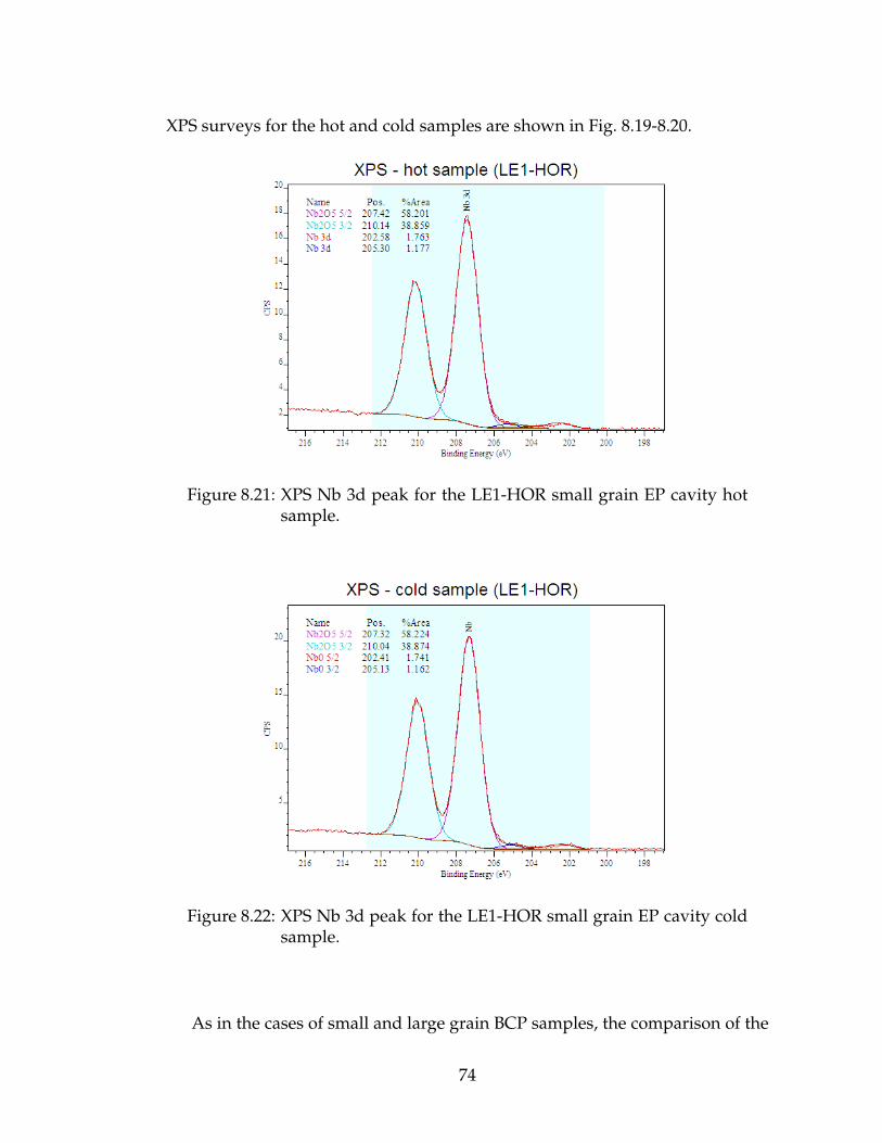
XPS surveys for the hot and cold samples are shown in Fig. 8.19-8.20.
Figure 8.21: XPS Nb 3d peak for the LE1-HOR small grain EP cavity hotsample.
Figure 8.22: XPS Nb 3d peak for the LE1-HOR small grain EP cavity coldsample.
As in the cases of small and large grain BCP samples, the comparison of the
74
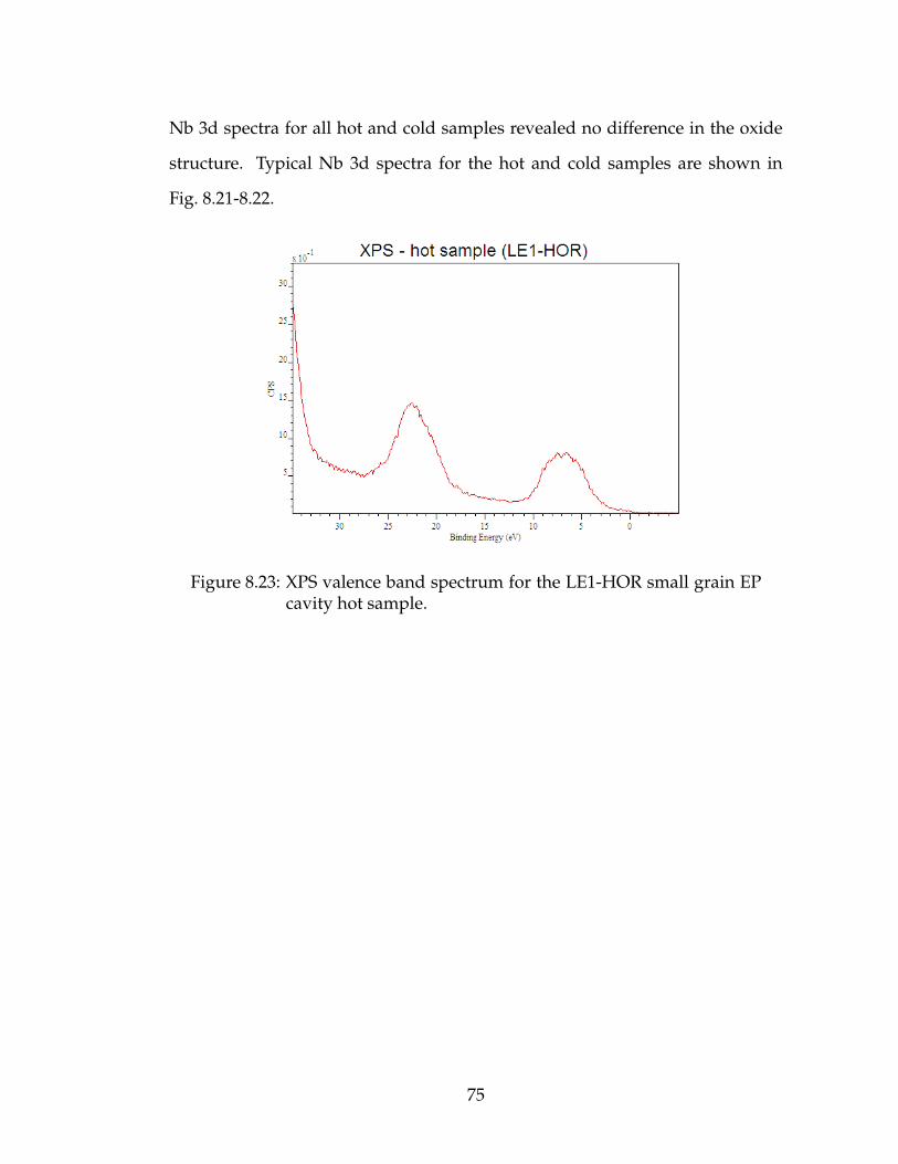
Nb 3d spectra for all hot and cold samples revealed no difference in the oxide
structure. Typical Nb 3d spectra for the hot and cold samples are shown in
Fig. 8.21-8.22.
Figure 8.23: XPS valence band spectrum for the LE1-HOR small grain EPcavity hot sample.
75
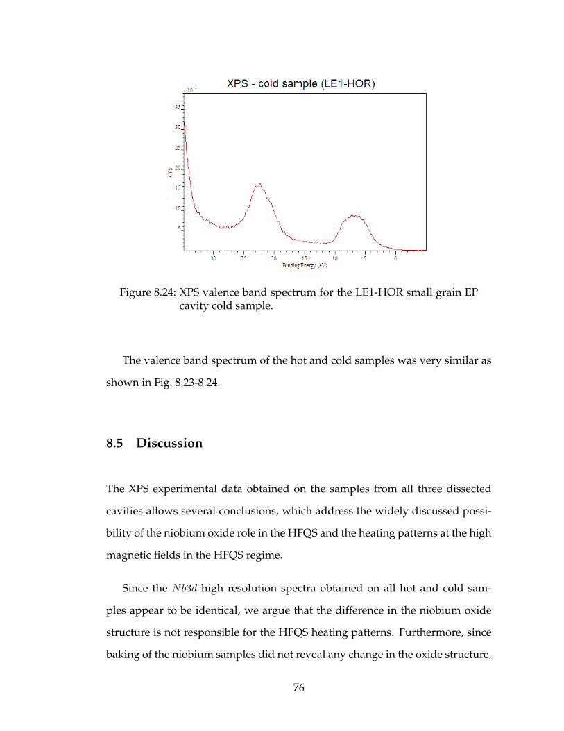
Figure 8.24: XPS valence band spectrum for the LE1-HOR small grain EPcavity cold sample.
The valence band spectrum of the hot and cold samples was very similar as
shown in Fig. 8.23-8.24.
8.5 Discussion
The XPS experimental data obtained on the samples from all three dissected
cavities allows several conclusions, which address the widely discussed possi-
bility of the niobium oxide role in the HFQS and the heating patterns at the high
magnetic fields in the HFQS regime.
Since the Nb3d high resolution spectra obtained on all hot and cold sam-
ples appear to be identical, we argue that the difference in the niobium oxide
structure is not responsible for the HFQS heating patterns. Furthermore, since
baking of the niobium samples did not reveal any change in the oxide structure,
76

we suggest that the oxide can be ruled out as a possible cause of the HFQS as
well. This conclusion was also confirmed by the XPS studies reported in [12],
where it was shown that samples after baking and air exposure have exactly
same oxide structure as before baking. Valence band spectra obtained on hot
and cold samples from large grain BCP and small grain EP cavities confirm that
the chemical state of niobium is the same in the samples, at least at the level of
XPS sensitivity.
In the case of non-oxygen contaminants, in the small grain BCP cavity it
was discovered that hot samples, which exhibited the highest temperature in-
crease during the RF test in the HFQS regime, contained a strong nitrogen signal
present within the first 7-10 nm of the surface. Mild baking of the nitrogen-
containing sample resulted in the disappearance of the nitrogen signal in the
XPS spectrum. If we assume that the mechanism of the nitrogen motion during
mild baking is the bulk diffusion, than the observed change is not possible due
to a small value of the nitrogen diffusion length as calculated from its bulk dif-
fusion coefficient found in the literature [1]. But it is known that the diffusion of
impurities such as nitrogen can go through grain boundaries or dislocations at a
much higher rate than through the bulk, which we suggest might be happening
in our case for the diffusion of N from the oxide into the bulk.
The “oxide purifier” model proposed recently for the mild baking effect [9]
requires the carbon concentration after mild baking to increase in the oxide
layer, since carbon is suggested to diffuse from the bulk niobium into the ox-
ide. But ARXPS experiments show that carbon distribution before and after
mild baking of the hot sample does not appear to change much at the 4-7 nm
depth, which contradicts the model.
77

CHAPTER 9
EBSD STUDIES ON CAVITY SAMPLES
9.1 Introduction
Niobium is a crystalline material with the body-centered cubic (BCC) lattice
structure. In general in any crystalline body different types of crystalline defects
are inevitably present, i.e.
• Point defects: vacancies, substitutional impurities, interstitial impurities
• Linear defects: dislocations (edge, screw and mixed types)
• Planar defects: grain boundaries, interfaces
• Bulk defects: precipitates, voids, cracks
Crystalline microstructure of type II superconductors within London field pene-
tration depth λ is known to have an important effect on a multitude of magnetic
flux penetration and flux motion phenomena in the superconducting state, such
as flux flow, flux pinning, flux creep etc. Thus it is important to analyze hot and
cold samples with the tool that provides information about the microstructure
in order to elucidate any difference, which might be responsible for the HFQS
heating patterns.
Such a tool, which was developed recently, is an Electron Backscatter Diffrac-
tion (EBSD).
78

9.1.1 Dislocations
A dislocation is a linear defect of the crystalline lattice. There are two basic
types of dislocations: edge and screw. In order to visualize ideal dislocations the
following procedure is usually suggested: make a cut into an ideal crystal along
some plane (Fig. 9.1), then the dislocation line is by definition ~t, displace atoms
by a lattice vector along the direction perpendicular or parallel to the cut plane,
“weld” the crystal back together. The resulting distortion is an edge dislocation
if~b ⊥ ~t and a screw dislocation if~b ‖ ~t.
Figure 9.1: (a) Cutting plane determines a dislocation line vector ~t; (b) dis-placement of the lattice for edge dislocations: ~b ⊥ ~t; (c)~b ‖ ~t forscrew dislocations.
In Fig. 9.2 a 3D view of an ideal edge dislocation is shown. One can see that
an edge dislocation might be interpreted as a missing atomic half-plane in the
crystal.
79
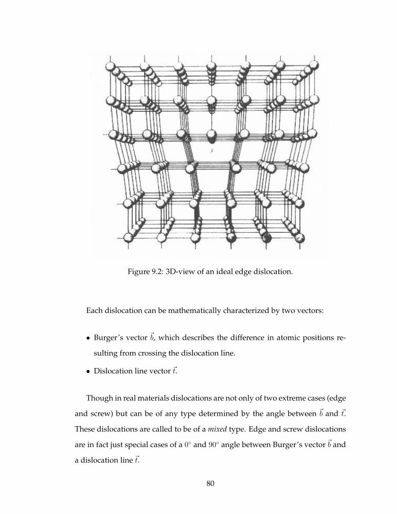
Figure 9.2: 3D-view of an ideal edge dislocation.
Each dislocation can be mathematically characterized by two vectors:
• Burger’s vector ~b, which describes the difference in atomic positions re-
sulting from crossing the dislocation line.
• Dislocation line vector ~t.
Though in real materials dislocations are not only of two extreme cases (edge
and screw) but can be of any type determined by the angle between ~b and ~t.
These dislocations are called to be of a mixed type. Edge and screw dislocations
are in fact just special cases of a 0 and 90 angle between Burger’s vector~b and
a dislocation line ~t.
80

As was shown at the dawn of dislocation theory [45, 34, 37] by studies of
solid materials under applied stress, any plastic deformation of crystalline bod-
ies is accommodated by dislocations, which are created during deformation and
their motion allows to preserve the crystal continuity while accommodating the
change of geometrical dimensions.
9.2 Electron back-scattered diffraction
Electron back-scattered diffraction (EBSD) is a recently developed technique,
which relies on the diffraction of backscattered electrons from the sample sur-
face for identifying the crystalline lattice structure. An EBSD system is usually
built upon the existing scanning electron microscope (SEM) system. The sam-
ple is typically mounted within the SEM chamber with the angle of about 70
made between the electron beam and a sample surface normal. Backscattered
electrons are captured by a phosphorous screen, with the resulting diffraction
pattern of Kikuchi bands produced. Detailed description of the physics behind
Kikuchi bands formation is beyond the scope of this thesis and can be found
in [44]. The image on the screen is captured by a fast camera, and then analyzed
by the software that indexes Kikuchi bands assigning a crystalline orientation
gij to the observed diffraction pattern based on the material parameters such
as unit cell length. Each measurement in modern EBSD systems takes about
0.1-0.5 seconds. Moving the beam across the analysis area in a regular pattern
(e.g. square or hexagonal) with orientation measurements at each spot produces
a 2D-map of crystalline orientations. A schematic of a typical EBSD system
setup is shown in Fig. 9.3.
81
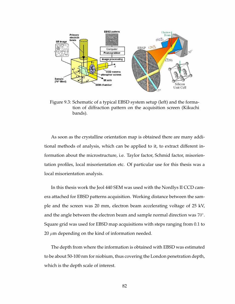
Figure 9.3: Schematic of a typical EBSD system setup (left) and the forma-tion of diffraction pattern on the acquisition screen (Kikuchibands).
As soon as the crystalline orientation map is obtained there are many addi-
tional methods of analysis, which can be applied to it, to extract different in-
formation about the microstructure, i.e. Taylor factor, Schmid factor, misorien-
tation profiles, local misorientation etc. Of particular use for this thesis was a
local misorientation analysis.
In this thesis work the Jeol 440 SEM was used with the Nordlys II CCD cam-
era attached for EBSD patterns acquisition. Working distance between the sam-
ple and the screen was 20 mm, electron beam accelerating voltage of 25 kV,
and the angle between the electron beam and sample normal direction was 70.
Square grid was used for EBSD map acquisitions with steps ranging from 0.1 to
20 µm depending on the kind of information needed.
The depth from where the information is obtained with EBSD was estimated
to be about 50-100 nm for niobium, thus covering the London penetration depth,
which is the depth scale of interest.
82
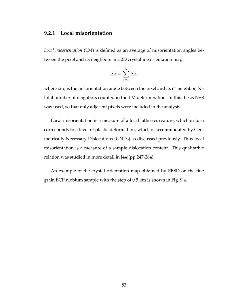
9.2.1 Local misorientation
Local misorientation (LM) is defined as an average of misorientation angles be-
tween the pixel and its neighbors in a 2D crystalline orientation map:
∆α =N∑
i=1
∆αi
where ∆αi is the misorientation angle between the pixel and its ith neighbor, N -
total number of neighbors counted in the LM determination. In this thesis N=8
was used, so that only adjacent pixels were included in the analysis.
Local misorientation is a measure of a local lattice curvature, which in turn
corresponds to a level of plastic deformation, which is accommodated by Geo-
metrically Necessary Dislocations (GNDs) as discussed previously. Thus local
misorientation is a measure of a sample dislocation content. This qualitative
relation was studied in more detail in [44](pp.247-264).
An example of the crystal orientation map obtained by EBSD on the fine
grain BCP niobium sample with the step of 0.5 µm is shown in Fig. 9.4.
83

Figure 9.4: Example of an EBSD crystal orientation map (left) and a localmisorientation map obtained from it (right) for the fine grainBCP niobium sample. Covered area is 150x150 µm. Color leg-end for orientations is shown on the left and the misorientationcolor coding (in degrees) on the right.
The upper left panel shows the crystalline orientation map at each pixel of
the map depicted by a particular color. Correspondence between colors and
orientations is shown in the lower left inverse pole figure, where color basically
codes the angle of misorientation between the spot and three standard orienta-
tions: 〈001〉, 〈011〉, and 〈111〉.
The upper right map shows the local misorientation at each pixel calculated
as outlined above. Color representation is used, with the legend shown below
84

the map, so that, for example, zero local misorientations correspond to a dark
blue color, and misorientations of about 2 are shown by a green color.
9.2.2 Geometrically necessary dislocation content
Recent development of EBSD data analysis techniques allows obtaining the dis-
location tensor from crystalline orientation data.
Local dislocation density tensor, which was introduced by Nye [33], de-
scribes the dislocation content concisely:
αij =K∑
i=1
ρi(bi ⊗ zi) (9.1)
where ~zi indicates the dislocation direction, ~bt is a Burgers vector, and ρi is a
density of dislocations of type i. Assuming zero elastic strain, any crystal con-
taining non-zero dislocation density should have local lattice rotations, which
can be measured by EBSD. The relation between the Nye dislocation tensor and
lattice disorientations between neighboring points then can be approximated as
follows:
αij = eiklgjl,k (9.2)
which is known from EBSD data of orientations gij at each spot. Eq. (9.1) can be
reduced [36] to:
αi = Aikρk
where matrix A represents a component of dislocation dyadic ~b ⊗ ~z. Applying
L2 minimization method the solution can be written explicitly for dislocation
density tensor [36]:
ρGND = AT (AAT )−1α
85

MatLAB software based on this method developed by R. Fertig [20] was used
in order to extract average dislocation density from EBSD orientation maps in
this thesis.
9.2.3 Equivalence of LM and GND density characterizations
Local misorientation as measured by the procedure outlined above is a measure
of the local lattice curvature, which is directly connected to the dislocation den-
sity tensor. So it is important to check this connection explicitly by calculating
both local misorientation distributions and GND density distributions for same
samples. We chose hot and cold samples from the LE1-37 large grain cavity for
this analysis.
86
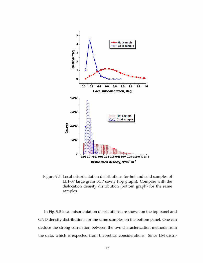
Figure 9.5: Local misorientation distributions for hot and cold samples ofLE1-37 large grain BCP cavity (top graph). Compare with thedislocation density distribution (bottom graph) for the samesamples.
In Fig. 9.5 local misorientation distributions are shown on the top panel and
GND density distributions for the same samples on the bottom panel. One can
deduce the strong correlation between the two characterization methods from
the data, which is expected from theoretical considerations. Since LM distri-
87
butions are easier to obtain and contain essentially the same information, they
are going to be used for dislocation content comparisons between the samples
throughout the thesis.
9.3 Crystalline orientation role in HFQS heating patterns
One of the possible explanations for the heating patterns in the HFQS regime
suggested recently was based on the assumption that some grain orientations
have lower critical field and/or higher surface resistance than others. Small
grain BCP cavity (LE1-35) samples were studied with EBSD in order to check
this hypothesis. Texture analysis was performed by getting EBSD maps of sam-
ples with a relatively large step of 10-20 µm and then analyzing orientation
maps using orientation distribution functions (ODFs) and inverse pole figures
(IPFs).
In Fig. 9.6 inverse polar figures obtained by merging all the data obtained
for hot (left panel) and cold (right panel) samples are shown. Poles represent
three basic crystalline orientations - 〈001〉, 〈101〉 and 〈111〉. Distance from pixel
to the pole corresponds to the magnitude of the misorientation angle between
the basic orientation of the pole and the pixel.
88

Figure 9.6: Inverse pole figures showing random spread in grain orienta-tions for hot (left panel) and cold (right panel) spots in LE1-35small grain BCP cavity. Data for all measured samples is in-cluded. Notice lack of 〈101〉 orientations in both cases.
It is apparent that there is no preferential orientation in either case. Lack of
〈101〉 orientations can be noticed in both hot and cold samples, which is prob-
ably due to sheet rolling and cells forming history. All other orientations are
randomly distributed.
Although even single grain cavities show non-uniform losses as determined
by thermometry, which already undermines the hypothesis of a crystalline ori-
entation as a main underlying factor for the effect, we provide further direct
experimental proof that the hypothesis does not hold and preferential grain ori-
entations are not responsible for the heating non-uniformity in the HFQS.
9.4 Difference between hot and cold samples
As an introductory remark we want to emphasize an important point from the
chapters above on the relative intensity of hot and cold regions in cavities of
different grain sizes. The largest difference between hot and cold spots was
89

observed in the large grain BCP case (∆Thot/∆Tcold ≈ 15 − 25), followed by
a significantly smaller split in small grain EP and BCP (∆Thot/∆Tcold ≈ 2 −12). We would expect EBSD studies to show the similar behavior of the LM
distributions, if these bear any relevance to the HFQS.
Large grain BCP cavity samples subjected to EBSD analysis were essentially
single grain samples, since the grain size of the LE1-37 cavity was larger than
10 cm, whereas each sample covers only about 3-4 cm2 area. Analysis was based
on the local misorientation distributions obtained with a 1 µm step size.
One of the hot and one of the cold samples, which we analyzed, are of par-
ticular interest since they represent an extreme difference between the regions.
In Fig. 9.7 local misorientation maps for the H6 hot sample (left) and C11 cold
sample (right) are shown, which reveal a drastically different microstructure.
Sample H6 appears to have a strong plastic deformation, whereas the cold sam-
ple C11 appears almost free of any stress. Dislocation density is significantly
lower in the cold sample as compared to the hot one. And the temperature in-
crease over the bath temperature for the hot sample was about 1K as compared
to the 40 mK for the cold one at the highest field.
90

Figure 9.7: Local misorientation maps for H6 hot spot (left) and C11 coldspot (right) of a LE1-37 large grain BCP cavity. Map dimen-sions in both cases are 400x400 µm. Notice a drastically differ-ent microstructure.
The corresponding local misorientation and dislocation density distributions
were shown previously in Fig. 9.5.
In Fig. 9.8 local misorientation distributions averaged over all hot and all
cold spots for the large grain BCP cavity are shown. One can notice that the
average distribution is shifted towards lower angles for cold spots as compared
to hot spots, which means that on average the GND density is lower in cold
spots.
91

0.0 0.2 0.4 0.6 0.8 1.0 1.2 1.4
0.0
0.2
0.4
0.6
0.8
1.0
1.2
1.4
1.6
1.8
2.0
2.2
2.4
2.6 Average of all hot spots Average of all cold spots
Rel
ativ
e fr
eq.
Misorientation, degrees
Figure 9.8: Local misorientation distributions averaged over all hot andcold spots for LE1-37 large grain BCP cavity.
Small grain BCP cavity samples, which were analyzed with the EBSD step
size of 2 µm, exhibited no observable difference between the hot and cold re-
gions. Resulting LM distributions obtained from crystalline orientation maps
are shown in Fig. 9.9. As previously mentioned, the difference in the amount
of heating between hot and cold areas in the small grain BCP case is several
times smaller than in the large grain BCP cavity as described in Chapter 6, so it
may be that it is the reason for the absence of the observable dislocation content
difference.
92
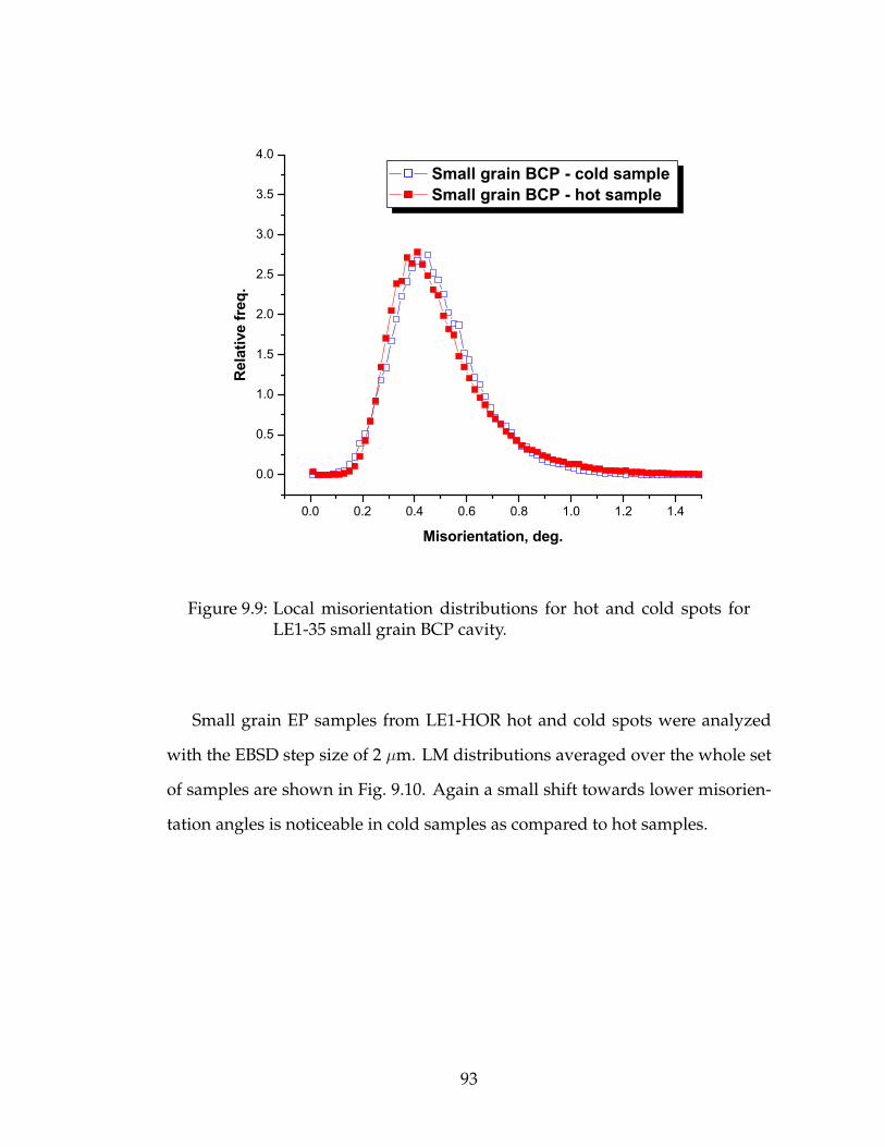
0.0 0.2 0.4 0.6 0.8 1.0 1.2 1.4
0.0
0.5
1.0
1.5
2.0
2.5
3.0
3.5
4.0
Rel
ativ
e fr
eq.
Misorientation, deg.
Small grain BCP - cold sample Small grain BCP - hot sample
Figure 9.9: Local misorientation distributions for hot and cold spots forLE1-35 small grain BCP cavity.
Small grain EP samples from LE1-HOR hot and cold spots were analyzed
with the EBSD step size of 2 µm. LM distributions averaged over the whole set
of samples are shown in Fig. 9.10. Again a small shift towards lower misorien-
tation angles is noticeable in cold samples as compared to hot samples.
93
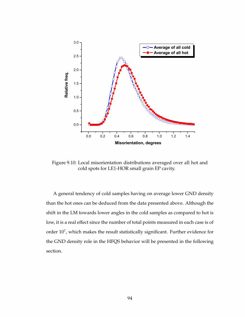
0.0 0.2 0.4 0.6 0.8 1.0 1.2 1.4
0.0
0.5
1.0
1.5
2.0
2.5
3.0
Rel
ativ
e fr
eq.
Misorientation, degrees
Average of all cold Average of all hot
Figure 9.10: Local misorientation distributions averaged over all hot andcold spots for LE1-HOR small grain EP cavity.
A general tendency of cold samples having on average lower GND density
than the hot ones can be deduced from the data presented above. Although the
shift in the LM towards lower angles in the cold samples as compared to hot is
low, it is a real effect since the number of total points measured in each case is of
order 107, which makes the result statistically significant. Further evidence for
the GND density role in the HFQS behavior will be presented in the following
section.
94

9.5 Baking effect on cavity samples
In order to study the effect of baking on dislocation density in hot and cold sam-
ples, several samples from all cavities, which had been dissected, were baked at
100-120 C for at least 48 hours.
In Fig. 9.11 the local misorientation distribution is shown before and after
UHV annealing at 110C for 48 hours for the hot sample from LE1-37 large grain
BCP cavity. EBSD orientation maps were obtained with a 2 µm step and LM
distributions were calculated from them. Baking resulted in the change of LM
distribution manifested in the reduced fraction of higher angle misorientations -
effectively the shift of the distribution towards lower angles. From Sec. 9.2.3 we
know that it corresponds to the reduced density of GNDs in the baked sample.
95
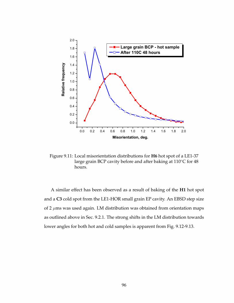
0.0 0.2 0.4 0.6 0.8 1.0 1.2 1.4 1.6 1.8 2.0
0.0
0.2
0.4
0.6
0.8
1.0
1.2
1.4
1.6
1.8
2.0
Rel
ativ
e fr
eque
ncy
Misorientation, deg.
Large grain BCP - hot sample After 110C 48 hours
Figure 9.11: Local misorientation distributions for H6 hot spot of a LE1-37large grain BCP cavity before and after baking at 110C for 48hours.
A similar effect has been observed as a result of baking of the H1 hot spot
and a C3 cold spot from the LE1-HOR small grain EP cavity. An EBSD step size
of 2 µms was used again. LM distribution was obtained from orientation maps
as outlined above in Sec. 9.2.1. The strong shifts in the LM distribution towards
lower angles for both hot and cold samples is apparent from Fig. 9.12-9.13.
96

0.0 0.2 0.4 0.6 0.8 1.0 1.2 1.4
0.0
0.5
1.0
1.5
2.0
2.5
3.0
3.5
4.0
Rel
ativ
e fr
eq.
Misorientation, deg.
Small grain EP - hot sample After 120C 40 hours
Figure 9.12: Local misorientation distributions for the H1 hot spot of aLE1-HOR small grain EP cavity before and after baking at120C for 40 hours.
97
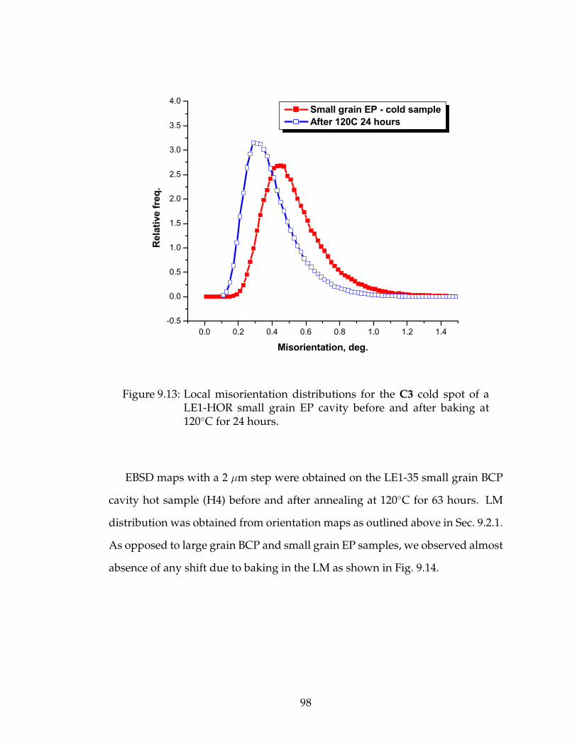
0.0 0.2 0.4 0.6 0.8 1.0 1.2 1.4-0.5
0.0
0.5
1.0
1.5
2.0
2.5
3.0
3.5
4.0
Rel
ativ
e fr
eq.
Misorientation, deg.
Small grain EP - cold sample After 120C 24 hours
Figure 9.13: Local misorientation distributions for the C3 cold spot of aLE1-HOR small grain EP cavity before and after baking at120C for 24 hours.
EBSD maps with a 2 µm step were obtained on the LE1-35 small grain BCP
cavity hot sample (H4) before and after annealing at 120C for 63 hours. LM
distribution was obtained from orientation maps as outlined above in Sec. 9.2.1.
As opposed to large grain BCP and small grain EP samples, we observed almost
absence of any shift due to baking in the LM as shown in Fig. 9.14.
98
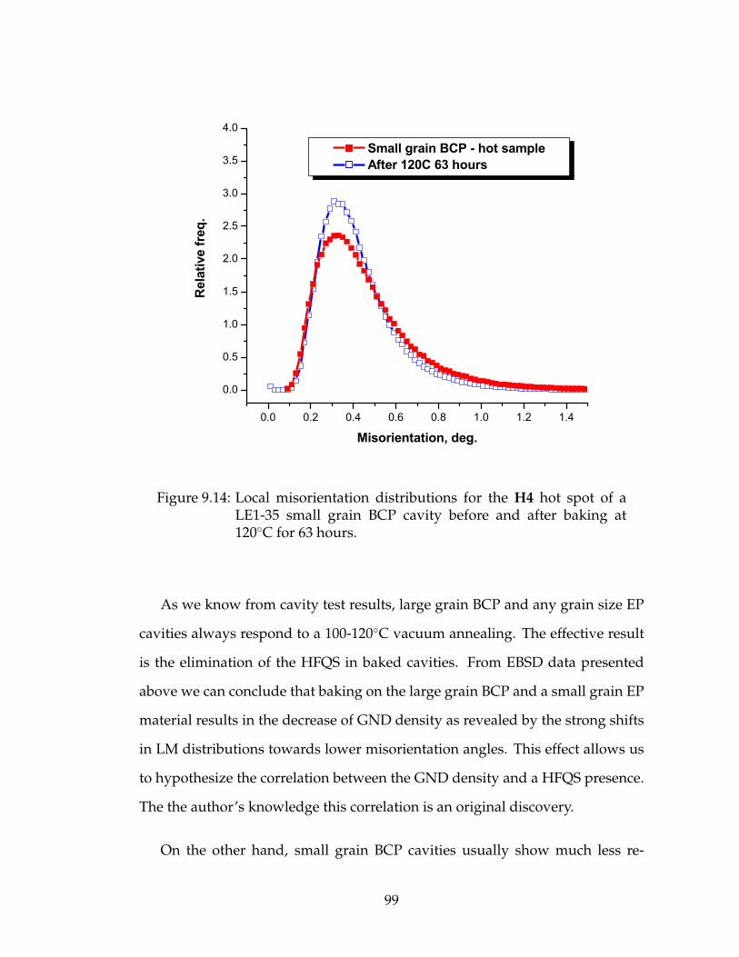
0.0 0.2 0.4 0.6 0.8 1.0 1.2 1.4
0.0
0.5
1.0
1.5
2.0
2.5
3.0
3.5
4.0
Rel
ativ
e fr
eq.
Misorientation, deg.
Small grain BCP - hot sample After 120C 63 hours
Figure 9.14: Local misorientation distributions for the H4 hot spot of aLE1-35 small grain BCP cavity before and after baking at120C for 63 hours.
As we know from cavity test results, large grain BCP and any grain size EP
cavities always respond to a 100-120C vacuum annealing. The effective result
is the elimination of the HFQS in baked cavities. From EBSD data presented
above we can conclude that baking on the large grain BCP and a small grain EP
material results in the decrease of GND density as revealed by the strong shifts
in LM distributions towards lower misorientation angles. This effect allows us
to hypothesize the correlation between the GND density and a HFQS presence.
The the author’s knowledge this correlation is an original discovery.
On the other hand, small grain BCP cavities usually show much less re-
99
sponse to the mild baking than do large grain and EP-treated cavities. And
our EBSD studies on the small grain BCP hot spots showed that in fact the effect
of baking is almost not present. This is a compelling correlation, which adds
strength to our hypothesis, which is going to be considered in more detail in the
following chapter.
100
CHAPTER 10
POSSIBLE MECHANISMS FOR THE HFQS AND THE MILD BAKING
EFFECT
10.1 Introduction
In this chapter we propose a model for the HFQS than also explains the follow-
ing effects due to baking:
1. Baking has a large effect on EP cavities
2. Baking has a large effect on large grain cavities
3. The depth of baking benefit is 10-20 nm
EBSD studies of the samples from three different cavities considered in
Chapter 9 allow us to propose a possible model for the observed HFQS heat-
ing patterns and the 100-120C annealing effect.
We suggest that the underlying cause of the observed heating non-
uniformity might be the difference in plastic deformation – hot areas have a
larger Geometrically Necessary Dislocation (GND) density than the cold ones.
Higher GND density results in a locally suppressed Bean-Livingston barrier
due to vortex attraction to dislocations (pinning force) as shown, for example,
in [30, 5].
A possible explanation for the baking effect based on the dislocation climb
process is proposed.
101

10.2 Bean-Livingston surface barrier
Bean and Livingston [4] have theoretically deduced that on the surface of type II
superconductors there exists a potential barrier for the penetration of fluxoids.
They considered the forces acting on a fluxoid close to the surface of the type II
superconductor. Since the currents at the surface should have no perpendicular
component, this boundary condition results in the existence of an “image” force
acting on the fluxoid, which attracts it to the surface in full analogy to the force
of an image charge in electrostatics. Another force acting upon the fluxoid is
the force exerted by the external magnetic field, which pushes the fluxoid in-
side the superconductor. The image force and the magnetic force have different
dependencies on the distance from the surface and thus the surface barrier in
the fluxoid energy emerges. Bean and Livingston were able to calculate the sur-
face barrier for different magnitudes of the applied magnetic field as shown in
Fig. 10.1.
102

Figure 10.1: Dependence of the fluxoid line energy on distance fromthe surface for different applied magnetic fields (reproducedfrom [4]).
An existence of the surface barrier was subsequently experimentally demon-
strated. It was also found that the dislocation density has a dramatic effect on
the surface barrier. Hysteretic behavior in magnetization is determined by a
surface barrier and its change with the dislocation content is shown in Fig. 10.2,
103

which is reproduced from [29].
Figure 10.2: Effect of the subsequent room temperature annealing onthe lead-8.23 wt.% indium alloy. A–as-cold swaged, B–annealed 30 min, C–1 day, D–18 days, E–46 days (reproducedfrom [29]).
10.3 Dislocation-based model for the HFQS
There are many sources for producing dislocations in niobium for cavities. The
starting sheet material has dislocations due to rolling. Annealing for recrys-
tallization removes most, but possibly not all dislocations. Mechanical defor-
mation performed on niobium in order to form the elliptical cavity shape (i.e.
half-cell deep drawing or spinning) results in the high dislocation density intro-
duced inside the material in order to accommodate a plastic deformation. Since
applied stress is not uniform a surface deformation is higher than the bulk.
Subsequent chemical etching (i.e. BCP or EP) results in the removal of the
surface layer of a very high dislocation content (“damage” layer). On the other
104
hand, the dislocation structure left by chemical treatments in the surface layer
of niobium might be different from that in the bulk.
A high dislocation density lowers the energy of a single vortex inside nio-
bium due to the attractive interaction between a vortex and a dislocation (pin-
ning force), effectively reducing the Bean-Livingston surface barrier height.
Thus vortex penetration happens at lower RF fields in areas with the higher
dislocation density, manifesting itself in the higher dissipation due to the pres-
ence of the vortex core in the RF layer and due to the dissipative oscillatory
motion of vortices under the driving Lorentz force.
Variations of the dislocation density over the high-magnetic-field region of
cavity walls can produce the observed heating non-uniformity in the HFQS
regime as found by temperature mapping - see Fig. 6.4. Dislocation density after
baking is reduced in hot areas to the value below the density in the cold spots
before baking. Before baking both hot and cold areas have dislocation densities
high enough for the HFQS to appear everywhere but with the different strength
(hot and cold ares), as found by cavity tests with thermometry. After baking,
the dislocation density is reduced, so flux entry and losses become low.
The presence of fluxoids inside niobium within the RF magnetic field pene-
tration depth causes dissipation, which consists of two components:
• Inductive losses due to the stationary fluxoid normal conducting core orig-
inating from the superconducting current time variation
• Losses due to the fluxoid motion arising from the viscous drag
The dissipation mechanism due to vortex moving in and out of niobium
105
driven by a strong RF field have been recently theoretically studied by Gure-
vich and Ciovati in [26]. The losses due to viscous flux motion accompanied
by a flux pinning rise sharply for RF field amplitudes higher than the first flux-
entry field B v, which depends on the particular defect serving as a “gate” for
the flux entry. In another theoretical study a dissipation due to a single oscil-
lating vortex, which is already in the surface layer of a superconductor, was
considered by Rabinowitz in [39, 38].
The difference between models in [26] and [39, 38] is that the former model
does not take into account the effective mass of the fluxoid, whereas the latter
one neglects the image force acting on the fluxoid due to the presence of the
surface.
The experimental measurements of the velocity of the magnetic field pen-
etration in niobium reported in [21] give at 4.2 K the value of vp = 3100 −4700 cm/s. Contrary to the common belief within the SRF community, this speed
does not translate into the fluxoid nucleation time much larger than the RF pe-
riod for all fluxoids. The nucleation times for the fluxoids parallel and perpen-
dicular to the cavity surface are significantly different due to the distance the
magnetic field should travel in each case. For the case of a d = 3 mm cavity
wall thickness the nucleation time for the fluxoid perpendicular to the surface
is τ⊥ = d/vp ≈ 10−6 sec, but for the fluxoid parallel to the surface the magnetic
field only has to travel about the coherence length ξ = 40 nm, and that gives
τ‖ = ξ/vp ≈ 10−9 sec, which is of the same order of magnitude as the RF period
for 1.5 GHz cavities.
We will follow the simplified model of Rabinowitz to estimate the fluxoid-
related losses in the case of niobium cavities, reproduced here for understanding
106

the losses. The schematic of the problem in hand is shown in Fig. 10.3.
Figure 10.3: Schematic of the single fluxoid within the London penetrationdepth of the niobium surface with the forces acting on it in theRabinowitz’s model [39, 38].
Following Rabinowitz we first estimate the inductive losses due to the sta-
tionary normal conducting core. The electric field induced in a superconductor
by the variable current is:
E =m
e
[1
ne
dj
dt
]=
imω
ne2j = ρsj (10.1)
where ρs is the superconducting electrical resistivity. Under the assumption that
the induced electric field is approximately uniform throughout the fluxoid core,
the average dissipated power per unit volume in the normal conducting core is:
dP
dV=
1
2ρ′nE2 (10.2)
107

where ρ′n is the effective resistivity of the stationary normal region if the actual
current flowing through it is used.
ρ′n = Gρn, G ≥ 1 (10.3)
The value of G depends on the relative magnitudes of the electron mean free
path and the radius of the fluxoid and for niobium it is close to G=1. Using
Eq. (10.1) together with Eq. (10.2) we obtain:
dP
dV=
1
2
(ρ2
s
ρ′n
)j20 =
1
2ρstatj
20 (10.4)
where
ρstat =ρ2
s
ρ′n=
m2ω2
n2e4G
1
ρn
(10.5)
is the effective resistivity of the normal region if the supercurrent is to flow
through it. For niobium cavities at 1.5 GHz we obtain ρstat ≈ 3.6 × 10⁻¹⁴Ω · mand the effective surface resistance of Rstat = ρstat
2πλ≈ 0.14µΩ for a single normal
core.
If the fluxoid is not stationary but moving inside the superconductor, an ad-
ditional dissipation arises. The mechanism of this additional dissipation can be
simply explained by the additional electric field induced by the moving mag-
netic flux. This induced electric field acts on the normal electrons within the
fluxoid core causing the dissipation.
Now, let’s consider the forces acting on the fluxoid inside a superconduc-
tor. As mentioned above, the image force is neglected in this model and
there are three forces, which act on the fluxoid - a driving Lorentz force FL =
Re[φ0j0exp(iωt)], a viscous drag force ηv(t), and a pinning force fp = −pX(t).
Thus the equation of motion for the fluxoid has the form:
MX ′′(t) + ηX ′(t) + pX(t) = Re[φ0j0exp(iωt)] (10.6)
108

The solution of Eq. (10.6) is
X(t) = ReX0exp[i(ωt + δ)] (10.7)
For the fluxoid, which is not stationary but oscillating under the influence of
the Lorentz force, the power dissipation per unit volume is determined by the
work of the Lorentz force averaged over time:
dP
dV=
1
2Re
[j× µH ·
(dXdt
)]=
1
2ρeffj
20 (10.8)
where j0 is the superconducting current density at the surface of the super-
conductor and ρeff is the effective resistivity of the oscillating fluxoid. Using
Eq. (10.7) we obtain the effective resistivity for the case of the fluxoid parallel to
the surface to be:
ρeff =ω2φ2HH0µ
2
ρ2n(ω2M − p) + ω2φ2H2
0µ2ρn (10.9)
where φ is a total magnetic flux in the fluxoid, M is the effective mass of the
fluxoid per unit length, p is the pinning force per unit length of the fluxoid, ρn
is a normal state resistivity, H is the magnetic field in the fluxoid, and H0 = Hc2
- upper critical field.
The effective mass of the fluxoid M is given by the Bardeen-Stephen for-
mula [3]:
M = 2πnma2
(H0
H
)2
sin2α (10.10)
where n is the electron density, m is the electron mass, a is the radius of the
fluxoid, and α is a Hall angle.
Substituting Eq. (10.10) into Eq. (10.9) we obtain for the general case:
ρeff =ω2φ2HH0µ
2
ρ2n
(2πω2nma2
(H0
H
)2sin2α− p
)2
+ ω2φ2H20µ
2
ρn (10.11)
109

To estimate the mass per unit length of a single quantum of magnetic flux
φ0 we assume that sin2α = 1, a ≈ ξ ≈ 40 nm, n = 5.55 × 1028 m−3, H = H0 =
400 mT ≈ 3.2× 10⁵ Am
to obtain:
M ≈ 5.1× 10⁻¹⁶ kg (10.12)
Since the pinning force p per unit length of the fluxoid is not known, we will
use the approximation of p ¿ ω2M first and will discuss the effect of a non-
negligible p later. Using the value of ρn ≈ 10−9 Ω ·m for Nb at low temperatures
we obtain:
ρeff ≈ 2.9× 10⁻¹¹Ω ·m (10.13)
and the effective surface resistance is
Rosc =ρeff
2πλ≈ 120µΩ (10.14)
The surface resistance due to the stationary normal conducting core is there-
fore much less than the surface resistance due to the oscillatory motion of the
fluxoid. The total surface resistance of the single oscillating fluxoid is thus:
Rfluxs = Rstat + Rosc ≈ 120µΩ (10.15)
First we estimate the needed number of fluxoids Nflux to produce losses,
which are comparable to the power dissipation due to regular BCS losses for
the ideal cavity. We assume that the effective area of each oscillating fluxoid is
πξ2 and then we obtain for the power of the fluxoid-related losses:
Pflux =1
2Rflux
s AfluxH2 (10.16)
where Aflux = Nfluxπξ2 - total effective area of the oscillating fluxoids. For the
regular BCS losses we have:
Pdiss =1
2RBCS
s AcavH2 (10.17)
110

where Acav is the effective area of the cavity, Acav ≈ 0.156 m2, and RBCSs ≈
13.8 nΩ at Q0 = 2× 10¹⁰.
If Pflux is equal to Pdiss than the Q0 of the cavity will decrease by a factor of 2.
From Eq. (10.16) and 10.17 we obtain:
1
2Rflux
s Aflux =1
2RBCS
s Acav ⇒ σflux =Nflux
Acav
=1
Aflux
RBCSs
Rfluxs
≈ 1.7× 10¹⁰ m−2
where σflux is the area density of fluxoids required to decrease the Q0 by a factor
of 2. This density of fluxoids corresponds to the average spacing between the
fluxoids to be:
l ≈ 1√σflux
= 8 µm
If we compare the fluxoid density with the value obtained from the disloca-
tion density tensor calculations based on EBSD data for the H6 sample from a
large grain LE1-37 cavity (Fig. 9.5), the estimate for σflux is about three orders of
magnitude lower than the estimated dislocation density. There are two possible
explanations for the difference.
First one is that if we assume that there is only some fraction of disloca-
tions, which have types and/or orientations with respect to the applied mag-
netic field, favorable for the earlier flux entry in the form of single oscillating
fluxoids at each dislocation center, then the difference might come from the fact
that not all dislocations will serve as flux entry sites initially, but as the ap-
plied magnetic field increases, more and more fluxoids penetrate, increasing
the losses until the quench is reached at some location.
Another explanation comes from the finding that dislocations in a cavity-
grade niobium are distributed non-uniformly and form a dislocation cell struc-
ture. In this structure the dislocation density is much higher in the dislocation
111
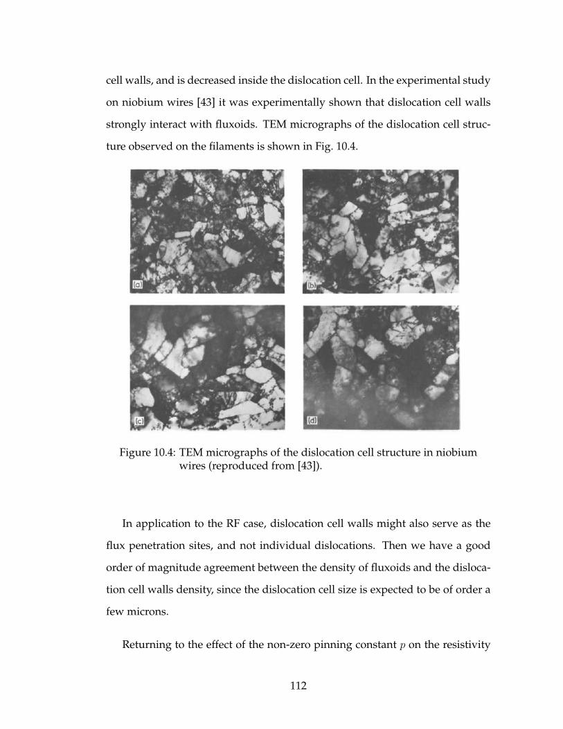
cell walls, and is decreased inside the dislocation cell. In the experimental study
on niobium wires [43] it was experimentally shown that dislocation cell walls
strongly interact with fluxoids. TEM micrographs of the dislocation cell struc-
ture observed on the filaments is shown in Fig. 10.4.
Figure 10.4: TEM micrographs of the dislocation cell structure in niobiumwires (reproduced from [43]).
In application to the RF case, dislocation cell walls might also serve as the
flux penetration sites, and not individual dislocations. Then we have a good
order of magnitude agreement between the density of fluxoids and the disloca-
tion cell walls density, since the dislocation cell size is expected to be of order a
few microns.
Returning to the effect of the non-zero pinning constant p on the resistivity
112
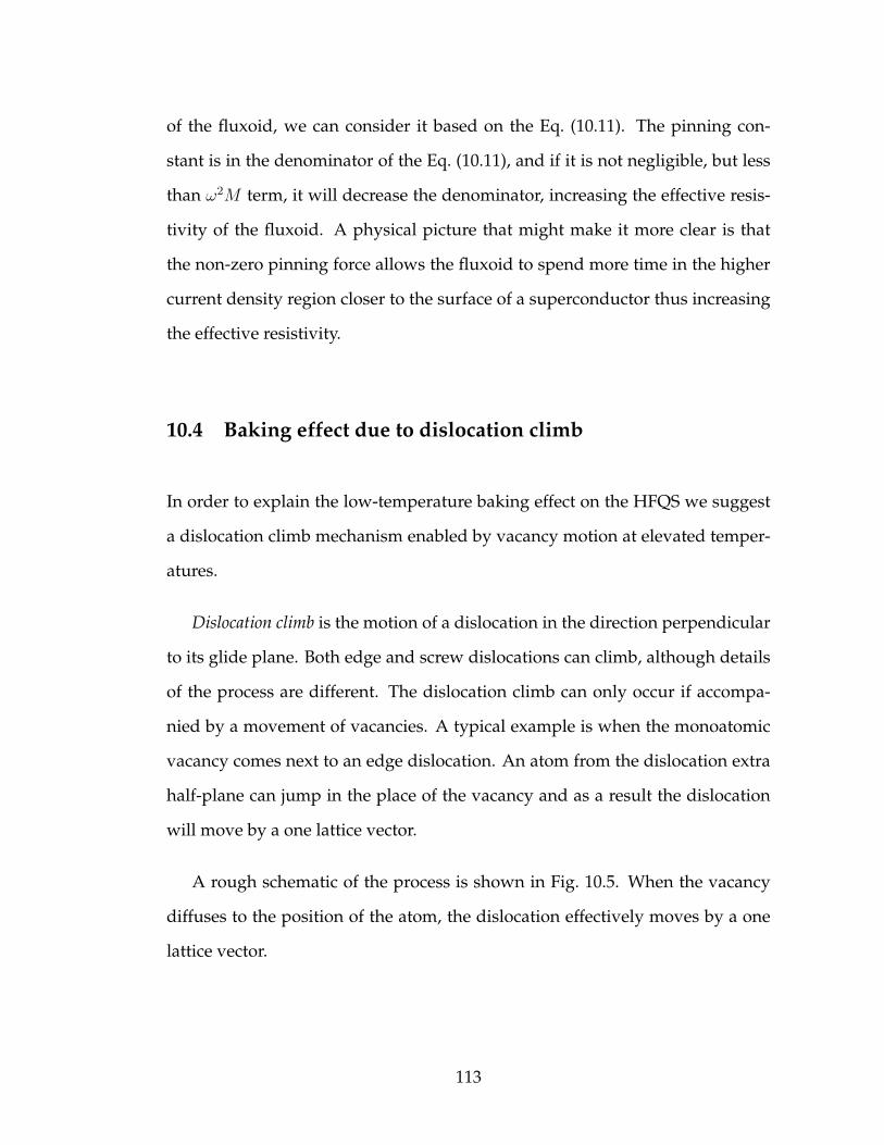
of the fluxoid, we can consider it based on the Eq. (10.11). The pinning con-
stant is in the denominator of the Eq. (10.11), and if it is not negligible, but less
than ω2M term, it will decrease the denominator, increasing the effective resis-
tivity of the fluxoid. A physical picture that might make it more clear is that
the non-zero pinning force allows the fluxoid to spend more time in the higher
current density region closer to the surface of a superconductor thus increasing
the effective resistivity.
10.4 Baking effect due to dislocation climb
In order to explain the low-temperature baking effect on the HFQS we suggest
a dislocation climb mechanism enabled by vacancy motion at elevated temper-
atures.
Dislocation climb is the motion of a dislocation in the direction perpendicular
to its glide plane. Both edge and screw dislocations can climb, although details
of the process are different. The dislocation climb can only occur if accompa-
nied by a movement of vacancies. A typical example is when the monoatomic
vacancy comes next to an edge dislocation. An atom from the dislocation extra
half-plane can jump in the place of the vacancy and as a result the dislocation
will move by a one lattice vector.
A rough schematic of the process is shown in Fig. 10.5. When the vacancy
diffuses to the position of the atom, the dislocation effectively moves by a one
lattice vector.
113

Figure 10.5: Schematic of the edge dislocation climb through vacancy dif-fusion.
The dislocation climb process has a strong temperature dependence as op-
posed to another form of dislocation movement – slip. Since cavity experiments
suggest that the HFQS has a strong response to the temperature of baking, it
points toward dislocation climb as a possible mechanism for the baking effect.
The temperature dependence of the dislocation climb comes from the strong
link between the climb and vacancies, which have a strongly temperature de-
pendent diffusion coefficient:
D = D0e− Ea
kbT (10.18)
where Ea is the activation energy. The value of Ea for niobium is not found in
the literature, but positron annihilation studies show [13] that at about 100C va-
cancies become mobile due to the dissociation of vacancy-hydrogen complexes,
which bind vacancies and prevent them from moving. So baking turns on the
dislocation climb mechanism by freeing the vacancies. It should be noted that
the concentration of vacancies should not necessarily change as a result of bak-
ing, since the role of vacancies is to just provide a mechanism for the dislocation
motion. Some preliminary positron annihilation studies were performed in or-
der to study the effect of mild baking on the vacancy concentration, these are
reported in Appendix A.
114
The net result of the 100-120C baking is a decreased number of dislocations
in the London penetration depth, which translates into a smaller number of
sites for a premature flux entry. Baking may particularly reduce the number of
dislocations, which are oriented favorably for the magnetic flux to enter at low
field levels.
The fact that small grain cavities require longer baking times as compared to
large grain and single grain cavities can also be explained by the effect of grain
boundaries on the annealing, grain boundaries being the obstacles in the way
of dislocation and vacancy motion during the baking.
Small grain BCP cavities often do not respond to the baking as found by
cavity tests, so that the HFQS is not removed. Since surface irregularities (i.e.
GBs) have sharper and deeper steps, the total roughness is much higher for
the BCP surface. This prevents the motion of dislocations required for the total
“healing” effect of baking.
The destructive effect of more than about 20 nm material removal by anodiz-
ing [10] or BCP or EP on the baking benefit might come from the fact that only
material within the dislocation climb range is modified by baking, since dislo-
cations can climb out of niobium only at the surface and the bulk dislocation
density is not affected. Chemical treatment thus just removes the layer, which
was modified and restores the bulk dislocation concentration.
To summarize, we suggest that vacancies in niobium, which become mobile
starting at about 100C, enable dislocations to climb out of niobium, which re-
sults in the reduced dislocation density in the surface layer. As a result there are
fewer flux quanta present in the penetration depth and smaller losses.
115

CHAPTER 11
SUMMARY
Surface characterization of the hot and cold areas dissected from niobium cav-
ities of different grain size, which had BCP and EP treatment prior to test, al-
lowed to make several conclusions about the role of different surface properties
in the HFQS.
A roughness of hot and cold samples was analyzed by optical profilometry
and was found to be the same on all relevant scales. Therefore it cannot be
responsible for the heating patterns in the HFQS regime, and, perhaps, can be
eliminated from the list of primary causes of the HFQS as well.
A niobium oxide structure of hot and cold samples was analyzed using XPS.
Results show that the oxide structure is very similar for all samples analyzed, at
least at the level of XPS sensitivity (0.1-1 at.%). Hence, differences in the oxide
cannot be the underlying cause of the HFQS heating non-uniformity.
Nitrogen was identified as a possible contributor to the heating patchiness
in the small grain BCP case, as three hottest samples exhibited a significant ni-
trogen signal. Still, small grain EP and large grain BCP cavities did not have any
excess nitrogen in the hot areas. Thus, a full role of common contaminants (C,
N) is not completely clear, but most likely they play a minor role in the HFQS if
any.
Grain orientations have been analyzed on the small grain BCP hot and cold
samples and it was shown that the texture is random and there is no preferential
orientation present.
116

A difference in the dislocation structure of hot and cold samples found by
EBSD was identified as a possible source of the HFQS heating non-uniformity.
A change in the dislocation structure due to mild baking of cavity samples
was observed by EBSD.
An alternative explanation for the HFQS was proposed based on the prema-
ture flux penetration at dislocations or dislocation cell walls.
A possible mechanism for the mild baking effect based on the dislocation
climb enabled by vacancies was proposed.
117
APPENDIX A
POSITRON ANNIHILATION STUDIES
Vacancy concentration and mobility in niobium might play a role in the low
temperature baking effect, since vacancies can provide a mechanism for the
dislocation motion through a dislocation climb. In order to study the near-
surface concentration of vacancies and its change upon low temperature baking,
Positron Annihilation Spectroscopy (PAS) was used. PAS is based on the trapping
of positrons by the open volumes within the sample material followed by the
annihilation with electrons. The energy of the resulting γ-quanta depends on
the momentum of the electrons. The momentum of the electron in the annihila-
tion process is dependent upon whether the electron is in the regular lattice or
in the vacancy-like defect. As a result, a Doppler-broadening of the spectrum
of the produced radiation can be used as a measure of the distribution of elec-
tron momenta and thus the vacancy concentration. A detailed description of
the technique is beyond this thesis and can be found elsewhere.
Output data from PAS is the dependence of the so-called S-parameter on the
positron energy. S-parameter characterizes a sharpness of the X-ray spectrum,
and qualitatively the higher the S-parameter, the higher the vacancy concentra-
tion.
The energy of positrons Ep determines the depth d inside the material they
penetrate, and the approximate relation exists:
d[nm] =40
ρE1.6
p (A.1)
where ρ is the density in g/cm3 of the analyzed material.
118
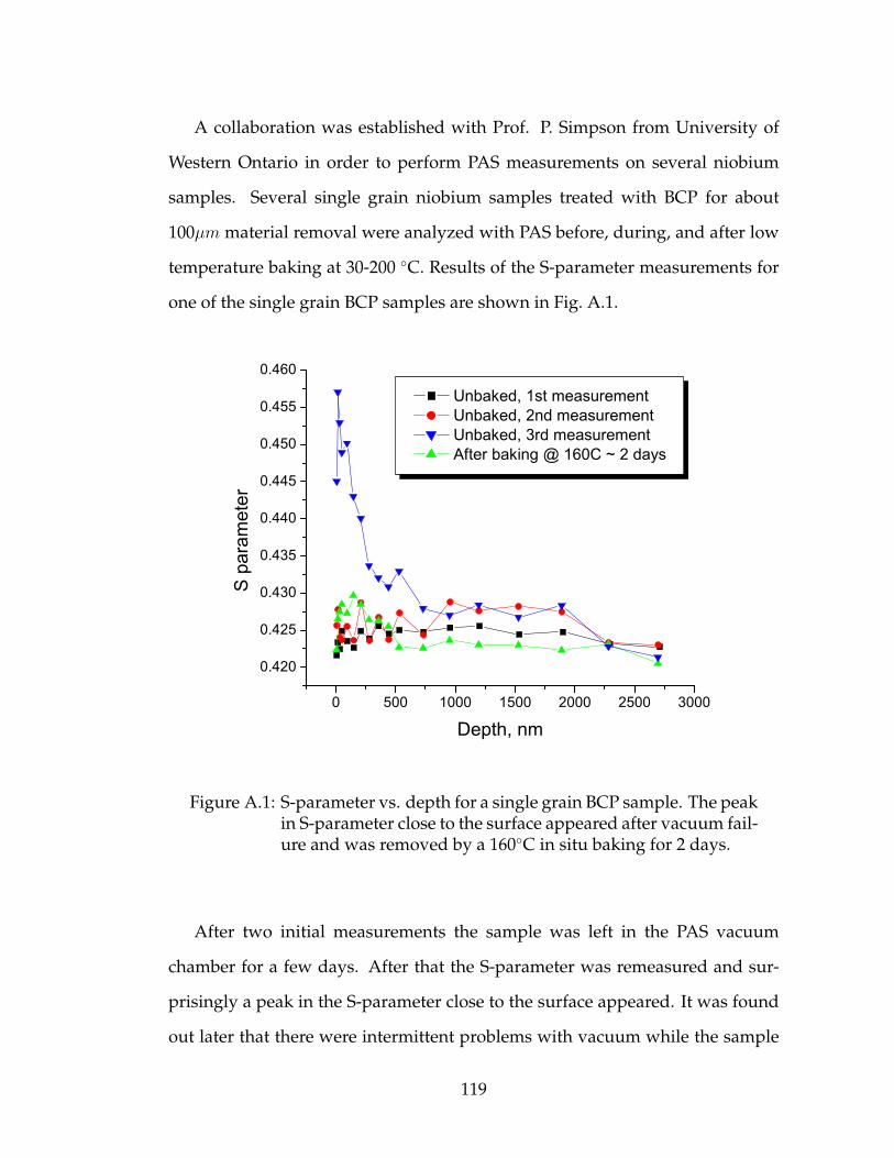
A collaboration was established with Prof. P. Simpson from University of
Western Ontario in order to perform PAS measurements on several niobium
samples. Several single grain niobium samples treated with BCP for about
100µm material removal were analyzed with PAS before, during, and after low
temperature baking at 30-200 C. Results of the S-parameter measurements for
one of the single grain BCP samples are shown in Fig. A.1.
0 500 1000 1500 2000 2500 3000
0.420
0.425
0.430
0.435
0.440
0.445
0.450
0.455
0.460
Unbaked, 1st measurement Unbaked, 2nd measurement Unbaked, 3rd measurement After baking @ 160C ~ 2 days
S p
aram
eter
Depth, nm
Figure A.1: S-parameter vs. depth for a single grain BCP sample. The peakin S-parameter close to the surface appeared after vacuum fail-ure and was removed by a 160C in situ baking for 2 days.
After two initial measurements the sample was left in the PAS vacuum
chamber for a few days. After that the S-parameter was remeasured and sur-
prisingly a peak in the S-parameter close to the surface appeared. It was found
out later that there were intermittent problems with vacuum while the sample
119

was sitting in the chamber, so that a vacuum failure caused the peak. It is un-
clear at this point if the peak corresponds to the increased vacancy density in the
surface layer or is a consequence of the adsorbed layer of residual gases released
during the pump failure (H, CO). Subsequent baking of the sample at 160C for
2 days and remeasuring the S-parameter showed that the peak was removed.
It was decided to ramp-anneal another sample (with the peak in S-
parameter) in vacuum by gradually increasing the temperature from room tem-
perature up to about 200C keeping the sample at each temperature in the pro-
cess for about 30 minutes, while investigating the S-parameter at Ep = 6 keV ,
which corresponds to the depth of about 20 nm in niobium. The results are
shown in Fig. A.2.
120
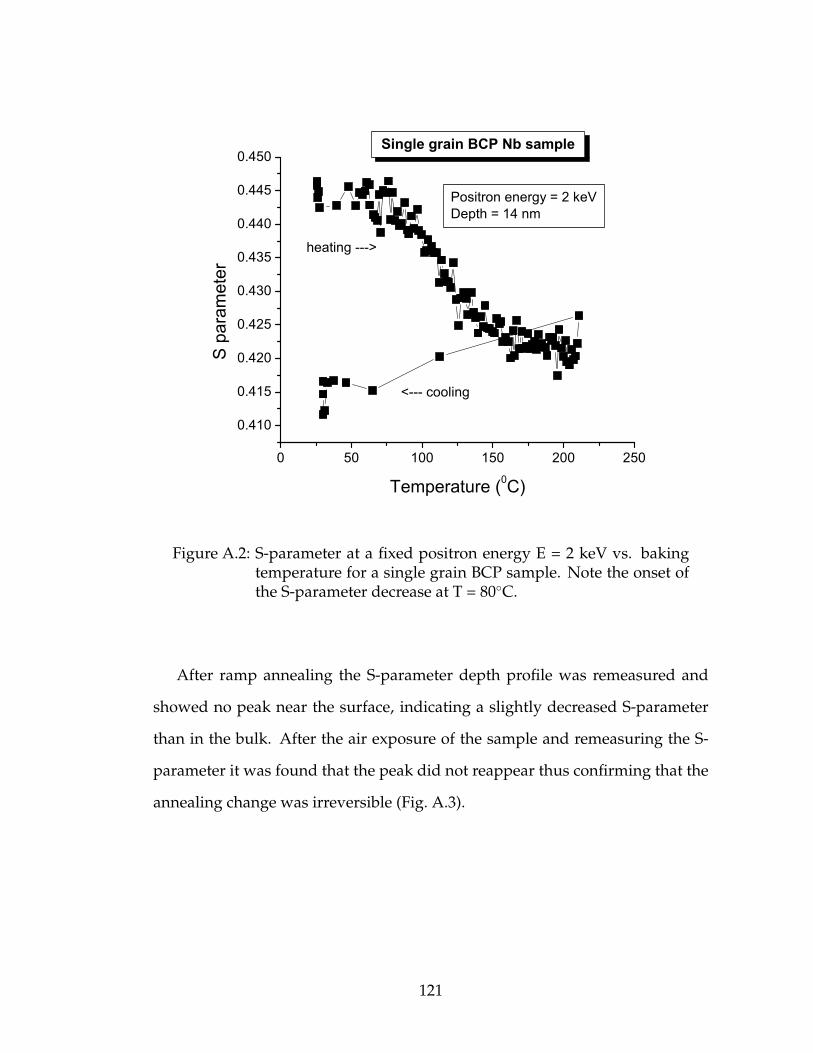
0 50 100 150 200 250
0.410
0.415
0.420
0.425
0.430
0.435
0.440
0.445
0.450
Positron energy = 2 keVDepth = 14 nm
Single grain BCP Nb sample
<--- cooling
heating --->
S p
aram
eter
Temperature (0C)
Figure A.2: S-parameter at a fixed positron energy E = 2 keV vs. bakingtemperature for a single grain BCP sample. Note the onset ofthe S-parameter decrease at T = 80C.
After ramp annealing the S-parameter depth profile was remeasured and
showed no peak near the surface, indicating a slightly decreased S-parameter
than in the bulk. After the air exposure of the sample and remeasuring the S-
parameter it was found that the peak did not reappear thus confirming that the
annealing change was irreversible (Fig. A.3).
121
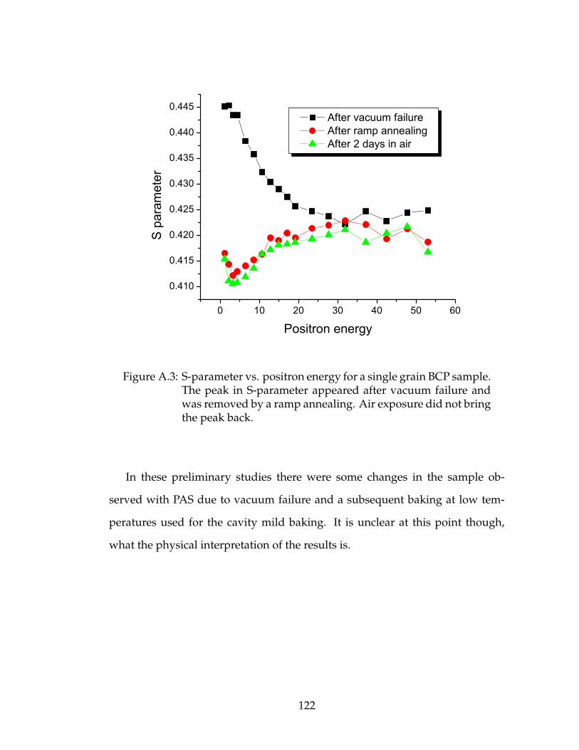
0 10 20 30 40 50 60
0.410
0.415
0.420
0.425
0.430
0.435
0.440
0.445
S p
aram
eter
Positron energy
After vacuum failure After ramp annealing After 2 days in air
Figure A.3: S-parameter vs. positron energy for a single grain BCP sample.The peak in S-parameter appeared after vacuum failure andwas removed by a ramp annealing. Air exposure did not bringthe peak back.
In these preliminary studies there were some changes in the sample ob-
served with PAS due to vacuum failure and a subsequent baking at low tem-
peratures used for the cavity mild baking. It is unclear at this point though,
what the physical interpretation of the results is.
122

BIBLIOGRAPHY
[1] C. Y. Ang. Acta Metall., 1:123, 1958.
[2] J. Bardeen, L. N. Cooper, and J. R. Schrieffer. Phys. Rev., 108:1175, 1957.
[3] J. Bardeen and M. J. Stephen. Phys. Rev., 140(A1197), 1965.
[4] C. Bean and J. D. Livingston. Phys. Rev. Lett., 12:86–87, 1964.
[5] A. M. Campbell and J. E. Evetts. Flux vortices and transport currents intype ii superconductors. Advances in Physics, 50(8):1249–1449, 2001.
[6] G. Ciovati. In Proceedings of the 11th Workshop on RF Superconductivity, 2005.
[7] G. Ciovati. PhD thesis, Old Dominion University, 2005.
[8] G. Ciovati. Improved oxygen diffusion model to explain the effect of low-temperature baking on high field losses in niobium superconducting cavi-ties. Appl. Phys. Lett., 89:022507, 2006.
[9] G. Eremeev. PhD thesis, Cornell University, 2008.
[10] G. Eremeev and H. Padamsee. Change in high field q-slope by anodizingof the baked cavity. Physica C, 441:134–136, 2006.
[11] G. Eremeev and H. Padamsee. Temperature map studies on nearly oxide-free, thin-oxide and standard-oxide cavities. In Proceedings of the 12th Work-shop on RF Superconductivity, 2007.
[12] H. Tian et al. Recent xps studies of the effect of processing on nb srf sur-faces. In Proceedings of the 13th Workshop on RF Superconductivity, 2007.
[13] J. Cizek et al. Phys. Rev. B, 32(7):4326–4331, 1985.
[14] J. Knobloch et al. High field q-slope in superconducting cavities due tomagnetic field enhancement at grain boundaries. In Proceedings of the 9thWorkshop on RF Superconductivity, 1999.
[15] J. Vines et al. Systematic trends for the medium field q-slope. In Proceedingsof the 13th Workshop on RF Superconductivity, 2007.
123

[16] R. L. Geng et al. Microstructures of rf surfaces in the electron-beam-weldregions of niobium. In Proceedings of the 9th Workshop on RF Superconductiv-ity, 1999.
[17] R. L. Geng et al. In Proceedings of PAC2007, 2007.
[18] T. Hays et al. In Proceedings of the 7th Workshop on RF Superconductivity, page437, 1995.
[19] T. Proslier et al. Tunneling study of cavity grade nb: possible magneticscattering at the surface. Appl. Phys. Lett., 92:212505, 2008.
[20] R. Fertig. PhD thesis, Cornell University, 2008.
[21] R. B. Flippen. The radial velocity of magnetic field penetration in type iisuperconductors. Phys. Lett., 17(3), 1965.
[22] R. H. Fowler and L. Nordheim. Proc. R. Soc. Lond. A, Math. Phys. Sci.,119:173, 1928.
[23] R. A. French. Cryogenics, 8:301, 1968.
[24] V. L. Ginzburg and L. D. Landau. Zh. Eksp. Teor. Fiz. [Sov. Phys. - JETP],20:1064, 1950.
[25] A. Gurevich. Thermal rf breakdown of superconducting cavities. In Pro-ceedings of the Workshop on Pushing the Limits of RF Superconductivity., 2005.
[26] A. Gurevich and G. Ciovati. Dynamics of vortex penetration, jumpwiseinstabilities, and nonlinear surface resistance of type-ii superconductors instrong rf fields. Physical Review B, 77:104501, 2008.
[27] J. Halbritter. Degradation of superconducting rf cavity performances byextrinsic properties. In Proceedings of the 10th Workshop on RF Superconduc-tivity, 2003.
[28] J. Knobloch. PhD thesis, Cornell University, 1997.
[29] J. D. Livingston. Phys. Rev., 129:1943, 1963.
[30] J. D. Livingston. Defects and magnetic hysteresis in type ii superconduc-tors. Rev. Mod. Phys., 36(1):54–58, Jan 1964.
124

[31] M. H. Matloob and M. W. Roberts. J. Chem. Soc., Faraday Trans. 1, 73:1393–1405, 1977.
[32] P. E. Mix. Introduction to Nondestructive Testing: A Training Guide. Wiley-IEEE, 2005.
[33] J. F. Nye. Some geometrical relations in dislocated crystals. Acta Metall.,1:153–162, 1953.
[34] E. Orowan. Z. Phys., 89, 1934.
[35] H. Padamsee, J. Knobloch, and T. Hays. RF Superconductivity for Accelera-tors. John Wiley and Sons, 1998.
[36] W. Pantleon. Resolving the geometrically necessary dislocation content byconventional electron backscattering diffraction. Scripta Materialia, 58:994–997, 2008.
[37] M. Polanyi. Z. Phys., 89, 1934.
[38] M. Rabinowitz. Appl. Phys. Lett., 19(73), 1971.
[39] M. Rabinowitz. Analysis of a critical loss in a superconductor. J. Appl. Phys.,88(42), 1971.
[40] A. Romanenko. Review of high field q-slope, surface measurements. InProceedings of the 12th Workshop on RF Superconductivity., 2007.
[41] H. Safa. In Proceedings or the 9th Workshop on RF Superconductivity, 1999.
[42] D. Saint-James and P. G. De Gennes. Phys. Lett., 7:306–308, 1963.
[43] A. T. Santhanam. Journal of Materials Science, 11:1099–1102, 1976.
[44] A. J. Schwartz, M. Kumar, and B. L. Adams, editors. Electron BackscatterDiffraction in Materials Science. Kluwer Academic/Plenum Publishers, 2000.
[45] G. I. Taylor. Proc. R. Soc. London, 145A, 1934.
[46] H. Tian. Scale-specific nb surface topographic characterizations for super-conducting rf accelerators cavities. In Proceedings of the 3rd International
125

Workshop on Thin films and New Ideas for pushing the limits of RF Superconduc-tivity, 2008.
[47] B. Visentin. In Proceedings of the Workshop on Pushing the Limits of RF Super-conductivity, 2006.
126