switch-mode power converters - · pdf fileswitch-mode power converters ... switching power...
TRANSCRIPT

Switch-Mode Power Converters

This page intentionally left blank

Switch-Mode Power Converters
Design and Analysis
Keng C. Wu
Amsterdam • Boston • Heidelberg • London • New York • OxfordParis • San Diego • San Francisco • Singapore • Sydney • Tokyo

Elsevier Academic Press
30 Corporate Drive, Suite 400, Burlington, MA 01803, USA
525 B Street, Suite 1900, San Diego, California 92101-4495, USA
84 Theobald’s Road, London WC1X 8RR, UK
This book is printed on acid-free paper.
Copyright � 2006, Elsevier Inc. All rights reserved.
No part of this publication may be reproduced or transmitted in any form or by any
means, electronic or mechanical, including photocopy, recording, or any information
storage and retrieval system, without permission in writing from the publisher.
Permissions may be sought directly from Elsevier’s Science & Technology Rights
Department in Oxford, UK: phone: (þ44) 1865 843830, fax: (þ44) 1865 853333,
e-mail: [email protected]. You may also complete your request on-line via
the Elsevier homepage (http://elsevier.com), by selecting ‘‘Customer Support’’ and
then ‘‘Obtaining Permissions.’’
Library of Congress Cataloging-in-Publication Data
Wu, Keng C., 1948-
Switch-mode power converters / Keng C. Wu.
p. cm.
Includes bibliographical references and index.
ISBN 0-12-088795-9 (alk. paper)
1. Electric current converters. 2. Switching power supplies. I. Title.
TK7872.C8W853 2006
621.31’7–dc22
2005014319
British Library Cataloguing in Publication Data
A catalogue record for this book is available from the British Library
For information on all Academic Press publications visit our Web site at
www.academicpress.com
Printed in the United States of America
05 06 07 08 09 9 8 7 6 5 4 3 2 1

To
My wife, Shwu
My daughter, Stephanie
My mother, Tai

This page intentionally left blank

Table of Contents
Preface. . . . . . . . . . . . . . . . . . . . . . . . . . . . . . . . . . . . . . . . . xiii
1. Isolated Step-Down (Buck) Converter 1
1.1. CCM Open-Loop Output and Duty Cycle
Determination. . . . . . . . . . . . . . . . . . . . . . . . . . . . . . . . 1
1.2. DCM Open-Loop Output and Duty Cycle
Determination. . . . . . . . . . . . . . . . . . . . . . . . . . . . . . . . 5
1.3. CCM to DCM Transition, Critical Inductance . . . . . . . . . . 6
1.4. Gain Formula for Nonideal Operational Amplifiers . . . . . . 7
1.5. Feedback under Voltage-Mode Control. . . . . . . . . . . . . . . 9
1.6. Voltage-Mode CCM Closed Loop . . . . . . . . . . . . . . . . . . 11
1.7. Voltage-Mode DCM Closed Loop . . . . . . . . . . . . . . . . . . 13
1.8. Voltage-Mode CCM Small-Signal Stability . . . . . . . . . . . . 14
1.9. Current-Mode Control . . . . . . . . . . . . . . . . . . . . . . . . . . 19
1.10. CCM Current-Mode Control in a Closed-Loop
Steady State . . . . . . . . . . . . . . . . . . . . . . . . . . . . . . . . . 21
1.11. CCM Current-Mode Control Small-Signal Stability. . . . . . . 24
1.12. Output Capacitor Size and Accelerated Steady-State
Analysis . . . . . . . . . . . . . . . . . . . . . . . . . . . . . . . . . . . . 26
1.13. A Complete Example . . . . . . . . . . . . . . . . . . . . . . . . . . . 33
1.14. State Transition Technique . . . . . . . . . . . . . . . . . . . . . . . 45
2. Push–Pull Converter with Current-Mode Control and Slope
Compensation 49
2.1. Power Stage of a Center-Tapped Push–Pull Converter . . . . . 50
2.2. Discontinuous Conduction-Mode Operation . . . . . . . . . . . 51
2.3. Continuous Conduction-Mode Operation . . . . . . . . . . . . . 61
3. Nonisolated Forward Converter with Average Current-Mode
Control 67
3.1. Average Current Feedback . . . . . . . . . . . . . . . . . . . . . . . 67
3.2. Duty Cycle Determination . . . . . . . . . . . . . . . . . . . . . . . 71
vii

3.3. Steady-State Closed Loop . . . . . . . . . . . . . . . . . . . . . . . . 72
3.4. Closed-Loop Regulation and Output Sensitivity. . . . . . . . . . 73
3.5. Small-Signal Loop Gain and Stability. . . . . . . . . . . . . . . . . 74
3.6. Example . . . . . . . . . . . . . . . . . . . . . . . . . . . . . . . . . . . . 75
3.7. State Transition Technique . . . . . . . . . . . . . . . . . . . . . . . . 76
4. Phase-Shifted Full-Bridge Converter 83
4.1. Power-Stage Operation . . . . . . . . . . . . . . . . . . . . . . . . . . 84
4.2. Current Doubler . . . . . . . . . . . . . . . . . . . . . . . . . . . . . . . 84
4.3. Steady-State Duty Cycle. . . . . . . . . . . . . . . . . . . . . . . . . . 86
4.4. Steady-State Output Waveforms . . . . . . . . . . . . . . . . . . . . 87
4.5. Steady-State Output Waveforms Example . . . . . . . . . . . . . . 93
5. Current-Fed Push–Pull Converters 95
5.1. Overlapping Continuous-Conduction Mode . . . . . . . . . . . . 97
5.2. Overlapping Continuous Conduction, Steady State. . . . . . . . 101
5.3. Overlapping Continuous Conduction, Example . . . . . . . . . . 105
5.4. Nonoverlapping Continuous-Conduction Mode . . . . . . . . . . 105
5.5. Load Current Sharing and Parallel Operation . . . . . . . . . . . 108
5.6. AC Small-Signal Studies Using State-Space Averaging . . . . . 113
5.7. State-Transition Technique . . . . . . . . . . . . . . . . . . . . . . . . 116
6. Isolated Flyback Converters 119
6.1. DCM Duty-Cycle Determination, Another Approach . . . . . . 120
6.2. CCM Duty-Cycle Determination . . . . . . . . . . . . . . . . . . . . 121
6.3. Critical Inductance . . . . . . . . . . . . . . . . . . . . . . . . . . . . . 123
6.4. Voltage-Mode DCM Closed Loop . . . . . . . . . . . . . . . . . . . 123
6.5. Voltage-Mode DCM Small-Signal Stability . . . . . . . . . . . . . 124
6.6. Voltage-Mode CCM Closed Loop . . . . . . . . . . . . . . . . . . . 125
6.7. Voltage-Mode CCM Small-Signal Stability . . . . . . . . . . . . . 126
6.8. Peak Current-Mode DCM Closed Loop . . . . . . . . . . . . . . . 126
6.9. Peak Current-Mode DCM Small-Signal Stability . . . . . . . . . 128
6.10. Peak Current-Mode CCM Closed Loop . . . . . . . . . . . . . . . 129
6.11. Peak Current-Mode CCM Small-Signal Stability . . . . . . . . . 130
6.12. Output Capacitor . . . . . . . . . . . . . . . . . . . . . . . . . . . . . . 132
6.13. Accelerated Steady-State Output . . . . . . . . . . . . . . . . . . . . 133
6.14. A Complete DCM Example . . . . . . . . . . . . . . . . . . . . . . . 136
7. Nonisolated Boost Converter 149
7.1. Duty-Cycle Determination . . . . . . . . . . . . . . . . . . . . . . . . 149
7.2. Critical Inductance . . . . . . . . . . . . . . . . . . . . . . . . . . . . . 151
viii CONTENTS

7.3. Peak Current-Mode Closed-Loop Steady State
in CCM . . . . . . . . . . . . . . . . . . . . . . . . . . . . . . . . . . . 151
7.4. Peak Current-Mode Small-Signal Stability in CCM . . . . . . 152
7.5. Peak Current-Mode Closed-Loop Steady State in DCM . . 153
7.6. Peak Current-Mode Small-Signal Stability in DCM . . . . . 154
7.7. DCM Output Capacitor Size . . . . . . . . . . . . . . . . . . . . . 155
7.8. CCM Output Capacitor Size . . . . . . . . . . . . . . . . . . . . . 156
8. Quasi-Resonant Converters 157
8.1. How Does It Work? . . . . . . . . . . . . . . . . . . . . . . . . . . . 158
8.2. Mathematical Analysis . . . . . . . . . . . . . . . . . . . . . . . . . 159
8.3. Steady-State Closed Loop and Stability . . . . . . . . . . . . . . 165
8.4. Design Issues . . . . . . . . . . . . . . . . . . . . . . . . . . . . . . . 167
8.5. Example and Dilemma . . . . . . . . . . . . . . . . . . . . . . . . . 168
9. Class-E Resonant Converter 171
9.1. Starting States of the Steady State . . . . . . . . . . . . . . . . . 175
9.2. Time-Domain Steady-State Solutions . . . . . . . . . . . . . . . 182
9.3. Closed-Loop DC Analysis . . . . . . . . . . . . . . . . . . . . . . . 184
9.4. Closed-Loop AC Analysis . . . . . . . . . . . . . . . . . . . . . . . 187
9.5. Type II Amplifier . . . . . . . . . . . . . . . . . . . . . . . . . . . . . 189
9.6. Example . . . . . . . . . . . . . . . . . . . . . . . . . . . . . . . . . . 191
9.7. Discussion . . . . . . . . . . . . . . . . . . . . . . . . . . . . . . . . . 199
10. AC–DC Power-Factor Correction Supplies 203
10.1. Fundamental Definition . . . . . . . . . . . . . . . . . . . . . . . . 204
10.2. Single-Phase Single-Stage Nonisolated Boost PFC. . . . . . . 206
10.3. Output Capacitor Size. . . . . . . . . . . . . . . . . . . . . . . . . . 207
10.4. DCM Boost Inductor Selection . . . . . . . . . . . . . . . . . . . 210
10.5. CCM Boost Inductor Selection . . . . . . . . . . . . . . . . . . . 214
10.6. High-Power PFC and Load Sharing . . . . . . . . . . . . . . . . 217
10.7. Surge Protection . . . . . . . . . . . . . . . . . . . . . . . . . . . . . 220
10.8. Load Short-Circuit Protection . . . . . . . . . . . . . . . . . . . . 222
10.9. Three-Phase PFC . . . . . . . . . . . . . . . . . . . . . . . . . . . . 223
11. Error Amplifiers 237
11.1. Amplifier Category. . . . . . . . . . . . . . . . . . . . . . . . . . . . 238
11.2. Innate Phase of the Control Loop . . . . . . . . . . . . . . . . . 242
11.3. Type II Amplifier Implementation . . . . . . . . . . . . . . . . . 243
11.4. Type III Amplifier Implementation . . . . . . . . . . . . . . . . 245
11.5. Example for Type II Amplifier Implementation . . . . . . . . 247
CONTENTS ix

12. Supporting Circuits 249
12.1. Bipolar Switch Drivers . . . . . . . . . . . . . . . . . . . . . . . . . 249
12.2. MOSFET Switch Drivers . . . . . . . . . . . . . . . . . . . . . . . 255
12.3. Dissipative Snubber . . . . . . . . . . . . . . . . . . . . . . . . . . . 259
12.4. Lossless Snubber . . . . . . . . . . . . . . . . . . . . . . . . . . . . . 260
12.5. Isolated Feedback . . . . . . . . . . . . . . . . . . . . . . . . . . . . 261
12.6. Soft Start . . . . . . . . . . . . . . . . . . . . . . . . . . . . . . . . . . 263
12.7. Negative-Charge Pump . . . . . . . . . . . . . . . . . . . . . . . . . 264
12.8. Single-Phase Full-Wave Rectifier with RC Filter . . . . . . . . 267
12.9. Duty-Cycle Clamping . . . . . . . . . . . . . . . . . . . . . . . . . . 273
13. State-Space Averaging and the Cuk Converter 279
13.1. State-Space Averaging . . . . . . . . . . . . . . . . . . . . . . . . . 279
13.2. General Procedure . . . . . . . . . . . . . . . . . . . . . . . . . . . . 282
13.3. Example: Cuk Converter . . . . . . . . . . . . . . . . . . . . . . . . 282
14. Simulation 291
14.1. Dynamic Equations for a Forward Converter with
Voltage-Mode Control . . . . . . . . . . . . . . . . . . . . . . . . . 292
14.2. Turn-on Forward Converter with Voltage-Mode
Control. . . . . . . . . . . . . . . . . . . . . . . . . . . . . . . . . . . . 298
14.3. Steady-State Forward Converter with Voltage-Mode
Control. . . . . . . . . . . . . . . . . . . . . . . . . . . . . . . . . . . . 298
14.4. Steady State, Zoomed In . . . . . . . . . . . . . . . . . . . . . . . . 298
14.5. Load-Transient Forward Converter with
Voltage-Mode Control . . . . . . . . . . . . . . . . . . . . . . . . . 303
14.6. Dynamic Equations for a Forward Converter with
Peak Current-Mode Control . . . . . . . . . . . . . . . . . . . . . 306
14.7. Simulation, Forward Converter with Peak Current-Mode
Control. . . . . . . . . . . . . . . . . . . . . . . . . . . . . . . . . . . . 310
14.8. State Transition Technique: Accelerated Steady State . . . . 313
15. Power Quality and Integrity 327
15.1. Tolerance of Components, Devices, and Operating
Conditions . . . . . . . . . . . . . . . . . . . . . . . . . . . . . . . . . 329
15.2. DC Output Regulation and Worst Case Analysis . . . . . . . 330
15.3. Supply Output Ripple and Noise . . . . . . . . . . . . . . . . . . 332
15.4. Supply Output Transient Responses . . . . . . . . . . . . . . . . 333
15.5. The Concepts of Frequency and Harmonic Content . . . . . 335
15.6. Control-Loop Bandwidth . . . . . . . . . . . . . . . . . . . . . . . 339
15.7. Step Response Test . . . . . . . . . . . . . . . . . . . . . . . . . . . 342
x CONTENTS

15.8. Bandwidth and Stability . . . . . . . . . . . . . . . . . . . . . . . 343
15.9. Electromagnetic Harmonic Emissions . . . . . . . . . . . . . . 347
15.10. Power Quality . . . . . . . . . . . . . . . . . . . . . . . . . . . . . . 348
Appendixes 353
A. Additional Filtering for Forward-Converter Current
Sensing . . . . . . . . . . . . . . . . . . . . . . . . . . . . . . . . . . . . . . 353
B. MathCAD Listing, Steady-State Output for Figure 1.42 . . . . . 355
C. MATLAB Listing, Steady-State Output for Figure 1.42 . . . . . 361
D. MathCAD Listing, Steady-State Current-Sensing Output . . . . 365
E. MATLAB Listing, Converter Simulation . . . . . . . . . . . . . . . 371
F. Capacitor and Inductor . . . . . . . . . . . . . . . . . . . . . . . . . . . 379
G. MATLAB Listing for an Input Filter with a Pulsating Load . . 381
References . . . . . . . . . . . . . . . . . . . . . . . . . . . . . . . . . . . . . . . . . 385
Index . . . . . . . . . . . . . . . . . . . . . . . . . . . . . . . . . . . . . . . . . . . . . 387
CONTENTS xi

This page intentionally left blank

Preface
This is not a cookbook, for switch-mode power converter design is a
serious topic that must be treated with the utmost care. Therefore, the
book makes a major departure from most existing texts covering the
same subjects. It uses mathematics extensively, employing, for example,
symbolic closed-form solutions for conduction times of a loaded full-
wave-rectifier with a capacitor filter. At the first sight, readers may feel
discouraged, but there is no shortcut. I sincerely urge readers to be
patient, for the reward is profound.
The book covers in depth the three basic topologies: step-down
(buck, forward), step-up (boost), step-down/up (flyback); push–pull;
current-fed; resonant converters and their derivatives; AC–DC power
factor correction. Depending on the operating conditions, switch-mode
power converters may operate either in continuous conduction mode
(CCM) or discontinuous conduction mode (DCM). Under transient
conditions, the operation of power converters may slide in and out of
both modes. For closed-loop control of converters, two fundamental
mechanisms, voltage-mode control or current-mode control, are gener-
ally employed. Current-mode control has been understood to offer su-
perior performance. Current mode control is further subdivided into
average-current control and peak-current control. While most switch-
mode converters utilize pulse-width modulation, resonant converters
use frequency modulation. In addition to the main operation mechanism,
many supporting circuits are also needed to make power converters
viable. These include switch drivers, error amplifiers, and feedback
isolators.
The presentation follows a fairly consistent pattern. The relationship
between steady-state output and control variables (duty cycle, in the case
of PWM, or frequency, in the case of resonance) is established first for
both the CCM and the DCM operation. By examining the cyclical
current waveforms of CCM, geometrical properties of the waveforms
xiii
are extracted. These lead to the identification of critical inductance,
which marks the boundary distinguishing CCM and DCM operation.
Under each operation mode and given a selected control mechanism,
steady-state closed-loop output formulation that includes feedback
ration, error amplifier, PWM gain (or frequency-modulation gain), and
power stage is then established. In some simplified cases that
exclude losses, the output formulation may be placed in the explicit
form. When losses are included, the desire to obtain an explicit form is
prohibitively impractical and abandoned. Instead, implicit functions and
Jacobian determinants are employed to study output sensitivity and
regulation.
With the steady state firmly established, the small-signal AC stability
issues are examined for both control modes. Loop stability with voltage-
mode control based on the average model (Dr. R. Middlebrook) is
formulated and validated. Current-mode control necessitates the add-
ition of current-loop gains surrounding the original average mode. In
effect, the Middlebrook average model is extended to current-mode
control and remains as valid.
This book also introduces accelerated steady-state analysis in the
time domain. The technique connects the concept of the continuity of
state and the periodic, steady-state output of converters. The analysis
uses two approaches: Laplace transformation and state transitions. The
latter calls on eigenvalues, eigenvectors, and matrix exponentials, the
core of matrix theory associated with system theory.
Nowadays, simulations always play some role in almost all fields of
studies. For power converters, there is no exception. This book, however,
approaches it from a more fundamental way, which is quite distinctive
from the graphic-based simulations available commercially. The latter
suffers convergence issues frequently. Our approach avoids such nagging
difficulties.
The book is written for those already exposed to the basics of switch-
mode power converters and seek higher dimensions. It is suitable for
graduate students and professionals majoring in electrical engineering. In
particular, readers with training in linear algebra will find the techniques
of state transition being applied very inspiring.
xiv PREFACE

Acknowledgment
Finally and most importantly, profound gratitude is extended to Charles
B. Glaser, senior acquisition editor and his staff at Elsevier Inc., Bur-
lington, MA ; Annie Martin, production director, Elsevier Ltd., England;
and Sheryl Avruch, copyeditors, typesetters, and staff at SPI Publisher
Services.
PREFACE xv

This page intentionally left blank

Chapter 1
Isolated Step-Down (Buck)Converter
The power stage of an isolated buck converter in its simplest form is
presented in Figure 1.1. Depending on the output loading and the value
of filter inductor L, the power stage can be operated in two distinctive
modes: continuous conduction mode (CCM) and discontinuous conduc-
tion mode (DCM). In the CCM, the inductor current, i, always stays
above zero. In the DCM, the current, for a certain duration, stays at
zero. It is also understood that, in the CCM, the power stage alternates
between two topologies while, on the contrary, it experiences three in the
DCM.
1.1 CCM Open-Loop Output and Duty CycleDetermination
If ideal rectifiers are assumed and series losses are ignored, the require-
ment of flux conservation, that is, the volt-second balance, across the
inductor gives
Ns
Np
Vin � Vo
� �D . Ts þ (�Vo)(1�D)Ts ¼ 0 (1:1)
1
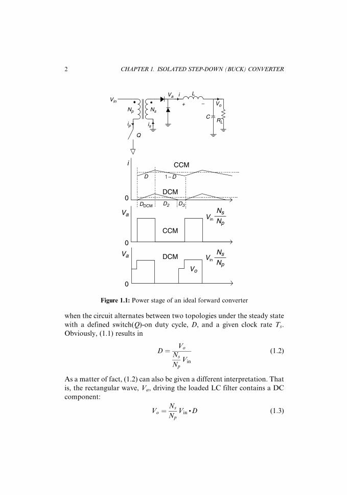
when the circuit alternates between two topologies under the steady state
with a defined switch(Q)-on duty cycle, D, and a given clock rate Ts.
Obviously, (1.1) results in
D ¼ Vo
Ns
Np
Vin
(1:2)
As a matter of fact, (1.2) can also be given a different interpretation. That
is, the rectangular wave, Va, driving the loaded LC filter contains a DC
component:
Vo ¼Ns
Np
Vin.D (1:3)
Va
VoNp Ns
Vin
L
+ −
is
i
ip
CRL
Q
Va
CCM
0
Vin
Vin
Np
Ns
Np
NsVa DCM
0
Vo
i CCM
DCM0
D
DDCM D3D2
1 − D
Figure 1.1: Power stage of an ideal forward converter
2 CHAPTER 1. ISOLATED STEP-DOWN (BUCK) CONVERTER

This latter view aligns well with the ultimate goal of the converter
operation, extracting the average voltage embedded in the transformed
input drive and regulating the output voltage by fine-tuning the turn
ratio with variable duty cycle, D.
However, in reaching (1.1)–(1.3), we made an expedient, but unreal-
istic, assumption, which is the zero forward voltage a rectifier diode
offers when it is conducting. We shall make the necessary corrections
by first forgoing the assumption of the ideal diode. Rather, the rectifier’s
forward voltage is given a nonzero value, VD. With it, and referring to
Figure 1.2, (1.1)–(1.3) are modified and become
Ns
Np
Vin � VD � Vo
� �D . Ts þ (�VD � Vo)(1�D)Ts ¼ 0 (1:4)
D ¼ Vo þ VD
Ns
Np
Vin
(1:5)
Va
Vo
Np Ns
VinL
is
i
ipRL
Rw
Ron
VD
C
RFrL
D2
−VD
Va
0
VDNp
NsVin −
Figure 1.2: Nonideal power stage
1.1. CCM OPEN-LOOP OUTPUT AND DUTY CYCLE DETERMINATION 3
Vo ¼Ns
Np
Vin. D� VD (1:6)
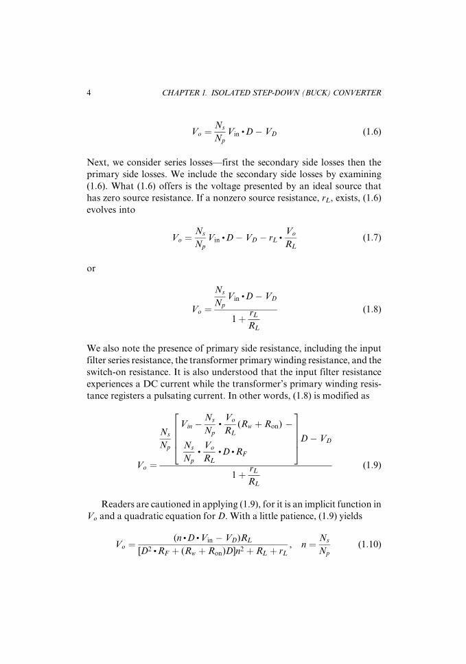
Next, we consider series losses—first the secondary side losses then the
primary side losses. We include the secondary side losses by examining
(1.6). What (1.6) offers is the voltage presented by an ideal source that
has zero source resistance. If a nonzero source resistance, rL, exists, (1.6)
evolves into
Vo ¼Ns
Np
Vin. D� VD � rL
.Vo
RL
(1:7)
or
Vo ¼
Ns
Np
Vin. D� VD
1þ rL
RL
(1:8)
We also note the presence of primary side resistance, including the input
filter series resistance, the transformer primary winding resistance, and the
switch-on resistance. It is also understood that the input filter resistance
experiences a DC current while the transformer’s primary winding resis-
tance registers a pulsating current. In other words, (1.8) is modified as
Vo ¼
Ns
Np
Vin �Ns
Np
.Vo
RL
(Rw þ Ron) �
Ns
Np
.Vo
RL
. D . RF
26664
37775D� VD
1þ rL
RL
(1:9)
Readers are cautioned in applying (1.9), for it is an implicit function in
Vo and a quadratic equation for D. With a little patience, (1.9) yields
Vo ¼(n .D . Vin � VD)RL
[D2 .RF þ (Rw þ Ron)D]n2 þ RL þ rL
, n ¼ Ns
Np
(1:10)
4 CHAPTER 1. ISOLATED STEP-DOWN (BUCK) CONVERTER

It can also be reformulated as
n2 . RF. Vo
.D2 þ [n2(Rw þ Ron)Vo � n . RL. Vin]D
þ (RL þ rL)Vo þ RL.VD ¼ 0 (1:11)
1.2 DCM Open-Loop Output and Duty CycleDetermination
The DCM operation is rarely used for actual design. However, it does
have educational merits from an analytical point of view. We consider
only diode losses for demonstration purposes. As shown in Figure 1.1,
there are three distinctive operation intervals for the DCM. It is no
longer a simple task identifying the duty cycle using the concept of
volt–second balance alone. Yes, the concept is still, and always, appli-
cable, but we need more than that. Again, we first apply Faraday’s law of
flux conservation:
n . Vin � VD � Voð ÞDDCM . Ts þ (�VD � Vo)D2 . Ts ¼ 0 (1:12)
Equation (1.12), however, has two unknowns, DDCM and D2. We need
one more equation. This need can be met by examining the inductor
current form given in Figure 1.3.
The key is the fact that the load current, Io, equals the average value
contained in the current waveform. That is,
n . Vin � VD � Vo
2 .LDDCM . Ts
. (DDCM þD2) . Ts.
1
Ts
¼ Vo
RL
(1:13)
i
DCM0
DDCM D2 D3
Io
Figure 1.3: Inductor current for DCM
1.2. DCM OPEN-LOOP OUTPUT AND DUTY CYCLE DETERMINATION 5

Equations (1.12) and (1.13) can then be solved together and the
symbolic solutions are
DDCM ¼
ffiffiffiffiffiffiffiffiffiffiffiffiffiffiffiffiffiffiffiffiffiffiffiffiffiffiffiffiffiffiffiffiffiffiffiffiffiffiffiffiffiffiffiffiffiffiffiffiffiffiffiffiffiffiffiffiffi2 . L . fs .
Vo
RL
(n . Vin � VD � Vo)n . Vin
VD þ Vo
vuuuuut (1:14)
D2 ¼
ffiffiffiffiffiffiffiffiffiffiffiffiffiffiffiffiffiffiffiffiffiffiffiffiffiffiffiffiffiffiffiffiffiffiffiffiffiffiffiffiffiffiffiffiffiffiffiffiffiffiffiffiffiffiffiffiffiffiffiffiffiffiffi(n .Vin � VD � Vo)2 . L . fs .
Vo
RL
(VD þ Vo)n . Vin
vuuut(1:15)
1.3 CCM to DCM Transition, Critical Inductance
It is very interesting tocompare (1.5) and (1.14).Theobviousdifference is in
the form of equation (1.5), which is very simple, while (1.14) looks formid-
able with all circuit components and switching frequency, fs, involved in
setting the duty cycle. Readers may then ask, What critical part does a
designer control to determine the mode of operation? The answer is the
inductor.Given the required input, output, loading, and selected switching
frequency, there is a critical inductor value that marks the boundary of
CCMtoDCMtransition.Howdoweobtain that value?There ismore than
one way to determine the critical value. We will present two approaches.
The first approach recognizes that, when the operating condition
changes to a point, the DCM duty cycle equals that of the CCM:
DDCM ¼
ffiffiffiffiffiffiffiffiffiffiffiffiffiffiffiffiffiffiffiffiffiffiffiffiffiffiffiffiffiffiffiffiffiffiffiffiffiffiffiffiffiffiffiffiffiffiffiffiffiffiffiffiffiffiffiffiffi2 .L . fs .
Vo
RL
(n . Vin � VD � Vo)n . Vin
VD þ Vo
vuuuuut ¼ Vo þ VD
n . Vin
(1:16)
Equation (1.16) yields the critical inductance:
Lcri ¼(n . Vin � VD � Vo)(Vo þ VD)
2 . fs .Vo
RL
. n . Vin
(1:17)
6 CHAPTER 1. ISOLATED STEP-DOWN (BUCK) CONVERTER

The other approach takes a little extra effort but gives additional insight.
This time, the inductor current under the CCM operation is reexamined
in Figure 1.4. An AC ripple current is superimposed on top of the DC
load current, Io.
The ripple current has a magnitude of
Di ¼ (n . Vin � VD � Vo)
LD . Ts ¼
(n . Vin � VD � Vo)(Vo þ VD)
L . fs .n . Vin
(1:18)
The trough magnitude is therefore
iA ¼Vo
RL
� (n . Vin � VD � Vo)(Vo þ VD)
2 . L . fs . n . Vin
(1:19)
It is easy to see that the power stage enters the DCM operation when the
trough current equals zero. In other words, the condition iA ¼ 0 gives the
critical inductance, and it is the same as (1.17).
1.4 Gain Formula for Nonideal OperationalAmplifiers
In most existing electronics textbooks dealing with operational ampli-
fiers, the concept of virtual ground, Figure 1.5, is often invoked. The
concept emerges from the assumption that both the noninverting, V1,
and inverting, V2, inputs track each other and that one of the inputs is
generally at a fixed DC voltage. As a result, both inputs can be treated as
zero potential for signal analysis purposes. However, both the logic
and the concept suffer unnecessarily from many deficiencies. The first,
i CCM
0
D 1 − D
iA
Io
Figure 1.4: Inductor current for CCM
1.4. GAIN FORMULA FOR NONIDEAL OPERATIONAL AMPLIFIERS 7

and perhaps the worst of all, is the assumption of infinite gain and band-
width. Second, and no worse, is the missing information about the DC
operating state. Third, the nonideal open-loop gain is not accounted for.
The situation can be improved significantly by getting rid of the
virtual ground concept and using the voltage view and the superposition
principle. Referring to Figure 1.6, the noninverting node gives Vp ¼ Vref ,
while the inverting node gives
Vn ¼Zf (s) . Vi þ Zi(s) . Vo
Zf (s)þ Zi(s)(1:20)
The output is therefore given as
+
−V1
V2
Vo
R1
R2
R3
Vin
Vref
Vo+
−V2
V1
R2
R1
R3
Vin
(a)
(b)
Figure 1.5: (a) Typical op-amp circuit, (b) inverting configuration
+
−
Vref
A(s)Zi(s)
Zf (s)
Vn
Vp
Vo
Figure 1.6: General op-amp circuit
8 CHAPTER 1. ISOLATED STEP-DOWN (BUCK) CONVERTER

Vo ¼ A(s)(Vp � Vn) ¼ A(s) Vref �Zf (s) . Vi þ Zi(s) . Vo
Zf (s)þ Zi(s)
� �(1:21)
With further manipulation, (1.21) gives
Vo ¼Vref �
Zf (s)
Zf (s)þ Zi(s). Vi
1
A(s)þ Zi(s)
Zf (s)þ Zi(s)
(1:22)
If A(s)� 0, (1.22) degenerates into
Vo ¼ 1þ Zf (s)
Zi(s)
� �Vref �
Zf (s)
Zi(s)Vi (1:23)
This is the form given in many books with the assumption of infinite
open-loop gain and bandwidth. However, we stick with (1.22) from here
on, since it accounts for the nonideal gain A(s). As a matter of fact, the
nonideal gain can also be approximated by a single, first-order pole
A(s) ¼ A0
s
2 . p . fpþ 1
(1:24)
where A0 stands for the open-loop low frequency gain of op-amp (inte-
grated circuit) and fp is the 3-db roll-off frequency. These figures are
always given in manufacturers’ data sheets.
1.5 Feedback under Voltage-Mode Control
To obtain a precise and well-regulated output voltage against input or
load changes, a feedback technique is always used in modern switch-
mode power converters. Early converters, in the 1960s, tended to use
voltage-mode control alone. By the late 1970s, the concept of current-
mode control began to show up. A typical voltage-mode control scheme
is shown in Figure 1.7.
1.5. FEEDBACK UNDER VOLTAGE-MODE CONTROL 9
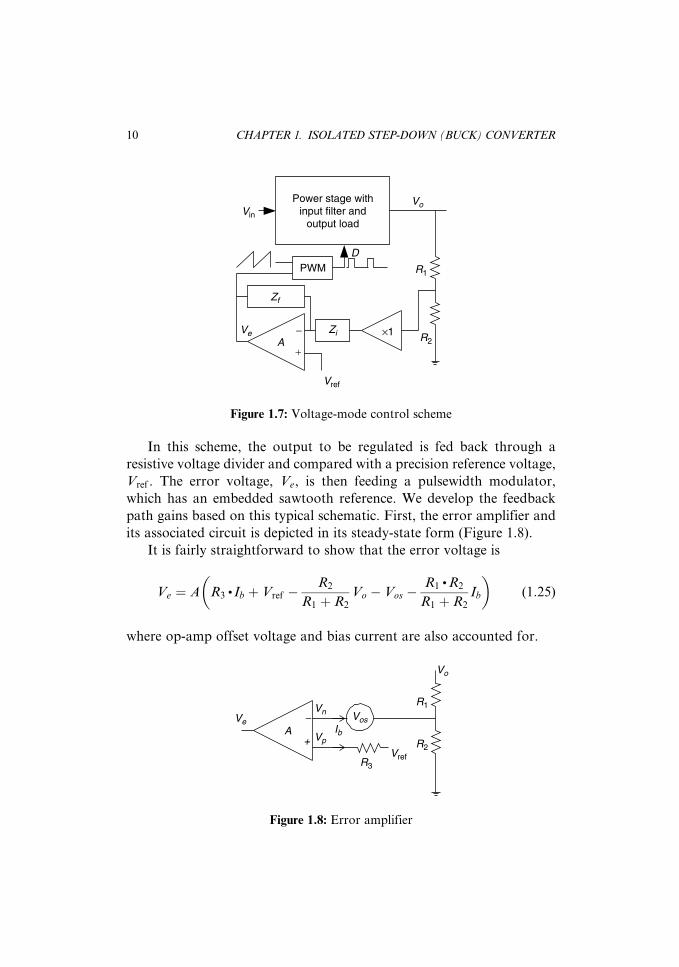
In this scheme, the output to be regulated is fed back through a
resistive voltage divider and compared with a precision reference voltage,
Vref . The error voltage, Ve, is then feeding a pulsewidth modulator,
which has an embedded sawtooth reference. We develop the feedback
path gains based on this typical schematic. First, the error amplifier and
its associated circuit is depicted in its steady-state form (Figure 1.8).
It is fairly straightforward to show that the error voltage is
Ve ¼ A R3 . Ib þ Vref �R2
R1 þ R2
Vo � Vos �R1 . R2
R1 þ R2
Ib
� �(1:25)
where op-amp offset voltage and bias current are also accounted for.
+
−
Vref
A×1
Zf
Zi
PWM
Vin
Power stage withinput filter and
output load
Vo
D
Ve
R1
R2
Figure 1.7: Voltage-mode control scheme
+
−
Vref
AVe
Vo
R1
R2Vp
Vn VosIb
R3
Figure 1.8: Error amplifier
10 CHAPTER 1. ISOLATED STEP-DOWN (BUCK) CONVERTER
Next the PWM gain is derived. In the case of voltage-mode control, it
is again quite simple. The circuit surrounding the PWM is given a little
more detail as shown in Figure 1.9.
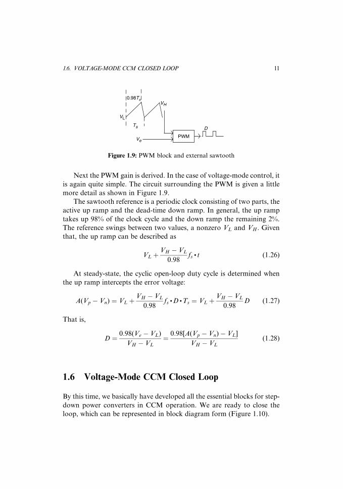
The sawtooth reference is a periodic clock consisting of two parts, the
active up ramp and the dead-time down ramp. In general, the up ramp
takes up 98% of the clock cycle and the down ramp the remaining 2%.
The reference swings between two values, a nonzero VL and VH . Given
that, the up ramp can be described as
VL þVH � VL
0:98fs . t (1:26)
At steady-state, the cyclic open-loop duty cycle is determined when
the up ramp intercepts the error voltage:
A(Vp � Vn) ¼ VL þVH � VL
0:98fs . D . Ts ¼ VL þ
VH � VL
0:98D (1:27)
That is,
D ¼ 0:98(Ve � VL)
VH � VL
¼ 0:98[A(Vp � Vn)� VL]
VH � VL
(1:28)
1.6 Voltage-Mode CCM Closed Loop
By this time, we basically have developed all the essential blocks for step-
down power converters in CCM operation. We are ready to close the
loop, which can be represented in block diagram form (Figure 1.10).
PWM
D
Ve
VH
VL
Ts
0.98Ts
Figure 1.9: PWM block and external sawtooth
1.6. VOLTAGE-MODE CCM CLOSED LOOP 11

The block diagram is intentionally partitioned (dashed line) into two
parts—the feedback path and the power stage (plant, in control system
terminology). Inside each block, the relevant equation governing the
block function is given in parentheses. Equations (1.25) and (1.28) can
be combined to give the open-loop duty cycle in terms of circuit com-
ponents and open-loop output:
D ¼0:98 A R3 . Ib þ Vref �
R2
R1 þ R2
Vo � Vos �R1 . R2
R1 þ R2
Ib
� �� VL
� �VH � VL
(1:29)
In theory, (1.29) can be further combined with (1.10) to yield the
closed-loop output. But anyone attempting to do so soon realizes that it
is a mission impossible, for (1.10) contains a D2 term and squaring (1.29)
is not a simple matter. Furthermore, even after plugging in the D2 and D
terms, (1.10) does not give the closed-loop output explicitly, because Vo
appears on both sides of the equation. One can use the approximation
(1.8) instead but at the expense of accuracy. Do we have a way out? Yes,
we can handle the situation using an implicit function. We first define
two implicit functions from (1.29) and (1.10):
p(D,Vo,Rx, ...)¼
D�0:98 A(R3 . IbþVref�
R2
R1þR2
Vo�Vos�R1 . R2
R1þR2
Ib�VL)
� �VH�VL
¼ 0 (1:30)
Feedback
Vin
PWM(1.28)
Error Amp(1.25)
Ve
Vo
DCCM
Approximation: (1.6)or (1.8)
Precise: (1.10)Power Stage
Figure 1.10: Buck converter CCM in a closed loop
12 CHAPTER 1. ISOLATED STEP-DOWN (BUCK) CONVERTER

q(D, Vo, Vin, . . .)¼Vo�(n . D . Vin�VD)RL
[D2 . RF þ (RwþRon)D]n2þRLþrL
¼0 (1:31)
Given the two functions, and using the Jacobian determinant, the output
sensitivity against all circuit components and variables can be easily
obtained. For instance, the load sensitivity is given as
@Vo
@RL
¼ �
@p
@D
@p
@RL
@q
@D
@q
@RL
��������������
@p
@D
@p
@Vo
@q
@D
@q
@Vo
��������������
(1:32)
Of course, the steady-state closed-loop output, and duty cycle can both
be solved simultaneously by solving (1.30) and (1.31) numerically using
mathematical softwareMathCAD,MATLAB,MAPLE,orMathematica.
1.7 Voltage-Mode DCM Closed Loop
As mentioned before, buck converters operating in the DCM are not
desirable. But, for academic completeness, the closed-loop formulation
for this operationmode is also given.We first consolidate (1.12) and (1.15):
Vo ¼
(n . Vin � VD)DDCM �
VD.
ffiffiffiffiffiffiffiffiffiffiffiffiffiffiffiffiffiffiffiffiffiffiffiffiffiffiffiffiffiffiffiffiffiffiffiffiffiffiffiffiffiffiffiffiffiffiffiffiffiffiffiffiffiffiffiffiffiffiffiffiffiffiffi(n .Vin � VD � Vo)2 . L . fs .
Vo
RL
(VD þ Vo)n . Vin
vuuut
266664
377775
DDCM þ
ffiffiffiffiffiffiffiffiffiffiffiffiffiffiffiffiffiffiffiffiffiffiffiffiffiffiffiffiffiffiffiffiffiffiffiffiffiffiffiffiffiffiffiffiffiffiffiffiffiffiffiffiffiffiffiffiffiffiffiffiffiffiffi(n . Vin � VD � Vo)2 . L . fs .
Vo
RL
(VD þ Vo)n . Vin
vuuut(1:33)
We then replace the power stage of Figure 1.10 with one for the DCM.
This step leads to Figure 1.11 for the DCM.
1.7. VOLTAGE-MODE DCM CLOSED LOOP 13
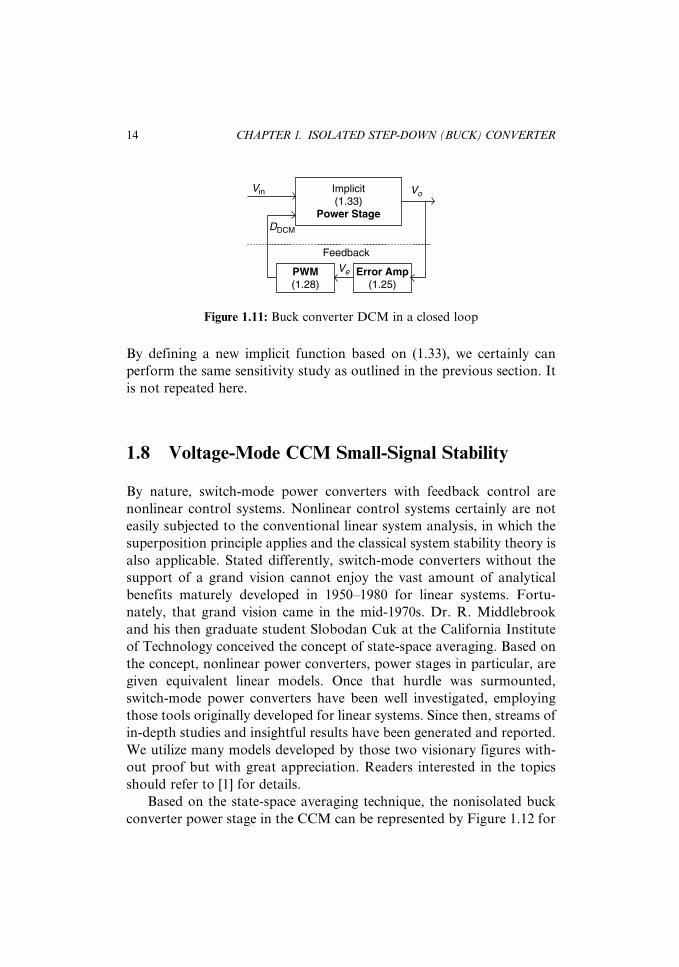
By defining a new implicit function based on (1.33), we certainly can
perform the same sensitivity study as outlined in the previous section. It
is not repeated here.
1.8 Voltage-Mode CCM Small-Signal Stability
By nature, switch-mode power converters with feedback control are
nonlinear control systems. Nonlinear control systems certainly are not
easily subjected to the conventional linear system analysis, in which the
superposition principle applies and the classical system stability theory is
also applicable. Stated differently, switch-mode converters without the
support of a grand vision cannot enjoy the vast amount of analytical
benefits maturely developed in 1950–1980 for linear systems. Fortu-
nately, that grand vision came in the mid-1970s. Dr. R. Middlebrook
and his then graduate student Slobodan Cuk at the California Institute
of Technology conceived the concept of state-space averaging. Based on
the concept, nonlinear power converters, power stages in particular, are
given equivalent linear models. Once that hurdle was surmounted,
switch-mode power converters have been well investigated, employing
those tools originally developed for linear systems. Since then, streams of
in-depth studies and insightful results have been generated and reported.
We utilize many models developed by those two visionary figures with-
out proof but with great appreciation. Readers interested in the topics
should refer to [1] for details.
Based on the state-space averaging technique, the nonisolated buck
converter power stage in the CCM can be represented by Figure 1.12 for
Feedback
Vin
PWM(1.28)
Error Amp(1.25)
Ve
Vo
DDCM
Implicit(1.33)
Power Stage
Figure 1.11: Buck converter DCM in a closed loop
14 CHAPTER 1. ISOLATED STEP-DOWN (BUCK) CONVERTER
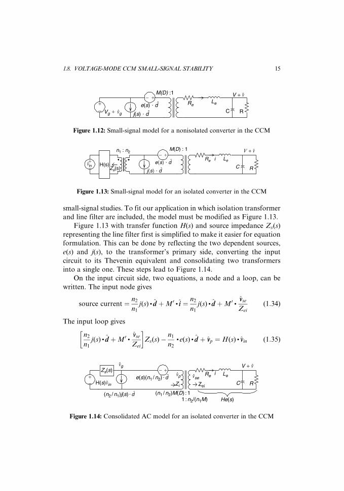
small-signal studies. To fit our application in which isolation transformer
and line filter are included, the model must be modified as Figure 1.13.
Figure 1.13 with transfer function H(s) and source impedance Zs(s)
representing the line filter first is simplified to make it easier for equation
formulation. This can be done by reflecting the two dependent sources,
e(s) and j(s), to the transformer’s primary side, converting the input
circuit to its Thevenin equivalent and consolidating two transformers
into a single one. These steps lead to Figure 1.14.
On the input circuit side, two equations, a node and a loop, can be
written. The input node gives
source current ¼ n2
n1
j(s) . dd þM0 . ii ¼ n2
n1
j(s) . dd þM0 .vvse
Zei
(1:34)
The input loop gives
n2
n1
j(s) . dd þM0 .vvse
Zei
� �Zs(s)�
n1
n2
. e(s) . dd þ vvp ¼ H(s) . vvin (1:35)
+−
−+ Re
Le
C RVg + vg j(s) ⋅ de(s) ⋅ d
V + vM(D) :1
Figure 1.12: Small-signal model for a nonisolated converter in the CCM
+−+−
Re Le
C Rj(s) ⋅ de(s) ⋅ d
V + v
vin H(s)
n1 : n2
Zs(s)
M(D) : 1
i
Figure 1.13: Small-signal model for an isolated converter in the CCM
vp
vg
vse
+−+−
Re Le
C R
(n2 / n1)j(s) ⋅ d
e(s)(n1 / n2) ⋅ d
V + v
H(s)vin
Zs(s)
(n1 / n2)M(D) : 11 : n2/(n1M)
i
ZeiZi
He(s)
Figure 1.14: Consolidated AC model for an isolated converter in the CCM
1.8. VOLTAGE-MODE CCM SMALL-SIGNAL STABILITY 15

By reflecting the secondary voltage to the primary one, (1.35) gives
n2
n1
j(s) . dd þ (M0)2 .vvp
Zei
� �Zs(s)�
n1
n2
. e(s) . dd þ vvp ¼ H(s) . vvin (1:36)
where M0 ¼ n2=(n1 . M). Equation (1.36) ultimately gives
vvp ¼
H(s) . vvin þe(s)n2
n1
1� j(s)
e(s)
n2
n1
� �2
Zs(s)
" #dd
1þ Zs(s)
n1
n2
M
� �2
Zei(s)
vvse ¼M0 . vvp
(1:37)
Equation (1.37) hints that we can translate Figure 1.14 to a block
diagram form by rewriting the equation as
vvse ¼M0[GVpg(s) . vvg þ GVpd(s) . dd] (1:38)
where
GVpg(s) ¼1
1þ Zs(s)
n1
n2
M
� �2
Zei(s)
(1:39)
and
GVpd(s) ¼
e(s)n2
n1
1� j(s)
e(s)
n2
n1
� �2
Zs(s)
" #
1þ Zs(s)
n1
n2
M
� �2
Zei(s)
(1:40)
Zei(s) ¼ Re þ Le. sþ 1
Rþ C . s
� ��1
(1:41)
16 CHAPTER 1. ISOLATED STEP-DOWN (BUCK) CONVERTER

In block diagram form, Figure 1.14 becomes Figure 1.15, where He(s) is
the effective, loaded output filter transfer function:
He(s) ¼1Rþ C . s
�1
Re þ Le. sþ 1
Rþ C . s
�1(1:42)
Again, readers are reminded that Re, Le, e(s), j(s), and several other
model parameters and variables are given in [1].
At this point, we are almost ready again to close the loop for AC
small-signal studies. However, we need three more blocks to finish the
job: the feedback ratio, the error amplifier, and the voltage-mode PWM
gain. The feedback ratio is quite simple. It is the voltage division ratio
given in Figure 1.7:
Kf ¼R2
R1 þ R2
(1:43)
The error amplifier transfer function is the inverting part of (1.23) if the
approximation is invoked. The sign is taken care of later:
EA(s) ¼ Zf (s)
Zi(s)(1:44)
If a more accurate form is desired, the error amplifier gain is the inverting
part of (1.22):
EA(s) ¼ A(s) . Zf (s)
Zf (s)þ [1þ A(s)]Zi(s)(1:45)
H(s)
Gvpg(s)
++ n2/ (n1M )Gvpd(s) He(s)
vp
vg
vse vd
vin
Figure 1.15: Small-signal block diagram for an isolated buck converter
1.8. VOLTAGE-MODE CCM SMALL-SIGNAL STABILITY 17
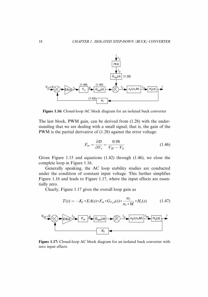
The last block, PWM gain, can be derived from (1.28) with the under-
standing that we are dealing with a small signal; that is, the gain of the
PWM is the partial derivative of (1.28) against the error voltage:
Fm ¼@D
@Ve
¼ 0:98
VH � VL
(1:46)
Given Figure 1.15 and equations (1.42) through (1.46), we close the
complete loop in Figure 1.16.
Generally speaking, the AC loop stability studies are conducted
under the condition of constant input voltage. This further simplifies
Figure 1.16 and leads to Figure 1.17, where the input effects are essen-
tially zero.
Clearly, Figure 1.17 gives the overall loop gain as
T(s) ¼ �Kf. EA(s) . Fm
.GVpd(s) .n2
n1 . M. He(s) (1:47)
H(s)
Gvpg(s)
++ n2/(n1M )Gvpd(s) He(s)
vg
vp vse vd
vin
Fm
Kf
EA(s)ve
Vref = 0+−
(1.46) (1.40)
(1.39)
(1.43)
Figure 1.16: Closed-loop AC block diagram for an isolated buck converter
++ n2/(n1M )Gvpd
(s) He(s)vsevpve vdFm
Kf
EA(s)Vref = 0
+−
Figure 1.17: Closed-loop AC block diagram for an isolated buck converter with
zero input effects
18 CHAPTER 1. ISOLATED STEP-DOWN (BUCK) CONVERTER
Furthermore, Figure 1.16 also gives the conducted susceptibility, which is
a measure of how much input perturbation ends up at the output:
Cs(s) ¼vv
vvin
¼ H(s) . GVpg(s)
n2
n1 .M. He(s)
1� T(s)(1:48)
1.9 Current-Mode Control
By nature, signals in current forms have advantages over those in voltage
form, since voltage is an accumulation of electron flux and, therefore,
slow in time as far as control mechanism is concerned. In the early 1980s,
this understanding spawned a new tide in switch-mode power supply
design, namely, the current-mode control. In this control mode, the
averaged or peak current of magnetic origin is employed in the feedback
loop of switch-mode power converters. However, by adding a current
loop, the conventional concept of loop gain is blurred, since multiple
loops exist and make it difficult to identify the main loop. The current-
mode control techniques, in addition to introducing difficulties in
loop identification, also create new territories for analysis. In this
and following sections, we give this superior technique an in-depth
study. We again cover both CCM and DCM operations using the peak
current. The average-current current-mode control is set aside and
covered in a separate chapter because of its mathematical complexity.
But, let us first look at the general feature of a current-mode control
scheme, Figure 1.18.
Evidently, the sole and key difference between Figures 1.7 and 1.18 is
the way the reference ramp is generated. In the case of voltage-mode
control, the ramp is external from the viewpoint of the power plant,
whereas for current-mode control, it is internal. However, the superficial
view alone does not unveil the superior nature of peak current-mode
control. We definitely need to probe further into the dynamics of the
technique. For that, we examine how the current sensing ramp is pro-
duced. A typical example of that is given in Figure 1.19.
1.9. CURRENT-MODE CONTROL 19

The figure shows that the instantaneous switch current is sensed by a
current transformer that provides isolation and current scaling. The
switch is turned on at a clock edge. It is turned off when the sensed
current in voltage form intercepts the error voltage, Ve (Figure 1.20).
The performance merits of current-mode control over voltage-mode
control can be appreciated more by looking at the transient response
when the converter is subjected to a step-load disturbance or a step-line
change. Figure 1.19 shows that the sensed signal has a ramp-up part.
This part is attributed to a magnetic device with a ferrous core. When
subjected to a volt–second (flux) drive, the magnetic device develops a
current. The time rate of such a current is easily expressed as
di
dt/ voltage across
inductance¼ Vinput � Vo
L(1:49)
+
−
Vref
A�1
Zf
Zi
PWM
Vin
Power stage withinput filter and
output load Vo
Currentsensing
D
R1
R2
Ve
Figure 1.18: Peak-current current-mode control scheme
PWMD
Ve
Magneticdevice
Vin
isw
CCMDCM Rs
Figure 1.19: Peak current sensing
20 CHAPTER 1. ISOLATED STEP-DOWN (BUCK) CONVERTER

The equation tells us loud and clear that the magnetic device’s current
rate of change is in phase with either the input or the output, voltage
changes that, in turn, are reflected in error voltage. In pictorial form,
Figure 1.21 shows how a step load initiates a chain of events that is the
hallmark of current-mode control.
As the figure shows, di2=dt > di1=dt when a step load commences,
given constant input. In essence, the average value of the magnetic
device’s current rapidly tracks the step load and minimizes the error
voltage. Another way of praising the mechanism is to say that the
phase delay property of a magnetic device is removed. In the jargon of
control system theory, a lagging pole is eliminated and system response
speed is improved. That is the key merit of current-mode control.
1.10 CCM Current-Mode Control in a Closed-LoopSteady State
In the previous section, the general feature of current-mode operation
and its advantages were briefly reviewed. In this section, we give a
thorough treatment of CCM. For that, we refer to Figure 1.1 (or 1.2).
The primary winding current (switch current) is understood to consist of
three components: the reflected load, the reflected ripple of the output
CCM
DCM
On Off Ve
Figure 1.20: Determination of the peak current-mode duty cycle
Iload
Vo
Ve
di1/dtdi2/dt
Figure 1.21: Current-mode control mechanism
1.10. CCM CURRENT-MODE CONTROL IN A CLOSED-LOOP STEADY STATE 21

inductor, and the primary magnetization, Lp. Given in Figure 1.22, these
will help us formulate and perform the analysis to follow.
The total ramp-up current profile can be written as
ip(t)¼Ns
Np
Io�
Ns
Np
Vin�VD�Vo
� �D
2L . fsþ
Ns
Np
Vin�VD�Vo
L. t
2664
3775þVin
Lp
. t (1:50)
Referring also to Figure 1.19 and assuming a 1-to-ni current transformer,
the steady-state open-loop duty cycle is therefore decided when the ramp-
up signal meets the error voltage; that is,
ip(D . Ts)
ni
.Rs ¼ Ve (1:51)
or
D(Ve, Vin, Vo) ¼
ni. Ve
Rs
� Ns
Np
Vo
RL
Ns
Np
Ns
Np
Vin � VD � Vo
2 . L . fsþ Vin
Lp. fs
(1:52)
Compared with (1.28) for voltage-mode control, the intricacy of cur-
rent-mode control is simply amazing. It seems to have built-in intelligence
by incorporating all the essential variables. Moreover, we can easily
modify Figure 1.10 and infuse it with the sophistication of current-mode
control. This leads to Figure 1.23, in which only the mechanism of the
PWM is modified.
For those of you interested in the closed-loop output, we do the
following procedure. But, considering that (1.10) is too prohibitively
Np
Ns Io)(Primary windingReflected output
inductance
DTs
Figure 1.22: Main switch current composition
22 CHAPTER 1. ISOLATED STEP-DOWN (BUCK) CONVERTER

complicated to use, we invoke only (1.6), the approximation. Starting
from (1.6), we replace the variable D with (1.52):
Vo ¼Ns
Np
Vin.
ni. Ve
Rs
� Ns
Np
Vo
RL
Ns
Np
Ns
Np
Vin � VD � Vo
2 . L . fsþ Vin
Lp. fs
� VD (1:53)
We then close the loop by plugging in (1.25), replacing Ve:
Vo ¼
Ns
Np
Vin
ni. A
R3 . Ib þ Vref�R2
R1 þ R2
Vo � Vos �R1 . R2
R1 þ R2
Ib
0@
1A
Rs
�Ns
Np
Vo
RL
26666666664
37777777775
Ns
Np
Ns
Np
Vin � VD � Vo
� �2 . L . fs
þ Vin
Lp. fs
� VD (1:54)
Unfortunately, even by using only the approximation, the output
voltage is still not in an explicit form. Although it is not impossible to
solve Vo symbolically, given modern software, we shall not attempt to do
so, since we would not gain more than what we have so far.
Feedback
Vin
PWM(1.52)
ErrorAmp(1.25)
Ve
Vo
DCCM
Approximation: (1.6)or (1.8)
Precise: (1.10)Power Stage
Figure 1.23: Current-mode buck converter in a CCM closed loop
1.10. CCM CURRENT-MODE CONTROL IN A CLOSED-LOOP STEADY STATE 23

1.11 CCM Current-Mode Control Small-SignalStability
In the previous section, it was mentioned that the sole difference between
Figures 1.10 and 1.23 is the PWM block. This statement holds true for
AC small-signal studies. We then modify whatever surrounds the PWM,
Fm, in Figure 1.16. This is done by expressing the total derivative of
(1.52) in terms of three partial derivatives against error voltage pertur-
bation, input disturbance, and output deviation:
dD ¼ @D
@Ve
dVe þ@D
@Vin
dVin þ@D
@Vo
dVo
¼ Fm. dVe þ Fvb
. dVin þ Fv. dVo (1:55)
where, for instance,
Fm ¼@D(Ve, Vin, Vo)
@Ve
¼ 1
Ns
Np
Ns
Np
Vin � VD � Vo
2 . L . fsþ Vin
Lp. fs
.ni
Rs
(1:56)
The other two gain coefficients, Fvb( ¼ @D=@Vin) and Fv( ¼ @D=@Vo),
in symbolic forms are extremely burdensome to write and omitted in
print with the understanding that they are readily computable given
modern software. Anyway, (1.55) needs a new block description, Figure
1.24, for a current-mode PWM.
Then, using Figure 1.24, we replace the Fm block in Figure 1.16. The
complete block diagram, Figure 1.25, for CCM operation is done. It
++
+
Fvb
Fm
Fv
dD
dVin
dVe
dVo
Figure 1.24: A current-mode CCM PWM
24 CHAPTER 1. ISOLATED STEP-DOWN (BUCK) CONVERTER

clearly reflects the added complexity of the current-mode control mech-
anism.
Again, for loop gain evaluation, Figure 1.25 is simplified by assuming
constant input. This simplification leads to Figure 1.26.
Figure 1.26 shows two loops, an inner current loop and an outer
voltage loop. We first absorb the current loop, and Figure 1.26 is further
simplified to Figure 1.27.
The loop gain for current-mode control is, by inspection,
T(s) ¼ �Kf. EA(s) . Fm
.
Gvpd(s) .n2
n1 . M(D).He(s)
1� Fv. Gvpd(s) .
n2
n1 . M(D). He(s)
(1:57)
Figure 1.25 also gives the current-mode CCM conducted susceptibility
H(s)
Gvpg(s)
Gvpd (s) +
+ n2/(n1M ) He(s)vsevpve
v
vin
vg
EA(s)Vref = 0
+−+++
Fm
Fvb
Fv
Kf
dD(1.56) (1.40)
(1.39)
(1.43)
Figure 1.25: Closed-loop AC block diagram for the CCM current mode
n2/(n1M)Gvpd(s) He(s)vsevpve v
EA(s)Vref = 0
+−++
+Fm
Fv
Kf
dD
Figure 1.26: CCM current-mode closed-loop diagram for loop gain
1.11. CCM CURRENT-MODE CONTROL SMALL-SIGNAL STABILITY 25

Cs(s) ¼ H(s) .
Gvpg(s) . M0 .He(s) þFvb
. Gvpd(s) . M0 . He(s)
1� [Fv þ Kf. EA(s) . Fm]Gvpd(s) . M0 .He(s)
8><>:
9>=>; (1:58)
1.12 Output Capacitor Size and AcceleratedSteady-State Analysis
The output filter capacitor,C in Figure 1.1, plays a major role in setting the
output ripple voltage amplitude, which always is considered a very im-
portant part of power supply specification. As such, a reliable technique
for selecting the appropriate capacitor value tied to a given ripple require-
ment is highly sought after. We study two techniques for the CCM: one
graphic based and one time-domain based. In the first approach, we
reexamine the output inductor current in detail (Figure 1.28).
It is understood that the capacitor passes only AC current. Therefore,
the triangular area above Io and its equivalent charge, dQ, can be placed
in an equation connecting the ripple requirement dv and the capacitor
value required:
v
Kf
EA(s)ve
Vref = 0+− Fm
1 − Fv
n1 × M(D)
n2
n1 × M(D)
n2
Gvpd (s)
Gvpd(s)
× He(s)
• He(s)
×
• •
Figure 1.27: CCM closed-loop diagram with the current loop absorbed
i
0DTs (1 − D)Ts
Io
Ts /2
δi
Figure 1.28: CCM output inductor current
26 CHAPTER 1. ISOLATED STEP-DOWN (BUCK) CONVERTER

C ¼ dQ
dv¼
1
2.
di
2.T
2dv
¼ di
8 . dv . fs¼
Vo þ VD
L(1�D)Ts
8 . dv . fs
¼
(Vo þ VD) 1� Vo þ VD
Ns
Np
Vin
0BB@
1CCA
8 . L . dv . f 2s
(1:59)
This first approach, however, has some deficiencies. We all under-
stand that an LC filter without damping exhibits peaking that can easily
destabilize a converter loop. Although the load resistance also provides
damping, load-dependent damping is not desirable. A well-designed
output filter generally incorporates critical damping that comes in the
form of Figure 1.29.
With damping included, (1.59) is no longer applicable because of
unknown current division between two capacitor branches. Wu [2] pre-
sented an interesting way of choosing values for both capacitors. It was
based on the equation form and the requirement of critical damping.
Readers are encouraged to refer to the book. Here, we offer another way,
based on the time-domain analysis and the concept of continuity of state.
The driving source is identified as vg with two alternating states and a duty
cycle D at switching frequency fs. The input loop gives a voltage equation:
di
dtþ rL
L. i þ 1
L. v ¼ vg
L(1:60)
The damping capacitor node gives a current equation:
dvd
dtþ 1
rd. Cd
. vd �1
rd. Cd
. v ¼ 0 (1:61)
vL
C RL
rd
Cd
rL
−VD
Np
NsVin −VD
i
vd
Figure 1.29: Output filter with damping
1.12. OUTPUT CAPACITOR SIZE AND ACCELERATED STEADY-STATE 27

The output node yields another current equation:
� 1
C. i � 1
rd. C
. vd þdv
dtþ 1
rd
þ 1
RL
� �1
C. v ¼ 0 (1:62)
By taking a Laplace transformation with unknown starting condi-
tions, I0, Vd0, and V0, (1.60)–(1.62) are transformed to
sþ rL
L
� �I(s)þ 1
L.V (s) ¼ I0 þ
Vg(s)
L(1:63)
sþ 1
rd.Cd
� �Vd(s)�
1
rd. Cd
. V (s) ¼ Vd0 (1:64)
� 1
C. I(s)� 1
rd. C
.Vd(s)þ sþ 1
rd
þ 1
RL
� �1
C
� �V (s) ¼ V0 (1:65)
The transformed equation set gives
I(s) ¼
I0 þVg(s)
L0
1
L
Vd0 sþ 1
rd. Cd
� �� 1
rd. Cd
V0 � 1
rd. C
sþ 1
rd
þ 1
RL
� �1C
� �
�������������
�������������De(s)
(1:66)
Vd (s) ¼
sþ rL
L
� �I0 þ
Vg(s)
L
1
L
0 Vd0 � 1
rd. Cd
� 1
CV0 sþ 1
rd
þ 1
RL
� �1
C
� �
�������������
�������������De(s)
(1:67)
V (s) ¼
sþ rL
L
� �0 I0 þ
Vg(s)
L
0 sþ 1
rd. Cd
� �Vd0
� 1
C� 1
rd. C
V0
������������
������������De(s)
(1:68)
28 CHAPTER 1. ISOLATED STEP-DOWN (BUCK) CONVERTER

where
De(s) ¼
sþ rL
L
� �0
1
L
0 sþ 1
rd. Cd
� �� 1
rd. Cd
� 1
C� 1
rd. C
sþ 1
rd
þ 1
RL
� �1
C
� �
������������
������������(1:69)
The numerator of the inductor current transfer function can be
expanded and grouped. The transfer function is then expressed as
I(s) ¼
sþ 1
rd. Cd
� �� 1
rd. Cd
� 1
rd. C
sþ 1
rd
þ 1
RL
� �1
C
� ���������
��������De(s)
I0
þ
�0
1
L
� 1
rd. C
sþ 1
rd
þ 1
RL
� �1
C
� ���������
��������De(s)
Vd0
þ
01
L
sþ 1
rd.Cd
� �� 1
rd. Cd
��������
��������De(s)
V0
þ
sþ 1
rd. Cd
� �� 1
rd. Cd
� 1
rd. C
sþ 1
rd
þ 1
RL
� �1
C
� ���������
��������L . De(s)
Vg(s) (1:70)
With a little patience, we can do the same thing for Vd(s) and V(s).
We also understand that the corresponding Vg(s) is
Vg(s) ¼
Ns
Np
Vin � VD
� �1
s¼ Vga(s) 0 < t < D .Ts
�VD
s¼ Vgb(s) D . Ts < t < Ts
8>><>>: (1:71)
1.12. OUTPUT CAPACITOR SIZE AND ACCELERATED STEADY-STATE 29

if we designate the time interval 0 < t < D . Ts as a and D . Ts < t < Ts as
b. Then, during the a interval, the inductor current transfer function
(1.70) can be placed in (1.72) with unknown starting states designated
as I0a, Vd0a, and V0a:
Ia(s) ¼ F1(s) . I0a þ F2(s) . Vd0a þ F3(s) . V0a
þ
sþ 1
rd. Cd
� �� 1
rd. Cd
� 1
rd.C
sþ 1
rd
þ 1
RL
� �1
C
� ���������
��������L . De(s)
Vga(s)
¼ F1(s) . I0a þ F2(s) . Vd0a þ F3(s) . V0a þ F4(s) (1:72)
We can do the same for the damping capacitor voltage and the output
voltage:
Vda(s) ¼ G1(s) . I0a þ G2(s) .Vd0a þ G3(s) . V0a þ G4(s) (1:73)
Va(s) ¼ H1(s) . I0a þH2(s) . Vd0a þH3(s) . V0a þH4(s) (1:74)
By the same token, during interval b with unknown starting states
designated as I0b, Vd0b, and V0b and considering time shift (delay) and
driving source change, the three transfer functions become
Ib(s) ¼
F1(s) . I0b þ F2(s) .Vd0b þ F3(s) . V0bþ
sþ 1
rd. Cd
� �� 1
rd. Cd
� 1
rd. C
sþ 1
rd
þ 1
RL
� �1
C
� ���������
��������L . De(s)
Vgb(s)
8>>>>>>>><>>>>>>>>:
9>>>>>>>>=>>>>>>>>;
e�D . Ts. s
¼ [F1(s) . I0b þ F2(s) . Vd0b þ F3(s) . V0b þ F5(s)]e�D . Ts
. s (1:75)
Vdb(s)¼ [G1(s) . I0bþG2(s) .Vd0bþG3(s) .V0bþG5(s)]e�D . Ts
. s (1:76)
Vb(s)¼ [H1(s) . I0bþH2(s) . Vd0bþH3(s) .V0bþH5(s)]e�D . Ts
. s (1:77)
30 CHAPTER 1. ISOLATED STEP-DOWN (BUCK) CONVERTER

Next we perform inverse Laplace transformation of (1.72)–(1.74) and
obtain
ia(t) ¼ f1(t) . I0a þ f2(t) .Vd0a þ f3(t) .V0a þ f4(t) (1:78)
vda(t) ¼ g1(t) . I0a þ g2(t) . Vd0a þ g3(t) . V0a þ g4(t) (1:79)
va(s) ¼ h1(t) . I0a þ h2(t) . Vd0a þ h3(t) . V0a þ h4(h) (1:80)
Equations (1.78)–(1.80) certainly can be placed in a matrix form:
ia(t)
vda(t)
va(t)
24
35 ¼ f1(t) f2(t) f3(t)
g1(t) g2(t) g3(t)
h1(t) h2(t) h3(t)
24
35 I0a
Vd0a
V0a
24
35þ f4(t)
g4(t)
h4(t)
24
35 (1:81)
Then, at t ¼ D . Ts, (1.81) results in
ia(D .Ts)
vda(D . Ts)
va(D . Ts)
24
35 ¼ f1(D . Ts) f2(D . Ts) f3(D . Ts)
g1(D .Ts) g2(D .Ts) g3(D .Ts)
h1(D .Ts) h2(D .Ts) h3(D .Ts)
24
35 I0a
Vd0a
V0a
24
35
þf4(D . Ts)
g4(D . Ts)
h4(D . Ts)
24
35 (1:82)
We place (1.82) in compact, closed form:
A1 . Xa þ B1 ¼ Xb (1:83)
where
A1 ¼f1(D . Ts) f2(D . Ts) f3(D . Ts)
g1(D . Ts) g2(D . Ts) g3(D . Ts)
h1(D . Ts) h2(D . Ts) h3(D . Ts)
264
375,
B1 ¼f4(D . Ts)
g4(D . Ts)
h4(D . Ts)
264
375, Xa ¼
I0a
Vd0a
V0a
264
375, Xb ¼
I0b
Vd0b
V0b
264
375 (1:84)
1.12. OUTPUT CAPACITOR SIZE AND ACCELERATED STEADY-STATE 31
What (1.83) means is that the yet unknown starting states, Xa, propa-
gates to the end states, Xb, during interval a. We repeat a similar
procedure for (1.75)–(1.77) using Xb as the starting state for interval b:
ib(t) ¼ f1(t�D . Ts) . I0b þ f2(t�D . Ts) .Vd0b
þ f3(t�D .Ts) . V0b þ f5(t�D . Ts) (1:85)
vdb(t) ¼ g1(t�D . Ts) . I0b þ g2(t�D . Ts) . Vd0b
þ g3(t�D . Ts) .V0b þ g5(t�D . Ts) (1:86)
vb(t) ¼ h1(t�D .Ts) . I0b þ h2(t�D . Ts) .Vd0b
þ h3(t�D . Ts) . V0b þ h5(t�D . Ts) (1:87)
Equations (1.85)–(1.87) can be placed in matrix form, too:
ib(t)
vdb(t)
vb(t)
264
375 ¼
f1(t�D . Ts) f2(t�D . Ts) f3(t�D . Ts)
g1(t�D . Ts) g2(t�D . Ts) g3(t�D . Ts)
h1(t�D . Ts) h2(t�D . Ts) h3(t�D . Ts)
264
375
I0b
Vd0b
V0b
264
375
þf5(t�D . Ts)
g5(t�D .Ts)
h5(t�D .Ts)
264
375 (1:88)
Then, at t ¼ Ts and considering that the end states of interval b must
equal the starting states of interval a under a steady state, the following is
derived from (1.88) (if the wraparound is not met, it is not a steady state):
f1[(1�D)Ts] f2[(1�D)Ts] f3[(1�D)Ts]
g1[(1�D)Ts] g2[(1�D)Ts] g3[(1�D)Ts]
h1[(1�D)Ts] h2[(1�D)Ts] h3[(1�D)Ts]
264
375
I0b
Vd0b
V0b
264
375
þf5[(1�D)Ts]
g5[(1�D)Ts]
h5[(1�D)Ts]
264
375 ¼
I0a
Vd0a
V0a
264
375 (1:89)
In matrix form, (1.89) gives
A2 .Xb þ B2 ¼ Xa (1:90)
32 CHAPTER 1. ISOLATED STEP-DOWN (BUCK) CONVERTER

where matrices A2 and B2 are self-evident.
Equations (1.83) and (1.90) together give
Xa ¼ (I � A2 . A1)�1(A2 . B1 þ B2) (1:91)
In other words, under a steady state, the unknown starting state
vector actually is not unknown at all. Given Xa, Xb (1.83) follows. And
the complete, cyclic steady-state solution of the circuit is done. For
instance, the inductor current is
i(t) ¼ f1(t) f2(t) f3(t)½ �Xa þ f4(t)f g u(t)� u(t�D . Ts)½ �
þ[ f1(t�D . Ts) f2(t�D . Ts) f3(t�D . Ts)]Xb
þ f5(t�D . Ts)
� �
. [u(t�D .Ts)� u(t� Ts)] (1:92)
As for the damping capacitor and the output voltages, they have
similar forms, of course, and are not repeated here. Anyway, given
vd(t) and v(t), the damping resistor power can also be described analyt-
ically:
pr(t) ¼[v(t)� vd(t)]
2
r(1:93)
This is to say the preceding technique can easily identify a filter
capacitor’s esr power dissipation and RMS current, if so desired. This
latter benefit is not readily obtainable by other means.
1.13 A Complete Example
A. Closed-Loop Output Equation
Refer to Figure 1.30, showing the schematic of a forward converter with
peak current-mode control. The operation of the converter can be briefly
described as follows. At the initiation of an internal clock, fs, residing in
the PWM integrated circuit, SG1843 (silicon general semiconductor), the
1.13. A COMPLETE EXAMPLE 33
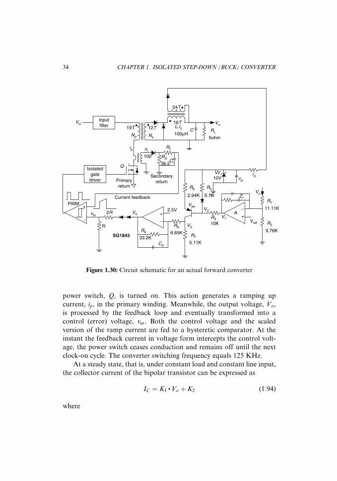
power switch, Q, is turned on. This action generates a ramping up
current, ip, in the primary winding. Meanwhile, the output voltage, Vo,
is processed by the feedback loop and eventually transformed into a
control (error) voltage, ver. Both the control voltage and the scaled
version of the ramp current are fed to a hysteretic comparator. At the
instant the feedback current in voltage form intercepts the control volt-
age, the power switch ceases conduction and remains off until the next
clock-on cycle. The converter switching frequency equals 125 KHz.
At a steady state, that is, under constant load and constant line input,
the collector current of the bipolar transistor can be expressed as
IC ¼ K1 . Vo þ K2 (1:94)
where
+
−+
−
+
−
R1
R2
11.11K
9.76K
R3
R5R6
10K
5.11K2.94K
R7
5.11K
R8
6.65KR9
33.2K
R
2RV1
V2
V3
V4
Vref
2.5V
rpcp
Vz10V
Vo
PWM
SG1843
24T
16T19T 12T
Vo
RL
5ohm
RS
36.5
Current feedback
Isolatedgatedriver
Inputfilter
Vin
ni
100
Primaryreturn
Secondaryreturn
Q
Np Ns
L,rL
100µH
ip
Vbe
ver A
Zf
Rf
Cf
Cd
C
Figure 1.30: Circuit schematic for an actual forward converter
34 CHAPTER 1. ISOLATED STEP-DOWN (BUCK) CONVERTER
K1 ¼A . R5 .
R2
R1 þ R2
. hFE
R5 .R3 þ (1þ hFE)R6 . (R3 þ R5)(1:95)
K2 ¼�A .R5 . Vref þ R3 . VD þ R5 . Vz � (R3 þ R5)Vbe
R5 . R3 þ (1þ hFE)R6 . (R3 þ R5). hFE (1:96)
Succeeding control voltage ver, equivalent to Ve of Figure 1.18, can also
be expressed as
ver ¼ K3 . Vo þ K4 (1:97)
where
K3 ¼ �2
3.
R7 . R9
R7 þ R8
.K1
K4 ¼2
32:5 1þ R9
R8
� �� R7 .R9
R7 þ R8
.K2 �2:5R7 . R9
(R7 þ R8)R8
� 2VD
� �(1:98)
and VD stands for either signal diode forward drop or rectifier diode
forward voltage.
Equations (1.50)–(1.52) give the open-loop, steady-state duty cycle,
while (1.53) gives the open-loop output. For closed-loop output, we
replace the control error voltage Ve in (1.53) with (1.97):
Vo ¼Ns
Np
Vin.
ni(K3 . Vo þ K4)
RS
�NS
Np
Vo
RL
NS
Np
NS
Np
Vin � VD � Vo
2 . L . fSþ Vin
Lp. fS
� VD (1:99)
In theory, one can plug in K4, K3, K2, and K1 in succession and
express the closed-loop output as an implicit function. But such an
expression is so unruly we have to leave it as it is and use numerical
computation instead. However, it is not a total waste, because we can use
the Jacobian technique outlined in (1.30)–(1.32) to perform very mean-
ingful studies.
1.13. A COMPLETE EXAMPLE 35

B. Closed-Loop AC Studies
For AC small-signal (designated in lower case letters) loop gain studies,
we need more preparation. We begin with the error amplifier. Figure 1.31
gives the corresponding small-signal equivalent circuit of the error am-
plifier. Based on the equivalent circuit and by also considering the non-
ideal gain, A(s), of the operational amplifier, the input-to-output transfer
function is obtained.
v1
vo
¼ �Kf. EA(s), EA(s) ¼ A(s)
Rp
1
Rp
þ 1þ A(s)
Zf (s)
� � , Kf ¼R2
R1 þ R2
(1:100)
where Rp ¼ R1==R2 and
A(s) ¼ A
s
2 . p . fpþ 1
� � (1:101)
represents the open-loop gain of the operational amplifier with single-
pole gain-rolloff at frequency fp and DC gain A.
For the transistor voltage-to-current converter, more steps are in-
volved. Figure 1.32 gives both the DC and AC circuits. Three nodal
equations at v1, v2, and v3 can be written for Figure 1.32(b).
+
−R1
R2
V1Vref
Vo
A
Zf
+
−
V1A
Zf
R1/R2
Kf × Vo
Figure 1.31: Error amplifier
36 CHAPTER 1. ISOLATED STEP-DOWN (BUCK) CONVERTER

1
R3
þ 1
R5
þ 1
hie
� �v1 �
1
hie
v2 ¼vs2
R5
þ vs1
R3
,
1þ hfe
hie
v1 �1
R6
þ 1þ hfe
hie
� �v2 ¼ �
vs2
R6
,
hfe
hie
v1 �hfe
hie
v2 þ1
Rcp
v3 ¼ 0, Rcp ¼R7R8
R7 þ R8
(1:102)
The equation set yields, at node v3,
v3 ¼
1
R3
þ 1
R5
þ 1
hie
�1
hie
vs2
R5
þ vs1
R3
1þ hfe
hie
� 1
R6
þ 1þ hfe
hie
� ��vs2
R6
hfe
hie
�hfe
hie
0
���������������
���������������De
(1:103)
and the transistor stage gains
R3
R5R6
hie
hfeib
ib
v1v2
Vs1
Vs2
(1 + hfe)ib
R8
R3
R8R7
v3
R5R6
R7
V3
V2
Vbe
(b)(a)
Figure 1.32: Transistor voltage-to-current converter: (a) DC, (b) AC
1.13. A COMPLETE EXAMPLE 37

Gt1(s) ¼@v3
@vs2
¼
1þ hfe
hie
� 1
R6
þ 1þ hfe
hie
� �hfe
hie
� hfe
hie
���������
���������1
R5
þ
1
R3
þ 1
R5
þ 1
hie
�1
hie
hfe
hie
� hfe
hie
��������
��������1
R6
De
(1:104)
Gt2(s) ¼@v3
@vs1
¼
1þ hfe
hie
� 1
R6
þ 1þ hfe
hie
� �hfe
hie
� hfe
hie
���������
���������1
R3
De
where
De ¼
1
R3
þ 1
R5
þ 1
hi
�1
hi
0
1þ hf
hi
� 1
R6
þ 1þ hf
hi
� �0
hf
hi
�hf
hi
1
Rcp
�������������
�������������(1:105)
Following the voltage-to-current converter, the internal error amplifier
of the PWM IC yields one more transfer function, based on Figure 1.33:
Gs(s) ¼ver
v3
¼ � 1
3.
1
R9
þ Cd. s
� ��1
R8
(1:106)
+
−R8R9
1/3
Cd
+
−
R9
R
2R V4
SG1843
Cd
R8
2.5V
(a) (b)
Figure 1.33: PWM internal error amplifier: (a) DC, (b) AC
38 CHAPTER 1. ISOLATED STEP-DOWN (BUCK) CONVERTER

The local supply supporting the voltage-to-current converter also pre-
sents a sneaky transfer function (Figure 1.34):
Gc(s) ¼ �24
16.
1
rz
þ cp. s
� ��1
rp þ1
rz
þ cp. s
� ��1(1:107)
With both the effective error voltage and the current feedback available
at the input terminals of the PWM comparator, the steady-state duty
cycle is established, given by (1.52). Based on (1.52), PWM gain factors
are given by (1.55) and (1.56) and so forth. The next block to be treated is
the output filter, including the main load and any housekeeping load.
This block is shown in Figure 1.35, in which Zh represents the internal
housekeeping circuit, ZL the main load, and other parasitic elements.
Its transfer function, transformer secondary to output, is
He(s) ¼ZhZL
(Zh þ Zm)1
Zh
þ 1
Zm
� ��1
þrw
" # (1:108)
In section 1.8, a state-space averaged model is invoked to derive (1.34)–
(1.40) for power stage transfer functions. A slightly simpler and just as
effective approach can also be taken for power stage. We use (1.8) and do
the following:
dVo ¼n . Vin
1þ rL
RL
. dDþ n . D
1þ rL
RL
. dVin ¼ Gpd. dDþ Gpv
. dVin (1:109)
rp
cpVz
12V
24T
16T
To v-i convertertransistor
10VVo
rz
Figure 1.34: Housekeeping supply
1.13. A COMPLETE EXAMPLE 39

The form of (1.109) suggests a summation similar to Figure 1.24 for
PWM gains. This concludes the development of individual transfer func-
tions for all key blocks. They can all be interconnected in the overall
block diagram of Figure 1.36.
For loop gain studies, Figure 1.36 can be further simplified to Figure
1.37, since the input voltage, in general, is held constant for the purpose.
Two more steps will absorb the two inner loops, one due to current
mode control and the other due to the transconductance amplifier. Once
that is done, the loop gain is easily given as
Zh
ZL
Zm
rw
Zi
Inputfilter Zs
iL
Figure 1.35: Output filter and source impedance interactions
+−
+
++
++
vref
Input filter
EA(s)
Gt1
Gt2 Gs(s)
Gc(s)
He(s)
Kf
Fm
Fv
Gpd
Gpv
+
++
Fvb Zs
Zeiver vo
dD
Figure 1.36: Overall block diagram
40 CHAPTER 1. ISOLATED STEP-DOWN (BUCK) CONVERTER

T(s) ¼Kf
. EA(s) . Gt2(s) . Gs(s) . Fm.
Gpd. He(s)
1� Fv .Gpd. He(s)
1� Gt1(s) .Gc(s) . Gs(s) . Fm.
Gpd.He(s)
1� Fv. Gpd
. He(s)
.
1� Zs(s)
Rei
1þ Zs(s)
Zei(s)
(1:110)
Readers can refer to [1] for the last impedance interaction factor in
(1.110). Anyway, for the example given, (1.110) gives the theoretical
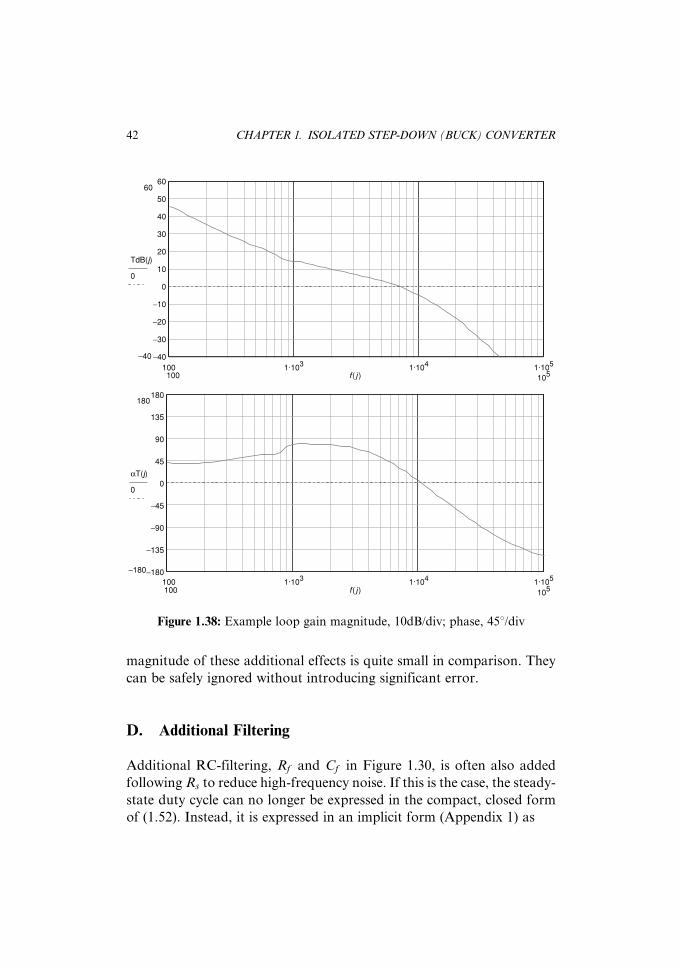
loop gain shown in Figure 1.38. The theoretical prediction compares
very well against the actual measurement (Figure 1.39).
C. Power Stage Losses
In the process leading to (1.8), the series resistive losses of the power
stage were not included. If more accuracy is required, (1.9) should be
used. With (1.9), the power stage gains are modified:
Gpdm ¼@Vo(D,Vin)
@D, Gpvm ¼
@Vo(D, Vin)
@Vin
(1:111)
In (1.9), Rw stands for the series winding resistance of input filter
inductor, Ron the MOSFET on-resistance. It is also understood that the
primary winding resistance and the MOSFET on-resistance experience
the pulsating reflected load current, while the series winding resistance of
the input filter sees only the averaged reflected load. However, the
+−
+
++
++
vref EA(s)
Gt1
Gt2 Gs(s)
Gc (s)
He(s)
Kf
Fm
Fv
Gpdver vo
d D
Figure 1.37: Simplified block diagram
1.13. A COMPLETE EXAMPLE 41
magnitude of these additional effects is quite small in comparison. They
can be safely ignored without introducing significant error.
D. Additional Filtering
Additional RC-filtering, Rf and Cf in Figure 1.30, is often also added
following Rs to reduce high-frequency noise. If this is the case, the steady-
state duty cycle can no longer be expressed in the compact, closed form
of (1.52). Instead, it is expressed in an implicit form (Appendix 1) as
100100
1.103 1.104 1.105
100100
1.103 1.104 1.105
105
105
−40
−30
−20
−10
−40
6060
50
40
30
20
10
0
TdB(j)
0
180
−180−180
135
−135
90
−90
45
−45
0
180
αT(j)
0
f ( j )
f ( j )
Figure 1.38: Example loop gain magnitude, 10dB/div; phase, 458/div
42 CHAPTER 1. ISOLATED STEP-DOWN (BUCK) CONVERTER
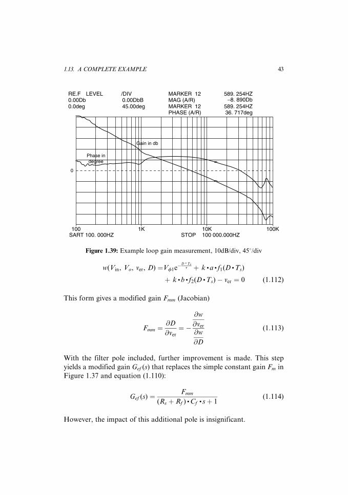
w(Vin, Vo, ver, D) ¼Vf1e�D . Ts
t þ k . a . f1(D . Ts)
þ k . b . f2(D . Ts)� ver ¼ 0 (1:112)
This form gives a modified gain Fmm (Jacobian)
Fmm ¼@D
@ver
¼ �
@w
@ver
@w
@D
(1:113)
With the filter pole included, further improvement is made. This step
yields a modified gain Gef (s) that replaces the simple constant gain Fm in
Figure 1.37 and equation (1.110):
Gef (s) ¼Fmm
(Rs þ Rf ) . Cf. sþ 1
(1:114)
However, the impact of this additional pole is insignificant.
Gain in db
Phase indegree
0
RE.F0.00Db 0.00DbB
45.00deg0.0deg
LEVEL /DIV MARKER 12
MARKER 12PHASE (A/R)
MAG (A/R) −8. 890Db589. 254HZ36. 717deg
589. 254HZ
100SART 100. 000HZ STOP 100 000.000HZ
1K 10K 100K
Figure 1.39: Example loop gain measurement, 10dB/div, 458/div
1.13. A COMPLETE EXAMPLE 43
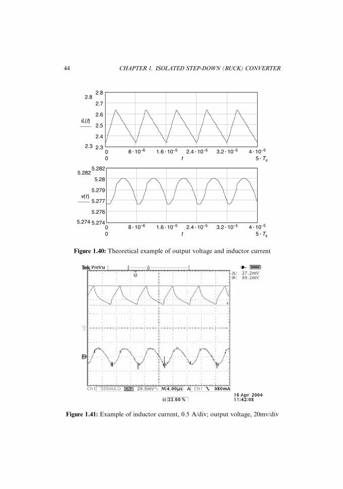
2.32.3
2.4
2.5
2.6
2.7
2.82.8
iL(t)
00
4 . 10−53.2 . 10−52.4 . 10−51.6 . 10−58 . 10−6
5 . Ts
5.2745.274
5.276
5.277
5.279
5.28
5.2825.282
v(t )
t
00
4 . 10−53.2 . 10−52.4 . 10−51.6 . 10−58 . 10−6
5 . Tst
Figure 1.40: Theoretical example of output voltage and inductor current
Figure 1.41: Example of inductor current, 0.5 A/div; output voltage, 20mv/div
44 CHAPTER 1. ISOLATED STEP-DOWN (BUCK) CONVERTER

E. Output Ripple
By applying the accelerated steady-state analysis technique outlined in
section 1.12, the output voltage ripple and output inductor current are
predicted (Figure 1.40). Theymatch the actual measurement (Figure 1.41).
1.14 State Transition Technique
In section 1.12, a technique called accelerated steady-state analysis was
invoked to obtain expeditiously the main output including ripple under
the steady state. The technique calls for many Laplace transformations
and its inverse. The approach can quickly become unmanageable if the
order of circuit exceeds three. In this section, we present a different
approach that deals with everything directly in the time domain. We
use Figure 1.29 as the basis. Since the present goal is to introduce the
technique, we use a simplified version of Figure 1.29, deleting rd and Cd
and adding rC as esr for the main filter capacitor, C. In other words, we
are dealing with Figure 1.42.
With the inductor current, i, and the capacitor voltage, v, selected as
the two state variables, the following is established:
d
dtx ¼ d
dt
i
v
� �¼� rL þ Rp
L� k
LRp
rC. C
� 1� k
rC. C
264
375 i
v
� �þ
1L
0
� �E ¼ A .xþ B . E
(1:115)
where Rp equals rc in parallel with RL, while E stands for the rectangular
input source driving the filter; A and B are the state matrix; x is the state
v
L
RL
rC
C
rL
−VD
VDN
p
NsV
in-
i vo
Figure 1.42: Simplified output filter
1.14. STATE TRANSITION TECHNIQUE 45

vector. It is well known in linear system theory, linear algebra, and
matrix theory that the solution for (1.115) can be given as
x(t) ¼ eA . t .x(0)þðt
0
eA(t�t) . B .E .dt (1:116)
Furthermore, if the driving source happens to be constant during the
time of interest, the solution is reduced to
x(t) ¼ eA . t . x(0)� A�1(I � eA . t)B . E (1:117)
Referring to Figure 1.42 and assuming two unknown starting
states—x(0) ¼ X1 for the on-time segment, DTs, and x(0) ¼ X2 for the
off-time segment, (1�D)Ts—we arrive at two solutions for the two
segments, DTs and (1�D)Ts:
x1(t) ¼ eA . t . X1 � A�1 I � eA . t
BNs
Np
Vin � VD
� �
x2(t) ¼ eA(t�D . Ts) . X2 þ A�1h1� eA(t�D . Ts)
iB . VD
(1:118)
Three items, the matrix exponential, X1, and X2, need to be evalu-
ated. We first find the starting states. For that, we apply the concept of
continuity of states at the two time boundaries, t ¼ DTs for x1(t) and
t ¼ Ts for x2(t):
eA . D . Ts .X1 � A�1 I � eA . D . T
BNs
Np
Vin � VD
� �¼ X2
eA . (1�D) . Ts .X2 þ A�1hI � eA . (1�D) . T
iB . VD ¼ X1
(1:119)
At this juncture, we have to invoke matrix theory for computing
matrix exponentials, eA . D . Ts and eA . (1�D) . Ts . (We carry out only one
as a demonstration.) It is understood that the 2� 2 matrix,
A . D .Ts ¼ A1, has two eigenvalues, l0 and l1, such that both values
enable one to express the matrix exponentials in polynomial form:
a0 þ a1 . l0 ¼ el0 , a0 þ a1 . l1 ¼ el1 (1:120)
46 CHAPTER 1. ISOLATED STEP-DOWN (BUCK) CONVERTER

We then solve
a0 ¼
el0 l0
el1 l1
��������
1 l0
1 l1
��������
, a1 ¼
1 el0
1 el1
��������
1 l0
1 l1
��������
(1:121)
Based on the Cayley-Hamilton theorem, the matrix exponential is
then expressed as
eA . D . Ts ¼ eA1 ¼ a0 . I þ a1 . A1 (1:122)
By the same procedure, the other matrix exponential is written in poly-
nomial form:
eA . (1�D) . Ts ¼ eA2 ¼ m0. I þ m1
. A2 (1:123)
Equation (1.119) then allows us to solve the cyclic starting states X1
and X2 in sequence:
X1 ¼ I � (m0. I þ m1
. A2)(a0 . I þ a1 .A1)½ ��1.
�(m0. I þ m1
.A2) .A�1 . [I � (a0 . I þ a1 . A1)] . B .Ns
Np
Vin � VD
� �þA�1 . [I þ (m0
. I þ m1.A2)] . B . VD
8><>:
9>=>;
X2 ¼ (a0 . I þ a1 .A1)X1 � A�1 . [I � (a0 . I þ a1 . A1)] . B .Ns
Np
Vin � VD
� �(1:124)
Next, the matrix exponential, eA . t, is also placed in the polynomial form
based on the preceding procedure:
eA . t ¼ b0(t) . I þ b1(t) . A,
b0(t) ¼
el0. t l0
el1. t l1
��������
1 l0
1 l1
��������
, b1(t) ¼
1 el0. t
1 el1. t
��������
1 l0
1 l1
��������
(1:125)
1.14. STATE TRANSITION TECHNIQUE 47

Readers are cautioned that l0 and l1 in (1.125) are eigenvalues of matrix
A, not A1 or A2. The solution for the two time segments are finally
obtained as
x1(t) ¼[b0(t) . I þ b1(t) . A]X1�
A�1{I � [b0(t) . I þ b1(t) . A]}BNs
Np
Vin � VD
� �0B@
1CA
u(t)� u(t�D . Ts)½ �
x2(t) ¼[b0(t�D . Ts) . I þ b1(t�D . Ts) . A]X2þ
A�1{I � [b0(t�D . Ts) . I þ b1(t�D . Ts) . A]}B . VD
� �
u(t�D . Ts)� u(t� Ts)½ �
(1:126)
In (1.126), the inductor current is the first element of vector x1(t) and
x2(t), while the output voltage is a superposition quantity consisting of
both the first and the second elements of state vectors x1(t) and x2(t):
i(t) ¼ [x1(t)]0 þ [x2(t)]0,
vo(t) ¼ Rp. i(t)þ k [x1(t)]1 þ [x2(t)]1f g, k ¼ RL
rc þ RL
(1:127)
Appendix 2 gives the MathCAD listing and computation that con-
firms the same results using Laplace transformation. Readers proficient
in MATLAB may prefer the tool. Using the alternative tool, one by-
passes (1.120) through (1.126). However, (1.119) is still needed to com-
pute X1 and X2. Then (1.118) follows. Appendix 3 gives the MATLAB
program listing.
48 CHAPTER 1. ISOLATED STEP-DOWN (BUCK) CONVERTER

Chapter 2
Push–Pull Converter withCurrent-Mode Controland Slope Compensation
In Chapter 1, the basic forward converter was covered extensively. The
topology treated is a single-transistor version of the forward family. As
such, the power switch shoulders all the burden of providing load power
and power consumed locally. The configuration therefore is limited to
low-power applications, for instance, less than 100 W, due to concerns
for transistor ratings and thermal management. In addition, the trans-
former used in the single transistor version utilizes only the first quadrant
of the core B–H plane. It not only carries a DC current and underutilizes
the magnetic core, but also requires external core reset. In light of
these deficiencies, solutions must be found. This is where the push–pull
configuration steps in.
The conventional push–pull topology employing a single-loop volt-
age-mode control comes in several forms. Figure 2.1 shows the two most
popular implementations. Both configurations enjoy the benefits of dual
transistors, four-quadrant core B–H utilization, and natural magnetic
reset. However, they all suffer potential flux imbalance and, conse-
quently, core saturation. Numerous techniques were conceived to pre-
vent the threat. Most result in additional circuits but with only limited
success. It turns out that peak-current current-mode control easily
49
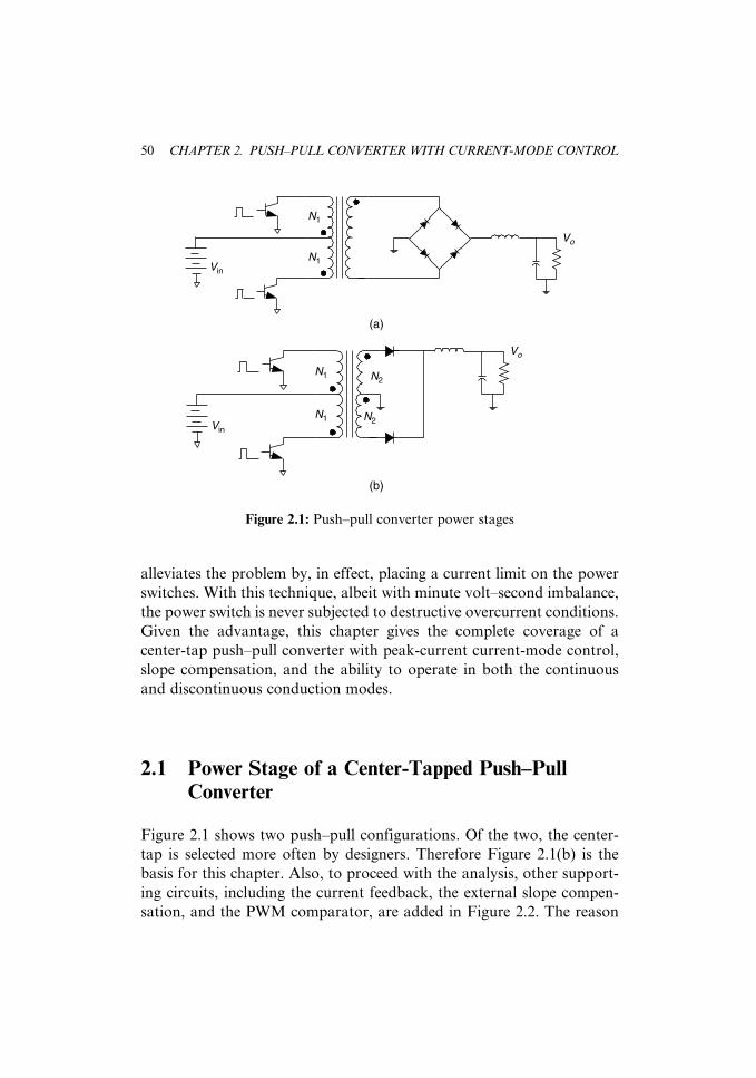
alleviates the problem by, in effect, placing a current limit on the power
switches. With this technique, albeit with minute volt–second imbalance,
the power switch is never subjected to destructive overcurrent conditions.
Given the advantage, this chapter gives the complete coverage of a
center-tap push–pull converter with peak-current current-mode control,
slope compensation, and the ability to operate in both the continuous
and discontinuous conduction modes.
2.1 Power Stage of a Center-Tapped Push–PullConverter
Figure 2.1 shows two push–pull configurations. Of the two, the center-
tap is selected more often by designers. Therefore Figure 2.1(b) is the
basis for this chapter. Also, to proceed with the analysis, other support-
ing circuits, including the current feedback, the external slope compen-
sation, and the PWM comparator, are added in Figure 2.2. The reason
Vo
N1
N1 N2
N2N1
N1Vin
(a)
Vo
Vin
(b)
Figure 2.1: Push–pull converter power stages
50 CHAPTER 2. PUSH–PULL CONVERTER WITH CURRENT-MODE CONTROL

for adding the current feedback is self-evident. As for the external slope
compensation, it is explained in a later section. Moreover, prior to the
analysis, it is beneficial to summarize the steady-state waveforms sur-
rounding the power stage. Here, two distinctive operation modes are
presented. Figure 2.3 shows the center-tap configuration in the discon-
tinuous conduction mode (DCM) while Figure 2.4 gives the more famil-
iar continuous conduction-mode (CCM) operation. Readers should have
no difficulty observing the difference between them.
2.2 Discontinuous Conduction-Mode Operation
Basically, the push–pull converters are forward-derived converters.
Many concepts and processes presented in Chapter 1 are applicable in
this instance. Among them, the selection of a minimum output filter
inductor by Equation (1.17) needs more attention. As given in the
equation, the minimum inductance required to maintain CCM operation
is inversely proportional to the minimum load current. The inductance
value, and consequently the inductor geometry, can easily become
Vo
N2
N2N1
N1
Vin
Fullwaverectifier
+
−+
−
+
−
Inputfilter
Lo
C
R19
R15C11
C1R1R3
R2
7
6
5
4
11
14
UC1856
x3
Ver
C23
R34
C22
R39
R40
RL
VAD1
D2
+VD−
d1
d2
Q1
Q2Vc
A(s)
nif iL
Figure 2.2: Push–pull converter with current-mode control
2.2. DISCONTINUOUS CONDUCTION-MODE OPERATION 51
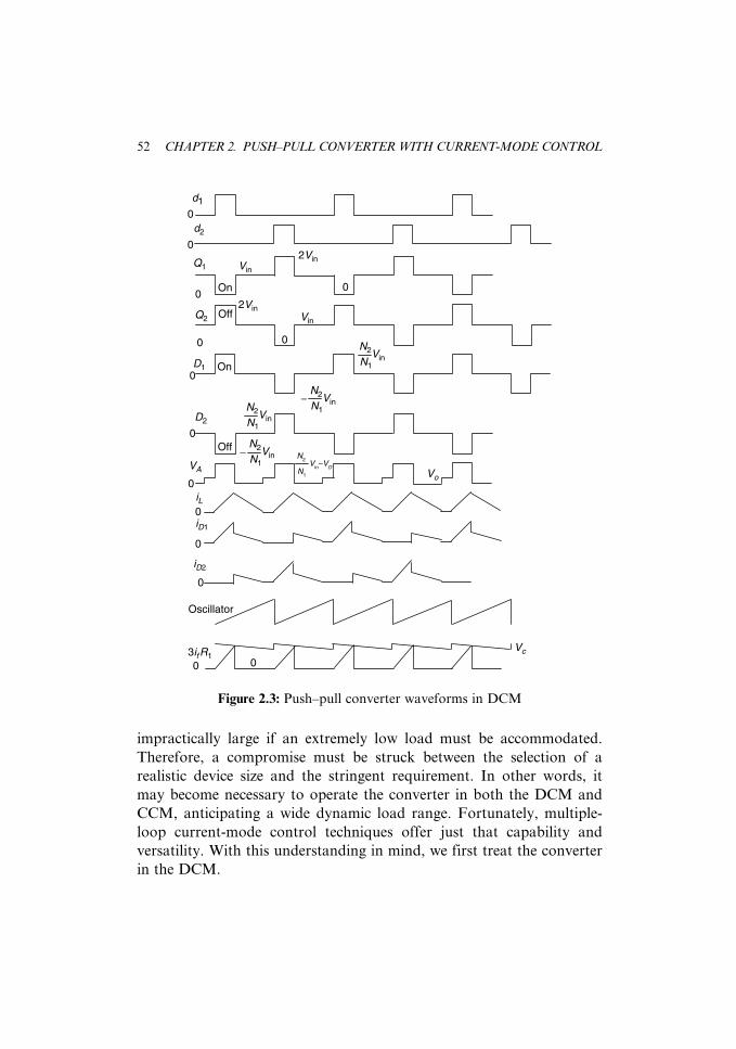
impractically large if an extremely low load must be accommodated.
Therefore, a compromise must be struck between the selection of a
realistic device size and the stringent requirement. In other words, it
may become necessary to operate the converter in both the DCM and
CCM, anticipating a wide dynamic load range. Fortunately, multiple-
loop current-mode control techniques offer just that capability and
versatility. With this understanding in mind, we first treat the converter
in the DCM.
0
0
0
0
0
0
0
0
0
0
d1
d2
Q1
Q2
D1
D2
VA
iL
iD1
iD2
Oscillator
Vc3ifR1
On
Off
On
Off
Vin
2Vin
2VinVin
0
0VinN1
N2
VinN1
N2
VinN1
N2
−
VinN1
N2
Vin−VDN1
N2−
0
0
Vo
Figure 2.3: Push–pull converter waveforms in DCM
52 CHAPTER 2. PUSH–PULL CONVERTER WITH CURRENT-MODE CONTROL
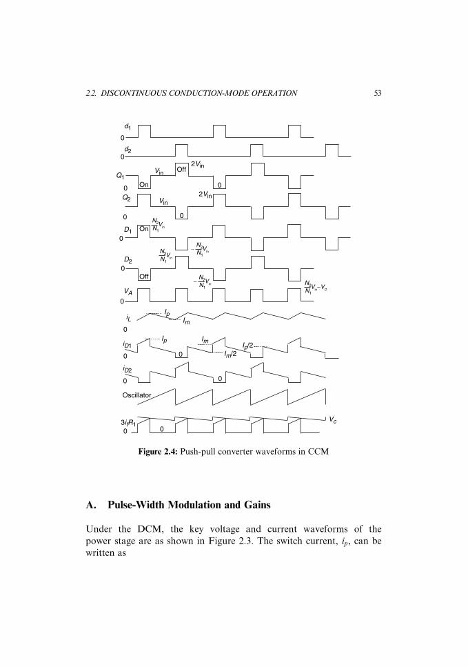
A. Pulse-Width Modulation and Gains
Under the DCM, the key voltage and current waveforms of the
power stage are as shown in Figure 2.3. The switch current, ip, can be
written as
0
0
0
0
0
0
0
0
0
0
0
d1
d2
Q1
Q2
D1
D2
VA
iL
Ip
IpIm
Im
Im/2Ip/2iD1
iD2
Vc3ifR1
Oscillator
On
On
Off
OffVin
2Vin
2VinVin
0
0
Vin−VDN1
N2Vin−
N1
N2
Vin−N1
N2
VinN1
N2
VinN1
N2
0
0
0
Figure 2.4: Push-pull converter waveforms in CCM
2.2. DISCONTINUOUS CONDUCTION-MODE OPERATION 53
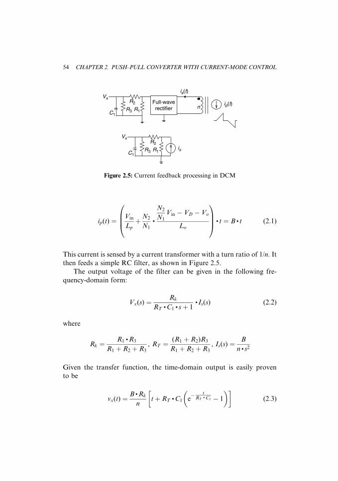
ip(t) ¼Vin
Lp
þN2
N1
.
N2
N1
Vin � VD � Vo
Lo
0BB@
1CCA . t ¼ B . t (2:1)
This current is sensed by a current transformer with a turn ratio of 1/n. It
then feeds a simple RC filter, as shown in Figure 2.5.
The output voltage of the filter can be given in the following fre-
quency-domain form:
Vx(s) ¼Rk
RT.C1 . sþ 1
. Is(s) (2:2)
where
Rk ¼R1 .R3
R1 þ R2 þ R3
, RT ¼(R1 þ R2)R3
R1 þ R2 þ R3
, Is(s) ¼B
n . s2
Given the transfer function, the time-domain output is easily proven
to be
vx(t) ¼B .Rk
ntþ RT
. C1 e� t
RT. C1 � 1
� �� �(2:3)
Full-waverectifier
R2
R2
R3
R3 R1
R1C1
C1
nip(t)
is(t)
is
Vx
Vx
Figure 2.5: Current feedback processing in DCM
54 CHAPTER 2. PUSH–PULL CONVERTER WITH CURRENT-MODE CONTROL

Next, the steady-state slope compensation output must be deter-
mined. For this, we begin by writing a differential equation for node V1
of Figure 2.6:
dV1
dtþ 1
t1
V1 ¼1
t1
Vi, t1 ¼ R15 . C11 (2:4)
where Vi is the external oscillator input, given as
Vi(t) ¼(Va þ k1 . t) 0 # t # Tu
Vb � k2 . (t� Tu) Tu # t # Ts
�(2:5)
Note that the oscillation input is periodic and, by using approaches
similar to those outlined in Chapter 1 and again invoking the concept
of continuity of state, V1 is obtained:
V1(t) ¼
v1a . e�
t
t1 þVa 1� e�
t
t1
0@
1Aþ
k1 tþ t1 e�
t
t1 � 1
0@
1A
24
35 0 # t # Tu
v1b . e�
t� Tu
t1 þVb 1� e�
t� Tu
t1
0B@
1CA� Tu # t # Ts
k2 t� Tu þ t1 e�
t� Tu
t1 � 1
0B@
1CA
264
375
8>>>>>>>>>>>>>>>>>>>>>>>>><>>>>>>>>>>>>>>>>>>>>>>>>>:
(2:6)
+
−R15
R19
C11
V1
Ver
Vn
Vea
Vi (t )
Va
Vb
Tu
Ts
k1k2
Figure 2.6: Slope-compensation processing
2.2. DISCONTINUOUS CONDUCTION-MODE OPERATION 55

where v1a and v1b are the cyclic starting states of V1 and the end result of
applying the technique of continuity of states.
Once V1 is obtained, another differential equation at the output node,
Vea, can be written
Vea(t) ¼ Ver � t3
dV1
dt, t3 ¼ R19 . C11 (2:7)
By further combining V1 and the second differential equation, the
potential at the inverting input of the PWM, TI UC1856, comparator is
then expressed as
Ver� t3
Va� v1a
t1
� �e�
t
t1 þk1 1� e�
t
t1
0@
1A
24
35� 1:2 0 # t # Tu (2:8)
The steady-state duty cycle is hence determined when the current
feedback signal intercepts the inverting input. That is, the duty cycle is
embedded in the following:
3 . vx(D . Ts) ¼ Ver � t3
Va � v1a
t1
� �e� D . Ts
t1 þ k1 1� e� t
D . Ts
t1
� �� �� 1:2 (2:9)
From this identity, a function can be defined:
f (Ver, Vin, Vo, D) ¼ 3 . vx(D . Ts)� Verþ
t3
Va � v1a
t1
� �e� D . Ts
t1 þ k1 1� e� D . Ts
t1
� �� �þ 1:2 ¼ 0 (2:10)
The preceding function then yields the small-signal gains as
Fm ¼@D
@Ver
¼ �
@f
@Ver
@f
@D
, Fv ¼@D
@Vo
¼ �
@f
@Vo
@f
@D
, Fg ¼@D
@Vin
¼ �
@f
@Vin
@f
@D
(2:11)
These gain factors aree used in Section 2.1.C.
56 CHAPTER 2. PUSH–PULL CONVERTER WITH CURRENT-MODE CONTROL
B. DC Closed Loop
As is shown in Figure 2.3, the output inductor current under DCM is a
repetitive triangle with a peak magnitude of
Ipk ¼
N2
N1
Vin � Vo
� �D
Lo . fs(2:12)
In theory, the load current equals the average value of the output
inductor current; that is,
N2
N1
Vin � Vo
� �D(DþD2)
2 . Lo. fs
¼ Vo
RL
(2:13)
Furthermore, volt–second balance also requires
N2
N1
Vin � Vo
� �D� (Vo þ VD)D2 ¼ 0 (2:14)
Both equations can be combined and rearranged. The combination
produces a quadratic equation:
a . V 2o þ b .Vo þ c ¼ 0 (2:15)
where
a ¼ 2Lo. fs
RL
, b ¼ 2Lo. fs . VD
RL
þD2 VD þN2
N1
Vin
� �,
c ¼ �N2
N1
Vin.D2 VD þ
N2
N1
Vin
� �(2:16)
That is to say, the converter main output can be expressed in terms of
the open-loop duty cycle, D, the input bus, Vin, the load, RL, and other
power stage components and parameters:
Vo ¼�bþ
ffiffiffiffiffiffiffiffiffiffiffiffiffiffiffiffiffiffiffiffiffiffiffib2 � 4 .a . cp
2 .a(2:17)
2.2. DISCONTINUOUS CONDUCTION-MODE OPERATION 57

Ideally, it would be even more desirable to express the main output in a
closed form, similar to what was done in section 1.10. However, in this
case, no solution in that form can be obtained, since (2.10) is
a transcendental equation and would not yield the duty cycle in
explicit form. This condition leaves us the remaining approach, the
numerical approximation method and loop partition outlined in section
1.6. This latter technique is performed by first redefining function
f (Ver, Vin, Vo, D) ¼ f [Ver(Rx, . . . , Vo), Vin, Vo, D] because, in almost
all cases, the feedback error voltage can be expressed as a function of
feedback circuit components, Rx, and the main output. Then the other
function, g(X , . . . , Vin, Vo, D), is also defined based on (2.17):
g(X , . . . , Vin, Vo, D) ¼ Vo ��bþ
ffiffiffiffiffiffiffiffiffiffiffiffiffiffiffiffiffiffiffiffiffiffiffib2 � 4 .a . cp
2 . a¼ 0 (2:18)
where X stands for many component values and device parameters.
Once both functions are defined, the closed-loop numerical solution
can be found by solving both simultaneously. The solution consists of the
steady-state, closed-loop duty cycle and the main output, given a load
condition RL and input voltage Vin.
In addition to the steady-state solution, the output sensitivity can be
derived by applying exactly the same process as outlined in section 1.6.
C. AC Closed Loop
Through a rather tedious procedure, the steady-state condition is estab-
lished in the previous sections. The remaining task for DCM operation is
again the AC studies. Without exception, the power stage transfer func-
tions are the main focus. We once again invoke the state-space averaged
model, Figure 2.7, that also includes isolation and input filter source
impedance Zs and transfer function H(s). The input loop gives
iis ¼
N2
N1
H(s)
N2
N1
� �2
Zs
vvin �1
N2
N1
� �2
Zs
vvg (2:19)
58 CHAPTER 2. PUSH–PULL CONVERTER WITH CURRENT-MODE CONTROL

And the input and output nodes give
�
N2
N1
� �2
Zs
r1
þ 1
0BBB@
1CCCAvvg þ
N2
N1
� �2
Zs. g1 . vvo
¼N2
N1
H(s) . vvB þN2
N1
� �2
Zs. j1 . dd, g2 . vvg �
1
r2
þ 1
RL
þ C . s
� �vvo
¼� j2 . dd (2:20)
By solving the two equations in determinant form and expanding and
grouping terms, the output is found
vvo ¼
j2
g2
N2
N1
� �2
Zs
r1
þ 1
26664
37775� j1 .
N2
N1
� �2
Zs
8>>><>>>:
9>>>=>>>;
dd þN2
N1
H(s) . vvs
1
g2
N2
N1
� �2
Zs
r1
þ 1
26664
37775 1
r2
þ 1
RL
þ C . s
� �� N2
N1
� �2
Zs. g1
(2:21)
The power stage gain functions, therefore, are
( )2 ZsN1
N2
)vinH(s)( N1
N2 r2g2vgg1vo
r1
C
j2dj1d
d
i s vovg
RL
Figure 2.7: Canonical model of a push–pull converter power stage in DCM
2.2. DISCONTINUOUS CONDUCTION-MODE OPERATION 59
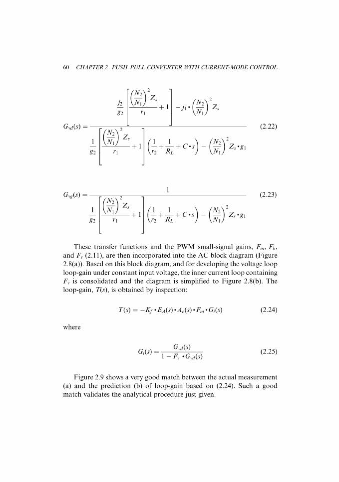
Gvd(s) ¼
j2
g2
N2
N1
� �2
Zs
r1
þ 1
26664
37775� j1 .
N2
N1
� �2
Zs
1
g2
N2
N1
� �2
Zs
r1
þ 1
26664
37775 1
r2
þ 1
RL
þ C . s
� �� N2
N1
� �2
Zs. g1
(2:22)
Gvg(s) ¼1
1
g2
N2
N1
� �2
Zs
r1
þ 1
26664
37775 1
r2
þ 1
RL
þ C . s
� �� N2
N1
� �2
Zs. g1
(2:23)
These transfer functions and the PWM small-signal gains, Fm, Fb,
and Fv (2.11), are then incorporated into the AC block diagram (Figure
2.8(a)). Based on this block diagram, and for developing the voltage loop
loop-gain under constant input voltage, the inner current loop containing
Fv is consolidated and the diagram is simplified to Figure 2.8(b). The
loop-gain, T(s), is obtained by inspection:
T(s) ¼ �Kf.EA(s) .Ae(s) . Fm
. Gi(s) (2:24)
where
Gi(s) ¼Gvd(s)
1� Fv� .Gvd(s)(2:25)
Figure 2.9 shows a very good match between the actual measurement
(a) and the prediction (b) of loop-gain based on (2.24). Such a good
match validates the analytical procedure just given.
60 CHAPTER 2. PUSH–PULL CONVERTER WITH CURRENT-MODE CONTROL

2.3 Continuous Conduction-Mode Operation
The push-pull converter possesses the capability of working in both
the DCM and the CCM. A main cause making the converter operate in
the two distinctive modes is the load current. Under a heavy load, the
converter output inductor current is understood to take the profile
shown in Figure 2.4. Obviously, significant changes take place and
the analytical treatments are expected to change as well. We therefore
follow almost the same flow as that of Chapter 1. However, some
mathematical duplication is intentionally omitted, since identical key
steps and equations have been presented.
++
+
H(s)
N2/N1
Ae(s)EA(s)
EA(s) Ae(s) Fm
Kf
++
+
vin
vover
ver
d
vo
(N2/N1)2Zs
Fg
Fm
Kf
Fv
Gvd(s)
Gvg(s)
−
(2.11) (2.22)
(2.23)(2.11)
(2.11)
(a)
(b)
+ 1 − Gvd (s) ⋅ Fv
Gvd(s)Gi (s) =
−
Figure 2.8: Push–pull converter AC block diagram in DCM
2.3. CONTINUOUS CONDUCTION-MODE OPERATION 61
(a)
(b)
100100
1 . 103 1 . 104 1 . 105−180
−135
−90
−45
−180
180
135
90
45
0
180
TdB( j )
αT( j )
100Kf ( j )
1K 10K 100K100START 100 . 000Hz STOP 100 000 . 000Hz
REF LEVEL0 . 000dB0 . 0deg
/DIV10 . 000dB45 . 000deg
MARKER 4 183 . 451HzMAG (A/R) -0 . 049dBMARKER 4 183 . 451HzPHASE (A/R) 71 . 619deg
Figure 2.9: Loop gain of a push–pull converter in DCM
62 CHAPTER 2. PUSH–PULL CONVERTER WITH CURRENT-MODE CONTROL

A. Pulse-Width Modulation and Gains
Under the CCM operation and in reference to Figure 2.4 in which
important currents associated with the power stage are clearly identified
and designated, the power switch current in a single on period can be
described as
ip(t) ¼ Aþ B . t (2:26)
where
A ¼ N2
N1
Io �VD þ Vo
2Lo
(1�D)Ts
� �,
B ¼ N2
N1
N2
N1
Vin � (VD þ Vo)
� �Lo
þ Vin
Lp
(2:27)
The primary current is processed by the same sensing circuit and yields
vx(t) ¼A . Rk
n1� e
� t
RT. C1
0@
1Aþ B .Rk
n
� tþ RT.C1 e
� t
RT. C1 � 1
0@
1A
24
35 (2:28)
Then, by exactly the same operation as in (2.9) and (2.10), the CCM
duty cycle is established by a different function:
g(ver, Vin, Vo, D) ¼ 3 . vx(D .Ts)� verþ
t3
va � v1a
t1
� �e�
D .Ts
t1 þ k1 1� e�
D . Ts
t1
0B@
1CA
264
375þ 1:2 ¼ 0
(2:29)
and so are the small-signal gains Fm, Fv, and Fg.
2.3. CONTINUOUS CONDUCTION-MODE OPERATION 63

(a)
100100
1 . 103 1 . 104 1 . 105−180
−135
−90
−45
−180
180
135
90
45
0
180
TdB( j)
αT( j)
100Kf( j )
(b)
100 1K 10K 100KSTART 100 . 000Hz STOP 100 000 . 000Hz
REF LEVEL0. 000dB0 . 0deg
/DIV10 . 000dB45 . 000deg
MARKER 9 920 . 525HzMAG (A/R) −0 . 068dBMARKER 9 920 . 525HzPHASE (A/R) 59 . 758deg
Figure 2.10: Loop gain of the push–pull converter in CCM
64 CHAPTER 2. PUSH–PULL CONVERTER WITH CURRENT-MODE CONTROL

B. DC Closed Loop
Under the CCM operation, the output voltage as a function of the open-
loop duty cycle is no different from that developed in Chapter 1, since the
push–pull converter is basically a forward converter. The open-loop
output therefore is given in the implicit function
h(X , . . . , Vin, Vo, D) ¼ Vo�N2
N1
Vin � (Rs. Dþ Rw þ Ron)
N2
N1
Vo
RL
� �Dþ VD þ Rl
Vo
RL
¼ 0 (2:30)
The closed-loop output, as in the DCM case, is hiding behind the two
functions, h(X , . . . , Vin, Vo, D) and g[ver(Rx, . . . , Vo), Vin, Vo, D].
Again, readers are cautioned that g and h are two new, implicit functions.
C. AC Closed Loop
Under the CCM, not only is the steady-state analytical form altered in
comparison with that of the DCM, but so is the AC model. Basically, the
power stage model needs a new look. However, this has all been done in
Chapter 1. We present just the end results, comparing the actual mea-
surement (a) against the theoretical prediction (b) (Figure 2.10).
2.3. CONTINUOUS CONDUCTION-MODE OPERATION 65

This page intentionally left blank

Chapter 3
Nonisolated Forward Converterwith Average Current-ModeControl
The average current-mode control, in contrast to the peak current-mode,
was claimed by Tang and Lee [3] to offer several advantages. However, in
treating the topic, many existing studies did not handle the analytical
procedure properly. This chapter gives an in-depth analysis of the sub-
ject. All discussions refer to Figure 3.1, which depicts a complete, non-
isolated forward converter using average current-mode control.
3.1 Average Current Feedback
Under CCM operation, the output filter inductor, L, current is known to
exhibit a waveform as shown in Figure 3.2.
The steady-state current feedback signal, including the sense resistor,
Ri, can be described as
Vi(t)¼Ri
. Ibþ Vg�Vo
L. t
� �¼ v1(t) 0 # t # D . Ts
Ri.
hIbþ di� Vo
L. t�D .Tsð Þ
i¼ v2(t) D . Ts # t # Ts
8<: (3:1)
67
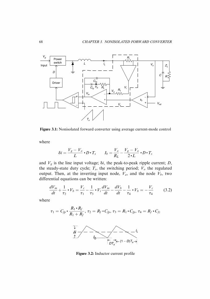
where
di ¼ Vg � Vo
L. D .Ts Ib ¼
Vo
RL
� Vg � Vo
2 . L. D . Ts
and Vg is the line input voltage; di, the peak-to-peak ripple current; D,
the steady-state duty cycle; Ts, the switching period; Vo the regulated
output. Then, at the inverting input node, Va, and the node Vb, two
differential equations can be written:
dVm
dtþ 1
t2
. Vb ¼Vc
t1
� 1
t3
. Vi
dVm
dt� dVb
dt� 1
t4
. Vb ¼ �Vc
t4
(3:2)
where
t1 ¼ Cfp.
R1 . Rf
R1 þ Rf
, t2 ¼ Rf. Cfp, t3 ¼ R1 . Cfp, t4 ¼ Rf
. Cfz
+
−+
−
R1
Rf
Cfp
Cfz
Ts
Vm
Vc+
−
Vref
RiPowerswitch
Driver
InputiL
kf
Vg
D
L
Va
ViVb
C R
ZLVo
Figure 3.1: Nonisolated forward converter using average current-mode control
(1 − D)TsDTs
IL
Ibdi
Figure 3.2: Inductor current profile
68 CHAPTER 3. NONISOLATED FORWARD CONVERTER

The equations in (3.2) are consolidated into a single one for node voltage
Vb:
dVb
dtþ vp
. Vb ¼ vx. Vc �
Vi
t3
(3:3)
where
vp ¼1
t4
þ 1
t2
, vx ¼1
t4
þ 1
t1
Equation (3.3), together with the cyclic input functions of (3.1), can
be solved for the two time segments in the steady state with the assump-
tion of two unknown, cyclic starting states, Vbx and Vby, at the beginning
of each segment. The solutions for node voltage Vb are
Vb1(t) ¼Vbx
. e�vp. t þ vx
vp
1� e�vp. tð ÞVc�
Ri. Ib
t3
B1 . tþ A1 1� e�vp. tð Þ½ �
8>><>>:
9>>=>>; . u(t) (3:4)
where
B1 ¼Vg � Vo
vp. L .
Vo
RL
� Vg � Vo
2 . L.D . Ts
� �
A1 ¼1
vp
. 1� Vg � Vo
vp. L .
Vo
RL
� Vg � Vo
2 . L. D . Ts
� �2664
3775
and
Vb2(t) ¼Vby
. e�vp. t�D . Tsð Þ þ vx
vp
1� e�vp. t�D . Tsð Þ
� �Vc�
Ri. Ib þ dið Þ
t3
B2 . t�D . Tsð Þ þ A2 1� e�vp. t�D . Tsð Þ
h in o0BB@
1CCA
. u(t�D . Ts)
(3:5)
3.1. AVERAGE CURRENT FEEDBACK 69
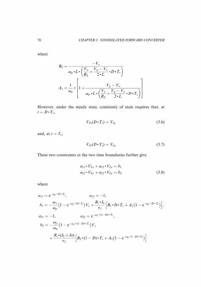
where
B2 ¼�Vo
vp. L .
Vo
RL
þ Vg � Vo
2 . L. D . Ts
� �
A2 ¼1
vp
. 1þ Vg � Vo
vp.L .
Vo
RL
þ Vg � Vo
2 .L. D .Ts
� �2664
3775
However, under the steady state, continuity of state requires that, at
t ¼ D . Ts,
Vb1(D . Ts) ¼ Vby (3:6)
and, at t ¼ Ts,
Vb1(D . Ts) ¼ Vby (3:7)
These two constraints at the two time boundaries further give
a11 . Vbx þ a12 . Vby ¼ b1
a21 . Vbx þ a22 . Vby ¼ b2 (3:8)
where
a11 ¼ e�vp. D . Ts , a12 ¼ �1,
b1 ¼ �vx
vp
1� e�vp. D . Ts
� �Vc þ
Ri. Ib
t3
hB1 . D . Ts þ A1 1� e�vp
. D . Ts� �i
,
a21 ¼ �1, a22 ¼ e�vp. (1�D) . Ts ,
b2 ¼ �vx
vp
1� e�vp. (1�D) . Ts
� �Vc
þ Ri. (Ib þ di)
t3
hB2 . (1�D) . Ts þ A2 1� e�vp
. 1�D) . Ts� �i
70 CHAPTER 3. NONISOLATED FORWARD CONVERTER
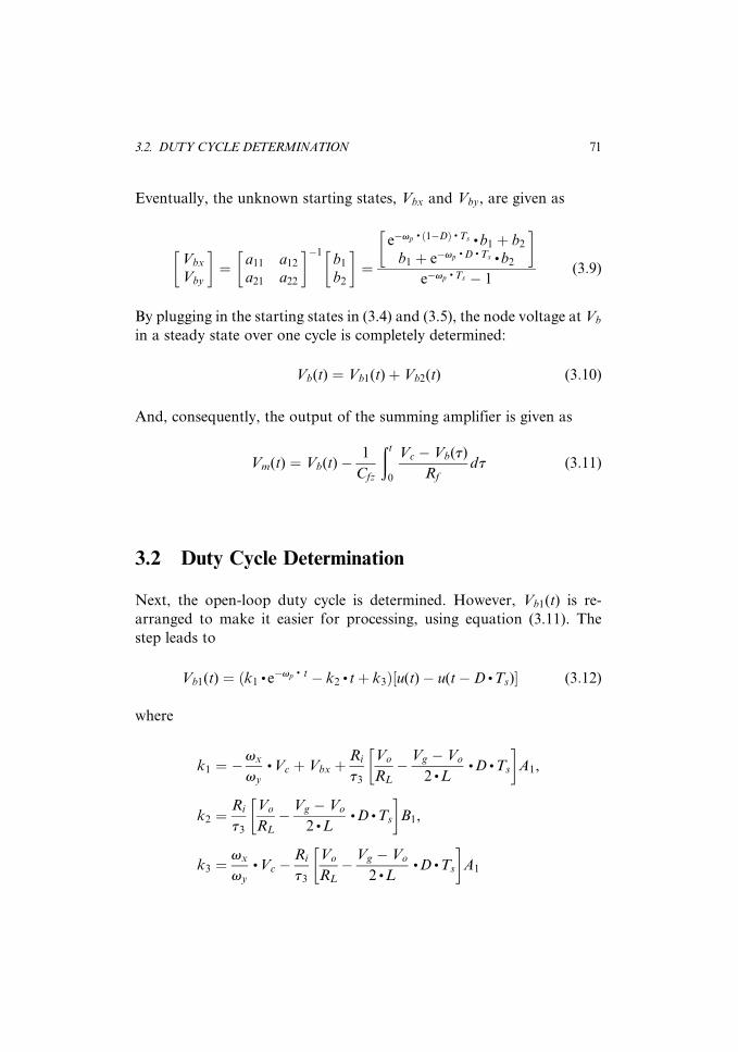
Eventually, the unknown starting states, Vbx and Vby, are given as
Vbx
Vby
� �¼ a11 a12
a21 a22
� ��1b1
b2
� �¼
e�vp. 1�Dð Þ . Ts . b1 þ b2
b1 þ e�vp. D . Ts . b2
� �e�vp
. Ts � 1(3:9)
By plugging in the starting states in (3.4) and (3.5), the node voltage at Vb
in a steady state over one cycle is completely determined:
Vb(t) ¼ Vb1(t)þ Vb2(t) (3:10)
And, consequently, the output of the summing amplifier is given as
Vm(t) ¼ Vb(t)�1
Cfz
ðt
0
Vc � Vb(t)
Rf
dt (3:11)
3.2 Duty Cycle Determination
Next, the open-loop duty cycle is determined. However, Vb1(t) is re-
arranged to make it easier for processing, using equation (3.11). The
step leads to
Vb1(t) ¼ k1 . e�vp. t � k2 . tþ k3ð Þ u(t)� u(t�D .Ts)½ � (3:12)
where
k1 ¼ �vx
vy
. Vc þ Vbx þRi
t3
Vo
RL
� Vg � Vo
2 . L. D . Ts
� �A1,
k2 ¼Ri
t3
Vo
RL
� Vg � Vo
2 . L. D . Ts
� �B1,
k3 ¼vx
vy
. Vc �Ri
t3
Vo
RL
� Vg � Vo
2 . L. D . Ts
� �A1
3.2. DUTY CYCLE DETERMINATION 71

And the corresponding summing amplifier output is given
Vm1(t) ¼ k1 . e�vpt � k2 . tþ k3 �Vc
Rf.Cfz
t
þ 1
Rf.Cfz
� k1
vp
e�vpt � 1ð Þ � k2
2t2 þ k3 . t
� �(3:13)
In general, an external sawtooth clock is also provided for PWM
operation. It is easily described as (Vos þ Set), in which Vos is the triangle
wave offset and Se is the ramp slope. The open-loop, pulsewidth-
modulated duty cycle is then determined by the intercept of the ramp
and the summing amplifier output, Vm1(t):
Vm1(Vo, Vg, Vc, D, RL, . . . ) ¼ Vos þ Se. D . Ts (3:14)
3.3 Steady-State Closed Loop
Referring to Figure 3.1, as in previous chapters, we can establish the
following two equations representing the negative feedback with an
external precision reference voltage, Vref , and high gain error amplifier,
kfb, and the power stage:
Vc ¼ kfb(Vref � Vo) (3:15)
Vo ¼ D . Vg (3:16)
It is understood that (3.14)–(3.16), when combined, constitute the closed-
loop description for the converter. However, neither the output nor the
duty cycle is given in explicit function form. Instead, the output, the
control voltage, and the duty cycle are given in implicit function
form. All three variables can be solved numerically, but they do not
offer symbolic, closed-form solutions so desired by some. It shall
also be understood that A1, B1, A2, B2, b1, b2, Vbx, Vby, k1, k2, and k3
are all functions of output Vo, source Vg, error Vc, duty cycle D, and
load RL.
72 CHAPTER 3. NONISOLATED FORWARD CONVERTER
3.4 Closed-Loop Regulation and Output Sensitivity
Power supply output, in general, is given a specified regulation range
against load and line (input) variation. It is therefore essential to know
the output sensitivity against load resistance and input change. These
performance figures are mathematically equivalent to the partial deriva-
tives @Vo=@RL and @Vo=@Vg. However, as indicated in the previous
section, the output voltage cannot be easily expressed in explicit, com-
pact closed form, and the desire to have a simple derivative is hindered.
We again employ the Jacobian determinant. First, three implicit func-
tions are defined:
f (Vo, Vg, Vc, D, RL) ¼ Vm1(Vo, Vg, Vc, D, vRL)� (Vos þ Se. D .Ts) ¼ 0
g(Vo, Vg, Vc, D, RL) ¼ Vc � kfb(Vref � Vo) ¼ 0
h(Vo, Vg, Vc, D, RL) ¼ Vo �D . Vg ¼ 0
(3:17)
The output sensitivity against input with the load held constant is given as
@Vo
@Vg
¼ �
@f =@Vg @f =@Vc @f =@D
@g=@Vg @g=@Vc @g=@D
@h=@Vg @h=@Vc @h=@D
@f =@Vo @f =@Vc @f =@D
@g=@Vo @g=@Vc @g=@D
@h=@Vo @h=@Vc @h=@D
(3:18)
By the same token, the output sensitivity against the load with input held
constant is given as
@Vo
@RL
¼ �
@f =@RL @f =@Vc @f =@D
@g=@RL @g=@Vc @g=@D
@h=@RL @h=@Vc @h=@D
@f =@Vo @f =@Vc @f =@D
@g=@Vo @g=@Vc @g=@D
@h=@Vo @h=@Vc @h=@D
(3:19)
3.4. CLOSED-LOOP REGULATION AND OUTPUT SENSITIVITY 73

Other sensitivity figures against components, of course, can be
obtained through a similar procedure, providing the associated implicit
function f (Vo, . . . ) is modified accordingly to become f (Vo, . . . , Rx, . . . ).Then, the total regulation is expressed as
ffiffiffiffiffiffiffiffiffiffiffiffiffiffiffiffiffiffiffiffiffiffiffiffiffiffiffiffiffiffiffiffiffiffiffiffiffiffiffiffiffiffiffiffiffiffiffiffiffiffiffiffiffiffiffiffiffiffiffiffiffiffiffiffiffiffiffiffiffiffiffiffiffiffiffiffiffiffiffiffiffiffiffiffiffiffiffiffiffiffiffiffiffiffiffiffiffiffiffiffiffiffiffiffiffiffi@Vo
@Vg
. dVg
� �2
þ @Vo
@RL
. dRL
� �2
þ @Vo
@Rx
. dRx
� �2
þ . . .
s(3:20)
3.5 Small-Signal Loop Gain and Stability
Given the steady state obtained so far, the examination for the con-
verter’s small-signal behavior can then proceed. The small-signal block
diagram is given in Figure 3.3.
Three important pulsewidth-modulation gains, Fm ¼ @D=@Vc,
Fvo ¼ @D=@Vo, and Fvg ¼ @D=@Vg, must be derived first. But, as can be
seen from (3.14), the duty cycle is again in implicit function form. The
single-function Jacobian determinant is therefore enlisted once more to
obtain those gain factors. They are
Fm ¼ �@f =Vc
@f =D, Fvo ¼ �
@f =Vo
@f =D, Fvg ¼ �
@f =Vg
@f =D(3:21)
+−
+
++EA(s) He(s)
vg
vo
Ri/Ls
Zf (s) = Rf Cfz ⋅ s+ + Cfp ⋅ s
−1 −11
−Zf (s)/Rl
−Zf (s)/Rl Rl/ZL
1 + [Zf (s)/Rl]+
+
Gvg
Gvd
Fvg
Fm
Fvo
vc dD
Figure 3.3: Small-signal block diagram
74 CHAPTER 3. NONISOLATED FORWARD CONVERTER

where f is the first implicit function in (3.17). The three gain factors stem
from the realization that the total differential, dD, of the duty cycle is
expressible as
dD ¼ @D
@Vc
. dVc þ@D
@Vo
. dVo þ@D
@Vg
.dVg (3:22)
Given constant source, the block diagram in Figure 3.3 can be
simplified to Figure 3.4. By absorbing the inner loop, Figure 3.4 is
reduced to a single loop (Figure 3.5). From the single-loop figure, the
loop gain is given as
T(s) ¼ EA(s) . 1þ Zf (s)
R1
� �.Fm
.Gvd
. He(s)
1þ Gvd. He(s) .Fvo
.Zf (s)
R1
. Ri
ZL
(3:23)
3.6 Example
Tang and Lee [3] give an example with Vg ¼ 14, Vo ¼ 5, R ¼ 1,
L ¼ 37:5 mH, C ¼ 380 mF, fs ¼ 50KHz, Ri ¼ 0:1, R1 ¼ 2:2 K,
+ −
++
+ He(s)
−Zf (s)/Rl Ri /ZL
Gvd
Fvo
Fm
vc dDEA(s) 1 + [Zf (s)/Rl]
Zf (s) = Rf Cfz ⋅ s+ + Cfp ⋅ s
−1 −11
vo
Figure 3.4: Simplified block diagram
+− Zf (s) ⋅
EA(s) 1 + [Zf (s)/Rl]vovc Fm
Gvd ⋅ He(s)
1 + Gvd ⋅ He(s) ⋅ Fvo
⋅ Rl ZL
Ri
Figure 3.5: Block diagram with current loop absorbed
3.6. EXAMPLE 75
Rf ¼ 30:5 K,Cfz ¼ 5:8 nF, andCfp ¼ 220 pF.Basedon the example, (3.14)
yields Figure 3.6.
The closed loop numerical solution for (3.14), (3.15), and (3.16) gives
D ¼ 0:357, Vo ¼ 5, and Vc ¼ 0:596, if a 50-KHz clock (oscillator ramp)
swinging between 1 V and 3.5 V is used.
3.7 State Transition Technique
In Chapter 1’s last section, state transition techniques were applied to
obtain the steady-state output for a buck converter, bypassing the
Laplace transform. The procedure enjoys an advantage in that the
input drive to the output filter, Figure 1.42, alternates between two
constant values that can be moved out of an (mathematical) integration
process. However, for the current treatment, the input Vi to the average
amplifier of Figure 3.1 is no longer a constant. This makes the math-
ematical process more cumbersome. We shall see how a time-varying
input raises the complexity level of the analytical treatment. Further-
more, to reduce the symbolic complexity to a manageable level, we use
the component values given in section 3.6.
−2−2
−1
ve(t)
vi(t)
vm(t)
T0 t
0
1
22
Figure 3.6: Average current-mode duty cycle determination
76 CHAPTER 3. NONISOLATED FORWARD CONVERTER

Now, based on (3.3) and (3.2), the two state equations are rewritten in
the standard matrix form:
d
dtx(t) ¼ d
dt
Vb(t)
Vm(t)
� �¼ A .x(t)þ B . E(t) (3:24)
where
A ¼�vp 0
� 1
t2
0
24
35, B ¼
�vx
1
t3
� 1
t1
1
t3
2664
3775, E(t) ¼ Vc
Vi(t)
� �(3:25)
in which all elements are defined in section 3.1. Matrix A has two
eigenvalues, l0 ¼ 0 and l1 ¼ �1:547 . 105. Following the same procedure
outlined in the last section of Chapter 1, two matrix exponentials are
expressed in polynomial form:
eA . t ¼ I þ b1(t) . A ¼1 0
0 1
" #þ b1(t) .
�vp 0
� 1
t2
0
264
375
¼1� vp
. b1(t) 0
� 1
t2
b1(t) 1
264
375 (3:26)
eA(t�t) ¼1� vp
. b1(t� t) 0
� 1
t2
b1(t� t) 1
24
35 (3:27)
where
b1(t) ¼1
l1
(el1. t � 1) (3:28)
Again, the general solution for (3.24) is given as
x(t) ¼ eA(t�t0)x(t0)þðt
t0
eA(t�t) . B .E(t)dt (3:29)
3.7. STATE TRANSITION TECHNIQUE 77

The integrant in (3.29) must be expanded as
eA(t�t) . B . E(t)
¼
[1� vp. b1(t� t)][vxVct3 � Vi(t)]
t3
� [Vct3b1(t� t)vxt1 � Vct3t2 � Vi(t)t1b1(t� t)þ Vi(t)t1t2]
t1t3t2
8>><>>:
9>>=>>;
(3:30)
During the turn-on time and assuming to ¼ 0, the inductor current is
ramping up and the input signal feeding the average amplifier is repre-
sented by v1(t) of (3.1). Equation (3.29) gives
x1(t) ¼ eA . tX1 þðt
0
eA(t�t) .B . E(t)dt
¼M1(t)X1 þM2(t) (3:31)
where
M1(t) ¼1� vp
. b1(t) 0
� 1
t2
b1(t) 1
24
35 (3:32)
M2(t)
¼
ðt
0
[1� vp. b1(t� t)] [vxVct3 � v1(t)]
t3
dt
�ðt
0
[Vct3b1(t� t)vxt1 � Vct3t2 � v1(t)t1b1(t� t)þ v1(t)t1t2]
t1t3t2
dt
8>><>>:
9>>=>>;
(3:33)
During the turn-off time, the inductor current is ramping down and
the input signal feeding the average amplifier is represented by v2(t) of
(3.1). Equation (3.29) gives
x2(t) ¼ eA(t�DTs)X2 þðt
DTs
eA(t�t) . B . E(t)dt
¼M3(t)X2 þM4(t) (3:34)
78 CHAPTER 3. NONISOLATED FORWARD CONVERTER

where
M3(t) ¼1� vp
. b1(t�DTs) 0
� 1
t2
b1(t�DTs) 1
24
35 (3:35)
M4(t)
¼
ðt
DTs
[1�vp. b1(t� t)] [vxVct3� v2(t)]
t3
dt
�ðt
DTs
[Vct3b1(t� t)vxt1�Vct3t2� v2(t)t1b1(t� t)þ v2(t)t1t2]
t1t3t2
dt
8>><>>:
9>>=>>;
(3:36)
At the steady state, the following holds:
M1(DTs)X1 þM2(DTs) ¼ X2
M3(Ts)X2 þM4(Ts) ¼ X1 (3:37)
In other words, both cyclic starting states X1 and X2 can be solved,
using (3.38). Once both are solved, the average amplifier’s steady-state
output, Vm(t), can be extracted from x1(t) and x2(t) column vectors.
The remaining procedure, similar to (3.14), (3.15), and (3.16), follows:
X1 ¼ [I �M3(Ts)M1(DTs)]�1[M3(Ts)M2(DTs)þM4(Ts)]
X2 ¼M1(DTs)X1 þM2(DTs) (3:38)
Unfortunately, in computing the matrix inverse for X1, a singular
condition occurs. Equation (3.38) fails to solve both starting state vec-
tors. The condition can be remedied by adding a very large resistor,
Ra ¼ 100 Mega-ohm, across Cfp of Figure 3.1. Not only is the trick
effective in avoiding singularity, it is also physically permissible, since
in general, the capacitor has leakage associated with it. Once this is done,
the circuit matrix of (3.25) changes slightly:
3.7. STATE TRANSITION TECHNIQUE 79

A ¼�vp � 1
t5
� 1
t2
� 1
t5
2664
3775, B ¼
vq
1
t3
vr
1
t3
2664
3775, E(t) ¼ Vc
Vi(t)
� �,
vq ¼1
t2
þ 1
t3
þ 1
t5
þ 1
t4
, vr ¼1
t2
þ 1
t3
þ 1
t5
, t5 ¼ RaCfp(3:39)
The modified matrix A now has two nonzero eigenvalues, l0 and l1. Two
time functions are then found:
b0(t) ¼
el0t l0
el1t l1
1 l0
1 l1
, b0(t) ¼
1 el0t
1 el1t
1 l0
1 l1
(3:40)
The matrix exponentials also change:
eA . t ¼ b0(t) . I þb1(t) . A¼b0(t)�vp . b1(t) �b1(t)
t5
� 1
t2
b1(t) b0(t)�b1(t)
t5
2664
3775 (3:41)
eA . (t�t) ¼b0(t� t)� vp
. b1(t� t) �b1(t� t)
t5
� 1
t2
b1(t� t) b0(t� t)� b1(t� t)
t5
2664
3775
eA(t�t) . B . E(t)¼b0(t� t)� vp
. b1(t� t) �b1(t� t)
t5
� 1
t2
b1(t� t) b0(t� t)� b1(t� t)
t5
2664
3775
.vq
1
t3
vr1t3
264
375 Vc
Vi(t)
� �(3:42)
Given the new matrix exponentials, equations (3.30) through (3.38) also
are modified. However, the expansion of the integrand, (3.42), is too
much to type in this small page. We omit it and assure readers that
80 CHAPTER 3. NONISOLATED FORWARD CONVERTER

eventually it does lead to the final solution and confirm Figure 3.6. (See
Appendix D.).
Anyway, by comparing this with the procedure given in section 3.1, it
is not clear which can be considered a more efficient algorithm. We
therefore leave it to the individual reader to pick and choose. For
higher-order systems, the approach using matrix exponentials may have
an edge over the approach using Laplace transformation.
3.7. STATE TRANSITION TECHNIQUE 81

This page intentionally left blank

Chapter 4
Phase-Shifted Full-BridgeConverter
Basic forward converters are covered in the previous chapters. All those
converters share a common trait: The duty cycle of themain switches varies
significantly depending on the input voltage level and the load demand.
Because of that, the Fourier harmonic contents of switching waveforms
also change wildly and produce an undesirable electromagnetic interfer-
ence environment and generate more local heat dissipation. The phase-
shifted full-bridge converter shown in Figure 4.1 solves a major part of the
problem by limiting the duty cycle to nearly a constant 50% for the left leg
switches, QA and QB, while providing PWM by phase shifting the right
leg switches, QC and QD, also in a near 50% duty cycle. In other words, all
switches are not pulsewidth-modulated. Instead, the transformer winding
and core volt–second are pulsewidth-modulated. Readers are referred to
Texas Instrument’s design considerations [4] for complete circuits.
Since the converter is still a buck converter in almost all aspects, we
do not duplicate previous efforts in analyzing the circuit. Instead, we
focus on the unique feature given for the first time in the circuit. As
mentioned in the figure caption, a current-doubling filter is employed. By
sharing the load current between two identical inductors and operating
the isolation transformer core truly in four quadrants (B–H), magnetic
material is efficiently utilized and the thermal environment is better
managed.
83

4.1 Power-Stage Operation
Prior to the mathematical treatment for the current doubler, we must
understand how the main circuit works. The four switches allow four
permissible states: states AD (QA and QD on), CB, AC, and BD. State AD
places Vin across the transformer, Tm, primary with the dot-end positive.
State CB reverses the primary voltage with the dot-end grounded. States
AC and BD place a short across the primary. Therefore, as far as the
transformer’s secondary side is concerned, there are three states across
Ns: positive (dot-end), zero, and negative. In a continuous operation, the
secondary state sequences through positive, zero, negative, and zero, and
the cycle repeats in rapid succession.
4.2 Current Doubler
To give a detailed study of the subject matter, the current-doubling
output circuit is redrawn as Figure 4.2 with loss elements included.
Tm
QDQB
Np
QCQA
OutD
OutC
OutB
OutATg 1
Tg 2
Tg 2
Vs
Ns D2
D1Tm
L
L
Vin
Ti
UCC3895and
supportingcircuits
CS
Ramp
+
−
Ref
Zf
ZiKf
Erroramp
Vcc
EAPVo
Figure 4.1: Phase-shifted full-bridge converter with current-doubling filter
84 CHAPTER 4. PHASE-SHIFTED FULL-BRIDGE CONVERTER

During the positive state, Figure 4.2 reduces to Figure 4.3, in which
diode D2 is conducting and carries two current components, the forward
transferring current (solid line) and the free-wheeling current (dashed line).
During the zero state, Figure 4.4 commences. In this state, both
diodes conduct in a freewheeling mode and share half the load.
During the negative state, Figure 4.2 reduces to Figure 4.5, in which
diode D1 is conducting and carries two current components, the forward
transferring current (solid line) and the freewheeling current (dashed line).
Vs
D1
D2
Figure 4.2: Current doubling filter
VsD2
Figure 4.3: Current-doubling filter in a positive state
D1
D2
Figure 4.4: Current-doubling filter in a zero state
Vs
D1
Figure 4.5: Current-doubling filter in a negative state
4.2. CURRENT DOUBLER 85

4.3 Steady-State Duty Cycle
For an in-depth mathematical analysis, Figure 4.3 is redrawn as Figure
4.6 with both the forward transferring current and the freewheeling
current given the symbolic names, i1 and i2.
As explained in section 4.1, the transformer secondary voltage, Vs,
has the form shown in Figure 4.7. Based on the concept of volt–second
balance and using the definition of oscillator time, Tosc, the following is
established for each inductor. It is noted that the freewheeling action
lasts (2 – D)Tosc, and VD stands for diode drop.
D . Tosc . Vin.Ns
Np
� (VDþVo)
� �� (VDþVo)[(1�D) .ToscþTosc]¼0 (4:1)
This equation gives the duty cycle referred to oscillator time as
D ¼ 2(VD þ Vo)
Vin.Ns
Np
(4:2)
If resistive losses are considered, (4.2) becomes
D ¼2 VD þ Vo þ 1
2
Vo
RL
r1
� �
Vin.Ns
Np
(4:3)
VsD2 r2 L2
L1 rc
RL
Vo
vC
r1
i2
i1
Figure 4.6: Current-doubling filter in a positive state, with mathematical symbols
Vs
DTosc Tosc
0
Figure 4.7: Source voltage feeding the current-doubling filter
86 CHAPTER 4. PHASE-SHIFTED FULL-BRIDGE CONVERTER

4.4 Steady-State Output Waveforms
Now, referring to Figure 4.6, we can write two (inductor) voltage-loop
equations and one (capacitor) current-node equation:
di1
dtþ r1 þ Rp
L1
i1 þRp
L1
i2 þk
L1
v ¼ Vs � VD
L1
Rp
L2
i1 þdi2
dtþ r2 þ Rp
L2
i2 þk
L2
v ¼ �VD
L2
� Rp
rc. C
i1 �Rp
rc. C
i2 þdv
dtþ 1� k
rc. C
v ¼ 0
(4:4)
where
k ¼ RL
rc þ RL
, Rp ¼rc
.RL
rc þ RL
, Vs ¼Ns
Np
Vin
During the positive state, and by taking Laplace transformation, (4.4) is
transformed to
sþ r1 þ Rp
L1
� �I1a(s)þ
Rp
L1
I2a(s)þk
L1
Va(s) ¼ I10a þVs � VD
L1 . s
Rp
L2
I1a(s) þ sþ r2 þ Rp
L2
� �I2a(s)þ
k
L2
Va(s) ¼ I20a þ�VD
L2 . s
� Rp
rc . CI1a(s)�
Rp
rc .CI2a(s)þ sþ 1� k
rc . C
� �Va(s) ¼ V0a
(4:5)
During the zero state, (4.4) is transformed to
sþ r1 þ Rp
L1
� �I1b(s)þ
Rp
L1
I2b(s)þk
L1
Vb(s) ¼ I10b þ�VD
L1 . s
� �e�D . Tosc
. s
Rp
L2
I1b(s) þ sþ r2 þ Rp
L2
� �I2b(s)þ
k
L2
Vb(s) ¼ I20b þ�VD
L2 . s
� �e�D . Tosc
. s
� Rp
rc. C
I1b(s)�Rp
rc. C
I2b(s)þ sþ 1� k
rc.C
� �Vb(s) ¼ V0b
. e�D . Tosc. s (4:6)
where I10a, I20a, V0a, I10b, I20b, and V0b are unknown starting conditions
for time interval D . Tosc and (1�D)Tosc.
4.4. STEADY-STATE OUTPUT WAVEFORMS 87
Equation set (4.5), for instance, yields the first inductor loop current
in the transformed domain:
I1a(s) ¼
I10a þVs � VD
L1 . s
Rp
L1
k
L1
I20a þ�VD
L2 . ssþ r2 þ Rp
L2
� �k
L2
V0a � Rp
rc. C
sþ 1� k
rc. C
� �
�������������
�������������D(s)
(4:7)
I1a(s) ¼
sþ r2 þ Rp
L2
� �k
L2
� Rp
rc. C
sþ 1� k
rc. C
� ���������
��������D(s)
I10a
þ
�
Rp
L1
k
L1
� Rp
rc.C
sþ 1� k
rc. C
� ���������
��������D(s)
I20a þ
Rp
L1
k
L1
sþ r2 þ Rp
L2
� �k
L2
��������
��������D(s)
V0a
þ
sþ r2þRp
L2
� �k
L2
� Rp
rc. C
sþ 1� k
rc. C
� ���������
��������L1 . s . D(s)
(Vs�VD)þ
Rp
L1
k
L1
� Rp
rc. C
sþ 1� k
rc. C
� ���������
��������L2 . s . D(s)
VD,
D(s) ¼
sþ r1 þ Rp
L1
� �Rp
L1
k
L1
Rp
L2
sþ r2 þ Rp
L2
� �k
L2
� Rp
rc. C
� Rp
rc. C
sþ 1� k
rc. C
� �
�������������
�������������(4:8)
88 CHAPTER 4. PHASE-SHIFTED FULL-BRIDGE CONVERTER

For further processing, (4.8) is rewritten with the understanding that
individual transfer functions F1(s) through F5(s) are identified in (4.8):
I1a(s) ¼ F1(s) . I10a þ F2(s) . I20a þ F3(s) . V0a þ F4(s, Vs)þ F5(s) (4:9)
With a little patience, we can carry out the same procedures for I2a(s)
and Va(s) to obtain
I2a(s) ¼ G1(s) . I10a þ G2(s) . I20a þ G3(s) . V0a þ G4(s, Vs)þ G5(s),
Va(s) ¼ H1(s) . I10a þH2(s) . I20a þH3(s) .V0a þH4(s, Vs)þH5(s)
(4:10)
Next we proceed with equation set (4.6), with the understanding
Vs ¼ 0, to obtain
I1b(s)¼ [F1(s) . I10bþF2(s) . I20bþF3(s) . V0bþF6(s, 0)þF5(s)]e�D . Tosc
. s,
I2b(s)¼ [G1(s) . I10bþG2(s) . I20bþG3(s) . V0bþG6(s, 0)þG5(s)]e�D . Tosc
. s,
Vb(s)¼ [H1(s) . I10bþH2(s) . I20bþH3(s) .V0bþH6(s, 0)þH5(s)]e�D . Tosc
. s
(4:11)
By taking the inverse Laplace transformation of (4.9), (4.10), and
(4.11), the following is established in matrix form:
i1a(t)
i2a(t)
va(t)
264
375 ¼
f1(t) f2(t) f3(t)
g1(t) g2(t) g3(t)
h1(t) h2(t) h3(t)
264
375
I10a
I20a
V0a
264
375þ
f4(t)þ f5(t)
g4(t)þ g5(t)
h4(t)þ h5(t)
264
375
8><>:
9>=>;
[u(t)� u(t�D . Tosc)] (4:12)
i1b(t)
i2b(t)
vb(t)
264
375¼
f1(t�D . Tosc) f2(t�D . Tosc) f3(t�D .Tosc)
g1(t�D . Tosc) g2(t�D . Tosc) g3(t�D . Tosc)
h1(t�D . Tosc) h2(t�D . Tosc) h3(t�D . Tosc)
264
375
I10b
I20b
V0b
264
375þ
f6(t�D .Tosc)þ f5(t�D . Tosc)
g6(t�D .Tosc)þg5(t�D .Tosc)
h6(t�D .Tosc)þh5(t�D .Tosc)
264
375
8>>>>>>>><>>>>>>>>:
9>>>>>>>>=>>>>>>>>;
[u(t�D . Tosc)�u(t�Tosc)] (4:13)
4.4. STEADY-STATE OUTPUT WAVEFORMS 89

From (4.12) at t ¼ D . Tosc, the following is true:
f1(D .Tosc) f2(D . Tosc) f3(D . Tosc)
g1(D . Tosc) g2(D .Tosc) g3(D . Tosc)
h1(D . Tosc) h2(D .Tosc) h3(D . Tosc)
264
375
I10a
I20a
V0a
264
375
þf4(D .Tosc)þ f5(D . Tosc)
g4(D .Tosc)þ g5(D . Tosc)
h4(D .Tosc)þ h5(D . Tosc)
264
375 ¼
I10b
I20b
V0b
264
375 (4:14)
That is,
A1 .
I10a
I20a
V0a
24
35þ B1 ¼
I10b
I20b
V0b
24
35 (4:15)
At t ¼ Tosc, and from (4.13), the other boundary condition is also
established:
f1(Tosc �D . Tosc) f2(Tosc �D .Tosc) f3(Tosc �D . Tosc)
g1(Tosc �D . Tosc) g2(Tosc �D . Tosc) g3(Tosc �D . Tosc)
h1(Tosc �D . Tosc) h2(Tosc �D . Tosc) h3(Tosc �D . Tosc)
264
375
I10b
I20b
V0b
264
375
þf6(Tosc �D . Tosc)þ f5(Tosc �D . Tosc)
g6(Tosc �D . Tosc)þ g5(Tosc �D . Tosc)
h6(Tosc �D . Tosc)þ h5(Tosc �D . Tosc)
264
375 ¼
I20a
I10a
V0a
264
375 (4:16)
That is,
A2
I10b
I20b
V0b
24
35þ B2 ¼
I20a
I10a
V0a
24
35 (4:17)
We substitute (4.15):
A2 A1 .
I10a
I20a
V0a
24
35þ B1
8<:
9=;þ B2 ¼
I20a
I10a
V0a
24
35 (4:18)
90 CHAPTER 4. PHASE-SHIFTED FULL-BRIDGE CONVERTER

The implication of (4.18) is that, under the steady state, all the cyclic
starting conditions I10a, I20a, V0a, I10b, I20b, and V0b can be determined.
Once all are known, the individual inductor loop current and capacitor
node voltage can be given a steady-state, one-cycle expression:
i1 1T (t)¼I10a
I20a
V0a
264
375
Tf1(t)
f2(t)
f3(t)
264
375þ f4(t)þ f5(t)
8><>:
9>=>;[u(t)� u(t�D .Tosc)]
þI10b
I20b
V0b
264
375
Tf1(t�D . Tosc)
f2(t�D . Tosc)
f3(t�D . Tosc)
264
375þ f6(t�D . Tosc)þ f5(t�D . Tosc)
8><>:
9>=>;
[u(t�D . Tosc)� u(t�Tosc)] (4:19)
i2 1T (t)¼I10a
I20a
V0a
264
375
Tg1(t)
g2(t)
g3(t)
264
375þ g4(t)þ g5(t)
8><>:
9>=>;(u(t)� u(t�D . Tosc) )
þI10b
I20b
V0b
264
375
Tg1(t�D .Tosc)
g2(t�D .Tosc)
g3(t�D .Tosc)
264
375þ g6(t�D . Tosc)þ g5(t�D . Tosc)
8><>:
9>=>;
[u(t�D .Tosc)� u(t�Tosc)] (4:20)
By the same token, the (ideal) capacitor voltage is expressed as
v(t)¼I10a
I20a
V0a
264
375
Th1(t)
h2(t)
h3(t)
264
375þh4(t)þh5(t)
8><>:
9>=>;[u(t)�u(t�D .Tosc)]
þI10b
I20b
V0b
264
375
Th1(t�D . Tosc)
h2(t�D . Tosc)
h3(t�D . Tosc)
264
375þh6(t�D . Tosc)þh5(t�D . Tosc)
8><>:
9>=>;
[u(t�D . Tosc)�u(t�Tosc)] (4:21)
However, (4.19) and (4.20) do not completely depict the cyclic nature
of inductor loop current yet, since the current periodicity encompasses two
oscillator cycles. Therefore, both inductor currents are represented by
i1(t) ¼ i1 1T (t)þ i2 1T (tþ T), i2(t) ¼ i1(t� T) (4:22)
4.4. STEADY-STATE OUTPUT WAVEFORMS 91

0 1 ⋅ 10−6 2 ⋅ 10−6 3 ⋅ 10−6 4 ⋅ 10−6
4 ⋅ T
8080 70
6050403020100
−40−30−20−10
−40
i1(t )
i2(t )
Vs(t )
io(t )
0 t
i1
i2
Vs
io = i1 + i2
Figure 4.8: Example waveforms of a current doubler
0 4 ⋅ 10−63 ⋅ 10−62 ⋅ 10−61 ⋅ 10−6
4 ⋅T
11.411.4
11.45
11.5
11.55
11.6
11.65
11.7
11.75
11.811.8
Vo(t )
0 t
0 4 ⋅ 10−63 ⋅ 10−62 ⋅ 10−61 ⋅ 10−6
4 ⋅ T0 t
00
0.025
0.05
0.075
0.1
0.13
0.15
0.18
0.20.2
pc(t )
Figure 4.9: Output voltage and capacitor power dissipation
92 CHAPTER 4. PHASE-SHIFTED FULL-BRIDGE CONVERTER

8
6
4
2
0
8
−8−8
−6
−4
−2
ic (t )
0 4 ⋅ 10−63 ⋅ 10−62 ⋅ 10−61 ⋅ 10−6
4 ⋅T0 t
Figure 4.10: Capacitor current
Again, (4.22) has periodicity of 2 . Tosc. And the output voltage is
Vo(t) ¼ Rp[i1(t)þ i2(t)]þ k . v(t) (4:23)
The AC ripple current through the capacitor is
ic(t) ¼ i1(t)þ i2(t)�Vo(t)
RL
(4:24)
As a result, the capacitor power dissipation is
pC(t) ¼ rc. i1(t)þ i2(t)�
Vo(t)
RL
� �2
(4:25)
4.5 Steady-State Output Waveforms Example
Given a design with Vin ¼ 270V, Vo ¼ 11:5 V, Io ¼ 60 amp, Np ¼ 16,
Ns ¼ 2, rc ¼ 0:003, r1 ¼ r2 ¼ 0:001, L1 ¼ L2 ¼ mH, C ¼ 10 mF, oscilla-
tor frequency ¼ 1 MHz, rectifier drop ¼ 0.5 V. The duty cycle based on
(4.3) is 0.713.Figure 4.8 shows the steady-statewaveforms.Figure 4.9 gives
the output voltage and capacitor power dissipation profile. Figure 4.10
gives the capacitor current.
4.5. STEADY-STATE OUTPUT WAVEFORMS EXAMPLE 93

This page intentionally left blank

Chapter 5
Current-Fed Push–PullConverters
All buck-derived converters presented so far share one more common
trait, the input line current pulsates if no additional input filter is incor-
porated. Coupled with the action of PWM, the pulsating current, equiva-
lent to a high di/dt, can create real problems, for instance, conducted
emission generated by AC current rushing back and forth along the input
wire/connection. The problem can be mitigated with the addition of an
input filter including a choke (inductor). Well, if that is all it takes, why
don’t we just move the output filter inductor to the input side? This is the
origin of current-fed (current-driven) converters in contrast to the volt-
age-fed (voltage-driven) converters given in Chapters 1–4.
In Figure 5.1, we show four current-fed converters. But we focus our
attention on only 5.1(a).
Again, as in the case of voltage-fed push–pull converters, the clock
frequency runs at twice the frequency both switches are subjected to.
Then, because of the selection of the serial input inductor and permissible
duty cycle range, all four topologies have four operating modes. Based on
the switch frequency (one-half the clock frequency), switch duty cycle, D,
defined as the ratio of switch on-time to the switch period Ts( ¼ 2Tosc) can
be larger or smaller than 50%. Operations with a larger than 50% steady-
state duty cycle are considered in an overlapping mode, whereas those in a
smaller than 50% cycle are in a nonoverlapping mode. In addition, the
95

Vo
Vo
Vo
Vo
Io
Io
Io
Io
N2
N2
N2
N2
N1
N1
N1
Q2
Q2
Q2
Q2
Q1
Q1
Q1
Q1
N1
vin
vin
vin
vin
Ns
Ns
Ns
Ns
Ns
Ns
D1
D2
D2
D2
D2
D1
D1
D1
DC
DC
DC
DC
Np
Np
Np
Np
Np
Np
Np
Np
(a)
(b)
(c)
(d)
Figure 5.1: Current-fed converters
96 CHAPTER 5. CURRENT-FED PUSH–PULL CONVERTERS

instantaneous inductor current may exhibit two cases: continuous con-
duction and discontinuous conduction. Continuous conduction is char-
acterized by an inductor current that never runs dry, while discontinuous
conduction dwells in a zero inductor current state for a definite time
duration. As a consequence, the four modes of operations are overlapping
continuous conduction, overlapping discontinuous conduction, nonover-
lapping continuous conduction, and nonoverlapping discontinuous con-
duction. Due to limitations of size, we give extensive coverage to only
overlapping continuous conduction and nonoverlapping continuous con-
duction. Readers can treat the other operating modes and configurations
following the same procedure outlined in the following.
5.1 Overlapping Continuous-Conduction Mode
This operating mode is understood to alternate between two structures,
as shown in Figure 5.2.
Io
IoVo
is
is
Ns
NsNp
Np
ip
Q2N2
N1
Q1Vin
iD 1
iD1
iD 2
ip
Np
Np
iD 2
(a)
D2Q1
Q2N2
N1
Vin
Ns
Ns
Vo + VD
VQ
Vo + VD(Vo + VD)Ns
Np
+
+
+
+
(b)
Figure 5.2: Current-fed converter with overlapping continuous conduction
5.1. OVERLAPPING CONTINUOUS-CONDUCTION MODE 97

The dwell time in Figure 5.2(a), in which both switches are on, is
(D� 0:5)Ts if the oscillator period is used as the time base. Then, the
other dwell time is (1�D)Ts in which only one switch is on. While in
(D� 0:5)Ts, a short is placed across the transformer primary. Input Vin is
impressed across LN1. During (1�D)Ts, the output Vo is reflected across
one half primary. The volt–second balance requirement across LN1 gives
(Vin�VQ)(D�0:5)Tsþ Vin�Np
Ns
(VoþVD)�VQ
� �(1�D)Ts ¼ 0 (5:1)
This leads to the open-loop duty cycle:
D ¼ 1� Ns. (Vin � VQ)
2 . Np. (Vo þ VD)
(5:2)
The input inductor, identified as ip or iL, and the output side rectifiers are
also understood to carry continuous pulsating currents as shown in
Figure 5.3.
From the output-current, is, waveform, the following is established:
IM ¼Io
2(1�D)(5:3)
From the primary-side-current, ip, waveform, the ramp-down decrement
dip, during (1�D)Ts is given by the volt–second changes divided by
inductance:
dip ¼
Np
Ns
(Vo þ VD)� Vin þ VQ
� �(1�D)Ts
LN1
(5:4)
0
0
0
0
i2
iD 1
iD 2
ip
(1 − D)Ts
Tosc
(D − 0.5)TsIxIy
IoIM
dip
Figure 5.3: Current waveforms
98 CHAPTER 5. CURRENT-FED PUSH–PULL CONVERTERS

Ampere’s law dictates that
dis ¼Np
Ns
dip ¼Np
Ns
.
Np
Ns
(Vo þ VD)� Vin þ VQ
� �(1�D)Ts
LN1
(5:5)
The secondary side’s current extreme values are
Ix¼IMþdis
2
¼ Io
2(1�D)þ Np
2Ns
.
Np
Ns
(VoþVD)�VinþVQ
� �(1�D)Ts
LN1
(5:6)
Iy ¼ IM �dis
2¼ Io
2(1�D)� Np
2Ns
.
Np
Ns
(Vo þ VD)� Vin þ VQ
� �(1�D)Ts
LN1
The primary-side current peak and trough are given:
IN1 max ¼Ns
Np
Ix
¼ Ns
Np
Io
2(1�D)þ
Np
Ns
(Vo þVD)�Vin þVQ
� �(1�D)Ts
2 . LN1
(5:7)
IN1 min ¼Ns
Np
Iy ¼Ns
Np
Io
2(1�D)�
Np
Ns
(Vo þ VD)� Vin þ VQ
� �(1�D)Ts
2 .LN1
Equations (5.7) are rewritten; for instance, the first is rewritten as
IN1 max ¼Po(Vo þ VD)
Vo(Vin � VQ)þ (Vin � VQ)Ts
4 . LN1
1�Ns(Vin � VQ)
Np(Vo þ VD)
� �(5:8)
From Figure 5.2(b), the output rectifier sees a peak inverse voltage, PIV:
PIVD1 ¼ 2Vo þ VD (5:9)
5.1. OVERLAPPING CONTINUOUS-CONDUCTION MODE 99

while the input choke clamping diode sees
PIVDC ¼N2
N1
(Vin � VQ)þ Vo (5:10)
From (5.2),
Vo ¼Ns
. (Vin � VQ)
2 .Np. (1�D)
� VD (5:11)
As a result, we obtain the power stage gain:
@Vo
@D¼ 2Np . (Vo þ VD)2
Ns. (Vin � VQ)
(5:12)
One more step establishes the critical inductance required to maintain
continuous conduction mode: that is,
IN1 min ¼Po(Vo þ VD)
Vo(Vin � VQ)� (Vin � VQ)Ts
4 . LN1 cri
1�Ns(Vin � VQ)
Np(Vo þ VD)
� �¼ 0
LN1 cri ¼Vo(Vin � VQ)2Ts
4Po(Vo þ VD)1�Ns(Vin � VQ)
Np(Vo þ VD)
� � (5:13)
Also, in order to ensure overlapping mode of operation, the duty cycle
must be larger than 50%. Therefore,
D ¼ 1� Ns. (Vin � VQ)
2 . Np. (Vo þ VD)
$ 0:5 (5:14)
And the constraint leads to the transformer’s turn ratio:
Np
Ns
$Vin � VQ
Vo þ VD
(5:15)
Figure 5.2(b) also clearly shows the minimum breakdown voltage rating
for both switches.
100 CHAPTER 5. CURRENT-FED PUSH–PULL CONVERTERS

5.2 Overlapping Continuous Conduction, Steady State
For steady-state time-domain studies, Figure 5.2 can be translated into
the equivalent circuits in Figure 5.4, which correspond to the two alter-
nating dwell times. When both switches are on, Figure 5.4(a), two
equations, one voltage loop, and one current node can be established,
describing the circuit behavior:
di1
dtþ rL
Li1 ¼
Vin � VQ
L,
dv1
dt¼ � 1
(rC þ RL)Cv1 (5:16)
When only one switch is on, as in Figure 5.4(b), and by reflecting the
primary circuit to the secondary side, a second set of differential equa-
tions is given:
di2
dtþ rL þ n2 . Rp
Li2 þ
n . kr
Lv2 ¼
Vin � VQ
L
� n . Rp
rC.C
i2 þdv2
dtþ 1� kr
rC. C
v2 ¼ 0
(5:17)
where
kr ¼RL
rC þ RL
, Rp ¼rC
. RL
rC þ RL
Vo
Vo
RL
RL
rC
rC
C
C
v1
v2
i1
ni2
vin
rLL
(a)
(b)
rL/n 2 L /n
2
(Vin − VQ)/n Ns
Npn =
Figure 5.4: Current-fed converter with overlapping continuous conduction
5.2. OVERLAPPING CONTINUOUS CONDUCTION, STEADY STATE 101

Taking a Laplace transformation of (5.16) and solving both trans-
formed equations yields
I1(s) ¼I10
sþ rL
L
� �þ Vin � VQ
L . s . sþ rL
L
� � ,
V1(s) ¼V10
sþ 1
(rC þ RL)C
(5:18)
where I10 and V10 are unknown starting states yet to be found.
The inverse Laplace transform of (5.18), employing a matrix form,
leads us to
i1(t)
v1(t)
� �¼ f1(t) 0
0 g2(t)
� �I10
V10
� �þ f3(t)
0
� �� �{u(t)�u[t�(D�0:5)Ts]} (5:19)
The same procedure is applied to (5.17):
sþ rL þ n2 . Rp
L
� �I2(s)þ
n . kr
LV2(s)
¼ I20 þVin � VQ
L . s
� �e�(D�0:5)Ts
. s,
� n .Rp
rC. C
I2(s)þ sþ 1� kr
rC. C
� �V2(s) ¼ V20e
�(D�0:5)Ts. s, (5:20)
I2(s)¼sþ1�kr
rC. C
� �De(s)
I20þ�n . kr
LDe(s)
V20þ(Vin�VQ) sþ1�kr
rC. C
� �L . s .De(s)
2664
3775e�(D�0:5)Ts
. s,
V2(s)¼
n . Rp
rC. C
De(s)I20þ
sþrLþn2 . Rp
LDe(s)
V20þ(Vin�VQ)
n . Rp
rC. C
L . s . De(s)
2664
3775e�(D�0:5)Ts
. s
(5:21)
102 CHAPTER 5. CURRENT-FED PUSH–PULL CONVERTERS

where the denominator function is
De(s) ¼sþ rL þ n2 . Rp
L
� �n . kr
L
� n . Rp
rC.C
sþ 1� kr
rC.C
� �
Taking an inverse Laplace transform of (5.21) and placing it in matrix
form, we get
i2(t)
v2(t)
� �¼
h1[t� (D�0:5)Ts] h2[t� (D�0:5)Ts
p1[t� (D�0:5)Ts] p2[t� (D�0:5)Ts]
� �I20
V20
� �
þh3[t� (D�0:5)Ts]
p3[t� (D�0:5)Ts]
� �8>>><>>>:
9>>>=>>>;
{u[t� (D�0:5)Ts]�u[t�Ts]} (5:22)
Equation (5.19) is evaluated at time boundary t ¼ (D� 0:5)Ts:
i1[(D�0:5)Ts]
v1[(D�0:5)Ts]
� �¼
f1[(D�0:5)Ts] 0
0 g2[(D�0:5)Ts]
� �I10
V10
� �þ
f3[(D�0:5)Ts]
0
� �X2¼A1 . X1þB1 (5:23)
Equation (5.22) is evaluated at time boundary t ¼ Ts=2, and we consider
the continuity of states:
i2Ts
2
� �
v2
Ts
2
� �26664
37775 ¼ h1[(1�D)Ts] h2[(1�D)Ts]
p1[(1�D)Ts] p2[(1�D)Ts]
� �I20
V20
� �þ
h3[(1�D)Ts]
p3[(1�D)Ts]
� �
A2 .X2 þ B2 ¼ X1 (5:24)
The unknown starting states are solved
X1 ¼ (I � A2 . A1)�1(A2 . B1 þ B2)
X2 ¼ A2 .X1 þ B1 (5:25)
Equations (5.19) and (5.22) then give the complete description of the
circuit under a steady state.
5.2. OVERLAPPING CONTINUOUS CONDUCTION, STEADY STATE 103
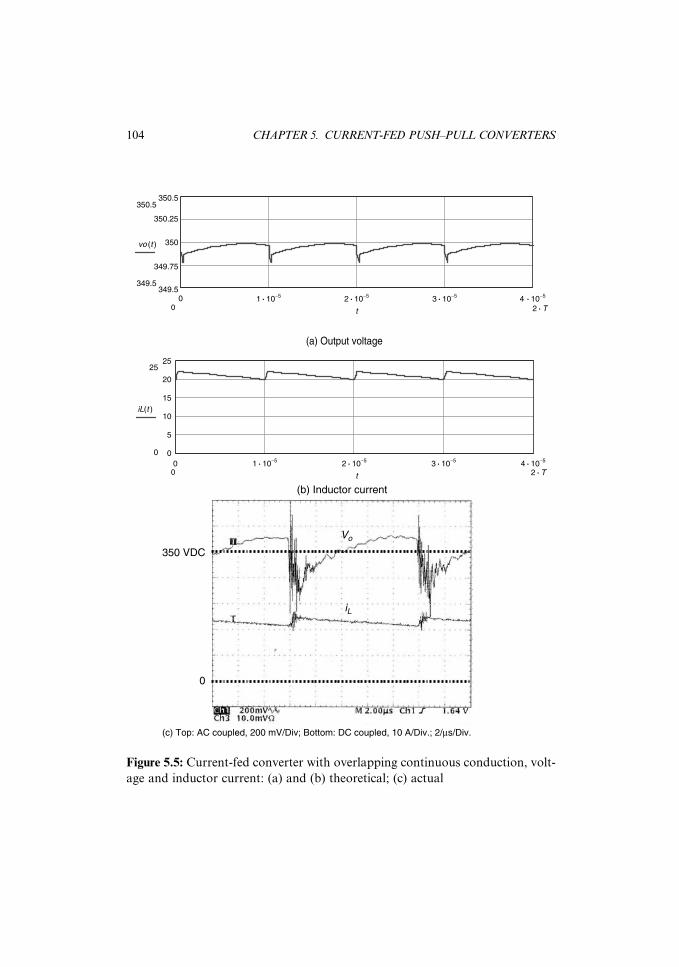
0 1 ⋅ 10−5 2 ⋅ 10−5 3 ⋅ 10−5 4 ⋅ 10−5
2 ⋅ T
2 ⋅ T
350.5350.5
350.25
350
349.75
349.5349.5
vo (t )
0 t
0 1 ⋅ 10−5 2 ⋅ 10−5 3 ⋅ 10−5 4 ⋅ 10−5
0 t
(a) Output voltage
0
5
10
15
20
2525
0
iL(t )
(b) Inductor current
(c) Top: AC coupled, 200 mV/Div; Bottom: DC coupled, 10 A/Div.; 2/µs/Div.
350 VDC
0
Vo
iL
Figure 5.5: Current-fed converter with overlapping continuous conduction, volt-
age and inductor current: (a) and (b) theoretical; (c) actual
104 CHAPTER 5. CURRENT-FED PUSH–PULL CONVERTERS

5.3 Overlapping Continuous Conduction, Example
Given a design using the configuration in Figure 5.1(c)—Np ¼ 9, Ns ¼ 44,
Vin ¼ 70, Vo ¼ 350, L ¼ 8:5 mH, rL ¼ 0:005, C ¼ 10 mF, rC ¼ 0:02,
Pout ¼ 1:46KW, VQ ¼ 0:2, VD(Schottkydiodes) ¼ 0:5, and fs ¼ 50KHz
(fosc ¼ 100KHz)—the output voltage vo and the inductor current iL are
given by Figure 5.5. The switch and transformer secondary currents
are given by Figure 5.6.
5.4 Nonoverlapping Continuous-Conduction Mode
In the case of nonoverlapping continuous-conduction operation, two
alternating topologies exist: one switch on and two switches off. The
dwell time for one switch on is DTs, and while for two switches off it is
(0:5�D)Ts. Clearly, the switch duty cycle on the basis of 2Tosc must be
less than 50%; otherwise, the factor (0:5�D) is negative. Figure 5.7
shows the two alternating configurations of the converter cycles through
repeated use in normal operation. During the dwell time DTs, one switch
and one rectifier are conducting. During the dwell time (0:5�D)Ts,
diode Dc and both rectifiers are conducting. All currents, inductor,
energy recovery, and rectifiers are understood to look like those in
Figure 5.8.
Again, the application of conservation of flux linkage gives
Vin �Np
Ns
(Vo þ VD)� VQ
� �D .Ts ¼
N1
N2
(Vo þ VD)(0:5�D)Ts (5:26)
which leads to the open-loop duty cycle:
D ¼
N1
N2
(Vo þ VD)
2 Vin þN1
N2
�Np
Ns
� �(Vo þ VD)� VQ
� � (5:27)
5.4. NONOVERLAPPING CONTINUOUS-CONDUCTION MODE 105
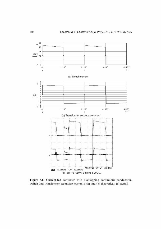
0 4 ⋅ 10−53 ⋅10−52 ⋅ 10−51 ⋅ 10−500
5
10
15
20
2525
iQ1(t )
0 t
0 4 ⋅10−53 ⋅10−52 ⋅ 10−51 ⋅ 10−5
2 ⋅ T
2 ⋅T
0 t
(a) Switch current
−6−6−5−4−3−2−1
66 5
43210is(t )
(b) Transformer secondary current
0
0
iQ1
isec
(c) Top: 10 A/Div.; Bottom: 5 A/Div.
Figure 5.6: Current-fed converter with overlapping continuous conduction,
switch and transformer secondary currents: (a) and (b) theoretical; (c) actual
106 CHAPTER 5. CURRENT-FED PUSH–PULL CONVERTERS

From the current waveforms, the DC load current Io can be expressed
as the sum of the averaged iN2 and the averaged rectifier currents iD1
and iD2:
Vo
Vo
Io
is
Ns
NsNp
Np
ip
is
iD 1Np
Npip
iD 2
VQ D2Q1
Q1
Q2N2
N1
Vin
Q2N2
N1
Vin
Ns
Ns
Vo+VD
Vo + VD(Vo + VD)Np
Ns
+
+
+
+
(a)
(b)
Figure 5.7: Current-fed converter with nonoverlapping continuous conduction
0
0
0
0
ip (or iN1)Ix
Io
Iydip
DTs
TosciN2
iD2
iD1
Ts
is
0
Figure 5.8: Current waveforms for nonoverlapping continuous conduction
5.4. NONOVERLAPPING CONTINUOUS-CONDUCTION MODE 107

< iN2 > ¼N1
N2
(Ix þ Iy)(0:5�D)
< iD1 þ iD2 > ¼Np
Ns
(Ix þ Iy)D
N1
N2
(0:5�D)þNp
Ns
D
� �(Ix þ Iy) ¼ Io
Ix þ Iy ¼Io
N1
N2
(0:5�D)þNp
Ns
D
(5:28)
The ripple current, dip, is given by
Iy � Ix ¼Vin �
Np
Ns
(Vo þ VD)� VQ
� �D . Ts
LN1
(5:29)
We can follow the procedure of (5.6) to (5.14) and obtain the PIV for
switches, PIV for rectifiers, open-loop output, output gain, and critical
inductance. However, there is no point repeating those steps, and we go
to the next important topic.
5.5 Load Current Sharing and Parallel Operation
The current-fed converters possess one very desirable quality all con-
verters presented so far lack. By having an input inductor but no output
inductor, not only is the input current made nonpulsating, the output
behaves effectively as a current-source-feeding load impedance shared by
other identical current-fed converters. In other words, we can place
multiple current-fed converters in parallel, feeding one common load
such that the load current is almost equally shared among converters.
We use Figures 5.9 and 5.10 to discuss this important subject: current
sharing. We begin with Figure 5.9.
Figure 5.9 intentionally omits showing the output load impedance,
since that is to be shared by other units. In this figure, the output is a
current source. But it is to be understood that the voltage feedback is
108 CHAPTER 5. CURRENT-FED PUSH–PULL CONVERTERS
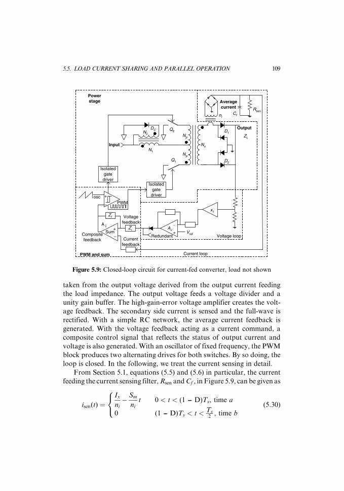
taken from the output voltage derived from the output current feeding
the load impedance. The output voltage feeds a voltage divider and a
unity gain buffer. The high-gain-error voltage amplifier creates the volt-
age feedback. The secondary side current is sensed and the full-wave is
rectified. With a simple RC network, the average current feedback is
generated. With the voltage feedback acting as a current command, a
composite control signal that reflects the status of output current and
voltage is also generated. With an oscillator of fixed frequency, the PWM
block produces two alternating drives for both switches. By so doing, the
loop is closed. In the following, we treat the current sensing in detail.
From Section 5.1, equations (5.5) and (5.6) in particular, the current
feeding the current sensing filter, Rsen and Cf , in Figure 5.9, can be given as
isen(t) ¼Ix
ni
� Sm
ni
t 0 < t < (1 --- D)Ts, time a
0 (1 --- D)Ts < t < Ts2
, time b
8<: (5:30)
N2
N1
Q2
Q1 D2
D1
Ns
ZL
Cfni
DC
Np
Np
+
−Vref
x1
+
−
+
−
oscPWM
PWM and sum
SumRedundant
Output
Input
Rsen
Zf
Zi Av
A i
Powerstage
Isolatedgatedriver
Isolatedgatedriver
Voltagefeedback
Compositefeedback Current
feedback
Current loop
Voltage loop
Averagecurrent
Figure 5.9: Closed-loop circuit for current-fed converter, load not shown
5.5. LOAD CURRENT SHARING AND PARALLEL OPERATION 109

where Ix is given by (5.6), ni is the current transformer, and the slope is
Sm ¼Np
Ns
.
Np
Ns
(Vo þ VD)� Vin þ VQ
� �LN1
(5:31)
At the output node of the current-sensing, full-wave rectifier, the
following is established for the voltage across the RsenCf filter:
dv
dtþ v
RsenCf
¼ dv
dtþ v
t¼ isen(t)
Cf
(5:32)
Taking a Laplace transform and considering the two cyclic time
intervals given in (5.30), the following is further established:
Va(s)
Vb(s)
� �¼
1
sþ 1
t
V0a þ1
Cf
Ix
ni
.1
s sþ 1
t
� �� Sm
ni
.1
s2 sþ 1
t
� �2664
3775, time a
1
sþ 1
t
e�1(1�D)T . ssV0b, time b
8>>>>>>>><>>>>>>>>:
9>>>>>>>>=>>>>>>>>;
(5:33)
Inverse Laplace transformation gives
va(t)
vb(t)
� �¼ e�t=tV0a þ
1
Cf
[f1(t)� f2(t)], time a
e�[t�(1�D)Ts]=tV0b, time b
8<:
9=; (5:34)
Boundary conditions and the requirement of continuity of states gives
e�[(1�D)Ts]=tV0a � V0b ¼�1
Cf
{f1[(1�D)Ts]� f2[(1�D)Ts]}
� V0a þ e�[(1�D)Ts]=tV0b ¼ 0
(5:35)
Equation (5.35) yields the cyclic starting states, V0a and V0b, and the
current sensor output voltage is completely determined. For example,
110 CHAPTER 5. CURRENT-FED PUSH–PULL CONVERTERS
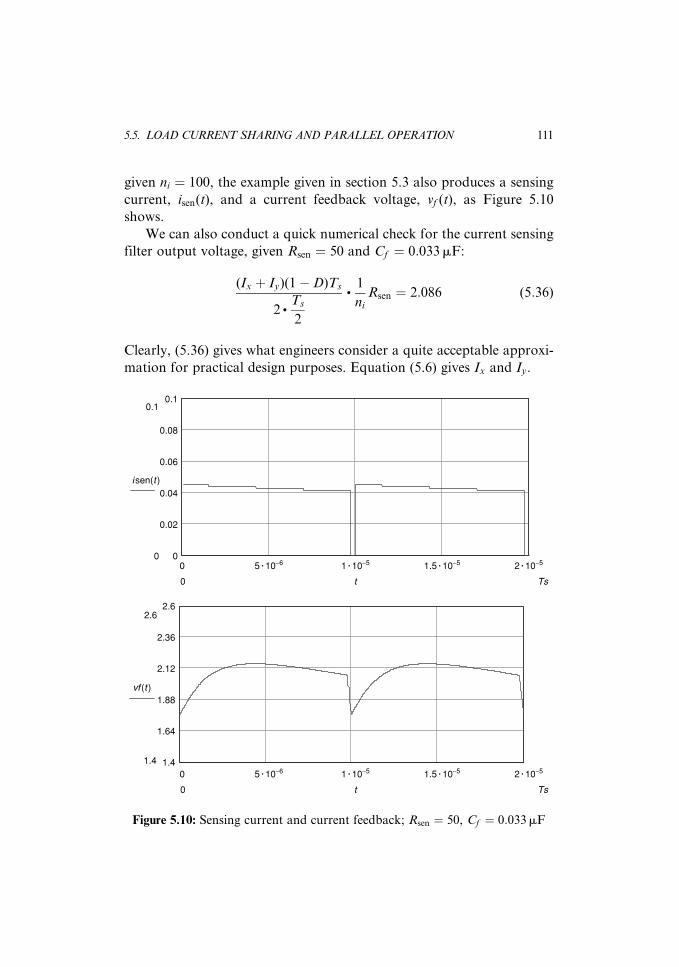
given ni ¼ 100, the example given in section 5.3 also produces a sensing
current, isen(t), and a current feedback voltage, vf (t), as Figure 5.10
shows.
We can also conduct a quick numerical check for the current sensing
filter output voltage, given Rsen ¼ 50 and Cf ¼ 0:033 mF:
(Ix þ Iy)(1�D)Ts
2 .Ts
2
.1
ni
Rsen ¼ 2:086 (5:36)
Clearly, (5.36) gives what engineers consider a quite acceptable approxi-
mation for practical design purposes. Equation (5.6) gives Ix and Iy.
0 5 .
10−6 1 .
10−5 1.5 .
10−5 2 .
10−500
0.02
0.04
0.06
0.08
0.10.1
i sen(t )
Ts0 t
0 5 .
10−6 1 .
10−5 1.5 .
10−5 2 .
10−5
Ts0 t
1.41.4
1.64
1.88
2.12
2.36
2.62.6
vf (t )
Figure 5.10: Sensing current and current feedback; Rsen ¼ 50, Cf ¼ 0:033 mF
5.5. LOAD CURRENT SHARING AND PARALLEL OPERATION 111
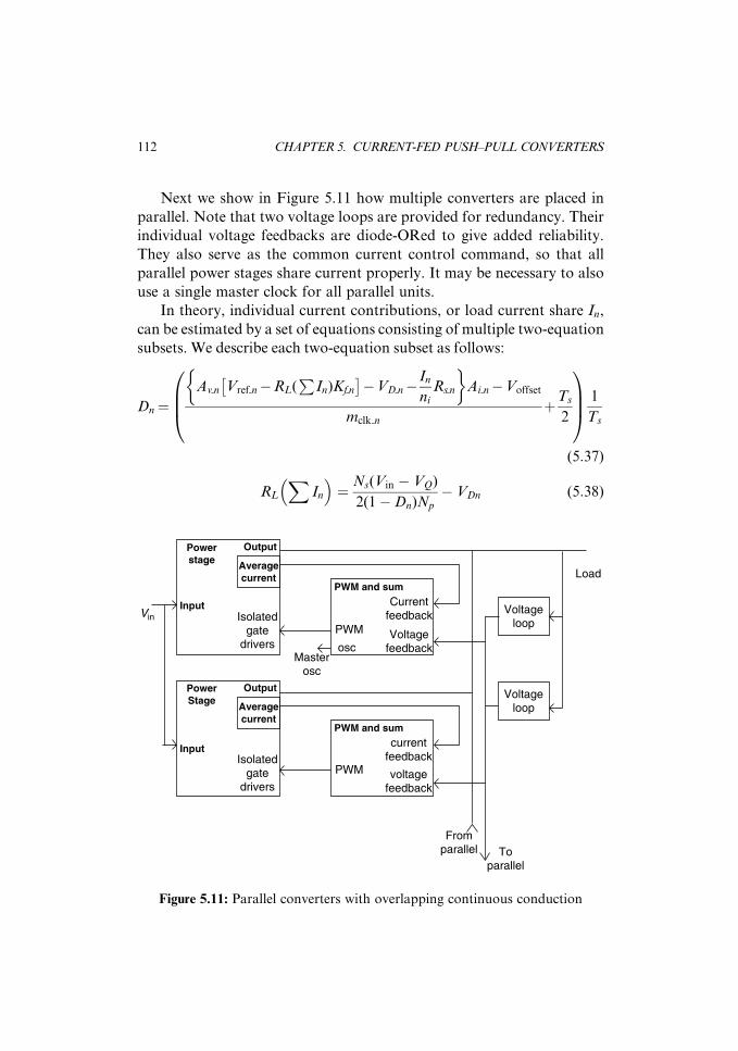
Next we show in Figure 5.11 how multiple converters are placed in
parallel. Note that two voltage loops are provided for redundancy. Their
individual voltage feedbacks are diode-ORed to give added reliability.
They also serve as the common current control command, so that all
parallel power stages share current properly. It may be necessary to also
use a single master clock for all parallel units.
In theory, individual current contributions, or load current share In,
can be estimated by a set of equations consisting of multiple two-equation
subsets. We describe each two-equation subset as follows:
Dn¼Av n Vref n�RL(
PIn)Kfn
��VD n�
In
ni
Rs n
� �Ai n�Voffset
mclk n
þTs
2
0BB@
1CCA 1
Ts
(5:37)
RL
XIn
� �¼ Ns(Vin � VQ)
2(1�Dn)Np
� VDn (5:38)
PWM and sum
PWM and sum
PWM
PWM
Output
Output
Input
Input
Load
Vin
osc
Powerstage
PowerStage
Averagecurrent
Averagecurrent
Isolatedgate
drivers
Isolatedgate
drivers
Masterosc
Currentfeedback
currentfeedback
Voltagefeedback
voltagefeedback
Voltageloop
Voltageloop
Toparallel
Fromparallel
Figure 5.11: Parallel converters with overlapping continuous conduction
112 CHAPTER 5. CURRENT-FED PUSH–PULL CONVERTERS

where the subscript n stands for parallel module count, Av is voltage error
amplifier gain, Vref is precision reference, RL is load, Kf is voltage
feedback ratio, VD is diode drop, Rs is current sensor, Ai is current
error amplifier gain, Voffset is oscillator trough voltage, mclk is oscillator
ramp-up slope, and D is duty cycle. For a nonoverlapping operating
mode, (5.37) must be modified.
5.6 AC Small-Signal Studies Using State-SpaceAveraging
The state-space average technique was conceived in the 1970s by Robert
Middlebrook and Slobodan Cuk [1]. In this section, we use the technique
for Figure 5.1(a) with a minor modification and in a nonoverlapping
continuous-conduction mode. The modification is that diode Dc is fed
back to the input. In the meantime, two subtopologies for a nonoverlap-
ping operation correspond to one switch on and both switches off. Figure
5.12 shows the equivalent circuits. Many parasitic components are also
included: inductor series resistance rL, primary winding resistance rp,
secondary winding resistance rs, capacitor series resistance re, and Lmp
for primary magnetizing inductance. From Figure 5.12(a), equations
(5.39) are established with the secondary circuit reflected to the primary
side:
C/n 2
nv
n 2rs
rs
n 2re
re
n 2RL
RL
nvo
vo
sp
NN
n =
L1 i1 i2
L2
Lmp
L ms
(a) One switch on
C
vVin
Vin
rL2
rL1 rp
(N1/N2)i1 ni2
(b) Both switches off
Figure 5.12: Equivalent circuits, nonoverlapping continuous conduction
5.6. AC SMALL-SIGNAL STUDIES USING STATE-SPACE AVERAGING 113

d
dt
i1
i2
v
26643775¼ d
dtX1¼
rL1þrpþn2(rsþRp)
L1
n2(rsþRp)
L1
�k . n
L1
n2(rsþRp)
Lmp
n2(rsþRp)
Lmp
k . n
Lmp
n . Rp
re. C
�n . Rp
re. C
�(1�k)
re. C
2666666664
3777777775
i1
i2
v
26643775þ
1L1
0
0
26643775Vin
¼A1 . X1þB1 . Vin
Vo¼ n . Rp�n . Rpk � i1
i2
v
26643775¼M1 .X1 (5:39)
For Figure 5.12(b), the circuit equation changes to
d
dt
i1
i2
v
26643775¼ d
dtX2¼
�rL2
L2
0 0
0�(rsþRp)
Lms
�k
n . Lms
0n .Rp
re.C
�(1�k)
re. C
266666664
377777775
i1
i2
v
26643775þ
1
L2
0
0
266664
377775
Vin¼A2 . X2þB2 . Vin (5:40)
Vo ¼ 0n . Rpk � i1
i2v
24
35 ¼M2 . X2
where
Rp ¼re
.RL
re þ RL
, k ¼ RL
re þ RL
The steady-state duty cycle, D, based on Ts=2, is then solved by
�[D . M1 þ (1�D)M2][D . A1 þ (1�D)A2]�1[D . B1 þ (1�D)B2]Vin ¼ Vo
(5:41)
114 CHAPTER 5. CURRENT-FED PUSH–PULL CONVERTERS

Once the duty cycle is known, the state-space averaged model is defined as
d
dtX ¼ A . X þ B .Vin,
X ¼ D . X1 þ (1�D)X2, A ¼ D . A1 þ (1�D)A2,
B ¼ D . B1 þ (1�D)B2, M ¼ D . M1 þ (1�D)M2 (5:42)
The state vector at steady state is then given by
X ¼ �A�1 .B . Vin (5:43)
The output vector is Y ¼M .X , and the power stage duty cycle to output
transfer function is
Gvd(s) ¼ M . (s . I � A)�1[(A1 � A2) . X þ (B1 � B2) .Vin]
þ (M1 �M2) . X (5:44)
That is to say, given a duty cycle perturbation dd, the output varies,
dvo ¼ Gvddd, accordingly. In turn, the disturbed output produces a sens-
ing current change given by
disen ¼dvo
ZL. ni
(5:45)
The sensing current is processed by the following circuit (Figure 5.13).
It is easy to show that the average current sensing transfer function is
dvoi
dvo
¼ Rsen
ZL.ni
.1
Rsen .Cf. sþ 1
(5:46)
Next, using theprocess that leads to (1.28)and (1.46),weget thePWMgain:
Fm ¼@D
@Vc
¼ 0:98
VH � VL
(5:47)
With the most important block gains identified and using Figure 5.9 as a
basis, the AC block diagram shown in Figure 5.14 is obtained for the
condition of constant input.
5.6. AC SMALL-SIGNAL STUDIES USING STATE-SPACE AVERAGING 115

5.7 State-Transition Technique
Based on Figure 5.4, symbols in section 5.2, and a procedure similar to
section 1.14, the following is established:
A1 ¼
�rL
L0
0�1
(rC þ RL)
264
375, B1 ¼
1
L0
24
35, E ¼ Vin � VQ,
A2 ¼
�(rL þ n2Rp)
L
�n . kr
Ln . Rp
rC. C
kr � 1
rC.C
2664
3775, B2 ¼ B1, (5:48)
CfRsen
ZL ⋅ ni
dvo
voi
(a) Norton
Cf
Rsen
ZL ⋅ ni
voi
Rsen . dvo
(b) Thevenin
Figure 5.13: Average current sensing circuits
Gvd(s)Fmd
Kf
Av(s)Vref = 0
+−
Zf /Zi
vo
voi
vc
(5.45)
1 + (Zf /Zi)
Voltage feedback
PWM
Current sensing
Power stageVoltage error amp
Compositecontrol
−+Duty cycle
(5.46) (5.44)
Figure 5.14: AC block diagram for nonoverlapping continuous conduction
116 CHAPTER 5. CURRENT-FED PUSH–PULL CONVERTERS

b0(t) ¼
el10t l10
el11t l11
1 l10
1 l11
, b1(t) ¼
1 el10t
1 el11t
1 l10
1 l11
,
a0(t) ¼
el20t l20
el21t l21
1 l20
1 l21
, a1(t) ¼
1 el20t
1 el21t
1 l20
1 l21
,
M1(t) ¼ b0(t) . I þ b1(t) .A1, M2(t) ¼ a0(t) . I þ a1(t) . A2
where l10 and l11 are eigenvalues of A1 and l20 and l21 of A2.
The general solution was given in the form of (1.117). Again, if two
unknown cyclical starting states,X1 andX2, are assumed, the following are
also established at the transition boundaries, t ¼ (D� 0:5)T and t ¼ T=2:
M1[(D� 0:5)T ]X1 � A�11 {I �M1[(D� 0:5)T ]}B1 . E ¼ X2
M2[0:5T � (D� 0:5)T ]X2 � A�12 {I �M2[0:5T � (D� 0:5)T ]}B2 . E ¼ X1
In other words, X1 and X2 can be solved, which leads to the solutions for
the two time segments:
x1(t) ¼ {M1(t)X1 � A�11 [I �M1(t)]B1 . E}{u(t)� u[t� (D� 0:5)T ]}
x2(t) ¼ (M2[t� (D� 0:5)T ]X2 � A�12 {I �M2[t� (D� 0:5)T ]}B2 .E)
. {u[t� (D� 0:5)T ]� u(t� 0:5T)}
The inductor current and the output voltage are therefore given by
i(t) ¼ [x1(t)]0 þ [x2(t)]0
v(t) ¼ kr[x1(t)]1 þ kr[x2(t)]1 þ n . [x2(t)]0 . Rp
where the subscripts of the square brackets stand for the element number
of the column matrix (vector).
5.7. STATE-TRANSITION TECHNIQUE 117

This page intentionally left blank
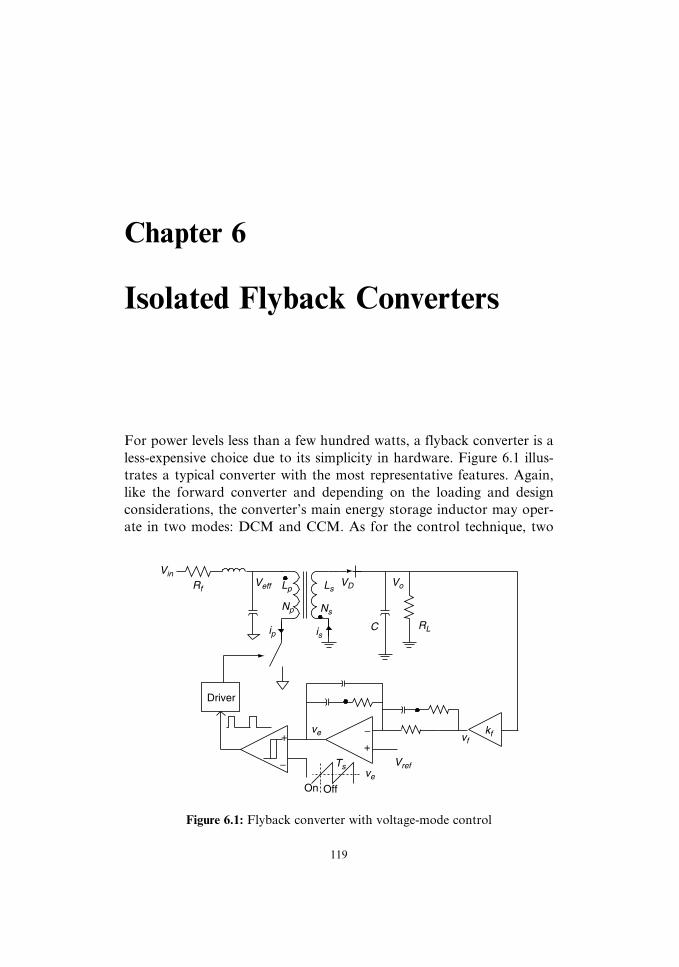
Chapter 6
Isolated Flyback Converters
For power levels less than a few hundred watts, a flyback converter is a
less-expensive choice due to its simplicity in hardware. Figure 6.1 illus-
trates a typical converter with the most representative features. Again,
like the forward converter and depending on the loading and design
considerations, the converter’s main energy storage inductor may oper-
ate in two modes: DCM and CCM. As for the control technique, two
119
Vo
Np Ns
Vin
isip
Veff VDRf
+
−+
− Ts
ve
Vref
Driver
vfkf
ve
On Off
Lp Ls
C RL
Figure 6.1: Flyback converter with voltage-mode control

approaches, voltage-mode control and current-mode control, are applic-
able. Wu [2] treated the subject in DCM using the voltage-mode and the
peak current-mode controls. We do not duplicate those efforts but
provide a refinement. We focus our coverage in the determination of
critical inductance, the AC small-signal studies for DCM with peak-
current mode, the DC studies for CCM with both voltage-mode and
current-mode, the steady-state time-domain output, and the like.
6.1 DCM Duty-Cycle Determination, AnotherApproach
In Wu [2], the DCM duty cycle was determined based on the concept of
total energy transfer. The book gives no information regarding the
duration of the conducting and nonconducting flyback phases, identified
as D2 and D3 in Figure 6.2, in which the relevant currents of a flyback
converter operating in DCM are given. We fill the gap here.
Based on simple geometry, the DC load current, Io, can be derived by
Io ¼Vo
RL
¼ 1
2. Isp
. D2 ¼1
2.Np
Ns
Ipp.D2 ¼
1
2.Np
Ns
.Veff . DDCM
Lp. fs
.D2 (6:1)
where Lp is the primary inductance and fs is the switching frequency.
However, (6.1) contains two unknowns, DDCM and D2. We need one
more equation. And it is provided by the volt–second balance across the
isolated inductor:
Veff . DDCM .Ts ¼Np
Ns
(Vo þ VD)D2 . Ts (6:2)
0
DCM
ipis
DDCMD2
IinIo
Ipp
D3
Isp
Figure 6.2: Currents for a flyback converter in DCM
120 CHAPTER 6. ISOLATED FLYBACK CONVERTERS

Both equations can be consolidated and solved for both unknowns. The
procedure leads to
D2DCM ¼
2 . Lp. fs . Vo
. (Vo þ VD)
V 2eff
. RL
(6:3)
Because of the input line resistance losses, the effective input is less
than the input:
Veff ¼ Vin � IinRf ¼ Vin �1
2Ipp
. DDCM ¼ Vin �1
2.Veff . DDCM
Lp. fs
. DDCM
Veff ¼2 . Lp
. fs . Vin
2 . Lp. fs þD2
DCM
(6:4)
In other words, (6.3) does not give the open-loop duty cycle yet. Equa-
tion (6.4) needs to be plugged into (6.3) to yield the end result:
D2DCM ¼
2 . Lp. fs . Vo
. (Vo þ VD)
2 . Lp. fs . Vin
2 .Lp. fs þD2
DCM
� �2
. RL
(6:5)
Evidently, it is not a trivial matter to find the DCM duty cycle in
symbolic closed form. We just leave it as it is with the understanding that
the open-loop output and the open-loop duty cycle for the converter are
now intimately related. In addition, it is interesting to interpret (6.5) in
another way. We note that the factor Vo(Vo þ VD)=RL actually repre-
sents the output power including rectifier losses. Therefore, (6.5) also ties
together the open-loop duty cycle and the output power.
6.2 CCM Duty-Cycle Determination
When CCM operation commences, the converter current waveforms
change shape, as shown in Figure 6.3, in which the following is estab-
lished:
6.2. CCM DUTY-CYCLE DETERMINATION 121

iA ¼Io
1�DCCM
þ (Vo þ VD)(1�DCCM)
2 . Ls. fs
iB ¼Io
1�DCCM
� (Vo þ VD)(1�DCCM)
2 . Ls. fs
Iin ¼Ns
Np
.DCCM
2(iA þ iB) ¼ Ns
Np
.DCCM
1�DCCM
. Io
(6:6)
Considering the input line resistance losses, the effective voltage
feeding the converter is reduced to
Veff ¼ Vin � Iin.Rf ¼ Vin �
Ns
Np
.DCCM
1�DCCM
.Vo
RL
. Rf (6:7)
Volt–second balance demands that
Veff . DCCM ¼Np
Ns
(Vo þ VD)(1�DCCM) (6:8)
Equation (6.7) is plugged into (6.8) to find the open-loop duty cycle:
Vin �Ns
Np
.DCCM
1�DCCM
.Vo
RL
.Rf
� �DCCM ¼
Np
Ns
(Vo þ VD)(1�DCCM)
(6:9)
Again, we do not attempt to solve the duty cycle in a symbolic,
explicit form. It is quite baffling if one compares (6.5) with (6.9). In the
0
0
ip
CCM
is
DCCM
1−DCCMIo
Ix2δi
iB
δiiA
Iin
Figure 6.3: Currents for a flyback converter in CCM
122 CHAPTER 6. ISOLATED FLYBACK CONVERTERS

case of DCM, more elements are involved, primary inductance and
switching frequency in particular. But there is no sign of involvement
for the two components in (6.9).
6.3 Critical Inductance
The critical inductance, which marks the transition boundary between
CCM and DCM, is obtained by setting iB ¼ 0:
iB ¼Io
1�DCCM
� (Vo þ VD)(1�DCCM)
2 . Ls. fs
¼ 0
Ls cri ¼(Vo þ VD)(1�DCCM)2
2 . Io . fs¼ (Vo þ VD)(1�DCCM)2
2 .Vo
RL
. fs
(6:10)
It is understood that DCCM in Ls cri is constrained by (6.9). Also, be
cautioned that (6.10) points to the critical inductance from the viewpoint
of the secondary side. The primary-side inductance is related to the
secondary-side inductance by turn ratio squared. Taking either side, we
are confronted by the utter complexity of such an outrageous equation
form. One may wonder if it can be reduced to a simpler form. Moreover,
(6.9) involves the turn ratio. We are still short one equation. The ad-
ditional constraint is given by the requirement that the switch voltage
rating must be larger than [(Vo þ VD)Np=Ns]þ Vin.
6.4 Voltage-Mode DCM Closed Loop
In Wu [2], this subject was briefly covered. Here, we give it better
coverage. Under closed-loop operation, the complete converter block
diagram can be as shown in Figure 6.4. Refer to Chapter 1 for the
derivation of the voltage loop error signal and PWM.
6.4. VOLTAGE-MODE DCM CLOSED LOOP 123

6.5 Voltage-Mode DCM Small-Signal Stability
In Chapter 2, a DCM canonical model, including a line input filter, was
developed. Figure 2.7 and equations (2.19) through (2.23) are universal
for all topologies. With a minor modification corresponding to Figure
6.1, we arrive at the AC block diagram in Figure 6.5 for the voltage-mode
in DCM. The block diagram simplifies to Figure 6.6 for the condition of
constant input. In the figures, EA(s) ¼ (1:45), Fm ¼ (1:46). However, we
should be careful to use the correct canonical parameters, j1, g1, r1, and
so forth in Gvd(s) for flyback converters.
Feedback
Power stage
Vin
PWM Error ampVe
Vo
DDCM
(1.28) (1.25)
(6.5)
Figure 6.4: Block diagram of a flyback converter DCM in closed-loop operation
vin
+ EA(s) Fm
H(s)
Ns /Np
++
d
(Ns /Np)2Zs
Gvd (s)
Gvg(s)
Kf
ve vo−
(2.22)
(2.23)
(1.46)ˆ
ˆ
Figure 6.5: AC block diagram for the voltage-mode in DCM; transfer functions
numbered have only the form, not the content, identified
124 CHAPTER 6. ISOLATED FLYBACK CONVERTERS

The loop gain is then simply
T(s) ¼ �Kf. EA(s) . Fm
. Gvd (s) (6:11)
and the conducted susceptibility is
Cs(s) ¼ H(s) .Ns
Np
. Gvg(s)1
1þ Kf. EA(s) . Fm . Gvd(s)
(6:12)
6.6 Voltage-Mode CCM Closed Loop
For CCM operation, the major change taking place is in the power stage
as outlined by (6.6) to (6.9). Other than that, there is no change in the
way the error amplifier and the PWM operate. We simply take Figure 6.4
and change the content for the power stage block. We obtain the steady-
state block diagram, Figure 6.7, for the subject.
+ EA(s) Fm
Kf
vo
− ve
Gvd (s)d
Figure 6.6: AC block diagram for the voltage-mode in DCM, constant input
Feedback
Power stage
Vin
PWM Error ampVe
Vo
DCCM
(1.28) (1.25)
(6.9)
Figure 6.7: Block diagram of a flyback converter CCM in closed-loop operation
6.6. VOLTAGE-MODE CCM CLOSED LOOP 125

6.7 Voltage-Mode CCM Small-Signal Stability
In Chapter 1, a CCM canonical model including line input filter was
developed. Figure 1.14 and equations (1.34) through (1.40) are universal
for all topologies. With a minor modification corresponding to Figure
6.1, we arrive at the AC block diagram, Figure 6.8, for voltage-mode in
CCM. Again, it reduces to Figure 6.9 for the condition with constant
input. It is a simple matter to write down the loop gain and the conducted
susceptibility given the two block diagrams. We just skip it.
6.8 Peak Current-Mode DCM Closed Loop
Current feedback is implemented by replacing the external oscillator in
Figure 6.1 with an embedded switch current that is properly isolated and
processed, as in Figure 6.10.
H(s)
Gvpg(s)
++Gvpd(s) He(s)
vp
vg
vse vd ˆ
ˆ
ˆ
ˆ
Vin
Fm
Kf
EA(s)veˆVref = 0
+−Ns
NpM
(1.46)
(1.39)
(1.40)
Figure 6.8: AC block diagram for the voltage-mode in CCM; transfer functions
numbered have only the form, not the content, identified
Gvpd (s) He(s)
vpˆ
vse vdFm
Kf
EA(s)veˆVref = 0 +− NpM
Ns
Figure 6.9: AC block diagram for the voltage-mode in CCM, constant input
126 CHAPTER 6. ISOLATED FLYBACK CONVERTERS
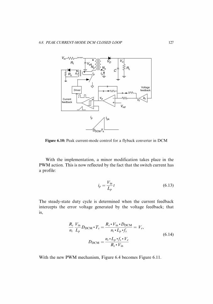
With the implementation, a minor modification takes place in the
PWM action. This is now reflected by the fact that the switch current has
a profile:
ip ¼Vin
Lp
t (6:13)
The steady-state duty cycle is determined when the current feedback
intercepts the error voltage generated by the voltage feedback; that
is,
Rs
ni
Vin
Lp
DDCM .Ts ¼Rs
. Vin. DDCM
ni.Lp
. fs¼ Ve,
DDCM ¼ni
. Lp. fs . Ve
Rs. Vin
(6:14)
With the new PWM mechanism, Figure 6.4 becomes Figure 6.11.
Vo
Np Ns
Vin
isip
VeffVDRf
+−+
−
ve
Vref
Driver
vfkfCurrent
feedback
Voltagefeedback
Rsni
CRL
Ipkip
DDCMTs
Figure 6.10: Peak current-mode control for a flyback converter in DCM
6.8. PEAK CURRENT-MODE DCM CLOSED LOOP 127
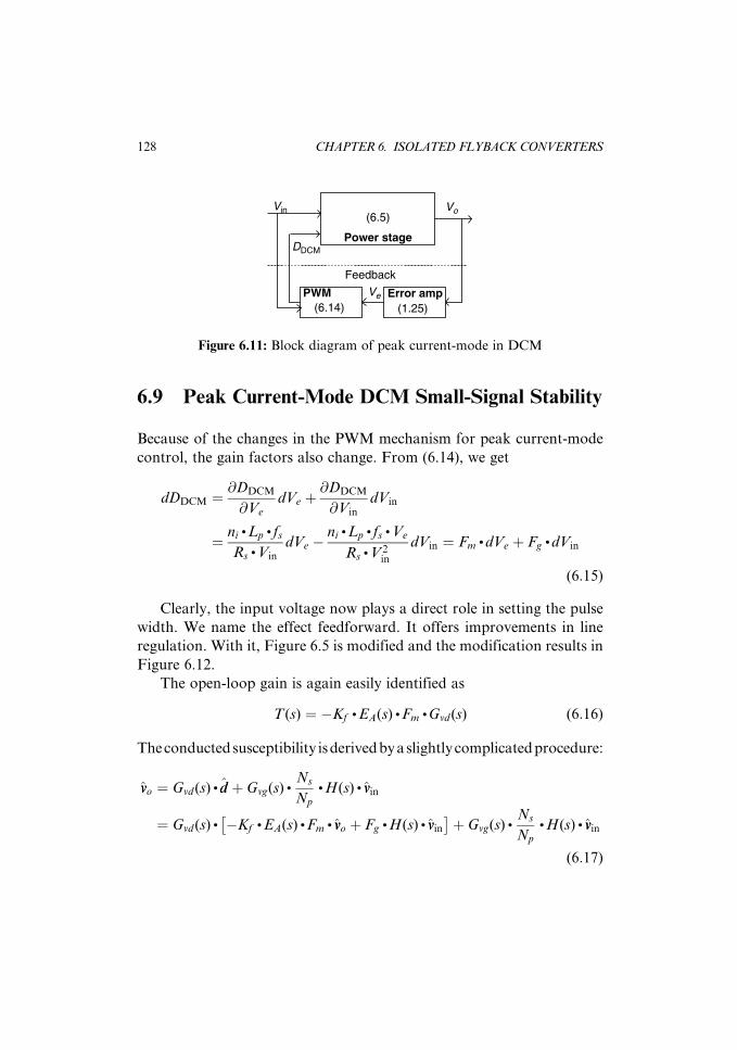
6.9 Peak Current-Mode DCM Small-Signal Stability
Because of the changes in the PWM mechanism for peak current-mode
control, the gain factors also change. From (6.14), we get
dDDCM ¼@DDCM
@Ve
dVe þ@DDCM
@Vin
dVin
¼ ni. Lp
. fs
Rs. Vin
dVe �ni
. Lp. fs . Ve
Rs. V 2
in
dVin ¼ Fm. dVe þ Fg
.dVin
(6:15)
Clearly, the input voltage now plays a direct role in setting the pulse
width. We name the effect feedforward. It offers improvements in line
regulation. With it, Figure 6.5 is modified and the modification results in
Figure 6.12.
The open-loop gain is again easily identified as
T(s) ¼ �Kf. EA(s) . Fm
.Gvd(s) (6:16)
Theconductedsusceptibility isderivedbyaslightlycomplicatedprocedure:
vvo ¼ Gvd(s) . dd þ Gvg(s) .Ns
Np
. H(s) . vvin
¼ Gvd(s) . �Kf. EA(s) . Fm
. vvo þ Fg.H(s) . vvin
� �þ Gvg(s) .
Ns
Np
. H(s) . vvin
(6:17)
Feedback
Power stage
Vin
PWM Error ampVe
Vo
DDCM
(6.14) (1.25)
(6.5)
Figure 6.11: Block diagram of peak current-mode in DCM
128 CHAPTER 6. ISOLATED FLYBACK CONVERTERS

Regrouping (6.17), we get conducted susceptibility:
Cs(s) ¼vvo
vvin
¼Fg
. Gvd(s)þ Gvg(s) .Ns
Np
� �.H(s)
1þ Kf. EA(s) . Fm
.Gvd(s)(6:18)
6.10 Peak Current-Mode CCM Closed Loop
Under a higher load or having a large energy storage inductor, the CCM
operation may commence. The switch current in this case changes shape
to what was shown in Figure 6.3. The steady-state block diagram is
changed accordingly. First, the analytical form for the switch current
needs to be modified:
ip ¼Ns
. iB
Np
þ Vin
Lp
t (6:19)
+ EA(s)+
+Fm
H(s)
Ns /Np
++
d+
vin
Fg
Gvd (s)
Gvg(s)
Kf
ve
vo−
(6.15)
ˆ
ˆ
ˆ
Figure 6.12: AC block diagram for peak current-mode in DCM
6.10. PEAK CURRENT-MODE CCM CLOSED LOOP 129

where iB is from (6.6). By the same logic mentioned in Section 6.8, the
steady-state duty cycle under CCM operation is derived:
Ns. iA . Rs
Np.ni
¼Ns. Rs
Np.ni
Vo
(1�DCCM)RL
þ (VoþVD)(1�DCCM)
2 . Ls. fs
� �¼Ve (6:20)
We can also rewrite (6.20):
Ns. Rs
Np.ni
Vo. Np
. (Vo þ VD)
RL. Ns
. Vin. DCCM
þNs. Vin
.DCCM
2 . Ls. fs . Np
� �¼ Ve (6:21)
However, unlike (6.14), DCCM cannot be neatly expressed as an explicit
function of other circuit components and parameters. We do not attempt
to solve it. But we still have a block diagram for this subject in the steady
state (Figure 6.13).
We notice that one more interesting effect is added: The PWM action
is also under the direct influence of the output. Is there some advantage,
or disadvantage, in terms of performance? It is not clear.
6.11 Peak Current-Mode CCM Small-SignalStability
By the same argument stated in section 6.9 and the fact of (6.21), the
PWM gain factors for this section are much more sophisticated. Explicit,
Power stage
Vin
PWM Error ampVe
Vo
DCCM
(6.21) (1.25)
(6.9)
Figure 6.13: Block diagram of peak current-mode in CCM
130 CHAPTER 6. ISOLATED FLYBACK CONVERTERS

symbolic derivatives are out of the question. We again resort to the
implicit function approach. We first define
f (Ve, Vin, Vo, DCCM, : : :)
¼ Ns. Rs
Np. ni
.Vo
. Np. (Vo þ VD)
RL. Ns
. Vin. DCCM
þNs. Vin
.DCCM
2 . Ls. fs . Np
� �� Ve ¼ 0 (6:22)
We then derive all three modulation gains by
dDDCM ¼ Fm.dVe þ Fg
. dVin þ Fv. dVo
¼ � (@f =@Ve)
(@f =@DCCM)dVe �
(@f =@Vin)
(@f =@DCCM)dVin �
(@f =@Vo)
(@f =@DCCM)dVo
(6:23)
Subsequently, the overall block diagram (Figure 6.14) is given.
The loop gain under the condition of constant input is
T(s) ¼ �Kf. EA(s) . Fm
.
Gvpd(s) .Ns
Np. M0
.He(s)
1þ Fv.Gvpd(s) .
Ns
Np. M0
. He(s)
(6:24)
H(s)
Gvpg(s)
++ Ns /(NpM )Gvpd(s) He(s)vpˆ
vgˆ
vseˆ v
vinˆ
Kf
EA(s)veˆVref =0
+−+++Fm
Fv
Fg
dD
Figure 6.14: AC block diagram for peak current-mode in CCM
6.11. PEAK CURRENT-MODE CCM SMALL-SIGNAL STABILITY 131

where EA(s) is not signed. And the conducted susceptibility is
Cs(s) ¼H(s) . [Gvpd(s) .Fg þ Gvpg(s)]
Ns
Np. M0
. He(s)
1þ [Kf. EA(s) . Fm � Fv] .Gvpd(s) .
Ns
Np. M0
. He(s)
(6:25)
6.12 Output Capacitor
Referring to Figure 6.1 or Figure 6.10, we here find the proper size for
the output capacitor such that it meets the output ripple voltage require-
ment, dv. We first find the one for DCM, then that for CCM.
Under the DCM, and if we ignore the input filter losses Rf , the
secondary current is given by (referring to Figure 6.2):
is(t) ¼ Isp �Vo þ VD
Ls
t ¼ Np
Ns
ffiffiffiffiffiffiffiffiffiffiffiffiffiffiffiffiffiffiffiffiffiffiffiffiffiffiffiffiffiffiffiffiffiffiffi2 .Vo
. (Vo þ VD)
Lp. fs . RL
s� Vo þ VD
Ls
t (6:26)
Since thecapacitordoesnotpassDCcurrent, theACcurrent is thengivenas
ic(t) ¼ is(t)�Vo
RL
¼ Np
Ns
ffiffiffiffiffiffiffiffiffiffiffiffiffiffiffiffiffiffiffiffiffiffiffiffiffiffiffiffiffiffiffiffiffiffiffi2 . Vo
. (Vo þ VD)
Lp. fs . RL
s� Vo þ VD
Ls
t� Vo
RL
(6:27)
We are used to the differential equation C . dv=dt ¼ ic for capacitor
current. We also understand from calculus that, if the behavior of a
variable x is governed by a simple differential equation, a . dx=dt ¼ b,
the variable’s extreme (maximum or minimum) value occurs at b ¼ 0. By
the same token, we say the output capacitor voltage peaks at zero current
crossing. We next find the current zero-crossing time, t0:
ic(t0) ¼Np
Ns
ffiffiffiffiffiffiffiffiffiffiffiffiffiffiffiffiffiffiffiffiffiffiffiffiffiffiffiffiffiffiffiffiffiffiffi2 .Vo
. (Vo þ VD)
Lp. fs . RL
s� Vo þ VD
Ls
t0 �Vo
RL
¼ 0
t0 ¼
Np
Ns
ffiffiffiffiffiffiffiffiffiffiffiffiffiffiffiffiffiffiffiffiffiffiffiffiffiffiffiffiffiffiffiffiffiffiffi2 .Vo
. (Vo þ VD)
Lp. fs . RL
s� Vo
RL
Vo þ VD
Ls
(6:28)
132 CHAPTER 6. ISOLATED FLYBACK CONVERTERS
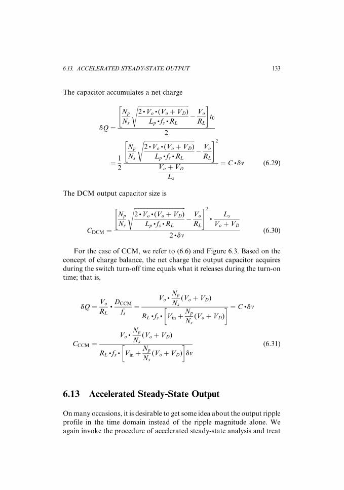
The capacitor accumulates a net charge
dQ ¼
Np
Ns
ffiffiffiffiffiffiffiffiffiffiffiffiffiffiffiffiffiffiffiffiffiffiffiffiffiffiffiffiffiffiffiffiffiffiffi2 . Vo
. (Vo þ VD)
Lp. fs .RL
s� Vo
RL
" #t0
2
¼ 1
2
Np
Ns
ffiffiffiffiffiffiffiffiffiffiffiffiffiffiffiffiffiffiffiffiffiffiffiffiffiffiffiffiffiffiffiffiffiffiffi2 .Vo
. (Vo þ VD)
Lp. fs . RL
s� Vo
RL
" #2
Vo þ VD
Ls
¼ C . dv (6:29)
The DCM output capacitor size is
CDCM ¼
Np
Ns
ffiffiffiffiffiffiffiffiffiffiffiffiffiffiffiffiffiffiffiffiffiffiffiffiffiffiffiffiffiffiffiffiffiffiffi2 . Vo
. (Vo þ VD)
Lp. fs .RL
s� Vo
RL
" #2
.Ls
Vo þ VD
2 . dv(6:30)
For the case of CCM, we refer to (6.6) and Figure 6.3. Based on the
concept of charge balance, the net charge the output capacitor acquires
during the switch turn-off time equals what it releases during the turn-on
time; that is,
dQ ¼ Vo
RL
.DCCM
fs¼
Vo.Np
Ns
(Vo þ VD)
RL. fs . Vin þ
Np
Ns
(Vo þ VD)
� � ¼ C . dv
CCCM ¼Vo
.Np
Ns
(Vo þ VD)
RL. fs . Vin þ
Np
Ns
(Vo þ VD)
� �dv
(6:31)
6.13 Accelerated Steady-State Output
On many occasions, it is desirable to get some idea about the output ripple
profile in the time domain instead of the ripple magnitude alone. We
again invoke the procedure of accelerated steady-state analysis and treat
6.13. ACCELERATED STEADY-STATE OUTPUT 133
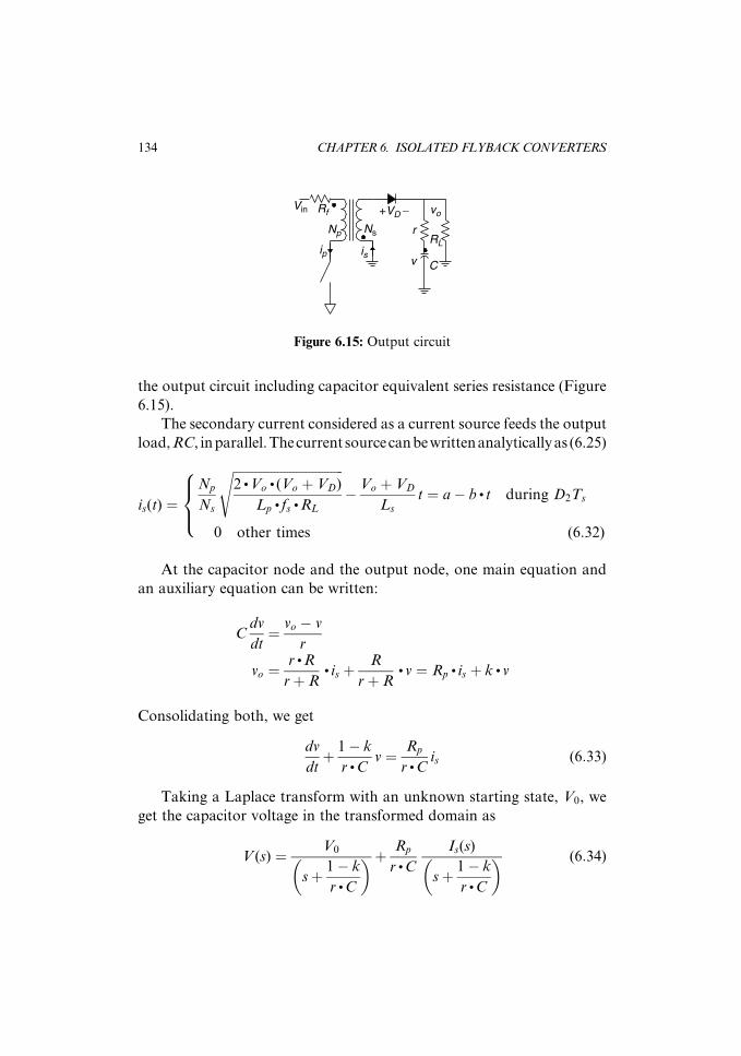
the output circuit including capacitor equivalent series resistance (Figure
6.15).
The secondary current considered as a current source feeds the output
load,RC, inparallel.Thecurrent sourcecanbewrittenanalyticallyas (6.25)
is(t) ¼Np
Ns
ffiffiffiffiffiffiffiffiffiffiffiffiffiffiffiffiffiffiffiffiffiffiffiffiffiffiffiffiffiffiffiffiffiffiffi2 . Vo
. (Vo þ VD)
Lp. fs . RL
s� Vo þ VD
Ls
t ¼ a� b . t during D2Ts
0 other times (6:32)
8><>:
At the capacitor node and the output node, one main equation and
an auxiliary equation can be written:
Cdv
dt¼ vo � v
r
vo ¼r . R
rþ R. is þ
R
rþ R. v ¼ Rp
. is þ k . v
Consolidating both, we get
dv
dtþ 1� k
r . Cv ¼ Rp
r . Cis (6:33)
Taking a Laplace transform with an unknown starting state, V0, we
get the capacitor voltage in the transformed domain as
V (s) ¼ V0
sþ 1� k
r . C
� �þ Rp
r .C
Is(s)
sþ 1� k
r .C
� � (6:34)
RL
vo
Np Ns
Vin
isip
r
v
Rf +VD −
C
Figure 6.15: Output circuit
134 CHAPTER 6. ISOLATED FLYBACK CONVERTERS

where
Is(s) ¼a
s� b
s20 < t < D2 . Ts
0 D2 . Ts < t < Ts
8<: (6:35)
As a result, we have, for the two time segments,
V2(s) ¼V02
sþ 1� k
r . C
� �þ Rp
r . C
a
s sþ 1� k
r . C
� �� Rp
r . C
b
s2 sþ 1� k
r . C
� �
V1(s) ¼V01
sþ 1� k
r . C
� � e�D2. Ts
. s (6:36)
Inverse Laplace transformation gives us the ideal capacitor voltage:
v2(t) ¼ V02 . f1(t)þRp
.a
r . C. f2(t)�
Rp.b
r . C. f3(t)
� �[u(t)� u(t�D2Ts)]
v1(t) ¼ [V01 . f1(t�D2 .Ts)][u(t�D2Ts)� u(t� Ts)] (6:37)
Continuity of states at the two time boundaries, D2Ts and Ts, yields
V01�V02 . f1(D2 . Ts)¼Rp
. a
r .C. f2(D2 .Ts)�
Rp. b
r . C. f3(D2 . Ts)
V01 . f1(Ts�D2 . Ts)�V02¼ 0
(6:38)
Equation (6.38) enables us to solve the two unknown, cyclic starting
states, V01 and V02. With this knowledge, the main output is given:
vo(t) ¼Rp
Np
Ns
.Vin
. DDCM
Lp. fs
� Vo þ VD
Ls
t
� �[u(t)� u(t�D2Ts)]þ k . v2(t)
k . v1(t) (6:39)
8><>:
Both equations (6.37) and (6.39) and the estimate of equivalent series
resistance, r, also give us the ripple current, and consequently power
dissipation, for the capacitor:
6.13. ACCELERATED STEADY-STATE OUTPUT 135
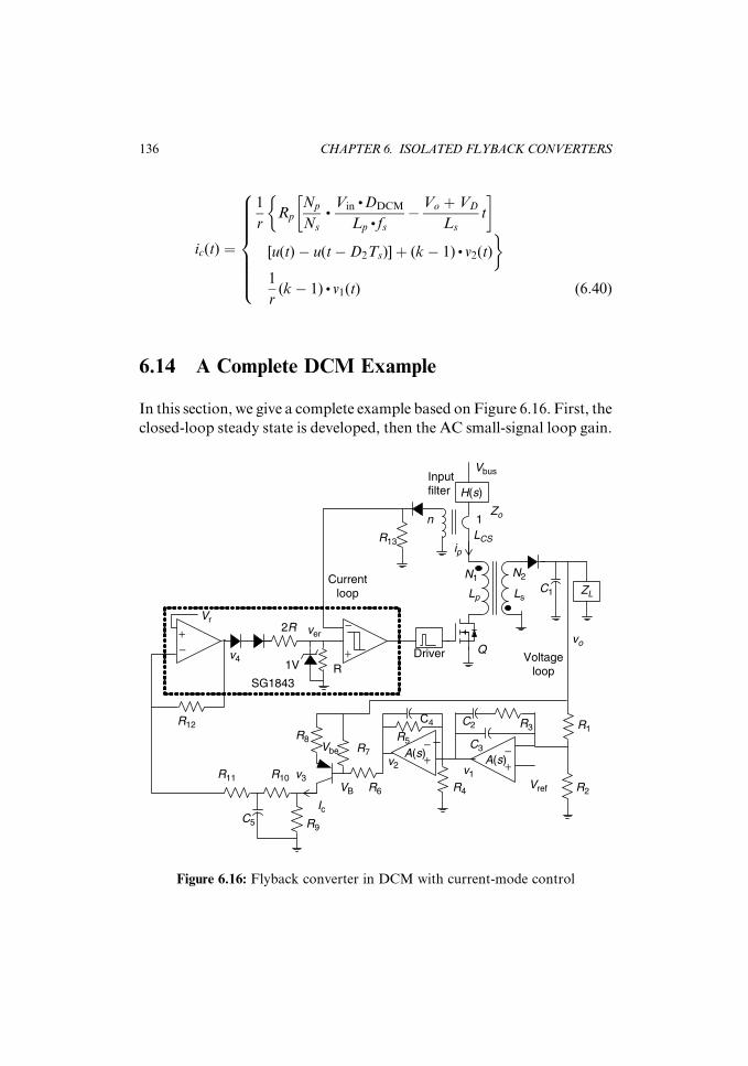
ic(t) ¼
1
rRp
Np
Ns
.Vin
. DDCM
Lp. fs
� Vo þ VD
Ls
t
� ��
[u(t)� u(t�D2Ts)]þ (k� 1) . v2(t)
1
r(k� 1) . v1(t)
8>>>>>><>>>>>>: (6:40)
6.14 A Complete DCM Example
In this section, we give a complete example based on Figure 6.16. First, the
closed-loop steady state is developed, then the AC small-signal loop gain.
ip
N1 N2C1Lp Ls
ZL
+−
+−
+
−+−
Vref
VbusInputfilter H(s)
LCS
n 1Zo
Vr2R
R
R1
R2
R3
R4
R5
R6
R7
R8
R9
R10R11
R12 C2
C3
C4
vo
v4
v3
v2 v1
Vbe A(s) A(s)
Voltageloop
Currentloop
SG1843
Driver1V
ver
VB
Ic
R13
C5
Q
Figure 6.16: Flyback converter in DCM with current-mode control
136 CHAPTER 6. ISOLATED FLYBACK CONVERTERS
A. Steady-State Closed-Form Output Equation
The operation of the converter can be briefly described as follows. At the
initiation of an internal clock, fs, residing in the PWM integrated circuit,
SG1843 (silicon general semiconductor), the power switch, Q, is turned
on. This action generates a ramping up current, ip, at the primary
winding with a slope determined by the associated primary inductance,
Lp, and the effective input voltage, Vb. Meanwhile, the output voltage, vo,
is processed by the feedback loop and eventually transformed into a
control (error) voltage, ver. Both the control voltage and the scaled
version of the ramp current are fed to a hysteretic comparator. At the
instant the sensed current in voltage form intercepts the control voltage,
the power switch ceases conduction and remains off until the next clock-
on cycle.
At the steady state, that is, under a constant load and constant line
input, the intermediate control voltage v2 is expressed as
v2 ¼M1 �M2 . vo (6:41)
where
M1 ¼ 1þ R5
R4
� �A . Vref
M2 ¼ 1þ R5
R4
� �A .
R2
R1 þ R2
Subsequent stages of transconductance amplifier and operational
amplifier develop the intermediate control voltage further and generate
Ic ¼M3 . v2 þM4 . vo þM5
v3 ¼M6 þM7 . Ic
ver ¼M8 þM9 . v3
(6:42)
6.14. A COMPLETE DCM EXAMPLE 137

where
M3 ¼ hFE
R7
�[R7 .R6 þ (1þ hFE)R8(R7 þ R6)]
M4 ¼ �M3
M5 ¼ hFE
(R7 þ R6)Vbe
�[R7 .R6 þ (1þ hFE)R8(R7 þ R6)]
M6 ¼R9
R9 þ R10 þ R11
Vr
M7 ¼R9(R11 þ R10)
R9 þ R10 þ R11
M8 ¼1
31þ R12
R11 þ R10
� �Vr � 2 . VD
� �
M9 ¼1
3.
R12
R11 þ R10
The effective error voltage, ver, in turn, generates a steady-state duty
cycle:
D ¼ n . Lp. fs
Vb. R13
. ver ¼M10 . ver (6:43)
and the output
vo ¼ D .Ns
.Vbus
Np
ffiffiffiffiffiffiffiffiffiffiffiffiffiffiffiffiffiRL
2 . Ls. fs
s¼ D . M11 (6:44)
where the power stage gain, M11, is given in section 6.1 in approximation.
The preceding set of equations can then be back substituted starting from
(6.44) using all M, and the process yields the closed-form, closed-loop
output:
vo ¼M10 . M11 . {M8 þM9[M6 þM7(M3 . M1 þM5)]}
1þM10 . M11 .M9 . M7(M3 .M2 �M4)(6:45)
138 CHAPTER 6. ISOLATED FLYBACK CONVERTERS

B. Output Sensitivity
The closed-form solution gives designers the ability to evaluate many
performance merits of a design analytically and numerically. Among
them, load regulation, line regulation, and component sensitivities are
the three most sought after figures. For instance, the load regulation
sensitivity can be expressed as
SR ¼@vo
@M11
@M11
@RL
(6:46)
C. AC Loop Gain
To study the small-signal behavior of the converter, the schematic of
Figure 6.16 is transformed into Figure 6.17, in which the transfer func-
tions of individual blocks are identified and derived as follows.
Figure 6.18(b) gives the corresponding small-signal equivalent circuit
of the first stage of error amplifier. Based on the equivalent circuit and
considering the nonideal gain, A(s), of the operational amplifier, the
input-to-output transfer function is obtained:
EA1(s) ¼v1
vo
¼ � R2
R1 þ R2
.A(s)
Rp
1
Rp
þ 1þ A(s)
Zf 1(s)
� � (6:47)
++ EA1(s) EA2(s) Gt 2(s)
++ Ae(s)
Gt 1(s)
Fm Gvd (s)
v1 v2 v3 ver d vo
SG1843
Figure 6.17: Small-signal block diagram (constant input form)
6.14. A COMPLETE DCM EXAMPLE 139

+−
Vref
R1
R2
R3C2
C3
v1
A(s)
vo
+−
Rp = R1//R2R3C2
C3
v1
A(s)vokfvo
R1+R2
R2 ⋅=
Zf 1
(a) (b)
Figure 6.18: Error amplifier: (a) DC, (b) AC AQ1
where Rp ¼ R1=R2 and
A(s) ¼ A
s
2 . p . fpþ 1
� �
represents the open-loop gain of the operational amplifier with single-
pole gain-roll-off at frequency fp and DC gain A, which is also used in M1
and M2.
By exactly the same procedure, the second-stage error amplifier gives
EA2(s) ¼v2
v1
¼ A(s) 1� A(s)
Zf 2(s) .1þ A(s)
Zf 2(s)þ 1
R4
� �8>><>>:
9>>=>>; (6:48)
For the transistor voltage-to-current converter, more steps are in-
volved. Figure 6.19 gives both the DC and AC circuits of the circuit.
Three nodal equations can be written for Figure 6.19(b):
1
R6
þ 1
R7
þ 1
hi
� �vB �
1
hi
vx ¼vo
R7
þ v2
R6
1þ hf
hi
vB �1
R8
þ 1þ hf
hi
� �vx ¼ �
vo
R8
hf
hi
vB �hf
hi
vx þ1
Zc(s)vc ¼ 0
(6:49)
140 CHAPTER 6. ISOLATED FLYBACK CONVERTERS

R7
R8
R9
R10R11v3
Vbe
VB
C5
R6
v2
vo
Zc
R7
R8
VB R6
vo
Zc
v2
hie
vx
hFEib
ib
vc
(a) (b)
Figure 6.19: Transistor buffer: (a) DC, (b) AC
The equation set yields, at note vc,
vc ¼
1
R6
þ 1
R7
þ 1
hi
� 1
hi
vo
R7
þ v2
R6
1þ hf
hi
� 1
R8
þ 1þ hf
hi
� �� vo
R8
hf
hi
� hf
hi
0
De
(6:50)
and the transistor stage gains
Gt1(s) ¼@vc
@vo
¼
1þ hf
hi
� 1
R8
þ 1þ ht
ht
� �hf
hi
� hf
hi
1
R7
þ
1
R6
þ 1
R7
þ 1
h1
�11
hi
hf
hi
� hf
hi
1
R8
De
(6:51)
Gt2(s) ¼@vc
@v2
¼
1þ hf
hi
� 1
R8
þ 1þ hf
hi
� �hf
hi
� hf
hi
1
R6
De
6.14. A COMPLETE DCM EXAMPLE 141

where
De ¼
1
R6
þ 1
R7
þ 1
hi
�1
hi
0
1þ hf
hi
� 1
R8
þ 1þ hf
hi
� �0
hf
hi
�hf
hi
1
Zc(s)
Following the voltage-to-current converter, the internal error ampli-
fier of the PWM IC yields one more transfer function, based on Figure
6.20; that is,
Ae(s) ¼ver
v3
¼ ver
veq
veq
v3
¼ � 1
3.
R12
R11 þ1
R10
þ C5 . s
� ��1.
(C5 . s)�1
R10 þ (C5 . s)�1(6:52)
With both the effective error voltage and the current feedback avail-
able at the input terminals of the comparator, the steady-state duty cycle
is established, given by (6.43). The AC, small-signal perturbation of
(6.43) produces
dD ¼ Fm. dver þ Fg
. dVbus (6:53)
+−
Vr2R
R
R12
v4 1 V
ver
SG1843
R10
R11
v3
C5
+−
R12
v4
SG1843
R10
R11
v3
C5
1/3 ver
veq
(a) (b)
Figure 6.20: PWM internal error amplifier: (a) DC, (b) AC
142 CHAPTER 6. ISOLATED FLYBACK CONVERTERS
where
Fm ¼@D
@ver
¼ Lp. fs . n
Rs.Vbus
, Fg ¼@D
@Vbus
¼ �Lp. fs .n .Ver
Rs. V 2
bus
The last, but not the least important, block that needs to be devel-
oped is the power stage. The development of power stage transfer func-
tion is accomplished by invoking the canonical model and modifying it
such that the magnetic isolation and the line input filter are included and
reflected to the secondary side as given in (2.22) section 2.2. The power
stage duty cycle-to-output transfer function can be shown to be (Zo, the
output impedance of input filter, g1 ¼ 0)
Gvd(s) ¼ 1� g2
j1
j2
r1 . Zs(s)
r1 þ Zs(s)
� �j2
1
ZL(s)þ 1
r2
þ C1 . s
(6:54)
where
Zs(s) ¼N2
N1
� �2
Zo(s)
Once all blocks have been treated for AC analysis, the base diagram
of Figure 6.17 can be further simplified to result in Figure 6.21. This step
is taken because a loop-gain study must be conducted under a steady
state, that is, with a constant input and constant load. It is also pointed
out that, due to the transistor voltage-to-current converter, multiple
loops exist. However, the outer loop is considered the main loop, since
this is where the command reference is applied. With this selection of
++ EA1(s) EA2(s) Gt 2(s)
v1 v2 vo
1−Gt 1(s) ⋅ Ae(s) ⋅ Fm ⋅ Gvd(s)
Ae(s) ⋅ Fm ⋅ Gvd(s)
Figure 6.21: Block diagram for loop gain
6.14. A COMPLETE DCM EXAMPLE 143

loop definition and by absorbing the inner loop as shown in Figure 6.21,
the loop gain is finally given as
T(s) ¼ EA1(s) . EA2 . Gt2(s) .Ae(s) . Fm. Gvd(s)
1� Gt1(s) .Ae(s) . Fm. Gvd (s)
(6:55)
To verify the validity of the loop-gain formulation process, the end
result (6.55) is computed for an actual design. The theoretical results,
shown in Figure 6.22, compare extremely well against the actual mea-
surement of Figure 6.23. The comparison hence gives credence to (6.55).
−30
−20
−10
0
10
20
30
40
50
60
7070
−30
−100
200
TdB(n)
0
1 ⋅ 1051 ⋅ 1041 ⋅ 10310010−180
−135
−90
−45
0
45
90
135
180180
−180
α(n)
0
100 ⋅ Kf(n)10
1 ⋅ 1051 ⋅ 1041 ⋅ 10310010
100 ⋅ Kf(n)10
Figure 6.22: Theoretical loop gain: Gain 10dB/div; Phase 458/div
144 CHAPTER 6. ISOLATED FLYBACK CONVERTERS

D. Conducted Susceptibility
Conducted susceptibility is a measure of how well the converter rejects
input perturbation dVbus. This performance parameter is made particu-
larly necessary for specifying supplies powering RF equipment, since
poor supply rejection exhibited by the equipment can cause contamin-
ation of RF transmissions. It is therefore very desirable to estimate in
advance the parameter figure for a converter. This task can be performed
by reconfiguring and modifying Figure 6.17, which results in Figure 6.24.
Here, caution should be exercised in formulating the control loop-gain,
because two feedback paths coexist. Moreover, a slight complication also
exists in the input chain; that is, the presence of feedforward effect, Fg,
which plays a part in perturbing the duty cycle, too. However, as shown
in (6.15), the feedforward coefficient is inversely proportional to the
square of the input, Vbus. Its magnitude is, in effect, much smaller than
Magnitude
Phase
0
10 100 1k 10k 100k
Figure 6.23: Actual measurement: Magnitude 10dB/div; Phase 458/div
6.14. A COMPLETE DCM EXAMPLE 145

the feedback coefficient, Fm, which is inversely proportional to Vbus. The
feedforward effect can be included and lead to a reformulated loop-gain
equation:
TCS(s) ¼ [EA1(s) . EA2(s) . Gt2(s)þ Gt1(s)] . Ae(s) . Fm. Gvd(s) (6:56)
EA1(s) EA2(s) Gt2(s)+
+ Ae(s)
Gt1(s)
FmPowerstage
H(s)
v1 v2 v3 ver d vo
Zs
++
Fg
δVbus
Figure 6.24: Block diagram for conducted susceptibility
100 1⋅1031⋅104 1⋅105
−100
−90
−80
−70
−60
−50
−40
−30
−20
−10
00
−100
100 ⋅ K100 f(n)
CS
dB(n
)
Figure 6.25: Conducted susceptibility, theoretical: 10dB/div
146 CHAPTER 6. ISOLATED FLYBACK CONVERTERS

The resultant conducted susceptibility is then expressed as
CS(s) ¼
N2
N1
H(s)r1
Zs(s)þ r1
g2
1
ZL(s)þ 1
r2
þ C1 . s
þ Fg. Gvd(s)
2664
3775
1� TCS(s)(6:57)
Again, the analytical computation of (6.57) yields Figure 6.25, which
also matches the actual measurement, Figure 6.26, extremely well.
0
100 1K Frequency 10K 100K
Figure 6.26: Conducted susceptibility, measurement; �10dB=div
6.14. A COMPLETE DCM EXAMPLE 147

This page intentionally left blank

Chapter 7
Nonisolated Boost Converter
We shall depart from the presentation flow that has been the hallmark
for the past six. Since current-mode control enjoys obvious advantages
over voltage-mode control, we can omit the latter without disrupting the
key aspects of the chapter. Because of that, this will be a short chapter.
Nevertheless, we cover duty-cycle determination, critical inductance, and
the steady state under closed loop, loop gain, and the like. All analyses
focus on a single schematic, Figure 7.1, which is derived from Figure 6.10
by replacing the power stage with the nonisolated boost stage.
7.1 Duty-Cycle Determination
Figure 7.1 also shows major current waveforms for DCM and CCM
operations. Given that, the procedure for determining the duty cycle for
both cases is basically the same as that for the flyback converters. The
case for CCM was covered in Wu [2]. We consider only DCM in this
section.
We start with the requirement of volt–second, flux balance across the
boost inductor L:
Veff . DDCM þ [Veff � (VD þ Vo)] .D2 ¼ 0 (7:1)
149

The switch peak current is
Ipk ¼Veff
L . fs.DDCM (7:2)
The input line has a DC current
Iin ¼1
2(DDCM þD2)Ipk ¼
1
2(DDCM þD2)
Veff
L . fs. DDCM (7:3)
Considering the input losses Rf , the effective input is
Vin
iqid Vo
Veff VDRf
+
−+
−
ve
Vref
Driver
kfvfCurrent
feedback
Voltagefeedback
Rs RLni
C
LiL
iL iL
id
Io
id iAiB
iq iq
Ipk
Ipk
Ipk
DDCMTs DCCMTs
0
0
0
D2Ts
Ts Ts
DCM
0
0
0
(1 − DCCM)Ts
CCM
Figure 7.1: Nonisolated boost converter
150 CHAPTER 7. NONISOLATED BOOST CONVERTER
Veff ¼ Vin � IinRf ¼ Vin �1
2DDCM þ
Veff . DDCM
Vo þ VD � Veff
� �Veff
L . fs.DDCM . Rf
Veff ¼ Vin �1
21þ Veff
Vo þ VD � Veff
� �Veff
L . fs. D2
DCM. Rf (7:4)
The DC load current is given as
Vo
RL
¼ 1
2D2 . Ipk ¼
V 2eff
.D2DCM
2 .L . fs(Vo þ VD � Veff )(7:5)
The open-loop DCM duty cycle is embedded in (7.4) and (7.5).
7.2 Critical Inductance
From the CCM current waveform, we again understand that the critical
inductance can be decided by the boundary condition iB ¼ 0:
iB ¼Io
1�DDCM
� (Vo þ VD � Vin) . (1�DCCM)
2 . Lcri. fs
¼ 0
Lcri ¼(Vo þ VD � Vin)V
2in
2 . Io. fs . (Vo þ VD)2
(7:6)
7.3 Peak Current-Mode Closed-Loop Steady Statein CCM
Based on the current waveform given in Figure 7.1, the main power
switch terminates conduction when the current feedback signal in voltage
form crosses the control error voltage generated by the voltage feedback
loop; that is,
Ve ¼Rs
ni
iA ¼Rs
ni
Vo
(1�DCCM)RL
þ Vin. DCCM
2 . L . fs
� �(7:7)
7.2. CRITICAL INDUCTANCE 151

With (7.7) available, we are ready to close the loop. This leads to
Figure 7.2.
If so desired, readers can replace the approximation for the power
stage with the more accurate one that accounts for losses and was given
in Wu [2].
7.4 Peak Current-Mode Small-Signal Stabilityin CCM
Following the same steps for other converters, we derive the small-signal
gains for the PWM block by defining an implicit function:
f (Ve, Vo, Vin, DCCM) ¼ Ve �Rs
ni
Vo
(1�DCCM)RL
þ Vin.DCCM
2 . L . fs
� �¼ 0
(7:8)
The small-signal gains are then
dDCCM ¼ Fm. dVe þ Fv
. dVo þ Fg. dVin
¼ � @f =@Ve
@f =@DCCM
dVe �@f =@Vo
@f =@DCCM
dVo �@f =@Vin
@f =@DCCM
dVin
(7:9)
This is shown in Figure 7.3.
Feedback
Power stage
Vin
PWM Error amp
Ve
Vo
DCCM
(1.25)(7.7)
−VD = Vo
Vin
1− DCCM
Figure 7.2: Nonisolated boost converter in the steady state, CCM
152 CHAPTER 7. NONISOLATED BOOST CONVERTER
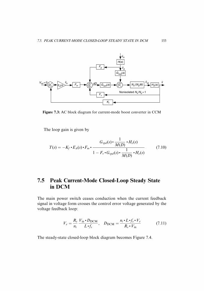
The loop gain is given by
T(s) ¼ �Kf.EA(s) .Fm
.
Gvpd(s) .1
M(D). He(s)
1� Fv. Gvpd(s) .
1
M(D). He(s)
(7:10)
7.5 Peak Current-Mode Closed-Loop Steady Statein DCM
The main power switch ceases conduction when the current feedback
signal in voltage form crosses the control error voltage generated by the
voltage feedback loop:
Ve ¼Rs
ni
Vin.DDCM
L . fs, DDCM ¼
ni. L . fs .Ve
Rs. Vin
(7:11)
The steady-state closed-loop block diagram becomes Figure 7.4.
H(s)
Gvpg(s)
++ Ns
/(NpM)Gvpd(s) He(s)
vin
vse v
vg
Kf
Fv
Fg
FmEA(s)veVref = 0
+−++
+ dD
Nonisolated Ns/Np = 1
Figure 7.3: AC block diagram for current-mode boost converter in CCM
7.5. PEAK CURRENT-MODE CLOSED-LOOP STEADY STATE IN DCM 153
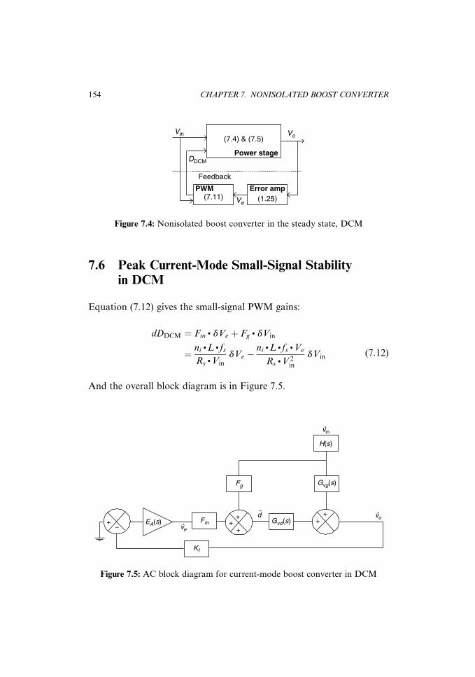
7.6 Peak Current-Mode Small-Signal Stabilityin DCM
Equation (7.12) gives the small-signal PWM gains:
dDDCM ¼ Fm. dVe þ Fg
. dVin
¼ ni.L . fs
Rs. Vin
dVe �ni
. L . fs . Ve
Rs. V 2
in
dVin (7:12)
And the overall block diagram is in Figure 7.5.
Feedback
Power stage
Vin
PWM Error amp
Ve
Vo
DDCM
(1.25)(7.11)
(7.4) & (7.5)
Figure 7.4: Nonisolated boost converter in the steady state, DCM
+ EA(s)+
+
H(s)
++
d+
vin
vo
Fg
Fm
Kf
Gvd(s)
Gvg(s)
ve−
Figure 7.5: AC block diagram for current-mode boost converter in DCM
154 CHAPTER 7. NONISOLATED BOOST CONVERTER

The control loop gain is
T(s) ¼ �Kf. EA(s) . Fm
. Gvd (s) (7:13)
7.7 DCM Output Capacitor Size
For DCM, the pulsating output current, id , is given as
id(t) ¼ Ipk �Vo þ VD � Vin
Lt ¼ Veff . DDCM
L . fs� Vo þ VD � Vin
Lt (7:14)
For engineering purposes, the line input series loss can be ignored. In that
case, (7.14) becomes
id(t) ¼
ffiffiffiffiffiffiffiffiffiffiffiffiffiffiffiffiffiffiffiffiffiffiffiffiffiffiffiffiffiffiffiffiffiffiffiffiffiffiffiffiffi2(Vo þ VD � Vin)Vo
L . fs . RL
s� Vo þ VD � Vin
Lt (7:15)
The output capacitor current is then given as
ic(t) ¼
ffiffiffiffiffiffiffiffiffiffiffiffiffiffiffiffiffiffiffiffiffiffiffiffiffiffiffiffiffiffiffiffiffiffiffiffiffiffiffiffiffi2(Vo þ VD � Vin)Vo
L . fs . RL
s� Vo
RL
� Vo þ VD � Vin
Lt (7:16)
It crosses zero at
t0 ¼
ffiffiffiffiffiffiffiffiffiffiffiffiffiffiffiffiffiffiffiffiffiffiffiffiffiffiffiffiffiffiffiffiffiffiffiffiffiffiffiffiffi2(Vo þ VD � Vin)Vo
L . fs . RL
r� Vo
RL
� �L
Vo þ VD � Vin
(7:17)
The output capacitor acquires a net charge increase of
dQ ¼Ipk �
Vo
RL
2t0 ¼
ffiffiffiffiffiffiffiffiffiffiffiffiffiffiffiffiffiffiffiffiffiffiffiffiffiffiffiffiffiffiffiffiffiffiffiffiffiffiffiffiffi2(Vo þ VD � Vin)Vo
L . fs . RL
r� Vo
RL
� �2
L
2(Vo þ VD � Vin)¼ C . dv (7:18)
7.7. DCM OUTPUT CAPACITOR SIZE 155

Given an output ripple voltage requirement, v, the capacitor value is
C ¼
ffiffiffiffiffiffiffiffiffiffiffiffiffiffiffiffiffiffiffiffiffiffiffiffiffiffiffiffiffiffiffiffiffiffiffiffiffiffiffiffiffi2(Vo þ VD � Vin)Vo
L . fs .RL
r� Vo
RL
� �2
L
2(Vo þ VD � Vin) . dv(7:19)
7.8 CCM Output Capacitor Size
For CCM operation, the output capacitor acquires, or loses, a net charge
dQ ¼ Io.DCCM
fs¼ Vo(Vo þ VD � Vin)
RL(Vo þ VD)fs¼ C . dv (7:20)
The output capacitor value is easily obtained, given a specified v.
If desired, a more accurate estimate for the capacitor needed can be
obtained using the same procedure and equations given in Section 6.13
but with the duty cycle determined in Wu [2] for CCM or in Section 7.1
for DCM.
156 CHAPTER 7. NONISOLATED BOOST CONVERTER

Chapter 8
Quasi-Resonant Converters
Chapter 9 of Wu [2] shows that power switching devices encounter severe
electrical stresses, consume significant power, and generate heat that
must be properly displaced. Excessive electrical stresses in the form of
repetitive voltages or currents and heat, as well, eventually shorten the
operating life of those devices. Figure 9.10 of Wu [2] indicates that the
major power dissipation for those devices takes place at the switching
edges, when neither the device voltage across nor the current through
equals zero. This is true for both the main switch on the primary side and
the rectifiers on the secondary side. It is therefore imperative to create, by
some means, either a zero-voltage or zero-current state for at least one,
or better both, at the time of transition.
It was also long understood that an inductor in series with a switch
can slow down the time rate of current through the switch while a
capacitor in parallel is capable of slowing down the rise of voltage across.
This being given, the first question is where to incorporate both com-
ponents and the second is what value to use. In 1983, both questions were
answered by a device (patent 4,415,959). We examine the circuit revealed
in the patent in the next section.
157

8.1 How Does It Work?
Sometimes, one feels that nature seems deceptively simple. This senti-
ment also holds for the answer to the section’s question. In Figure 8.1, a
capacitor, Cr, in parallel with a diode and the leakage inductance Lr in
series with a second switch are all it takes to do the job. At first sight, its
resemblance to the forward converter, Figure 1.1, strikes one as impos-
sible, if not ‘‘why didn’t I think of it?’’ Well, creativity is akin to a
lightning strike. One unexpectedly conceives a superb solution out of a
hidden function buried layers deep in concept. Anyway, the similarity
between Figure 1.1 and Figure 8.1 ends at their appearance. Their
behaviors are oceans apart.
The circuit’s dynamic behavior at a steady state may be described by
four distinctive phases with unique topological structures, as shown in
Figure 8.2. The circuit passes through all phases in succession for each
Vin
NpNs
Lr
Cr Cf
Va LfIL
RL
VoD1
D2Vs
is
ip
Figure 8.1: Quasi-resonant converter, QRC, Vs ¼ (Ns=Np)Vin
Vs Vs
Va Va
Va Va
Lr Lr
D2
D2
IL IL
IL IL
Cr
Cr
is
T0 − T1
T2 − T3 T3
− T4
T1 − T2
i s
Figure 8.2: Quasi-resonant converter transitions
158 CHAPTER 8. QUASI-RESONANT CONVERTERS

(clock) switching cycle. During the first phase T0 � T1, current, is, builds
up linearly from zero through the leakage inductance Lr. Meanwhile, the
balance of load current, IL � is, is supported by the output filter choke,
Lf , and flows through the diode D2. This linear phase ends when is ramps
up to equaling IL. At that time D2 ceases conduction and the second
phase follows.
During the second phase, T1 � T2, the leakage inductor and the shunt
capacitor form a resonant tank. The excess current, is � IL, charges the
tank capacitor starting from zero volts. This resonant phase ends when the
resonant current reaches zero and heads negative. However, diode D1 does
not permit current reversal. The circuit therefore enters the third phase.
During the third phase, T2 � T3, the capacitor discharges at constant
current and supports the full load. This phase ends when the capacitor
voltage crosses zero volts and is slightly negative. At that time, diode D2
snaps into conduction and the circuit enters the last phase T3 � T4.
During the final phase, the output filter choke supports the load. The
load current circulates through D2. This phase ends when a new clock
cycle is issued.
8.2 Mathematical Analysis
During phase 1, 0 < t < T1, the input loop in Figure 8.2 is governed by a
simple equation, Lr.dis=dt ¼ Vs and a zero-current initial condition.
Together, it gives the circuit state as
is(0) ¼ 0, is(t) ¼Vs
Lr
t, vC(t) ¼ 0 (8:1)
This phase lasts until is(T1) ¼ IL. The duration for this phase is given by
T1 ¼Lr
. IL
Vs
(8:2)
During phase 2, T1 < t < T2, two equations describe the circuit func-
tion:
Lr
dis
dt¼ Vs � vC , Cr
dvC
dt¼ is � IL (8:3)
8.2. MATHEMATICAL ANALYSIS 159
The initial conditions are is(T1) ¼ IL and vC(T1) ¼ 0. The solutions are
is(t) ¼ IL þVs
Zn
. sin [v(t� T1)], v ¼ 1ffiffiffiffiffiffiffiffiffiffiffiffiffiLr
. Cr
p , Zn ¼ffiffiffiffiffiLr
Cr
r,
vC(t) ¼ Vs. {1� cos [v(t� T1)]} (8:4)
The second phase lasts until is(T2) ¼ 0; that is,
T2 ¼ T1 þp þ sin�1 Zn
. IL
Vs
� �v
(8:5)
During phase 3, T2 < t < T3, the resonant capacitor discharges
according to Cr. dvC=dt ¼ �IL and initial condition vC(T2) 6¼ 0. The
solution for this phase is
vC(t) ¼ vC(T2)�IL
Cr
(t� T2) (8:6)
The resonant capacitor ceases discharge when vC(T3) ¼ 0; that is,
T3 ¼ T2 þCr
. Vs
IL
1� cos p þ sin�1 Zn. IL
Vs
� �� �� �(8:7)
During the last phase, both the inductor current and the capacitor
voltage remain zero. The duration of this phase is determined by the
control mechanism external to the resonant tank and associated output
filter.
Furthermore, we can obtain a better visual understanding by display-
ing all four phases in continuity using an example (Figure 8.3). As
shown, the pulsating current and voltage exhibited by the conventional
forward converters are replaced by resonant current and voltage
waveforms without sharp edges. Both waveforms start at zero and end
at zero. By so doing, both the switching losses and noise are markedly
reduced.
The energy transferred in one switching cycle, Ts, may also be
given as
160 CHAPTER 8. QUASI-RESONANT CONVERTERS

Ei=pulse¼Vs
ðT1
0
Vs
Lr
t . dtþðT2
T1
ILþVsffiffiffiffiffiLr
Cr
r sin [v(t�T1)]
8>><>>:
9>>=>>;dt
0BB@
1CCA
¼Vo. IL
.Ts (8:8)
where the quantity in the large parentheses is the total charge delivered to
the resonant tank and all circuits that follow by the source Vs. The
equality is established based on the physical principle that energy equals
the product of voltage and charge. With further manipulation, the output
voltage can be expressed as
Vo ¼Vs
Ts
Lr. IL
2Vs
þp þ sin�1 Zn
. IL
Vs
� �v
þCr
. Vs. 1� cos p þ sin�1 Zn
. IL
Vs
� �� �� �IL
0BBBBBBB@
1CCCCCCCA
(8:9)
However, readers are cautioned that the expression does not give the
output voltage as an explicit function, since the load current, IL, on the
right-hand side actually equals Vo=RL; RL is the load resistance. Another
factor that makes it prohibitive for symbolic processing is the arcsine
function.
In the preceding treatment, an approximation that enables us to
proceed with the analysis was made early on. That is, the filter inductance
and capacitance is fairly large, so that it presents a constant current sink
0
10
20
30
40
50
vcr(t)
is(t)
tT0T1 T2 T3 T4
VCr
is
Figure 8.3: Quasi-resonant converter waveforms
8.2. MATHEMATICAL ANALYSIS 161

vCr
Lf
Cf RL
vr i
Figure 8.4: QRC output circuit
for the resonant tank. However, for analyzing the steady-state output
ripple, we remove the approximation, include the filter (Figure 8.4), and
shift the time origin to T1. In essence, we are treating the resonant capaci-
tor voltage as a source driving the output filter.
Based on Figure 8.4, the resonant tank loop and the output node give
Lf
di
dtþ r . i ¼ vCr � v
i ¼ Cf
dv
dtþ v
RL
(8:10)
In Laplace transformed forms, these are
I(s) ¼ F1(s) . I0n þ F2(s) . V0n þsþ 1
tC
Lf. D(s)
. VCr(s)
V (s) ¼ F3(s) . I0n þ F4(s) . V0n þ1
Lf. Cf
. D(s).VCr(s)
(8:11)
where I0n and V0n are cyclic starting conditions and
tL ¼Lf
r, tC ¼ RL
. Cf , D(s) ¼ s2 þ 1
tL
þ 1
tC
� �sþ 1
tL. tC
þ 1
Lf. Cf
� �,
F1(s) ¼sþ 1
tC
D(s), F2(s) ¼ �
1
Lf. D(s)
, F3(s) ¼1
Cf. D(s)
, F4(s) ¼sþ 1
tL
D(s),
VCr(s) ¼
Vs
1
s� s
s2 þ v2
� �, Duration I T1 < t < T2,
Va
s� IL
C.
1
s2,Va ¼ Vs 1� cos p þ sin�1 Zn
. IL
Vs
� �� �,
Duration II T2 < t < T3 0 Duration III (8.12 )
8>>>>>><>>>>>>:
162 CHAPTER 8. QUASI-RESONANT CONVERTERS

Consequently, in duration I,
I(s) ¼ F1(s) . I01 þ F2(s) .V01 þVs
Lf
. [F5(s)� F6(s)]
V (s) ¼ F3(s) . I01 þ F4(s) .V01 þVs
Lf. Cf
. [F7(s)� F8(s)] (8:13)
where
F5(s) ¼sþ 1
tC
s . D(s), F6(s) ¼
s . sþ 1
tC
� �D(s) . (s2 þ v2)
,
F7(s) ¼1
s . D(s), F8(s) ¼
s
D(s) . (s2 þ v2)(8:14)
In duration II (delay factor exp (�T2s) implied),
I(s) ¼ F1(s) . I02 þ F2(s) . V02 þVa
Lf
.F5(s)�IL
Lf. C
F9(s)
V (s) ¼ F3(s) . I02 þ F4(s) . V02 þVa
Lf.Cf
. F7(s)�IL
Lf. Cf
.CF10(s)
(8:15)
where
F9(s) ¼sþ 1
tC
s2 . D(s), F10(s) ¼
1
s2 . D(s)(8:16)
In duration III (delay factor exp (�T3s) implied)
I(s) ¼ F1(s) . I03 þ F2(s) .V03
V (s) ¼ F3(s) . I03 þ F4(s) .V03
(8:17)
By taking the inverse Laplace transformation and as a result of continu-
ity of state at the topological transition boundaries, the following are
established:
8.2. MATHEMATICAL ANALYSIS 163

X1 ¼I01
V01
" #, X2 ¼
I02
V02
" #, X3 ¼
I03
V03
" #,
A1 ¼f1(T1) f2(T1)
f3(T1) f4(T1)
" #, B1 ¼
Vs
Lf
[ f5(T1)� f6(T1)]
Vs
Lf. Cf
[ f7(T1)� f8(T1)]
26664
37775 (8:18)
A2 ¼f1(T2 � T1) f2(T2 � T1)
f3(T2 � T1) f4(T2 � T1)
" #,
B2 ¼
Va
Lf
f5(T2 � T1)�IL
Lf.C
[ f9(T2 � T1)]
Va
Lf. Cf
f7(T2 � T1)�IL
Lf. Cf
. C[ f10(T2 � T1)]
26664
37775,
A3 ¼f1(T3 � T2) f2(T3 � T2)
f3(T3 � T2) f4(T3 � T2)
" #(8:19)
Therefore,
A1 . X1 þ B1 ¼ X2
A2 . X2 þ B2 ¼ X3
A3 . X3 ¼ X1
X1 ¼ (I � A3 . A2 . A1)�1(A3 . A2 .B1 þ A3 . B2)
(8:20)
The steady-state output is then given by
v(t) ¼ XT1
.f3(t)
f4(t)
� �þ Vs
Lf.Cf
[ f7(t)� f8(t)]
� �[u(t)� u(t� T1)]
þ XT2
.f3(t� T1)
f4(t� T1)
� �þ Va
Lf. Cf
f7(t� T1)�IL
Lf. Cf
. Cf10(t� T1)
� �
[u(t� T1)� u(t� T2)]þ XT3
.f3(t� T2)
f4(t� T2)
� �[u(t� T2)� u(t� Ts)] (8:21)
164 CHAPTER 8. QUASI-RESONANT CONVERTERS
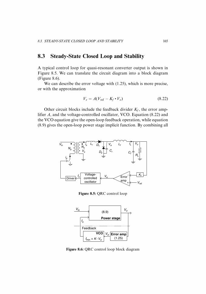
8.3 Steady-State Closed Loop and Stability
A typical control loop for quasi-resonant converter output is shown in
Figure 8.5. We can translate the circuit diagram into a block diagram
(Figure 8.6).
We can describe the error voltage with (1.25), which is more precise,
or with the approximation
Ve ¼ A(Vref � Kf. Vo) (8:22)
Other circuit blocks include the feedback divider Kf , the error amp-
lifier A, and the voltage-controlled oscillator, VCO. Equation (8.22) and
the VCO equation give the open-loop feedback operation, while equation
(8.9) gives the open-loop power stage implicit function. By combining all
Np
ip
isNs
Lr Va
Cr
LfIL Vo
CfRL
Kf
Vs
Vin D1
D2
+
−Erroramp
Voltage-controlledoscillator
Driverfs Ve
Vref
Figure 8.5: QRC control loop
Feedback
Power stage
Vin
VCO Error amp(1.25)
Vo
Ve
fs
fmin + K . Ve
(8.9)
Figure 8.6: QRC control loop block diagram
8.3. STEADY-STATE CLOSED LOOP AND STABILITY 165
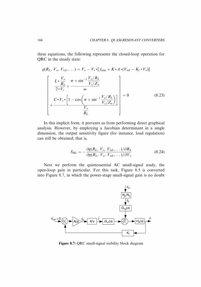
three equations, the following represents the closed-loop operation for
QRC in the steady state:
g(RL, Vo, Vref , . . . ) ¼ Vo � Vs. [ fmin þ K . A . (Vref � Kf
. Vo)]
L .Vo
RL
2 . Vs
þp þ sin�1 Vo=RL
Vs=Zn
v
þC .Vs
. 1� cos p þ sin�1 Vo=RL
Vs=Zn
� �� �Vo
RL
266666666664
377777777775¼ 0 (8:23)
In this implicit form, it prevents us from performing direct graphical
analysis. However, by employing a Jacobian determinant in a single
dimension, the output sensitivity figure (for instance, load regulation)
can still be obtained; that is,
SRL ¼ �@g(RL, Vo, Vref , . . . )=@RL
@g(RL, Vo, Vref , . . . )=@Vo
(8:24)
Next we perform the quintessential AC small-signal study, the
open-loop gain in particular. For this task, Figure 8.5 is converted
into Figure 8.7, in which the power-stage small-signal gain is no doubt
Np/Ns
Gvg(s)
++Gvf (s) He(s)
v
vin
vs
ve fK/s
Kf
A(s)Vref = 0
+−
Figure 8.7: QRC small-signal stability block diagram
166 CHAPTER 8. QUASI-RESONANT CONVERTERS

the core.This core gain is derivedby first defining a function fromequation
(8.9):
f (Vo, Vs, fs, . . . )
¼ Vo � Vs. fs .
L . Vo
2 . Vs.RL
þp þ sin�1 Vo=RL
Vs=Zn
v
þC . Vs
. 1� cos p þ sin�1 Vo=RL
Vs=Zn
� �� �Vo=RL
8>>>>>>><>>>>>>>:
9>>>>>>>=>>>>>>>;¼ 0 (8:25)
Then, the frequency-to-output modulation gain is
Gvf ¼ �@f (Vo, Vs, fs, . . . )=@fs@f (Vo, Vs, fs, . . . )=@Vo
(8:26)
And the source-to-output modulation gain is
Gvg ¼ �@f (Vo, Vs, fs, . . . )=@Vs
@f (Vo, Vs, fs, . . . )=@Vo
(8:27)
The total loop gain is then given by
T(s) ¼ �Kf. A(s) .
K
s. Gvf
.
1
RL
þ Cf. s
� ��1
Lf. sþ 1
RL
þ Cf. s
� ��1(8:28)
where K/s is the VCO gain.
8.4 Design Issues
By virtue of operating in resonant mode, the QRC design steps are
distinctively different from those for conventional forward, boost, or
flyback converters. Two fundamental constraints must be met to operate
8.4. DESIGN ISSUES 167

the resonant tank properly and take advantage of zero-current and zero-
voltage switching. Zero-current switching demands that the resonant
tank current start from zero and end at zero. This requirement can be
satisfied only by setting the maximum load current to a value that is
less than the sinusoidal peak current amplitude attainable in the resonant
tank; otherwise, the argument for arcsine is larger than 1. In other
words,
Vs
Zn
$ IL, max (8:29)
The other requirement is that the duration sum for all operation topol-
ogies equals the switching period. However, the free-wheeling time is not
bounded by a particular circuit behavior and may be set to a few percent,
say, 5%, of the switching period. Therefore, this second requirement can
be formulated as
0:95
fs, max
¼ Lr. IL, max
Vs
þp þ sin�1 IL, max
Vs=Zn
1=ffiffiffiffiffiffiffiffiffiffiffiffiffiLr
. Cr
p
þCr
.Vs. 1� cos p þ sin�1 IL, max
Vs=Zn
� �� �IL, max
(8:30)
Given the maximum load, IL, max; transferred supply, Vs ¼(Vin=Np)Ns; and switching frequency, fs, the resonant tank elements,
Lr and Cr, can be solved numerically using both equations.
8.5 Example and Dilemma
In Lui, Orugnati, and Lee [5], an example was given with Lr ¼ 1:6 mH,
Cr ¼ 0:064 mF, Lf ¼ 100 mH, Cf ¼ 10 mF, Vs ¼ 20 V, fs ¼ 150 KHz.
Theoretical computation based on the procedure of section 8.2 gives the
results of Figure 8.8. The filter inductor current is also computed. Its
result is given in Figure 8.9.
168 CHAPTER 8. QUASI-RESONANT CONVERTERS

00
1.37 . 10−6 2.75 . 10−6 4.12 . 10−6 5.5 . 10−6 6.87 . 10−600
10
20
30
40
50
6060
Vcr(t)
Tst
t
00
1.37 . 10−6 2.75 . 10−6 4.12 . 10−6 5.5 . 10−6 6.87 . 10−6
Ts
7.97.9
7.92
7.94
7.96
7.98
88
Vo(t)0
Figure 8.8: Example output; resonant capacitor and filtered output
00
0.4
0.8
1.2
1.6
22
io(t)0
00
1.37 . 10−6 2.75 . 10−6 4.12 . 10−6 5.5 . 10−6 6.87 . 10−6
Tst
Figure 8.9: Example output filter inductor current
8.5. EXAMPLE AND DILEMMA 169

However, we create a dilemma. The filter inductor current is not
really a constant, as we took the liberty to assume in section 8.2. Worst
yet, the current ripple is not insignificant.
170 CHAPTER 8. QUASI-RESONANT CONVERTERS
Chapter 9
Class-E Resonant Converter
In the course of the previous presentation, it was shown that the main
power train has numerous dissipative elements that degrade converter
efficiency. Among these dissipative factors, some are physical in nature—
for instance, winding resistance—and cannot be eliminated. Others ori-
ginating from the functional mechanism, for example, the switching
losses of power switches, may be minimized or even totally eliminated.
The switching losses arise, as shown in Wu’s Figure 9.10 [2], because
either the switch voltage rises too quickly ahead of the decreasing current
at turn-off or the switch current surges in advance of the diminishing
switch voltage at turn-on. In both cases, power pulses are created where
the switch voltage and current profiles cross each other. The switching
losses were considered an insignificant nuisance in years past, when most
switching converters operated at only tens of kilohertz. However, with
the march toward higher switching frequencies of 500 KHz and beyond,
the switching losses overtake other dissipations in importance and de-
mand attention. As a result, the concepts of zero-voltage switching (ZVS)
and zero-current switching (ZCS) were born.
Zero-voltage switching in general is implemented by placing a ca-
pacitor across the power switch (Figure 9.1). The motivation for taking
this approach is based simply on the recognition that the capacitor’s
voltages are continuous. In contrast, zero-current switching is implemen-
ted by connecting an inductor in series with the power switch, Figure 9.2.
In this case, the property of continuity of inductive current is employed.
171

Furthermore, both techniques can be enhanced by taking the advantage
of resonant circuits; that is, by adding an inductor to Figure 9.1 or a
capacitor to Figure 9.2, so a series resonant circuit, Figure 9.3, is formed.
Based on the basic form, it is only a matter of adding several more
components to yield complete power stages of the various forms. For
instance, Figure 9.4 is the most basic and popular topology of ZVS. It
was often used as a high-efficiency power amplifier and given a name,
Figure 9.1: Zero-voltage switch
Figure 9.2: Zero-current switch
Figure 9.3: Resonant switch
172 CHAPTER 9. CLASS-E RESONANT CONVERTER

Class E. However, it has also been given new life as a power converter. In
its new role, the class-E power converter, as shown in Figure 9.5(a), has
been studied extensively by Kazimierczuk [6 and 7].
However, since its inception [8] in 1975, class-E power amplifiers
and their derivatives persistently present a major challenge, or perhaps
difficulty, for circuit designers (see Sokal and Sokal [8]). This is the
daunting task of reaching a more exact analytical solution without
making some self-conflicting assumptions. For instance, when analyzing
the basic form of the class-E power stage (Figure 9.5(a)), Kazimierczuk
[6] started the process by assuming a very large input inductance and
treated the source current as constant. In addition, a high-Q condition
that enables the analysis to be carried out was also assumed. This
practice, even to this date, not only has been largely inherited in many
reports, but also has inspired other assumptions. For example, Jozwik
and Kazimierczuk [9] also assumed a pure sinusoidal branch current, ib,
in the resonant tank of Figure 9.5(a). In all, assumptions of this nature
attain expedience at the expense of accuracy. The situation is made even
worse with the switching frequency being lately pushed toward the
megahertz range, in which inductance values less than 100 microhenry
are freely used.
In other words, those assumptions invoked for the purpose of
easing the analytical procedures are being seriously challenged by the
advance of art. Therefore, to avoid the unnecessary introduction of
inaccuracy, on the one hand, and improve the understanding of resonant
DC–DC power converters, on the other, this chapter removes all as-
sumptions regarding the input inductor value, the circuit Q factor, and
the resonant branch current. Furthermore, the goal of this writing is to
obtain a more accurate and complete solution in closed form for the
converter power stage in a steady state. It is accomplished by deriving, in
L
Cq
CbLr
R
Vin
Figure 9.4: Class-E power amplifier
CHAPTER 9. CLASS-E RESONANT CONVERTER 173

section 9.1, the starting state of a steady-state switching cycle. Section 9.2
then expresses all steady-state node voltages, branch voltages, and
branch currents in compact, closed forms over one cycle. Further studies
are carried out in section 9.3 by discussing the development of DC output
formulation. Section 9.4 presents AC loop gain. The remaining sections
give the type II error amplifier, damping effects of rectifiers, and a
numerical example with the assistance of math software capable of
performing inverse Laplace transformation. A good match between the
L Lr Cb
CdCq
Vin
(a)
(b)
ia
Cq ReCe
Cbvp
Ein
L Lr ibvd
+vb−
ia
Cq ReCe
Cbvp
Ein
L Lribvd
+vb−
Loop 1 Loop 2
(c)
ia
ReCe
Cbvp
Ein
Lrib
+vb−
L
Loop 1 Loop 2
(d)
Figure 9.5: (a) Class-E resonant power converter; (b) equivalent circuit; (c) off-
time equivalent; (d) on-time equivalent
174 CHAPTER 9. CLASS-E RESONANT CONVERTER

theoretical results and the actual measurements attests to the validity of
the analytical process. The last section concludes the chapter with dis-
cussion regarding one critical assumption that is retained in the analysis.
9.1 Starting States of the Steady State
As suggested by Kazmierczuk [6], the power stage of a class-E resonant
converter can be transformed into an equivalent circuit (Figure 9.5(b)),
which delivers the same average load power as the original circuit of
Figure 9.5(a). Based on the equivalent circuit, two loop and three nodal
equations can be written respectively for the switch-off time, toff , in terms
of five state variables, ia, vd , vb, ib, and vp; that is, during toff (Figure
9.5(c)) with a designated subscript of 1, loop 1 gives
dia1
dtþ 1
L. vd1 ¼
Ein
L(9:1)
while node vd , node Cb, loop 2, and node vp give
1
Cq
. ia1 �dvd1
dt� 1
Cq
. ib1 ¼ 0
dvb1
dt� 1
Cb
. ib1 ¼ 0
� 1
Lr
. vd1 þ1
Lr
. vb1 þdib1
dtþ 1
Lr
. vp1 ¼ 0
� 1
Ce
. ib1 þdvp1
dtþ 1
Re. Ce
. vp1 ¼ 0
(9:2)
Under the condition of a steady state and at the beginning of switch-
off time, each of the five state variables bears a yet unknown starting
condition: ia10, vd10, vb10, and vp10. However, because Cq was completely
discharged in the previous switch-on time, the starting voltage, vd10, of
the switch has a null value. This reduces the number of unknowns by one,
and by taking the Laplace transformation of (9.1) and (9.2), a new
equation set is generated:
9.1. STARTING STATES OF THE STEADY STATE 175

s . Ia1 þ1
L. Vd1 þ 0þ 0þ 0 ¼ ia10 þ
Ein
L . s
1
Cq
. Ia1 � s . Vd1 þ 0� 1
Cq
. Ib1 þ 0 ¼ 0
0þ 0þ s . Vb1 �1
Cb
. Ib1 þ 0 ¼ vb10
0� 1
Lr
. Vd1 þ1
Lr
.Vb1 þ s . Ib1 þ1
Lr
. Vp1 ¼ ib10
0þ 0þ 0� 1
Ce
. Ib1 þ sþ 1
Re.Ce
� �. Vp1 ¼ vp10
(9:3)
This equation set, in matrix form, yields
Ia1(s) ¼
ia10 þEin
L . s
1
L0 0 0
0 �s 0 � 1
Cq
0
vb10 0 s � 1
Cb
0
ib10 � 1
Lr
1
Lr
s1
Lr
vp10 0 0 � 1
Ce
sþ 1
Re.Ce
�������������������
�������������������s
1
L0 0 0
1
Cq
�s 0 � 1
Cq
0
0 0 s � 1
Cb
0
0 � 1
Lr
1
Lr
s1
Lr
0 0 0 � 1
Ce
sþ 1
Re. Ce
�������������������
�������������������
(9:4)
176 CHAPTER 9. CLASS-E RESONANT CONVERTER
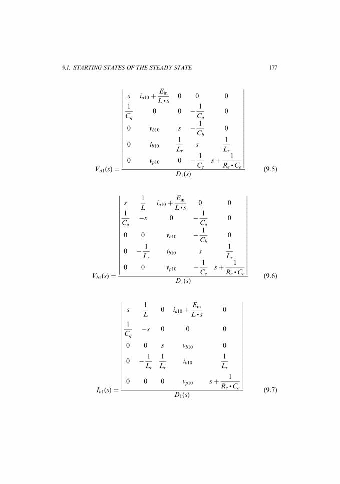
Vd1(s) ¼
s ia10 þEin
L . s0 0 0
1
Cq
0 0 � 1
Cq
0
0 vb10 s � 1
Cb
0
0 ib10
1
Lr
s1
Lr
0 vp10 0 � 1
Ce
sþ 1
Re. Ce
�������������������
�������������������D1(s)
(9:5)
Vb1(s) ¼
s1
Lia10 þ
Ein
L . s0 0
1
Cq
�s 0 � 1
Cq
0
0 0 vb10 � 1
Cb
0
0 � 1
Lr
ib10 s1
Lr
0 0 vp10 � 1
Ce
sþ 1
Re. Ce
�������������������
�������������������D1(s)
(9:6)
Ib1(s) ¼
s1
L0 ia10 þ
Ein
L . s0
1
Cq
�s 0 0 0
0 0 s vb10 0
0 � 1
Lr
1
Lr
ib10
1
Lr
0 0 0 vp10 sþ 1
Re . Ce
���������������������
���������������������D1(s)
(9:7)
9.1. STARTING STATES OF THE STEADY STATE 177

Vp1(s) ¼
s1
L0 0 ia10 þ
Ein
L . s1
Cq
�s 0 � 1
Cq
0
0 0 s � 1
Cb
vb10
0 � 1
Lr
1
Lr
s ib10
0 0 0 � 1
Ce
vp10
���������������������
���������������������D1(s)
(9:8)
The equations in Laplace transformation form can be further pro-
cessed to produce time-domain functions. For instance, the source
current (9.4) in the frequency domain can be expanded and rewritten as
Ia1(s) ¼ ia10 .H1n(s)
D1(s)þ vb10 .
H2n(s)
D1(s)þ ib10 .
H3n(s)
D1(s)þ vp10 .
H4n(s)
D1(s)
þ Ein.H5n(s)
D1(s)(9:9)
In theory, this can be inverse transformed, which brings forth
ia1(t) ¼ ia10 . h1(t)þ vb10 .h2(t)þ ib10 . h3(t)þ vp10 . h4(t)
þ Ein. h5(t) (9:10)
Therefore, at the end of switch-off time, toff ,
ia1(toff ) ¼ ia10 . h1(toff )þ vb10. h2(toff )þ ib10
. h3(toff )
þ vp10 . h4(toff )þ Ein. h5(toff ) (9:11)
By applying the same procedure against (9.5) through (9.8), the
following is generated:
vb1(toff )¼ ia10 . f1(toff )þ vb10 . f2(toff )þ ib10 . f3(toff )þ vp10 . f4(toff )
þEin. f5(toff )
(9:12)
178 CHAPTER 9. CLASS-E RESONANT CONVERTER
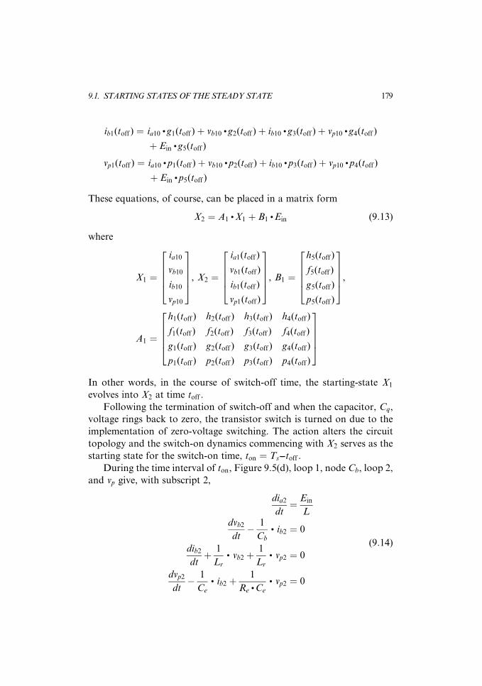
ib1(toff ) ¼ ia10 . g1(toff )þ vb10 . g2(toff )þ ib10 . g3(toff )þ vp10 . g4(toff )
þ Ein.g5(toff )
vp1(toff ) ¼ ia10 . p1(toff )þ vb10 .p2(toff )þ ib10 . p3(toff )þ vp10 . p4(toff )
þ Ein. p5(toff )
These equations, of course, can be placed in a matrix form
X2 ¼ A1 . X1 þ B1 . Ein (9:13)
where
X1 ¼
ia10
vb10
ib10
vp10
26664
37775, X2 ¼
ia1(toff )
vb1(toff )
ib1(toff )
vp1(toff )
26664
37775, B1 ¼
h5(toff )
f5(toff )
g5(toff )
p5(toff )
26664
37775,
A1 ¼
h1(toff ) h2(toff ) h3(toff ) h4(toff )
f1(toff ) f2(toff ) f3(toff ) f4(toff )
g1(toff ) g2(toff ) g3(toff ) g4(toff )
p1(toff ) p2(toff ) p3(toff ) p4(toff )
26664
37775
In other words, in the course of switch-off time, the starting-state X1
evolves into X2 at time toff .
Following the termination of switch-off and when the capacitor, Cq,
voltage rings back to zero, the transistor switch is turned on due to the
implementation of zero-voltage switching. The action alters the circuit
topology and the switch-on dynamics commencing with X2 serves as the
starting state for the switch-on time, ton ¼ Ts---toff .
During the time interval of ton, Figure 9.5(d), loop 1, node Cb, loop 2,
and vp give, with subscript 2,
dia2
dt¼ Ein
Ldvb2
dt� 1
Cb
. ib2 ¼ 0
dib2
dtþ 1
Lr
. vb2 þ1
Lr
. vp2 ¼ 0
dvp2
dt� 1
Ce
. ib2 þ1
Re. Ce
. vp2 ¼ 0
(9:14)
9.1. STARTING STATES OF THE STEADY STATE 179

Assuming the starting state for the switch-on time, Ts � toff , as
(ia20 vb20 ib20 vp20)T , the first equation of (9.14) is solved separately:
ia2(t) ¼ ia20 þEin
L. (t� toff )
� �. u(t� toff ) (9:15)
while the rest gives
Vb2(s) ¼
vb20 � 1
Cb
0
ib20 s1
Lr
vp20 � 1
Ce
sþ 1
Re. Ce
�����������
�����������. e�toff
. s
s � 1
Cb
0
1
Lr
s1
Lr
0 � 1
Ce
sþ 1
Re. Ce
�����������
�����������
(9:16)
Ib2(s) ¼
s vb20 01
Lr
ib20
1
Lr
0 vp20 sþ 1
Re. Ce
���������
���������. e�toff
. s
D2(s)(9:17)
Vp2(s) ¼
s � 1
Cb
vb20
1
Lr
s ib20
0 � 1
Ce
vp20
�����������
�����������. e�toff
. s
D2(s)(9:18)
180 CHAPTER 9. CLASS-E RESONANT CONVERTER
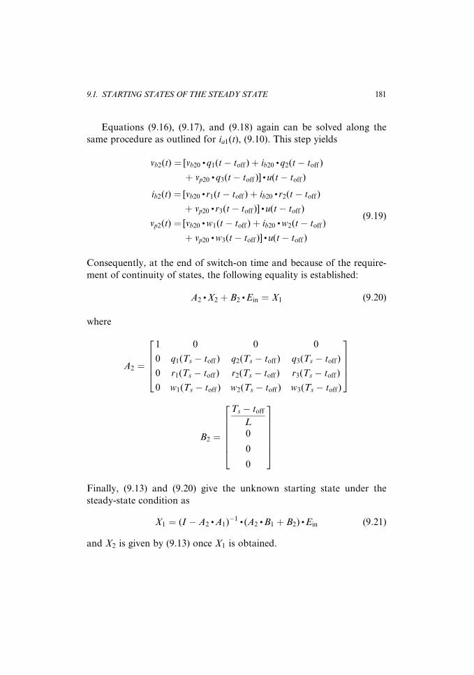
Equations (9.16), (9.17), and (9.18) again can be solved along the
same procedure as outlined for ia1(t), (9.10). This step yields
vb2(t) ¼ [vb20 .q1(t� toff )þ ib20 .q2(t� toff )
þ vp20 . q3(t� toff )] . u(t� toff )
ib2(t) ¼ [vb20 . r1(t� toff )þ ib20 . r2(t� toff )
þ vp20 . r3(t� toff )] .u(t� toff )
vp2(t) ¼ [vb20 . w1(t� toff )þ ib20 .w2(t� toff )
þ vp20 . w3(t� toff )] . u(t� toff )
(9:19)
Consequently, at the end of switch-on time and because of the require-
ment of continuity of states, the following equality is established:
A2 . X2 þ B2 . Ein ¼ X1 (9:20)
where
A2 ¼
1 0 0 0
0 q1(Ts � toff ) q2(Ts � toff ) q3(Ts � toff )
0 r1(Ts � toff ) r2(Ts � toff ) r3(Ts � toff )
0 w1(Ts � toff ) w2(Ts � toff ) w3(Ts � toff )
26664
37775
B2 ¼
Ts � toff
L
0
0
0
2666664
3777775
Finally, (9.13) and (9.20) give the unknown starting state under the
steady-state condition as
X1 ¼ (I � A2 . A1)�1 . (A2 . B1 þ B2) . Ein (9:21)
and X2 is given by (9.13) once X1 is obtained.
9.1. STARTING STATES OF THE STEADY STATE 181

9.2 Time-Domain Steady-State Solutions
With both starting states for the two distinctive time intervals available,
all branch currents and node voltages under the steady-state condition
can be expressed for just one switching cycle as
ia(t) ¼ XT1
.
h1(t)
h2(t)
h3(t)
h4(t)
2664
3775þ Ein
.h5(t)
8>><>>:
9>>=>>; . [u(t)� u(t� toff )]
þ XT2
.
1
0
0
0
26643775þ Ein
L. (t� toff )
8>><>>:
9>>=>>; . [u(t� toff )� u(t� Ts)]
vd(t) ¼ XT1
.
xd1(t)
xd2(t)
xd3(t)
xd4(t)
2664
3775þ Ein
. xd5(t)
8>><>>:
9>>=>>; . [u(t)� u(t� toff )]
vb(t) ¼ XT1
.
f1(t)
f2(t)
f3(t)
f4(t)
2664
3775þ Ein
. f5(t)
8>><>>:
9>>=>>; . [u(t)� u(t� toff )] (9:22)
þ XT2
.
0
q1(t� toff )
q2(t� toff )
q3(t� toff )
2664
3775þ Ein
L. (t� toff )
8>><>>:
9>>=>>; . [u(t� toff )� u(t� Ts)]
ib(t) ¼ XT1
.
g1(t)
g2(t)
g3(t)
g4(t)
2664
3775þ Ein
.g5(t)
8>><>>:
9>>=>>; . [u(t)� u(t� toff )]
þ XT2
.
0
r1(t� toff )
r2(t� toff )
r3(t� toff )
2664
3775þ Ein
L. (t� toff )
8>><>>:
9>>=>>; . [u(t� toff )� u(t� Ts)]
182 CHAPTER 9. CLASS-E RESONANT CONVERTER
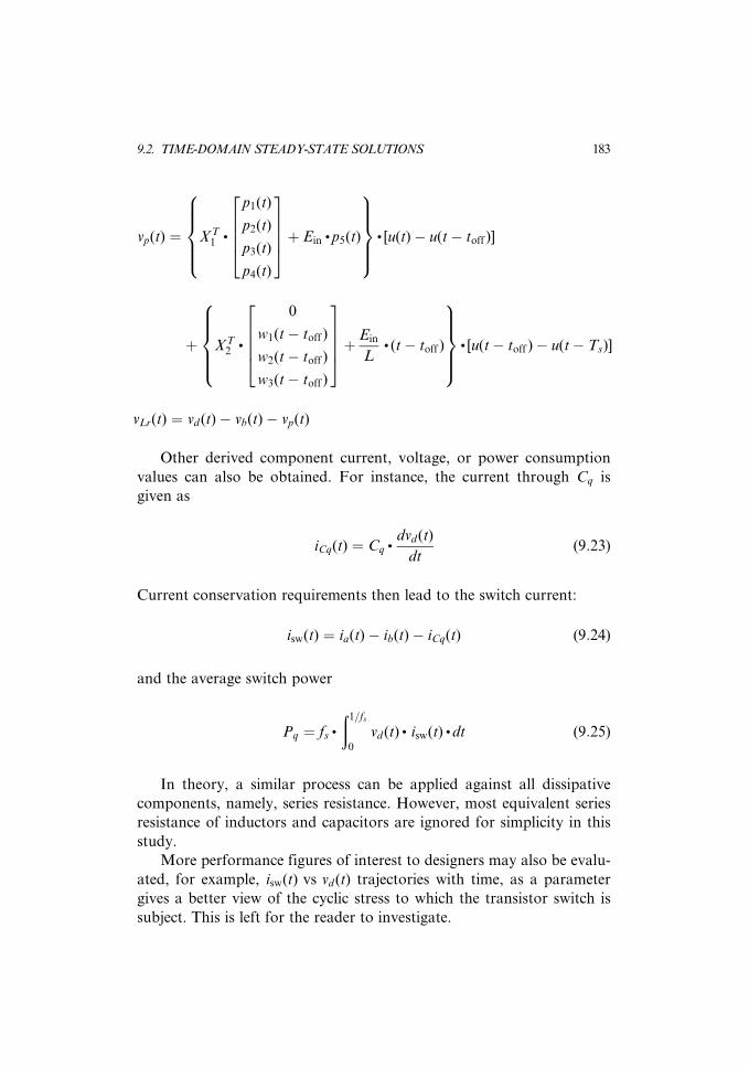
vp(t) ¼ XT1
.
p1(t)
p2(t)
p3(t)
p4(t)
26664
37775þ Ein
. p5(t)
8>>><>>>:
9>>>=>>>;
. [u(t)� u(t� toff )]
þ XT2
.
0
w1(t� toff )
w2(t� toff )
w3(t� toff )
26664
37775þ Ein
L. (t� toff )
8>>><>>>:
9>>>=>>>;
. [u(t� toff )� u(t� Ts)]
vLr(t) ¼ vd(t)� vb(t)� vp(t)
Other derived component current, voltage, or power consumption
values can also be obtained. For instance, the current through Cq is
given as
iCq(t) ¼ Cq.dvd(t)
dt(9:23)
Current conservation requirements then lead to the switch current:
isw(t) ¼ ia(t)� ib(t)� iCq(t) (9:24)
and the average switch power
Pq ¼ fs .
ð1=fs
0
vd(t) . isw(t) . dt (9:25)
In theory, a similar process can be applied against all dissipative
components, namely, series resistance. However, most equivalent series
resistance of inductors and capacitors are ignored for simplicity in this
study.
More performance figures of interest to designers may also be evalu-
ated, for example, isw(t) vs vd(t) trajectories with time, as a parameter
gives a better view of the cyclic stress to which the transistor switch is
subject. This is left for the reader to investigate.
9.2. TIME-DOMAIN STEADY-STATE SOLUTIONS 183
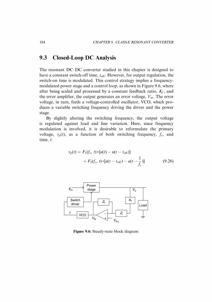
9.3 Closed-Loop DC Analysis
The resonant DC–DC converter studied in this chapter is designed to
have a constant switch-off time, toff . However, for output regulation, the
switch-on time is modulated. This control strategy implies a frequency-
modulated power stage and a control loop, as shown in Figure 9.6, where
after being scaled and processed by a constant feedback ratio, Kf , and
the error amplifier, the output generates an error voltage, Ver. The error
voltage, in turn, feeds a voltage-controlled oscillator, VCO, which pro-
duces a variable switching frequency driving the driver and the power
stage.
By slightly altering the switching frequency, the output voltage
is regulated against load and line variation. Here, since frequency
modulation is involved, it is desirable to reformulate the primary
voltage, vp(t), as a function of both switching frequency, fs, and
time, t:
vp(t) ¼ F1(fs, t) . [u(t)� u(t� toff )]
þ F2(fs, t) . [u(t� toff )� u(t� 1
fs)] (9:26)
+−
Ein
Powerstage
Switchdriver
VCO
ZfKf
Zi
Ver Verf
Vo
f
Load
Figure 9.6: Steady-state block diagram
184 CHAPTER 9. CLASS-E RESONANT CONVERTER

where
F1( fs, t)¼ [I �Y ( fs, toff ) . A1]�1 . Y ( fs, toff ) . B1þ
1
fs� toff
L
0
0
0
26666664
37777775
26666664
37777775
. Ein
8>>>>>><>>>>>>:
9>>>>>>=>>>>>>;
T
.
p1(t)
p2(t)
p3(t)
p4(t)
2664
3775þ Ein
. p5(t)
F2( fs, t) ¼ A1 . [I � Y ( fs, toff ) .A1]�1 . Y ( fs, toff ) . B1 þ
1
fs� toff
L
0
0
0
2666664
3777775
2666664
3777775
8>>>>><>>>>>:
. Ein þ B1 . Ein
)T
.
0
w1(t� toff )
w2(t� toff )
w3(t� toff )
2664
3775
Y ( fs, toff ) ¼
1 0 0 0
0 q1
1
fs� toff
� �q2
1
fs� toff
� �q3
1
fs� toff
� �
0 r1
1
fs� toff
� �r2
1
fs� toff
� �r3
1
fs� toff
� �
0 w1
1
fs� toff
� �w2
1
fs� toff
� �w3
1
fs� toff
� �
26666666664
37777777775(9:27)
Through the transformer turn ratio, n, and by including rectifier
drop, VRC , the power stage gives a DC, open-loop output voltage as a
function of switching frequency, fs:
9.3. CLOSED-LOOP DC ANALYSIS 185

VDC( fs) ¼ fs .
ð 1fs
0
(j 1n
. vp( fs, t)j � VRC) . dt (9:28)
or
VDC( fs) ¼fs
n.
ðtoff
0
jF1( fs, t)j . dtþð 1
fs
toff
jF2( fs, t)j . dt
" #� VRC (9:29)
Based on the block diagram of Figure 9.6, the closed-loop DC equation
can then be written as
A(Vref � K . VDC)GVCO þ fo
n
" ðtoff
0
jF1(A, Vref , K , VDC, GVCO, fo, t)jdt
þð 1
A(Vref�K . VDC)GVCOþfo
toff
jF2(A, Vref , K , VDC, GVCO, fo, t)jdt
#
�VRC � VDC ¼ 0 (9:30)
where A stands for the open-loop gain of the error amplifier, Vref the
command reference voltage, Kf the DC feedback factor, GVCO the voltage-
controlled-oscillator gain, and fo the minimum VCO output frequency.
As can be seen fromequation (9.30), the closed-loopDCoutput cannot
be easily expressed explicitly in terms of circuit components and param-
eters, since symbol VDC is embedded extremely deep in the second integral
and in each component function of F2( fs, t). It is therefore left in this
implicit form. However, even in these undesirable forms, more studies can
be conducted. For instance, by sweeping the switching frequency, fs, the
open-loop DC output equation (9.29) gives the output sensitivity against
the switching frequency. By the same token, (9.30) can be employed for
closed-loop output sensitivity studies. For example, although very tedious,
the output sensitivity against the VCO gain, GVCO, can be derived as
follows by first assigning the left-hand side of (9.30) a function symbol
fDC. The sensitivity figure is then given by taking the Jacobian
@VDC
@GVCO
¼ �
@fDC
@GVCO
@fDC
@VDC
(9:31)
186 CHAPTER 9. CLASS-E RESONANT CONVERTER

Similar studies, of course, can be performed for other parameters and
give the designers a better perception as to the direction where improve-
ment can be achieved and how to implement it.
9.4 Closed-Loop AC Analysis
In addition to the DC studies given in the previous section, AC small-
signal loop response can also be evaluated employing equation (9.29).
For this latter study, the small-signal gain of the power stage at low-
perturbation frequency can be described as
Gp(fs) ¼dVDC( fs)
dfs(9:32)
Thepower stage gain can thenbe incorporated into the overallAC loop
gain formulation. This last step results in the control loop gain function as
T(s) ¼ �Kf. A(s) .GVCO . Gp( fs) . Hp(s) (9:33)
Among the five factors contributing to the loop gain, all but Hp(s)
have been, or can be, dealt with easily. Here, Kf is the feedback divider
ratio, A(s) the error amplifier, GVCO the VCO linear gain, and so forth.
For the last item, and from the viewpoint of practical application, it can
be considered to be dominated by the output filter with series damping.
The damping effect is thought to come from the dynamic resistance of
the full-wave rectifier. With this in mind, the power stage transfer func-
tion Hp(s) is given as
Hp(s) ¼1
RLþ Co
. s� ��1
Lo. sþ 1
rsþ Cs
. s� ��1
þ 1RLþ Co
. s� ��1
(9:34)
where, in reference to Figure 9.5(a), rs stands for the series damping
resistance, consisting of the rectifier dynamic series resistance and the
series resistance of the output filter choke; Cs for parasitic capacitance
across the damping resistor; Lo the output filter choke; Co the output
filter capacitor; and RL the load.
9.4. CLOSED-LOOP AC ANALYSIS 187

The damping resistance of output rectifiers should be examined for
two possible cases. If the regular junction diodes are used, the dynamic
resistance can be derived by the following set of equations, representing
the junction diodes operating in the first quadrant of the I–V plane:
I(Vd) ¼ Is. (eq . Vd=k . T � 1)
rs ¼1
@I(Vd)=@Vd
(9:35)
Here, the forward current of rectifiers is expressed as a function of the
forward voltage and other fundamental constants of physics.
By the same token, if MOSFET synchronous rectifiers are used, the
damping resistance is obtained by the following two equations:
I(Vds) ¼ b . (Vgs � Vt)2 . (1� l . Vds) . tan h(a .Vds)
rs ¼1
@I(Vds)=@Vds
(9:36)
where the drain-to-source current is expressed in terms of drain-to-source
voltage, Vds, gate-to-source voltage, Vgs, and other curve-fitting param-
eters, depending on the specific device.
On the surface and in mathematical form, both appear to be similar.
However, once both dynamic resistances are plotted as a function of their
operating points (Figures 9.7 and 9.8), a critical difference clearly
00
0.15 0.3 0.45 0.60.6
00
0.4
0.8
1.2
1.6
22
rd(Vf )
Vf
Figure 9.7: Dynamic impedance of a diode
188 CHAPTER 9. CLASS-E RESONANT CONVERTER

emerges. What the plot indicates is that both devices are not necessarily
interchangeable. Designers hoping to do so should exercise caution.
9.5 Type II Amplifier
Up to this point, all factors but Kf and A(s) have been treated. In general,
the DC feedback ratio Kf is implemented easily with resistive compon-
ents and requires no further analysis. The compensation amplifier, A(s),
however deserves more attention.
To give the compensation amplifier an in-depth treatment, (9.33) is
partitioned into two groups and presented as
T(s) ¼M(s) . A(s) (9:37)
where
M(s) ¼ �K . GVCO . Gp(fs) . Hp(s) (9:38)
The modulator group, M(s), can be analyzed separately and gives a
magnitude and phase profile, as shown in Figure 9.9. Based on the modu-
lator gain (magnitude) curve and assuming the overall loop unity-gain
0
0
0.25 0.5 0.75 1 1.25 1.500
0.4
0.8
1.2
1.6
22
rd(Vds)
1.5Vds
Figure 9.8: Dynamic impedance of a MOSFET
9.5. TYPE II AMPLIFIER 189
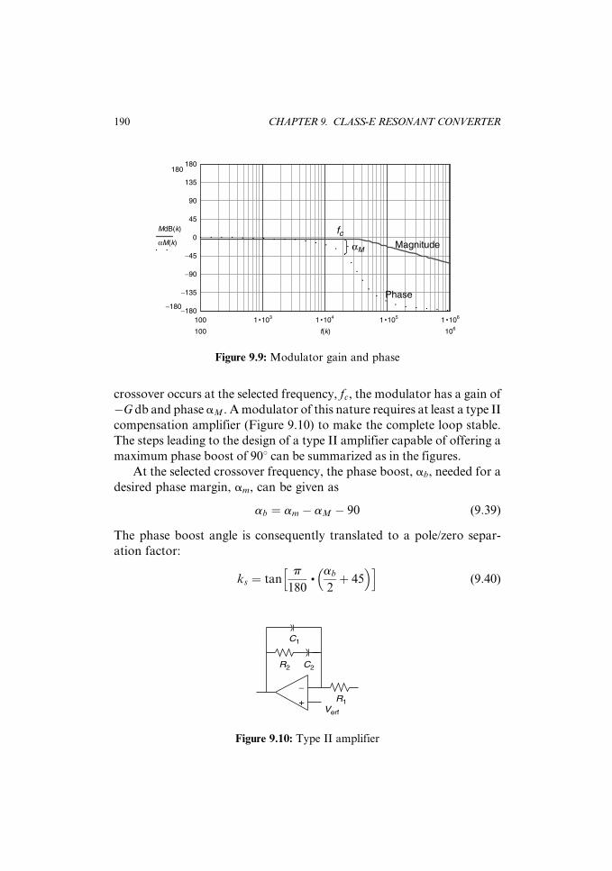
crossover occurs at the selected frequency, fc, the modulator has a gain of
�G db and phase aM . A modulator of this nature requires at least a type II
compensation amplifier (Figure 9.10) to make the complete loop stable.
The steps leading to the design of a type II amplifier capable of offering a
maximum phase boost of 908 can be summarized as in the figures.
At the selected crossover frequency, the phase boost, ab, needed for a
desired phase margin, am, can be given as
ab ¼ am � aM � 90 (9:39)
The phase boost angle is consequently translated to a pole/zero separ-
ation factor:
ks ¼ tanp
180.
ab
2þ 45
� �h i(9:40)
MdB(k)
αM(k)
f(k)
100
100
1 • 103 1 • 104 1 • 105 1 • 106
106
−180−180
−135
−90
−45
0
45
90
135
180180
fcMagnitude
Phase
αM
Figure 9.9: Modulator gain and phase
+
−
Verf
C1
R2
R1
C2
Figure 9.10: Type II amplifier
190 CHAPTER 9. CLASS-E RESONANT CONVERTER
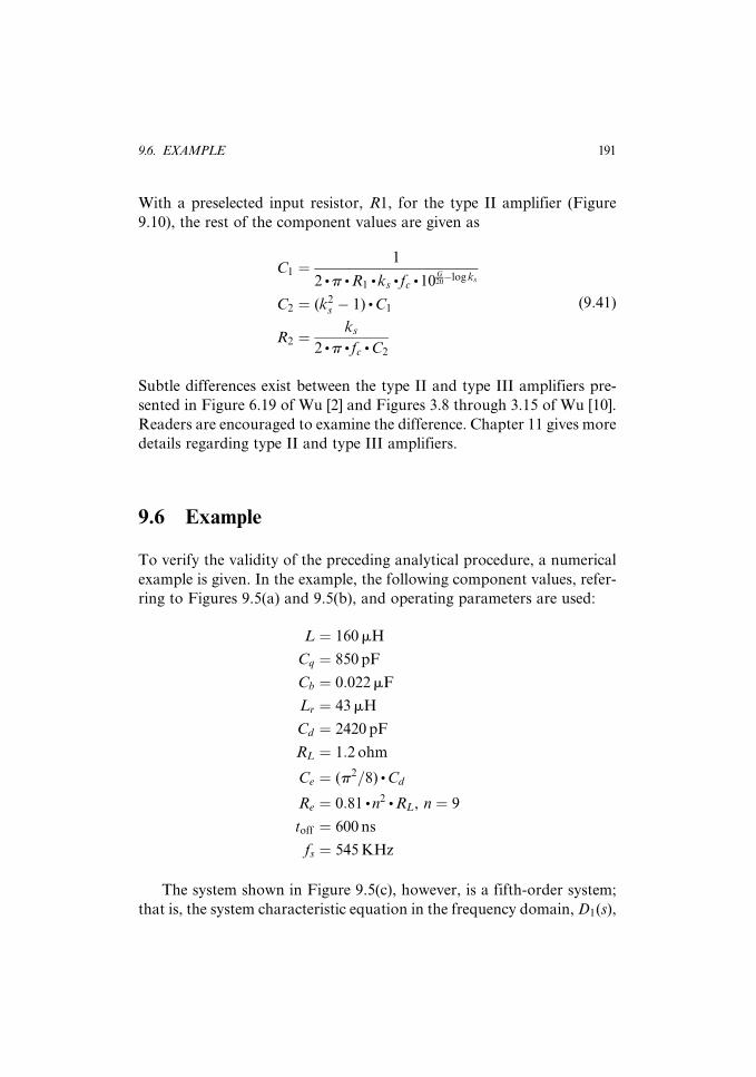
With a preselected input resistor, R1, for the type II amplifier (Figure
9.10), the rest of the component values are given as
C1 ¼1
2 . p . R1 . ks. fc . 10
G20�log ks
C2 ¼ (k2s � 1) . C1
R2 ¼ks
2 . p . fc . C2
(9:41)
Subtle differences exist between the type II and type III amplifiers pre-
sented in Figure 6.19 of Wu [2] and Figures 3.8 through 3.15 of Wu [10].
Readers are encouraged to examine the difference. Chapter 11 gives more
details regarding type II and type III amplifiers.
9.6 Example
To verify the validity of the preceding analytical procedure, a numerical
example is given. In the example, the following component values, refer-
ring to Figures 9.5(a) and 9.5(b), and operating parameters are used:
L ¼ 160 mH
Cq ¼ 850 pF
Cb ¼ 0:022 mF
Lr ¼ 43 mH
Cd ¼ 2420 pF
RL ¼ 1:2 ohm
Ce ¼ (p2=8) . Cd
Re ¼ 0:81 . n2 . RL, n ¼ 9
toff ¼ 600 ns
fs ¼ 545KHz
The system shown in Figure 9.5(c), however, is a fifth-order system;
that is, the system characteristic equation in the frequency domain, D1(s),
9.6. EXAMPLE 191

is a fifth-degree polynomial in Laplace operator, s. Furthermore, most
coefficients of the polynomial are complex combinations of circuit
components:
D1(s)¼� s5þ 1
Re. Ce
. s4þ 1
Lr
.1
Ce
þ 1
Cb
� �þ 1
Lþ 1
Lr
� �.
1
Cq
� �. s3
�
þ 1
Lr
.1
Cq
þ 1
Cb
� �þ 1
L .Cq
� �.
1
Re. Ce
. s2þ 1
L . Lr. Cq
.1
Ce
þ 1
Cb
� �. s
þ 1
L . Lr. Cq
. Cb. Re
. Ce
(9:42)
Polynomials in this form simply cannot be placed in the conventional
factored forms needed to perform inverse Laplace transformation by
hand. Therefore, all transfer functions, a total of 29 in this study, are
left in their primitive forms and MathCAD V.7 (Mathsoft, Inc.), capable
of inverse transformation, is invoked to obtain the corresponding time-
domain functions. Once this is done, the all-state transition matrix
A1, B1, A2, and B2 are hence available and eventually lead to
X1 ¼
0:799
57:329
�0:961
�68:631
2664
3775, X2 ¼
0:259
72:247
1:415
75:809
2664
3775
0
iL(t)
5 • T0 t0
0.2
0.4
0.6
0.8
1
1.2
1.4
1.6
1.8
22
Figure 9.11: Input current
192 CHAPTER 9. CLASS-E RESONANT CONVERTER
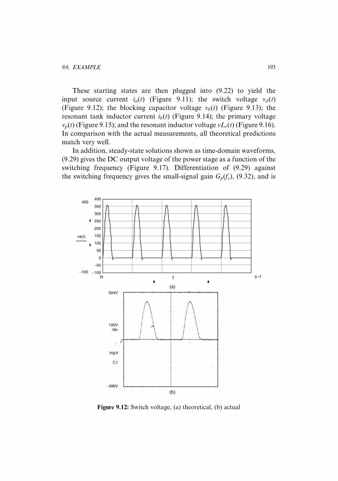
These starting states are then plugged into (9.22) to yield the
input source current ia(t) (Figure 9.11); the switch voltage vd(t)
(Figure 9.12); the blocking capacitor voltage vb(t) (Figure 9.13); the
resonant tank inductor current ib(t) (Figure 9.14); the primary voltage
vp(t) (Figure 9.15); and the resonant inductor voltage vLr(t) (Figure 9.16).
In comparison with the actual measurements, all theoretical predictions
match very well.
In addition, steady-state solutions shown as time-domain waveforms,
(9.29) gives the DC output voltage of the power stage as a function of the
switching frequency (Figure 9.17). Differentiation of (9.29) against
the switching frequency gives the small-signal gain Gp(fs), (9.32), and is
vs(t )
5 •T0t−100−100
−50
0
50
100
150
200
250
300
350
400400
(a)
t
(b)
504V
100V/div
trig'd
C1
−496V
Figure 9.12: Switch voltage, (a) theoretical, (b) actual
9.6. EXAMPLE 193

0
v bk(t )
5 • T0 t0
10
20
30
40
50
60
70
80
90
100100
Figure 9.13: Blocking capacitor voltage, theoretical and actual
i bk(t )
5 • T0 t−2−2
−1.6
−1.2
−0.8
−0.4
22
1.6
1.2
0.8
0.4
0
Figure 9.14: Resonant inductor current, theoretical and actual
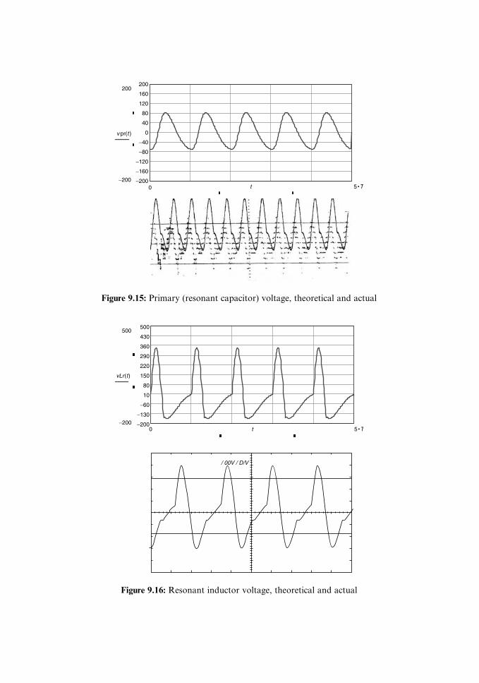
v pr(t )
5 • T0 t−200−200
−160
−120
−80
−40
0
200200
160
120
80
40
Figure 9.15: Primary (resonant capacitor) voltage, theoretical and actual
vLr(t)
0 t 5 • T−200−200−130
−60
10
80
150
220
290
360
430
500500
/ 00V / D/V
Figure 9.16: Resonant inductor voltage, theoretical and actual
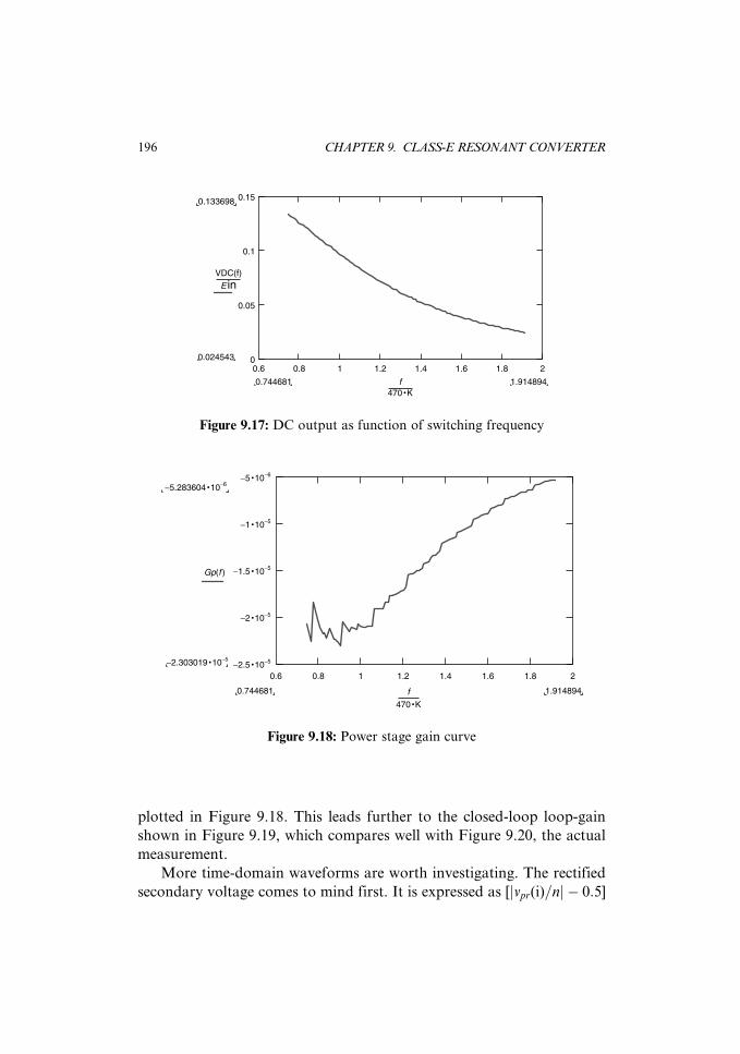
plotted in Figure 9.18. This leads further to the closed-loop loop-gain
shown in Figure 9.19, which compares well with Figure 9.20, the actual
measurement.
More time-domain waveforms are worth investigating. The rectified
secondary voltage comes to mind first. It is expressed as [jvpr(i)=nj � 0:5]
0.133698
0.024543
VDC(f)
E in
1.9148940.744681 f470 • K
0.6 0.8 1 1.2 1.4 1.6 1.8 20
0.05
0.1
0.15
Figure 9.17: DC output as function of switching frequency
Gp(f )
1.9148940.744681 f
470 • K
0.6 0.8 1 1.2 1.4 1.6 1.8 2
−5 • 10−6
−5.283604 • 10−6
−2.303019 • 10−5
−1 • 10−5
−1.5 • 10−5
−2 • 10−5
−2.5 • 10−5
Figure 9.18: Power stage gain curve
196 CHAPTER 9. CLASS-E RESONANT CONVERTER
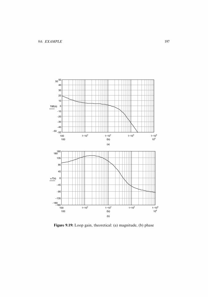
−50−50
−40
−30
−20
−10
0
10
20
30
40
5050
TdB(k)
100 1 • 103 1 • 104 1 • 105 1 • 106
106
−180
−135
−90
−45
0
45
90
135
180180
−180
αT(k)
100 f(k)
(b)
100 1 • 103 1 • 104 1 • 105 1 • 106
106100 f(k)
(a)
Figure 9.19: Loop gain, theoretical: (a) magnitude, (b) phase
9.6. EXAMPLE 197

(Figure 9.21), where the transformer turn ratio and Schottky diode drop
are included. The current through capacitor, Cq, in parallel with the
switch, is expressed as Cq[dvd(t)=dt] and its relationship with the input
current and the resonant current is given in Figure 9.22.
Last, the main switch and its associated body diode current is ex-
pressed as the input current subtracted by the resonant current and the
100 1K 10K 100KSTART 100 . 000HZ STOP 200 000.000HZ
Magnitude
Phase
REF LEVEL0 . 000dB0 . 0deg
/DIV10 . 000dB45 . 000deg
OFFSET 15 619 . 332HZMAG (A/R) −0 . 070DBMARKER 15 619 . 332HZPHASE (A/R) 32 . 015deg
Figure 9.20: Loop gain, actual
0
v sr(t )
0 t 5 • T0
2
4
6
8
10
12
14
16
18
2020
Figure 9.21: Rectified secondary voltage
198 CHAPTER 9. CLASS-E RESONANT CONVERTER
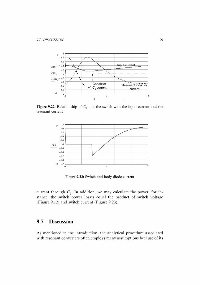
current through Cq. In addition, we may calculate the power; for in-
stance, the switch power losses equal the product of switch voltage
(Figure 9.12) and switch current (Figure 9.23).
9.7 Discussion
As mentioned in the introduction, the analytical procedure associated
with resonant converters often employs many assumptions because of its
−2
ia(t )0
ib(t )0
icq(t )0
T0 t−2
−1.6
−1.2
−0.8
−0.4
0
0.4
0.8
1.2
1.6
22
Input current
Resonant inductorcurrent
CapacitorCq current
Figure 9.22: Relationship of Cq and the switch with the input current and the
resonant current
iq(t)
Tt0−2−2
−1.6
−1.2
−0.8
−0.4
0
0.4
0.8
1.2
1.6
22
Figure 9.23: Switch and body diode current
9.7. DISCUSSION 199

complexity. Among those assumptions, some are legitimate and some
not. Assumptions considered questionable include the ideal sinusoidal
branch current, ideal sinusoidal node voltage, constant source current,
and so on. Those assumptions are removed in this study. However, one
critical assumption and its derivations are retained: the assumption of
effective power transfer consisting of only the fundamental component at
the resonant frequency, as per Kazimierczuk [6]. This assumption leads
to the establishment of the equivalent circuit of Figure 9.5(b) and the rule
of load reflection giving the effective load used in the analysis.
However, this study shows that none of the branch currents or node
voltages approaches an ideal sinusoidal waveform. This implies that
multiple harmonics are present and calls into question the validity of
power transfer at the fundamental frequency. As a result, the rule of load
reflection may also be called into question and needs to be reexamined.
By assuming an ideal sinusoidal current through the resonant inductor,
Lr, and the power transfer at the same frequency,Kazimierczuk [6] reached
the end result of the load reflection rule that givesRe ¼ 0:81n2RL, RL being
the actual load.
One then may ask, given Kazimierczuk’s [6] approach based on the
existence of just one frequency, if the load reflection rule is still applicable
for a periodic source current consisting of multiple harmonics. The answer
to this question is yes, and its justification stems from the recognition that
the load reflection rule holds for each harmonic standing alone and
consequently for all harmonics superimposed (summed). This is the rea-
son why the equivalent circuit of Figure 9.5(b) is used, even though the
resonant branch current is eventually known to be not sinusoidal.
Another matter that needs to be discussed is the validity of the
equivalent circuit shown in Figure 9.5(b). As is shown, the circuit is
valid to a large extent, but it can be improved further. The improvement
comes in the form of adding the magnetizing inductance of the trans-
former primary winding to the equivalent circuit. This step changes
Figure 9.5 to Figure 9.24. By so doing, the system order increases
by one and makes D1(s) a 68 polynomial while D2(s) becomes a 48equation. Without question, the analytical procedure associated with
this improved circuit is significantly more demanding than what has
been obtained. Moreover, several dissipative components can be added
200 CHAPTER 9. CLASS-E RESONANT CONVERTER

to Figure 9.24, resulting in Figure 9.25. This latter step does not change
the system order but it does add damping properties to the system. In
theory, this improvement makes the analysis results better represent the
actual hardware performance. Although extremely cumbersome, the
procedure may yield results that far outweigh the additional effort.
More studies are therefore possible and suggested in this regard.
L
Cq
LrCb
Re
Ein
Ce
vpvd
+vb−iaib
Lm
Figure 9.24: Adding magnetizing inductance
L LrCb
Cq Re
EinCe
vpvd
+vb−iaib
Lm
Rr Rm
Figure 9.25: Adding dissipative components
9.7. DISCUSSION 201

This page intentionally left blank

Chapter 10
AC–DC Power-FactorCorrection Supplies
Conventional single-phase AC–DC rectification (Figure 10.1) was trea-
ted in Wu [10], who showed in that analysis, as was well understood in
the past, that the input line current is pulsating and nonsinusoidal. This
implies high harmonic contents and a low power factor. The former
produces electromagnetic interferences and the latter gives rise to
low-power transfer efficiency. It is therefore imperative to reshape, by
some means, the input current such that not only is it in phase with
the rectified source voltage but also sinusoidal in its time-domain
profile with low harmonic distortion. That is the essence of power-factor
correction, PFC.
203
i(t)
v(t)
Figure 10.1: AC–DC rectifier and filter

In the old days, the objective was met by passive means, adding huge
capacitor banks to the AC line. In contrast, modern techniques approach
it through active means, employing a switch-mode converter and forcing
line current to match the line voltage. We attempt to cover the topic by
briefly going over some definition issues, then examine the fundamental
theory for boosting the PFC, the output capacitor size, the boost
inductor selection, high-power parallel operation, current sharing issues,
startup considerations, output short-circuit protection, control issues,
and three-phase PFC, in that order.
10.1 Fundamental Definition
Given a circuit (Figure 10.2) that contains passive components and
active switching devices and is driven by a single-frequency sinusoid,
the instantaneous input power is given as
p(t) ¼ v(t) . i(t) ¼ V . sin (vt) .
Xn
In. sin (n . v . tþ un), n ¼ 1,2, . . .
(10:1)
The input current is expressed as a Fourier series because of the under-
standing that it is cyclic but nonsinusoidal. We can expand the expres-
sion, which leads to
p(t) ¼ VX
n
(In. cosun
. sinvt . sin nvtþ In. sinun
. sinvt . cos nvt)
(10:2)
i(t)
v(t)Passive
andactiveload
Figure 10.2: AC–DC rectifier with a nonlinear load
204 CHAPTER 10. AC–DC POWER-FACTOR CORRECTION SUPPLIES

We then take the average of (10.2):
< p(t) >¼ VX
n
(In. cosun
. < sinvt . sinnvt > þIn. sinun
.
< sinvt . cosnvt > )
(10:3)
From the theory of orthogonal functions,
< sinvt . sinnvt > ¼½ n = 1
0 n = 2,3, . . .
�< sinvt . cosnvt > ¼ 0 n ¼ 1,2,3, . . .
(10:4)
Therefore,
< p(t) >¼ VI1 . cosu1
2¼ Vffiffiffi
2p I1ffiffiffi
2p cosu1 ¼ Vrms . I1 rms cosu1 (10:5)
This equation is the basis for the power factor, PF, definition, which
is defined as
PF ¼ < p(t) >
Vrms . irms
¼ I1 rms
irms
cosu1 ¼ kd. ku (10:6)
where ku is attributed to the angular displacement of the fundamental
current referred to the input voltage source, while kd represents current
shape distortion. For instance, given a single-phase AC source of
120 Vrms, 60 Hz, line resistance 0.5 ohm, filter capacitor 200 mF, and
expected 140 VDC output loaded at 57 ohm, the steady-state output
voltage and the rectified input line current are as shown in Figure 10.3.
The RMS (Root Mean Squared) input current is 4.45 A. That is trans-
lated to an input apparent power Vrms . irms ¼ 534W. The average power
is 351 W. The power factor is therefore 0.658.
The input line current has a sinvt component of 4.138 A and a cosvt
component of 2.158 A. It gives an RMS current at the fundamental
frequency of 3.3 A and a phase angle of u1 ¼ 27:543�. The displacement
factor is therefore ku ¼ cosu1 ¼ 0:887, while the distortion factor
kd ¼ 0:742. The power factor is kd.ku ¼ 0:658. Both computations
agree.
10.1. FUNDAMENTAL DEFINITION 205
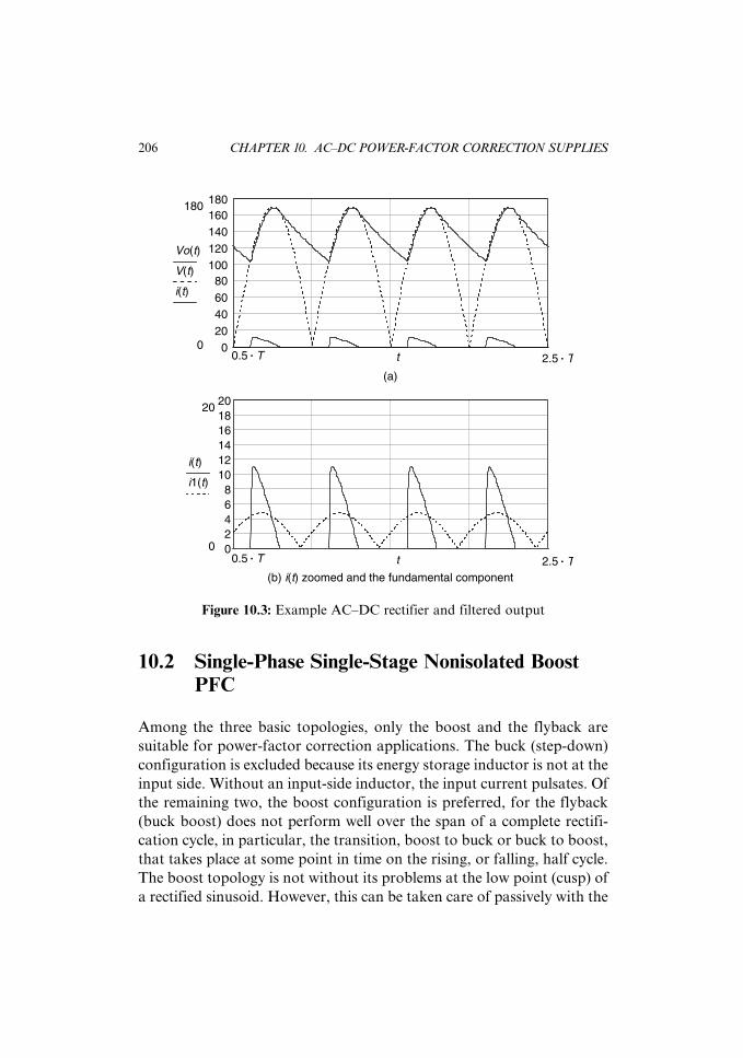
10.2 Single-Phase Single-Stage Nonisolated BoostPFC
Among the three basic topologies, only the boost and the flyback are
suitable for power-factor correction applications. The buck (step-down)
configuration is excluded because its energy storage inductor is not at the
input side. Without an input-side inductor, the input current pulsates. Of
the remaining two, the boost configuration is preferred, for the flyback
(buck boost) does not perform well over the span of a complete rectifi-
cation cycle, in particular, the transition, boost to buck or buck to boost,
that takes place at some point in time on the rising, or falling, half cycle.
The boost topology is not without its problems at the low point (cusp) of
a rectified sinusoid. However, this can be taken care of passively with the
020406080
100120140160180180
0
Vo(t)
V(t)
i(t)
2.5 . T0.5 . T t
2.5 . T0.5 . T t
(a)
02468
10121416182020
0
i(t)
i1(t)
(b) i(t) zoomed and the fundamental component
Figure 10.3: Example AC–DC rectifier and filtered output
206 CHAPTER 10. AC–DC POWER-FACTOR CORRECTION SUPPLIES

output capacitor. In contrast, it is rather difficult to assure a smooth
transition between boost and buck twice every rectified cycle. It is a
control issue. It is also an EMI (Electro-Magnetic Intereference) issue.
For those considerations, we focus on the boost PFC alone.
The boost PFC typically comes in the form of Figure 10.4, in which
the boosted output, vo(t) is fed back and sampled. The sampled output is
compared with a reference. Meanwhile, the switched line current is also
sampled, isen(t) and compared against a reduced line voltage. Both the
voltage error and the current error are multiplied. The product controls
the power switch.
By so doing, the line current is forced to follow the line voltage.
However, since a product voltage commands the power switch, one
may ask just which error is the primary control factor. In general, the
current loop has a wider bandwidth (fast), because after all, current
shaping is the goal. The voltage loop is therefore low in bandwidth
(slow), and the boosted output voltage is expected to carry significant
ripple at twice the line frequency. In the next section, we attempt to size
the output capacitor.
10.3 Output Capacitor Size
To formulate and understand the mechanism of a boost PFC, Figure
10.4 is simplified to Figure 10.5. In the figure, the input current is
Passiveand
activeload
i(t) v(t)
k
isen(t)
X
vo(t)
kf
Vref
Figure 10.4: Boost PFC
10.3. OUTPUT CAPACITOR SIZE 207

assumed to be well controlled and exhibits a sinusoid shape in phase with
the line voltage. The input power is therefore given as
pin(t) ¼ffiffiffi2p
Vrmsj sinvtj .ffiffiffi2p
Irmsj sinvtj ¼ VrmsIrms(1� cos2vt) (10:7)
If the PFC is assumed to have a conversion efficiency h, the output
power is given by
po(t) ¼ io(t) . Vo ¼ h . VrmsIrms(1� cos2vt) (10:8)
or
io(t) ¼h . VrmsIrms(1� cos2vt)
Vo
¼ Io �h . VrmsIrms
Vo
cos2vt (10:9)
Clearly, the PFC output current consists of two components, the load
current Io and the capacitor current. The latter is seen to run at twice the
line frequency. As a matter of fact, (10.8) yields an average power
< po(t) >¼ h . Vrms . Irms ¼ load power. The term running at twice the
line frequency yields a zero average. We can integrate the capacitor
current, the second term on the right-hand side of (10.9), and obtain
the PFC output ripple voltage as
vo(t) ¼1
C
ðh .VrmsIrms
Vo
cos2vtð Þdt ¼ h . VrmsIrms
2 . v . C . Vo
sin (2vtþ p) (10:10)
Given a requirement on the ripple magnitude, dvo, the output capacitor
size can be estimated using (10.10).
i(t)
v(t) Passiveand
activeload
PFCio(t) VoIo
C
Figure 10.5: Simplified boost PFC
208 CHAPTER 10. AC–DC POWER-FACTOR CORRECTION SUPPLIES

C ¼ h . VrmsIrms
2 . v . dvo. Vo
(10:11)
In all, the key waveforms for a PFC power stage can be summarized as the
following, given Vrms ¼ 120 V, output power 2000 W, and output voltage
210 V. Figures 10.6 through 10.9 present a graphic demonstration of this.
0
40
80
120
160
200200
0
v(t)
i(t)
Tt0
Figure 10.6: Input line voltage and current
0
1000
2000
3000
4000
50005 ⋅ 103
0
pi(t)
Pav
Tt0
Figure 10.7: Input instantaneous power and average power
0
5
10
15
20
2525
0
io(t)
Io
T0 t
Figure 10.8: Output current and load current
10.3. OUTPUT CAPACITOR SIZE 209

10.4 DCM Boost Inductor Selection
Boost PFCs’ inductor may operate in two modes—DCM and CCM. In
DCM, the pulsating inductor current looks like Figure 10.10, in which
the triangular current peaks follow the sinusoid contour and the rectified
input voltage.
We first give a detailed examination for one typical current pulse,
Figure 10.11, under the assumption of constant switch-on time, ton.
0
60
120
180
240
300300
0
vo(t )
Vo
Tt0
Figure 10.9: Output voltage
Figure 10.10: Inductor current (solid line) in DCM
ton td
Ts
Ipk
Figure 10.11: Inductor current pulse
210 CHAPTER 10. AC–DC POWER-FACTOR CORRECTION SUPPLIES

If that is the operation mode, the inductor current peak is expressed as
Ipk ¼ffiffiffi2p
Vrms sinvtj jL
. ton ¼Vin sinvtj j
L. ton (10:12)
At first glance, (10.12) seems to indicate a perfect sinusoidal line current.
However, the equation is deceiving. We recall from (10.3) that it is the
average that counts. It turns out that the average of (10.12) is distorted
and consists of multiple harmonics. We shall try to prove the assertion.
First, the volt–second balance demands
td ¼Vin sinvtj j . ton
Vo � Vin sinvtj j ¼L . Ipk
Vo � Vin sinvtj j (10:13)
The inductor current’s average is then given by
< iL(t) >¼ Ipk(ton þ td)
2 . Ts
(10:14)
The equation can be easily rewritten in an intermediate step as
< iL(t) > ¼ Vin sinvtj j . ton
2 .L . Ts
ton þVin sinvtj j . ton
Vo � Vin sinvtj j
� �
¼ Vin sinvtj j . t2on
2 .L . Ts
1þ Vin sinvtj jVo � Vin sinvtj j
� �(10:15)
We can gain more insight if (10.15) is placed in the following form:
< iL(t) > ¼ Vo. t2on
2 .L . Ts
1þ
Vin
Vo
sinvtj j
1� Vin
Vo
sinvtj j
0BB@
1CCAVin
Vo
sinvtj j
¼ Vo. t2on
2 .L . Ts
1þ a . sinvtj j1� a . sinvtj j
� �a sinvtj j
¼ Vo. t2on
2 .L . Ts
a
1� a . sinvtj j
� �sinvtj j (10:16)
10.4. DCM BOOST INDUCTOR SELECTION 211
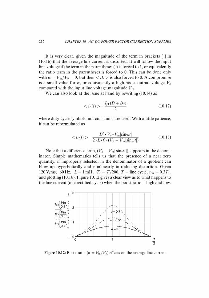
It is very clear, given the magnitude of the term in brackets [ ] in
(10.16) that the average line current is distorted. It will follow the input
line voltage if the term in the parentheses ( ) is forced to 1, or equivalently
the ratio term in the parentheses is forced to 0. This can be done only
with a ¼ Vin=Vo ¼ 0, but then < iL > is also forced to 0. A compromise
is a small value for a, or equivalently a high-boost output voltage Vo
compared with the input line voltage magnitude Vin.
We can also look at the issue at hand by rewriting (10.14) as
< iL(t) >¼ Ipk(DþD2)
2(10:17)
where duty-cycle symbols, not constants, are used. With a little patience,
it can be reformulated as
< iL(t) >¼ D2 . Vo. Vin sinvtj j
2 .L . fs . (Vo � Vin sinvtj j) (10:18)
Note that a difference term, (Vo � Vinj sinvtj), appears in the denom-
inator. Simple mathematics tells us that the presence of a near zero
quantity, if improperly selected, in the denominator of a quotient can
blow up hyperbolically and nonlinearly introducing distortion. Given
120 Vrms, 60Hz, L ¼ 1 mH, Ts ¼ T=200, T ¼ line cycle, ton ¼ 0:3Ts,
and plotting (10.16), Figure 10.12 gives a clear view as to what happens to
the line current (one rectified cycle) when the boost ratio is high and low.
0
1
2
33
0
Iav V in0.1
, t
, t
, t
Iav V in0.5
Iav V in0.7
T2
0 t
a = 0.1
a = 0.5
a = 0.7
Figure 10.12: Boost ratio (a ¼ Vin=Vo) effects on the average line current
212 CHAPTER 10. AC–DC POWER-FACTOR CORRECTION SUPPLIES

Evidently, a constant on time, ton, or constant duty cycle, D, at the
selected switching frequency, fs, is not the best strategy. Well, then, what
can be done to improve the situation? We know what we want: the
average line current proportional to and in phase with the line voltage;
that is, making
< iL(t) >¼ D2 . Vo. Vin sinvtj j
2 . L . fs . (Vo � Vin sinvtj j) ¼ k . Vin sinvtj j (10:19)
where k is a constant. It is equivalent to saying
k ¼ D2 . Vo
2 . L . fs . (Vo � Vin sinvtj j) (10:20)
In other words, instead of being a constant, the duty cycle is
D ¼
ffiffiffiffiffiffiffiffiffiffiffiffiffiffiffiffiffiffiffiffiffiffiffiffiffiffiffiffiffiffiffiffiffiffiffiffiffiffiffiffiffiffiffiffiffiffiffiffiffiffiffiffiffiffiffiffiffi2 . k .L . fs . (Vo � Vin sinvtj j)
Vo
s¼
ffiffiffiffiffiffiffiffiffiffiffiffiffiffiffiffiffiffiffiffi2 . k . L . f
Vo
s ffiffiffiffiffiffiffiffiffiffiffiffiffiffiffiffiffiffiffiffiffiffiffiffiffiffiffiffiffiffiffiVo � Vin sinvtj j
p(10:21)
That is, the duty cycle tracks the square root of the instantaneous output
and input difference. The correction factor, the second square root, has
the form of Figure 10.13.
Up to this point in this section, we have not dealt with the determin-
ation of inductor size. Fortunately, (10.13) and (10.21) together point out
0 20 40 60 80 100 120 140 160 180 2000
0.2
0.4
0.6
0.8
11
0
Dc(V in)
2000 V in
Figure 10.13: Line-voltage-corrected duty cycle
10.4. DCM BOOST INDUCTOR SELECTION 213

where we should be heading. We recognize that the sum of ton and td in
Figure 10.11 must be less than Ts:
ton þ td ¼ ton 1þ Vin sinvtj jVo � Vin sinvtj j
� �#Ts (10:22)
or
DVo
Vo � Vin sinvtj j
� �#1 (10:23)
Replacing D with (10.21), we get
ffiffiffiffiffiffiffiffiffiffiffiffiffiffiffiffiffiffiffiffiffiffiffiffiffiffiffiffiffiffiffiffiffiffiffiffiffiffiffiffiffiffiffiffiffiffiffiffiffiffiffiffiffiffiffiffiffi2 .k . L . fs . (Vo � Vin sinvtj j)
Vo
sVo
Vo � Vin sinvtj j
� �#1 (10:24)
or
L #1� a sinvtj j
2 . k . fs(10:25)
Clearly, given a selected boost ratio a, the upper bound of the boost
inductor is given as
Lmax #1� a
2 .k . fs(10:26)
Equation (10.26) ensures that the DCM is maintained throughout every
rectified cycle.
10.5 CCM Boost Inductor Selection
In CCM operation, the boost inductor current looks like Figure 10.14. It
is bounded by two sinusoids.
214 CHAPTER 10. AC–DC POWER-FACTOR CORRECTION SUPPLIES

Unlike the DCM case, the selection process for the CCM boost
inductor is less clear-cut. The most uncertain task in the process is the
step selecting the ripple current magnitude. Before we proceed, we look
at an interesting property of boost topology in CCM. The time-varying
ripple current magnitude can be expressed as
di(t) ¼ Vin sinvtj jDL . fs
¼ Vin sinvtj jL . fs
1� Vin sinvtj jVo
� �(10:27)
A simple calculus operation shows that the ripple magnitude reaches a
maximum when the instantaneous input voltage equals one half of the
output. At that instant, the ripple current magnitude equals
dimax ¼Vo
4 . L . fs(10:28)
This gives the ripple current magnitude an interesting profile over one
rectified cycle, as shown in Figure 10.15. It reaches maximum twice if the
conditions are right.
Given a required output power, Po, and conversion efficiency, h, the
input average current is
iav(t) ¼ffiffiffi2p
. Po
Vrms . hsinvtj j ¼ Ipk sinvtj j (10:29)
if we assume that the ripple current is riding on the average. The instan-
taneous input current is enveloped by
Figure 10.14: Boost inductor current in CCM
10.5. CCM BOOST INDUCTOR SELECTION 215

i(t) ¼ iav(t)�di(t)
2
¼ffiffiffi2p
. Po
h . Vrms
� Vin
2L . fs1� Vin sinvtj j
Vo
� �( )sinvtj j (10:30)
Ideally, for CCM operation, the instantaneous current during the half
cycle never reaches zero. This condition requires
ffiffiffi2p
. Po
h . Vrms
� Vin
2L . fs1� Vin sinvtj j
Vo
� �$ 0 (10:31)
That is,
Lmin $h . V 2
rms
2 . Po. fs
1�ffiffiffi2p
.Vrms sinvtj jVo
!(10:32)
For practical considerations,
Lmin $h .V 2
rms
2 . Po. fs
(10:33)
0 0.0021 0.0042 0.0063 0.00830
5
10
15
2020
0
d i(t )
T0 t
Figure 10.15: Ripple current magnitude in one half cycle
216 CHAPTER 10. AC–DC POWER-FACTOR CORRECTION SUPPLIES

10.6 High-Power PFC and Load Sharing
As of now, most single-phase boost PFC power supplies available as
commercial, off-the-shelf modules offer no more than 1 KW. To obtain
high power, for instance, 10 KW, multiple modules are placed in parallel
with active forward current control to assure load current sharing
(Figure 10.16).
But the forward current control alone does not guarantee return
current balance among modules. In addition, balance resistors,
R1, R2, . . . , Rn, are also placed on the load return line to further ensure
load sharing. Yet, as shown, the scheme still has a major detriment. The
switched currents of individual modules do not return properly. They
cross flow as shown (solid dark line, for example) in the figure. The
defect disrupts both current shaping sensing and load return current
balance and eventually leads to failure.
R 1i1i1
V
VFull-wave
bridgerectifier
Line currentshaping
controller
Current-sharing
controller
R2i2i2
VLine current
shapingcontroller
Current-sharing
controller
Rninin
VLine current
shapingcontroller
Current-sharing
controller
PFC1
PFC2
PFCn
Load
Figure 10.16: Multiple PFCs in parallel with current sharing
10.6. HIGH-POWER PFC AND LOAD SHARING 217

R1
i 1i 1
V
VF
ull-w
ave
brid
gere
ctifi
er
Line
cur
rent
shap
ing
cont
rolle
r
Cur
rent
-sh
arin
gco
ntro
ller
R2
i 2i 2
i 2
VLi
ne c
urre
ntsh
apin
gco
ntro
ller
Cur
rent
-sh
arin
gco
ntro
ller
Rn
i ni n
VLi
ne c
urre
ntsh
apin
gco
ntro
ller
Cur
rent
-sh
arin
gco
ntro
ller
PF
C1
PF
C2
PF
Cn
D1
D2 Dn
Load
Fig
ure
10.1
7:Im
pro
ved
load
retu
rncu
rren
tbala
nce
218 CHAPTER 10. AC–DC POWER-FACTOR CORRECTION SUPPLIES

The destructive crosstalk can be remedied by incorporating a unidi-
rectional device (US Patent 6,703,946)—a diode—in series with each
balance resistor, shown in Figure 10.17. By so doing, the switch current
of each module is isolated and load current sharing is assured, including
return current equalization and unidirectionality.
Figure 10.18 gives a simple current-sharing controller in which the
‘‘current-share’’ signal, equal to (total load current)/(parallel module
number), is common to all controllers while the output current is
summed via the diode ORing. A total load current sensor follows the
summing diodes and provides the ‘‘current share.’’
The current-sharing controller, as given, suffers a minor deficiency.
The current sensor is the combination of an in-line resistor, Rsen, and the
base-emitter junction of a bipolar transistor. Aside from power dissipation
acrossRsen, aminimumoutput current in the formof (current� resistance)
is required to forward bias the bipolar transistor’s base-emitter junction.
Prior to this condition, the current-sharing control loop is essentially open,
because the bipolar transistor is not conducting. The emitter resistor may
be removed or a base resistor may be added. Either way, some minimum
voltage must be present to overcome the base-emitter junction. However,
at low loads, precise current sharing may not be so imperative. In that case,
the total circuit can afford to have some current controllers not operating.
Under heavy loads, it would not be an issue.
+
−
Input Output
Currentshare
Rsen
Figure 10.18: Current-sharing controller
10.6. HIGH-POWER PFC AND LOAD SHARING 219

10.7 Surge Protection
The circuit as given in Figure 10.16 has one more problem which is quite
serious during initial turn-on if a capacitive load also is present. The
mechanism of concern can be described as follows. Note that all front-
end PFCs have an output capacitor. And, in general practice, PFCs are
turned on and ready prior to turning on the current-sharing controllers.
However, the load capacitors are generally discharged with zero starting
voltage. At the moment the current-sharing controllers commence con-
duction, surge currents result in an instantaneous redistribution of the
existing charge in all PFC output capacitors to the load capacitors. The
resulting surge may easily overstress the main current-sharing controller
element, the MOSFET.
There are numerous ways to protect against such a potentially de-
structive condition. Figure 10.19 shows a current-sharing controller with
a synchronous soft start from a master command. Prior to turning on,
the soft-start command places a 5-volt bias voltage at the noninverting
input of the error amplifier. By so doing, the bipolar npn-transistor is
fully on and the main MOSFET is shut off. At the commencement of the
soft start, the soft-start capacitor slowly releases the bias voltage and the
main MOSFET builds up conduction gradually.
+
−
Input Output
Currentshare
Rsen
5V
Softstart
Figure 10.19: Current-sharing controller with soft start
220 CHAPTER 10. AC–DC POWER-FACTOR CORRECTION SUPPLIES
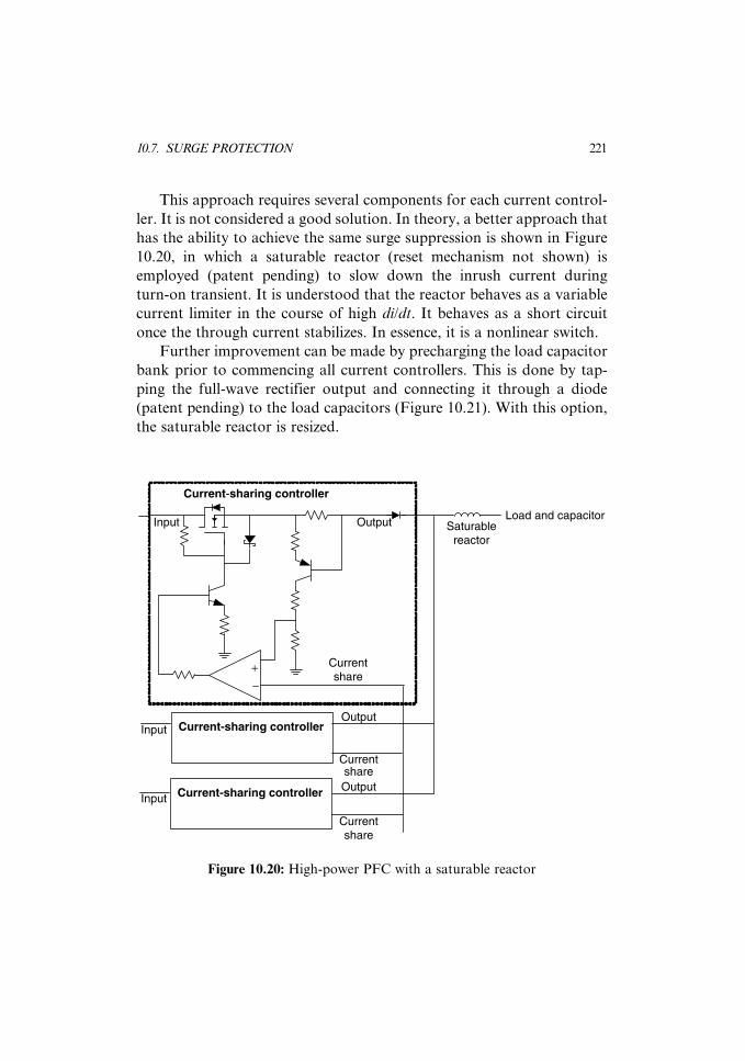
This approach requires several components for each current control-
ler. It is not considered a good solution. In theory, a better approach that
has the ability to achieve the same surge suppression is shown in Figure
10.20, in which a saturable reactor (reset mechanism not shown) is
employed (patent pending) to slow down the inrush current during
turn-on transient. It is understood that the reactor behaves as a variable
current limiter in the course of high di/dt. It behaves as a short circuit
once the through current stabilizes. In essence, it is a nonlinear switch.
Further improvement can be made by precharging the load capacitor
bank prior to commencing all current controllers. This is done by tap-
ping the full-wave rectifier output and connecting it through a diode
(patent pending) to the load capacitors (Figure 10.21). With this option,
the saturable reactor is resized.
Current-sharing controller
Current-sharing controller Output
Output
Input
Input
Currentshare
Currentshare
Current-sharing controller
+−
Input Output
Currentshare
Load and capacitorSaturable
reactor
Figure 10.20: High-power PFC with a saturable reactor
10.7. SURGE PROTECTION 221
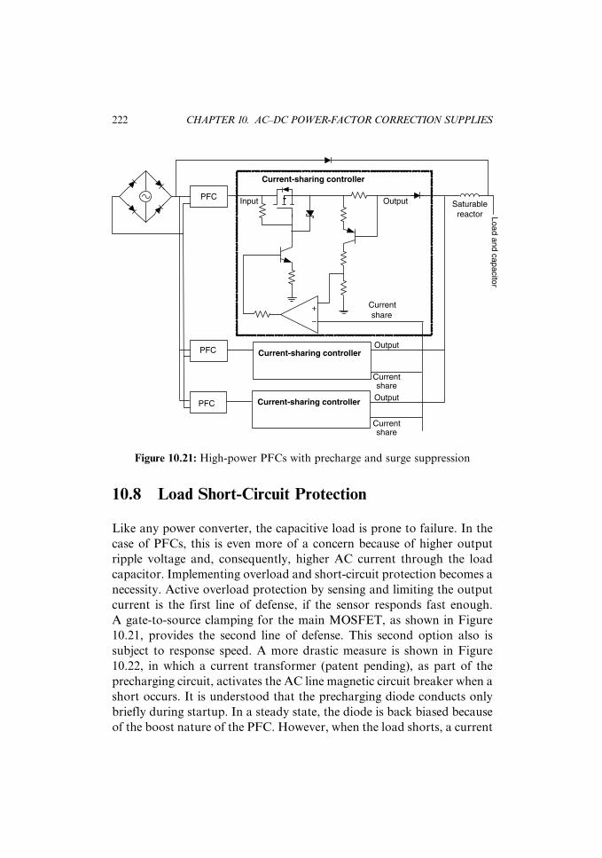
10.8 Load Short-Circuit Protection
Like any power converter, the capacitive load is prone to failure. In the
case of PFCs, this is even more of a concern because of higher output
ripple voltage and, consequently, higher AC current through the load
capacitor. Implementing overload and short-circuit protection becomes a
necessity. Active overload protection by sensing and limiting the output
current is the first line of defense, if the sensor responds fast enough.
A gate-to-source clamping for the main MOSFET, as shown in Figure
10.21, provides the second line of defense. This second option also is
subject to response speed. A more drastic measure is shown in Figure
10.22, in which a current transformer (patent pending), as part of the
precharging circuit, activates the AC line magnetic circuit breaker when a
short occurs. It is understood that the precharging diode conducts only
briefly during startup. In a steady state, the diode is back biased because
of the boost nature of the PFC. However, when the load shorts, a current
Current-sharing controller
Current-sharing controller Output
Output
Currentshare
Currentshare
Current-sharing controller
+
−
Input Output
Currentshare
Load and capacitor
Saturablereactor
PFC
PFC
PFC
Figure 10.21: High-power PFCs with precharge and surge suppression
222 CHAPTER 10. AC–DC POWER-FACTOR CORRECTION SUPPLIES

spike develops rapidly through the diode. A portion of that current may
trigger the AC circuit breaker and cut off the AC supply.
10.9 Three-Phase PFC
As shown in Figure 10.7, the input power for a single-phase PFC pulsates
at twice the line frequency. The situation can be improved with three-
phase configuration that offers constant input power. Figure 10.23 gives
three individual phases and the sum.
However, implementing the three-phase PFC is not all rosy. The
main difficulty arises in routing the neutral terminal for a Y-connected
sourcing transformer, which happens to be the most popular isolation
transformer available. Here is how the problem sneaks in.
Current-sharing controller
Current-sharing controller Output
Output
Currentshare
Currentshare
Current-sharing controller
+−
Input Output
Currentshare
Load and capacitor
Saturablereactor
PFC
PFC
PFC
Figure 10.22: High-power PFCs with short-circuit protection
10.9. THREE-PHASE PFC 223
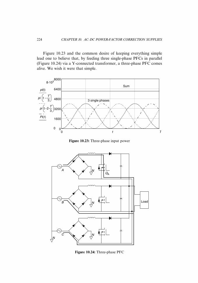
Figure 10.23 and the common desire of keeping everything simple
lead one to believe that, by feeding three single-phase PFCs in parallel
(Figure 10.24) via a Y-connected transformer, a three-phase PFC comes
alive. We wish it were that simple.
0
1600
3200
4800
6400
80008-103
0
pi(t)
pi tT3
−
pi t 2T3
⋅−
Pi(t )
T0 t
Sum
3 single phases
Figure 10.23: Three-phase input power
Load
NN
N
NA
C
B
QA
Figure 10.24: Three-phase PFC
224 CHAPTER 10. AC–DC POWER-FACTOR CORRECTION SUPPLIES
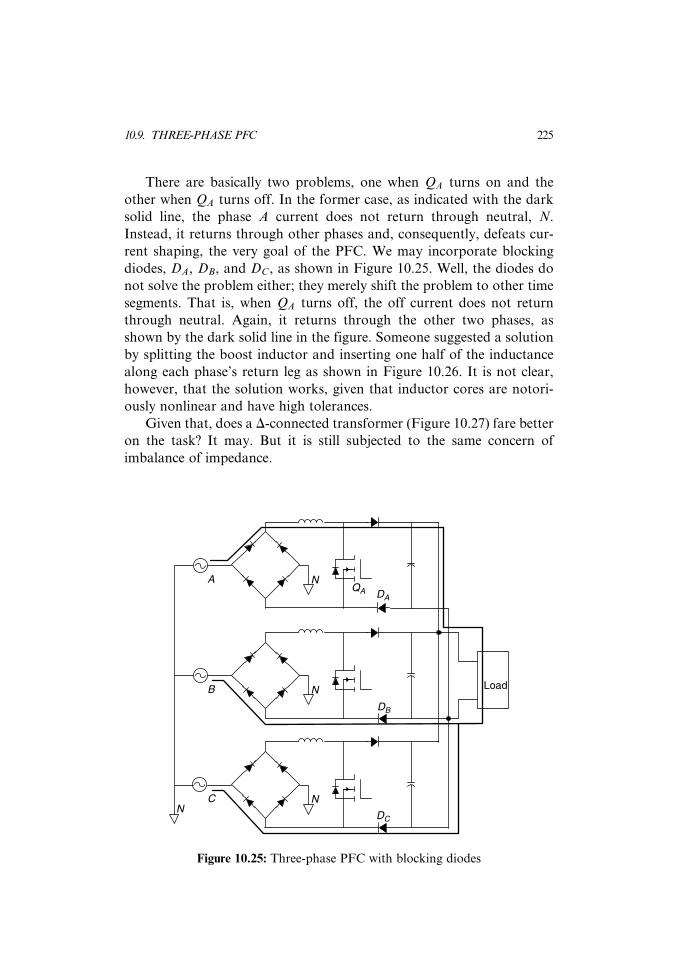
There are basically two problems, one when QA turns on and the
other when QA turns off. In the former case, as indicated with the dark
solid line, the phase A current does not return through neutral, N.
Instead, it returns through other phases and, consequently, defeats cur-
rent shaping, the very goal of the PFC. We may incorporate blocking
diodes, DA, DB, and DC , as shown in Figure 10.25. Well, the diodes do
not solve the problem either; they merely shift the problem to other time
segments. That is, when QA turns off, the off current does not return
through neutral. Again, it returns through the other two phases, as
shown by the dark solid line in the figure. Someone suggested a solution
by splitting the boost inductor and inserting one half of the inductance
along each phase’s return leg as shown in Figure 10.26. It is not clear,
however, that the solution works, given that inductor cores are notori-
ously nonlinear and have high tolerances.
Given that, does a D-connected transformer (Figure 10.27) fare better
on the task? It may. But it is still subjected to the same concern of
imbalance of impedance.
Load
NN
N
NA
C
B
QA DA
DB
DC
Figure 10.25: Three-phase PFC with blocking diodes
10.9. THREE-PHASE PFC 225
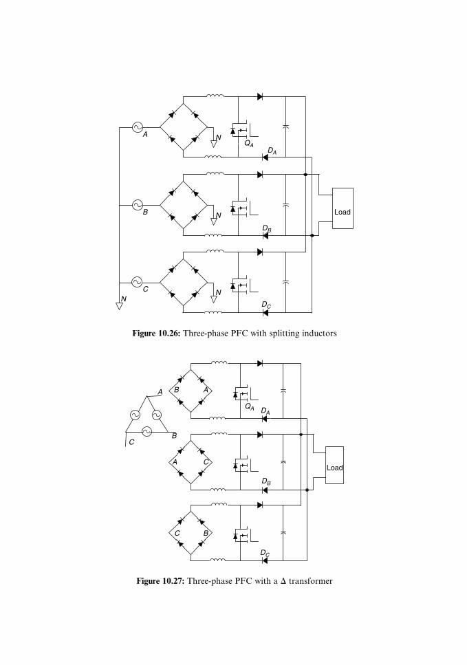
Load
NN
N
NA
C
B
QADA
DB
DC
Figure 10.26: Three-phase PFC with splitting inductors
A
CB
Load
QA DA
DB
DC
A
A
B
B
C
C
Figure 10.27: Three-phase PFC with a D transformer

So far, all three-phase configurations presented require numerous
duplicities of circuits and components. The situation is undesirable.
Something better should be available. This is what Figure 10.28, from
Tu and Chen [11], offers. It possesses simplicity and fewer parts. For the
rest of the chapter, we give this interesting scheme thorough coverage.
This highly innovative scheme effectively uses a very important as-
pect of three-phase inputs, Ea, Eb, and Ec. We can appreciate the obser-
vation better if we examine the three inputs (Figure 10.29) in which the
input time frame is partitioned into six segments.
Figure 10.28 also uses a unique, nonstandard component symbol,
such as Sab. It represents a bidirectional switch as shown in Figure 10.30.
Now, we examine the switch function in detail during T1, when the
relevant switches turn on or off. From Figure 10.29, it is clear that switch
Sab is not needed. In other words, during T1, the power plant looks like
Figure 10.31.
DaT DbT DcT
DaB DbB DcB
Ea
Eb
Ec Vc
Vb
Va
ScaSbc
Sab
Vo
ia
ib
ic
Opto Vfb
Figure 10.28: Power stage of a novel three-phase PFC
T3T2T1 T4 T5 T6
Va Vb Vc
−200−150−100
−500
50100150
200200
−200
va(t)
vb(t)
vc(t)
Tt0
Figure 10.29: Three-phase timing and partition
10.9. THREE-PHASE PFC 227
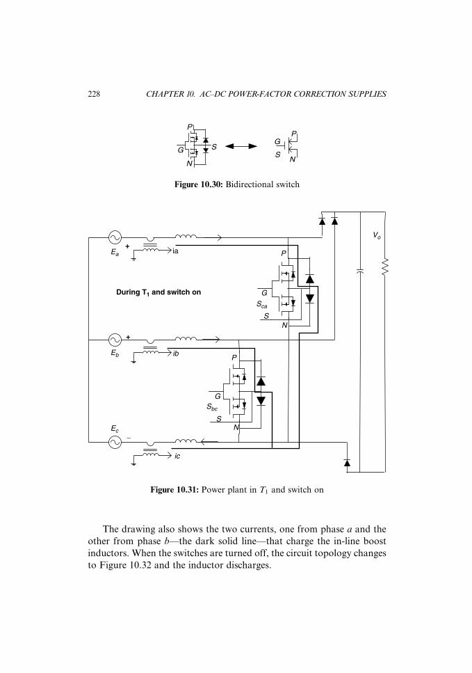
The drawing also shows the two currents, one from phase a and the
other from phase b—the dark solid line—that charge the in-line boost
inductors. When the switches are turned off, the circuit topology changes
to Figure 10.32 and the inductor discharges.
G
P
N
SG
P
NS
Figure 10.30: Bidirectional switch
Ea
Eb
Ec
Vo
Sbc
P
N
Sca
P
N
ia
ic
ib
G
G
S
S
During T1 and switch on
+
+
−
Figure 10.31: Power plant in T1 and switch on
228 CHAPTER 10. AC–DC POWER-FACTOR CORRECTION SUPPLIES
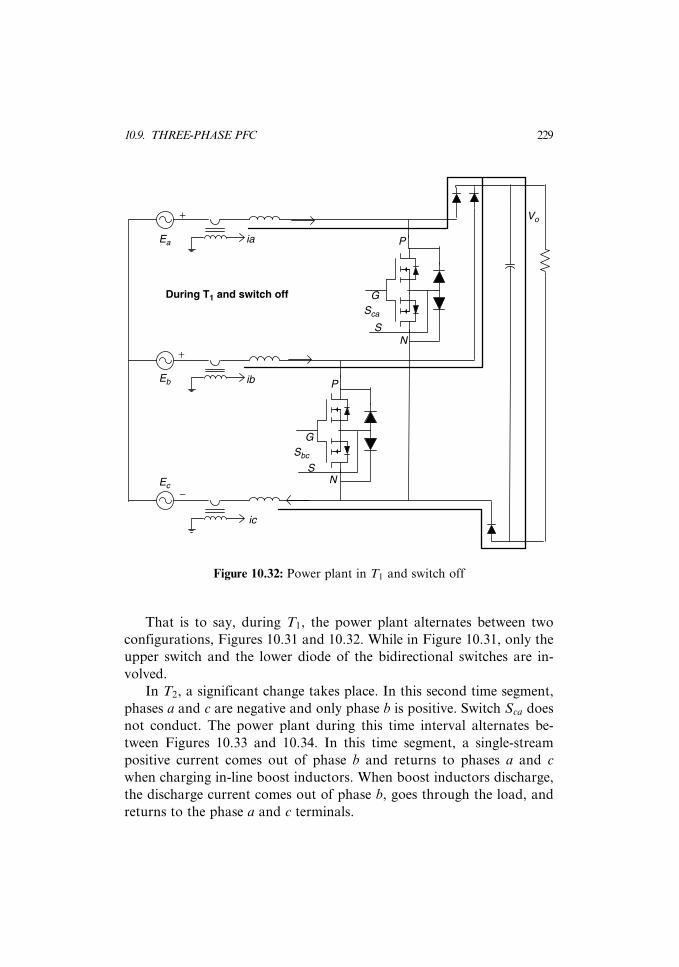
That is to say, during T1, the power plant alternates between two
configurations, Figures 10.31 and 10.32. While in Figure 10.31, only the
upper switch and the lower diode of the bidirectional switches are in-
volved.
In T2, a significant change takes place. In this second time segment,
phases a and c are negative and only phase b is positive. Switch Sca does
not conduct. The power plant during this time interval alternates be-
tween Figures 10.33 and 10.34. In this time segment, a single-stream
positive current comes out of phase b and returns to phases a and c
when charging in-line boost inductors. When boost inductors discharge,
the discharge current comes out of phase b, goes through the load, and
returns to the phase a and c terminals.
Ea
Eb
Ec
Vo
Sbc
P
N
Sca
P
N
ia
ic
ib
G
G
S
S
During T1 and switch off
+
+
−
Figure 10.32: Power plant in T1 and switch off
10.9. THREE-PHASE PFC 229

Ea
Eb
Ec
Vo
Sab
P
N
Sbc
P
N
ia
ic
ib
G
G
S
S
During T2 and switch on
+
−
−
Figure 10.33: Power plant in T2, switch on and charging
Ea
Eb
Ec
Vo
Sab
P
N
Sbc
P
N
ia
ic
ib
G
G
S
S
During T2 and switch off
+
−
−
Figure 10.34: Power plant in T2, switch off and discharging
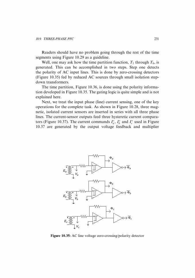
Readers should have no problem going through the rest of the time
segments using Figure 10.29 as a guideline.
Well, one may ask how the time partition function, T1 through T6, is
generated. This can be accomplished in two steps. Step one detects
the polarity of AC input lines. This is done by zero-crossing detectors
(Figure 10.35) fed by reduced AC sources through small isolation step-
down transformers.
The time partition, Figure 10.36, is done using the polarity informa-
tion developed in Figure 10.35. The gating logic is quite simple and is not
explained here.
Next, we treat the input phase (line) current sensing, one of the key
operations for the complete task. As shown in Figure 10.28, three mag-
netic, isolated current sensors are inserted in series with all three phase
lines. The current-sensor outputs feed three hysteretic current compara-
tors (Figure 10.37). The current commands I�a , I�b and I�c used in Figure
10.37 are generated by the output voltage feedback and multiplier
Ea
+
−
Φa
Φa
Va
Eb
Φb
Φb
Vb
Ec
Φc
Φc
Vc
+
−
+
−
Figure 10.35: AC line voltage zero-crossing/polarity detector
10.9. THREE-PHASE PFC 231
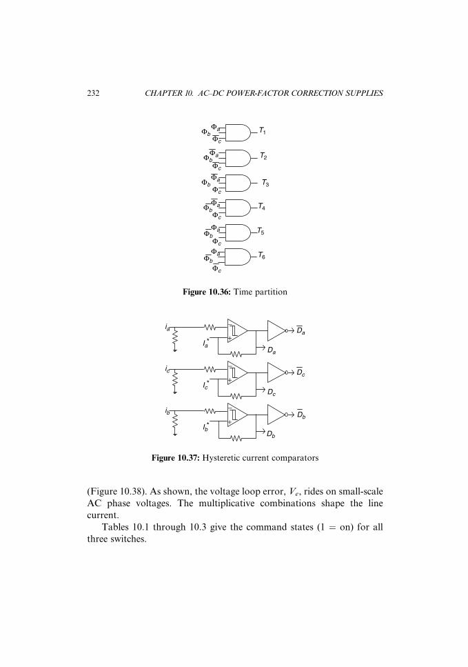
(Figure 10.38). As shown, the voltage loop error, Ve, rides on small-scale
AC phase voltages. The multiplicative combinations shape the line
current.
Tables 10.1 through 10.3 give the command states (1 ¼ on) for all
three switches.
ΦaΦb
Φa
Φc
ΦaΦbΦc
ΦaΦbΦc
ΦaΦbΦc
ΦaΦb
Φc
ΦbΦc
T1
T2
T3
T4
T5
T6
Figure 10.36: Time partition
+
−ia
Ia*Da
Da
+
−ic
Ic*Dc
Dc
+
−ib
Ib*Db
Db
Figure 10.37: Hysteretic current comparators
232 CHAPTER 10. AC–DC POWER-FACTOR CORRECTION SUPPLIES
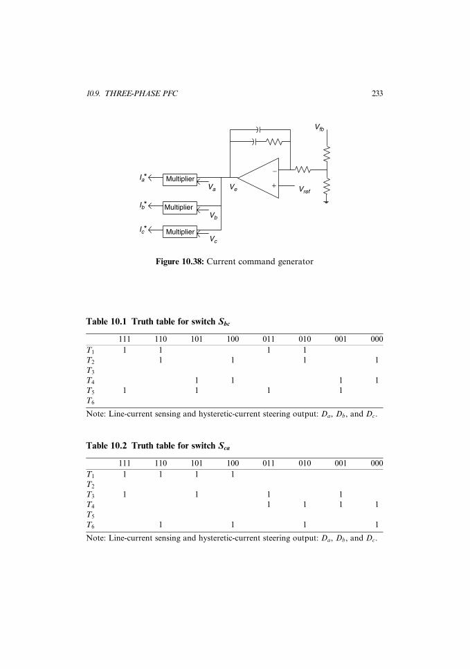
+
−
VrefVe
Multiplier
Multiplier
MultiplierVc
Vb
Va
Ia*
Ib*
Ic*
Vfb
Figure 10.38: Current command generator
Table 10.1 Truth table for switch Sbc
111 110 101 100 011 010 001 000
T1 1 1 1 1
T2 1 1 1 1
T3
T4 1 1 1 1
T5 1 1 1 1
T6
Note: Line-current sensing and hysteretic-current steering output: Da, Db, and Dc.
Table 10.2 Truth table for switch Sca
111 110 101 100 011 010 001 000
T1 1 1 1 1
T2
T3 1 1 1 1
T4 1 1 1 1
T5
T6 1 1 1 1
Note: Line-current sensing and hysteretic-current steering output: Da, Db, and Dc.
10.9. THREE-PHASE PFC 233

From Table 10.1 and employing Boolean algebra, for instance, in the
first row corresponding to T1, the decision logic for turning on switch Sbc
can be expressed as
T1(DaDbDc þDaDbDc þDaDbDc þDaDbDc)
¼ T1(DaDb þDaDb) ¼ T1Db (10:34)
Following the same procedure for the rest, the overall switch logic is, for
Sbc,
Sbc ¼ T1Db þ T2Dc þ T4Db þ T5Dc (10:35)
for Sca,
Sca ¼ T1Da þ T3Dc þ T4Da þ T6Dc (10:36)
and for Sab,
Sab ¼ T2Da þ T3Db þ T5Da þ T6Db (10:37)
The preceding logic is implemented with switch steering logic (Figure
10.39) including isolation.
At this point, we can certainly assemble all the preceding in a single
figure, as in Figure 10.40, that shows the complete circuit in a block
diagram form with key variables passed along from one block to another.
Further improvement is possible by considering current advancement
in digital signal processing. It looks like at least Figures 10.38 and 10.39
Table 10.3 Truth table for switch Sab
111 110 101 100 011 010 001 000
T1
T2 1 1 1 1
T3 1 1 1 1
T4
T5 1 1 1 1
T6 1 1 1 1
Note: Line-current sensing and hysteretic-current steering output: Da, Db, and Dc.
234 CHAPTER 10. AC–DC POWER-FACTOR CORRECTION SUPPLIES

Opto
T1
T3
T4
T6
Da
Dc
Da
Dc
Sca
Da
Da
Opto
T2
T3
T5
T6
Db
Db
Sab
Sbc
T1
T2
T4
T5
Db
Db
Dc
Dc
Opto
Figure 10.39: Switch steering logic with isolation.
Power stage, Figure 10.28
Current commandgenerator
Figure 10.38
Time segmentationFigures 10.35,10.36
Switch-steeringlogic, Figure 10.39
Line-current sensingand hysteretic currentsteering, Figure 10.37
3-phase input
Line current
6 lines
6 lines
Vout
ia, ib ,ic
Ea , E
b , Ec
T1. . . T
6Va,Vb,Vc
Ia *, Ib *, Ic *
Da, Db, Dcetc.
Da,Db,Dc.etc
ia, ib ,ic
T1. . .T6
Va,Vb,Vc
Sab, Sbc, Sca
Figure 10.40: Complete three-phase PFC

can be replaced by a field programmable gate array. This action may
simplify Figure 10.40 to Figure 10.41. Of course, note that many digital-
to-analog or analog-to-digital interfaces are not shown but implied in the
last figure.
Power stage, Figure10.28
Time segmentationFigures 10.35,10.36
Line-current sensingand hysteretic-currentsteering, Figure 10.37
3-phase input
Line current
6 lines
6 lines
Vout
ia, ib, ic
Ea , E
b , Ec
T1. . . T
6
Va,Vb,Vc
Ia*, Ib
*, Ic* Va, Vb, Vc
Da, Db, Dc.etc
Da, Db, Dcetc.
ia, ib, ic
T1. . .T6
Sab, Sbc, Sca
Gate array, mixed signal
Figure 10.41: Complete three-phase PFC using gate array
236 CHAPTER 10. AC–DC POWER-FACTOR CORRECTION SUPPLIES
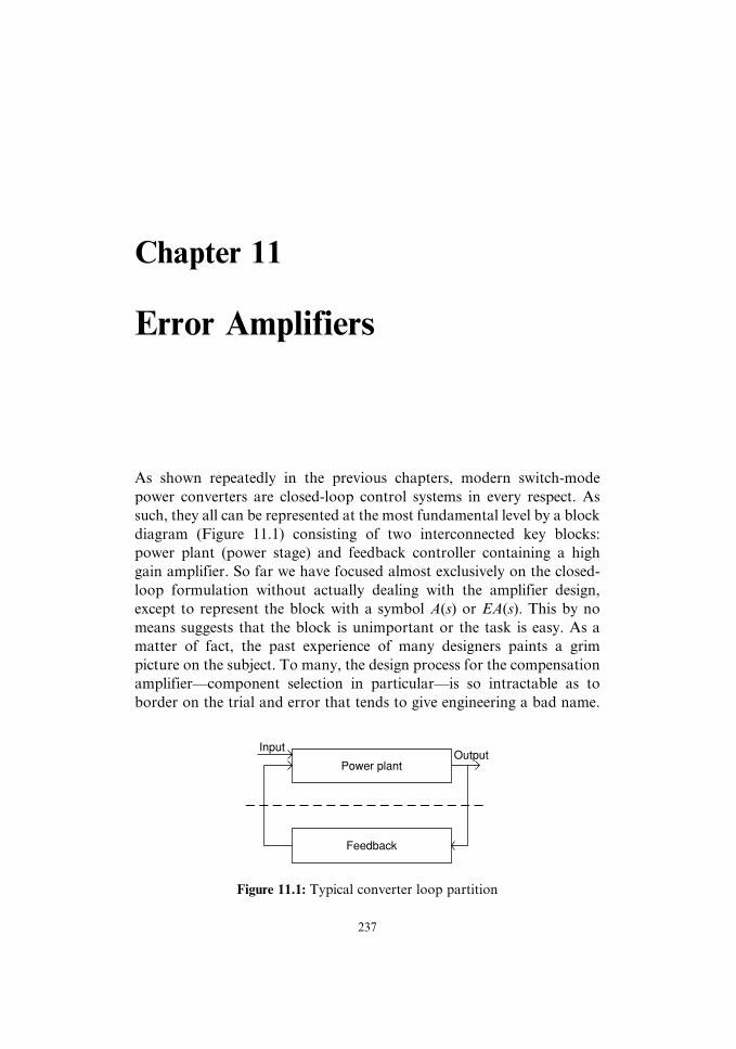
Chapter 11
Error Amplifiers
As shown repeatedly in the previous chapters, modern switch-mode
power converters are closed-loop control systems in every respect. As
such, they all can be represented at the most fundamental level by a block
diagram (Figure 11.1) consisting of two interconnected key blocks:
power plant (power stage) and feedback controller containing a high
gain amplifier. So far we have focused almost exclusively on the closed-
loop formulation without actually dealing with the amplifier design,
except to represent the block with a symbol A(s) or EA(s). This by no
means suggests that the block is unimportant or the task is easy. As a
matter of fact, the past experience of many designers paints a grim
picture on the subject. To many, the design process for the compensation
amplifier—component selection in particular—is so intractable as to
border on the trial and error that tends to give engineering a bad name.
237
Power plant
Feedback
InputOutput
Figure 11.1: Typical converter loop partition
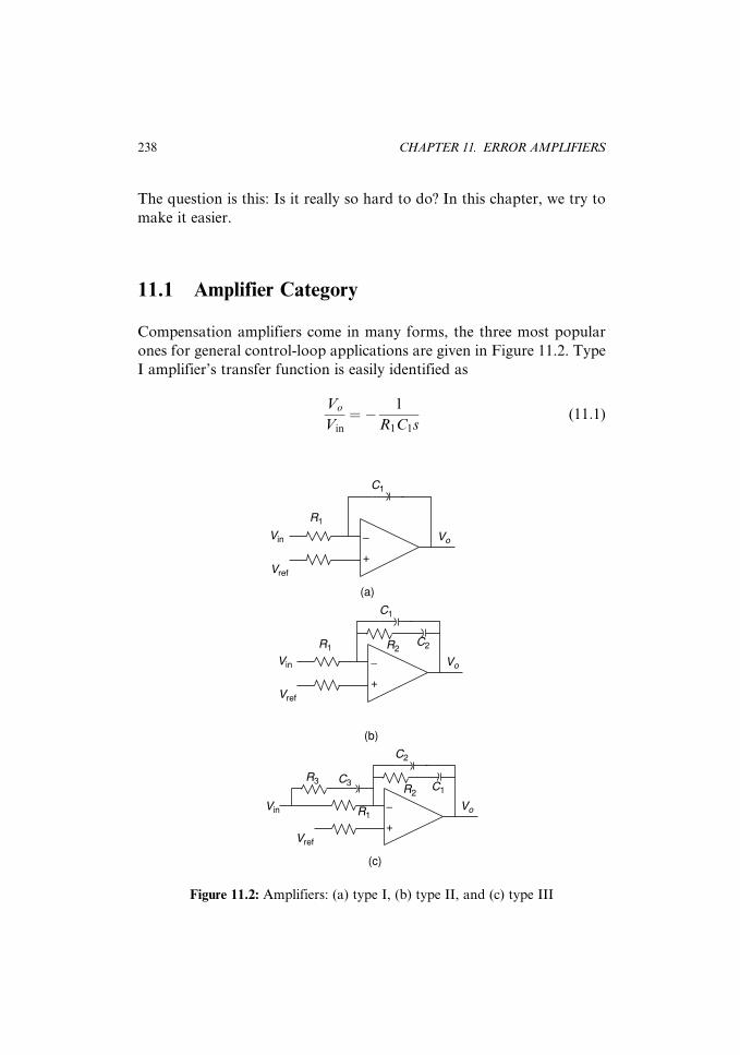
The question is this: Is it really so hard to do? In this chapter, we try to
make it easier.
11.1 Amplifier Category
Compensation amplifiers come in many forms, the three most popular
ones for general control-loop applications are given in Figure 11.2. Type
I amplifier’s transfer function is easily identified as
Vo
Vin
¼ � 1
R1C1s(11:1)
+
−
C1
C1
C1
C2
C2
C3R3
R2
R1
R2
R1
R1
Vo
Vo
Vo
Vin
Vin
Vin
Vref
Vref
Vref
(a)
+
−
(b)
+
−
(c)
Figure 11.2: Amplifiers: (a) type I, (b) type II, and (c) type III
238 CHAPTER 11. ERROR AMPLIFIERS

The amplifier gives a �20dB/decade roll-off starting at zero frequency
and a constant �2708, or 908, phase. Type II amplifier’s transfer function
is given as
Vo
Vin
¼ � R2 . C2 . sþ 1
R1(C1 þ C2)s R2 .C1 .C2
C1 þ C2
. sþ 1
� � (11:2)
The type II amplifier gives three frequency points of importance. If
standing alone, the pole at zero frequency crosses the zero dB axis at fp0,
while the pole–zero pair offers corner frequencies, fp1 and fz1, respec-
tively. The three frequencies are given as
fp0 ¼1
2 . p .R1(C1 þ C2)
fp1 ¼1
2 . p .R2 .C1 . C2
C1 þ C2
fz1 ¼1
2 . p .R2 . C2
(11:3)
Important behaviors begin to show up for the type II amplifier (Figure
11.3). Instead of being a constant, the amplifier’s phase changes, in our
favor, between the pole–zero pair’s frequencies. The phase still starts from
�2708 at low frequency, but it moves toward�1808 between fp1 and fz1. In
other words, a phase boost takes place (see Wu [10]). The amount of boost
is a function of the separation of pole–zero pair frequencies. If a fre-
quency, fc, is picked such that fz1 < fc < fp1, fc=fz1 ¼ k, and fc=fp1 ¼ 1=k,
the amount of phase boost at the selected frequency is
ab ¼ 2 . tan�1 k� p
2(11:4)
Or, the pole–zero separation, fp1=fz1 ¼ k2, satisfies
k2 ¼ tanab
2þ p
4
� �h i2, ab in radians
¼ tanab
2þ 45
� � p
180
h in o2
, ab in degrees (11:5)
11.1. AMPLIFIER CATEGORY 239

10 102 104103
Frequency
Frequency
dB
dB
20
40
fz1
fz1 fp1 fp0fc
fp1
fp0
(a)
20
40
GA
G − A
(b)
Figure 11.3: Type II amplifier gain
This equation shows that, to recover about 808, k2 equals about 130.
That is, the pole–zero pair is separated by slightly more than two decades
in frequency.
For the type III amplifier, we can follow a similar procedure. The
transfer function is given as
Vo
Vin
¼ � (R2 .C1 . sþ 1)[(R1 þ R3)C3 . sþ 1]
R1(C1 þ C2)s R2 .C1 . C2
C1 þ C2
. sþ 1
� �(R3 . C3 . sþ 1)
(11:6)
Consequently, five frequencies are involved—fp0, fp1, fz1, fp2, and fz2:
fp0 ¼1
2 . p . R1(C1 þ C2)
fp1 ¼1
2 . p . R2 .C1 . C2
C1 þ C2
fp2 ¼1
2 . p . R3 .C3
fz1 ¼1
2 . p . R2C1
fz2 ¼1
2 . p . (R1 þ R3) . C3
(11:7)
240 CHAPTER 11. ERROR AMPLIFIERS

Frequency
Frequency
dB
dB
20
40
(a)
20
40 G
kG − 20 ⋅ log
k20 ⋅ log
(b)
10 102 104103fz1
fz1 fc
fp1
fp1 fp0
Figure 11.4: Type III amplifier gain
In practical application, it is advantageous to make fp1 ¼ fp2 and
fz1 ¼ fz2. In effect, a double pole and a double zero are created (Figure
11.4). The phase still starts from �2708 at low frequency, but it moves
toward �908 between fp1 and fz1, see Wu [10]. In other words, a greater
phase boost takes place with type III. The amount of boost is again a
function of the separation of pole–zero pair frequencies. If a frequency,
fc, is picked such that fz1 < fc < fp1, fc=fz1 ¼ffiffiffikp
, and fc=fp1 ¼ 1=ffiffiffikp
, the
amount of phase boost at the selected frequency is
ab ¼ 2 . tan�1ffiffiffikp� p
2(11:8)
Or, the pole–zero separation, fp1=fz1 ¼ k, is
k ¼ tanab
2þ p
4
� �h i2, ab in radians
¼ tanab
2þ 45
� � p
180
h in o2
, ab in degrees (11:9)
This equation shows that, to recover about 1608, k equals about 110.
That is, the double pole–zero is separated by slightly more than two
decades in frequency.
11.1. AMPLIFIER CATEGORY 241
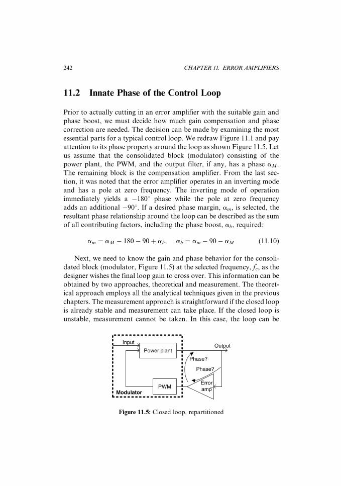
11.2 Innate Phase of the Control Loop
Prior to actually cutting in an error amplifier with the suitable gain and
phase boost, we must decide how much gain compensation and phase
correction are needed. The decision can be made by examining the most
essential parts for a typical control loop. We redraw Figure 11.1 and pay
attention to its phase property around the loop as shown Figure 11.5. Let
us assume that the consolidated block (modulator) consisting of the
power plant, the PWM, and the output filter, if any, has a phase aM .
The remaining block is the compensation amplifier. From the last sec-
tion, it was noted that the error amplifier operates in an inverting mode
and has a pole at zero frequency. The inverting mode of operation
immediately yields a �1808 phase while the pole at zero frequency
adds an additional �908. If a desired phase margin, am, is selected, the
resultant phase relationship around the loop can be described as the sum
of all contributing factors, including the phase boost, ab, required:
am ¼ aM � 180� 90þ ab, ab ¼ am � 90� aM (11:10)
Next, we need to know the gain and phase behavior for the consoli-
dated block (modulator, Figure 11.5) at the selected frequency, fc, as the
designer wishes the final loop gain to cross over. This information can be
obtained by two approaches, theoretical and measurement. The theoret-
ical approach employs all the analytical techniques given in the previous
chapters. The measurement approach is straightforward if the closed loop
is already stable and measurement can take place. If the closed loop is
unstable, measurement cannot be taken. In this case, the loop can be
Power plant
PWM
InputOutput
−Erroramp
Modulator
Phase?
Phase?
Figure 11.5: Closed loop, repartitioned
242 CHAPTER 11. ERROR AMPLIFIERS
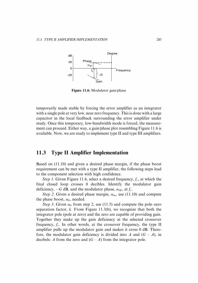
temporarily made stable by forcing the error amplifier as an integrator
with a single pole at very low, near zero frequency. This is done with a large
capacitor in the local feedback surrounding the error amplifier under
study. Once this temporary, low-bandwidth mode is forced, the measure-
ment can proceed. Either way, a gain/phase plot resembling Figure 11.6 is
available. Now, we are ready to implement type II and type III amplifiers.
11.3 Type II Amplifier Implementation
Based on (11.10) and given a desired phase margin, if the phase boost
requirement can be met with a type II amplifier, the following steps lead
to the component selection with high confidence.
Step 1. Given Figure 11.6, select a desired frequency, fc, at which the
final closed loop crosses 0 decibles. Identify the modulator gain
deficiency, �G dB, and the modulator phase, aM , at fc.
Step 2. Given a desired phase margin, am, use (11.10) and compute
the phase boost, ab, needed.
Step 3. Given ab from step 2, use (11.5) and compute the pole–zero
separation factor, k. From Figure 11.3(b), we recognize that both the
integrator pole (pole at zero) and the zero are capable of providing gain.
Together they make up the gain deficiency at the selected crossover
frequency, fc. In other words, at the crossover frequency, the type II
amplifier pulls up the modulator gain and makes it cross 0 dB. There-
fore, the modulator gain deficiency is divided into A and (G – A), in
decibels: A from the zero and (G – A) from the integrator pole.
Frequency
dB
0
20
fc−20
Phase
−G
Degree
Gain
αM
Figure 11.6: Modulator gain/phase
11.3. TYPE II AMPLIFIER IMPLEMENTATION 243

Step 4. Since Figure 11.3 is in log-scale, the following can be estab-
lished for fz1:
20 . logfc
fc=k
� �¼ 20 . log (k) ¼ A (11:11)
Step 5. Similarly, the following holds for fpo, the integrator:
20 . logfp0
fc
� �¼ G� A ¼ G� 20 . log (k)
fp0 ¼ 10[G20�log (k)] . fc
(11:12)
Step 6. Rewrite (11.3) as
fz1 ¼1
2 . p . R2 . C2
¼ fc
k(11:13)
fp1 ¼1
2 . p . R2 .C1 .C2
C1 þ C2
¼ k . fc (11:14)
fp0 ¼1
2 . p . R1(C1 þ C2)¼ 10[
G20�log (k)] . fc (11:15)
Step 7. Take the ratio of (11.13) to (11.14). C2 is expressed in terms of
C1. Consequently, (C1 þ C2) is also expressed in terms of C1:
C2 ¼ (k2 � 1)C1, C1 þ C2 ¼ k2C1 (11:16)
In general, R1 is preselected for bias current and offset voltage consider-
ations.
Step 8. Plug in the second part of (11.16) in (11.15) and we have the
following:
C1 ¼1
2 . p . R1 . k2 . fc .10G20�log (k)
� � (11:17)
244 CHAPTER 11. ERROR AMPLIFIERS

Step 9. Then, C2 follows from the first part of (11.16).
Step 10. Use (11.13) and calculate the last part R2:
R2 ¼1
2 . p .fc
k. C2
(11:18)
11.4 Type III Amplifier Implementation
Based on (11.10) and given a desired phase margin, if the phase boost
requirement can be met with a type III amplifier, the following steps lead
to the component selection with high confidence.
Step 1. Given Figure 11.6, select a desired frequency, fc, at which the
final closed loop crosses 0 dB. Identify the modulator gain deficiency, –G
dB, and the modulator phase, aM , at fc.
Step 2. Given a desired phase margin, am, use (11.10) and compute
the phase boost, ab, needed.
Step 3. Given ab from step 2, use (11.9) and compute the pole–zero
separation factor, k. From Figure 11.4(b), we recognize that both the
integrator pole (pole at zero) and the double zero are capable of gain
contribution. Together they make up the gain deficiency at the selected
crossover frequency, fc.
Step 4. Since Figure 11.4 is in log scale, the following can be estab-
lished for fz1:
20 . logfc
fc=ffiffiffikp
!¼ 20 . log
ffiffiffikp
(11:19)
Step 5. Similarly, the following holds for fpo, the integrator:
20 . logfp0
fc=ffiffiffikp
!¼ G� 20 . log
ffiffiffikp¼ G� 10 . log k
fp0 ¼ 10G�10 . log k
20 .fcffiffiffikp
(11:20)
11.4. TYPE III AMPLIFIER IMPLEMENTATION 245

Step 6. Rewrite (11.7) as
fp0 ¼1
2 . p . R1(C1 þ C2)¼ 10
G�10 . log k20 .
fcffiffiffikp
fp1 ¼1
2 . p .R2 .C1 . C2
C1 þ C2
¼ffiffiffikp
. fc
fp2 ¼1
2 . p .R3 . C3
¼ fp1 (11:21)
fz1 ¼1
2 . p .R2C1
¼ fcffiffiffikp
fz2 ¼1
2 . p . (R1 þ R3) . C3
¼ fz1
Step 7. Take the ratio of fp1 to fz1. C1 is expressed in terms of C2.
Consequently (C1 þ C2) is also expressed in terms of C2:
C1 ¼ (k� 1)C2, C1 þ C2 ¼ k . C2 (11:22)
In general, R1 is preselected for bias current and offset voltage consider-
ations.
Step 8. Plug in the second part of (11.22) in fp0 of (11.21) and we have
the following:
C2 ¼1
2 . p . R1 .ffiffiffikp
. 10G�10 . log k
20
(11:23)
Step 9. Then, C1 follows from the first part of (11.22).
Step 10. With C1 from step 9, use the fz1 equation in (11.21) to
calculate R2:
R2 ¼ffiffiffikp
2 . p . fc .C1
(11:24)
Step 11. Take the ratio of fp2 to fz2; R3 is expressed in terms of R1:
246 CHAPTER 11. ERROR AMPLIFIERS

R3 ¼R1
k� 1(11:25)
Step 12. The last part is
C3 ¼1
2 . p .R3 .ffiffiffikp
. fc(11:26)
11.5 Example for Type II Amplifier Implementation
In Chapter 13, a Cuk converter (Figure 13.1) gives a closed-loop band-
width of only about 3 KHz (Figures 13.7 and 13.8). Following the steps
given in Section 11.3, the type II error amplifier is improved with new
values, R323 ¼ 23K, C311 ¼ 1:9 nF, C313 ¼ 290 pF. Figure 11.7 shows
that the bandwidth is extended to 5 KHz without phase margin or gain
margin degradation.
11.5. EXAMPLE FOR TYPE II AMPLIFIER IMPLEMENTATION 247

TdB(n)
100 K10 f(n)10 100 1•103 1•104 1•105
100 K10 f(n)10 100 1•103 1•104 1•105
−80−80
−60
−40
−20
0
20
40
6060
θ(n)
−180−180
−120
−60
0
60
120
180180
10 100 1K 10K 100KSTART 10 . 000Hz STOP 100 000 . 00Hz
REF LEVEL0. 000dB0 . 0deg
/DIV10 . 000dB45 . 000deg
MARKER 5 141 . 642HzMAG (A/R) 0 . 095dBMARKER 5 141 . 642HzPHASE (A/R) 57 . 971deg
C
Figure 11.7: Improved loop gain for a Cuk converter
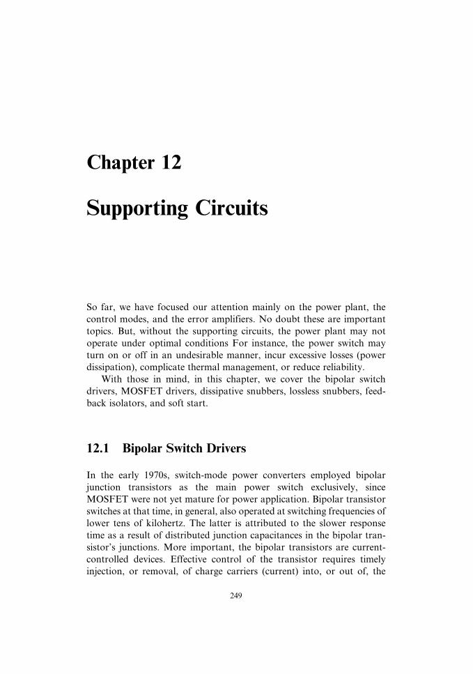
Chapter 12
Supporting Circuits
So far, we have focused our attention mainly on the power plant, the
control modes, and the error amplifiers. No doubt these are important
topics. But, without the supporting circuits, the power plant may not
operate under optimal conditions For instance, the power switch may
turn on or off in an undesirable manner, incur excessive losses (power
dissipation), complicate thermal management, or reduce reliability.
With those in mind, in this chapter, we cover the bipolar switch
drivers, MOSFET drivers, dissipative snubbers, lossless snubbers, feed-
back isolators, and soft start.
12.1 Bipolar Switch Drivers
In the early 1970s, switch-mode power converters employed bipolar
junction transistors as the main power switch exclusively, since
MOSFET were not yet mature for power application. Bipolar transistor
switches at that time, in general, also operated at switching frequencies of
lower tens of kilohertz. The latter is attributed to the slower response
time as a result of distributed junction capacitances in the bipolar tran-
sistor’s junctions. More important, the bipolar transistors are current-
controlled devices. Effective control of the transistor requires timely
injection, or removal, of charge carriers (current) into, or out of, the
249
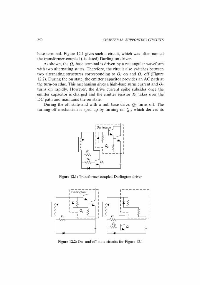
base terminal. Figure 12.1 gives such a circuit, which was often named
the transformer-coupled (-isolated) Darlington driver.
As shown, the Q2 base terminal is driven by a rectangular waveform
with two alternating states. Therefore, the circuit also switches between
two alternating structures corresponding to Q2 on and Q2 off (Figure
12.2). During the on state, the emitter capacitor provides an AC path at
the turn-on edge. This mechanism gives a high-base surge current and Q2
turns on rapidly. However, the drive current spike subsides once the
emitter capacitor is charged and the emitter resistor R1 takes over the
DC path and maintains the on state.
During the off state and with a null base drive, Q2 turns off. The
turning-off mechanism is sped up by turning on Q1, which derives its
Darlington
R1
R2
Q2
Q1
Figure 12.1: Transformer-coupled Darlington driver
Darlington
R1
Q2
R1
R2Q1
Figure 12.2: On- and off-state circuits for Figure 12.1
250 CHAPTER 12. SUPPORTING CIRCUITS
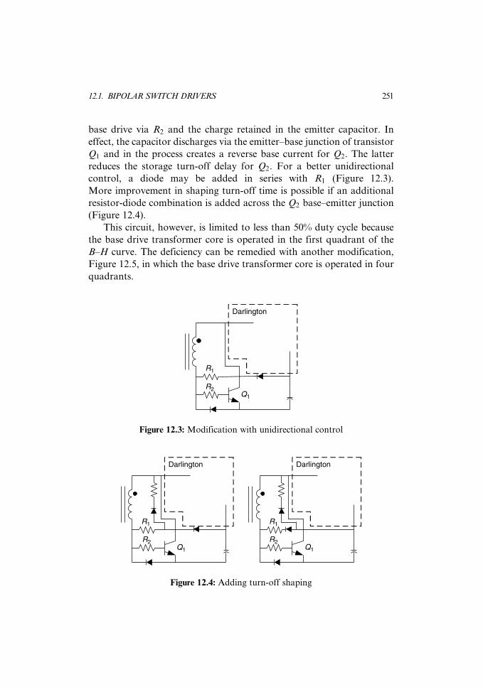
base drive via R2 and the charge retained in the emitter capacitor. In
effect, the capacitor discharges via the emitter–base junction of transistor
Q1 and in the process creates a reverse base current for Q2. The latter
reduces the storage turn-off delay for Q2. For a better unidirectional
control, a diode may be added in series with R1 (Figure 12.3).
More improvement in shaping turn-off time is possible if an additional
resistor-diode combination is added across the Q2 base–emitter junction
(Figure 12.4).
This circuit, however, is limited to less than 50% duty cycle because
the base drive transformer core is operated in the first quadrant of the
B–H curve. The deficiency can be remedied with another modification,
Figure 12.5, in which the base drive transformer core is operated in four
quadrants.
Q1
R1
R2
Darlington
Figure 12.3: Modification with unidirectional control
Darlington
Q1Q1
R1R1
R2R2
Darlington
Figure 12.4: Adding turn-off shaping
12.1. BIPOLAR SWITCH DRIVERS 251
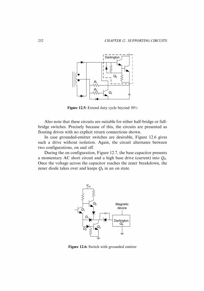
Also note that these circuits are suitable for either half-bridge or full-
bridge switches. Precisely because of this, the circuits are presented as
floating drives with no explicit return connections shown.
In case grounded-emitter switches are desirable, Figure 12.6 gives
such a drive without isolation. Again, the circuit alternates between
two configurations, on and off.
During the on configuration, Figure 12.7, the base capacitor presents
a momentary AC short circuit and a high base drive (current) into Q4.
Once the voltage across the capacitor reaches the zener breakdown, the
zener diode takes over and keeps Q4 in an on state.
Darlington
Q2
Q1
R1
R2
Figure 12.5: Extend duty cycle beyond 50%
Vcc
Darlington
Magneticdevice
Q4Q3
Q1
D1
D2
Q2
Figure 12.6: Switch with grounded emitter
252 CHAPTER 12. SUPPORTING CIRCUITS
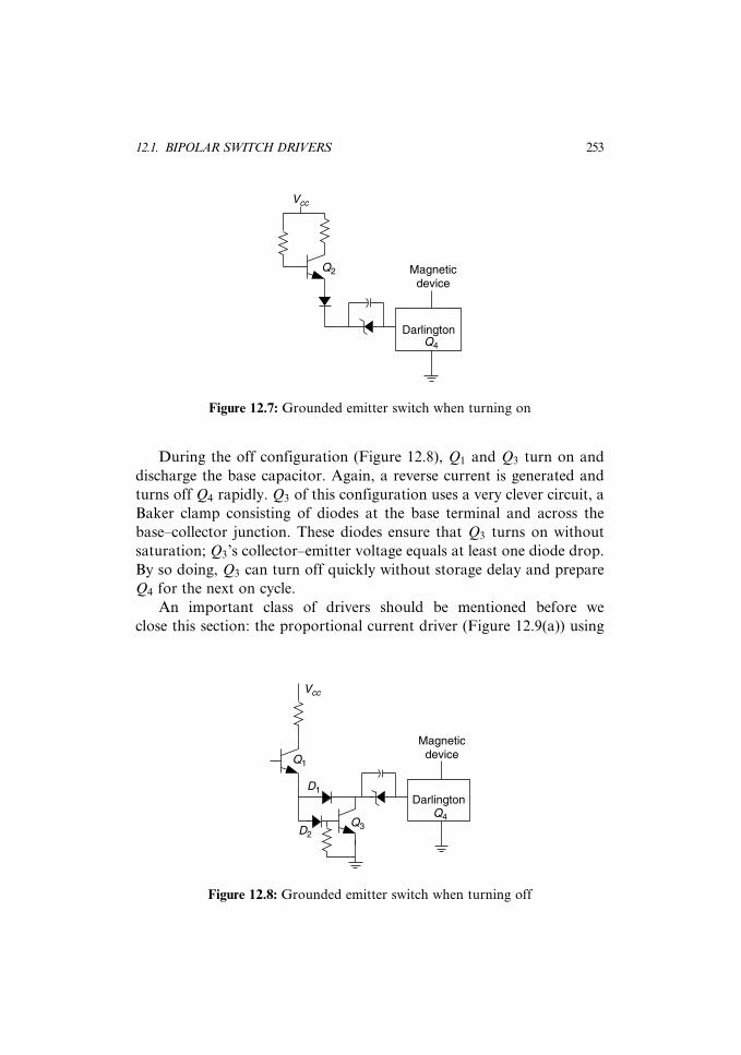
During the off configuration (Figure 12.8), Q1 and Q3 turn on and
discharge the base capacitor. Again, a reverse current is generated and
turns off Q4 rapidly. Q3 of this configuration uses a very clever circuit, a
Baker clamp consisting of diodes at the base terminal and across the
base–collector junction. These diodes ensure that Q3 turns on without
saturation; Q3’s collector–emitter voltage equals at least one diode drop.
By so doing, Q3 can turn off quickly without storage delay and prepare
Q4 for the next on cycle.
An important class of drivers should be mentioned before we
close this section: the proportional current driver (Figure 12.9(a)) using
Darlington
Magneticdevice
Vcc
Q4
Q2
Figure 12.7: Grounded emitter switch when turning on
Darlington
Magneticdevice
Vcc
Q4Q3
Q1
D1
D2
Figure 12.8: Grounded emitter switch when turning off
12.1. BIPOLAR SWITCH DRIVERS 253

a current transformer. Like the drivers given previously, this driver
operates in two distinctive configurations (Figure 12.9(b) and (c)). In
the (Q2) on state, the Darlington transistor base drive current is propor-
tional to the collector current via the turn ratio, IB ¼ (N78=N56)IC , and
an important constraint is also imposed: the on-time is limited to
N78
N56
þ 1
� �(VBE þ Vz)ton # 2 . ls (12:1)
If N78 is chosen, one turn and given a selected transformer core with
known saturation flux, ls, and a desired on time, ton, (12.1) gives N56. The
lower bound of the off-time, toff , can be approximated with ls=Vs. The
values of ton and toff together give some indication of switching frequency.
However, if the switching frequency is fixed and selected, either the on-
time or the off-time becomes a variable subjected to closed-loop control.
Vcc
VccVcc
Darlington
Vin
VinVin
N78
N78N78
N56N12Q1
Q2
Q2
N34
N34N34
(a)
Darlington
N12 N12N56 N56
Darlington
(b) (c)
Figure 12.9: Proportional drives
254 CHAPTER 12. SUPPORTING CIRCUITS

One unique feature of the transformer is that the core is intentionally
driven to saturation during the off time when Q1 is on. However, it is not
saturated when driven for the on state. In other words, the core is
operated in four quadrants but skewed to one end of magnetic core
saturation. Also keep in mind that the Darlington driver operates in an
on/off switch mode instead of a linear mode. When in the on-state, the
concept of current gain is murky. This makes the selection of ratio
N78=N56 and the circuit design a whole lot less straightforward.
12.2 MOSFET Switch Drivers
In contrast to the bipolar devices, the MOSFETs are voltage-controlled
devices. Insofar as controlling the switch on/off state, the gate voltage
control for MOSFET resembles to some extent the base current control
for bipolar transistors. As a matter of fact, to achieve switch on/off for
MOSFET at high speed, drivers with high forward and reverse current
capability are often employed. In this section, we present several circuits
for that purpose without any in-depth analysis. Readers can refer to Wu
[10] for the relevant discussions.
For an N-channel MOSFET, Figure 12.10 is the simplest driver. The
upper bipolar transistor is responsible for turning on while the lower is
for turning off. By introducing a capacitor, Figure 12.11, a capacitor-
coupled driver similar to Figure 12.6 is created. The improved version
offers a higher, positive on-surge current charging the built-in gate-
to-source capacitance when turning on. When turning off, the coupling
capacitor and the lower driver provide a transitory negative voltage at
the MOSFET gate. It is also possible to split the gate resistor, Figure
12.12. The circuit gives designer more degrees of freedom.
More shaping for the gate drive can be done by introducing a diode,
Figure 12.13, which gives two different on/off drive-time constants. With a
transformer incorporated, a floating drive is also feasible, Figure 12.14.
Withtransformercoupling, isolation isalsoachieved.Withoutdoubt, those
series of modifications show the power and the beauty of analog design.
For the P-channel MOSFET used as power switches, Figure 12.15
gives the simplest version. Switching on and off the bipolar driver turns
the P-channel on and off, too.
12.2. MOSFET SWITCH DRIVERS 255

Vcc
Vin
Figure 12.10: Nonisolated N-channel MOSFET driver
Vcc
Vin
Figure 12.11: Capacitor coupled N-channel MOSFET driver
Vcc
Vin
Figure 12.12: Modified capacitor coupled N-channel MOSFET driver
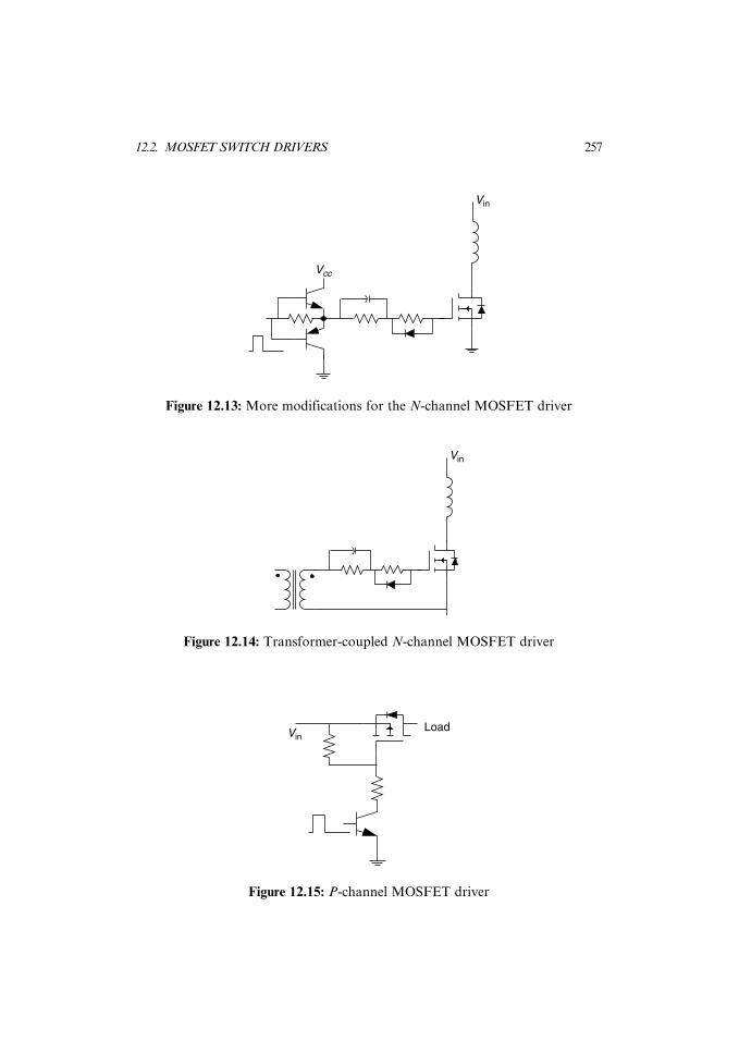
Vcc
Vin
Figure 12.13: More modifications for the N-channel MOSFET driver
Vin
Figure 12.14: Transformer-coupled N-channel MOSFET driver
VinLoad
Figure 12.15: P-channel MOSFET driver
12.2. MOSFET SWITCH DRIVERS 257

Surge suppression may be included if a capacitor is added across the
gate and source terminals (Figure 12.16). The transient property of
capacitor voltage makes the P-channel device behave like a variable
resistor during the turn-on phase. In case the input voltage varies over
a wide range, the driver network, as shown, may not work for low input.
Then Figure 12.17(a) provides a way out.
VinLoad
Figure 12.16: P-channel MOSFET switch with a soft-starting driver
Load
On
Off
VinVin
Vin
Load
On
Off
(a) (b)
Load
On
Off
(c)
Figure 12.17: P-channel MOSFET switch for variable input
258 CHAPTER 12. SUPPORTING CIRCUITS

The combination of a zener diode and a resistor take the input vari-
ation out of the picture and the driver is now capable of riding through a
low-input condition. Furthermore, a diode placed strategically as shown
in Figure 12.17(b) gives the circuit enhanced speed in switching.
12.3 Dissipative Snubber
The load lines encountered in a switch-mode power converter, in general,
are inductive. On the i–v coordinate plane, the power switch current and
voltage traverse a nonlinear trajectory. This load behavior exerts signifi-
cant stress on the switch in the form of local power dissipation that
elevates the device’s operating temperature and eventually reduces reli-
ability. The switch power dissipation can be roughly partitioned into two
parts: saturation losses and switching losses. The saturation losses are
attributed to the switch-on voltage and current and considered more of a
static nature, whereas the switching losses are associated more with the
transitory nature of rising and falling of switch voltage and current at the
very moment of on/off state changes. The latter, although dynamic in
nature, is more accessible to the designer and can be managed to some
extent. The voltage rising due to an inductive di/dt kickback is more
pronounced when the switch turns off. We, therefore, focus on the turn-
off snubbers, which are intended to manage the rate of falling current.
However, be cautioned that the process of snubber design is not easily
subjected to exact analysis. On the one hand, it treats circuits under
highly dynamic conditions in which stray elements involved in the pro-
cess are not totally accounted for. On the other hand, the parasitic
elements participating in the process are also nonlinear and the circuit
structure changes are not clearly tractable.
Conventional snubbers are made of passive elements. To direct cur-
rent flow in a preferred, guided way, diodes are also used. Figure 12.18(a)
gives a turn-off RC-diode snubber.
The operating sequence of the circuit can be briefly described as
follows. When the power switch terminates conduction, the inductive
load voltage flips polarity (Figure 12.18(b)). The clamping diode con-
ducts and keeps the magnetizing current flowing without interruption;
albeit at a decreasing rate. The action moves the energy previously
12.3. DISSIPATIVE SNUBBER 259

stored in the magnetic core to the capacitor. When the next on-cycle
commences, the clamping diode disengages the RC network and the
capacitor discharges its contents (Figure 12.18(c)). Readers are referred
to Wu [10] for a detailed mathematical analysis.
12.4 Lossless Snubber
It is clearly indicated in the previous section that the stored magnetic
energy is eventually dumped and dissipated in the resistive element. That
is the basis for calling the mechanism dissipative. A slight modification
alters the mechanism and makes it possible to recover some, if not all, of
the energy burned in the RC-diode clamping. Figure 12.19 shows the
general configuration of such a lossless snubber consisting of an LC-diode.
The key to the circuit operation is twofold. First, the stored (mag-
netizing) energy is transferred unidirectionally to the clamping capacitor
while the main switch is in the off-state (Figure 12.20(a)). When the main
switch turns on, the capacitor releases its contents to the clamping
inductor (Figure 12.20(b)).
The mathematics involved in the design of this type of snubber is not
as precise as we would like it to be. We do not attempt to cover it.
Readers interested in the topic may refer to Smith and Smedley [12] for
further studies.
Vin Vin Vin
+
_+
_
(a) (b) (c)
Figure 12.18: RC-diode turn-off snubber
260 CHAPTER 12. SUPPORTING CIRCUITS

12.5 Isolated Feedback
Both voltage and current feedbacks are used effectively in modern power
converters. Early on, voltage feedback had the upper hand, since it was
easy to implement. Nonisolated voltage feedback is even easier. It takes
just a node voltage and two resistors as a voltage divider. Of course, its
simplicity hides its shortcoming—no isolation. To implement isolated
voltage feedback, either magnetic or optical means must be employed.
The magnetic approach requires that the voltage being fed back must
Vin
Figure 12.19: LC-diode energy-recovering snubber
VinVin
+
+
_+
_
+
_
D2
La La
D1
D2
(a) (b )
Figure 12.20: Lossless snubber in (a) off and (b) on states
12.5. ISOLATED FEEDBACK 261

first be converted into AC form. The optical approach requires that the
feedback voltage be in current form to drive an optical element. You see,
the requirement of isolation wipes out the advantage voltage feedback
has over current feedback. The latter stands out as a better choice for
that reason and others. In addition to the ability of offering isolation,
current feedback can accommodate many auxiliary tasks: soft start,
current limiting, and current sharing, to name a few. Current feedback
is also less prone to noise. A voltage node with certain impedance can be
easily influenced by radiated emissions with no direct connection. In
contrast, it is not so easy to inject unwanted current into a current-
sensing branch without direct physical contact. It is with these under-
standings that Figure 12.21 is shown.
In the figure, the voltage feedback is converted into current. An
isolated magnetic current transformer with a ratio of 1:n takes the main
switch’s pulsating current and scales it by 1/n across the isolation barrier.
Both are summed, diodes D1 and D2, and injected across the current-
to-voltage conversion resistor, Rsen. Since Rsen has the lowest impedance,
T2
D2 D1
T2
Vcc
ReRb
Vin
Power plant and filter
+−
Vo
VrefErroramp
+
−PWMand
driver
v-feedback
i - feedack
Vref
RsenIsolatedsensing
Secondary
Primary
n
1
Nxy
ip
Figure 12.21: Isolated current feedback (U.S. patent 6,285,234)
262 CHAPTER 12. SUPPORTING CIRCUITS

the voltage of winding Nxy, where the current feedback and filter reside,
is slaved to that of winding n. In effect, the voltage of winding Nxy is
given by
Nxy.Rsen
n. hFE
VCC � VBE � A(Vref � Vo)
(1þ hFE)Re þ Rb
þ ip
n
� �(12:2)
Readers can refer to the patent for an alternative approach in which
current subtraction is implemented.
The opto-coupler is yet another device providing isolation. As shown
in Figure 12.22, the output to be regulated feeds a voltage divider—R1
and R2—that samples the output. The sampled output is compared with
a reference voltage, Vref¼2:5V, residing in TL431, a precision shunt regu-
lator. The error voltage is converted into drive current for the opto-
coupler, an LED and phototransistor combination. The current
transfer ratio (CTR) of the opto-coupler transfers the drive current.
The opto-coupler output current is converted into a feedback voltage
via a resistor.
12.6 Soft Start
Based on Figure 12.21, a soft-start mechanism can be easily implemented
by injecting a control current pulse at the current summing point of D1
and D2. The pulse current injector is just a current source with an RC
Vo
R3
R1
R2
Vcc
TL431
Opto
RefVfeedback
Figure 12.22: Optical isolator
12.6. SOFT START 263

timer (Figure 12.23). At the initial turn-on, the soft-start current forces a
high current across Rsen and develops a high voltage. The high voltage
forces the same across winding Nxy and in turn forces a minimum duty
cycle. The soft-start current diminishes gradually and normal function
takes over.
12.7 Negative-Charge Pump
Quite often, a negative supply at low current is needed for auxiliary
circuits. Figure 12.24(a) gives such a simple circuit.
When Q1 is turned off as in Figure 12.24(b), C1 is charged through D1
with the polarity shown. When Q1 is turned on, the contents of C1 are
reversed and transferred via D2 to C2. The off configuration gives two
equations:
R .C1
dv1
dtþ v1 ¼ Vs � Vcr, C2
dv2
dtþ v2
RL
¼ 0 (12:3)
T2
T2
Vcc
Vin
Power plant and filter
+
−
Vo
VrefErroramp
+
−PWMand
driver
v - feedback
i - feedback
Vref
RsenIsolatedsensing
Secondary
Primarysoftstart
1
n
Figure 12.23: Isolated current feedback with soft start
264 CHAPTER 12. SUPPORTING CIRCUITS
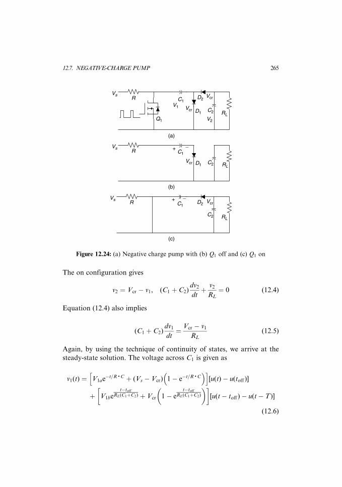
The on configuration gives
v2 ¼ Vcr � v1, (C1 þ C2)dv2
dtþ v2
RL
¼ 0 (12:4)
Equation (12.4) also implies
(C1 þ C2)dv1
dt¼ Vcr � v1
RL
(12:5)
Again, by using the technique of continuity of states, we arrive at the
steady-state solution. The voltage across C1 is given as
v1(t) ¼ V1ae�t=R . C þ (Vs � Vcr) 1� e�t=R . C
� �h i[u(t)� u(toff )]
þ V1bet�toff
RL(C1þC2) þ Vcr 1� et�toff
RL(C1þC2)
� �� �[u(t� toff )� u(t� T)]
(12:6)
RL
RL
Vcr
Vcr
D2
D1
C1
C1
RLQ1
R Vcr
Vcr
Vs
V1
V2
D2
D1
C1
C2
C2
C2
(a)
R
R
Vs
Vs
+_
(b)
+ _
(c)
Figure 12.24: (a) Negative charge pump with (b) Q1 off and (c) Q1 on
12.7. NEGATIVE-CHARGE PUMP 265

where
V1a ¼
�(Vs � Vcr) 1� etoff
R . C1
� ��1
�Vcr(1� eT�toff
RL(C1þC2)) eT�toff
RL(C1þC2)
��������
��������e
toff
R . C1 �1
�1 eT�toff
RL(C1þC2)
��������������
V1b ¼
etoff
R . C1 �(Vs � Vcr) 1� etoff
R . C1
� �
�1 �Vcr(1� eT�toff
RL(C1þC2))
��������
��������e
toff
R . C1 �1
�1 eT�toff
RL(C1þC2)
������������
(12:7)
The output voltage is given as
v2(t) ¼V2aet
RL. C2 [u(t)� u(toff )]
þ Vcr � V1bet�toff
RL(C1þC2) þ Vcr 1� et�toff
RL(C1þC2)
� �� ��
[u(t� toff )� u(t� T)] (12:8)
where
V2a ¼ Vcr � V1beT�toff
RL(C1þC2) þ Vcr 1� eT�toff
RL(C1þC2)
� �� �(12:9)
We give an example to illustrate and confirm the working of such a
circuit. Given R ¼ 30, C1 ¼ 10 mF, C2 ¼ 10 mF, RL ¼ 20, Vs ¼ 10 volts,
fs ¼ 100KHz, and toff ¼ 6 ms, the output voltage looks like Figure 12.25.
266 CHAPTER 12. SUPPORTING CIRCUITS

12.8 Single-Phase Full-Wave Rectifier with RC Filter
Both half-wave and full-wave rectifiers with RC filters have been in use
for years. The circuit given in Figure 12.26 has been known to exhibit
waveforms, as shown in Figure 12.27. However, as of this date (July
2004), no analytical solution in symbolic, closed-form expression has
been worked out for the rectifier conduction starting time, t1; the con-
duction end time, t2; the rectified input line current, is; the capacitor
current, ic; and the output voltage, v. Wu [10] gave the first brief symbolic
solution with many intermediate steps skipped. This section gives a
complete, detailed analysis.
Under the steady state, every rectified cycle (half cycle at AC line
frequency) is divided into two time segments: conducting t2 � t1 and non-
conducting T=2� (t2 � t1). During rectifier conducting time, the capaci-
tor is charged while the load R is also fed. During the nonconducting
0 1 • 10−55 • 10−6 1.5 • 10−5 2 • 10−5−10−10
−8
−6
−4
−2
00
vC2(t)
2 • T0 t
Figure 12.25: Example output of a negative charge pump
CR
r
60 Hz, 120 Vrms
vvsis
iC iR
Figure 12.26: Single-phase full-wave rectifier with RC
12.8. SINGLE-PHASE FULL-WAVE RECTIFIER WITH RC FILTER 267

phase, the capacitor discharges to support the R load while the line
current ceases.
Two first-order differential equations are given for both time seg-
ments:
dv
dtþ 1
tp
v ¼ 1
t1
vs conducting tp ¼R . r
Rþ rC, t1 ¼ r . C
dv
dtþ 1
t2
v ¼ 0 nonconducting t2 ¼ R . C
(12:10)
To solve the conducting equation, the driving source must be time-
shifted to the output voltage, v, in the time scale in which t1 is treated as
the origin time. In other words, the driving source, vs, is Aj sin v(tþ t1)j,instead of ij sin vtj.
Next, we take the Laplace transform of the conducting equation
with the assumption of an unknown starting state, V0a. This step leads
to
V (s) ¼ V0a
sþ 1=tp
þ A sin vt1
t1
s
(sþ 1=tp)(s2 þ v2)
þ A cos vt1
t1
v
(sþ 1=tp)(s2 þ v2)(12:11)
t2t1
t00 0.0042 0.0083 0.0125 0.016700
20
40
60
80
100
120
140
160
180180
is(t)
vs(t)
v(t)
2T
2
0 t
Line inputcurrent
Filteredoutput
Rectifiedline input
Figure 12.27: Waveforms for a single-phase full-wave rectifier with RC
268 CHAPTER 12. SUPPORTING CIRCUITS

By setting t2 � t1 ¼ ton, the inverse Laplace transform yields the output
voltage during conducting time:
va(t) ¼ V0ae�t=tp þ A . tp
. sin vt1
t1 . Z[� e�t=tp sin aþ sin (vtþ a)]
�
þ A . tp. cos vt1
t1 . Z[e�t=tp sin bþ sin (vt� b)]
[u(t)� u(t� ton)],
a ¼ tan�1 1
vtp
� �, b ¼ tan�1 (vtp), Z ¼
ffiffiffiffiffiffiffiffiffiffiffiffiffiffiffiffiffiffiffiffiffi1þ (vtp)
2
q(12:12)
By also assuming an unknown starting state, V0b, for the nonconducting
time, the nonconducting differential equation yields a solution:
vb(t) ¼ V0be�
t� ton
t2 u(t� ton)� u t� T
2
� �� �(12:13)
Then, the continuity of state demands
va(ton) ¼ V0ae�ton
tp þ A . tp. sin vt1
t1 . Z�e�ton
tp sin aþ sin (vton þ a)h i
þ A . tp. cos vt1
t1 . Ze�ton
tp sin bþ sin (vton � b)h i
¼ Vob
vb
T
2
� �¼ V0be
�T2�ton
t2 ¼ V0a or V0b ¼ V0ae
T2�ton
t2 (12:14)
Equation (12.14), of course, can be solved for V0a and V0b; that is,
V0a ¼
A . tp. sin vt1
t1. Z
[� e�ton
tp sin aþ sin (vton þ a)]
þ A . tp. cos vt1
t1. Z
[e�ton
tp sin bþ sin (vton � b)]
8<:
9=;
e
T2�ton
t2 � e�ton
tp
(12:15)
Then, V0b follows.
12.8. SINGLE-PHASE FULL-WAVE RECTIFIER WITH RC FILTER 269

Furthermore, there are two boundary conditions:
A sin vt1 ¼ V0a, A sin v(t1 þ ton) ¼ V0b (12:16)
the first boundary condition of (12.16) and (12.15) can be further com-
bined. By regrouping and separating terms, the cut-in time, t1, is ex-
pressed as
tan vt1 ¼tp
t1. Z
e�ton=tp sin bþ sin (vton � b)� �
e
T2�ton
t2 � e�ton=tp � tp
t1. Z
[� e�ton=tp sin aþ sin (vton þ a)]
(12:17)
or
t1 ¼
tan�1
tp
t1. Z
[e�ton=tp sinþ sin (vton � b)]
e
T2�ton
t2 � e�ton=tp � tp
t1. Z�e�ton=tp sin aþ sin (vton þ a)� �
v
(12:18)
By taking the ratio of the two boundary conditions in (12.16) and
grouping the terms, we get
sin v(t1 þ ton)
sin vt1¼ e
T2�ton
t2 , tan vt1 ¼sin vton1
e
T2�ton
t2 � cos vton
(12:19)
Evidently, (12.17) and (12.19) can be consolidated to give a nonlinear
equation for ton alone:
tp
t1. Z
e�ton=tp sin bþ sin (vton � b)� �
e
T2�ton
t2 � e�ton=tp � tp
t1. Z
[� e�ton=tp sin aþ sin (vton þ a)]
� sin vton1
e
T2�ton
t2 � cos vton
¼ 0 (12:20)
270 CHAPTER 12. SUPPORTING CIRCUITS

The transcendental equation (12.20) cannot be solved explicitly for
ton. Rather it can be solved numerically with very high accuracy.
However, the point is that the conduction duration, and consequently
the conduction cut-in time, can be expressed in symbolic, closed
form. Once ton and t1 are known, V0a and V0b follow. Given V0a
and V0b, the steady-state output voltage is given by (12.12) and (12.13),
v(t) ¼ va(t)þ vb(t). The rectified line current is then is(t) ¼ [vs(t)� v(t)]=r
if vs(t) > v(t) [is(t) ¼ 0 if vs(t) # v(t)]; the load current by iL(t) ¼ v(t)/R;
and the capacitor current ic(t) ¼ is(t)� iL(t).
Moreover, with the pulsating, rectified line current expressed in
symbolic, closed form, other in-depth studies, for instance, harmonic
content and power factor, can be conducted easily.
The procedure just given can be extended to include the equivalent
series resistance that is omnipresent with electrolytic capacitors fre-
quently used in high-power AC rectifiers. By so doing, Figure 12.26
changes to Figure 12.28.
With capacitor esr (equivalent series resistance), the governing equa-
tions also change. They are
dv
dtþ 1
t3
v ¼ 1
kvs conducting t3 ¼ (
R . r
Rþ rþ rc)C
dv
dtþ 1
t4
v ¼ 0 nonconducting t4 ¼ (Rþ rc) . C
k1 ¼
R . rc
Rþ rc
R . rc
Rþ rc
þ r
k2 ¼
R . r
Rþ rR . r
Rþ rþ rc
k ¼ k1
rcC
(12:21)
C
R
V
r
60 Hz, 120 Vrms
vovsis
iC
ir iR
Figure 12.28: Single-phase full-wave rectifier with RC and capacitor esr
12.8. SINGLE-PHASE FULL-WAVE RECTIFIER WITH RC FILTER 271

The Laplace transform of (12.21) generates four transfer functions with
the driving source treated as before:
F1(s) ¼1
sþ 1t3
, F2(s) ¼s
sþ 1t3
� �(s2 þ v2)
,
F3(s) ¼v
sþ 1t3
� �(s2 þ v2)
, F4(s) ¼1
sþ 1t4
(12:22)
Again, we assume two unknown starting states, V0a and V0b. The
capacitor voltage in the transformed domain during the conducting
phase is
Va(s)¼ V0aF1(s)þ k . A . sinvt1 . F2(s)þ k . A . cosvt1 . F3(s) (12:23)
and during the nonconducting phase is
Va(s) ¼ V0bF4(s)e�ton
. s (12:24)
Next we assume that the inverse transform of (12.22) leads to
f1(t), f2(t), f3(t), and f4(t). The continuity of state requires the following
V0af1(ton)� V0b ¼ �k . A[ sin vt1 . f2(ton)þ cos vt1 . f3(ton)]
Va(s)� V0bf4T
2� ton
� �¼ 0
(12:25)
The two cyclic starting states, V0a and V0b, as functions of t1 and ton
are
V0a(t1, ton) ¼�k . A[ sin vt1 . f2(ton)þ cos vt1 . f3(ton)] . f4
T2� ton
�f1(ton)f4
T
2� ton
� �þ 1
V0b(t1, ton) ¼k . A[ sin vt1 . f2(ton)þ cos vt1 . f3(ton)]
f1(ton)f4T
2� ton
� �þ 1
(12:26)
Therefore, the (ideal) capacitor voltage is
272 CHAPTER 12. SUPPORTING CIRCUITS
v(t, t1, ton) ¼ va(t, t1, ton)[u(t)� u(t� ton)]
þ vb(t, t1, ton) u(t� ton)� uT
2� ton
� �� �
va(t, t1, . . . , ton) ¼ [V0a(t1, ton)f1(t)þ k . A . sin vt1 . f2(t)
þ k .A . cos vt1 . f3(t)]
vb(t, t1, ton) ¼ V0b(t1, ton)f4(t� ton)
(12:27)
Now, we are ready to find the cut-in time, t1, and the conduction
duration, ton. However, the presence of capacitor esr slightly complicates
the matter; that is, the output voltage is no longer equal to the ideal
capacitor voltage (12.27). Instead, the output is given by the superpos-
ition of both the capacitor voltage and the rectified line source:
vo(t, t1, ton) ¼ [k1 .A . sin v(tþ t1)þ k2 . va(t, t1, ton)][u(t)� u(t� ton)]
þ k3vb(t, t1, ton) u(t� ton)� u t� T
2
� �� �(12:28)
Again, two boundary conditions, at t ¼ 0 and t ¼ ton, are given:
k1 . A . sin v(t1)þ k2 . va(0, t1, ton) ¼ A . sin v(t1)
k3vb(ton, t1, ton) ¼ A . sin v(t1 þ ton)(12:29)
In theory, one can substitute (12.26) in (12.27) and, in turn, plug
(12.27) in (12.29). However, in doing so, the enormous complexity
quickly arises and denies us the chance to further simplify the equation
as we did in (12.16) to (12.20). We just use the equation chains and solve
the two unknowns, t1 and ton, numerically.
12.9 Duty-Cycle Clamping
In conventional pulse-width-modulated switching DC–DC converters,
various conditions exist in which the modulating pulse tends to exceed
a certain undesirable maximum. In such a situation, critical circuit
12.9. DUTY-CYCLE CLAMPING 273

components are quite often overstressed, such as the magnetic core is
saturated and circuit performance is impaired, leading to poor voltage
regulation, for example. Therefore, it is highly desirable to have duty
ratio clamping such that component overstress is prevented.
As shown in Figure 12.29, methods 1 and 2 are the most popular
choice of duty-cycle clamping. Both techniques take advantage of semi-
conductor active junction properties. Subtle differences exist between
two methods. Method 1 uses the reverse junction breakdown, whereas
method 2 employs the forward junction saturation. In either approach,
the error signal at node A is clamped statically, however, at Vz or
(Vbe þ Vm) as shown in, Figure 12.30, if conditions such as low line
input, output short, or Vref failure arises.
In applying these approaches, since the active junction of semicon-
ductor interacts directly with the error signal node, they all suffer a
drawback associated with the semiconductor junction; that is, a pro-
longed device recovery time caused by storage charge and consequently
longer circuit recovery, as shown in Figure 12.30, when conditions caus-
ing the long duty cycle are removed. Meanwhile, elaborate schemes of
soft start, which ensures a gradual increase of operating duty cycle, are
needed for this kind of duty-cycle clamping. In the absence of such a soft-
start mechanism, the transient operating duty cycle, clamped at the
maximum width, may extend over many tens of switching cycles and
unnecessarily overstress the parts.
+
−PWM
Vref
Zf
Zi
Vz
Vm
Vbe
+_
K
+1
Error amp
A
Method 1
Method 2+
Vo (DC output)
Ve (error voltage)
Figure 12.29: Static clamping
274 CHAPTER 12. SUPPORTING CIRCUITS

A better approach (US Patent 6,894,910) was conceived in 2002.
Referring to Figure 12.31, the network enclosed in the dotted line con-
stitutes the main body of the invention. Standing alone, it is a simple and
rather straightforward voltage amplifier/comparator. It is how the net-
work is connected to the rest of the circuit that is considered unique.
PWM output0
0
Vz or (Vbe + Vm)
NormalStatic clamping
Recover
Storage
Ve (error voltage)Figure 1
Time
Figure 12.30: Waveforms corresponding to Figure 12.29
+
−PWM
Vref
Zi
Zf K
+1
Error amp
B
+
−
Ve (error voltage)
U2
U1
D1
R3R1
R2
Vo2
Vm
Vo (DC output)
Figure 12.31: Dynamic clamping (patent pending)
12.9. DUTY-CYCLE CLAMPING 275

As can be seen from Figure 12.31, Zf serves originally as the negative
feedback network of the error amplifier, U1. With the incorporation of
amplifier/comparator U2 and its associated components, Zf serves a
double purpose as the positive hysteresis feedback network of U2. This
latter role Zf speeds up the dynamic action of amplifier/comparator U2.
A. Normal Operation
During normal operation, the amplifier/comparator output is quiescent
at low voltage (Figure 12.32), since the error signal is less than Vm. The
existence of diode D1 ensures that the amplifier/comparator output does
not interfere with the networks, Zi and Zf , surrounding the error am-
plifier. In addition to this isolation effect in the normal state, diode D1
also makes it unnecessary to have a strictly zero potential at the ampli-
fier/comparator output. Instead, a voltage higher than zero but less than
the forward voltage of D1 is acceptable, which also enables a single
supply operation for the amplifier/comparator U2.
B. Dynamic Clamping by Averaging (U2 Is a Linear Amplifier)
As shown in Figure 12.32, the error signal exceeding the maximum set
voltage Vm is amplified and fed back negatively through R3 and D1. This
mechanism creates an oscillatory action circling the local loop consisting
A
Vo2
Vm
0
0
NormalClamping
Expanded time
Ve (error voltage)Figure 2
Time
Time
Figure 12.32: Waveforms corresponding to Figure 12.27, U2 linear
276 CHAPTER 12. SUPPORTING CIRCUITS

of U1 and U2. The oscillating motion persists as long as the agent causing
the action remains. Depending on individual requirements, the depth of
excursion (A in Figure 12.32) at U1 output can be either a shadow one
centering around Vm or a large swing from zero volts to Vm. The former
case yields a cyclic reduction of effective average duty cycle, while the
latter suppresses a group of PWM pulses periodically in addition to a
periodic reduction of the average duty cycle. In this mode of operation,
the time period of local oscillation is in the millisecond range and
depends on both the property of amplifier U2 and local feedback net-
work, Zf .
This configuration also offers another useful signal, Vo2 at i2 output.
It may be gated by a power-on-reset signal such that initial startup is
guaranteed. The gated signal may also be used either as a synchroniza-
tion pulse or as a duty suppression pulse.
C. Dynamic Cycle-by-Cycle Clamping (U2 Using a High-SpeedVoltage Comparator with Discrete Output)
This configuration employs a high-speed voltage comparator with open
collector output that requires a pull-up resistor. It also produces an
oscillation when the error voltage exceeds the maximum set point Vm.
However, rather than generating a linear output, the comparator output
is a discrete large signal (Figure 12.33). Since the comparator can operate
at extremely high speed, the oscillation period is very short, in the
A
Vo2
Vm
0
0
NormalClamping
Expanded timeTime
Time
Ve (error voltage)Figure 2
Figure 12.33: Waveforms corresponding to Figure 12.31, U2 nonlinear
12.9. DUTY-CYCLE CLAMPING 277

microsecond range, and the error amplifier output excursion is much
smaller than that of Figure 12.32. If the oscillation period is in the
vicinity of the PWM clock period, a cycle-by-cycle duty limit is made
possible. Again, the comparator output may be used for the other
purposes described earlier in addition to the local loop.
278 CHAPTER 12. SUPPORTING CIRCUITS

Chapter 13
State-Space Averaging and theCuk Converter
The theory of state-space averaging applied in the switch-mode power
converter was conceived in the early 1970s and well developed in the
early 1980s. Dr. Robert Middlebrook and his then graduate student
Dr. Slobodan Cuk were credited with the concept and techniques asso-
ciated with it. Therefore, the switch-mode converter models generated
on the basis of the theory have oftentimes been named Middlebrook
models.
Over the years, the theory and the numerous models it created have
been employed extensively by both academic researchers and industrial
practitioners. Over this time, misuse of the theory also has arisen. In this
chapter, we try to clarify this misapplication and present a complete
example exhibiting the flow for using this powerful technique.
13.1 State-Space Averaging
In theory, a dynamic system can be described by a set of first-order
differential equations. For example, the circuit of Figure 1.29 is analyt-
ically described by equations (1.60)–(1.62). The equation set can be
279

further placed in a compact form using matrix symbolic representation,
the state equation
dX
dt¼ A . X þ B .E (13:1)
For instance, see (1.115), where X is the state vector representing all state
variables in the system. The implication is that, if the system structure
switches cyclically between two alternating topologies within a preset
period of time T, both topologies are governed by two distinctive state
equations:
dX
dt¼ A1 . X þ B1 . E,
dX
dt¼ A2 . X þ B2 .E (13:2)
and the output by
Y ¼ C1 . X þH1 . E, Y ¼ C2 . X þH2 .E (13:3)
The state-space averaging technique claims that, if a low (frequency)-
pass control element exists in the system, the low-frequency behavior of
the switching system under the steady state can be described by a single,
weighted sum of both topologies:
dX
dt¼ A .X þ B . E, Y ¼ C . X þH . E (13:4)
where
A ¼ D . A1 þ (1�D) . A2, B ¼ D . B1 þ (1�D) . B2,
C ¼ D . C1 þ (1�D) . C2, H ¼ D . H1 þ (1�D) . H2
and DT and (1 – D)T are the dwell times of two topologies. In general,
A and B are square matrices while C and H are row matrices.
At the steady state and given a small-signal perturbation, the state
variables and the operating point can be partitioned into two parts, DC
and AC. Accordingly, the average equation is rewritten as
280 CHAPTER 13. STATE-SPACE AVERAGING AND THE CUK CONVERTER

dx
dt¼ dX
dtþ dx
7
dt¼ [(Dþ d
7)A1 þ (1�D� d
7)A2(X þ x
7)
þ (Dþ d7)B1 þ (1�D� d
7)B2(E þ e
7)]
(13:5)
The right-hand side can be expanded and regrouped so that the DC
and the AC parts are separated. We also recognize that the nonlinear
terms—the product terms consisting of perturbation quantities—can be
safely ignored. In addition, the derivative of the DC part yields zero. The
process then gives the steady state:
X ¼ �A�1 . B .E (13:6)
the AC duty-to-state and source-to-state transfer functions:
x7(s) ¼ (s . I � A)�1[(A1 � A2)X þ (B1 � B2)E]
� �d7
þ (s . I � A)�1B� �
e7
¼ Gxd(s) . d7þ Gxg(s) . e
7(13:7)
the steady-state output:
Y ¼ �C . A�1 . B . E þH . E (13:8)
and the duty-to-output and source-to-output transfer functions:
y7(s) ¼ C . (s . I � A)�1[(A1 � A2)X þ (B1 � B2)E]
þ(C1 � C2)X þ (H1 �H2)E
( )d7
þ C(s . I � A)�1BþH� �
e7
¼ Gvd(s) . d7þ Gvg(s) . e
7(13:9)
where I is the unity matrix and X is the steady state (13.6).
Readers are strongly urged to refer to Middlebrook and Cok [1]
for a more in-depth discussion about this procedure since the original
innovator is given the credit.
13.1. STATE-SPACE AVERAGING 281

13.2 General Procedure
To use the technique effectively, the following steps are recommended.
Step 1. Identify the power stage that contains switches and energy
storage elements.
Step 2. Identify the state variables.
Step 3. Assign state variable symbols and variable sign/polarity.
Step 4. Identify the two alternating topologies.
Step 5. Write the dynamic equations (first-order differential equa-
tions) for topology 1.
Step 6. Identify A1, B1, C1, and H1 from step 5.
Step 7. Repeat step 5 for topology 2.
Step 8. Identify A2, B2, C2, and H2 from step 7.
Step 9. Use (13.8) to find the steady-state duty cycle D by solving
Vo ¼� [D . C1 þ (1�D) .C2] . [D .A1 þ (1�D) . A2]�1
. [D . B1 þ (1�D) .B2] . E þ [D .H1 þ (1�D) . H2] . E (13:10)
Step 10. Compute the steady-state vector X, using (13.6), and the
steady-state duty cycle D from step 9.
Step 11. Obtain the output transfer functions Gvd(s) and Gvg(s), using
(13.9).
Step 12. Obtain the PWM gain.
Step 13. Obtain the feedback ratio and error amplifier gain as shown
in many previous sections.
Step 14. Compute the loop gain.
13.3 Example: Cuk Converter
The Cuk converter (U.S. Patent 4,184,197; 4,274,133) was conceived in
1977 by Slobodan M. Cuk and Robert D. Middlebrook. It is considered
the optimum topology with nonpulsating input current, nonpulsating
output current, minimum storage elements, minimum switch number,
and high energy-storage density using a capacitor instead of an inductor.
A typical converter of this optimum topology is given in Figure 13.1.
282 CHAPTER 13. STATE-SPACE AVERAGING AND THE CUK CONVERTER

We follow the steps outlined in the previous section. Step 1 leads to
Figure 13.2, in which the power stage is clearly identified.
+
−PWM
UC3843
Driver
Driver
Vref
L102 L1
L2
R3
C4
C5
C6
R304
C110
R329C313
C311R323
Np Ns
T3
r1
r2r4 r6Vin
Vo
Q1
Q2
i1 i2v1+
Figure 13.1: Cuk converter
+
−PWM
UC3843
Driver
Driver
Vref
L102 L1
L2
R3
C4
C5
C6
R304
C110
R329C313
C311R323
Np Ns
T3
r1
r2r4 r6Vin
Vo
Q1
Q2
i1 i2v1+
Power stage
Figure 13.2: Power stage identified
13.3. EXAMPLE: CUK CONVERTER 283

Steps 2 and 3 (Figure 13.3) identify and assign state variables with
signs. The state (column) vector is selected (i1, i2, i3, v1, v2, v3, v4)T
Step 4 (Figures 13.4 and 13.5) gives two alternating topologies.
Steps 5 and 6 yield
A1¼
k1r1 �k2a1 �k2a2 �k2a3 �k2 �k2a4 �k2a5
�k4r1 k3a1 k3a2 k3a3 k3 k3a4 k3a5
k5r1 �k6a1þk7a2 �k6a2þk7a6 �k6a3þk7a7 �k6 �k6a4 �k6a5þk7a8
0 � t5
N . kc
t5
kc
�C5
kc
0 0 �C5
kc
0 � 1
C6
0 0 0 0 0
0rk
C110
0 0 0�1
(rcþRL)C110
0
0t4
N . kc
�t4
kc
�C4
kc
0 0 �C4
kc
26666666666666666664
37777777777777777775
(13:11)
L102 L1
L2
R3
C4
C5
C6
C110
Np
Ns
T3
r1
r2r4 r6Vin
Vo
Q1
Q2
i1 i2v1+
Power stage+
+v2
i3Lm
+v3
v4
rc
RL
Figure 13.3: Power stage with all the state variables identified
L102 L1
L2
R3
C4
C5
C6
C110
Np
Ns
T3
r1
r2r4 r6Vin
Vo
Q1
i1 i2v1+
Power stage+
+v2i3
Lm
+v3
v4
rc
Figure 13.4: Power stage, topology 1, Q1 on, Q2 off
284 CHAPTER 13. STATE-SPACE AVERAGING AND THE CUK CONVERTER

B1 ¼
k1 0 0 0 0 0 0
�k4 0 0 0 0 0 0
k5 0 0 0 0 0 0
0 0 0 0 0 0 0
0 0 0 0 0 0 0
0 0 0 0 0 0 0
0 0 0 0 0 0 0
2666666666664
3777777777775, E ¼
Vin
0
0
0
0
0
0
2666666666664
3777777777775,
C1 ¼ 0 rp 0 0 0 rk 0½ � (13:12)
where
rp ¼rc
. RL
rc þ RL
, rk ¼RL
rc þ RL
, t4 ¼ r4 .C4, t5 ¼ R3 . C5, kc ¼ C4t5 þ C5t4,
a1 ¼ � r2 þ r6 þ rp þt4t5
N2kc
� �, a2 ¼
t4t5
Nkc
, a3 ¼1
N� t4C5
Nkc
, a4 ¼ �rk,
a5 ¼t4C5
Nkc
, a6 ¼ �t4t5
kc
, a7 ¼t4C5
kc
� 1, a8 ¼t4C5
kc
,
k1 ¼Lm
D1
L2 þM23
N
� �, k2 ¼
Lm
D1
M12 þM13
N
� �, k3 ¼
Lm
D1
(L102 þ L1),
k4 ¼Lm
D1
M21, k5 ¼M31 L2 þ
M23
N
� ��M21M32
D1
L102 L1
L2
R3
C4
C5
C6
C110
Np
Ns
T3
r1
r2r4 r6Vin
Vo
Q2
i1 i2v1+
Power stage+
+v2i3
Lm
+v3
v4
rc
Figure 13.5: Power stage, topology 2, Q1 off, Q2 on
13.3. EXAMPLE: CUK CONVERTER 285

k6 ¼M31 M12 þ
M13
N
� ��M32(L102 þ L1)
D1
k7 ¼(L102 þ L1) L2 þ
M23
N
� ��M21 M12 þ
M13
N
� �D1
D1 ¼
L102 þ L1 M12 þM13
N0
M21 L2 þM23
N0
�M31 �M32 Lm
�����������
�����������Capital M with subscripts stands for mutual inductance and the N turn
ratio.
Steps 7 and 8 yield
A2 ¼
p1b1 þ p3b7 �p2b5 p1b2 þ p3b8 p1b3 (� p1 þ p3)N �p2b6 p1b4
p4b1 � p6b7 p5b5 p4b2 � p6b8 p4b3 �(p4 þ p6)N p5b6 p4b4
p7b7 0 p7b8 0 p7N 0 0
t5
kc
0 0C5
kc
0 0C5
kc
N
C6
0N
C6
0 0 0 0
0rk
C101
0 0 0�1
(rc þ RL)C101
0
t4
kc
0 0C4
kc
0 0C4
kc
266666666666666666664
377777777777777777775
(13:13)
B2 ¼
p1 0 0 0 0 0 0
p4 0 0 0 0 0 0
0 0 0 0 0 0 0
0 0 0 0 0 0 0
0 0 0 0 0 0 0
0 0 0 0 0 0 0
0 0 0 0 0 0 0
2666666664
3777777775, C2 ¼ C1 (13:14)
286 CHAPTER 13. STATE-SPACE AVERAGING AND THE CUK CONVERTER

where
b1 ¼� r1 þN2r6 þt4t5
kc
� �, b2 ¼ N2r6, b3 ¼
t4C5
kc
� 1, b4 ¼t4C5
kc
,
b5 ¼� (r2 þ rp), b6 ¼ �RL
rc þ RL
, b7 ¼ N2r6, b8 ¼ �b7,
p1 ¼L2Lm
D2
, p2 ¼M12Lm
D2
, p3 ¼M12M23 � L2M13
D2
,
p4 ¼�(M21 �M23)Lm
D2
, p5 ¼(L102 þ L1 �M13)Lm
D2
,
p6 ¼(L102 þ L1 �M13)M23 � (M21 �M23)M13
D2
,
p7 ¼(L102 þ L1 �M13)L2 � (M21 �M23)M12
D2
,
D2 ¼L102 þ L1 �M13 M12 M13
M21 �M23 L2 M23
0 0 Lm
��������������
Given Vin ¼ 70, r1 ¼ 0:005, r4 ¼ 0:005, rc ¼ 0:005, r2 ¼ 0:005,
r6 ¼ 0:005, R3 ¼ 3:4, C5 ¼ 4:5 mF, L102 ¼ 7 mH, L1 ¼ 6:37 mH, L2
¼ 2:05 mH, Lm ¼ 6:31 mH, C4 ¼ 1:5 mF� 12, C6 ¼ 6:8 mF� 12þ 4:7
mF� 2, M12 ¼ 2:85 mH, M13 ¼ 6:16 mH, M23 ¼ 2:98 mH, M21 ¼M12,
M31 ¼M13, and M32 ¼M23, step 9 finds the steady-state duty cycle
D ¼ 0:08.
Step 10 computes the steady-state vector X ¼ [0:998, 23, 0, 59:023,
3:445, 2:5,� 59:023]T .
Step 11 proceeds with the computation of duty-to-output and source-
to-output transfer functions.
Step 12 derives the PWM gain. This step requires the establishment of
the duty-cycle determination algorithm that employs the peak current
control:
f (Ver,Vin,Vo) ¼R304
ns
Vin
Lm
DTs þ1
N.Vo
RL
1� r2 þ r6
2 . L2
D . Ts
� �� �� Ver
(13:15)
13.3. EXAMPLE: CUK CONVERTER 287

Then, a gain factor connecting the error voltage and the PWM is given as
Fm ¼@f (Ver, Vin, Vo)=@Ver
@f (Ver, Vin, Vo)=@D(13:16)
Since current-mode control is used, the output is also involved in the
PWM function and that must be considered; that is,
Fv ¼@f (Ver, Vin, Vo)=@Vo
@f (Ver, Vin, Vo)=@D(13:17)
Given R329 ¼ 10K, R323 ¼ 15K, C311 ¼ 4:7 nF, C313 ¼ 1 nF, step 13
obtains the feedback ratio, Kf ¼ 1, and the error amplifier, EA(s). We
already dealt with these types of activities many times and so do not
duplicate those efforts. However, it should be mentioned that the current
loop is absorbed to give
Gi(s) ¼Gvd(s)
1� Gvd(s) . Fv
(13:18)
The final step, step 14, computes the loop gain:
T(s) ¼ Kf. EA(s) .
1
3. Fm
.Gvd(s)
1� Gvd(s) . Fv
(13:19)
where the factor 1/3 comes from the UC3843 internal circuit.
The theoretical prediction (Figure 13.6) compares well against the
actual measurement (Figure 13.7) except for some resonant peaking near
5 KHz.
288 CHAPTER 13. STATE-SPACE AVERAGING AND THE CUK CONVERTER

60
−80
TdB(n)
100 . K10 f (n)
10 100 1.103 1.104 1.105
1.103 1.104 1.105
−80
−60
−40
−20
0
20
40
60
(a)
180
−180
θ(n)
100 . K10 f (n)
10 100−180
−120
−60
0
60
120
180
(b)
Figure 13.6: Theoretical loop gain: (a) magnitude, (b) phase
13.3. EXAMPLE: CUK CONVERTER 289
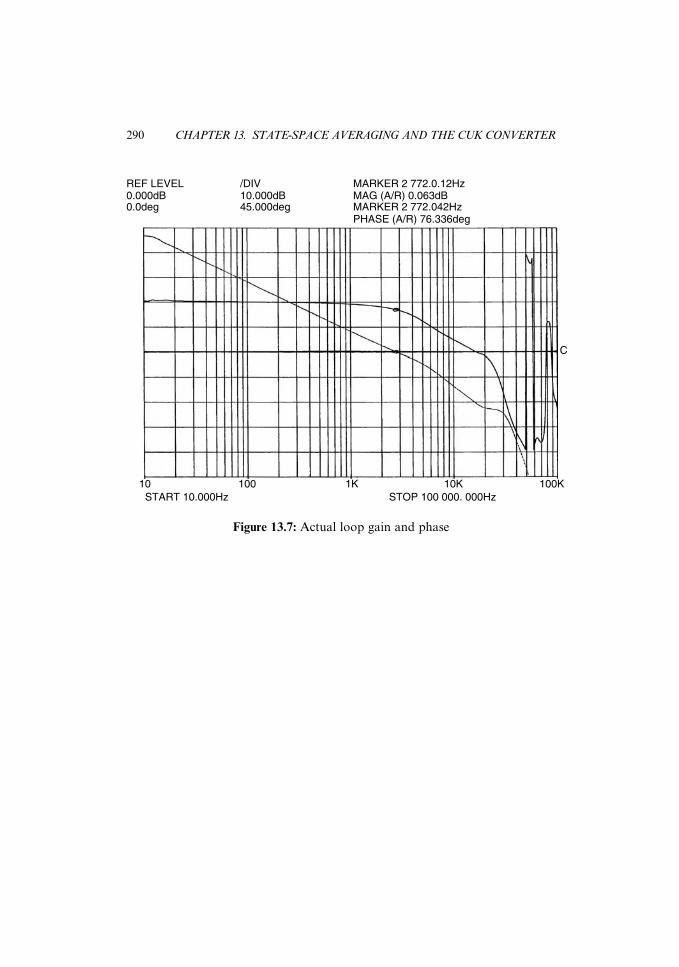
10 100 1K 10K 100KSTART 10.000Hz STOP 100 000. 000Hz
REF LEVEL0.000dB0.0deg
/DIV10.000dB45.000deg
MARKER 2 772.0.12HzMAG (A/R) 0.063dBMARKER 2 772.042HzPHASE (A/R) 76.336deg
C
Figure 13.7: Actual loop gain and phase
290 CHAPTER 13. STATE-SPACE AVERAGING AND THE CUK CONVERTER

Chapter 14
Simulation
With the advance of digital computers, simulation has made giant strides
in the past 20 or 30 years in all scientific and technical fields. In the late
1970s, for electrical circuit analysis using computer, one dialed the
Control Data Corporation (CDC) with a modem-equipped portable
terminal/keyboard, edited the circuit file one component (one line) at a
time, debugged the file for syntax errors, ran the file for half an hour or
so and ran up a phone bill by the minute, read the dot-matrix printout,
and repeated the simulation until the desired, appropriately formatted
hard copy was obtained. In the end, the whole effort might take hours, if
not all night. By 1990, the same study was regularly done on a personal
computer and took only a few minutes to produce a colorful printout.
This advancement prompted many new generations of electrical engin-
eers to flock to PC-based circuit simulators and to believe that all circuits
can be studied using simulation software like Spice or its derivatives.
Following the same line of logic, many designers working on switch-
mode power converters also quickly converged or on the idea: electronic
breadboarding and testing.
However, as rapidly the simulation wildfire spread, numerous diffi-
culties arose. Among the most troublesome was the convergence issue
the simulator faced when solving tens of differential equations that
described a complex circuit based on Kirchoff’s current and voltage
laws. Basically, those differential equations in discrete form were solved
at finite time points starting from time zero and zero initial conditions,
291

zero voltage across capacitors, and zero current through inductors. At
every time step, every circuit loop must give a zero voltage sum while
every node must give a zero current sum. If one step out of tens of
equations fails to meet the constraint, it is considered a violation and
the simulation just stops and reports ‘‘fails to converge at time . . . ’’
Switch-mode converters are particularly prone to such a simulation
failure for multiple reasons.
By now, we understand that switch-mode converters are highly non-
linear because of magnetic devices with nonlinear magnetic cores, diodes,
and transistors operating in on/off mode. It is also not uncommon for
modern converters to operate at hundreds of kilohertz. At that fre-
quency, a switching cycle lasts only a fraction of a microsecond. Then,
to observe circuit behavior accurately, the sampling rate is selected to be
high. That is to say, a computation time resolution on the order of only
several nanoseconds is the rule rather than exception. Even more
demanding is that fixed-step technology often does not handle switch
transition edges well. Because of this latter concern, a variable time step
is often invoked autonomously at transitions. In theory, the variable step
should work better. But in reality, the variable step is still constrained by
an absolute minimum step that is the nature of digital computers. Yes,
variable-step methods may better capture transitional behavior, but it
also unwillingly introduces a higher probability of discontinuity in state
transitions and precipitates divergence.
In this chapter, we introduce a compromise, an approach that avoids
divergence but suffers minor inaccuracy. We dive into the problem
without further verbiage.
14.1 Dynamic Equations for a Forward Converterwith Voltage-Mode Control
Figure 14.1 gives an isolated forward converter with voltage-mode con-
trol using an external oscillator.
A total of 10 state variables need to be accounted for: the input
inductor current, i1; the primary voltage, vp; the output inductor current,
292 CHAPTER 14. SIMULATION

i; the output voltage, vo; the output filter damping voltage, vcd ; three
voltages associated with the error amplifier, va, vb, and ve; the trans-
former magnetizing current, im; and the input filter damping voltage,
vid . The input loop gives
L1
di1
dtþ r1 . i1 þ vp ¼ Vin (14:1)
This can be easily placed in a discrete form for a small time step dt and
step index j:
(i1)jþ1 ¼ 1� r1 . dt
L1
� �(i1)j �
dt
L1
(vp)j þdt
L1
Vin (14:2)
We can do the same for the primary node:
C1
dvp
dtþ vp � vid
Rd2
þ ip ¼ i1 (14:3)
vs Vo
N1 N2
Vin + −
is
i
ip
+
-
R30
R28C15
Ts
ve
vr
Driver va
vfkf
R29C3
C1
LL1
vb
Rd
Cd
C
r1 rvp
vcd
RL
ve
On Off
C16
i1
Rd2
C2
vid
Error−
amp.+
Figure 14.1: Isolated forward converter with voltage-mode control
14.1. DYNAMIC EQUATIONS FOR A FORWARD CONVERTER 293

the output loop:
Ldi
dtþ r . i þ vo ¼ vs (14:4)
the output node:
Cdvo
dtþ vo � vcd
Rd
þ vo
RL
¼ i (14:5)
the output damping node:
Cd
dvcd
dt¼ vo � vcd
Rd
(14:6)
the feedback path (vr constant):
vf ¼ kf. vo
C3
d(va � vr)
dt¼ C3
dva
dt¼ vf � va
R29
C15
d(vb � ve)
dt¼ C15
dvb
dt� C15
dve
dt¼ vr � vb
R28
C16
d(vr � ve)
dtþ vr � vb
R28
¼ �C16
dve
dtþ vr � vb
R28
¼ vf � vr
R30
þ vf � va
R29
(14:7)
the primary magnetization loop:
Lm
dim
dtþ Rswitch im þ
N2
N1
is
� �¼ vp (14:8)
294 CHAPTER 14. SIMULATION
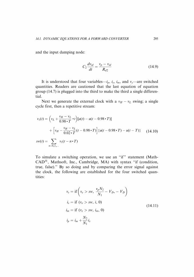
and the input damping node:
C2
dvid
dt¼ vp � vid
Rd2
(14:9)
It is understood that four variables—ip, is, im, and vs—are switched
quantities. Readers are cautioned that the last equation of equation
group (14.7) is plugged into the third to make the third a single differen-
tial.
Next we generate the external clock with a vH � vL swing; a single
cycle first, then a repetitive stream:
v1(t) ¼ vL þvH � vL
0:98 . T. t
� �[u(t)� u(t� 0:98 . T)]
þ vH �vH � vL
0:02 . T(t� 0:98 . T)
h i{u(t� 0:98 . T)� u(t� T)}
sw(t) ¼X
n¼0,1,...v1(t� n . T)
(14:10)
To simulate a switching operation, we use an ‘‘if ’’ statement (Math-
CAD1, Mathsoft, Inc., Cambridge, MA) with syntax ‘‘if (condition,
true, false).’’ By so doing and by comparing the error signal against
the clock, the following are established for the four switched quan-
tities:
vs ¼ if ve > sw,vpN2
N1
� VD,� VD
� �
is ¼ if (ve > sw, i, 0)
im ¼ if (ve > sw, im, 0)
ip ¼ im þN2
N1
is
(14:11)
14.1. DYNAMIC EQUATIONS FOR A FORWARD CONVERTER 295

Some practical facts must also be considered. These include the
power supply limiting for the error amplifier and consequently the
error voltage <15V and built-in duty-cycle limiting <3:3 V for 50%.
Once these limiting factors are incorporated, (14.11) becomes
vs ¼ if if(ve > 3:3, 3:3, ve) > sw,vpN2
N1
� VD,�VD
� �
is ¼ if [if(ve > 3:3, 3:3, ve) > sw, i, 0] (14:12)
im ¼ if [if(ve > 3:3, 3:3, ve) > sw, im, 0]
ip ¼N2
N1
is þ im
Furthermore, considering the existence of losses in the primary side, the
effective voltage available for energy transfer is reduced. In other words,
the effective primary voltage accounts for losses and is represented in the
following form
vp � Rswitch
N2
N1
if [if(ve > 3:3, 3:3, ve) > sw, i, 0]þ im
� �(14:13)
With all the pertinent equations and switching functions formulated,
(14.3) through (14.13) should also be placed in discrete form, just as
(14.2) did for (14.1). All discrete equations are then arranged in a
seeded iteration form. (Since the iteration formulation involves both
the primary and the secondary subscripts that do not use typing space
effectively, the following ignores the primary subscript and keeps
only the time step index, j, as a subscript.) The form is ready for
simulation with the following components and operating parameters:
Ron ¼ Rswitch ¼ 0:01, Lm ¼ 1 mH, Vin ¼ 28V, L1 ¼ 3:5 mH, r1 ¼ 0:01,
C1 ¼ 68 mF, C2 ¼ 3� C1, Rd2 ¼ 4:7, Vd(rectifier) ¼ 0:7, N1 ¼ 13,
N2¼ 18, Vr ¼ 2:5, i28 ¼ 63:4 K, R29 ¼ 1:13K, R30 ¼ 12:7 K, i3 ¼ 4700
�3 pF, L ¼ 5:76mH, r ¼ 0:005, RL ¼ 33, C ¼ 22 mF, Cd ¼ 120 mF,
Rd ¼ 12:7, T ¼ 10:4 ms, dt ¼ 0:02T, kf ¼ 0:2515, vH ¼ 5:692, and
vL ¼ 1.
296 CHAPTER 14. SIMULATION

iljþ
1
vpjþ
1
i jþ
1
vojþ
1
vcd
jþ1
vajþ
1
vbjþ
1
vejþ
1
imjþ
1
vid
jþ1
0 B B B B B B B B B B B B B B B B B B B B B B B B @
1 C C C C C C C C C C C C C C C C C C C C C C C C A¼
i1jþ
[Vin�
(r1
.il
jþ
vpj)].
dt
L1
vpjþ
ilj�
vpj�
vid
j
Rd2þ
N2
N1
.if
(if(
vej
$3:3
,3:3
,ve j
)>
swj,i j,0
)þ
imj
��
��
�� .
dt
C1
i jþ
dt
L1
.if
if( v
e j$
3:3
,3:3
,ve j
)>
swj,
N2
N1
��
.vp
j�
Ron
N2
N1
.if
(if(
vej
$3:3
,3:3
,ve j
)>
swj,i j,0
)þ
imj
��
�� �V
d,�
Vd
� �(r
.i jþ
voj)
�
vojþ
dt
C.
i j�
voj�
vcd
j
Rd
þvo
j
RL
��
��
vcd
jþ
dt
Cd
.vo
j�
vcd
j
Rd
vajþ
dt
C3
.kf
.vo
j�
vaj
R29
vbjþ
dt
.V
r�
vbj
R28C
16�
kf
.vo
j�
Vr
R30C
16�
kf
.vo
j�
vaj
R29C
16þ
Vr�
vbj
R28C
15
��
ifve
j>
15,1
5,v
e jþ
dt
C16
.V
r�
vbj
R28�
kf
.vo
j�
Vr
R30
�kf
.vo
j�
vaj
R29
��
��
ifif
( ve j
$3:3
,3:3
, ve j
)>
swj,im
jþ
dt
Lm
.vp
j�
N2
N1
.if
(if(
vej
$3:3
,3:3
, ve j
)>
swj,i j,0
)þ
imj
�� .
Ron
�� ,0
��
vid
jþ
dt
C2
.vp
j�
vid
j
Rd2
2 6 6 6 6 6 6 6 6 6 6 6 6 6 6 6 6 6 6 6 6 6 6 6 6 6 6 6 6 6 6 6 6 6 6 6 6 6 6 6 6 6 6 6 6 6 6 6 6 6 4
3 7 7 7 7 7 7 7 7 7 7 7 7 7 7 7 7 7 7 7 7 7 7 7 7 7 7 7 7 7 7 7 7 7 7 7 7 7 7 7 7 7 7 7 7 7 7 7 7 7 5

14.2 Turn-on Forward Converter with Voltage-ModeControl
The forward converter is turned on with an all-zero initial state. The
simulation runs for 200 clock cycles and produces an end state. Figure
14.2 shows major node voltages and branch currents identified in
Figure 14.1.
14.3 Steady-State Forward Converter with Voltage-Mode Control
The end state produced by the initial turn-on run is passed along to the
next 200 cycles as the starting state. The end state of the second 200-cycle
run is then used as the starting state for the third 200-cycle run. This
repeats until the end state no longer changes. A consistent end state
signifies the steady state.
14.4 Steady State, Zoomed In
To observe the waveform details, a 10 cycle run under the steady state is
performed. Figure 14.4 shows the end result.
Figure 14.4 shows signs of subharmonic oscillation at about 10 KHz.
This is attributed to the low-phase margin at that closed-loop frequency.
Certainly, the error amplifier should be improved. However, that is not
the goal of this chapter. This chapter shows another way to perform
simulation. Before closing the present section, it is very instructive to
observe the actions of voltage-mode pulse-width modulation. This is
done by superimposing the clock and the error voltage on the same
plot (Figure 14.5).
298 CHAPTER 14. SIMULATION

−2
0
2
4
6
Inpu
t cur
rent
6
−2
i1j
0 tj
0
1
2
3
4
Prim
ary
/ sw
itch
curr
ent
4
0
ipj
0 tj
0
15
30
45
60
Sec
onda
ry v
olta
ge
60
0
vsj
(m + 1) .T
(m + 1) .T
(m + 1) .T
0 tj
Figure 14.2: Initial turn-on forward converter with voltage-mode control
14.4. STEADY STATE, ZOOMED IN 299

0
0.5
1
1.5
2
Sec
onda
ry c
urre
nt
2
0
isj
(m + 1) .T
(m + 1) .T
(m + 1) .T
(m + 1) .T
0 tj
0
0.5
1
1.5
2
Fre
e-w
heel
dio
de c
urre
nt
2
0
idj
0 tj
0
0.5
1
1.5
2
Out
put i
nduc
tor
curr
ent
2
0
ij
0 tj
0
4
8
12
16
Out
put v
olta
ge
16
0
voj
0 tj
Figure 14.2: Continued
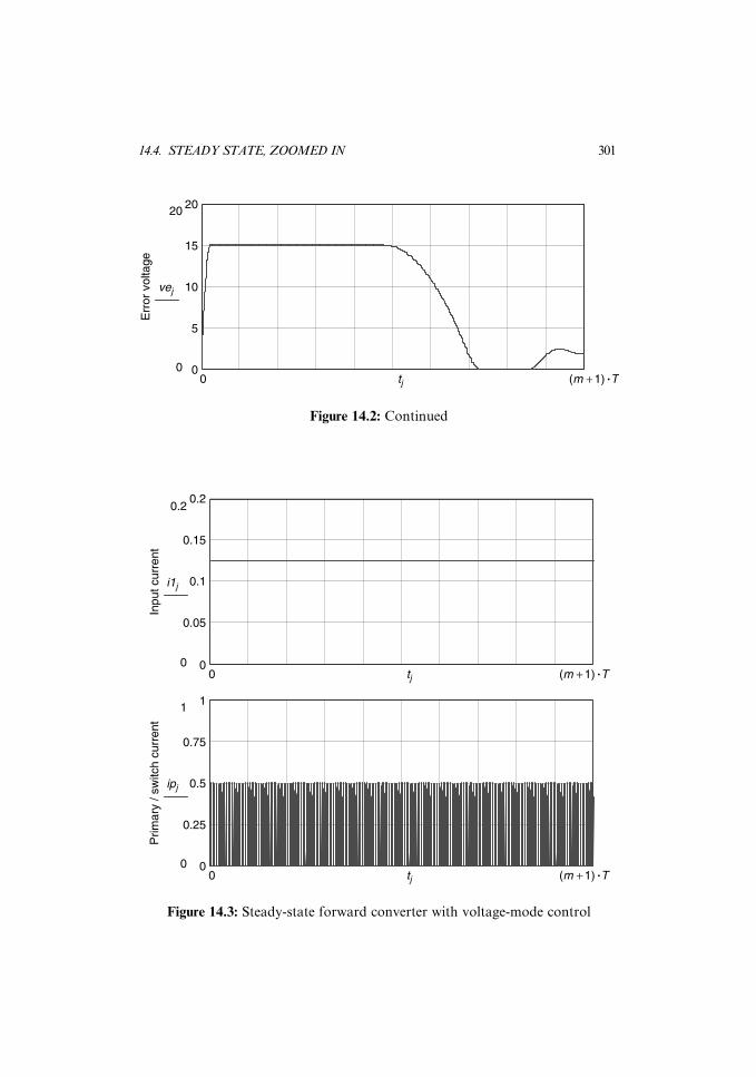
0
5
10
15
20
Err
or v
olta
ge
20
0
vej
(m + 1) .T0 tj
Figure 14.2: Continued
0
0.05
0.1
0.15
0.2
Inpu
t cur
rent
0.2
0
i1j
(m + 1) .T0 tj
0
0.25
0.5
0.75
1
Prim
ary
/ sw
itch
curr
ent
1
0
ipj
(m + 1) .T0 tj
Figure 14.3: Steady-state forward converter with voltage-mode control
14.4. STEADY STATE, ZOOMED IN 301
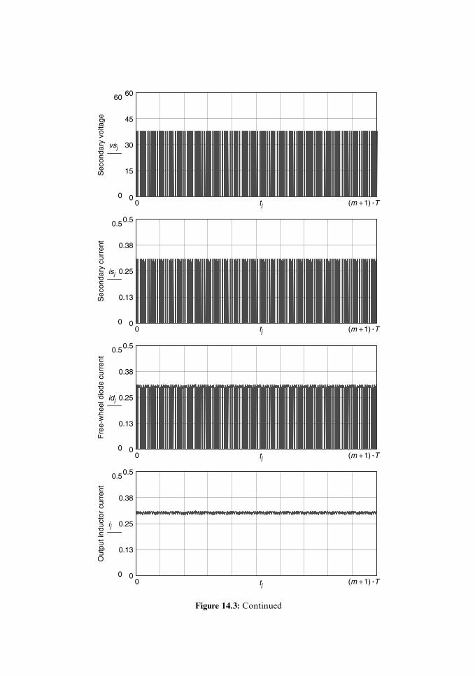
0
15
30
45
60S
econ
dary
vol
tage
60
0
vsj
(m + 1) .T0 tj
tj
tj
tj
0
0.13
0.25
0.38
0.5
Sec
onda
ry c
urre
nt
0.5
0
isj
(m + 1) .T0
0
0.13
0.25
0.38
0.5
Fre
e-w
heel
dio
de c
urre
nt
0.5
0
idj
(m + 1) .T0
0
0.13
0.25
0.38
0.5
Out
put i
nduc
tor
curr
ent
0.5
0
ij
(m + 1) .T0
Figure 14.3: Continued

14.5 Load-Transient Forward Converter withVoltage-Mode Control
Figure 14.6 shows the converter performance when subjected to a step
load increase, RL, from 33 to 23.
Figure 14.7 shows the converter performance when subjected to a
step load decrease, RL, from 33 to 40.
A similar transient response can be performed by changing Vin from
28 volts to 30 volts or from 28 volts to 26 volts in step.
0
4
8
12
16
Out
put v
olta
ge
16
0
voj
(m + 1) .T0 tj
0
1
2
3
4
Err
or v
olta
ge
4
0
vej
(m + 1) .T0 tj
Figure 14.3: Continued
14.5. LOAD-TRANSIENT FORWARD CONVERTER 303
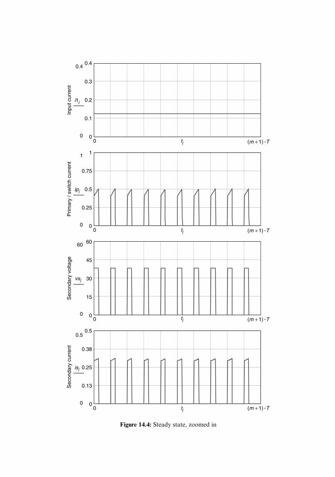
0
0.1
0.2
0.3
0.4In
put c
urre
nt0.4
0
i1j
0 tj
0
0.25
0.5
0.75
1
Prim
ary
/ sw
itch
curr
ent
1
0
ipj
0 tj
0
15
30
45
60
Sec
onda
ry v
olta
ge
60
0
vsj
0 tj
0
0.13
0.25
0.38
0.5
Sec
onda
ry c
urre
nt
0.5
0
isj
(m + 1) .T
(m + 1) .T
(m + 1) .T
(m + 1) .T
0 tj
Figure 14.4: Steady state, zoomed in

0
0.13
0.25
0.38
0.5F
ree-
whe
el d
iode
cur
rent
0.5
0
idj
(m + 1) .T0 tj
0
0.13
0.25
0.38
0.5
Out
put i
nduc
tor
curr
ent
0.5
0
ij
(m + 1) .T0 tj
9.92
9.93
9.94
9.95
9.96
Out
put v
olta
ge
9.96
9.92
voj
(m + 1) .T0 tj
2.2
2.23
2.25
2.27
2.3
Err
or v
olta
ge
2.3
2.2
vej
(m + 1) .T0 tj
Figure 14.4: Continued

14.6 Dynamic Equations for a Forward Converterwith Peak Current-Mode Control
The section presents the current-mode control. Figure 1.30 is expanded
and component symbols are reassigned for consistency with the author’s
existing simulation file. This results in Figure 14.8. Since we already went
through the step showing how the dynamic equations governing a con-
verter are written, we will not repeat the step for this section.
However, an important feature of this circuit requires attention. As
shown, the current feedback is compared with the effective error voltage,
veff . When the current feedback intercepts the effective error, the com-
parator output swings to high from low. In practice, this low to high
transition must be used somehow to terminate the power switch’s con-
duction. Paradoxically, the conduction termination of the power switch
quickly pulls the current feedback below the effective error. Thus, the
comparator output also quickly changes state and swings to low. In other
words, the comparator output exhibits a positive-going pulse of ex-
tremely short duration. This short pulse signals only the time of thresh-
old crossing and is not suitable for commanding the power switch. As an
effective pulse-width modulator, the short pulse must be converted into
an appropriate on/off control with the right duration. This is done by a
reset set flip-flop (RSFF) (Figure 14.9).
0
1.5
3
4.5
6
Err
or v
olta
ge
6
0
vej
swj
(m + 1) .T0 tj
Figure 14.5: Voltage-mode pulse-width modulation
306 CHAPTER 14. SIMULATION

0
0.075
0.15
0.22
0.3
Inpu
t cur
rent
0.3
0
i1j
0 tj
0
0.25
0.5
0.75
1
Prim
ary
/ sw
itch
curr
ent
1
0
ipj
0 tj
0
0.13
0.25
0.38
0.5
Sec
onda
ry c
urre
nt
0.5
0
isj
0 tj
0
0.13
0.25
0.38
0.5
Out
put i
nduc
tor
curr
ent
0.5
0
ij
(m + 1) .T
(m + 1) .T
(m + 1) .T
(m + 1) .T
0 tj
Figure 14.6: Transient load increase

The RSFF accepts two inputs: R, the error-crossing intercept, and S,
an external-pulse clock train. Mathematically, the RSFF’s Q output can
be expressed as
Qjþ1 ¼ Rj [ (Qj [ Sj) (14:14)
We give here the discrete seeded iteration equations in their entirety
without further procedural writing. The first equation is the expanded
form of (14.14). It shall also be noted that, in the first equation, the
effective error voltage is limited to larger than zero but less than 1 volt.
0
4
8
12
16
Out
put v
olta
ge
16
0
voj
(m + 1) .T0 tj
0
1
2
3
4
Err
or v
olta
ge
4
0
vej
(m + 1) .T0 tj
Figure 14.6: Continued
308 CHAPTER 14. SIMULATION

0
0.075
0.15
0.22
0.3In
put c
urre
nt0.3
0
i1j
(m + 1) .T0 tj
0
0.25
0.5
0.75
1
Prim
ary
/ sw
itch
curr
ent
1
0
ipj
(m + 1) .T0 tj
0
0.13
0.25
0.38
0.5
Sec
onda
ry c
urre
nt
0.5
0
isj
(m + 1) .T0 tj
0
0.13
0.25
0.38
0.5
Out
put i
nduc
tor
curr
ent
0.5
0
ij
(m + 1) .T0 tj
Figure 14.7: Transient load decrease

14.7 Simulation, Forward Converter with PeakCurrent-Mode Control
All simulations are performed with the following component values
and operating parameters: N1 ¼ 19, N2 ¼ 12, Lm ¼ 1150 nH, rw ¼ 0:1,
Ron ¼ 0:2, L1 ¼ 102 mH, rL1 ¼ 0:005, Vin ¼ 28, L2 ¼ 385 mH, rL2
¼ 0:077, RL ¼ 5:3=2:5, C9 ¼ 200 mF, rC1 ¼ 0:05, VD ¼ 0:5, Vref ¼ 2:5,
R35 ¼ 9:76K, R70 ¼ 11:1 K, Rsen ¼ 36:5, ni ¼ 100, R12 ¼ 2 K, R45
¼ 24:3 K, C37 ¼ 560 pF, C29 ¼ 2200 pF, R43 ¼ 10K, Vbe ¼ 0:7,
R20 ¼ 5:11K, R33 ¼ 2:94K, hfe ¼ 150, R19 ¼ 5:11K, R31 ¼ 6:65K,
R39 ¼ 33:2K, C39 ¼ 560 pF, C7 ¼ 60 mF, rC2 ¼ 2:61, and C8 ¼ 60 mF.
The initial turn-on is conducted with a zero starting state for 200
switching cycles (Figure 14.10) at 125 KHz. After 400 cycles, it reaches
0
4
8
12
16
Out
put v
olta
ge
16
0
voj
(m + 1) .T0 tj
0
1
2
3
4
Err
or v
olta
ge
4
0
vej
(m + 1) .T0 tj
Figure 14.7: Continued
310 CHAPTER 14. SIMULATION

+−+ −
+ −
R70 R35
R43
R20
R33 R
79
R31
R39
R
2Rv e
v er
Vre
f
2.5V
v o
PW
M
SG
1843
19T
12T
v o
RL
Rse
n
Cur
rent
feed
back
Isol
ated
gate
driv
er
Vin
n i
Q
N1
N2
i p
A
C39
L 2, r
L2L 1
, rL1
i 2 r C2
C7
C8
L mi m
v 4
v 3C
9
C29
C37
R45
v 2
v 1r C
1
i 1
v eff
10V
RS
FF
1V Fig
ure
14.8
:Is
ola
ted
forw
ard
conver
ter
with
pea
kcu
rren
t-m
ode
contr
ol

qjþ
1
i1jþ
1
v1jþ
1
v2jþ
1
vejþ
1
ver jþ
1
i2jþ
1
v3jþ
1
v4jþ
1
imjþ
1
2 6 6 6 6 6 6 6 6 6 6 6 6 6 6 6 6 6 6 6 6 6 6 6 6 6 6 6 4
3 7 7 7 7 7 7 7 7 7 7 7 7 7 7 7 7 7 7 7 7 7 7 7 7 7 7 7 5:¼
�if
Rse
n
ni
.im
jþ
N2
N1
.i1
j.q
j
�� $
if(v
erj�
2.V
D)
.1 3
$1,1
,if
(ver
j�
2.V
D)
.1 3
��
���
<0,0
,(ve
r j�
2.V
D)
.1 3
�� ,1,0
�� _�
[qj_
(if(c
lkj¼
1,1
,0))
]�
i1jþ
dt
.�
rL1þ
Rp
L1
�� .
i1j�
k L1
.v1
jþ
1 L1
.if
qj¼
0,�
VD
,N2
v4j�
(rwþ
Ron)
.im
jþ
N2
N1
.i1
j.q
j
��
N1
�V
D
��
��
v1jþ
dt
.R
p
rc1
.C
9.i1
jþ
k�
1
rc1
.C
9.v1
j
��
v2jþ
dt
.�
kf
.R
p
(R12C
37)
.i1
jþ�
kf
.k
R12C
37
.v1
j�
1
(R45C
37)þ
1
R45C
29
�� .
v2jþ
1
(R12C
37)þ
1
(R45C
37)þ
1
R45C
29
�� .
Vre
f
��
ifve
j>
5,5
,if
vej<
0,0
,ve jþ
dt
.�
kf
.R
p
(R12C
37)
.i1
jþ�
kf
.k
R12C
37
.v1
j�
1
(R45C
37)
.v2
jþ
1
(R12C
37)þ
1
(R45C
37)
�� .
Vre
f
��
��
��
ifve
r i>
10,1
0,if
ver j<
0,0
,ver
jþ
dt
.�
GT
R31C
39
.ve
j�
1
R39C
39
.ve
r jþ
1
(R31)þ
1
(R39)
�� .
1
C39
.V
ref�
1
R31C
39
.V
bia
s
��
��
��
i2jþ
dt
.�
rL2
L2
.i2
j�
1 L2
.v4
jþ
1 L2
.V
in
��
v3jþ
dt
.�
1
rc2
.C
7.v3
jþ
1
rc2
.C
7.v4
j
��
v4jþ
dt
.1 C8
.i2
jþ
1
rc2
.C
8.v3
j�
1
rc2
.C
8.v4
j�
1 C8
.im
jþ
N2
N1
.i1
j.q
j
��
��
ifq
j¼
0,0
,im
jþ
dt
Lm
.v4
j�
(rwþ
Ron)
.im
jþ
N2
N1
.i1
j.q
j
��
��
��
2 6 6 6 6 6 6 6 6 6 6 6 6 6 6 6 6 6 6 6 6 6 6 6 6 6 6 6 6 6 6 6 6 6 6 6 6 6 6 6 6 6 6 6 6 6 6 6 6 6 6 6 6 6 6 6 4
3 7 7 7 7 7 7 7 7 7 7 7 7 7 7 7 7 7 7 7 7 7 7 7 7 7 7 7 7 7 7 7 7 7 7 7 7 7 7 7 7 7 7 7 7 7 7 7 7 7 7 7 7 7 7 7 5

the steady state (Figure 14.11). Figure 14.12 gives steady state zoomed in
for 10 cycles. When subjected to a step load increase from 2.5 A to 2.6 A,
the converter behaves very well (Figure 14.13). The same can also be said
for a step load decrease from 2.5 A to 2.3 A (Figure 14.14). Both load
transient responses settle in about 30 cycles.
14.8 State Transition Technique: Accelerated SteadyState
In Sections 1.14, 3.7, and 5.7, we used state transition techniques and the
concept of the continuity of state repeatedly to obtain the steady-state
outputs (responses) of several simple circuits driven by periodic sources.
Given its powerful utility, there is no reason the approach should be
limited to dealing merely with simple circuits.
We also noted that simulation, either with commercially available
software tools or custom-made programs given in the past several sec-
tions, must pass the transient phase. Not only does the transient phase
invite trouble, as stated in the introduction of this chapter, it also wastes
precious simulation time.
We now show that the state transition methods and the concept of the
continuity of state can be just as effective in dealing with a complete
converter, while bypassing the transient phase in the process.
Referring to Figure 14.15, which is based on Figure 14.8 with the
input filter added, we assign nine state variables: i1, the output filter
choke current; v1, the output filter capacitor voltage; v2, the error amp-
lifier feedback capacitor voltage; vn, the inverting node voltage of the
error amplifier; vn2, the inverting node voltage of the PWM built-in error
amplifier; i2, the input filter choke current; v3, the input filter capacitor
voltage; v4, the primary winding voltage; and im, the primary magnetizing
R
S Q
Q
Figure 14.9: RSFF
14.8. STATE TRANSITION TECHNIQUE: ACCELERATED STEADY STATE 313

0
0.5
1
1.5
2P
WM
, RS
FF
Q o
utpu
t2
0
qj
(m + 1) .T0 tj
0
4
8
12
16
Inpu
t cur
rent
16
0
i2j
0
(m + 1) .T0 tj
0
1
2
3
4
Prim
ary/
switc
h cu
rren
t
4
0
ipj
(m + 1) .T0 tj
0
10
20
30
40
Sec
onda
ry v
olta
ge
40
0
v secj
(m + 1) .T0 tj
Figure 14.10: Initial turn-on forward converter with peak current-mode
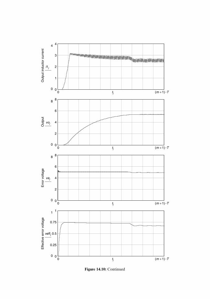
0
1
2
3
4O
utpu
t ind
ucto
r cu
rren
t4
0
i1j
(m + 1) .T0 tj
0
2
4
6
8
Out
put
8
0
voj
(m + 1) .T0 tj
0
2
4
6
8
Err
or v
olta
ge
8
0
vej
(m + 1) .T0 tj
0
0.25
0.5
0.75
1
Effe
ctiv
e er
ror
volta
ge
1
0
veffj
(m + 1) .T0 tj
Figure 14.10: Continued
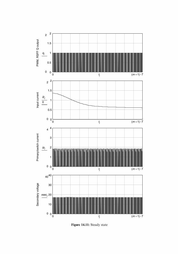
0
0.5
1
1.5
2P
WM
, RS
FF
Q o
utpu
t2
0
qj
(m + 1) .T0 tj
0
0.5
1
1.5
2
Inpu
t cur
rent
2
0
i2j
0
(m + 1) .T0 tj
0
1
2
3
4
Prim
ary/
switc
h cu
rren
t
4
0
ipj
(m + 1) .T0 tj
0
10
20
30
40
Sec
onda
ry v
olta
ge
40
0
vsecj
(m + 1) .T0 tj
Figure 14.11: Steady state
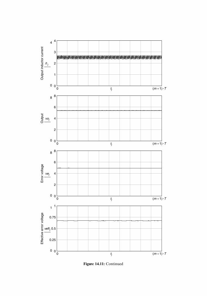
0
1
2
3
4O
utpu
t ind
ucto
r cu
rren
t4
0
i1j
(m + 1) .T0 tj
0
2
4
6
8
Out
put
8
0
voj
(m + 1) .T0 tj
0
2
4
6
8
Err
or v
olta
ge
8
0
vej
(m + 1) .T0 tj
0
0.25
0.5
0.75
1
Effe
ctiv
e er
ror
volta
ge
1
0
veffj
(m + 1) .T0 tj
Figure 14.11: Continued

0
0.5
1
1.5
2P
WM
, RS
FF
Q o
utpu
t
2
0
qj
(m + 1) .T0 tj
0
0.25
0.5
0.75
1
Inpu
t cur
rent
1
0
i2j
0
(m + 1) .T0 tj
0
1
2
3
4
Prim
ary
/ sw
itch
curr
ent
4
0
ipj
(m + 1) .T0 tj
0
10
20
30
40
Sec
onda
ry v
olta
ge
40
0
vsecj
(m + 1) .T0 tj
Figure 14.12: Steady state, zoomed in

0
1
2
3
4O
utpu
t ind
ucto
r cu
rren
t4
0
i1j
(m + 1) .T0 tj
0
1.5
3
4.5
6
Out
put
6
0
voj
(m + 1) .T0 tj
4.8
4.85
4.9
4.95
5
Err
or v
olta
ge
5
4.8
vej
(m + 1) .T0 tj
0
0.25
0.5
0.75
1
Effe
ctiv
e er
ror
volta
ge
1
0
veffj
(m + 1) .T0 tj
Figure 14.12: Continued
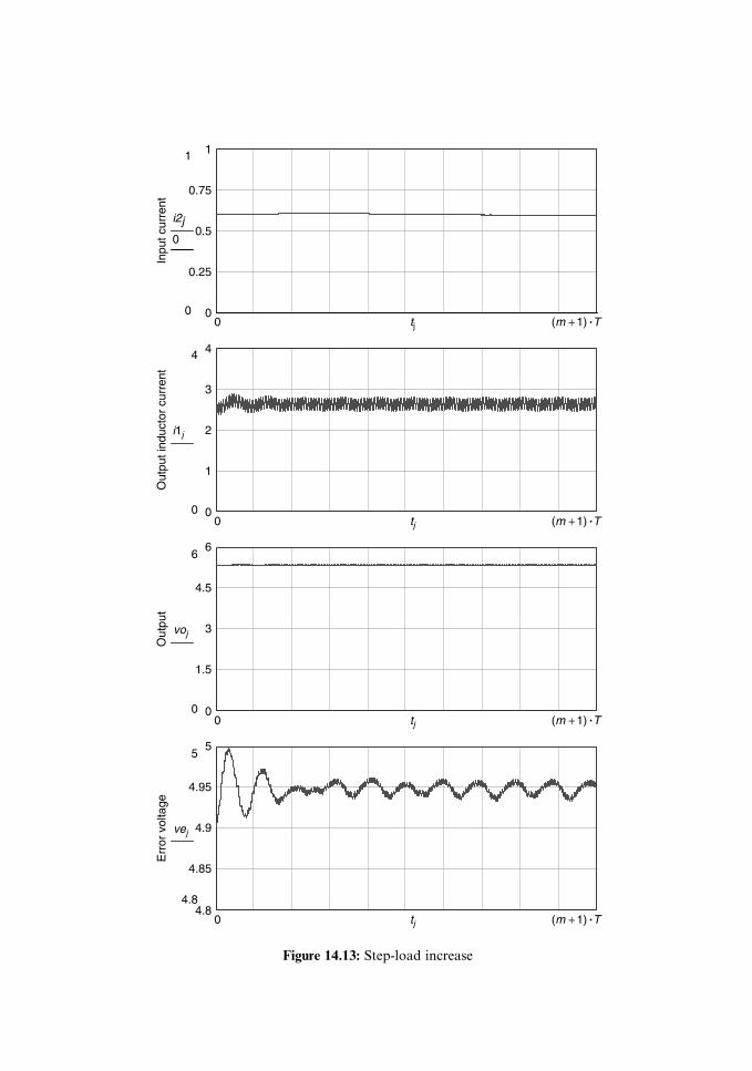
0
0.25
0.5
0.75
1In
put c
urre
nt1
0
i2j
0
(m + 1) .T0 tj
0
1
2
3
4
Out
put i
nduc
tor
curr
ent
4
0
i1j
(m + 1) .T0 tj
0
1.5
3
4.5
6
Out
put
6
0
voj
(m + 1) .T0 tj
4.8
4.85
4.9
4.95
5
Err
or v
olta
ge
5
4.8
vej
(m + 1) .T0 tj
Figure 14.13: Step-load increase

current. Without going through the derivations of the state equation one
by one for all nine variables, we simply give the state matrix correspond-
ing to switch, Q, on and off.
During switch-on, the state transition equation in differential form is
dx=dt ¼ A1xþ B; the source matrix and source are consolidated in a
single matrix B. The state column matrix (vector) is
x ¼ i1 v1 v2 vn vn2 i2 v3 v4 im½ �T
A1 ¼
a111 a112 0 0 0 0 0 a118 a119
a121 a122 0 0 0 0 0 0 0
a131 a132 a133 a134 0 0 0 0 0
a141 a142 a143 a144 0 0 0 0 0
0 0 0 a154 a155 0 0 0 0
0 0 0 0 0 a166 0 a168 0
0 0 0 0 0 0 a177 a178 0
a181 0 0 0 0 a186 a187 a188 a189
a191 0 0 0 0 0 0 a198 a199
266666666666666664
377777777777777775
0
0.25
0.5
0.75
1
Effe
ctiv
e er
ror
volta
ge
1
0
veffj
(m + 1) .T0 tj
Figure 14.13: Continued
14.8. STATE TRANSITION TECHNIQUE: ACCELERATED STEADY STATE 321

0
0.25
0.5
0.75
1In
put c
urre
nt1
0
i2j
0
(m + 1) .T0 tj
0
1
2
3
4
Out
put i
nduc
tor
curr
ent
4
0
i1j
(m + 1) .T0 tj
0
1.5
3
4.5
6
Out
put
6
0
voj
(m + 1) .T0 tj
4.6
4.7
4.8
4.9
5
Err
or v
olta
ge
5
4.6
vej
(m + 1) .T0 tj
Figure 14.14: Step-load decrease

where
a111 ¼�rL1 þ Rp þ N2
N1
� �2
(rw þ Ron)
L1
, a112 ¼ �k
L1
, a118 ¼N2
L1N1
,
a119 ¼�N2(rw þ Ron)
L1N1
, a121 ¼Rp
rC1C9
, a122 ¼k� 1
rC1C9
,
a131 ¼�A . kf
.Rp
(1þ A)R12C37
, a132 ¼�A . kf
.k
(1þ A)R12C37
,
a133 ¼�A
(1þ A)R45C37
� 1
R45C29
,
a134 ¼A
(1þ A)C37
1
R12
þ 1
R45
þ 1þ A
Rx
� �þ 1
R45C29
,
a141 ¼kf
. Rp
(1þ A)R12C37
, a142 ¼kf
. k
(1þ A)R12C37
,
a143 ¼1
(1þ A)R45C37
, a144 ¼ �1
(1þ A)C37
1
R12
þ 1
R45
þ 1þ A
Rx
� �
0
0.25
0.5
0.75
1
Effe
ctiv
e er
ror
volta
ge
1
0
veffj
(m + 1) .T0 tj
Figure 14.14: Continued
14.8. STATE TRANSITION TECHNIQUE: ACCELERATED STEADY STATE 323

a154 ¼hfe
R31R19
R31 þ R19
(1þ A)R31C39
Kb2, a155 ¼
R19
(R19 þ R31)R31
� 1
R31
� 1þ A
R39
(1þ A)C39
,
a166 ¼�rL2
L2
, a168 ¼ �1
L2
, a177 ¼ �1
rC2C7
, a178 ¼1
rC2C7
,
a181 ¼�N2
N1C8
, a186 ¼1
C8
, a187 ¼1
rC2C8
, a188 ¼ �1
rC2C8
,
a189 ¼�1
C8
, a191 ¼�N2(rw þ Ron)
N1Lm
, a198 ¼1
Lm
,
a199 ¼�(rw þ Ron)
Lm
,
B ¼
�VD
L1
0
�A2Vref
(1þ A)RxC37
A . Vref
(1þ A)RxC37
hfe
R31R19
R31 þ R19
(1þ A)R31C39
Kb1 þA .Vref
(1þ A)R39C39
Vin
L2
0
0
0
26666666666666666666666666666664
37777777777777777777777777777775
,
kf ¼R35
R35 þ R70, Rp ¼
rC1RL
rC1 þ RL
, k ¼ RL
rC1 þ RL
,
Kb2 ¼A .R20
R20R43 þ (1þ hfe)R33(R20 þ R43),
Kb1 ¼�R43(10� VD)þ (R20 þ R43)(10� Vbe)� A . R20 . Vref
R20R43 þ (1þ hfe)R33(R20 þ R43)
During switch-off, the state transition equation in differential form is
dx=dt ¼ A2xþ B:
324 CHAPTER 14. SIMULATION

A2 ¼
a211 a212 0 0 0 0 0 0 0
a221 a222 0 0 0 0 0 0 0
a231 a232 a233 a234 0 0 0 0 0
a241 a242 a243 a244 0 0 0 0 0
0 0 0 a254 a255 0 0 0 0
0 0 0 0 0 a266 0 a268 0
0 0 0 0 0 0 a277 a278 0
0 0 0 0 0 a286 a287 a288 a289
0 0 0 0 0 0 0 a298 a299
266666666666666664
377777777777777775
where all but two (a211 and a299) nonzero elements of A2 equal the
corresponding nonzero elements of A1. Here, a211 ¼ �(rL1 þ Rp)=L1,
a299 ¼ �(rw þ Roff )=Lm, because of switch-off.
Based on the linear system theory, the solution for dx=dt ¼ Axþ B
has the form
x(t) ¼ eAt . X (0)þðt
0
eA(t�t) .B . dt
+
−+
−
+
−
R70
R35
R43
R20R33
R79
R31
R39
R
2Rve
ver
Vref
2.5V
vo
pwm
SG1843
19T 12Tvo
RL
Rsen
Current feedback
Vin
ni
Q
N1N2
ip
A
C39
L2, rL2 L1, rL1
i2
rC2
C7C8
Lm
im
v4
v3 C9
C29
C37
R45v2
v1
rC1
i1
veff
10VRSFF
1V
vn
vn2
R12x1
Rx
Isolatedgatedriver
Figure 14.15: Isolated forward converter with peak current-mode control
14.8. STATE TRANSITION TECHNIQUE: ACCELERATED STEADY STATE 325

given a starting state X(0). This form can be further simplified if the
driving source, B, is constant over the time interval of interest. If that is
the case, we get
x(t) ¼ eAt . X (0)� A�1 . (I � eAt) . B
Therefore, during the switch-on time interval, we have
x1(t) ¼ eA1t . X1 � A�11
. (I � eA1t) . B
where a yet unknown starting state X1 is invoked. And, for the switch-off
time interval, we have
x2(t) ¼ eA2(t�D . T) . X2 � A�12
. [I � eA2(t�D . T)] .B
where the other unknown starting state, X2, is assumed and a time delay,
D . T , is accounted for. (Duty cycle D is predetermined using the closed-
loop technique presented in section 1.10.)
Next, at the switching transition boundaries, t ¼ D . T and t ¼ I, the
continuity of state under steady-state operation demands
eA1D . T .X1 � A�11
. (I � eA1D . T ) . B ¼ X2
eA2(1�D)T . X2 � A�12
. [I � eA2(1�D)T ] . B ¼ X1
In other words, the two unknown starting states, X1 and X2, can be solved:
X1 ¼ (I � eA4eA3 )�1[� eA4A�11 (I � eA3 )B� A�1
2 (I � eA4 )B]
X2 ¼ eA3 .X1 � A�11
. (I � eA3 ) . B
where A3 ¼ A1D . T , A4 ¼ A2(1�D)T . Readers should refer to linear
algebra books for computing matrix exponentials exp (A3) and exp (A4)
using eigenvalues, eigenvectors, and matrix diagonalization.
Next, we are supposed to evaluate time-domain matrix exponentials
exp (A3t) and exp (A4t). However, the complexity involved in dealing
with a 9� 9 matrix exponential in the time domain is extremely discour-
aging. We invoke MATLAB and give the complete program listing and
computation results in Appendix E.
326 CHAPTER 14. SIMULATION

Chapter 15
Power Quality and Integrity
Nowadays, laptop and desktop personal computers (PC) operate at
1–2 GHz. Not long ago, computer clocks running at 700 MHz were
considered super. Clearly, it is safe to bet that the PC operating speed
(clock rate) will keep going up with no limit in sight. After all, in theory,
the frequency spectrum is unlimited, if infinite energy is available and
controllable instantaneously. Given finite energy, what can be done to
elevate the electronic clock speed?
First, let us look at the prevailing form of the electronic clock: a
rectangular, cyclically varying waveform with two distinctive voltages:
one low, VL, the other high, VH (Figure 15.1). We can see from the figure
that two quantities, the voltage swing Dv and the time span Dt, play the
ultimate role in defining clock speed.
327
VL
VL
∆t
VH
VH
∆v
Figure 15.1: A clock signal

At this juncture, we examine the reason why slanted edges, either up
or down, are recruited for depicting the clock waveform instead of the
ideal straight edges.
It is understood that every circuit node has some capacitance in
reference to the power return, attributed either to the capacitor as
designed or device junctions and stray parasitics. The output node of a
clock source must swing across a specific threshold voltage to signify
a state (logic) change. It is also understood that the voltage swing across
a capacitor is the result of current shuffling in and out within a given
time. The explanation, of course, is just restating the working of a
capacitor: CDv ¼ i . Dt. However, the equation’s simple appearance
hides a lot of messages the capacitors are telling us (Appendix F). For
our current discussion, we focus on our main objective—understanding
the capacitive effects on clock speed.
Given a capacitance, there are basically two ways to speed up a clock.
One way is to reduce the voltage swing required. The other is to make
more current available. Obviously, a larger delta voltage requires longer
time and more charge transfer. In contrast, a smaller voltage swing
demands less time and charge. In other words, redefining a lower thresh-
old is the primary means for high speed. The secondary means is the
drive current. That is exactly the rationale why 5-V TTL (transistor
transistor logic) had been largely replaced by 2.2–2.8-V logic. Moreover,
as the demand on number crunching capability increases and the com-
puter processing algorithm becomes more sophisticated, more and more
devices (gates) are crammed into smaller and smaller areas in integrated
circuits driven at higher and higher clock rates. The latter, which results
in a very high step-load current, together with a lower working voltage,
creates headaches for another subsystem of a computer—the power
supply.
In this chapter, we look at those electric DC power issues generated
by the advance of technology, electronic computers in particular. We
examine the power converter output regulations, steady-state output
ripples, output behavior under transient modes, transient behavior asso-
ciated with bandwidth, and many others that all influence in a subtle way
the quality of power.
328 CHAPTER 15. POWER QUALITY AND INTEGRITY

15.1 Tolerance of Components, Devices, andOperating Conditions
Power supply output(s), single or multiple, is (are) generally specified as a
nominal value at a nominal load and input. However, in actual oper-
ation, the supply output almost never meets the specification dead
on. Many factors contribute to the deviation of actual output level
from the specification. Among them, component tolerance, circuit lay-
out, and stray parasitics of the interconnection are the three that
stand out. Of the three, the impact of circuit layout (artwork) is not
easily quantified and is omitted from the discussion. The effect of inter-
connection parasitics can be considered equivalent to adding elements
to components. We therefore evaluate only the component effects on
regulation.
At least three subfactors constitute the total component tolerance.
Due to material variability and differences in processing sequence and
environment, all electronic components show initial tolerance. For in-
stance, in the data sheets resistor manufacturers provide, we see the term
tolerance and ranges from 0.02% to 5% in irregular increments. What the
term means is, given a specified, desired (nominal) value, the actual value
is enveloped by an upper bound equal to nominal times (1 þ tolerance/
100) and a lower bound equal to nominal times (1 � tolerance/100). For
instance, if a 2.2-Kohm 1% resistor is selected for a circuit, the actual
value for that resistor picked from a production batch is expected to
reside somewhere between 2:2 . 103 . (1þ 0:01) and 2:2 . 103 . (1� 0:01).
Once installed in the circuit and in operation, each component also
generates heat in addition to the heat produced by other components.
Heat is the source of temperature rise. When subjected to temperature
changes, component values also change. These temperature-induced
changes in component value are named the temperature coefficient (TC)
on the component data sheet and specified in units of parts per million,
ppm/8C or %/8C. That is, given a delta temperature, DT , the component
value is expected to change (TC) . DT ppm, or %.
15.1. COMPONENTS, DEVICES, AND OPERATING CONDITIONS 329

Components are also understood to change value if they have not
been used and are stored in a protective enclosure, due to the aging of the
material. Quantification of material aging is impractical. It is generally
given a so-called end-of-life degradation figure (EOL), which tends to be
more a guess than a statistical confidence.
In all, over the life of a component, its value can in theory vary between
two extremes, (nominal)(1 þ initial tolerance/100 þTC . DTþ EOL/100)
and (nominal)(1 þ initial tolerance / 100 �TC . DT� EOL/100).
So far, we seem to confine the component tolerance discussion to
passive components (R, L, and C). However, if we examine the closed-
loop equation for a converter, for instance, (1.99), we immediately realize
that there are many other operating conditions (switching frequency,
load), device parameters (rectifier forward drop, transistor gain, op-
amp offset), and voltage variables (reference voltage, input voltage)
that play some role in setting the actual output voltage. Their effects,
of course, must also be accounted for. That is what we will do next.
15.2 DC Output Regulation and Worst-Case Analysis
Equation (1.99) for a forward converter and many other similar equa-
tions for other topologies show that numerous factors, directly or indir-
ectly, have an impact on the actual output. The question is how those
factors produce the effects and by how much. The answer lies in the
concept of output sensitivity against the variable of interest. For instance
(refer to Figure 1.30), the output feedback ratio is set by R1 and R2. Both
resistors constitute a voltage divider that samples the output and com-
pares it to a precision reference voltage, Vref . We ask how much the
output deviates from the ideal specification if real discrete resistors are
used. Well, we can find out by asking first, How much does the output
change if R2 changes by 1 ohm?
This question actually is equivalent to a partial derivative of, for
instance, (1.99) against R2; that is, the output sensitivity SR2 against R2
in unit volts/ohm:
SR2 ¼@V
@R2
(15:1)
330 CHAPTER 15. POWER QUALITY AND INTEGRITY

We also know from the previous section that R2 is expected to have
uncertainties in value; that is,
DR2 ¼ R2(% initial tol:=100þ TC . DT þ EOL%=100) (15:2)
Therefore, the expected output delta due to R2 change is
DVR2 ¼ SR2 . DR2 (15:3)
Similar calculations are performed for all the factors involved. When the
output can be expressed in an explicit function, such as (1.99), calculation
of sensitivity is quite straightforward. If the closed-loop output is
expressed in multiple implicit functions, the technique of Jacobian deter-
minant can be employed.
By so doing, one may be tempted to expect that the worst-case output
deviation is
DV ¼X
k
Sk. Dk (15:4)
The form is correct, but it misses one very important point. Depending
on the selected variable, the corresponding sensitivity figure may have
either a positive or a negative sign. A positive sensitivity simply means
that the output deviates in increasing sense when the variable of interest
increases by one unit. A negative sensitivity, of course, means that the
output decreases when the variable increases by one unit. Therefore, the
reader must use this equation with care. However, the equation still
leaves one discussion open. One may question the argument of worst-
case component values deviating in opposite directions—some increase,
others decrease, simultaneously. After all, a circuit board, and conse-
quently its components, experiences almost the same environment. There
is little reason to expect some components to experience a temperature
increase while others encounter a decrease. To alleviate this philosophical
controversy, we rename (15.4) the extreme case analysis (ECA) if the
sensitivity sign is also properly taken care of. Here, we also introduce the
root squared statistics (RSS) that neutralize the direction debate:
DVRSS ¼ffiffiffiffiffiffiffiffiffiffiffiffiffiffiffiffiffiffiffiffiffiffiffiffiffiffiffiX
k
Sk. Dkð Þ2
r(15:5)
15.2. DC OUTPUT REGULATION AND WORST CASE ANALYSIS 331

Once either (15.4) or (15.5) is done, the actual output level then has the
distribution of Figure 15.2.
In some cases, jþDECj does not equal j�DECj.
15.3 Supply Output Ripple and Noise
For switch-mode power supplies, Figure 15.2 is misleading, since all
outputs in a time domain are not ripple and noise free. For example,
Figure 1.41 (bottom trace) shows the actual output for a 28-V-in, 5.3-V-
out DC–DC converter. In other words, a typical output of a switch-mode
power converter exhibits the ripple shown in Figure 15.3.
Not only are Dv1, Dv2, and Dv3 not equal, their cyclical time-domain
ripple shapes are not identical because components interact differently
and the duty cycle changes under different operating conditions. Figure
1.41 also shows spikes ringing at transition edges. Those high-frequency
behaviors are attributed to parasitic elements associated with trans-
former winding, transformer core, rectifier recovery, and so on. They
are almost impossible to quantify or analyze; hence, we set them aside.
It is very desirable to be able to estimate the ripple magnitude at the
fundamental switching frequency, however. One way is by simulation.
Vmax Vmax
Vnom Vnom
VminVmin
∆vRSS
∆vRSS
+ ∆vEC
− ∆vEC
Figure 15.2: Output distribution
Vmax
Vnom
Vmin
∆v1
∆v2
∆v3
Figure 15.3: Typical output ripple under various operating conditions
332 CHAPTER 15. POWER QUALITY AND INTEGRITY

For this approach, two techniques exist. One is a time-domain cycle-by-
cycle model. The other is an average model. Because of the theory on
which the model is built, the average model does not give the output
ripple at the switching frequency, so it is excluded from the discussion at
this point. The cycle-by-cycle model suffers from long simulation time
and convergence issues that plague even the best simulator. Therefore,
both techniques are unable to meet the objective.
Luckily, a third technique is believed to fulfill the goal. Actually, the
technique was already shown in sections 1.12 and 1.14. The technique,
coupled with the determination of the duty cycle given, for instance,
in sections 1.1 and 1.2, can give the steady-state output ripple very
quickly. Bypassing the turn-on transient equivalent to starting conven-
tional simulation at a zero state, the third technique takes only one
switching cycle time to zero in on the steady state. The key is in finding
the starting states of the steady state, which are completely embedded in
the circuit (system) matrix that represents alternating circuit topologies.
By invoking the concept of the continuity of state, the systematic exten-
sion of the continuity of the capacitor voltage and inductor current,
the starting states, such as (1.91), are explicitly obtained. Once the start-
ing states are found, the steady-state expressions, such as (1.92), follow.
In addition to the advantage of giving a closed-form solution, the tech-
nique also yields new results in one switching cycle, when components
are given new values. In contrast, the conventional cycle-by-cycle
simulation, even if it does not diverge and offers an end result, has to
crawl through the transient phase before reaching a new steady state,
because changes in component values are equivalent to a new operating
environment. Clearly, this technique has a lot of untold edges over the
other two. Best of all, it can identify the maximum ripple, given changing
components, without wading through the mud of transients prone to
divergence.
15.4 Supply Output Transient Responses
In the last section, Figure 15.3 shows the steady-state voltage of an
output under constant input and constant load. The image can be
misleading, given that modern computers rarely stay idle while awake.
15.4. SUPPLY OUTPUT TRANSIENT RESPONSES 333

A wakening microprocessor draws lots of current that can sink a power
supply, or a refrigerator’s compressor kicks in and momentarily de-
presses the AC line voltage, which in turn, also sinks the power supply.
In the first case, it is quite straightforward to explain the mechanism
leading to the transient behavior (Figure 15.4) when subjecting a power
supply to a step load, up or down.
Basically, all outputs have nonzero output (source) impedance.
Higher loads (currents), as a result, generate higher internal drops,
which, of course, means lower effective output, while lower loads cause
the effective output to rise.
In contrast, an input-induced transient is harder to explain. Signs of
output sensitivity against input voltage (signs of @vo=@vin) may give the
sense of how the output moves when step input takes place. A rising or
falling input may set off either an overshoot or an undershoot. From
Figure 15.4, we see two quantities—output deviation Dv and settling time
Dt—that characterize the transient responses. The value of Dv is basic-
ally, but not exactly, inversely proportional to the control-loop gain,
while that of Dt is also roughly inversely proportional to the control-
loop bandwidth (BW). The larger the gain around a control loop, the
smaller the output deviation Dv. The wider the bandwidth of a control
loop, the shorter the settling time. The control-loop gain for a real
system, unfortunately, cannot be kept high across a wide bandwidth.
The reality is that a minute inductance behaves like a large resistance at
very high frequency and blocks current flow, while a minute capacitance
behaves as a short at very high frequency and diverts current flow. Given
the parasitic elements everywhere in a real system, the control-loop gain
is expected to diminish at higher and higher frequencies. This fact of
9.59.5
9.75
10
10.25
10.510.5
Out
put v
olta
ge
voj
(m + 1) .T0 tj
Figure 15.4: Typical output transient under a step load
334 CHAPTER 15. POWER QUALITY AND INTEGRITY

nature is expressed as a combination of both the gain and the bandwidth:
the (gain)(bandwidth) product; assuming a single-pole roll-off (�20dB/
decade). We examine this more in the following sections.
15.5 The Concepts of Frequency and HarmonicContent
Webster’s dictionary defines frequency as ‘‘the number of repetitions of a
periodic process in a unit of time.’’ The definition, strictly speaking, is
incorrect, for in a sense, it is correct for only half of the cases. Yes, the
repetition of a periodic process gives the sense of frequency: the number
of recurrence. But frequency means much more than just counting repe-
tition. In order not to give the impression of nitpicking, we examine the
dimension of the frequency measure.
As we know, the unit of frequency is Hertz (1/second). As a matter of
fact, it can be generalized as the ‘‘inverse of time.’’ But, this definition
still misses something. The key is in the ‘‘1/time’’; that is, the inverse of
time elapsed. Any process that evolves over time has frequency. For
instance, the slanted edges of Figure 15.1 have a frequency content and
so does a step function. As long as state changes take place over an
observation time interval (Figure 15.5) frequency is involved. Signals
with an identical alternation or repetition number, but with different
rising or falling edges, possess different frequency contents. Figure 15.6
gives a full-bridge DC–AC converter. By appropriate on/off control of
the Q1=Q4 pair and the Q2=Q3 pair, voltage Vab is known to exhibit an
ideal waveform, given in Figure 15.7.
The harmonic content of the Figure 15.7 waveform can be obtained
by several approaches. The first approach shifts the time zero to the right
State A
State B
∆t
Figure 15.5: Definition of frequency
15.5. THE CONCEPTS OF FREQUENCY AND HARMONIC CONTENT 335

and yields Figure 15.8. The time-zero right-shifted waveform contains
only cosine series,P
an cos (nu). The coefficient of cosine series can be
given as
an ¼þ 8VDC
n . pcos
n . a
2, n = 1,5,9, . . .
� 8VDC
n . pcos
n . a
2, n = 3,7,11, . . .
8>><>>:
¼ 8VDC
n . psin n
p� a
2
� �h i, n ¼ 1,3,5,7, . . . (15:6)
2 VDC
+ _Vab
Q2Q1
Q4Q3
Figure 15.6: Full-bridge DC–AC converter
2 VDC
−2 VDC
Vab
−π π
αθ
Figure 15.7: Ideal, full-bridge converter output
2 VDC
−2 VDC
Vab
−π π
αθ
Figure 15.8: Full-bridge converter output, time-zero right shifted
336 CHAPTER 15. POWER QUALITY AND INTEGRITY

The time zero of Figure 15.7 can also be shifted to the left and yields
Figure 15.9. The time-zero left-shifted wave contains only sine seriesPbn sin (nu). The coefficient of sine series can be proven to be
bn ¼ þ8VDC
n . pcos
n . a
2, n ¼ 1,3,5,7, . . . (15:7)
The third approach keeps the time zero as it is in Figure 15.7. The
Fourier series for the waveform then contains both cosine and sine terms,P[an cos (nu)þ bn sin (nu)]:
an ¼4VDC
n . psin na, n ¼ 1,3,5,7, . . .
bn ¼4VDC
n . p( cos naþ 1), n ¼ 1,3,5,7, . . .
(15:8)
We, of course, can also use complex-form Fourier series. The coeffi-
cient is simply (an � j . bn)=2. The interesting, and very important, point is
that the magnitude of coefficients obtained by various means is identical.
This is to be expected because the Fourier content (magnitude) of a
periodic signal must be invariant when a snapshot of that signal is
taken. In other words, taking a snapshot for a steady periodic signal at
any moment does not alter its harmonic contents.
Now, let us alter Figure 15.7 slightly, by cutting in some realistic
signal properties: finite rise and fall times at transition edges. Figure
15.10 gives such a more realistic signal with time zero already moved to
simplify the extraction of sine series coefficients.
2 VDC
−2 VDC
Vab
−p p
a
q
Figure 15.9: Full-bridge converter output, time-zero left shifted
15.5. THE CONCEPTS OF FREQUENCY AND HARMONIC CONTENT 337

The sine series coefficients can be proven to be
bn ¼16VDC
n2 . p . (b� a)sin
n . b
2� sin
n . a
2
� �, n ¼ 1,3,5,7, . . . (15:9)
To compare the bandwidth of the two waveforms (Figures 15.7 and
15.10), we reconstruct the two waveforms using a finite number of
terms of Fourier coefficients and compare the reconstruction. It turns
out that, on the basis of reproducing an equal overshoot, fewer
terms (Figure 15.11) are needed to reconstruct Figure 15.10 than
Figure 15.7.
Another view is that, to create a reconstruction that resembles the
source waveform, many more terms are needed for Figure 15.7 than for
Figure 15.10, as shown in Figure 15.12.
By now, it is quite clear from the discussion that short-term transition
dynamics actually have even more significance than longer-term repeti-
tion alone in determining the frequency content of a periodic process.
2 VDC
−2 VDC
Vab
−p p
a
b
q
Figure 15.10: Practical, full-bridge converter output
−2
−1
−2
0
1
22
f(θ)
Fr(θ)
4 . π0 θ
Figure 15.11: Nine-term reconstruction, Fr(u), of Figure 15.10
338 CHAPTER 15. POWER QUALITY AND INTEGRITY

15.6 Control-Loop Bandwidth
It was made amply clear in the last section that the time rate at which a
process changes state, or how a signal rises or falls, is critically linked to
the bandwidth, or spectrum, of the process. If the process represents the
load current on (for example, the 5-V supply for a microprocessor or the
voltage input to a DC–DC converter providing 5 V), the converter loop
must have a response speed equivalent to the bandwidth of the perturb-
ing process. Otherwise, the 5-V supply suffers.
One may ask how the bandwidth in the unit of frequency is tied to the
process transition in the unit of time. We examine the output of a simple,
single-pole system subjected to a step input (Figure 15.13(a)). The out-
put/input transfer function is given as
H(s) ¼ 1
R . C . sþ 1(15:10)
−2−2
0
1
−1
22
f2(θ)
0 θ 4 . π
Figure 15.12: Nineteen-term reconstruction of Figure 15.7
(a) (b)
Figure 15.13: First-order and second-order systems
15.6. CONTROL-LOOP BANDWIDTH 339

The function can be placed in another form as
H( f ) ¼ 1
jf
1=(2pR .C)
� �. . .þ 1
¼ 1
jf
fBW
� �þ 1
(15:11)
where fBW ¼ 1=(2pRC) is the 3dB bandwidth.
It is also known that, given a step input A, the output is
vo(t) ¼ A(1� e�t=RC) (15:12)
If the output rise time, tr, is defined as the time needed for the output to
rise from zero to 90% of the input step, both the bandwidth and the rise
time are interrelated by
fBW ¼0:366
tr(15:13)
The switch-mode power converters we are interested in, however, rarely
behave as simple, single-pole systems. It is then completely reasonable to
raise the system order by 1. We then also ask if a relationship similar to
(15.13) exists for a second-order system. To answer the question, we first
have to define the bandwidth of such a system (Figure 15.13(b)).
It turns out that the transfer function for Figure 15.13 has a typical
shape, as shown in Figure 15.14. The figure immediately raises a funda-
11
10 100 1.103 1.104
104
−60
−50
−40
−30
−20
−10
0
10
2020
−60
HdB(n)
f (n)
Figure 15.14: Transfer function of second-order system
340 CHAPTER 15. POWER QUALITY AND INTEGRITY

mental question: What is the definition of bandwidth? It is not clear at
what frequency the concept, or definition, of bandwidth can be applied.
The best we can do is to pick the high-frequency point where the transfer
function crosses zero decibel, f0-dB. By so doing, we establish a criteria
that is reasonably consistent among different high-order systems. How-
ever, we are not out of the woods yet.
Unlike the first-order system that possesses a smooth, exponential
rise when subjected to a step input, the second-order system response
takes on many shapes, depending on system components and operating
conditions. One possible shape is oscillatory (Figure 15.15). Given such a
step response, the definition of rise time is also blurred. The best we can
do is base the definition on the rising envelope (Figure 15.15). The
envelope is given by
e(t) ¼ A 1� vo
ve�zvot
� �(15:14)
while the 0dB crossing frequency is given by
f0�dB ¼
ffiffiffiffiffiffiffiffiffiffiffiffiffiffiffiffiffiffiffiffiffiffiffiffiffiffiffiffiffiffiffiffiffiffiffiffiffiffiffiffiffiffiffiffiffiffiffiffiffiffiffiffiffiffiffiffiffiffiffiffiffiffiffiv2 � z2v2
o þffiffiffiffiffiffiffiffiffiffiffiffiffiffiffiffiffiffiffiffiffiffiffiffiffiffiffiffiffiffiffiffi�4v2z2v2
o þ v4o
qr2p
(15:15)
If we use the same definition of rise time as the time it takes for the
exponential to rise (in this case, the envelope, from 0 to 90%), the rise
time for a second-order system is
tr�2 ¼ �1
zvo
lnv
10 . vo
� �(15:16)
00123456789
1010
v(t)
e1(t)
e2(t)
0 t 5 .To
Figure 15.15: Underdamped step response of a second-order system
15.6. CONTROL-LOOP BANDWIDTH 341

Unfortunately, both equations, in the given forms, do not allow a
simple, symbolic relationship resembling (15.13) that connects rise
time and bandwidth for a first-order system. But, we are not at a loss,
since a numerical example gives us some indication as to the difference
between first-order and second-order systems. For instance, given
L ¼ 100 mH, C ¼ 100 mF, R ¼ 5, and A ¼ 5, the bandwidth, f0�dB, is
related to the rise time, tr�2, as
f0�dB ¼1:32
tr�2
(15:17)
This equality tells us in simple terms that a second-order system needs a
much wider bandwidth (that is, the ability to respond to higher frequen-
cies) than a first-order system reacting to a step disturbance.
15.7 Step Response Test
By now, a picture begins to emerge of the close link between the hidden
bandwidth and the observable step response. We also show, in section
15.5, that the periodic process with sharp edge transitions contains very
high-frequency components. It is therefore quite appropriate to expect
that a step stimulus is the best test source, since its numerous harmonic
contents can elicit system responses at numerous frequencies simultan-
eously in place of multiple single-frequency tests. However, a single step
produces a single response that is so short-lived it makes data acquisition
difficult. Obviously, a stream of repetitive steps eases the problem. This is
the rationale of using a periodic, rectangular drive as the perturbation
source for testing.
With the test source resolved, we give several possible step responses
with an ever-increasing degree of complexity in addition to Figures 15.4
and 15.15. Figure 15.16 shows the presence of higher harmonic fre-
quency. Its corresponding mathematical form is
v(t) ¼ A 1� vo
ve�zvot[ sin(vtþ a)þ sin(vntþ b)]
n o(15:18)
342 CHAPTER 15. POWER QUALITY AND INTEGRITY

As shown, the effects of high frequency are additive. More contribu-
tions from other higher frequencies can also show up if the system allows.
Figure 15.17 shows the presence of higher harmonic frequency in multi-
plicative form:
v(t) ¼ A 1� vo
ve�zvot[ sin(vtþ a) sin(vntþ b)]
� �(15:19)
15.8 Bandwidth and Stability
In Figure 15.15, a damped oscillation at one transition edge was shown
to dissipate completely prior to the initiation of the next transition. It is
00123456789
1010
v(t)
0 t 5.To
Figure 15.16: Step response containing additive high frequency
00123456789
1010
v(t)
0 t 2 .To
Figure 15.17: Step response containing multiplicative high frequency
15.8. BANDWIDTH AND STABILITY 343

reasonable to expect that, under certain circumstances, the oscillation
lasts longer than the time duration between two consecutive transitions.
In such a case, the repetitive step response appears as in Figure 15.18
or 15.19.
Just what do all these mean? They are the exhibition of system
stability in the time domain. They reveal the stability margin that was
discussed extensively in previous chapters. However, the exact corre-
lation between such transient time-domain behavior and loop-gain (sta-
bility) characteristics is not obvious. We know from the classical control
system theory that the most prominent manifestation associated with
control-loop instability is a prolonged oscillatory system response when
perturbed. System instability is further understood to be embedded in the
characteristics of the control-loop frequency response. In other words,
system transient behaviors are intimately tied to control-loop frequency
responses. Without exceeding the scope of this writing, we accept the
well-established conclusion that a zero-phase margin (phase curve) at
10
−10
v(t)
0 t 20 .To
Figure 15.18: Underdamped response
10
−10
v(t)
0 t 20 .To
Figure 15.19: Undamped response
344 CHAPTER 15. POWER QUALITY AND INTEGRITY
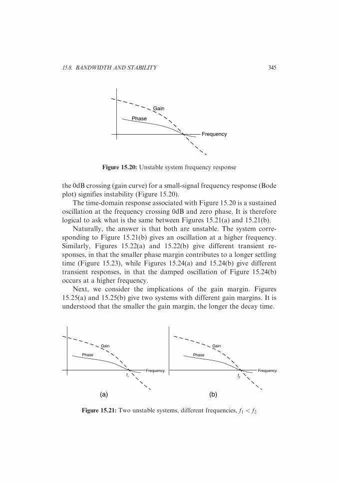
the 0dB crossing (gain curve) for a small-signal frequency response (Bode
plot) signifies instability (Figure 15.20).
The time-domain response associated with Figure 15.20 is a sustained
oscillation at the frequency crossing 0dB and zero phase. It is therefore
logical to ask what is the same between Figures 15.21(a) and 15.21(b).
Naturally, the answer is that both are unstable. The system corre-
sponding to Figure 15.21(b) gives an oscillation at a higher frequency.
Similarly, Figures 15.22(a) and 15.22(b) give different transient re-
sponses, in that the smaller phase margin contributes to a longer settling
time (Figure 15.23), while Figures 15.24(a) and 15.24(b) give different
transient responses, in that the damped oscillation of Figure 15.24(b)
occurs at a higher frequency.
Next, we consider the implications of the gain margin. Figures
15.25(a) and 15.25(b) give two systems with different gain margins. It is
understood that the smaller the gain margin, the longer the decay time.
Phase
Gain
Frequency
Figure 15.20: Unstable system frequency response
Phase
Gain
Frequencyf1
Phase
Gain
Frequencyf2
(a) (b)
Figure 15.21: Two unstable systems, different frequencies, f1 < f2
15.8. BANDWIDTH AND STABILITY 345
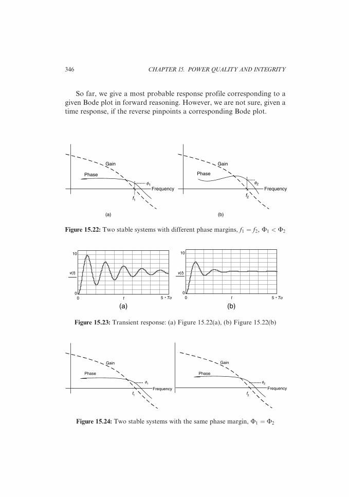
So far, we give a most probable response profile corresponding to a
given Bode plot in forward reasoning. However, we are not sure, given a
time response, if the reverse pinpoints a corresponding Bode plot.
Phase
Gain
Frequencyf2
Phase
Gain
Frequency
f1
(a) (b)
f1f2
Figure 15.22: Two stable systems with different phase margins, f1 ¼ f2, F1 < F2
10
0
v(t) v(t)
0 t
10
00 t
(a) (b)5 .To 5 .To
Figure 15.23: Transient response: (a) Figure 15.22(a), (b) Figure 15.22(b)
Phase
Gain
Frequencyf1
Phase
Gain
Frequencyf2
f2f1
Figure 15.24: Two stable systems with the same phase margin, F1 ¼ F2
346 CHAPTER 15. POWER QUALITY AND INTEGRITY
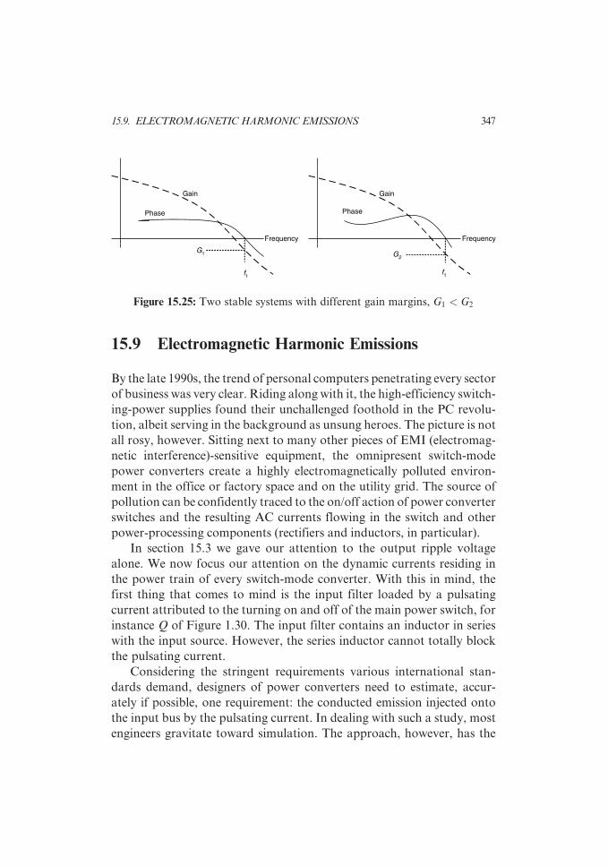
15.9 Electromagnetic Harmonic Emissions
By the late 1990s, the trend of personal computers penetrating every sector
of business was very clear. Riding along with it, the high-efficiency switch-
ing-power supplies found their unchallenged foothold in the PC revolu-
tion, albeit serving in the background as unsung heroes. The picture is not
all rosy, however. Sitting next to many other pieces of EMI (electromag-
netic interference)-sensitive equipment, the omnipresent switch-mode
power converters create a highly electromagnetically polluted environ-
ment in the office or factory space and on the utility grid. The source of
pollution can be confidently traced to the on/off action of power converter
switches and the resulting AC currents flowing in the switch and other
power-processing components (rectifiers and inductors, in particular).
In section 15.3 we gave our attention to the output ripple voltage
alone. We now focus our attention on the dynamic currents residing in
the power train of every switch-mode converter. With this in mind, the
first thing that comes to mind is the input filter loaded by a pulsating
current attributed to the turning on and off of the main power switch, for
instance Q of Figure 1.30. The input filter contains an inductor in series
with the input source. However, the series inductor cannot totally block
the pulsating current.
Considering the stringent requirements various international stan-
dards demand, designers of power converters need to estimate, accur-
ately if possible, one requirement: the conducted emission injected onto
the input bus by the pulsating current. In dealing with such a study, most
engineers gravitate toward simulation. The approach, however, has the
Phase
Gain
Frequency
f1
G1
Phase
Gain
Frequency
f1
G2
Figure 15.25: Two stable systems with different gain margins, G1 < G2
15.9. ELECTROMAGNETIC HARMONIC EMISSIONS 347

shortcoming discussed in Chapter 14. We instead address this specific
topic employing our old friend the accelerated steady state (refer to Figure
15.26). Again, two differential equation sets, dx=dt ¼ A .xþ B . u1 and
dx=dt ¼ A . xþ B . u2, are given, corresponding to two time segments,
0 < t < DT and DT < t < T , where
A ¼
� rL
L0 � 1
L
0 � 1
rdCd
1
rdCd
1
C
1
rdC� 1
rdC
26666664
37777775, B ¼
1
L0
0 0
0 � 1
C
26664
37775,
u1 ¼Vin
Ipk
� �, u2 ¼
Vin
0
� �(15:20)
Using MATLAB and the concept of the continuity of states, Appen-
dix G gives the input ripple current and the ripple voltage at the junction
of source resistance and input choke. The harmonic content of the ripple
voltage is also analyzed. The additional step yields a noise spectrum that
forms the basis of evaluation and approval for meeting various EMI
requirements and standards.
15.10 Power Quality
So far, we put in a great deal of effort to have an end product that is
robust in performance and reliable in quality, which is a totally separate
issue in its own right and not covered at all in this writing. So, what is the
Ipk
DT
(1−D)T
rd
LrL
Cd C
Vin
Figure 15.26: Input filter with pulsating current load
348 CHAPTER 15. POWER QUALITY AND INTEGRITY

measure of performance? Obviously, every user with neither understand-
ing of the workings of modern switch-mode power converters nor an idea
about the cost factors involved in making them will spell out a wish list as
shown in the following for a DC–DC converter:
Input line DC voltage range.
Output DC voltage range.
Output DC load range.
Output DC voltage-load regulation.
Output DC voltage-line regulation.
Output-load transient response (overshoot, undershoot, settling time).
Output-line transient response (overshoot, undershoot, settling time).
Output-overvoltage threshold.
Output-overload threshold.
The word wish may sound offensive. But, many of these performance
figures are indirectly mutually exclusive. One may be made acceptable at
the expense of others. Furthermore, the list does not include cost con-
siderations, which in general is not at the disposal of the designer. Size
and weight should also be part of the equation. And how about cooling,
the operating environment, electromagnetic interference, safety, reliabil-
ity, and other weird requirements? The point is that, once those consid-
erations are factored in, a proper specification for a power converter is
no longer a short list but a document containing many pages. Still,
electrical performance tops the list and is what electrical engineers expect
to optimize.
As discussed previously, steady-state output sensitivities against com-
ponents can be numerically evaluated. It was also understood that
steady-state output regulation is the cumulative result of component
tolerances and operating conditions. Given the ability of computing
sensitivity, the most sensitive components can be identified and their
sensitivities (volts/ohm, volts/unit change) quantified. At a higher cost,
steady-state regulation requirements can be met by tightening the toler-
ance of those offending components with high sensitivity; for example,
Vref and feedback resistors.
Next we tackle the time-varying aspect of the list. It was understood
from previous studies that high-speed response, or short settling time,
requires a wide bandwidth. Wide bandwidth, in turn, requires pole–
zero locations at high frequency as part of the closed-loop gain.
15.10. POWER QUALITY 349

High-frequency pole–zero locations are translated into small capacitor
values that set those pole–zero frequencies. The small capacitor values
run against the requirements of small overshoot under transient pertur-
bation. Stated differently, to support a high-speed transient load (high di/
dt) without large excursions off the regulation band, additional output
capacitors are generally called for. But large capacitor values degrade
bandwidth. Clearly, the transient performance of power converters does
not enjoy the advantage regulation possesses, in which performance
improvement is easily achievable by way of tightening component toler-
ances alone. Compromises among conflicting requirements are therefore
called for.
Worse yet, sensitivity figures of bandwidth, phase margin, gain mar-
gin, and overshoot against components are not readily available. Obtain-
ing symbolic solutions for those performance parameters is prohibitively
impossible. In theory, the frequency at which loop gain’s 0dB crossing
must first be found and expressed in explicit, closed form. With that, the
phase margin at that frequency also must be identified in closed form.
Phase margin sensitivity can then be evaluated. A similar process is
carried out for the gain margin. The difficulty, however, lies at the
juncture of finding 0dB crossing frequency and expressing it in symbolic
form. Without it, all bets are off. That being said, it is possible to do the
following given a loop gain T(s). Theoretically speaking, the 0dB crossing
frequency, fBW, can be obtained numerically:
T( j2p . fBW)j j � 1 ¼ 0 (15:21)
With fBW identified, the phase margin is given by ffT( j2p . fBW, . . . , Rx)
and its sensitivity against Rx is @ffT( j2pfBW, . . . , Rx)=@Rx. Similarly, the
gain margin and sensitivity can be obtained by first finding the zero-
phase frequency, f0, with the imaginary part of the loop gain set to zero:
Im[T( j2p . f0)] ¼ 0 (15:22)
The gain margin, jT( j2p . f0, . . . , Rx)j, and sensitivity,
@ffT( j2pf0, . . . , Rx)=@Rx, follows. However, another difficulty arises.
Whatever improvement is made for the phase margin based on phase
margin sensitivity figures may work against the gain margin, or vice
versa. In essence, the uncertainty is recognized. But, we are awkwardly
350 CHAPTER 15. POWER QUALITY AND INTEGRITY

equipped to provide an answer. This unpleasant situation spills over to
our inability to control overshoot. Not only are we unable to formulate
the closed-loop transient overshoot in symbolic form, we are also unable
to correlate the response with bandwidth and stability.
In summary, we understand what constitutes high quality for power
converter performance under normal and abnormal operations, but we
are awfully short of means, even if cost is not a concern. At least we
understand at a qualitative level how things work. This is fertile ground
where a lot of innovations are waiting to be made.
15.10. POWER QUALITY 351

This page intentionally left blank

Appendix A
Additional Filtering for ForwardConverter Current Sensing
The equivalent circuit for the current sensor with additional filter (Rf and
Cf ) is depicted in Figure 1.30. For the steady-state analysis, the driving
current source is placed in (aþ bt) form by rewriting equation (1.50). It is
understood that
a ¼ .1
ni
Ns
Np
Io �(Vo þ VD)(1�D)
2L . fs
� �(A:1)
b ¼ 1
ni
Ns
Np
Ns
Np
Vin � VD � Vo
Lþ Vin
Lp
0BB@
1CCA (A:2)
Given an unknown initial voltage, VF, the output voltage in Laplace
transformation form is
V (s) ¼ VF
sþ 1t
þ k . a .1
s sþ 1t
� �þ k . b .1
s2 sþ 1t
� � (A:3)
353
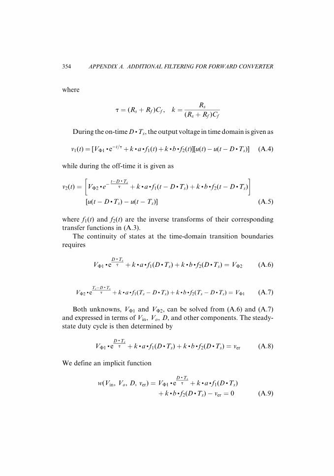
where
t ¼ (Rs þ Rf )Cf , k ¼ Rs
(Rs þ Rf )Cf
During the on-timeD . Ts, the output voltage in time domain is given as
v1(t)¼ [VF1 . e�t=tþ k . a . f1(t)þ k . b . f2(t)][u(t)� u(t�D . Ts)] (A:4)
while during the off-time it is given as
v2(t) ¼ VF2 . e�t�D . Ts
t þ k . a . f1(t�D . Ts)þ k . b . f2(t�D . Ts)
� �[u(t�D . Ts)� u(t� Ts)] (A:5)
where f1(t) and f2(t) are the inverse transforms of their corresponding
transfer functions in (A.3).
The continuity of states at the time-domain transition boundaries
requires
VF1 . eD . Ts
t þ k . a . f1(D .Ts)þ k . b . f2(D . Ts) ¼ VF2 (A:6)
VF2 . eTs�D . Ts
t þ k . a . f1(Ts �D . Ts)þ k . b . f2(Ts �D . Ts) ¼ VF1 (A:7)
Both unknowns, VF1 and VF2, can be solved from (A.6) and (A.7)
and expressed in terms of Vin, Vo, D, and other components. The steady-
state duty cycle is then determined by
VF1 . eD . Ts
t þ k . a . f1(D . Ts)þ k .b . f2(D . Ts) ¼ ver (A:8)
We define an implicit function
w(Vin, Vo, D, ver) ¼ VF1 . eD . Ts
t þ k . a . f1(D .Ts)
þ k . b . f2(D . Ts)� ver ¼ 0 (A:9)
354 APPENDIX A. ADDITIONAL FILTERING FOR FORWARD CONVERTER

Appendix B
MathCAD Listing,Steady-State Output forFigure 1.42
DC–DC converter output filter, Steady-state output, Laplace transform
approach:
Np: ¼ 19
Ns: ¼ 12
Vbus: ¼ 28
Expected output voltage:
Vo: ¼ 5.3
Load:
Io: ¼ 2.5
RL:¼ Vo
Io
Output filter:
L:¼ 102 . 10�6
355

C:¼ 100 . 10�6
rL:¼ 0:005
rC: ¼ 0.01
Rp:¼ rC . RL
rCþRL
k:¼ RL
rCþRL
Rectifier drop
VD: ¼ 0.5
Auxilary equation
vo(t) ¼ Rp . i(t)þ k .v(t)
Expected switching duty cycle
Du:¼ Voþ VDþ rL . Io
Ns
Np
� �. Vbus
Switching frequency
fs:¼ 125 . 103
Ts:¼ 1
fs
voL
rLrC
C
RLv
Vbus
Ns
Np−VD
−VD
356 APPENDIX B. MATHCAD LISTING, STEADY-STATE OUTPUT

D(s): ¼ s2 þ �1
(rC .C).kþ 1
(rC . C)þ 1
L.Rpþ 1
L. rL
� �. s
þ 1
L.
rL
(rC . C)� 1
L.
rL
(rC . C). kþ 1
L.
Rp
(rC . C)
F1(s):¼sþ 1� k
rC . CD(s)
F2(s):¼ �k
LD(s)
F3(s):¼
Ns
Np. Vbus� VD
� �. 1
L. sþ 1� k
rC .C
� �s . D(s)
G1(s):¼Rp
rC . CD(s)
G2(s):¼sþ rLþRp
LD(s)
G3(s):¼
Ns
Np. Vbus� VD
� �.1
L.
Rp
rC .C
s . D(s)
F4(s):¼�VD .
1
L. sþ 1� k
rC . C
� �s . D(s)
G4(s):¼�VD .
1
L.
Rp
rC . Cs .D(s)
APPENDIX B. MATHCAD LISTING, STEADY-STATE OUTPUT 357

f1(t) :¼ invlaplace(F1(s), s, t) float, 3!
f2(t) :¼ invlaplace(F2(s), s, t) float, 3!
f3(t) :¼ invlaplace(F3(s), s, t) float, 3!
f4(t) :¼ invlaplace(F4(s), s, t) float, 3!
g1(t) :¼ invlaplace(G1(s), s, t) float, 3!
g2(t) :¼ invlaplace(G2(s), s, t) float, 3!
g3(t) :¼ invlaplace(G3(s), s, t) float, 3!
g4(t) :¼ invlaplace(G4(s), s, t) float, 3!
I :¼ identity (2)
A1 :¼ f1(Du . Ts) f2(Du . Ts)
g1(Du . Ts) g2(Du . Ts)
� �
B1 :¼ f3(Du . Ts)
g3(Du . Ts)
� �
A2 :¼ f1[(1�Du) . Ts] f2[(1�Du) . Ts]
g1[(1�Du) .Ts] g2[(1�Du) . Ts]
� �
B2 :¼ f4[(1�Du) . Ts]
g4[(1�Du) . Ts]
� �
On starting:
X1 :¼ (I�A2 . A1)�1 . (A2 . B1þ B2)
Off starting:
X2 :¼ A1 . X1þ B1
358 APPENDIX B. MATHCAD LISTING, STEADY-STATE OUTPUT

Inductor current:
i(t) :¼ X1T .f 1(t)
f 2(t)
� �þ f 3(t)
� �. F(t)�F(t�Du . Ts)ð Þ . . .
þ X2T .f 1(t�Du . Ts)
f 2(t�Du . Ts)
� �þ f 4(t�Du . Ts)
� �. F(t�Du . Ts)�F(t� Ts)ð Þ
Output voltage:
v(t) :¼ (X1)T .g1(t)
g2(t)
� �þ g3(t)
� �. F(t)�F(t�Du .Ts)ð Þ . . .
þ (X2)T .g1(t�Du . Ts)
g2(t�Du . Ts)
� �þ g4(t�Du . Ts)
� �. F(t�Du . Ts)�F(t� Ts)ð Þ
vo(t) :¼ Rp . i(t)þ k . v(t)
v(t) :¼X4
n¼0
vo(t� n . Ts)0
iL(t) :¼X4
n¼0
i(t� n . Ts)0
t :¼ 0,0:001 . Ts::5 . Ts
APPENDIX B. MATHCAD LISTING, STEADY-STATE OUTPUT 359

This page intentionally left blank

Appendix C
MATLAB Listing, Steady-StateOutput for Figure 1.42
Np¼19;
Ns¼12;
L¼102*10^ � 6;
rL¼0.005;
rc¼0.01;
C¼100*10^ � 6;
Vbus¼28;
VD¼0.5;
Vo¼5.3;
Io¼2.5;
RL¼Vo/Io;
fs¼125*10^3;
T¼1/fs;
k¼RL/(RLþrc);
361

Rp¼(rc*RL)/(rcþRL);
Du¼(VoþVDþIo*rL)/((Ns/Np)*Vbus);
vg1¼(Ns/Np)*Vbus-VD;
vg2¼-VD;
a11¼-(rLþRp)/L;
a12¼-k/L;
a21¼Rp/(rc*C);
a22¼-(1-k)/(rc*C);
A¼[ a11 a12; a21 a22 ];
B¼[1/L; 0];
A1¼A*Du*T;
A2¼A*(1-Du)*T;
I¼eye(2,2);
X1¼inv(I-expm(A2)*expm(A1))*(-expm(A2)*inv(A)*
(I-expm(A1))*B*vg1-inv(A)*(I-expm(A2))*B*vg2)
X2¼expm(A1)*X1-inv(A)*(I-expm(A1))*B*vg1
Y1¼[ ];
for t¼0:T/100:Du*T;
Y1¼[Y1 expm(A*t)*X1-inv(A)*(I-expm(A*t))*B*vg1];
end
Y2¼[ ];
for t¼Du*T:T/100:T;
Y2¼[Y2expm(A*(t-Du*T))*X2-inv(A)*(I-expm(A*
(t-Du*T)))*B*vg2];
end
362 APPENDIX C. MATLAB LISTING, STEADY-STATE OUTPUT

Time¼0:T/100:T;
Current¼[Y1(1,:) Y2(1,:)];
Voltage¼[Y1(2,:) Y2(2,:)];
Output¼Current*Rpþk*Voltage;
figure(1)
plot(Time,Current);
figure(2)
plot(Time,Output);
APPENDIX C. MATLAB LISTING, STEADY-STATE OUTPUT 363

This page intentionally left blank

Appendix D
MathCAD Listing,Steady-State Current-SensingOutput
+
−+
−
Rl
Ri
RfCfz
Cfp
iL
Ts
Vm
Vc +
−
Vref
Vo
Powerswitch
Driver
Input
kf
Vg
D
L
Vb
Vi
Average current loop
K:¼ 103
u:¼ 10�6
m:¼ 10�3
365

n:¼ 10�9
p:¼ 10�12
Fs:¼ 50 .K
Vg:¼ 14
Vo:¼ 5
L:¼ 37:5 .u
C:¼ 380 . u
Rc:¼ 20 . m
Ri:¼ 0:1
R1:¼ 2:2 . K
Rf :¼ 30:5 .K
Cfz:¼ 5:8 . n
Cfp:¼ 220 . p
T:¼ 1
Fs
d:¼ Vo
Vg
Load resistance:
R:¼1
Control voltage:
Vc:¼ 0:5
di:¼ Vg� Vo
L. d .T
366 APPENDIX D. MATHCAD, STEADY-STATE CURRENT-SENSING OUTPUT

t1:¼ Cfp .R1 .Rf
R1þRf
IL:¼ Vo
R
Ib:¼ IL� di
2
t2:¼ Rf . Cfp
t3:¼ Rl .Cfp
t4:¼ Rf . Cfz
Sn:¼ Vg � Vo
L
Let
ton:¼ d .T
tof :¼ (1� d) .T
Current slope alone:
vp:¼ 1
t4þ 1
t2
vz:¼ 1
t4
vx:¼ 1
t1þ 1
t4
vy:¼ 1
t3
vh:¼ 1
t2
APPENDIX D. MATHCAD, STEADY-STATE CURRENT-SENSING OUTPUT 367

a1:¼ Vg � Vo
L . Ib
B1:¼ a1
vp
A1:¼ 1
vp. (1� B1)
D1:¼ �A1
b1:¼ Ri . Ib
t3. A1þ B1 . tonþD1 . e�vp . ton� �
� vx
vp. 1� e�vp . ton� �
. Vc
a11:¼ e�vp . ton
a12:¼ �1
a2:¼ �Vo
L . (Ibþ di)
B2:¼ a2
vp
A2:¼ 1
vp. (1� B2)
D2:¼ �A2
b2:¼ Ri . (Ibþ di)
t3. A2þ B2 . tof þD2 . e�vp . tof� �
� vx
vp. 1� e�vp . tof� �
. Vc
a21:¼ �1
a22:¼ e�vp . tof
vbx:¼
b1 a12
b2 a22
��������
a11 a12
a21 a22
��������
368 APPENDIX D. MATHCAD, STEADY-STATE CURRENT-SENSING OUTPUT

vby:¼
a11 b1
a21 b2
��������
a11 a12
a21 a22
��������
vb1(t):¼ vbx . e�vp . t þ Vc .vx
vp. 1� e�vp . t� �
�Ri . Ib
t3
. A1þ B1 . tþD1 . e�vp . tð Þ
vb2(t):¼ vbye�vp(t�ton) þ Vc .vx
vp. 1� e�vp . (t�ton)� �
�Ri(Ibþ d)
t3
. A2þ B2(t� ton)þD2e�vp . (t�ton)� �
Voltage at the Rf–Cfz node:
vb(t):¼ vb1(t) . F(t)�F(t� ton)ð Þ þ vb2(t) . F(t� ton)�F(t� T)ð Þ
t:¼ 0, 0:002 . T::T
Idc:¼ 1
Rf . T.
ðT
0
(Vc� vb(t) )dt
� �
The compensator output:
vm(t):¼ vb(t)� 1
Cfz.
ðt
0
Vc� vb(t)
Rf� Idc
� dt
The source function during ton:
v1(t):¼ Ri . (Ibþ Sn . t)
during tof:
v2(t):¼ Ri . Ibþ di� Vo
L. (t� d .T)
� �
vi(t):¼ v1(t) . F(t)�F(t� d .T)ð Þ þ v2(t) . F(t� d . T)�F(t� T)ð Þ
APPENDIX D. MATHCAD, STEADY-STATE CURRENT-SENSING OUTPUT 369

Slope of vm(t) at t ¼ ton according to the preceding calculation:
Sm(t):¼ Vc
t1� v1(t)
t3� vb(t)
t2
jSm(ton)j ¼ 1:714� 105
Slope of vm(ton) according to (2) of paper:
Sn . Ri ¼ 2:4� 104
vi:¼ 1
R1 . (Cfpþ Cfz)
Sn0:¼ vi . Sn . d . Tþ 1
vz� 1
vp
� . 1� e�vp . d . T� �� �
.Ri
Sn0 ¼ 2:195� 105
Sn0
Sn . Ri¼ 9:145
jSm(ton)jSn . Ri
¼ 7:143
Finding external ramp waveform:
Se:¼ 0:15 . 106
vx:¼ 1
Given
Se . ton ¼ vm(ton)
se:¼ Find(Se)
se ¼ 6:647� 104
ve(t): ¼ (se . t) . F(t)�F(t� 0:99T)ð Þ
þ se .0:99T � se .0:99T
0:01T. (t� :99T)
� �. (F(t� :99T)�F(t� T)Þ
370 APPENDIX D. MATHCAD, STEADY-STATE CURRENT-SENSING OUTPUT

Appendix E
MATLAB Listing, ConverterSimulation
N1¼19;
N2¼12;
Lm¼1150*N1^2*10^�9;
rw¼0.1;
Ron¼0.2;
Roff¼10^7;
L1¼102*10^�6;
rL1¼0.005;
Vg¼28;
L2¼385*10^�6;
rL2¼0.077;
RL¼5;
fs¼125*10^3;
T¼1/fs;
371

C9¼100*10^�6;
rc1¼0.01;
VD¼0.5;
Vref¼2.5;
A¼10^5;
R35¼9.76*10^3;
R70¼11.11*10^3;
kf¼R35/(R35þR70);
Rp¼(rc1*RL)/(rc1þRL);
k¼RL/(rc1þRL);
R12¼2*10^3;
R45¼24.3*10^3;
C37¼560*10^�12;
C29¼2200*10^�12;
R43¼10*10^3;
Vbe¼0.7;
R20¼5.11*10^3;
R33¼2.94*10^3;
hfe¼150;
R19¼5.11*10^3;
R31¼6.65*10^3;
R39¼33.2*10^3;
C39¼560*10^�12;
C7¼60*10^�6;
rc2¼2.61;
372 APPENDIX E. MATLAB LISTING, CONVERTER SIMULATION

C8¼60*10^�6;
Rx¼50*10^6;
Du¼0.328;
a11¼�(rL1þRp)/L1�((rw þ Ron)*(N2/N1)^2)/L1;
a12¼�k/L1;
a18¼N2/(L1*N1);
a19¼�N2*(rwþRon)/(L1*N1);
a21¼Rp/(rc1*C9);
a22¼(k�1)/(rc1*C9);
a31¼�(A*kf*Rp)/((1þA)*R12*C37);
a32¼�(A*kf*k)/((1þA)*R12*C37);
a33¼�A/((1þA)*R45*C37)�1/(R45*C29);
a34¼(A/((1þA)*C37))*(1/R12þ1/R45þ(1þA)/Rx)þ1/(R45*C29);
a41¼(kf*Rp)/((1þA)*R12*C37);
a42¼(kf*k)/((1þA)*R12*C37);
a43¼1/((1þA)*R45*C37);
a44¼�(1/((1þA)*C37))*(1/R12þ1/R45þ(1þA)/Rx);
Kb2¼(A*R20)/(R20*R43þ(1þhfe)*R33*(R20þR43));
a54¼((hfe*R31*R19/(R31þR19))/((1þA)*R31*C39))*Kb2;
a55¼(R19/((R19þR31)*R31)�1/R31�(1þA)/R39)/ (1þA)*C39);
a66¼�rL2/L2;
a68¼�1/L2;
a77¼�1/(rc2*C7);
a78¼1/(rc2*C7);
a81¼�N2/(N1*C8);
APPENDIX E. MATLAB LISTING, CONVERTER SIMULATION 373

a86¼1/C8;
a87¼1/(rc2*C8);
a88¼�a87;
a89¼�a86;
a91¼�N2*(rwþRon)/(N1*Lm);
a98¼1/Lm;
a99¼�(rwþRon)/Lm;
A1 ¼ [ a11 a12 0 0 0 0 0 a18 a19; a21 a22 0 0 0 0 0 0 0; a31 a32 a33 a34 0 0
0 0 0;a41 a42 a43 a44 0 0 0 0 0;0 0 0 a54 a55 0 0 0 0;0 0 0 0 0 a66 0
a68 0;0 0 0 0 0 0 a77 a78 0;a81 0 0 0 0 a86 a87 a88 a89;a91 0 0 0 0 0 0
a98 a99];
b1¼�VD/L1;
b3¼�A^2*Vref/((1þA)*Rx*C37);
b4¼A*Vref/((1þA)*Rx*C37);
Kb1¼(�R43*(10�VD)þ(R20þR43)*(10�Vbe)�A*R20*Vref)/
(R20*R43þ(1þhfe)*R33*(R20þR43));
b5¼((hfe*R31*R19/(R31þR19))/((1þA)*R31*C39))*Kb1þ(A*Vref)/((1
þA)*R39*C39);
b6¼Vg/L2;
B¼[b1;0;b3;b4;b5;b6;0;0;0];
d11¼�(rL1þRp)/L1;
d99¼�(rwþRoff)/Lm;
A2 ¼ [ d11 a12 0 0 0 0 0 0 0; a21 a22 0 0 0 0 0 0 0; a31 a32 a33 a34 0 0 0 0
0;a41 a42 a43 a44 0 0 0 0 0;0 0 0 a54 a55 0 0 0 0;0 0 0 0 0 a66 0 a68
0;0 0 0 0 0 0 a77 a78 0;0 0 0 0 0 a86 a87 a88 a89;0 0 0 0 0 0 0 a98
d99];
A3¼A1*Du*T;
A4¼A2*(1�Du)*T;
374 APPENDIX E. MATLAB LISTING, CONVERTER SIMULATION

I¼eye(9,9);
X1¼inv(I�expm(A4)*expm(A3))*(�expm(A4)*inv(A1)*(I�expm(A3))*B�inv(A2)*(I�expm(A4))*B)
X2¼expm(A3)*X1�inv(A1)*(I�expm(A3))*B
Y1¼[ ];
for t¼0:T/100:Du*T;
Y1¼[Y1 expm(A1*t)*X1�inv(A1)*(I�expm(A1*t))*B];
end
Y2¼[ ];
for t¼Du*TþT/100:T/100:T;
Y2¼[Y2 expm(A2*(t�Du*T))*X2�inv(A2)*(I�expm(A2*
(t�Du*T)))*B];
end
%output inductor current
Current¼[Y1(1,:) Y2(1,:)];
iL¼repmat(Current,[1 5]);
%ideal cap
Voltage¼[Y1(2,:) Y2(2,:)];
%output voltage
Output¼Rp*Currentþk*Voltage;
vo¼repmat(Output,[1 5]);
%transformer secondary current
%switch current
%C29 node
VC29¼[Y1(3,:) Y2(3,:)];
v2¼repmat(VC29,[1 5]);
APPENDIX E. MATLAB LISTING, CONVERTER SIMULATION 375

%error amp inverting node
Vinvert¼[Y1(4,:) Y2(4,:)];
vn¼repmat(Vinvert,[1 5]);
%pwm inverting node
Vpwminv¼[Y1(5,:) Y2(5,:)];
vn2¼repmat(Vpwminv,[1 5]);
%input current
Iin¼[Y1(6,:) Y2(6,:)];
i2¼repmat(Iin,[1 5]);
%input filter cap one
VC7¼[Y1(7,:) Y2(7,:)];
v3¼repmat(VC7,[1 5]);
%primary winding voltage
Vpri¼[Y1(8,:) Y2(8,:)];
v4¼repmat(Vpri,[1 5]);
%mag current
imag¼[Y1(9,:) Y2(9,:)];
im¼repmat(imag,[1 5]);
%plotting
Time ¼ 0:T/100:5*T�T/100;
figure(1)
plot(Time,iL);
figure(2)
plot(Time,vo);
figure(3)
376 APPENDIX E. MATLAB LISTING, CONVERTER SIMULATION

plot(Time,v2);
figure(4)
plot(Time,vn);
figure(5)
plot(Time,vn2);
figure(6)
plot(Time,i2);
figure(7)
plot(Time,v3);
figure(8)
plot(Time,v4);
figure(9)
plot(Time,im);
APPENDIX E. MATLAB LISTING, CONVERTER SIMULATION 377

This page intentionally left blank

Appendix F
Capacitor and Inductor
Capacitor
The mathematical equation governing the capacitor behavior is given by
ic ¼ Cdvc
dt
in differential form. It certainly can be placed in integral form:
vC ¼ v0 þ1
C
ðt
0
iC(t)dt
Both equations give quite a few important insights:
1. When ic ¼ 0, dvc=dt ¼ 0. The latter signifies analytically the existence
of extreme values for variable vc at the particular moment. In other
words, vc max or vc min occurs at the zero crossing of the capacitor
current; figure follows:
vC
iC0
0
379

2. Being the integral of the other variable ic (integrand), capacitor volt-
age lags behind the corresponding current.
3. The second fact also implies that the capacitor does not take in direct
current for long. If it does, the terminal voltage exceeds its maximum
rating and destroys its dielectric material.
4. Direct voltage does not contribute to the capacitor current. The
capacitor blocks direct current.
5. The capacitor can be biased with a direct voltage.
Inductor
The mathematical equation governing the inductor behavior is given by
vL ¼ LdiL
dt
in differential form. It certainly can be placed in integral form:
iL ¼ i0 þ1
L
ðt
0
vL(t)dt
Both equations give quite a few important insights:
1. When vL ¼ 0, diL=dt ¼ 0. The latter signifies analytically the existence
of extreme values for variable iL at the particular moment. In other
words, iL max or iL min occurs at the zero crossing of the inductor
voltage; figure follows:
iL
vL
0
0
2. Being the integral of the other variable vL (integrand), the inductor
current lags behind the corresponding voltage.
3. The second fact also implies that the inductor does not take in direct
voltage for long. If it does, the terminal current exceeds saturation.
4. Direct current does not contribute to the inductor voltage.
5. The inductor can be biased with a direct current.
380 APPENDIX F. CAPACITOR AND INDUCTOR

Appendix G
MATLAB Listing for an InputFilter with a Pulsating Load
N1¼19;
N2¼12;
L¼385*10^�6;
rL¼0.005;
rd¼2.6;
Cd¼60*10^�6;
C¼60*10^�6;
Vin¼28;
Vo¼5.3;
VD¼0.5;
Io¼2.5;
Ipk¼(N2*Io)/N1;
fs¼125*10^3;
T¼1/fs;
381

Du¼(VoþVDþIo*rL)/((N2/N1)*Vin);
a11¼-rL/L;
a12¼0;
a13¼�1/L;
a21¼0;
a22¼�1/(rd*Cd);
a23¼�a22;
a31¼1/C;
a32¼1/(rd*C);
a33¼�a32;
A¼[ a11 a12 a13; a21 a22 a23; a31 a32 a33];
B¼[1/L 0; 0 0; 0 �1/C];
A1¼A*Du*T;
A2¼A*(1-Du)*T;
I¼eye(3,3);
u1¼[Vin; Ipk];
u2¼[Vin; 0];
X1¼inv(expm(A*T)-I)*(expm(A2)*inv(A)*(I-expm(A1))*B*u1þinv(A)*(I-expm(A2))*B*u2)
X2¼expm(A1)*X1-inv(A)*(I-expm(A1))*B*u1
Y1¼[ ];
for t¼0:T/100:Du*T;
Y1¼[Y1 expm(A*t)*X1-inv(A)*(I-expm(A*t))*B*u1];
end
Y2¼[ ];
for t¼Du*TþT/100:T/100:T;
382 APPENDIX G. MATLAB LISTING FOR AN INPUT FILTER

Y2¼[Y2 expm(A*(t-Du*T))*X2-inv(A)*(I-expm(A*(t-Du*T)))*B*u2];
end
Current¼[Y1(1,:) Y2(1,:)];
Voltage¼[Y1(3,:) Y2(3,:)];
iL¼repmat(Current,[1 5]);
vo¼repmat(Voltage,[1 5]);
Time¼0:T/100:5*T-T/100;
figure(1)
plot(Time,iL);
figure(2)
plot(Time,vo);
APPENDIX G. MATLAB LISTING FOR AN INPUT FILTER 383

This page intentionally left blank

References
[1] R.D. Middlebrook and Slobodan Cuk. Advances in Switched-Mode Power
Conversion. Pasadena, CA: TESLco.
[2] Keng C. Wu. Pulse Width Modulated DC-DC Converters. London: Chap-
man & Hall, 1997.
[3] Wei Tang and Fred C. Lee. ‘‘Small-Signal Modeling of Average Current-
Mode Control.’’ IEEE Trans. on Power Electronics. PE-8, no. 2 (April
1993): 112.
[4] Texas Instruments. ‘‘Phase Shifted, Zero Voltage Transition Design Con-
siderations and the UC3875 PWM Controller.’’ (Unitrode) Application
Note, U-136A.
[5] Kwang-hwa Liu, Ramesh Orugnati, and Fred C. Lee. ‘‘Quasi-Resonant
Converters—Topologies and Characteristics.’’ IEEE Trans. on Power Elec-
tronics PE-2, no. 1 (January 1987): 62.
[6] Marian K. Kazimierczuk. ‘‘Class-E DC/DC Converters with a Capacitive
Impedance Inverter.’’ IEEE Trans. on Industrial Electronics. IE-36, no. 3
(August 1989): 425.
[7] Marian K. Kazimierczuk. ‘‘Class-E Amplifiers with an Inductive Imped-
ance Inverter.’’ IEEE Trans. on Industrial Electronics. IE-37, no. 2 (April
1990): 160.
[8] Nathan O. Sokal and Alan D. Sokal. ‘‘Class E-A New Class of High-
Efficiency Tuned Single-Ended Switching Power Amplifiers.’’ IEEE Journal
of Solid-State Circuits. SC-10, no. 3 (June 1975).
[9] Jacek J. Jozwik and Marian K. Kazimierczuk. ‘‘Analysis and Design of
Class-E2 DC/DC.’’ IEEE Trans. on Industrial Electronics. IE-37, no. 2
(April 1990): 173.
385

[10] Keng C. Wu. Transistor Circuits for Spacecraft Power System. Norwell,
MA: Kluwer Academic Publishers, 2002.
[11] Ron-Jie Tu and Chern-Lin Chen. ‘‘A New Space-Vector-Modulated Con-
trol for a Unidirectional Three-Phase Switch-Mode Rectifier.’’ IEEE Trans.
on Industrial Electronics. IE-45, no. 2 (April 1998): 256.
[12] K. Mark Smith and Keyue Ma Smedley. ‘‘Lossless Passive Soft-Switching
Methods for Inverters and Amplifiers.’’ IEEE Trans. on Power Electronics.
PE-15, no. 1 (January 2000): 164.
386 REFERENCES

Index
amplifier
compensation, 189, 190, 242
error, 10, 17, 36, 38, 72, 113, 125,
139, 140, 142, 165, 174, 184,
186, 187, 220, 242, 243, 247,
249, 276, 278, 282, 288, 293,
296, 298, 313
summing, 71, 72
transconductance, 40, 137
angular displacement, 205
average load power, 175
average value, 5, 21, 57
Baker clamp, 253
bidirectional switches, 229
Bode plot, 346
Boolean algebra, 234
boost
inductor, 149, 214, 225, 229
PFC, 207, 208
ratio, 212, 214
boundary conditions, 270, 273
Cayley-Hamilton theorem, 47
CCM, 1, 2, 4, 6, 7, 11, 12, 14, 15, 16,
18–26, 51, 52, 53, 61, 63, 64,
65, 67, 119–123, 125, 126,
129–133, 149–153, 156, 210,
214, 215, 216
charge balance, 133
clamping diode, 100, 259, 260
closed-loop output, 12, 13, 22, 35,
65, 186, 331
component
sensitivities, 139
tolerance, 329, 330, 350
conducted
emission, 347
susceptibility, 19, 25, 125, 129,
132, 146, 147
continuity of state, 27, 46, 55, 56,
70, 103, 110, 181, 265, 269,
272, 313, 326, 333, 348, 354
continuous conduction mode, 1,
100
control
average current-mode, 67, 68
base current, 255
current-mode, 19, 20, 21, 25,
49, 50, 51, 52, 120, 127, 136,
149, 288, 306
forward current, 217
nonlinear, 14
voltage-mode, 9, 11, 22, 119, 120,
149, 292, 293, 299, 301
control-loop gain, 334
conversion efficiency, 208, 215
converter
buck, 1, 13, 17, 18, 23, 76, 83
class-E power, 173
flyback, 119, 120, 122, 124, 125,
127, 149, 167
387

converter (continued)
full-bridge, 83, 84,
336, 338
quasi-resonant, 165
voltage-to-current, 36, 37, 38, 39,
140, 142, 143
core
ferrous, 20
reset, 49
saturation, 49
corner frequencies, 239
cosine series, 336
critical inductance, 6, 7, 100, 120,
123, 149
critical inductor value, 6
crossover frequency, 190, 243, 245
current
bias, 10, 244, 246
command, 109, 231
-fed, 95, 108, 109
feedback voltage, 111
forward, 188, 217
free-wheeling, 85
inrush, 221
instantaneous switch, 20
limit, 50, 221, 262
limiter, 221
limiting, 262
nonpulsating input, 282
pulsating, 4, 95, 98, 160, 262, 347,
348
pulsating inductor, 210
resonant, 159, 160, 198, 199
ripple, 7, 68, 93, 108, 135, 215,
348
sensor, 110, 113, 219, 231, 353
shaping, 217
sharing, 204, 217, 219, 262
transformer, 20, 22, 54, 110, 222,
254, 262
zero-, 157, 159, 168, 171
current-sharing controller, 219, 220
damped oscillation, 343, 345
damping, 27, 30, 33, 174, 187, 188,
201, 293, 294, 295
capacitor, 27, 30, 33
critical, 27
effect, 174, 187
load-dependent, 27
resistor, 33, 187
series, 187
Darlington driver, 250, 255
DCM, 1, 2, 5, 6, 7, 13, 14, 19, 20,
21, 51–54, 57, 58, 59, 61, 62,
65, 119, 120, 121, 123,
124–129, 132, 133, 136, 138,
140, 142, 144, 146, 148, 149,
150, 151, 153–156, 210, 212,
214, 215
dependent sources, 15
diode
ideal, 3
rectifier, 3, 35
double pole, 241
double zero, 241, 245
drive
base, 250, 251, 252, 254
floating, 252, 255
drivers
MOSFET, 249
duty cycle
open-loop, 11, 12, 22, 57, 71, 98,
105, 121, 122
variable, 3
duty limit, 278
duty-cycle clamping, 274
dynamic resistances, 188
electromagnetic interference, 83,
203, 349
EMI, 207, 347, 348
388 INDEX

end states, 32
energy storage inductor, 119,
129, 206
external oscillator, 55,
126, 292
feedback
average current, 109
current, 39, 50, 51, 67, 111, 127,
142, 151, 153, 261, 262, 263,
264, 306
path, 12, 145, 294
ratio, 17, 113, 184, 189, 282, 288,
330
feedforward, 128,
145, 146
field programmable gate array, 236
filter
LC, 2, 27
line, 15
line input, 124, 126, 143
loaded output, 17
first-order differential equations,
268, 282
flux
conservation, 1, 5
imbalance, 49
flyback phase, 120
form
determinant, 59
discrete, 291, 293,
296
explicit, 23, 58, 122
polynomial, 46, 47, 77
forward bias, 219
Fourier coefficients, 338
frequency, 3-db roll-off, 9
frequency domain, 178, 191
full-wave rectifier, 110, 187, 221,
267, 268, 271
gain
and bandwidth, 8
closed-loop, 349
coefficients, 24
compensation, 242
control-loop, 334
deficiency, 243, 245
loop, 18, 19, 25, 36, 40–43, 75,
125, 126, 131, 136, 143, 144,
149, 153, 155, 167, 174, 187,
242, 248, 282, 288, 289, 290,
350
low frequency, 9
margin, 345, 347, 350
modulator, 243, 245
open-loop, 8, 9, 36, 128, 140, 166,
186
PWM, 11, 18, 39, 40, 130, 154,
282, 287
harmonic contents, 83, 203, 337
hysteretic comparator, 34, 137
ideal rectifiers, 1
impedance interaction factor, 41
implicit function, 4, 12, 14, 35, 65,
72, 73, 74, 75, 131, 152, 165,
331, 354
initial tolerance, 329, 330
inner current loop, 25, 60
input perturbation, 19, 145
input-to-output transfer function,
139
isolation barrier, 262
Jacobian determinant, 13, 73, 74,
166, 331
junction diodes, 188
INDEX 389

Laplace transformations, 45
leakage inductance, 158, 159
linear models, 14
linear system analysis, 14
load
current sharing, 217, 219
effective, 200
lines, 259
reflection, 200
regulation, 139, 166, 349
sensitivity, 13
sharing, 217
loop partition, 58, 237
losses
diode, 5
primary side, 4
saturation, 259
secondary side, 4
losses
series, 1, 4
series resistive, 41
switching, 160, 171, 259
magnetic
circuit breaker, 222
isolation, 143
magnetizing inductance, 113, 200,
201
matrix exponentials, 46, 77, 80, 81,
326
mode
discontinuous conduction, 50
freewheeling, 85
nonoverlapping, 95
overlapping, 95, 100
peak current-, 19, 21, 33, 67, 120,
128, 129, 130, 131, 311, 314, 325
model
average, 333
canonical, 124, 126, 143
cycle-by-cycle, 333
state-space averaged, 39, 115
noise spectrum, 348
nonlinear magnetic cores, 292
operational amplifiers, 7
opto-coupler, 263
output sensitivity, 58, 73, 166, 186,
330, 334
parallel operation, 204
parasitic capacitance, 187
parasitic elements, 39, 332, 334
partial derivative, 18, 24, 73, 330
PFC, 203, 204, 206–209, 217, 218,
220–226, 228, 230, 232, 234
phase
boost, 190, 239, 241, 242, 243,
245
delay, 21
margin, 190, 242, 243, 245, 247,
298, 344, 345, 346, 350
modulator, 243, 245
nonconducting, 272
resonant, 159
transient, 313, 333
pole
first-order, 9
lagging, 21
power
dissipation, 33, 92, 93, 157, 219,
259
factor, 203, 205, 271
transfer, 200, 203
power stage, 1, 3, 7, 12, 13, 14, 39,
41, 50, 51, 53, 57, 58, 59, 63, 65,
72, 100, 112, 115, 125, 138, 143,
149, 165, 172, 173, 175, 184,
185, 187, 193, 209, 237, 282, 283
390 INDEX

power stage gains, 41
power supply specification, 26
primary inductance, 120, 123, 137
protection
overload, 222
short-circuit, 204, 222, 223
PWM, 10, 11, 12, 14, 17, 18, 20, 22,
23, 24, 33, 34, 38, 39, 40, 50,
56, 60, 72, 83, 95, 109, 112,
116, 123, 124, 125, 127, 128,
130, 137, 142, 152, 154, 242,
262, 264, 274, 275, 277, 278,
282, 283, 287, 288, 311, 313,
314, 316, 318, 385
quadratic equation, 4, 57
regulation
line, 139, 349
output, 184, 328, 349
resistance
dynamic series, 187
filter series, 4
input filter, 4
nonzero source, 4
primary side, 4
primary winding, 4, 41, 113
zero source, 4
resonant tank, 159, 160, 161, 162,
168, 173, 193
return current balance, 218
root squared statistics (RSS), 331
saturable reactor, 221
sawtooth reference, 10, 11
sensitivity figure, 74, 186, 331, 350
series resonant circuit, 172
sine series, 337, 338
single-phase boost PFC, 217
slope compensation, 50, 55
small-signal
behavior, 74, 139
equivalent circuit, 36, 139
gains, 56, 60, 63, 152
studies, 15, 17, 24, 120
snubber, RC-diode, 259
snubbers
dissipative, 249
lossless, 249
soft start, 220, 249, 262, 264, 274
starting conditions, 28, 87, 91, 162
starting state vector, 79
starting states, 30, 32, 46, 47, 56, 69,
71, 79, 102, 103, 110, 117, 182,
193, 272, 326, 333
state
equation, 77, 280, 321
variables, 45, 175, 282, 284, 292,
313
vector, 48, 115, 280, 282, 287
state-space
averaged model, 39, 115
averaging, 14, 279, 280
steady state, 2, 32, 33, 34, 45, 69,
70, 71, 74, 79, 91, 103, 115,
136, 137, 149, 152, 154,
158, 166, 173, 175, 222,
267, 280, 281, 298, 313,
333, 348
step response, 341, 342, 344
step-load, 20, 328
superposition principle, 14
surge suppression, 221, 222
switching functions, 296
symbolic forms, 24
synchronous rectifiers, 188
system characteristic equation, 191
system stability, 14
INDEX 391

temperature coefficient (TC), 329
Thevenin equivalent, 15
three-phase PFC, 204, 223, 224,
227, 235, 236
time
device recovery, 274
domain, 45, 133, 326, 332, 344,
354
dwell, 98, 101, 105, 280
partition, 231
rise, 340, 341, 342
settling, 334, 349
turn-off, 78, 133, 251
turn-on, 78
time-domain
analysis, 27
response, 345
total derivative, 24
total energy transfer, 120
transfer function, 15, 17, 29, 30,
38, 39, 40, 54, 58, 60, 89,
115, 124, 126, 139, 142,
143, 187, 192, 238, 239, 240,
272, 281, 282, 287, 339, 340,
354
transformer
-coupled, 250
isolation, 15, 83
transient
response, 20, 303, 313, 334, 345,
349
turn-on, 221, 333
transition boundary, 123
transition edge, 292, 332,
337, 343
transitional behavior, 292
turn ratio, 54, 100, 123, 185, 198,
254
unity gain buffer, 109
VCO, 165, 167, 184, 186, 187
virtual ground, 7, 8
voltage
average, 3
-controlled oscillator, 165, 184
divider, 10, 109, 261, 263, 330
effective error, 39, 138, 142, 306,
308
error, 10, 11, 18, 20, 21, 22, 24,
35, 58, 109, 127, 151, 153, 165,
184, 263, 274, 275, 276, 277,
288, 296, 298, 315, 317, 319,
321, 323
-fed, 95
offset, 10, 244, 246
output ripple, 26, 132, 156, 208,
347
reference, 10, 72, 186, 263, 330
zero-, 157, 171, 179
zero forward, 3
volt-second balance, 1
ZCS, 171
zero state, 85, 87, 333
zero-crossing detectors, 231
zero-current switching, 171
zero-voltage switching, 171, 179
ZVS, 171, 172
392 INDEX