symmetricalfetmodeling - chalmers · 3.3 symmetrical nonlinear model example . . . . . . . . . . ....
TRANSCRIPT

Thesis for The Degree of Licentiate of Engineering
Symmetrical FET Modeling
Ankur Prasad
Microwave Electronics LaboratoryDepartment of Microtechnology and Nanoscience (MC2)
Chalmers University of TechnologyGoteborg, Sweden, 2014
Symmetrical FET Modeling
Ankur Prasad
© Ankur Prasad, 2014.
Chalmers University of TechnologyDepartment of Microtechnology and Nanoscience (MC2)Microwave Electronics LaboratorySE-412 96 Goteborg, SwedenPhone: +46 (0) 31 772 1000
Technical report MC2-285ISSN 1652-0769
Printed by Chalmers ReproserviceGoteborg, Sweden 2014
ii

Abstract
This thesis deals with empirical modeling of symmetrical Field-Effect Transis-tors (FETs). It covers three distinct topics within the areas of modeling andparameter extraction of microwave FETs.
First, the symmetry of FET devices is addressed. Such devices are oftenused in transceivers as a building block for switches. These devices are intrin-sically symmetrical around the gate. Hence, their source and drain terminalsare interchangeable. For these devices, the extraction of small signal modelparameters is addressed. It is shown that the commonly used small-signalFET model does not translate the intrinsic symmetry of the device into itsequivalent circuit. Thus, a big opportunity of reducing the number of mea-surement points and the complexity of modeling is overlooked. Therefore, anew small-signal model is proposed to address the intrinsic symmetry presentin such devices.
Second, the small-signal parameters of the symmetrical model are furtherimproved using a modified optimizer based extraction and a new error expres-sion. This new error function improves the extraction result, and ensures thatthe symmetry of the device is taken into the account.
Finally, the symmetrical small-signal model is extended to find the sym-metry in a large-signal model. This leads to the reduction of the intrinsicmodel so that one current and one charge expression is sufficient to representits nonlinear behavior.
While the modeling procedure is inspired from switch FETs, commonlyavailable devices are symmetrical except for high power transistors. Hence,the modeling procedure which is not limited to switch FETs, can be appliedacross various device technologies e.g., MOSFET, GaAs pHEMTs/mHEMTs,InP transistors, etc. The applications are also not limited to switches, butinclude resistive mixers, switch mode oscillators etc.
Keywords: FET, GaAs, GaN, nonlinear model, small-signal model, switchmodel, symmetrical model.
iii

iv

List of Publications
Appended Publications
This thesis is based on work contained in the following papers:
[A] A. Prasad, C. Fager, M. Thorsell, C. M. Andersson, and K. Yhland”Symmetrical Large-Signal Modeling of Microwave Switch FETs,” IEEETransactions on Microwave Theory and Techniques, vol. 62, no. 8, pp. 1590–1598, 2014.
[B] A. Prasad, C. Fager, M. Thorsell, C. M. Andersson, and K. Yhland”Symmetrical Modeling of GaN HEMTs,” accepted for publication inIEEE Compound Semiconductor IC Symposium, 2014
v

vi
Notations and
abbreviations
Notations
Cds Intrinsic drain-source capacitanceCgd Intrinsic gate-drain capacitanceCgs Intrinsic gate-source capacitanceCm Intrinsic transcapacitance dependent on gate-source voltage
for constant drain-source voltageC+
m Intrinsic transcapacitance dependent on gate-source voltagefor constant gate-drain voltage
C−
m Intrinsic transcapacitance dependent on gate-drain voltagefor constant gate-source voltage
gm Intrinsic transconductance dependent on gate-source volt-age for constant drain-source voltage
g+m Intrinsic transconductance dependent on gate-source volt-age for constant gate-drain voltage
g−m Intrinsic transconductance dependent on gate-drain voltagefor constant gate-source voltage
Ids Drain-source currentPin Incident powerPrefl Reflected powerQd Drain charge expressionQsym
d Symmetrical drain charge expressionQg Gate charge expressionQsym
s Symmetrical source charge expressionVds Intrinsic drain-source voltageVdse Extrinsic drain-source voltageVgd Intrinsic gate-drain voltageVgde Extrinsic gate-drain voltageVgs Intrinsic gate-source voltageVgse Extrinsic gate-source voltageYint Intrinsic admittance matrix for small signal modelY symint Intrinsic admittance matrix for symmetrical small-signal
model
vii

viii
τ Current source delayǫ Modeling errorǫ− Modeling error contribution in negative Vds regionǫ+ Modeling error contribution in positive Vds region
Abbreviations
ACPR Adjacent Channel Power RatioCAD Computer Aided DesignDC Direct CurrentDUT Device Under TestFET Field Effect TransistorFP Field PlateGaAs Gallium ArsenideGaN Gallium NitrideGPS Global Positioning SystemGSM Global System for Mobile communications (originally Groupe Special Mobile)HEMT High Electron Mobility TransistorLDMOS Laterally Diffused Metal Oxide SemiconductormHEMT Metamorphic High Electron Mobility TransistorNL NonlinearpHEMT Pseudomorphic High Electron Mobility TransistorRADAR RAdio Detection And RangingRF Radio FrequencyVCCS Voltage Controlled Current Source

Contents
Abstract iii
List of Publications v
Notations & Abbreviations vii
1 Introduction 1
2 Small Signal FET Model 3
2.1 Traditional small signal model . . . . . . . . . . . . . . . . . . . 32.2 Symmetrical small signal model . . . . . . . . . . . . . . . . . . 42.3 Parameter extraction and model validation . . . . . . . . . . . 6
2.3.1 Traditional model parameter extraction . . . . . . . . . 62.3.2 Symmetrical model parameter extraction . . . . . . . . 62.3.3 Validation of model symmetry . . . . . . . . . . . . . . 8
2.4 Optimizing model parameters . . . . . . . . . . . . . . . . . . . 92.4.1 Multibias extraction of parasitics . . . . . . . . . . . . . 102.4.2 Optimization of the symmetrical intrinsic parameters . 102.4.3 Optimized parameters and model validation . . . . . . . 11
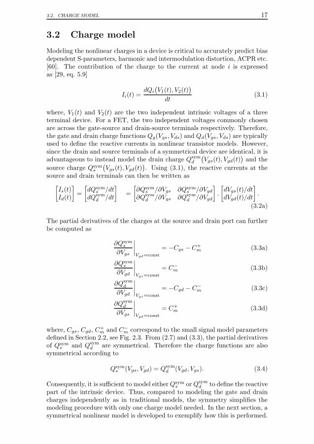
3 Nonlinear FET Model 15
3.1 Symmetrical models: An overview . . . . . . . . . . . . . . . . 163.2 Charge model . . . . . . . . . . . . . . . . . . . . . . . . . . . . 173.3 Symmetrical nonlinear model example . . . . . . . . . . . . . . 18
3.3.1 Nonlinear Current Model . . . . . . . . . . . . . . . . . 183.3.2 Nonlinear Charge Model . . . . . . . . . . . . . . . . . . 18
3.4 Model Validation . . . . . . . . . . . . . . . . . . . . . . . . . . 193.4.1 Small signal verification . . . . . . . . . . . . . . . . . . 203.4.2 Large-Signal Verification . . . . . . . . . . . . . . . . . . 21
4 Conclusions 23
4.1 Future work . . . . . . . . . . . . . . . . . . . . . . . . . . . . . 23
Acknowledgments 25
Bibliography 27
ix

x CONTENTS

Chapter 1
Introduction
The history of wireless communication starts with the work of Michael Fara-day, James Clerk Maxwell, Oliver Lodge, Heinrich Hertz, Jagadish ChandraBose, the 1909 Nobel Prize winner physicists Guglielmo Marconi and KarlFerdinand Braun. Michael Faraday’s work with the electric current carryingconductor and its local magnetic field inspired Maxwell who mathematicallypredicted the existence of electromagnetic waves of diverse wavelengths in1865 [1]. Later, Oliver Lodge and Heinrich Hertz confirmed the existence ofelectromagnetic waves in free space. Lodge’s work caught the attention of sci-entists in different countries including J. C. Bose in India who in 1894 gave thefirst public demonstration of wireless transmission using electromagnetic wavesto ring a bell and to explode a small charge of gunpowder from a distance [2].The wavelengths Bose used for his microwave experiments ranged from 2.5 cmto 5 mm (12 GHz to 60 GHz) [3]. Apart from Bose, the results from Hertzalso inspired Marconi, who made his first successful radio transmission exper-iments in 1895. He managed to send the information over a distance of 3 km.By 1901, the first transatlantic transmission was carried out between Poldhuin Cornwall and St. John’s in Newfoundland at a distance of 3200 km. Itwas Bose’s diode detector which received Marconi’s first transatlantic wirelesssignal [3], where the frequency of the wave used for the demonstration was 167kHz [4].
Today, the microwave frequency bands are densely populated with vari-ous applications like RADAR, satellite cellular telephone, GSM mobile, GPS,third and fourth generation cellular services, Bluetooth, etc. There are hardrequirements on applications for spectrum utilization and also a constant pushto move up in frequency for higher data rates. To reach high spectral efficiency,complex modulation schemes are used, which in turn require low distortion.Therefore, thorough understanding of the signal distorting mechanisms is re-quired. In such applications, transistors are one of the key components ofamplifiers, mixers, oscillators, switches, etc., and a major source of signal dis-tortion. With the demands for higher performance, rapid prototyping, as wellas lower cost for such systems and circuits, computer aided design (CAD)and simulation tools together with models for circuit elements have becomeincreasingly important. To predict intermodulation, output power, efficiency,etc., with high accuracy, a good nonlinear model for the transistor is required.
1

2 CHAPTER 1. INTRODUCTION
+
_
Vdse+
_Vgse
RF Swing
IN OUT
FET
Figure 1.1: A FET operating as shunt element in switch circuit where the drain-sourcevoltage becomes negative over a cycle of RF swing.
There are various nonlinear models available for different field-effect tran-sistor (FET) technologies. More than often, these transistors operate as anamplifier. Hence more focus is given to model the transistors in such operat-ing conditions. However, every model has its constraints. Unlike in amplifiers,FETs used in switch circuits have a different operating region. While thedrain-source voltage in amplifiers never goes negative (except for a highly mis-matched case), transistors used as shunt elements in switches also operatein the negative drain-source voltage region (see Fig. 1.1). Hence transistormodels suited for amplifiers do not necessarily predict the correct behaviorwhen operated as switch elements. There are some models available for switchFETs. Such transistors are often symmetrical around the gate (see Fig. 1.2a),a property which can drastically reduce the modeling complexity and is ad-dressed in the thesis. The modeling procedure discussed in this thesis is notrestricted to transistors used in switch circuits but is generic. Therefore theprocedure can be applied for any symmetrical device e.g., MOSFET, GaAspHEMTs/mHEMTs, InP HEMTs, etc., except power FETs (see Fig. 1.2b)where field-plates disturb the symmetry of the device [5–11].
Semi-insulating Substrate
Gate
HEMT Epilayers
S DLine of
Symmetry
(a)
Semi-insulating Substrate
Gate+FP1
FP2
HEMT Epilayers
S D
(b)
Figure 1.2: Cross-section of FETs used for switches and amplifiers: (a) symmetrical FET,(b) unsymmetrical power GaN FET with field plates [12, Fig. 1].
In this thesis, a new nonlinear modeling procedure is developed for sym-metrical FETs. The discussion starts with the traditional small signal model.From that, a new symmetrical small signal model is created in Chapter 2. Thismodel reflects the symmetry of the device forming a basis for a simplificationof the nonlinear modeling procedure [Paper A]. Further in the chapter, amodified optimization based extraction is used as a tool to improve the smallsignal extraction result for a symmetrical FET [Paper B]. In Chapter 3, anew nonlinear modeling technique is described where it is shown that only onecharge function is required to model the reactive part of the device [Paper A].Finally, the modeling procedure only dependent on the symmetry can be ex-tended to various other FET technologies and used to model transistors fordifferent applications, and thus setting up the path for the future work.

Chapter 2
Small Signal FET Model
Transistors are used extensively in microwave circuits and are excited withvarying terminal voltages. If the excitations are small enough, the nonlinearoperation of the device can be linearized at the operating point. Such an op-eration can be modeled by an equivalent circuit called small signal model. Itconsists of linear elements like resistors, transconductors, capacitors, etc., torepresent the small signal currents and charges in the device. These elementvalues are directly obtained from the partial derivatives of the currents andterminal charges. Small-signal models are good approximation for the transis-tors in many applications like small-signal amplifiers, oscillators etc. Moreover,they also serve as a basis for empirical nonlinear models, as will be describedin Chapter 3.
In this chapter, a new perspective on small-signal modeling is discussedbased on existing research and a new equivalent circuit is proposed for sym-metrical FETs. The first section of this chapter gives an overview on thetraditional small signal model and the development of a symmetrical equiv-alent circuit. Furthermore, the direct extraction method for the two modelsand its results are briefly described in Section 2.3. Finally in Section 2.4, amodified optimization based extraction is discussed which considers the sym-metry present in the device during extraction of small signal intrinsic modelparameters.
2.1 Traditional small signal model
The traditional small-signal model for FETs shown in Fig. 2.1 can be dividedinto two parts, extrinsic and intrinsic [13]. The extrinsic parameters (para-sitics) are bias independent elements which represent the connections to accessthe intrinsic device. The intrinsic parameters are commonly bias dependentand represent the physical operation of the active device. The 16-parametermodel shown in Fig. 2.1 is valid up to very high frequencies [13], and the modelalong with its variations has been widely used in previous modeling and cir-cuit design work [13–25]. Each of these models has the same intrinsic core.First, all of them have the two control voltages taken across the gate-sourceand drain-source nodes. Second, they contain one voltage controlled currentsource (VCCS) with the dependent voltage across the gate-source capacitance
3

4 CHAPTER 2. SMALL SIGNAL FET MODEL
ids = gm · Vgs and one conductance gds. The parameters gm and gds arecomputed from the derivatives of the resistive drain to source current Ids as
gm =∂Ids∂Vgs
∣∣∣∣Vds=const
(2.1a)
gds =∂Ids∂Vds
∣∣∣∣Vgs=const
. (2.1b)
Cgd
_
+
Vgs gm CmCds
gds
ids=gmVgs
ic =jωCmVgs
_
+
Vds
Ri
Rj
Gext
Lg
(Cpg)/2
Rg
Cgs
Dext
LdRd
(Cpd)/2
LsRs
(Cpg)/2 (Cpd)/2
Figure 2.1: The traditional small signal model of a common source field-effect transistorcontaining 16 parameters. The intrinsic part is shown inside the red rectangle.
The model shown in Fig. 2.1 is valid for both symmetrical and unsymmet-rical devices (see Fig. 1.2). However, due to the symmetry present in FETs(see Fig. 1.2a), the intrinsic source and drain ports are interchangeable. There-fore, a new equivalent circuit is developed in the next section where the devicesymmetry around the gate is exploited.
2.2 Symmetrical small signal model
Vgd
(V)
Vgs
(V
)
(mA)
−4 −3 −2 −1−4
−3
−2
−1
0
−20
−10
0
10
20
constV
gs(g
m− , g
ds)
constV
ds
constV
gd(g
m+ )
(gm
)
Figure 2.2: Contour plot of drain to source current of a symmetrical FET illustrating thedirection of current derivatives for parameters gm, gds, g
+m and g−m.
For a symmetrical device, the measured drain-source DC current showsthe symmetry in (Vgs,Vgd) bias grid, see Fig. 2.2. Therefore, (Vgs,Vgd) is a

2.2. SYMMETRICAL SMALL SIGNAL MODEL 5
better set of control voltages than (Vgs,Vds) to understand the symmetry inthe small signal model parameters [Paper A]. In the new control voltage set,whenever Vgs and Vgd are interchanged, the intrinsic parameters like (Cgs,Cgd)and (Ri,Rj) are interchanged thus existing in pairs. However, the VCCS in thetraditional model has the control voltage across Cgs, see Fig. 2.1. When thedrain and source terminals are interchanged, the control voltage for the VCCSmust also be taken across Cgd and not across Cgs. Therefore, the currentsource gm (see Fig. 2.1) is divided in to two independent VCCS controlled byVgs and Vgd respectively. The two new current sources are i+ds = g+m · Vgs andi−ds = g−m · Vgd where, g+m and g−m correspond to the derivatives of the resistivedrain to source current (see Fig. 2.2) as
g+m =∂Ids∂Vgs
∣∣∣∣Vgd=const
(2.2a)
g−m =−∂Ids∂Vgd
∣∣∣∣Vgs=const
. (2.2b)
Thus in the positive Vds region, g+m dominates over g−m and vice-versa. Notethat gm of the traditional model and g+m of the modified model are different.While gm is a derivative in constant Vds direction, g
+m is a derivative in constant
Vgd direction as seen in Fig. 2.2. Thus, g+m and g−m line up with the symmetryof the device observed in the (Vgs,Vgd) bias grid. Moreover, since the FET isa three terminal device, the two current-sources i+ds and i−ds are sufficient tomodel the small-signal resistive current, thereby making gds redundant. Theresulting equivalent circuit is shown in Fig. 2.3.
Cgd
SourceCgs
_+ Vgs
Gategm+ Cm
+ Cm
_gm
_
ids=gmVgs++
ic =jωCmVgs++
_+ Vgd
ids=gmVgd
_ _
__ic =jωCmVgd
Drain
Ri
Rj
Figure 2.3: Proposed symmetrical small signal intrinsic model with two anti-parallel currentsources and two transcapacitances.
While it is easy to measure current, we cannot measure charge. Therefore,we cannot plot the terminal charges in the (Vgs,Vgd) bias grid to illustrate thederivation of the transcapacitance in Fig. 2.3. However, the same reasoningis applied to the transcapacitance Cm in the traditional small signal model.Hence, Cm and Cds are replaced by C+
m and C−
m to build the symmetricalsmall signal model shown in Fig. 2.3. Similar to g+m and g−m, C+
m and C−
m arederivatives of the drain and source charges in constant Vgd and Vgs directionsrespectively. Thus in the new model, all the intrinsic parameters exist inpairs and their derivatives align to the set of control voltages (Vgs–Vgd). Theparameter extraction method for both the traditional and symmetrical modelsis briefly described in the next section.
6 CHAPTER 2. SMALL SIGNAL FET MODEL
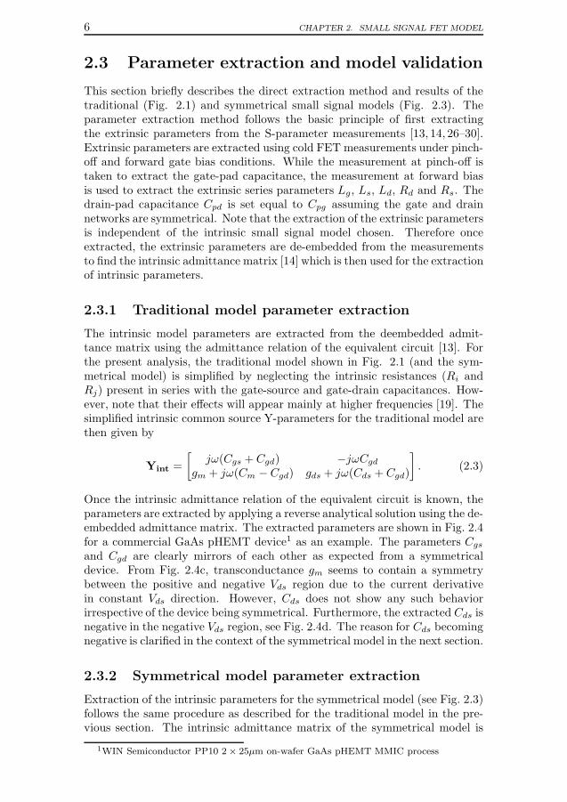
2.3 Parameter extraction and model validation
This section briefly describes the direct extraction method and results of thetraditional (Fig. 2.1) and symmetrical small signal models (Fig. 2.3). Theparameter extraction method follows the basic principle of first extractingthe extrinsic parameters from the S-parameter measurements [13, 14, 26–30].Extrinsic parameters are extracted using cold FET measurements under pinch-off and forward gate bias conditions. While the measurement at pinch-off istaken to extract the gate-pad capacitance, the measurement at forward biasis used to extract the extrinsic series parameters Lg, Ls, Ld, Rd and Rs. Thedrain-pad capacitance Cpd is set equal to Cpg assuming the gate and drainnetworks are symmetrical. Note that the extraction of the extrinsic parametersis independent of the intrinsic small signal model chosen. Therefore onceextracted, the extrinsic parameters are de-embedded from the measurementsto find the intrinsic admittance matrix [14] which is then used for the extractionof intrinsic parameters.
2.3.1 Traditional model parameter extraction
The intrinsic model parameters are extracted from the deembedded admit-tance matrix using the admittance relation of the equivalent circuit [13]. Forthe present analysis, the traditional model shown in Fig. 2.1 (and the sym-metrical model) is simplified by neglecting the intrinsic resistances (Ri andRj) present in series with the gate-source and gate-drain capacitances. How-ever, note that their effects will appear mainly at higher frequencies [19]. Thesimplified intrinsic common source Y-parameters for the traditional model arethen given by
Yint =
[jω(Cgs + Cgd) −jωCgd
gm + jω(Cm − Cgd) gds + jω(Cds + Cgd)
]
. (2.3)
Once the intrinsic admittance relation of the equivalent circuit is known, theparameters are extracted by applying a reverse analytical solution using the de-embedded admittance matrix. The extracted parameters are shown in Fig. 2.4for a commercial GaAs pHEMT device1 as an example. The parameters Cgs
and Cgd are clearly mirrors of each other as expected from a symmetricaldevice. From Fig. 2.4c, transconductance gm seems to contain a symmetrybetween the positive and negative Vds region due to the current derivativein constant Vds direction. However, Cds does not show any such behaviorirrespective of the device being symmetrical. Furthermore, the extracted Cds isnegative in the negative Vds region, see Fig. 2.4d. The reason for Cds becomingnegative is clarified in the context of the symmetrical model in the next section.
2.3.2 Symmetrical model parameter extraction
Extraction of the intrinsic parameters for the symmetrical model (see Fig. 2.3)follows the same procedure as described for the traditional model in the pre-vious section. The intrinsic admittance matrix of the symmetrical model is
1WIN Semiconductor PP10 2× 25µm on-wafer GaAs pHEMT MMIC process

2.3. PARAMETER EXTRACTION AND MODEL VALIDATION 7
Vgd
(V)
Vgs
(V
)
(fF)
AB
Vds
> 0 V
Vds
< 0 V
−4 −3 −2 −1 0−4
−3
−2
−1
0
10
20
30
40
50
60
70
(a) Cgs
Vgd
(V)
Vgs
(V
)
(fF)
A
B
−4 −3 −2 −1 0−4
−3
−2
−1
0
10
20
30
40
50
60
70
(b) Cgd
Vgd
(V)
Vgs
(V
)
(mS)
AB
−4 −3 −2 −1 0−4
−3
−2
−1
0
−50
0
50
(c) gm
Vgd
(V)
Vgs
(V
)
(fF)
AB
−4 −3 −2 −1 0−4
−3
−2
−1
0
−20
−10
0
10
20
30
(d) Cds
Figure 2.4: Bias dependence of the traditional small signal model intrinsic parameters ofthe DUT in an intrinsic Vgs−Vgd bias grid (a) Cgs (fF), (b) Cgd (fF), (c) gm (mS), (d) Cds
(fF).
given by
Ysymint =
[jω(Cgs + Cgd) −jωCgd
jω(C+m − Cgd − C−
m) + g+m − g−m jω(Cgd + C−
m) + g−m
]
(2.4)
where again the parameters Ri and Rj are neglected for simplification of theanalysis. The new parameters in (2.4) are related to the traditional modelparameters in (2.3) as
g−m = gds (2.5a)
g+m = gds + gm (2.5b)
C−
m = Cds (2.5c)
C+m = Cds + Cm. (2.5d)
Using (2.5), the proposed model parameters can also be directly calculatedfrom the traditional model parameters and are shown in Fig. 2.5.
For the symmetrical small signal model, the results clearly show that theparameters (g+m, g−m), (C+
m, C−
m) in Fig. 2.5 and (Cgs, Cgd) in Fig. 2.4 exist inpairs and are mirrors of one another along Vds = 0 V. This confirms the pro-posed symmetry for the device under test (DUT). Therefore, the parameters ofthe proposed model in the negative Vds region can be calculated by mirroringtheir corresponding parameters from the positive Vds bias region. The num-ber of measurement points can thus effectively be halved. Furthermore since

8 CHAPTER 2. SMALL SIGNAL FET MODEL
Vgd
(V)
Vgs
(V
)
(mS)
AB
Vds
> 0 V
Vds
< 0 V
−4 −3 −2 −1 0−4
−3
−2
−1
0
0
20
40
60
80
(a) g+m
Vgd
(V)
Vgs
(V
)
(mS)
AB
−4 −3 −2 −1 0−4
−3
−2
−1
0
0
20
40
60
80
(b) g−m
Vgd
(V)
Vgs
(V
)
(fF)
AB
−4 −3 −2 −1 0−4
−3
−2
−1
0
−10
0
10
20
30
(c) C+m
Vgd
(V)
Vgs
(V
)
(fF)
AB
−4 −3 −2 −1 0−4
−3
−2
−1
0
−20
−10
0
10
20
30
(d) C−
m
Figure 2.5: Bias dependence of the symmetrical small signal model intrinsic parameters ofthe DUT in an intrinsic Vgs − Vgd bias grid covering both the positive and negative Vds
region: (a) g+m (mS), (b) g−m (mS), (c) C+m (fF), and (d) C−
m (fF).
Cds and C−
m are equal as given by (2.5c), Cds in the negative Vds region (seeFig. 2.4d) is effectively a transcapacitor represented by C−
m in the symmetricalmodel (see Fig. 2.5d). This explains why Cds is negative in Fig. 2.4d.
2.3.3 Validation of model symmetry
For the validation of symmetry in the model shown in Fig. 2.3, the intrinsicmodel parameters in the negative Vds region are obtained by mirroring theextracted model in the positive Vds region. The model is validated by com-paring the mirrored model to the corresponding S-parameter measurements inthe negative Vds region. The difference between the measured and simulatedS-parameters using the mirrored model is computed using a mean square error(MSE) as
ǫ =2∑
j=1
2∑
k=1
1
max |Sjk|2
N∑
i=1
∣∣Sjk(ωi)− Smod
jk (ωi)∣∣2. (2.6)
The maximum modeling error given by (2.6) is obtained at bias point B wherethe model is mirrored from bias point A, marked in Fig. 2.4 and 2.5. For thevalidity of the symmetry in the model, S-parameters are compared at both biaspoint A and B and are shown in Fig. 2.6. The agreement between the simulated
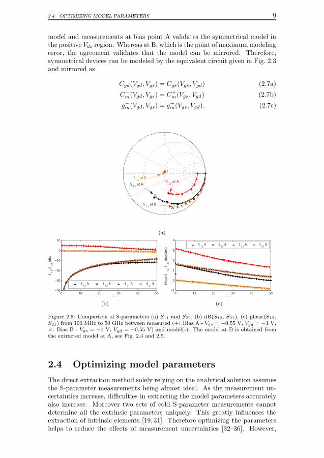
2.4. OPTIMIZING MODEL PARAMETERS 9
model and measurements at bias point A validates the symmetrical model inthe positive Vds region. Whereas at B, which is the point of maximummodelingerror, the agreement validates that the model can be mirrored. Therefore,symmetrical devices can be modeled by the equivalent circuit given in Fig. 2.3and mirrored as
Cgd(Vgd, Vgs) = Cgs(Vgs, Vgd) (2.7a)
C−
m(Vgd, Vgs) = C+m(Vgs, Vgd) (2.7b)
g−m(Vgd, Vgs) = g+m(Vgs, Vgd). (2.7c)
S22
at B
S11
at A
S11
at B
S22
at A
(a)
0 10 20 30 40 50−40
−30
−20
−10
0
10
Frequency (GHz)
S12, S
21 (dB)
S12 A S
12 B S
21 A S
21 B
(b)
0 10 20 30 40 50−1
0
1
2
3
4
Frequency (GHz)
Phase S
12, S
21 (Radians)
S12 A S
12 B S
21 A S
21 B
(c)
Figure 2.6: Comparison of S-parameters (a) S11 and S22, (b) dB(S12, S21), (c) phase(S12,S21) from 100 MHz to 50 GHz between measured (+: Bias A - Vgs = −0.55 V, Vgd = −1 V,×: Bias B - Vgs = −1 V, Vgd = −0.55 V) and model(-). The model at B is obtained fromthe extracted model at A, see Fig. 2.4 and 2.5.
2.4 Optimizing model parameters
The direct extraction method solely relying on the analytical solution assumesthe S-parameter measurements being almost ideal. As the measurement un-certainties increase, difficulties in extracting the model parameters accuratelyalso increase. Moreover two sets of cold S-parameter measurements cannotdetermine all the extrinsic parameters uniquely. This greatly influences theextraction of intrinsic elements [19, 31]. Therefore optimizing the parametershelps to reduce the effects of measurement uncertainties [32–36]. However,

10 CHAPTER 2. SMALL SIGNAL FET MODEL
the optimizer based extraction is computationally more intensive and it canconverge to a local minima. Therefore the sequential single parameter opti-mization proposed in [32, 33, 36] is used which is more robust against localminima. For better convergence, direct extraction results are used as seeds tothe optimizer [37–40]. The modeling error ǫ used for optimization is given by(2.6). To account for the symmetry, the optimizer is modified for extracting theintrinsic parameters and is verified for a commercial GaN device2 [Paper B].
2.4.1 Multibias extraction of parasitics
To extract the parasitics (or extrinsic parameters), the multibias extractionmethod from [36] is used. The method is based on the sequential single pa-rameter optimization [32, 33] at several bias points in different operating re-gions, see Fig. 2.7. Since the parasitics are bias independent, the methodsignificantly improves the estimation of the parasitics. Once the parasitics areextracted, the intrinsic parameters are extracted using a modified optimizerbased extraction described in the next section.
−15 −10 −5 0−15
−10
−5
0
Vds
> 0 V
Vds
< 0 V
Vgs
e (V
)
Vgde
(V)
Figure 2.7: Location of bias points (∗) for the multibias extraction in extrinsic Vgse - Vgde
bias grid.
2.4.2 Optimization of the symmetrical intrinsic parame-
ters
For the optimization based extraction, if the extrinsic resistance Rs and Rd
are similar [Paper B, Table I], intrinsic parameters can also be mirrored inthe extrinsic Vgse–Vgde bias grid. Therefore, the parameters can be optimizedin the extrinsic bias grid without the need of any interpolation algorithms.Furthermore, for the symmetrical model, the first important change in theoptimizer from [32, 33] is to optimize the intrinsic parameters for a bias pointtogether with the mirrored bias point in the other half using the same seedvalue, see Fig. 2.8. Moreover, the error function for such an optimizationprocess must have contributions from both the regions with equal weights.
While the main reason to use an optimizer is to reduce the modeling error,it is also important to obtain parameter values that are easier to fit into anonlinear model. Therefore, the direct extraction results are used as seeds
28× 100µm UMS GH25-10 V9C on-wafer GaN process

2.4. OPTIMIZING MODEL PARAMETERS 11
−15 −10 −5 0−15
−10
−5
0
Vds
> 0 V
Vds
< 0 V
1
2
3
4
5
6
2 3 4 5 6V
gse (
V)
Vgde
(V)
Figure 2.8: Arrows showing the direction of optimization with direct extraction results usedas seed shown by red (♦) in extrinsic Vgse - Vgde bias grid. The orange (♦) represent themirrored seeds for optimization in negative Vds region and number inside red and orange 2
represent sweep iterations.
at the first bias point and the optimized parameters are used as seed at thesubsequent bias points. This procedure is repeated for each sweep in the biasgrid to ensure smoothness, see Fig. 2.8. Note that the optimizer will facehigh gradient change in Cgs, g
+m and C+
m along the constant gate-drain voltageand in parameters Cgd, g
−
m and C−
m along the constant gate-source voltage.Therefore, the sweep direction (or direction of optimization) is chosen alongthe constant extrinsic drain-source voltage Vdse, see Fig. 2.8. The detailedsteps of optimization based extraction is described in section III in [Paper B].
2.4.3 Optimized parameters and model validation
Three of the six intrinsic parameters extracted using the modified sequentialoptimization method are shown in Fig. 2.9. The high gradient change is clearlyvisible along constant Vgde direction from the concentration of contour lines.The remaining intrinsic parameters (Cgd, C−
m, and g−m) are mirrored using(2.7).
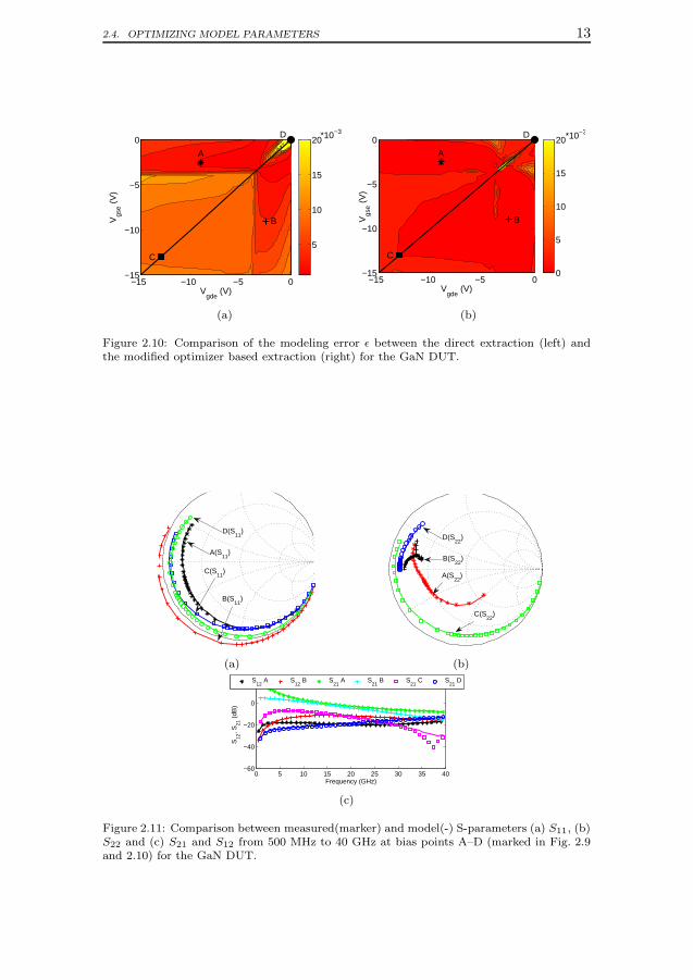
The benefit of the optimizer based extraction is to find a minima for thespecified error function and obtain results better than the direct extraction.Therefore, the modeling error given by (2.6) is compared for the direct andmodified optimizer based extraction in Fig. 2.10. While an improvement isobserved for the modified optimizer compared to the direct extraction re-sults, the optimizer based extraction shows higher error at Vgse = −3.25 V,Vgde = −3.25 V. This bias point is on the Vdse = 0 V line where the optimizerfails to model the steep gradient in all the intrinsic parameters near pinch-offof the transistor, see Fig. 2.9. This rise in error can be reduced by severalsimple techniques. First, a dense measurement grid around pinch-off will helpthe optimizer to model the change in parameter values in smaller step sizes.Second, to use the direct extraction results at the points where the optimizeris showing a rise in the error. And third, to use selective seeds, where the opti-mizer can choose whether to use the direct extraction result or the parametersfrom the previous or nearest optimized point as the seed value by comparingthe initial error. While the increase in error is limited to a very small region,the overall improvement in the modeling error verifies the applicability of the

12 CHAPTER 2. SMALL SIGNAL FET MODEL
Vgde
(V)
Vgs
e (V
)
(fF)
A
B
C
D
Vds
> 0 V
Vds
< 0 V
−15 −10 −5 0−15
−10
−5
0
200
300
400
500
600
700
(a) Cgs
Vgde
(V)
Vgs
e (V
) (fF)
A
B
C
D
−15 −10 −5 0−15
−10
−5
0
−100
0
100
200
300
(b) C+m
Vgde
(V)
Vgs
e (V
)
(mS)
A
B
C
D
−15 −10 −5 0−15
−10
−5
0
0
100
200
300
400
(c) g+m
Figure 2.9: Optimized small signal model intrinsic parameters in an extrinsic Vgse − Vgde
bias grid for a commercial GaN HEMT: (a) Cgs (fF), (b) C+m (fF), and (c) g+m (mS).
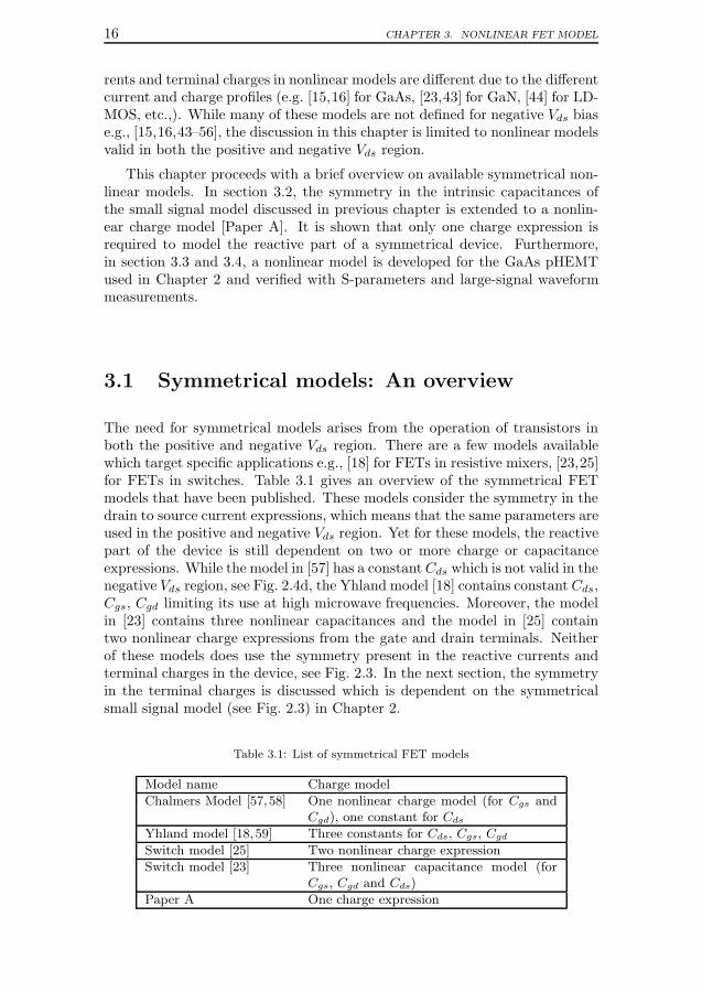
modified optimizer for extraction of the symmetrical model parameters. Toverify the optimized results, S-parameters are simulated at four bias pointsA–D (marked in Fig. 2.9 and 2.10) and compared to the measurements, seeFig. 2.11. A good match at all four bias points validate the modified optimizerbased extraction procedure.
2.4. OPTIMIZING MODEL PARAMETERS 13
Vgde
(V)
Vgs
e (V
)
*10−3
A
B
C
D
−15 −10 −5 0−15
−10
−5
0
5
10
15
20
(a)
Vgde
(V)
Vgs
e (V
)
*10−3
A
B
C
D
−15 −10 −5 0−15
−10
−5
0
0
5
10
15
20
(b)
Figure 2.10: Comparison of the modeling error ǫ between the direct extraction (left) andthe modified optimizer based extraction (right) for the GaN DUT.
D(S11
)
A(S11
)
C(S11
)
B(S11
)
(a)
D(S22
)
B(S22
)
A(S22
)
C(S22
)
(b)
0 5 10 15 20 25 30 35 40−60
−40
−20
0
20
Frequency (GHz)
S12
, S21
(dB
)
S12
A S12
B S21
A S21
B S21
C S21
D
(c)
Figure 2.11: Comparison between measured(marker) and model(-) S-parameters (a) S11, (b)S22 and (c) S21 and S12 from 500 MHz to 40 GHz at bias points A–D (marked in Fig. 2.9and 2.10) for the GaN DUT.

14 CHAPTER 2. SMALL SIGNAL FET MODEL

Chapter 3
Nonlinear FET Model
Microwave devices are often excited with large input signals causing themto operate nonlinearly. For that purpose, the small signal models discussedin Chapter 2 are not sufficient to predict the behavior of a transistor and anonlinear model is essential. There are three major approaches for modelingthe nonlinearities of a transistor. The first one is the physical model wherethe model is derived from the geometry and material data. This provides adirect link between the physical parameters and the electrical performance,and most models of silicon based transistors are derived this way [41]. Thesecond method is based on look-up tables where measured data provides acomplete experimental characterization of the electrical behavior e.g., [42].However, look-up table based models in general do not have the possibilityof extrapolation beyond the describing data set [29, pp. 130–135]. The thirdcategory is empirical models where the device model is created using linearand nonlinear lumped elements as shown in Fig. 3.1.
Cgd
Cgs
_+ Vgs
_+ Vgd
Ri
Rj
Gext
Lg
(Cpg)/2
Dext
LdRd
(Cpd)/2
Ls
Rs
Rg
Ids(Vgs,Vgd) C(Vgs,Vgd)
Figure 3.1: Nonlinear equivalent circuit for an FET showing linear and nonlinear elementsin common source configuration.
The empirical model shown in Fig. 3.1 is related to the small signal modelin Fig. 2.3 and is commonly used for microwave FETs. The linear and non-linear parameters in the nonlinear model are related to the small signal biasindependent and dependent parameters respectively. Since the small signalmodel is a linearization of the equivalent circuit in Fig. 3.1, the current andcharge (or capacitance) expressions can be obtained from the extracted smallsignal parameters [29, pp. 139–152]. The analytical expressions for the cur-
15
16 CHAPTER 3. NONLINEAR FET MODEL
rents and terminal charges in nonlinear models are different due to the differentcurrent and charge profiles (e.g. [15,16] for GaAs, [23,43] for GaN, [44] for LD-MOS, etc.,). While many of these models are not defined for negative Vds biase.g., [15,16,43–56], the discussion in this chapter is limited to nonlinear modelsvalid in both the positive and negative Vds region.
This chapter proceeds with a brief overview on available symmetrical non-linear models. In section 3.2, the symmetry in the intrinsic capacitances ofthe small signal model discussed in previous chapter is extended to a nonlin-ear charge model [Paper A]. It is shown that only one charge expression isrequired to model the reactive part of a symmetrical device. Furthermore,in section 3.3 and 3.4, a nonlinear model is developed for the GaAs pHEMTused in Chapter 2 and verified with S-parameters and large-signal waveformmeasurements.
3.1 Symmetrical models: An overview
The need for symmetrical models arises from the operation of transistors inboth the positive and negative Vds region. There are a few models availablewhich target specific applications e.g., [18] for FETs in resistive mixers, [23,25]for FETs in switches. Table 3.1 gives an overview of the symmetrical FETmodels that have been published. These models consider the symmetry in thedrain to source current expressions, which means that the same parameters areused in the positive and negative Vds region. Yet for these models, the reactivepart of the device is still dependent on two or more charge or capacitanceexpressions. While the model in [57] has a constant Cds which is not valid in thenegative Vds region, see Fig. 2.4d, the Yhland model [18] contains constant Cds,Cgs, Cgd limiting its use at high microwave frequencies. Moreover, the modelin [23] contains three nonlinear capacitances and the model in [25] containtwo nonlinear charge expressions from the gate and drain terminals. Neitherof these models does use the symmetry present in the reactive currents andterminal charges in the device, see Fig. 2.3. In the next section, the symmetryin the terminal charges is discussed which is dependent on the symmetricalsmall signal model (see Fig. 2.3) in Chapter 2.
Table 3.1: List of symmetrical FET models
Model name Charge model
Chalmers Model [57,58] One nonlinear charge model (for Cgs andCgd), one constant for Cds
Yhland model [18,59] Three constants for Cds, Cgs, Cgd
Switch model [25] Two nonlinear charge expression
Switch model [23] Three nonlinear capacitance model (forCgs, Cgd and Cds)
Paper A One charge expression
3.2. CHARGE MODEL 17
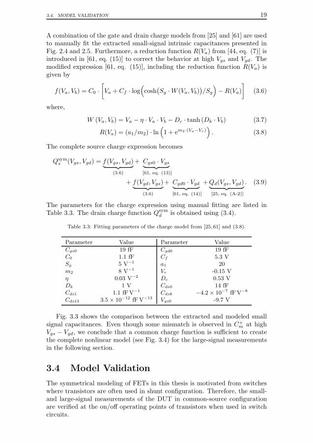
3.2 Charge model
Modeling the nonlinear charges in a device is critical to accurately predict biasdependent S-parameters, harmonic and intermodulation distortion, ACPR etc.[60]. The contribution of the charge to the current at node i is expressedas [29, eq. 5.9]
Ii(t) =dQi
(V1(t), V2(t)
)
dt(3.1)
where, V1(t) and V2(t) are the two independent intrinsic voltages of a threeterminal device. For a FET, the two independent voltages commonly chosenare across the gate-source and drain-source terminals respectively. Therefore,the gate and drain charge functions Qg(Vgs, Vds) and Qd(Vgs, Vds) are typicallyused to define the reactive currents in nonlinear transistor models. However,since the drain and source terminals of a symmetrical device are identical, it isadvantageous to instead model the drain charge Qsym
d
(Vgs(t), Vgd(t)
)and the
source charge Qsyms
(Vgs(t), Vgd(t)
). Using (3.1), the reactive currents at the
source and drain terminals can then be written as
[Is(t)Id(t)
]
=
[dQsym
s /dtdQsym
d /dt
]
=
[∂Qsym
s /∂Vgs ∂Qsyms /∂Vgd
∂Qsymd /∂Vgs ∂Qsym
d /∂Vgd
]
.
[dVgs(t)/dtdVgd(t)/dt
]
.
(3.2a)
The partial derivatives of the charges at the source and drain port can furtherbe computed as
∂Qsyms
∂Vgs
∣∣∣∣Vgd=const
= −Cgs − C+m (3.3a)
∂Qsyms
∂Vgd
∣∣∣∣Vgs=const
= C−
m (3.3b)
∂Qsymd
∂Vgd
∣∣∣∣Vgs=const
= −Cgd − C−
m (3.3c)
∂Qsymd
∂Vgs
∣∣∣∣Vgd=const
= C+m (3.3d)
where, Cgs, Cgd, C+m and C−
m correspond to the small signal model parametersdefined in Section 2.2, see Fig. 2.3. From (2.7) and (3.3), the partial derivativesof Qsym
s and Qsymd are symmetrical. Therefore the charge functions are also
symmetrical according to
Qsyms (Vgs, Vgd) = Qsym
d (Vgd, Vgs). (3.4)
Consequently, it is sufficient to model eitherQsyms orQsym
d to define the reactivepart of the intrinsic device. Thus, compared to modeling the gate and draincharges independently as in traditional models, the symmetry simplifies themodeling procedure with only one charge model needed. In the next section, asymmetrical nonlinear model is developed to exemplify how this is performed.

18 CHAPTER 3. NONLINEAR FET MODEL
3.3 Symmetrical nonlinear model example
For the symmetrical nonlinear model, the extrinsic and intrinsic small signalparameters extracted for the commercial GaAs pHEMT device1 in Chapter 2are used. The current and charge model is briefly described in the followingsubsections, respectively.
3.3.1 Nonlinear Current Model
To model the extracted small signal parameters g+m and g−m of the GaAspHEMT, the drain to source current (Ids) model in [18] is used. The modelparameters are obtained by manual fitting of the measured and modeled DCdata and are listed in Table 3.2. The comparison of the modeled and mea-sured current is shown in Fig. 3.2a validating the accuracy of the currentmodel. Although the measured current is symmetrical in Vgs–Vgd bias grid(see Fig. 3.2b), the current characteristics is not symmetrical in Fig. 3.2a sinceit is along constant Vgs lines.
Table 3.2: Model parameters for current [18].
Parameter φ g a b c d
Value 3 ° 0.043 A 0.02 V−1 2.8 V−1 0.23 V 12 V−1
−4 −3 −2 −1 0 1 2 3 4−25
−20
−15
−10
−5
0
5
10
15
20
25
Vdse
(V)
I dse (
mA
)
Vgs= −4 VVgs= −3.25 VVgs= −2.5 VVgs= −1.75 VVgs= −1 VVgs=−0.375 VVgs= −0.25 VVgs=−0.125 VVgs= 0 V
(a)
Vgde
(V)
Vgs
e (V
)
−4 −3 −2 −1 0−4
−3.5
−3
−2.5
−2
−1.5
−1
−0.5
0
−20
−15
−10
−5
0
5
10
15
20
(mA)
(b)
Figure 3.2: Yhland symmetrical current model for the GaAs DUT showing (a) comparisonof measured(marker) versus modeled(-) I-V characteristics, (b) contour plot of Ids with theconstant Vgs sweeps in the left figure drawn in corresponding colors.
3.3.2 Nonlinear Charge Model
For a symmetrical device, since it is sufficient to model one charge expression asexplained in section 3.2, the source-charge Qsym
s is considered in this example.Due to charge conservation, Qsym
s is related to the traditional gate and draincharges, Qg and Qd, respectively, by
Qsyms (Vgs, Vgd) = −Qg(Vgs, Vgd)−Qd(Vgs, Vgd). (3.5)
1WIN Semiconductor PP10 2× 25µm on-wafer GaAs pHEMT MMIC process
3.4. MODEL VALIDATION 19
A combination of the gate and drain charge models from [25] and [61] are usedto manually fit the extracted small-signal intrinsic capacitances presented inFig. 2.4 and 2.5. Furthermore, a reduction function R(Va) from [44, eq. (7)] isintroduced in [61, eq. (15)] to correct the behavior at high Vgs and Vgd. Themodified expression [61, eq. (15)], including the reduction function R(Va) isgiven by
f(Va, Vb) = C0 ·
[
Va + Cf · log(
cosh(Sg ·W (Va, Vb)
)/Sg
)
−R(Va)
]
(3.6)
where,
W (Va, Vb) = Va − η · Va · Vb −Dc · tanh (Dk · Vb) (3.7)
R(Va) = (a1/m2) · ln(
1 + em2·(Va−Vr))
. (3.8)
The complete source charge expression becomes
Qsyms (Vgs, Vgd) = f(Vgs, Vgd)
︸ ︷︷ ︸
(3.6)
+ Cgs0 · Vgs︸ ︷︷ ︸
[61, eq. (13)]
+ f(Vgd, Vgs)︸ ︷︷ ︸
(3.6)
+ Cgd0 · Vgd︸ ︷︷ ︸
[61, eq. (14)]
+Qd(Vgs, Vgd)︸ ︷︷ ︸
[25, eq. (A-2)]
. (3.9)
The parameters for the charge expression using manual fitting are listed inTable 3.3. The drain charge function Qsym
d is obtained using (3.4).
Table 3.3: Fitting parameters of the charge model from [25, 61] and (3.8).
Parameter Value Parameter Value
Cgs0 19 fF Cgd0 19 fFC0 1.1 fF Cf 5.3 VSg 5 V−1 a1 20m2 8 V−1 Vr -0.15 Vη 0.03 V−2 Dc 0.53 VDk 1 V Cds0 14 fFCds1 1.1 fFV−1 Cds8 −4.2× 10⁻⁷ fFV−8
Cds13 3.5× 10⁻¹² fFV−13 Vgs0 -9.7 V
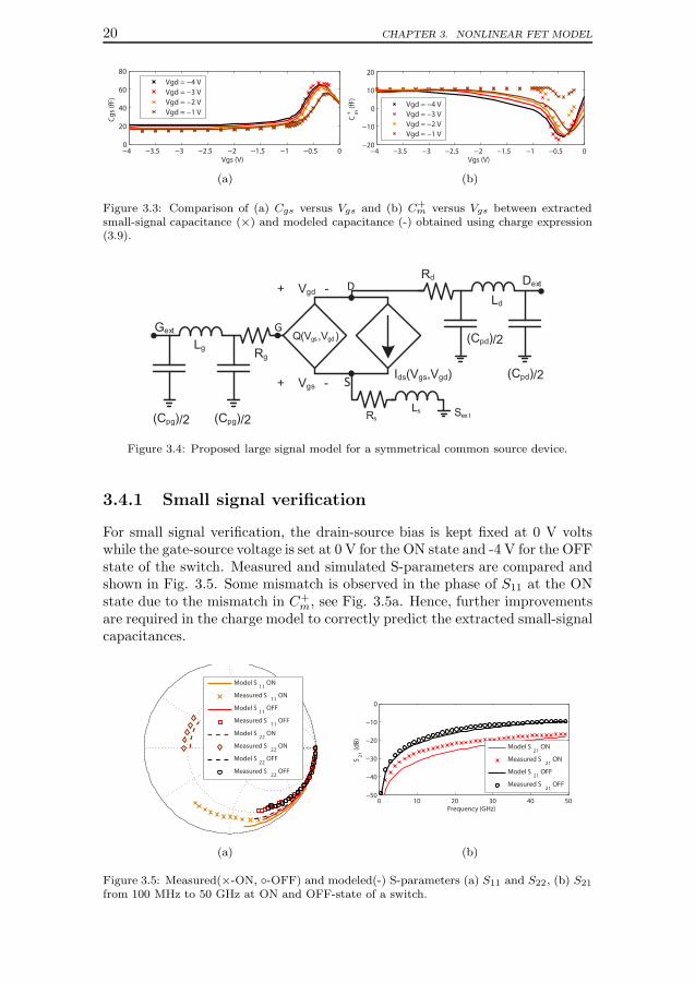
Fig. 3.3 shows the comparison between the extracted and modeled smallsignal capacitances. Even though some mismatch is observed in C+
m at highVgs − Vgd, we conclude that a common charge function is sufficient to createthe complete nonlinear model (see Fig. 3.4) for the large-signal measurementsin the following section.
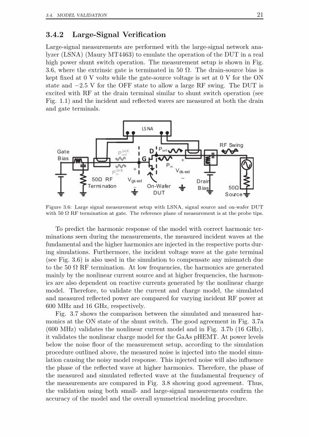
3.4 Model Validation
The symmetrical modeling of FETs in this thesis is motivated from switcheswhere transistors are often used in shunt configuration. Therefore, the small-and large-signal measurements of the DUT in common-source configurationare verified at the on/off operating points of transistors when used in switchcircuits.
20 CHAPTER 3. NONLINEAR FET MODEL
−4 −3.5 −3 −2.5 −2 −1.5 −1 −0.5 00
20
40
60
80
Vgs (V)
Cg
s (f
F)
Vgd = −4 V
Vgd = −3 V
Vgd = −2 V
Vgd = −1 V
(a)
−4 −3.5 −3 −2.5 −2 −1.5 −1 −0.5 0−20
−10
0
10
20
Vgs (V)
Cm+
(fF
)
Vgd = −4 V
Vgd = −3 V
Vgd = −2 V
Vgd = −1 V
(b)
Figure 3.3: Comparison of (a) Cgs versus Vgs and (b) C+m versus Vgs between extracted
small-signal capacitance (×) and modeled capacitance (-) obtained using charge expression(3.9).
Gext
Dext
Lg
(Cpg)/2
Rg
(Cpd)/2
Ld
Rd
Q(Vgs,Vgd)
Ids(Vgs,Vgd)
Sex tLs
Rs
G
S
D
+ Vgs -
+ Vgd -
(Cpd)/2
(Cpg)/2
Figure 3.4: Proposed large signal model for a symmetrical common source device.
3.4.1 Small signal verification
For small signal verification, the drain-source bias is kept fixed at 0 V voltswhile the gate-source voltage is set at 0 V for the ON state and -4 V for the OFFstate of the switch. Measured and simulated S-parameters are compared andshown in Fig. 3.5. Some mismatch is observed in the phase of S11 at the ONstate due to the mismatch in C+
m, see Fig. 3.5a. Hence, further improvementsare required in the charge model to correctly predict the extracted small-signalcapacitances.
Model S11
ON
Measured S11
ON
Model S11
OFF
Measured S11
OFF
Model S22
ON
Measured S22
ON
Model S22
OFF
Measured S22
OFF
(a)
0 10 20 30 40 50−50
−40
−30
−20
−10
0
Frequency (GHz)
S21 (dB)
Model S21 ON
Measured S21 ON
Model S21 OFF
Measured S21 OFF
(b)
Figure 3.5: Measured(×-ON, -OFF) and modeled(-) S-parameters (a) S11 and S22, (b) S21
from 100 MHz to 50 GHz at ON and OFF-state of a switch.
3.4. MODEL VALIDATION 21
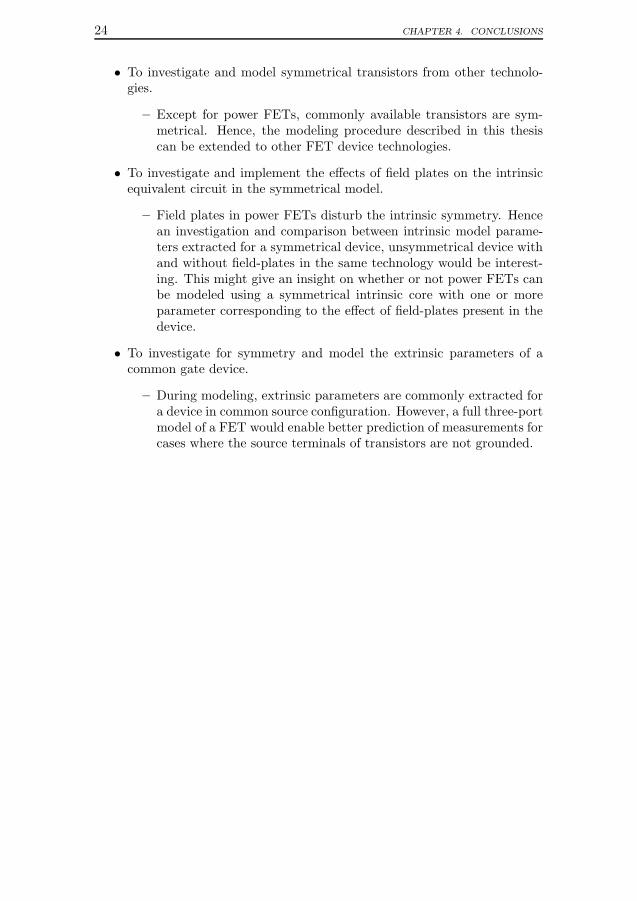
3.4.2 Large-Signal Verification
Large-signal measurements are performed with the large-signal network ana-lyzer (LSNA) (Maury MT4463) to emulate the operation of the DUT in a realhigh power shunt switch operation. The measurement setup is shown in Fig.3.6, where the extrinsic gate is terminated in 50 Ω. The drain-source bias iskept fixed at 0 V volts while the gate-source voltage is set at 0 V for the ONstate and −2.5 V for the OFF state to allow a large RF swing. The DUT isexcited with RF at the drain terminal similar to shunt switch operation (seeFig. 1.1) and the incident and reflected waves are measured at both the drainand gate terminals.
On-Wafer
DUT
G
D
50Ω RF
Termi nation
RF Swing
+
_Vgs ext
+
_Vds ext
Drain
B ias
Gate
B ias
LSNA
50Ω
Source
P in
PreflPrefl
GATE
PinGATE
Figure 3.6: Large signal measurement setup with LSNA, signal source and on-wafer DUTwith 50 Ω RF termination at gate. The reference plane of measurement is at the probe tips.
To predict the harmonic response of the model with correct harmonic ter-minations seen during the measurements, the measured incident waves at thefundamental and the higher harmonics are injected in the respective ports dur-ing simulations. Furthermore, the incident voltage wave at the gate terminal(see Fig. 3.6) is also used in the simulation to compensate any mismatch dueto the 50 Ω RF termination. At low frequencies, the harmonics are generatedmainly by the nonlinear current source and at higher frequencies, the harmon-ics are also dependent on reactive currents generated by the nonlinear chargemodel. Therefore, to validate the current and charge model, the simulatedand measured reflected power are compared for varying incident RF power at600 MHz and 16 GHz, respectively.
Fig. 3.7 shows the comparison between the simulated and measured har-monics at the ON state of the shunt switch. The good agreement in Fig. 3.7a(600 MHz) validates the nonlinear current model and in Fig. 3.7b (16 GHz),it validates the nonlinear charge model for the GaAs pHEMT. At power levelsbelow the noise floor of the measurement setup, according to the simulationprocedure outlined above, the measured noise is injected into the model simu-lation causing the noisy model response. This injected noise will also influencethe phase of the reflected wave at higher harmonics. Therefore, the phase ofthe measured and simulated reflected wave at the fundamental frequency ofthe measurements are compared in Fig. 3.8 showing good agreement. Thus,the validation using both small- and large-signal measurements confirm theaccuracy of the model and the overall symmetrical modeling procedure.

22 CHAPTER 3. NONLINEAR FET MODEL
−15 −10 −5 0 5 10−90
−80
−70
−60
−50
−40
−30
−20
−10
0
10
Pin
(dBm)
Pre
! (
dB
m)
(a)
−20 −15 −10 −5 0 5 10−90
−80
−70
−60
−50
−40
−30
−20
−10
0
Pin
(dBm)
Pre
! (
dB
m)
(b)
Figure 3.7: Comparison between magnitude of the measured (fundamental frequency: ×,second harmonic: and, third harmonic: +) and simulated(-) reflected versus incidentpower at the drain of the DUT at (a) 600 MHz, (b) 16 GHz at the ON state (Vgse = 0 V,Vdse = 0 V). For OFF-state validation, see Fig. 14 in [Paper A].
−20 −15 −10 −5 0 5 10264
266
268
270
272
274
Pin
(dBm)
Pha
se R
efle
cted
wav
e (D
eg)
(a)
−20 −15 −10 −5 0 5 1085
90
95
100
105
Pin
(dBm)
Pha
se R
efle
cted
wav
e (D
eg)
(b)
Figure 3.8: Comparison between the model (-) and measured (: 600 MHz, +: 16 GHz)phase of the reflected wave (Prefl) at the drain port for the fundamental frequencies (a) atOFF state (Vgse = −2.5 V, Vdse = 0 V, and (b) at ON state (Vgse = 0 V, Vdse = 0 V ofthe DUT.

Chapter 4
Conclusions
In this thesis, the emphasis is on the device symmetry as an important fea-ture to simplify the empirical modeling and parameters extraction methodsfor FETs. While the modeling procedure is based on existing techniques, thedevice symmetry leads to a new small-signal equivalent model. The proposedmodel allows mirroring of the parameters between the positive and negativedrain-source regions, thus reducing the number of measurements by half [Pa-per A]. The work is validated using a commercial GaAs FET. Further, thesymmetrical equivalent model parameters are optimized using a modified opti-mization based extraction to take the symmetry into consideration [Paper B].The optimization of parameters was performed on a commercial GaN HEMTshowing that the symmetrical equivalent circuit is also a generic FET smallsignal model. Furthermore, the symmetrical small-signal model was extendedto a nonlinear model, where a proper use of the device symmetry allowed thereactive parts of the intrinsic device to be modeled using a single commoncharge expression. Thus, effectively simplifying the nonlinear model and re-ducing the number of charge expressions to define the model [Paper A]. Eventhough the modeling work is motivated from transistors used in switch cir-cuits, the procedure is generic to all symmetrical FETs and can be extendedto other technologies.
4.1 Future work
During the work with this thesis, several interesting topics for future workhave emerged and are hereby listed:
• Better and robust extraction of the common charge function with re-duced number of parameters.
– Further work is required to improve the charge model developed forthe GaAs DUT based on existing expressions. A common chargeexpression also opens up the possibility of modeling the nonlinearreactive part of a symmetrical device with fewer parameters.
• To validate the model with an MMIC circuit design.
23
24 CHAPTER 4. CONCLUSIONS
• To investigate and model symmetrical transistors from other technolo-gies.
– Except for power FETs, commonly available transistors are sym-metrical. Hence, the modeling procedure described in this thesiscan be extended to other FET device technologies.
• To investigate and implement the effects of field plates on the intrinsicequivalent circuit in the symmetrical model.
– Field plates in power FETs disturb the intrinsic symmetry. Hencean investigation and comparison between intrinsic model parame-ters extracted for a symmetrical device, unsymmetrical device withand without field-plates in the same technology would be interest-ing. This might give an insight on whether or not power FETs canbe modeled using a symmetrical intrinsic core with one or moreparameter corresponding to the effect of field-plates present in thedevice.
• To investigate for symmetry and model the extrinsic parameters of acommon gate device.
– During modeling, extrinsic parameters are commonly extracted fora device in common source configuration. However, a full three-portmodel of a FET would enable better prediction of measurements forcases where the source terminals of transistors are not grounded.

Acknowledgment
I would like to express my gratitude to all the people that made this workpossible.
First, I would like to thank my examiner Prof. Herbert Zirath for giv-ing me the opportunity to work and conduct this research at the MicrowaveElectronics Laboratory. I would also to thank Prof. Jan Grahn for creating agreat working environment here in the GigaHertz Centre and to arrange fundsfor advance research projects done at Microwave Electronics Laboratory atChalmers.
My deepest gratitude to supervisor Assoc. Prof. Christian Fager, Asst.Prof. Mattias Thorsell and Adj. Prof. Klas Yhland for guidance, encourage-ment and support throughout the course of this work. A special mention ofChristian for being a great source of knowledge and ideas, Mattias for makingmeasurements and the setup look so simple yet so much insightful, and Klasfor broadening the context of the work and my horizons.
I would also like to thank Assoc. Prof. Iltcho Angelov, Assoc. Prof. HansHjelmgren and Assoc. Prof. Niklas Rorsman for sharing their knowledge onthe subject. Henric and Jan are acknowledged for IT-support.
I really appreciate the beautiful working environment at MC2 created bymy friends and colleagues.
My wife Sneha and my family have been the biggest strength and reasonfor me to keep moving on with this work.
This research has been carried out in the GigaHertz Centre in a jointproject financed by the Swedish Governmental Agency of Innovation Systems(VINNOVA), Chalmers University of Technology, SP Technical Research Insti-tute of Sweden, ComHeat Microwave AB, Ericsson AB, Infineon TechnologiesAG, Mitsubishi Electric Corporation, NXP Semiconductors BV, Saab AB andUnited Monolithic Semiconductors.
25

Bibliography
[1] D. Emerson, “The work of Jagadis Chandra Bose: 100 years of millimeter-wave research,” IEEE Trans. Microw. Theory Techn., vol. 45, no. 12, pp.2267–2273, Dec 1997.
[2] T. Sarkar and D. L. Sengupta, “An appreciation of J.C. Bose’s pioneeringwork in millimeter waves,” IEEE Antennas and Propagation Magazine,vol. 39, no. 5, pp. 55–62, Oct 1997.
[3] P. Bondyopadhyay, “Sir J.C. Bose diode detector received Marconi’s firsttransatlantic wireless signal of December 1901 (the “Italian Navy Co-herer” Scandal Revisited),” Proceedings of the IEEE, vol. 86, no. 1, pp.259–285, Jan 1998.
[4] ——, “Guglielmo Marconi - The father of long distance radio commu-nication - An engineer’s tribute,” in Microwave Conference, 1995. 25thEuropean, vol. 2, Sept 1995, pp. 879–885.
[5] N.-Q. Zhang, S. Keller, G. Parish, S. Heikman, S. DenBaars, andU. Mishra, “High breakdown GaN HEMT with overlapping gate struc-ture,” IEEE Electron Device Lett., vol. 21, no. 9, pp. 421–423, Sept 2000.
[6] S. Karmalkar and U. K. Mishra, “Enhancement of breakdown voltage inAlGaN/GaN high electron mobility transistors using a field plate,” IEEETrans. Electron. Devices, vol. 48, no. 8, pp. 1515–1521, Aug 2001.
[7] Y. Ando, Y. Okamoto, H. Miyamoto, T. Nakayama, T. Inoue, andM. Kuzuhara, “10-W/mm AlGaN-GaN HFET with a field modulatingplate,” IEEE Electron Device Lett., vol. 24, no. 5, pp. 289–291, May 2003.
[8] A. Wakejima, K. Ota, K. Matsunaga, and M. Kuzuhara, “A GaAs-basedfield-modulating plate HFET with improved WCDMA peak-output-power characteristics,” IEEE Trans. Electron. Devices, vol. 50, no. 9, pp.1983–1987, Sept 2003.
[9] Y. F. Wu, A. Saxler, M. Moore, R. Smith, S. Sheppard, P. Chavarkar,T. Wisleder, U. Mishra, and P. Parikh, “30-W/mm GaN HEMTs by fieldplate optimization,” IEEE Electron Device Lett., vol. 25, no. 3, pp. 117–119, March 2004.
[10] S. Karmalkar, M. Shur, G. Simin, and M. A. Khan, “Field-plate engi-neering for HFETs,” IEEE Trans. Electron. Devices, vol. 52, no. 12, pp.2534–2540, Dec 2005.
27

28 BIBLIOGRAPHY
[11] C.-Y. Chiang, H.-T. Hsu, and E. Y. Chang, “Effect of Field Plate onthe RF Performance of AlGaN/GaN HEMT Devices,” Physics Procedia,vol. 25, pp. 86 – 91, 2012, international Conference on Solid State Devicesand Materials Science, April 1-2, 2012, Macao.
[12] R. Pengelly, S. Wood, J. Milligan, S. Sheppard, and W. Pribble, “AReview of GaN on SiC High Electron-Mobility Power Transistors andMMICs,” IEEE Trans. Microw. Theory Techn., vol. 60, no. 6, pp. 1764–1783, June 2012.
[13] N. Rorsman, M. Garcia, C. Karlsson, and H. Zirath, “Accurate small-signal modeling of HFET’s for millimeter-wave applications,” IEEETrans. Microw. Theory Techn., vol. 44, no. 3, pp. 432–437, 1996.
[14] G. Dambrine, A. Cappy, F. Heliodore, and E. Playez, “A new methodfor determining the FET small-signal equivalent circuit,” IEEE Trans.Microw. Theory Tech., vol. 36, no. 7, pp. 1151–1159, Jul 1988.
[15] W. Curtice and M. Ettenberg, “A Nonlinear GaAs FET Model for Usein the Design of Output Circuits for Power Amplifiers,” IEEE Trans.Microw. Theory Tech., vol. 33, no. 12, pp. 1383–1394, 1985.
[16] I. Angelov, H. Zirath, and N. Rosman, “A new empirical nonlinear modelfor HEMT and MESFET devices,” IEEE Trans. Microw. Theory Tech.,vol. 40, no. 12, pp. 2258–2266, 1992.
[17] W. Curtice, J. Pla, D. Bridges, T. Liang, and E. Shumate, “A new dy-namic electro-thermal nonlinear model for silicon RF LDMOS FETs,” inIEEE MTT-S Int. Microw. Symp. Dig., vol. 2, June 1999, pp. 419–422.
[18] K. Yhland, N. Rorsman, M. Garcia, and H. Merkel, “A symmetricalnonlinear HFET/MESFET model suitable for intermodulation analysisof amplifiers and resistive mixers,” IEEE Trans. Microw. Theory Tech.,vol. 48, no. 1, pp. 15–22, 2000.
[19] C. Fager, L. Linner, and J. Pedro, “Optimal parameter extraction and un-certainty estimation in intrinsic FET small-signal models,” IEEE Trans.Microw. Theory Tech., vol. 50, no. 12, pp. 2797–2803, 2002.
[20] M. Wren and T. Brazil, “Enhanced prediction of pHEMT nonlinear dis-tortion using a novel charge conservative model,” in IEEE MTT-S Int.Microw. Symp. Dig., vol. 1, 2004, pp. 31–34.
[21] A. Jarndal and G. Kompa, “A new small-signal modeling approach ap-plied to GaN devices,” IEEE Trans. Microw. Theory Techn., vol. 53,no. 11, pp. 3440–3448, Nov 2005.
[22] W. Choi, G. Jung, J. Kim, and Y. Kwon, “Scalable Small-Signal Modelingof RF CMOS FET Based on 3-D EM-Based Extraction of Parasitic Effectsand Its Application to Millimeter-Wave Amplifier Design,” IEEE Trans.Microw. Theory Techn., vol. 57, no. 12, pp. 3345–3353, Dec 2009.

BIBLIOGRAPHY 29
[23] G. Callet, J. Faraj, O. Jardel, C. Charbonniaud, J.-C. Jacquet,T. Reveyrand, E. Morvan, S. Piotrowicz, J.-P. Teyssier, and R. Quere,“A new nonlinear HEMT model for AlGaN/GaN switch applications,”Int. J.Microw. Wireless Technol. (Special Issue), vol. 2, no. 3-4, pp. 283–291, Jul. 2010.
[24] B. S. Mahalakshmi, S. Manikantan, P. Bhavana, M. P. Anand, R. SaiEk-naath, and M. N. Devi, “Small signal modelling of GaN HEMT at70GHz,” in International Conference on Signal Processing and IntegratedNetworks (SPIN), Feb 2014, pp. 739–743.
[25] S. Takatani and C.-D. Chen, “Nonlinear Steady-State III-V FET Modelfor Microwave Antenna Switch Applications,” IEEE Trans. Electron. De-vices, vol. 58, no. 12, pp. 4301–4308, 2011.
[26] W. Curtice and R. Camisa, “Self-Consistent GaAs FETModels for Ampli-fier Design and Device Diagnostics,” IEEE Trans. Microw. Theory Techn.,vol. 32, no. 12, pp. 1573–1578, Dec 1984.
[27] R. Tayrani, J. E. Gerber, T. Daniel, R. S. Pengelly, and U. L. Rohde, “Anew and reliable direct parasitic extraction method for MESFETs andHEMTs,” in EuMIC, Sept 1993, pp. 451–453.
[28] T.-H. Chen and M. Kumar, “Novel GaAs FET modeling technique forMMICs,” in Gallium Arsenide Integrated Circuit (GaAs IC) Symposium,1988. Technical Digest 1988., 10th Annual IEEE, Nov 1988, pp. 49–52.
[29] M. Rudolph, C. Fager, and D. Root, Nonlinear Transistor Model Pa-rameter Extraction Techniques, ser. The Cambridge RF and MicrowaveEngineering Series. Cambridge University Press, 2011.
[30] E. Arnold, M. Golio, M. Miller, and B. Beckwith, “Direct extraction ofgaas mesfet intrinsic element and parasitic inductance values,” in IEEEMTT-S Int. Microw. Symp. Dig., May 1990, pp. 359–362 vol.1.
[31] F. King, P. Winson, A. Snider, L. Dunleavy, and D. Levinson, “Mathmethods in transistor modeling: Condition numbers for parameter extrac-tion,” IEEE Trans. Microw. Theory Techn., vol. 46, no. 9, pp. 1313–1314,Sep 1998.
[32] C. van Niekerk and P. Meyer, “A new approach for the extraction of an fetequivalent circuit from measured s parameters,” Microwave and OpticalTechnology Letters, vol. 11, no. 5, pp. 281–284, 1996.
[33] H. Kondoh, “An Accurate FET Modelling from Measured S-Parameters,”in IEEE MTT-S Int. Microw. Symp. Dig., June 1986, pp. 377–380.
[34] A. Patterson, V. Fusco, J. J. McKeown, and J. Stewart, “A systematicoptimization strategy for microwave device modelling,” IEEE Trans. Mi-crow. Theory Techn., vol. 41, no. 3, pp. 395–405, Mar 1993.
[35] C. van Niekerk and P. Meyer, “Performance and limitations ofdecomposition-based parameter extraction procedures for FET small-signal models,” IEEE Trans. Microw. Theory Techn., vol. 46, no. 11,pp. 1620–1627, Nov 1998.

30 BIBLIOGRAPHY
[36] C. van Niekerk, P. Meyer, D. M. M. P. Schreurs, and P. Winson, “Arobust integrated multibias parameter-extraction method for MESFETand HEMT models,” IEEE Trans. Microw. Theory Techn., vol. 48, no. 5,pp. 777–786, May 2000.
[37] K. Shirakawa, H. Oikawa, T. Shimura, Y. Kawasaki, Y. Ohashi, T. Saito,and Y. Daido, “An approach to determining an equivalent circuit forHEMTs,” IEEE Trans. Microw. Theory Techn., vol. 43, no. 3, pp. 499–503, Mar 1995.
[38] B.-L. Ooi, M.-S. Leong, and P.-S. Kooi, “A novel approach for determin-ing the GaAs MESFET small-signal equivalent-circuit elements,” IEEETrans. Microw. Theory Techn., vol. 45, no. 12, pp. 2084–2088, Dec 1997.
[39] F. Lin and G. Kompa, “FET model parameter extraction based on opti-mization with multiplane data-fitting and bidirectional search-a new con-cept,” IEEE Trans. Microw. Theory Techn., vol. 42, no. 7, pp. 1114–1121,Jul 1994.
[40] C. Campbell and S. Brown, “An analytic method to determine GaAs FETparasitic inductances and drain resistance under active bias conditions,”IEEE Trans. Microw. Theory Techn., vol. 49, no. 7, pp. 1241–1247, Jul2001.
[41] Y. Tsividis, Operation and Modeling of the MOS Transistor. OxfordUniversity Press, 1999.
[42] A. Rofougaran and A. Abidi, “A table lookup FET model for accurateanalog circuit simulation,” IEEE Trans. Comput.-Aided Design Integr.Circuits Syst., vol. 12, no. 2, pp. 324–335, Feb 1993.
[43] I. Angelov, K. Andersson, D. Schreurs, D. Xiao, N. Rorsman, V. Desmaris,M. Sudow, and H. Zirath, “Large-signal modelling and comparison ofAlGaN/GaN HEMTs and SiC MESFETs,” in APMC, Dec 2006, pp. 279–282.
[44] C. Fager, J. Pedro, N. de Carvalho, and H. Zirath, “Prediction of IMDin LDMOS transistor amplifiers using a new large-signal model,” IEEETrans. Microw. Theory Techn., vol. 50, no. 12, pp. 2834–2842, Dec 2002.
[45] A. McCamant, G. McCormack, and D. Smith, “An improved GaAs MES-FET model for SPICE,” IEEE Trans. Microw. Theory Techn., vol. 38,no. 6, pp. 822–824, Jun 1990.
[46] I. Angelov, L. Bengtsson, and M. Garcia, “Extensions of the Chalmersnonlinear HEMT and MESFET model,” IEEE Trans. Microw. TheoryTechn., vol. 44, no. 10, pp. 1664–1674, Oct 1996.
[47] L.-S. Liu, J.-G. Ma, and G.-I. Ng, “Electrothermal Large-Signal Model ofIII-V FETs Including Frequency Dispersion and Charge Conservation,”IEEE Trans. Microw. Theory Tech., vol. 57, no. 12, pp. 3106–3117, 2009.
BIBLIOGRAPHY 31
[48] K. Yuk and G. Branner, “An Empirical Large-Signal Model for SiC MES-FETs With Self-Heating Thermal Model,” IEEE Trans. Microw. TheoryTechn., vol. 56, no. 11, pp. 2671–2680, Nov 2008.
[49] W. Curtice, “A MESFET Model for Use in the Design of GaAs IntegratedCircuits,” IEEE Trans. Microw. Theory Techn., vol. 28, no. 5, pp. 448–456, May 1980.
[50] J. Pedro, “A physics-based MESFET empirical model,” in IEEE MTT-SInt. Microw. Symp. Dig., May 1994, pp. 973–976 vol.2.
[51] D. Halchin, M. Miller, M. Golio, and S. Tehrani, “HEMT models for largesignal circuit simulation,” in IEEE MTT-S Int. Microw. Symp. Dig., May1994, pp. 985–988 vol.2.
[52] Agilent Technologies, “TriQuint Scalable Nonlin-ear GaAsFET Model.” [Online]. Available: http://cp.literature.agilent.com/litweb/pdf/ads2008/ccnld/ads2008/TOM Model (TriQuint Scalable Nonlinear GaAsFET Model).html
[53] ——, “TriQuint TOM3 Scalable Nonlinear FET Model.” [On-line]. Available: http://cp.literature.agilent.com/litweb/pdf/ads2008/ccnld/ads2008/TOM3 Model (TriQuint TOM3 Scalable NonlinearFET Model).html
[54] ——, “Tajima GaAsFET Model.” [Online]. Avail-able: http://cp.literature.agilent.com/litweb/pdf/ads2008/ccnld/ads2008/Tajima Model (Tajima GaAsFET Model).html
[55] ——, “Materka GaAsFET Model.” [Online]. Avail-able: http://cp.literature.agilent.com/litweb/pdf/ads2008/ccnld/ads2008/Materka Model (Materka GaAsFET Model).html
[56] H. Statz, P. Newman, I. Smith, R. A. Pucel, and H. Haus, “GaAs FETdevice and circuit simulation in SPICE,” IEEE Trans. Electron. Devices,vol. 34, no. 2, pp. 160–169, Feb 1987.
[57] I. Angelov, V. Desmaris, K. Dynefors, P. A. Nilsson, N. Rorsman, andH. Zirath, “On the large-signal modelling of AlGaN/GaN HEMTs andSiC MESFETs,” in Proceeding of the 13th Gass Symposium Paris, Oct2005, pp. 309–312.
[58] Agilent Technologies, “Angelov Nonlinear GaAsFET Model.”[Online]. Available: http://cp.literature.agilent.com/litweb/pdf/ads2008/ccnld/ads2008/Angelov Model (Angelov (Chalmers)Nonlinear GaAsFET Model).html
[59] AWR Corporation, “Yhland MESFET Model.” [Online]. Available:https://awrcorp.com/download/faq/english/docs/Elements/yhland.htm
[60] D. Root, “Nonlinear charge modeling for FET large-signal simulation andits importance for IP3 and ACPR in communication circuits,” in IEEEMidwest Circuits Syst. Symp., vol. 2, 2001, pp. 768–772 vol.2.

32 BIBLIOGRAPHY
[61] C.-J. Wei, Y. Tkachenko, and D. Bartle, “An accurate large-signal modelof GaAs MESFET which accounts for charge conservation, dispersion,and self-heating,” IEEE Trans. Microw. Theory Techn., vol. 46, no. 11,pp. 1638–1644, 1998.