symmetry demanded topological nodal-line materials - arxiv · symmetry demanded topological...
TRANSCRIPT
Symmetry Demanded Topological Nodal-line Materials
Shuo-Ying Yang,1 Hao Yang,1, 2 Elena Derunova,1 Stuart S. P. Parkin,1 Binghai Yan,2, 3 and Mazhar N. Ali1, ∗
1Max Planck Institute of Microstructure Physics, Weinberg 2, 06120 Halle, Germany2Max Planck Institute for Chemical Physics of Solids, 01187 Dresden, Germany
3Department of Condensed Matter Physics, Weizmann Institute of Science, Rehovot 76100, Israel
The realization of Dirac and Weyl physics in solids has made topological materials one of the main focusesof condensed matter physics. Recently, the topic of topological nodal line semimetals, materials in which Diracor Weyl-like crossings along special lines in momentum space create either a closed ring or line of degenera-cies, rather than discrete points, has become a hot topic in topological quantum matter. Here we review theexperimentally confirmed and theoretically predicted topological nodal line semimetals, focusing in particularon the symmetry protection mechanisms of the nodal lines in various materials. Three different mechanisms: acombination of inversion and time-reversal symmetry, mirror reflection symmetry, and non-symmorphic sym-metry, and their robustness under the effect of spin orbit coupling are discussed. We also present a new Weylnodal line material, the Te-square net compound KCu2EuTe4, which has several Weyl nodal lines including oneextremely close to the Fermi level (<30 meV below EF). Finally, we discuss potential experimental signaturesfor observing exotic properties of nodal line physics.
I. INTRODUCTION
Topologically nontrivial states of matter have been of greatinterest in the field of topological quantum materials duringthe past decade for their rich and novel physics. The fieldwas ignited after the discovery of topological insulators (TIs)- materials that exhibit robust metallic surface states protectedby the topology in the insulating bulk1,2. Recently, topologicalsemimetals (TSM) such as Dirac and Weyl semimetals werediscovered which can also host metallic surface states with asemi-metallic bulk3.
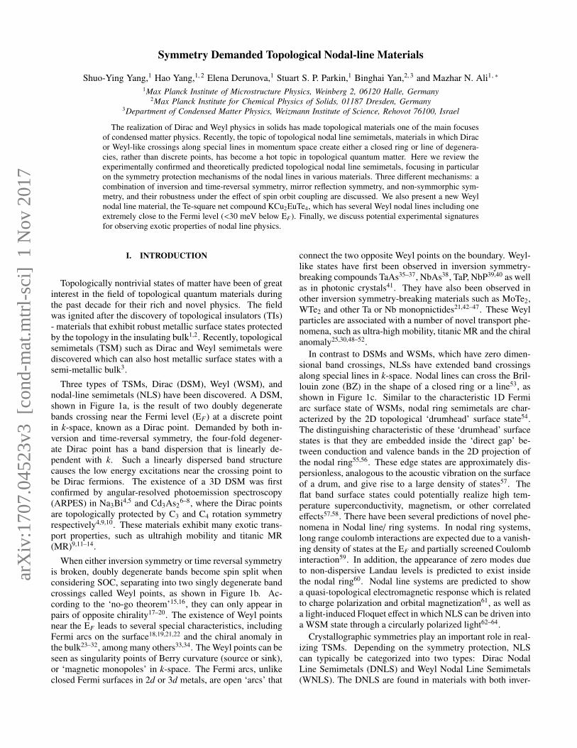
Three types of TSMs, Dirac (DSM), Weyl (WSM), andnodal-line semimetals (NLS) have been discovered. A DSM,shown in Figure 1a, is the result of two doubly degeneratebands crossing near the Fermi level (EF) at a discrete pointin k-space, known as a Dirac point. Demanded by both in-version and time-reversal symmetry, the four-fold degener-ate Dirac point has a band dispersion that is linearly de-pendent with k. Such a linearly dispersed band structurecauses the low energy excitations near the crossing point tobe Dirac fermions. The existence of a 3D DSM was firstconfirmed by angular-resolved photoemission spectroscopy(ARPES) in Na3Bi4,5 and Cd3As2
6–8, where the Dirac pointsare topologically protected by C3 and C4 rotation symmetryrespectively4,9,10. These materials exhibit many exotic trans-port properties, such as ultrahigh mobility and titanic MR(MR)9,11–14.
When either inversion symmetry or time reversal symmetryis broken, doubly degenerate bands become spin split whenconsidering SOC, separating into two singly degenerate bandcrossings called Weyl points, as shown in Figure 1b. Ac-cording to the ‘no-go theorem’15,16, they can only appear inpairs of opposite chirality17–20. The existence of Weyl pointsnear the EF leads to several special characteristics, includingFermi arcs on the surface18,19,21,22 and the chiral anomaly inthe bulk23–32, among many others33,34. The Weyl points can beseen as singularity points of Berry curvature (source or sink),or ‘magnetic monopoles’ in k-space. The Fermi arcs, unlikeclosed Fermi surfaces in 2d or 3d metals, are open ‘arcs’ that
connect the two opposite Weyl points on the boundary. Weyl-like states have first been observed in inversion symmetry-breaking compounds TaAs35–37, NbAs38, TaP, NbP39,40 as wellas in photonic crystals41. They have also been observed inother inversion symmetry-breaking materials such as MoTe2,WTe2 and other Ta or Nb monopnictides21,42–47. These Weylparticles are associated with a number of novel transport phe-nomena, such as ultra-high mobility, titanic MR and the chiralanomaly25,30,48–52.
In contrast to DSMs and WSMs, which have zero dimen-sional band crossings, NLSs have extended band crossingsalong special lines in k-space. Nodal lines can cross the Bril-louin zone (BZ) in the shape of a closed ring or a line53, asshown in Figure 1c. Similar to the characteristic 1D Fermiarc surface state of WSMs, nodal ring semimetals are char-acterized by the 2D topological ‘drumhead’ surface state54.The distinguishing characteristic of these ‘drumhead’ surfacestates is that they are embedded inside the ‘direct gap’ be-tween conduction and valence bands in the 2D projection ofthe nodal ring55,56. These edge states are approximately dis-persionless, analogous to the acoustic vibration on the surfaceof a drum, and give rise to a large density of states57. Theflat band surface states could potentially realize high tem-perature superconductivity, magnetism, or other correlatedeffects57,58. There have been several predictions of novel phe-nomena in Nodal line/ ring systems. In nodal ring systems,long range coulomb interactions are expected due to a vanish-ing density of states at the EF and partially screened Coulombinteraction59. In addition, the appearance of zero modes dueto non-dispersive Landau levels is predicted to exist insidethe nodal ring60. Nodal line systems are predicted to showa quasi-topological electromagnetic response which is relatedto charge polarization and orbital magnetization61, as well asa light-induced Floquet effect in which NLS can be driven intoa WSM state through a circularly polarized light62–64.
Crystallographic symmetries play an important role in real-izing TSMs. Depending on the symmetry protection, NLScan typically be categorized into two types: Dirac NodalLine Semimetals (DNLS) and Weyl Nodal Line Semimetals(WNLS). The DNLS are found in materials with both inver-
arX
iv:1
707.
0452
3v3
[co
nd-m
at.m
trl-
sci]
1 N
ov 2
017
2
(a) Dirac semimetal (b) Weyl semimetal
(c) Nodal line semimetals
FIG. 1: Schematic illustration of Dirac node, Weyl node andNodal line/ ring in momentum space. (a) Schematic of aDirac semimetal where the bands are linearly dispersedaround the Dirac point. The Dirac point is shown by thegreen dot. (b) Weyl semimetal, in which the Weyl points withopposite chirality are connected by the characteristic Fermiarc. The Weyl points are shown by the green dot and Fermiarc is shown by the black dotted line. (c) Nodal linesemimetals where valence and conduction bands cross alongspecial lines in momentum space forming either aring-shaped line or 1D line, shown by the green circle/ line.
sion symmetry and time reversal symmetry. When SOC isneglected or negligibly small, band inversions happen at oneor more high symmetry points along the BZ, resulting in twodoubly degenerate bands crossing each other to form a four-fold degenerate nodal line. WNLS lack either inversion ortime-reversal symmetry allowing for spin slitting. Therefore,the otherwise four-fold degenerate nodal lines split into twosingly degenerate nodal lines which are protected by one ad-ditional symmetry. Although it is known that certain crys-talline symmetries play an important role in protecting banddegeneracy65, finding materials with stability of the degener-acy near the EF , especially in the presence of SOC, is still oneof the main goals of the field66,67.
In the last few years, this field has gone through a lot of de-velopment, in regards to the theoretical proposals, the discov-ery of new materials, and the study of experimental phenom-ena. A number of comprehensive reviews on related topicshave also came up3,33,67–72. This work will detail the afore-mentioned protection mechanisms in the context of both pre-dicted as well as the verified NLS materials. Section II re-views three types of crystalline symmetries that generate NLS,including inversion plus time-reversal symmetry, mirror re-flection symmetry, and non-symmorphic symmetry. The ef-fect of SOC on these symmetry protections will also be dis-cussed. Section III presents examples of materials which
are observed or predicted, by these three protection mecha-nisms, to be NLS. Out of the currently studied materials onlyPb(Tl)TaSe2 and Zr(Hf)SiS have WNL and DNL’s, respec-tively, in a real-life scenario. PbTaSe2 was the only WNLS,in which two Weyl nodal rings are 0.05 eV and 0.15 eVabove the EF . It also has one accidental nodal ring created bySOC73. Zr(Hf)SiS, SrIrO3, and IrO2 have nodal ring/ line pro-tected by non-symmorphic symmetry that are robust againstSOC66,74,75. SrIrO3, however, can gap out when magnetic or-dering is included, and is still being investigated76. All otherDNLS reviewed here have nodal rings without SOC, however,including SOC turns them into Weyl semimetals or TIs. Sec-tion IV predicts a new WNLS candidate, KCu2EuTe4, which,like PbTaSe2, has Weyl nodal lines and rings very close to EFin the presence of SOC. Section V summarizes and discussesthe potential future applications of NLS.
II. CRYSTALLINE SYMMETRIES
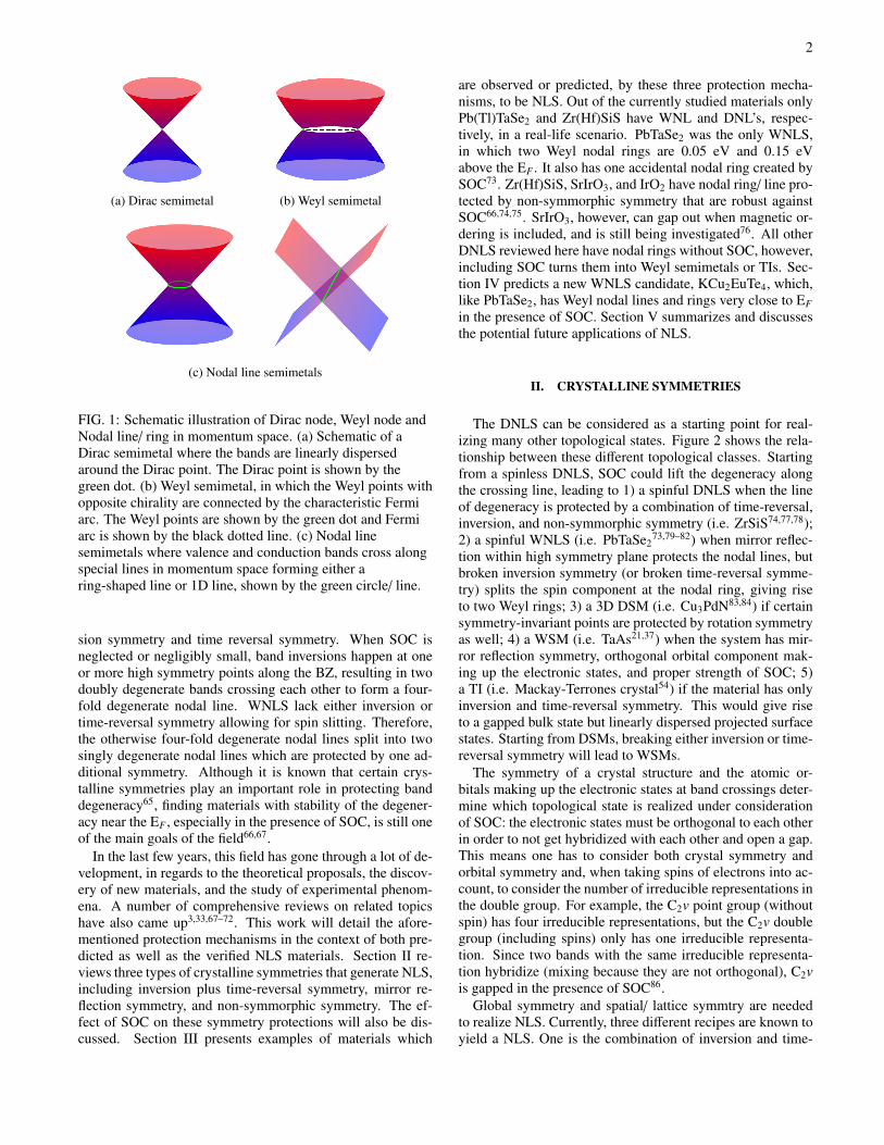
The DNLS can be considered as a starting point for real-izing many other topological states. Figure 2 shows the rela-tionship between these different topological classes. Startingfrom a spinless DNLS, SOC could lift the degeneracy alongthe crossing line, leading to 1) a spinful DNLS when the lineof degeneracy is protected by a combination of time-reversal,inversion, and non-symmorphic symmetry (i.e. ZrSiS74,77,78);2) a spinful WNLS (i.e. PbTaSe2
73,79–82) when mirror reflec-tion within high symmetry plane protects the nodal lines, butbroken inversion symmetry (or broken time-reversal symme-try) splits the spin component at the nodal ring, giving riseto two Weyl rings; 3) a 3D DSM (i.e. Cu3PdN83,84) if certainsymmetry-invariant points are protected by rotation symmetryas well; 4) a WSM (i.e. TaAs21,37) when the system has mir-ror reflection symmetry, orthogonal orbital component mak-ing up the electronic states, and proper strength of SOC; 5)a TI (i.e. Mackay-Terrones crystal54) if the material has onlyinversion and time-reversal symmetry. This would give riseto a gapped bulk state but linearly dispersed projected surfacestates. Starting from DSMs, breaking either inversion or time-reversal symmetry will lead to WSMs.
The symmetry of a crystal structure and the atomic or-bitals making up the electronic states at band crossings deter-mine which topological state is realized under considerationof SOC: the electronic states must be orthogonal to each otherin order to not get hybridized with each other and open a gap.This means one has to consider both crystal symmetry andorbital symmetry and, when taking spins of electrons into ac-count, to consider the number of irreducible representations inthe double group. For example, the C2v point group (withoutspin) has four irreducible representations, but the C2v doublegroup (including spins) only has one irreducible representa-tion. Since two bands with the same irreducible representa-tion hybridize (mixing because they are not orthogonal), C2vis gapped in the presence of SOC86.
Global symmetry and spatial/ lattice symmtry are neededto realize NLS. Currently, three different recipes are known toyield a NLS. One is the combination of inversion and time-
3
FIG. 2: Schematic of different topological states and their relationship with each other. The symmetries in red (blue) captionindicate the global symmetry or spatial/ lattice symmetry elements need to be preserved (broken) to realize the new topologicalphase.*: The evolvement to Weyl semimetal require mirror reflection symmetry, atomic orbital components making up the bandsforming the nodal lines, as well as the proper strength of SOC. If the strength of SOC is too strong, the system turns into a fullygapped insulator85.
reversal symmetry. The second recipe is to introduce addi-tional mirror symmetry, where the degeneracy on the mir-ror plane is protected. The third recipe is to introduce non-symmorphic symmetry such as glide mirror or screw rotation.The non-symmorphic symmetry demands normally singly de-generate points to cross at certain doubly degenerate points atthe BZ zone boundary86,87. SOC plays different roles in threescenarios. In this section, these three recipes, as well as theeffect of SOC on them will be discussed.
A. Inversion and time-reversal symmetry
In the absence of SOC, a crystalline system with simultane-ous presence of time-reversal and inversion symmetries gen-erates a DNL in 3D83. In such case when the 3D block Hamil-tonian is invariant under inversion and time-reversal symme-try, inversion and time-reversal symmetry constrain the Berryphase (Φ) on a closed loop in momentum space (C) to satisfyΦ(C) = Φ(-C) and Φ(C) = Φ(−C)∗. A non-trivial loop, where
4
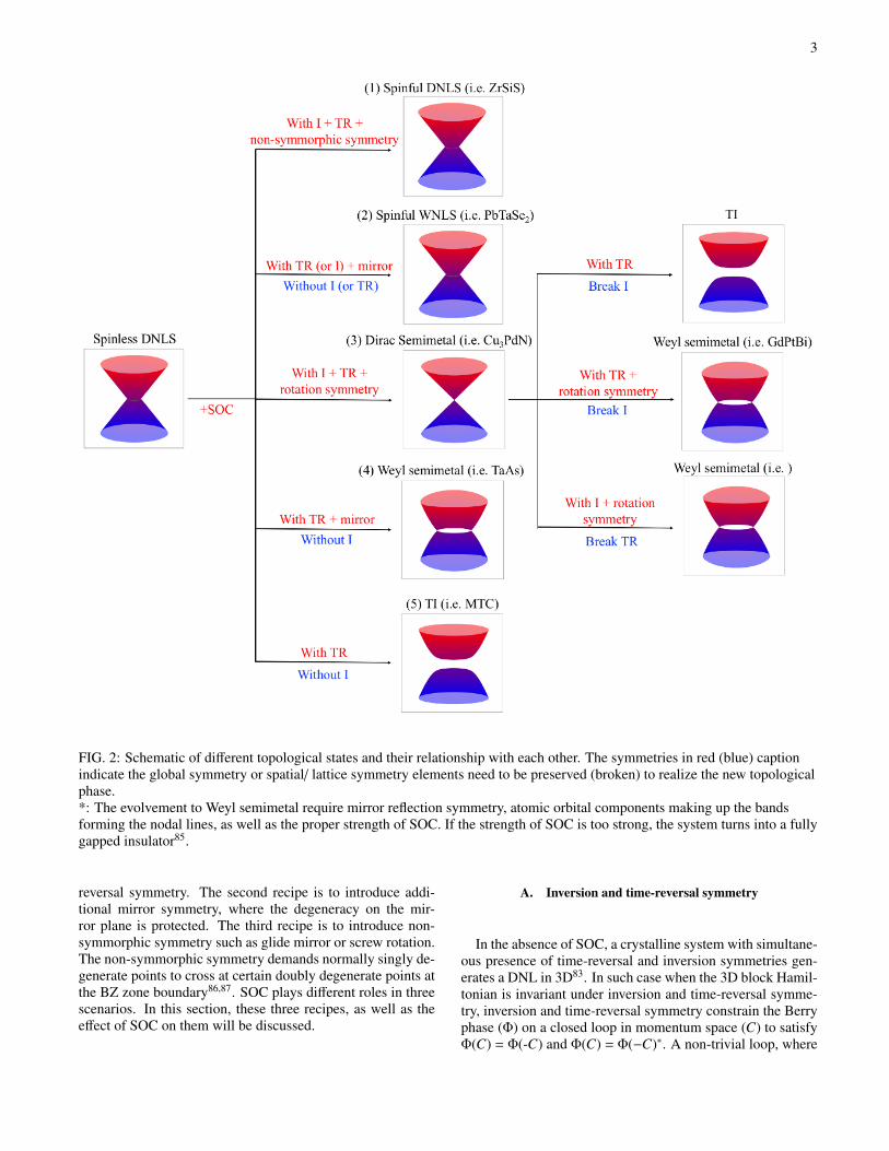
FIG. 3: Band folding in one-dimensional polymers. (a) Band structure of a polymer in which there are two atoms per unit cell.The bands contain two branches: one from the ‘running up’ bonding bands, and one from the ‘running down’ antibondingbands. The two branches intersect at k = π/(2a). (b) Band structure of a polymer in which there is one atom per unit cell. TheBZ is doubled because the unit cell is one half as it is in (a). (c) Production of band structure in (a) by folding band structure in(b). (d)-(e) Enlargement of the unit cell causes the multiplicity of bands. Bands are folded three times when the unit cell istripled, four times when quadrupled.
Φ(C) = -1, means that the loop contains a degeneracy. In 3D,this guarantees a small nodal loop at the band inversion83.
In the presence of SOC, Dirac crossings generated with thismechanism are, in general, gapped out owing to band repul-sion, unless the SOC is negligibly small, turning the systeminto a TI. However, if the system has an additional Cn, in par-ticular, C3, C4, and C6 rotation symmetries, the rotation sym-metry can protect the band crossing at certain generic discretepoints, turning the system into a DSM in the presence of SOC.Specifically, one has to consider the crystal structure and or-bital symmetry in a double group along the rotation axis. Ifthe electronic states along the rotation axis have different irre-ducible representations, rotation symmetry protects the Diracpoints on the axis. Everything else over the BZ is gapped, thusgiving rise to a 3D DSM in the SOC regime86.
B. Mirror reflection symmetry
When the mirror operation and the Hamiltonian commute,nodal rings can be generated and protected by mirror reflec-tion symmetry in the absence of SOC. For example, assuminga system described by Hamiltonian H(kx, ky, kz) has mirrorreflection Mxy, one has MH(kx, ky, -kz)M−1 = H(kx, ky, kz).In two high symmetry planes, kz = 0 and kz = π, the mirroroperation and the Hamiltonian commute. This makes them
simultaneously diagonalizable, resulting in oppositely signedmirror eigenvalues. Therefore, without SOC, these two bandsthat cross at the Dirac point are protected by the reflectionsymmetry from hybridizing with each other66,67,88,89.
Taking into account of SOC, depending on the atomic or-bitals making up the electronic states and the strength ofSOC, SOC can turn a spinless Dirac nodal rings into 1)a spinful Weyl nodal rings within the mirror planes (i.e.PbTaSe2
73,79–82). In this case, the WNLs are protected by mir-ror reflection symmetry; 2) a Weyl semimetal which has Weylpoints off the mirror planes (i.e. TaAs21,37). These Weyl pointsare completely accidental, highly depends on the strength ofSOC, and are no longer a result of mirror symmetry. 3) a TIwhen the strength of SOC is strong enough (i.e. CaAgAs85,89).
C. Non-symmorhpic symmetry
To understand how non-symmorphic symmetry generates aNLS, it is important to first understand how more than oneelectronic unit in a unit cell, or the choice of unit cell, resultsin band folding. The following explanation was first laid outby Hoffman et al90,91. Consider a 1D chain of molecules, onecan either see it as a polymer with one atom per unit cell, ortwice as many atoms per unit cell. Constructing the orbitals ofthe polymer with two different unit cells, when the polymer is
5
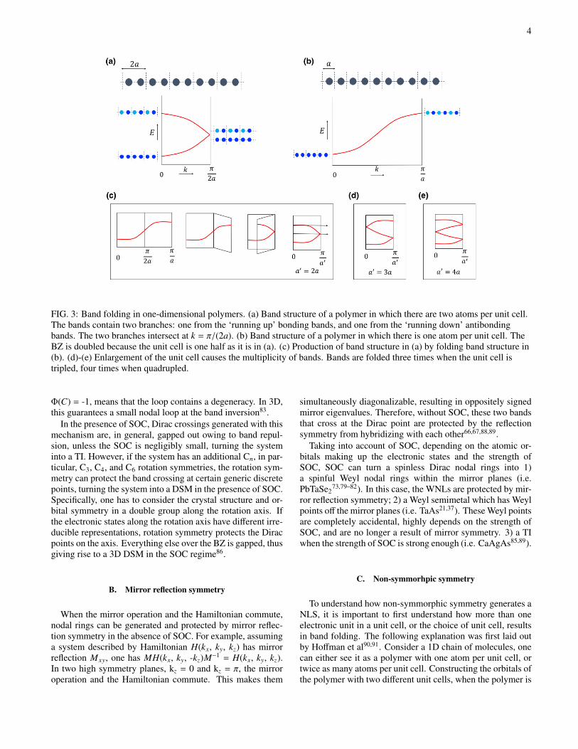
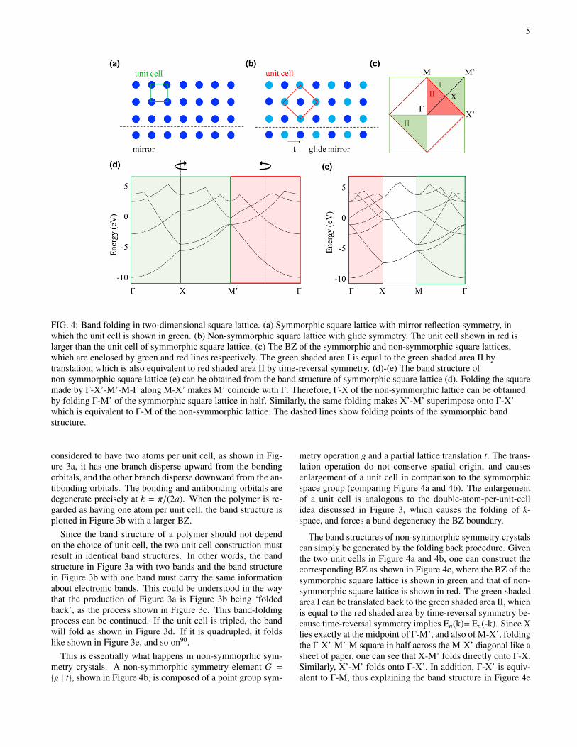
FIG. 4: Band folding in two-dimensional square lattice. (a) Symmorphic square lattice with mirror reflection symmetry, inwhich the unit cell is shown in green. (b) Non-symmorphic square lattice with glide symmetry. The unit cell shown in red islarger than the unit cell of symmorphic square lattice. (c) The BZ of the symmorphic and non-symmorphic square lattices,which are enclosed by green and red lines respectively. The green shaded area I is equal to the green shaded area II bytranslation, which is also equivalent to red shaded area II by time-reversal symmetry. (d)-(e) The band structure ofnon-symmorphic square lattice (e) can be obtained from the band structure of symmorphic square lattice (d). Folding the squaremade by Γ-X’-M’-M-Γ along M-X’ makes M’ coincide with Γ. Therefore, Γ-X of the non-symmorphic lattice can be obtainedby folding Γ-M’ of the symmorphic square lattice in half. Similarly, the same folding makes X’-M’ superimpose onto Γ-X’which is equivalent to Γ-M of the non-symmorphic lattice. The dashed lines show folding points of the symmorphic bandstructure.
considered to have two atoms per unit cell, as shown in Fig-ure 3a, it has one branch disperse upward from the bondingorbitals, and the other branch disperse downward from the an-tibonding orbitals. The bonding and antibonding orbitals aredegenerate precisely at k = π/(2a). When the polymer is re-garded as having one atom per unit cell, the band structure isplotted in Figure 3b with a larger BZ.
Since the band structure of a polymer should not dependon the choice of unit cell, the two unit cell construction mustresult in identical band structures. In other words, the bandstructure in Figure 3a with two bands and the band structurein Figure 3b with one band must carry the same informationabout electronic bands. This could be understood in the waythat the production of Figure 3a is Figure 3b being ‘foldedback’, as the process shown in Figure 3c. This band-foldingprocess can be continued. If the unit cell is tripled, the bandwill fold as shown in Figure 3d. If it is quadrupled, it foldslike shown in Figure 3e, and so on90.
This is essentially what happens in non-symmoprhic sym-metry crystals. A non-symmorphic symmetry element G =
{g | t}, shown in Figure 4b, is composed of a point group sym-
metry operation g and a partial lattice translation t. The trans-lation operation do not conserve spatial origin, and causesenlargement of a unit cell in comparison to the symmorphicspace group (comparing Figure 4a and 4b). The enlargementof a unit cell is analogous to the double-atom-per-unit-cellidea discussed in Figure 3, which causes the folding of k-space, and forces a band degeneracy the BZ boundary.
The band structures of non-symmorphic symmetry crystalscan simply be generated by the folding back procedure. Giventhe two unit cells in Figure 4a and 4b, one can construct thecorresponding BZ as shown in Figure 4c, where the BZ of thesymmorphic square lattice is shown in green and that of non-symmorphic square lattice is shown in red. The green shadedarea I can be translated back to the green shaded area II, whichis equal to the red shaded area by time-reversal symmetry be-cause time-reversal symmetry implies En(k)= En(-k). Since Xlies exactly at the midpoint of Γ-M’, and also of M-X’, foldingthe Γ-X’-M’-M square in half across the M-X’ diagonal like asheet of paper, one can see that X-M’ folds directly onto Γ-X.Similarly, X’-M’ folds onto Γ-X’. In addition, Γ-X’ is equiv-alent to Γ-M, thus explaining the band structure in Figure 4e
6
as a simple folding of Figure 4d91. In particular, Γ-X of thenon-symmorphic square can be constructed by folding Γ-M’of the symmorphic square lattice in half, and Γ-M (which isequivalent to Γ-X’) of the non-symmorphic square can be con-structed by the superposition (caused by the folding) of Γ-X’and X’-M’ of the symmorphic square lattice91.
What is interesting about the non-symmorphic protectednodal lines is that they cannot be gapped by SOC becausethey are protected by a lattice translation87. Take glide mir-ror as an example, since the translation t is a fraction of aprimitive unit vector, in spinless systems for Bloch states atk, G2 = e−ik·t. Therefore, the glide eigenvalues are ±e−ik·t/2.Considering spins, the glide eigenvalues are ±ie−ik·t/2. Eitherwith or without SOC, the non-symmorphic symmetry givetwo distinct eigenvalues, therefore the bands are protectedfrom being hybridized88.
III. MATERIAL REALIZATION
A. Time-reversal and inversion symmetry protected nodal linematerials
Centrosymmetric materials have inversion symmetry. Iftime-reversal symmetry is also presence in the system, four-fold degeneracies along nodal rings can be realized. Nodalrings created in this way generally exist only in the limit ofvanishing SOC. Including SOC typically turns the DNLS intoeither a DSM or a TI. Some predicted centrosymmetric DNLmaterials include cubic antiperovskite materials Cu3NX83,84,CaTe92, LaX93, Ca3P2
94, CaP3 family95, BaSn296,97, AlB2-
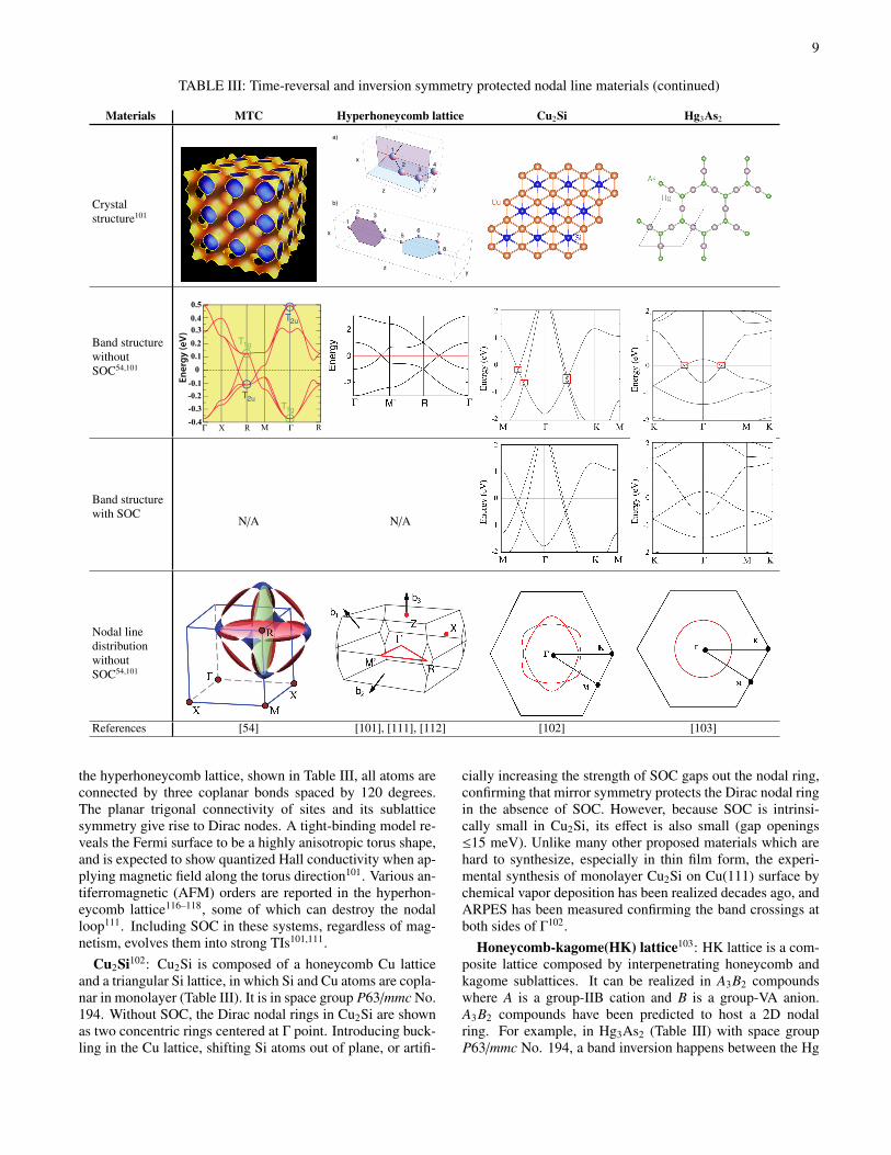
type diborides98–100, and 3D carbon allotrope materials withnegligible SOC such as Mackay-Terrones crystals54 and hy-perhoneycomb lattices101. In addition, two-dimensional DNLmaterials have also been proposed in monolayer Cu2Si102 andhoneycomb-kagome lattice103.
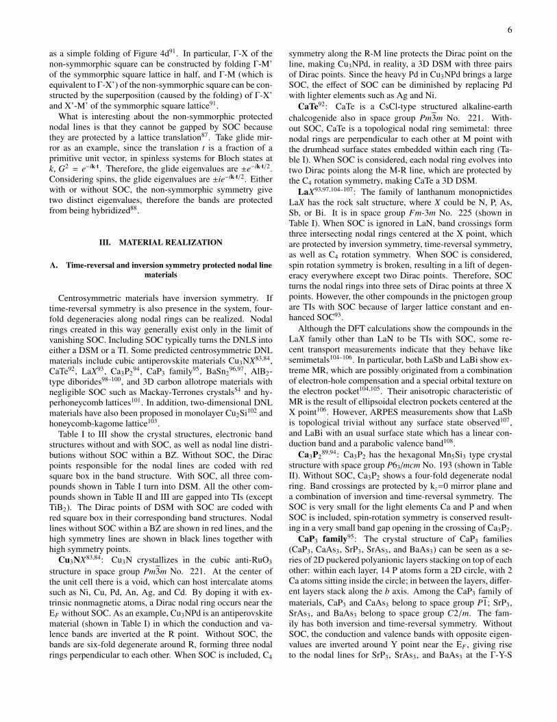
Table I to III show the crystal structures, electronic bandstructures without and with SOC, as well as nodal line distri-butions without SOC within a BZ. Without SOC, the Diracpoints responsible for the nodal lines are coded with redsquare box in the band structure. With SOC, all three com-pounds shown in Table I turn into DSM. All the other com-pounds shown in Table II and III are gapped into TIs (exceptTiB2). The Dirac points of DSM with SOC are coded withred square box in their corresponding band structures. Nodallines without SOC within a BZ are shown in red lines, and thehigh symmetry lines are shown in black lines together withhigh symmetry points.
Cu3NX83,84: Cu3N crystallizes in the cubic anti-RuO3
structure in space group Pm3m No. 221. At the center ofthe unit cell there is a void, which can host intercalate atomssuch as Ni, Cu, Pd, An, Ag, and Cd. By doping it with ex-trinsic nonmagnetic atoms, a Dirac nodal ring occurs near theEF without SOC. As an example, Cu3NPd is an antiperovskitematerial (shown in Table I) in which the conduction and va-lence bands are inverted at the R point. Without SOC, thebands are six-fold degenerate around R, forming three nodalrings perpendicular to each other. When SOC is included, C4
symmetry along the R-M line protects the Dirac point on theline, making Cu3NPd, in reality, a 3D DSM with three pairsof Dirac points. Since the heavy Pd in Cu3NPd brings a largeSOC, the effect of SOC can be diminished by replacing Pdwith lighter elements such as Ag and Ni.
CaTe92: CaTe is a CsCl-type structured alkaline-earthchalcogenide also in space group Pm3m No. 221. With-out SOC, CaTe is a topological nodal ring semimetal: threenodal rings are perpendicular to each other at M point withthe drumhead surface states embedded within each ring (Ta-ble I). When SOC is considered, each nodal ring evolves intotwo Dirac points along the M-R line, which are protected bythe C4 rotation symmetry, making CaTe a 3D DSM.
LaX93,97,104–107: The family of lanthanum monopnictidesLaX has the rock salt structure, where X could be N, P, As,Sb, or Bi. It is in space group Fm-3m No. 225 (shown inTable I). When SOC is ignored in LaN, band crossings formthree intersecting nodal rings centered at the X point, whichare protected by inversion symmetry, time-reversal symmetry,as well as C4 rotation symmetry. When SOC is considered,spin rotation symmetry is broken, resulting in a lift of degen-eracy everywhere except two Dirac points. Therefore, SOCturns the nodal rings into three sets of Dirac points at three Xpoints. However, the other compounds in the pnictogen groupare TIs with SOC because of larger lattice constant and en-hanced SOC93.
Although the DFT calculations show the compounds in theLaX family other than LaN to be TIs with SOC, some re-cent transport measurements indicate that they behave likesemimetals104–106. In particular, both LaSb and LaBi show ex-treme MR, which are possibly originated from a combinationof electron-hole compensation and a special orbital texture onthe electron pocket104,105. Their anisotropic characteristic ofMR is the result of ellipsoidal electron pockets centered at theX point106. However, ARPES measurements show that LaSbis topological trivial without any surface state observed107,and LaBi with an usual surface state which has a linear con-duction band and a parabolic valence band108.
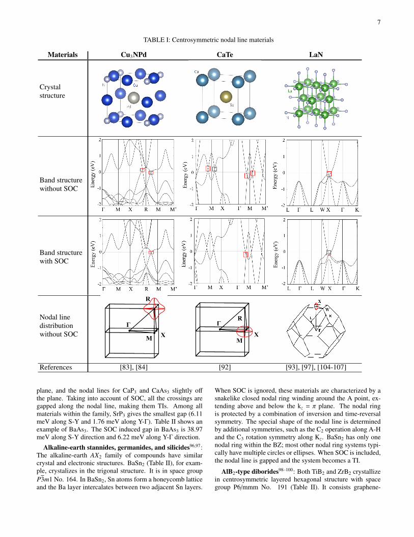
Ca3P289,94: Ca3P2 has the hexagonal Mn5Si3 type crystal
structure with space group P63/mcm No. 193 (shown in TableII). Without SOC, Ca3P2 shows a four-fold degenerate nodalring. Band crossings are protected by kz=0 mirror plane anda combination of inversion and time-reversal symmetry. TheSOC is very small for the light elements Ca and P and whenSOC is included, spin-rotation symmetry is conserved result-ing in a very small band gap opening in the crossing of Ca3P2.
CaP3 family95: The crystal structure of CaP3 families(CaP3, CaAs3, SrP3, SrAs3, and BaAs3) can be seen as a se-ries of 2D puckered polyanionic layers stacking on top of eachother: within each layer, 14 P atoms form a 2D circle, with 2Ca atoms sitting inside the circle; in between the layers, differ-ent layers stack along the b axis. Among the CaP3 family ofmaterials, CaP3 and CaAs3 belong to space group P1; SrP3,SrAs3, and BaAs3 belong to space group C2/m. The fam-ily has both inversion and time-reversal symmetry. WithoutSOC, the conduction and valence bands with opposite eigen-values are inverted around Y point near the EF , giving riseto the nodal lines for SrP3, SrAs3, and BaAs3 at the Γ-Y-S
7
TABLE I: Centrosymmetric nodal line materials
Materials Cu3NPd CaTe LaN
Crystalstructure
Band structurewithout SOC
Band structurewith SOC
Nodal linedistributionwithout SOC
References [83], [84] [92] [93], [97], [104-107]
plane, and the nodal lines for CaP3 and CaAs3 slightly off
the plane. Taking into account of SOC, all the crossings aregapped along the nodal line, making them TIs. Among allmaterials within the family, SrP3 gives the smallest gap (6.11meV along S-Y and 1.76 meV along Y-Γ). Table II shows anexample of BaAs3. The SOC induced gap in BaAs3 is 38.97meV along S-Y direction and 6.22 meV along Y-Γ direction.
Alkaline-earth stannides, germanides, and silicides96,97:The alkaline-earth AX2 family of compounds have similarcrystal and electronic structures. BaSn2 (Table II), for exam-ple, crystalizes in the trigonal structure. It is in space groupP3m1 No. 164. In BaSn2, Sn atoms form a honeycomb latticeand the Ba layer intercalates between two adjacent Sn layers.
When SOC is ignored, these materials are characterized by asnakelike closed nodal ring winding around the A point, ex-tending above and below the kz = π plane. The nodal ringis protected by a combination of inversion and time-reversalsymmetry. The special shape of the nodal line is determinedby additional symmetries, such as the C2 operation along A-Hand the C3 rotation symmetry along Kz. BaSn2 has only onenodal ring within the BZ; most other nodal ring systems typi-cally have multiple circles or ellipses. When SOC is included,the nodal line is gapped and the system becomes a TI.
AlB2-type diborides98–100: Both TiB2 and ZrB2 crystallizein centrosymmetric layered hexagonal structure with spacegroup P6/mmm No. 191 (Table II). It consists graphene-
8
TABLE II: Time-reversal and inversion symmetry protected nodal line materials (continued)
Materials Ca3P2 BaAs3 BaSn2 TiB2
Crystalstructure
Band structurewithout SOC
Band structurewith SOC
Nodal linedistributionwithout SOC
References [89], [94] [95] [96], [97] [98-100]
like boron layers and alternating hexagonal titanium or zir-conium layers. Both compounds have been successfully syn-thesized in laboratory, and have brought much interests owingto the unique combination of properties such as high melt-ing point, high bonding strength, high thermal and electricalconductivity109,110.
Some electronic properties of the AlB2 diborides are em-bedded in their band structures, such as a nodal net structureincluding triple point, nexus, and nodal link98,99. Take TiB2 asan example, without SOC, six band crossings emerge aroundthe EF , along the H-Γ, Γ-A, A-H, K-Γ, M-K, and L-A direc-tions. These band crossings give rise to four different kindsof nodal line structures, including 1) a nodal ring in the Mxyplane centered around K point100; 2) a nodal ring in the in theMxy plane centered around A point; 3) nodal lines in threevertical mirror planes σv1, σv2, and σv3; 4) nodal line alongΓ-A starting from a triple point. All the four classes of nodallines together compose a complex nodal net structure. In thepresence of SOC, all the crossings except the one along Γ-Aare gapped out, with the gap size ranging from 18 meV to 26
meV. SOC also generates a new Dirac point along Γ-A.
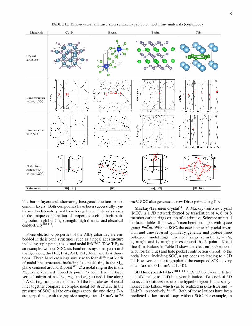
Mackay-Terrones crystal54: A Mackay-Terrones crystal(MTC) is a 3D network formed by tessellation of 4, 6, or 8member carbon rings on top of a primitive Schwarz minimalsurface. Table III shows a 6-membered example with spacegroup Pm3m. Without SOC, the coexistence of spacial inver-sion and time-reversal symmetry generate and protect threeorthogonal nodal rings. The nodal rings are in the kx = π/a,ky = π/a, and kz = π/a planes around the R point. Nodalline distributions in Table II show the electron pockets con-tribution (in blue) and hole pocket contribution (in red) to thenodal lines. Including SOC, a gap opens up leading to a 3DTI. However, similar to graphene, the computed SOC is verysmall (around 0.13 meV at 1.5 K).
3D Honeycomb lattice101,111,112: A 3D honeycomb latticeis a 3D analog to a 2D honeycomb lattice. Two typical 3Dhoneycomb lattices include the hyperhoneycomb and stripy-honeycomb lattice, which can be realized in β-Li2IrO3 and γ-Li2IrO3, respectively113–115. Both of these lattices have beenpredicted to host nodal loops without SOC. For example, in
9
TABLE III: Time-reversal and inversion symmetry protected nodal line materials (continued)
Materials MTC Hyperhoneycomb lattice Cu2Si Hg3As2
Crystalstructure101
1
23
4x
z
1
23
45
67
8
x
z
b)
y
a)
y
Band structurewithoutSOC54,101
-0.4
-0.3
-0.2
-0.1
0
0.1
0.2
0.3
0.4
0.5
Γ X M Γ R
En
erg
y (
eV
)
R
T2u
T1g
T2u
T1g
Band structurewith SOC
N/A N/A
Nodal linedistributionwithoutSOC54,101
References [54] [101], [111], [112] [102] [103]
the hyperhoneycomb lattice, shown in Table III, all atoms areconnected by three coplanar bonds spaced by 120 degrees.The planar trigonal connectivity of sites and its sublatticesymmetry give rise to Dirac nodes. A tight-binding model re-veals the Fermi surface to be a highly anisotropic torus shape,and is expected to show quantized Hall conductivity when ap-plying magnetic field along the torus direction101. Various an-tiferromagnetic (AFM) orders are reported in the hyperhon-eycomb lattice116–118, some of which can destroy the nodalloop111. Including SOC in these systems, regardless of mag-netism, evolves them into strong TIs101,111.
Cu2Si102: Cu2Si is composed of a honeycomb Cu latticeand a triangular Si lattice, in which Si and Cu atoms are copla-nar in monolayer (Table III). It is in space group P63/mmc No.194. Without SOC, the Dirac nodal rings in Cu2Si are shownas two concentric rings centered at Γ point. Introducing buck-ling in the Cu lattice, shifting Si atoms out of plane, or artifi-
cially increasing the strength of SOC gaps out the nodal ring,confirming that mirror symmetry protects the Dirac nodal ringin the absence of SOC. However, because SOC is intrinsi-cally small in Cu2Si, its effect is also small (gap openings≤15 meV). Unlike many other proposed materials which arehard to synthesize, especially in thin film form, the experi-mental synthesis of monolayer Cu2Si on Cu(111) surface bychemical vapor deposition has been realized decades ago, andARPES has been measured confirming the band crossings atboth sides of Γ102.
Honeycomb-kagome(HK) lattice103: HK lattice is a com-posite lattice composed by interpenetrating honeycomb andkagome sublattices. It can be realized in A3B2 compoundswhere A is a group-IIB cation and B is a group-VA anion.A3B2 compounds have been predicted to host a 2D nodalring. For example, in Hg3As2 (Table III) with space groupP63/mmc No. 194, a band inversion happens between the Hg
10
s-orbital and the As pz-orbital without SOC. With respect toxy mirror plane, the eigenstates of two bands have same paritybut opposite eigenvalues, therefore resulting in a band inver-sion. In the presence of SOC, the nodal ring turns into a 2DTI, which has been confirmed by the existence of nontrivialhelical edge states103.
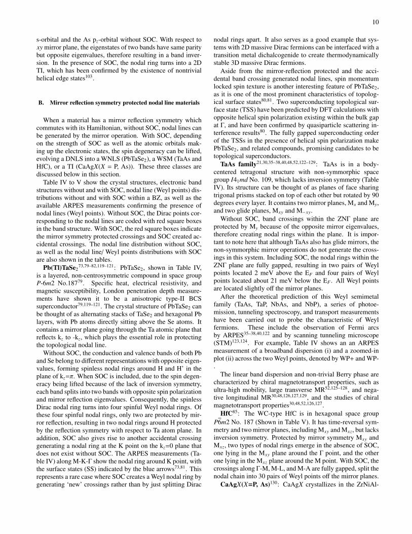
B. Mirror reflection symmetry protected nodal line materials
When a material has a mirror reflection symmetry whichcommutes with its Hamiltonian, without SOC, nodal lines canbe generated by the mirror operation. With SOC, dependingon the strength of SOC as well as the atomic orbitals mak-ing up the electronic states, the spin degeneracy can be lifted,evolving a DNLS into a WNLS (PbTaSe2), a WSM (TaAs andHfC), or a TI (CaAgX(X = P, As)). These three classes arediscussed below in this section.
Table IV to V show the crystal structures, electronic bandstructures without and with SOC, nodal line (Weyl points) dis-tributions without and with SOC within a BZ, as well as theavailable ARPES measurements confirming the presence ofnodal lines (Weyl points). Without SOC, the Dirac points cor-responding to the nodal lines are coded with red square boxesin the band structure. With SOC, the red square boxes indicatethe mirror symmetry protected crossings and SOC created ac-cidental crossings. The nodal line distribution without SOC,as well as the nodal line/ Weyl points distributions with SOCare also shown in the tables.
Pb(Tl)TaSe273,79–82,119–121: PbTaSe2, shown in Table IV,
is a layered, non-centrosymmetric compound in space groupP-6m2 No.18779. Specific heat, electrical resistivity, andmagnetic susceptibility, London penetration depth measure-ments have shown it to be a anisotropic type-II BCSsuperconductor79,119–121. The crystal structure of PbTaSe2 canbe thought of as alternating stacks of TaSe2 and hexagonal Pblayers, with Pb atoms directly sitting above the Se atoms. Itcontains a mirror plane going through the Ta atomic plane thatreflects kz to -kz, which plays the essential role in protectingthe topological nodal line.
Without SOC, the conduction and valence bands of both Pband Se belong to different representations with opposite eigen-values, forming spinless nodal rings around H and H’ in theplane of kz=π. When SOC is included, due to the spin degen-eracy being lifted because of the lack of inversion symmetry,each band splits into two bands with opposite spin polarizationand mirror reflection eigenvalues. Consequently, the spinlessDirac nodal ring turns into four spinful Weyl nodal rings. Ofthese four spinful nodal rings, only two are protected by mir-ror reflection, resulting in two nodal rings around H protectedby the reflection symmetry with respect to Ta atom plane. Inaddition, SOC also gives rise to another accidental crossinggenerating a nodal ring at the K point on the kz=0 plane thatdoes not exist without SOC. The ARPES measurements (Ta-ble IV) along M-K-Γ show the nodal ring around K point, withthe surface states (SS) indicated by the blue arrows73,81. Thisrepresents a rare case where SOC creates a Weyl nodal ring bygenerating ‘new’ crossings rather than by just splitting Dirac
nodal rings apart. It also serves as a good example that sys-tems with 2D massive Dirac fermions can be interfaced with atransition metal dichalcogenide to create thermodynamicallystable 3D massive Dirac fermions.
Aside from the mirror-reflection protected and the acci-dental band crossing generated nodal lines, spin momentumlocked spin texture is another interesting feature of PbTaSe2,as it is one of the most prominent characteristics of topolog-ical surface states80,81. Two superconducting topological sur-face state (TSS) have been predicted by DFT calculations withopposite helical spin polarization existing within the bulk gapat Γ, and have been confirmed by quasiparticle scattering in-terference results80. The fully gapped superconducting orderof the TSSs in the presence of helical spin polarization makePbTaSe2, and related compounds, promising candidates to betopological superconductors.
TaAs family21,30,35–38,40,48,52,122–129: TaAs is in a body-centered tetragonal structure with non-symmorphic spacegroup I41md No. 109, which lacks inversion symmetry (TableIV). Its structure can be thought of as planes of face sharingtrigonal prisms stacked on top of each other but rotated by 90degrees every layer. It contains two mirror planes, Mx and My,and two glide planes, Mxy and M−xy.
Without SOC, band crossings within the ZNΓ plane areprotected by My because of the opposite mirror eigenvalues,therefore creating nodal rings within the plane. It is impor-tant to note here that although TaAs also has glide mirrors, thenon-symmorphic mirror operations do not generate the cross-ings in this system. Including SOC, the nodal rings within theZNΓ plane are fully gapped, resulting in two pairs of Weylpoints located 2 meV above the EF and four pairs of Weylpoints located about 21 meV below the EF . All Weyl pointsare located slightly off the mirror planes.
After the theoretical prediction of this Weyl semimetalfamily (TaAs, TaP, NbAs, and NbP), a series of photoe-mission, tunneling spectroscopy, and transport measurementshave been carried out to probe the characteristic of Weylfermions. These include the observation of Fermi arcsby ARPES35–38,40,122 and by scanning tunneling microscope(STM)123,124. For example, Table IV shows an an ARPESmeasurement of a broadband dispersion (i) and a zoomed-inplot (ii) across the two Weyl points, denoted by WP+ and WP-.
The linear band dispersion and non-trivial Berry phase arecharacterized by chiral magnetotransport properties, such asultra-high mobility, large transverse MR52,125–128, and nega-tive longitudinal MR30,48,126,127,129, and the studies of chiralmagnetotransport properties30,48,52,126,127.
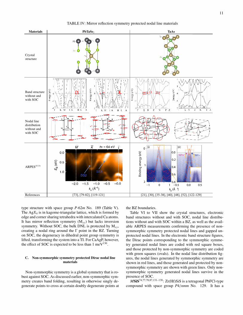
HfC85: The WC-type HfC is in hexagonal space groupP6m2 No. 187 (Shown in Table V). It has time-reversal sym-metry and two mirror planes, including Mxy and Mxz, but lacksinversion symmetry. Protected by mirror symmetry Mxy andMxz, two types of nodal rings emerge in the absence of SOC,one lying in the Mxy plane around the Γ point, and the otherone lying in the Mxz plane around the M point. With SOC, thecrossings along Γ-M, M-L, and M-A are fully gapped, split thenodal chain into 30 pairs of Weyl points off the mirror planes.
CaAgX(X=P, As)130: CaAgX crystallizes in the ZrNiAl-
11
TABLE IV: Mirror reflection symmetry protected nodal line materials
Materials PbTaSe2 TaAs
Crystalstructure
Band structurewithout andwith SOC
Nodal linedistributionwithout andwith SOC
ARPES37,73
References [73], [79-82], [119-121] [21], [30], [35-38], [40], [48], [52], [122-129]
type structure with space group P-62m No. 189 (Table V).The AgX4 is in kagome-triangular lattice, which is formed byedge and corner sharing tetrahedra with intercalated Ca atoms.It has mirror reflection symmetry (Mxy) but lacks inversionsymmetry. Without SOC, the bulk DNL is protected by Mxy,creating a nodal ring around the Γ point in the BZ. Turningon SOC, the degeneracy in dihedral point group symmetry islifted, transforming the system into a TI. For CaAgP, however,the effect of SOC is expected to be less than 1 meV130.
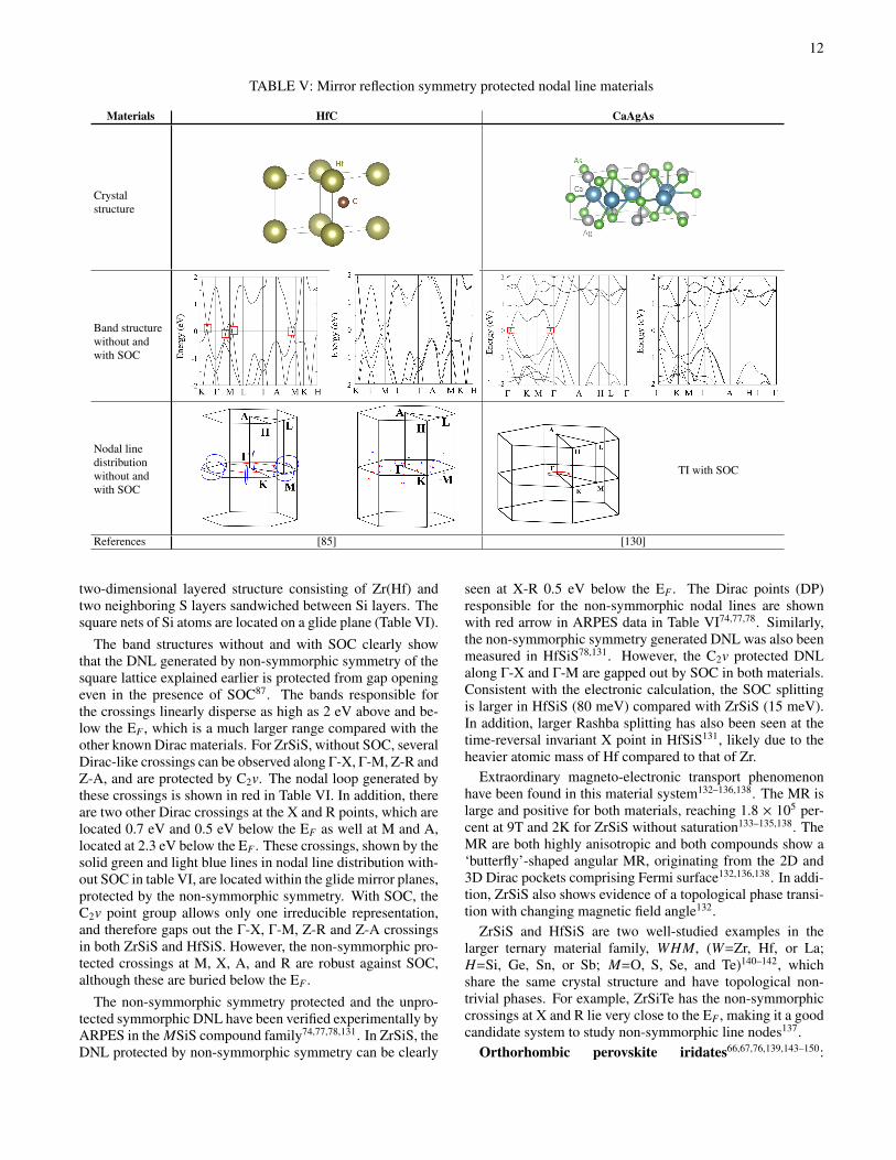
C. Non-symmorphic symmetry protected Dirac nodal linematerials
Non-symmorphic symmetry is a global symmetry that is ro-bust against SOC. As discussed earlier, non-symmorphic sym-metry creates band folding, resulting in otherwise singly de-generate points to cross at certain doubly degenerate points at
the BZ boundaries.Table VI to VII show the crystal structures, electronic
band structures without and with SOC, nodal line distribu-tions without and with SOC within a BZ, as well as the avail-able ARPES measurements confirming the presence of non-symmorphic symmetry protected nodal lines and gapped un-protected nodal lines. In the electronic band structure figures,the Dirac points corresponding to the symmorphic symme-try generated nodal lines are coded with red square boxes,and those protected by non-symmorphic symmetry are codedwith green squares (ovals). In the nodal line distribution fig-ures, the nodal lines generated by symmorphic symmetry areshown in red lines, and those generated and protected by non-symmorphic symmetry are shown with green lines. Only non-symmorphic symmetry generated nodal lines survive in thepresence of SOC.
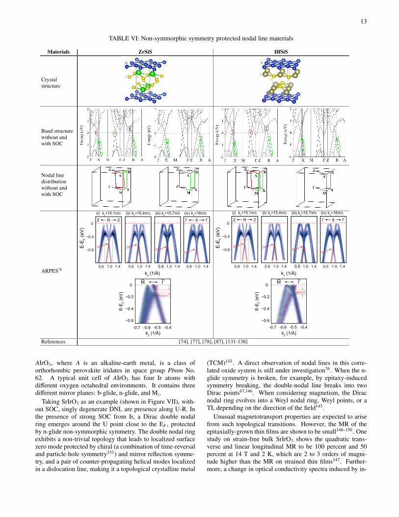
MSiS74,77,78,87,131–138: Zr(Hf)SiS is a tetragonal PbFCl-typecompound with space group P4/nmm No. 129. It has a
12
TABLE V: Mirror reflection symmetry protected nodal line materials
Materials HfC CaAgAs
Crystalstructure
Band structurewithout andwith SOC
Nodal linedistributionwithout andwith SOC
TI with SOC
References [85] [130]
two-dimensional layered structure consisting of Zr(Hf) andtwo neighboring S layers sandwiched between Si layers. Thesquare nets of Si atoms are located on a glide plane (Table VI).
The band structures without and with SOC clearly showthat the DNL generated by non-symmorphic symmetry of thesquare lattice explained earlier is protected from gap openingeven in the presence of SOC87. The bands responsible forthe crossings linearly disperse as high as 2 eV above and be-low the EF , which is a much larger range compared with theother known Dirac materials. For ZrSiS, without SOC, severalDirac-like crossings can be observed along Γ-X, Γ-M, Z-R andZ-A, and are protected by C2v. The nodal loop generated bythese crossings is shown in red in Table VI. In addition, thereare two other Dirac crossings at the X and R points, which arelocated 0.7 eV and 0.5 eV below the EF as well at M and A,located at 2.3 eV below the EF . These crossings, shown by thesolid green and light blue lines in nodal line distribution with-out SOC in table VI, are located within the glide mirror planes,protected by the non-symmorphic symmetry. With SOC, theC2v point group allows only one irreducible representation,and therefore gaps out the Γ-X, Γ-M, Z-R and Z-A crossingsin both ZrSiS and HfSiS. However, the non-symmorphic pro-tected crossings at M, X, A, and R are robust against SOC,although these are buried below the EF .
The non-symmorphic symmetry protected and the unpro-tected symmorphic DNL have been verified experimentally byARPES in the MSiS compound family74,77,78,131. In ZrSiS, theDNL protected by non-symmorphic symmetry can be clearly
seen at X-R 0.5 eV below the EF . The Dirac points (DP)responsible for the non-symmorphic nodal lines are shownwith red arrow in ARPES data in Table VI74,77,78. Similarly,the non-symmorphic symmetry generated DNL was also beenmeasured in HfSiS78,131. However, the C2v protected DNLalong Γ-X and Γ-M are gapped out by SOC in both materials.Consistent with the electronic calculation, the SOC splittingis larger in HfSiS (80 meV) compared with ZrSiS (15 meV).In addition, larger Rashba splitting has also been seen at thetime-reversal invariant X point in HfSiS131, likely due to theheavier atomic mass of Hf compared to that of Zr.
Extraordinary magneto-electronic transport phenomenonhave been found in this material system132–136,138. The MR islarge and positive for both materials, reaching 1.8 × 10⁵ per-cent at 9T and 2K for ZrSiS without saturation133–135,138. TheMR are both highly anisotropic and both compounds show a‘butterfly’-shaped angular MR, originating from the 2D and3D Dirac pockets comprising Fermi surface132,136,138. In addi-tion, ZrSiS also shows evidence of a topological phase transi-tion with changing magnetic field angle132.
ZrSiS and HfSiS are two well-studied examples in thelarger ternary material family, WHM, (W=Zr, Hf, or La;H=Si, Ge, Sn, or Sb; M=O, S, Se, and Te)140–142, whichshare the same crystal structure and have topological non-trivial phases. For example, ZrSiTe has the non-symmorphiccrossings at X and R lie very close to the EF , making it a goodcandidate system to study non-symmorphic line nodes137.
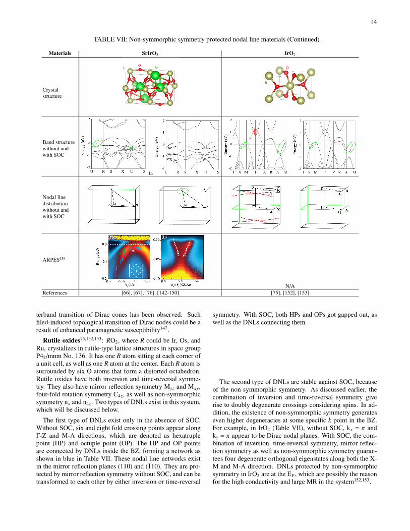
Orthorhombic perovskite iridates66,67,76,139,143–150:
13
TABLE VI: Non-symmorphic symmetry protected nodal line materials
Materials ZrSiS HfSiS
Crystalstructure
Band structurewithout andwith SOC
Nodal linedistributionwithout andwith SOC
ARPES78
References [74], [77], [78], [87], [131-138]
AIrO3, where A is an alkaline-earth metal, is a class oforthorhombic perovskite iridates in space group Pbnm No.62. A typical unit cell of AIrO3 has four Ir atoms withdifferent oxygen octahedral environments. It contains threedifferent mirror planes: b-glide, n-glide, and Mz.
Taking SrIrO3 as an example (shown in Figure VII), with-out SOC, singly degenerate DNL are presence along U-R. Inthe presence of strong SOC from Ir, a Dirac double nodalring emerges around the U point close to the EF , protectedby n-glide non-symmorphic symmetry. The double nodal ringexhibits a non-trivial topology that leads to localized surfacezero mode protected by chiral (a combination of time-reversaland particle-hole symmetry151) and mirror reflection symme-try, and a pair of counter-propagating helical modes localizedin a dislocation line, making it a topological crystalline metal
(TCM)143. A direct observation of nodal lines in this corre-lated oxide system is still under investigation76. When the n-glide symmetry is broken, for example, by epitaxy-inducedsymmetry breaking, the double-nodal line breaks into twoDirac points67,146. When considering magnetism, the Diracnodal ring evolves into a Weyl nodal ring, Weyl points, or aTI, depending on the direction of the field143.
Unusual magnetotransport properties are expected to arisefrom such topological transitions. However, the MR of theepitaxially-grown thin films are shown to be small148–150. Onestudy on strain-free bulk SrIrO3 shows the quadratic trans-verse and linear longitudinal MR to be 100 percent and 50percent at 14 T and 2 K, which are 2 to 3 orders of magni-tude higher than the MR on strained thin films147. Further-more, a change in optical conductivity spectra induced by in-
14
TABLE VII: Non-symmorphic symmetry protected nodal line materials (Continued)
Materials SrIrO3 IrO2
Crystalstructure
Band structurewithout andwith SOC
ta
Nodal linedistributionwithout andwith SOC
ARPES139
N/AReferences [66], [67], [76], [142-150] [75], [152], [153]
terband transition of Dirac cones has been observed. Suchfiled-induced topological transition of Dirac nodes could be aresult of enhanced paramagnetic susceptibility147.
Rutile oxides75,152,153: RO2, where R could be Ir, Os, andRu, crystalizes in rutile-type lattice structures in space groupP42/mnm No. 136. It has one R atom sitting at each corner ofa unit cell, as well as one R atom at the center. Each R atom issurrounded by six O atoms that form a distorted octahedron.Rutile oxides have both inversion and time-reversal symme-try. They also have mirror reflection symmetry Myz and Mxy,four-fold rotation symmetry C4z, as well as non-symmorphicsymmetry nx and n4z. Two types of DNLs exist in this system,which will be discussed below.
The first type of DNLs exist only in the absence of SOC.Without SOC, six and eight fold crossing points appear alongΓ-Z and M-A directions, which are denoted as hexatruplepoint (HP) and octuple point (OP). The HP and OP pointsare connected by DNLs inside the BZ, forming a network asshown in blue in Table VII. These nodal line networks existin the mirror reflection planes (110) and (110). They are pro-tected by mirror reflection symmetry without SOC, and can betransformed to each other by either inversion or time-reversal
symmetry. With SOC, both HPs and OPs got gapped out, aswell as the DNLs connecting them.
The second type of DNLs are stable against SOC, becauseof the non-symmorphic symmetry. As discussed earlier, thecombination of inversion and time-reversal symmetry giverise to doubly degenerate crossings considering spins. In ad-dition, the existence of non-symmorphic symmetry generateseven higher degeneracies at some specific k point in the BZ.For example, in IrO2 (Table VII), without SOC, kx = π andky = π appear to be Dirac nodal planes. With SOC, the com-bination of inversion, time-reversal symmetry, mirror reflec-tion symmetry as well as non-symmorphic symmetry guaran-tees four degenerate orthogonal eigenstates along both the X-M and M-A direction. DNLs protected by non-symmorphicsymmetry in IrO2 are at the EF , which are possibly the reasonfor the high conductivity and large MR in the system152,153.
15
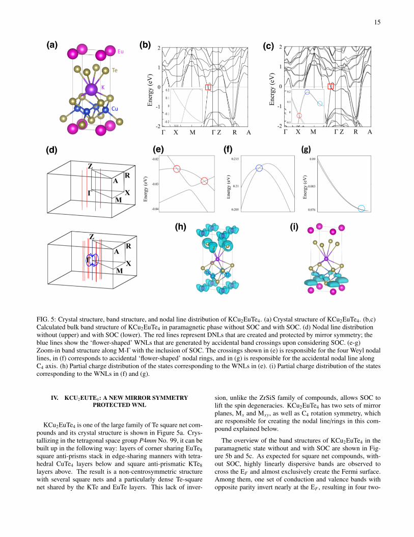
FIG. 5: Crystal structure, band structure, and nodal line distribution of KCu2EuTe4. (a) Crystal structure of KCu2EuTe4. (b,c)Calculated bulk band structure of KCu2EuTe4 in paramagnetic phase without SOC and with SOC. (d) Nodal line distributionwithout (upper) and with SOC (lower). The red lines represent DNLs that are created and protected by mirror symmetry; theblue lines show the ‘flower-shaped’ WNLs that are generated by accidental band crossings upon considering SOC. (e-g)Zoom-in band structure along M-Γ with the inclusion of SOC. The crossings shown in (e) is responsible for the four Weyl nodallines, in (f) corresponds to accidental ‘flower-shaped’ nodal rings, and in (g) is responsible for the accidental nodal line alongC4 axis. (h) Partial charge distribution of the states corresponding to the WNLs in (e). (i) Partial charge distribution of the statescorresponding to the WNLs in (f) and (g).
IV. KCU2EUTE4: A NEW MIRROR SYMMETRYPROTECTED WNL
KCu2EuTe4 is one of the large family of Te square net com-pounds and its crystal structure is shown in Figure 5a. Crys-tallizing in the tetragonal space group P4mm No. 99, it can bebuilt up in the following way: layers of corner sharing EuTe8square anti-prisms stack in edge-sharing manners with tetra-hedral CuTe4 layers below and square anti-prismatic KTe8layers above. The result is a non-centrosymmetric structurewith several square nets and a particularly dense Te-squarenet shared by the KTe and EuTe layers. This lack of inver-
sion, unlike the ZrSiS family of compounds, allows SOC tolift the spin degeneracies. KCu2EuTe4 has two sets of mirrorplanes, Mx and Mxy, as well as C4 rotation symmetry, whichare responsible for creating the nodal line/rings in this com-pound explained below.
The overview of the band structures of KCu2EuTe4 in theparamagnetic state without and with SOC are shown in Fig-ure 5b and 5c. As expected for square net compounds, with-out SOC, highly linearly dispersive bands are observed tocross the EF and almost exclusively create the Fermi surface.Among them, one set of conduction and valence bands withopposite parity invert nearly at the EF , resulting in four two-
16
fold spinless DNL protected by Mxy mirror symmetry. Thedistribution of this set of nodal lines in the first BZ is shownin red in the upper panel of Figure 5d. The energy dispersionof these nodal lines are almost flat.
Upon introducing SOC, each band splits into two singly de-generate bands, giving rise to more band crossings in the Mxymirror plane. However, as noted earlier, only if the bands haveopposite eigenvalues (±i) under mirror operation are the bandcrossings maintained. In KCu2EuTe4, the spinless DNL splitsinto two spinful WNLs as shown in red in the lower panel ofFigure 5d. The band projections of these states show that theWNLs are attributed to both the Eu and Te sublattices, shownin Figure 5h. Similar to the inversion plus SOC generatednew crossing in PbTaSe2, SOC in KCu2EuTe4 also generatesa new accidental band crossing and a set of ‘flower-shaped’Weyl nodal rings in the Mxy plane, appearing above the EFshown in blue in the lower panel of Figure 5d. Band pro-jections show that mainly Eu sublattices contribute to thesestates (Figure 5i). A zoom-in view of the band between Mand G with SOC are shown in Figures 5e to 5g. Among them,the band structure shown in Figure 5e corresponds to the DNLsplit WNLs, Figure 5f corresponds to the crossing responsiblefor the ‘flower shaped’ nodal ring, and Figure 5g correspondsto inversion plus SOC newly generated nodal lines along theC4 rotation axis.
It is also worth mentioning that aside from the nodal linesand rings discussed above, more crossings both above and be-low the EF , within about 1 eV, are present, implying moreinteresting nodal lines/rings to be explored in this family ofcompounds. Tuning the EF and band structure via chemi-cal control, similar to the ZrSiS family, should be possible.To the best of our knowledge, KCu2EuTe4 is the first pre-dicted WNLS which have nodal lines almost exactly at theEF , making it a good candidate to study the exotic physicsrelated to WNLS. Transport and magnetic measurements byKanatzidis et al indicate KCu2EuTe4 to be a paramagneticmetal or semimetal down to 2 K154. Their electron diffractionexperiments revealed large amounts of twinning with possiblesuperstructure peaks indicating a small structural distortion.However this has not been fully solved and is planned for fu-ture work. In addition, since some distorted square nets canbe topologically equivalent to perfect square nets similar tohow hyper-honeycomb lattices are topologically equivalent toperfect honeycombs, a rigorous study of the robustness of thevarious crossings to likely distortion modes is currently underpreparation101.
V. SUMMARY AND EXPERIMENTAL OUTLOOK
Topological nodal line semimetals, as precursors of manyother TSMs or TIs, have drawn great interest in the field ofcondensed matter physics in the last couple of years. Thecombination of inversion and time-reversal symmetry oftengenerates nodal lines/rings, however their protection againstSOC requires one or more spatial symmetries, in particu-lar, mirror reflection or non-symmorphic symmetry. Rotationsymmetry can make DNLSs into DSMs or TIs. Mirror re-
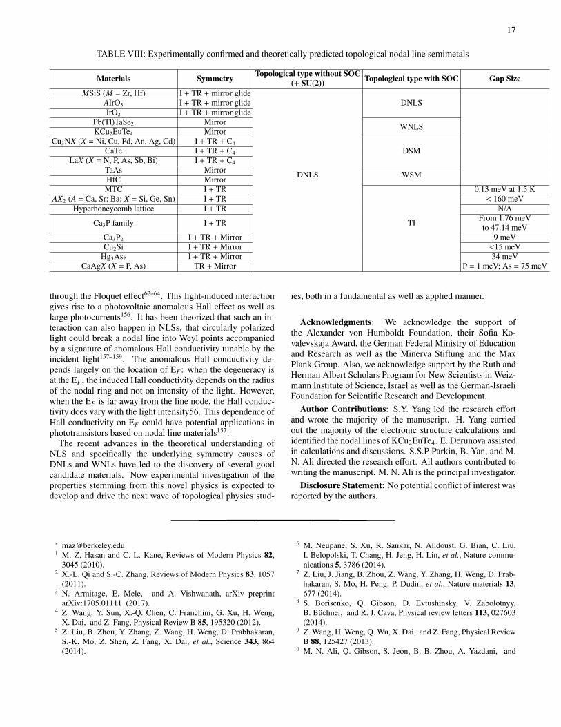
flection symmetry can protect the degeneracy on the plane ofthe mirror, and non-symmorphic symmetry forces band de-generacies at high symmetry points. Mirror reflections cangenerate new crossings rather than just split four-fold cross-ings when combined with a lack of inversion and large SOC.Table V summarizes the experimentally confirmed and the-oretically predicted topological nodal line semimetals, theirtopological category without and with SOC, their gap size (ifapplicable) as well as their corresponding crystalline symme-tries.
With several materials now predicted to house the exoticelectronic structures of NLSs, future studies will focus onexperimental investigation of the properties stemming fromthose electronic structures. Firstly, there is a large opportunityto characterize the NLSs using probes other than photoemiss-sion. As topological surface states is a characteristic signatureof the nontrivial topology, direct probing of drumhead sur-face states is the next experimental step. The dispersion of thedrumhead surface states is smaller than that of typical bulk va-lence and conduction bands, making them good candidates forstudying correlation effects at surfaces155. It is proposed thatin Dirac nodal ring systems, with coexistance of inversion andtime-reversal symmetries as well as negligible SOC, and in thesmall Hubbard interaction region, surface ferromagnetism canbe obtained and characterized by the surface mode divergenceof the spin susceptibility155. Increasing the Hubbard inter-action should drive the system into a surface charge-orderedphase through a continuous quantum phase transition155. Inaddition, the bulk DNLs can also be investigated via trans-port measurements; Novel Landau level structures in nodalring semimetals are predicted as a function of the strengthand direction of applied magnetic fields60,101. Almost non-dispersive Landau levels, as a function of momentum, havebeen predicted when the magnetic field is applied in the planeof the ring. Near the center of the ring, almost flat Dirac zeromodes are expected60.
Aside from just the fundamental physics of topologicalnodal line semimetals, more applied investigations of thesematerials have also been proposed, for example, making fu-ture spintronic devices. One route to generating spin currents(necessary in spintronics) is to use the spin Hall effect (SHE),where electric current generates a transverse spin current. Theintrinsic spin Hall conductivity (SHC) can be calculated byintegrating the spin Berry curvature over the BZ. Since anti-crossings in the electronic structure induced by SOC can leadto a large Berry curvature, to maximize SHC, one needs tomaximize the number of band anti-crossings (gapped by SOC)at EF , among other parameters. A DNL consists of an infinitenumber of Dirac points along the line of degeneracy, and, un-less protected by spatial symmetries as described earlier, aregapped due to SOC. Therefore it is natural to think that gappedDNL materials have large intrinsic SHEs. It has recently beenfound the DNL in metallic rutile oxides IrO2, OsO2, and RuO2contribute to the large SHC in these materials75.
The interaction of nodal line materials with light is anotheravenue for future work. It has been studied in DSMs andWSMs that circularly polarized light can couple with elec-trons and break the time-reversal symmetry of the material
17
TABLE VIII: Experimentally confirmed and theoretically predicted topological nodal line semimetals
Materials Symmetry Topological type without SOC(+ SU(2)) Topological type with SOC Gap Size
MSiS (M = Zr, Hf) I + TR + mirror glide
DNLS
DNLSAIrO3 I + TR + mirror glideIrO2 I + TR + mirror glide
Pb(Tl)TaSe2 Mirror WNLSKCu2EuTe4 MirrorCu3NX (X = Ni, Cu, Pd, An, Ag, Cd) I + TR + C4
DSMCaTe I + TR + C4
LaX (X = N, P, As, Sb, Bi) I + TR + C4
TaAs Mirror WSMHfC MirrorMTC I + TR
TI
0.13 meV at 1.5 KAX2 (A = Ca, Sr; Ba; X = Si, Ge, Sn) I + TR < 160 meV
Hyperhoneycomb lattice I + TR N/A
Ca3P family I + TRFrom 1.76 meVto 47.14 meV
Ca3P2 I + TR + Mirror 9 meVCu2Si I + TR + Mirror <15 meV
Hg3As2 I + TR + Mirror 34 meVCaAgX (X = P, As) TR + Mirror P = 1 meV; As = 75 meV
through the Floquet effect62–64. This light-induced interactiongives rise to a photovoltaic anomalous Hall effect as well aslarge photocurrents156. It has been theorized that such an in-teraction can also happen in NLSs, that circularly polarizedlight could break a nodal line into Weyl points accompaniedby a signature of anomalous Hall conductivity tunable by theincident light157–159. The anomalous Hall conductivity de-pends largely on the location of EF : when the degeneracy isat the EF , the induced Hall conductivity depends on the radiusof the nodal ring and not on intensity of the light. However,when the EF is far away from the line node, the Hall conduc-tivity does vary with the light intensity56. This dependence ofHall conductivity on EF could have potential applications inphototransistors based on nodal line materials157.
The recent advances in the theoretical understanding ofNLS and specifically the underlying symmetry causes ofDNLs and WNLs have led to the discovery of several goodcandidate materials. Now experimental investigation of theproperties stemming from this novel physics is expected todevelop and drive the next wave of topological physics stud-
ies, both in a fundamental as well as applied manner.
Acknowledgments: We acknowledge the support ofthe Alexander von Humboldt Foundation, their Sofia Ko-valevskaja Award, the German Federal Ministry of Educationand Research as well as the Minerva Stiftung and the MaxPlank Group. Also, we acknowledge support by the Ruth andHerman Albert Scholars Program for New Scientists in Weiz-mann Institute of Science, Israel as well as the German-IsraeliFoundation for Scientific Research and Development.
Author Contributions: S.Y. Yang led the research effortand wrote the majority of the manuscript. H. Yang carriedout the majority of the electronic structure calculations andidentified the nodal lines of KCu2EuTe4. E. Derunova assistedin calculations and discussions. S.S.P Parkin, B. Yan, and M.N. Ali directed the research effort. All authors contributed towriting the manuscript. M. N. Ali is the principal investigator.
Disclosure Statement: No potential conflict of interest wasreported by the authors.
∗ [email protected] M. Z. Hasan and C. L. Kane, Reviews of Modern Physics 82,
3045 (2010).2 X.-L. Qi and S.-C. Zhang, Reviews of Modern Physics 83, 1057
(2011).3 N. Armitage, E. Mele, and A. Vishwanath, arXiv preprint
arXiv:1705.01111 (2017).4 Z. Wang, Y. Sun, X.-Q. Chen, C. Franchini, G. Xu, H. Weng,
X. Dai, and Z. Fang, Physical Review B 85, 195320 (2012).5 Z. Liu, B. Zhou, Y. Zhang, Z. Wang, H. Weng, D. Prabhakaran,
S.-K. Mo, Z. Shen, Z. Fang, X. Dai, et al., Science 343, 864(2014).
6 M. Neupane, S. Xu, R. Sankar, N. Alidoust, G. Bian, C. Liu,I. Belopolski, T. Chang, H. Jeng, H. Lin, et al., Nature commu-nications 5, 3786 (2014).
7 Z. Liu, J. Jiang, B. Zhou, Z. Wang, Y. Zhang, H. Weng, D. Prab-hakaran, S. Mo, H. Peng, P. Dudin, et al., Nature materials 13,677 (2014).
8 S. Borisenko, Q. Gibson, D. Evtushinsky, V. Zabolotnyy,B. Buchner, and R. J. Cava, Physical review letters 113, 027603(2014).
9 Z. Wang, H. Weng, Q. Wu, X. Dai, and Z. Fang, Physical ReviewB 88, 125427 (2013).
10 M. N. Ali, Q. Gibson, S. Jeon, B. B. Zhou, A. Yazdani, and
18
R. Cava, Inorganic chemistry 53, 4062 (2014).11 S. Jeon, B. B. Zhou, A. Gyenis, B. E. Feldman, I. Kimchi, A. C.
Potter, Q. D. Gibson, R. J. Cava, A. Vishwanath, and A. Yazdani,Nature materials 13, 851 (2014).
12 J. Feng, Y. Pang, D. Wu, Z. Wang, H. Weng, J. Li, X. Dai,Z. Fang, Y. Shi, and L. Lu, Physical Review B 92, 081306(2015).
13 T. Liang, Q. Gibson, M. N. Ali, M. Liu, R. Cava, and N. Ong,Nature materials 14, 280 (2015).
14 L.-X. Wang, C.-Z. Li, D.-P. Yu, and Z.-M. Liao, Nature commu-nications 7 (2016).
15 H. B. Nielsen and M. Ninomiya, Nuclear Physics B 185, 20(1981).
16 H. B. Nielsen and M. Ninomiya, Nuclear Physics B 193, 173(1981).
17 Z. Fang, N. Nagaosa, K. S. Takahashi, A. Asamitsu, R. Math-ieu, T. Ogasawara, H. Yamada, M. Kawasaki, Y. Tokura, andK. Terakura, Science 302, 92 (2003).
18 X. Wan, A. M. Turner, A. Vishwanath, and S. Y. Savrasov, Phys-ical Review B 83, 205101 (2011).
19 L. Balents, Physics 4, 36 (2011).20 G. Xu, H. Weng, Z. Wang, X. Dai, and Z. Fang, Physical review
letters 107, 186806 (2011).21 H. Weng, C. Fang, Z. Fang, B. A. Bernevig, and X. Dai, Physical
Review X 5, 011029 (2015).22 S.-M. Huang, S.-Y. Xu, I. Belopolski, C.-C. Lee, G. Chang,
B. Wang, N. Alidoust, G. Bian, M. Neupane, C. Zhang, et al.,Nature communications 6, 7373 (2015).
23 H. B. Nielsen and M. Ninomiya, Physics Letters B 130, 389(1983).
24 P. Hosur, S. Parameswaran, and A. Vishwanath, Physical reviewletters 108, 046602 (2012).
25 D. Son and B. Spivak, Physical Review B 88, 104412 (2013).26 H.-J. Kim, K.-S. Kim, J.-F. Wang, M. Sasaki, N. Satoh,
A. Ohnishi, M. Kitaura, M. Yang, and L. Li, Physical reviewletters 111, 246603 (2013).
27 S. Parameswaran, T. Grover, D. Abanin, D. Pesin, and A. Vish-wanath, Physical Review X 4, 031035 (2014).
28 J. Xiong, S. K. Kushwaha, T. Liang, J. W. Krizan,M. Hirschberger, W. Wang, R. Cava, and N. Ong, Science 350,413 (2015).
29 C.-Z. Li, L.-X. Wang, H. Liu, J. Wang, Z.-M. Liao, and D.-P. Yu,Nature communications 6, 10137 (2015).
30 F. Arnold, C. Shekhar, S.-C. Wu, Y. Sun, R. D. Dos Reis, N. Ku-mar, M. Naumann, M. O. Ajeesh, M. Schmidt, A. G. Grushin,et al., Nature communications 7, 11615 (2016).
31 C. Zhang, E. Zhang, W. Wang, Y. Liu, Z.-G. Chen, S. Lu,S. Liang, J. Cao, X. Yuan, L. Tang, et al., Nature communica-tions 8, 13741 (2017).
32 M. Hirschberger, S. Kushwaha, Z. Wang, Q. Gibson, S. Liang,C. Belvin, B. Bernevig, R. Cava, N. Ong, et al., Nature Materials15, 1161 (2016).
33 P. Hosur and X. Qi, Comptes Rendus Physique 14, 857 (2013).34 G. Volovik, Physica Scripta 2015, 014014 (2015).35 S.-Y. Xu, I. Belopolski, N. Alidoust, M. Neupane, G. Bian,
C. Zhang, R. Sankar, G. Chang, Z. Yuan, C.-C. Lee, et al., Sci-ence 349, 613 (2015).
36 B. Lv, H. Weng, B. Fu, X. Wang, H. Miao, J. Ma, P. Richard,X. Huang, L. Zhao, G. Chen, et al., Physical Review X 5, 031013(2015).
37 L. Yang, Z. Liu, Y. Sun, H. Peng, H. Yang, T. Zhang, B. Zhou,Y. Zhang, Y. Guo, M. Rahn, et al., Nature physics 11, 728 (2015).
38 S.-Y. Xu, N. Alidoust, I. Belopolski, Z. Yuan, G. Bian, T.-R.Chang, H. Zheng, V. N. Strocov, D. S. Sanchez, G. Chang, et al.,
Nature Physics 11, 748 (2015).39 S. Souma, Z. Wang, H. Kotaka, T. Sato, K. Nakayama, Y. Tanaka,
H. Kimizuka, T. Takahashi, K. Yamauchi, T. Oguchi, et al., Phys-ical Review B 93, 161112 (2016).
40 Z. Liu, L. Yang, Y. Sun, T. Zhang, H. Peng, H. Yang, C. Chen,Y. Zhang, Y. Guo, D. Prabhakaran, et al., Nature materials 15, 27(2016).
41 L. Lu, Z. Wang, D. Ye, L. Ran, L. Fu, J. D. Joannopoulos, andM. Soljacic, Science 349, 622 (2015).
42 A. A. Soluyanov, D. Gresch, Z. Wang, Q. Wu, M. Troyer, X. Dai,and B. A. Bernevig, Nature 527, 495 (2015).
43 Y. Sun, S.-C. Wu, M. N. Ali, C. Felser, and B. Yan, PhysicalReview B 92, 161107 (2015).
44 L. Huang, T. M. McCormick, M. Ochi, Z. Zhao, M.-T. Suzuki,R. Arita, Y. Wu, D. Mou, H. Cao, J. Yan, et al., Nature materials15, 1155 (2016).
45 K. Deng, G. Wan, P. Deng, K. Zhang, S. Ding, E. Wang, M. Yan,H. Huang, H. Zhang, Z. Xu, et al., Nature Physics 12, 1105(2016).
46 J. Jiang, Z. Liu, Y. Sun, H. Yang, C. Rajamathi, Y. Qi, L. Yang,C. Chen, H. Peng, C. Hwang, et al., Nature communications 8,13973 (2017).
47 A. Tamai, Q. Wu, I. Cucchi, F. Y. Bruno, S. Ricco, T. Kim,M. Hoesch, C. Barreteau, E. Giannini, C. Besnard, et al., Physi-cal Review X 6, 031021 (2016).
48 X. Huang, L. Zhao, Y. Long, P. Wang, D. Chen, Z. Yang,H. Liang, M. Xue, H. Weng, Z. Fang, et al., Physical ReviewX 5, 031023 (2015).
49 J. Du, H. Wang, Q. Chen, Q. Mao, R. Khan, B. Xu, Y. Zhou,Y. Zhang, J. Yang, B. Chen, et al., SCIENCE CHINA Physics,Mechanics & Astronomy 59, 1 (2016).
50 X. Yang, Y. Liu, Z. Wang, Y. Zheng, and Z.-a. Xu, arXiv preprintarXiv:1506.03190 (2015).
51 M. Ali, J. Xiong, S. Flynn, J. Tao, Q. Gibson, L. Schoop,T. Liang, N. Haldolaarachchige, M. Hirschberger, N. Ong, et al.,Nature 514, 205 (2014).
52 C. Shekhar, A. K. Nayak, Y. Sun, M. Schmidt, M. Nicklas,I. Leermakers, U. Zeitler, Y. Skourski, J. Wosnitza, Z. Liu, et al.,Nature Physics 11, 645 (2015).
53 T. Bzdusek, Q. Wu, A. Ruegg, M. Sigrist, A. Soluyanov, et al.,Nature 538, 75 (2016).
54 H. Weng, Y. Liang, Q. Xu, R. Yu, Z. Fang, X. Dai, and Y. Kawa-zoe, Physical Review B 92, 045108 (2015).
55 A. Burkov, M. Hook, and L. Balents, Physical Review B 84,235126 (2011).
56 T. T. Heikkila and G. E. Volovik, JETP letters 93, 59 (2011).57 N. Kopnin, T. Heikkila, and G. Volovik, Physical Review B 83,
220503 (2011).58 T. T. Heikkila, N. B. Kopnin, and G. E. Volovik, JETP letters 94,
233 (2011).59 Y. Huh, E.-G. Moon, and Y. B. Kim, Physical Review B 93,
035138 (2016).60 J.-W. Rhim and Y. B. Kim, Physical Review B 92, 045126
(2015).61 S. T. Ramamurthy and T. L. Hughes, arXiv preprint
arXiv:1508.01205 (2015).62 S. Ebihara, K. Fukushima, and T. Oka, Physical Review B 93,
155107 (2016).63 C.-K. Chan, P. A. Lee, K. S. Burch, J. H. Han, and Y. Ran,
Physical review letters 116, 026805 (2016).64 K. Taguchi, T. Imaeda, M. Sato, and Y. Tanaka, Physical Review
B 93, 201202 (2016).65 R. Takahashi, M. Hirayama, and S. Murakami, arXiv preprint
arXiv:1704.02151 (2017).
19
66 C. Fang, Y. Chen, H.-Y. Kee, and L. Fu, Physical Review B 92,081201 (2015).
67 C. Fang, H. Weng, X. Dai, and Z. Fang, Chinese Physics B 25,117106 (2016).
68 B. Yan and C. Felser, Annual Review of Condensed MatterPhysics 8, 337 (2017).
69 S. Jia, S.-Y. Xu, and M. Z. Hasan, Nature materials 15, 1140(2016).
70 S. Wang, B.-C. Lin, A.-Q. Wang, D.-P. Yu, and Z.-M. Liao, Ad-vances in Physics: X 2, 518 (2017).
71 R. Yu, Z. Fang, X. Dai, and H. Weng, Frontiers of Physics 12,127202 (2017).
72 H. Weng, X. Dai, and Z. Fang, J. Phys.: Condens. Matter 28,303001 (2016).
73 G. Bian, T.-R. Chang, R. Sankar, S.-Y. Xu, H. Zheng, T. Neupert,C.-K. Chiu, S.-M. Huang, G. Chang, I. Belopolski, et al., Naturecommunications 7, 10556 (2016).
74 L. M. Schoop, M. N. Ali, C. Straßer, A. Topp, A. Varykhalov,D. Marchenko, V. Duppel, S. S. Parkin, B. V. Lotsch, and C. R.Ast, Nature communications 7, 11696 (2016).
75 Y. Sun, Y. Zhang, C.-X. Liu, C. Felser, and B. Yan, arXivpreprint arXiv:1701.09089 (2017).
76 Z. Liu, M. Li, Q. Li, J. Liu, W. Li, H. Yang, Q. Yao, C. Fan,X. Wan, Z. Wang, et al., Scientific reports 6, 30309 (2016).
77 M. Neupane, I. Belopolski, M. M. Hosen, D. S. Sanchez,R. Sankar, M. Szlawska, S.-Y. Xu, K. Dimitri, N. Dhakal, P. Mal-donado, et al., Physical Review B 93, 201104 (2016).
78 C. Chen, X. Xu, J. Jiang, S.-C. Wu, Y. Qi, L. Yang, M. Wang,Y. Sun, N. Schroter, H. Yang, et al., Physical Review B 95,125126 (2017).
79 M. N. Ali, Q. D. Gibson, T. Klimczuk, and R. Cava, PhysicalReview B 89, 020505 (2014).
80 S.-Y. Guan, P.-J. Chen, M.-W. Chu, R. Sankar, F. Chou, H.-T.Jeng, C.-S. Chang, and T.-M. Chuang, Science Advances 2,e1600894 (2016).
81 T.-R. Chang, P.-J. Chen, G. Bian, S.-M. Huang, H. Zheng, T. Ne-upert, R. Sankar, S.-Y. Xu, I. Belopolski, G. Chang, et al., Phys-ical Review B 93, 245130 (2016).
82 G. Bian, T.-R. Chang, H. Zheng, S. Velury, S.-Y. Xu, T. Neupert,C.-K. Chiu, S.-M. Huang, D. S. Sanchez, I. Belopolski, et al.,Physical Review B 93, 121113 (2016).
83 Y. Kim, B. J. Wieder, C. Kane, and A. M. Rappe, Physical reviewletters 115, 036806 (2015).
84 R. Yu, H. Weng, Z. Fang, X. Dai, and X. Hu, Physical reviewletters 115, 036807 (2015).
85 R. Yu, Q. Wu, Z. Fang, and H. Weng, arXiv preprintarXiv:1701.08502 (2017).
86 Q. Gibson, L. Schoop, L. Muechler, L. Xie, M. Hirschberger,N. Ong, R. Car, and R. Cava, Physical Review B 91, 205128(2015).
87 S. M. Young and C. L. Kane, Physical review letters 115, 126803(2015).
88 S. Murakami, 139 (2017).89 Y.-H. Chan, C.-K. Chiu, M. Chou, and A. P. Schnyder, Physical
Review B 93, 205132 (2016).90 R. Hoffmann, Angewandte Chemie International Edition in En-
glish 26, 846 (1987).91 W. Tremel and R. Hoffmann, J. Am. Chem. Soc 109, 124 (1987).92 Y. Du, F. Tang, D. Wang, L. Sheng, E.-j. Kan, C.-G. Duan, S. Y.
Savrasov, and X. Wan, arXiv preprint arXiv:1605.07998 (2016).93 M. Zeng, C. Fang, G. Chang, Y.-A. Chen, T. Hsieh, A. Bansil,
H. Lin, and L. Fu, arXiv preprint arXiv:1504.03492 (2015).94 L. S. Xie, L. M. Schoop, E. M. Seibel, Q. D. Gibson, W. Xie,
and R. J. Cava, Apl Materials 3, 083602 (2015).
95 Q. Xu, R. Yu, Z. Fang, X. Dai, and H. Weng, Physical Review B95, 045136 (2017).
96 H. Huang, J. Liu, D. Vanderbilt, and W. Duan, Physical ReviewB 93, 201114 (2016).
97 J. Nayak, S.-C. Wu, N. Kumar, C. Shekhar, S. Singh, J. Fink,E. E. Rienks, G. H. Fecher, S. S. Parkin, B. Yan, et al., Naturecommunications 8 (2017).
98 X. Feng, C. Yue, Z. Song, Q. Wu, and B. Wen, arXiv preprintarXiv:1705.00511 (2017).
99 R. Kumar, M. Mishra, B. Sharma, V. Sharma, J. Lowther,V. Vyas, and G. Sharma, Computational Materials Science 61,150 (2012).
100 X. Zhang, Z.-M. Yu, X.-L. Sheng, H. Y. Yang, and S. A. Yang,Physical Review B 95, 235116 (2017).
101 K. Mullen, B. Uchoa, and D. T. Glatzhofer, Physical review let-ters 115, 026403 (2015).
102 B. Feng, B. Fu, S. Kasamatsu, S. Ito, P. Cheng, C.-C. Liu, S. K.Mahatha, P. Sheverdyaeva, P. Moras, M. Arita, et al., arXivpreprint arXiv:1611.09578 (2016).
103 J. Lu, W. Luo, X. Li, S. Yang, J. Cao, X. Gong, and H. Xiang,arXiv preprint arXiv:1603.04596 (2016).
104 F. F. Tafti, Q. Gibson, S. Kushwaha, J. W. Krizan, N. Hal-dolaarachchige, and R. J. Cava, Proceedings of the NationalAcademy of Sciences 113, E3475 (2016).
105 F. Tafti, Q. Gibson, S. Kushwaha, N. Haldolaarachchige, andR. Cava, Nature Physics 12, 272 (2016).
106 N. Kumar, C. Shekhar, S.-C. Wu, I. Leermakers, O. Young,U. Zeitler, B. Yan, and C. Felser, Physical Review B 93, 241106(2016).
107 L.-K. Zeng, R. Lou, D.-S. Wu, Q. Xu, P.-J. Guo, L.-Y. Kong, Y.-G. Zhong, J.-Z. Ma, B.-B. Fu, P. Richard, et al., Physical reviewletters 117, 127204 (2016).
108 Y. Wu, T. Kong, L.-L. Wang, D. D. Johnson, D. Mou, L. Huang,B. Schrunk, S. L. Bud’ko, P. C. Canfield, and A. Kaminski, Phys-ical Review B 94, 081108 (2016).
109 A. Waskowska, L. Gerward, J. S. Olsen, K. R. Babu,G. Vaitheeswaran, V. Kanchana, A. Svane, V. Filipov,G. Levchenko, and A. Lyaschenko, Acta Materialia 59, 4886(2011).
110 N. L. Okamoto, M. Kusakari, K. Tanaka, H. Inui, and S. Otani,Acta Materialia 58, 76 (2010).
111 M. Ezawa, Physical review letters 116, 127202 (2016).112 E. K.-H. Lee, S. Bhattacharjee, K. Hwang, H.-S. Kim, H. Jin,
and Y. B. Kim, Physical Review B 89, 205132 (2014).113 T. Takayama, A. Kato, R. Dinnebier, J. Nuss, H. Kono, L. Veiga,
G. Fabbris, D. Haskel, and H. Takagi, Physical review letters114, 077202 (2015).
114 A. Biffin, R. Johnson, S. Choi, F. Freund, S. Manni, A. Bombardi,P. Manuel, P. Gegenwart, and R. Coldea, Physical Review B 90,205116 (2014).
115 K. A. Modic, T. E. Smidt, I. Kimchi, N. P. Breznay, A. Biffin,S. Choi, R. D. Johnson, R. Coldea, P. Watkins-Curry, G. T. Mc-Candless, et al., arXiv preprint arXiv:1402.3254 (2014).
116 E. K.-H. Lee, R. Schaffer, S. Bhattacharjee, and Y. B. Kim, Phys-ical Review B 89, 045117 (2014).
117 I. Kimchi, J. G. Analytis, and A. Vishwanath, Physical ReviewB 90, 205126 (2014).
118 S. Lee, E. K.-H. Lee, A. Paramekanti, and Y. B. Kim, PhysicalReview B 89, 014424 (2014).
119 G. Pang, M. Smidman, L. Zhao, Y. Wang, Z. Weng, L. Che,Y. Chen, X. Lu, G. Chen, and H. Yuan, Physical Review B 93,060506 (2016).
120 C.-L. Zhang, Z. Yuan, G. Bian, S.-Y. Xu, X. Zhang, M. Z. Hasan,and S. Jia, Physical Review B 93, 054520 (2016).
20
121 R. Sankar, G. N. Rao, I. P. Muthuselvam, T.-R. Chang, H. Jeng,G. S. Murugan, W.-L. Lee, and F. Chou, Journal of Physics:Condensed Matter 29, 095601 (2017).
122 I. Belopolski, S.-Y. Xu, D. S. Sanchez, G. Chang, C. Guo, M. Ne-upane, H. Zheng, C.-C. Lee, S.-M. Huang, G. Bian, et al., Phys-ical review letters 116, 066802 (2016).
123 H. Inoue, A. Gyenis, Z. Wang, J. Li, S. W. Oh, S. Jiang, N. Ni,B. A. Bernevig, and A. Yazdani, Science 351, 1184 (2016).
124 R. Batabyal, N. Morali, N. Avraham, Y. Sun, M. Schmidt,C. Felser, A. Stern, B. Yan, and H. Beidenkopf, Science ad-vances 2, e1600709 (2016).
125 N. J. Ghimire, Y. Luo, M. Neupane, D. Williams, E. Bauer, andF. Ronning, Journal of Physics: Condensed Matter 27, 152201(2015).
126 Z. Wang, Y. Zheng, Z. Shen, Y. Lu, H. Fang, F. Sheng, Y. Zhou,X. Yang, Y. Li, C. Feng, et al., Physical Review B 93, 121112(2016).
127 C.-L. Zhang, S.-Y. Xu, I. Belopolski, Z. Yuan, Z. Lin, B. Tong,G. Bian, N. Alidoust, C.-C. Lee, S.-M. Huang, et al., Nature com-munications 7 (2016).
128 Y. Luo, N. Ghimire, M. Wartenbe, H. Choi, M. Neupane, R. Mc-Donald, E. Bauer, J. Zhu, J. Thompson, and F. Ronning, PhysicalReview B 92, 205134 (2015).
129 P. J. Moll, A. C. Potter, N. L. Nair, B. Ramshaw, K. Modic,S. Riggs, B. Zeng, N. J. Ghimire, E. D. Bauer, R. Kealhofer,et al., Nature communications 7 (2016).
130 A. Yamakage, Y. Yamakawa, Y. Tanaka, and Y. Okamoto, Jour-nal of the Physical Society of Japan 85, 013708 (2015).
131 D. Takane, Z. Wang, S. Souma, K. Nakayama, C. Trang, T. Sato,T. Takahashi, and Y. Ando, Physical Review B 94, 121108(2016).
132 M. N. Ali, L. M. Schoop, C. Garg, J. M. Lippmann, E. Lara,B. Lotsch, and S. Parkin, arXiv preprint arXiv:1603.09318(2016).
133 X. Wang, X. Pan, M. Gao, J. Yu, J. Jiang, J. Zhang,H. Zuo, M. Zhang, Z. Wei, W. Niu, et al., arXiv preprintarXiv:1604.00108 (2016).
134 R. Singha, A. Pariari, B. Satpati, and P. Mandal, arXiv preprintarXiv:1602.01993 (2016).
135 J. Hu, Z. Tang, J. Liu, Y. Zhu, J. Wei, and Z. Mao, arXiv preprintarXiv:1604.01567 (2016).
136 N. Kumar, K. Manna, Y. Qi, S.-C. Wu, L. Wang, B. Yan,C. Felser, and C. Shekhar, arXiv preprint arXiv:1612.05176(2016).
137 A. Topp, J. M. Lippmann, A. Varykhalov, V. Duppel, B. V.Lotsch, C. R. Ast, and L. M. Schoop, New Journal of Physics18, 125014 (2016).
138 Y.-Y. Lv, B.-B. Zhang, X. Li, S.-H. Yao, Y. Chen, J. Zhou, S.-T.Zhang, M.-H. Lu, and Y.-F. Chen, Applied Physics Letters 108,244101 (2016).
139 Y. Nie, P. King, C. Kim, M. Uchida, H. Wei, B. Faeth, J. Ruf,J. Ruff, L. Xie, X. Pan, et al., Physical review letters 114, 016401(2015).
140 R. Lou, J.-Z. Ma, Q.-N. Xu, B.-B. Fu, L.-Y. Kong, Y.-G. Shi,P. Richard, H.-M. Weng, Z. Fang, S.-S. Sun, et al., Physical Re-view B 93, 241104 (2016).
141 J. Hu, Z. Tang, J. Liu, X. Liu, Y. Zhu, D. Graf, K. Myhro, S. Tran,C. N. Lau, J. Wei, et al., Physical Review Letters 117, 016602(2016).
142 Q. Xu, Z. Song, S. Nie, H. Weng, Z. Fang, and X. Dai, PhysicalReview B 92, 205310 (2015).
143 Y. Chen, Y.-M. Lu, and H.-Y. Kee, Nature communications 6,6593 (2015).
144 M. A. Zeb and H.-Y. Kee, Physical Review B 86, 085149 (2012).145 J.-M. Carter, V. V. Shankar, M. A. Zeb, and H.-Y. Kee, Physical
Review B 85, 115105 (2012).146 J. Liu, D. Kriegner, L. Horak, D. Puggioni, C. R. Serrao, R. Chen,
D. Yi, C. Frontera, V. Holy, A. Vishwanath, et al., Physical Re-view B 93, 085118 (2016).
147 J. Fujioka, T. Okawa, A. Yamamoto, and Y. Tokura, PhysicalReview B 95, 121102 (2017).
148 L. Zhang, Y. Chen, B. Zhang, J. Zhou, S. Zhang, Z. Gu, S. Yao,and Y. Chen, Journal of the Physical Society of Japan 83, 054707(2014).
149 J. H. Gruenewald, J. Nichols, J. Terzic, G. Cao, J. W. Brill, andS. S. A. Seo, Journal of Materials Research 29, 2491 (2014).
150 A. Biswas, K.-S. Kim, and Y. H. Jeong, Journal of AppliedPhysics 116, 213704 (2014).
151 A. P. Schnyder, S. Ryu, A. Furusaki, and A. W. Ludwig, PhysicalReview B 78, 195125 (2008).
152 J. Lin, S. Huang, Y. Lin, T. Lee, H. Liu, X. Zhang, R. Chen,and Y. Huang, Journal of Physics: Condensed Matter 16, 8035(2004).
153 W. Ryden, W. Reed, and E. Greiner, Physical Review B 6, 2089(1972).
154 R. Patschke, P. Brazis, C. R. Kannewurf, and M. G. Kanatzidis,Journal of Materials Chemistry 9, 2293 (1999).
155 J. Liu and L. Balents, Physical Review B 95, 075426 (2017).156 C.-K. Chan, N. H. Lindner, G. Refael, and P. A. Lee, Physical
Review B 95, 041104 (2017).157 K. Taguchi, D.-H. Xu, A. Yamakage, and K. Law, Physical Re-
view B 94, 155206 (2016).158 Z. Yan and Z. Wang, Physical review letters 117, 087402 (2016).159 M. Ezawa, arXiv preprint arXiv:1705.02140 (2017)
.