synthesis of thin films - masaryk university · 2006-11-19 · thin films 19 synthesis of thin...
TRANSCRIPT

Thin Films 1
SYNTHESIS OF THIN FILMS
THIN FILMS ARE VITAL IN MODERN TECHNOLOGY:
Protective coatingsOptical coatingsFilters, mirrors, lensesMicroelectronic devicesOptoelectronic devicesPhotonic devicesElectrode surfacesPhotoelectric devices, photovoltaics, solar cellsXerographyPhotographyLithographyCatalyst surfacesInformation storage, magnetic, magneto-optical, optical memories
Thin Films 2
SYNTHESIS OF THIN FILMS
Crystalline, Amorphous, Microcrystalline
Monolayer, multilayer, superlattice, junctions
Free-standing, supported
Epitaxial (commensurate), incommensurate
Thin Films 3
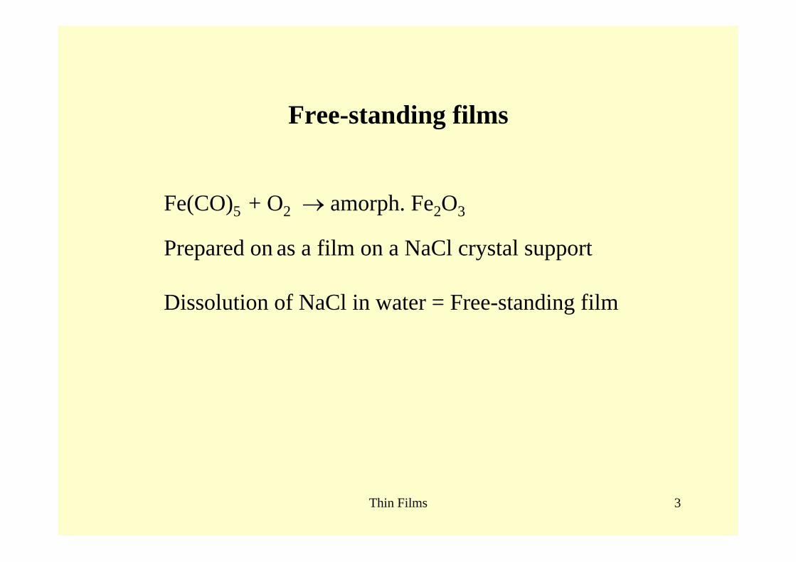
Free-standing films
Fe(CO)5 + O2 → amorph. Fe2O3
Prepared on as a film on a NaCl crystal support
Dissolution of NaCl in water = Free-standing film

Thin Films 4
SYNTHESIS OF THIN FILMS
FILM PROPERTIES DEPEND ON NUMEROUSCONSIDERATIONS:
ThicknessSurface : volume ratioStructure, surface versus bulk, surface reconstruction, surfaceroughnessHydrophobicity, hydrophilicy (Si-OH vs. Si-H)CompositionTexture: single crystal, microcrystalline, domains, orientationForm: supported or unsupported, nature of substrate
Thin Films 5
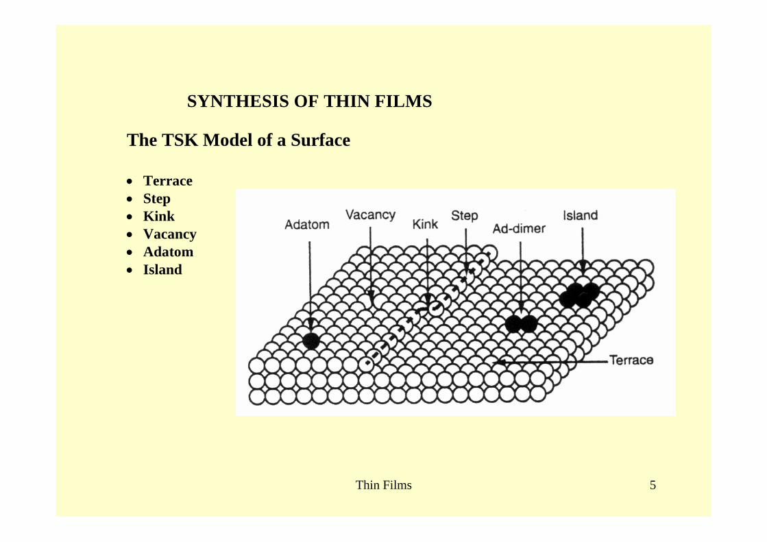
SYNTHESIS OF THIN FILMS
The TSK Model of a Surface • Terrace • Step • Kink • Vacancy • Adatom • Island

Thin Films 6

Thin Films 7
SYNTHESIS OF THIN FILMS
Surface diffusion coefficient D
D = a2 ks a … effective hopping distance between sites
ks … site-to-site hopping rate of an adatom
ks = A exp(-Vs/kbT) Vs … potential-energy barrier to hopping fromsite to site
T … substrate temperature
Higher temperature = Faster diffusion

Thin Films 8
Si(111) Surface
Silicon "diamond lattice" structure
a = 5.463 Å
Si(111) = a set of atomic planes
One plane outlined with red

Thin Films 9
Si(111) SurfaceA top view of the atomicarrangement for the (111) plane
orange = the top layergreen = deeper layers

Thin Films 10

Thin Films 11
7x7 reconstructionWhen (111) surface of Si is heated to high temperatures under the Ultra-HighVacuum conditions the surface atoms rearrange to a more energetically stableconfiguration called 7x7 reconstruction.
STM image ofSi(111) surface

Thin Films 12
7x7 reconstruction

Thin Films 13
7x7 reconstruction3D representation of the 7x7 STM imageThe image area is 18x8 nm2, the height of the "bumps" is only about 0.04 nm
Thin Films 14
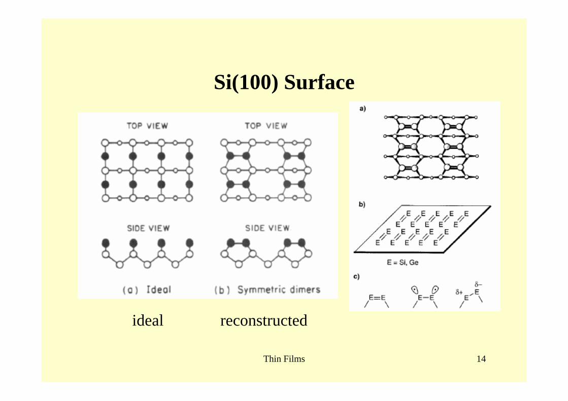
Si(100) Surface
ideal reconstructed
Thin Films 15
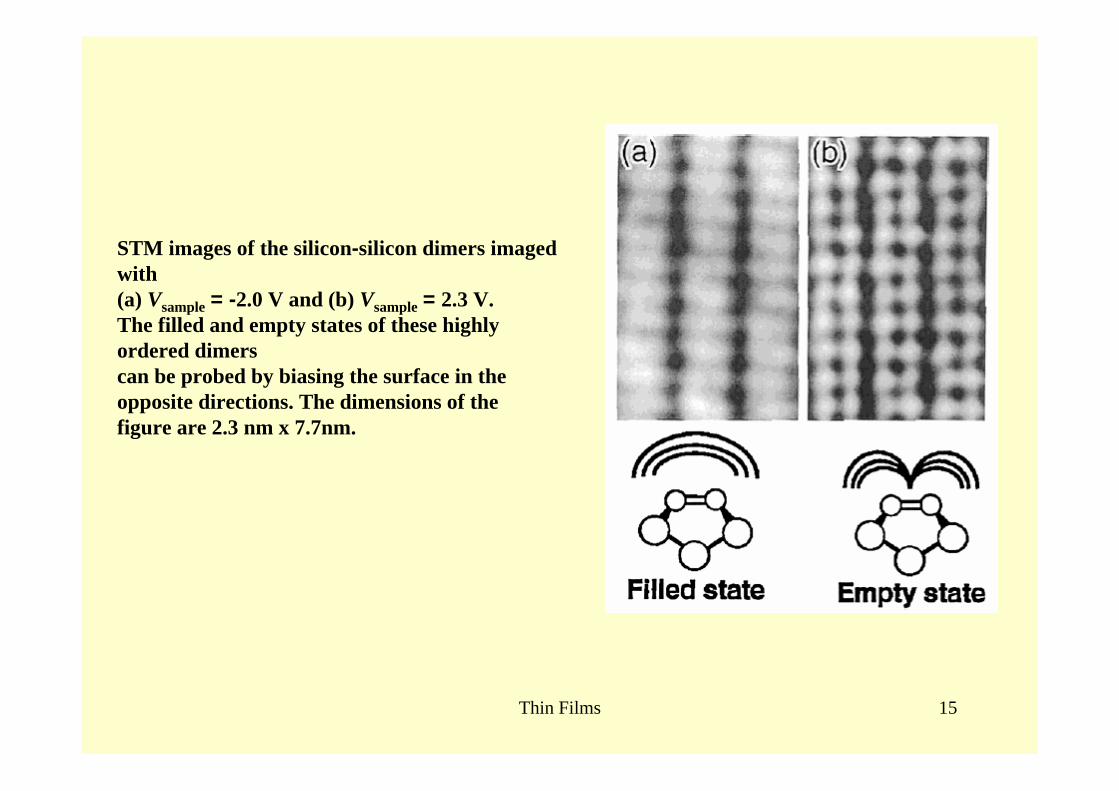
STM images of the silicon-silicon dimers imagedwith(a) Vsample = -2.0 V and (b) Vsample = 2.3 V.The filled and empty states of these highlyordered dimerscan be probed by biasing the surface in theopposite directions. The dimensions of thefigure are 2.3 nm x 7.7nm.

Thin Films 16
H-terminated Si(100) Surface

Thin Films 17
SYNTHESIS OF THIN FILMS
MAIN METHODS OF SYNTHESIZING THIN FILMS:
CHEMICAL, ELECTROCHEMICAL, PHYSICAL
Cathodic deposition, Anodic deposition, Electroless depositionThermal oxidation, nitridationChemical vapor deposition (CVD)Metal organic chemical vapor deposition (MOCVD)Molecular beam epitaxy, supersonic cluster beams, aerosoldepositionLiquid phase epitaxySelf-assembly, surface anchoring, SAMDischarge techniques, RF, microwaveLaser ablationCathode sputtering, vacuum evaporation

Thin Films 18
SYNTHESIS OF THIN FILMS
CATHODIC DEPOSITION
Two electrodes, dipped into electrolyte solutionExternal potential appliedMetal deposition onto the cathode as thin filmAnode metal slowly dissolves
ELECTROLESS DEPOSITION
Spontaneous, No applied potentialDepends on electrochemical potential difference between electrodeand solution redox active species to be deposited
Both methods limited to metallic films on conducting substrates
ANODIC DEPOSITION
Deposition of oxide films, such as alumina, titaniaDeposition of conducting polymer films by oxidative polymerizationof monomer, such as thiophene, pyrolle, anilineOxide films formed from metallic electrode in aqueous salts or acids

Thin Films 19
SYNTHESIS OF THIN FILMSExample:Anodic oxidation of aluminum in oxalic or phosphoric acid
Pt|H3PO4, H2O|Al
Al → Al3+ + 3e- anode
PO43- +2e- → PO3
3- + O2- cathode
2Al3+ + 3O2- → γ-Al2O3 (annealing) → α-Al2O3
overall electrochemistry:
2Al + 3PO43- → Al2O3 + PO3
3-
The applied potential controls the oxide thickness and the rate atwhich it forms, oxide anions from solution have to diffuse throughan Al2O3 layer of growing thickness on the reacting Al substrate, toattain an equilibrium thickness of the alumina film

Thin Films 20
SYNTHESIS OF THIN FILMS
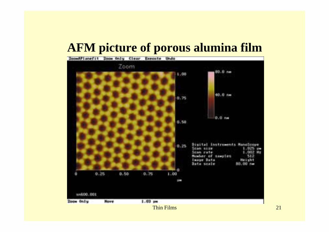
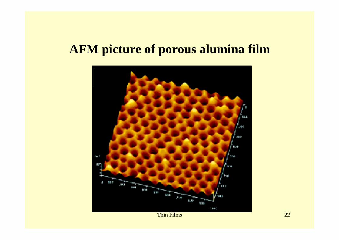
Self-organizing process observed,whereby a regular array of size tunablehcp pores form and permeateorthogonally through the alumina film
Exceptionally useful process for creating controlled porositymembranes, photonic gap materials, template for synthesizingsemiconductor nanostructures, host for synthesizing and organizingaligned carbon nanotubes for high intensity electron emissiondisplays, and last but not least, fuel cell electrode materials
Thin Films 21
AFM picture of porous alumina film
Thin Films 22
AFM picture of porous alumina film

Thin Films 23
Porous Alumina Films

Thin Films 24
SYNTHESIS OF THIN FILMS
THERMAL OXIDATION
Oxides, metal exposed to a glow discharge
Al + O2 → (RT) Al2O3, thickness 3-4 nm
Similar method applicable to other metals, Ti, V, W, Zr etc
Nitrides, exceptionally hard, high temperature protective coating
Ti + NH3 → TiN
Al + NH3 → AlN
Thin Films 25
SYNTHESIS OF THIN FILMS
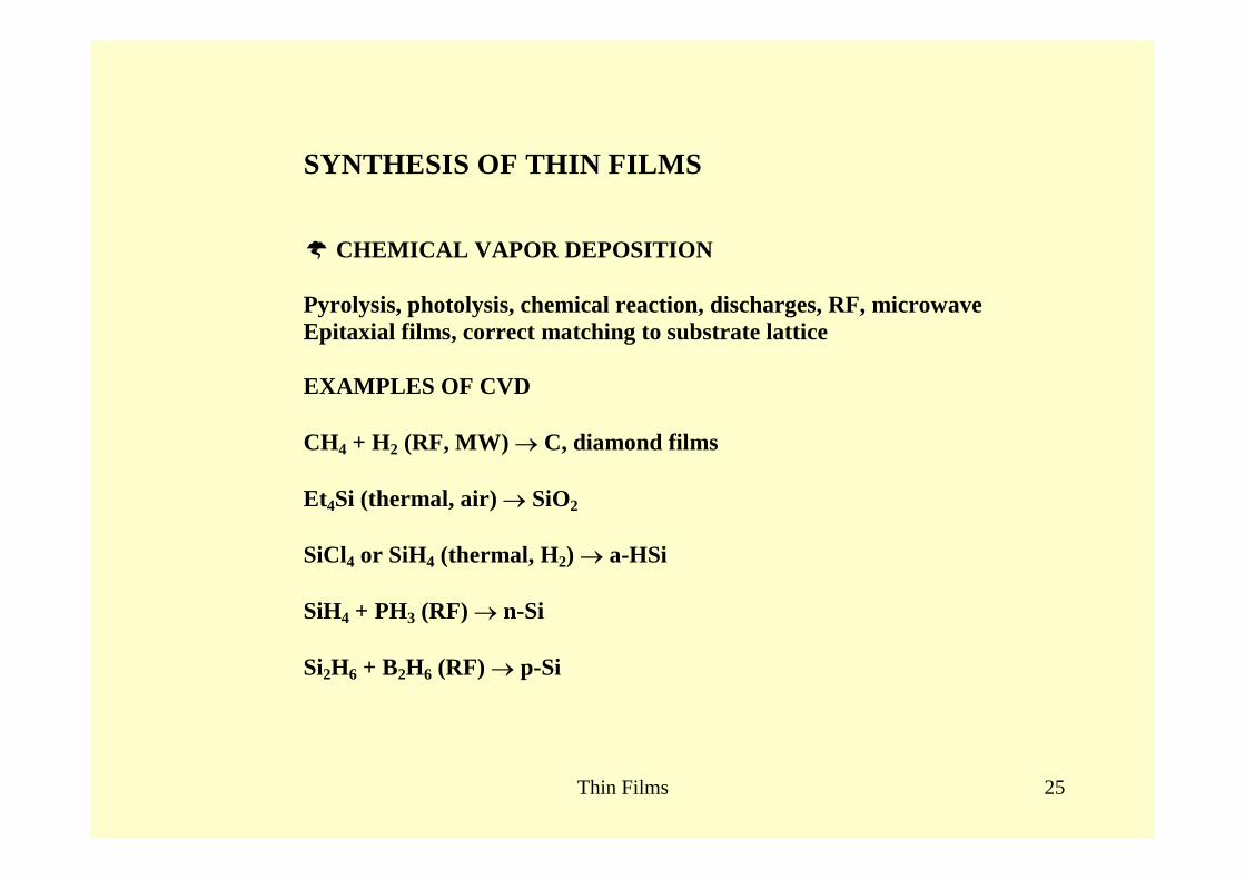
CHEMICAL VAPOR DEPOSITION
Pyrolysis, photolysis, chemical reaction, discharges, RF, microwaveEpitaxial films, correct matching to substrate lattice
EXAMPLES OF CVD
CH4 + H2 (RF, MW) → C, diamond films
Et4Si (thermal, air) → SiO2
SiCl4 or SiH4 (thermal, H2) → a-HSi
SiH4 + PH3 (RF) → n-Si
Si2H6 + B2H6 (RF) → p-Si
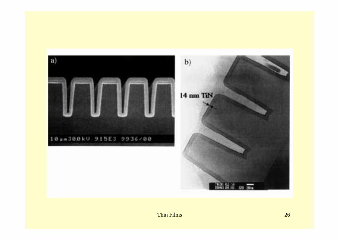
Thin Films 26

Thin Films 27
SYNTHESIS OF THIN FILMS
SiH3SiH2SiH2PH2 (RF) → n-Si
Me3Ga (laser photolysis, heating) → Ga
Me3Ga + AsH3 + H2 → GaAs + CH4
Si (laser evaporation, supersonic jet) Sin+ (size selected cluster
deposition) → Si

Thin Films 28
SYNTHESIS OF THIN FILMS
METAL ORGANIC CHEMICAL VAPOR DEPOSITION,MOCVD
Invented by Mansevit in 1968Recognized high volatility of metal organic compounds as sourcesfor semiconductor thin film preparations
MOCVD PRECURSORS, SINGLE SOURCE MATERIALS
Me3Ga, Me3Al, Et3InNH3, PH3, AsH3H2S, H2SeMe2Te, Me2Hg, Me2Zn, Me4Pb, Et2CdAll toxic materials – a problem of safe disposal of toxic waste
Example - IR detectors:Me2Cd + Me2Hg + Me2Te (H2, 500oC) → CdxHg1-xTe

Thin Films 29
SYNTHESIS OF THIN FILMS
Specially designed MOCVD reactorsControlled flow of precursors to single crystal heated substrateMost reactions occur in range 400-1300oCComplications of diffusion at interfaces, disruption of atomically flatepitaxial surfaces/interfaces occurs during depositionPhotolytic processes (photoepitaxy) help to bring the depositiontemperatures to more reasonable temperatures
REQUIREMENTS OF MOCVD PRECURSORS
RT stable, no polymerization, decompositionEasy handling, simple storageNot too reactiveVaporization without decomposition at modest T < 100oCLow rate of homogeneous pyrolysis (gas phase) wrt heterogeneousdecomposition (surface)
HOMO : HETERO rates ~ 1 : 1000
Thin Films 30
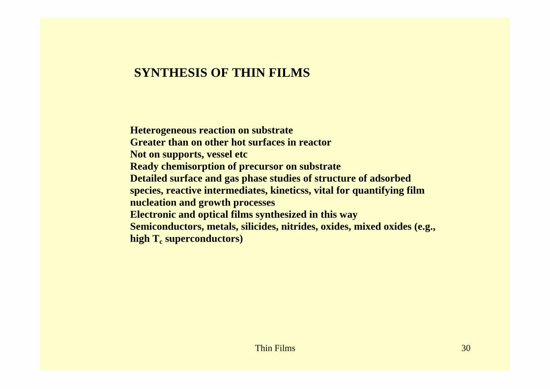
Heterogeneous reaction on substrateGreater than on other hot surfaces in reactorNot on supports, vessel etcReady chemisorption of precursor on substrateDetailed surface and gas phase studies of structure of adsorbedspecies, reactive intermediates, kineticss, vital for quantifying filmnucleation and growth processesElectronic and optical films synthesized in this waySemiconductors, metals, silicides, nitrides, oxides, mixed oxides (e.g.,high Tc superconductors)
SYNTHESIS OF THIN FILMS

Thin Films 31
CRITICAL PARAMETERS IN MATERIALS PREPARATIONFOR SYNTHESIS OF THIN FILMS
Composition controlVariety of materials to be depositedGood film uniformity over large areas to be covered, > 100 cm2
Precise reproducibilityGrowth rate, thickness control, 2-2000 nm layer thicknessPrecise control of film thickness = accurate control of deposition,film growth rateCrystal quality, epitaxyHigh degree of film perfectionDefects degrade device performancePurity of precursors: usually less than 10-9 impurity levelsStringent demands on starting material purityChallenge for chemistry, purifying and analyzing at the ppb levelDemands exceptionally clean growth system otherwise defeats theobject of controlled doping of films for device applicationsInterface widthsAbrupt changes of composition and dopant concentration required,quantum confined structures30-40 sequential layers often neededAlternating composition and graded composition films0.5-50 nm thickness required with atomic level precisionAll of the above has been more-or-less perfected in the electronicsand optics industries

Thin Films 32
SYNTHESIS OF THIN FILMS
TECHNIQUES USED TO GROW SEMICONDUCTOR FILMS ANDMULTILAYERED FILMS
MOCVD
Liquid phase epitaxy
Chemical vapor transport
Molecular beam epitaxy
Laser ablation

Thin Films 33
PHYSICAL METHODS FOR PREPARING THIN FILMS
CATHODE SPUTTERINGBell jar equipment10-1 to 10-2 torr of Ar, Kr, XeGlow discharge createdPositively charged rare gas ionsAccelerated in a high voltage to cathode targetHigh energy ions collide with cathodeSputter material from cathodeDeposits on substrate opposite cathode to form thin filmMulti-target sputtering creates composite or multilayer films
THERMAL VACUUM EVAPORATION
High vacuum bell jar > 10-6 torrHeating e-beam, resistive, laserGaseous material deposited on substrateThin films nucleate and growContainers must be chemically inert:W, Ta, Nb, Pt, BN, Al2O3, ZrO2, GraphiteSubstrates include insulators, metals, glass, alkali halides, siliconSources include metals, alloys, semiconductors, insulators, inorganicsalts

Thin Films 34
SYNTHESIS OF THIN FILMS
MOLECULAR BEAM EPITAXY
Million dollar thin film machine, ideal for preparing high qualityartificial semiconductor quantum superlattices, ferroelectrics,superconductorsUltrahigh vacuum system >10-12 torrElemental or compound sources in shutter controlled Knudseneffusion cellsAr+ ion gun for cleaning substrate surface or depth profiling sampleusing Auger analyzerHigh energy electron diffraction for surface structure analysisMass spectrometer for control and detection of vapor speciese-gun for heating the substrate
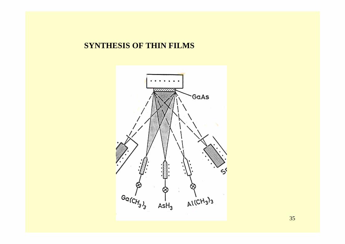
Thin Films 35
SYNTHESIS OF THIN FILMS

Thin Films 36
SYNTHESIS OF THIN FILMS
PHOTOEPITAXY
Making atomically perfect thin films under milder and morecontrolled conditions, Mullin and Tunnicliffe 1984
Et2Te + Hg (pool) + H2 (hν , 200 oC) → HgTe + 2C2H6
MOCVD preparation requires 500 oC using Me2Te + Me2Hg
Advantages of photoepitaxy
Lower temperature operationMultilayer formationLess damage of layersLower interlayer diffusionEasy to fabricate abrupt boundariesLess defects, strain, irregularities at interfaces
CdTe can be deposited onto GaAs at 200-250 oC even with a 14%lattice mismatchGaAs is susceptible to damage under MOCVD conditions 650-750 oC

Thin Films 37
SYNTHESIS OF THIN FILMS
EXTENSIONS OF PHOTOLYTIC METHODS - LASER WRITING AND LASER ETCHING
Laser writing: Substrate GaAsMe3Al or Me2Zn adsorbed layer or gas phase Focussed UV laser on film Photodissociation of organometallic precursor:
Me3Al → Al + C2H6
Creates sub-micron lines of Al or Zn

Thin Films 38
SYNTHESIS OF THIN FILMS
Laser photoetching:GaAs substrateGaseous or adsorbed layer of CH3BrFocussed UV laserCreates reactive Br atoms
CH3Br(g) (hν ) → CH3(g) + Br(g)
Br(g) + GaAs(s) → GaAs…Brn(ad)
GaAs…Brn(ad) → GaBrn(g) + AsBrn(g)
Adsorbed reactive surface Br atoms erode surface regions irradiatedwith laserVaporization of volatile gallium and arsenic bromides from surfacecreates sub-micron etched line

Thin Films 39
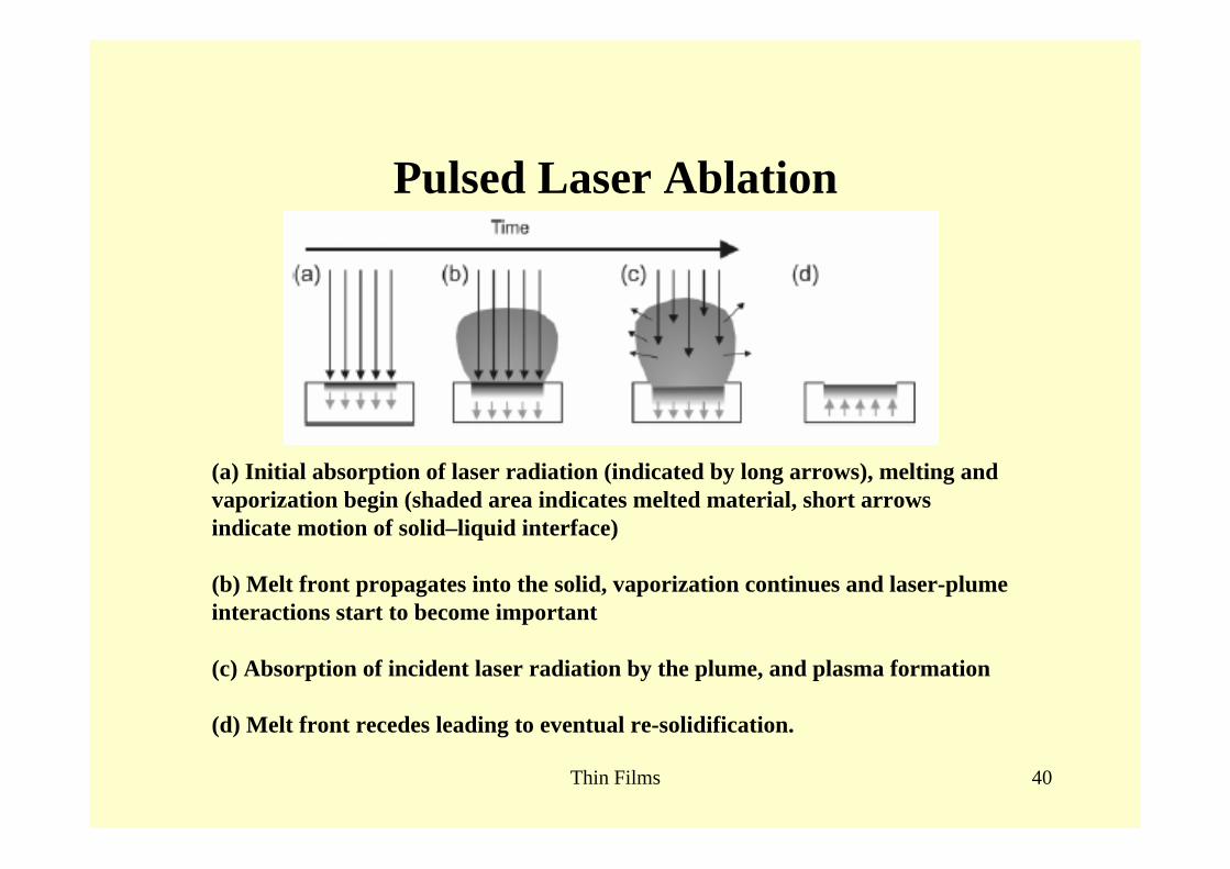
Pulsed Laser Ablation
Thin Films 40
Pulsed Laser Ablation
(a) Initial absorption of laser radiation (indicated by long arrows), melting andvaporization begin (shaded area indicates melted material, short arrowsindicate motion of solid–liquid interface)
(b) Melt front propagates into the solid, vaporization continues and laser-plumeinteractions start to become important
(c) Absorption of incident laser radiation by the plume, and plasma formation
(d) Melt front recedes leading to eventual re-solidification.

Thin Films 41
Porous Si
SEM of a porous silicon, the pores extending from the surface of the Si(100) wafer down intothe bulk, etched from n-type Si(100) (P-doped, 0.75-0.95 ø‚cm) at 77.2 mA cm-2 for 1 min with a 1:1 solution of 49% HF(aq)/ EtOH. Scale bar is 10 µm.

Thin Films 42
Porous Si
HF:EtOH = 1:2.5j = 10 mA/cm2
t = 30 min
Thin Films 43
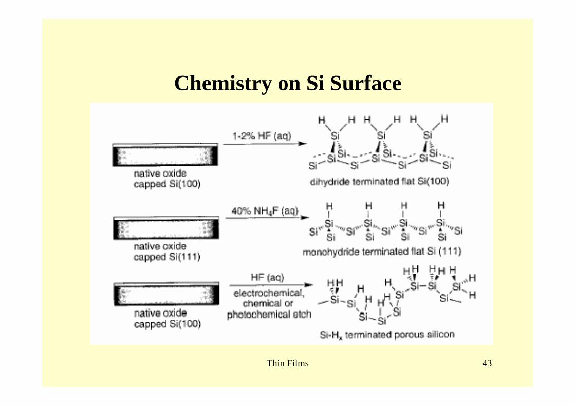
Chemistry on Si Surface

Thin Films 44
Porous Si
500 600 700 800 9000
1
2
3
4
2.4 2.2 2 1.8 1.6 1.4
PL In
tens
ity [l
in.u
.]
Wavelength [nm]
Energy [eV]
T = 295 Kλexc = 457.9 nm
Luminiscence of p-Si

Thin Films 45
Thin Films 46
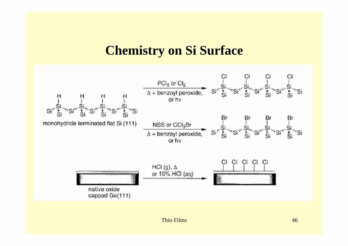
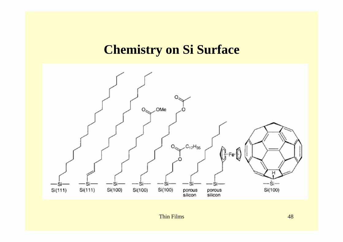
Chemistry on Si Surface

Thin Films 47
Hydrosilylation
Thin Films 48
Chemistry on Si Surface

Thin Films 49
Carbaanion LiR, RMgX

Thin Films 50

Thin Films 51
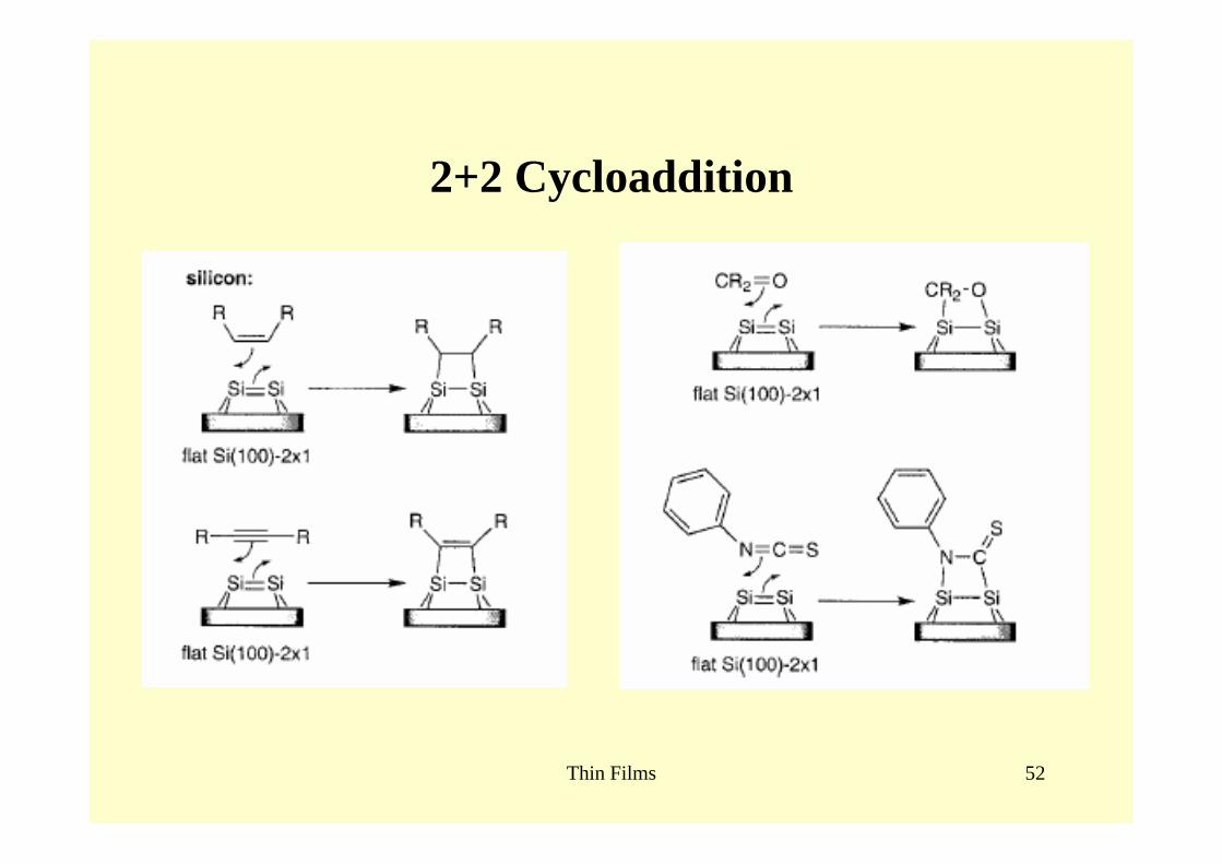
2+2 Cycloaddition
Thin Films 52
2+2 Cycloaddition
Thin Films 53
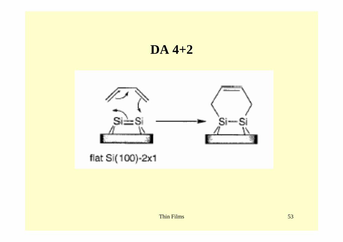
DA 4+2
Thin Films 54
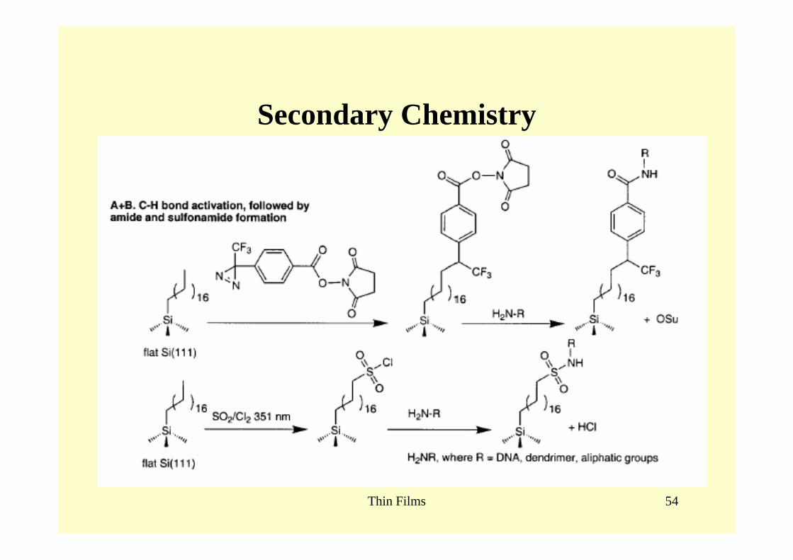
Secondary Chemistry

Thin Films 55
Secondary Chemistry

Thin Films 56
Secondary Chemistry

Thin Films 57
Secondary Chemistry
Thin Films 58
SELF-ASSEMBLED MONOLAYERS
Self-assembly: spontaneous organization of molecules into stable,structurally well-defined aggregates
Self-assembled monolayers (SAM): two-dimensional orderedassemblies of long hydrocarbon chains anchored through chemicalbonds to surfaces of solid inorganic substrates
Alkanethiolates on gold and alkylsiloxanes on silicon dioxide belongthe most notoriously studied SAM systems

Thin Films 59
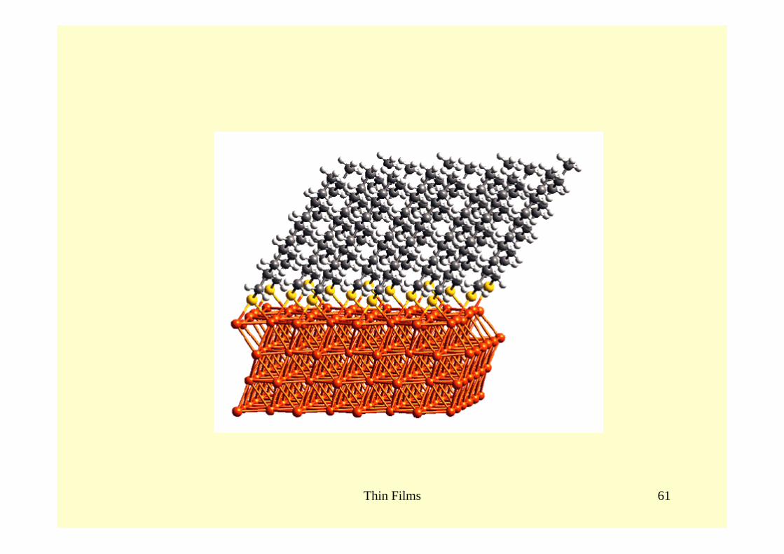
Metal surfaces Au, Ag, Cu, Pt, Hg, Fe,…react with
Thiols M + RSH M-S-R + 1/2 H2Disulfides 2 M + RSSR 2 M-S-RSulfides M + RSR M-S-R
Same products formed in all three reactions: thiolates. RSH aremore soluble and react 103 faster with Au than RSSR.
SELF-ASSEMBLED MONOLAYERS
R
S
R
S
R
S
R
S
R
S
R
S
R
S
R
S
R
S
R
S
R
S
R
S
Metal Surface
Substrates: gold polycrystalline filmson Si(SiO2), glass, mica.
Thickness 5-300 nm, sputtering, evaporation
Atomically flat

Thin Films 60
Tilt Twist
Precession
Thin Films 61

Thin Films 62

Thin Films 63
SELF-ASSEMBLED MONOLAYERS
ThermodynamicsAu does not form surface oxide layerReaction driving force:
Au-S bond energy 160-185 kJ mol-1
van der Waals attraction between alkyl chains6-8 kJ mol-1 per CH2
In tBuSH and n-C18SH competition reaction, the linear alkyl thiolbinds 300 – 700 times better.
Surface coverage 1014 molecules per cm2
C16 chain length ∼2.2 nm, 32-40° tilted, all-trans
Chemical stability: Cu/C18SH sustains HNO3Thermal stability: Au/RSH loses sulfur at 170-230 °C

Thin Films 64
SELF-ASSEMBLED MONOLAYERS
Binding modes on Au(111) On-top sites Hollow sites – threefold, more stable by 25 kJ mol-1
Bridging sites – the most stable!! (QM calculations)
Au – S – C = 180°, spAu – S – C = 104°, sp3, more stable by 1.7 kJ mol-1
barrier to interconversion 10.5 kJ mol-1

Thin Films 65
SELF-ASSEMBLED MONOLAYERS
Au(111)Hexagonal array of S, S….S distance 4.97 Å, interchain distance incrystalline paraffins 4.65 Å, tilt angles 25 - 30° to reestablish alkylchain contacts, hollow site binding, 21.4 Å2 per molecule
Ag(111)Hexagonal array of S, S….S distance 4.41 Å, on-top site binding,more tightly packed alkyl chains, no tilt

Thin Films 66
SELF-ASSEMBLED MONOLAYERS
KineticsAu(111) + RSH reactions proceed in two steps:
1. First step, fast (minutes), diffusion controlled Langmuiradsorption, concentration dependent (1 mM ∼ 1 min, 1 µM ∼ 100min)
2. Second step, slow (hours), disordered film orders to a 2D crystal,surface crystallization, defect healing, trapped solvent expulsion.Mechanisms: alkyl chain flipping, RS- lateral diffusion, equilibriumwith dissolved RSH, Au atom diffusion, Au in solution. Bettercrystallinity of films in polar solvents: MeOH, EtOH,…

Thin Films 67
SELF-ASSEMBLED MONOLAYERS
Surface chemical derivatization
HS – (CH2)n – XX = CH3, CF3, OH, NH2, SH, COOH, COOR, CN, CH=CH2, C≡CH,Cl, Br, OCH3, SO3H, SiMe3, ferrocenyl, ….
Microfabrication
♠ Self-assembly, at thermodynamic minima, rejects defects, highdegree of perfection.♠ Dimension in the range 1 nm to 1000 µm, too large for chemicalsynthesis, too small for microlithography.♠ High efficiency, spontaneous.
Thin Films 68
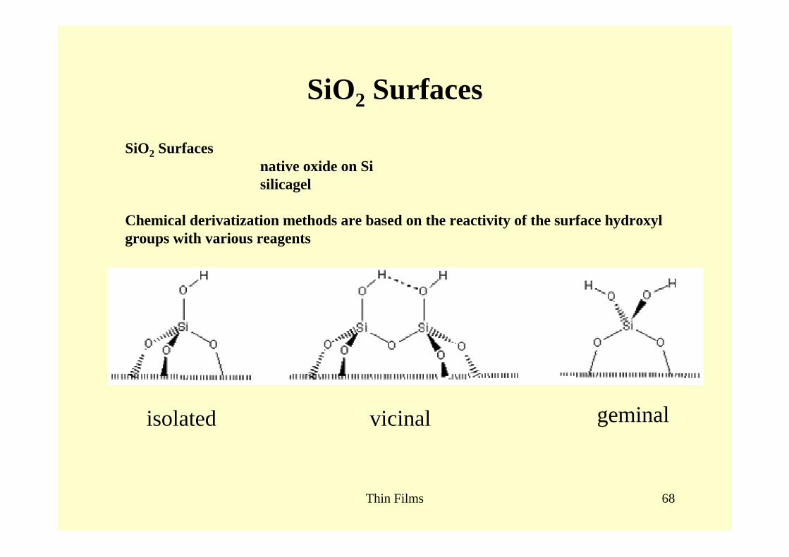
SiO2 Surfaces
SiO2 Surfacesnative oxide on Sisilicagel
Chemical derivatization methods are based on the reactivity of the surface hydroxyl groups with various reagents
isolated vicinal geminal

Thin Films 69
[O3Si]⎯OH stands for the siliceous surface 1. Grafting Reactions with trifunctional reagents, such as alkyltrichlorosilanes and trialkoxyalkylsilanes, lead to the three-fold attachment of the SiR groups. 3 [O3Si]⎯OH + Cl3SiR {[O3Si]⎯O}3SiR + 3 HCl 3 [O3Si]⎯OH + (MeO)3SiR {[O3Si]⎯O}3SiR + 3 MeOH
SiO2 Surfaces

Thin Films 70
2. Chlorination/Displacement MethodThe first step is the replacement of the Si-OH groups by morereactive Si-Cl bonds by chlorination.
[O3Si]⎯OH + SOCl2 [O3Si]⎯Cl + HCl + SO2
[O3Si]⎯OH + CCl4 [O3Si]⎯Cl + COCl2 + HCl
In the subsequent step, the surface is treated with a Grignard ororganolithium reagent with the formation of strong Si-C bonds.
[O3Si]⎯Cl + RMgCl [O3Si]⎯R + MgCl2
[O3Si]⎯Cl + RLi [O3Si]⎯R + LiCl
400 °C
SiO2 Surfaces

Thin Films 71
3. Post Modification MethodThe organic groups (R) covalently anchored to the siliceous surfaceby the two previous methods can be subsequently chemicallymodified. The most extensively developed is chemistry of 3-aminopropyl(trimethoxy)silane. A large number of chemicaltransformations of the amino moiety to other functional groups areknown.
4. Hybrid sol-gel method (co-condensation) A thin layer of a hybrid (organically modified) silica gel can bedeposited on the silica surface from a solution of TEOS and(MeO)3SiR by controlled hydrolysis and condensation.
(MeO)3SiR + (MeO)4Si + 7 H2O [O3Si]⎯R + 7 MeOH
SiO2 Surfaces
Thin Films 72
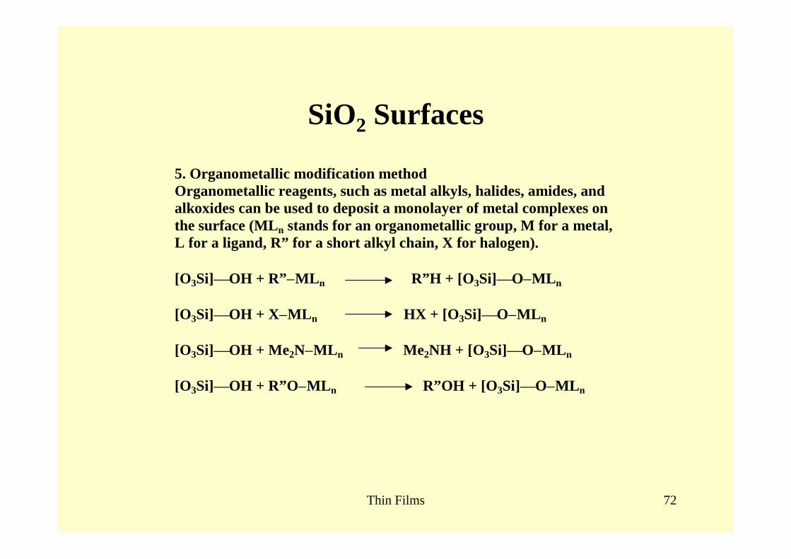
5. Organometallic modification methodOrganometallic reagents, such as metal alkyls, halides, amides, andalkoxides can be used to deposit a monolayer of metal complexes onthe surface (MLn stands for an organometallic group, M for a metal,L for a ligand, R” for a short alkyl chain, X for halogen).
[O3Si]⎯OH + R”−MLn R”H + [O3Si]⎯O−MLn
[O3Si]⎯OH + X−MLn HX + [O3Si]⎯O−MLn
[O3Si]⎯OH + Me2N−MLn Me2NH + [O3Si]⎯O−MLn
[O3Si]⎯OH + R”O−MLn R”OH + [O3Si]⎯O−MLn
SiO2 Surfaces

Thin Films 73
These organometallic moieties can serve as attachment points for further modification with long chain alcohols, thiols, carboxylic acids, phosphates, and diketonates. [O3Si]⎯O−MLn + HOR [O3Si]⎯O−MLn-1−OR + HL [O3Si]⎯O−MLn + HOOCR [O3Si]⎯O−MLn-1−OOCR + HL
SiO2 Surfaces

Thin Films 74

Thin Films 75
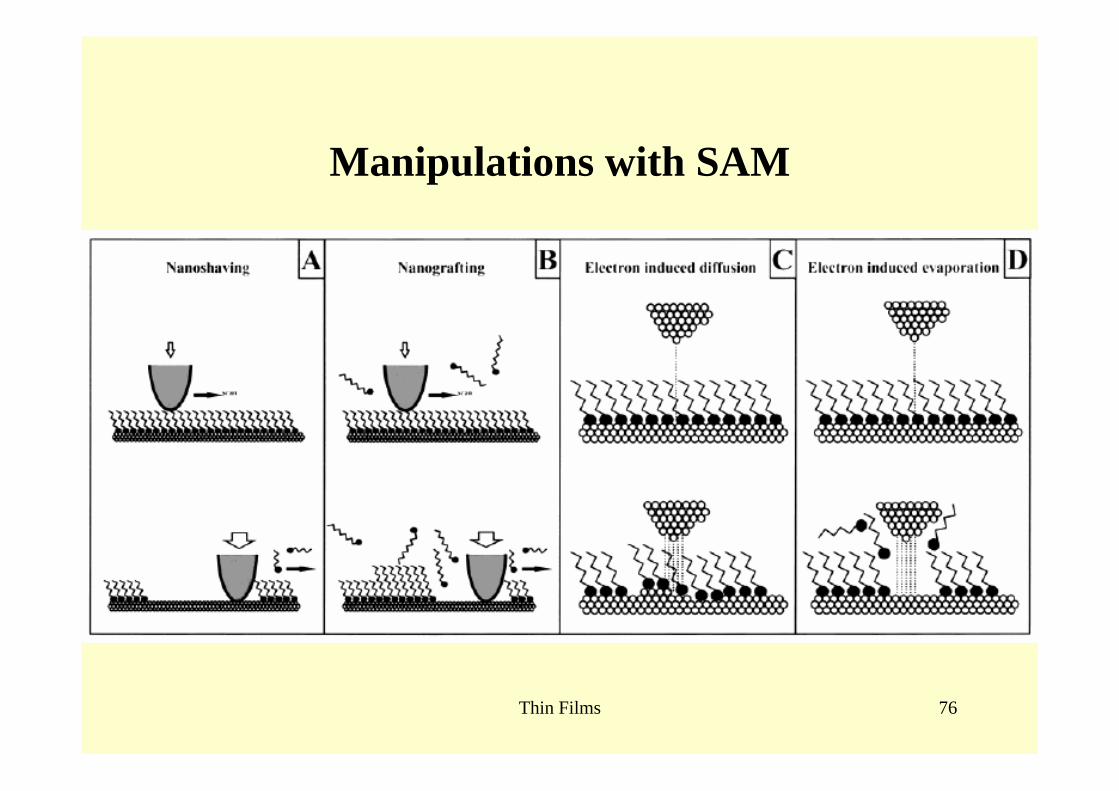
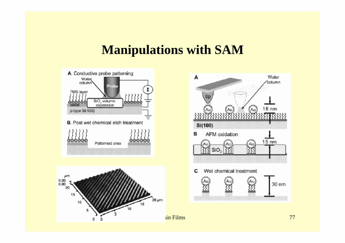
Manipulations with SAM
Thin Films 76
Manipulations with SAM
Thin Films 77
Manipulations with SAM
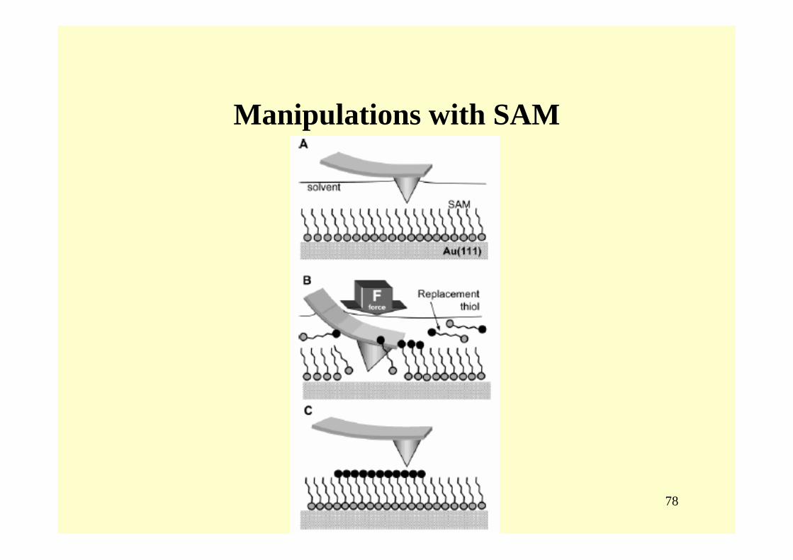
Thin Films 78
Manipulations with SAM
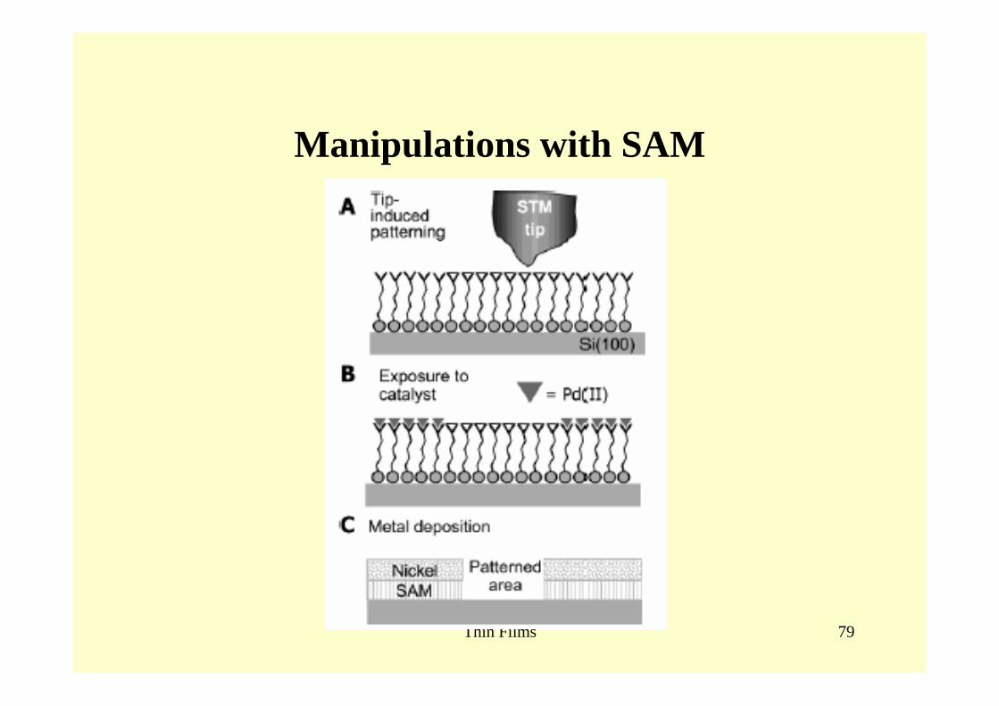
Thin Films 79
Manipulations with SAM