syspll frequency modulation - nexty ele · syspll frequency modulation ap32244 introduction to...
TRANSCRIPT

Appl icat ion Note V2.1 2016-03
TriCore™ TC2xx AURIX™ Family 32-bit
SYSPLL Frequency Modulat ion AP32244
Microcontrol lers

Edition 2016-03
Published by Infineon Technologies AG,
81726 Munich, Germany.
© 2016 Infineon Technologies AG
All Rights Reserved.
LEGAL DISCLAIMER
THE INFORMATION GIVEN IN THIS APPLICATION NOTE IS GIVEN AS A HINT FOR THE
IMPLEMENTATION OF THE INFINEON TECHNOLOGIES COMPONENT ONLY AND SHALL NOT BE
REGARDED AS ANY DESCRIPTION OR WARRANTY OF A CERTAIN FUNCTIONALITY, CONDITION OR
QUALITY OF THE INFINEON TECHNOLOGIES COMPONENT. THE RECIPIENT OF THIS APPLICATION
NOTE MUST VERIFY ANY FUNCTION DESCRIBED HEREIN IN THE REAL APPLICATION. INFINEON
TECHNOLOGIES HEREBY DISCLAIMS ANY AND ALL WARRANTIES AND LIABILITIES OF ANY KIND
(INCLUDING WITHOUT LIMITATION WARRANTIES OF NON-INFRINGEMENT OF INTELLECTUAL
PROPERTY RIGHTS OF ANY THIRD PARTY) WITH RESPECT TO ANY AND ALL INFORMATION GIVEN IN
THIS APPLICATION NOTE.
Information
For further information on technology, delivery terms and conditions and prices, please contact the nearest
Infineon Technologies Office (www.infineon.com).
Warnings
Due to technical requirements, components may contain dangerous substances. For information on the types in
question, please contact the nearest Infineon Technologies Office.
Infineon Technologies components may be used in life-support devices or systems only with the express written
approval of Infineon Technologies, if a failure of such components can reasonably be expected to cause the
failure of that life-support device or system or to affect the safety or effectiveness of that device or system. Life
support devices or systems are intended to be implanted in the human body or to support and/or maintain and
sustain and/or protect human life. If they fail, it is reasonable to assume that the health of the user or other
persons may be endangered.

SYSPLL Frequency Modulation AP32244
Application Note 3 V2.1, 2016-03
Trademarks of Infineon Technologies AG
AURIX™, C166™, CanPAK™, CIPOS™, CIPURSE™, EconoPACK™, CoolMOS™, CoolSET™,
CORECONTROL™, CROSSAVE™, DAVE™, DI-POL™, EasyPIM™, EconoBRIDGE™, EconoDUAL™,
EconoPIM™, EconoPACK™, EiceDRIVER™, eupec™, FCOS™, HITFET™, HybridPACK™, I²RF™,
ISOFACE™, IsoPACK™, MIPAQ™, ModSTACK™, my-d™, NovalithIC™, OptiMOS™, ORIGA™,
POWERCODE™; PRIMARION™, PrimePACK™, PrimeSTACK™, PRO-SIL™, PROFET™, RASIC™,
ReverSave™, SatRIC™, SIEGET™, SINDRION™, SIPMOS™, SmartLEWIS™, SOLID FLASH™,
TEMPFET™, thinQ!™, TRENCHSTOP™, TriCore™.
Other Trademarks
Advance Design System™ (ADS) of Agilent Technologies, AMBA™, ARM™, MULTI-ICE™, KEIL™,
PRIMECELL™, REALVIEW™, THUMB™, µVision™ of ARM Limited, UK. AUTOSAR™ is licensed by
AUTOSAR development partnership. Bluetooth™ of Bluetooth SIG Inc. CAT-iq™ of DECT Forum.
COLOSSUS™, FirstGPS™ of Trimble Navigation Ltd. EMV™ of EMVCo, LLC (Visa Holdings Inc.). EPCOS™
of Epcos AG. FLEXGO™ of Microsoft Corporation. FlexRay™ is licensed by FlexRay Consortium.
HYPERTERMINAL™ of Hilgraeve Incorporated. IEC™ of Commission Electrotechnique Internationale. IrDA™
of Infrared Data Association Corporation. ISO™ of INTERNATIONAL ORGANIZATION FOR
STANDARDIZATION. MATLAB™ of MathWorks, Inc. MAXIM™ of Maxim Integrated Products, Inc.
MICROTEC™, NUCLEUS™ of Mentor Graphics Corporation. MIPI™ of MIPI Alliance, Inc. MIPS™ of MIPS
Technologies, Inc., USA. muRata™ of MURATA MANUFACTURING CO., MICROWAVE OFFICE™ (MWO) of
Applied Wave Research Inc., OmniVision™ of OmniVision Technologies, Inc. Openwave™ Openwave Systems
Inc. RED HAT™ Red Hat, Inc. RFMD™ RF Micro Devices, Inc. SIRIUS™ of Sirius Satellite Radio Inc.
SOLARIS™ of Sun Microsystems, Inc. SPANSION™ of Spansion LLC Ltd. Symbian™ of Symbian Software
Limited. TAIYO YUDEN™ of Taiyo Yuden Co. TEAKLITE™ of CEVA, Inc. TEKTRONIX™ of Tektronix Inc.
TOKO™ of TOKO KABUSHIKI KAISHA TA. UNIX™ of X/Open Company Limited. VERILOG™, PALLADIUM™
of Cadence Design Systems, Inc. VLYNQ™ of Texas Instruments Incorporated. VXWORKS™, WIND RIVER™
of WIND RIVER SYSTEMS, INC. ZETEX™ of Diodes Zetex Limited.
Last Trademarks Update 2011-11-11

SYSPLL Frequency Modulation AP32244
Application Note 4 V2.1, 2016-03
Revision History
Major changes since previous revision
Date Version Changed By Change Description
13.11.2013 1.1 Steinecke Section 3.2.5.1: Variable name corrections
19.05.2014 2.0 Steinecke Updated recommended FM settings; removed calibration contents
14.03.2016 2.1 Steinecke Updated recommended FM settings to MAmax=1.0%
We Listen to Your Comments
Is there any information in this document that you feel is wrong, unclear or missing?
Your feedback will help us to continuously improve the quality of our documentation.
Please send your proposal (including a reference to this document title/number) to:

SYSPLL Frequency Modulation AP32244
Application Note 5 V2.1, 2016-03
Table of Contents
Revision History .................................................................................................................................................... 4
Table of Contents .................................................................................................................................................. 5
1 About this document ........................................................................................................................ 6 1.1 Scope and purpose ............................................................................................................................. 6 1.2 Intended audience ............................................................................................................................... 6 1.3 Abbreviations ....................................................................................................................................... 7
2 Introduction to frequency-modulated clocks ................................................................................. 9 2.1 Hints on clock Frequency Modulation ................................................................................................. 9 2.2 TriCore™ AURIX™ TC2xx SYSPLL Frequency Modulation ............................................................ 12 2.2.1 General clocking scheme ............................................................................................................. 12 2.2.2 Modulation parameters ................................................................................................................ 13 2.2.2.1 Modulation scheme and modulation period ............................................................................ 13 2.2.2.2 Modulation Amplitude ............................................................................................................. 13
3 Configuration of the SYSPLL Frequency Modulation ................................................................. 14 3.1 Summary of recommended system clock Frequency Modulation setting......................................... 14 3.2 Recommended register settings for SYSPLL initialization ................................................................ 14 3.2.1 PLLCON0 settings for SYSPLL ................................................................................................... 15 3.2.2 PLLCON1 settings for SYSPLL ................................................................................................... 16 3.2.3 PLLCON2 settings for SYSPLL ................................................................................................... 17 3.2.4 Activating system clock Frequency Modulation ........................................................................... 18 3.3 Parameter table for other SYSPLL parameters ................................................................................ 19 3.4 Modulation-related effects ................................................................................................................. 19 3.4.1 Introduction to modulation-related terms ..................................................................................... 19 3.4.2 Introduction to accumulated jitter ................................................................................................. 20 3.4.3 Long-term accumulated jitter ....................................................................................................... 21 3.4.4 Short-term accumulated jitter and time interval error ................................................................... 24 3.4.4.1 MTIE values for different data rates ........................................................................................ 27 3.4.5 Electromagnetic Emission ............................................................................................................ 28 3.4.6 Clock frequency accuracy ............................................................................................................ 34

SYSPLL Frequency Modulation AP32244
About this document
Application Note 6 V2.1, 2016-03
1 About this document
1.1 Scope and purpose
Frequency-modulated clocks are an efficient way to significantly reduce Electromagnetic Emission (EME).
Unfortunately, clock modulation implies clock edge offset (accumulated jitter, time interval error) which might
inhibit the correct operation of asynchronous data interfaces. The AURIX™ System-PLL (SYSPLL) solves this
problem by providing a clock Frequency Modulation technique which reduces the accumulated jitter while
providing the full emission reduction (as it is known), from existing spread-spectrum systems. The Modulation
Amplitude is configurable by a 10-bit field. The programmed nominal Modulation Amplitude (MANOM) should not
exceed 1.5% in order to not exceed the microcontrollers’ operating range. Due to constraints of data interfaces,
the programmed nominal Modulation Amplitude (MANOM) should be maximal 1.0%, as specified in the data
sheet. MANOM = 1.0% ist the recommended value. Nevertheless, some descriptions in this Application Note are
provided for values other than 1.0% for information purpose.
Document features
Chapter 2
- General hints on clock Frequency Modulation
- Modulation parameters: modulation scheme, modulation period, Modulation Amplitude
Chapter 3
- Programming the TriCore™ AURIX™ TC2xx SYSPLL for Frequency Modulation
- Control register settings for various Frequency Modulation configurations
- Lookup tables for different SYSPLL configurations
- Behavior of modulation-related parameters:
- Long-term accumulated jitter
- Short-term accumulated jitter (Maximum Time Interval Error MTIE)
- Electromagnetic Emission
- Mean frequency deviation
1.2 Intended audience
The information contained in this application note addresses system architects who are looking for measures to
reduce EME when using AURIX™ microcontrollers. In particular, software developers will find useful information
on how to initialize and configure the AURIX™ Frequency Modulation.

SYSPLL Frequency Modulation AP32244
About this document
Application Note 7 V2.1, 2016-03
1.3 Abbreviations
Table 1
Abbreviation Definition
BISS IC EMC Test Specification.
Download from: http://www.zvei.org/en/association/publications/Pages/Generic-IC-EMC-
Test-Specification-english.aspx
Center-spread Symmetric Frequency Modulation around a center frequency.
EMC Electromagnetic Compatibility
The ability of a system to not disturb any other systems and being not disturbed by other
systems.
EME Electromagnetic Emission
RF noise generated by (synchronous) switching activity.
FM Frequency Modulation
A periodic change of a clock rate.
FMPLL Frequency-Modulated Phase-Locked Loop
An emission-reducing clock generator for ICs.
fCPUx Operating clock for the microcontroller’s central processing unit x.
fMOD Modulation frequency
Determines the duration of one full modulation period.
fOSC Oscillator frequency
Determined by the crystal connected to the microcontroller’s oscillator.
fPLL SYSPLL output frequency after Kx-divider, used as input clock for the clock domain dividers.
fREF SYSPLL input frequency after P-divider; i.e. fOSC / P.
fVCO VCO frequency inside the SYSPLL before Kx-divider; i.e. fOSC / P · N.
fVCO_MEAN Mean VCO frequency over more than one modulation cycle.
JACC Accumulated jitter
The maximum expected offset of the real clock edge over an infinite time towards the nominal
(unmodulated) clock edge without noise.
Note:
1. Accumulated jitter is abbreviated as JTOT in the data sheets.
2. It is important to distinguish between long-term and short-term accumulated jitter.
Kx K-divider (stands for K1, K2 or K3) which divides fVCO in order to generate internal system
clocks.
LF Low Frequency
Audio-range frequency.
MA Modulation Amplitude
The resulting range of real VCO frequency is half frequency shift between minimum and
maximum frequency; for a symmetrical center-spread modulation this is the frequency shift
between the center frequency and the maximum/minimum frequency, respectively.
MANOM Nominal Modulation Amplitude
i.e. the value programmed by the user software

SYSPLL Frequency Modulation AP32244
About this document
Application Note 8 V2.1, 2016-03
Abbreviation Definition
MAREAL Real Modulation Amplitude
i.e. the physical value resulting from the programmed MANOM value
MTIE Maximum Time Interval Error
The maximum expected offset of the real clock edge towards the nominal (unmodulated) clock
edge without noise after a defined time interval.
N N-divider (clock multiplier) value in the SYSPLL.
P P-divider for oscillator clock in the SYSPLL.
PVT Fabrication process window (P)
Operating supply voltage range (V)
Operating temperature range (T)
RF Radio Frequency
High frequency used as radio carrier.
RGAIN A value to be programmed which depends on the Modulation Amplitude (MA).
SYSPLL System-PLL (Phase Locked Loop)
Can be configured for clock Frequency Modulation; called “PLL” in the User’s Manual.
TMOD Duration of one modulation period.
TREF Duration of one SYSPLL reference clock (oscillator frequency divided by P).
TVCO_MEAN Mean VCO clock period over more than one modulation cycle.
Upspread Frequency Modulation above a nominal frequency.
VCO Voltage-Controlled Oscillator
Used in the SYSPLL to compensate frequency drifts of the high-frequency clock.
VDD Core supply voltage
Powering the digital logic of the microcontroller.
VDDP Pad supply voltage
Powering the I/O stages of the microcontroller.

SYSPLL Frequency Modulation AP32244
Introduction to frequency-modulated clocks
Application Note 9 V2.1, 2016-03
2 Introduction to frequency-modulated clocks
2.1 Hints on clock Frequency Modulation
Frequency-modulated clocks are also known as spread spectrum clocks. They are well established in
communication techniques. FM radio uses an RF carrier which is modulated by the LF audio signal. As a result,
the carrier frequency moves around its nominal frequency. The Modulation Amplitude is defined by the LF signal
amplitude, while the modulation frequency is identical to the LF frequency. Both parameters vary over time.
Frequency Modulation can be used to intentionally spread the carrier energy around the nominal carrier
frequency. Since the overall energy stays constant, the carrier energy is distributed over a frequency band
instead of staying in one discrete frequency. As a result, the peak emission caused by the carrier is reduced.
Typical applications of this spread-spectrum technique are EMC-critical applications such as automotive
electronic control units.
Although 20 dB emission reductions can be reached using spread-spectrum clocks, this technique is not yet
very common for automotive microcontroller systems. The main reason is the danger of inhibiting real-time
functions such as asynchronous data communication or timer capture sequences. To understand this danger,
let us have a closer look at the determining characteristics for frequency-modulated clocks.
Similar to radio FM, a frequency-modulated microcontroller clock is controlled by its modulation frequency (fMOD)
and it’s Modulation Amplitude (MA).
Typically, the modulation frequency should be selected to be approximately a factor of 1000 below the clock
frequency. This distance is required by the FMPLL (FM Phase Locked Loop) filter in order to prevent the
modulation clock from being coupled to the VCO. A typical fMOD range is from 50 kHz to 200 kHz.
The MA defines the amount of frequency shift in one direction from the mean clock frequency (“carrier”). An MA
value of 1% on a 100 MHz clock means a frequency variation between 99 MHz and 101 MHz.
Figure 1 FMPLL function
Higher values of MA and lower values of fMOD lead to less EME. Bigger MA values lead to wider sidebands
where the carrier energy is distributed.

SYSPLL Frequency Modulation AP32244
Introduction to frequency-modulated clocks
Application Note 10 V2.1, 2016-03
Slower fMOD values lead to a smoother distribution of sideband energy; i.e. any discrete sideband frequency
is activated less often.
Unfortunately, the trend of less emission together with higher MA and lower fMOD is accompanied by an
increasing accumulated jitter. This parameter is also known as Maximum Time Interval Error (MTIE). It means
the amount of time shift between the unmodulated clock edges and the modulated clock edges over a certain
time interval.
For a center-spread triangular modulation, JACC-FM is a function of the modulation frequency fMOD and the
Modulation Amplitude MA, according to Equation 1:
][
[%]2500][_
kHzf
MAnsJ
MOD
FMACC
(Equation 1)
The JACC-FM value which is determined by the Frequency Modulation (FM) ranges from approximately 20 ns to
well above 100 ns for typical FM settings.
In order to guarantee the reliable function of asynchronous interfaces and real-time data capture functions, the
MTIE along an asynchronous frame has to stay below a certain limit defined for these interfaces. Timer modules
and analog-to-digital converters may also be sensitive towards modulated clocks. This requirement for a small
accumulated jitter cannot be fulfilled by a standard triangular modulation unless the Modulation Amplitude is set
significantly small, resulting in insufficient emission reduction.
The following figure shows an example for fPLL = 100 MHz, fMOD = 100 kHz, MA = 1 %, resulting in an
accumulated jitter of 25 ns.

SYSPLL Frequency Modulation AP32244
Introduction to frequency-modulated clocks
Application Note 11 V2.1, 2016-03
Figure 2 Important FM parameters

SYSPLL Frequency Modulation AP32244
Introduction to frequency-modulated clocks
Application Note 12 V2.1, 2016-03
2.2 TriCore™ AURIX™ TC2xx SYSPLL Frequency Modulation
2.2.1 General clocking scheme
AURIX™ microcontrollers offer several clock domains. Of those domains, SYSPLL can be modulated:
Table 2 Available clock domains
Domain PLL Modulation Master clocks Purpose
System clock SYSPLL available SRI, SPB Operate CPU and peripherals
FlexRay clock ERAYPLL not available ERAY Operate jitter-critical peripherals
HSSL HSCTPLL not available HSCT Operate high-speed communication tunnel
AGBT AGBTPLL not available AGBT Operate gigabit communication channel
Backup clock n/a not available BACKUP Boot and fall-back clock in case of clock failure
Peripheral functions which may have trouble meeting timing specifications when operated with a modulated
clock, are either hard-connected to an unmodulated clock (as listed above), or their clock source can be
selected among modulated and unmodulated clock sources.
Note: For further details please refer to the AURIX™ User Manual.
Table 3 Available clock sources for peripherals
Module Modulated clock source Unmodulated clock source
ERAY no yes
HSSL no yes
AGBT no yes
MultiCAN+ yes yes
ASCLIN yes yes
QSPI yes yes
I2C yes yes
PSI5(S) yes yes
MSC yes yes
DSADC yes yes
VADC yes yes
GTM yes yes
STM yes yes
Note: All other peripherals are operated with the modulated clock whenever modulation is enabled.

SYSPLL Frequency Modulation AP32244
Introduction to frequency-modulated clocks
Application Note 13 V2.1, 2016-03
2.2.2 Modulation parameters
2.2.2.1 Modulation scheme and modulation period
AURIX™ microcontrollers use a random Frequency Modulation scheme for the SYSPLL.
The modulation sequence consists of 215-1 = 32767 pseudo-random values.
It uses the crystal oscillator clock divided by P as a reference clock.
After every reference clock period TREF, the SYSPLL VCO is modulated with the next pseudo-random value.
TREF = P / fOSC (Equation 2)
Taking as an example a Crystal oscillator clock fOSC = 20 MHz and P = 2.
The resulting reference clock period is TREF = P / fOSC = 100 ns.
The complete “modulation period”, consisting of 32767 reference clock periods, takes 3.2767 ms.
Higher crystal frequency or a smaller P divider value reduces the modulation period accordingly. These are the
only ways to change the modulation period.
Note: The length of this modulation period is not important. Because of the random type of modulation, the
accumulated jitter value saturates a long time before one complete modulation period is over. It has been
verified by measurement that the long-term accumulated jitter value is reached after approximately 300
ns.
2.2.2.2 Modulation Amplitude
AURIX™ microcontrollers accept a maximum MA of 2.0% for the SYSPLL. This value results in a +/- 2%
frequency deviation of the system clock around its nominal value, given by:
fPLL = fOSC / P · N / K2 (Equation 3)
This maximum MA should never be exceeded.
The main reason to use Frequency Modulation is for the related EME reduction. Higher MA causes less EME.
On the other hand, the accumulated jitter rises with higher MA. However, the modulation scheme determines
the resulting accumulated jitter. For instance, triangular modulation causes high accumulated jitter, as can be
calculated using Equation 1. The long-term mean frequency is not influenced by the Frequency Modulation.
The SYSPLL in AURIX™ microcontrollers implements a “Random Frequency Modulation”. It provides
significantly less accumulated jitter values than known from triangular modulation schemes.
Due to an intrinsic design-related temperature drift of the MA, the physical real Modulation Amplitude MAREAL
deviates from the nominal Modulation Amplitude MANOM which is programmed by the user.
MAREAL varies with the fabrication window, supply voltage and temperature (“PVT variation”). Over the whole
fabrication window and operating temperature range, the real Modulation Amplitude MAREAL varies around the
programmed nominal MANOM, according to Equations 4 and 5.
The lowest value is (at junction temperature Tj = 170 °C):
MAREAL_MIN = 0.5 · MANOM (Equation 4)
The highest value is (at junction temperature Tj = -40 °C):
MAREAL_MAX = 1.33 · MANOM (Equation 5)
The programmed MANOM value should consider:
1. Avoid the real modulation amplitude to exceed the maximal allowed value of 2.0% (Condition 1)
2. Avoid the long-term accumated jitter to exceed the specified value of 11.5 ns (Condition 2)
Condition 1 is met by any chosen value of MANOM up to 1.5%, considering the drift numbers given by Equations
4 and 5.
Condition 2 is met by any chosen value of MANOM up to 1.0%, considering the diagram in Figure 9.
Lower MANOM values increase the EME, and a higher MANOM values increase the accumulated jitter.
SYSPLL Frequency Modulation AP32244
Configuration of the SYSPLL Frequency Modulation
Application Note 14 V2.1, 2016-03
3 Configuration of the SYSPLL Frequency Modulation
3.1 Summary of recommended system clock Frequency Modulation setting
The recommendation is to operate the SYSPLL with the following parameters:
fOSC = 20 MHz
P = 2
N = 60
K2 = 3 (for CPU clock 200 MHz) or K2 = 2 (for CPU clock 300 MHz)
MANOM = 1.0%
Other configurations are of course possible. However, the programmed nominal Modulation Amplitude MANOM
should not exceed 1.0% in order to stay below the specified maximal long-term accumulated jitter of 11.5 ns
under all PVT conditions.
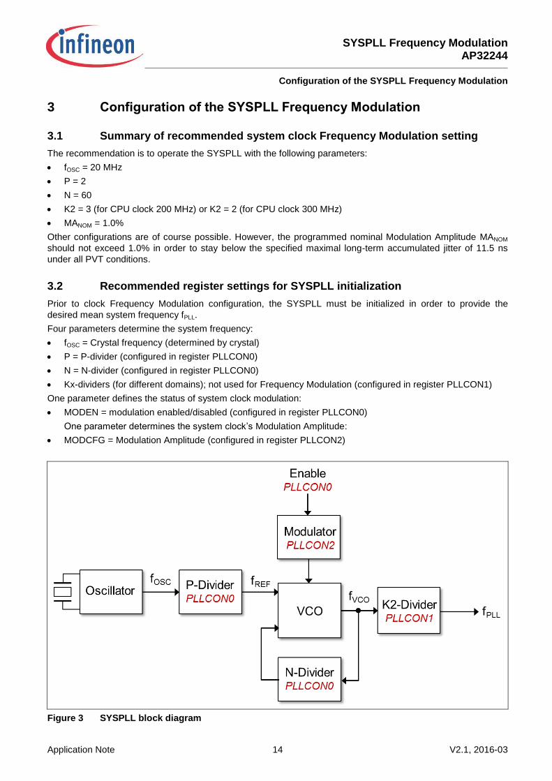
3.2 Recommended register settings for SYSPLL initialization
Prior to clock Frequency Modulation configuration, the SYSPLL must be initialized in order to provide the
desired mean system frequency fPLL.
Four parameters determine the system frequency:
fOSC = Crystal frequency (determined by crystal)
P = P-divider (configured in register PLLCON0)
N = N-divider (configured in register PLLCON0)
Kx-dividers (for different domains); not used for Frequency Modulation (configured in register PLLCON1)
One parameter defines the status of system clock modulation:
MODEN = modulation enabled/disabled (configured in register PLLCON0)
One parameter determines the system clock’s Modulation Amplitude:
MODCFG = Modulation Amplitude (configured in register PLLCON2)
Figure 3 SYSPLL block diagram

SYSPLL Frequency Modulation AP32244
Configuration of the SYSPLL Frequency Modulation
Application Note 15 V2.1, 2016-03
3.2.1 PLLCON0 settings for SYSPLL
Figure 4 SYSPLL-relevant register PLLCON0
The Frequency Modulation is controlled completely digitally and is therefore reliable in respect to the mean
frequency deviation, the Modulation Amplitude, and the accumulated jitter.
The Frequency Modulation is turned off after reset and must be explicitly enabled by setting the bit
PLLCON0.MODEN.
Before doing so, the SYSPLL has to be initialized in order to provide the desired mean system frequency fPLL
and the desired Modulation Amplitude.
Recommended settings
PDIV = 0001b ( P = 2)
NDIV = 0111011b ( N = 60)
MODEN =1 ( enable SYSPLL clock modulation)

SYSPLL Frequency Modulation AP32244
Configuration of the SYSPLL Frequency Modulation
Application Note 16 V2.1, 2016-03
3.2.2 PLLCON1 settings for SYSPLL
Figure 5 SYSPLL-relevant register PLLCON1
Recommended settings
K2DIV = 0010b ( K2 = 3 for fPLL = 200 MHz)
K2DIV = 0001b ( K2 = 2 for fPLL = 300 MHz)
K1DIV and K3DIV according to user system requirements

SYSPLL Frequency Modulation AP32244
Configuration of the SYSPLL Frequency Modulation
Application Note 17 V2.1, 2016-03
3.2.3 PLLCON2 settings for SYSPLL
The modulation parameters need to be programmed in the register PLLCON2.
PLLCON2 contains the bit pattern RGAIN for the MA in the 10-bit field MODCFG[9:0].
Figure 6 SYSPLL clock Frequency Modulation relevant register PLLCON2
For any desired Modulation Amplitude MANOM, the corresponding bit-field MODCFG[9:0] can be calculated
considering oscillator frequency fOSC, P-divider P and N-divider N, according to Equation 6:
MODCFG[9:0] = RGAIN = HEX (64 • MANOM/100 • fOSC/P • N/3.6) ; units: MA [%] , fOSC [MHz] (Equation 6)
Example for recommended Modulation Amplitude MA = 1.0%:
Let fOSC = 20 MHz; P = 2; N = 60 MODCFG[9:0] = 0001101010b = 06Ah
The programmed nominal Modulation Amplitude can also be calculated from the bit-field value MODCFG[9:0]
as follows:
MANOM = 5.625 • DEC(MODCFG[9:0]) • P / (fOSC • N) (Equation 7)

SYSPLL Frequency Modulation AP32244
Configuration of the SYSPLL Frequency Modulation
Application Note 18 V2.1, 2016-03
3.2.4 Activating system clock Frequency Modulation
After having completed all other SYSPLL configurations, the system clock Frequency Modulation is activated by
setting the MODEN bit (= bit 2) in register PLLCON0.
Whether Frequency Modulation is active or not is indicated by the status bit MODRUN in the register PLLSTAT:
Figure 7 SYSPLL clock Frequency Modulation relevant register PLLSTAT
SYSPLL Frequency Modulation AP32244
Configuration of the SYSPLL Frequency Modulation
Application Note 19 V2.1, 2016-03
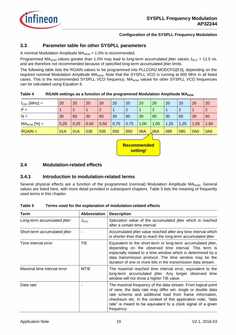
3.3 Parameter table for other SYSPLL parameters
A nominal Modulation Amplitude MANOM = 1.0% is recommended.
Programmed MANOM values greater than 1.0% may lead to long-term accumulated jitter values JACC > 11.5 ns,
and are therefore not recommended because of specified long-term accumulated jitter limits.
The following table lists the RGAIN values to be programmed into PLLCON2.MODCFG[9:0], depending on the
required nominal Modulation Amplitude MANOM. Note that the SYSPLL VCO is running at 600 MHz in all listed
cases. This is the recommended SYSPLL VCO frequency. MANOM values for other SYSPLL VCO frequencies
can be calculated using Equation 6.
Table 4 RGAIN settings as a function of the programmed Modulation Amplitude MANOM
fOSC [MHz] = 20 20 20 20 20 20 20 20 20 20 20 20
P = 1 2 1 2 1 2 1 2 1 2 1 2
N = 30 60 30 60 30 60 30 60 30 60 30 60
MANOM [%] = 0,25 0,25 0,50 0,50 0,75 0,75 1,00 1,00 1,25 1,25 1,50 1,50
RGAIN = 01A 01A 035 035 050 050 06A 06A 085 085 0A0 0A0
3.4 Modulation-related effects
3.4.1 Introduction to modulation-related terms
Several physical effects are a function of the programmed (nominal) Modulation Amplitude MANOM. General
values are listed here, with more detail provided in subsequent chapters. Table 5 lists the meaning of frequently
used terms in this chapter.
Table 5 Terms used for the explanation of modulation-related effects
Term Abbreviation Description
Long-term accumulated jitter JACC Saturation value of the accumulated jitter which is reached
after a certain time interval
Short-term accumulated jitter - Accumulated jitter value reached after any time interval which
is shorter than that to reach the long-term accumulated jitter
Time interval error TIE Equivalent to the short-term or long-term accumulated jitter,
depending on the observed time interval. This term is
especially related to a time window which is determined by a
data transmission protocol. The time window may be the
duration of one or more bits in the transmission data stream.
Maximal time interval error MTIE The maximal reached time interval error, equivalent to the
long-term accumulated jitter. Any longer observed time
window will not show a higher TIE value.
Data rate - The maximal frequency of the data stream. From logical point
of view, the data rate may differ wrt. single or double data
rate scheme and additional load from frame information,
checksum etc. In the context of this application note, “data
rate” is meant to be equivalent to a clock signal of a given
frequency.
Recommended
setting!

SYSPLL Frequency Modulation AP32244
Configuration of the SYSPLL Frequency Modulation
Application Note 20 V2.1, 2016-03
The SYSPLL in the Infineon AURIX™ microcontrollers was designed to provide an emission reduction similar to
a triangular modulation, while at the same time limiting the accumulated jitter.
The following are the target values of the SYSPLL clock Frequency Modulation, using the recommended value
MANOM = 1.0%. The values have been verified by measurements over full PVT variation.
The system clock fPLL generated by the SYSPLL is spread around its nominal center value:
- fPLLmin = (1-MAREAL) · fOSC / P · N / K2 ; 0.5 · MANOM < MAREAL < 1.33 · MANOM
(Equation 8)
- fPLLmax = (1+MAREAL) · fOSC / P · N / K2 ; 0.5 · MANOM < MAREAL < 1.33 · MANOM
(Equation 9)
- All other clocks derived from the SYSPLL are spread accordingly.
Long-term accumulated jitter JACC ≤ 11.5 ns. It is valid for time intervals greater than approximately 1 µs –
equivalent to a data rate of 1 MHz, after which a “saturation” condition is met.
For fast data communication (i.e. data rates higher than approximately 200 kHz), the short-term
accumulated jitter needs to be considered. It is equivalent to the Maximum Time Interval Error MTIE and
smaller than the long-term accumulated jitter:
- MTIE < 1.5 ns @ Data rates faster than 25 MHz
- MTIE < 3 ns @ Data rates faster than 10 MHz
- MTIE < 5 ns @ Data rates faster than 5 MHz
- MTIE < 8 ns @ Data rates faster than 3 MHz
- MTIE < 9.5 ns @ Data rates faster than 1 MHz
The mean system clock accuracy is < 0.001%.
The emission reduction compared to unmodulated SYSPLL operation is:
- 3 dB @ peripheral clock (typically fPLL/2 or fPLL//3)
- 9 dB @ CPU clock (typically fPLL)
- 15 dB @ higher harmonics of CPU and peripheral clocks
3.4.2 Introduction to accumulated jitter
According to Equations 4 and 5, the real Modulation Amplitude MAREAL has:
minimum value at high temperature MAREAL_MIN = 0.5 · MANOM (at Tj = 180 °C)
maximum value at low temperature MAREAL_MAX = 1.33 · MANOM (at Tj = -50 °C)
Less accumulated jitter at high temperature would cause higher emission, but this effect is partly compensated
by reduced transistor switching speed at high temperature, which leads to lower emission.
Summarized, the deviation of the real Modulation Amplitude over temperature does not have significant
influence on Electromagnetic Emission. However, care must be taken that the deviation of the accumulated jitter
is acceptable by all timing-related microcontroller functions such as data transmission and timer.
In this context it is important to distinguish between long-term and short-term accumulated jitter. The long-term
accumulated jitter is the saturation value of clock edge shift caused by the clock modulation. It is reached after
approximately 5 µs.

SYSPLL Frequency Modulation AP32244
Configuration of the SYSPLL Frequency Modulation
Application Note 21 V2.1, 2016-03
Figure 8 Short-term and long-term accumulated jitter ranges of a measured example
All timings longer than 1 µs – equivalent to data rates higher than 1 MHz – should be assessed using the long-
term accumulated jitter value. Shorter timings should be assessed using the short-term accumulated jitter. Both
jitter parameters have been evaluated along with different Modulation Amplitudes. The results are described in
subsequent chapters.
The evaluation measurements have been performed over the full PVT variation of the microcontrollers (P =
process variation; i.e. fabrication window; V = supply voltages; T = operating temperature). Therefore the results
shown within this document can be treated as worst-case values.
3.4.3 Long-term accumulated jitter
The accumulated jitter JACC rises with MANOM. It is important to distinguish between the long-term JACC and the
short-term JACC. The short-term JACC is related to the Maximum Time Interval Error MTIE, which describes the
maximum drift of clock edges after one or more unsynchronized bits of a data transmission. This MTIE is
identical to the short-term JACC for the same time.
The long-term accumulated jitter is the maximum value of the accumulated jitter for all time intervals; i.e. over a
time interval of arbitrary length. It depends on the programmed Modulation Amplitude MANOM and the PVT
operating conditions. The worst-case, long-term accumulated jitter stays below 11.5 ns for the recommended
setting of the nominal Modulation Amplitude MANOM ≤ 1.0% and any PVT variation within the specified operating
ranges, see Figure 9. Any MANOM ≤ 1.0% results in an even lower long-term accumulated jitter. Figure 10 shows
similar information for MA = 1.5%for comparison, resulting in max. 15.5 ns long-term accumulated jitter.

SYSPLL Frequency Modulation AP32244
Configuration of the SYSPLL Frequency Modulation
Application Note 22 V2.1, 2016-03
Figure 9 MAREAL and long-term JACC trends for full PVT variation using recommended MANOM = 1.0%
Figure 10 MAREAL and long-term JACC trends for full PVT variation using MANOM = 1.5%

SYSPLL Frequency Modulation AP32244
Configuration of the SYSPLL Frequency Modulation
Application Note 23 V2.1, 2016-03
Table 6 Long-term accumulated jitter (JACC) spec violation as function of MA overfull PVT variation
MANOM Measured JACC JACC spec.
21 ns
JACC spec.
15.5 ns
JACC spec.
11.5 ns
JACC spec.
9 ns
JACC spec.
6 ns
0.5 % <6 ns OK OK OK OK OK
0.8 % <9 ns OK OK OK OK FAIL
1.0 % <11.5 ns OK OK OK FAIL FAIL
1.5 % <16 ns OK OK FAIL FAIL FAIL
2.0 % <21 ns OK FAIL FAIL FAIL FAIL
The following diagram shows the long-term accumulated jitter trend, depending on the selected nominal
Modulation Amplitude MANOM and the SYSPLL divider settings P and N. In all cases, the oscillator frequency is
20 MHz and the SYSPLL VCO frequency is 600 MHz.
Figure 11 Long-term JACC trends as function of MANOM and SYSPLL dividers
The blue and red lines indicate the jitter values for a nominal device (centered fabrication window) operated
under nominal conditions (room temperature, nominal supply voltages).
The jitter value deviation for different P and N divider settings is clearly visible. The random frequency modulator
takes the crystal oscillator clock divided by P as a reference clock.
With every reference clock period the VCO of the SYSPLL is modulated by a new value. It is apparent therefore,
that a smaller P value leads to less accumulated jitter. On the other hand, emission increases accordingly.
Since the motivation for PLL clock spreading is reaching lowest emission, we recommend to use the divider
values P = 2 and N = 60 for the modulated SYSPLL.

SYSPLL Frequency Modulation AP32244
Configuration of the SYSPLL Frequency Modulation
Application Note 24 V2.1, 2016-03
The magenta line indicates the maximum jitter values occurring over full PVT (fabrication window, specified
operating supply voltage range, specified operating temperature range) variation. The JACC values in Table 6
are taken from this limit line.
3.4.4 Short-term accumulated jitter and time interval error
For short time intervals in the range between zero and approximately 300 ns, the accumulated jitter is
considerably smaller than the long-term jitter value. This is especially important when the Maximum Time
Interval Error (MTIE) for data protocols is considered.
The MTIE describes the edge shift between an ideally constant clock and a jittered or modulated clock. It is
equivalent to the short-term accumulated jitter. Considering the MTIE is essential to assess the protocol timings
of asynchronous data interfaces or other time-critical functions.
According to the following two diagrams, the short-term accumulated jitter covers time intervals shorter than 500
ns, which is equivalent to data rates faster than 2 MHz.
Note: Data protocols may specify data frames. The communication channel is re-synchronized after one frame.
Example calculation
The data rate is assumed to be 50 MHz; i.e. one bit lasts for 20 ns.
One data frame accumulates 10 data bits.
10 · 20 ns = 200 ns.
This interval is equivalent to a data rate of 5 MHz.
In the diagram below, for 1.0% nominal Modulation Amplitude (blue line), an MTIE of 5 ns is assigned to a 5
MHz data rate. This is less than half of the maximal long-term accumulated jitter (11.5 ns) for 1.0% nominal
Modulation Amplitude. This judgement of the individual MTIE values for the data interfaces is recommended in
order to determine which highest Modulation Amplitude can be accepted for the correct operation of all data
interfaces.
Long-term accumulated jitter values apply to low-speed data rates below ca. 1 MHz. For these data rates, the
MTIE is approximately equal to the long-term accumulated jitter for the selected Modulation Amplitude.
Figure 12 illustrates the MTIE trend for data rates from 10 kHz to 100 MHz, depending on the selected nominal
Modulation Amplitude MANOM. The SYSPLL divider settings are: fOSC = 20 MHz, P = 2, N = 60, K2 = 3. For faster
data rates, the MTIE becomes significantly lower than the long-term accumulated jitter.

SYSPLL Frequency Modulation AP32244
Configuration of the SYSPLL Frequency Modulation
Application Note 25 V2.1, 2016-03
Figure 12 Absolute values for short-term accumulated jitter = Maximum Time Interval Error (MTIE)
Protocols using slow data rates accept typically a higher absolute MTIE value. Therefore it makes sense to
introduce the “Relative MTIE” which is the ratio between the “Absolute MTIE” at this data rate and the duration
of one bit at this data rate. Although the absolute MTIE values increase with slower data rates, the relative MTIE
becomes smaller with slower data rates, indicating that a dedicated MTIE value is less critical for low-speed
data communication. For the example above, the 7 ns short-term jitter is equivalent to 3.5 % of the 200 ns time
interval.
Figure 13Figure 12 illustrates the trend of the MTIE to data bit length ratio for data rates from 10 kHz to 100
MHz, depending on the selected nominal Modulation Amplitude MANOM. The SYSPLL divider settings are: fOSC =
20 MHz, P = 2, N = 60, K2 = 3. For slower data rates, this ratio gets significantly low, indicating that slow data
transfers should not violate the underlying protocol. High data rates imply a higher ratio and should be
investigated carefully.

SYSPLL Frequency Modulation AP32244
Configuration of the SYSPLL Frequency Modulation
Application Note 26 V2.1, 2016-03
Figure 13 Ratio values for Maximum Time Interval Error (MTIE) divided by data bit length

SYSPLL Frequency Modulation AP32244
Configuration of the SYSPLL Frequency Modulation
Application Note 27 V2.1, 2016-03
3.4.4.1 MTIE values for different data rates
A variety of data rates along with their absolute MTIE values and MTIE to bit length ratio numbers are listed in
Table 7 for different MANOM values between 1.0% and 2.0%.
Table 7 Maximum Time Interval Error for different data rates and Modulation Amplitudes

SYSPLL Frequency Modulation AP32244
Configuration of the SYSPLL Frequency Modulation
Application Note 28 V2.1, 2016-03
3.4.5 Electromagnetic Emission
Electromagnetic Emission (EME) is measured under nominal PVT conditions; i.e. centered fabrication lot,
nominal supply voltages and room temperature. These conditions lead to approximately 80°C junction
temperature for typical microcontroller operation, and the real Modulation Amplitude MAREAL is ca. 20% lower
than the programmed Modulation Amplitude MANOM.
Figure 14 Deviation of MA over junction temperature for a POR device supplied by nominal voltages
EME decreases with higher temperature because CMOS transistors become slower. This trend is partially
compensated by the reduced MA towards high temperature. Therefore the EME is expected to stay
approximately stable over temperature.
The lowest emission (especially at low-order system clock harmonics) is reached for SYSPLL divider settings
P = 2, N = 60, K2 = 3. SYSPLL divider settings P = 1, N = 30, K2 = 3 lead to significantly higher emission.
This trend is the opposite of the accumulated jitter trend. The long-term accumulated jitter is higher for divider
settings P = 2, N = 60, K2 = 3.
Considering the fact that most microcontroller timings are related to the short-term accumulated jitter which is
significantly smaller than the long-term accumulated jitter, low emission should get priority over small long-term
jitter.
Figure 15 shows the EME trend depending on the SYSPLL divider settings P and N. The parameters are:
oscillator frequency is 20 MHz; nominal Modulation Amplitude MANOM = 1.5%.
The similar behaviour can be assumed for MANOM = 1.0%.
Due to the Modulation Amplitude deviation at nominal PVT conditions (i.e. emission measurement conditions),
the following translation between MANOM and MAREAL is valid:
Table 8 Relationship between nominal and real Modulation Amplitudes
MANOM [%] MAREAL [%]
0.5 0.4
1.0 0.8
1.25 1.0
1.5 1.2

SYSPLL Frequency Modulation AP32244
Configuration of the SYSPLL Frequency Modulation
Application Note 29 V2.1, 2016-03
Figure 15 EME trends as function of SYSPLL dividers
For MANOM = 1.5% (MAREAL = 1.2%), an emission reduction of up to 20 dB is achieved. Note that emission
reduction is less for low-order clock harmonics.
The next diagram shows the level of emission reduction for different real Modulation Amplitudes MAREAL.
Figure 16 Emission comparison for several real Modulation Amplitudes (MAREAL = 0.8 · MANOM)

SYSPLL Frequency Modulation AP32244
Configuration of the SYSPLL Frequency Modulation
Application Note 30 V2.1, 2016-03
The following figures show the measured emission spectra of the AURIX™ microcontroller TC277-BA for
disabled SYSPLL Frequency Modulation and several SYSPLL Frequency Modulation Amplitudes
MANOM = 0.5%, 1.0%, 1.25%, and 1.5%, respectively. Due to the Modulation Amplitude deviation at nominal
PVT conditions (i.e. emission measurement conditions), the resulting real Modulation Amplitudes
(MAREAL = 0.8 · MANOM) are: MAREAL = 0.4%, 0.8%, 1.0%, and 1.2%, respectively, see Error! Reference source
ot found..
The following table shows the absolute peak emission values for 0.5 · fCPUx up to 5 fCPUx as a function of MA.
Table 9 Emission peak values for the clock harmonics from 100 MHz up to 1000 MHz
Harmonic Frequency
[MHz]
Peak emission [dB]
FM off
MAREAL=0%
MANOM=0%
FM on
MAREAL=0.4%
MANOM=0.5%
FM on
MAREAL=0.8%
MANOM=1.0%
FM on
MAREAL=1.0%
MANOM=1.25%
FM on
MAREAL=1.2%
MANOM=1.5%
0.5 · fCPUx 100 37 36 34 34 29
fCPUx 200 41 41 32 28 25
1.5 · fCPUx 300 28 22 11 10 10
2 · fCPUx 400 37 28 20 18 17
2.5 · fCPUx 500 22 8 7 6 7
3 · fCPUx 600 23 9 9 7 8
3.5 · fCPUx 700 25 8 7 6 6
4 · fCPUx 800 38 26 22 20 23
4.5 · fCPUx 900 30 12 11 11 9
5 · fCPUx 1000 23 7 7 6 5
Figure 17 Reference emission without FM
SYSPLL Frequency Modulation AP32244
Configuration of the SYSPLL Frequency Modulation
Application Note 31 V2.1, 2016-03

SYSPLL Frequency Modulation AP32244
Configuration of the SYSPLL Frequency Modulation
Application Note 32 V2.1, 2016-03
Measured EME reduction with SYSPLL clock Frequency Modulation under nominal PVT conditions
Figure 18 Emission for MANOM=0.5% (MAREAL=0.4%)
Figure 19 Emission for MANOM=1.0% (MAREAL=0.8%)

SYSPLL Frequency Modulation AP32244
Configuration of the SYSPLL Frequency Modulation
Application Note 33 V2.1, 2016-03
Figure 20 Emission for MANOM=1.25% (MAREAL=1.0%)
Figure 21 Emission for MANOM=1.5% (MAREAL=1.2%)

SYSPLL Frequency Modulation AP32244
Configuration of the SYSPLL Frequency Modulation
Application Note 34 V2.1, 2016-03
3.4.6 Clock frequency accuracy
Using Frequency Modulation, the long term (> 600 µs) accuracy of the mean system clock frequency stays
below:
± 0.002% over full PVT variation for MANOM = 1.5%
± 0.001% over full PVT variation for MANOM = 1.0%
The diagram below shows the maximum mean frequency deviation over time intervals from 100 ns up to 1 ms
over full PVT variation. Note that the short-term mean frequency accuracy is significantly higher for shorter time
intervals since the compensation of modulated clock period length needs some time.
0.1% accuracy of the mean frequency when using modulation are reached after 20 µs for MANOM = 1.5%
and after 8 µs for MANOM = 1.0%.
0.01% accuracy of the mean frequency when using modulation are reached after 200 µs for MANOM = 1.5%
and after 80 µs for MANOM = 1.0%.
Figure 22 Mean frequency deviation over time for MANOM = 1.5% and MANOM = 1.0%

w w w . i n f i n e o n . c o m
Published by Infineon Technologies AG