system control and i/o registers -...
TRANSCRIPT
���������� ������ ������ ����� ���������� ������ ���� ���
������ ������
�������������
Customer Documentation
P R O D U C T L I N E


Programming System Control and I/ORegisters: AViiON 6280 and 8000-8
Series
014–002170–00
Copyright Data General Corporation, 1992All Rights ReservedPrinted in the United States of AmericaRev. 00, December, 1992Ordering No. 014–002170

Notice�� � � �� ���������� ����� �� �� �� � ���� ����� �� ��� �� � ��� � ����� ��
������ ��� �� ����� ���� ������ ��� �� ���������� ������ � � � �� ���� ���
� ������ � �� ���� �� �� ��� ������� ����� ����� ����� � �������
��� /$0$/3$0 1'$ /(&'1 1-+ )$ "' ,&$0 (, 0.$"(%(" 1(-,0 ,# -1'$/ (,%-/+ 1(-, "-,1 (,$# (, 1'(0 #-"2+$,1 4(1'-21 ./(-/
,-1("$� ,# 1'$ /$ #$/ 0'-2*# (, ** " 0$0 "-,02*1 ��� 1- #$1$/+(,$ 4'$1'$/ ,5 02"' "' ,&$0 ' 3$ !$$, + #$�
�� � ������������������ ������� �� ���������� ������������ ��� �����
����� ������ ������� ��� �������� � � ����� ���� ����� ��������� �� ����
�� ��� ������ ��� �� � �� � ������ �� ��� � ��������� �� ��� ������ � �� ����
����� �� ��������� �� ��� ����� � �� ��� � ��� � ������ ������� � ����� ����
� ������� � ��������� ��� �� �� � ������� �� �������� � ���� � � � �� ����
� � � �� ������ � ��� ��� �� ������ � �� ��� ��� �� �� ������� �� ���
����� � ��
�� �� � �� ���� ��� ��� ��� �� ����� ���� ����� ��� �� ��� �� ���� �� ����
��� ������ � � �������������������� ���������������������������� � �� �
����������� ������ ���������������� ��� ��� � �������� ����� ���� ���
������ �� ����� �� �� ���������� �� ���� ��� ��
AViiON, CEO, DASHER, DATAPREP, DESKTOP GENERATION, ECLIPSE, ECLIPSE MV/4000,ECLIPSE MV/6000, ECLIPSE MV/8000, GENAP, INFOS, microNOVA, NOVA, OpenMAC, PRESENT, PROXI,SWAT, TRENDVIEW, and WALKABOUT are U.S. registered trademarks of Data General Corporation; andAOSMAGIC, AOS/VSMAGIC, AROSE/PC, ArrayPlus, AV Object Office, AV Office, BaseLink, BusiGEN,BusiPEN, BusiTEXT, CEO Connection, CEO Connection/LAN, CEO Drawing Board, CEO DXA, CEO Light,CEO MAILI, CEO Object Office, CEO PXA, CEO Wordview, CEOwrite, CLARiiON, COBOL/SMART,COMPUCALC, CSMAGIC, DASHER/One, DASHER/286, DASHER/286–12c, DASHER/286–12j, DASHER/386,DASHER/386–16c, DASHER/386–25, DASHER/386–25k, DASHER/386SX, DASHER/386SX–16,DASHER/386SX–20, DASHER/486–25, DASHER II/486–33TE, DASHER/LN, DATA GENERAL/One,DESKTOP/UX, DG/500, DG/AROSE, DGConnect, DG/DBUS, DG/Fontstyles, DG/GATE, DG/GEO, DG/HEO,DG/L, DG/LIBRARY, DG/UX, DG/XAP, ECLIPSE MV/1000, ECLIPSE MV/1400, ECLIPSE MV/2000,ECLIPSE MV/2500, ECLIPSE MV/3200, ECLIPSE MV/3500, ECLIPSE MV/3600, ECLIPSE MV/5000,ECLIPSE MV/5500, ECLIPSE MV/5600, ECLIPSE MV/7800, ECLIPSE MV/9300, ECLIPSE MV/9500,ECLIPSE MV/9600, ECLIPSE MV/10000, ECLIPSE MV/15000, ECLIPSE MV/18000, ECLIPSE MV/20000,ECLIPSE MV/30000, ECLIPSE MV/35000, ECLIPSE MV/40000, ECLIPSE MV/60000, FORMA–TEXT,GATEKEEPER, GDC/1000, GDC/2400, Intellibook, microECLIPSE, microMV, MV/UX, PC Liaison, RASS,REV–UP, SLATE, SPARE MAIL, SUPPORT MANAGER, TEO, TEO/3D, TEO/Electronics, TURBO/4, UNITE,and XODIAC are trademarks of Data General Corporation.
NFS is a U.S. registered trademark and ONC is a trademark of Sun Microsystems, Inc.Timekeeper and Zeropower are trademarks of SGS–Thomson Microelectronics.UNIX is a U.S. registered trademark of UNIX System Laboratories, Inc.
Programming System Control and I/O Registers: AViiON 6280 and 8000-8 Series014–002170–00
�$3(0(-, �(01-/5�
�/(&(, * �$*$ 0$ � �$"$+!$/, 1992
014–002170 iii
Preface
This manual is aimed toward persons who are either developing a UNIX operatingsystem to run on an AViiON 6280 and 8000-8 series systems, or adapting an existingUNIX operating system. This manual may also be used by hardware designers who aredesigning hardware to be used with an AViiON 6280 or 8000-8 series system.
NOTE: All references to the 6280 series include the 8000-8 series.
Organization of This ManualThis manual contains the following chapters and appendices:
Chapter 1 Architecture
Describes the architecture of the CPU and VIO boards and how this architecture relatesto the rest of the system. This includes descriptions of the following: CPU, memory,registers, I/O, address decoding, and busses.
Chapter 2 Addressing
Describes address decoding and how to create address maps; how the CPU addressessystem board resources, memory and VME controllers; and how VME controllersaddress system memory and the global control and status registers.
Chapter 3 Interrupts
Describes interrupts, how they are generated and handled, and all related registers.
Chapter 4 System Control Registers
Describes the system control registers that do not fit in another category.
Chapter 5 Memory
Describes the type of memory available, how to access the memory, and how to detectand process memory errors.
Chapter 6 Programming the Serial and Parallel Interfaces
Describes how to program the system serial ports and parallel port.
Chapter 7 Programming the PIT, CIO, and Real-Time Clock
Describes how to program the programmable interval timer, CIO, and real–time clock.
Chapter 8 The System Control Monitor (SCM)
Describes the System Control Monitor (SCM), including the system calls, theEnvironment Control Word (ECW), and the SCM commands.

Preface
014–002170iv
Appendix A Address Map
Defines the addresses of the CPU board registers, VIO board registers, memory, andVME controllers.
Appendix B System Powerup Flowchart
Describes how the system powers up. This appendix includes flowcharts on powerup,reset, initialization, and Programmable Read–Only Memory (PROM)–resident tests.
Appendix C Connectors
Illustrates the CPU and VIO boards and describes the connectors.
Related DocumentsThis manual refers to the following documents:
Hardware Manuals
� �!�#��� ����� ���� ��� ����'� ��!��" �%"#��" ���������
Describes how operate AViiON 6280 and 8000-8 series systems. Contains all operatorsystem control monitor (SCM) information.
�"��� #�� ����� �%"#�� ��#!�� ����#�! ���� �����������
Describes how technical users can use the commands and menus of the firmwaremonitor program to bring up software, control their system environment, and debugprograms.
�#�!#��� ��� ��"#��� ����� ���� ��!��" �%"#��" ����������
Explains how to power up the AViiON 6000 series system, run diagnostics, and preparefor your operating system installation. Includes operational, physical, electrical, andenvironmental specifications for the computer unit.
Software Manuals
�"#������ #�� ����� �%"#�� ����������
Describes how to install the DG/UX system on AViiON hardware. For system managers.
�������� #�� ����� �%"#�� �����������
Discusses the concepts and tasks related to DG/UX system management, and providesgeneral administration orientation. Explains how to use the sysadm facility. Includesinstructions for managing disk resources, user profiles, file systems, printers, tapesdrives, and other system features. For system managers and responsible operators; yourprimary DG/UX reference.
$"#���&��� #�� ����� �%"#�� �����������
Describes how to customize the DG/UX system to your site’s needs; includes descriptionsof adding user home directories, printers, terminals, third–party packages, operatingsystem clients and secondary releases. For system managers.

Preface
014–002170 v
�.'0'+% � �#2'!# �.'2#. $,. 0&# ����� �3/0#* �������� ��
Describes how to write your own device driver for a DG/UX system running on anAViiON computer. Under the AViiON architecture, drivers must be written to addresseither a specific device or an adapter that manages secondary bus access to specificdevices. This manual address both types of driver.
Other Companies’ Manuals
The following manuals are not available from Data General Corporation. To order thesedocuments, contact the appropriate vendor.
�'+�.3 �,*-�0' ')'03 �0�+"�." ����� � #$�" �#"&#%'�(!� �'���
Establishes the standards needed to develop operating systems that promote portabilityof application code between operating systems.
�� ��� �/#.�/ ��+1�)� �#"1!#" �+/0.1!0',+ �#0 �,*-10#. ������ ��#'#%# ��
Describes the Motorola 88100 Central Processing Unit (CPU), including the registers,addressing modes, internal and bus timing, and assembly–language instruction set.
�� �� �/#.�/ ��+1�)� ��!&#��#*,.3 ��+�%#*#+0 �+'0 ������ ��#'#%# ��
Describes the Motorola 88200 Cache/Memory Management Unit (CMMU), including theCMMU registers, the cache and cache coherency, memory management anduser/supervisor space, the Processor bus (Pbus), and the Memory bus (Mbus).
�#*,.3 �.,"1!0/ ��0� ,,( �������#!&#"�
This databook includes specifications and programming information for theSGS–Thomson MK48T02B 2Kx8 Zeropower /Timekeeper RAM.
�&# ��� 1/ �-#!'$'!�0',+ ��#'#%# � �#�(!�"' "(!��% ����
Defines the mechanical and electrical specifications, protocols, and terminology of theVersa Modula Europa bus (VMEbus). This interface is used to interconnect dataprocessing, data storage, and peripheral control devices in a closely–coupled hardwareconfiguration.
� �� ��� �,1+0#.��'*#. �+" ��.�))#) ��� �+'0 ��� #��
This data sheet contains specifications and programming information for the Z8536 CIO.

Preface
014–002170vi
Symbols and ConventionsThe following symbol and conventions are used in this manual:
Symbol Means
���� ��� �#$�"�#� ��� ������$�# $��$ $�� #����� �# �##�"$�� � '�
��� ��� &�"��" ������$�# $��$ $�� #����� �# �##�"$�� � '�
Convention Means
������ %���"# '�$��� �"���# ��#����$� ����# " ��$#� �� $��# �(��!���
������ "���"# $ $�� �)#$�� �$�$%# ����# � $�" %�� �
All addresses are hexadecimal unless otherwise noted with a subscript.
All data within bit diagrams is binary (the bit diagrams contain binary 1s and 0s.
Contacting Data GeneralData General wants to assist you in any way it can to help you use its products. Pleasefeel free to contact the company as outlined below.
ManualsIf you require additional manuals, please use the enclosed TIPS order form(United States only) or contact your local Data General sales representative.
Telephone AssistanceIf you are unable to solve a problem using any manual you received with your system,free telephone assistance is available with your hardware warranty and with mostData General software service options. If you are within the United States or Canada,contact the Data General Customer Support Center (CSC) by calling1–800–DG–HELPS. Lines are open from 8:00 a.m. to 5:00 p.m., your time, Mondaythrough Friday. The center will put you in touch with a member of Data General’stelephone assistance staff who can answer your questions.
For telephone assistance outside the United States or Canada, ask your Data Generalsales representative for the appropriate telephone number.

Preface
014–002170 vii
Joining Our Users GroupPlease consider joining the largest independent organization of Data General users, theNorth American Data General Users Group (NADGUG). In addition to making valuablecontacts, members receive FOCUS monthly magazine, a conference discount, access tothe Software Library and Electronic Bulletin Board, an annual Member Directory,Regional and Special Interest Groups, and much more. For more information aboutmembership in the North American Data General Users Group, call 1–800–253–3902 or1–508–443–3330.
�� � �������

Preface
014–002170viii

ix014–002170
Contents
Chapter 1 – Architecture
System Architecture 1-2. . . . . . . . . . . . . . . . . . . . . . . . . . . . . . . . . . . . . . . . . . . . . . . . . . . . . CPU Board Architecture 1-3. . . . . . . . . . . . . . . . . . . . . . . . . . . . . . . . . . . . . . . . . . . . . . . . . VIO Board Architecture 1-4. . . . . . . . . . . . . . . . . . . . . . . . . . . . . . . . . . . . . . . . . . . . . . . . . . Memory 1-5. . . . . . . . . . . . . . . . . . . . . . . . . . . . . . . . . . . . . . . . . . . . . . . . . . . . . . . . . . . . . . . . Input/Output 1-5. . . . . . . . . . . . . . . . . . . . . . . . . . . . . . . . . . . . . . . . . . . . . . . . . . . . . . . . . . . . Registers 1-5. . . . . . . . . . . . . . . . . . . . . . . . . . . . . . . . . . . . . . . . . . . . . . . . . . . . . . . . . . . . . . . Address Decoding 1-6. . . . . . . . . . . . . . . . . . . . . . . . . . . . . . . . . . . . . . . . . . . . . . . . . . . . . . . The Mbus 1-7. . . . . . . . . . . . . . . . . . . . . . . . . . . . . . . . . . . . . . . . . . . . . . . . . . . . . . . . . . . . . . . The Vbus 1-7. . . . . . . . . . . . . . . . . . . . . . . . . . . . . . . . . . . . . . . . . . . . . . . . . . . . . . . . . . . . . . . The X0bus and X1bus 1-7. . . . . . . . . . . . . . . . . . . . . . . . . . . . . . . . . . . . . . . . . . . . . . . . . . . . The VMEbus 1-8. . . . . . . . . . . . . . . . . . . . . . . . . . . . . . . . . . . . . . . . . . . . . . . . . . . . . . . . . . . .
VMEbus Arbitration 1-8. . . . . . . . . . . . . . . . . . . . . . . . . . . . . . . . . . . . . . . . . . . . . . . . Accessing the VMEbus 1-8. . . . . . . . . . . . . . . . . . . . . . . . . . . . . . . . . . . . . . . . . . . . . . Transferring Data Over the VMEbus 1-9. . . . . . . . . . . . . . . . . . . . . . . . . . . . . . . . .
Chapter 2 – Addressing
Big–Endian Byte Ordering 2-1. . . . . . . . . . . . . . . . . . . . . . . . . . . . . . . . . . . . . . . . . . . . . . . Memory Maps and Address Decoding 2-2. . . . . . . . . . . . . . . . . . . . . . . . . . . . . . . . . . . . . .
The Mbus Address Decoders (LMAD and MAD) 2-3. . . . . . . . . . . . . . . . . . . . . . . The VMEbus Address Decoder (VAD) 2-10. . . . . . . . . . . . . . . . . . . . . . . . . . . . . . . . .
Addressing System Resources 2-13. . . . . . . . . . . . . . . . . . . . . . . . . . . . . . . . . . . . . . . . . . . . Addressing a VME Controller 2-14. . . . . . . . . . . . . . . . . . . . . . . . . . . . . . . . . . . . . . . . . . . . . Addressing System Memory and Registers from a VME Controller 2-16. . . . . . . . . . .
Chapter 3 – Interrupts
CPU Interrupt Registers 3-1. . . . . . . . . . . . . . . . . . . . . . . . . . . . . . . . . . . . . . . . . . . . . . . . . VME Interrupts 3-17. . . . . . . . . . . . . . . . . . . . . . . . . . . . . . . . . . . . . . . . . . . . . . . . . . . . . . . . .
How a VME Controller Interrupts the CPUs 3-17. . . . . . . . . . . . . . . . . . . . . . . . . . How a CPU Responds to a VME Interrupt 3-17. . . . . . . . . . . . . . . . . . . . . . . . . . . . How to Interrupt a VME Controller 3-20. . . . . . . . . . . . . . . . . . . . . . . . . . . . . . . . . .
Chapter 4 – System Control Registers
Global Control and Status (GCS) Registers 4-12. . . . . . . . . . . . . . . . . . . . . . . . . . . . . . . .
Chapter 5 – Memory
Interleaved Memory 5-1. . . . . . . . . . . . . . . . . . . . . . . . . . . . . . . . . . . . . . . . . . . . . . . . . . . . . Reading from Memory 5-3. . . . . . . . . . . . . . . . . . . . . . . . . . . . . . . . . . . . . . . . . . . . . . . . . . . Writing to Memory 5-3. . . . . . . . . . . . . . . . . . . . . . . . . . . . . . . . . . . . . . . . . . . . . . . . . . . . . .

Contents
x 014–002170
Data Blocks and Block Crossing 5-4. . . . . . . . . . . . . . . . . . . . . . . . . . . . . . . . . . . . . . . . . . CMMU Block 5-4. . . . . . . . . . . . . . . . . . . . . . . . . . . . . . . . . . . . . . . . . . . . . . . . . . . . . . VME Block 5-4. . . . . . . . . . . . . . . . . . . . . . . . . . . . . . . . . . . . . . . . . . . . . . . . . . . . . . . .
Cache Coherency 5-5. . . . . . . . . . . . . . . . . . . . . . . . . . . . . . . . . . . . . . . . . . . . . . . . . . . . . . . . The System Status Lines 5-6. . . . . . . . . . . . . . . . . . . . . . . . . . . . . . . . . . . . . . . . . . . . . . . . . Error Checking and Correction (ECC) 5-7. . . . . . . . . . . . . . . . . . . . . . . . . . . . . . . . . . . . . Registers 5-7. . . . . . . . . . . . . . . . . . . . . . . . . . . . . . . . . . . . . . . . . . . . . . . . . . . . . . . . . . . . . . .
Chapter 6 – Programming the Serial and Parallel Interfaces
The Serial and Parallel Interfaces 6-1. . . . . . . . . . . . . . . . . . . . . . . . . . . . . . . . . . . . . . . . . Serial Interface 6-2. . . . . . . . . . . . . . . . . . . . . . . . . . . . . . . . . . . . . . . . . . . . . . . . . . . . . Parallel Interface 6-2. . . . . . . . . . . . . . . . . . . . . . . . . . . . . . . . . . . . . . . . . . . . . . . . . . .
Programming the Serial Interface 6-2. . . . . . . . . . . . . . . . . . . . . . . . . . . . . . . . . . . . . . . . . Registers 6-3. . . . . . . . . . . . . . . . . . . . . . . . . . . . . . . . . . . . . . . . . . . . . . . . . . . . . . . . . . Initializing the Serial Interface 6-4. . . . . . . . . . . . . . . . . . . . . . . . . . . . . . . . . . . . . . Resetting the Serial Interface 6-4. . . . . . . . . . . . . . . . . . . . . . . . . . . . . . . . . . . . . . . . Serial Interrupts 6-4. . . . . . . . . . . . . . . . . . . . . . . . . . . . . . . . . . . . . . . . . . . . . . . . . . .
Programming the Parallel Interface 6-17. . . . . . . . . . . . . . . . . . . . . . . . . . . . . . . . . . . . . . . Configuring the Parallel Interface 6-17. . . . . . . . . . . . . . . . . . . . . . . . . . . . . . . . . . .
Chapter 7 – Programming the PIT, CIO, and Real–TimeClock
Programming the Real–Time Clock (RTC) and Nonvolatile RAM (NOVRAM) 7-2. Programming the Programmable Interval Timer (PIT) 7-4. . . . . . . . . . . . . . . . . . . . . . Programming the CIO 7-6. . . . . . . . . . . . . . . . . . . . . . . . . . . . . . . . . . . . . . . . . . . . . . . . . . .
Features of the CIO 7-6. . . . . . . . . . . . . . . . . . . . . . . . . . . . . . . . . . . . . . . . . . . . . . . . . Using the CIO 7-6. . . . . . . . . . . . . . . . . . . . . . . . . . . . . . . . . . . . . . . . . . . . . . . . . . . . . . Programming the Counter/Timers 7-8. . . . . . . . . . . . . . . . . . . . . . . . . . . . . . . . . . . CIO Registers 7-10. . . . . . . . . . . . . . . . . . . . . . . . . . . . . . . . . . . . . . . . . . . . . . . . . . . . . . Master Control Registers 7-10. . . . . . . . . . . . . . . . . . . . . . . . . . . . . . . . . . . . . . . . . . . . Counter/Timer Registers 7-12. . . . . . . . . . . . . . . . . . . . . . . . . . . . . . . . . . . . . . . . . . . . Interrupt Vector Registers 7-17. . . . . . . . . . . . . . . . . . . . . . . . . . . . . . . . . . . . . . . . . . . Port Specification Registers 7-19. . . . . . . . . . . . . . . . . . . . . . . . . . . . . . . . . . . . . . . . . Port Data Registers 7-25. . . . . . . . . . . . . . . . . . . . . . . . . . . . . . . . . . . . . . . . . . . . . . . . . Pattern Definition Registers 7-27. . . . . . . . . . . . . . . . . . . . . . . . . . . . . . . . . . . . . . . . .
Chapter 8 – The System Control Monitor (SCM)
Overview 8-1. . . . . . . . . . . . . . . . . . . . . . . . . . . . . . . . . . . . . . . . . . . . . . . . . . . . . . . . . . . . . . . The SCM Prompt 8-1. . . . . . . . . . . . . . . . . . . . . . . . . . . . . . . . . . . . . . . . . . . . . . . . . . . . . . . .
Halting the Operating System 8-2. . . . . . . . . . . . . . . . . . . . . . . . . . . . . . . . . . . . . . . Resetting the System 8-2. . . . . . . . . . . . . . . . . . . . . . . . . . . . . . . . . . . . . . . . . . . . . . .
System Configuration Menu 8-3. . . . . . . . . . . . . . . . . . . . . . . . . . . . . . . . . . . . . . . . . . . . . . Environment Control Word 8-4. . . . . . . . . . . . . . . . . . . . . . . . . . . . . . . . . . . . . . . . . . . . . . . System Calls 8-6. . . . . . . . . . . . . . . . . . . . . . . . . . . . . . . . . . . . . . . . . . . . . . . . . . . . . . . . . . . . SCM Subroutines 8-10. . . . . . . . . . . . . . . . . . . . . . . . . . . . . . . . . . . . . . . . . . . . . . . . . . . . . . . . SCM Commands 8-10. . . . . . . . . . . . . . . . . . . . . . . . . . . . . . . . . . . . . . . . . . . . . . . . . . . . . . . .
Address and Data Conventions 8-10. . . . . . . . . . . . . . . . . . . . . . . . . . . . . . . . . . . . . .

Contents
xi014–002170
Appendix A – Address Map
Appendix B – System Powerup Flowchart
Appendix C – Connectors
Tables
Table
2–1 Address Modifier Translation Table 2-15. . . . . . . . . . . . . . . . . . . . . . . . . . . . . . . . . 2–2 Address Modifiers (Transfer Type) 2-15. . . . . . . . . . . . . . . . . . . . . . . . . . . . . . . . . . 5–1 System Status Lines 5–6. . . . . . . . . . . . . . . . . . . . . . . . . . . . . . . . . . . . . . . . . . . . . . . 6–1 Serial Interface Registers 6–3. . . . . . . . . . . . . . . . . . . . . . . . . . . . . . . . . . . . . . . . . . 6–2 Baud Rate Generator Characteristics 6–8. . . . . . . . . . . . . . . . . . . . . . . . . . . . . . . 7–1 Real–Time Clock Registers 7–2. . . . . . . . . . . . . . . . . . . . . . . . . . . . . . . . . . . . . . . . . 7–2 NOVRAM Addresses 7–3. . . . . . . . . . . . . . . . . . . . . . . . . . . . . . . . . . . . . . . . . . . . . . 7–3 The Zilog Z8536 CIO Lines 7–7. . . . . . . . . . . . . . . . . . . . . . . . . . . . . . . . . . . . . . . . . 7–4 CIO Registers 7–8. . . . . . . . . . . . . . . . . . . . . . . . . . . . . . . . . . . . . . . . . . . . . . . . . . . . . 8–1 Environment Control Word 8–5. . . . . . . . . . . . . . . . . . . . . . . . . . . . . . . . . . . . . . . . . 8–2 System Calls 8–7. . . . . . . . . . . . . . . . . . . . . . . . . . . . . . . . . . . . . . . . . . . . . . . . . . . . . . 8–3 SCM Subroutines 8–10. . . . . . . . . . . . . . . . . . . . . . . . . . . . . . . . . . . . . . . . . . . . . . . . . 8–4 SCM Line Editing and Keyboard Control Commands 8–11. . . . . . . . . . . . . . . . . 8–5 SCM Commands 8–12. . . . . . . . . . . . . . . . . . . . . . . . . . . . . . . . . . . . . . . . . . . . . . . . . . 8–6 Special Key Functions for EXAMINE Command 8–22. . . . . . . . . . . . . . . . . . . . . A–1 Address Map A–1. . . . . . . . . . . . . . . . . . . . . . . . . . . . . . . . . . . . . . . . . . . . . . . . . . . . . . C–1 Connector J1: VMEbus C–2. . . . . . . . . . . . . . . . . . . . . . . . . . . . . . . . . . . . . . . . . . . . C–2 Connector J1: VMEbus C–7. . . . . . . . . . . . . . . . . . . . . . . . . . . . . . . . . . . . . . . . . . . . C–3 Connector J2: VMEbus and PExbus C–8. . . . . . . . . . . . . . . . . . . . . . . . . . . . . . . . . C–4 Connector J3: PExbus C–9. . . . . . . . . . . . . . . . . . . . . . . . . . . . . . . . . . . . . . . . . . . . . C–5 Connector J4: RS–232–C Ports C–10. . . . . . . . . . . . . . . . . . . . . . . . . . . . . . . . . . . . . C–6 Connector J5: Parallel Port C–11. . . . . . . . . . . . . . . . . . . . . . . . . . . . . . . . . . . . . . . . .

Contents
xii 014–002170
Figures
Figure
1–1 System Architecture 1-2. . . . . . . . . . . . . . . . . . . . . . . . . . . . . . . . . . . . . . . . . . . . . . . 1–2 CPU Board Architecture 1-3. . . . . . . . . . . . . . . . . . . . . . . . . . . . . . . . . . . . . . . . . . . 1–3 VIO Board Architecture 1-4. . . . . . . . . . . . . . . . . . . . . . . . . . . . . . . . . . . . . . . . . . . . 1–4 Address Decoding 1-6. . . . . . . . . . . . . . . . . . . . . . . . . . . . . . . . . . . . . . . . . . . . . . . . . 1–5 VMEbus Grant Daisy–Chain 1-8. . . . . . . . . . . . . . . . . . . . . . . . . . . . . . . . . . . . . . . 2–1 Big–Endian Byte Ordering 2-1. . . . . . . . . . . . . . . . . . . . . . . . . . . . . . . . . . . . . . . . . 2–2 Address Maps 2-2. . . . . . . . . . . . . . . . . . . . . . . . . . . . . . . . . . . . . . . . . . . . . . . . . . . . . 2–3 Decoding Addresses from a CPU 2-13. . . . . . . . . . . . . . . . . . . . . . . . . . . . . . . . . . . . 2–4 Decoding Addresses to the VMEbus 2-14. . . . . . . . . . . . . . . . . . . . . . . . . . . . . . . . . 2–5 Addressing System Resources from a VME Controller 2-17. . . . . . . . . . . . . . . . 2–6 Structure of Addresses from VME Controllers to System Memory 2-18. . . . . . 3–1 VME Controller Asserting an Interrupt 3–17. . . . . . . . . . . . . . . . . . . . . . . . . . . . . 3–2 CPU Initiating a Level–1 Interrupt to VME Controller 3–20. . . . . . . . . . . . . . . 5–1 Interleaved Memory and Memory Addressing 5-2. . . . . . . . . . . . . . . . . . . . . . . . 5–2 CMMU Data Blocks 5-4. . . . . . . . . . . . . . . . . . . . . . . . . . . . . . . . . . . . . . . . . . . . . . . 5–3 Cache Coherency 5-5. . . . . . . . . . . . . . . . . . . . . . . . . . . . . . . . . . . . . . . . . . . . . . . . . . 6–1 The Serial and Parallel Interfaces 6-1. . . . . . . . . . . . . . . . . . . . . . . . . . . . . . . . . . 7–1 The Zilog Z8536 CIO 7-6. . . . . . . . . . . . . . . . . . . . . . . . . . . . . . . . . . . . . . . . . . . . . . 7–2 The Counter/Timer Jumpers – VIO Board 7-7. . . . . . . . . . . . . . . . . . . . . . . . . . . 7–3 The Counter/Timers 7-9. . . . . . . . . . . . . . . . . . . . . . . . . . . . . . . . . . . . . . . . . . . . . . . B–1 Initial Powerup Flowchart B–1. . . . . . . . . . . . . . . . . . . . . . . . . . . . . . . . . . . . . . . . . B–2 Reset Flowchart B–2. . . . . . . . . . . . . . . . . . . . . . . . . . . . . . . . . . . . . . . . . . . . . . . . . . . B–3 Initialize Flowchart B–3. . . . . . . . . . . . . . . . . . . . . . . . . . . . . . . . . . . . . . . . . . . . . . . B–4 PROM–Resident Testing Flowchart B–4. . . . . . . . . . . . . . . . . . . . . . . . . . . . . . . . . B–5 System Powerup Flowchart B–5. . . . . . . . . . . . . . . . . . . . . . . . . . . . . . . . . . . . . . . . C–1 CPU Board C–1. . . . . . . . . . . . . . . . . . . . . . . . . . . . . . . . . . . . . . . . . . . . . . . . . . . . . . . C–2 VIO Board C–6. . . . . . . . . . . . . . . . . . . . . . . . . . . . . . . . . . . . . . . . . . . . . . . . . . . . . . . .

014–002170 1-1
Chapter 1Architecture
The AViiON 6280 series system is an industry–standard computer based on theMotorola Reduced Instruction Set Computing (RISC) architecture. The system usesData General’s DG/UX operating system, as well as other Motorola 88000–basedoperating systems. The system can be configured either as a time–sharing systemsupporting large numbers of user devices, or as a network server.
The computer chassis contains:
• CPU (Central Processing Unit) boards
• a VIO (VME and I/O Controller) board
• memory boards
• VME (Versa Modula Europa) controller boards
• disk and tape drives
• a power supply.
This chapter describes the system architecture, CPU board architecture, VIO boardarchitecture, memory, I/O, registers, bus arbitration, and buses (Mbus, Vbus, X0bus,X1bus and VMEbus).

Architecture
014–0021701-2
System ArchitectureAs shown in Figure 1–1, the system contains the following:
• CPU (central processing unit) boards
• VIO (VME and I/O Control) board
• memory boards
• VMEbus (Versa Modula Europa bus) controller boards
• Serial ports for system console and modem
• parallel port for Centronics-compatible printer
Vbus
X1bus
X0busMemory Board
Memory Board
VIO Board
VME ControllerBoard (LAN...)
VME ControllerBoard (Asunc.,Sync., SCSI)
VMEbus
Async., Sync.,SCSI Device
LAN...
Parallel Printer
Async., Sync.,SCSI Device
System Console
Memory Board
Memory Board
CPU Board 1
CPU Board 2
CPU Board 3
CPU Board 4
Asynchronous Device
Serial ports
Parallel port
��� ����� ������ � ������� �

Architecture
014–002170 1-3
CPU Board ArchitectureFigure 1–2 illustrates the CPU board architecture.
1 MB Cache
Snoop Filter
Registers
Vbus
XBAR X1bus
X0bus
CPU
InstructionCMMU
DataCMMU
Pbus Pbus
Mbus
CPU
InstructionCMMU
DataCMMU
Pbus Pbus
Local Mbus AddressDecoder (LMAD)
Bus Arbitration
Memory Board
Memory Board
Memory Board
Memory Board
VIO Board
���������� � ���� ������������
The CPU board uses Motorola MC88100 CPUs and MC88204 CMMUs that implementthe Reduced Instruction Set Computing (RISC) architecture. The CPUs and CMMUsare arranged into CPU sets consisting of one CPU and two CMMUs; one instructionCMMU and one data CMMU. This document also refers to the CPUs as Job Processors.On each CPU board, CPU0 is JP0 (job processor 0) and CPU1 is JP1 (job processor 1).
Each CPU communicates with its CMMUs via Processor buses.
Each CMMU has 64Kbytes of cache memory. In addition, the CPU board has 1 MByte ofcache memory. Each CMMU translates logical addresses into physical addresses thatfall within two logical address ranges (User and Supervisor) of 4 Gbytes each.
The XBAR (cross bar) is an interface between the Mbus, Vbus, X0bus and X1bus.Therefore, it connects the CPU board to the memory boards and VIO board. The X0busand X1bus connect to memory, and the Vbus connects to the VIO board.
See the following manuals by Motorola for information on the CPU and CMMUs:
• MC88100 RISC Microprocessor User’s Manual
• MC88204 Cache/Memory Management User’s Manual

Architecture
014–0021701-4
VIO Board ArchitectureFigure 1–3 illustrates the VIO board architecture.
VIO Board
Bus Arbitration
EPROM
CPU Board
ParallelInterface
System ConsoleAsynchronousSerialInterface
SRAM
Global Resources
CIO
RTC
VMEInterface
System Clocks
Free Running Counter
CPU Board CPU Board CPU Board
VbusVMEbus
RS–232–C
VMEbus AddressDecoder (VAD)
VME Controller
VME ControllerMbus AddressDecoder (MAD)
Modem
Parallel Printer
Centronics Parallel
���������� � ���� ������������

Architecture
014–002170 1-5
MemoryDynamic Random–Access Memory (DRAM) is located on the memory boards. All CPUsand many VME controllers have access to the system memory boards. The memory ispartitioned by memory maps to regulate access by the CPUs and VME controllers. Also,each memory board has ECC (error checking and correction) logic.
The VIO board has PROM (Programmable Read–Only Memory); the boot code resides inPROM.
The VIO board has NOVRAM (non–volatile RAM ) where the system configurationparameters are stored. See Chapter 7, “Programming the Counter/Timer and theReal-Time Clock” for more information on the NOVRAM.
Input/OutputThe VIO board has three I/O (Input/Output) interfaces: the VMEbus, serial RS–232–Cports, and a Centronics parallel port. All VME controllers connect to each other and tothe VIO board through the VMEbus. The system console and a modem connect to theVIO board via the serial RS–232–C ports. A parallel port allows you to connect aparallel printer using the Centronics interface protocol.
The serial and parallel interfaces use programmable controllers whose registers aremapped into the system address space. The serial ports are bidirectional, but theparallel port is transmit–only. See Chapter 6, “Programming the Serial and ParallelInterfaces” for more information on the serial and parallel ports.
VME controllers are programmed through registers located on each VME controller.These registers are mapped into the system address space. Appendix A, “Address Map,”defines the starting addresses for the VME controllers. The VME interface isbidirectional. The VMEbus is described later in this chapter. For more information onprogramming a VME–based controller board, see the documentation for that board.
RegistersThe CPU boards and VIO board all have programmable registers used for system controland I/O. The CPUs can access all of these registers as well as registers located on theVME controller boards. VME controllers can access only certain global registers locatedon the VIO board.

Architecture
014–0021701-6
Address DecodingAll of the system address space is mapped to control access to the system address space.Both the CPU boards and VIO board have address decoders. The CPU boards each havea MAD (Mbus Address Decoder) that regulates access to CPU board resources andmemory. The VIO board has two address decoders, a MAD (Mbus Address Decoder) anda VAD (VMEbus Address Decoder). The MAD regulates access to VIO board resources,memory, and VME space (A16, A24 and A32). The VAD controls access to the VIO andCPU boards by other controllers on the VMEbus. Figure 1–4 roughly illustrates addressdecoding. Chapter 2, “Addressing,” describes address decoding in greater detail.
Address CPU Board VIO Board
Memory boards 1 and 2
Memory boards 3 and 4
Utility space – CPUboard resources
VME A24 space
VME A32 space
MAD onVIO board
Utility space – VIO boardresources and VME A16 space
Memory boards 1 and 3
Memory boards 2 and 4
Address
MAD onCPU board
Allows access to CPU board,VIO board, or memory
VAD
Address fromVME board
Denies access to CPU board,VIO board, or memory
��������� ���� ���� �

Architecture
014–002170 1-7
The MbusEach CPU board has an Mbus that connects the CPU board resources to each other. TheMbus has a 32–bit multiplexed Data/Address bus and Arbitration/Control lines, as wellas other signals defined in Table 1–1.
Table 1–1 Mbus Signals
Signal Description
��#� �!��"��!�
�������� ��!�""���#�
$" !��#!�#����
� $" !� $�"#
$" �����%�����
$" �$"&
!��#!�#��� �$"&
���#!�� ��� �#�#$"�
������ ���#!��
������� ���� "#�#$"
������� �&"#�� "#�#$"
When two or more devices try to access the Mbus at the same time, bus arbitration logicdetermines which device is granted the Mbus.
When accessing the Mbus, VME controllers have higher priority than the CPUs. TheCMMUs can be programmed to operate in Fairness mode: the CMMUs will not requestaccess to the Mbus until all other masters who want the bus have been serviced.
The VbusThe Vbus passes address, data and status between the VIO board and the CPU boards,and within the VIO board. It connects to the Mbus of each CPU board through the Xbarinterface of that CPU board. The Vbus is very different from the Mbus, but it istransparent to the programmer, and may be thought of as an extension of the Mbus.Many registers located on the VIO board talk about Mbus characteristics that areactually part of the Vbus.
The X0bus and X1busThe X0bus and X1bus connect the memory boards to the CPU boards. Again, like theVbus, these buses are transparent to the programmer, and may be thought of as anextension of the Mbus.

Architecture
014–0021701-8
The VMEbusThe Versa Modula Europa bus (VMEbus) connects VME controllers to the VIO and CPUboards. The VME interface, located on the VIO board, arbitrates access to the VMEbus,and decodes addresses from VME controllers to the VIO and memory boards. The VMEinterface also monitors the ACFAIL line and supplies the 16 MHz VME system clock.Address decode logic, in conjunction with memory maps, determines which accessesacross the VME interface are valid. Chapter 2, “Addressing,” discusses the memorymaps and addressing schemes in detail.
The VIO board accepts words, half–words, bytes, and blocks of data from VMEcontrollers, but transmits only words, half–words or bytes to VME controllers.
See Appendix C “Connectors” and the Motorola manual, The VMEbus Specification formore information on the VMEbus.
VMEbus ArbitrationVMEbus arbitration consists of four bus request and bus grant levels; the VMEbussignals associated with these levels are Bus Request (BR[3-0]) and Bus Grant(BG[3-0]IN and BG[3-0]OUT). Each bus grant level is daisy–chained from VMEcontroller to VME controller; therefore if more than one board requests at a given level,the board closest to the VIO board (i.e. closest to slot 9) will access the VMEbus. Whenthat board releases the VMEbus, the arbitration process repeats with anotherarbitration cycle. This daisy–chain configuration is illustrated in Figure 1–5. TheMotorola manual, The VMEbus Specification, describes these signals in greater detail.
VIO BoardVMEbus Arbitration Logic
VME Controller VME Controller
. . .
VME Controller
1 n2
BG1IN BG1OUT BG1IN BG1OUT BG1IN
BG1OUT
. . .
���������� �� �� ���� �����������
Accessing the VMEbusTo access the VMEbus, write the desired request level into the VMEbus Request Level(VRL) bits of the Utility Control and Status (UCS) register. This asserts thecorresponding bus request bit (BR[3–0]) to the VMEbus. If the VMEbus is free and theCPU is the highest priority requestor, the VIO board will pull the Bus Grant (BGnOUT)line High and assert the Bus Busy (BBSY) line Low. Otherwise, if the VMEbus is busy,i.e. BBSY is asserted, and the CPU request has a lower priority, the bus arbiter will wait

Architecture
014–002170 1-9
until the bus is released. When the bus is released, the arbiter will sample the bus linesand grant the request to the highest priority requestor.
VMEbus arbitration is available in two modes: Priority and Round Robin. The mode isselected through the Round Robin (RBN) bit in the Utility Control and Status (UCS)register.
When using the Priority mode, if a controller requests access to the VMEbus while alower–priority controller is using the bus, the VME arbiter will assert the BCLR signalto request the current VMEbus master to release the VMEbus. Access to the VMEbus isgranted to the highest–priority requestor via the Bus Grant (BGnIN and BGnOUT)lines. Level 3 is the highest priority and level 0 is the lowest priority.
When using the Round Robin mode, the Bus Grant (BGnIN and BGnOUT) signal ispassed through a loop. When a controller receives the bus grant, the controller willeither pass the grant on to another controller, or it will use the grant to access theVMEbus, then pass the grant to the next controller. In Round Robin mode, allcontrollers in the round robin loop have the same priority.
Arbitration Modes
The VIO board accesses the VMEbus using one of three modes: Release Never, ReleaseWhen Done (RWD) and Release On Request (ROR). These modes are selected using theRelease Never (RNV) and VMEbus Release Mode (VRM) bits in the UCS register. VRMselects either Release When Done or Release on Request. These modes and bits aredescribed in greater detail in Chapter 4, “Global Resources.”
The VIO board also implements a Fairness mode if the Fairness (FAIR) bit in the UCSregister is set. When the FAIR bit is set, the VIO board will not request the VMEbus ifsomeone else is requesting it from the same level. This passes the bus grant down thebus grant daisy chain (BGnIN and BGnOUT) to the next board.
Arbitration Timeout
The VMEbus arbiter limits bus arbitration delays to one second or less. This timinglogic can be enabled or disabled through the Enable VMEbus Arbitration Timeout (ETO)bit of the Utility Control and Status (UCS) register. When enabled, the time–out expiresif the BBSY signal is not asserted within one second of asserting the Bus Grant (BGn)signal. When a VMEbus arbitration timeout occurs, the interrupt logic sets theArbitration Timeout (ATO) interrupt in the Interrupt Status (IST) register and assertsan interrupt to the CPU.
Transferring Data Over the VMEbusThe VME interface supports word, half–word and byte transfers initiated by either theVMEbus or the Mbus.
A VMEbus error will occur if either a bus time–out occurs because no device responds, orif a VME controller is accessed and receives an address modifier that it cannot handle

Architecture
014–0021701-10
(For example, if a controller tries to send a 32–bit data word to a 16–bit controller board,an error will result.)
The VME interface also supports block transfers of words, half–words or bytes initiatedby a VME controller. The maximum block transfer initiated by a VME controller is 256bytes (64 words) while the maximum block transfer on the Mbus is 16 bytes (four words).If a VME controller sends a block larger than four words to memory, the VME interfacebreaks the block into four–word blocks that the Mbus can handle.
VME–initiated block transfers of consecutive bytes or half–words reduce systemperformance when compared with full–word data transfers. For byte and half–worddata transfers, the memory system performs read–modify–write cycles to merge the newdata with the remaining bits of the word and to generate error correction bits. The VMEinterface provides higher throughput by packing consecutive half–words or bytes,wherever possible, into 32–bit words prior to Mbus transfer.
�� � ���� ��
014–002170 2-1
Chapter 2Addressing
This chapter discusses how to address the registers, I/O and memory in your AViiON 6200 series system. It describes address maps and address decoding, how tocreate or change address maps, and how to verify the address maps. The chapter alsoexplains how the CPUs access VIO resources and system memory, how the CPUs accessother VME controllers, and how other VME controllers access system memory and theGlobal Control and Status (GCS) registers. Each section of this chapter describesrelated registers.
CAUTION: Much of this chapter, especially the sections that describe address maps,may not be important to you unless you are developing power–up ordiagnostic code and need to remap system resources. The system addressspace is mapped during system powerup, and should not be changed afterpowerup.
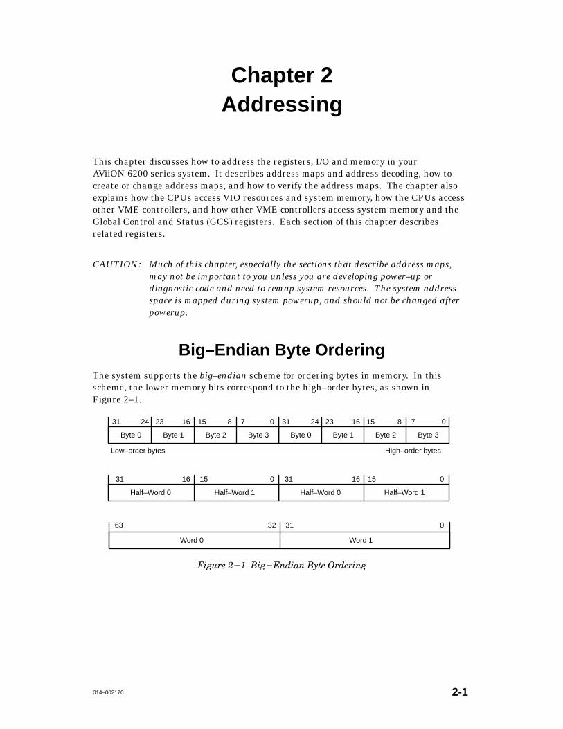
Big–Endian Byte OrderingThe system supports the big–endian scheme for ordering bytes in memory. In thisscheme, the lower memory bits correspond to the high–order bytes, as shown inFigure 2–1.
Word 0 Word 1
63 32 31 0
31 0
31 0
16 15
16 15 8 724 23
Half–Word 1Half–Word 0
Byte 0 Byte 1 Byte 2 Byte 3
31 016 15
Half–Word 1Half–Word 0
31 016 15 8 724 23
Byte 0 Byte 1 Byte 2 Byte 3
Low–order bytes High–order bytes
� �������� � ���� � ���� ���� ��
Addressing
014–0021702-2
Memory Maps and Address DecodingThis section discusses how the system address space is mapped to control access tosystem resources.
CAUTION: This section may not be important to you unless you are developingpower–up or diagnostic code and need to remap system resources. Thesystem address space is mapped during system powerup, and should not bechanged after powerup.
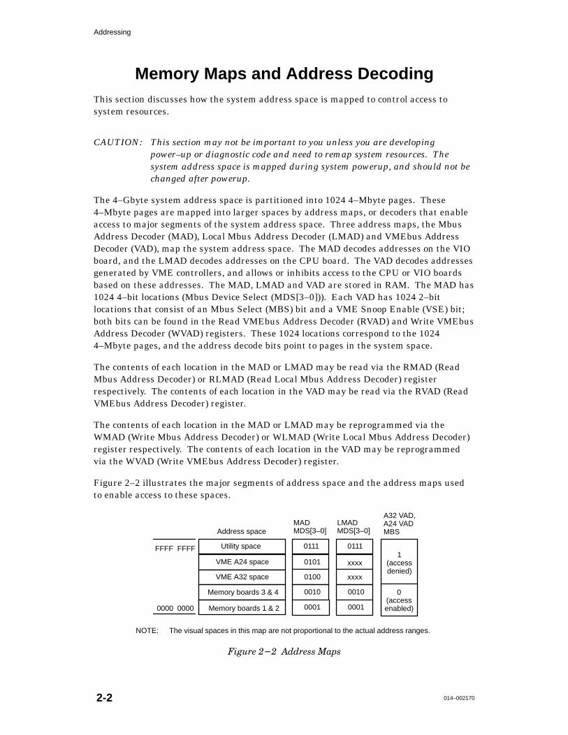
The 4–Gbyte system address space is partitioned into 1024 4–Mbyte pages. These4–Mbyte pages are mapped into larger spaces by address maps, or decoders that enableaccess to major segments of the system address space. Three address maps, the MbusAddress Decoder (MAD), Local Mbus Address Decoder (LMAD) and VMEbus AddressDecoder (VAD), map the system address space. The MAD decodes addresses on the VIOboard, and the LMAD decodes addresses on the CPU board. The VAD decodes addressesgenerated by VME controllers, and allows or inhibits access to the CPU or VIO boardsbased on these addresses. The MAD, LMAD and VAD are stored in RAM. The MAD has1024 4–bit locations (Mbus Device Select (MDS[3–0])). Each VAD has 1024 2–bitlocations that consist of an Mbus Select (MBS) bit and a VME Snoop Enable (VSE) bit;both bits can be found in the Read VMEbus Address Decoder (RVAD) and Write VMEbusAddress Decoder (WVAD) registers. These 1024 locations correspond to the 10244–Mbyte pages, and the address decode bits point to pages in the system space.
The contents of each location in the MAD or LMAD may be read via the RMAD (ReadMbus Address Decoder) or RLMAD (Read Local Mbus Address Decoder) registerrespectively. The contents of each location in the VAD may be read via the RVAD (ReadVMEbus Address Decoder) register.
The contents of each location in the MAD or LMAD may be reprogrammed via theWMAD (Write Mbus Address Decoder) or WLMAD (Write Local Mbus Address Decoder)register respectively. The contents of each location in the VAD may be reprogrammedvia the WVAD (Write VMEbus Address Decoder) register.
Figure 2–2 illustrates the major segments of address space and the address maps usedto enable access to these spaces.
Address space
VME A24 space
VME A32 space
Memory boards 1 & 20000 0000
FFFF FFFF Utility space
NOTE: The visual spaces in this map are not proportional to the actual address ranges.
MADMDS[3–0]
0100
0010
0111
0001
A32 VAD,A24 VADMBS
0(accessenabled)
1(accessdenied)
0101
LMADMDS[3–0]
0010
0111
0001
xxxx
xxxx
Memory boards 3 & 4
��� ���� ��� �� ����

Addressing
014–002170 2-3
The utility space contains the system control registers, including all CMMU registersand VME A16 space.
An A32 VME controller (32 address bits) can access any page in memory, but an A24VME controller (24 address bits) can access only four contiguous pages in memory. TheExtended Address (EXTAD) register defines bits 24–31 for A24 controllers.
The Mbus Address Decoders (LMAD and MAD)Access to system resources is controlled by the LMAD (Local Mbus Address Decoder) andthe MAD (Mbus Address Decoder). The LMAD validates addresses on the CPU board,and the MAD validates addresses on the VIO board.
The LMAD partitions the system address space as follows:
• �����# ����� � ����! ����� �� ��� � ����! ����� ��
• �����# ����� � ����! ����� �� ��� � ����! ����� ��
• ��� ����� �� �!���
• �! ����� ��� ��"���� ����� �
The MAD partitions the system address space as follows:
• �����# ����� � ����! ����� �� ��� � ����! ����� ��
• �����# ����� � ����! ����� �� ��� � ����! ����� ��
• ��� ����� �� �!��� ��� �� �
• �� ��
• �� ��
• �! ����� ��� ��"���� ����� �
Loading and Verifying the LMAD
The Data General power–up code automatically loads and verifies the LMAD while thesystem powers up. The LMAD should not be changed after powerup. If you aredeveloping power–up code or diagnostics and you must rewrite the LMAD, load andverify the LMAD as follows:
1. Clear bit 4 (Mbus Address Decoder Valid (MADV)) of the JPDIAG (Job ProcessorDiagnostic) register to 0 as follows:
A. Read the JPDIAG register (see Chapter 4).
B. Clear bit 4 to 0. Do not change any other bits; these are reserved for DataGeneral use only, and may affect the operation of your system.
C. Write the new value back to JPDIAG.

Addressing
014–0021702-4
2. Write the decode value(s) to the LMAD. The following code example writes to arange of pages in the LMAD.
; r2 = loop count for number of pages to initialize; r3 = MDS (Mbus Device Select) value (see the LWMAD register description); r4 = MPN (Mbus page number), value 0–1023; r5 = page size; r6 = base address for LWMAD register (0xFFC8); Note: 0x indicates a hexadecimal number.
;initialize registersor.u r5,r0,0x0040 ;page size (4MB)mul r4,r4,r5 ;form the MPN (Mbus page number)or.u r6,r0,0xFFC8 ;write LWMAD high address bits to r6bsr init_LMAD ;execute the init_LMAD subroutine
init_LMAD ;loads a single MDS into a range of pagesst r3,r6,0x8020 ;write MDS to LWMAD registerst r3,r4,r0 ;write MDS to the MPN; CAUTION: Do not place any instructions between the store instructions! The; write to MPN must immediately follow the write to LWMAD!addu r4,r4,r5 ;increment to the next pagesubu r2,r2,1 ;decrement the loop counterbcnd ne0,r2,init_LMAD ;loop until 0
3. Verify the decode value in LMAD as follows:
A. Read an MDS value from a location in the LMAD as :
; r3 = MDS (Mbus Device Select) value (see the LWMAD register description); r4 = MPN (Mbus page number), value 0–1023; r6 = base address for LWMAD register (0xFFC8); Note: 0x indicates a hexadecimal number.
ld r3,r6,0x8020 ;load the LRMAD registerld r3,r4,r0 ;load the MDS from the MPN to r3; CAUTION: Do not place any instructions between the load instructions! The; load from MPN must immediately follow the load from LWMAD!
B. Verify the MDS data as desired. You may want to build the above sample into aloop which verifies or writes to a table.
4. Repeat steps 2 and 3 for all locations to be written.
5. Set the MADV bit of the JPDIAG register to 1 as follows:
A. Read the JPDIAG register.
B. Set bit 4 to 1. Do not change any other bits; these are reserved for Data Generaluse only, and may affect the operation of your system.
C. Write the new value back to JPDIAG.

Addressing
014–002170 2-5
Loading and Verifying the MAD
The Data General power–up code automatically loads and verifies the MAD while thesystem powers up. The MAD should not be changed after powerup. If you aredeveloping power–up code or diagnostics that require resetting the MAD, load and verifythe MAD as follows:
1. Clear bit 4 (Mbus Address Decoder Valid (MADV)) of the JPDIAG (Job ProcessorDiagnostic) register to 0 as follows: (this turns off the LMAD)
A. Read the JPDIAG register (see Chapter 4).
B. Clear bit 4 to 0. Do not change any other bits; these are reserved for DataGeneral use only, and may affect the operation of your system.
C. Write the new value back to JPDIAG.
2. Clear bit 1 (Mbus Address Decoder Valid (MDV)) of the CPU Control and Status(CCS) register to 0 as follows: (this turns off the MAD)
A. Read the CCS register (see Chapter 4).
B. Clear bit 1 to 0. Do not change any other bits; these are reserved for DataGeneral use only, and may affect the operation of your system.
C. Write the new value back to CCS.
3. Write the location pointer and decode value to the Write Mbus Address Decoder(WMAD) register.
The data you write into WMAD includes ten bits to select one of the 1024 locationsin the MAD, and four bits to store in that location.
4. Verify the decode value in the MAD as follows:
A. Write the page number into the Mbus Page Number (MPN) bits in the ReadMbus Address Decoder (RMAD) register.
B. Read RMAD. The Mbus Device Select (MDS) bits contain the decode value.
5. Repeat steps 3 and 4 for all locations to be written.
6. Set the MDV bit of the CCS register to 1 as follows: (this turns on the MAD)
A. Read the CCS register (see Chapter 4).
B. Set bit 1 to 1. Do not change any other bits; these are reserved for Data Generaluse only, and may affect the operation of your system.
C. Write the new value back to CCS.
7. Set the MADV bit of the JPDIAG register to 1 as follows: (this turns on the LMAD)
A. Read the JPDIAG register.
B. Set bit 4 to 1. Do not change any other bits; these are reserved for Data Generaluse only, and may affect the operation of your system.
C. Write the new value back to JPDIAG.

Addressing
014–0021702-6
When the MDV or MADV bit of the CCS or JPDIAG register is cleared to zero, the MADor LMAD is turned off. In this state, the upper ten address bits are ignored and alladdresses point into the 4–Mbyte utility space, which includes the powerup PROM andthe VIO board registers. When MDV or MADV is cleared, the utility space begins ataddress 0000 000016. When the MDV or MADV is set to 1, the MAD or LMAD is turnedon. This is the normal operating state where the upper ten address bits are decoded bythe MAD or LMAD and point to the system address space. When MDV or MADV is set,the utility space is mapped to FFC0 000016.
The following pages describe the LRMAD, LWMAD, RMAD and WMAD registers.
LRMAD Read Local Mbus Address Decoder
FFC8 8024 Read only
The Read Local Mbus Address Decoder (LWMAD) register verifies an address decodevalue in the local Mbus address decoder. This operation can only be done by processor 0on each CPU board; processor 1 generates undefined results.
NOTE: LRMAD can be accessed by CPU0, CPU2. CPU4 and CPU6 only.
Resets do not affect LRMAD.
31 16
15 034
Unused MDS
Unused
Bit Mnemonic Function
��� ��$"��
��� ��� ��$" ��%��� �����#
���� ���� ���� ���� ��%��� �����#��
� � � � ����!& �� �� ��� ��
� � � � ����!& �� �� ��� ��
� � � � �#���#& � ���
� � � � �$" !!�!
��� ��%���� ���!�""�" !��$�� �$" �!!�!"�

Addressing
014–002170 2-7
LWMAD Write Local Mbus Address Decoder
FFC8 8020 Write only
The Write Local Mbus Address Decoder (LWMAD) register loads an address decodevalue into the local Mbus address decoder. This operation can only be done by JP0 (jobprocessor 0) on each CPU board; JP1 generates undefined results.
NOTE: LWMAD can be accessed by JP0 (CPU0, CPU2. CPU4 and CPU6) only.
Resets do not affect LWMAD.
31 16
15 034
Unused MDS
Unused
Bit Mnemonic Function
��� ��$"��
��� ��� ��$" ��%��� �����#
���� ���� ���� ���� ��%��� �����#��
� � � � ����!& �� �� ��� ��
� � � � ����!& �� �� ��� ��
� � � � �#���#& � ���
� � � � �$" !!�!
��� ��%���� ���!�""�" !��$�� �$" �!!�!"�

Addressing
014–0021702-8
RMAD Read Mbus Address Decoder
FFF8 8024 Read/Write
Read Mbus Address Decoder (RMAD) verifies the configuration of the Mbus physicaladdress map.
Resets do not affect RMAD.
31 16
15 034
Unused MDS
UnusedMPN
22 21
Bit Mnemonic Function
�� ��� � 0. ��%# �0) #- �+*# +$ �� ,�%#.� ,�%# .'4#�� � 3/#.�
�#�"�2-'/#�
�-'/# �&# 0. )�./#- 2-'/#. /&# *0) #- +$ /&# ��� ,�%# /+ # 1#-'$'#" '*
/&# ��� '/.�
�#�" ��� -#/0-*. /&# ,�%# *0) #- $+- /&# � 0. �#1'!# �#(#!/ ����� !+"#
-#/0-*#"�
�� �*0.#"
��� ��� � 0. �#1'!# �#(#!/
�#�" +*(3�
��� -#/0-*. /&# "#1'!# .#(#!/ 1�(0# $+- /&# ,�%# "#$'*#" 3 ����
���� ��� ��� ���� �#1'!# �#(#!/#"
� � � �#)+-3 � �� �*" �
� � � �#)+-3 � �� �*" �
� � � ��� �� �,�!#
� � ��� �� �,�!#
� �/'('/3 �,�!#
� � �0. �--+-
���� �*1�('" �""-#..#. ,-+"0!# 0. #--+-.�

Addressing
014–002170 2-9
WMAD Write Mbus Address Decoder
FFF8 8020 Write only
Write Mbus Address Decoder (WMAD) is used to load an address decode value into theMbus address decoder.
Resets do not affect WMAD.
31 16
15 034
Unused MDS
UnusedMPN
22 21
Bit Mnemonic Function
�� �������� ��/- ��$" �/(�", �*)" *# ��� +�$"-�
�%" �/- (�-.", 1,&."- .%" )/(�", *# .%" +�$" .* �" (�++"! &) ����
��� �)/-"!
�� ������� ��/- �"0& " �"'" .
�%" �/- (�-.", 1,&."- .%" ��/- !"0& " -"'" . 0�'/" &) ���� �%" ��� 0�'/"-
�," �- #*''*1-
��� ��� ���� ���� �"0& " �"'" ."!
� � � � �"(*,2 �� �� �)! ��
� � � � �"(*,2 � �� �)! ��
� � � � ��� � �+� "
� � � � ��� �� �+� "
� � � � �.&'&.2 �+� "
� � � � �/- �,,*,
���� �)0�'&! �!!,"--"- +,*!/ " �/- ",,*,-�

Addressing
014–0021702-10
The VMEbus Address Decoder (VAD)VME controllers access memory through the VAD.
Loading and Verifying the VAD
The Data General power–up code automatically loads and verifies the VAD while thesystem powers up. The VAD should not be changed after powerup. If you are developingpower–up code or diagnostics that require resetting the VAD, load and verify the VAD asfollows:
1. Clear bit 0 (VMEbus Address Decoder Valid (VDV)) of the CPU Control and Status(CCS) register to 0 (see Chapter 4).
A. Read the CCS register (see Chapter 4).
B. Clear bit 0 to 0. Do not change any other bits; these are reserved for DataGeneral use only, and may affect the operation of your system.
C. Write the new value back to CCS.
2. Write the VMEbus Address Decoder address and decode parameter to the WriteVMEbus Address Decoder (WVAD) register.
The data you write into WVAD includes one bit to select the VAD (A24 VAD or A32VAD), ten bits to select one of the 1024 locations in the VAD, and two bits to storethe decode value in the selected location.
3. Verify the decode value in the VAD as follows:
A. Write the page number into the VPN bits in the RVAD register.
B. Read the RVAD register. The Mbus Select (MBS) bit defines whether or notVME controllers can access the Mbus at this page.
4. Repeat step 2 for all locations to be loaded.
5. Set the VDV bit of the CCS register to 1.
A. Read the CCS register (see Chapter 4).
B. Set bit 0 to 1. Do not change any other bits; these are reserved for Data Generaluse only, and may affect the operation of your system.
C. Write the new value back to CCS.
When the VDV bit of the CCS register is cleared to zero, the VAD is turned off. In thisstate, the VME controllers cannot access the VIO board resources and memory. Whenthe VDV bit of the CCS register is set to 1, the VAD is turned on. This is the normaloperating state where the upper ten address bits are decoded by the VAD and point to apredefined range in the system address space.
Addressing
014–002170 2-11
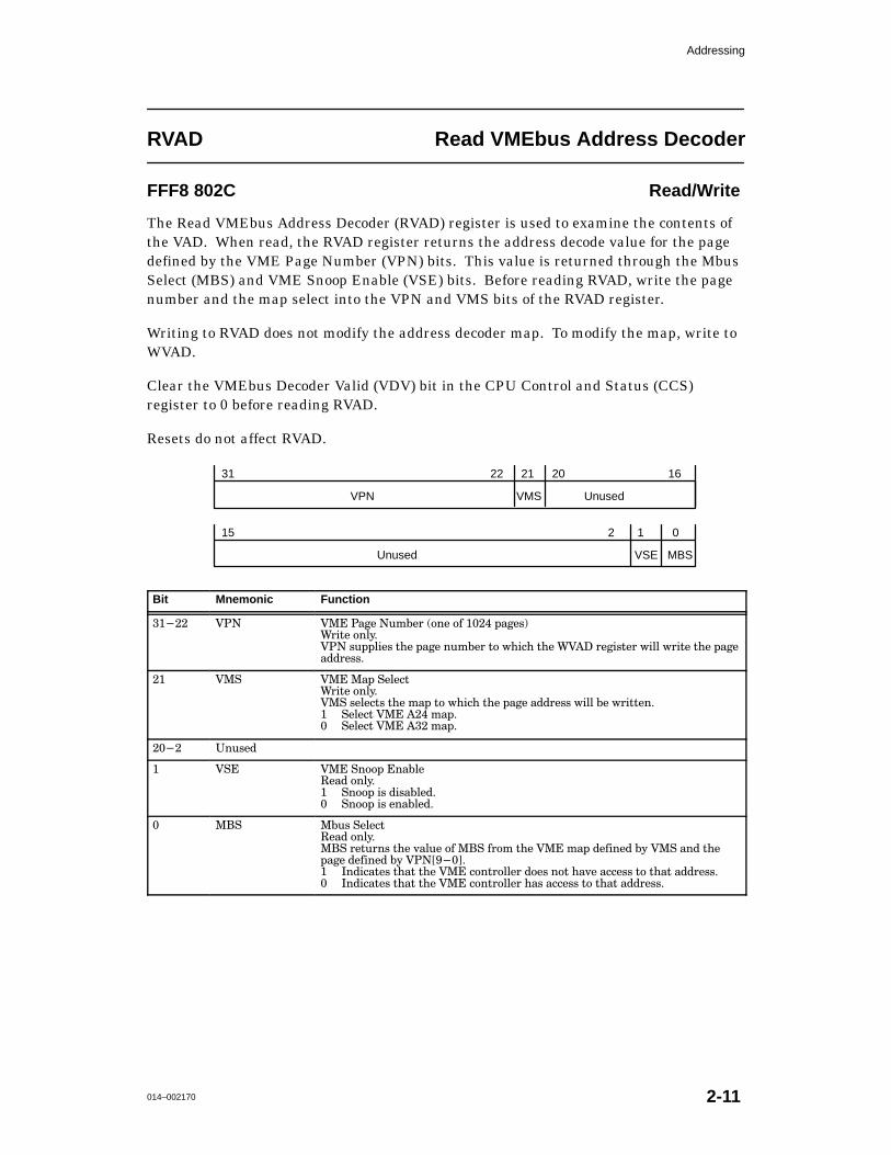
RVAD Read VMEbus Address Decoder
FFF8 802C Read/Write
The Read VMEbus Address Decoder (RVAD) register is used to examine the contents ofthe VAD. When read, the RVAD register returns the address decode value for the pagedefined by the VME Page Number (VPN) bits. This value is returned through the MbusSelect (MBS) and VME Snoop Enable (VSE) bits. Before reading RVAD, write the pagenumber and the map select into the VPN and VMS bits of the RVAD register.
Writing to RVAD does not modify the address decoder map. To modify the map, write toWVAD.
Clear the VMEbus Decoder Valid (VDV) bit in the CPU Control and Status (CCS)register to 0 before reading RVAD.
Resets do not affect RVAD.
Unused
31 22 21 1620
15 012
VPN UnusedVMS
VSE MBS
Bit Mnemonic Function
���� ��� ��� ��!� �,%��) �'&� ' ��� (�!�*�
�)#+� '&$/�
��� *,(($#�* +"� (�!� &,%��) +' ."#�" +"� ���� )�!#*+�) .#$$ .)#+� +"� (�!�
���)�**�
�� ��� ��� ��( ��$��+
�)#+� '&$/�
��� *�$��+* +"� %�( +' ."#�" +"� (�!� ���)�** .#$$ �� .)#++�&�
� ��$��+ ��� �� %�(�
� ��$��+ ��� �� %�(�
���� �&,*��
� ��� ��� �&''( �&��$�
���� '&$/�
� �&''( #* �#*��$���
� �&''( #* �&��$���
� � � ��,* ��$��+
���� '&$/�
� � )�+,)&* +"� -�$,� ' � � )'% +"� ��� %�( �� #&�� �/ ��� �&� +"�
(�!� �� #&�� �/ ���������
� �&�#��+�* +"�+ +"� ��� �'&+)'$$�) �'�* &'+ "�-� ����** +' +"�+ ���)�**�
� �&�#��+�* +"�+ +"� ��� �'&+)'$$�) "�* ����** +' +"�+ ���)�**�

Addressing
014–0021702-12
WVAD Write VMEbus Address Decoder
FFF8 8028 Write Only
Write VMEbus Address Decoder (WVAD) loads the VMEbus address decoders. TheVMEbus has two decoders: one for the A24 address space and one for the A32 addressspace.
Clear the VMEbus Decoder Valid (VDV) bit in the CPU Control and Status (CCS)register to 0 before writing to WVAD.
������ �)"+"% +& �� ."## �!�% � +!� '� � ���)�** +!�+ �� ����**�*� �����
.)"+� +& �� ��+.��% .)"+"% +& �%� )���"% �)&$ �� �
Resets do not affect WVAD.
Unused
31 22 21 1620
15 012
VPN UnusedVMS
VSE MBS
Bit Mnemonic Function
����� ��� ��� �� � �,$��)
��"%�* +!� '� � %,$��) ."+!"% +!� ��� ���)�** ���&��)� �!� �&%+�%+* &�
��� �%� ��� �)� .)"++�% "%+& +!� �'')&')"�+� � �+ +!"* '� � %,$��)�
�� ��� ��� ��' ��#��+
��#��+* +!� ��� ���)�** ���&��) +& �� .)"++�% +&�
� ��#��+* +!� ��� �� $�'�
� ��#��+* +!� ��� �� $�'�
���� �%,*��
� ��� ��� �%&&' �%��#�
��(,�*+* +!� $�*+�) ���� +& *%&&' +!� ����,* �&) � -�#"� ��,* ���)�**�
� �%&&' "* �"*��#���
� �%&&' "* �%��#���
� ��� ��,* ��#��+
��"%�* .!�+!�) +!� ����,* !�* ����** +& +!� ��,* �+ +!� '� � %,$��)
���"%�� �/ +!� ��� �"+*�
� �)�-�%+* ��� ����** +& +!� ��,* �+ +!�+ '� � %,$��)�
� ##&.* ��� ����** +& +!� ��,* �+ +!�+ '� � %,$��)�
Addressing
014–002170 2-13
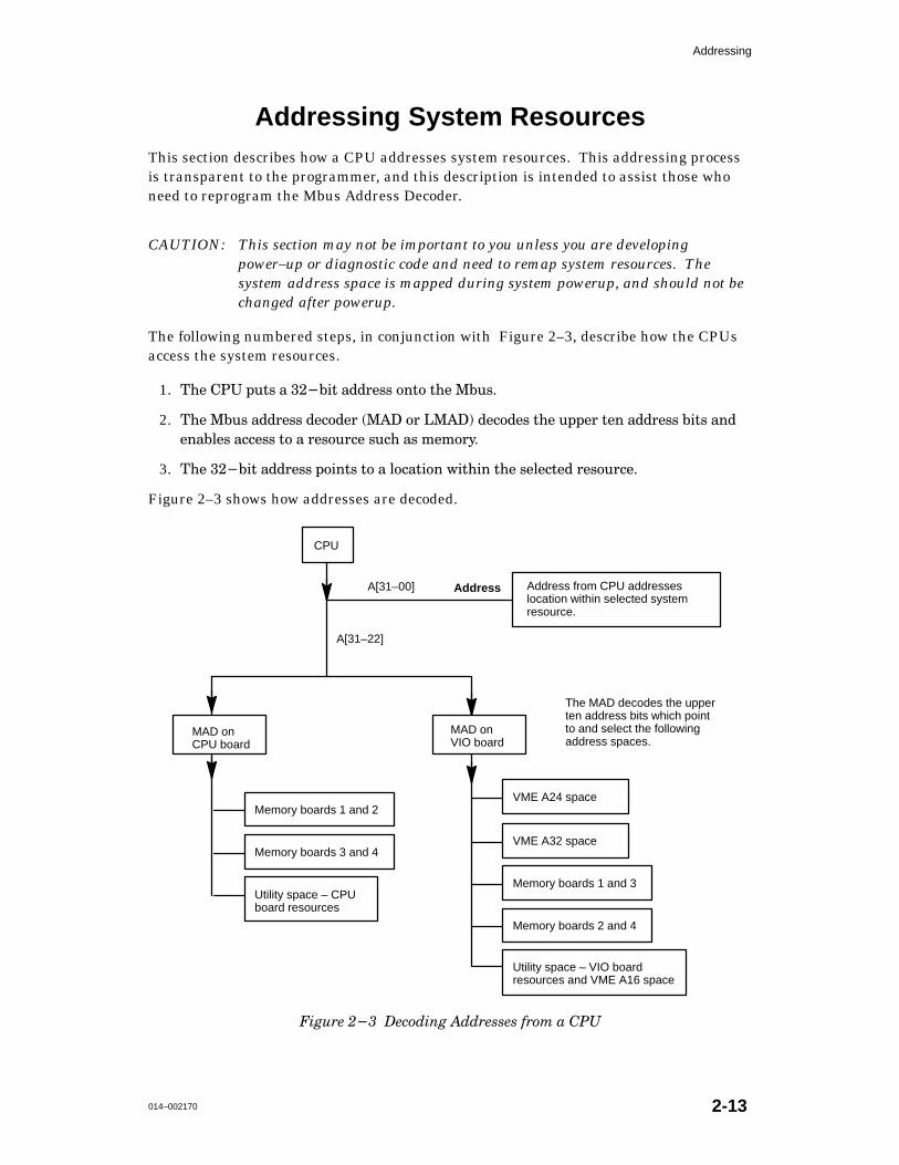
Addressing System ResourcesThis section describes how a CPU addresses system resources. This addressing processis transparent to the programmer, and this description is intended to assist those whoneed to reprogram the Mbus Address Decoder.
CAUTION: This section may not be important to you unless you are developingpower–up or diagnostic code and need to remap system resources. Thesystem address space is mapped during system powerup, and should not bechanged after powerup.
The following numbered steps, in conjunction with Figure 2–3, describe how the CPUsaccess the system resources.
1. ��� � ���� � ������ ������� ���� ��� �����
2. ��� ���� ������� ������� ��� �� ���� ������� ��� ����� ��� ������� ���� ���������� ������ �� � �������� ���� �� �����!�
3. ��� ������ ������� ������ �� � �������� ����� ��� �������� ���������
Figure 2–3 shows how addresses are decoded.
CPU
MAD onCPU board
Address from CPU addresseslocation within selected systemresource.
Memory boards 1 and 2
Memory boards 3 and 4
VME A24 space
VME A32 space
Utility space – CPUboard resources
A[31–00]
A[31–22]
The MAD decodes the upperten address bits which pointto and select the followingaddress spaces.
Address
MAD onVIO board
Utility space – VIO boardresources and VME A16 space
Memory boards 1 and 3
Memory boards 2 and 4
���������� ���� ��� � ������ ���� � �

Addressing
014–0021702-14
Addressing a VME ControllerThis section describes how to address VME controllers. This addressing process istransparent to the programmer, and much of this description is intended to assist thosewho need to reprogram the Mbus Address Decoders.
Construct addresses to A16, A24 or A32 VME controllers as follows:
A16 = FFFF nnnn ����� nnnn �� ��� ���� ������ ��� �������� �� �� ���
A24 = FEnn nnnn ����� nn nnnn �� ��� ���� ������ ��� �������� �� �� ���
A32 = nnnn nnnn ����� nnnn nnnn �� ��� ���� ������ ��� ������ �� �� ���
Figure 2–4 illustrates how the VMEbus decodes addresses, and where the addressmodifier bits come from.
Mbus address bits MDS[2–0] bits of RMADregister are translated intoAM[5–4] bits.
VMEbus address modifierbits AM[5–4]
VMEbus address bits
EXTAM register bits:EXTAM[3–0]
VMEbus address Type of VMEbus accessVME address space select:A16, A24 or A32
VMEbus address modifierbits AM[3–0]
VMEbus
AM[3–0] AM[5–4]A[31:01] (A32)A[23:01] (A24)A[15:01] (A16)
���������� ���� ��� � ������ �� ��� ����
The MDS[3–0] bits, derived from the address, are translated into the address modifierbits AM[5–4]. The address modifier bits inform the VME controllers which VME spacethe address is written to: A16, A24 or A32 space. See Table 2–1 and Table 2–2 in thedescription of the EXTAM register that follows for more information about the addressmodifier bits.

Addressing
014–002170 2-15
EXTAM Extended Address Modifier
FFF8 8014 Read/write
The extended address–modifier register (EXTAM) supplies the address modifier bitsAM[3–0] to the VMEbus when a CPU accesses the VMEbus. The address modifier bitsAM[5–0] supply the VME devices with information such as address size, type of access,and identification of the bus master. Address modifier bits AM[5–4] identify the VMEaddress space, and are decoded (by logic) from MDS[2–0] as shown below. AM[5–4] isput on the VMEbus. Table 2–1 illustrates how the address modifier bits (AM[5–4]) arederived from the Mbus device select bits (MDS[2–0]) found in the RMAD register.
Table 2–1 Address Modifier Translation Table
VME space MDS2 MDS1 MDS0 AM5 AM4
� � � � � �
�� � � � � �
��� � � � � �
The address modifier defines the type of transfer or access, and is driven onto theVMEbus with each address. Table 2–2 defines the address modifier bits.
Table 2–2 Address Modifiers (Transfer Type)
AM3 AM2 AM1 AM0 Type of access
� � � � �/+!,0%-*, �'*�& .,�)-"!,
� � � � �/+!,0%-*, +,*#,�( ���!--
� � � � �/+!,0%-*, �.� ���!--
� � � � �-!, �'*�& .,�)-"!,
� � � � �-!, +,*#,�( ���!--
� � � � �-!, �.� ���!--
����� � /-!, .,�)-"!, *, /-!, ���!-- %- .$! -�(! �- � )*)�+,%0!'!#! ���!-- !"%)! %) .$!
����/- -+!�%"%��.%*)�
Initialize EXTAM before addressing a VME controller.
Resets do not affect EXTAM.
EAM
7 034
Unused
Bit Mnemonic Function
�� �)/-!
�� ��� �2.!) ! � ,!-- �* %"%!,-
�,%0!- .$! � ,!-- (* %"%!,- ������ *).* .$! ����/- 1$!) � ��� 1,%.!-
�) � ,!-- .* .$! ����/-� �$! � ,!-- (* %"%!, !"%)!- .$! .3+! *" .,�)-"!,
*, ���!-- �-!! ���'!��� � ,!-- �* %"%!,-��

Addressing
014–0021702-16
Addressing System Memory and Registersfrom a VME Controller
This section describes how VME controllers address system memory and registers. Thisaddressing process is transparent to the programmer, and this description is intended toassist those who need to reprogram the Mbus Address Decoder. The following text andillustrations explain how the CPUs access the system resources.
CAUTION: This section may not be important to you unless you are developingpower–up or diagnostic code and need to remap system resources. Thesystem address space is mapped during system powerup, and should not bechanged after powerup.
VME controllers have one of three address spaces: A16, A24 or A32 space, and arerespectively referred to as A16, A24 or A32 controllers. The number of address linesdriven by the controller defines the address space or range available.
A16 controllers %�1" �� �!!-".. (&*".� ��� +*/-+(("-. �* � ".. +*(4 /%" �(+��(
�+*/-+( �*! �/�/0. ����� -"$&./"-. �*! +/%"- ��� +*/-+(("-.�
A24 controllers %�1" � �!!-".. (&*".� �� +*/-+(("-. �* � ".. �..&$*"! .4./")
)")+-4 +*(4 �#/"- /%" ��� %�. &*./-0 /"! /%") /+ !+ .+� �%"* �*
�� +*/-+(("- � "..". .4./") )")+-4� /%" ����� -"$&./"- �,,"*!.
/%" 0,,"- "&$%/ �!!-".. �&/. /+ /%" �� �!!-"..� �%&. "*��(". /%" ��
!"1& " /+ �!!-".. /%" +--" / ,�$". &* )")+-4� �%"* �!!-"..&*$
.4./") )")+-4� /%" �!!-".. )+!&#&"- �&/. ������ !"#&*" /%" /4," +#
� ".. 2%"/%"- /%" /-�*.#"- &. /+ 0."- .,� " +- /+ .0,"-1&.+- .,� "� �*!
2%"/%"- /%"." � "..". �-" �(+ '� ,-+$-�) +- !�/� � "..".�
A32 controllers %�1" �!!-".. (&*".� /%"-"#+-" /%"&- �!!-"..&*$ -�*$" "3/"*!.
/%-+0$%+0/ /%" � �� .4./") �!!-".. .,� "� � +*/-+(("-. �* � "..
�..&$*"! .4./") )")+-4 �*! /%" ��� -"$&./"-. �. 2"(( �. +/%"- ���
+*/-+(("-.�
The VME Address Decoders (VAD) process addresses from VME controllers, and if theseaddresses decode addresses from VME controllers. There are two VADs: one torepresent A24 controllers called the A24 VAD, and one for the A32 controllers called theA32 VAD. When a VME controller addresses a system board resource or a location insystem memory that it has access to, the appropriate VAD enables access to the location.If the address points to space that is not allocated to the VME controllers, the VAD willnot allow access to the resource. This restriction prevents VME controllers fromaccessing system resources that are not assigned for use by VME controllers.
The GRPAD[7–0] and BDAD[3–0] DIP switches define the base address of the GCSregisters.
Figure 2–5 illustrates how VME controllers address system board resources and systemmemory.

Addressing
014–002170 2-17
The VME interface appends the EXTAD bits 31–24to the VME address bits 23–00. The EXTAD bitsconvert the A24 address into a 32–bit address.
VME controller asserts anaddress on the VMEbus.
A24 or A32address?
A24 address
The VME interface puts the 32–bitaddress generated by the VME controlleronto the Mbus.
If the address is to A32 space, bits 31–22 flow through VAD to allow ordeny access to the VIO board. If the address is to A24 space, bits23–22 flow through VAD to allow or deny access to the VIO board.
Access toVIO boardallowed?
Yes
No Decodes to another VMEcontroller or produces a buserror.
The MAD and LMAD processes the addressbits A[31–22] and select the resource.
A32 address
A24 or A32VME controller Master
Address
AddressA[31–0]
VAD
System board select
MAD orLMAD
Resource selectSlaveResource *
* The resource is:memory boards 1 & 2memory boards 3 & 4VIO board resource
VMEbus Interface
Address
���������� ���������� ������ �������� ���� �� ����������

Addressing
014–0021702-18
The EXTAD register, whose definition follows, is appended to addresses from A24 VMEcontrollers to generate 32-bit addresses for the Mbus.
EXTAD Extended Address
FFF8 8010 Read/write
The extended address register provides the upper 8 Mbus address bits when an A24VMEbus device accesses the Mbus. EXTAD is loaded during powerup with a baseaddress for VME access to system memory.
Resets do not affect EXTAD.
EXT
7 0
Bit Mnemonic Function
�� ��� �&"����� �� �!!
�#�����! "�� ��� �!! ��"! ������� "� "�� �#! %��� �� �� � ��#! ��$���
����!!�! "�� �#!�
24–bit address
15 0
1631 24 23
EXTAD 24–bit address
A VME A24 Address to System Memory
A VME A32 Address to System Memory
31
Address within 4–Mbyte page
22 21 16
15 0
Address of 4–Mbyte page Address within 4–Mbyte page
���������� �������� �� � ������ ���� �� ����������� �� ����� �����
��� �� ����"�

014–002170 3-1
Chapter 3Interrupts
Interrupts are a means for the system resources to notify a CPU of a condition thatneeds attention. Each interrupt has an associated interrupt service routine that theCPU executes.
This chapter discusses interrupts, how the interrupting devices interrupt the CPU, andhow the CPU handles the interrupts.
CPU Interrupt RegistersThis section describes the registers used to interrupt the CPUs and pass interruptinformation.
The VIO board has the following registers:
CLRINT Clear InterruptCLRSWI Clear Software InterruptsIEN Interrupt EnableISS Interrupt Source StatusIST Interrupt StatusSETSWI Set Software Interrupts
Each CPU board has the following registers:
ABTCLR Clear Abort InterruptJPIEN Job Processor Interrupt EnableJPIST Job Processor Interrupt StatusXCLR Clear Cross InterruptXSET Set Cross Interrupt
The IST, SETSWI, JPIST and XSET interrupts pass interrupt requests to the CPUs, andsefine which interrupt requests are currently asserted. When your interrupt serviceroutine handles an interrupt, be sure to clear that interrupt.
The CLRINT, CLRSWI, and XCLR registers clear some interrupts. If you need to clearan interrupt, check these registers. If the interrupt appears in one of these registers,write to the register as defined in the register description.
The IEN and JPIEN enable or mask interrupt requests passed through the IST andJPIST registers. To enable or mask an interrupt, write to the appropriate register asdefined in the register descriptions that follow.

Interrupts
014–0021703-2
ABTCLR Clear Abort Interrupt
FFC8 3000 Write only
The Clear Abort Interrupt (ABTCLR) register clears the abort interrupt (bit 1 (ABT) ofthe JPIST register) to 0 when ABTCLR is either read or written.
NOTE: Each CPU board has an ABTCLR register. The currently active job processoruses the ABTCLR register.
31 16
15 0
ABTCLR
ABTCLR
Bit Mnemonic Function
���� ���� ����" � "$ �$�""%!$
����"# $�� �� "$ ��$�""%!$ '��� ��$��" "��� " '"�$$���
����� ���� "���� $�� &��%� "�$%"��� �# %���������
���� '"�$$��� �( � �&��$� � '"�$� � � �&�� $� %�� ��( &��%� '���
' "��

Interrupts
014–002170 3-3
CLRINT Clear Interrupt
FFF8 408C Write Only
The Clear Interrupt (CLRINT) register clears the abort, ac fail, system fail, and printerinterrupts in the IST register. The abort interrupt is generated when the abortpushbutton is pressed. The ac fail interrupt is generated when the power supply assertsthe ACFAIL line on the VMEbus. The system fail interrupt is generated when any VMEcontroller asserts SYSFAIL.
To clear an interrupt request, write a 1 to the appropriate bit in the CLRINT register.For example, to clear a system failure interrupt request, write a 1 into the CSF bit. Thisclears the System Failure (SF) bit in the Interrupt Status (IST) register.
Resets do not affect CLRINT.
0
CSF
1
CAC
2
CAB
3
Unused
15
CPR
4
Bit Mnemonic Function
��� �#*(��
�� � �!��' )�� �' #)�' *���' �� �� �#)�''*%) ��&*�()�
� �!��'( )�� %' #)�' �*���' #)�''*%) '�&*�()�
� ���+�( )�� %' #)�' �*���' #)�''*%) '�&*�() *#���#����
� �� � �!��' )�� ��$') �� �� �#)�''*%) ��&*�() �� ) � $� �����
� �!��'( )�� � �� #)�''*%) '�&*�()�
� ���+�( )�� � �� #)�''*%) '�&*�() *#���#����
� ���� �!��' )�� �� �� ! ����� �#)�''*%) ��&*�() �� ) � $� �����
� �!��'( )�� ��� �%$,�' �� !� #)�''*%) '�&*�()�
� ���+�( )�� ��� �%$,�' �� !� #)�''*%) '�&*�() *#���#����
� ��� �!��' )�� (-()�" �� !*'� ���� �#)�''*%) ��&*�() �� ) �� $� �����
� �!��'( )�� �� #)�''*%) '�&*�()�
� ���+�( )�� �� #)�''*%) '�&*�() *#���#����

Interrupts
014–0021703-4
CLRSWI Clear Software Interrupt
FFF8 4084 Write Only
The Clear Software Interrupt (CLRSWI) register clears software interrupts. To clear asoftware interrupt, set a bit in CLRSWI. This clears the corresponding interrupt in theInterrupt Status (IST) register.
0123
CI7
7 6 5 4
CI6 CI5 CI4 CI1 CI0CI3 CI2Unused
815
Bit Mnemonic Function
�� ����� ���� ��� ���������
� ������ ���� ��� ��������� �
� ����� ���� ��� ��������� ����������
�� ����� ���� ��� ���������
� ������ ���� ��� ��������� �
� ����� ���� ��� ��������� ����������
� ��� ����� ���� ��� ��������� �
� ������ ���� ��� ��������� ��
� ����� ���� ��� ��������� � ����������
� ��� ����� ���� ��� ��������� �
� ������ ���� ��� ��������� ��
� ����� ���� ��� ��������� � ����������
� ��� ����� ���� ��� ��������� �
� ������ ���� ��� ��������� ��
� ����� ���� ��� ��������� � ����������
� ��� ����� ���� ��� ��������� �
� ������ ���� ��� ��������� ��
� ����� ���� ��� ��������� � ����������
� ��� ����� ���� ��� ��������� �
� ������ ���� ��� ��������� ��
� ����� ���� ��� ��������� � ����������
� ��� ����� ���� ��� ��������� �
� ������ ���� ��� ��������� ��
� ����� ���� ��� ��������� � ����������

Interrupts
014–002170 3-5
IEN, IEN0, IEN1, IEN2 and IEN3 Interrupt Enable
FFF8 403C IEN Write Only
FFF8 4004 IEN0
FFF8 4008 IEN1
FFF8 4010 IEN2
FFF8 4020 IEN3
The Interrupt Enable registers (IEN, IEN0 – IEN3) enable and mask interrupts to theCPU boards. IEN0 – IEN3 enable interrupts to the corresponding CPU board (0 – 3),while IEN enables interrupts to all CPU boards. To enable an interrupt, write a 1 intothe corresponding bit in the appropriate interrupt enable register. To mask an interrupt,write a 0 into the corresponding bit in the interrupt enable register. The interruptenable registers and the interrupt status register are mirror images of each other.
The interrupt enable registers are cleared to 0 by system reset and is not affected bylocal reset.
0
31 30 29 28 27 26 25 24 23 22 21 1617181920
15 14 13 12 11 10 9 8 7 6 5 01234
ABT ACF ATO DTI SI7 SI6 SI5 SI4 IR7 CIO SF IR6 DI SHPMEMSBM
0 PBE 0 0IR5 IR4 IR3 LMI SLP IR2 IR1 SI1 SI0SI2SI3
Bit Mnemonic Function
�� ��� ��)+- �.,#�.--)(
� �(��&!, -#! ��)+- *.,#�.--)( $(-!++.*-�
� ��,%, -#! ��)+- *.,#�.--)( $(-!++.*-
�� ��� �� ��$&.+!
� �(��&!, -#! �� *)/!+ "�$&.+! $(-!++.*-�
� ��,%, -#! �� *)/!+ "�$&.+! $(-!++.*-�
� ��� ����., �$'!).-
� �(��&!, -#! ����., -$'!).- $(-!++.*-�
� ��,%, -#! ����., -$'!).- $(-!++.*-�
�� ��� ����� �$'!+
� �(��&!, ����� -$'!+ $(-!++.*-,�
� ��,%, ����� -$'!+ $(-!++.*-,�
�� ��� �)"-/�+! �(-!++.*- �
� �(��&!, ,)"-/�+! $(-!++.*- ��
� ��,%, ,)"-/�+! $(-!++.*- ��
� �� �)"-/�+! �(-!++.*-
� �(��&!, ,)"-/�+! $(-!++.*- �
� ��,%, ,)"-/�+! $(-!++.*- �
� �� �)"-/�+! �(-!++.*-
� �(��&!, ,)"-/�+! $(-!++.*- �
� ��,%, ,)"-/�+! $(-!++.*- �
��)(-$(.! �

Interrupts
014–0021703-6
Bit Mnemonic Function
� �� �-&14!/% �,1%//2.1
� �,!"*%0 0-&14!/% (,1%//2.1 �
� �!0)0 0-&14!/% (,1%//2.1 �
� �� �� �%3%* �,1%//2.1
� �,!"*%0 1'% ��� (,1%//2.1 &/-+ �� #-,1/-**%/0�
� �!0)0 1'% ��� (,1%//2.1 &/-+ �� #-,1/-**%/0�
�� �,20%$
�� ��� ��� �,1%//2.1
� �,!"*%0 1'% ��� (,1%//2.1�
� �!0)0 1'% ��� (,1%//2.1�
�� �� �501%+ �!(*2/% �,1%//2.1
� �,!"*%0 1'% 0501%+ &!(*2/% (,1%//2.1�
� �!0)0 1'% 0501%+ &!(*2/% (,1%//2.1�
�� ��� �� �%3%* � �,1%//2.1
� �,!"*%0 1'% ���� (,1%//2.1 &/-+ �� #-,1/-**%/0�
� �!0)0 1'% ���� (,1%//2.1 &/-+ �� #-,1/-**%/0�
�� ��� �%+-/5 �,1%//2.1
� �,!"*%0 1'% +%+-/5 (,1%//2.1�
� �!0)0 1'% +%+-/5 (,1%//2.1�
� �� ����� �,1%//2.1
� �,!"*%0 1'% ����� (,1%//2.1�
� �!0)0 1'% ����� (,1%//2.1�
��� �� �,20%$
� ��� �� �%3%* � �,1%//2.1
� �,!"*%0 1'% ���� (,1%//2.1 &/-+ �� #-,1/-**%/0�
� �!0)0 1'% ���� (,1%//2.1 &/-+ �� #-,1/-**%/0�
� �,20%$
�� �� �� �%3%* �,1%//2.1
� �,!"*%0 1'% ��� (,1%//2.1 &/-+ �� #-,1/-**%/0�
� �!0)0 1'% ��� (,1%//2.1 &/-+ �� #-,1/-**%/0�
�� ��� �/(,1%/ �2&&%/ �+.15
� �,!"*%0 1'% ./(,1%/ "2&&%/ %+.15 (,1%//2.1�
� �!0)0 1'% ./(,1%/ "2&&%/ %+.15 (,1%//2.1�
�� �� �� �%3%* �,1%//2.1
� �,!"*%0 1'% ��� (,1%//2.1 &/-+ �� #-,1/-**%/0�
� �!0)0 1'% ��� (,1%//2.1 &/-+ �� #-,1/-**%/0�
� �,20%$
� ��� �-#!1(-, �-,(1-/ �,1%//2.1
� �,!"*%0 1'% *-#!1(-, +-,(1-/ (,1%//2.1�
� �!0)0 1'% *-#!1(-, +-,(1-/ (,1%//2.1�
�,20%$
� ��� �� �%3%* � �,1%//2.1
� �,!"*%0 1'% ���� (,1%//2.1 &/-+ �� #-,1/-**%/0�
� �!0)0 1'% ���� (,1%//2.1 &/-+ �� #-,1/-**%/0�
� �,20%$
�#-,1(,2%$�

Interrupts
014–002170 3-7
Bit Mnemonic Function
��� � ��$�� � ��"� #�"
� �����! "�� ���� ��"� #�" � �� � ���" ���� !�
� �!�! "�� ���� ��"� #�" � �� � ���" ���� !�
� ��� ���"%� � ��"� #�" �
� �����! !��"%� � ��"� #�" ��
� �!�! !��"%� � ��"� #�" ��
� ��� ���"%� � ��"� #�" �
� �����! !��"%� � ��"� #�" ��
� �!�! !��"%� � ��"� #�" ��
� ��� ���"%� � ��"� #�" �
� �����! !��"%� � ��"� #�" ��
� �!�! !��"%� � ��"� #�" ��
� ��� ���"%� � ��"� #�" �
� �����! !��"%� � ��"� #�" ��
� �!�! !��"%� � ��"� #�" ��
������#����

Interrupts
014–0021703-8
ISS Interrupt Source Status
FFF8 4088 Read Only
The Interrupt Source Status (ISS) register gives the current status of the printer buffer,abort, ac failure and system failure interrupts.
Resets do not affect ISS.
15 0123
ABT ACF SFUnused
4
PBS
Bit Mnemonic Function
���� �%,*��
��� �)#%+�) �, �) �+�+,*
� �%�#��+�* +"�+ +"� +"� ')#%+�) �, �) #* %&+ ,$$�
� �%�#��+�* +"�+ +"� ')#%+�) �, �) #* ,$$�
�� �&)+ �,++&% �+�+,*
� �%�#��+�* +"�+ +"� ��&)+ *-#+�" #* +&!!$���
� �%�#��+�* +"�+ +"� ��&)+ *-#+�" #* %&+ +&!!$���
� �� �� �� �+�+,*
� �%�#��+�* +"�+ �% �� �#$ #%+�)),'+ )�(,�*+ #* '�%�#%!� #��� +"� �� �� $#%�
&% +"� ����,* #* �**�)+�� �$&-��
� �%�#��+�* +"�+ +"�)� #* %& �� �#$ #%+�)),'+� #��� +"� �� �� $#%� &% +"�
����,* #* %&+ �**�)+�� �"#!"��
� �� ���� �� �+�+,*
� �%�#��+�* +"�+ ���� �� #* �**�)+�� �$&-� &% +"� ����,*�
� �%�#��+�* +"�+ ���� �� #* %&+ �**�)+�� �"#!"� &% +"� ����,*�

Interrupts
014–002170 3-9
IST Interrupt Status
FFF8 4040 Read Only
The Interrupt Status (IST) register contains interrupt flags that are set to 1 by devicesrequesting an interrupt to the CPU. When a device requests an interrupt, the interruptrequest signal goes to interrupt logic which sets the corresponding interrupt bit in theIST register. The interrupt logic also interrupts the CPU. When interrupted, the CPUmust execute a primary interrupt service routine to find out what kind of interrupt it is.The interrupt service routine may read an interrupt enable register as well as theinterrupt status register. If it does read an interrupt enable register, it must comparethe two registers to find any enabled interrupt(s). The bits in the interrupt enableregisters and the interrupt status register are mirror images of each other.
Resets do not affect IST bits; IST can only be cleared using software.
Unused
31 30 29 28 27 26 25 24 23 22 21 1617181920
15 14 13 12 11 10 9 8 7 6 5 01234
ABT ACF ATO DTI SI7 SI6 SI5 SI4 IR7 CIO SF IR6 DI SHPMEMSBM
PBEIR5 IR4 IR3 LMI SLP IR2 IR1 SI1 SI0SI2SI3Unused Unused Unused
Bit Mnemonic Function
� �� �(+- �.,#�.--('
�# () +�-$'" ,2,- & ��' ., -#$, -( $'$-$�- � ,(!-0�+ + , -�
� �'�$��- , -#�- -# ��(+- ,0$-�# 0�, )+ ,, ��
� �'�$��- , -#�- -# ��(+- ,0$-�# 0�, '(- )+ ,, ��
� �� � ��$%.+
� �'�$��- , -#�- �' �� )(0 + !�$%.+ #�, (��.++ �� �# �� !�$%.+ ,$"'�%
(+$"$'�- , !+(& -# )(0 + ,.))%2� 0#$�# $, �('' �- � -( -# ����.,�
� �'�$��- , -#�- -# + #�, '(- � ' �' �� )(0 + !�$%.+ �
�� �� ����., +�$- + �$& �.-
� �'�$��- , -#�- -# ����., �., "+�'- #�, -$& � (.- �'� " ' +�- � �'
$'- ++.)-�
� �'�$��- , -#�- -# ����., �., "+�'- #�, '(- -$& � (.-�
�� ��� �� �� �$& + �'- ++.)- �,2,- & �(',(% �
� �'�$��- , -#�- -# ,2,- & �(',(% �� �� $, + *. ,-$'" �' $'- ++.)-�
� �'�$��- , -#�- -# ,2,- & �(',(% �� �� $, '(- + *. ,-$'" �' $'- ++.)-�
� �� �(!-0�+ �'- ++.)-
�' (! ,$1 ,(!-0�+ $'- ++.)-,� �# $'- ++.)- , +/$� +(.-$' � !$' , -# ��'
)+$(+$-2 % / %,�
� �'�$��- , -#�- � ,(!-0�+ $'- ++.)- 0�, " ' +�- ��
� �'�$��- , -#�- � ,(!-0�+ $'- ++.)- 0�, '(- " ' +�- ��
��('-$'. ��

Interrupts
014–0021703-10
Bit Mnemonic Function
�� �-&25!0% �,2%003.2
�,% -& 1)6 1-&25!0% ),2%003.21� �(% ),2%003.2 1%04)#% 0-32),% $%&),%1 2(% ��,
.0)-0)27 *%4%*1�
� �,$)#!2%1 2(!2 ! 1-&25!0% ),2%003.2 5!1 '%,%0!2%$�
� �,$)#!2%1 2(!2 ! 1-&25!0% ),2%003.2 5!1 ,-2 '%,%0!2%$�
� ��� �-&25!0% �,2%003.2 �
�,% -& 1)6 1-&25!0% ),2%003.21� �(% ),2%003.2 1%04)#% 0-32),% $%&),%1 2(% ��,
.0)-0)27 *%4%*1�
� �,$)#!2%1 2(!2 ! 1-&25!0% ),2%003.2 5!1 '%,%0!2%$�
� �,$)#!2%1 2(!2 ! 1-&25!0% ),2%003.2 5!1 ,-2 '%,%0!2%$�
� ��� �-&25!0% �,2%003.2 �
�,% -& 1)6 1-&25!0% ),2%003.21� �(% ),2%003.2 1%04)#% 0-32),% $%&),%1 2(% ��,
.0)-0)27 *%4%*1�
� �,$)#!2%1 2(!2 ! 1-&25!0% ),2%003.2 5!1 '%,%0!2%$�
� �,$)#!2%1 2(!2 ! 1-&25!0% ),2%003.2 5!1 ,-2 '%,%0!2%$�
��� ��� �%4%* � �,2%003.2
� *%4%* � ),2%003.2 ����� -, 2(% ���"31� )1 -,% -& 1%4%, .-11)"*% ),2%003.2
0%/3%121 &0-+ ��� #-,20-**%01� ���� (!1 2(% ()'(%12 .0)-0)27 !,$ ���� (!1
2(% *-5%12 .0)-0)27�
� �,$)#!2%1 2(!2 ����� -, 2(% ���"31� )1 !11%02%$�
� �,$)#!2%1 2(!2 ����� -, 2(% ���"31� )1 ,-2 !11%02%$�
�,31%$
� ��� ��� �,2%003.2
� �,$)#!2%1 2(!2 2(% ��� 0%/3%12%$ !, ),2%003.2�
� �,$)#!2%1 2(!2 2(% ��� $)$ ,-2 0%/3%12 !, ),2%003.2�
� �� �712%+ �!)*30% �,2%003.2
� �,$)#!2%1 2(!2 2(% 1712%+ &!)*30% �� ������ *),% -, 2(% ���"31 5!1
!11%02%$� � 1712%+ &!)*30% -##300%$�
� �,$)#!2%1 2(!2 2(% 1712%+ &!)*30% �� ������ *),% -, 2(% ���"31 5!1 ,-2
!11%02%$� �(%0% (!1 ,-2 "%%, ! 1712%+ &!)*30%�
�� �� ��� �%4%* �,2%003.2
� *%4%* ),2%003.2 ���� � -, 2(% ���"31� )1 -,% -& 1%4%, .-11)"*% ),2%003.2
0%/3%121 &0-+ ��� #-,20-**%01� ����� (!1 2(% ()'(%12 .0)-0)27 !,$ ����� (!1
2(% *-5%12 .0)-0)27�
� �,$)#!2%1 2(!2 ��� �� -, 2(% ���"31� )1 !11%02%$�
� �,$)#!2%1 2(!2 ��� �� -, 2(% ���"31� )1 ,-2 !11%02%$�
�� ��� �%+-07 �,2%003.2
��� $%&),%1 5(%2(%0 -0 ,-2 !, ��� %00-0 (!1 -##30%$�
� �,$)#!2%1 2(!2 ! +%+-07 %00-0 (!1 -##300%$�
� �,$)#!2%1 2(!2 ! +%+-07 %00-0 (!1 ,-2 -##300%$�
�� �� ����� �,2%003.2
� �,$)#!2%1 2(!2 2(% ����� )1 0%/3%12),' !, ),2%003.2�
� �,$)#!2%1 2(!2 2(% ����� )1 ,-2 0%/3%12),' !, ),2%003.2�
� � �� �,31%$
�� ��� ��� �%4%* � �,2%003.2
� *%4%* � ),2%003.2 ������ -, 2(% ���"31� )1 -,% -& 1%4%, .-11)"*% ),2%003.2
0%/3%121 &0-+ ��� #-,20-**%01� ����� (!1 2(% ()'(%12 .0)-0)27 !,$ ����� (!1
2(% *-5%12 .0)-0)27�
� �,$)#!2%1 2(!2 ������ -, 2(% ���"31� )1 !11%02%$�
� �,$)#!2%1 2(!2 ������ -, 2(% ���"31� )1 ,-2 !11%02%$�
� �,31%$
� ��� ��� �%4%* � �,2%003.2
� *%4%* � ),2%003.2 ������ -, 2(% ���"31� )1 -,% -& 1%4%, .-11)"*% ),2%003.2
0%/3%121 &0-+ ��� #-,20-**%01� ����� (!1 2(% ()'(%12 .0)-0)27 !,$ ����� (!1
2(% *-5%12 .0)-0)27�
� �,$)#!2%1 2(!2 ������ -, 2(% ���"31� )1 !11%02%$�
� �,$)#!2%1 2(!2 ������ -, 2(% ���"31� )1 ,-2 !11%02%$�
�#-,2),3%$�

Interrupts
014–002170 3-11
Bit Mnemonic Function
�� ��� �.'*0#. �1$$#. �),05
� �*"'!�0#/ 0&�0 0&# ,�.�((#( ,.'*0#. ,+.0 1$$#. '/ #),05� ��� '/ 1/#" 3&#*
/#*"'*% )+.# 0&�* �� 50#/ 0+ 0&# ,.'*0#.� �#*" �� 50#/� 0&#* 3�'0 $+. 0&#
��� '*0#..1,0 #$+.# /#*"'*% )+.# "�0��
� �*"'!�0#/ 0&�0 0&# ,�.�((#( ,.'*0#. ,+.0 1$$#. !+*0�'*/ "�0��
�� �� ��� �#2#( �*0#..1,0
� (#2#( '*0#..1,0 ����� +* 0&# ��� 1/� '/ +*# +$ /#2#* ,+//' (# '*0#..1,0
.#-1#/0/ $.+) ��� !+*0.+((#./� ����� &�/ 0&# &'%&#/0 ,.'+.'05 �*" ����� &�/
0&# (+3#/0 ,.'+.'05�
� �*"'!�0#/ 0&�0 ����� +* 0&# ��� 1/� '/ �//#.0#"�
� �*"'!�0#/ 0&�0 ����� +* 0&# ��� 1/� '/ *+0 �//#.0#"�
� �*1/#"
� ��� �+!�0'+* �+*'0+. �*0#..1,0
�*"'!�0#/ 3�&#. +. *+0 � (+!�0'+* )+*'0+. '*0#..1,0 '/ �//#.0#"�
� � (+!�0'+* )+*'0+. '/ �//#.0#"�
� � (+!�0'+* )+*'0+. '/ *+0 �//#.0#"�
� �*1/#"
�� ��� �#2#( �*0#..1,0
� (#2#( '*0#..1,0 ������ +* 0&# ��� 1/� '/ +*# +$ /#2#* ,+//' (# '*0#..1,0
.#-1#/0/ $.+) ��� !+*0.+((#./� ����� &�/ 0&# &'%&#/0 ,.'+.'05 �*" ����� &�/
0&# (+3#/0 ,.'+.'05�
� �*"'!�0#/ 0&�0 ����� +* 0&# ��� 1/� '/ �//#.0#"�
� �*"'!�0#/ 0&�0 ����� +* 0&# ��� 1/� '/ *+0 �//#.0#"�
� �*1/#"
� ��� ��� �#2#( � �*0#..1,0
� (#2#( � '*0#..1,0 ������ +* 0&# ��� 1/� '/ +*# +$ /#2#* ,+//' (# '*0#..1,0
.#-1#/0/ $.+) ��� !+*0.+((#./� ����� &�/ 0&# &'%&#/0 ,.'+.'05 �*" ����� &�/
0&# (+3#/0 ,.'+.'05�
� �*"'!�0#/ 0&�0 ������ +* 0&# ��� 1/� '/ �//#.0#"�
� �*"'!�0#/ 0&�0 ������ +* 0&# ��� 1/� '/ *+0 �//#.0#"�
�� �+$03�.# �*0#..1,0
�*# +$ /'4 /+$03�.# '*0#..1,0/� �&# '*0#..1,0 /#.2'!# .+10'*# "#$'*#/ 0&# ��*
,.'+.'05 (#2#(/�
� �*"'!�0#/ 0&�0 � /+$03�.# '*0#..1,0 3�/ %#*#.�0#"�
� �*"'!�0#/ 0&�0 � /+$03�.# '*0#..1,0 3�/ *+0 %#*#.�0#"�
�� �+$03�.# �*0#..1,0
�*# +$ /'4 /+$03�.# '*0#..1,0/� �&# '*0#..1,0 /#.2'!# .+10'*# "#$'*#/ 0&# ��*
,.'+.'05 (#2#(/�
� �*"'!�0#/ 0&�0 � /+$03�.# '*0#..1,0 3�/ %#*#.�0#"�
� �*"'!�0#/ 0&�0 � /+$03�.# '*0#..1,0 3�/ *+0 %#*#.�0#"�
� ��� �+$03�.# �*0#..1,0 �
�*# +$ /'4 /+$03�.# '*0#..1,0/� �&# '*0#..1,0 /#.2'!# .+10'*# "#$'*#/ 0&# ��*
,.'+.'05 (#2#(/�
� �*"'!�0#/ 0&�0 � /+$03�.# '*0#..1,0 3�/ %#*#.�0#"�
� �*"'!�0#/ 0&�0 � /+$03�.# '*0#..1,0 3�/ *+0 %#*#.�0#"�
� ��� �+$03�.# �*0#..1,0 �
�*# +$ /'4 /+$03�.# '*0#..1,0/� �&# '*0#..1,0 /#.2'!# .+10'*# "#$'*#/ 0&# ��*
,.'+.'05 (#2#(/�
� �*"'!�0#/ 0&�0 � /+$03�.# '*0#..1,0 3�/ %#*#.�0#"�
� �*"'!�0#/ 0&�0 � /+$03�.# '*0#..1,0 3�/ *+0 %#*#.�0#"�
�!+*!(1"#"�

Interrupts
014–0021703-12
JPIEN Job Processor Interrupt Enable
FFC8 0000 Read/Write
The Job Processor Interrupt Enable register (JPIEN) enables or masks interrupts to thecurrently active job processor. To enable an interrupt, write a 1; to mask an interrupt,write a 0.
NOTE: Each CPU board has a JPIEN register. The currently active job processor usesthe JPIEN register.
Local resets do not clear JPIEN to 0.
31 16
15 01234
Unused ABT GXP
Unused
Bit Mnemonic Function
���� ��#!��
� � ��� ��"� #�"
� �����! "�� ��� ��"� #�"�
� ��!����! "�� ��� ��"� #�"�
� � � �!! ��"� #�"
� �����! "�� � �!! ��"� #�"�
� ��!����! "�� � �!! ��"� #�"�
� � �� " �#!��#""��
� �����! "�� ��� " �#!��#""���
� ��!����! "�� ��� " �#!��#""���
� � ������ ��"� #�"
� �����! "�� ������ ��"� #�"!
� ��!����! "�� ������ ��"� #�"!�

Interrupts
014–002170 3-13
JPIST Job Processor Interrupt Status
FFC8 1000 Read only
The Job Processor Interrupt Status (JPIST) register passes a few interrupts to thecurrently active job processor, and indicates the status of interrupts.
NOTE: Each CPU board has a JPIST register. The currently active job processor usesthe JPIST register.
Resets clear JPIST to 0.
31 16
15 01234
Unused ABT GXP
Unused
Bit Mnemonic Function
���� �!(&��
� � ��� �!'�%%(#'
� �!����'�& '��' '�� ��� ��& %�$(�&'�� �! �!'�%%(#'�
� �!����'�& '��' '�� ��� ��& !"' %�$(�&'�� �! �!'�%%(#'�
� � �%"&& �!'�%%(#'
�%"&& �!'�%%(#' �& �! �!'�%%(#' �&&�%'�� �* "!� �"� #%"��&&"% '" �!* "'��% �"�
#%"��&&"%� ��� '�� ���� �!� ���� %���&'�%&�
� �!����'�& '��' � �%"&& �!'�%%(#' )�& �&&�%'���
� �!����'�& '��' � �%"&& �!'�%%(#' )�& !"' �&&�%'���
� � �"%' �(&��(''"!
� �!����'�& '��' '�� ��� &)�'�� )�& #%�&&���
� �!����'�& '��' '�� ��� &)�'�� )�& !"' #%�&&���
� "�� �!'�%%(#'
� �!����'�& '��' �! �!'�%%(#' �& �&&�%'�� '�%"(�� '�� ��� %���&'�%�
� �!����'�& '��' '��%� �& !" �!'�%%(#' �' '�� ��� %���&'�%�

Interrupts
014–0021703-14
SETSWI Set Software Interrupt
FFF8 4080 Write Only
The Set Software Interrupt (SETSWI) register generates user-defined interruptsasserted by software. To generate a software interrupt, set a Set Software Interrupt(SIn) bit. This sets the corresponding interrupt in the Interrupt Status (IST) registerand asserts the interrupt. Unlike condition–specific interrupts, the software interruptscan be used for any software–defined condition that requires interrupt servicing and hasan associated software interrupt service routine.
0123
CI7
7 6 5 4
CI6 CI5 CI4 CI1 CI0CI3 CI2
815
Unused
Bit Mnemonic Function
�� ��� �������� ��������� �
� ��������� � �������� ��������� �
� ����� �������� ��������� ����������
�� ��� �������� ��������� �
� ��������� � �������� ��������� �
� ����� �������� ��������� ����������
� ��� ��� �������� ��������� ��
� ��������� � �������� ��������� ��
� ����� �������� ��������� � ����������
� ��� ��� �������� ��������� ��
� ��������� � �������� ��������� ��
� ����� �������� ��������� � ����������
� ��� ��� �������� ��������� ��
� ��������� � �������� ��������� ��
� ����� �������� ��������� � ����������
� ��� ��� �������� ��������� ��
� ��������� � �������� ��������� ��
� ����� �������� ��������� � ����������
� ��� ��� �������� ��������� ��
� ��������� � �������� ��������� ��
� ����� �������� ��������� � ����������
� ��� ��� �������� ��������� ��
� ��������� � �������� ��������� ��
� ����� �������� ��������� � ����������

Interrupts
014–002170 3-15
XCLR Clear Cross Interrupt
FFC8 2000 Write only
The Clear Cross Interrupt (XCLR) register clears the cross interrupt when either read orwritten.
NOTE: Each CPU board has an XCLR register.
31 16
15 0
XCLR
XCLR
Bit Mnemonic Function
���� ��� ���! !�"" ��#�!!$ #
���!" #�� �!�"" ��#�!!$ # &��� ��#��! !��� �! &!�##���
��� ���� !���� #�� %��$� !�#$!��� �" $���������
���� &!�##��� �' ���%��#��� &!�#� � � �%�� #��$�� ��' %��$� &���
&�!��

Interrupts
014–0021703-16
XSETn, XSETALL Set Cross Interrupt
FFF8 B000 XSET0 Write Only
FFF8 B004 XSET1
FFF8 B008 XSET2
FFF8 B00C XSET3
FFF8 B010 XSET4
FFF8 B014 XSET5
FFF8 B018 XSET6
FFF8 B01C XSET7
FFF8 B3FC XSETALL
The Set Cross Interrupt (XSETn) registers, when written, set cross interrupts toindividual or all job processors via the JPIST registers. The JPIEN registers mask orenable the cross interrupt to job processors.
31 16
15 0
XSET
XSET
Bit Mnemonic Function
���� ��� �� ����� ��������
��� ��� ���� ��������� ���� ��������

Interrupts
014–002170 3-17
VME InterruptsVME controllers assert interrupts via seven general–purpose VME interrupt requestlines IRQ[7–1]* located on the VMEbus. The VME Interrupt Request lines (IRQ[7-1]*)are assigned levels of interrupt priority with IRQ7* having the highest priority andIRQ1* having the lowest priority.
When a VME controller asserts one of the seven VME interrupts, the interrupt logic onthe VIO board sets the corresponding Interrupt Request (IRn) bit in the IST register andasserts the INT line to the CPU boards. A CPU acknowledges one of these interrupts byreading the corresponding VME Interrupt Acknowledge and Vector (VIAVn) register.When read, the VIAVn register asserts the interrupt acknowledge signals IACK* andIACKOUT* on the VMEbus. These interrupt acknowledge signals trigger the VMEcontroller to write the interrupt vector to the VMEbus. The VME interface logic writesthis to the Mbus for the CPU to read. The next section, “Interrupting the CPU,”illustrates how VME controllers assert interrupts, and how to handle these interrupts.
The following two sections describe how VME interrupts pass between VME controllersand CPUs, and how to handle the interrupts.
How a VME Controller Interrupts the CPUsThe following steps and Figure 3–1 illustrate how a VME controller asserts an interrupt.
1. ��� �� ���#!����! �""�!#" #�� �#�!!$�# �� $�"# �� ��� ���� �� #�� ���$"�
2. �#�!!$�# ����� "�#" #�� ��#�!!$�# !� $�"# ��%�� ���� ��# �� #�� �#�!!$�# �#�#$" ����
!���"#�! ���� ����
3. �#�!!$�# ����� �""�!#" #�� �� ���� #� #�� ��� #� ��#��& #�� ��� #��# �� ��#�!!$�#
!� $�"# �" ��������
VME controllerVMEbus
IRQn* VIO board:Interrupt logic
The IRn bit in the Interrupt Status(IST) register is set.
The Global bit in the JPIST register is set, and aninterrupt to the CPU is asserted.
����� ���� �� �������� � ��� ����� �� �� �����

Interrupts
014–0021703-18
How a CPU Responds to a VME InterruptWhen a CPU responds ts an interrupt, it executes an interrupt service routine thatfinds, acknowledges and handles the interrupt as follows:
1. ���� #�� � !� !��#� � ��#�!!$ # �����&����� ��� ���#�! ������� !���"#�! #�
�����&����� #�� ��#�!!$ # ��� #� ��# #�� ��#�!!$ # %��#�!� ���!� �!� "�%�� �����
!���"#�!"� ��� ��! ���� ��#�!!$ # ��%��� '����� #�� "#�#� �� #�� ��� �$" !!�!
���� ��#� �� �� �" "�#� ���#��! ��� !���""�! �" "�!%����� #�� ��#�!!$ #� ��"!���!�
#�� ��#�!!$ # ��� !�#$!� #� #�� !�%��$" !���""�
2. '��$#� #�� ��#�!!$ # "�!%��� !�$#��� ����#�� �# #�� %��#�! ��#����� �!�� #�� �����
!���"#�!�
The VIAVn registers are described on the next page.

Interrupts
014–002170 3-19
VIAVn VME Interrupt Acknowledge and Vector
FFF8 5004 VIAV1 Read Only
FFF8 5008 VIAV2
FFF8 500C VIAV3
FFF8 5010 VIAV4
FFF8 5014 VIAV5
FFF8 5018 VIAV6
FFF8 501C VIAV7
The CPU acknowledges interrupts and obtains VME interrupt vectors via the sevenVME Interrupt Acknowledge and Vector (VIAVn) registers. Each of the seven interruptrequest levels has a VIAVn register associated with it. When a VME controllerinterrupts the CPU via one of the seven VME interrupt request levels, the CPUacknowledges the interrupt request and obtains the interrupt request vector via theVIAVn register. When the CPU reads VIAVn, the interrupt logic asserts the interruptacknowledge lines (IACK* and IACKOUT*) to the VMEbus. The VME controllerresponds by writing the interrupt vector to the data lines and by asserting the DataTransfer Acknowledge (DTACK*) signal on the VMEbus. If the DTACK* signal is notasserted, the interrupt logic sets the Interrupt Acknowledge Bus Error (IBE) bit in theVIAVn register. If IBE is set, the CPU will disregard the interrupt vector. If IBE is set,the CPU disregards the interrupt and returns to its previous process.
Resets do not affect the VIAVn registers.
IBE
15 9 8 7 0
VIVUnused
Bit Mnemonic Function
���� �&,*��
��� � �� �,* �))')
� �&�"��+�* +!�+ +!� $�*+ ��� "&+�)),(+ ��#&'.$�� � �� ��� .�* +�)%"&�+��
�/ � ����,* �))') �������
� �&�"��+�* +!�+ +!� $�*+ ����,* � �� �/�$� .�* *,���**�,$$/ �'%($�+���
�!� ��� �"+* �'&+�"& � -�$"� "&+�)),(+ -��+')�
�� ��� ��� �&+�)),(+ ���+')
��� "* +!� "&+�)),(+ -��+') �)'% +!� ��� �'&+)'$$�) �&�)�+"& +!� "&+�)),(+�
����� ��� �'&+�"&* � -�$"� -��+') '&$/ .!�& +!� ��� �"+ "* �$��)���

Interrupts
014–0021703-20
How to Interrupt a VME ControllerCPUs interrupt VME controllers via the VME Interrupt Request Level (VIRL) register.The CPU supplies the VME controller with an interrupt vector via the VME InterruptVector (VIV) register.
To interrupt a VME controller:
1. ��� � �� �� ���!� "�� �� �� � �� �� ����� ���
2. ��� � �� �� ���!� ��"�� �� � �� � ����� ���
3. ��� �� ���!� ����� ����� � �� ��������� � �� ���!� ���!�� ���� � ������� � ��
��� ��� ��������
The VME controller acknowledges the interrupt via the IACK* and IACKOUT* lines,then reads the interrupt vector from VIV.
VME controller
VMEbus
IRQ0
Interrupt logic
Writes the interrupt level to theVIRL register.
CPU
Writes the interrupt vector tothe VIV register.
IRQ0
���������� �� ��������� � ������ �������� �� ��� ����������

Interrupts
014–002170 3-21
VIRL VME Interrupt Request Level
FFF8 5000 Read/Write
The CPU interrupts VME controllers via the VME Interrupt Request Level (VIRL)register. Interrupt requests include a request level that defines the priority of theinterrupt: level–7 interrupts have the highest priority, while level–1 interrupts have thelowest priority. To interrupt a VME controller, the CPU must first write the interruptvector into the VIV register, then write the binary–coded interrupt level into the VMEInterrupt Request Level (VIRL) bits of the VIRL register. A zero value in VIRL indicatesthat the CPU has not initiated an interrupt request. When the VME controlleracknowledges the interrupt, VIRL is reset to zero.
Resets clear VIRL to 0.
NOTE: You cannot write to the VME Interrupt Vector (VIV) register unless VIRL iscleared to 0; the interrupt vector cannot be changed while an interrupt ispending.
NOTE: If a VME controller does not acknowledge an interrupt asserted by a CPU,clear the VIRL bits to 0 to remove the interrupt.
The CPU interrupts a VME controller as follows:
1. �!� ��� *���+ ����� �� ���� "+ �� "&�"��,"& ,!�, ,!�*� "+ &' "&,�**-(, *�)-�+,
(�&�"& � ,!� ��� /*",�+ ,!� "&,�**-(, .��,'* "&,' ,!� ��� *� "+,�*� �� ���� !�+ �
.�$-� ��,/��& � �&� �� "&�"��,"& ,!�, �& "&,�**-(, *�)-�+, "+ (�&�"& � ,!� ��� %-+,
/�", -&,"$ ,!� �0"+,"& ��� "&,�**-(, �'%($�,�+ �&� ,!� ���� *� "+,�* "+ �$��*���
�,�* ���� "+ �$��*��� ,!� ��� ��& /*",� ,!� "&,�**-(, .��,'* "&,' ,!� ��� *� "+,�*�
2. �!� ��� /*",�+ ,!� "&,�**-(, *�)-�+, $�.�$ "&,' ,!� ���� �",+ '� ,!� ���� *� "+,�*�
3. �!� ��� �'&,*'$$�* ��#&'/$�� �+ ,!� "&,�**-(, �&� *���+ ,!� "&,�**-(, .��,'* �*'%
,!� ��� *� "+,�*�
VIRL
15 023
Unused
Bit Mnemonic Function
��� �&-+��
��� ���� ��� �&,�**-(, ��)-�+, ��.�$
�&","�,�+ �& "&,�**-(, ,' � ��� �'&,*'$$�*� �!� "&,�**-(, !�+ � +(��"�"� $�.�$ �+
���"&�� ��$'/� ��.�$�� !�+ ,!� !" !�+, (*"'*",1� �&� $�.�$�� !�+ ,!� $'/�+,
(*"'*",1�
�", � �", � �", � �&,�**-(, ��.�$
� � � �' "&,�**-(, *�)-�+,
� � � ��.�$�� ��� "&,�**-(, *�)-�+,
� � � ��.�$�� ��� "&,�**-(, *�)-�+,
� � � ��.�$�� ��� "&,�**-(, *�)-�+,
� � � ��.�$� ��� "&,�**-(, *�)-�+,
� � � ��.�$� ��� "&,�**-(, *�)-�+,
� � � ��.�$�� ��� "&,�**-(, *�)-�+,
� � � ��.�$�� ��� "&,�**-(, *�)-�+,

Interrupts
014–0021703-22
VIV VME Interrupt Vector
FFF8 5020 Read/Write
When a CPU asserts a VME interrupt, the VIV register provides the interrupt vector tothe VME controller. The CPU must load the interrupt vector into VIV before initiating aVME interrupt request.
Resets do not affect VIV.
NOTE: You cannot write to VIV unless VIRL is cleared to 0. This prevents you fromchanging the interrupt vector while an interrupt is pending.
VIV
7 0
Bit Mnemonic Function
�� ��� ��� �%+�)),'+ ���+&)
�&%+�!%* + � -��+&) &� + � ��-!�� + �+ !%!+!�+�� + � !%+�)),'+� ���&)� � ���
��%�)�+�* �% !%+�)),'+� !+ $,*+ )��� + � �&%+�%+* &� ���� �$,*+ �� �� + �%
.)!+� + � !%+�)),'+ -��+&) !%+& ���� � �% + � ��� �&%+)&##�) ��"%&.#����*
�% !%+�)),'+� !� + � �&%+�%+* &� ���)�** �!+* ����� &� + � ����,* $�+� + �
)�(,�*+ #�-�# �!+* !% ����� + � ��� �&%+)&##�) .!## ',+ + � �&%+�%+* &�
������� &% + � ����,* ��+� �!+* �����
�%� &� � �'+�)

014–002170 4-1
Chapter 4System Control Registers
This chapter describes the system control registers that do not fall under anotherspecific category such as interrupt registers or addressing registers.
The VIO board has the following registers:
BASAD Base Address�� ��� ������� ��� �����
�� �����
���� ��� �� ����
�� ������� ������� ��� �����
Each CPU board has the following registers:
JPDIAG Job Processor DiagnosticsWHOAMI Job processor (CPU) and CPU board identification
The IST, SETSWI, JPIST and XSET interrupts pass interrupt requests to the CPUs, andsefine which interrupt requests are currently asserted. When your interrupt serviceroutine handles an interrupt, be sure to clear that interrupt.
The following pages describe these registers in alphabetical order.
The IEN and JPIEN enable or mask interrupt requests passed through the IST andJPIST registers. To enable or mask an interrupt, write to the appropriate register asdefined in the register descriptions that follow.
The system also has global control and status (GCS) registers described later in thischapter. VME controllers can access these registers; they can not access any otherregisters on the IOP or CPU boards. The section, “G” describes the following registersand how to use them.
GLOBAL0 Global register 0GLOBAL1 Global register 1BRDID Board IDGPCSn General Purpose Control and Status (five registers 0–4)

Global Resources
014–0021704-2
BASAD Base Address
FFF8 7004 Read Only
Base Address (BASAD) contains the address entered into the Group Address (GRPAD)and Board Address (BDAD) DIP switches located on the VIO board. These values arestored in the Group Address (GPA) and Board Address (BDA) bits in the BASADregister. Together, they define the three most–significant nibbles of the A16 addressthat VME controllers must use to access the Global Control and Status (GCS) registers.
To access one of these registers, a VME controller writes the 16–bit address of thatregister. The VME interface compares address bits A[15–4] with the contents of theBASAD register. If the two addresses are the same, the VME controller can then writeto or read from the register. Bits A[3–0] select one of the eight GCS registers.
When a VME controller accesses a GCS register, it does the following within one buscycle:
1. �%" ��� *).,*''", 1,&."- .%" �!!,"-- *# .%" ��� ,"$&-.", *).* .%" ����/-�
2. �%" ��� &).",#� " '*$& *(+�,"- .%" 0�'/" &) ����� 1&.% .%" �!!,"-- #,*( .%"
��� *).,*''",� �# .%"2 �," .%" -�(" �!!,"--� .%" ��� &).",#� " '*$& +�--"- .%"
�!!,"-- *).* .%" ��/-�
3. �%" ��� *).,*''", ,"�!- #,*( *, 1,&."- .* .%" �!!,"--�
Resets do not affect BASAD.
GPA
15 8 7 034
BDA Unused
Bit Mnemonic Function
��� ��� �,*/+ �!!,"--
����� *).�&)- � *+2 *# .%" �,*/+ �!!,"-- ������� -1&. % -"..&)$-�
�� ��� �*�,! �!!,"--
���� *).�&)- � *+2 *# .%" �*�,! �!!,"-- ������ -1&. % -"..&)$-�
�� �)/-"! �*. /-"! �2 ������ .%"-" �&.- +*&). .* *)" *# .%" "&$%. ��� ,"$&-.",-�

Global Resources
014–002170 4-3
CCS CPU Control and Status
FFF8 8000 Read/Write
The CPU Control and Status (CCS) register, when read, indicates the status of the MbusAddress Decoder (MAD) and the VMEbus Address Decoders (VAD). When you power upyour system, the power–up program loads the address decoders and sets the decodervalid bits in the CCS register. Setting the MDV and VDV bits indicates that the addressdecoders have been loaded and are valid.
System resets clear CCS, local resets do not affect CCS.
CAUTION: Use caution when clearing MDV and VDV. After the Mbus and VMEbusmaps are created and verified, MDV and VDV are set. If a problemdevelops, reset the system to clear the CCS register.
15 012
MDV VDVUnused
Bit Mnemonic Function
��� �� ���
� �� � � ������ ������� �����
������� !������ �� ��� ��� � � ������ ������� � �� � ��� ����
�������
� ��� � � ������� � ��� ���� �������
� ��� � � ������� � ��� ��� ���� �������
� ��� � �� � ������ ������� �����
������� !������ �� ��� ��� � �� � ������ ������� ���� � ��� ����
�������
� ��� � �� � ������� � ��� ���� �������
� ��� � �� � ������� � ��� ��� ���� �������

Global Resources
014–0021704-4
CON (Resides on VIO board) Control
FFF8 9000 Read/Write
The Control (CON) register resets the printer and DUART, and sets the printer strobefor use with Centronics–compatible printers.
31 16
15 0
212223
Reserved
2730
PRE
29 28
Reserved DRE PSPReserved Reserved Reserved
Bit Mnemonic Function
�� ��!� $��
�� ��� � ��"� ��!�"
� ��!�" "�� � ��"� �
� �� ��"����
� ��!� $��
� �� ���� ��!�"
� ��!�"! "�� ����!�
� �� ��"����
����� ��!� $��
�� ��� � ��"� �" ��� ���� �"%
� ���" ����!
� ��#!��
���� ��!� $��

Global Resources
014–002170 4-5
ERROR Error
FFF8 8004 Read Only
The Error (ERROR) register provides bus error information. The ERROR register iscleared automatically after it is read; errors contained within the ERROR registeroccurred since the last time the CPU read the register.
System resets clear ERROR, local resets do not affect ERROR.
NELA
31 16
15 14 13 12 11 0
Unused
VBE ReservedUnused Unused
Bit Mnemonic Function
�� �*1/#"
� ���� �+*��4'/0#*0 �+!�( �"".#//
�*"'!�0#/ 3�&#. +. *+0 0&# ��� 0.'#" 0+ �"".#// � *+*�#4'/0#*0 (+!�0'+*� �
*+*�#4'/0#*0 (+!�0'+* '/ +*# 0&�0 '/ *+0 )�,,#" '*0+ 0&# � 1/ �"".#//
�#!+"#. ������
�*"'!�0#/ 0&�0 0&# ��� 0.'#" 0+ �"".#// � *+*�#4'/0#*0 (+!�0'+*�
� �*"'!�0#/ 0&�0 �(( � 1/ �"".#//#/ &�2# ##* 0+ 2�('" (+!�0'+*/�
����� �&#* /#0 0+ � ���� %#*#.�0#/ � 1/ $�1(0�
� �*1/#"
��� ��� 1/ �..+.
�*"'!�0#/ 3�&#. +. *+0 � ��� 1/ �..+. ������� +!!1..#" '* .#/,+*/#
0+ � 1/ .#-1#/0 $.+) 0&# ��� +�."�
�*"'!�0#/ 0&�0 � ��� 1/ #..+. ������� +!!1..#"�
� �*"'!�0#/ 0&�0 *+ ��� 1/ #..+./ ������� +!!1..#"�
�� �#/#.2#"

Global Resources
014–0021704-6
GLBRES Global Reset
FFF8 700C Write Only
The Global Reset (GLBRES) register generates a System Reset (SRST) when written to.GLBRES resets the entire system, including all VME controllers.
CAUTION: Setting any bit in the GLBRES register will reset the entire system.
NOTE: GLBRES does not reset the serial interface. Instead, use the DUART Reset(DRE bit 28) bit of the Control (CON) register as described in 5, “Memory”.
31 16
15 0
GBR
GBR
Bit Mnemonic Function
���� �� ����� �����
������ ��� ����� �� ���� ������ ��� �������

Global Resources
014–002170 4-7
JPDIAG Job Processor Diagnostic and Status
FFC8 6000 Read/Write as noted
The Job Processor Diagnostic and Status (JPDIAG) register provides diagnostic statusand control for the CPU board.
Each CPU board has a JPDIAG register.
Resets clear JPDIAG to 0.
31 16
15 0234
Reserved
Reserved
FAIL
5
MADV
67
NELA Reserved Reserved
Bit Mnemonic Function
��� �"+"*."!
� ���� �(' �0%+,"', �( �& �!!*"++ ��"�!��*%,"�
� '('�"0%+,"', &( �& �!!*"++ /�+ *"#"*"' "!� �,�1+ �++"*,"! -',%& &"�*"!�
�( &"�* ����� /*%," � � ,( �%, ��
� ��+, �!!*"++ "0%+,+�
�"+", ,( ��
�"+"*."!
� ���� ��� %+ ��&%! ��"�!��*%,"�
� ��� %+ %'.�&%!� )$1+% �& �!!*"++"+ ,*�'+&�,"! ,( ���0 0000�
��� %+ .�&%!�
�"+", ,( ��
� ���� ��%& ��� �*"!� ��"�! ('&1�
� �"! ��� %+ (##�
�"! ��� %+ ('�
�"+", ,( ��
�� �"+"*."!

Global Resources
014–0021704-8
UCS Utility Control and Status
FFF8 7000 Read/Write
The Utility Control and Status (UCS) register provides status information when readand control of many hardware functions when written to. The UCS register bits can allbe read from and written to with the exception of the PUP* bit. If writing to PUP*, youcan only set PUP*; you cannot clear PUP*. Only hardware can clear PUP*.
PUP
15 14 13 12 11 10 9 8 7 6 5 01234
ASF BIR VAM RNVVRL FAIR ETO VTSVRM EWD WDAUnused
Bit Mnemonic Function
"186*)
� �"� �2:*5�83 �1.7.&/.<&7.21 �1).(&725
�1).(&7*6 :-*7-*5 25 127 &1 &( +&./85* 2((85*)� �"�� .6 6*7 :-*1 & #��
(21752//*5 &66*576 7-* ������ /.1* 2+ 7-* #��'86�
�1).(&7*6 7-&7 &1 &( +&./85* ).) 127 2((85 �������� 21 7-* #��'86 :&6
127 &66*57*)��
� �1).(&7*6 7-&7 &1 &( +&./85* 2((855*) �������� :&6 &66*57*)��
�"�� .6 127 &++*(7*) '; 6;67*0 5*6*7 25 /2(&/ 5*6*7�
��!�� �"�� .6 (/*&5*) :-./* ������� .6 &66*57*) 25 :-./* 7-* 6;67*0 .6
32:*5.1, 83� �"�� .6 6*7 '; 7-* ��" &+7*5 7-* 6;67*0 32:*56 83�
�1/; 7-* ��" (&1 6*7 �"���
� � � �66*57 ;67*0 �&./85*
$-*1 6*7� &66*576 & 6;67*0 +&./85*�
�*&9*6 6;67*0 +&./85* 81(-&1,*)�
� �66*576 & 6;67*0 +&./85*� �+ �1-.'.7 % ����� �� �� 2+ 7-* ������
5*,.67*5 .6 6*7� 7-* #�� '2&5) :.// 127 &66*57 7-* % ����� /.1* 21 7-*
#��'86� �+ � � .6 �� 7-* #�� '2&5) :.// &66*57 7-* % ����� /.1* 21 7-*
#��'86�
�/*&5*) '; *.7-*5 6;67*0 5*6*7 25 /2(&/ 5*6*7�
��!�� � �� :.// /.,-7 7-* ���� ��� .+ &66*57*) �(/*&5*) 72 ���
��� �52&)(&67 �17*55837 �*48*67
"6*) 72 &66*57 & '52&)(&67 .17*55837 5*48*67 29*5 7-* #��'86 9.& �����
�66*576 �����
� �2*6 127 &66*57 �����
�/*&5*) '; *.7-*5 6;67*0 5*6*7 25 /2(&/ 5*6*7�
��!�� ���� .6 &1 23*1�(2//*(725 /.1*� .7 (&1 '* &66*57*) '; &127-*5
.17*55837*5 *9*1 :-*1 ��� � ��
#�� #��'86 �5'.75&7.21 �2)*
*/*(76 7-* #��'86 �5'.75&7.21 �2)*� *.7-*5 �281) �2'.1 25 �5.25.7;� 86*) ';
7-* #��'86 &5'.7*5�
*/*(76 �281) �2'.1 '86 &5'.75&7.21�
� */*(76 �5.25.7; '86 &5'.75&7.21�
��� .6 (/*&5*) '; 6;67*0 5*6*7 &1) 127 &++*(7*) '; /2(&/ 5*6*7�
�(217.18*)�
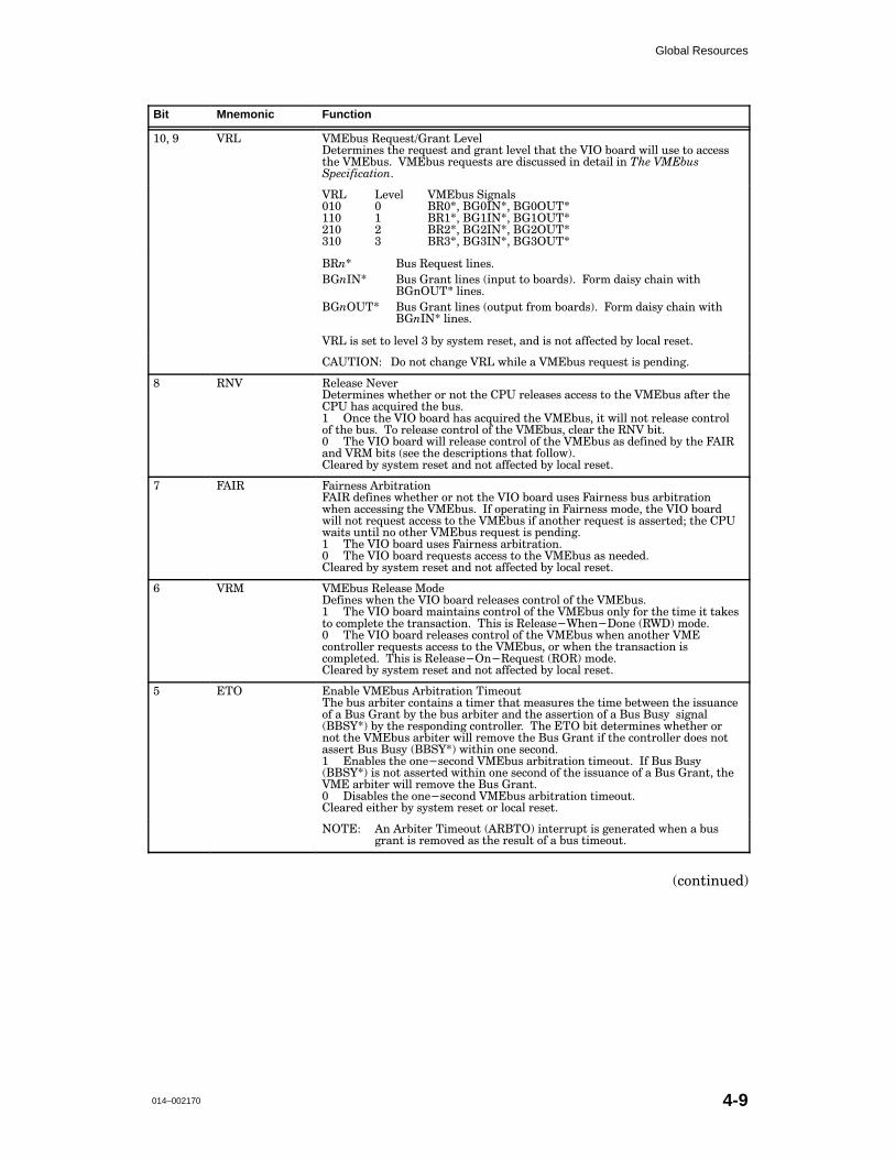
Global Resources
014–002170 4-9
Bit Mnemonic Function
� � %!� %��);9 !,7;,9:��8(4: �,<,2
�,:,8304,9 :/, 8,7;,9: (4+ .8(4: 2,<,2 :/(: :/, %�� )5(8+ =022 ;9, :5 (**,99
:/, %��);9� %��);9 8,7;,9:9 (8, +09*;99,+ 04 +,:(02 04 �� �������� � �� ���
%!� �,<,2 %��);9 "0.4(29
�!�� ������ ���$#�
�!�� ������ ���$#�
� � �!��� ������� ����$#�
� � �!��� ������� ����$#�
�!�� �;9 !,7;,9: 204,9�
������ �;9 �8(4: 204,9 �046;: :5 )5(8+9�� �583 +(09> */(04 =0:/
��4�$#� 204,9�
����$#� �;9 �8(4: 204,9 �5;:6;: -853 )5(8+9�� �583 +(09> */(04 =0:/
������ 204,9�
%!� 09 9,: :5 2,<,2 � )> 9>9:,3 8,9,:� (4+ 09 45: (--,*:,+ )> 25*(2 8,9,:�
��$#���� �5 45: */(4., %!� =/02, ( %��);9 8,7;,9: 09 6,4+04.�
� !�% !,2,(9, �,<,8
�,:,8304,9 =/,:/,8 58 45: :/, � $ 8,2,(9,9 (**,99 :5 :/, %��);9 (-:,8 :/,
� $ /(9 (*7;08,+ :/, );9�
�4*, :/, %�� )5(8+ /(9 (*7;08,+ :/, %��);9� 0: =022 45: 8,2,(9, *54:852
5- :/, );9� #5 8,2,(9, *54:852 5- :/, %��);9� *2,(8 :/, !�% )0:�
#/, %�� )5(8+ =022 8,2,(9, *54:852 5- :/, %��);9 (9 +,-04,+ )> :/, ���!
(4+ %!� )0:9 �9,, :/, +,9*806:0549 :/(: -5225=��
�2,(8,+ )> 9>9:,3 8,9,: (4+ 45: (--,*:,+ )> 25*(2 8,9,:�
� ���! �(084,99 �8)0:8(:054
���! +,-04,9 =/,:/,8 58 45: :/, %�� )5(8+ ;9,9 �(084,99 );9 (8)0:8(:054
=/,4 (**,9904. :/, %��);9� �- 56,8(:04. 04 �(084,99 35+,� :/, %�� )5(8+
=022 45: 8,7;,9: (**,99 :5 :/, %��);9 0- (45:/,8 8,7;,9: 09 (99,8:,+� :/, � $
=(0:9 ;4:02 45 5:/,8 %��);9 8,7;,9: 09 6,4+04.�
#/, %�� )5(8+ ;9,9 �(084,99 (8)0:8(:054�
#/, %�� )5(8+ 8,7;,9:9 (**,99 :5 :/, %��);9 (9 4,,+,+�
�2,(8,+ )> 9>9:,3 8,9,: (4+ 45: (--,*:,+ )> 25*(2 8,9,:�
� %!� %��);9 !,2,(9, �5+,
�,-04,9 =/,4 :/, %�� )5(8+ 8,2,(9,9 *54:852 5- :/, %��);9�
#/, %�� )5(8+ 3(04:(049 *54:852 5- :/, %��);9 542> -58 :/, :03, 0: :(1,9
:5 *5362,:, :/, :8(49(*:054� #/09 09 !,2,(9,�&/,4��54, �!&�� 35+,�
#/, %�� )5(8+ 8,2,(9,9 *54:852 5- :/, %��);9 =/,4 (45:/,8 %��
*54:8522,8 8,7;,9:9 (**,99 :5 :/, %��);9� 58 =/,4 :/, :8(49(*:054 09
*5362,:,+� #/09 09 !,2,(9,��4�!,7;,9: �!�!� 35+,�
�2,(8,+ )> 9>9:,3 8,9,: (4+ 45: (--,*:,+ )> 25*(2 8,9,:�
�#� �4()2, %��);9 �8)0:8(:054 #03,5;:
#/, );9 (8)0:,8 *54:(049 ( :03,8 :/(: 3,(9;8,9 :/, :03, ),:=,,4 :/, 099;(4*,
5- ( �;9 �8(4: )> :/, );9 (8)0:,8 (4+ :/, (99,8:054 5- ( �;9 �;9> 90.4(2
���"'�� )> :/, 8,9654+04. *54:8522,8� #/, �#� )0: +,:,8304,9 =/,:/,8 58
45: :/, %��);9 (8)0:,8 =022 8,35<, :/, �;9 �8(4: 0- :/, *54:8522,8 +5,9 45:
(99,8: �;9 �;9> ���"'�� =0:/04 54, 9,*54+�
�4()2,9 :/, 54,�9,*54+ %��);9 (8)0:8(:054 :03,5;:� �- �;9 �;9>
���"'�� 09 45: (99,8:,+ =0:/04 54, 9,*54+ 5- :/, 099;(4*, 5- ( �;9 �8(4:� :/,
%�� (8)0:,8 =022 8,35<, :/, �;9 �8(4:�
�09()2,9 :/, 54,�9,*54+ %��);9 (8)0:8(:054 :03,5;:�
�2,(8,+ ,0:/,8 )> 9>9:,3 8,9,: 58 25*(2 8,9,:�
��#�� �4 �8)0:,8 #03,5;: ��!�#�� 04:,88;6: 09 .,4,8(:,+ =/,4 ( );9
.8(4: 09 8,35<,+ (9 :/, 8,9;2: 5- ( );9 :03,5;:�
�*54:04;,+�

Global Resources
014–0021704-10
Bit Mnemonic Function
�� ������ � ���"42 �!3! �1!-2&%1 �),%.43 �%+%#3
��� $%3%1,)-%2 3(% +%-'3( .& 3),% 3(!3 3(% �!3! �31."%2 ����� !-$ �����
,423 "% !22%13%$ .- 3(% ���"42 "%&.1% 3(% ��� ".!1$ !22%132 ! �42 �11.1
�������� �& 3(% ��� ".!1$ �.#!3).- ����� ")3 )- 3(% ������� 1%')23%1 )2 2%3
3. �� 3(% 3),%1 )2 $)2!"+%$�
��� �%-'3( .& �!3! �31."%2
��� 42
��� �� 42
�� � 42
�� �)2!"+%$ �)-&)-)36�
��� )2 2%3 "6 2623%, 1%2%3 !-$ -.3 !&&%#3%$ "6 +.#!+ 1%2%3�
��� �-!"+% �!3#($.' �),%1
�(% 5!3#($.' 3),%1 #(%#*2 &.1 1%2/.-2%2 3. ��� )-3%114/3 1%04%232� �& 3(%
��� $.%2 -.3 1%2/.-$ 3. ! ��� )-3%114/3 1%04%23 5)3()- .-% 2%#.-$� 3(%
5!3#($.' 3),%1 )2 2%3� �()2 1%24+32 )- !- !#3).- !2 $%3%1,)-%$ "6 3(% ������
� ")32 .& 3()2 1%')23%1� ��-&.1,!3).- .- 3(% ��� ")32 &.++.52��
� �-!"+%2 1%!#3).-2 3. 5!3#($.' 3),%.432� �(%- 3(% 5!3#($.' 3),%1 )2
%-!"+%$ !-$ 2%3� !- !#3).- $%&)-%$ "6 3(% ��� ")32 )2 /%1&.1,%$�
� �)2!"+%2 1%!#3).-2 3. 5!3#($.' 3),%.432� �(% 5!3#($.' 3),%1 #!- "% 42%$
&.1 .3(%1 3),)-' &4-#3).-2�
��� )2 #+%!1%$ "6 %)3(%1 2623%, 1%2%3 .1 +.#!+ 1%2%3�
�� � ������ � �!3#($.' �#3).-
��� $%3%1,)-%2 5(!3 (!//%-2 5(%- 3(% 5!3#($.' 3),%1 )2 2%3 3. ��
Value inWDA Action �
�� �(% 2623%, /%1&.1,2 ! 2623%, 1%2%3�
��� �(% 2623%, /%1&.1,2 ! +.#!+ 1%2%3�
�� �(% 2623%, /%1&.1,2 ! +.#!+ 1%2%3 !-$ (.+$�
�� �(% 5!3#($.' 3),%1 )2 $)2!"+%$�
��� )2 2%3 "6 2623%, 1%2%3 !-$ )2 -.3 !&&%#3%$ "6 +.#!+ 1%2%3�
�#.-#+4$%$�
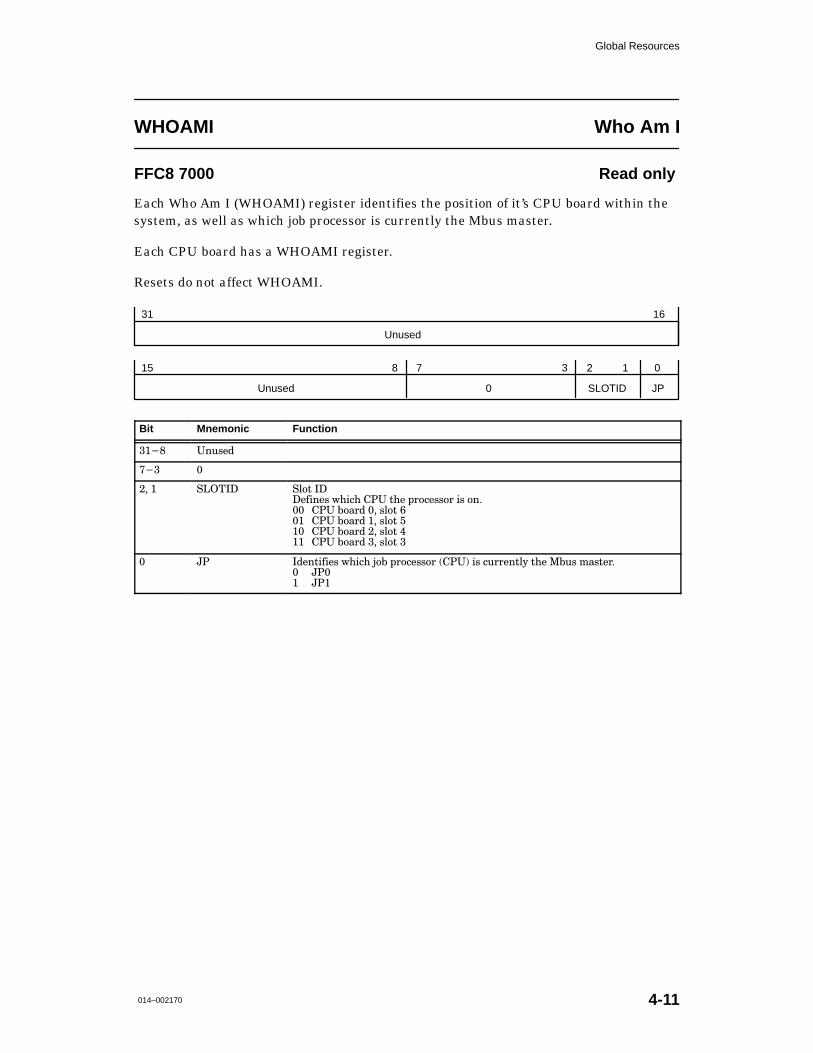
Global Resources
014–002170 4-11
WHOAMI Who Am I
FFC8 7000 Read only
Each Who Am I (WHOAMI) register identifies the position of it’s CPU board within thesystem, as well as which job processor is currently the Mbus master.
Each CPU board has a WHOAMI register.
Resets do not affect WHOAMI.
31 16
15 01238
Unused SLOTID JP0
Unused
7
Bit Mnemonic Function
��� �&,*��
�� �
� � ������ �$'+ ��
�� "&�* -!"�! ��� +!� ()'��**') "* '&�
�� ��� �'�)� �� *$'+
�� ��� �'�)� �� *$'+ �
�� ��� �'�)� � *$'+ �
�� ��� �'�)� � *$'+
� �� ���&+" "�* -!"�! #'� ()'��**') ����� "* �,))�&+$. +!� ��,* %�*+�)�
� ���
� ���

Global Resources
014–0021704-12
Global Control and Status (GCS) RegistersThis section describes the following Global Control and Status (GCS) registers:
GLOBALn Global registers 1 and 2BRDID Board ID registerGPCSn General-Purpose Control and Status registers 0–4
The GCS registers are accessed by VME controllers as well as by CPUs. The CPUs andVME controllers pass information via the GCS registers as follows:
• �# �� � * "$+, * �(',�$'+ ,# ��� �(�*� $� ',$!$��,$(' '-&� *�
• �# ������ * "$+, * )�++ + ,# %(��,$(' &('$,(*+�
• �# ����� * "$+, * #�'�% + +.+, & !�$% ����� $', **-),+ ,( ,# ����-+� #�'�% +
%(��% * + ,+� )�++ + ��� �'� ��� $', **-),+ ,( ,# ���+� �'� )�++ + ,# ��� �(�*�
%(��,$(' ,( ��� �(',*(%% *+�
• �# ����� * "$+, *+ )�++ -+ *�� !$' � ��,��
To access the GCS registers, a VME controller writes a 16–bit address of the GCSregister and defines the address as an A16 address via the address modifiers AM[5–0].The three most–significant nibbles of the address must be the same as the value definedby the BASAD register, which is loaded by the Group Address (GRPAD) and BoardAddress (BDAD) switches on the VIO board. When the VME controller defines andwrites an A16 address, the VME interface logic compares the address with the valuestored in the Base Address (BASAD) register. If the two addresses are the same, theaddress is placed on the Mbus. Bits A[3–0] of the address select one of the eight GCSregisters.
Unlike the other system registers, the GCS registers are not on word (4–byte)boundaries. If a VME controller attempts to write or read a word, a bus error isreturned. If a CPU accesses a word, the GCS logic returns two copies of the register’scontents.
CAUTION: When addressing a GCS register from the CPU, do not use the ExchangeMemory with Register (XMEM) instruction except via A16 (short I/O) space.This ensures that no other VME masters access the GCS registers betweenthe XMEM load and store operations.
The following pages define the Global Control and Status registers.

Global Resources
014–002170 4-13
BRDID Board ID
FFF8 6005 Read/Write (as noted)
Board ID (BRDID) contains the VIO board identification number. The VMEbus usesBRDID to identify the VIO board.
System resets clear BRDID, local resets do not affect BRDID.
BID
7 0
Bit Mnemonic Function
��� �� � �"� ����$�����$� �
� ��%# ���� ��'� �%# ������"�$�
%"��� ! &�"%!� $�� �� &"�$�# $�� ��� � �"� ����$�����$� � ��$ ��� ���
� ��%# ��� $��� "��� �� $ ��$ $�� ��� � �"� ��

Global Resources
014–0021704-14
GLOBAL0 Global Register 0
FFF8 6001 Read/Write (as noted)
Global Register 0 (GLOBAL0) defines the state of the location monitors and the VMEbusinterface chip identification number.
LM
7 034
CID
Bit Mnemonic Function
��� ������ ����., �)��-%)( �)(%-)+,
�!� ��+%-! �
�!"%(!, /$!-$!+ )+ ()- -$! &)��-%)( ')(%-)+ !-!�-! �( ���!,,�
&)��-%)( ')(%-)+ ���!,, /�, ()- !-!�-! �
� &)��-%)( ')(%-)+ ���!,, /�, !-!�-! �
�!- -) �0 ,0,-!' +!,!- �( ()- �""!�-! �0 &)��& +!,!-�
�� ��� ����.,���., �$%* � !(-%"%��-%)( �.'�!+
�!� )(&0�
�$! ��� �%-, �+! ,!- -) � %( %��-%(# -$�- -$! �&)��& �)(-+)& �( �-�-.,
����� +!#%,-!+, .,! -$! �)-)+)&� �!"!+!(�! �-�( �+ �
�)- �""!�-! �0 !%-$!+ ,0,-!' +!,!- )+ &)��& +!,!-�

Global Resources
014–002170 4-15
GLOBAL1 Global Register 1
FFF8 6003 Read/Write (as noted)
The GLOBAL1 register sets the Mbus reset, control, and status conditions and informsthe CPU of the status of these conditions.
R&H
7 6 5 01234
SBL ISF BDF 0 0 SHP SLP
Bit Mnemonic Function
� "�� �6+)3 "-9-:�)5,��63,
"-),'81:- *6:0 &��*;9 )5, �*;9
%9-, :6 8-9-: :0- �!% )5, ���%9
� "-9-:9 :0- �!% )5, ���%9
� �6-9 56: 8-9-: :0- �!% )5, ���%9
�3-)8-, *? 9?9:-4 8-9-: )5, 56: )..-+:-, *? 36+)3 8-9-:
� #�� &� *6)8, �6+):165
"-), 653? *6:0 &��*;9 )5, �*;9
#�� 19 0)8,=18-, :6 9=1:+0 �� �#� �� 6. ��! 9=1:+0 # ������ '0-5 8-),�
#�� 4;9: *- ) �� 15,1+):15/ :0): :0- &� *6)8, 19 15 &�� 936: � )5, 9;773?15/
#(#��� )5, ���" :6 :0- &��*;9 �. #�� 19 �� +0-+2 :0- #� � 9=1:+0
� �5,1+):-9 :0): :0- #� � 9=1:+0 19 65� :0- &� *6)8, 19 15 &�� 936: � )5,
9;773?15/ #(#��� )5, ���" :6 :0- &��*;9
� �5,1+):-9 :0): :0- #� � 9=1:+0 19 6..� :0- &� *6)8, 19 56: 15 936: � )5, 19
56: 9;773?15/ #(#��� )5, ���" :6 :0- &��*;9
�6: )..-+:-, *? 8-9-:9
� �#� �501*1: :0- #(#����� 6;:7;: :6 :0- &��*;9
"-),'81:- *6:0 &��*;9 )5, �*;9
�-:-8415-9 =0-:0-8 68 56: :0- &� *6)8, =133 7)99 ) 9?9:-4 8-9-: 65 :6 :0-
&��*;9 �#(#"�#�$� 315-�
� $0- &� *6)8, =133 56: )99-8: #(#����� 65 :0- &��*;9
� �99-8: #(#����� 1. �#�� 6. :0- %�# 8-/19:-8 19 )99-8:-, 68 1. :0-
=):+0,6/ :14-8 0)9 ->718-,
�3-)8-, *? 9?9:-4 8-9-: )5, 56: )..-+:-, *? 36+)3 8-9-:
� ��� �6)8, �)13 #:):;9
"-), 653? *6:0 &��*;9 )5, �*;9
�5,1+):-9 =0-:0-8 :0- &� *6)8, 19 151:1):15/ ) 9?9:-4 .)13;8- �1-� 1: 15,1+):-9
:0- 9:):- 6. :0- �#�� *1: 6. :0- %�# 8-/19:-8 )5, :0- 6;:7;: 9:):- 6. :0-
=):+0,6/ :14-8�
� �99-8: #?9:-4 �)13;8- ��#��� 6. :0- %�# 8-/19:-8 19 )99-8:-, ���� 68 :0-
=):+0,6/ :14-8 19 9-: �:0- :14-8 0)9 ->718-,�
� �#�� 19 56: )99-8:-,� )5, :0- =):+0,6/ :14-8 6;:7;: 19 +3-)8-,
�6: )..-+:-, *? 8-9-:9� ��� )3=)?9 8-.3-+:9 :0- 9:):- 6. �#�� )5, :0-
=):+0,6/ :14-8 6;:7;:
��� "-9-8<-, �3=)?9 �

Global Resources
014–0021704-16
GPCSn General–Purpose Control and Status
FFF8 6007 GPCS0 Read/Write
FFF8 6009 GPCS1
FFF8 600B GPCS2
FFF8 600D GPCS3
FFF8 600F GPCS4
The General–Purpose Control and Status (GPCSn) registers allow programmer–definedcontrol and status information to be passed from one VME controller to another over theVMEbus. If a VME controller writes control and status into a GPCSn register, othercontrollers can read the GPCSn register and use the information. The programmerdefines the functions of the bits in these registers.
NOTE: For good programming structure, the GPCSn registers should be used only topass control and status information between VME controllers (including theVIO board).
GPCS
7 0
Bit Mnemonic Function
��� ��� ����!�� �$! �"� ��#!�� ��� �#�#$"
��� !��!����! ������" #�� �$��#��� �� #�� �����&�� ��#"�
� "%"#�� !�"�# "�#" ���� #� ��� � "%"#�� !�"�# ����!" ���� #�!�$��
����� ���� !�"�#" �� ��# �����# #�� ���� !���"#�!"�
�� �� �� #�!

014–002170 5-1
Chapter 5Memory
This chapter describes the types of memory available on the CPU board, VIO board andmemory boards. All RAM is located on memory boards that contain Error Checking andCorrection (ECC) logic. The VIO board has Programmable Read–Only Memory (PROM)which contains boot code. The system configuration parameters are stored innon–volatile RAM (NOVRAM) as described in Chapter 7, “Programming theCounter/Timer and the Real-Time Clock”. Access to memory is regulated by memorymaps. CPUs can access all of memory, but VME controllers can access only resourcesallowed by the VME address map.
Interleaved MemoryMemory is interleaved among the two or four available memory boards. This sectiondescribes how memory is interleaved.
Logical addresses on the Mbus bound for system memory are decoded and permutedbefore being written to the X0bus or the X1bus. Bit 4 of the Mbus address points toeither the X0bus (bit 4=0) or the X1bus (bit 4=1). The LMAD decodes the upper tenaddress bits, and selects either memory board 0 or memory board 1 on the selected bus(X0 or X1). Bit 24 of the Mbus address is written into bit 4, and bits 25–29 are shiftedone bit position into bits 24–28. This address is written to the selected bus (X0 or X1)and into the selected memory board on that bus (mem 0 or mem 1). The example below,and Figure 5–1 illustrate interleaving.
EXAMPLE: Assuming you have four 64-Mbyte memory boards, the addresses decode as follows:
0000 0001 0000 0000 0000 0000 0000 0000 Mbus0000 0000 0000 0000 0000 0000 0001 0000 X0busDecodes to X0bus, memory board 0
0000 1000 0000 0000 0000 0000 0000 0000 Mbus0000 0100 0000 0000 0000 0000 0000 0000 X0busDecodes to X0bus, memory board 1
0000 0000 0000 0000 0000 0000 0001 0000 Mbus0000 0000 0000 0000 0000 0000 0000 0000 X1busDecodes to X1bus, memory board 0
0000 1001 0000 0000 0000 0000 0001 0000 Mbus0000 0100 0000 0000 0000 0000 0001 0000 X1busDecodes to X1bus, memory board 1
Bit 26 of the Mbus selects mem 0 or mem 1 when have 64MB boardsBit 27 of the Mbus selects mem 0 or mem 1 when have 128MB boardsBits 26 and 27 combined select mem 0 or mem 1 when have 192MB boards

Memory
014–0021705-2
1–03–2423–528–2431–29
1–03–2423–529–2531–30 24
64 MB wedge
64 MB wedge
64 MB wedge
64/128/192 MB board
X0bus Address X0bus Data
Mbus
X0busor
X1bus
Mbus:Bit 4 selects Xbus (cache block) (0=X0bus, 1=X1bus)Bits 31–20 are always 0 for system memory.
X0/X1bus:Bits 23–0 select the address within a bankBits 28–24 select the board and wedgeBits 31–29 are always 0 for system memory.
Bank 016 MB
64/128/192 MB board
64/128/192 MB boardX1bus Address X1bus Data
64/128/192 MB board
Bank 116 MB
Bank 316 MB
Bank 216 MB
� �������� ��������� ������ � ������ ����� ��

Memory
014–002170 5-3
Reading from MemoryWhen a device reads data from memory, memory sources the data at a rate of one wordper bus cycle until it receives an EOR (End of Request) from the reading device or untilthe read crosses to a new block of data. If the block crossing occurs first, the memorymodule asserts End of Data (EOD). Block crossings are described in the “Data Blocksand Block Crossing” section earlier in this chapter.
When data is read, memory examines the data for single–bit and multiple–bit errors.When a multiple–bit error occurs, a bus error is asserted and an exception routine mustbe run. When a single–bit error occurs, the error correction logic asserts two wait stateswithin which the logic corrects the data and writes the corrected data to the data bus.The error logic also notifies the interrupt logic that a single–bit error has occurred. Aninterrupt service routine can then update the error log. Single–bit errors are correctableand do not affect address flow. Memory boards do not correct data when written to; theyonly correct data when read from. The “Error Checking and Correction (ECC)” sectionlater in this chapter describes the error checking process in greater detail.
When a CPU or a VME controller reads a block (4 words) of data from memory, thefollowing occurs:
1. �� �� �� ��� ���������� ����� ��� �������� ������� �� �����"�
2. �� �����" ������ �������� ��� ��������
3. �� ��� �����" ������ ������ ������� �� ��� ������� ����� ��� ����� �"���� ��������" ������ ������� ��� ������� �� ���� �������� ��������� ��� ��� ��� �����
�� ��������
4. �� �� �� ��� ���������� ����� � ��� �� ���� ���� �����"�
5. �� �����" ������ ������������" ���������� ��� ������� �� ��� ��!� ��� �� ��������� ����� ���� ��� �� ���� �� ��� � ��� ��� ������� ��������� ����� ��� �������
������� ��� ��� �� ��� ���� �����
Writing to MemoryMemory receives data (in bytes, half–words or words) until it receives an End of Request(EOR) or until a block crossing occurs.
The master writes a word on the data bus and the addressed memory receives the data.The memory module generates ECC bits and writes them to memory with the data. Ifthe data transfer is a byte or half–word, the CPU performs a read–modify–writeoperation to generate the ECC bits. Read–modify–write operations extend the writecycle.
When a CPU or VME controller writes a block of data to memory, the following occurs:
1. �� �� �� ��� ���������� ����� ��� �������� ������� �� �����"�
2. �� �����" ������ �������� ��� ��������

Memory
014–0021705-4
3. �� �� � ���� ����� ����� � ����� �� �� ��� �� ������ �� ����� ���� � �� ��� ���
��� ��� �� �� �� ����� � ������� � �� � �� ��� ��� �� � ��� ��
4. �� ��� ���� � ���� �� �� �� � ����� �� �� � ���� ����� ���� � �� ��
���� � �����
5. �� � ���� ����� ���������� ���� � ��� �� ��� �� �� �� � �� ����� �� �
���� � ��� ���� �� �� ���� �� � ����� ���� ���� �� ������� � ����� �� ��� ��
� �� � �� �� �� �� �� �����
Data Blocks and Block CrossingData is transmitted as single words, asserting a new address after each word, or asblocks with an address asserted at the beginning of the block. This section describes twodata blocks: CMMU and VME data blocks.
CMMU BlockA block (cache line) of data, as defined by the CMMUs, is four 32-bit words of data thatwhen read from or written to memory, are aligned on an even address whoseleast–significant nibble begins at address 016. Figure 5–2 illustrates a block of data asdefined by the CMMUs.
1 block = 4 words = 16 bytes
1 word
1 word
1 word
1 word
1 block
1 word
1 word
1 word
1 word
00
04
08
0C
10
14
18
1C
Block address range is 0 to F.
����� ���� � ���� ������
When a CPU reads a block of data from memory or writes a block of data to memoryusing an aligned read or write as just described, the read or write will complete within10 bus cycles. If the read or write crosses from one block to another (called a blockcrossing), the transfer will require an additional bus cycle.
VME BlockA block of data, as defined by VME controllers, is the largest entity of data that thecontroller’s buffer can receive within a burst read or a burst write. A burst is a transferof a block of data without CPU intervention; memory automatically increments theaddress. Each controller establishes its block size and must communicate this size to themaster controller.

Memory
014–002170 5-5
Cache CoherencyThe CMMUs contain cache memory (called cache) as temporary storage to speed upinstruction execution. If the cache is turned off, the CPU interacts directly with systemmemory (called memory). When the cache is turned on, the CPU reads from and writesto memory through the cache. When the cache is turned on, the CMMUs updatememory using either Writethrough or Copyback mode. When the cache is operating inWritethrough mode, all modifications to the cache are immediately written to memory.When the cache is operating in Copyback mode, only the first modification of each cachelocation is written to memory. When memory is read, accurate data is expected.
Cache coherency is a property of the CMMUs and memory to pass correct data whenmemory is read. If the cache is turned off, or if the cache is on and in Writethroughmode, memory is always current because the CPUs write changed data directly tomemory. If the cache is on and updated in Copyback mode, locations in memory may notbe current because the changed data is written only to the respective cache, not to thememory.
If the cache is on and in Copyback mode, the CMMUs snoop the Mbus for accesses tolocations that have been modified by a CPU. If a modified location is read, theappropriate CMMU updates the location before the read is completed. Figure 5–3illustrates cache coherency. For a detailed description of cache coherency and Mbussnooping, see either the MC88200 Cache/Memory Management Unit User’s Manual, orthe MC88204 Cache/Memory Management Unit User’s Manual.
A device writes an address to the Mbus.
The CMMU snoops the Mbus address and checksthe cache location to determine if the data has beenmodified. Yes
No
The device reads the data from memory.
The CMMU issues a RETRY signal via theSS[3–0] lines. This prevents the devicefrom reading the memory location until afterthe CMMU has updated the memorylocation.
The CMMU updates the memory location,writing from cache to memory.
The CMMU clears the cache modify bit to 0.
The CMMU relinquishes the Mbus.
The device accesses the Mbus andreads the data from memory.
Is the data incache?
Has the databeen modified?
Yes
No
�������� ���� ���� ��

Memory
014–0021705-6
The System Status LinesThe system status lines (SS[3–0]) on the Mbus pass bus information to or from the CPU.This information includes:
Error �((&( !%�!��*�) * �* � �+) �((&( &��+((��� � !) $��%) * �* �% !%,�#!�
���(�)) -�) ����))��� � $+#*!'#���!* � �((&( &��+((��� &( � ����+)
*!$��&+* &��+((��� � �% �% �((&( &��+()� * � �+((�%* $�$&(/
&'�(�*!&% !) ��&(*���
Retry � � ���) ��%�(�*� * � ��*(/ )!�%�# *& !%�!��*� * �* � $�$&(/
#&��*!&% * �* !) ��!%� (��� �) )*�#� ��*�� ��*(/ !) +)�� - �% ��� �
�& �(�%�/ !) �%��#�� �%� * � ���) �&%*�!% ��*� * �* �) ���%
$&�!�!�� �+* %&* -(!**�% *& $�$&(/� � �% ��*(/ !) �))�(*��� * �
(���!%� ��,!�� -�!*) �&( * � ��� *& +'��*� * � $�$&(/ #&��*!&%
���&(� (���!%� * � ��*��
Wait ��$&(/ ��,!��) �))�(* � ��!* - �% * �/ ��% %&* (��� &( -(!*� ��*�
-!* !% &%� �#&�" �/�#� ��!* �.*�%�) * � ��*� ' �)�� � $�$&(/ ��%%&*
(�)'&%� *& �% ���(�)) -!* !% &%� �#&�" �/�#�� * � $�$&(/ $&�+#� �(!,�)
* � ��� #!%� �&- *& !%)�(* -�!* �/�#�) +%*!# !* !) (���/ *& (���!,� &( )�%�
��*��
End of Data ��$&(/ �))�(*) �% �%� &� ��*� - �% � ��*� *(�%)��( �) �&$'#�*��
)+���))�+##/�
OK �� !%�!��*�) * �* * � '(�,!&+) �+) �/�#� �&$'#�*�� )+���))�+##/ �%� * �
�&$'+*�( )/)*�$ !) (���/ *& '(&��)) � %�- �+) �/�#��
As you can see from Table 5–1, each status line defines a system condition.
Table 5–1 System Status Lines
SS3 SS2 SS1 SS0 Function
� � � � �((&(
� � � � ��*(/
� � � � ��!*
� � � � �%� &� ��*� ���*� ' �)��
&(
�� ����(�)) ' �)��
� � � � �� �' �)� �&$'#�*���
SS3 indicates an Error when Low;SS2 indicates a Retry when Low;SS1 indicates a Wait when Low; andSS0 indicates an End of Data when Low.
An address phase is the period during which an address is written to and stabilized onthe bus, and successfully interpreted by the addressed device. A data phase is the timeduring which data is successfully transferred over the bus.
When all of the system status lines are High, the computer system is OK and ready tostart a new bus cycle.

Memory
014–002170 5-7
Error Checking and Correction (ECC)The memory boards each examine data read from RAM for errors, and correct single–biterors, but not multiple–bit errors. The process of finding and correcting memory errorsis called Error Checking and Correction (ECC). When a single–bit error occurs, theinterrupt logic interrupts a CPU, which logs the error and runs an interrupt serviceroutine. Multiple–bit errors cannot be corrected.
Each memory board has on–board memory refresh; memory is refreshed every 15.6 ms.If an Mbus transaction is taking place, a memory refresh will occur after the Mbustransaction is completed. While memory is being refreshed, the WAIT status is pending.
All ECC errors are reported to the processors through the IST register’s MEM bit.Perform the following steps to clear an ECC error:
1. Shut down all processes that access system memory.
2. Disable the MEM interrupt by clearing the IEN register’s MEM bit to 0.
3. Find the error as follows:
A. Read an ERAx register.
B. Read the corresponding CONx register.
C. Check bit 26 (SBE) for a single–bit error. If set, continue with step 4. If cleared,continue with step A for the next register.
4. Build the error offset for the logical memory board as follows:
A. Shift bits 27–24 left 1 bit.
B. Copy the value in bit 4 to bit 24.
C. If the error was found on CON1 or CON3, clear bit 4 to 0.If the error was found on CON2 or CON4, set bit 4 to 1.
5. Add the starting address for the logical memory board.
6. Read the location.
7. Execute XMEM to write the value back to memory.
8. Set the GIEN MEM bit to 1 to enable the MEM interrupt.
RegistersThis section describes the Control (CON) register and the Error Address (ERA) register.The Control register regulates memory refresh, error detection and correction, memorysize, and system diagnostics. The Error Address register contains the address of thefirst error that occurred since the last time that ERA was read. The following pagesdescribe the CON and ERA registers.

Memory
014–0021705-8
CONx (Resides on memory boards) Control
FFF8 9100 CON1 – X0bus, Board 0 Read/Write
FFF8 9110 CON2 – X0bus, Board 1
FFF8 9300 CON3 – X1bus, Board 0
FFF8 9310 CON4 – X1bus, Board 1
The Control (CON) register maintains memory status and control.
31 16
15 0
SBE
212223
Reserved
2730
WAITS
29
DMRCPUCLK Reserved
26
MBE
25 24
LED DLE MOD ERE COE
17181920
MEM
1213
ECB
67
Reserved
Bit Mnemonic Function
� � $��� � $ �14)0 "5++*
� $��� /7 7+8 84 � *96/3- 54;+695� *4 ��� 7+8 � $��� 84 �
� ��>
� ��>
�� %��#" �92(+6 4, %'/8 "8'8+7
%��#" /7 7+8 84 � *96/3- 54;+695� *4 348 7+8 %��#" 84 �
� ;'/8 78'8+7 �$7+ 8./7 7+88/3- ;/8. � ��> � $����
� � ;'/8 78'8+7 �$7+ 8./7 7+88/3- ;/8. ��> � $����
��� !+7+6:+*
� "�� "/3-1+ �/8 �6646
"/3-1+ (/8 +6646 4))966+*�
� �4 +6646�
!+7+6:+*
� ��� �918/51+ �/8 �6646
�918/51+ (/8 +6646 4))966+*�
� �4 +6646�
�� ��� �/'-3478/) ��� �438641
��� )4386417 8.+ 45+6'8/43 4, 8.+ */'-3478/) ���7 14)'8+* 43 8.+ 7=78+2
(4'6*� #.+ !�� ��� 5917+7 ,46 �� 27 ;.+3 ' )466+)8'(1+ +6646 /7 *+8+)8+*�
'3* 6+2'/37 1/8 ;.+3 '3 93)466+)8'(1+ +6646 /7 *+8+)8+*� #.+ &����% ���
1/-.87 ;.+3 '3 +<51/)/8 6+'*�;6/8+ '))+77 /7 *+)4*+*� 931+77 /8 /7 4:+66/**+3 (=
&� 46 &��� #.+ �!��� ��� 1/-.87 ;/8. +:+6= 6+,6+7. )=)1+�
Bits Mode�� !93 � 8.+ ���7 45+6'8+ '7 *+7)6/(+* '(4:+�
� !�� � 6+7+87 8.+ 6+* ��� �)1+'67 6+* 84 � �4,,��
� &�� � 8.+ =+114; ��� 6+2'/37 4,, �931/8�
&� � 8.+ =+114; ��� 6+2'/37 43 �1/8�
��� �/'-3478/) �'8). �3'(1+
�3'(1+7 8.+ 1'8)./3- 4, ��� (/87 /384 8.+ ��� ).+)0 (/87 ����� (/87 ���� 4,
8.+ ���< 6+-/78+6�
�3'(1+ 8.+ 1'8)./3- 4, ��� (/87 /384 8.+ ��� (/87�
� �/7'(1+ 8.+ 1'8)./3- 4, ��� (/87 /384 8.+ ��� (/87�
�)438/39+*�

Memory
014–002170 5-9
Bit Mnemonic Function
�� �� ��� �%�#)*-.%� (* ! -!'!�.
Bits Mode�� �*,(�' *+!,�.%*)�
�� �%�#)*-.%� #!)!,�.!�
�� �%�#)*-.%� !.!�.
�� ��� �,,*, �)��'!
�)��'!- *, %-��'!- .$! ,!+*,.%)# *" -%)#'!5�%. �) (/'.%+'!5�%. !,,*,-�
� �)��'! ��� !,,*, ,!+*,.%)#�
� �%-��'! ��� !,,*, ,!+*,.%)#�
������ ����� ���� ���� ��� �� ��� �� ��� � ��������� ������ ��������
�� ��� �*,,!�. �)��'!
� �)��'! ��� !,,*, �*,,!�.%*)�
� �%-��'! ��� !,,*, �*,,!�.%*)�
������ ����� ���� ���� ��� �� ��� �� ��� � ��������� ������ ��������
� ��� �%-��'! �!(*,3 �!",!-$
� �%-��'! ���� ,!",!-$�
� �)��'! ���� ,!",!-$�
������ ����� ��� ���� ��� �� ��� �� ��� � ��������� ������ ��������
���� ��� �!(*,3 �%4!
�$!) ,!� � %) %��.!- $*1 (/�$ (!(*,3 %- *) .$�. (!(*,3 �*�, � �* 0!,%"3
.$! .*.�' -3-.!( (!(*,3� ,!� .$! ��� �%.- *) �'' *" .$! �0�%'��'! ���2
,!#%-.!,-�
Bits Memory Size��� � ��3.!-
��� �� ��3.!-
��� �� ��3.!-
��� �!-!,0!
�� ��� ��� �$!�& �%.-
��*)�'/ ! �

Memory
014–0021705-10
ERAx (Resides on memory boards) Error Address
FFF8 9104 ERA1 – X0bus, Board 0 Read only
FFF8 9114 ERA2 – X0bus, Board 1
FFF8 9304 ERA3 – X1bus, Board 0
FFF8 9314 ERA4 – X1bus, Board 1
The Error Address (ERA) register contains the address of the first error that occurredsince the last time that a CPU read the CONx register.
����� �� . -!"" $%* )*%(� � $�- �((%( ���(�)) +$*!" * � �.!)*!$� ���(�)) �) ���$
(���� �� #%(� * �$ %$� �((%( %��+() ��*-��$ (���)� %$"/ * � �!()* �((%(
���(�)) !) )*%(��� )+�)�'+�$* �((%( ���(�))�) �(� $%* (��%(����
ERA
31 16
15 0
ERAUnused
24 23
Bit Mnemonic Function
���� �$+)��
���� �� �((%( ���(�))
�%$*�!$) �!*) ����� %� * � ���(�)) %� � )!$�"���!* %( #+"*!&"���!* �((%(� � !)
�((%( !) * � �!()* �((%( * �* %��+((�� )!$�� * � "�)* *!#� * �* � ��� (���
���.� �$*�(,�$!$� �((%( ���(�))�) �(� $%* "�*� �� !$*% �� �
�$� %� � �&*�(

014–002170 6-1
Chapter 6Programming the Serialand Parallel Interfaces
���� ������� ��������� ��� ������ ��� �������� ����������� ����� ��������!� ������ ��� ��" ��
������� ��� �����������
The Serial and Parallel Interfaces��� �#���� ����� ��� �"� � ����� ������ ��#������� � ������ ��� ���
�������������������� �������� ����� ��� ������ ���� �� � �������� ���� ��� ��� �#����
�������� "���� ��� ����� ��� ����� ����� ��� ��� ������ � ������ �������� �� ��������
��� ������ ����� ��� �������� ��� �����!� ����� "���� ��� �������� ���� �� ������� ��
������������ ���� ���#� �� ������ ��� ������� ��� ������ ��� �������� �����������
DUART (SCN2681)
Channel A Channel B
Vbus
8 bits Control Logic andAddress Decode Logic
ParallelInterface
Parallel Port
32 bits8 bits
Transceiver
RS–232–CDrivers andReceivers
System Console Modem or Terminal
RS–232–CDrivers andReceivers
Serial Interface
����� ���� � � ��� �� ���� � ��� ��� �

Programming the Serial and Parallel Interfaces
014–0021706-2
Serial Interface�*' 4'3+#- +/5'3(#%' %0/4+454 0( # �+)/'5+%4 ����� �6#- �4:/%*30/064
�'%'+7'3��3#/4.+55'3 �� ����� �*' � ��� *#4 580 %*#//'-4� %*#//'- � (03 # 4:45'.
%0/40-' #/& %*#//'- � (03 # .0&'. 03 5'3.+/#-� �03 &'4%3+15+0/4 0( 5*' 4+)/#-4� 4''
�11'/&+9 �� �*' � ��� %-0%, +/165 +4 ������ �*;�
Parallel Interface�*' 1#3#--'- +/5'3(#%' 53#/4.+54 # 50 # 1#3#--'- 4-#7' &'7+%' 64+/) 5*' �'/530/+%4
13050%0-� �*' 1#3#--'- +/5'3(#%' *#4 # ��$:5' $6(('3� 5*'3'(03' :06 %#/ 53#/4.+5 #4
.#/: #4 %*#3#%5'34 #5 # 5+.'� !*'/ 5*' �%*#3#%5'3 13+/5'3 $6(('3 (+--4� 5*'
+/5'3(#%' %-'#34 5*' �3+/5'3 �6(('3 �.15: ����� $+5 +/ 5*' �/5'33615 �5#564 ����� 3')+45'3�
!*'/ 5*' 13+/5'3 $6(('3 '.15+'4� 5*' +/5'3(#%' 4'54 5*' ��� $+5� #/& 5*' �� %#/ 4'/&
.03' #� �*' 1#3#--'- 1035 1+/ #44+)/.'/54 #3' &'(+/'& +/ �11'/&+9 ��
Programming the Serial Interface�*' 4'3+#- ��� %0/4+454 0( 580 ��� %*#//'-4 8+5*+/ 0/' � ���� �*'4' %*#//'-4 .645 $'
%0/(+)63'& 7+# 5*' � ��� 3')+45'34 $'(03' 5*': 3'%'+7' 03 4'/& #� �0 130)3#. 5*'
� ���� 83+5' 50 +54 %0..#/& 3')+45'34� �0 )'5 � ��� 45#564 +/(03.#5+0/� 3'#& 5*'
� ����4 45#564 3')+45'34�
�*#/)+/) 5*' %0/5'/54 0( # 3')+45'3 8*+-' 5*' � ��� +4 53#/4.+55+/) 03 3'%'+7+/) #
.#: %#64' '33034� �03 '9#.1-'� %*#/)+/) 5*' /6.$'3 0( $+54 1'3 %*#3#%5'3 8*+-'
53#/4.+55+/) # .#: %#64' 5*' 53#/4.+44+0/ 0( #/ +/%033'%5 %*#3#%5'3� �0 /05 83+5' 50
5*' �0&' 3')+45'34� 5*' �-0%, �'-'%5 3')+45'34� 03 5*' �65165 �035 �0/(+)63#5+0/ 3')+45'3
8*+-' 5*' 3'%'+7'34 #/& 53#/4.+55'34 #3' '/#$-'&� �-40� &0 /05 83+5' 50 5*' �69+-+#3:
�0/530- 3')+45'3 8*+-' 5*' %06/5'3�5+.'3 +4 '/#$-'& �36//+/)��
�� ����� �0(58#3' .645 /05 +446' 4'26'/5+#- 3'#&4 #/&�03 83+5'4 50 5*' � ���
3')+45'34 $'%#64' 0( 5*' 4-08 4'561 5+.+/) (30. 3'#&�83+5' +/#%5+7' 50
3'#&�83+5' #%5+7' 41'%+(+'& $: �+)/'5+%4� "06 4*06-& 165 580 /0/01'3#5+7'
+/4536%5+0/4 $'58''/ 3')+45'3 3'#& #/& 83+5' +/4536%5+0/4�
�*' 3'45 0( 5*+4 4'%5+0/ &'4%3+$'4 5*' (0--08+/) 5#4,4�
• �30)3#..+/) 5*' � ��� 3')+45'34�
• �/+5+#-+;+/) 5*' 4'3+#- +/5'3(#%'�
• �'4'55+/) 5*' 4'3+#- +/5'3(#%'�

Programming the Serial and Parallel Interfaces
014–002170 6-3
Registers
�(% 2%1)!+ )-3%1&!#% 1%')23%12 !1% !##%22%$ !2 6.1$2 !-$ !1% !+)'-%$ .- 6.1$ ".4-$!1)%2�
�!#( #(!--%+ (!2 )32 .6- �.$%� �.,,!-$� �+.#* �%+%#3� !-$ �3!342 1%')23%12�
�++ 1%')23%12 !1% ,!//%$ 3. !$$1%22%2 ���� ��� 3(1.4'( ���� � ��� )- 3(% 2823%,�2
!$$1%22 2/!#%� �!"+%���� +)232 3(% 1%')23%12 !-$ 3(%)1 !$$1%22%2�
Table 6–1 Serial Interface Registers
���� � �.$% �%')23%12 � ������ ����� 1%!$61)3%
���� �� �3!342 �%')23%1 � ����� 1%!$
�+.#* �%+%#3 �%')23%1 � ������ 61)3%
���� �� �.,,!-$ �%')23%1 � ����� 61)3% �
���� �� �%#%)5% �.+$)-' �%')23%1 � ������ 1%!$
�1!-2,)3 �.+$)-' �%')23%1 � ������ 61)3%
���� �� �-/43 �.13 �(!-'% �%')23%1 ������ 1%!$
�47)+)!18 �.-31.+ �%')23%1 ����� 61)3%
���� ��� �-3%114/3 �3!342 �%')23%1 ����� 1%!$
�-3%114/3 �!2* �%')23%1 ����� 61)3%
���� ��� �.4-3%1�),%1 //%1 �%')23%1 ��� � �� �� 1%!$61)3%
���� ��� �.4-3%1�),%1 �.6%1 �%')23%1 ����� ����� 1%!$61)3%
���� �� �.$% �%')23%12 � ������ ����� 1%!$61)3%
���� ��� �3!342 �%')23%1 � ����� 1%!$
�+.#* �%+%#3 �%')23%1 � ������ 61)3%
���� ��� �.,,!-$ �%')23%1 � ����� 61)3% �
���� ��� �%#%)5% �.+$)-' �%')23%1 � ������ 1%!$
�1!-2,)3 �.+$)-' �%')23%1 � ������ 61)3%
���� � �%2%15%$
���� � � �-/43 �.13 1%!$
�43/43 �.13 �.-&)'41!3).- �%')23%1 ������ 61)3%
���� � � �3!13 �.4-3%1 �.,,!-$ 4-42%$
�%3 �43/43 �.13 �)32 �.,,!-$ 4-42%$
���� � � �3./ �.4-3%1 �.,,!-$ 4-42%$
�%2%3 �43/43 �.13 �)32 �.,,!-$ 4-42%$
Address Register Type of(A is the serial port; B is the mouse port) Register
� �. -.3 1%!$ ��� .1 ���� �%!$)-' 3(%2% 1%')23%12 ,!8 (!-' 3(% !28-#(1.-.42 +)-%�
��& 8.4 42% 3()2 +)-% &.1 3(% 2823%, #.-2.+%� 3(% 2823%, ,!8 (!-' !-$ 1%04)1% ! 1%2%3��

Programming the Serial and Parallel Interfaces
014–0021706-4
Initializing the Serial Interface�( ,)��#�% #'#-#�%#2�-#(' )+(��,, #, '���,,�+1�
Resetting the Serial Interface�"� ,�+#�% #'-�+ ��� #, +�,�- �#-"�+ �.+#'! )(0�+.) (+ /#� -"� ����� ��,�- ���� �#- ��
�#- ( -"� ('-+(% � ��� +�!#,-�+ �, ��,�+#��� #' "�)-�+ � 3��&(+1�� ��+-, ( -"�
����� ��' �� +�,�- /#� -"� (&&�'� +�!#,-�+, � �� �'� ��� �, ��,�+#��� #' -"�
(%%(0#'! +�!#,-�+ ��,�+#)-#(',�
Serial Interrupts�"� ����� &�1 !�'�+�-� ,�/�+�% -1)�, ( #'-�++.)-,� �.- #- "�, ('%1 ('� #'-�++.)- %#'�
0"#�" ,�-, -"� ����� �'-�++.)- ���� �#- #' -"� �'-�++.)- �-�-., ����� +�!#,-�+� �"�' -"�
�� ��$'(0%��!�, -"� #'-�++.)-� #- +���, -"� ������, �'-�++.)- �-�-., ��!#,-�+ �����
�'� "�'�%�, -"� #'-�++.)- �, '������ �'1 ( -"� (%%(0#'! �('�#-#(', ��' !�'�+�-� �'
#'-�++.)-�
• "�''�% � (+ � -+�',&#--�+ #, +���1�
• "�''�% � (+ � +���#/�+ #, +���1� (+ #-, ���� �. �+ #, .%%�
• "�''�% � (+ � ��-��-�� � �+��$ "�+��-�+�
• �"� #').- )(+- �"�'!�� ,-�-��
�"� )+(!+�&&�+ ��' &�,$ ,�+#�% #'-�++.)-, /#� -"� ������, �'-�++.)- ��,$ ��!#,-�+
������ �"�' �' #'-�++.)- #, &�,$��� -"� ����� 0#%% '(- ,�- -"� �#- #' -"� ���� �'�
�(',�*.�'-%1 0#%% '(- �,,�+- -"� ��� %#'� -( -"� ��� +�!#,-�+ (+ -"�- #'-�++.)-�
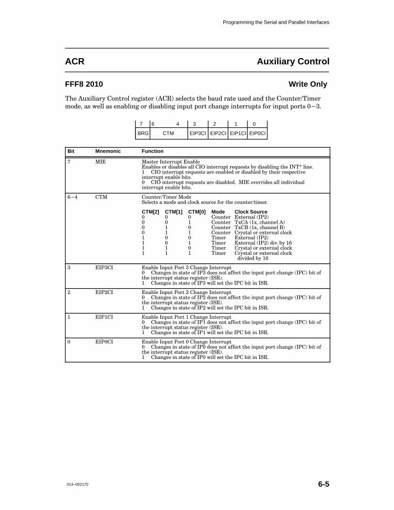
Programming the Serial and Parallel Interfaces
014–002170 6-5
ACR Auxiliary Control
FFF8 2010 Write Only
�# �/2$&$�,3 �)(.,)& , "$-. , ����� - & �.- .# ��/� ,�. /- � �(� .# �)/(. ,��$' ,
')� � �- 1 && �- (��&$(" ), �$-��&$(" $(*/. *),. �#�(" $(. ,,/*.- !), $(*/. *),.- ���
03467
CTMBRG EIP3CI
2 1
EIP2CI EIP1CI EIP0CI
Bit Mnemonic Function
� ��� ��-. , �(. ,,/*. �(��&
�(��& - ), �$-��& - �&& ��� $(. ,,/*. , +/ -.- �3 �$-��&$(" .# ���� &$( �
��� $(. ,,/*. , +/ -.- �, (��& � ), �$-��& � �3 .# $, , -* �.$0
$(. ,,/*. (��& �$.-�
��� $(. ,,/*. , +/ -.- �, �$-��& �� ��� )0 ,,$� - �&& $(�$0$�/�&
$(. ,,/*. (��& �$.-�
�� ��� �)/(. ,��$' , �)�
� & �.- � ')� �(� �&)�% -)/,� !), .# �)/(. ,�.$' ,�
CTM[2] CTM[1] CTM[0] Mode Clock Source �)/(. , �2. ,(�& �����
�)/(. , �2�� �2� �#�(( & ��
�)/(. , �2�� �2� �#�(( & ��
�)/(. , �,3-.�& ), 2. ,(�& �&)�%
�$' , �2. ,(�& �����
�$' , �2. ,(�& ����� �$0� �3 �
�$' , �,3-.�& ), 2. ,(�& �&)�%
�$' , �,3-.�& ), 2. ,(�& �&)�%
�$0$� � �3 �
� ������ �(��& �(*/. �),. � �#�(" �(. ,,/*.
�#�(" - $( -.�. )! ��� �) - (). �!! �. .# $(*/. *),. �#�(" ����� �$. )!
.# $(. ,,/*. -.�./- , "$-. , ������
�#�(" - $( -.�. )! ��� 1$&& - . .# ��� �$. $( ����
� ������ �(��& �(*/. �),. � �#�(" �(. ,,/*.
�#�(" - $( -.�. )! ��� �) - (). �!! �. .# $(*/. *),. �#�(" ����� �$. )!
.# $(. ,,/*. -.�./- , "$-. , ������
�#�(" - $( -.�. )! ��� 1$&& - . .# ��� �$. $( ����
����� �(��& �(*/. �),. �#�(" �(. ,,/*.
�#�(" - $( -.�. )! �� �) - (). �!! �. .# $(*/. *),. �#�(" ����� �$. )!
.# $(. ,,/*. -.�./- , "$-. , ������
�#�(" - $( -.�. )! �� 1$&& - . .# ��� �$. $( ����
����� �(��& �(*/. �),. �#�(" �(. ,,/*.
�#�(" - $( -.�. )! �� �) - (). �!! �. .# $(*/. *),. �#�(" ����� �$. )!
.# $(. ,,/*. -.�./- , "$-. , ������
�#�(" - $( -.�. )! �� 1$&& - . .# ��� �$. $( ����

Programming the Serial and Parallel Interfaces
014–0021706-6
CRA, CRB Command
FFF8 2008 CRA Write Only
FFF8 2028 CRB
�%" �+))�*! ."$&/0"./ ���� �*! ���� /"0 1, ,�.�)"0"./ #+. %�**"(/ � �*! ��
�������� �+ *+0 ."�! ��� �*! ���� �"�!&*$ 0%") )�5 %�*$ 0%" (&*"� �# 0%" /5/0")
+*/+(" &/ +* 0%&/ (&*"� 0%" /5/0") )�5 %�*$ �*! ."-1&." � ."/"0�
012
ETx
347
MSC DTx DRx ERx
�� ��� �&/ "((�*"+1/ �+))�*!/
Bits Function
���� �+ +))�*!�
��� �"/"0/ 0%" )+!" ."$&/0". ,+&*0". 0+ ,+&*0 0+ ���
��� �"/"0/ 0%" %�**"(�/ ." "&2".� �&/��("/ 0%" ." "&2". �*! #(1/%"/
0%" �����
�� �"/"0/ 0%" %�**"(�/ 0.�*/)&00".�
��� �("�./ 0%" %�**"(�/ ." "&2"! �."�'� ,�.&05 "..+.� #.�)&*$ "..+.�
�*! +2"..1* "..+. �&0/ &* 0%" %�**"(�/ �0�01/ �"$&/0". �5
("�.&*$ 0%" �&0/ 0+ ��
�� �"/"0 %�**"( �."�' %�*$" &*0"..1,0� �("�./ 0%" %�**"(�/
�."�' !"0" 0 %�*$" �&0 &* 0%" �*0"..1,0 �0�01/ �"$&/0". ����� �5
("�.&*$ 0%" �&0 0+ ��
�� �0�.0 �."�'� �+. "/ 0%" %�**"(�/ �4� +10,10 (+3 �/,� &*$�� �#
0%" 0.�*/)&00". &/ "),05� 0%" /0�.0 +# 0%" �."�' +*!&0&+* &/
!"(�5"! 1, 0+ 03+ �&0 0&)"/� �# 0%" 0.�*/)&00". &/ � 0&2"� 0%"
�."�' �"$&*/ 3%"* %�.� 0". 0.�*/)&//&+* &/ +),("0"!� �# �
%�.� 0". &/ &* 0%" %�**"(�/ �.�*/)&0 �+(!&*$ �"$&/0". ������
0%" /0�.0 +# 0%" �."�' &/ !"(�5"! 1*0&( 0%�0 %�.� 0".� +. �*5
+0%"./ (+�!"! /1�/"-1"*0(5� �." 0.�*/)&00"!� �+ � ",0 0%&/
+))�*!� 0%" 0.�*/)&00". )1/0 �" "*��("!�
� �0+, �."�'� �%" %�**"(�/ �4� (&*" $+"/ %&$% 3&0%&* 03+ �&0
0&)"/� �*! .")�&*/ %&$% #+. +*" �&0 0&)" �"#+." 0%" *"40
%�.� 0". &/ 0.�*/)&00"!�
��� �//".0/ 0%" ��� �."-1"/0 0+ /"*!� /&$*�( ��0 0%" ��� +**" 0+.�
%&$%�
�� �("�./ 0%" ��� /&$*�( (+3�
�� �+0 1/"!�
� �+0 1/"!�
�� �+0 1/"!�
� �+0 1/"!�
� �0+,/ 0%" ����� +/ &((�0+.� /1/,"*!&*$ �(( #1* 0&+*/ ."-1&.&*$
0%&/ (+ '� �%" +*0"*0/ +# �(( ."$&/0"./ �." /�2"!� �+#03�."
/%+1(! !&/��(" 0%" 0.�*/)&00". �*! ." "&2". �"#+." &//1&*$ 0%&/
+))�*!� �%&/ +))�*! &/ &* �+))�*! �"$&/0". � ����� +*(5�
�"/"0/ 0%" �+3". �+3* )+!" 0+ /0�.0 ����� +/ &((�0+. .1**&*$
�$�&*� �%&/ +))�*! &/ &* �+))�*! �"$&/0". � ����� +*(5�
Bit Name Function
� +*0&*1"!�

Programming the Serial and Parallel Interfaces
014–002170 6-7
Bit Mnemonic Function
� ������ �����������
� �� ������� ����������� ����� ��� ��������
� ������� ��� ������������
� �� ������ �����������
� �� ������� ����������� ����� ��� ��������
� ������� ��� ������������
� ������ �������
� �� ������� �������� ����� ��� ��������
� ������� ��� ���������
� � ������ �������
� �� ������� �������� ����� ��� ��������
� ������� ��� ���������
�����������

Programming the Serial and Parallel Interfaces
014–0021706-8
CSRA, CSRB Clock Select
FFF8 2004 CSRA Read/Write
FFF8 2024 CSRB
�'$ �+."* �$+$"2 0$&(12$01 ������ ����� ".-2 (- "+."* 0$"$(4$ -# 20 -1,(2 # 2 �
0
TCS
347
RCS
Bit Mnemonic Function
��� ��� �$"$(4$0 �+."* �$+$"2
�0.&0 ,1 2'$ 0$"$(4$0 "+."* %.0 "' --$+ � ������ .0 "' --$+ � �������
�� ��� �0 -1,(22$0 �+."* �$+$"2
�0.&0 ,1 2'$ 20 -1,(22$0 "+."* %.0 "' --$+ � ������ .0 "' --$+ � �������
�.3 " - 1$+$"2 25. 1$21 .% ! 3# 0 2$1 31(-& !(2 � .% 2'$ �36(+( 07 �.-20.+ 0$&(12$0 (-
".-)3-"2(.- 5(2' 2'$ �+."* �$+$"2 0$&(12$01� �7 /0.&0 ,,(-& 2'$1$ 0$&(12$01� 7.3 1$+$"2
2'$ "+."* 1.30"$ .% 2'$ ! 3# 0 2$ &$-$0 2.0 ����� -# 2'$ "23 + ! 3# 0 2$ &$-$0 2$#�
� !+$� � +(121 2'$ /.11(!+$ ! 3# 0 2$1�
Table 6–2 Baud Rate Generator Characteristics(crystal or clock = 3.6864 MHz)
���� �� �� ��� ���� � ���
���� ��� ��� ����� ���� �
���� ���� ���� ��� �����
���� �� ��� � ���� � ���
���� �� �� ��� �
���� �� �� �� �
���� ���� ���� ��� �
���� ����� ���� � ��� ���� � ��� �������
���� ���� ���� ��� �
���� ����� ����� � �� �
���� ���� ����� ���� ����� � ���
���� �� �� �� �� ��� �
���� ����� ����� ���� ����� � ���
���� �(,$0 �(,$0
���� ��6�� 6 ��6�� 6
���� ��6��6 ��6��6
����� ��� (1 2'$ ! 3# 0 2$ &$-$0 2.0 1$+$"2 +." 2$# (- 2'$ ��� 0$&(12$0 �!(2 ��� �'(1 1$+$"21 .-$ .%
2'$ 25. 1$21 1'.5- !.4$�
CSR Bits Baud Rate[7:4] or [3:0] BRG = 0 BRG = 1 16x Clock (KHz) Error (%)

Programming the Serial and Parallel Interfaces
014–002170 6-9
CTUR, CTLR Counter/Timer
FFF8 2018 CTUR Read/Write
FFF8 201C CTLR
��� �!& %�#�����# �""�# ����$%�# ������ � � �!& %�#�����# �!'�# ����$%�# ������
%!��%��# �!#� � ����% �!& %�#� ����$� #���$%�#$ �#� '#�%��! �(� � #��� !� %��$� ���#�$$�$
�$ ��%&���( � #��� !� %�� "�($���� �!& %�#�%���#��
��� ���� ��%$ �#� ���� �� �$ �!��!'$
034567
C15
2 1
C14 C13 C12 C11 C10 C9 C8
Bit Mnemonic Function
��� ����� �!& %�#�����# ��%$ ���
��� ���� ��%$ �#� ���� �� �$ �!��!'$
034567
C7
2 1
C6 C5 C4 C3 C2 C1 C0
Bit Mnemonic Function
��� ����� �!& %�#�����# ��%$ ���

Programming the Serial and Parallel Interfaces
014–0021706-10
IMR Interrupt Mask
FFF8 2014 Write Only
�&# �+0#..1-0 ��/( �#%'/0#. ����� *�/(/ �+" #+� )#/ '+0#..1-0/ %#+#.�0#" 5 0&#
������ �&#+ �+ '+0#..1-0 '/ *�/(#" 2'� ���� '$ 0&# *�/(#" '+0#..1-0 !,+"'0',+ ,!!1./�
0&# ����� 3')) +,0 /#0 0&# !,..#/-,+"'+% '0 '+ 0&# ���� �+" 0&#.#$,.# 3')) +,0 �//#.0 0&#
'+0#..1-0 )'+# 0, 0&# /5/0#* ,�."�/ �+0#..1-0 �0�01/ ����� .#%'/0#.�
034567
MIPC
2 1
MBKB MSOFB MTxRB MCTR MBKA MSOFA MTxRA
Bit Mnemonic Function
� ���� �+-10 �,.0 �&�+%# �+0#..1-0 ��/(
� ��/( 0&# '+-10 -,.0 !&�+%# '+0#..1-0�
� �+� )# 0&# '+-10 -,.0 !&�+%# '+0#..1-0�
���� �&�++#) � �.#�( �+0#..1-0 ��/(
� ��/( 0&# !&�++#) � .#�( '+0#..1-0�
� �+� )# 0&# !&�++#) � .#�( '+0#..1-0�
� ����� �&�++#) � �0�0# ,$ ���� �+0#..1-0 ��/(
� ��/( 0&# !&�++#) � /0�0# ,$ ���� '+0#..1-0�
� �+� )# 0&# !&�++#) � /0�0# ,$ ���� '+0#..1-0�
� ��4�� �.�+/*'00#. � �#�"5 �+0#..1-0 ��/(
� ��/( 0&# 0.�+/*'00#. � .#�"5 '+0#..1-0�
� �+� )# 0&# 0.�+/*'00#. � .#�"5 '+0#..1-0�
���� �,1+0#. �#�"5 �+0#..1-0 ��/(
� ��/( 0&# !,1+0#. .#�"5 '+0#..1-0�
� �+� )# 0&# !,1+0#. .#�"5 '+0#..1-0�
���� �&�++#) � �.#�( �+0#..1-0 ��/(
� ��/( 0&# !&�++#) � .#�( '+0#..1-0�
� �+� )# 0&# !&�++#) � .#�( '+0#..1-0�
� ����� �&�++#) � �0�0# ,$ ���� �+0#..1-0 ��/(
� ��/( 0&# !&�++#) � /0�0# ,$ ���� '+0#..1-0�
� �+� )# 0&# !&�++#) � /0�0# ,$ ���� '+0#..1-0�
� ��4�� �.�+/*'00#. � �#�"5 �+0#..1-0 ��/(
� ��/( 0&# 0.�+/*'00#. � .#�"5 '+0#..1-0�
� �+� )# 0&# 0.�+/*'00#. � .#�"5 '+0#..1-0�

Programming the Serial and Parallel Interfaces
014–002170 6-11
IPCR Input Port Change
FFF8 2010 Read Only
��� ��!%$ � "$ ������ "���#$�" ������ ������$�# &��� $�� ��!%$ ! "$# ������ #$�$� �#
&��� �# "�! "$��� $�� �%""��$ #$�$� � $�� ! "$#�
034567
IP3SC
2 1
IP2SC IP1SC IP0SC IP3S IP2S IP1S IP0S
Bit Mnemonic Function
� ����� ��� �$�$� ������
� ������� � ��""��" ��$��$ ���� ��� � $ ������ #$�$��
� ������� � �� ������� #$�$��
� ����� ��� �$�$� ������
� ������� ��""��" ��$��$ ���� ��� � $ ������ #$�$��
� ������� �� ������� #$�$��
����� ��� �$�$� ������
� ������� � ����" $ #��� ����� ��� � $ ������ #$�$��
� ������� � ��� ������� #$�$��
����� ��� �$�$� ������
� ������� ����" $ #��� ����� ��� � $ ������ #$�$��
� ������� ��� ������� #$�$��
� ���� ��� �%""��$ �$�$�
� ������� � ��""��" ��$��$ ���� �# �##�"$���
� ������� � �� �# � $ �##�"$���
� ���� ��� �%""��$ �$�$�
� ������� ��""��" ��$��$ ���� �# �##�"$���
� ������� �� �# � $ �##�"$���
� ���� ��� �%""��$ �$�$�
� ������� � ����" $ #��� ����� �# �##�"$���
� ������� � ��� �# � $ �##�"$���
� ���� ��� �%""��$ �$�$�
� ������� ����" $ #��� ����� �# �##�"$���
� ������� ��� �# � $ �##�"$���

Programming the Serial and Parallel Interfaces
014–0021706-12
ISR Interrupt Status
FFF8 2014 Read Only
�+( �06(44726 �6$675 4(*,56(4 ����� 2418,'(5 6+( 56$675 1) $.. ,06(44726 5174&(5� !+(0 $0
,06(44726 &10',6,10 1&&745� 6+( 4(24(5(06$6,8( %,6 ,0 6+( ��� 4(*,56(4 ,5 5(6� �) 6+(
&144(5210',0* %,6 ,0 6+( ,06(44726 /$5- 4(*,56(4 ,5 5(6� 6+( � ��� $55(465 6+( ,06(44726
4(37(56 ������� .,0(� 9+,&+ 5(65 6+( � ��� ,06(44726 4(37(56 ����� %,6 ,0 6+( ,06(44726
56$675 ����� 4(*,56(4 1) 6+( 5;56(/ %1$4'� !+(0 6+,5 +$22(05� 6+( 5;56(/ %1$4' ,06(44726
.1*,& $55(465 6+( ��� .,0( 61 6+( �� � $0' 6+( �� 5(48,&(5 6+( ,06(44726�
034567
IPC
2 1
BKB SOFB TxRB CTR BKA SOFA TxRA
Bit Mnemonic Function
� ��� �0276 �146 �+$0*(
� �+( ,0276 21465 +$8( 016 &+$0*(' 56$6(�
�0( 1) 6+( )174 ,0276 21465 +$5 &+$0*(' 56$6(�
����� �+( &106(065 1) ��� $4( 8$.,' 10.; ,) 6+( ��� 4(*,56(4 %,65 "���#
+$8( %((0 5(6 61 (0$%.( ,0276 2146 &+$0*(5 61 %( 4(*,56(4(' ,061 ����
� ��� �+$00(. � �+$0*( ,0 �4($-
� �+( &+$00(. � 4(&(,8(4 ',' 016 '(6(&6 $ %4($-�
�+( &+$00(. � 4(&(,8(4 '(6(&6(' $ %4($-�
���� �+$00(. � �6$6( 1) ����
���� ,5 241*4$//(' 61 4(5210' 61 10( 1) 691 &10',6,105 %; 6+( 4(&(,8(4 4($';
,06(44726 5(.(&6 ������ %,6 1) 6+( /1'( 4(*,56(4 ������ �) ���� ,5 5(6 61 �
���� 4($&65 61 6+( 56$6( 1) 6+( 4(&(,8(4� 9+(6+(4 ,6 ,5 )7.. 14 4($'; 61 4(&(,8(
'$6$� �) ���� ,5 &.($4(' 61 �� ���� 4($&65 61 6+( 56$6( 1) 6+( ���� 4(&(,8(
%7))(4� 9+(6+(4 )7.. 14 016 )7..�
� �(&(,8(4 � ,5 016 4($'; 61 4(&(,8( '$6$� 14 6+( ���� %7))(4 ,5 016 )7..�
�(&(,8(4 � ,5 4($'; 61 4(&(,8( '$6$� 14 6+( ���� %7))(4 ,5 )7..�
� �:�� �+$00(. � �4$05/,66(4 �($';
� �+( 64$05/,6 +1.',0* 4(*,56(4 ,5 )7..� 6+( 64$05/,66(4 ,5 ',5$%.('�
�+( 64$05/,6 +1.',0* 4(*,56(4 ,5 (/26; $0' 4($'; 61 %( .1$'(' 9,6+ $
&+$4$&6(4�
� ��� �1706(4��,/(4 �($';��� ,5 241*4$//(' 61 4(5210' 61 10( 1) 691 /1'(5� 6+(
�1706(4 /1'( 14 6+( �,/(4 /1'(� %; 6+( �1706(4��,/(4 /1'( ����� %,65 1)
6+( �7:,.,$4; �10641. 4(*,56(4 ������
� �+( &1706(4 +$5 016 4($&+(' ,65 6(4/,0$. &1706� 14 6+( 6,/(4 +$5 016
4($&+(' 6+( 5(&10' <(41 56$6(�
�+( &1706(4 +$5 4($&+(' ,65 6(4/,0$. &1706� 14 6+( 6,/(4 +$5 4($&+(' ,65
5(&10' <(41 56$6(� �0 6+( 6,/(4 /1'(� ��� ,5 5(6 (8(4; 16+(4 6,/( 6+$6 6+(
&1706(4 4($&+(5 <(41� 016 (8(4; 6,/( 6+$6 6+( 6,/(4 4($&+(5 <(41�
��� �+$00(. � �+$0*( ,0 �4($-
� �+( &+$00(. � 4(&(,8(4 ',' 016 '(6(&6 $ %4($-�
�+( &+$00(. � 4(&(,8(4 '(6(&6(' $ %4($-�
���� �+$00(. � �6$6( 1) ����
���� ,5 241*4$//(' 61 4(5210' 61 10( 1) 691 &10',6,105 %; 6+( 4(&(,8(4
4($'; ,06(44726 5(.(&6 ������ %,6 1) 6+( /1'( 4(*,56(4 ������ �) ���� ,5 5(6
61 � ���� 4($&65 61 6+( 56$6( 1) 6+( 4(&(,8(4 �� 9+(6+(4 ,6 ,5 )7.. 14 4($'; 61
4(&(,8( '$6$� �) ���� ,5 &.($4(' 61 �� ���� 4($&65 61 6+( 56$6( 1) 6+( ����
4(&(,8( %7))(4� 9+(6+(4 )7.. 14 016 )7..�
� �(&(,8(4 � ,5 016 4($'; 61 4(&(,8( '$6$� 14 6+( ���� %7))(4 ,5 016 )7..�
�(&(,8(4 � ,5 4($'; 61 4(&(,8( '$6$� 14 6+( ���� %7))(4 ,5 )7..�
� �:�� �+$00(. � �4$05/,66(4 �($';
� �+( 64$05/,6 +1.',0* 4(*,56(4 ,5 )7..� 14 6+( 64$05/,66(4 ,5 ',5$%.('�
�+( 64$05/,6 +1.',0* 4(*,56(4 ,5 (/26; $0' 4($'; 61 %( .1$'(' 9,6+ $
&+$4$&6(4�

Programming the Serial and Parallel Interfaces
014–002170 6-13
MR1A, MR1B Mode Registers
FFF8 2000 MR1A Read/Write
FFF8 2020 MR1B
�%" �+!" ."$&/0"./ ����� �*! ����� �." � "//"! 2&� &*!","*!"*0 �14&(&�.5 ,+&*0"./�
�%" ,+&*0". &/ /"0 0+ ���4 �4 &/ %�**"( � +. �� +* � ."/"0 +. �5 &//1&*$ � �"/"0 �+&*0".
+))�*! &* 0%" �,,.+,.&�0" +))�*! ."$&/0".� �*5 ."�! +. 3.&0" +# 0%" �+!" �"$&/0".
3%&(" 0%" ,+&*0". &/ �0 ���4 /3&0 %"/ 0%" ,+&*0". 0+ ���4 3%"." &0 .")�&*/ 1*0&( ."/"0 �/
!"/ .&�"! ��+2"�
01
CF
2
PT
34
PM
5
EM
6
RRIS
7
RTSE
Bit Mnemonic Function
���� �"-1"/0 0+ �"*! �*��("
� �&/��("/ 0%" ."-1"/0 0+ /"*! ����� /&$*�(�
� �*��("/ 0%" ��� /&$*�(�
� ���� �" "&2". �"�!5 �*0"..1,0 �"(" 0
� �# "&0%". �4� +. �4� &/ ."�!5 0+ ." "&2" !�0�� 0%" +.."/,+*!&*$ /0�0" +#
���� ����� +. ����� �&0 +# 0%" &*0"..1,0 /0�01/ ."$&/0". ����� &/ /"0�
� �%"* 0%" ���� �1##". #&((/� 0%" +.."/,+*!&*$ /0�0" +# ���� ����� +.
����� �&0 +# 0%" &*0"..1,0 /0�01/ ."$&/0". ����� &/ /"0�
� �� �..+. �+!"
� �%�.� 0".
� �(+ '
� �� ��.&05 �+!"
�� �&0% ,�.&05
�� �+ ,�.&05
�� �+. " ,�.&05
�� �1(0&!.+,
� �� ��.&05 �5,"
� �2"*
� �!!
�� � �� �%�.� 0". �+.)�0 ��&0/ ,". %�.� 0".�
�� �
�� �
��
�� �

Programming the Serial and Parallel Interfaces
014–0021706-14
MR2A, MR2B Mode Registers
FFF8 2000 MR2A Read/Write
FFF8 2020 MR2B
�&# �+"# .#%'/0#./ ���� �*" ���� �.# �!!#//#" 2'� '*"#,#*"#*0 �14'('�.5 ,+'*0#./�
�&# ,+'*0#. '/ /#0 0+ ���4 �4 '/ !&�**#( � +. �� +* � .#/#0 +. 5 '//1'*% � �#/#0 �+'*0#.
!+))�*" '* 0&# �,,.+,.'�0# !+))�*" .#%'/0#.� �*5 .#�" +. 3.'0# +$ 0&# �+"# �#%'/0#.
3&'(# 0&# ,+'*0#. '/ �0 ���4 /3'0!&#/ 0&# ,+'*0#. 0+ ��4� 3&#.# '0 .#)�'*/ 1*0'( .#/#0 �/
"#/!.' #" � +2#�
0
SBL
345
RTE
67
CHM CTE
Bit Mnemonic Function
�� ��� �&�**#( �+"#
�� �+.)�(
�� �10+�#!&+
�� �+!�( (++,
�� �#)+0# (++,
� ��� �#-1#/0 0+ �#*" �*� (#
� �'/� (# ����
� �*� (# ����
� ��� �(#�. 0+ �#*" �*� (#
� �'/� (# ����
� �*� (# ����
�� ��� �0+, �'0 �#*%0&
� ��� � ���� � ��� � ����
� �� � � ����� � �� � � �����
�� �� ���� � �� �� � ����
����� � ����� � ����� � ����
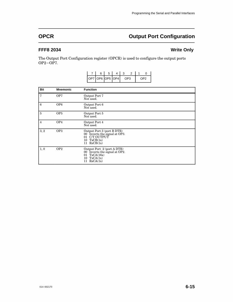
Programming the Serial and Parallel Interfaces
014–002170 6-15
OPCR Output Port Configuration
FFF8 2034 Write Only
�!� �*)&*) �%') �%$�" *'�)"%$ '� "()�' ������ "( *(�� )% �%$�" *'� )!� %*)&*) &%')(
�������
0345
OP5
67
OP4OP6OP7 OP3
2 1
OP2
Bit Mnemonic Function
� ��� �*)&*) �%') �
�%) *(���
� ��� �*)&*) �%') �
�%) *(���
�� �*)&*) �%')
�%) *(���
� ��� �*)&*) �%') �
�%) *(���
�� ��� �*)&*) �%') � �&%') � ����
�� �$+�')( )!� (" $�# �) ����
� ��� ������
� �,���,�
�,���,�
� � �� �*)&*) �%') �&%') � ����
�� �$+�')( )!� (" $�# �) ���
� �,����,�
� �,���,�
�,���,�

Programming the Serial and Parallel Interfaces
014–0021706-16
SRA, SRB Status
FFF8 2004 SRA Read Only
FFF8 2024 SRB
�)& �3"342 1&(*23&12 ����� ���� 01/5*%& 3)& 23"342 /' 5"1*/42 � ��� &11/12 /1
$/.%*3*/.2�
0345
PE
67
OEFEBRK TxE
2
TxRDY
1
FFL RxRDY
Bit Mnemonic Function
� ��� �1&"+
� �/ &11/1�
� �)& $)"..&, 1&$&*5&% ". ",,�9&1/ $)"1"$3&1 6*3)/43 " 23/0 #*3� �.)*#*32
'413)&1 &.31*&2 *.3/ 3)& ���� 4.3*, 3)& �7� ,*.& 1&341.2 3/ 3)& -"1+ 23"3&�
�� �1"-*.( �11/1
� �/ &11/1�
� �)& ,"23 $)"1"$3&1 1&$&*5&% %*% ./3 )"5& " 23/0 #*3�
� �� �"1*38 �11/1
� �/ &11/1�
� �)& ,"23 $)"1"$3&1 1&$&*5&% )"% 3)& *.$/11&$3 0"1*38�
� �� �5&114. �11/1
� �/ &11/1�
� �.& /1 -/1& $)"1"$3&12 *. 3)& 1&$&*5&% %"3" 231&"- 6&1& ,/23�
����� ���� ��� �� ".% �� "1& $,&"1&% #8 61*3*.( �7�� *.3/ 3)&
"001/01*"3& $/--".% 1&(*23&1�
�7� �1".2-*33&1 �-038
� �)& 31".2-*3 1&(*23&1�2� )"5& %"3"� /1 3)& 31".2-*33&1 *2 %*2"#,&%�
� �/3) 3)& 31".2-*3 )/,%*.( 1&(*23&1 ".% 3)& 31".2-*3 2)*'3 1&(*23&1 "1&
&-038�
�7��! �1".2-*33&1 �&"%8
� �)& 31".2-*3 )/,%*.( 1&(*23&1 )"2 %"3"� /1 3)& 31".2-*33&1 *2 %*2"#,&%�
� �)& 31".2-*3 )/,%*.( 1&(*23&1 *2 &-038 ".% 1&"%8 3/ #& ,/"%&% 6*3) "
$)"1"$3&1�
� ��� ���� �4,,
� �)& 1&$&*5& ���� *2 ./3 '4,,� *3 )"2 1//- '/1 -/1& %"3"�
� �)& 1&$&*5& )/,%*.( 1&(*23&1 ������ *2 '4,,�
� �7��! �&$&*5&1 �&"%8
� �)& 1&$&*5& )/,%*.( 1&(*23&1 *2 &-038�
� �)& 1&$&*5& )/,%*.( 1&(*23&1 ������ )"2 1&$&*5&% " $)"1"$3&1 '/1 3)& ��
3/ 1&"%�

Programming the Serial and Parallel Interfaces
014–002170 6-17
Programming the Parallel Interface�*+3 3'%4+0/ '81-#+/3 *07 40 42#/3.+4 # 4*205)* 4*' 1#2#--'- +/4'2(#%'�
PARALLEL Parallel Port
FFF8 A000 Read/Write
�*' 1#2#--'- +/4'2(#%' '/#$-'3 905 40 3'/& 1#2#--'- $94'3 0( # 40 # 12+/4'2� �*' +/4'2(#%'
*#3 # ��$94' $5(('2� 4*'2'(02' 905 %#/ 42#/3.+4 #3 .#/9 #3 %*#2#%4'23 #4 # 4+.'�
!*'/ 3'/&+/) # (+-' 4*#4 '8%''&3 $94'3� 3'/& 4*' (+234 $94'3� 4*'/ 7#+4 (02 #
�2+/4'2 �5(('2 �.149 ����� +/4'22514 $'(02' 3'/&+/) 4*' /'84 $94'3� �*' +/4'2(#%'
)'/'2#4'3 4*' +/4'22514 4*205)* $+4 ����� 0( 4*' �/4'22514 �4#453 ����� 2')+34'2� �0
%-'#2 4*' +/4'22514� 72+4' 40 4*' �-'#2 �/4'22514 �������� 2')+34'2�
7 01234
PRP SEL RDYReserved Res
Bit Mnemonic Function
��� �'3'26'&
� ��� �2+/4'2 �2040%0-
�/&+%#4'3 4*' 12040%0- $'+/) 53'&�
�'/420/+%3�
� /53'&
��� �2+/4'2 �'-'%4
�/&+%#4'3 7*'4*'2 02 /04 4*' 12+/4'2 +3 0/-+/'�
�*' 12+/4'2 +3 0/-+/'�
� �*' 12+/4'2 +3 /04 0/-+/'�
�'3'26'&
� ��" �2+/4'2 �'#&9
�/&+%#4'3 7*'4*'2 02 /04 4*' 12+/4'2 +3 2'#&9 40 12+/4�
�*' 12+/4'2 +3 2'#&9 40 12+/4�
� �*' 12+/4'2 +3 /04 2'#&9 40 12+/4�
Configuring the Parallel Interface�*' 1#2#--'- +/4'2(#%' %#/ %0..5/+%#4' 7+4* # �'/420/+%3�%0.1#4+$-' 12+/4'2� �0 3'-'%4
4*' �'/420/+%3 12040%0-� 3'4 4*' �2+/4'2 �420$' �0-#2+49 $+4 ����� $+4 � 0( 4*' �0/420-
2')+34'2 ����� 40 #3 &'3%2+$'& +/ � :�'.029��
�� ����� 3' %#54+0/ 7*'/ 72+4+/) 40 4*' �0/420- ����� 2')+34'2� %*'%, #-- $+43 (+234�
�/& 0( �*#14'2

Programming the Serial and Parallel Interfaces
014–0021706-18

014–002170 7-1
Chapter 7Programming the PIT, CIO, and
Real–Time Clock
This chapter describes the Zilog Z8536 Counter/Timer and Parallel I/O (CIO) device, theSGS–Thomson MK48T02B 2Kx8 Zeropowert/Timekeepert RAM chip, and theprogrammable interval timer (PIT).
The Real–Time Clock (RTC) and Nonvolatile RAM (NOVRAM) are parts of theSGS–Thomson MK48T02B. The section entitled “Programming the Real–Time Clock(RTC) and Nonvolatile RAM (NOVRAM)” describes the RTC and NOVRAM and how toprogram these devices. For more information on the Real–Time clock and theNOVRAM, see the SGS–Thomson Memory Products Databook.
Each processor has a PIT (Programmable Interval Timer) that it can use to generatetime intervals.
The CIO section describes the programmable CIO registers, how the system board usesthe CIO controller, and how to program the CIO. For more information on the CIO, seethe Z8536 CIO Counter/Timer and Parallel I/O Unit data sheet by Zilog.

Programming the Counter/Timer and the Real–Time Clock
014–0021707-2
Programming the Real–Time Clock (RTC) andNonvolatile RAM (NOVRAM)
The Real–Time Clock (RTC) and Nonvolatile RAM are contained within anSGS–Thomson MK48T02B 2Kx8 Zeropower /Timekeeper RAM chip. The RAM withinthis chip is nonvolatile for over 3 years of operation without power. Real–time clockaccuracy is within 1 minute per month at room temperature (25_C). The device providesa programmable register for calibrating the timekeeper accuracy. In addition to thetimekeeper functions, this chip provides 2040 bytes of NOVRAM used for diagnosticsand system configuration/boot information.
For a detailed description of the Real–Time clock and the NOVRAM, see theSGS–Thomson Memory Products Databook.
Real–Time Clock Registers
The Real–Time Clock (RTC) registers are 8–bit registers in the timekeeper RAM.Software can adjust the RTC by writing the desired time and date to these registers.These registers are realigned on word (32–bit) boundaries and occupy the last eightlocations of the 2048 words reserved for the NOVRAM. Table 7–1 defines the registersand their addresses.
Table 7–1 Real–Time Clock Registers
Register Address Range Format Example
�� ��� ���� ���� # ��
������� ���� ���� ����� ��
���! �� ���� ���� ����� ��
��!� ���� ��� ����� �
��" ���� ���� ���� ��
�� � ���� ���� ����� �
��� � ���� ���� ����� ��
���� ���� ��� ����� ��
The Control register (FFF8 1FE016) allows you to read, set, or calibrate the RTC. Beforereading or writing the RTC registers, you must prevent the clock from updating theregisters by setting the appropriate bit: to read data set bit 6 of the Control register to 1;to write data set bit 7 to 1. Halting the register updating does not affect the Time ofBoot (TOB) clock’s timekeeping. Resetting the read bit to 0 continues updating of theregisters; resetting the write bit to 0 transfers the register values to the RTC andcontinues the timekeeping operations. The date/time values occupy the low–order bits ofthe registers with any unused bits set to 0.
To calibrate the RTC, write a calibration value into bits 0–5 of the Control register. Bit 5is the sign bit: 0 indicates negative calibration, slowing the clock down; 1 indicatespositive calibration, speeding the clock up. Bits 0–4 contain a binary calibration valuefrom 0–31. Each value modifies a number of minutes in each 64–minute cycle of the

Programming the Counter/Timer and the Real–Time Clock
014–002170 7-3
clock. A value of 000012 modifies the first 2 minutes by 1 second per minute. A value of001102 modifies the first 12 minutes by 1 second per minute.
NOVRAM Addresses
The NOVRAM contains 2040 bytes of nonvolatile data for Data General diagnostics andsystem configuration and boot information. The NOVRAM occupies two 4–kilobytepages in the Mbus utility space. Each NOVRAM byte is word aligned in Mbus addressspace, and is accessed as the lowest–order byte (bits 7–0) of each word. Table 7–2defines the NOVRAM addresses.
Table 7–2 NOVRAM Addresses
���� ���� ���
� � � � � � ������� !�� ��� #�� ����� �� ���
���� ��� ����
���� ��� ����
� � � � � � �����"�� �#�� ����� �� ���
���� ���� ����
���� ���� ���
� � � � � � �����"�� ��� #�� ����� �� ���
���� ���� ����
Address NOVRAM Byte Number Comments

Programming the Counter/Timer and the Real–Time Clock
014–0021707-4
Programming the Programmable Interval Timer(PIT)
Each processor has a Programmable Interval Timer (PIT) that it can use to generatetime intervals. This section describes the PIT registers.
PIT_DATA PIT Counter Value
FFC8 4000 PIT_DATA Read/Write
The PIT counter value register (PIT_DATA) initializes the PIT counter. The counter isan up–counter; when the counter overflows bit 23, it sets the P bit in JPIST to 1. Thevalue written to PIT_DATA must be the 2’s complement of the desired time period. Thecounter is clocked at 25 MHz/256 (10.24 µsec per tick).
NOTE: Each job processor (CPU) has its own PIT_DATA register.
NOTE: The counter will continue to count after overflowing bit 23.
Local resets clear PIT_DATA to 0; the counter is disabled because PIT_SC is also reset.
31 16
15 0
PIT_DATA
Unused PIT_DATA
24 23
Bit Mnemonic Function
���� ��" ��
���� � ���� � � ��"�!�� ���"�
���� $��!!��� ���"! !�� ���!��� #��"� �� !�� � � ��"�!���
���� ����� "����� !�� �"����! #��"� �� !�� � � ��"�!���

Programming the Counter/Timer and the Real–Time Clock
014–002170 7-5
PIT_SC PIT Status and Command
FFC8 5000 PIT_SC Read/Write as noted
The PIT Status and Command (PIT_SC) register enables interrupts to a processor.
NOTE: Each processor has its own PIT_SC register.
PIT_SC is reset to 0 by local resets.
31 16
15 012
Unused EN IACK
Unused
Bit Mnemonic Function
�� �!'%��
� � !�� � ��� �"'!&�$ �������$�&��
� !�� � �"'!&�$�
� ��%�� � �"'!&�$�
� ���� � ��$ &�� ��� �!&�$$'#& ��$�&� "! *�
� � ��$ &�� ��� "(�$� ") �!&�$$'#& �! ������
� �" !"& � ��$ ��� "(�$� ") �!&�$$'#&�

Programming the Counter/Timer and the Real–Time Clock
014–0021707-6
Programming the CIOThis section describes the features of the counter/timer and parallel I/O (CIO) device,how it connects to the system board, and to program it.
Features of the CIOThe Zilog Z8536 is a Counter/Timer and Parallel I/O (CIO) device. The CIO containsthree counter/timers, one for each of the three ports, A through C. Each counter/timerconsists of a 16–bit downcounter, a 16–bit Time Constant (TC) register, a 16–bit CurrentCount (CC) register, and two 8–bit registers for control and status. The counter/timersconnect to the outside world through I/O ports. The parallel I/O portion is used only as ameans to pass signals to and from the counter/timers.
Using the CIOThe Zilog Z8536 is a Counter/Timer and Parallel I/O (CIO) device. The CIO containscounter/timers and parallel I/O ports. Figure 7–1 illustrates the CIO, and Table 7–3defines the CIO lines. Figure 7–2 illustrates the counter/timer jumpers to use whenconnecting the counter/timer inputs and outputs.
Jumper P6 to P4
Jumper P8 to P4
PB0PB1PB2PB3PB4PB5PB6PB7
PC0PC1PC2PC3
Z8536CIO
D0D1D2D3D4D5
D6D7
RD*WR*CE*A0A1
PCLKIEIIEO
PA0PA1PA2PA3PA4PA5
PA6PA7
INTACK*INT*
GND+5 V
+5 V
Not used
Not usedNot used
Not used
Not usedNot used
Not used
Not used
Not usedNot used
Not used
Not used
Not usedNot used
Not used
C/T 1 trigger (SI*)C/T 1 gate (BRIRQ1)
C/T 2 output
C/T 1 output
C/T 3 output
C/T 3 input
��������� �� ����� ����� ��
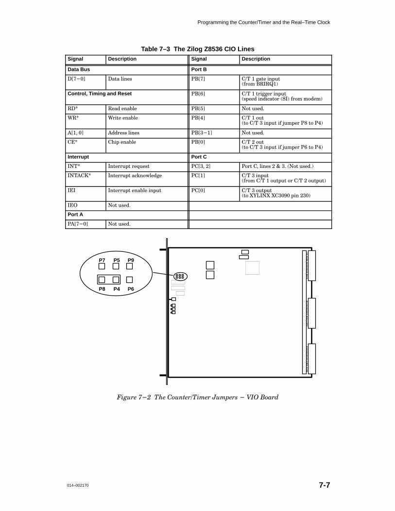
Programming the Counter/Timer and the Real–Time Clock
014–002170 7-7
Table 7–3 The Zilog Z8536 CIO LinesSignal Description Signal Description
Data Bus Port B
�&��' �(;( 305,: ��&�' �" � .(;, 057<;
�-964 � � ���
Control, Timing and Reset ��&�' �" � ;90..,9 057<;
�:7,,+ 05+0*(;69 �!�� -964 46+,4�
�� ,(+ ,5()3, ��&�' �6; <:,+�
# � #90;, ,5()3, ��&�' �" � 6<;
�;6 �" 057<; 0- 1<47,9 �� ;6 ���
�&�� ' �++9,:: 305,: ��& ��' �6; <:,+�
��� �/07 ,5()3, ��&' �" � 6<;
�;6 �" 057<; 0- 1<47,9 �� ;6 ���
Interrupt Port C
��"� �5;,99<7; 9,8<,:; ��& � �' �69; �� 305,: � � � ��6; <:,+��
��"���� �5;,99<7; (*256=3,+., ��&�' �" 057<;
�-964 �" � 6<;7<; 69 �" � 6<;7<;�
��� �5;,99<7; ,5()3, 057<; ��&' �" 6<;7<;
�;6 $%���$ $� � 705 � �
��� �6; <:,+�
Port A
��&��' �6; <:,+�
P8 P4 P6
P7 P5 P9
���������� ��� ������������� ������ � � �����

Programming the Counter/Timer and the Real–Time Clock
014–0021707-8
Programming the Counter/TimersTo use the CIO as a counter/timer, a programmer must set–up and start thecounter/timer, then wait for an interrupt from the CIO indicating that the countdownhas reached zero.
The CIO has programmable registers used to control the CIO and obtain status from theCIO. Table 7–4 identifies the CIO registers and their 6–bit pointers.
Table 7–4 CIO Registers
Register Pointer Register Pointer
Master Control Registers Port Specification Registers
�#34'2 �/4'22514 �0/420- �� �024 �0&' �1'%+(+%#4+0/ � �
�#34'2 �0/(+)52#4+0/ �0/420- � �024 �0&' �1'%+(+%#4+0/ � �
Counter/Timer Registers �024 �#/&3*#,' �1'%+(+%#4+0/ �
�05/4'2� +.'2 �0..#/& � �4#453 �� �024 �#/&3*#,' �1'%+(+%#4+0/ � �
�05/4'2� +.'2 �0..#/& � �4#453 �� �024 �0..#/& #/& �4#453 � ��
�05/4'2� +.'2 � �0..#/& � �4#453 �� �024 �0..#/& #/& �4#453 � ��
�05/4'2� +.'2 �0&' �1'%+(+%#4+0/ � Bit Path Definition Registers
�05/4'2� +.'2 �0&' �1'%+(+%#4+0/ � �#4# �#4* �0-#2+47 �
�05/4'2� +.'2 � �0&' �1'%+(+%#4+0/ � �#4# �#4* �0-#2+47 � �
�05/4'2� +.'2 �522'/4 �05/4 ����� � �#4# �#4* �0-#2+47 � �
�05/4'2� +.'2 �522'/4 �05/4 ����� �#4# �+2'%4+0/ � �
�05/4'2� +.'2 �522'/4 �05/4 ����� �#4# �+2'%4+0/ � �
�05/4'2� +.'2 �522'/4 �05/4 ����� � �#4# �+2'%4+0/ � ��
�05/4'2� +.'2 � �522'/4 �05/4 ����� � �1'%+#- ��� �0/420- � �
�05/4'2� +.'2 � �522'/4 �05/4 ����� �1'%+#- ��� �0/420- � �
�05/4'2� +.'2 +.' �0/34#/4 ����� � �1'%+#- ��� �0/420- � ��
�05/4'2� +.'2 +.' �0/34#/4 ����� � Port Data Registers
�05/4'2� +.'2 +.' �0/34#/4 ����� � �024 � �#4# ��
�05/4'2� +.'2 +.' �0/34#/4 ����� � �024 � �#4# ��
�05/4'2� +.'2 � +.' �0/34#/4 ����� � �024 � �#4# ��
�05/4'2� +.'2 � +.' �0/34#/4 ����� � Pattern Definition Registers
Interrupt Vector Registers �#44'2/ �0-#2+47 �
�/4'22514 !'%402 �')+34'2 � � �#44'2/ �0-#2+47 � �
�/4'22514 !'%402 �')+34'2 � �� �#44'2/ 2#/3+4+0/ � �
�/4'22514 !'%402 �')+34'2 �� �� �#44'2/ 2#/3+4+0/ � �
�522'/4 !'%402 �')+34'2 � �#44'2/ �#3, � �
�#44'2/ �#3, � �
Access the control registers as follows:
� "2+4' 4*' ��$+4 10+/4'2 40 4*' 4#2)'4 2')+34'2 +/40 4*' 10+/4'2 2')+34'2 -0%#4'& #4
#&&2'33 ���� �����
� �'#& (20. 02 62+4' 40 4*' 4#2)'4 2')+34'2�

Programming the Counter/Timer and the Real–Time Clock
014–002170 7-9
When a countdown reaches zero, the CIO sets the Interrupt Pending (IP) bit in theappropriate Counter/Timer Command and Status (CTCS) register and asserts the INT*line. The system board interrupt logic processes this interrupt signal and sets the CIOInterrupt bit (CIO) in the Interrupt Status (IST) register. If another countdown reacheszero while a CIO interrupt is still pending (i.e. the IP bit is set) the CIO sets an internalerror flag. When the pending interrupt completes, the error flag forces both the IP bitand the Interrupt Error (ERR) bit set. Figure 7–3 illustrates how the CIOcounter/timers are configured.
Output
Output
InputC/T 3
C/T 2
C/T 1
Interrupt logic
When the C/T 3 output goes High, itsets the CIO Interrupt (CIO) bit of theInterrupt Status (IST) register.
IST register
Trigger (SI*)
Gate (BRIRQ1)
Output
�������� �� ��������� ��

Programming the Counter/Timer and the Real–Time Clock
014–0021707-10
CIO RegistersThis section describes the CIO registers. The types of CIO registers include mastercontrol registers, counter/timer registers, interrupt vector registers, port specificationregisters, port data registers, and pattern definition registers.
Master Control RegistersThis section describes the master control registers: Master Interrupt Control (MIC) andMaster Configuration Control (MCC).
MIC Master Interrupt Control
Pointer 00 Read/Write
The Master Interrupt Control (MIC) register defines what type of interrupt request ispending. The interrupt vector is located in the Current Vector (CV) register. The MICregister also enables or disables the interrupt output line (INT*).
7 6 5 01234
PBV CTV RJA RESETPAVNVDLCMIE
Bit Mnemonic Function
� ��� �!23%1 �-3%114/3 �-!"+%
�-!"+%2 !-$ $)2!"+%2 !++ ��� )-3%114/3 1%04%232 "7 $)2!"+)-' 3(% ���� +)-%�
��� )-3%114/3 1%04%232 !1% %-!"+%$ .1 $)2!"+%$ "7 3(%)1 1%2/%#3)5%
)-3%114/3 %-!"+% ")32�
� ��� )-3%114/3 1%04%232 !1% $)2!"+%$� ��� .5%11)$%2 !++ )-$)5)$4!+
)-3%114/3 %-!"+% ")32�
� ��� �)2!"+% �.6%1 �(!)-
�.3 42%$�
�� �. �%#3.1
�-!"+%2 !-$ $)2!"+%2 3(% .43/43 .& )-3%114/3 5%#3.12 6(%- 1%!$ "7 !-
)-3%114/3 2%15)#% 1.43)-%�
�)2!"+%2 3(% .43/43 .& !- )-3%114/3 5%#3.1 6(%- 1%!$�
� �-!"+%2 3(% .43/43 .& !- )-3%114/3 5%#3.1 6(%- 1%!$�
� ��� �.13 � �%#3.1 �-!"+%
�.3 42%$�
� ��� �.13 � �%#3.1 �-!"+%
�-!"+%2 !-$ $)2!"+%2 3(% /.13 � )-3%114/3 5%#3.1�
�-!"+%2 3(% /.13 � )-3%114/3 5%#3.1�
� �)2!"+%2 3(% /.13 � )-3%114/3 5%#3.1�
��� �.4-3%1��),%1 �%#3.1 �-!"+%
�-!"+%2 !-$ $)2!"+%2 3(% #.4-3%1�3),%1 )-3%114/3 5%#3.1�
�-!"+%2 3(% #.4-3%1�3),%1 )-3%114/3 5%#3.1�
� �)2!"+%2 3(% #.4-3%1�3),%1 )-3%114/3 5%#3.1�
��� �)'(3 �423)&)%$ �$$1%22
�423)&)%2 3(% !$$1%22 6)3( %)3(%1 �� .1 ��
�)'(3 *423)&7 ��� )2 +.!$%$ &1., �����
� �()&3 +%&3 .-% ")3 ��� )2 +.!$%$ &1., ����
� ����� �%2%3
(%- ����� )2 2%3 3. � 3(% ��� 1%2%32�

Programming the Counter/Timer and the Real–Time Clock
014–002170 7-11
MCC Master Configuration Control
Pointer 01 Read/Write
The Master Configuration Control (MCC) register enables or disables the ports andtimers.
7 6 5 01234
PLC PAE LCCT3ECT2ECT1EPBE
Bit Mnemonic Function
��� �$&( � �#��!�
�#��!�' �#� ��'��!�' %$&( ��
� �#��!�' %$&( ��
� ��'��!�' %$&( ��
� ���� �$)#(�&���"�& � �#��!�
�#��!�' �#� ��'��!�' �$)#(�&�(�"�& ��
� �#��!�' �$)#(�&�(�"�& ��
� ��'��!�' �$)#(�&�(�"�& ��
� ���� �$)#(�&���"�& � �#��!�
�#��!�' �#� ��'��!�' �$)#(�&�(�"�& ��
� �#��!�' �$)#(�&�(�"�& ��
� ��'��!�' �$)#(�&�(�"�& ��
��� �$)#(�&���"�& �#� �$&( � �#��!�
�#��!�' �#� ��'��!�' �$)#(�&�(�"�& �#� %$&( ��
� �#��!�' �$)#(�&�(�"�& �#� %$&( ��
� ��'��!�' �$)#(�&�(�"�& �#� %$&( ��
��� �$&( ��# �$#(&$!
��# ' %$&(' � �#� ��
� �$&(' � �#� � �&� !�# ���
� �$&(' � �#� � $%�&�(� �#��%�#��#(!*�
��� �� ��� ���� �� ��� �� �����
� ��� �$&( � �#��!�
��� �� ��� ��� �� �����
�� � ����� �� �$)#(�&���"�& ��# �$#(&$!'
��# ' (�� �$)#(�&�(�"�& � $)(%)( ($ �$)#(�&�(�"�& ��
LC[1] LC[0] Function� � ��� ���' �&� �#��%�#��#(�
� � ��� ��' $)(%)( ��(�' ��� ��
� � ��� ��' $)(%)( (&����&' ��� ��
� � ��� ��' $)(%)( �' ��� ��' �$)#( �#%)(�

Programming the Counter/Timer and the Real–Time Clock
014–0021707-12
Counter/Timer RegistersThis section describes the Counter/Timer registers.
CTCS Counter/Timer Command and Status
Pointer 0A C/T 1 Read/Partial Write
Pointer 0B C/T 2
Pointer 0C C/T 3
The Counter/Timer Command and Status (CTCS) registers indicate the status of thecounter/timers and pass commands to the counter/timers. Each counter/timer has anassociated CTCS register with a pointer as shown above.
7 6 5 01234
RCC GCB TCBIPIEIUS ERR CIP
Bit Mnemonic Function
� ��� �)/!--0+/ �) !- �!-1%�! ��!� *)'3�
�) %��/!. 2$!/$!- *- )*/ /$! �)/!--0+/ �!) %)# ���� %)/!--0+/ %. �!%)#
.!-1%�! �
�$! �� %)/!--0+/ %. �!%)# .!-1%�! �
� �$! �� %)/!--0+/ %. )*/ �!%)# .!-1%�! �
�� �)/!--0+/ �)��'! ��!� ��-%/!�
�)��'!. *- (�.&. /$! �)/!--0+/ �!) %)# ���� %)/!--0+/�
�)��'!. /$! �� %)/!--0+/� �$!) �� %. .!/� /$! ���� '%)! /* /$! ��� -!#%./!-
*" /$! .3./!( �*�- 2%'' �! �..!-/! �
� ��.&. /$! �� %)/!--0+/� �$! �� �%/ (�3 �! .!/� �0/ /$! ���� '%)! /* /$!
��� -!#%./!- 2%'' )*/ �! �..!-/! �
� �� �)/!--0+/ �!) %)# ��!� *)'3�
�� %. .!/ 2$!) �) !1!)/ -!,0%-%)# %)/!--0+/ .!-1%�%)# *��0-.� �$!) �� %. .!/�
/$! ��� -%1!. /$! ���� '%)! �*2� �$!) -!� � �� %) %��/!. 2$!/$!- *- )*/ �)
%)/!--0+/ %. +!) %)#�
�$! �*0)/!- $�. -!��$! %/. /!-(%)�' �*0)/� �) /$! %)/!--0+/ %. +!) %)#�
� �* %)/!--0+/ %. +!) %)# "*- /$%. �*0)/!-�/%(!-�
� ��� �)/!--0+/ �--*- ��!� *)'3�
�) %��/!. /$�/ �) %)/!--0+/ *��0--! 2$%'! � +-!1%*0. %)/!--0+/ 2�. ./%''
+!) %)#�
�) %��/!. /$�/ �) %)/!--0+/ !--*- $�. *��0--! � %�!� �) %)/!--0+/ *��0--!
2$%'! � +-!1%*0. %)/!--0+/ 2�. ./%'' +!) %)#�
� �* %)/!--0+/ %. +!) %)# "*- /$%. �*0)/!-�/%(!-�
��� �!� �*0)/!- �*)/-*' ��-%/! *)'3�
��� ��) �! .!/ *)'3� �$!) .!/� ��� "-!!4!. /$! 1�'0!.* /$�/ /$! ��� ��)
-!� /$! �*0)/!-�/%(!- �) #!/ � 1�'% �*0)/� �$!) /$! ��� -!� . /$!
�*0)/!-�/%(!-� ��� %. �'!�-! �) /$! �*0)/!-�/%(!- �*0)/ *2) -!.0(!.�
��*)/%)0! �

Programming the Counter/Timer and the Real–Time Clock
014–002170 7-13
Bit Mnemonic Function
��� ��(� �#!!�"� ��( �������&�(��
�"�� �' �"� ��'�� �' (�� #)($)( #� �"(�&&)$( &�%)�'(' �&#! (�� ����
� �"�� �' �"(�&&)$( &�%)�'('�
� �'�� �' �"(�&&)$( &�%)�'('�
���� ��� ��(� �#!!�"� ��( !)'( �� '�( �#& (�� ��� (# ��"�&�(�
�"(�&&)$('�
� ��� �&����& �#!!�"� ��( ��&�(� #" +�
�&�(�"� � � (# ��� #��' (�� �#*"�#)"(�&�
� ��� �#)"( �" �&#�&�'' ����� #" +�
�"����(�' *��(��& #& "#( (�� �#)"(�& �' �#)"(�"� �#*"�
� ��� �#*"�#)"(�& ��' ���" #����� �"� (�� �#)"(�#*" ��' "#( &������
,�&#�
� ��� �#*"�#)"(�& ��' &������ ,�&#�
��#"� )����

Programming the Counter/Timer and the Real–Time Clock
014–0021707-14
CTMS Counter/Timer Mode Specification
Pointer 1B C/T 1 Read/Write
Pointer 1C C/T 2
Pointer 1D C/T 3
The Counter/Timer Mode Specification (CTMS) registers set various Counter/Timerparameters such as the method for triggering the counter/timer, the countdown rate, andwhether or not the counter output is enabled.
7 6 5 01234
EGE REB DCSECEEOEC/SC ETE
Bit Mnemonic Function
� ����� �,+1(+2,20��(+&)$� �6")$
�,+1/,)0 1'$ ,-$/ 1(,+ ,% 1'$ ",2+1$/ 4'$+ 1'$ ",2+1 /$ "'$0 7$/,�
� �,+1(+2,20 "6")$� �'$+ 1'$ ",2+1 /$ "'$0 7$/,� 1'$ 1(*$ ",+01 +1 (0
/$), #$# +# 1'$ ",2+1#,4+ /$02*$0�
� �(+&)$ "6")$� �'$+ 1'$ ",2+1 /$ "'$0 7$/,� 1'$ ",2+1#,4+ 0$.2$+"$ 01,-0�
��� �51$/+ ) �21-21 �+ !)$
�+ !)$0 +# #(0 !)$0 1'$ $51$/+ ) ,21-21 %/,* 1'$ /$0-$"1(3$ ",2+1$/�1(*$/�
� �+ !)$0 1'$ $51$/+ ) ,21-21�
� �(0 !)$0 1'$ $51$/+ ) ,21-21�
� ��� �51$/+ ) �,2+1 �+ !)$
�'$+ 1'$ #,4+",2+1$/ 20$0 1'$ �(*$/ *,#$ 1, ",2+1 #,4+� 1'$ ��� !(1
#$1$/*(+$0 1'$ / 1$ ,% 1'$ ",2+1 #,4+�
� �'$ #,4+",2+1$/ ",2+10 #,4+ 1 1'$ ���� %/$.2$+"6�
� �'$ #,4+",2+1$/ ",2+10 #,4+ 1 ' )% 1'$ ���� %/$.2$+"6�
� ��� �51$/+ ) �/(&&$/ �+ !)$
�+ !)$0 +# #(0 !)$0 1'$ $51$/+ ) 1/(&&$/ (+-21 1, 1'$ /$0-$"1(3$ ",2+1$/�1(*$/�
� �+ !)$0 1'$ $51$/+ ) 1/(&&$/�
� �(0 !)$0 1'$ $51$/+ ) 1/(&&$/�
����� ��� (0 20$# %,/ ��� � ,+)6� ��� +# ��� #, +,1 20$ ����
��� �51$/+ ) � 1$ �+ !)$
�+ !)$0 +# #(0 !)$0 1'$ $51$/+ ) & 1$ (+-21 1, 1'$ /$0-$"1(3$ ",2+1$/�1(*$/�
� �+ !)$0 1'$ $51$/+ ) & 1$�
� �(0 !)$0 1'$ $51$/+ ) & 1$�
����� � � ���� �� ��� �� ��� ��� �� � ��� �� �� � �� ���� ��� ��
� �����
��� �$1/(&&$/ �+ !)$ �(1
�$%(+$0 4'$1'$/ ,/ +,1 1'$ ",2+1$/�1(*$/ /$ "10 1, 1/(&&$/0 (+(1( 1$# 4'()$ 1'$
",2+1$/ (0 ",2+1(+& #,4+� �% ��� (0 0$1� 1'$ ",//$0-,+#(+& ",2+1$/�1(*$/
/$), #0 1'$ #,4+",2+1$/ +# /$01 /10 1'$ ",2+1#,4+ 0$.2$+"$�
� �$), # +# /$01 /1 1'$ ",2+1$/�1(*$/ 4'$+ 1/(&&$/$#�
� �, +,1 /$0-,+# 1, 1/(&&$/0�
�� � ��� �21-21 �216 �6")$
�$)$"10 + ,21-21 0(&+ ) *,#$ %,/ 1'$ ",2+1$/�1(*$/ 0 %,)),40�
DCS[1] DCS[0] Function� � �2)0$ ,21-21
� � �+$�0',1 ,21-21
� � �.2 /$�4 3$ ,21-21
� � �, +,1 0-$"(%6 ,21-21

Programming the Counter/Timer and the Real–Time Clock
014–002170 7-15
CTCC Counter/Timer Current Count
Pointer 10 C/T 1, MSB Read only
Pointer 11 C/T 1, LSB
Pointer 12 C/T 2, MSB
Pointer 13 C/T 2, LSB
Pointer 14 C/T 3, MSB
Pointer 15 C/T 3, LSB
The Counter/Timer Current Count (CTCC) registers contain the current value of theirrespective downcounter. To accurately read a CTCC register, the related counter/timermust be stopped. Each counter/timer has an associated CTCC register with a pointer asshown above.
CTCC Most–Significant Byte (MSB) Registers
The CTCC MSB registers contain the most–significant byte of the 16–bit current count.
CTCC–MSB
15 8
Bit Mnemonic Function
��� ��� ��� ����������� �$ �
�� ���� �� �!���� ��!� ��#� "��!� �� �� ��� ����������� �$ � ����� ��
�� ������� �� ��!� ��� �����
CTCC Least–Significant Byte (LSB) Registers
The CTCC LSB registers contain the least–significant byte of the 16–bit current count.
7 0
CTCC–LSB
Bit Mnemonic Function
�� ��� ���� ����������� �$ �
�� ���� �� �!���� ��!� ��#� "��!� �� �� ���� ����������� �$ � ����� ��
�� ������� �� ��!� ��� �����

Programming the Counter/Timer and the Real–Time Clock
014–0021707-16
CTTC Counter/Timer Time Constant
Pointer 16 C/T 1, MSB Read/Write
Pointer 17 C/T 1, LSB
Pointer 18 C/T 2, MSB
Pointer 19 C/T 2, LSB
Pointer 1A C/T 3, MSB
Pointer 1B C/T 3, LSB
The Counter/Timer Time Constant (CTTC) registers contain the 16–bit time constantsused by their respective counter/timers as an initial value when counting down to zero.Each counter/timer has an associated CTTC register with a pointer as shown above.
CTTC Most–Significant Byte (MSB) Registers
The CTTC MSB registers contain the most–significant byte of the 16–bit time constant.
CTTC–MSB
15 8
Bit Mnemonic Function
��� ��� ��� ����������� �# �
�� ���� �� ��� ����������� �# � ����� �� �� ��� ��� ��� ���� �� ����
"���� �� ��!� ��� ���� "��� ��!� ��"��
CTTC Least–Significant Byte (LSB) Registers
The CTTC LSB registers contain the least–significant byte of the 16–bit time constant.
7 0
CTTC–LSB
Bit Mnemonic Function
�� ��� ���� ����������� �# �
�� ���� �� ���� ����������� �# � ����� �� �� ��� ��� ��� ���� �� ����
"���� �� ��!� ��� ���� "��� ��!� ��"��

Programming the Counter/Timer and the Real–Time Clock
014–002170 7-17
Interrupt Vector RegistersThis section describes the interrupt vector registers.
IV Interrupt Vector
Pointer 02 Port A (not used) Read/Write
Pointer 03 Port B
Pointer 04 Counter/Timers
The Interrupt Vector (IV) registers contain the vector(s) for interrupt service routines.The CIO interrupt service routine reads the IV register to access the appropriatesecondary interrupt service routine (ISR).
7 0
IV
Bit Mnemonic Function
��� � ��������� �����
������� ��� ��������� ������ �� ��� ��� ��������� ������� �������� ��� ���
�� �������� ��� ��������� �� ������� �� �� ��� � ����

Programming the Counter/Timer and the Real–Time Clock
014–0021707-18
CV Current Vector
Pointer 1F Read only
The Current Vector (CV) register contains the interrupt vector for the current CIOinterrupt request with the highest priority. The primary interrupt service routineexecutes the secondary interrupt service routine located at this vector.
7 0
CV
Bit Mnemonic Function
��� � ���� �� ����
� �������� �� ��� ����� � ���� ��� �� � �� �� ��� ����� � �� �� ��
� ��� � �� �� �� �� ��� ����� ���� �� ���� �� ���������
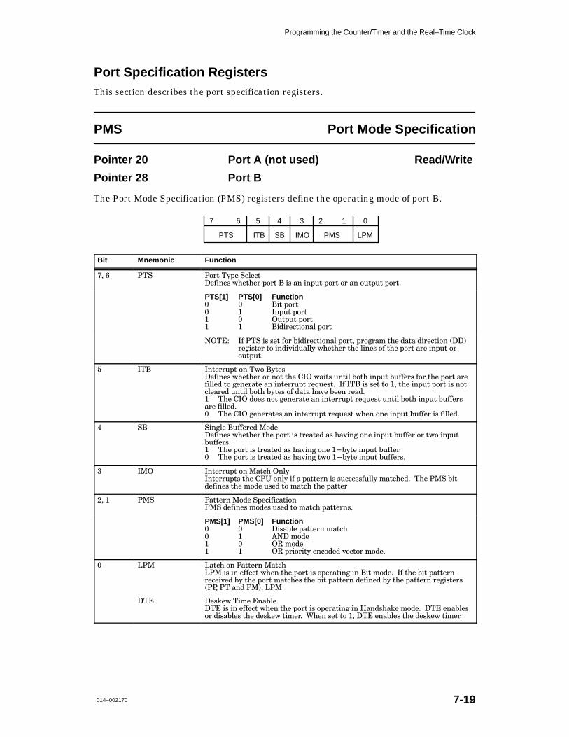
Programming the Counter/Timer and the Real–Time Clock
014–002170 7-19
Port Specification RegistersThis section describes the port specification registers.
PMS Port Mode Specification
Pointer 20 Port A (not used) Read/Write
Pointer 28 Port B
The Port Mode Specification (PMS) registers define the operating mode of port B.
7 6 5 01234
IMO PMS LPMSBITBPTS
Bit Mnemonic Function
�� ��� �.13 �7/% �%+%#3
�%&)-%2 6(%3(%1 /.13 � )2 !- )-/43 /.13 .1 !- .43/43 /.13�
PTS[1] PTS[0] Function� � �)3 /.13
� � �-/43 /.13
� � �43/43 /.13
� � �)$)1%#3).-!+ /.13
����� �& ��� )2 2%3 &.1 ")$)1%#3).-!+ /.13� /1.'1!, 3(% $!3! $)1%#3).- ����
1%')23%1 3. )-$)5)$4!++7 6(%3(%1 3(% +)-%2 .& 3(% /.13 !1% )-/43 .1
.43/43�
� ��� �-3%114/3 .- �6. �73%2
�%&)-%2 6(%3(%1 .1 -.3 3(% ��� 6!)32 4-3)+ ".3( )-/43 "4&&%12 &.1 3(% /.13 !1%
&)++%$ 3. '%-%1!3% !- )-3%114/3 1%04%23� �& ��� )2 2%3 3. �� 3(% )-/43 /.13 )2 -.3
#+%!1%$ 4-3)+ ".3( "73%2 .& $!3! (!5% "%%- 1%!$�
� �(% ��� $.%2 -.3 '%-%1!3% !- )-3%114/3 1%04%23 4-3)+ ".3( )-/43 "4&&%12
!1% &)++%$�
� �(% ��� '%-%1!3%2 !- )-3%114/3 1%04%23 6(%- .-% )-/43 "4&&%1 )2 &)++%$�
� �� �)-'+% �4&&%1%$ �.$%
�%&)-%2 6(%3(%1 3(% /.13 )2 31%!3%$ !2 (!5)-' .-% )-/43 "4&&%1 .1 36. )-/43
"4&&%12�
� �(% /.13 )2 31%!3%$ !2 (!5)-' .-% ��"73% )-/43 "4&&%1�
� �(% /.13 )2 31%!3%$ !2 (!5)-' 36. ��"73% )-/43 "4&&%12�
��� �-3%114/3 .- �!3#( �-+7
�-3%114/32 3(% ��� .-+7 )& ! /!33%1- )2 24##%22&4++7 ,!3#(%$� �(% ��� ")3
$%&)-%2 3(% ,.$% 42%$ 3. ,!3#( 3(% /!33%1
� � ��� �!33%1- �.$% �/%#)&)#!3).-
��� $%&)-%2 ,.$%2 42%$ 3. ,!3#( /!33%1-2�
PMS[1] PMS[0] Function� � �)2!"+% /!33%1- ,!3#(
� � ��� ,.$%
� � �� ,.$%
� � �� /1).1)37 %-#.$%$ 5%#3.1 ,.$%�
� ��� �!3#( .- �!33%1- �!3#(
��� )2 )- %&&%#3 6(%- 3(% /.13 )2 ./%1!3)-' )- �)3 ,.$%� �& 3(% ")3 /!33%1-
1%#%)5%$ "7 3(% /.13 ,!3#(%2 3(% ")3 /!33%1- $%&)-%$ "7 3(% /!33%1- 1%')23%12
���� �� !-$ ���� ���
��� �%2*%6 �),% �-!"+%
��� )2 )- %&&%#3 6(%- 3(% /.13 )2 ./%1!3)-' )- �!-$2(!*% ,.$%� ��� %-!"+%2
.1 $)2!"+%2 3(% $%2*%6 3),%1� (%- 2%3 3. �� ��� %-!"+%2 3(% $%2*%6 3),%1�

Programming the Counter/Timer and the Real–Time Clock
014–0021707-20
PHS Port Handshake Specification
Pointer 21 Port A (not used) Read/Write
Pointer 29 Port B
The Port Handshake and Specification (PHS) registers define the type of handshakingused by ports A and B.
7 6 5 023
DTSRWSHTS
Bit Mnemonic Function
� � ��� ��(�-#�% �1* �* �$!$��.$)(
� .# ���� �� ������������� ��� ������� �� ���� ��.� -# . �1 �$&)"�
HTS[1] HTS[0] Function� � �(. ,&)�% � #�(�-#�%
� � �.,)� � #�(�-#�%
� � �/&- � #�(�-#�%
� � �#, �0$, #�(�-#�%
�� ��� ������������� �* �$!$��.$)(
� .# ���� �� ������������� ��� ������� �� ���� ��.� -# . �1 �$&)"�
HTS[2] HTS[1] HTS[0] Function� � � ������������� �$-��& �
� � � �/.*/. �����
� � � �(*/. �����
� � � �* �$�& , +/ -.
� � � �/.*/. , +/ -.
� � � �(*/. , +/ -.
�� ��� � -% 0 �$' �* �$!$��.$)(
� .# ���� �� ������������� ��� ������� �� ���� ��.� -# . �1 �$&)"�

Programming the Counter/Timer and the Real–Time Clock
014–002170 7-21
PCS Port Command and Status
Pointer 08 Port A (not used) Read/Partial Write
Pointer 09 Port B
The Port Command and Status (PCS) registers provide status–information–for andcontrol–of ports A and B.
7 6 5 01234
ORE IRF PMFIPIEIUS ERR IOE
Bit Mnemonic Function
� ��� �+1#//2-1 �+"#/ �#/3'!#
�+"'!�1#0 1&�1 1&# '+1#//2-1 /#.2#01 '0 #'+% 0#/3'!#" �+" '0 +,1 !,*-)#1#"�
��� '0 15-'!�))5 20#" 4'1&'+ � "�'05 !&�'+ ,$ 14, ,/ *,/# '+1#//2-1'+% "#3'!#0
1, -/#3#+1 ),4#/�-/',/'15 "#3'!#0 $/,* %#+#/�1'+% �+ '+1#//2-1 /#.2#01 4&')#
�+ '+1#//2-1 $/,* 1&# "#3'!# 4'1& &'%&#/ -/',/'15 '0 #'+% &�+")#"� �&'0
$#�12/# '0 +,1 20#" '+ 1&'0 0501#* #!�20# 1&# ��� '0 +,1 !,+$'%2/#" 4'1&'+ �+
'+1#//2-1 "�'05 !&�'+�
� ��� '+1#//2-1 /#.2#01 '0 #'+% 0#/3'!#"�
� �&# ��� '0 +,1 0#/3'!'+% �+5 ��� '+1#//2-1�
� �� �+1#//2-1 �+� )#
�+� )#0 ,/ *�0(0 -,/1 � '+1#//2-1 /#.2#010�
�,/1 � '+1#//2-1 /#.2#010 �/# #+� )#"�
� �,/1 � '+1#//2-1 /#.2#010 �/# *�0(#"�
�� �+1#//2-1 �#+"'+%
�+"'!�1#0 1&�1 �+ '+1#//2-1 /#.2#01 '0 -#+"'+%� �&#+ �� '0 0#1� 1&# ��� �00#/10
1&# ���� )'+# 4&'!&� 1&/,2%& '+1#//2-1 ),%'! ,+ 1&# 0501#* ,�/"� 0#10 1&# ���
�+1#//2-1 ����� '1 '+ 1&# �+1#//2-1 �1�120 ����� /#%'01#/�
�+ '+1#//2-1 /#.2#01 '0 -#+"'+%�
� �, '+1#//2-1 /#.2#010 �/# -#+"'+%�
� ��� �+1#//2-1 �//,/ ��#�" ,+)5�
�&#+ 0#1� ��� '+"'!�1#0 1&�1 �+ '+1#//2-1 #//,/ ,!!2/#"�
� ��� �21-21 �#%'01#/ �*-15 ��#�" ,+)5�
�&#+ 0#1� ��� '+"'!�1#0 1&�1 ,21-21 /#%'01#/ � 2$$#/� '0 #*-15�
��� �+-21 �#%'01#/ �2)) ��#�" ,+)5�
�&#+ 0#1� ��� '+"'!�1#0 1&�1 1&# '+-21 /#%'01#/ � 2$$#/� '0 $2))�
��� ��11#/+ ��1!& �)�% ��#�" ,+)5�
�&#+ 0#1� ��� '+"'!�1#0 1&�1 1&# -�11#/+ &�0 ##+ *�1!&#"�
� ��� �+1#//2-1 �+ �//,/
�## 1&# ���� �� ������������� ��� ������� �� ���� "�1� 0&##1 5 �'),%�
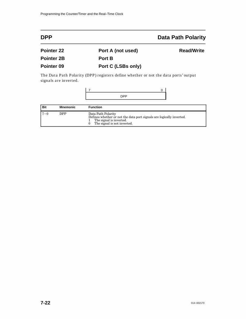
Programming the Counter/Timer and the Real–Time Clock
014–0021707-22
DPP Data Path Polarity
Pointer 22 Port A (not used) Read/Write
Pointer 2B Port B
Pointer 09 Port C (LSBs only)
The Data Path Polarity (DPP) registers define whether or not the data ports’ outputsignals are inverted.
7 0
DPP
Bit Mnemonic Function
��� ��� �� ��� �������
� ��� � �� �� � �� ��� �� �� ���� ������ � �������� ��� �� ��
� � ����� �� ��� �� ��
� � ����� �� ��� ��� �� ��

Programming the Counter/Timer and the Real–Time Clock
014–002170 7-23
DD Data Direction
Pointer 23 Port A (not used) Read/Write
Pointer 2C Port B
Pointer 06 Port C
The Data Direction (DD) register defines the direction (receive or transmit) of each lineof the data ports A, B and C.
7 0
DD
Bit Mnemonic Function
��� ��� ��� ����
������ ��� ���� ���� ������ �� ������� �� �� � ���� �� ��� ���� �����
� �����
� �������

Programming the Counter/Timer and the Real–Time Clock
014–0021707-24
SIO Special I/O Control
Pointer 24 Port A (not used) Read/Write
Pointer 2C Port B
Pointer 07 Port C
The Special I/O Control (SIO) registers define how the I/O is electrically configured.
7 0
SIO
Bit Mnemonic Function
�� ��� ������� ��� �� ���
������� "�� ��� �� �� �� ���! �� � ��� ������!��� �� � ��� �� ����� ���
"�� ��� �� �! �! � ��� ������!��� �� ���� ������
� �! �! "� � ���� ������ �� ���! "� � ��� �� �����
� ����� ���! �� �! �! �

Programming the Counter/Timer and the Real–Time Clock
014–002170 7-25
Port Data RegistersThis section describes the Port Data registers.
PD Port Data
Pointer 0D Port A (not used) Read/Write
Pointer 0E Port B
The Port Data (PD) register passes data to and from the corresponding port A or port B.The PD register consists of three registers: the input data register, the output dataregister, and the buffer register. These registers temporarily store data that wasreceived by or that will be transmitted through the corresponding port.
7 0
PD
Bit Mnemonic Function
��� �� ���� ��
��� �� � �� ������� ��� �������� �� ��� ����� � ��������� ��� ��������
�� ������ ��� � �� ��� ������ � �������� �� �� ���� ������� ���
��������� ��� �����

Programming the Counter/Timer and the Real–Time Clock
014–0021707-26
PCD Port C Data
Pointer 0F Read/Write
The Port C Data (PCD) register passes data to and from port C. The PCD registerconsists of two registers: the input data register and the output data register. Theseregisters temporarily store data that was received by or that will be transmitted throughport C.
7 0
PCDPCDE
34
Bit Mnemonic Function
�� � �� �!#% ��%�
���$� ��%$ � ���� � � ��$� ��%$ ���� ��% � � ����$ !# ��$�$ ��% �� ��%
�����%$ ��% �� � � $! ! �
� ��$�$ %�� �!##�$"! �� � ��%�
� � ����$ %�� �!##�$"! �� � ��%�
��� � � �!#% ��%�
��� #���� � � #�%&# $ %�� �! %� %$ !� �%$ � "&% ��%� #���$%�#� ��� '#�%%� �
� � $%!#�$ %�� ��%� � %�� !&%"&% ��%� #���$%�# %! �� $� % %�#!&�� "!#% �

Programming the Counter/Timer and the Real–Time Clock
014–002170 7-27
Pattern Definition RegistersThis section describes the pattern definitions registers.
PP Pattern Polarity
Pointer 25 Port A (not used) Read/Write
Pointer 2D Port B
The Pattern Polarity (PP) registers define the patterns that will generate interrupts.
7 0
PP
Bit Mnemonic Function
��� ������ �������
������� ��� �������� �� ��� ������� ���� ���� �������� �� ��������� ����
������ �
� ���
� ���

Programming the Counter/Timer and the Real–Time Clock
014–0021707-28
PT Pattern Transition
Pointer 26 Port A (not used) Read/Write
Pointer 2E Port B
The Pattern Transition (PT) registers define whether or not the patterns are detected asa transition from one state to another (i.e. 1 to 0, or 0 to 1) or as a steady state (0 or 1).The state or transition of each bit is defined by the Pattern Polarity (PP) register.
7 0
PT
Bit Mnemonic Function
��� � ������� ���������
������� ������� ��� �������� ��� ������ �� � ���� � ����� �� �� � �����������
� ���������
� ��� � �����

Programming the Counter/Timer and the Real–Time Clock
014–002170 7-29
PM Pattern Mask
Pointer 27 Port A (not used) Read/Write
Pointer 2F Port B
The Pattern Mask (PM) registers mask or enable the pattern bits of the correspondingPattern Polarity (PP) registers.
7 0
PM
Bit Mnemonic Function
��� �� � ����� � ��
� ��� �� �� ���� � �� � ����� ��� �� ��� � ����� ��� ���� ���� ���������
� � ��� ��� ������������� � ����� ����
� � ���� ��� ������������� � ����� ����
�� �� � ����

Programming the Counter/Timer and the Real–Time Clock
014–0021707-30

014–002170 8-1
Chapter 8The System Control Monitor
(SCM)
OverviewThe System Control Monitor (SCM) is the interface to AViiON RISC–basedcomputer hardware. The SCM is a firmware monitor program that tests andmanages the system at powerup and maintains control until the operating systemtakes over. The SCM resumes control whenever the operating system is halted.
Several SCM commands, described later in this chapter, were designed for systemprogramming, diagnostic development and program debugging.
NOTE: For SCM information not included in this chapter, see “Starting AViiON6280 Series Systems” (014–002178).
The SCM PromptThe SCM prompt appears when all processors (CPUs) are halted.
In single–processor systems, the prompt is:
SCM>
In multiprocessor systems, the prompt displays the number (n) of the attached jobprocessor:
Jp#n/SCM>
The SCM prompt may be changed via the Prompt command. On multiprocessorsystems, the attached processor can be changed via the Attach command. Thesecommands are described later in this chapter.
To access the SCM during powerup, press <Ctrl–C > before the operating systemboots. If the operating system is already running, bring it down before running theSCM.
The SCM prompt appears when:
• The boot fails or is interrupted
• The user halts the operating system
The System Control Monitor
014–0021708-2
• A command break sequence halts active processors
• The hardware reset or power switch is pressed
• The operating system encounters an unsupported breakpoint or interrupt
Exceptions are described in Motorola’s book MC88100 RISC Microprocessor User’sManual.
Halting the Operating SystemIf an operating system is running, first shut it down; then halt the system. The SCMprompt will display.
If running the DG/UX operating system, shut it down as follows:
# cd /# shutdown
NOTE: The shutdown command can be modified to specify whether to bring downsoftware immediately, or to provide a period of time for users to log out. Seethe DG/UX documentation.
Then, halt the system and display the SCM prompt, as follows:
# halt –qSCM>
CAUTION: Halting the system while the operating system or other software isrunning may result in lost or corrupted data. In a multiprocessorenvironment, all active processors (those started with a .START systemcall) must receive the .HALT system call.
If you don’t have a DG/UX operating system, see the documentation for youroperating system.
Resetting the SystemTo reset the system, either press the reset switch or turn the power off and on.
CAUTION: Always try to shut down the operating system before resetting thecomputer. Resetting the hardware while the operating system or othersoftware is running may result in lost or corrupted data.

The System Control Monitor
014–002170 8-3
System Configuration MenuTo display the View or Change System Configuration menu, enter the followingcommand line at the SCM prompt:
SCM> F
���) "$ ���!�� �*%&� �"!���'$�&�"!
� ���!�� ����'�& %*%&� �""& #�&�
� ��&'# �'����!�&��&"$ ���� ��%
� ���!�� �"!%"�� #�$� �&�$%
� ���!�� "�� #"$& #�$� �&�$%
���) %*%&� �"!���'$�&�"!
���!�� ��� �� �"!���'$�&�"!
� ��&'$! &" #$�(�"'% %�$��!
�!&�$ ��"����%� ��
To select a sub–menu, type the menu number followed by a carriage return (enter).
To exit a menu, select the last item on the menu or press New Line at the promptwithout selecting an item.
Changes made to the SCM become the new default parameter; however, the changesare not in effect until the system is powered up or reset. To reset the computer, eitherpress the reset switch or issue the Reset command.
NOTE: To restore the original system configuration defaults, type Ctrl–I. Ctrl–Iintializes the system console port to the following factory defaults: 9600baud, 8 data bits, no parity, ANSI character set, enabled flow control. Also,Ctrl–I initializes the following system defaults: U.S. English keyboardlanguage, Block transfer mode for SCSI tape drives, and 1200 baud for themouse or modem port.

The System Control Monitor
014–0021708-4
Environment Control WordThe Environment Control Word (ECW) (see Table 8–1) is part of the Change TestParameters menu, which displays the state of the ECW bits and allows you to togglethe states. These changes do not affect the operating system or application programs;the ECW defines the test environment in the SCM only unless read or changed usingthe .TECW (Toggle Environment Control Word) system call.
Modify the ECW as follows:
1. While in the View or Change System Configuration menu, select “Change testingparameters.”
�� ����� �������� �� �������� �������
ECW Bit Function State–––––––––––––––––––––––––––––––––––––––––––––––––––
0 Reserved – Disabled1 Loop on error + Enabled2 Output to console + Enabled3 Percent failure – Disabled4 Print pass messages + Enabled5 Output to printer – Disabled6 Disassembler + Enabled7 Print subtest message + Enabled8 Report all – Disabled9 Halt on error – Disabled10 Enable error logging – Disabled11 Continue on exception – Disabled12 Reserved – Disabled13 Page mode – Disabled14 Reserved – Disabled15 Operator present – Disabled16–31 Reserved – Disabled
Select bit(s) to toggle –>
2. To toggle the parameter states, enter the bit number(s) and then press New Line.Separate bits by either a space or a comma.
NOTE: Bit 10 can only be toggled via the .TECW system call. You cannot toggle itvia the Change Testing Parameters menu.
To Exit, press New Line without entering a number at the prompt.

The System Control Monitor
014–002170 8-5
Table 8–1 Environment Control Word
State atBit Function Powerup
� ��*�)-�� �
� �''( '& �))') �
� �#*��$�* +�*+#&! ."�& ()'!)�% �&�',&+�)* �& �))')�
� �'&+#&,�* +�*+#&! ."�& ()'!)�% �&�',&+�)* �& �))')�
� �,+(,+ +' �'&*'$� �
� �#)��+* ()'!)�% ',+(,+ +' +"� *0*+�% �'&*'$��
��)��&+ �#$,)� �
� �#*��$�* )�(')+#&! ' +"#* �))')�
� �&��$�* )�(')+#&! ' (�)��&+ ' �))')* � +�) $''(#&! ��))')* (�)
+'+�$ &,%��) ' $''(*�� �'+� +"�+ �#+ � �$''( '& �))')� %,*+ �$*'
�� �&��$���
�)#&+ (�** %�**�!�* �
� �#*��$�* ()#&+#&! ' %�**�!��
� �&��$�* ()#&+#&! ' %�**�!�* +' +"� *0*+�% �'&*'$� � +�) ���"
+�*+ (�** �'%($�+�*�
� �,+(,+ +' ()#&+�) �
� �#*��$�* ',+(,+ +' ()#&+�)�
� �&��$�* ()'!)�% ',+(,+ +' +"� �� �,$+ ()#&+�) (')+�
� �#*�**�%�$�) �
� �#*��$�* �#*($�0�
� �&��$�* �#*($�0#&! �& ���#+#'&�$ ',+(,+ #�$� +"�+ �'&+�#&* +"�
%&�%'&#�* ' %�%')0 ���)�** �'&+�&+*�
�)#&+ *,�+�*+ %�**�!� �
� �#*��$�* ()#&+#&! %�**�!��
� �&��$�* ()#&+#&! *,�+�*+ %�**�!�* +' +"� *0*+�% �'&*'$��
� ��(')+ �$$ �
� �)#&+ �)#� %�**�!�* +' +"� *0*+�% �'&*'$��
� �)#&+ -�)�'*� %�**�!�* +' +"� *0*+�% �'&*'$��
� ��$+ '& �))') �
� �&��$�* "�$+#&! +"� ()'!)�% � +�) �& �))') �&� )�+,)&#&! +"�
��� ()'%(+�
�� �&��$� �))') $'!!#&! �
� �#*��$�* �))') $'!!#&!�
� �&��$�* )��')�#&! �$$ �))')* #& *0*+�% �))') $'!�
�� �'&+#&,� '& �/��(+#'& �
� �#*($�0* +"� �/��(+#'& �&� �/#+* +' +"� ����
� �'&+#&,�* ."�& �& �/��(+#'& '��,)*�
�� ��*�)-�� �
� ��!� %'�� �
� �#*��$�* ��!� %'���
� �&��$�* �#*($�0#&! ',+(,+ '& +"� *0*+�% �'&*'$� '&� *�)��&
�(�!�� �+ � +#%�
� ��*�)-�� �
�� �(�)�+') �)�*�&+ �
� �,&* +�*+* .#+" �� �,$+ *�++#&!*�
� ���" +�*+ ()'%(+* +"� ,*�)�
���� ��*�)-�� �

The System Control Monitor
014–0021708-6
System CallsSystem calls manipulate CPU registers; the operating system can pass control to andfrom the SCM using these system calls.
System calls provide:
• Access to input/output devices.
• System configuration information.
• Panic and error reporting.
Execute a system call as follows:
1. Load the registers listed in the argument column of Table 8–2. Load the valuesshown in the argument column.
2. Set CR7, the Vector Base Register (VBR), to the VBR specified by the PROMduring powerup (PROM VBR). If the value in CR7 is different from the PROMVBR, save the value in CR7 before writing the PROM VBR.
NOTE: During powerup, the PROM VBR is written to CR7.
3. Execute the Trap on bit clear instruction: tb0 0,R0,496
Specify bit 0 of R0. 496 is an offset to the VBR the PROM system call. Because bit 0of register R0 is always 0, this instruction always executes the trap routine.

The System Control Monitor
014–002170 8-7
Table 8–2 System Calls
System Call Argument(s) Data Returned Function
���!!�$ <��� <�#:59>1< >: =><593 $1>?<9= ;:59>1< >: =C=>18 .-991< =><593�
����$ <��� <��%����%��� )-5>= 2:< -9 �%��� /4-<-/>1< 2<:8 >41
/4-<-/>1< 012-?7> 59;?> ;:<>� <1-0= 5>� -90 <1>?<9= >41
/4-<-/>1< 59 >41 71-=> =539525/-9> .C>1 :2
<135=>1< � �� 9?77 5905/->1= - .<1-6��
�����") <��� <��7:A /:9><:7 27-3 $1-0= :< A<5>1= >41 /4-<-/>1< 27:A /:9><:7
<�� :< 9:9�� �*"!�*"��� 27-3� �2 < � � 595>5-77C�
<��(-7?1 >419 < A577 /:9>-59 >41 /?<<19> 27-3 @-7?1�
�2 < � 9:9�� 595>5-77C� >419 =>:<1= @-7?1
2<:8 <�� �9 <� @-7?1 :2 ��� 5905/->1= 27:A
/:9><:7 19-.710� -9C :>41< @-7?1 5905/->1=
05=-.710�
����%' <�#:59>1< >: <��41/6=?8 #1<2:<8= 0->- /41/6=?8 >1=> -90 <1>?<9=
0->- >41 @-7?1 59 <� ��00= -77 >41 .C>1= -90
<���C>1 /:?9> /:8;71819>= >41 <1=?7>��
<����
���%&�& <�� <��%����12-?7> #:77= >41 =>-90-<0 59;?> ;:<> 2:< /4-<-/>1<
59;?> =>->?= =>->?= -90 <1>?<9= >45= @-7?1 59 >41 71-=>
=539525/-9> .C>1 :2 <�
��" �� <��� <�#:59>1< >: -00<1== $1>?<9= ;:59>1< >: �>41<91> -00<1==�
��"#+$���& $���� $�#:59>1< >: $1>?<9= - ;:59>1< >: >41 ;<:8
/:;C<534> =><593 /:;C<534> =><593�
��#'�"!��� $�#:59>1< >: $�� $1>?<9= >41 �#' -90 /-/41 /:9253?<->5:9�
.?221< A41<1 :<1 =;1/525/-77C >41 #$" /-77 <1>?<9= >41
/:9253 =><?/>?<1 #$" /-77 <1@5=5:9� >41 9?8.1< :2 �#'= 59
A577 .1 ;7-/10 >41 =C=>18� >41 ���!� -90 ���!� @-7?1=�
$����� - .5> 8-=6 5905/->593 A45/4 00<1== .5>= >41
4-<0A-<1 ?=1= >: 01/:01 .1>A119 � '=
59 - 8?7>5;71 ��-/41 -90�:< �/-/41 =C=>18
2:< - ;-<>5/?7-< -00<1== -90 A:<0 <1=1<@10
2:< 2?>?<1 =1/:90 71@17 /-/41 592:<8->5:9�
&41 �;? �:9253?<->5:9 =><?/>?<1 5=�
=><?/> /;?,/:9253?<->5:9
D
59> @1<=5:9,9?8.1< � ��
59> 9?8.1<,:2,/;?=�
=4:<> 53-93�
=4:<> 03-93�
59> 5/-/41,01/:01,8-=6�
59> 0/-/41,01/:01,8-=6�
E
&41 @1<=5:9 9?8.1< 5019>5251= 4:A >41 <1=>
:2 >41 =><?/>?<1 5= 0125910�
53-93 -90 03-93 5905/->1 4:A 8-9C
� '= -<1 :9 >41 59=><?/>5:9 -90 0->-
=501=� <1=;1/>5@17C� &41 01/:01,8-=6
19><51= 5905/->1 A45/4 7:35/-7 -00<1== .5>=
-<1 ?=10 >: 19-.71 1-/4 /-/41� �:< 1B-8;71
- =C=>18 A5>4 -9 53-93 /:?9> :2 A:?70
4-@1 .5> =1> 59 >41 01/:01 8-=6� �2 >4-> .5>
5= /71-< 59 >41 7:35/-7 -00<1== >419 >41 =>
5/-/41 5= 19-.710 :>41<A5=1 52 5>= =1> >419
>41 90 5= 19-.710�
��#'�� <��� <��#' �� $1>?<9= >41 �#' ���
!:>1� �2 < 5= =1> >: � -9 1<<:< 4-= ://?<<10�
�/:9>59?10�

The System Control Monitor
014–0021708-8
Table 8–2 System Calls
System Call Argument(s) Data Returned Function
��'�'�!� % �� >9 <0,/ % ��� 9< � 19< 0<<9< %0,/= 9< =0>= >30 /,>0 ,8/ >470 '34= 4=
� >9 =0> <0;?4<0/ -0.,?=0 >30 /B8,74. :,==A9</
%��$948>0< >9 7?=> -0 .60,<0/ 41 >30 /,>0 .3,820= �8
0<<9<
/,>0>470 =><?.>?<0 A466 -0 <0>?<80/ 98 , =0> 19< ,8B 48@,64/
%�� ���� @,6?0= �40 �� /,B= 48 �0-�
'30 /,>0>470 =><?.>?<0 4=�
=><?.> /,>0+>470
D
48> B0,<�
48> 798>3�
48> /,B�
48> 39?<�
48> 748?>0�
48> =0.98/�
48> /,B+91+A005� � 89> 800/0/ 19< =0> �
A466 -0 .97:?>0/ �
E
�66 @,6?0= ,<0 3,8/60/ ,= -48,<B 48>020<=�
$%#! A466 >,50 .,<0 91 ,8B .98@0<=498=
>3,> >30 .69.5 79/?60 800/= '30 B0,<= <?8
1<97 � >3<? �� �,8?,<B 4= 798>3 � '30
/,B+91+A005 4= � 19< &?8/,B >3<9?23 � 19<
&,>?</,B ,8/ 4= 89> <0;?4<0/ A308 =0>>482
>30 /,>0
�!' % �� >9 <0,/ % ��!' 911=0> @,6?0 %0,/= 9< A<4>0= >30 �!' 911=0> @,6?0 '34=
� >9 =0> @,6?0 4= >30 >470 48 748?>0= >3,> >30 69.,6
%��"0A @,6?0 �41 % ��� >470C980 4= 1<97 �!' >470 '30 @,64/
<,820
%�� ���� 91 >470= 4= �� � >9 �� � 748?>0=
�' �"� < �� �-4> < �&><482 6082>3 %0,/= , .3,<,.>0< =><482 91 �� .3,<,.>0<=
=><482 -?110< 9< 60== 1<97 >30 =>,8/,</ 48:?> :9<>�
,//<0== 0.390= >307� ,8/ :6,.0= >30 .3,<,.>0<
<�� =><482 48 >30 -?110< ,//<0== 48 <
'0<748,>9< .3,<,.>0<= ,<0� *8 � "0A 480�
*6 � �,<<4,20 %0>?<8� ,8/ *1 � �9<7100/
'30 &�! =.<008 0/4> .98><96 1?8.>498= ,<0
=?::9<>0/
�� ' <���� "980 �,6>= >30 ?=0< :<92<,7 ,8/ 08>0<= >30
&�!
�#&'�� <����� < �$948>0< >9 %0>?<8= >9 < , :948>0< >9 ��-B>0 -48,<B
39=> �� 39=> �� /,>,
�"(� �� <���� "980 �8@,64/,>0= >30 48=><?.>498 .,.30
< ��$� 9< �� ��.,.30� �1 < � , �$ 8?7-0<� >308 986B
>3,> �$ �.,.30 4= 48@,64/,>0/ �1 < � ���
>308 ,66 �$ �.,.30= ,<0 48@,64/,>0/
�$&'�%' < ��$� >9 =>,<> < �&>,>?= &>,<>= ,89>30< :<9.0==9< ��$�� ,1>0< ,8
<��&>,<>482 484>4,6 -99> �?=0/ 986B 48 7?6>4:<9.0==9<
,//<0== =B=>07=� '30 =>,>?= <0>?<80/ >9 < 4=
<����� � &>,<> =?..0==1?6
� �6602,6 9< 74==482 �$
&48260 �$ .98142?<,>498
� �$ 89> 3,6>0/
� �$ /90= 89> <0=:98/
!&�)� <����� < �'9: 91 7079<B %0>?<8= >9: 91 7079<B >9 < �1 < � �
< �� 9< 898�� 484>4,66B� >308 < A466 .98>,48 >9: 91 :3B=4.,6
7079<B �1 < � 898�� 484>4,66B� >308 <
A466 .98>,48 >9: 91 ?=0< 7079<B
"9>0� �1 < 4= =0> >9 �� ,8 0<<9< 3,= 9..?<<0/
�.98>48?0/�
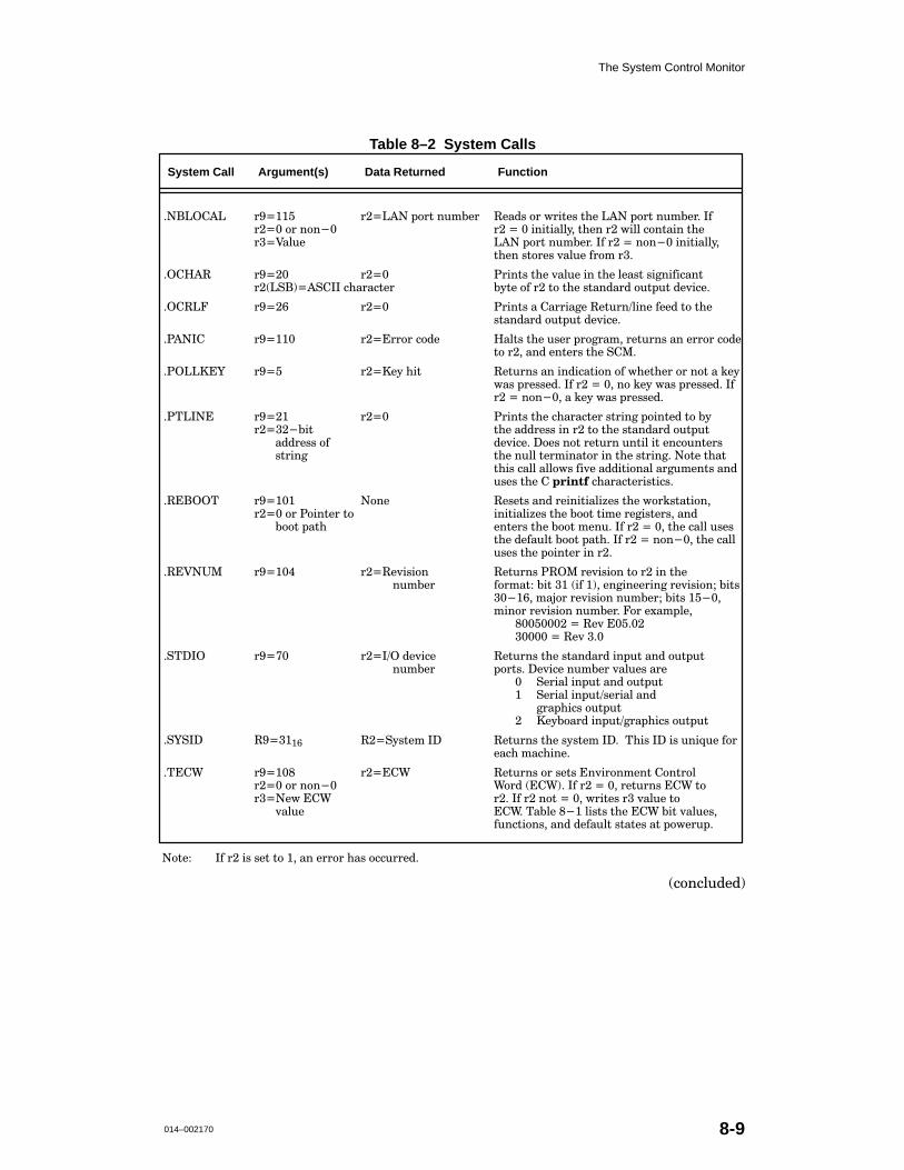
The System Control Monitor
014–002170 8-9
Table 8–2 System Calls
System Call Argument(s) Data Returned Function
� ��!��� ;�� ;��� 98;= 7>6+.; #.*-< 8; @;2=.< =1. �� 98;= 7>6+.;� �/
;�� 8; 787�� ; � � 272=2*55B� =1.7 ; @255 ,87=*27 =1.
;��'*5>. �� 98;= 7>6+.;� �/ ; � 787�� 272=2*55B�
=1.7 <=8;.< ?*5>. /;86 ;��
�!���# ;��� ;�� ";27=< =1. ?*5>. 27 =1. 5.*<= <2072/2,*7=
;��$����$��� ,1*;*,=.; +B=. 8/ ; =8 =1. <=*7-*;- 8>=9>= -.?2,.�
�!�#�� ;��� ;�� ";27=< * �*;;2*0. #.=>;7�527. /..- =8 =1.
<=*7-*;- 8>=9>= -.?2,.�
�"� �� ;��� ;��;;8; ,8-. �*5=< =1. ><.; 9;80;*6� ;.=>;7< *7 .;;8; ,8-.
=8 ;� *7- .7=.;< =1. $���
�"!����) ;�� ;��.B 12= #.=>;7< *7 27-2,*=287 8/ @1.=1.; 8; 78= * 4.B
@*< 9;.<<.-� �/ ; � �� 78 4.B @*< 9;.<<.-� �/
; � 787��� * 4.B @*< 9;.<<.-�
�"%�� � ;�� ;�� ";27=< =1. ,1*;*,=.; <=;270 9827=.- =8 +B
;���+2= =1. *--;.<< 27 ; =8 =1. <=*7-*;- 8>=9>=
*--;.<< 8/ -.?2,.� �8.< 78= ;.=>;7 >7=25 2= .7,8>7=.;<
<=;270 =1. 7>55 =.;627*=8; 27 =1. <=;270� 8=. =1*=
=12< ,*55 *558@< /2?. *--2=287*5 *;0>6.7=< *7-
><.< =1. � ������ ,1*;*,=.;2<=2,<�
�#��!!% ;��� 87. #.<.=< *7- ;.272=2*52C.< =1. @8;4<=*=287�
;�� 8; "827=.; =8 272=2*52C.< =1. +88= =26. ;.02<=.;<� *7-
+88= 9*=1 .7=.;< =1. +88= 6.7>� �/ ; � �� =1. ,*55 ><.<
=1. -./*>5= +88= 9*=1� �/ ; � 787��� =1. ,*55
><.< =1. 9827=.; 27 ;�
�#�' &� ;���� ;�#.?2<287 #.=>;7< "#!� ;.?2<287 =8 ; 27 =1.
7>6+.; /8;6*=� +2= � �2/ �� .7027..;270 ;.?2<287� +2=<
����� 6*38; ;.?2<287 7>6+.;� +2=< ���
6278; ;.?2<287 7>6+.;� �8; .A*695.�
��� ��� � #.? �� ��
����� � #.? ���
�$%��! ;���� ;���! -.?2,. #.=>;7< =1. <=*7-*;- 279>= *7- 8>=9>=
7>6+.; 98;=<� �.?2,. 7>6+.; ?*5>.< *;.
� $.;2*5 279>= *7- 8>=9>=
$.;2*5 279>=�<.;2*5 *7-
0;*912,< 8>=9>=
�.B+8*;- 279>=�0;*912,< 8>=9>=
�$)$�� #���� #�$B<=.6 �� #.=>;7< =1. <B<=.6 ��� %12< �� 2< >72:>. /8;
.*,1 6*,127.�
�%��( ;���� ;���( #.=>;7< 8; <.=< �7?2;876.7= �87=;85
;�� 8; 787�� (8;- ���(�� �/ ; � �� ;.=>;7< ��( =8
;�� .@ ��( ;� �/ ; 78= � �� @;2=.< ;� ?*5>. =8
?*5>. ��(� %*+5.��� 52<=< =1. ��( +2= ?*5>.<�
/>7,=287<� *7- -./*>5= <=*=.< *= 98@.;>9�
8=.� �/ ; 2< <.= =8 � *7 .;;8; 1*< 8,,>;;.-�
�,87,5>-.-�

The System Control Monitor
014–0021708-10
SCM SubroutinesIn addition to system calls, the System Control Monitor (SCM) supports hardwiredentry points to subroutines in Table 8–3 (accessible with a jsr instruction containingthe appropriate entry point).
Table 8–3 SCM Subroutines
���� ������ �� ����� ������ ������� �� ����� � �� ���
���� � ���� ���� ����� ������ ����� ����� � �� ���
Entry Point(Hex) Subroutine Argument Description
SCM CommandsThe System Control Monitor (SCM) has commands to control and debug programs,boot media, and change system configuration parameters.
A command line consists of one valid SCM command and possibly one or morearguments.
If a command is issued incorrectly, the SCM displays a general message (ex. Invalidcommand, Requires argument(s), Invalid argument(s)) and then returns the prompt.
Type a maximum of 80 characters per command line. You do not have to type theentire command name; the SCM accepts the first letter of a command.
SCM commands and arguments are not case–sensitive, with the exception of devicespecification arguments to the BOOT command, which must be lowercase.
The SCM supports several keyboard control characters. Table 8–4 describes controlsequences used to edit command lines, interrupt and exit from SCM commands, andrestore configuration parameters.
Address and Data ConventionsThe address arguments used in SCM commands consist of two 16–bit, hexadecimalwords. You may omit leading zeros. SCM commands support physical and logicaladdress arguments according to the current mode of the memory management unit(MMU). When address translation is on, logical addresses map to physical addresses.
The assembler assumes data is decimal unless there is a dollar sign ($) preceding thedata to indicate hexadecimal. The disassembler returns hexadecimal data. TheSCM displays data output mnemonics and accepts data input mnemonics by default,since both the assembler and disassembler are enabled by default.
With address translation on, the SCM displays the contents of a memory locationusing the following format:

The System Control Monitor
014–002170 8-11
Memory logicaladdress – physicaladdress / data – mnemonic
For example, if the contents of memory location 10 is 5555FFFF16 the SCM displaysthe following:
Memory 00000010 – 00000010 / 5555FFFF – xor.u r10 r21 $FFFF
The data mnemonic includes the opcode (xor.u in the example above), the registerspointed to by the first 16–bit word of the 32–bit address (r10 and r21), and thehexadecimal data in the second word of the address (FFFF).
Table 8–4 SCM Line Editing and Keyboard Control Commands
� �*(+'!/!. /$! �0--!)/ %)+0/ '%)!� �!#%). !3!�0/%*) *"
�*((�) %)+0/� �) -!/0-). /$! ��� +-*(+/�
�Ctrl–A �!��''. �) %.+'�4. /$! '�./ �*((�) ./-%)# 4*0 !)/!-!
�/ /$! ��� +-*(+/�
�Ctrl–C � �)/!--0+/. !3!�0/%*) *" �) ��� �*((�) �) -!/0-). /$!
��� +-*(+/� �$%. %. � +*''! %)/!--0+/� .*(! +-*�! 0-!.
�*(+'!/! �!"*-! /$!4 �-!�&� �" 4*0 * )*/ $�1! �)
�0/*�-!+!�/ &!4�*�- � !3!�0/! /$! �/-'�� .!,0!)�!
-!+!�/! '4 0)/%' 4*0 .!! /$! ��� +-*(+/�
�Ctrl–I Restores default configuration parameters to the followingfactory settings. System console port: 9600 baud, 8 databits, no parity, ANSI character set, enabled flow control,U.S. English keyboard language. Parallel printer:Centronics interface. SCSI tape drives: block transfermode. Mouse or modem port: 1200 baud. Also restoresvideo timing parameters. Enter <Ctrl–I>, wait until youhear one beep; then, enter 1 if you have a 70 Hz. monitor,or enter 2 for a 60 Hz. monitor.
�Ctrl–P �%.+'�4. /$! �0--!)/ ./�/! *" /$! �)1%-*)(!)/ �*)/-*'
�*- ������
�Ctrl–Q �!.0(!. ��� *0/+0/ %.+'�4 /$�/ 2�. .0.+!) ! 2%/$ /$!
�/-'�� .!,0!)�!�
�Ctrl–S �0.+!) . ��� *0/+0/ %.+'�4 0)/%' 4*0 -!.0(! %/ 2%/$ /$!
�/-'�� .!,0!)�!�
�Ctrl–U �-�.!. /$! �0--!)/ '%)! *" /!3/� "-*( /$! '!"/ *" /$! �0-.*-
/* /$! ��� +-*(+/�
�!4�*�- �)/-4 �0)�/%*)
� �$! �!2 �%)! �) �)/!- &!4. $�1! .+!�%�' "0)�/%*). 2$!) 0.! 2%/$ /$! EXAMINE �*((�) ��
� �)'4 "0)�/%*). �. �) %)/!--0+/ /* ��� "0)�/%*).�
�3!�0/! /$%. .!,0!)�! *)'4 2$%'! %) /$! ����
�)'4 2*-&. 2$!) �'*2 �*)/-*' +-*/*�*' %. !)��'! 2%/$%) /$! ����

The System Control Monitor
014–0021708-12
Table 8–5 SCM Commands
� �#�$�"�� �%#��+% #$"��%%"$ %&�&'% ��'���!�
Attach �#������% �&&����� #$"��%%"$ �$"�$� �"!&$"��
%+%&� "#�$�&�"!
Boot �&�$&% %+%&� �$" �""&%&$�# ��(��� ��� �!%&����&�"! �""��
Continue ��%&�$&% �&&����� #$"��%%"$ �$"�$� �"!&$"�� ���'���!�
Display ��")% $���%&�$ ���� �"!&�!&% ��'���!�
Examine �#�! "$ ���& �"!&�!&% "� ��'���!�
$���%&�$% �!� � "$+ �"��&�"!%
Format �%#��+% ���) "$ ���!�� ��� �!%&����&�"! �""��
�"!���'$�&�"! �!'
Help �%&% (���� ��� �" �!�% �+%&� "#�$�&�"!� ���'���!�
#$"�$� �"!&$"�
Initialize �$�&�% ��&� &" � $�!�� "� � "$+ ��'���!�
Locate ���$���% � "$+ �"$ � ��&� #�&&�$! ��'���!�
Move '#����&�% � � "$+ ��"�� �! !�) ��'���!�
�"��&�"!
Onestep *��'&�% &�� !�*& #$"�$� �!%&$'�&�"! ��'���!�� #$"�$� �"!&$"�
Prompt ���!��% &�*& "� ��� #$" #& ��� �!%&����&�"! �""��
Reset �!�&����,�% %+%&� &" #")�$�'# %&�&� �+%&� "#�$�&�"!
Start ����!% #$"��%%"$ �& %#������� �$"�$� �"!&$"��
���$�%% %+%&� "#�$�&�"!
Trap ���)% "$ �!%�$&% �$���#"�!&% ��'���!�
Untrap �� "(�% �$���#"�!&% ��'���!�
View �%#��+% � $�!�� "� � "$+ ��'���!�
Write �!%�$&% ��&� �! "!� � "$+ �"��&�"! ��'���!�
Zloader �&�$&% %�$��"$� �"���$ '&���&+ ��� �!%&����&�"! �""��
�" �!� �%�$�#&�"! �'!�&�"!

The System Control Monitor
014–002170 8-13
�� ����� � �������� � ������ �� �������
COMMAND–NAMECommand description.
COMMAND argument [argument]
NOTE: The minimal mnemonic for each command is always the first letter of thecommand name.
Description
Describes the command.
Arguments
Defines the arguments.
None The command accepts no arguments.
argument The command requires the argument defined here.
[argument] The argument is optional; do not include brackets.
Related Commands
Lists closely related SCM commands.
Related Messages
Lists messages that may appear after invoking the command.
Examples
Examples of the command.

The System Control Monitor
014–0021708-14
. (period)Display job processor status.
. (period)
Description
The . (period) command displays the status of the attached job processor and itsprogram registers.
The status includes the following:
• PSR (Processor Status Register)The processor state of the program that was last running on the attachedprocessor. The PSR is the value in Control Register 1 (cr1).
• XPC (Execute Program Counter)The contents of the program counter (PC) of the program that caused entry intothe SCM. XPC is from Control Register 4 (cr4).
• DCSH (Data Cache Enable/Disable)The state of the user program data cache before entering the SCM. Y indicatesenabled, and N indicates disabled.
• DMMU (Data Memory Management Unit Enable/Disable)The state of the user program data MMU before entering the SCM. Y indicatesenabled, and N indicates disabled.
• ICSH (Instruction Cache Enable/Disable)The state of the user program instruction cache before entering the SCM. Yindicates enabled, and N indicates disabled.
• IMMU (Instruction Memory Management Unit Enable/Disable)The state of the user program instruction MMU before entering the SCM. Yindicates enabled, and N indicates disabled.
Arguments
None
Related Commands
Attach Specify the attached processor in multiprocessor systems.
Continue Resume program execution at the program counter value of thecurrently attached processor.
Onestep Execute the next single instruction of a program and then displaytrace information.

The System Control Monitor
014–002170 8-15
Related Messages
None
Examples
• Display processor status on single processor system.
SCM> .
PSR XPC DCSH DMMU ICSH IMMU
A00003F2 FFC039DE N N N N
• Display processor status information on multiprocessor system.
Jp#0/SCM> .
Jp#0/PSR XPC DCSH DMMU ICSH IMMU
A00003F2 FFC039DE N N N N

The System Control Monitor
014–0021708-16
ATTACHSpecify active job processor.
ATTACH �����
Description
Attach is only valid for multiprocessor systems. It allows you to attach the SCM toa specified job processor for subsequent operations (in other words, it makes aparticlar processor active). Unattached processors remain in an idle state. The SCMprompt indicates which job processor is currently attached (Jp#n/SCM> where n isthe number of the attached job processor). By default, Jp#0 is the attached processorafter powerup.
Attach returns the currently attached processor if used without an argument.
Arguments
[jp#] The number of the job processor to attach.
Related Commands
. (period) Display the status of the attached processor.
Continue Resume program execution at the program counter value of thecurrently attached processor.
Prompt Change the SCM prompt text.
Start Execute a program from a specified address.
Related Messages
Jp#n attached
Examples
• Attach SCM to job processor #1.
Jp#0/SCM> A 1
Jp#1 attached
• Display the currently attached job processor.
Jp#1/SCM> A
Jp#1 attached

The System Control Monitor
014–002170 8-17
BOOTStarts the system from a specified device.
BOOT [device][file]
NOTE: For more information on the Boot command, see “Starting AViiON 6280Series Systems” (DG # 014–002178).
Description
BOOT resets the system hardware; then it loads a bootstrap program from a devicespecified in the dev argument. The argument format conforms to the common objectfile format (coff) defined in section 4 of the Binary Compatibility Standard (BCS).
When you use BOOT without an argument, the SCM boots from a default boot path.If the default boot path is not initialized or not valid, the SCM tries to find a validbootstrap file according to a hardcoded probe sequence.
Arguments
device([controller([ctrlr_num,ctrlr_id])],[unit],[lun])The device specification (first–stage boot) consists of a mnemonicthat identifies the type of device and names the device driver, plusoptional parameters that provide additional information to fullyspecify that device.
[ld:][/dir...]file Specifies an executable filename or an Internet host address, usedand defined by the bootstrap program in a second–stage bootsequence.
Related Commands
FORMAT Displays the View or Change System Configuration menu. You candisplay the Change Boot Parameters menu from this menu.
Related Messages
Booting from ...
Unable to load boot file ...
Examples
1. Boot the default system boot path.
Jp#0/SCM> b

The System Control Monitor
014–0021708-18
2. Boot from file #0 on the first tape drive (SCSI ID#4).
Jp#0/SCM> b st(dgsc(),4)
(Default third parameter and second stage boot: specifiesst(dgsc(),4,0)0 )
3. Boot from the third file on the tape in the second tape drive (SCSI ID#5).
Jp#0/SCM> b st(dgsc(),5)2
4. Boot your DG/UX operating system kernel to run level 3.
Jp#0/SCM> b sd(dgsc()root:/dgux –3
5. Boot AViiON System Diagnostics (the program file diags located in the directorycalled stand on the logical disk usr) from the default system disk.
Jp#0/SCM> b sd(dgsc(),0)usr:/stand/diags
6. Boot any executable file called bootfile in the root directory on the second SCSIdisk (SCSI ID#1).
Jp#0/SCM> b sd(dgsc(),1)root:/bootfile
7. Boot from the host at Internet address 128.111.5.6 on a VLC Ethernet LAN.
Jp#0/SCM> b hken()128.111.5.6:

The System Control Monitor
014–002170 8-19
CONTINUERestart attached processor.
CONTINUE [trace–count]
Description
Continue resumes program execution at the address stored in the program counter(NPC) of the attached processor, for the number of instructions specified in theoptional trace count argument. The NPC is CR5 (Control Register 5). When you usethe command without the trace count argument, system control passes completely tothe continued program.
Arguments
[trace–count] The number of instructions to execute (in hexadecimal). The systemdisplays the address, data, and mnemonic (in that order) after eachinstruction, then halts, displays the processor status, and returnsthe SCM prompt.
Related Commands
. (period) Display the status of the attached processor, including the value ofthe NPC.
Attach Specify the attached processor in multiprocessor systems.
Display Show the contents of all register files.
Start Execute a program from a specified address.
Related Messages
None
Examples
• Resume program execution at the NPC value; leave the SCM.
SCM> C
• Resume program execution at the current PC value, display trace informationafter the next three instructions; then halt the processor and return to the SCM.

The System Control Monitor
014–0021708-20
SCM> C 3
Trace 00000010 5555FFFF xor.u r10 r21 $ffffTrace 00000014 00000000 xmen.bu r0 r0 $0Trace 00000018 00000000 xmen.bu r0 r0 $0
PSR XPC NPC FPC DCSH DMMU ICSH IMMU
A0000000 0000001A 0000001E 00000022 Y Y N N
SCM>

The System Control Monitor
014–002170 8-21
DISPLAYShow contents of register files.
DISPLAY
Description
Display shows the contents of general register files (r), control register files (cr), andfloating–point control registers (fcr) in the attached processor. Without anargument, only general register files are displayed.
Arguments
None
Related Commands
Attach Specify the attached processor in multiprocessor systems.
Examine Display and/or change specified registers or memory.
Related Messages
None
Examples
Display the current content of all register files.
SCM> D
r00 = 00000000 r01 = 00066B58 r02 = FFC00000 r03 = 00000000 r04 = 0000000C r05 = FFF00000 r06 = 0016E570 r07 = 0016B340 r08 = 00003230 r09 = 00000063 r10 = 00000998 r11 = FFFFFFA1 r12 = 00000000 r13 = 00000000 r14 = 00000000 r15 = 00000000 r16 = 00000000 r17 = 00000000 r18 = 00000000 r19 = 00000000 r20 = 00000000 r21 = 00000000 r22 = 00000000 r23 = 00000000 r24 = 0016E570 r25 = 0000002C r26 = 000E0000 r27 = 000F0000 r28 = 00010000 r29 = 00000000 r30 = 017DEFD0 r31 = 017DEFC8 cr00 = FFF8113C cr01 = 800003FB cr02 = 800003f0 cr03 = 00000000 cr04 = 0006009A cr05 = 0006009E cr06 = 000600A2 cr07 = FFC00000 cr08 = 0000403F cr09 = 0000403F cr10 = 017DEF40 cr11 = 00000000 cr12 = 017DEF58 cr13 = 017DEF4C cr14 = 00000000 cr15 = 00000000 cr16 = 00000000 cr17 = 00066B58 cr18 = FFC00000 cr19 = 00000000 cr20 = 00000000fcr00 = 00000000fcr01 = 00000000 fcr02 = 00000000fcr03 = 00000000fcr04 = 00000000fcr05 = 000048A2 fcr06 = 00000000fcr07 = 00000000fcr08 = F8004808fcr62 = 00000001 fcr63 = 00000000

The System Control Monitor
014–0021708-22
EXAMINEOpen and optionally change the contents of selected register ormemory locations.
[M] addressH addressQ address RnumberCRnumber FCRnumber
EXAMINE
Description
Examine opens and displays the contents of a specified memory address or registerfile. After opening a memory location, you can use special key functions described inTable 8–6 to enter new data, open the next or previous memory location, or return tothe SCM prompt without making changes.
CAUTION: There are no restrictions to the areas of memory you can modify;modifying system control registers or NOVRAM locations could halt thesystem or destroy necessary system information. Ctrl–C will not recoverdata already modifed.
Use one argument per command line to specify whether you want to open a memorylocation or register file, and whether to view memory locations in word (32 bit),half–word (16 bit), or quarter–word (8–bit, or single byte) increments.
Without an argument, the Examine command opens and displays the last memoryaddressed examined. After the system halts or the first time after powerup, the SCMopens memory location 0 when you use the command without an argument.
Table 8–6 Special Key Functions for EXAMINE Command
��, � $�
%' �'��! ��
�*$�) %$ � )� ������� %##�$�
�'' ���
��)*'$
�(��&�
�� �)��
�' )�( ��)� � �$)�'��� )��$ �"%(�( )�� #�#%'.
"%��) %$ %' '�� ()�' �$� '�)*'$( )�� �� &'%#&)�
���$ � '�� ()�' � "� ( %&�$� �"%(�( )�� '�� ()�'
�$� '�)*'$( )�� �� &'%#&)� ���$ �
#�#%'. "%��) %$ ( %&�$� ,' )�( ��)� � �$/
)�'��� �"%(�( )�� �*''�$) #�#%'. "%��) %$� �$�
%&�$( )�� $�-) "%��) %$�
�)�$��'� �
��.�%�'�
�� ��
��.�%�'�
�$)�'
�� �)�� ���$ � '�� ()�' � "� ( %&�$� �"%(�( )�� '�� ()�'
�$� '�)*'$( )�� �� &'%#&)� ���$ � #�#%'.
"%��) %$ ( %&�$� ,' )�( ��)� � �$)�'��� �"%(�( )��
�*''�$) #�#%'. "%��) %$� �$� %&�$( )�� &'�+ %*(
"%��) %$�

The System Control Monitor
014–002170 8-23
Argument
[[M] address] The 32–bit (single word) memory location you want to examine ormodify. Typing M is optional. If you type a number without a M, H,Q, R, CR, or FCR before it, the SCM interprets the number as a32–bit memory address. Any address is masked to be a true 32–bitword (bits 0 and 1 are cleared).
[H address] The 16 bits (half–word) of memory you want to examine or modify.You must type H, followed by a space and the memory location. Anyaddress is masked to be a true half–word (bit 0 is cleared).
[Q address] The 8 bits (one byte) of memory you want to examine or modify. Youmust type Q, followed by a space and the memory location. Noaddress masking.
[Rnumber] The CPU register file you want to examine or modify. You must typeR. Valid entries are R0 through R31.
[CRnumber] The control register you want to examine or modify. You must typeCR. Valid entries are CR0 through CR20.
[FCRnumber] The floating point register you want to examine or modify. You musttype FCR. Valid entries are FCR0 through FCR8, FCR62, orFCR63.
Related Commands
Display Show the contents of all register files.
Related Messages
None
Examples
NOTE: The examples in this section include keyboard characters for a standard IBM PC AT–compatible keyboard.
• Display the contents of memory address 1000 without modifying. Disassemblerand MMU are disabled in this example.
SCM> E M 1000 or SCM> E 1000
Memory 00001000 / 58670004 < Esc>
SCM>
• Display the contents of memory address 1000 without modifying. Disassemblerand MMU are enabled in this example.

The System Control Monitor
014–0021708-24
SCM> E 1000
Memory 00001000 – 00001000/12345678 – ld.d r17 r20 $5678Esc
SCM>
• Display without modifying the contents of last memory address examined.
SCM> E
Memory 00001000 – 00001000/12345678 – ld.d r17 r20 $5678Esc
SCM>
• Display without modifying the contents of register file r03.
SCM> E R3 or SCM> E R03
R03 = 00000000
SCM>
• Display without modifying the contents of control register file cr01.
SCM> E CR01 or SCM> E CR1
r03 = 80000F3B
SCM>
• Enter data 12345678 in memory address 1000; then exit from the command andreturn to the SCM.
SCM> E M1000 or SCM>E 1000
Memory 00001000 / 58670004 12345678 <Esc>
SCM>
• Display the contents of memory address 1000; deposit data 12345678 in memoryaddress 1004; then return to the SCM.
Jp#0/SCM> E 1000
Memory 00001000 / 12345678 < CR>
Memory 00001004 / 58670004 12345678 <Esc>
SCM>
• Display the contents of floating–point control register file fcr62; then deposit data5555FFFF into fcr62.
SCM> E FCR62
fcr62 = 00000000 5555FFFF
SCM>
• Display the first 16 bits at location 1000.

The System Control Monitor
014–002170 8-25
SCM> E H 1000
Memory 00001000 / 1234 < Esc>
SCM>
• Display the first 8 bits at location 1000.
SCM> E Q 1000
Memory 00001000 / 12 < Esc>
SCM>
The System Control Monitor
014–0021708-26
FORMATDisplays Configuration Menus.
FORMAT
Description
Format displays the “View or Change System Configuration” menu.
To return to the SCM prompt, press New Line or select the last item in the “View orChange System Configuration” menu.
Arguments
None
Related Commands
Boot Boot a device or display the Change Boot Parameters menu.
Related Messages
None
Examples
None
The System Control Monitor
014–002170 8-27
HELPDisplay available SCM commands.
HELP
Description
Displays an alphabetical list of the minimal mnemonic for valid SCM commands, thearguments each command accepts, and a brief command description.
Arguments
None
Related Messages
None
Examples
None

The System Control Monitor
014–0021708-28
INITIALIZEWrite specified data to a range of memory.
INITIALIZE data beg–addr end–addr
Description
The Initialize command writes specified data to a range of memory addresses thatstarts at the specified 32–bit beginning address and ends at the 32–bit endingaddress.
CAUTION: There are no restrictions to areas of memory you can initialize.Initializing system control registers or NOVRAM locations could halt thesystem or destroy necessary data. Use the Ctrl–C sequence to exit fromthe command during processing.
Arguments
data Content written to each location of the memory range you areinitializing.
beg–addr First location in the range of memory.
end–addr Last location in the range of memory.
Related Commands
Move Duplicate the contents of a specified source range and write it to aspecified destination range.
View Display the contents of a range of memory.
Write Write data to a single memory location.
Examples
Initialize memory by writing 5555FFFF to a range of memory beginning at address 0and ending at 10. Then view the memory range to see the results.
Jp#1/SCM> I 5555FFFF 0 10
Jp#1/SCM> VIEW 0 10
Memory 00000000 / 5555FFFF – xor.u r10 r21 $FFFFMemory 00000004 / 5555FFFF – xor.u r10 r21 $FFFFMemory 00000008 / 5555FFFF – xor.u r10 r21 $FFFFMemory 0000000C / 5555FFFF – xor.u r10 r21 $FFFFMemory 00000010 / 5555FFFF – xor.u r10 r21 $FFFF

The System Control Monitor
014–002170 8-29
LOCATEFind a specified data pattern in memory.
LOCATE data [beg–addr] [end–addr]
Description
Locate searches memory for a specified data pattern; then displays the address andcontents of each location in which it finds the data. You can omit the addressarguments and search all of physical memory, specify a starting address only, orspecify a range of memory with starting and ending address arguments.
NOTE: A search through all of memory could take several hours! To stop a searchbefore it completes, use Ctrl–C.
Arguments
data Pattern in memory for which the system searches.
[beg–addr] Location in memory where system begins searching. If you specifyonly one address argument, the system interprets it as a startingaddress.
[end–addr] Location in memory where system stops searching.
Related Commands
Move Duplicate the contents of a specified source range and write it to aspecified destination range.
View Display the contents of a range of memory.
Related Messages
None
Examples
• Locate each occurrence of data pattern 01234567 in a range of memory beginningat 0 and ending at 1000; then display the address of each occurrence.
Jp#1/SCM> L 01234567 0 1000
Memory 00000800 / 01234567 – ld.d r17 r20 $4567

The System Control Monitor
014–0021708-30
• Locate each occurrence of data pattern 01234567 in all of main memory.
Jp#1/SCM> L 01234567
Memory 00000800 / 01234567 – ld.d r17 r20 $4567Memory 00001200 / 01234567 – ld.d r17 r20 $4567

The System Control Monitor
014–002170 8-31
MOVEDuplicate a block of memory.
MOVE count source–addr dest–addr
Description
The Move command copies the block of data that begins at the source address andends after the specified count of 32–bit words; then moves the copy into a block of thesame size starting at the destination address.
CAUTION: There are no restrictions to areas of memory into which you can movedata. Overwriting data in system control registers or NOVRAMlocations could halt the system or destroy necessary data. Use the Ctrl–Csequence to exit from the command during processing.
Arguments
count Hexadecimal number of 32–bit words from the beginning address tothe end of the block to be moved. There is no maximum orminimum block size.
source–addr Memory location at the beginning of the range to be moved.
dest–addr Memory location at the beginning of the range the block is movingto.
Related Commands
Initialize Write data to a range of memory.
Locate Search memory for a data pattern.
View Display the contents of a range of memory.
Related Messages
None
Examples
• Move the data block beginning at memory address 0 and spanning 4F words todestination address 8000.
Jp#1/SCM> M 4F 0 8000

The System Control Monitor
014–0021708-32
• Move the block that begins at 0 and spans 5 words to destination address 400.First, view the range of memory from locations 0 through 10.
Jp#1/SCM> VIEW 0 10
Memory 00000000 / 5555FFFF – xor.u r10 r21 $FFFF Memory 00000004 / 5555FFFF – xor.u r10 r21 $FFFF Memory 00000008 / 5555FFFF – xor.u r10 r21 $FFFF Memory 0000000C / 5555FFFF – xor.u r10 r21 $FFFF Memory 00000010 / 5555FFFF – xor.u r10 r21 $FFFF
Next, move the block.
Jp#1/SCM> M 5 0 400
Finally, view the contents of the block of memory from locations 400 through 410.
Jp#1/SCM> V 400 410
Memory 00000400 / 5555FFFF – xor.u r10 r21 $FFFF Memory 00000404 / 5555FFFF – xor.u r10 r21 $FFFF Memory 00000408 / 5555FFFF – xor.u r10 r21 $FFFF Memory 0000040C / 5555FFFF – xor.u r10 r21 $FFFF Memory 00000410 / 5555FFFF – xor.u r10 r21 $FFFF

The System Control Monitor
014–002170 8-33
ONESTEPExecute next step of a program.
ONESTEP [trace–count]
Description
The Onestep command begins program execution at the address stored in theprogram counter (CR5) in increments of one instruction. It displays traceinformation after each instruction executes. With no argument, the system executesthe single program instruction stored in CR5; then halts and displays statusinformation.
Arguments
[trace–count] Hexadecimal number of instructions to be executed one by one (insingle steps) before the processor halts.
Related Commands
. (period) Display the status of the attached processor.
Continue Resume program execution at the program counter value of thecurrently attached processor.
Start Execute a program from a specified address.
Related Messages
None
Examples
• Execute the instruction pointed to by the program counter.
SCM> 0
PSR XPC DCSH DMMU ICSH IMMU
A0000000 FF001602 Y N N N

The System Control Monitor
014–0021708-34
• Execute three instructions one by one, beginning with the instruction pointed toby the PC.
SCM> 0 3
Trace 00000010 5555FFFF xor.u r10 r21 $FFFFTrace 00000014 00000000 xmen.bu r0 r0 $0Trace 00000018 00000000 xmen.bu r0 r0 $0
PSR XPC DCSH DMMU ICSH IMMU
A0000000 0000001A N N N N

The System Control Monitor
014–002170 8-35
PROMPTChanges SCM prompt text prefix.
PROMPT [new–prompt]
Description
Prompt changes the default SCM prompt to a specified ASCII string. This can beuseful to uniquely identify multiple systems. The right bracket symbol (>) appearsafter the text prefix; if you change the prompt text to a null text string, your promptis the right bracket symbol.
NOTE: Multiprocessor systems add the text string Jp#n/ (n = the number of theattached job processor) to the default prompt text.
Arguments
[new–prompt] Text string of ASCII characters to replace the prompt. The ASCIIstring can have as many as 1510 characters. There are no characteror symbol restrictions.
Related Commands
Attach Specify the attached job processor in a multiprocessor system.
Related Messages
Argument(s) out of range
Examples
1. Display the current SCM prompt; then change it to AV5000.
Jp#0/SCM> P
Jp#0/SCM>
Jp#0/SCM> P AV5000
Jp#0/AV5000>

The System Control Monitor
014–0021708-36
RESETRestore system to power–up state.
RESET
Description
Initializes system elements (excluding memory) to their original power–up state.Unlike a cold reset (power applied to the system), a warm reset (initiated by software,the Reset command, or a Reset switch) does not initialize memory or run power–updiagnostics.
CAUTION: Be careful not to enter R at the SCM prompt accidentally. You cannotuse Ctrl–C or an SCM command to recover.
NOTE: In systems with Motorola 88204 CMMUs, RESET does not reset the serialinterface; reset this serial interface via the DUART Reset (DRE bit 28) bit ofthe Control (CON) register as described in 5, “Memory”.
Arguments
None
Related Commands
Boot Boot a device.
Related Messages
System Reset
Examples
• Reset the system (processors, keyboard interface, graphics interface, etc.).
SCM> R
PSR XPC DCSH DMMU ICSH IMMU
A00003F2 FFC039DE N N N N

The System Control Monitor
014–002170 8-37
STARTStart job processor at specified address.
START address [trace–count]
Description
The Start command begins executing a program at the main memory addressspecified. The operating system or user program resumes system control unless youuse the trace–count argument.
Arguments
address Memory location at which the processor starts executing.
[trace–count] The system displays the address, data, and mnemonic (in thatorder) after executing the hexadecimal number of instructions youspecify with this argument. Then the system halts and the monitordisplays status information.
Related Commands
Boot Boot a device.
Continue Resume program execution at the program counter value of thecurrently attached processor.
Onestep Execute the next single instruction of a program and then displaytrace information.
Related Messages
None
Examples
• Start processor executing at address 398F0.
SCM> S 398F0
• Start processor executing at address 398F0 with a trace count of 3.
SCM> S 398F0 3
Trace 000398F0 5555FFFF xor.u r10 r21 $FFFFTrace 000398F4 00000000 xmen.bu r0 r0 $0Trace 000398F8 00000000 xmen.bu r0 r0 $0
PSR XPC DCSH DMMU ICSH IMMU
A0000000 000398FA Y Y N N

The System Control Monitor
014–0021708-38
TRAPView or insert breakpoints.
TRAP [address] ...
Description
Insert a breakpoint at the specified address. You can insert up to 2010 breakpoints.The command does not allow duplicate breakpoints.
With no argument, Trap displays a list of all current breakpoints.
NOTE: The SCM implements breakpoints with the trap exception; hence, thecommand names Trap and Untrap.
Arguments
[address] Memory location at which you want to insert a breakpoint.
... The memory location of each subsequent breakpoint (when youinsert more than one breakpoint per command line).
Related Commands
Untrap Delete breakpoint(s)
Related Messages
None
Examples
• Insert a breakpoint at addresses 5000 and 77000.
SCM> T 5000 77000
Breakpoint # 1 – 00005000 SetBreakpoint # 2 – 00077000 Set
• Display the current list of breakpoints and their addresses.
SCM> T
Breakpoint # 1 – 00005000Breakpoint # 2 – 00077000
No response indicates there are no current breakpoints.

The System Control Monitor
014–002170 8-39
UNTRAPDelete breakpoints.
UNTRAP [breakpoint] ...
Description
The Untrap command removes the breakpoint number(s) specified, or removes allcurrent breakpoints with no argument. To view current breakpoint numbers, use theTrap command.
Arguments
breakpoint Number of the breakpoint you want to remove. (A decimal number1 through 20.)
... Numbers of each additional breakpoint number you want to remove.
Related Commands
Trap Insert a breakpoint at specified address, or display the currentbreakpoints.
Related Messages
Invalid breakpoint
Examples
• Find the three current breakpoints; then remove two of them.
SCM> T
Breakpoint # 1 – 00005000Breakpoint # 2 – 00077000Breakpoint # 3 – 000C6001
SCM> U 1 3
Breakpoint # 1 deleted Breakpoint # 3 deleted
• Remove all current breakpoints.
SCM> U

The System Control Monitor
014–0021708-40
VIEWDisplay a range of memory.
VIEW beg–addr [end–addr]
Description
The View command displays the contents of a specified block of contiguous memory.If you use the command with only a beginning address, the SCM displays all ofmemory from the specified address to the top of memory address.
NOTE: There are no restrictions to areas of memory you can specify. Viewing largeblocks of memory could take hours, or cause memory exceptions. Use theCtrl–C sequence to exit before completing the operation.
From left to right, the system displays the logical memory address, the physicalmemory address (only when MMU is enabled), the contents of the address, and theinstruction mnemonic.
Arguments
beg–addr First memory address in the range you want to view.
[end–addr] Last memory address in the range you want to view.
Related commands
Initialize Write data to a range of memory.
Locate Search memory for a data pattern.
Move Duplicate the contents of a specified source range and write it to aspecified destination range.
Write Write data to a single memory location.
Examples
• View the contents of a block of contiguous memory beginning at location 0 andending at location 00000010.
SCM> V 0 10
Memory 00000000 / 5555FFFF – xor.u r10 r21 $FFFFMemory 00000004 / 5555FFFF – xor.u r10 r21 $FFFFMemory 00000008 / 5555fFFF – xor.u r10 r21 $FFFFMemory 0000000C / 5555FFFF – Xor.u r10 r21 $FFFFMemory 00000010 / 5555FFFF – xor.u r10 r21 $FFFF

The System Control Monitor
014–002170 8-41
WRITEInsert data in one memory location.
WRITE [H] [Q] address data
Description
Write writes data to a specified address.
CAUTION: Write executes immediately; you cannot exit using Ctrl–C. There are nowrite restrictions; although writing data to system control registers orNOVRAM could halt the system or destroy necessary data.
Arguments
[H] Address and data are 16–bits.
[Q] Address and data are 8–bits.
address Address to write data.
data Hexadecimal data or assembler command.
Related Commands
Examine Display and/or change specified registers or memory.
Related Messages
None
Examples
• Write 32 bits (one word) of data (01234567) to address 800.
SCM> W 800 01234567
• Write 16 bits (one half–word) of data (1234) to address 800.
SCM> W H 800 1234
• Write 8 bits (one byte) of data (12) to address 800.
SCM> W Q 800 12 or SCM> W B 800 12
The System Control Monitor
014–0021708-42
ZLOADERStart the s–record load utility.
ZLOADER
Description
Zloader executes a program that downloads files in Motorola s–record format (S3/S7type) to memory from a device connected to the system console port. The SCMrecognizes s–records only after you use the Zloader command.
An s–record is a file that contains an unlimited number of records; each record has amaximum of 256 bytes. Servers use s–records to download files serially. The loaderutility copies s–records from the serial port to system memory. The SCM readsinformation appended to individual s–records, stores each record at locationsspecified in the s–record header, and then verifies checksums. Information appendedto the last s–record notifies the SCM when the entire file has been sent.
For this command to function, you must configure the system to use an s–recordutility and a server must send s–record files. If you are not familiar with thes–record loader utility, if the system is not configured to receive s–records, or if theserver is not sending, press the Ctrl–C sequence to exit from the Zloader command.
NOTE: The system will pause until it receives the last s–record in a file, or untilyou execute a Ctrl–C command sequence to exit to the SCM prompt.
Arguments
None
Related Commands
None
Related Messages
DLL Started DLL (downline loader) is an s–record load utility
DLL Done
Examples
None
�� � ���� ��

A–1014–002170
Appendix AAddress Map
#0- .5225;14/ 9)*2- 18 ) 3)6 5. ),,7-88)*2- 25+)91548 ;19014 �%11�� ���� 8-71-8 8=89-38�
Table A–1 Address Map
$8-7 "6)+- ����� �*=9-8� ���� ���� � ���� ����� � � � � � � � � � � � � � � � � � � � � � � � � � � � �
"=89-3 �-357= ��!��� �� �� 3)<13:3 ���� ���� � ���� ����� � � � � � � � � �
��#�� �22 8=89-3 3-357= 3:89 *- +5491/:5:8��
�� 86)+- ���� ���� � ���� ����� � � � � � � � � � � � � � � � � � � � � � � � � � � � � � � � � � � � � � � � �
�� 86)+- ��� �*=9-8� ���� ���� � ���� ����� � � � � � � � � � � � � � � � � � � � � � � � � � � � � �
�� 86)+- ��� �*=9-8� ���� ���� � ���� ����� � � � � � � � � � � � � � � � � � � � � � � � � � � � � �
$91219= "6)+- � �*=9-8� ���� ���� � ���� ����� � � � � � � � � � � � � � � � � � � � � � � � � � � � � � �
� !�� ���� �*=9-8� ���� ���� � ��� ����� � � � � � � � � � � � � � � � � � � � � � � � � � � � � � �
� ��� ���� ����� � � � � � � � � � � � � � � � � � � � � � � � � � � � � � � � � � � � � � � � � � � �
� �"# ���� ����� � � � � � � � � � � � � � � � � � � � � � � � � � � � � � � � � � � � � � � � � � � � �
'��! ���� ����� � � � � � � � � � � � � � � � � � � � � � � � � � � � � � � � � � � � � � � � � � � � �
��#��! ���� ���� � � � � � � � � � � � � � � � � � � � � � � � � � � � � � � � � � � � � � � � � �
�#(��#� ���� ���� � � � � � � � � � � � � � � � � � � � � � � � � � � � � � � � � � � � � � � �
�#("� ���� ����� � � � � � � � � � � � � � � � � � � � � � � � � � � � � � � � � � � � � � � � � � �
� ���� ���� ����� � � � � � � � � � � � � � � � � � � � � � � � � � � � � � � � � � � � � � � � � � �
&����� ���� ���� � � � � � � � � � � � � � � � � � � � � � � � � � � � � � � � � � � � � � � � �
�&��� ���� ����� � � � � � � � � � � � � � � � � � � � � � � � � � � � � � � � � � � � � � � � � � �
�!��� ���� ���� � � � � � � � � � � � � � � � � � � � � � � � � � � � � � � � � � � � � � � � � � �
"!�� ���� �*=9-8� ���� ���� � ���� ����� � � � � � � � � � � � � � � � � � � � � � � � � � � � � � � �
Resource Address
�+54914:-,�

Address Map
A–2 014–002170
Table A–1 Address Map
���"
;56*0 �21642/ �*,.56*45
���" �� ����� ���� %���� � � � � � � � � � � � � � � � � � � � � � � � � � � �
;56*0 �200&1) � ��� ���� %���� � � � � � � � � � � � � � � � � � � � �
;56*0 6&675 � �� ���� %���� � � � � � � � � � � � � � � � � � � � � � � �
;56*0 �))4*55 � ���� ���� %���� � � � � � � � � � � � � � � � � � � � �
;56*0 �21642/ � �!�� ���� %���� � � � � � � � � � � � � � � � � � � � � �
�2(&/ �*,.56*45
�2(&/ 6&675 ��� �� ���� %���� � � � � � � � � � � � � � � � � � � � � � � � �
�2(&/ �))4*55 ������ ���� %���� � � � � � � � � � � � � � � � � � � � � � �
�4*& �2.16*45
73*48.524 �4*& � ���� ���� %��� � � � � � � � � � � � � � � � � � � � �
"5*4 �4*& �#���� ���� %��� � � � � � � � � � � � � � � � � � � � � � � � � � �
��!� $4.6* �2.16*45
�246 � ��$��� ���� %���� � � � � � � � � � � � � � � � � � � � � � � � � � � � � �
�246 � ��$��� ���� %���� � � � � � � � � � � � � � � � � � � � � � � � � � � � � �
�246 ��$�� ���� %���� � � � � � � � � � � � � � � � � � � � � � � � � � � � � �
�246 ��$�� ���� %���� � � � � � � � � � � � � � � � � � � � � � � � � � � � � �
�246 � ��$��� ���� %���� � � � � � � � � � � � � � � � � � � � � � � � � � � � � �
�246 � ��$��� ���� %���� � � � � � � � � � � � � � � � � � � � � � � � � � � � � �
�246 ��$� � ���� %���� � � � � � � � � � � � � � � � � � � � � � � � � � � � � �
�246 � ��$��� ���� %���� � � � � � � � � � � � � � � � � � � � � � � � � � � � � �
�&(-* �.&,1256.( �246
�&6& �246 � ������ ���� %���� � � � � � � � � � � � � � � � � � � � � � � � � �
�&6& �246 � ������ ���� %���� � � � � � � � � � � � � � � � � � � � � � � � � �
�&6& �246 ����� ���� %���� � � � � � � � � � � � � � � � � � � � � � � � � �
�&6& �246 ����� ���� %���� � � � � � � � � � � � � � � � � � � � � � � � � �
!&, �246 � ��!��� ���� %���� � � � � � � � � � � � � � � � � � � � � � � � � � �
!&, �246 � ��!��� ���� %���� � � � � � � � � � � � � � � � � � � � � � � � � � �
!&, �246 ��!�� ���� %���� � � � � � � � � � � � � � � � � � � � � � � � � � �
!&, �246 ��!�� ���� %���� � � � � � � � � � � � � � � � � � � � � � � � � � �
*6 6&675 �� �� ���� %���� � � � � � � � � � � � � � � � � � � � � � � � � � �
$-*4* %�
� ���"� � ��"�� �&6& ���"
� ���"� � ��"�� �15647(6.21 ���"
���" � ��"�� �&6& ���"
���" � ��"�� �15647(6.21 ���"
)74.1, & 4*5*6� '&5* &))4*55 .5 ���� %:::�� %�
� ���" � ��"�� �&6& ���"
� ���" � ��"�� �15647(6.21 ���"
� ���"� � ��"�� �&6& ���"
� ���"� � ��"�� �15647(6.21 ���"
��!�� �74.1, 329*473� &)) ���� ���� 62 6-* ���" 4*,.56*4 &))4*55*5�
�24 .1+240&6.21 21 6-* ���" 4*,.56*45� 5** 6-*������� �� �� �����
Resource Address

Address Map
A–3014–002170
Table A–1 Address Map
�&#+��),& �+.$* �&')12&01
�.-20.+ ���� ���� � � � � � � � � � � � � � � � � � � � � � � � � � � � � � � � � � � � � � � � �
�&$.-%1 ���� ���� � � � � � � � � � � � � � � � � � � � � � � � � � � � � � � � � � � � � � � �
�)-32&1 ���� ���� � � � � � � � � � � � � � � � � � � � � � � � � � � � � � � � � � � � � � � �
�.30 ���� ���� � � � � � � � � � � � � � � � � � � � � � � � � � � � � � � � � � � � � � � � � � �
�#5 ���� ���� � � � � � � � � � � � � � � � � � � � � � � � � � � � � � � � � � � � � � � � � � � �
�#2& ���� ���� � � � � � � � � � � � � � � � � � � � � � � � � � � � � � � � � � � � � � � � � � �
�.-2( ���� ���� � � � � � � � � � � � � � � � � � � � � � � � � � � � � � � � � � � � � � � � � �
"� ���� ���� � � � � � � � � � � � � � � � � � � � � � � � � � � � � � � � � � � � � � � � � � � �
����� �&')12&01
�&#% �&')12&01 � !0)2& �&')12&01
���� ��� � ���� ��� ���� ���� � � � � � � � � � � � � � � � � � � � �
��� � ���� ���� ���� � � � � � � � � � � � � � � � � � � � � � � � � � � � � � � � � � � � �
�&1&04&% � ��� ���� ���� � � � � � � � � � � � � � � � � � � � � � � � � � � � � � � � � �
���� � ���� ���� ���� � � � � � � � � � � � � � � � � � � � � � � � � � � � � � � � � �
���� � ��� ���� ��� � � � � � � � � � � � � � � � � � � � � � � � � � � � � � � � � � � � �
��� � ��� ���� ��� � � � � � � � � � � � � � � � � � � � � � � � � � � � � � � � � � � � � � �
��� � ���� ���� ��� � � � � � � � � � � � � � � � � � � � � � � � � � � � � � � � � � � �
��� � ���� ���� ��� � � � � � � � � � � � � � � � � � � � � � � � � � � � � � � � � � � �
���� ��� � ���� ��� ���� ��� � � � � � � � � � � � � � � � � � � � �
��� � ���� ���� ��� � � � � � � � � � � � � � � � � � � � � � � � � � � � � � � � � � � � �
�&1&04&% � ��� ���� ��� � � � � � � � � � � � � � � � � � � � � � � � � � � � � � � � � �
���� � ���� ���� ��� � � � � � � � � � � � � � � � � � � � � � � � � � � � � � � � � �
�&1&04&% � �&1&04&% ���� ���� � � � � � � � � � � � � � � � � � � � � � � � � � � � �
�-/32 /.02 � ���� ���� ���� � � � � � � � � � � � � � � � � � � � � � � � � � � � � � �
�2#02 �.3-2&0 � �&2 �32/32 �)21 ���� ���� � � � � � � � � � � � � � � � � � �
�2./ �.3-2&0 � �&1&2 �32/32 �)21 ���� ���� � � � � � � � � � � � � � � � � �
��� �&')12&01
�.02 � �#2# �&')12&0 ���� ����� � � � � � � � � � � � � � � � � � � � � � � � � � � � �
�.02 � �#2# �&')12&0 ���� ����� � � � � � � � � � � � � � � � � � � � � � � � � � � � �
�.02 � �#2# �&')12&0 ���� ����� � � � � � � � � � � � � � � � � � � � � � � � � � � � �
�.-20.+ �&')12&01 ���� ����� � � � � � � � � � � � � � � � � � � � � � � � � � � � � � � �
���� ���� ����� � � � � � � � � � � � � � � � � � � � � � � � � � � � � � � � � � � � � � � � � � � � �
��� ���� ����� � � � � � � � � � � � � � � � � � � � � � � � � � � � � � � � � � � � � � � � � � � � �
��� ���� ���� � � � � � � � � � � � � � � � � � � � � � � � � � � � � � � � � � � � � � � � � � � � �
���� ���� ���� � � � � � � � � � � � � � � � � � � � � � � � � � � � � � � � � � � � � � � � � � � � �
��� ���� ����� � � � � � � � � � � � � � � � � � � � � � � � � � � � � � � � � � � � � � � � � � � � � �
��� ���� ����� � � � � � � � � � � � � � � � � � � � � � � � � � � � � � � � � � � � � � � � � � � � � � �
����!� ���� ����� � � � � � � � � � � � � � � � � � � � � � � � � � � � � � � � � � � � � � � � � �
����!� ���� ����� � � � � � � � � � � � � � � � � � � � � � � � � � � � � � � � � � � � � � � � � �
��� ���� ����� � � � � � � � � � � � � � � � � � � � � � � � � � � � � � � � � � � � � � � � � � � � � � �
������ ���� ����� � � � � � � � � � � � � � � � � � � � � � � � � � � � � � � � � � � � � � � � � �
��� ���� ���� � � � � � � � � � � � � � � � � � � � � � � � � � � � � � � � � � � � � � � � � � � � �
�� ���� ���� � � � � � � � � � � � � � � � � � � � � � � � � � � � � � � � � � � � � � � � � � � �
�� ���� ���� � � � � � � � � � � � � � � � � � � � � � � � � � � � � � � � � � � � � � � � � � � �
�� � ���� ���� � � � � � � � � � � � � � � � � � � � � � � � � � � � � � � � � � � � � � � � � � � �
�� � ���� ��� � � � � � � � � � � � � � � � � � � � � � � � � � � � � � � � � � � � � � � � � � � �
Resource Address
�$.-2)-3&%�

Address Map
A–4 014–002170
Table A–1 Address Map
#��#� ���� ����� � � � � � � � � � � � � � � � � � � � � � � � � � � � � � � � � � � � � � � � � � � �
#��# ���� ����� � � � � � � � � � � � � � � � � � � � � � � � � � � � � � � � � � � � � � � � � � � �
#��#� ���� ����� � � � � � � � � � � � � � � � � � � � � � � � � � � � � � � � � � � � � � � � � � � �
#�# ���� ���� � � � � � � � � � � � � � � � � � � � � � � � � � � � � � � � � � � � � � � � � � � � � � �
������� ���� ���� � � � � � � � � � � � � � � � � � � � � � � � � � � � � � � � � � � � � � � � �
������� ���� ��� � � � � � � � � � � � � � � � � � � � � � � � � � � � � � � � � � � � � � � � �
����� ���� ���� � � � � � � � � � � � � � � � � � � � � � � � � � � � � � � � � � � � � � � � � � � �
��� � ���� ���� � � � � � � � � � � � � � � � � � � � � � � � � � � � � � � � � � � � � � � � � � � �
��� � ���� ���� � � � � � � � � � � � � � � � � � � � � � � � � � � � � � � � � � � � � � � � � � � �
��� ���� ���� � � � � � � � � � � � � � � � � � � � � � � � � � � � � � � � � � � � � � � � � � � �
��� ���� ���� � � � � � � � � � � � � � � � � � � � � � � � � � � � � � � � � � � � � � � � � � � �
��� � ���� ���� � � � � � � � � � � � � � � � � � � � � � � � � � � � � � � � � � � � � � � � � � � �
"� ���� ����� � � � � � � � � � � � � � � � � � � � � � � � � � � � � � � � � � � � � � � � � � � � � �
�� �� ���� ����� � � � � � � � � � � � � � � � � � � � � � � � � � � � � � � � � � � � � � � � � � �
����� ���� ����� � � � � � � � � � � � � � � � � � � � � � � � � � � � � � � � � � � � � � � � � �
�� ���� ����� � � � � � � � � � � � � � � � � � � � � � � � � � � � � � � � � � � � � � � � � � � � � �
����� ���� ����� � � � � � � � � � � � � � � � � � � � � � � � � � � � � � � � � � � � � � � � � � �
�%!�� ���� ����� � � � � � � � � � � � � � � � � � � � � � � � � � � � � � � � � � � � � � � � � � �
�%!�� ���� ����� � � � � � � � � � � � � � � � � � � � � � � � � � � � � � � � � � � � � � � � � � �
$��� ���� ���� � � � � � � � � � � � � � � � � � � � � � � � � � � � � � � � � � � � � � � � � � � �
���� ���� ���� � � � � � � � � � � � � � � � � � � � � � � � � � � � � � � � � � � � � � � � � � � �
$#�� ���� ���� � � � � � � � � � � � � � � � � � � � � � � � � � � � � � � � � � � � � � � � � � � �
�#�� ���� ���� � � � � � � � � � � � � � � � � � � � � � � � � � � � � � � � � � � � � � � � � � � � �
��� ���� ����� � � � � � � � � � � � � � � � � � � � � � � � � � � � � � � � � � � � � � � � � � � � � �
���� � �%� '42� ����� ���� ����� � � � � � � � � � � � � � � � � � � � � � � � � � �
���� � �%� '42� ����� ���� ����� � � � � � � � � � � � � � � � � � � � � � � � � � �
��� � �%� '42� ����� ���� ����� � � � � � � � � � � � � � � � � � � � � � � � � � �
��� � �%� '42� ����� ���� ����� � � � � � � � � � � � � � � � � � � � � � � � � � �
��� � �%� '42� ����� ���� ���� � � � � � � � � � � � � � � � � � � � � � � � � � �
��� � �%� '42� ����� ���� ���� � � � � � � � � � � � � � � � � � � � � � � � � � �
���� � �%� '42� ����� ���� ���� � � � � � � � � � � � � � � � � � � � � � � � � � �
���� � �%� '42� ����� ���� ���� � � � � � � � � � � � � � � � � � � � � � � � � � �
�&1&--*- �1,.3*1 �/13 ���� ����� � � � � � � � � � � � � � � � � � � � � � � � � � � � � � � �
% �!� ���� ����� � � � � � � � � � � � � � � � � � � � � � � � � � � � � � � � � � � � � � � � � � � �
% �!� ���� ����� � � � � � � � � � � � � � � � � � � � � � � � � � � � � � � � � � � � � � � � � � � �
% �! ���� ����� � � � � � � � � � � � � � � � � � � � � � � � � � � � � � � � � � � � � � � � � � � �
% �! ���� ����� � � � � � � � � � � � � � � � � � � � � � � � � � � � � � � � � � � � � � � � � � � �
% �!� ���� ����� � � � � � � � � � � � � � � � � � � � � � � � � � � � � � � � � � � � � � � � � � � �
% �!� ���� ����� � � � � � � � � � � � � � � � � � � � � � � � � � � � � � � � � � � � � � � � � � � �
% �! ���� ����� � � � � � � � � � � � � � � � � � � � � � � � � � � � � � � � � � � � � � � � � � � �
% �!� ���� ����� � � � � � � � � � � � � � � � � � � � � � � � � � � � � � � � � � � � � � � � � � � �
% �!��� ���� ���� � � � � � � � � � � � � � � � � � � � � � � � � � � � � � � � � � � � � � � � �
#�� �� 20&(* � � �'63*2� ���� ���� � ���� ����� � � � � � � � � � � � � � � � � � � � � � � � �
Resource Address
�(/.(-4)*)�
�.) /+ �00*.),5

B–1014–002170
Appendix BSystem Powerup Flowchart
���� �������� ����������� ��� ��� ������ �������� ������ ��� �������� �������� ������
���������� �������������� ��� ������
� ��� ����� �� ���� ��� ������ �� �������� �� ��� � ������� ���������� � ��� �����
������� � ����������� ����� ������ ���� ��� ������ �������� ��� ��������� ���
��������� � ���� ����� �� ���� � ������ �� �������� �� ��� � ������ ������ ��� �����
������ ��� ��� ���� �����
Cold Start
Power switch is turned on.
DC voltages stabilize.
The Power–OK signal from the powersupply sets the Power–on Reset flag.
The system board power LED is lit.The diagnostic LED is lit.
Go to Figure B2,“Reset Flowchart”
Figure B–1 Initial Powerup Flowchart

System Powerup Flowchart
B–2 014–002170
Warm Start From Cold Start
Address translation cache entriesare invalidated.
Device ID is read into the CMMU IDregister.
CMMU registers are initialized.
CMMU control set to:
No snooping.Fairness arbitration protocol.
Vector base register is set to 0.This maps the PROM to physical address 0.
Power–on Reset signal is asserted(either cold reset or warm reset).
Go to Figure B–3 “Initialize Flowchart”
Diagnostic LED is lit.I/O devices are held in reset state.PROM begins executing program at address 0000 0000.
Figure B–2 Reset Flowchart

System Powerup Flowchart
B–3014–002170
Yes (cold reset)
Enables the system memory, andsets the CPU configuration.
Initializing
Masks all interrupts (clears the IEN register).
Reads the power–on reset signal.
Set? Go to Figure B3, “PROM–Resident Testing Flowchart”
Enables instruction caching.(address translations remain off)
No (warm reset)
Starts the Automatic Program Load
Initializes the:CachesKeyboardI/O controllers
Figure B–3 Initialize Flowchart

System Powerup Flowchart
B–4 014–002170
CPU test verifies that:
PROM–Resident Testing
CPU can execute instructionsCPU I/O pins can be toggled
Tests the following CMMU caches:Data storeTag store
Status store
Sized =expected
?
User prompted to:Halt the console
Update the configuration.or
No
Yes
Tests the cache memory.
Tests the system memory.
Enables the instruction CMMU.
Sizes the system memory.
Go to Figure B–5,“System Powerup Flowchart”
Figure B–4 PROM–Resident Testing Flowchart

System Powerup Flowchart
B–5014–002170
Tests the memory management unit.
Tests the CIO:
Tests the interrupt logic.
CIO registersCIO frequency
Counter/timer operations
Starts the Automatic Program Load
Sizes and sets the system console.
Tests the RAM.
System Powerup
Figure B–5 System Powerup Flowchart
��� � ������

System Powerup Flowchart
B–6 014–002170

C–1014–002170
Appendix CConnectors
���� ���� �� � �������� ��� ������ �� ��� ��� ��� � �� ��� �����������
J1 = VMEbus (P1)J2 = VMEbus (P2) and PExbusJ3 = PExbusJ4 = RS–232–C portsJ5 = Parallel port
P3
P2
P1
CPU
RedYellowGreen
CMMU CMMU
CPU
CMMU CMMUJ1
J2
Figure C–1 CPU Board

Connectors
C–2 014–002170
P1�&'-*���� )*1(0,'*1 (/..*(2/0 �� /. 2+* ��� '/&0)�
Table C–1 CPU Board Connector P1: Vbus, X0bus, and X1bus
Row A Row B Row C
� ������#�$ �� ���%!� � ������#�$
� ���%!� � ��%!� �� ���%!�
� ��%��!�%� � ���%!� �� �� %!�
������ �� ���%!� � ��% �!�%�
���%!� �� ��%!� �� ���%!�
� ��%��!�%� � ���%!� �� �� %!�
� ������ �� ���% �� ��% �!�%�
���%! � ��% �� ���%
� ������ � ���% �� ������
�� ��"��� �� � �� % � �����"
�� ������ � %��#�$ � ����
�� ����� %��#�$ �� �"������
�� ������ %��#�$ �� ����%��
� ���� � %��#�$ � ��%�� %�
� ������ � %��#$ �� %��#$
�� ���� %��#�$ � ����
�� ������ � %��#�$ � %��# $
� ���� � %��#�$ � ����
�� ������ � %��#��$ � %��#��$
�� %��#��$ � ������ %��#��$
�� %��#�$ � %��#�$ %��#��$
�� %��#��$ %���%����%�� � %��#� $
�� %��#��$ ������ � %��#��$
� %��#��$ � %���%��#�$ ����
� %��#��$ � %���%��#�$ � ����
�� %��#��$ ���� �� ������
�� %��#�$ � %��#�$ �� %��#��$
� %��#��$ �� %��#� $ �� %��#��$
�� !�%����#�$ �� !�%����#�$ �� %��#��$
�� !�%����#�$ �� !�%����#�$ � %��#��$
�� ���� �� ������ � ���
�� � � � �� ���

Connectors
C–3014–002170
P2�&'-*���� )*1(0,'*1 (/..*(2/0 �� /. 2+* �� '/&0)�
Table C–2 CPU Board Connector P2: Vbus, X0bus, and X1bus
Row A Row B Row C
� "�%���% ���%�� �� �! � "�%���%��#�$
� !%!����#�$ � ��� �� �� ��� ��
� "�%��� � "�%���% ���%�� �� !%"�����#�$
��� �� �� "�%���%��#�$ � ��� ��
!%!����#�$ �� "�%���%��#�$ �� �!
� !%"�����#�$ � �! �� ��� ��
� !%!����#�$ �� "�%���%��#�$ �� "�%���%��#�$
!%"�����#�$ � �! �� ��� ��
� ��� �� � �! �� �!
�� "�%��#�$ � "�%��#�$ � ��� ��
�� �! � �! � "�%��#�$
�� "�%��#�$ ��� �� �� ��� ��
�� "�%��#�$ �! �� "�%��#�$
� ��� �� � �! � ��� ��
� !%�� � �! �� �� %���
�� �! �! � ��� ��
�� !%!����#�$ � "�%�� � "�%��
� !%"�����#�$ � ���� � ��� ��
�� ��� �� � !%�#�$ � �!
�� "�%�#�$ � "�%�#�$ ��� ��
�� "�%�#�$ � "�%�#�$ !%�#�$
�� "�%�#�$ ��� �� � ��� ��
�� "�%�#�$ "�%�#�$ � !%�#�$
� ��� �� � "�%�#�$ !%�#�$
� "�%�#$ � "�%�#$ � !%�#$
�� "�%�#$ "�%�#$ �� !%�#$
�� "�%�#�$ � "�%�#�$ �� !%�#�$
� "����%��#�$ �� "�%���%��#�$ �� ��� ��
�� ��� �� �� "�%���%��#�$ �� "�%���%��#�$
�� ���� �� �! � �!
�� "�%��#�$ �� ��� �� � "�%���
�� "�%���%��� � �! �� "�%���%���

Connectors
C–4 014–002170
P3���%"���� !") ($�") '&&" *'( �� '& *#" ��� �'�(!�
Table C–3 CPU Board Connector P3: Vbus, X0bus, and X1bus
Row A Row B Row C
� �� �� �������� � ��������
� �������� � �������� �� ������
� �������� � �������� �� ������
�� �� �������� � ��������
������� �� ������� �� ������
� ������� � ������� �� ������
� �� �� �������� �� ��������
�������� � �������� �� ������
� ������ � � ������ � �� ������
�� �� � �������� � ��������
�� ��������� � ��������� � ������
�� ��������� ��������� �� ������
�� �� ��������� �� ���������
� ��������� � ��������� � ������
� �������� � �������� �� ������
�� �� �������� � ��������
�� ��������� � ��������� � ������
� ��������� � ��������� � ������
�� �� � ������� � � ������� �
�� ��������� � ��������� ������
�� ��������� � ��������� ������
�� �� ��������� � ���������
�� ��������� ��������� � ������
� ��������� � ��������� ������
� �� � �������� � ��������
�� �������� �������� �� ������
�� ��������� � ��������� �� ������
� �� �� ��������� �� ���������
�� ������� � �� ������� � �� ������
�� ��������� �� ��������� � ������
�� �� �� ��������� � ���������
�� ��������� � ��������� �� ������

Connectors
C–5014–002170
J1 = VMEbus (P1)J2 = VMEbus (P2) and PExbusJ3 = PExbusJ4 = RS–232–C portsJ5 = Parallel port
P3
P2
P1
RedYellowGreen
XYLINX
Reset
SW1 SW2
SCONBDAD3BDAD2BDAD1BDAD0
Closed (On)
Open (Off)
Closed (On)
Open (Off)
GRPAD3GRPAD2GRPAD1GRPAD0
GRPAD7GRPAD6GRPAD5GRPAD4
Black indicatesswitch position.
1 1
SW1SW2
J4 J5
Pin 1
Figure C–2 VIO Board

Connectors
C–6 014–002170
P1: VMEbus %&,)��� ()0'/+&)0 1*) "��&20 '.--)'1./ ���
Table C–4 Connector J1: VMEbus
Row A Row B Row CVMEbus VMEbus VMEbus
� ��� �� ���$ � ��
� ��� � ���� �� ���
� ��� � ������ �� ���
��� �� ����� � ���
�� �� ����! �� ���
� �� � ����� �� ���
� ��� �� ����! �� ��
��� � ����� �� ��
� ��� � ����! �� ���
�� �$���� � ����� � �$�����
�� ��� � ����! � ����
�� ��� ��� �� �$�����
�� ��� ��� �� �#���
� #�� � � ��� � ��
� ��� � ��� �� ���
�� � ��� ��� � ���
�� ��� � ��� � ���
� �� � ��� � ���
�� ��� � ��� � ���
�� ���� � ��� ��
�� ������ � �)0)/3)( ���
�� �����! �)0)/3)( � ���
�� �� ��� � ��
� ��� � ���� ��
� ��� � ���� � ���
�� �� ��� �� ���
�� �� � ��� �� ���
� ��� �� ���� �� ���
�� ��� �� ���� �� ���
�� ��� �� ���� � ��
�� ���" �� �"� �$ � ���"
�� �" � �" �� �"

Connectors
C–7014–002170
P2: VMEbus and Vbus�%&,)��� ()0'/+&)0 1*) !��&20 %-( !&20 '.--)'1./ ���
Table C–5 Connector J2: VMEbus and Vbus
Row A Row B Row CVbus VMEbus Vbus
� ��!$"� �� �! � ��!$"�
� !$!����� � ��� �� ���
� ��!$! � �)0)/3)( �� !$"������
��� �� �� � ���
!$!����� �� �� �� ���$ ���$��
� !$"������ � ��� �� ���
� !$!����� �� ��� �� ��#�� $!��
!$"������ � �� �� ���
� ��� � ��� �� "�$���$����
�� ������ � ��� � ���
�� ������ � ��� � "�$���$����
�� ������ ��� �� ���
�� ������ �! �� �� �$���
� ��� � ��� � ���
� !$�� � ��� �� �� �$���
�� "�$�� �� � ���
�� !$!���� � ��� � "�$��
� !$"������ � ��� � ���
�� ��� � ��� � �� �$���
�� !$�� � ��� ���
�� !$�� � ��� �� �$���
�� !$�� ��� � ���
�� !$�� �� � "�$�$���
� ��� � �� "�$�$���
� !$� � ��� � ���
�� !$� ��� �� "�$�$���
�� !$�� � �� �� "�$�$���
� ����$�� �� ��� �� ���
�� ��� �� ��� �� ����$��
�� ���� �� ��� � ����$��
�� ������$��� �� ��� � ������$���
�� ���� � �! �� !� �#

Connectors
C–8 014–002170
P3: Vbus��������� ��#�"���# $�� ��%# �! ��$!" ���
Table C–6 Connector J3: Vbus
� �� �� ������� � ���
� �� � ������� �� ���
� �� � ������� �� ���
�� �� ������� � ���
�� �� ������ �� ���
� �� � ������ �� ���
� �� �� ������� �� ���
�� � ������� �� ���
� �� � ������ �� ���
�� �� � ������� � ���
�� �� � ������� � ���
�� �� ������� �� ���
�� �� ������� �� ���
� �� � ������� � ���
� �� � ������ �� ���
�� �� ������ � ���
�� �� � ������� � ���
� �� � ������� � ���
�� �� � ������ � ���
�� �� � ������� ���
�� �� � ������� ���
�� �� ������� � ���
�� �� ������� � ���
� �� � ������� ���
� �� � ������ � ���
�� ����� ������ �� �����
�� ����� � ������� �� �����
� ����� �� ������� �� �����
�� ����� �� ������ �� �����
�� ����� �� ������� � �����
�� ����� �� ������� � �����
�� ����� � ������� �� �����
Row A Row B Row CVbus Vbus Vbus

Connectors
C–9014–002170
J4: RS–232–C Ports���"����� ��'�&!��' �$##��($& �� $� ( � ��� �$�&��
Table C–7 Connector J4: RS–232–C Ports
Port A – System Console
� �&$)#� �
� ��� �
���
� ��� �
��� ��
�� ����� �� �$)'� %$*�&
�� �&$)#� �� ���
� ��� �
�� ����� ��
� ����� ��
�� ����� ��
�� ����� ��
� �����
� ��
�� ����� �� ���
� ����� �� ���
�� ����� �� ���
�� ����� �� ���
� ����� � ���
�� ����� �� ��
� ��� �� ���
�� ����� ��
�� �� ��
� �� �
�� ����� ��
� ����� �
Port B – Modem or Terminal
Odd Pins Even Pins

Connectors
C–10 014–002170
J5: Parallel Port (Centronics)�"#*&���� %&/$.)#&/ $,++&$0,. � ,' 0(& ��� #,".%�
Table C–8 Connector J5: Parallel Port
� ����!������ � ���
� �� � ���
�� ���
� �� � ���
�� �� ���
�� �� �� ���
�� � �� ���
� � � ���
�� �� �� ���
� ��� �� ���
�� ��� �� �����
�� ����� �� �����
� ���� � �����
�� ��� �� ����
� ����� �� �����
�� ����� �� �����
�� ����� �� �����
� ����� � ������
�� ������ �� �����
� ����� �� �����
Odd Pins Even Pins
�+% ,' �--&+%)1

Index-1014–002170
Index
",5+,0 5+( ,0'(9� $ 3$0*( 1) 2$*( 06/%(34 ,0',&$5(4 5+( 3()(3(0&( 42$04 5+14( 2$*(4�
A
�''3(44
'(&1',0*� ��
/$24� ��
�''3(44,0*� �
$ !�� &10531..(3 )31/ $ �� � ��
$''3(44 /$24 �'(&1'(34�� �
$''3(44 /1',),(34� �
��� 3(*,45(34 )31/ $ !�� &10531..(3�
��
�%64 �''3(44 �(&1'(3 ������ ��
/(/13:
)31/ $ �� � ��
)31/ $ !�� &10531..(3� ��
3(*,45(34
�#��� �(95(0'(' $''3(44�� ��
�#��� �(95(0'(' $''3(44
/1',),(3�� �
����� ��($' �1&$. �%64 �''3(44
�(&1'(3�� ��
�"��� �"3,5( �1&$. �%64 �''3(44
�(&1'(3�� ��
���� ��($' �%64 �''3(44
�(&1'(3�� ��
�!�� ��($' !��%64 �''3(44
�(&1'(3�� �
"��� �"3,5( �%64 �''3(44
�(&1'(3�� ��
"!�� �"3,5( !��%64 �''3(44
�(&1'(3�� �
4:45(/ 3(4163&(4 )31/ !��
&10531..(3� ��
!��%64 �''3(44 �(&1'(3 �!����
��
�3&+,5(&563(
�� %1$3'� ��
4:45(/� �
!�� %1$3'� ��
B
�,*�(0',$0 %:5( 13'(3,0*� �
�.1&- &3144,0*� ��
�115,0*� )31/ $ '()$6.5 '(7,&(� ���
�64 $3%,53$5,10
�%64� ��
!��%64� ��
$3%,53$5,10 5,/(165� ��
)$,30(44 /1'(� ��
�64 (3313� !��%64� ��
�64(4
�%64� ��
!%64� ��
!��%64� ��
#�%64 $0' #%64� ��
�:5( 13'(3,0*� %,*�(0',$0� �
C�$&+(
&1+(3(0&:� �
'(),0,5,10� �
&12:%$&-� '(),0,5,10� �
40112,0*� �
83,5(5+316*+� '(),0,5,10� �
�$&+(�/(/13: /$0$*(/(05 60,5
���� �� ��
�(053$. 231&(44,0* 60,5 ��� �� ��
�.1&-4� 3($.�5,/( &.1&- ������ ��
3(*,45(34� ��
��� �&$&+(�/(/13: /$0$*(/(05
60,5�� ��
��� %.1&-� ��
�105$&5,0* �$5$ �(0(3$.� 7,
�12:%$&- �&$&+(�� '(),0,5,10� �
�1605(3�5,/(3
)($563(4� ���
231*3$//,0*� ���
3(*,45(34
���� �&1605(3�5,/(3 &633(05
&1605�� ��
���� �&1605(3�5,/(3 &1//$0' $0'
45$564�� ��
���� �&1605(3�5,/(3 /1'(
42(&,),&$5,10�� ���
���� �&1605(3�5,/(3 5,/(
&1045$05�� ���
�! �&633(05 7(&513�� ���
�� �'$5$ ',3(&5,10�� ���

Index-2 014–002170
�6<5;,9�;04,9� 9,.0:;,9: �*65;05<,+�
� �+(;( 7(;/ 763(90;?�� ��
�% �05;,99<7; =,*;69�� ����
��� �4(:;,9 *65-0.<9(;065 *65;963��
����
��� �4(:;,9 05;,99<7; *65;963��
����
�� �769; � +(;(�� ��
�" �769; *644(5+ (5+ :;(;<:��
���
� �769; +(;(�� ���
�" �769; /(5+:/(2, :7,*0-0*(;065��
���
� �7(;;,95 4(:2�� ���
�" �769; 46+, :7,*0-0*(;065��
����
�7(;;,95 763(90;?�� ���
# �7(;;,95 ;9(5:0;065�� ���
"�� �:7,*0(3 ��� *65;963�� ���
� $ �*,5;9(3 796*,::05. <50;�� ��
� $ )6(9+ (9*/0;,*;<9,� ��
D
�(;( �,5,9(3� *65;(*;05.� =0
E
�9969 */,*205. (5+ *699,*;065 ������
���
F
�(095,:: 46+,� ���
G
�36)(3 �65;963 (5+ ";(;<: ���"�
9,.0:;,9:� �� � ���
I
�50;0(30@05.� ;/, :,90(3 05;,9-(*,� ��
�57<;�6<;7<;
7(9(33,3� ���
:,90(3� ���
%��)<:� ���
�5;,93,(=,+ 4,469?� ���
�5;,99<7;:
9,.0:;,9:
��#��! ��3,(9 �)69; �5;,99<7;��
�
��!��# �*3,(9 05;,99<7;�� �
��!"&� �*3,(9 :6-;>(9, 05;,99<7;��
��
��� �05;,99<7; ,5()3,�� ��
�"" �05;,99<7; :6<9*, :;(;<:�� ��
�"# �05;,99<7; :;(;<:�� ��
� ��� �16) 796*,::69 05;,99<7;
,5()3,�� ��
� �"# �16) 796*,::69 05;,99<7;
:;(;<:�� ��
"�#"&� �:,; :6-;>(9, 05;,99<7;��
���
%��% �%�� 05;,99<7; (*256>3,+.,
(5+ =,*;69�� ���
%�!� �%�� 05;,99<7; 9,8<,:; 3,=,3��
��
%�% �%�� 05;,99<7; =,*;69�� �
'��! �*3,(9 *96:: 05;,99<7;�� ���
'"�# �:,; *96:: 05;,99<7;�� ��
:,90(3 05;,9-(*,� ��
%��
05;,99<7;05. ( � $� ���
05;,99<7;05. ( %�� *65;9633,9�
��
K
�,?)6(9+ */(9(*;,9:� :?4)63: 05 ;/0:
4(5<(3� =0
L
����� �� �
�6*(3 �)<: �++9,:: �,*6+,9 �������
�� �
M
���� �� �
�(5<(3:� 9,3(;,+� 0=
�)<:
(9)0;9(;065� ���
+,:*907;065� ���
:0.5(3:� ���
�)<: �++9,:: �,*6+,9 ������ ��
�
Index-3014–002170
�*246=
'14(0 (6477.3,� ���
���! '14(0� ���
*6646 (-*(0.3,� ��
.38*61*&:.3,� ���
2&55.3,� �
6*&).3, +642� ��
6*,.78*67
���< �(438641�� ���
���< �*6646 &))6*77�� ����
"�� '14(0� ���
;6.8.3, 84� ��
�*246= 6*+6*7-� ���
�484641&
����� ��!� ��
���� ���!� ��
N�43:41&8.1* ��� ���"����� ����
��� ��
2*246= 2&5� ��
P�&6&11*1 .38*6+&(*
(43+.,96.3, 8-* .38*6+&(*� ���
4:*6:.*;� ��
564,6&22.3,� ���
6*,.78*6� �������� �5&6&11*1 5468��
���
�64,6&22&'1* .38*6:&1 8.2*6 ��� ��
���
6*,.78*67
�� %�� � ��� (4938*6 :&19*��
���
�� %�� ��� 78&897 &3) (422&3)��
���
R�*&).3, +642 2*246=� ��
�*&1�8.2* (14(0 �� ��� ���� ��
6*,.78*67� ��
�*+*6*3(*7� 6*1&8*) 2&39&17� .:
�*,.78*67
&))6*77.3,
�$ �� �*<8*3)*) &))6*77�� ���
�$ �� �*<8*3)*) &))6*77
24).+.*6�� ���
�*,.78*67� &))6*77.3, �(438.39*)�
����� ��*&) �4(&1 �'97 �))6*77
�*(4)*6�� �
�#��� �#6.8* �4(&1 �'97 �))6*77
�*(4)*6�� ��
���� �6*&) �'97 &))6*77 )*(4)*6��
��
�"�� ��*&) "��'97 �))6*77
�*(4)*6�� ���
#��� �#6.8* �'97 �))6*77
�*(4)*6�� ��
#"�� �#6.8* "��'97 �))6*77
�*(4)*6�� ��
(4938*6�8.2*6
� �� �(4938*6�8.2*6 (966*38
(4938�� ����
� �� �(4938*6�8.2*6 (422&3) &3)
78&897�� ���
� �� �(4938*6�8.2*6 24)*
75*(.+.(&8.43�� ����
� � �(4938*6�8.2*6 8.2*
(4378&38�� ���
�" �(966*38 :*(846�� ����
�� �)&8& ).6*(8.43�� ��
��� �)&8& 5&8- 541&6.8=�� ��
�" �.38*66958 :*(846�� ����
��� �2&78*6 (43+.,96&8.43 (438641��
����
��� �2&78*6 .38*66958 (438641��
����
��� �5468 � )&8&�� ��
��� �5468 (422&3) &3) 78&897��
���
�� �5468 )&8&�� ���
��� �5468 -&3)7-&0* 75*(.+.(&8.43��
���
�� �5&88*63 2&70�� ���
��� �5468 24)* 75*(.+.(&8.43��
����
�� �5&88*63 541&6.8=�� ���
� �5&88*63 86&37.8.43�� ���
��� �75*(.&1 ��� (438641�� ���
.38*66958
�� ��� ��1*&6 �'468 �38*66958��
�
����� �(1*&6 .38*66958�� �
����#� �(1*&6 74+8;&6* .38*66958��
��
��� �.38*66958 *3&'1*�� ��
��� �.38*66958 7496(* 78&897�� ��
�� �.38*66958 78&897�� ��
����� �/4' 564(*7746 .38*66958
*3&'1*�� ��
���� �/4' 564(*7746 .38*66958
78&897�� ��
�� �#� �7*8 74+8;&6* .38*66958��
���

Index-4 014–002170
,.0:;,9:� 05;,99<7; �*65;05<,+�
$��$ �$�� 05;,99<7; (*256>3,+.,
(5+ =,*;69�� ���
$� � �$�� 05;,99<7; 9,8<,:; 3,=,3��
��
$�$ �$�� 05;,99<7; =,*;69�� ��
&�� �*3,(9 *96:: 05;,99<7;�� ��
&!�" �:,; *96:: 05;,99<7;�� ���
4,469@
���? �*65;963�� ��
� �? �,9969 (++9,::�� ��
7(9(33,3 05;,9-(*,� �� �����
�7(9(33,3 769;�� ���
796.9(44()3, 05;,9=(3 ;04,9 ���"�
��"'��"� ���" *6<5;,9 =(3<,��
���
��"'!� ���" :;(;<: (5+ *644(5+��
��
:,90(3 05;,9-(*,
�� �(<?030(9@ *65;963�� ��
� �� � � �*644(5+�� ���
�! �� �! � �*36*2 :,3,*;�� ���
�"# � �"� �*6<5;,9�;04,9�� ���
�� �05;,99<7; 4(:2�� ���
��� �057<; 769; */(5.,�� ��
�! �05;,99<7; :;(;<:�� ��
� �� � � �46+,�� ���
� �� � � �46+,�� ���
��� �6<;7<; 769; *65-0.<9(;065��
��
! �� ! � �:;(;<:�� ���
:@:;,4 *65;963
��!�� �)(:, (++9,::�� ��
� ��� �)6(9+ ���� ���
��! ���# *65;963 (5+ :;(;<:�� ���
��� �*65;963�� ���
� � �,9969�� ��
��� �! �.36)(3 9,:,;�� ���
������ � �.36)(3 9,.0:;,9 ��� ���
������ �.36)(3 9,.0:;,9 �� ��
���! �.,5,9(3�7<976:, *65;963
(5+ :;(;<:�� ���
������ �16) 796*,::69 +0(.56:;0*:��
���
#�! �<;030;@ *65;963 (5+ :;(;<:��
���
%����� ���# 0+,5;0-0*(;065��
��
,3(;,+ 4(5<(3:� 0=
,:,;;05. ;/, :,90(3 05;,9-(*,� ���
,:,;;05. ;/, :@:;,4� ��
S!,90(3 05;,9-(*,
050;0(30A05.� ���
05;,99<7;:� ���
6=,9=0,>� ��
9,.0:;,9:� ���
�� �(<?030(9@ *65;963�� ��
� �� � � �*644(5+�� ���
�! �� �! � �*36*2 :,3,*;�� ���
�"# � �"� �*6<5;,9�;04,9�� ���
�� �05;,99<7; 4(:2�� ���
��� �057<; 769; */(5.,�� ��
�! �05;,99<7; :;(;<:�� ��
� �� � � �46+,�� ���
� �� � � �46+,�� ���
��� �6<;7<; 769; *65-0.<9(;065��
��
! �� ! � �:;(;<:�� ���
9,:,;;05.� ���
!566705.� +,-050;065� �
!@:;,4
(++9,:: +,*6+05.� �
(9*/0;,*;<9,� �
*64765,5;:� �
4,469@
)36*2 *96::05.� ��
���# )36*2� ��
,9969 */,*205.� ��
05;,93,(=05.� �
9,(+05. -964� ��
$�� )36*2� ��
>90;05. ;6� ��
:@:;,4 :;(;<: 305,:� ��
!@:;,4 *65;963� 9,.0:;,9:
��!�� �)(:, (++9,::�� ��
� ��� �)6(9+ ���� ���
��! ���# *65;963 (5+ :;(;<:�� ���
��� �*65;963�� ���
� � �,9969�� ��
��� �! �.36)(3 9,:,;�� ���
������ � �.36)(3 9,.0:;,9 ��� ���
������ �.36)(3 9,.0:;,9 �� ��
���! �.,5,9(3�7<976:, *65;963 (5+
:;(;<:�� ���
������ �16) 796*,::69 +0(.56:;0*:��
���
#�! �<;030;@ *65;963 (5+ :;(;<:�� ���
%����� ���# 0+,5;0-0*(;065�� ��
!@:;,4 �65;963 �650;69 �!���� ��
*644(5+ *65=,5;065:� ���
*644(5+:� ���� ��� ���
� �7,906+�� ���
�""���� ���

Index-5014–002170
��� *533(4+8 �*54904:,+�
���!� ����
���!��"�� ����
�� ���&� ���
�%������ ��
�����!� ��
����� ���
���!����'�� ���
����!�� ���
��#�� ���
��� !��� ��
�����!� ���
�� �!� ��
!��!� ���
!���� ���
"�!���� ���
#��$� ����
$��!�� ����
'������� ���
*549752 *533(4+8� ����
,4;07543,49 *549752 <57+� ���
�%����� *533(4+� 86,*0(2 1,=
-:4*90548� ��
/(2904. 9/, ���"% 56,7(904. 8=89,3�
��
204, ,+0904. *533(4+8� ����
675369� ���
7,8,9904. 9/, 8=89,3� ��
8:)75:904,8� ����
8=89,3 *(228� ��
8=89,3 *54-0.:7(9054 3,4:� ��
=89,3 89(9:8 204,8� ��
V#��� �� ���
#):8� +,8*7069054� ���
#�� )5(7+ (7*/09,*9:7,� ���
#�� )25*1� ���
#�� 049,77:698
049,77:6904. ( ��"� ���
049,77:6904. ( #�� *5497522,7� ��
#��):8
(++7,88 +,*5+,78� ���>���
(++7,88 35+0-0,78� ���
(7)097(9054� ���
�(074,88 35+,� ���
903,5:9� ���
):8 ,7757� ���
+,8*7069054� ���
97(48-,7704. +(9(� ���
#��):8 �++7,88 �,*5+,7 �#���� ��
���
W
$709,9/75:./ �*(*/,�� +,-0409054� ���
$70904. 95 3,357=� ��
X
%�):8 (4+ %�):8� +,8*7069054� ���
Z
'�� ��� 204,8� ���

Index-6 014–002170

TIPS ORDERING PROCEDURESTO ORDER1. An order can be placed with the TIPS group in two ways:
A. MAIL ORDER – Use the order form on the opposite page and fill in all requested information. Be sure to include shipping charges and local sales tax. If applicable, write in your tax exempt number in thespace provided on the order form.
B. Send your order form with payment to: Data General CorporationATTN: Educational Services/TIPS G1554400 Computer DriveWestboro, MA 01581–9973
C. TELEPHONE – Call TIPS at (508) 870–1600 for all orders that will be charged by credit card or paid forby purchase orders over $50.00. Operators are available from 8:30 AM to 5:00 PM EST.
METHOD OF PAYMENT2. As a customer, you have several payment options:
A. Purchase Order – Minimum of $50. If ordering by mail, a hard copy of the purchase order mustaccompany order.
B. Check or Money Order – Make payable to Data General Corporation. Credit Card – A minimum order of$20 is required for MasterCard or Visa orders.
SHIPPING3. To determine the charge for UPS shipping and handling, check the total quantity of units in your order
and refer to the following chart:Total Quantity Shipping & Handling Charge
1–4 Items $5.00
5–10 Items $8.00
11–40 Items $10.00
41–200 Items $30.00
Over 200 Items $100.00
If overnight or second day shipment is desired, this information should be indicated on the order form.A separate charge will be determined at time of shipment and added to your bill.
VOLUME DISCOUNTS4. The TIPS discount schedule is based upon the total value of the order.
Order Amount Discount
$0–$149.99 0%
$150–$499.99 10%
Over $500 20%
TERMS AND CONDITIONS5. Read the TIPS terms and conditions on the reverse side of the order form carefully. These must be
adhered to at all times.DELIVERY6. Allow at least two weeks for delivery.RETURNS7. Items ordered through the TIPS catalog may not be returned for credit.8. Order discrepancies must be reported within 15 days of shipment date. Contact your TIPS
Administrator at (508) 870–1600 to notify the TIPS department of any problems.INTERNATIONAL ORDERS9. Customers outside of the United States must obtain documentation from their local Data General
Subsidiary or Representative. Any TIPS orders received by Data General U.S. Headquarters will beforwarded to the appropriate DG Subsidiary or Representative for processing.


SHIPPING & HANDLINGUPS ADD1–4 Items $5.005–10 Items $8.0011–40 Items $10.0041–200 Items $30.00200+ Items $100.00
QTYORDER # DESCRIPTION UNITPRICE
TOTALPRICE
ORDER TOTAL
Less DiscountSee B
SUB TOTAL
Your local*sales tax
–
+
Tax Exempt #or Sales Tax (if applicable)
Additional charge to be determined at time ofshipment and added to your bill.
UPS Blue Label (2 day shipping) Red Label (overnight shipping)
Data General is required by law to collect applicable sales or use tax on allpurchases shipped to states where DG maintains a place of business, whichcovers all 50 states. Please include your local taxes when determining the totalvalue of your order. If you are uncertain about the correct tax amount, pleasecall 508–870–1600.
BILL TO: COMPANY NAMEATTN:ADDRESSCITYSTATE ZIP
SHIP TO: (No P.O. Boxes - Complete Only If Different Address)COMPANY NAMEATTN:ADDRESS (NO PO BOXES)CITYSTATE ZIP
TIPS ORDER FORMMail To: Data General Corporation
Attn: Educational Services/TIPS G1554400 Computer DriveWestboro, MA 01581 - 9973
*
Authorized Signature of Buyer Title Date(Agrees to terms & conditions on reverse side)
Phone (Area Code) Ext.
Shipping andhandling – See A
TOTAL – See C
+
PAYMENT METHOD
(Credit card orders without signature and expiration date cannot be processed.)
Purchase Order Attached ($50 minimum)P.O. number is . (Include hardcopy P.O.)Check or Money Order EnclosedVisa MasterCard ($20 minimum on credit cards)
Account Number
Authorized Signature
Expiration Date
THANK YOU FOR YOUR ORDER
VOLUME DISCOUNTS
Order Amount Save
$0–$149.99 0%$150–$499.99 10%Over $500.00 20%
A
PRICES SUBJECT TO CHANGE WITHOUT PRIOR NOTICE.PLEASE ALLOW 2 WEEKS FOR DELIVERY.
NO REFUNDS NO RETURNS.
B
C
Priority Code ______________________ (See label on back of catalog)
Check for faster delivery

Form 702Rev. 8/87
DATA GENERAL CORPORATIONTECHNICAL INFORMATION AND PUBLICATIONS SERVICE
TERMS AND CONDITIONSData General Corporation (“DGC”) provides its Technical Information and Publications Service (TIPS) solely in accordance with the followingterms and conditions and more specifically to the Customer signing the Educational Services TIPS Order Form. These terms and conditionsapply to all orders, telephone, telex, or mail. By accepting these products the Customer accepts and agrees to be bound by these terms andconditions.
1. CUSTOMER CERTIFICATIONCustomer hereby certifies that it is the owner or lessee of the DGC equipment and/or licensee/sub–licensee of the software which is the subjectmatter of the publication(s) ordered hereunder.
2. TAXESCustomer shall be responsible for all taxes, including taxes paid or payable by DGC for products or services supplied under this Agreement,exclusive of taxes based on DGC’s net income, unless Customer provides written proof of exemption.
3. DATA AND PROPRIETARY RIGHTSPortions of the publications and materials supplied under this Agreement are proprietary and will be so marked. Customer shall abide by suchmarkings. DGC retains for itself exclusively all proprietary rights (including manufacturing rights) in and to all designs, engineering details andother data pertaining to the products described in such publication. Licensed software materials are provided pursuant to the terms and conditionsof the Program License Agreement (PLA) between the Customer and DGC and such PLA is made a part of and incorporated into this Agreementby reference. A copyright notice on any data by itself does not constitute or evidence a publication or public disclosure.
4. LIMITED MEDIA WARRANTYDGC warrants the CLI Macros media, provided by DGC to the Customer under this Agreement, against physical defects for a period of ninety(90) days from the date of shipment by DGC. DGC will replace defective media at no charge to you, provided it is returned postage prepaid toDGC within the ninety (90) day warranty period. This shall be your exclusive remedy and DGC’s sole obligation and liability for defective media.This limited media warranty does not apply if the media has been damaged by accident, abuse or misuse.
5. DISCLAIMER OF WARRANTYEXCEPT FOR THE LIMITED MEDIA WARRANTY NOTED ABOVE, DGC MAKES NO WARRANTIES, EXPRESS OR IMPLIED, INCLUDING,BUT NOT LIMITED TO, WARRANTIES OF MERCHANTABILITY AND FITNESS FOR PARTICULAR PURPOSE ON ANY OF THEPUBLICATIONS, CLI MACROS OR MATERIALS SUPPLIED HEREUNDER.
6. LIMITATION OF LIABILITYA. CUSTOMER AGREES THAT DGC’S LIABILITY, IF ANY, FOR DAMAGES, INCLUDING BUT NOT LIMITED TO LIABILITY ARISING OUTOF CONTRACT, NEGLIGENCE, STRICT LIABILITY IN TORT OR WARRANTY SHALL NOT EXCEED THE CHARGES PAID BYCUSTOMER FOR THE PARTICULAR PUBLICATION OR CLI MACRO INVOLVED. THIS LIMITATION OF LIABILITY SHALL NOT APPLYTO CLAIMS FOR PERSONAL INJURY CAUSED SOLELY BY DGC’S NEGLIGENCE. OTHER THAN THE CHARGES REFERENCEDHEREIN, IN NO EVENT SHALL DGC BE LIABLE FOR ANY INCIDENTAL, INDIRECT, SPECIAL OR CONSEQUENTIAL DAMAGESWHATSOEVER, INCLUDING BUT NOT LIMITED TO LOST PROFITS AND DAMAGES RESULTING FROM LOSS OF USE, OR LOSTDATA, OR DELIVERY DELAYS, EVEN IF DGC HAS BEEN ADVISED, KNEW OR SHOULD HAVE KNOWN OF THE POSSIBILITYTHEREOF; OR FOR ANY CLAIM BY ANY THIRD PARTY.
B. ANY ACTION AGAINST DGC MUST BE COMMENCED WITHIN ONE (1) YEAR AFTER THE CAUSE OF ACTION ACCRUES.
7. GENERALA valid contract binding upon DGC will come into being only at the time of DGC’s acceptance of the referenced Educational Services Order Form.Such contract is governed by the laws of the Commonwealth of Massachusetts, excluding its conflict of law rules. Such contract is notassignable. These terms and conditions constitute the entire agreement between the parties with respect to the subject matter hereof andsupersedes all prior oral or written communications, agreements and understandings. These terms and conditions shall prevail notwithstandingany different, conflicting or additional terms and conditions which may appear on any order submitted by Customer. DGC hereby rejects all suchdifferent, conflicting, or additional terms.
8. IMPORTANT NOTICE REGARDING AOS/VS INTERNALS SERIES (ORDER #1865 & #1875)Customer understands that information and material presented in the AOS/VS Internals Series documents may be specific to a particular revisionof the product. Consequently user programs or systems based on this information and material may be revision–locked and may not functionproperly with prior or future revisions of the product. Therefore, Data General makes no representations as to the utility of this information andmaterial beyond the current revision level which is the subject of the manual. Any use thereof by you or your company is at your own risk. DataGeneral disclaims any liability arising from any such use and I and my company (Customer) hold Data General completely harmless therefrom.

Cut here and insert in binder spine pocket
�����������
�!� �� �� ���
��� ��� ����� ����
������
��� ���
���" ������
������������

Appendix Title
093–xxxxxx –2Licensed Material – Property of Data General Corporation