system design for a high data rate wireless infrared multi
TRANSCRIPT

System Design for a High Data Rate Wireless Infrared Multi language
Distribution system
THESIS
Submitted in partial fulfillment of the
requirements for the degree of
MASTER OF SCIENCE
in
ELECTRICAL ENGINEERING
by
Fatemeh Badinrad


System Design for High Data Rate Wireless Infrared Multi
Language Distribution System
Student Number: 1532472
Thesis Number:
COMMITTEE MEMBERS
Professor: Prof. Dr. ir. I.G.M.M. Niemegeers (WMC- TU Delft)
Supervisor: Dr. ir.G.J.M. Janssen (WMC-TU Delft)
Ir.H S.P. van der Schaar (Bosch Security System)
External Examiner: Dr.H.Nikookar (IRCTR - TU Delft)
Copyright ©2010 Bosch Security System
All rights reserved. No Section of the material protected by this copyright may be re-produced or
utilized in any form or by any means, electronic or mechanical, including photocopying, recording or
by any information storage and retrieval system, without the permission from the author, Delft
University of Technology and Bosch Security System.


أ
Abstract
This thesis investigates the feasibility of high speed wireless communication for an infrared multi
language distribution system and concludes that data rates near 20Mbps are practical. We identify
the impediments to high speed communication, namely, multipath dispersion and weak frond-end
design and propose different strategies to counter them. We characterize multipath optical
propagation for diffuse-reflector environments by presenting a theoretical model. Bandwidth
limiting factors are determined in transmitter and receiver front-ends and new components are
introduced for supporting high data rate. We also determine the noise contribution at the receiver
front-end which is a dominant source of noise. The performance of various modulation schemes is
evaluated for the system and show how the data rate of the system can be improved.

iii
Acknowledgement
I would like to gratefully acknowledge my supervisors Dr. Gerard Janssen and Hans
van der Schaar for their guidance and help throughout the work. Dr.Janssen, thanks
for steering me through the challenges with your wisdom, patience and your
encouragements. Your valuable comments and remarks were always important and
make me work harder. Hans, you are a champion for excellence. You have taught me
to think positive and more importantly you inspired me to become a finer person in
my life. I have enjoyed each moment of working with you over this period.
It has been a great pleasure to be a member of research group at Bosch and I would
like to thank Patrick, Johan and Jacob and others for their discussions and suggestions
on my work and providing me such friendly environment.
I am grateful to Dr.Nikookar for providing me this research opportunity at Bosch.
Here, I would like to thank all the teaching and non-teaching staff members of
university for their nice cooperation for international students. Special thanks to John
Stals, Paula Meesters and Gytha Rijnbeek
This thesis would have been impossible without support from my family members,
and my friends. I would like to thank them all again.

Contents
Abstract ............................................................................................................................................. i
Acknowledgement ........................................................................................................................... iii
1. Introduction .............................................................................................................................. 1
1.1 Bosch Infrared language distribution system ................................................................... 1
1.2 Technical characteristics of the system ............................................................................ 2
1.3 Goal of the thesis .............................................................................................................. 4
1.4 Outline of the thesis .......................................................................................................... 4
2. Indoor wireless infrared communication .................................................................................. 7
2.1 Infrared link configuration ............................................................................................... 8
2.2 Propagation in optical wireless channel ......................................................................... 10
2.2.1 Power delay profile ................................................................................................. 11
2.2.2 Time delay spread ................................................................................................... 12
2.2.3 Coherence Bandwidth ............................................................................................ 12
2.2.4 Doppler Effect ........................................................................................................ 13
2.3 Optical wireless channel model ...................................................................................... 13
2.3.1 LOS component ...................................................................................................... 15
2.3.2 Diffuse component ................................................................................................. 16
2.4 Noise sources in optical wireless channel ...................................................................... 18
3. Simulation model for the indoor infrared channel .................................................................. 21
3.1 Channel simulation model .............................................................................................. 21
3.2 Description of room and configuration .......................................................................... 23
3.3 Simulation result of the single reflection model ............................................................. 24
3.4 Simulation result of the multiple reflections model ....................................................... 30
3.5 Simulation result of single reflection model with four radiators .................................... 32
3.6 Calculation of delay spread and RMS delay .................................................................. 35
4. Opto-Electronic Front-Ends ................................................................................................... 39
4.1 Optical source ................................................................................................................. 39
4.2 Infrared receiver ............................................................................................................. 42
4.2.1 Photo-detector......................................................................................................... 42
4.2.2 PIN diode with preamplifier .................................................................................. 45
5. Experimental investigation to increase the bandwidth ........................................................... 49
5.1 Light Emitting Diode ..................................................................................................... 49
5.2 PIN-diode ....................................................................................................................... 51
5.3 Trans-impedance amplifier (TIA) .................................................................................. 52
5.4 Summary of chosen components ................................................................................... 53
5.5 Measurement set up ....................................................................................................... 54
5.5.1 LED driver circuit .................................................................................................. 54
5.5.2 PIN diode driver circuit .......................................................................................... 55
5.6 Results of the measurement ........................................................................................... 56
6. Digital Modulation Techniques ............................................................................................. 59
6.1 Modulation scheme classification .................................................................................. 59
6.1.1 Constant envelop modulation (CE) ........................................................................ 60
6.1.2 Variable Envelop Modulation ................................................................................ 60
6.2 Comparison of digital modulation schemes ................................................................... 62
6.2.1 Bandwidth and power efficiency ........................................................................... 62
6.2.2 Bit error probability ............................................................................................... 64
6.2.3 Peak to average power ratio ................................................................................... 65
7. Multicarrier modulation-OFDM ............................................................................................ 67
7.1 Multicarrier .................................................................................................................... 67
7.2 OFDM signal structure................................................................................................... 71
7.3 Advantages of OFDM .................................................................................................... 73
7.4 OFDM challenges .......................................................................................................... 73
7.4.1 Peak to average power ratio (PAPR) ..................................................................... 73
7.4.2 Frequency and timing offset .................................................................................. 75
7.5 Summary ........................................................................................................................ 76
8. Modulation choice for the system .......................................................................................... 77
8.1 General system requirement ........................................................................................... 77
8.2 Single carrier approach with multilevel modulation ...................................................... 78
8.3 Non-overlapping multicarrier approach with multilevel digital modulation ................. 79
8.3.1 Effective bandwidth per carrier .............................................................................. 80

8.4 OFDM approach ............................................................................................................. 81
8.4.1 OFDM system parameters ...................................................................................... 81
8.4.2 Challenges with chosen OFDM parameters ........................................................... 83
9. Conclusion and further research ............................................................................................. 87
9.1 Conclusion ...................................................................................................................... 87
9.2 Further work ................................................................................................................... 89
10. References .......................................................................................................................... 91

List of Figures
Figure 1.1: Integrus system .............................................................................................................. 1
Figure 1.2: Eight subcarriers in the assigned frequency band ......................................................... 2
Figure 1.3: Transmitter Architecture ............................................................................................... 3
Figure 1.4: Receiver Architecture .................................................................................................... 3
Figure 2.1: Configuration for wireless optical links ...................................................................... 9
Figure 2.2: Example of power delay profile .................................................................................. 11
Figure 2.3: Sketch of the impulse response ................................................................................... 14
Figure 2.4: Normalized shape of the generalized Lambertian radiation pattern ............................ 15
Figure 2.5: Geometry of source (Tx) and detector (Rx) without reflectors .................................. 16
Figure 2.6: Multiple reflections propagation model ...................................................................... 17
Figure 2.7: Optical power spectra of common ambient infrared sources ...................................... 18
Figure 3.1: Algorithm implemented to simulate impulse response of an infrared channel .......... 22
Figure 3.2: Communication scenario ............................................................................................. 23
Figure 3.3: Upper perspective of an empty room with several positions for receiver ................... 24
Figure 3.4: Upper perspective of a room for single reflection propagation model ........................ 25
Figure 3.5: Received power vs. time delay for receiver at position (63m, 5m, 1m) ...................... 26
Figure 3.6: Received power vs. time delay for receiver at position (63m, 20m, 1m) .................... 26
Figure 3.7: Received power vs. time delay for receiver at position (45m, 5m, 1m) ...................... 27
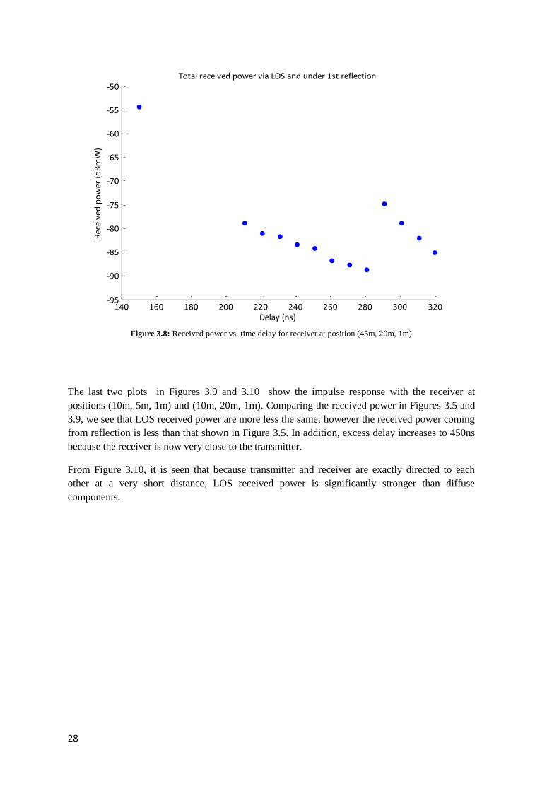
Figure 3.8: Received power vs. time delay for receiver at position (45m, 20m, 1m) .................... 28
Figure 3.9: Received power vs. time delay for receiver at position (10m, 5m, 1m) ...................... 29
Figure 3.10: Received power vs. time delay for receiver at position (10m, 20m, 1m) .................. 29
Figure 3.11: Upper perspective of a room with multiple reflection propagation ........................... 30
Figure 3.12: Received power vs. time delay for receiver at position (63m, 5m, 1m) .................... 31
Figure 3.13: Received power vs. time delay for receiver at position (45m,5m,1m) ...................... 31
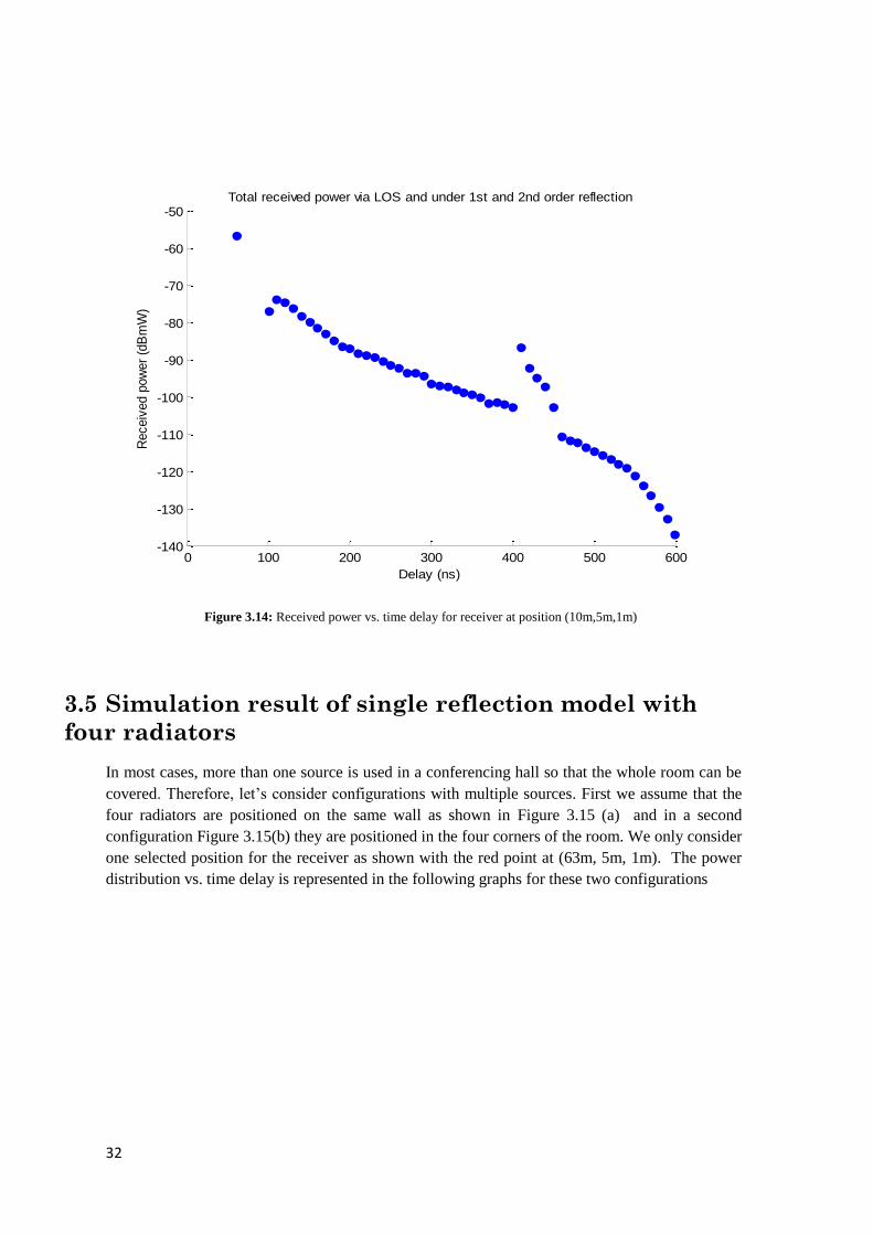
Figure 3.14: Received power vs. time delay for receiver at position (10m,5m,1m) ...................... 32
Figure 3.15: Two configurations of four radiators in the room ..................................................... 33
Figure 3.16: Received power vs. delay for the receiver shown in first conjuration ....................... 34
Figure 3.17: Received power vs. delay for the receiver shown in second configuration ............... 34
Figure 3.18: 30dB delay spread with LOS and N-LOS in single reflection channel model .......... 35
Figure 3.19: 40dB delay spread with LOS and N-LOS in single reflection channel model ......... 36
Figure 3.20: RMS delay spread with LOS and N-LOS in single reflection channel model ........... 36
Figure 3.21: 30dB delay spread with LOS and N-LOS in multi reflections channel model .......... 37
Figure 3.22: 40dB delay spread with LOS and N-LOS in multi reflections channel model .......... 37
Figure 3.23: RMS delay spread with LOS and N-LOS in multi reflections channel ..................... 38
Figure 4.1: A schematic of electrical-optical channel .................................................................... 39
Figure 4.2: A typical OW receiver ................................................................................................ 42
Figure 4.3: Circuit model and equivalent small circuit of a detector with low/ high impedance
amplifier ......................................................................................................................................... 45
Figure 4.4: Basic scheme of a detector with trans-impedance and its equivalent small circuit .... 46
Figure 4.5: Noise characteristic of a amplifier .............................................................................. 47
Figure 5.1: Radiant intensity of the LEDs vs. angle of half intensity, λ=870nm ........................... 50
Figure 5.2: Radiant intensity of the LED vs. angle of half intensity, λ=850nm ............................. 51
Figure 5.3: Maximum achievable bandwidth for selected Op-amps ............................................. 53
Figure 5.4: General measurement set up ........................................................................................ 54
Figure 5.5: LED driver circuit ........................................................................................................ 55
Figure 5.6: PIN diode driver circuit ............................................................................................... 56
Figure 5.7: Measurement set up ..................................................................................................... 57
Figure 5.8: Spectrum of the received signal ................................................................................... 57
Figure 6.1: Modulation scheme classification ................................................................................ 59
Figure 6.2: 16APSK constellation diagram .................................................................................... 61
Figure 6.3: Bandwidth efficiency vs. power efficiency ................................................................. 63
Figure 6.4: Bit error rate vs. bit to noise ratio ................................................................................ 64
Figure 7.1: Passing of baseband and MCM signal through a frequency selective channel ............ 68
Figure 7.2: FDM spectrum with 8 subcarriers and guard bands .................................................... 69
Figure 7.3: Spectrum of 8 equally modulated subcarriers in OFDM ............................................ 70
Figure 7.4: Comparison of spectral efficiency of FDM and OFDM .............................................. 70
Figure 7.5: Digital implementation of multi-cattier modulator. P/S denotes parallel-to-serial and
DAC digital-to-analogue conversion. ............................................................................................. 71
Figure 7.6: Generation of cyclic prefix guard interval ................................................................... 72
Figure 7.7: Simplified OFDM transmitter and receiver blocks ...................................................... 72
Figure 8.1: Raw data rate in different stages of transmitter ........................................................... 78
Figure 8.2: PAPR vs. number of subcarrier ................................................................................... 85

Figure 8.3: Power penalty vs. number of subcarrier ...................................................................... 85
List of Tables
Table 2.1: Comparison between radio and infrared properties for indoor wireless communication 8
Table 2.2: Comparison between wireless optical links ................................................................... 9
Table 4.1: Comparison between LED and LD ............................................................................... 40
Table 4.2: Interpretation of LED safety classification for optical sources .................................... 40
Table 4.3: Comparison of PIN and APD for wireless optical link ................................................. 43
Table 5.1: Light emitting diodes .................................................................................................... 49
Table 5.2: PIN diodes ..................................................................................................................... 52
Table 5.3: Summary of the OW components for target system ..................................................... 53
Table 6.1: Peak to average power ratio (PAPR) of several modulation schemes ......................... 65
Table 8.2: QPSK-OFDM parameters ............................................................................................. 83

xiii
Mathematical Symbol
roomA Area of room
ia Amplitude of i-th copy of received signal
RxA Detector area
B Frequency bandwidth
GB Guard band
availB Available bandwidth
effB Effective bandwidth
NB Sub-channel bandwidth
TB Total transmission bandwidth
cohB Coherence bandwidth
tC Sum of the photodiode junction and input capacitances
c Speed of light
detC Depletion capacitance of PIN diode
strayC Stray capacitance
FETC
Preamplifier capacitance
fC Feedback capacitance
Cf Compression factor
d Depletion layer width
dP Received power at reflector
dA Area of reflectors
ne Input voltage noise
Eb Energy per bit
E [.] Expectation
sf Sampling frequency
nf n-th subcarrier frequency
F Band limiting frequency of a filter
cf PIN diode cutoff frequency
3dBf Modulation bandwidth of LED
detFOV Detector field of view
refFOV Reflector field of view
f Measurement bandwidth
GBP Gain bandwidth product
( )kh Impulse response under k reflections
(0) ( )h t LOS impulse response
h(t) Multipath impulse response
H (f) Frequency impulse response
EQI Input equivalent noise
tnI Total noise current generated in a photo-detector

xiv
pI Photocurrent
DI Dark current
jnI Johnson noise
ni Input current noise
irI Irradiance
( )i t Received photo-current
k Current shot noise
Bk Boltzmann Constant
l Number of bits per symbol
pathM Number of multipath components
dataN Number of data subcarrier
pilotN Number of pilot subcarriers
nullN Number of null subcarriers
wdn Number of sample in sampling word
CPN Number of symbol in cyclic prefix
scN Number of sub-channel in multicarrier system
0N Noise power spectral density
eN
Number of reflecting element
ˆRxn Receiver orientation vector
ˆTxn Transmitter Orientation vector
ˆrefn Reflector orientation vector
Ln Lambert radiation index
dn
Lens index
nP Ambient light power
tP Transmitted optical power
P Radiated power from reflector
( )p Density function of the power delay profile
( )rp Power delay profile
rP Received power
q Electron charge
b OFDMR Data rate of an OFDM system
cR Coding rate
rR Raw bit rate per audio channel
TR Total data rate of 100 audio channel
Nr Factor of Nyquist filter
fR Feedback resistor
bR Data rate
LR Load resistance
r Distance

xv
Rx Receiver
sr Transmitter position vector
rect Rectangular function
Rr Receiver position vector
pR Responsivity of the detector
( )R radiation intensity
sR Symbol rate
s Surface of all reflectors
gT Guard interval
uT Useful symbol time
OFDMT Duration of an OFDM symbol
NT Symbol time in multicarrier system
mT Temperature
driftt Drift transit time
difft Diffusion time of carriers
RCt RC time constant
bT Bit duration
t Time
Tx Transmitter
RV Reverse voltage
X(t) Instantaneous optical power
RMS Root mean square (RMS) delay
max Maximum excess delay
m Mean excess delay
0 First-arrival delay
Excess time delay
rise Rise time
life Carrier lifetime
Bandwidth efficiency
1/2 Radiation half-angle
Angle between ˆRxn and ( )s Rr r
Direction angle of transmitter with respect to its normal vector
Dirac delta function
i Phase of i-th copy of received signal
ΔA Area of a reflecting element used in simulation
p Peak wavelength
Reflectivity
Traveling rate

xvi
Acronyms
AEL Allowable exposure limit
ACE Active constellation extension
APD Avalanche photodiodes
ASK Amplitude shift keying
BER Bit Error Rate
CE Constant Envelope
CPM Continuous phase modulation
CP Cyclic prefix
DQPSK Differential Quadrature Phase-Shift Keying
DC Direct current
DFT Discrete Fourier transform
DVB Digital Video Broadcasting
FCC Federal communication commission
FOV Field-of-view
FFT Fast Fourier transform
FDM Frequency Division Multiplexing
FSK Frequency shift keying
GMSK Gaussian minimum shift key
IM/DD Intensity modulation and direct detection
ISI Inter-symbol inference
IR Infrared radiation
IEC Electro-technical Commission
ICI Inter-carrier interference
LED Light Emitting Diode
LD Laser diodes
LOS Line of sight
MCM Multicarrier Modulation
MAPSK Amplitude and phase shift keying
MSK Minimum shift key
ML Maximum likelihood estimator
NLOS Non-Line-of- Sight
OFDM Equivalent power
PIN Positive-Intrinsic-Negative Diode
PSK Phase shift keying
PAPR Peak to average power radio
PSD Power spectral density
QAM Quadrature amplitude modulation
RS Reed Solomon
RF Radio frequency
RMS Root-mean-square
SFSK Sinusoidal frequency shift key
SNR Signal-to-noise ratio
SLM Selective mapping
TR Tone reservations
TIA Trans-impedance amplifier
WPAN Wireless personal area Network
ZP Zero-padding

xvii

1
1.
Introduction
Wireless communication systems have been evolving from one generation to the next and this is
mostly due to the increasing demand for higher data rates and capacity of the channel.
Also for clients of Bosch conferencing systems, there was a clear need for a high system capacity
which requires a high channel data rate. In that sense, the system can transmit more audio
channels with high quality. This master’s thesis is concerned with analysis of the feasible options
to increase the capacity of the system. However, evaluating any method starts with studying of the
requirements and the channel. In addition, it is necessary to look in more detail to challenges that
arose when high speed transmission is required.
1.1 Bosch Infrared language distribution system
The infrared language distribution system is used in conferences to distribute the interpreted
language of the speaker to participants. The two main reasons to use infrared are because the
distributed infrared signals cannot pass beyond the conference hall and there is huge unregulated
bandwidth at infrared frequency. This system consists of a transmitter, one or more radiators and
a number of receivers as shown in Figure 1.1.
Figure 1.1: Integrus system

2
The transmitter is the central element of the system. It receives inputs from either analog or digital
sources and modulates these signals onto multiple carriers. Then, this base band signal is
transmitted to infrared radiators mounted on the ceiling or walls in a conferencing hall. The output
of the radiator is intensity modulated infrared radiation. The radiators provide a reliable infrared
coverage from small meeting rooms up to very large conference halls.
Each delegate is equipped with a pocket receiver that has a lens to collect the infrared signal. The
signal is decoded into the interpretation language selected by the delegate and finally passed to
the headphone.
1.2 Technical characteristics of the system
The main infrared carrier of the radiators has an optical wavelength at 875nm. The baseband
transmission bandwidth between 2 and 8MHz is used; however, according to the standard for
infrared conferencing systems, only the bandwidth up to 6MHz is standardized.
The current system has up to 8 subcarriers with a bandwidth of 586.53 kHz each and uses a guard
band of 444 kHz, as shown in Figure 1.2. For each subcarrier, a single carrier transmission with
DQPSK modulation and a raised cosine pulse shaping with roll-off factor of 0.4 are used. This
results in a data rate of 837kb/s per carrier and a total data rate of 6.7 Mb/s for 32 audio channels.
Forward error correction with a (28, 24, 2) Reed-Solomon (RS) code and audio compression with
a factor of 2.6 are applied on each subcarrier.
Figure 1.2: Eight subcarriers in the assigned frequency band
Figure 1.3 and Figure 1.4 show the functional block diagrams of the transmitter and receiver. The
transmitter manages the following functions:
Audio Digitalization: each analogue audio channel is converted to a digital signal;
Audio compression: the digital signals are compressed in order to reduce the amount of
information for transmission. The compression factor is related to the required audio
quality.
Protocol generation and framing
Forward error correction: it is applied to protect the audio and data information from
transmission error using RS code of (28, 24, 2)
Synchronization insertion: to detect the start of the data.
DQPSK modulation: the symbol information is encoded as the phase change from one
symbol period to the next rather than as an absolute phase.
Digital to analog convertor

3
The front end of the transmitter uses intensity modulation by modulating the output power
of infrared LEDs.
And the receiver manages the inverse of all the mentioned functions except audio de-
compression.
Figure 1.3: Transmitter Architecture
Figure1.4: Receiver Architecture

4
1.3 Goal of the thesis
The overall goal of this thesis is to investigate the feasibility of increasing the data rate of the
Bosch infrared language distribution system. The number of audio channels to be supported by
new system shall be at least 100. In that case, the system shall have a transmission rate of at least
20Mb/s. Therefore, this thesis provides an insight on the performance of various modulation
techniques for the system with which the requirement is met. In that context, two main questions
are handled
What are the limits for transmission rate in an intensity modulation and direct detection (IM/DD)
channel?
How and to what extent can these limitations affect the design choices in practice?
The transmission data rate of wireless communication system is strongly affected by multipath
propagation. The delay of the channel causes stretching of the input signal which creates signal
distortion referred to as inter-symbol inference (ISI). Therefore, it is necessary to investigate the
behaviour of the channel.
Another limiting factor is created in the design of the system; the opto-electrical components used
in the transmitter and receiver have speed limitations. For example the photo-detector is the main
component in limiting the bandwidth of the system.
To answer these questions, this thesis investigates the following subjects
Modelling of the optical wireless channel to determine the effect of the multipath on the
bandwidth limitation (channel delay spread).
Bandwidth limitation factors in the transmitter and receiver front-end designs are
determined.
Analyze several modulation techniques such as single and multicarrier modulations and
select the appropriate scheme that fits with channel characteristics and meets the
requirement.
Identifying the issues related to the link budget analysis of the chosen modulation.
1.4 Outline of the thesis
This thesis consists of eight technical chapters with the main contributions in the chapters 3, 5 and
8. In the following the content of all chapters is outlined
Chapter 2 begins with a comparison between radio frequency (RF) and infrared (IR) radiation. It
continues with a short review of basic optical links and fundamentals of propagation in the optical
wireless channel. Furthermore, a mathematical channel model for line of sight (LOS) and diffuse
links is discussed. In the last section the noise sources of an optical channel is discussed.
Chapter 3 consists of a set of simulation model for optical wireless channel to determine delay
spread and root-mean-square (RMS) delay.

5
Chapter 4 defines the opto-electrical components in the front-end of the system. The aim of this
chapter is to determine the factors which limit the bandwidth of the system.
Chapter 5 discusses the characteristics of the new opto-electrical components available in the
market. The aim of this chapter is to determine the possibility of increasing the bandwidth by
means of applying these new components. It is included a simple measurement set up to verify the
feasibility of supporting large bandwidth.
Chapter 6 briefly describes different digital modulation techniques and compares them in terms of
power, bandwidth efficiency and bit error probability.
Chapter 7 describes the concept of multipath channel and introduces multicarrier modulation as a
promising technique to handle multipath dispersion. A mathematical model of the Orthogonal
Frequency Division Multiplexing (OFDM) is presented and it is followed by discussing the
challenges in designing an OFDM system.
Chapter 8 focuses on theoretical calculation of the total transmission rate of the system
considering single and multicarrier modulation schemes as discussed in previous chapters. Also,
the link budget analysis of these approaches is compared.
Chapter 9 summarizes the main results and offers an outlook for future work.
7
2.
Indoor wireless infrared
communication
This chapter discusses advantages and disadvantages of IR over RF. A short
review of basic optical links and fundamentals of pr opagation in optical
channels will be given. A mathematical model for evaluating the impulse
response of the infrared channel with as many reflections as required will
be discussed. In the last section, the noise source of an optical channel will
be discussed as well.
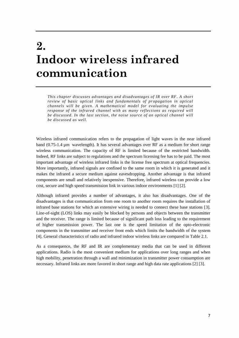
Wireless infrared communication refers to the propagation of light waves in the near infrared
band (0.75-1.4 µm wavelength). It has several advantages over RF as a medium for short range
wireless communication. The capacity of RF is limited because of the restricted bandwidth.
Indeed, RF links are subject to regulations and the spectrum licensing fee has to be paid. The most
important advantage of wireless infrared links is the license free spectrum at optical frequencies.
More importantly, infrared signals are confined to the same room in which it is generated and it
makes the infrared a secure medium against eavesdropping. Another advantage is that infrared
components are small and relatively inexpensive. Therefore, infrared wireless can provide a low
cost, secure and high speed transmission link in various indoor environments [1] [2].
Although infrared provides a number of advantages, it also has disadvantages. One of the
disadvantages is that communication from one room to another room requires the installation of
infrared base stations for which an extensive wiring is needed to connect these base stations [3].
Line-of-sight (LOS) links may easily be blocked by persons and objects between the transmitter
and the receiver. The range is limited because of significant path loss leading to the requirement
of higher transmission power. The last one is the speed limitation of the opto-electronic
components in the transmitter and receiver front ends which limits the bandwidth of the system
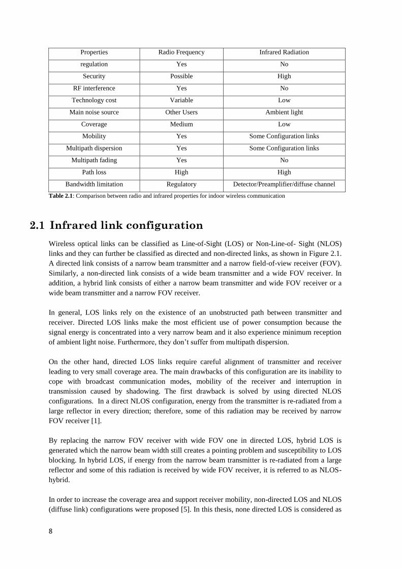
[4]. General characteristics of radio and infrared indoor wireless links are compared in Table 2.1.
As a consequence, the RF and IR are complementary media that can be used in different
applications. Radio is the most convenient medium for applications over long ranges and when
high mobility, penetration through a wall and minimization in transmitter power consumption are
necessary. Infrared links are more favored in short range and high data rate applications [2] [3].
8
Properties Radio Frequency Infrared Radiation
regulation Yes No
Security Possible High
RF interference Yes No
Technology cost Variable Low
Main noise source Other Users Ambient light
Coverage Medium Low
Mobility Yes Some Configuration links
Multipath dispersion Yes Some Configuration links
Multipath fading Yes No
Path loss High High
Bandwidth limitation Regulatory Detector/Preamplifier/diffuse channel
Table 2.1: Comparison between radio and infrared properties for indoor wireless communication
2.1 Infrared link configuration
Wireless optical links can be classified as Line-of-Sight (LOS) or Non-Line-of- Sight (NLOS)
links and they can further be classified as directed and non-directed links, as shown in Figure 2.1.
A directed link consists of a narrow beam transmitter and a narrow field-of-view receiver (FOV).
Similarly, a non-directed link consists of a wide beam transmitter and a wide FOV receiver. In
addition, a hybrid link consists of either a narrow beam transmitter and wide FOV receiver or a
wide beam transmitter and a narrow FOV receiver.
In general, LOS links rely on the existence of an unobstructed path between transmitter and
receiver. Directed LOS links make the most efficient use of power consumption because the
signal energy is concentrated into a very narrow beam and it also experience minimum reception
of ambient light noise. Furthermore, they don’t suffer from multipath dispersion.
On the other hand, directed LOS links require careful alignment of transmitter and receiver
leading to very small coverage area. The main drawbacks of this configuration are its inability to
cope with broadcast communication modes, mobility of the receiver and interruption in
transmission caused by shadowing. The first drawback is solved by using directed NLOS
configurations. In a direct NLOS configuration, energy from the transmitter is re-radiated from a
large reflector in every direction; therefore, some of this radiation may be received by narrow
FOV receiver [1].
By replacing the narrow FOV receiver with wide FOV one in directed LOS, hybrid LOS is
generated which the narrow beam width still creates a pointing problem and susceptibility to LOS
blocking. In hybrid LOS, if energy from the narrow beam transmitter is re-radiated from a large
reflector and some of this radiation is received by wide FOV receiver, it is referred to as NLOS-
hybrid.
In order to increase the coverage area and support receiver mobility, non-directed LOS and NLOS
(diffuse link) configurations were proposed [5]. In this thesis, none directed LOS is considered as

9
optical link configuration. In such link, LOS and diffuse signal components are simultaneously
presented at the receiver. Non-direct LOS makes better use of signal power than the diffuse like,
but it requires that the LOS path be uninterrupted. Diffuse links rely on the reflected paths from
objects in a room and operate without LOS. Because a diffuse transmitter does not need to be
aimed at the receiver, it provides a wide degree of mobility which is the most convenient
configuration from the user point of view. Therefore, a diffuse link is very robust against
shadowing and no tight alignment is required for users. On the other hand, a diffuse system
suffers from very high signal attenuation, so a large optical transmitted power is required. In
addition, multipath reflection in diffuse links can cause inter-symbol-interference (ISI) [2].
Besides, the received optical power in NLOS links depends on properties of the room such as size
and reflection coefficients of reflectors as well as orientation angles of transmitter and receiver.
Table 2.2 summarizes the characteristics of directed LOS and diffuse configurations.
Figure 2.1: Configuration for wireless optical links [1]
Characteristic Directed LOS Link Diffuse Link
Data rate High Low-Moderate
Pointing required Yes No
Immunity to Blocking Low High
Mobility Low High
Complexity of Optics Low Low-Moderate
Ambient light Rejection High Low
Multipath Distortion No High
Path Loss Low High
Table 2.2: Comparison between wireless optical links [3]

10
In order to combine the mobility of the diffuse link and high speed capability of the LOS link, the
multi-spot diffusing approach was proposed in [2]. In this approach, a diffuse transmitter is
replaced by a quasi-diffuse transmitter which utilizes multiple narrow beams pointed in different
directions which reduces the path loss. The reason is the narrow beams experience little path loss
traveling from transmitter to receiver. Also, a single element receiver is replaced with an imaging
light concentrator and a segmented photo-detector which can reduce received ambient light noise
and multipath distortion [2].
2.2 Propagation in optical wireless channel
In optical communication, the most viable modulation is intensity modulation with direct
detection (IM/DD) in which the information is modulated onto the intensity of the optical signal.
Because of the intensity modulation, the channel input signal X (t) is instantaneous optical power
and it must be positive. The average power of the transmitted optical signal is given by [3]
1
lim ( )2
T
tT
T
P X t dtT
(2.1)
The optical signals between transmitter and receiver in a wireless non-directed NLOS channel
travel different paths and experience path loss and propagation delay. If a signal is transmitted
over a multipath channel then the received signal is the superposition of attenuated and delayed
copies of the transmitted signal which causes constructive and destructive interference of original
signal [7].
The resulting effect of the multipath propagation of an optical signal is similar as observed for a
RF signal. Consequently, multipath reflections create time dispersion of the received signal
(multipath dispersion) and variation in amplitude of the received signal which is referred to as
multipath fading.
One of the major differences between RF and IR systems is the size of the receiving antenna
relative to the wavelength of the received signal. Typical photo-detector dimensions are thousand
of the wavelength. Therefore, the total received power by a direct detection receiver may remain
the same as the receiver changes its position by thousands of wavelength. In radio, as the receiver
changes its position by a fraction of the wavelength, the channel properties change drastically [8].
The large detector area leads to efficient diversity which reduces the effect of multipath fading
and simplifies the link design [3].
Multipath dispersion is, however, very much present in optical wireless channel. In the following
section, the parameters that characterize propagation delay mechanism are presented.
11
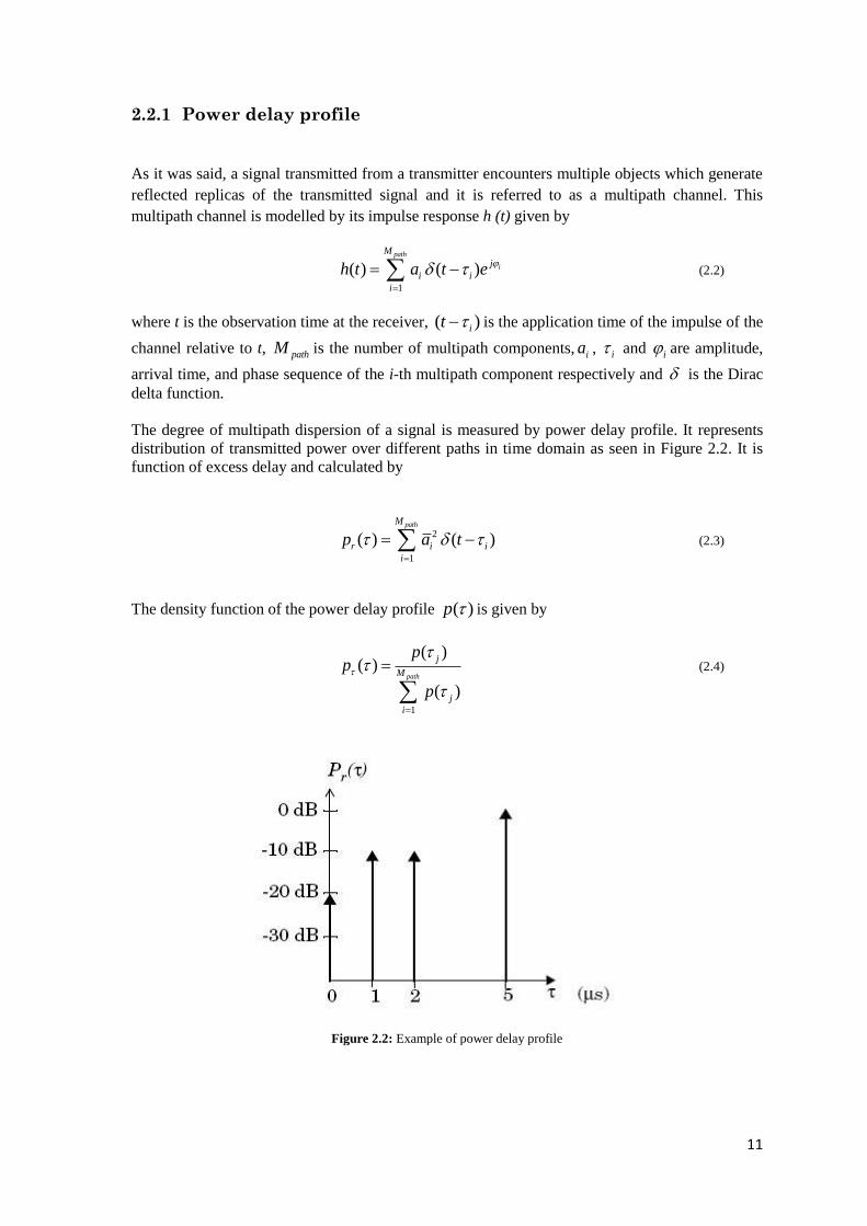
2.2.1 Power delay profile
As it was said, a signal transmitted from a transmitter encounters multiple objects which generate
reflected replicas of the transmitted signal and it is referred to as a multipath channel. This
multipath channel is modelled by its impulse response h (t) given by
1
( ) ( )path
i
M
j
i i
i
h t a t e
(2.2)
where t is the observation time at the receiver, ( )it is the application time of the impulse of the
channel relative to t, pathM is the number of multipath components, ia , i and i are amplitude,
arrival time, and phase sequence of the i-th multipath component respectively and is the Dirac
delta function.
The degree of multipath dispersion of a signal is measured by power delay profile. It represents
distribution of transmitted power over different paths in time domain as seen in Figure 2.2. It is
function of excess delay and calculated by
2
1
( ) ( )pathM
r i i
i
p a t
(2.3)
The density function of the power delay profile ( )p is given by
1
( )( )
( )path
j
M
j
i
pp
p
(2.4)
Figure 2.2: Example of power delay profile
12
2.2.2 Time delay spread
When a transmitted signal arrives at receiver through multipath propagation, it causes signal
dispersion in time. There are some parameters which can quantify the multipath channel in time
domain. The mean excess delay, RMS delay spread, and excess delay spread are multipath
channel parameters that can be determined from a power delay profile and they are explained
below
First-arrival delay ( 0 ) is time delay corresponding to the arrival of the first transmitted signal at
the receiver. It acts as a reference and any delay longer than this is called an excess delay.
Mean excess delay ( m ) is the first moment of power delay profile with respect to the first delay.
Maximum excess delay ( max ) is an excess delay that is measured with respect to specific power
level called the threshold of the signal. When the received signal is less than this threshold, it is
not considered.
Root mean square (RMS) delay ( RMS ) is square root of the second moment of the power delay
profile. It is standard deviation about the mean excess delay.
RMS delay spread is a good measure of channel time’s dispersion and shows an indication of
nature of ISI in the received signal. It is expressed by the impulse response h (t) and the multipath
mean delay (m ) as
1/22 2 2
2 2
( ) ( ) ( ), [ ]
( ) ( )
m
RMS m
t h t dt th t dts
h t dt h t dt
(2.5)
To avoid ISI, transmitted signal requires having a symbol period (sT ) that is large relative to
RMS delay ( ( )s RMST . Conversely, if the symbol period is less than RMS , the signal experience
significant ISI. Thus, the maximum data rate of the system is limited by RMS as 1/10s RMSR
where sR is the symbol rate [9].
2.2.3 Coherence Bandwidth
Multipath dispersion can also be characterized in the frequency domain by coherence bandwidth
( cohB ). Coherence bandwidth is the frequency range over which the frequency components of a
signal experience correlated amplitude fading [9]. The relationship between cohB and RMS is
given by
1
[ ]2
coh
RMS
B Hz
(2.6)
Equivalently, to avoid ISI, the bandwidth of the signal must be much smaller than the coherence
bandwidth ( cohB B ). Then the fading across the entire signal bandwidth is roughly equal
13
which is referred to as flat fading. On the other hand, if cohB B then the amplitude values of
different frequency components of a signal vary differently across the signal bandwidth which is
referred to as frequency selectivity resulting to ISI [9].
2.2.4 Doppler Effect
For a fixed transmitter, receiver and reflectors, the optical channel impulse response is stationary.
When these objects are moving relative to each other, then the frequency of the received signal is
not the same as that at the source due to Doppler effect. It means when objects are approaching
each other, the frequency of the received signal is higher and when they are moving away, it is
lower than source.
Here, we ignore Doppler effect for the optical channel because the channel varies very slowly and
it can be considered as time invariant [1], [3]. Therefore, if X (t) is the instantaneous output power
of the source, the received electrical current after detection in a noiseless multipath optical
channel is given by
( ) ( ) ( )pi t R X t h t
(2.7)
where, indicates convolution and pR [A/W] denotes the responsivity of the detector which is
conversion factor at the receiver.
2.3 Optical wireless channel model
Many researchers have modelled the indoor infrared wireless channel to determine the delay
spread and distribution of power throughout a room.
Gfeller et al. [5] introduced the idea of using infrared for indoor wireless communications. He
studied various physical channel properties, namely, the reflection properties of several materials,
bandwidth limitation due to multipath dispersion, ambient noise and distribution of diffuse optical
radiation. In the paper, they suggested the Lambertian pattern as model for the reflections from
the surface which will be explained in 2.3.1.
Barry et al. [1] proposed a general simulation method for evaluating characterization of the
impulse response of an indoor optical channel. The model can compute the impulse response for
as many reflections as required. Based on his model, the room is divided into numerous small
reflecting elements. It is a recursive model so that to find the impulse response of the thk
reflections, the impulse response of ( 1)thk reflections and LOS are required. One drawback of
this method is its long simulation time.
Lopez-Hernandez et al. [10] proposed a novel algorithm called the “DUSTIN algorithm” for
calculating the impulse response of the IR wireless indoor channels. The method is fast in
computing the impulse response and it is split into three stages: initialization, wall processing and
calculating of the photo diode response.

14
Lopez-Hernandez et al. [11] also developed a method to find the impulse response by using
Monte Carlo analysis. It does not only evaluate the Lambertian but also specular reflections.
Carruthers et al. [12] described an iterative method for the estimation of the impulse response of
the wireless infrared channels. This method can consider any order of reflections. Complex
reflection environments with all types of obstructions, shadowing effects and related effects can
be modeled. It can perform more accurately and efficiently than the recursive method used by
Barry et al [1].
Cipriano et al. [13] developed a computationally efficient algorithm for simulation of the wireless
infrared channel. Two new procedures, namely, Time Delay Agglutination and Time and Space
Indexed Tables are defined to increase the efficiency of the simulation of the impulse response for
the indoor wireless optical channel. The results presented in this paper show good agreement with
those already published and verified experimentally [1] [8].
Large experimental measurements of indoor IR channel were performed at the University of
Ottawa [8] over a 40 MHz band for many different configurations. They investigated impact of
receiver rotation and shadowing on the properties of indoor infrared channels. The results
demonstrate the effect of elevation angle of the receiver on path loss, correlation between the
channel delay spread and path loss for LOS and diffuse configurations.
In this thesis, optical wireless channel model proposed by John Barry [1] is discussed and used for
simulation because of good prediction of the channel properties. Other available methods are a
more or less modified version of this model.
In general the impulse response of the non directed LOS channel consists of two components,
discrete Dirac-pulse due to the LOS and a continuous signal due to contributions of diffuse
reflections. Figure 2.3 illustrates a sketch of the channel impulse response model.
Figure2.3: Sketch of the impulse response
15
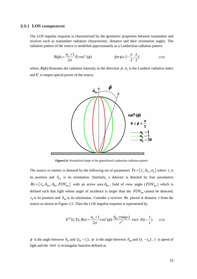
2.3.1 LOS component
The LOS impulse response is characterized by the geometric properties between transmitter and
receiver such as transmitter radiation characteristic, distance and their orientation angles. The
radiation pattern of the source is modelled approximately as a Lambertian radiation pattern
1
( ) cos ( ) [ , ]2 2 2
LnLt
nR P for
(2.8)
where, ( )R illustrates the radiation intensity in the direction , Ln is the Lambert radiation index
and tP is output optical power of the source.
Figure2.4: Normalized shape of the generalized Lambertian radiation pattern
The source or emitter is denoted by the following set of parameters ˆ, ,s Tx LTx r n n where sr is
its position and ˆTxn is its orientation. Similarly, a detector is denoted by four parameters
detˆ, , ,R Rx RxRx r n A FOV with an active area RxA , field of view angle ( detFOV ) which is
defined such that light whose angle of incidence is larger than the detFOV cannot be detected,
Rr is its position and ˆRxn is its orientation. Consider a receiver Rx placed at distance r from the
source as shown in Figure 2.5. Then the LOS impulse response is represented by
(0)
2
cos( )1( , , ) cos ( ) ( )
2
n RxLAn r
h t Tx Rx rect tr c
(2.9)
is the angle between ˆTxn and ( )R sr r , is the angle between ˆ
Rxn and ( )s Rr r , c is speed of
light and the rect is rectangular function defined as
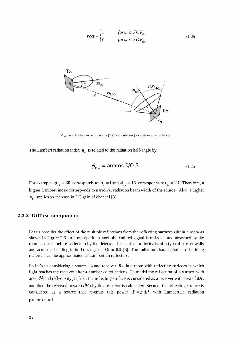
16
det
det
1
0
for FOVrect
for FOV
(2.10)
Figure 2.5: Geometry of source (Tx) and detector (Rx) without reflectors [7]
The Lambert radiation index Ln is related to the radiation half-angle by
1/2 arccos 0.5Ln (2.11)
For example, 1/2 60 corresponds to 1Ln and
1/2 15 corresponds to 20Ln . Therefore, a
higher Lambert index corresponds to narrower radiation beam width of the source. Also, a higher
Ln implies an increase in DC gain of channel [3].
2.3.2 Diffuse component
Let us consider the effect of the multiple reflections from the reflecting surfaces within a room as
shown in Figure 2.6. In a multipath channel, the emitted signal is reflected and absorbed by the
room surfaces before collection by the detector. The surface reflectivity of a typical plaster walls
and acoustical ceiling is in the range of 0.6 to 0.9 [3]. The radiation characteristics of building
materials can be approximated as Lambertian reflectors.
So let’s us considering a source Tx and receiver Rx in a room with reflecting surfaces in which
light reaches the receiver after a number of reflections. To model the reflection of a surface with
area dA and reflectivity , first, the reflecting surface is considered as a receiver with area of dA ,
and then the received power ( dP ) by this reflector is calculated. Second, the reflecting surface is
considered as a source that re-emits this power P dP with Lambertian radiation
pattern 1Ln .

17
Figure2.6: Multiple reflections propagation model
Therefore, the impulse response of the light undergoing k reflections can be written as
0
( , , ) ( , , )k
kh t Tx Rx h t Tx Rx
(2.12)
The LOS impulse response is represented by (0) ( )h t while the higher order reflections are
calculated by a recursive algorithm:
( ) (0) 1ˆ ˆ( , , ) ( ; ,{ , , , }) ( ;{ , , 1}, )k k
p ref ref p ref L
s
h t Tx Rx h t Tx r n FOV dA h t r n n Rx (2.13)
where, ˆrefn is orientation vector of the reflecting surface at position
pr and integration is
performed over the surface ( s ) of all reflectors. Substituting Eq.2.9 in Eq.2.13 and performing
convolution result in:
( ) 1
2
1 cos( )cos ( )ˆ( , , ) ( / ;{ , , 1}, )
2
Lnk kL
p ref L
s
nh t Tx Rx rect h t r c r n n Rx dA
r
(2.14)

18
2.4 Noise sources in optical wireless channel
In infrared systems, the noise is generated by internal and external components at the receiver
front end. The internal noise is generated in the receiver is from front-end electronic components
such as resistor, diode and transistor which referred to as thermal noise. The important source of
noise in the optical channel is the background light referred to as external source of noise.
Generally, the background light is presented as a mixture of light coming from the sun,
incandescent and fluorescent lighting. The spectral power density of different sources including
Light Emitting diode (LED), photo-detector (PD) and laser diode (LD) are shown in Figure 2.7.
Figure2.7: Optical power spectra of common ambient infrared sources[7]
The natural light coming from sun is practically stationary whereas the light produced by artificial
sources exhibits fast fluctuations in time. Hence, both natural and artificial sources produce a
certain amount of background optical power impinging to the photo-detector. Because of this
background optical power, a high level of shot noise current is generated in the photo-detector and
increases the noise floor and decreases the sensitivity of an optical receiver. In addition,
fluorescent artificial sources generate interference at frequencies of hundreds of kilohertz [7]. The
shot noise is essentially white Gaussian noise, given by
2 , ( )sn p nI qR P A (2.15)
where, 191.6 10 [ ]q As denotes the electron charge, nP
is the ambient light power (W) and
pR is (A/w) responsivity of photo-detector.

19
In order to suppress the background noise, it is desired to use a narrow beam detector and day
light filter before detection. The use of an optical filter reduces the amount of undesirable optical
power producing shot noise at the receiver. It also provides an efficient reduction in the
interference generated by artificial lighting. Therefore, the actual average photocurrent coming
from background radiation depends on the receiver design [14] [15]. As mentioned, apart from
shot noise, there is thermal noise which also contributes to the link performance degradation. The
level of thermal noise depends on the receiver preamplifier circuit design. A more detailed
analysis of thermal noise is given in Chapter 4 where the receiver front-end is discussed.
21
3.
Simulation model for the
indoor infrared channel
In this chapter a simulation model is described to determine the delay spread and RMS
delay spread of the optical channel in a room of arbitrary dimension. The investigation
shows that the optical wireless channel varies for different scenarios and first order
reflections have the most effect on the characteristics of the channel.
As it is mentioned in chapter 2, a simulation model of the indoor infrared channel has been
introduced by Gfeller et al [5]. Barry et al [1] presented a general computer simulation method for
infrared channel characterization. In this thesis, based on the mathematical model introduced in
chapter 2, we present a recursive method in order to calculate the channel delay spread of an
arbitrary room with Lambertian reflectors as well as channel path loss. This method can account
for multiple reflections of the first and second order which evaluates the effect of multipath
dispersion. It can be enhanced for any order of reflections but as we will see, considering first and
second order reflections is sufficient.
This simulation model can benefit significantly the system design since the delay spread and RMS
delay spread can be calculated from the impulse response by Eq. (2.5). In future investigations, it
is necessary to verify the accuracy of this simulation model with experimental measurement of the
optical multipath channel.
In the following sections we describe the recursive algorithm and three different scenarios that
have been simulated. The first scenario is to consider a single reflection channel with only one
source, and then multiple reflections channel with one source. The last scenario is to model the
single reflection channel with four sources installed in the room.
3.1 Channel simulation model
Given a source and receiver with vectors Tx and Rx as defined in chapter 2 in a room with
reflectors, light can reach a detector after any number of reflections. The reflectors are assumed to
be ideal Lambertian because the experimental measurements have shown that many materials are
well approximated as Lambertian reflectors [1]. To be reminded, the radiation intensity pattern of
a reflector is given by Eq. (2.8). Eq. (2.12) is the major theoretical approach on which the
simulation model is based to find the k-bounce impulse response.

22
To implement the integral in Eq. (2.12), the reflecting surfaces are subdivided into small
reflecting elements (iE ) with area of A . Therefore, the impulse response can be written as a
summation with
( ) 1
21
cos( )cos ( )1ˆ( , , ) ( / ;{ , , 1}, )
2
Le nNk kiL
p ref L
i
nh t Tx Rx rect h t r c r n n Rx A
r
(3.1)
where i represents the i-th reflecting element and eN is total number of reflecting elements.
The flowchart which implements this procedure is shown in Figure 3.1. In general, the required
input parameters are in terms of transmitter and receiver vectors as explained in 2.3.1, transmitted
optical power ( tP ), eN reflecting elements, room size ( roomA ) and reflectivity (ρ) of walls. Walls
of the room are subdivided into a large set of reflectors with very small areas A . LOS received
power and its arrival time is calculated. To implement Eq. (3.1) to determine diffuse received
power, two computations are performed where one computation is defined as the calculation of
differential power and delay from a source to a reflecting element and the second computation is
defined as calculation of the received power and delay from the reflecting element to the detector.
The received power and delay of different paths are collected and by searching through the arrival
times of the signal, the maximum and minimum arrival times are determined. The first arrival
delay corresponds to the LOS received signal and in order to calculate received power via the
reflections, continuous function of time observed up to the maximum arrival time is subdivided
into the bins with width of t and the power received within each time bin is sum up.
Figure 3.1: Algorithm implemented to simulate impulse response of an infrared channel
23
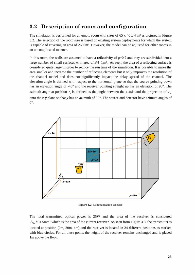
3.2 Description of room and configuration
The simulation is performed for an empty room with sizes of 65 x 40 x 4 m³ as pictured in Figure
3.2. The selection of the room size is based on existing system deployments for which the system
is capable of covering an area of 2600m². However; the model can be adjusted for other rooms in
an uncomplicated manner.
In this room, the walls are assumed to have a reflectivity of ρ=0.7 and they are subdivided into a
large number of small surfaces with area of ΔA=1m². As seen, the area of a reflecting surface is
considered quite large in order to reduce the run time of the simulation. It is possible to make the
area smaller and increase the number of reflecting elements but it only improves the resolution of
the channel model and does not significantly impact the delay spread of the channel. The
elevation angle is defined with respect to the horizontal plane so that the source pointing down
has an elevation angle of -45° and the receiver pointing straight up has an elevation of 90°. The
azimuth angle at position pr is defined as the angle between the x axis and the projection of pr
onto the x-y plane so that y has an azimuth of 90°. The source and detector have azimuth angles of
0°.
Figure 3.2: Communication scenario
The total transmitted optical power is 25W and the area of the receiver is considered
RxA =31.5mm² which is the area of the current receiver. As seen from Figure 3.3, the transmitter is
located at position (0m, 20m, 4m) and the receiver is located in 24 different positions as marked
with blue circles. For all these points the height of the receiver remains unchanged and is placed
1m above the floor.
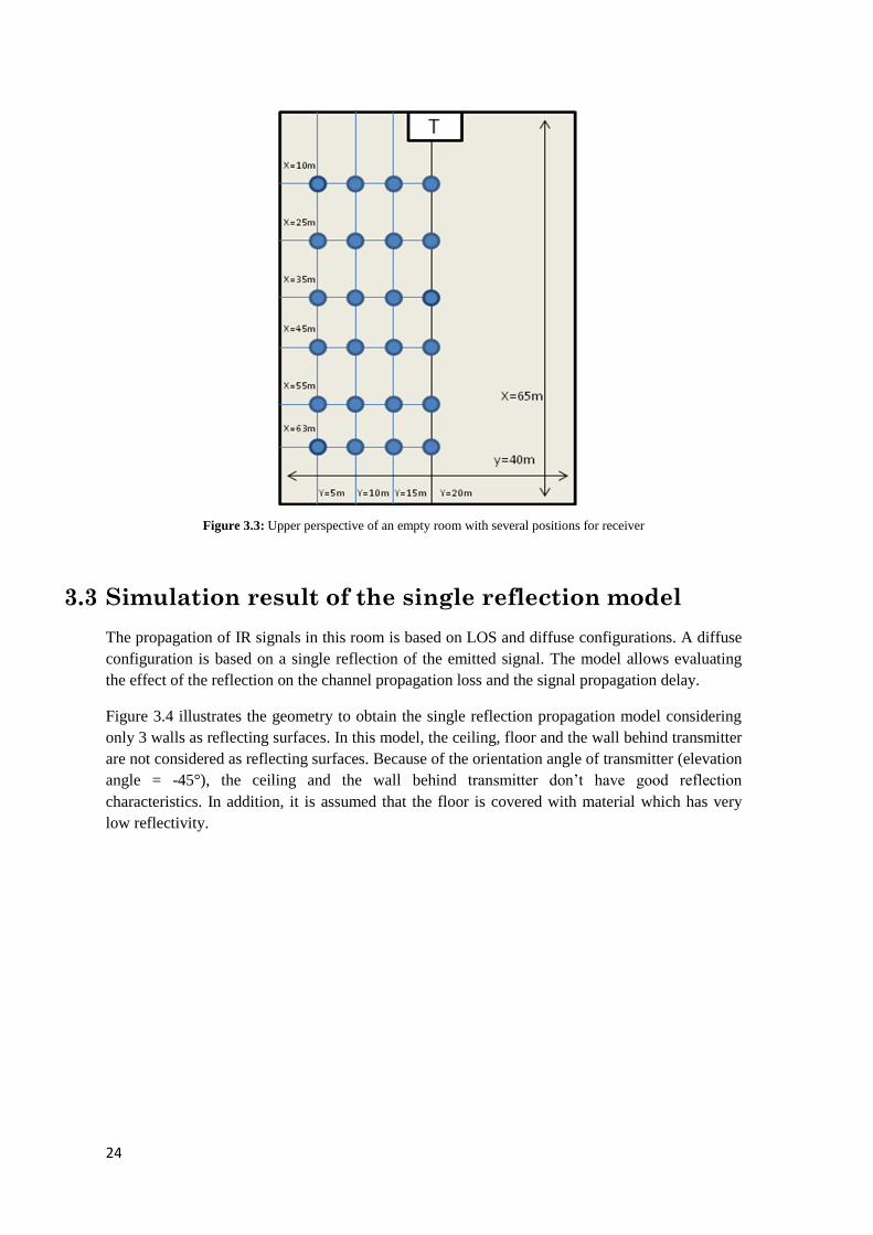
24
Figure 3.3: Upper perspective of an empty room with several positions for receiver
3.3 Simulation result of the single reflection model
The propagation of IR signals in this room is based on LOS and diffuse configurations. A diffuse
configuration is based on a single reflection of the emitted signal. The model allows evaluating
the effect of the reflection on the channel propagation loss and the signal propagation delay.
Figure 3.4 illustrates the geometry to obtain the single reflection propagation model considering
only 3 walls as reflecting surfaces. In this model, the ceiling, floor and the wall behind transmitter
are not considered as reflecting surfaces. Because of the orientation angle of transmitter (elevation
angle = -45°), the ceiling and the wall behind transmitter don’t have good reflection
characteristics. In addition, it is assumed that the floor is covered with material which has very
low reflectivity.

25
Figure 3.4: Upper perspective of a room for single reflection propagation model
In Figures 3.5 and 3.6 an illustrations of the impulse response are given when the receiver is
located at positions (63m, 5m, 1m) and (63m, 20m, 1m). In this case, the distance between
transmitter and receiver becomes very large and little optical power is collected.
The first point on the plots indicates LOS received power which is about -60dBm at a delay of
216ns in the first plot. It is interesting to be noted that the power received via reflections is more
than LOS power at arrival time of 236ns. As seen, for arrivals afterwards, there is an
exponentially decay in the power.
The same behavior is seen when the receiver is moved to the middle of the room at position (63m,
20m, 1m). The LOS received power slightly increases and, due to the location of the receiver, the
excess delay is shorter compared to the first plot.

26
200 220 240 260 280 300 320 340-95
-90
-85
-80
-75
-70
-65
-60
-55
Delay (ns)
Rec
eive
d p
ow
er (
dB
mW
)
Total received power via LOS and under 1st reflection
Figure 3.5: Received power vs. time delay for receiver at position (63m, 5m, 1m)
200 210 220 230 240 250 260 270 280 290 300-95
-90
-85
-80
-75
-70
-65
-60
-55
Delay (ns)
Rec
eive
d p
ow
er (
dB
mW
)
Total received power via LOS and under 1st reflection
Figure 3.6: Received power vs. time delay for receiver at position (63m, 20m, 1m)

27
Figure 3.7 and 3.8 show the impulse responses of the channel when the receiver is located at
positions (45m, 5m,1m) and (45m, 20m,1m). Clearly from the first plot, the LOS received power
increases to -58dBm at a shorter delay of 158ns compared to the previous result. The LOS arrival
time is shorter because the receiver is now close to the transmitter. The received power coming
from the nearby reflectors decreases exponentially up to a time delay of 282ns. Afterwards, there
are strong reflections with large excess delay at 292ns due to reflection from far away reflectors
and result in a cluster of reflections.
This cluster contains multiple reflections from the same transmitted signal arriving at the receiver
with different time delay and with different amplitudes, but from the same general direction. Here
since the receiver is almost in the middle of the room, the reflecting element located at position x
= 65m on the back wall cause strong reflections with large excess delay because of their good
orientation angles with respect to the transmitter. In addition, the larger the room being modeled
the more clusters appear in the model resulting in a large RMS delay spread.
In Figure 3.8, the receiver moves to the middle of the room and the effect of LOS dominates any
reflection paths. LOS received power is about -54dBm at a delay of 150ns. The same clustering
effect also occurs here; however excess time delay is limited to 320ns which is less compared to
the situation that the receiver is at left side of the room.
150 200 250 300 350 400-95
-90
-85
-80
-75
-70
-65
-60
-55
Delay (ns)
Rec
eive
d p
ow
er (
dB
mW
)
Total received power via LOS and under 1st reflection
Figure 3.7: Received power vs. time delay for receiver at position (45m, 5m, 1m)
28
140 160 180 200 220 240 260 280 300 320-95
-90
-85
-80
-75
-70
-65
-60
-55
-50
Delay (ns)
Rec
eive
d p
ow
er (
dB
mW
)
Total received power via LOS and under 1st reflection
Figure 3.8: Received power vs. time delay for receiver at position (45m, 20m, 1m)
The last two plots in Figures 3.9 and 3.10 show the impulse response with the receiver at
positions (10m, 5m, 1m) and (10m, 20m, 1m). Comparing the received power in Figures 3.5 and
3.9, we see that LOS received power are more less the same; however the received power coming
from reflection is less than that shown in Figure 3.5. In addition, excess delay increases to 450ns
because the receiver is now very close to the transmitter.
From Figure 3.10, it is seen that because transmitter and receiver are exactly directed to each
other at a very short distance, LOS received power is significantly stronger than diffuse
components.

29
50 100 150 200 250 300 350 400-110
-100
-90
-80
-70
-60
-50
Delay (ns)
Rec
eive
d p
ow
er (
dB
mW
)
Total received power via LOS and under 1st reflection
Figure 3.9: Received power vs. time delay for receiver at position (10m, 5m, 1m)
0 50 100 150 200 250 300 350 400 450-110
-100
-90
-80
-70
-60
-50
-40
-30
-20
Delay (ns)
Rec
eive
d p
ow
er (
dB
mW
)
Total received power via LOS and under 1st reflection
Figure 3.10: Received power vs. time delay for receiver at position (10m, 20m, 1m)

30
3.4 Simulation result of the multiple reflections model
In this model, room, transmitter and receiver configurations remain the same and the only new
consideration is that also second order reflections are included in the detected signal. In this
model, all the walls including the ceiling and the wall behind transmitter are taken as reflectors
but the floor is not considered.
The impulse response of only three receiver positions is represented here to evaluate the effect of
second order reflections. It has to be mentioned that we limited the number of second reflections
such that the computation can be performed in a reasonable amount of time. In that sense, the
following scenario as shown in Figure 3.11 is defined. The same algorithm shown in Figure 3.1 is
applied to calculate the received power after a single reflection. Besides that, two walls remarked
with the green rectangular are considered for second order reflection so that the emitted power
from the green reflectors is reflected again from ceiling and other reflectors and then received by
the detector.
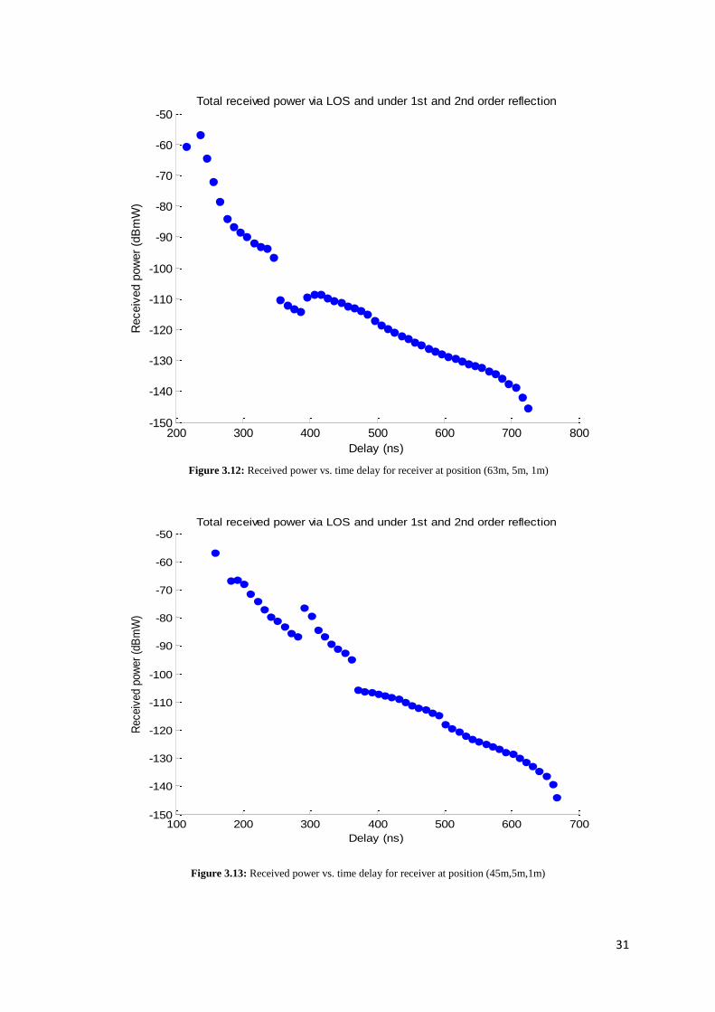
Figure 3.12, 3.13 and 3.14 shows the power distribution vs. time delay considering second order
reflections when the receiver is located at positions (63m, 5m, 1m), (45m, 5m, 1m) and (10m, 5m,
1m) . It is observed that the excess delay becomes very large due to the large signal dispersion. In
addition, because 2nd
order reflected signals travel a long distance to reach the receiver, the
received power is very low. Therefore, they don’t influence strongly received power from single
reflections. The tail of the impulse response appears due the second order reflections from far
reflector which carry only little power.
Figure 3.11: Upper perspective of a room with multiple reflection propagation
31
200 300 400 500 600 700 800-150
-140
-130
-120
-110
-100
-90
-80
-70
-60
-50
Delay (ns)
Receiv
ed p
ow
er
(dB
mW
)
Total received power via LOS and under 1st and 2nd order reflection
Figure 3.12: Received power vs. time delay for receiver at position (63m, 5m, 1m)
100 200 300 400 500 600 700-150
-140
-130
-120
-110
-100
-90
-80
-70
-60
-50
Delay (ns)
Receiv
ed p
ow
er
(dB
mW
)
Total received power via LOS and under 1st and 2nd order reflection
Figure 3.13: Received power vs. time delay for receiver at position (45m,5m,1m)
32
0 100 200 300 400 500 600-140
-130
-120
-110
-100
-90
-80
-70
-60
-50
Delay (ns)
Receiv
ed p
ow
er
(dB
mW
)
Total received power via LOS and under 1st and 2nd order reflection
Figure 3.14: Received power vs. time delay for receiver at position (10m,5m,1m)
3.5 Simulation result of single reflection model with
four radiators
In most cases, more than one source is used in a conferencing hall so that the whole room can be
covered. Therefore, let’s consider configurations with multiple sources. First we assume that the
four radiators are positioned on the same wall as shown in Figure 3.15 (a) and in a second
configuration Figure 3.15(b) they are positioned in the four corners of the room. We only consider
one selected position for the receiver as shown with the red point at (63m, 5m, 1m). The power
distribution vs. time delay is represented in the following graphs for these two configurations

33
(a) (b)
Figure 3.15: Two configurations of four radiators in the room
Figure 3.16 shows the received power vs. the excess delay for the first configuration (a). The first
four points on the graph belong to the LOS received power of the four radiators which arrive with
about the same delay. Following that there is an exponential decay of power due to diffuse
components which arrive at the receiver. A large excess delay is also generated from the signal
dispersion.
Figure 3.17 represents the power distribution for the second configuration and the same receiver
position. The first point is the LOS received power of the transmitter in the vicinity of the receiver
and three other LOS received powers arrive after that. Because of the orientation angle of the
transmitter there is little received power at a delay about 150ns due to the reflection from very
close reflectors to the transmitter. The amount of the power that is arrived at a large delay is
between -70dBm and -100dBm which are coming from far away reflectors. Since there are four
radiators on each corner of the room, it is obvious that the level of received power does not
decrease significantly for larger delay.

34
200 220 240 260 280 300 320 340 360 380-100
-95
-90
-85
-80
-75
-70
-65
-60
-55
-50
Delay (ns)
Receiv
ed p
ow
er
(dB
mW
)Total received power via LOS and under 1st reflection
Figure 3.16: Received power vs. delay for the receiver shown in first conjuration
0 50 100 150 200 250 300 350 400 450 500-250
-200
-150
-100
-50
0
Delay (ns)
Receiv
ed p
ow
er
(dB
mW
)
Total received power via LOS and under 1st reflection
Figure 3.17: Received power vs. delay for the receiver shown in second configuration

35
3.6 Calculation of delay spread and RMS delay
The importance of calculating delay spread and RMS delay has been discussed in detail in chapter
2. The channel delay spread qualifies the multipath channel in the time domain and RMS delay
limits the maximum symbol rate of the system. Therefore, in this section, we are going to find
these two important parameters which affect the choice of applying multicarrier or single carrier
modulation for the system.
The maximum excess delay is measured with respect to the power level of -30dB and -40dB
below the first received signal. When the received signal is less than this threshold, it is not
considered. Furthermore, if there is a LOS path between transmitter and receiver it is considered
as the first arrival component but in a worse case, it is assumed that the LOS is blocked.
Therefore, in the following graphs, the channel delay spread with -30dB and -40dB thresholds and
RMS delay are presented based on the single and multiple reflections model. Also the assumption
of blocked LOS is considered.
Figures 3.18 and 3.19 show the distribution of the delay spread with -30dB and -40dB threshold
respectively, when the receiver is placed in 24 different positions used in the single reflection
model. The horizontal axis represents receiver positions such that the position 24 is when the
detector is too close to the transmitter. These Figures also show that the delay spread of a NLOS
channel is larger than a LOS channel. It is because the difference between first arrival component
and the -30dB and -40dB ones increase in NLOS channel.
In both Figures, as the receiver is close to the transmitter, there is a rise in the delay spread. In the
worst case when the receiver is located at position (10m, 5m, 1m) the maximum delay spread is
350ns. However, there is an exception in graph 3.17 but it can be neglected.
Figure 3.18: 30dB delay spread with LOS and N-LOS in single reflection channel model
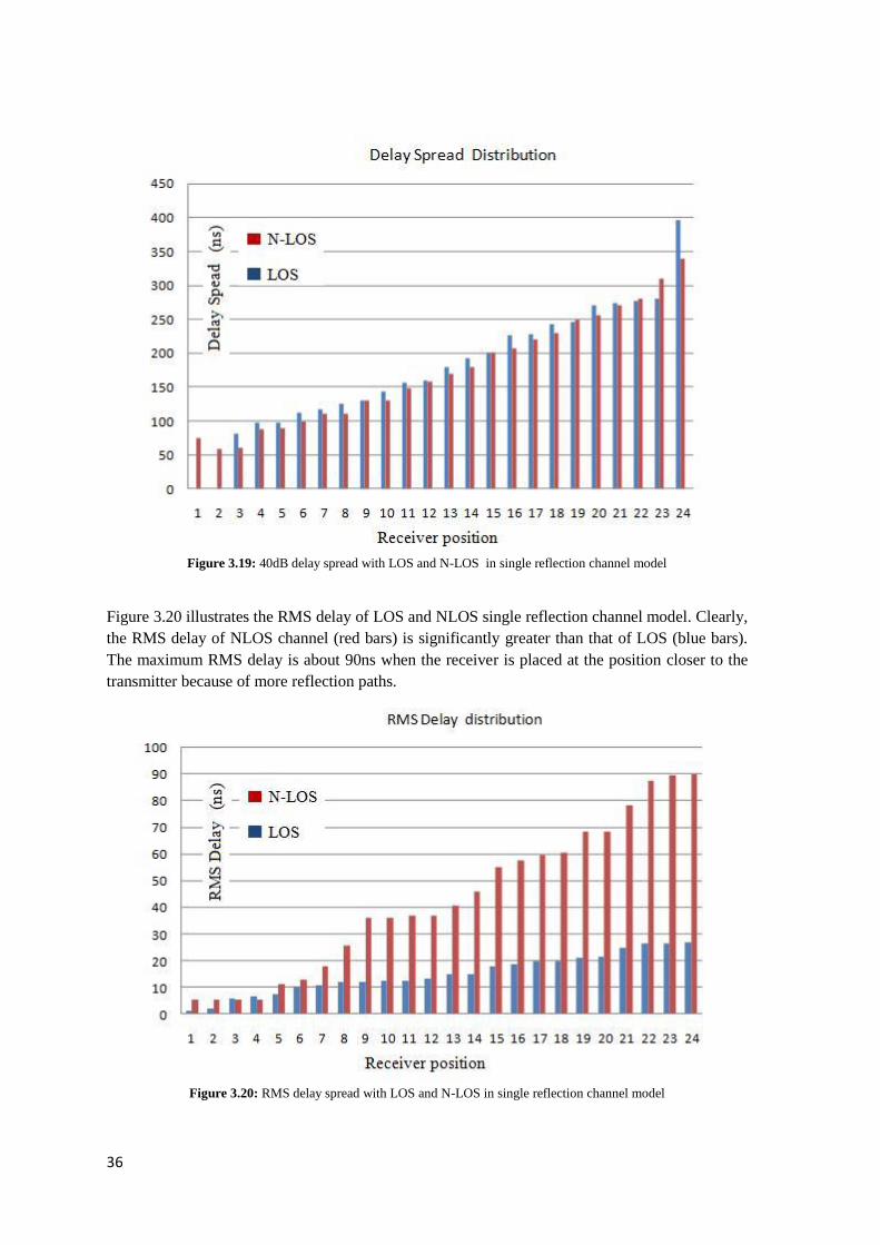
36
Figure 3.19: 40dB delay spread with LOS and N-LOS in single reflection channel model
Figure 3.20 illustrates the RMS delay of LOS and NLOS single reflection channel model. Clearly,
the RMS delay of NLOS channel (red bars) is significantly greater than that of LOS (blue bars).
The maximum RMS delay is about 90ns when the receiver is placed at the position closer to the
transmitter because of more reflection paths.
Figure 3.20: RMS delay spread with LOS and N-LOS in single reflection channel model

37
In Figure 3.21 and 3.22, the delay spread of the multiple reflection channel model are shown for -
30dB and -40B respectively. The same behavior as seen in single reflection model is formed in
the following Figures. It is very interesting to be noted that considering second reflections don’t
influence the maximum delay spread. Maximum delay spread is about 350ns in both Figures.
Figure 3.21: 30dB delay spread with LOS and N-LOS in multi reflections channel model
Figure 3.22: 40dB delay spread with LOS and N-LOS in multi reflections channel model
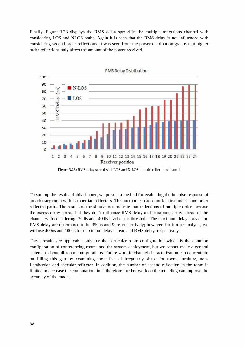
38
Finally, Figure 3.23 displays the RMS delay spread in the multiple reflections channel with
considering LOS and NLOS paths. Again it is seen that the RMS delay is not influenced with
considering second order reflections. It was seen from the power distribution graphs that higher
order reflections only affect the amount of the power received.
Figure 3.23: RMS delay spread with LOS and N-LOS in multi reflections channel
To sum up the results of this chapter, we present a method for evaluating the impulse response of
an arbitrary room with Lambertian reflectors. This method can account for first and second order
reflected paths. The results of the simulations indicate that reflections of multiple order increase
the excess delay spread but they don’t influence RMS delay and maximum delay spread of the
channel with considering -30dB and -40dB level of the threshold. The maximum delay spread and
RMS delay are determined to be 350ns and 90ns respectively; however, for further analysis, we
will use 400ns and 100ns for maximum delay spread and RMS delay, respectively.
These results are applicable only for the particular room configuration which is the common
configuration of conferencing rooms and the system deployment, but we cannot make a general
statement about all room configurations. Future work in channel characterization can concentrate
on filling this gap by examining the effect of irregularly shape for room, furniture, non-
Lambertian and specular reflector. In addition, the number of second reflection in the room is
limited to decrease the computation time, therefore, further work on the modeling can improve the
accuracy of the model.
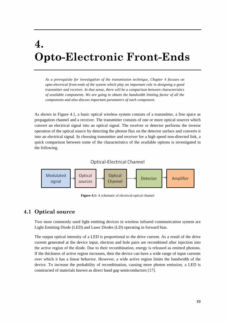
39
4.
Opto-Electronic Front-Ends
As a prerequisite for investigation of the transmission technique, Chapter 4 focuses on
opto-electrical front-ends of the system which play an important role in designing a good
transmitter and receiver. In that sense, there will be a comparison between characteristics
of available components. We are going to obtain the bandwidth limiting factor of all the
components and also discuss important parameters of each component.
As shown in Figure 4.1, a basic optical wireless system consists of a transmitter, a free space as
propagation channel and a receiver. The transmitter consists of one or more optical sources which
convert an electrical signal into an optical signal. The receiver or detector performs the inverse
operation of the optical source by detecting the photon flux on the detector surface and converts it
into an electrical signal. In choosing transmitter and receiver for a high speed non-directed link, a
quick comparison between some of the characteristics of the available options is investigated in
the following.
Figure 4.1: A schematic of electrical-optical channel
4.1 Optical source
Two most commonly used light emitting devices in wireless infrared communication system are
Light Emitting Diode (LED) and Laser Diodes (LD) operating in forward bias.
The output optical intensity of a LED is proportional to the drive current. As a result of the drive
current generated at the device input, electron and hole pairs are recombined after injection into
the active region of the diode. Due to their recombination, energy is released as emitted photons.
If the thickness of active region increases, then the device can have a wide range of input currents
over which it has a linear behavior. However, a wide active region limits the bandwidth of the
device. To increase the probability of recombination, causing more photon emission, a LED is
constructed of materials known as direct band gap semiconductors [17].
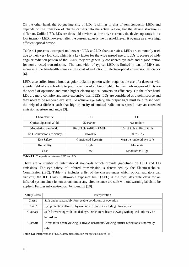
40
On the other hand, the output intensity of LDs is similar to that of semiconductor LEDs and
depends on the transition of charge carriers into the active region, but the device structure is
different. Unlike LED, LDs are threshold devices; at low drive currents, the device operates like a
low intensity LED, however, after the current exceeds the threshold level, it operate as a very high
efficient optical device.
Table 4.1 presents a comparison between LED and LD characteristics. LEDs are commonly used
due to their very low cost which is a key factor for the wide spread use of LEDs. Because of wide
angular radiation pattern of the LEDs, they are generally considered eye-safe and a good option
for non-directed transmission. The bandwidth of typical LEDs is limited in tens of MHz and
increasing the bandwidth comes at the cost of reduction in electro-optical conversion efficiency
[6].
LEDs also suffer from a broad angular radiation pattern which requires the use of a detector with
a wide field of view leading to poor rejection of ambient light. The main advantages of LDs are
the speed of operation and much higher electro-optical conversion efficiency. On the other hand,
LDs are more complex and more expensive than LEDs. LDs are considered as a point source and
they need to be rendered eye safe. To achieve eye safety, the output light must be diffused with
the help of a diffuser such that high intensity of emitted radiation is spread over an extended
emission aperture and angle [3].
Characteristic LED LD
Optical Spectral Width 25-100 nm 0.1 to 5nm
Modulation bandwidth 10s of kHz to100s of MHz 10s of kHz to10s of GHz
E/O Conversion efficiency 10 to20% 30 to 70%
Eye Safety Considered Eye safe Must be rendered eye safe
Reliability High Moderate
Cost Low Moderate to High
Table 4.1: Comparison between LED and LD
There are a number of international standards which provide guidelines on LED and LD
emissions. The eye safety of infrared transmission is determined by the Electro-technical
Commission (IEC). Table 4.2 includes a list of the classes under which optical radiators can
transmit; the IEC Class 1 allowable exposure limit (AEL) is the most desirable class for an
infrared system since its emissions under any circumstance are safe without warning labels to be
applied. Further information can be found in [18].
Safety Class Interpretation
Class1 Safe under reasonably foreseeable conditions of operation
Class2 Eye protection afforded by aversion responses including blink reflex
Class3A Safe for viewing with unaided eye. Direct intra-beam viewing with optical aids may be
hazardous
Class3B Direct intra-beam viewing is always hazardous. viewing diffuse reflections is normally
safe
Table 4.2: Interpretation of LED safety classification for optical sources [18]

41
Because of the mentioned advantages of LEDs and the system required bandwidth in tens of
MHz, the optical sources for the system in this work are chosen to be LEDs.
In general, there are a few characteristics of LEDs that designers have to consider: rise and fall
time, peak wavelength, radiant power P , radiation pattern and ( P I ) current to power
characteristic. The mentioned parameters are discussed briefly in the following and used in the
next step to select an appropriate LED.
LED Bandwidth
The main disadvantage of the LED is its low modulation bandwidth as compared with the laser
diode. Modulation bandwidth is determined by the minority carrier lifetime, life , in the light
emitting active region as
3
1
2dB
life
f Hz
(4.1)
In addition, carrier life time determines the rise and fall times of the LED which is
approximately 2.2rise . Therefore, In order to achieve high speed data transmission, the LED
should have small rise and fall times to make it fast.
Peak Wavelength
Peak wavelength ( p ) refers to the wavelength at which the light source produce its maximum
emission intensity. Manufacturers usually specify the maximum and minimum value for λp and it
is temperature dependent such that the optical spectrum becomes wider with increasing
temperature.
Radiant Power
The total radiated power of the LED is called radiant power or radiant intensity and measured in
watt or watt per steradian (W/sr), respectively. The light detected by a receiver depends on the
radian intensity emitted toward the receiver. Suppose a transmitter emits a radiation pattern
described by the radiant intensity (W/sr) ( )tPR where ( )R is the radiation pattern (Eq.2.5). At
the receiver located at distance r and angle with respect to the transmitter, the irradiance
(W/cm²) is2( , ) ( ) /ir tI d PR r . Then the received power (W) is ( , )r ir RxP I d A where,
RxA is area of the detector.

42
Radiant power - Current (P-I) curve
The radiant output power vs. forward current characteristic shows the linearity of the
LED. The linearity curve of the LED can be found in the data sheet of LED. It represents
the degree to which the optical output is directly proportional to the electrical current input. The
radiant power-current characteristic is temperature dependent, it means for a given input
current, the optical output power falls as temperature increases.
4.2 Infrared receiver
A typical optical wireless receiver consists of an optical lens and optical filter, photo-detector and
preamplifier as shown in Figure 4.2. The optical lens is used to increase the effective area of the
photo-detector and collects radiation. The optical filter is used to reject the out of band ambient
illumination. The photo detector converts optical radiation into a photo-current and the
preamplifier amplify the signal and converts it into voltage. In this section we only focus on the
photo detector and the preamplifier.
Figure 4.2: A typical OW receiver [7]
4.2.1 Photo-detector
The main component of an optical wireless receiver is the photo detector which coverts light into
electrical current. When light reaches a photo detector, the incident photons generate free
electron-hole pairs if they have sufficient energy. The diffusion of these charge carriers in the
detector constitutes the detected photo-current. To collect sufficient energy, a large area photo-
detector must be used. A large photo diode is of the interest but it limits electrical due to high
capacitance.
There are two practical options for a detector: Positive-Intrinsic-Negative Diode (PIN) and
avalanche photodiodes (APD) in Si-technology.
PIN diodes are constructed by placing high-resistivity intrinsic I region between a P-type and N-
type region. When photons arrive at the detector, they are observed in the intrinsic region and
every absorbed photon generates one electron-hole pair in the intrinsic region. Because of the
electric field generated in this region, these carriers are swept up and collected across the junction
which is the origin of the photo-current [17]. The APD is constructed similar to PIN diode and the
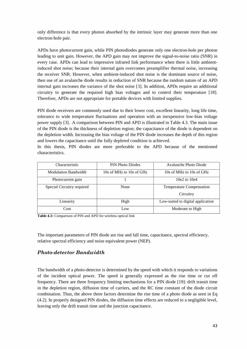
43
only difference is that every photon absorbed by the intrinsic layer may generate more than one
electron-hole pair.
APDs have photocurrent gain, while PIN photodiodes generate only one electron-hole per photon
leading to unit gain. However, the APD gain may not improve the signal-to-noise ratio (SNR) in
every case. APDs can lead to impressive infrared link performance when there is little ambient-
induced shot noise; because their internal gain overcomes preamplifier thermal noise, increasing
the receiver SNR. However, when ambient-induced shot noise is the dominant source of noise,
then use of an avalanche diode results in reduction of SNR because the random nature of an APD
internal gain increases the variance of the shot noise [3]. In addition, APDs require an additional
circuitry to generate the required high bias voltages and to control their temperature [18].
Therefore, APDs are not appropriate for portable devices with limited supplies.
PIN diode receivers are commonly used due to their lower cost, excellent linearity, long life time,
tolerance to wide temperature fluctuations and operation with an inexpensive low-bias voltage
power supply [3]. A comparison between PIN and APD is illustrated in Table 4.3. The main issue
of the PIN diode is the thickness of depletion region; the capacitance of the diode is dependent on
the depletion width. Increasing the bias voltage of the PIN diode increases the depth of this region
and lowers the capacitance until the fully depleted condition is achieved.
In this thesis, PIN diodes are more preferable to the APD because of the mentioned
characteristics.
Characteristic PIN Photo Diodes Avalanche Photo Diode
Modulation Bandwidth 10s of MHz to 10s of GHz 10s of MHz to 10s of GHz
Photocurrent gain 1 10e2 to 10e4
Special Circuitry required None Temperature Compensation
Circuitry
Linearity High Low-suited to digital application
Cost Low Moderate to High
Table 4.3: Comparison of PIN and APD for wireless optical link
The important parameters of PIN diode are rise and fall time, capacitance, spectral efficiency,
relative spectral efficiency and noise equivalent power (NEP).
Photo-detector Bandwidth
The bandwidth of a photo-detector is determined by the speed with which it responds to variations
of the incident optical power. The speed is generally expressed as the rise time or cut off
frequency. There are three frequency limiting mechanisms for a PIN diode [19]: drift transit time
in the depletion region, diffusion time of carriers, and the RC time constant of the diode circuit
combination. Thus, the above three factors determine the rise time of a photo diode as seen in Eq
(4.2). In properly designed PIN diodes, the diffusion time effects are reduced to a negligible level,
leaving only the drift transit time and the junction capacitance.
44
2 2 2
rise drift diff RCt t t t (4.2)
where, 2.2RC t Lt C R and 2/ /drift d Rt d v d V , d is depletion layer width, is the
traveling rate , RV the reverse voltage, tC is the sum of the photodiode junction and input
capacitances on the inverting terminal of the amplifier and LR the load resistance. Consequently,
the rise time roughly relates to the cutoff frequency,cf in the formula:
0.35
c
rise
ft
(4.3)
Spectral efficiency [A/W]
Spectral efficiency is the ratio of the radiant power to the resulting photo current. The higher is
the value of spectral efficiency, the larger is the current generated by the PIN diode. So it is
necessary to have as spectral efficiency as large possible.
Relative spectral efficiency
The PIN diode needs to have maximum relative radiant power at the same wavelength as LED.
Noise equivalent power (NEP)
There are two sources of noise in a high speed PIN diode: shot noise, and electronic Johnson
noise. Shot noise is related to the statistical fluctuation in both photocurrent and dark current. The
magnitude of the shot noise is expressed as
2 ( )sn p DI q I I f (4.4)
where q =1.6x10⁻¹⁹C, is the electron charge, pI is the photo-generated current, DI is the photo-
detector dark current and f is measurement bandwidth. The load resistance of a photo detector
generates the Johnson noise due to the thermal generation of carriers. The magnitude of this
generated current noise is:
4 B m
jn
L
k T fI
R
(4.5)
Where Bk =1.38 x 2310
is the Boltzmann Constant, mT is the absolute temperature in degrees
Kelvin, f is the bandwidth and LR is the load resistance of the photodiode. The total noise current
generated in a photo-detector is determined by:
2 2
tn sn jnI I I (4.6)
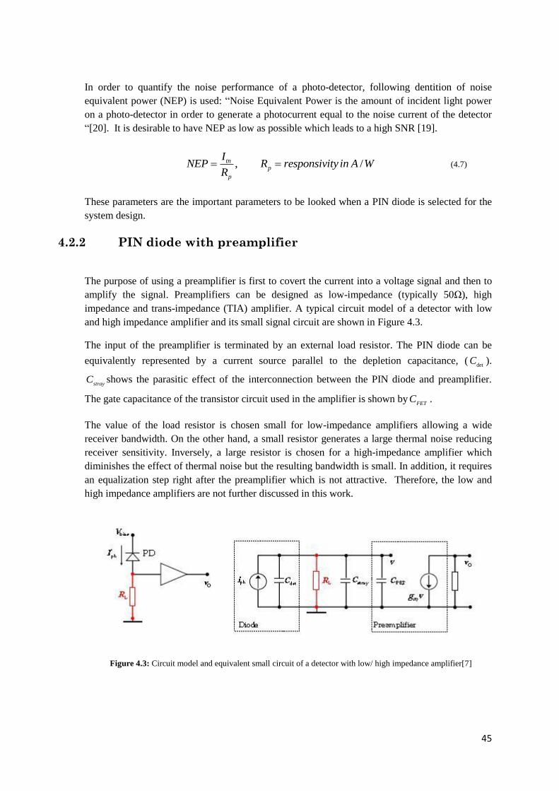
45
In order to quantify the noise performance of a photo-detector, following dentition of noise
equivalent power (NEP) is used: “Noise Equivalent Power is the amount of incident light power
on a photo-detector in order to generate a photocurrent equal to the noise current of the detector
“[20]. It is desirable to have NEP as low as possible which leads to a high SNR [19].
, /tnp
p
INEP R responsivity in A W
R (4.7)
These parameters are the important parameters to be looked when a PIN diode is selected for the
system design.
4.2.2 PIN diode with preamplifier
The purpose of using a preamplifier is first to covert the current into a voltage signal and then to
amplify the signal. Preamplifiers can be designed as low-impedance (typically 50Ω), high
impedance and trans-impedance (TIA) amplifier. A typical circuit model of a detector with low
and high impedance amplifier and its small signal circuit are shown in Figure 4.3.
The input of the preamplifier is terminated by an external load resistor. The PIN diode can be
equivalently represented by a current source parallel to the depletion capacitance, (det
C ).
strayC shows the parasitic effect of the interconnection between the PIN diode and preamplifier.
The gate capacitance of the transistor circuit used in the amplifier is shown byFET
C .
The value of the load resistor is chosen small for low-impedance amplifiers allowing a wide
receiver bandwidth. On the other hand, a small resistor generates a large thermal noise reducing
receiver sensitivity. Inversely, a large resistor is chosen for a high-impedance amplifier which
diminishes the effect of thermal noise but the resulting bandwidth is small. In addition, it requires
an equalization step right after the preamplifier which is not attractive. Therefore, the low and
high impedance amplifiers are not further discussed in this work.
Figure 4.3: Circuit model and equivalent small circuit of a detector with low/ high impedance amplifier[7]
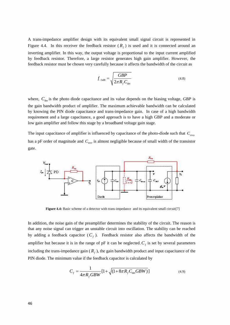
46
A trans-impedance amplifier design with its equivalent small signal circuit is represented in
Figure 4.4. In this receiver the feedback resistor (fR ) is used and it is connected around an
inverting amplifier. In this way, the output voltage is proportional to the input current amplified
by feedback resistor. Therefore, a large resistor generates high gain amplifier. However, the
feedback resistor must be chosen very carefully because it affects the bandwidth of the circuit as
3
det2dB
f
GBPf
R C (4.8)
where, detC is the photo diode capacitance and its value depends on the biasing voltage, GBP is
the gain bandwidth product of amplifier. The maximum achievable bandwidth can be calculated
by knowing the PIN diode capacitance and trans-impedance gain. In case of a high bandwidth
requirement and a large capacitance, a good approach is to have a high GBP and a moderate or
low gain amplifier and follow this stage by a broadband voltage gain stage.
The input capacitance of amplifier is influenced by capacitance of the photo-diode such that stray
C
has a pF order of magnitude and FET
C is almost negligible because of small width of the transistor
gate.
Figure 4.4: Basic scheme of a detector with trans-impedance and its equivalent small circuit[7]
In addition, the noise gain of the preamplifier determines the stability of the circuit. The reason is
that any noise signal can trigger an unstable circuit into oscillation. The stability can be reached
by adding a feedback capacitor ( fC ). Feedback resistor also affects the bandwidth of the
amplifier but because it is in the range of pF it can be neglected. fC is set by several parameters
including the trans-impedance gain ( fR ), the gain bandwidth product and input capacitance of the
PIN diode. The minimum value if the feedback capacitor is calculated by
det
1[1 (1 8 )]
4f f
f
C R C GBWR GBW
(4.9)

47
In the following, a few characteristics of the trans-impedance amplifier are introduced; input
current noise, input current voltage, input equivalent noise.
Input current and voltage noise
The noise of an amplifier can be completely specified in terms of two noise sources, input current
noise ni
and input voltage noise ne as shown in Figure 4.5.
ni is the noise that occurs at the input
of the noiseless amplifier due to fluctuations in the current and it is expressed in ( /pA Hz ). ne is
the voltage noise seen at the input of the noiseless amplifier if the input terminal is shorted and it
is expressed in ( /nV Hz ).These values are provided in the amplifier data sheets.
Figure 4.5: Noise characteristic of a amplifier [21]
Input equivalent noise
Input equivalent noise is the relationship in which all noise sources are added at the input of the
amplifier in RMS fashion; that is, as the square root of the sum of the squares and generates the
equivalent current noise if the total output noise is band limited to a frequency less than the
feedback pole frequency. The feedback pole frequency is defined by 1/ 2 F Ff R C to provide
stability of the amplifier. A very simple expression for the equivalent input noise current can be
derived as [22]
2 2 2det24
( ) ( )3
n NEQ n
F F
e e C FkTI i
R R
(4.10)
where:
EQI = Equivalent input noise current if the output noise is band limited to 1/ 2 F Ff R C
ni = Input current noise for the op amp inverting input
ne = Input voltage noise for the op amp
detC = Diode capacitance
F = Band limiting frequency in Hz (usually a post filter prior to further signal processing)
If phase modulation techniques are used to transmit information, another important parameter is
the phase characteristic of the signal.

48
This chapter has looked at various important parameters of LED, PIN diode and preamplifier. We
presented a detailed noise and bandwidth analysis for a PIN diode and a preamplifier. The results
indicate that to achieve large bandwidth, a detector with small capacitance and large area is
required. Hence, the area of the detector can be calculated if for example the bandwidth of
20MHz is required. As mentioned in chapter 2, for an infrared system, the noise is generated from
internal component as well, which the noise of two main components in the receiver front-end
was discussed here.
With respect to the current system design, input equivalent noise is the dominate source of the
noise which is used to determine SNR. As future work, the noise power of the receiver front-end
can be easily determined for a specific design.

49
5.
Experimental investigation
to increase the bandwidth
In this chapter, first we will show the new available opto-electrical components in the
market and discuss their characteristics. The suitable LED, PIN diode and trans-
impedance amplifier will be chosen. Finally, a measurement set up is defined with the
selected components to verify the possibility of increasing the bandwidth of the system.
In chapter 4, we discussed the main characteristics of the opto-electrical components. The optical
source and detector for the system were considered to be a LED and a PIN diode. In this chapter,
we are going to explore whether there are new components available which support a large
bandwidth compared to the components used in the current system.
5.1 Light Emitting Diode
After intensive research through the different manufactures such as Vishay and Osram, several
new light emitting diodes are chosen. Table 5.1 summarizes the primary specifications of these
LEDs. Common IR LEDs are low power emitters, designed for operation at 100mA forward
current and 1.5V forward voltage. Most IR LEDs are intended for tight half beam angle between
10° and 40° and have a cut off frequency between 18 and 35MHz.
Part Number Peak wavelength (nm)
Radiant intensity(mW/sr)
Angle of half intensity
Rise time
Cut off frequency
TSFF5400 870 60 22° 10ns 35MHz
TSFF5200 160 10°
VSMF4710 10 60° 15ns 24MHz
TSFF5410 70 22°
TSFF6210 180 10°
TSFF5510 32 38°
TSHG6210 850 230 10° 20ns 18MHz
TSHG6410 90 18°
TSHG6400 70 22°
TSHG6200 160 10° 20MHz
TSHG5510 830 32 38° 15ns 24MHz
TSHG8400 70 22° 20ns 18MHz
TSHG8200 180 10°
SFH 4595 880 60 14° 10ns 35MHz
SFH 4500 950 80 10° 10ns 35MHz
Table 5.1: Light emitting diodes

50
The LED of the current system is TSHF5410 with modulation bandwidth of 12MHz, 22° half
angle, 30ns rise and fall time, 890nm peak wavelength and radiant intensity of 70mW/sr. As
mentioned in 4.1, the rise time is inversely proportional to frequency bandwidth of LED. This
LED is quite slow compared to the new components. Hence, even LED is a bandwidth limiting
factor in the current system design. However, new LEDs support a larger bandwidth compared to
the bandwidth of new PIN diodes, therefore, they are not considered as a bandwidth limiting
components.
As seen in the Table 5.1, LEDs are categorized in terms of peak wavelengths and in the following
the characteristics of some categories are discussed.
Figure 5.1 shows the radiant intensity of the LEDs vs. the angle of half intensity for LEDs with
peak wavelength of 870nm. The red bars represent radiant density of LEDs with rise time of 10ns
relatively 35 MHz bandwidth and green bars are LEDs with 15ns rise time relatively 24MHz
bandwidth.
Figure 5.1: Radiant intensity of the LEDs vs. angle of half intensity, λ=870nm
The chart indicates that radiant intensity significantly decays as the angle of half intensity
becomes larger due to wide beam pattern. Although a LED with an angle of 10° has high a radiant
intensity, it has a very narrow beam pattern. Therefore, the radiation pattern is not wide enough to
cover a large area unless these LEDs are mounted in different direction. The effects of the larger
bandwidth results in slightly decrease in radiant intensity of the LEDs.
Figure 5.2 also shows the relationship between radiant intensity and angle of half intensity for
LED with peak wavelength of 850nm for which the same trend is visible. LEDs listed in Table
5.1 are all faster than the LED used in the current system and applying any of these components
result in an increase in the bandwidth of the transmitter.

51
Figure 5.2: Radiant intensity of the LED vs. angle of half intensity, λ=850nm
As mentioned, light emitting diodes are not considered as a bandwidth limiting factor for the
required bandwidth below 35MHz. TSFF5400 which has the highest bandwidth is not produced
anymore by Vishay. Therefore, the next good option in order to support large bandwidth is
TSFF5410 which has reasonable output intensity and half angle compared to the others. It can
support the frequency bandwidth of 24MHz.
TSHG6400 is also a good option with bandwidth of 18MHz. Final selection of the appropriate
LED has to be made after choosing the PIN diodes because if there does not exist a PIN-diode
supporting 24MHz bandwidth then using a LED with 24 MHz bandwidth only results in intensity
reduction.
5.2 PIN-diode
To select an appropriate PIN photodiode, the important factors of several PIN diodes are listed in
Table 5.2. These parameters were discussed in detail in chapter 4. As seen from Table 5.2, the
junction capacitance is proportional to the area of the PIN diode. Increasing the bias voltage of the
photodiode reduces the junction capacitance and increases the bandwidth.
PIN photodiode used for the current system is SHF235 FA with a rise time of 20ns resulting in
bandwidth of 17.5MHz, which is a common rise time of many PIN diodes. One high speed PIN
diode alternative is TESP5700 which has a 10ns rise time supporting a 35MHz bandwidth and
includes day light filter. However, the fast rise time is achieved at the expense of small area and
low output current. In addition, it was also mentioned in chapter 4 that the small area of the PIN
diode can be compensated by using several PIN diodes or a hemispherical lens with the gain2
dn ,
2
dn is lens index. The peak wavelength for this diode is equal to the infrared emitter TSFF5410
chosen for high speed communication. Whether there is a lens to provide enough gain needs to be
checked.

52
Part Number
Spectral efficiency
Rise time
Peak Wavelength (nm)
Capacitance (pF)
NEP Area (mm2)
angle output
BP 104 F,FS 0.70 20ns
950 48
3.6e-14 4.48 60
35μA
BF 104 FAS 0.65 880 34μA
BF 104 S,BS104 SR
0.62 850 55μA
BPW 34 F 0.59 950 72 4.3e-14 7 80μA
SFH2400,FA - 5 850 11 2.9e-14 1 10μA
SFH 2701 0.5 1.2 820 5 6.3e-15 0.36 1.2μA
BPW 34,FS,FSR
0.59 25 950 72 4.3e-14 7 50μA
SFH 225 FA 0.63 20 900 48 3.6e-14 4.48 60 34μA
SFH 235 FA 0.63 20 900 72 4e-14 7 65 50μA
TESP5700 0.57 10 870 17 - 2.2 60 25 µA
BPV10 0.55 2.5 920 11 3e-14 0.78 20
70 µA
BPV10NF 0.55 2.5 940 11 60µA
BPW 34 FA, FAS,R18R
0.65 20 880 72 3.9e-14 7 60 50μA
S6968-01 0.55 - 850 50 6.3e-15 150 35 1.2μA Table 5.2: PIN diodes
5.3 Trans-impedance amplifier (TIA)
A typical trans-impedance amplifier circuit with all necessary components was shown previously
in Figure 4.4. Figure 5.3 shows an example of achievable bandwidth versus trans-impedance gain
for a 10pF source capacitance for various amplifiers.
The OPA847 has a 3.9GHz GBP with 0.85nV/√Hz input voltage noise. The OPA846 has a
1.75GHz GBP with a 1.2nV/√Hz input voltage noise. The OPA843 is an 800MHz GBP device
with a 2nV/√Hz input voltage noise. Finally, the OPA657 is a 1.65GHz GBP device with a
4.8nV/√Hz input voltage noise. Unlike the other three devices, the OPA657 is a FET input
amplifier.
Looking at achievable bandwidth, OP847 provides the highest supporting bandwidth for different
trans-impedance gains. Looking at the noise, OP847 yields a 2.5pA/√Hz input noise current and
0.85nV/√Hz input noise voltage. This amplifier has a much lower voltage noise and higher noise
current. Low input voltage noise is required for best sensitivity in wideband trans-impedance
application [23].
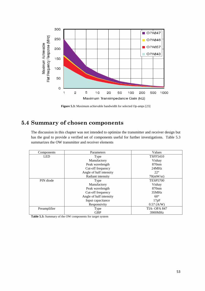
53
Figure 5.3: Maximum achievable bandwidth for selected Op-amps [23]
5.4 Summary of chosen components
The discussion in this chapter was not intended to optimize the transmitter and receiver design but
has the goal to provide a verified set of components useful for further investigations. Table 5.3
summarizes the OW transmitter and receiver elements
Components Parameters Values
LED Type
Manufactory
Peak wavelength
Cut-off frequency
Angle of half intensity
Radiant intensity
TSFF5410
Vishay
870nm
24MHz
22°
70(mW/sr)
PIN diode Type
Manufactory
Peak wavelength
Cut-off frequency
Angle of half intensity
Input capacitance
Responsivity
TESP5700
Vishay
870nm
35MHz
60°
17pF
0.57 (A/W)
Preamplifier Type
GBP
TIA- OPA 847
3900MHz Table 5.3: Summary of the OW components for target system
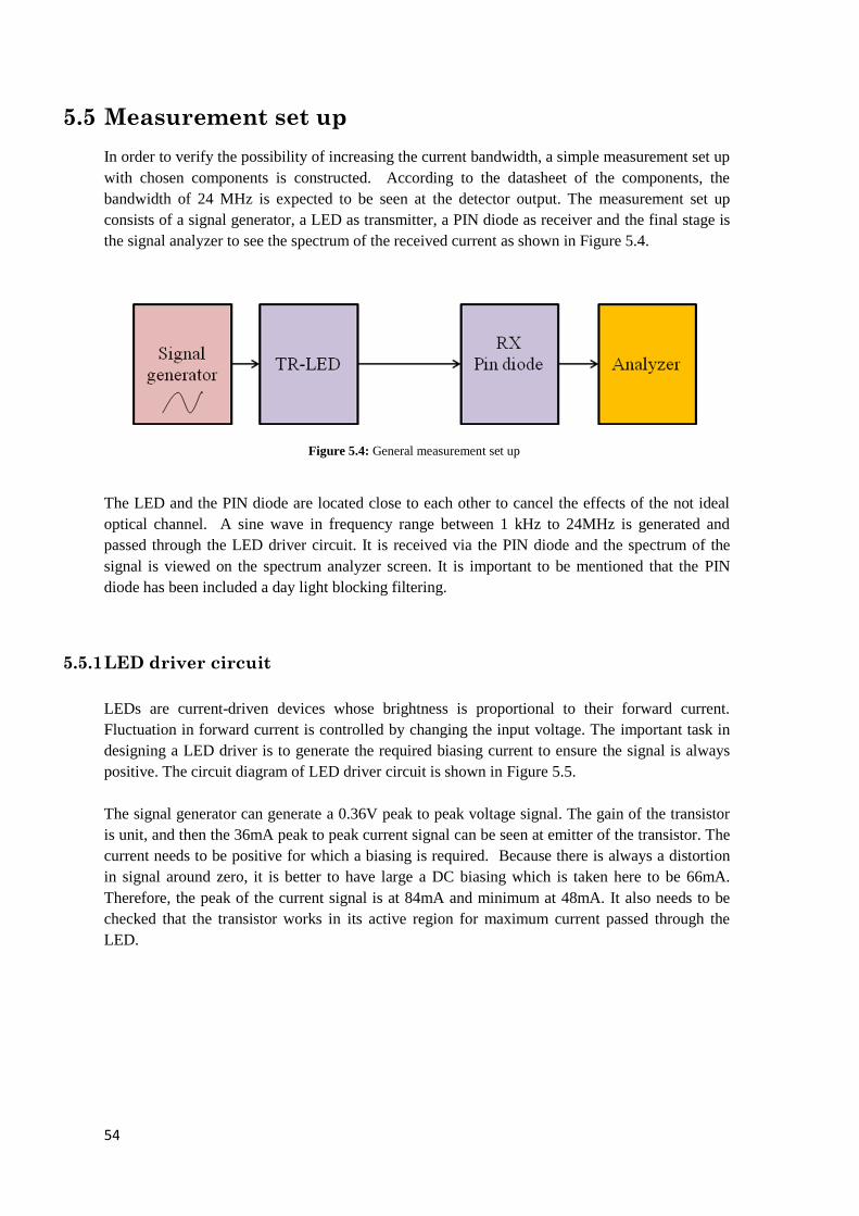
54
5.5 Measurement set up
In order to verify the possibility of increasing the current bandwidth, a simple measurement set up
with chosen components is constructed. According to the datasheet of the components, the
bandwidth of 24 MHz is expected to be seen at the detector output. The measurement set up
consists of a signal generator, a LED as transmitter, a PIN diode as receiver and the final stage is
the signal analyzer to see the spectrum of the received current as shown in Figure 5.4.
Figure 5.4: General measurement set up
The LED and the PIN diode are located close to each other to cancel the effects of the not ideal
optical channel. A sine wave in frequency range between 1 kHz to 24MHz is generated and
passed through the LED driver circuit. It is received via the PIN diode and the spectrum of the
signal is viewed on the spectrum analyzer screen. It is important to be mentioned that the PIN
diode has been included a day light blocking filtering.
5.5.1 LED driver circuit
LEDs are current-driven devices whose brightness is proportional to their forward current.
Fluctuation in forward current is controlled by changing the input voltage. The important task in
designing a LED driver is to generate the required biasing current to ensure the signal is always
positive. The circuit diagram of LED driver circuit is shown in Figure 5.5.
The signal generator can generate a 0.36V peak to peak voltage signal. The gain of the transistor
is unit, and then the 36mA peak to peak current signal can be seen at emitter of the transistor. The
current needs to be positive for which a biasing is required. Because there is always a distortion
in signal around zero, it is better to have large a DC biasing which is taken here to be 66mA.
Therefore, the peak of the current signal is at 84mA and minimum at 48mA. It also needs to be
checked that the transistor works in its active region for maximum current passed through the
LED.
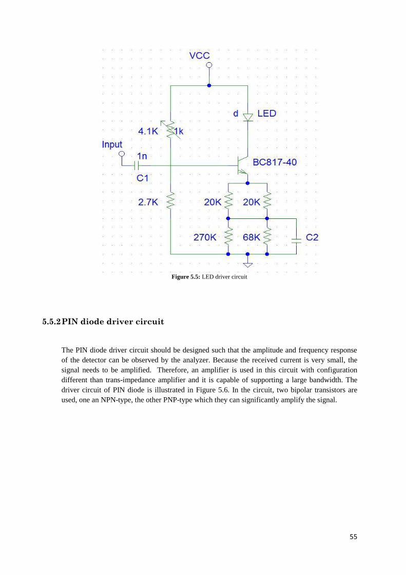
55
Figure 5.5: LED driver circuit
5.5.2 PIN diode driver circuit
The PIN diode driver circuit should be designed such that the amplitude and frequency response
of the detector can be observed by the analyzer. Because the received current is very small, the
signal needs to be amplified. Therefore, an amplifier is used in this circuit with configuration
different than trans-impedance amplifier and it is capable of supporting a large bandwidth. The
driver circuit of PIN diode is illustrated in Figure 5.6. In the circuit, two bipolar transistors are
used, one an NPN-type, the other PNP-type which they can significantly amplify the signal.
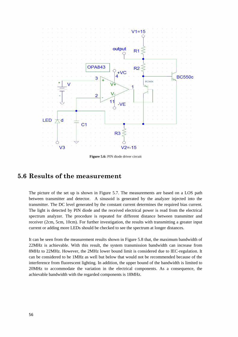
56
Figure 5.6: PIN diode driver circuit
5.6 Results of the measurement
The picture of the set up is shown in Figure 5.7. The measurements are based on a LOS path
between transmitter and detector. A sinusoid is generated by the analyzer injected into the
transmitter. The DC level generated by the constant current determines the required bias current.
The light is detected by PIN diode and the received electrical power is read from the electrical
spectrum analyzer. The procedure is repeated for different distance between transmitter and
receiver (2cm, 5cm, 10cm). For further investigation, the results with transmitting a greater input
current or adding more LEDs should be checked to see the spectrum at longer distances.
It can be seen from the measurement results shown in Figure 5.8 that, the maximum bandwidth of
22MHz is achievable. With this result, the system transmission bandwidth can increase from
8MHz to 22MHz. However, the 2MHz lower bound limit is considered due to IEC-regulation. It
can be considered to be 1MHz as well but below that would not be recommended because of the
interference from fluorescent lighting. In addition, the upper bound of the bandwidth is limited to
20MHz to accommodate the variation in the electrical components. As a consequence, the
achievable bandwidth with the regarded components is 18MHz.

57
Figure 5.7: Measurement set up
Figure 5.8: Spectrum of the received signal

59
6.
Digital Modulation
Techniques
In this chapter, various modulation schemes will be introduced. Then it
will focus on the comparison of these modulations in terms of bandwidth
and power efficiency. It is followed by discussing the bit error rate and
peak to average power ratio for different modulations.
6.1 Modulation scheme classification
There exist a multitude of modulation techniques which are generated by combining and varying
of basic modulations, amplitude shift keying (ASK), frequency shift keying (FSK) and phase shift
keying (PSK). In general, the modulation schemes can be classified into two groups based on
their sensitivity to non-linear distortion: 1. constant envelope modulation and, 2. variable
envelope modulation schemes as shown in Figure 6.1.
Figure 6.1: Modulation scheme classification
60
6.1.1 Constant envelop modulation (CE)
Constant envelope modulation is categorized into two groups: continuous phase modulation
(CPM) and frequency shift key (FSK). CPM includes minimum shift key (MSK), sinusoidal
frequency shift key (SFSK) and Gaussian minimum shift key (GMSK). Thus, the information
bits are encoded either in the frequency or continuous phase. In this sense, signals suffer less
distortion in high power amplifiers. It means that the amplifier device can operate in a nonlinear
mode or near saturation. However, they don’t permit high bandwidth efficiency as compared with
variable envelope modulation. Because the modulation schemes are non-linear it requires higher
bandwidth occupancy than amplitude and phase modulation techniques [9]. Consequently,
because the bandwidth limitation is the primary concern of this project, FSK and CPM schemes
are not considered in this work.
6.1.2 Variable Envelop Modulation
Variable envelope modulation has better spectral properties than constant envelope. However,
because the information bits are encoded in both amplitude and phase of the transmitted signal,
they are more susceptible to variation from fading and interference. In addition, they also require
linear amplifiers which are expensive and less power efficient than non-linear amplifier.
Therefore, the trade off between variable and constant envelope is for better spectral efficiency,
better power efficiency and resistance to channel impairment.
For variable envelope modulation, the size of the constellation must be chosen. The larger the
constellation, the higher data rate is achievable for a given signal bandwidth, but, the signal is
more susceptible to noise fading and the system is hard to implement.
Generally, variable envelop modulation is categorized into the two groups: phase shift keying
(PSK) and amplitude shift keying (ASK). PSK is not classified as a constant envelope because of
its discontinuous phase shift. Amplitude and phase shift keying (MAPSK) is another type of PSK.
Quadrature amplitude modulation is combination of ASK and PSK and it has different
constellation shape, square QAM, star QAM, hexagonal QAM, rounded QAM, staggered QAM
(SQAM).
6.1.2.1 Phase shift keying (MPSK)
In multi level phase shift key (MPSK), the phase of the carrier is shifted to one of the M possible
values 2 ( 1) /i M where 1i M . The constellation points are positioned on a circle
which it provides the highest immunity to corruption and maximum separation in phase between
adjacent points. Another advantage of this is that the symbols are transmitted with the same
energy. In practice, 8PSK is usually the highest order of PSK and more than 8 phases result in
power penalty [9].

61
6.1.2.2 Amplitude Phase shift keying (MAPSK)
MAPSK methods generate transmitted signal by varying both amplitude and phase of the carrier
signal. The constellation of MAPSK is made up of concentric PSK rings as shown in Figure 6.2.
It is widely used in satellite communication including European digital video broadcasting where
high transfer efficiency is essential. MAPSK has various signal constellations which 16 APSK
shows a good performance in case of nonlinear characteristics of an amplifier [23]. One
advantage of 16APSK is to have two concentric-rings with only two amplitude levels. This gives
a reduction in amplitude levels and decrease peak to average power radio (PAPR) when the
16APSK is used in Orthogonal Frequency Division Multiplexing (OFDM) systems
[24].Practically, for 16APSK the symbol energy has to be kept large enough to compensate for
the close distance between the adjacent points in the constellation. Otherwise symbols are highly
sensitive to noise.
Figure 6.2: 16APSK constellation diagram
6.1.2.3 Quadrature Amplitude Modulation (M-QAM)
In quadrature amplitude modulation (M-QAM), the information bits are encoded in both
amplitude and phase of the transmitted signal. Common square constellations are 4-QAM and 16-
QAM. In case of 16-QAM, 4 bits are transmitted per symbol and they are mapped onto the In-
phase and quadrature symbols. Therefore, each constellation point would represent four bits with
two bits on the (I) axis and two bits on the (Q) axis. QAM is more bandwidth efficient than QPSK
but it is vulnerable to non-linear distortion and channel fading effects because distance between
the symbols points on the constellation diagram decreases and to achieve same performance as
QPSK more transmitted power is required.
62
6.2 Comparison of digital modulation schemes
The choice of modulation technique is influenced by several factors such as high spectral
efficiency, high power efficiency, robustness to channel impairment and low implementation cost.
Hence, a desirable modulation provides low bit error rates at low received signal-to-noise ratios
(SNR), performs well in multipath and fading conditions, occupies a minimum bandwidth, and is
cost effective to implement [9]. These requirements are often conflicting and a modulation
scheme does not simultaneously satisfy all of them. The choice of modulation is a trade off
between these requirements and the demand of a particular application. These factors are
discussed in the following for several modulation schemes.
6.2.1 Bandwidth and power efficiency
The Shannon theory states there is upper bound on achievable bandwidth efficiency over a noisy
communication channel and is given by
2
0
log (1 )rb
PR B
N B (bits/sec) (6.1)
where bR is data rate, rP is received signal power, 0N is noise power spectral density (PSD) and
B is bandwidth (Hz). From (6.1), the designers attempt to optimize a system to have a maximum
capacity, however, it can easily be concluded that maximum capacity of the system depends on
the received signal to noise ratio. Therefore, capacity can reach its maximum if input power is
chosen optimally.
As mentioned, designing a digital communication system is a tradeoff between bandwidth and
power efficiency. In many systems, one of them is more valuable than the other. Therefore,
researchers classify systems as either bandwidth or power limited. In case of bandwidth limited
system, spectrally efficient modulation techniques can be used to save bandwidth at the expense
of power. In power limited system, power efferent modulation is used to save power at the
expense of bandwidth. In addition, error correction coding is applied to save the power [25].
Bandwidth efficiency reflects how efficiently a limited bandwidth is utilized and is defined as the
ratio of the data rate per Hertz in a given bandwidth
1/ /
[ ]2 / 2 2
b b b
b s
R T R l bit s
B lT R Hz (6.2)
where l is number of bits per symbol.
Higher level modulation schemes except FSK have high bandwidth efficiency. On the other hand,
they suffer from poor power efficiency. Power efficiency describes the ability of a modulation
technique to protect the reliability of the digital message at low power levels. It is expressed as the
ratio of the signal energy per bit to noise power spectral density (Eb/N0) required at the receiver to

63
achieve a certain probability of error. According to Shannon’s theorem the relation between
bandwidth and power efficiency is given by
2
0
log (1 )b b bR E R
B N B (6.3)
/
0
2 1
/
bR B
b
b
E
N R B
(6.4)
Figure 6.3 represents bandwidth efficiency vs. power efficiency for different modulation schemes
for a given bit error rate of 510. The best modulation scheme is the one closest to the left- hand
corner. As it is observed, QPSK requires 0/ 10bE N dB achieving bandwidth efficiency 2
(bit/s/Hz). 16QAM allows 4 (bit/s/Hz) of transmission bandwidth at 0/ 14bE N dB . This
is because the spacing between the points in the signal constellation decreases. In order to
achieve the same bit error rate more energy per bit is required.
Figure 6.3: Bandwidth efficiency vs. power efficiency [26]
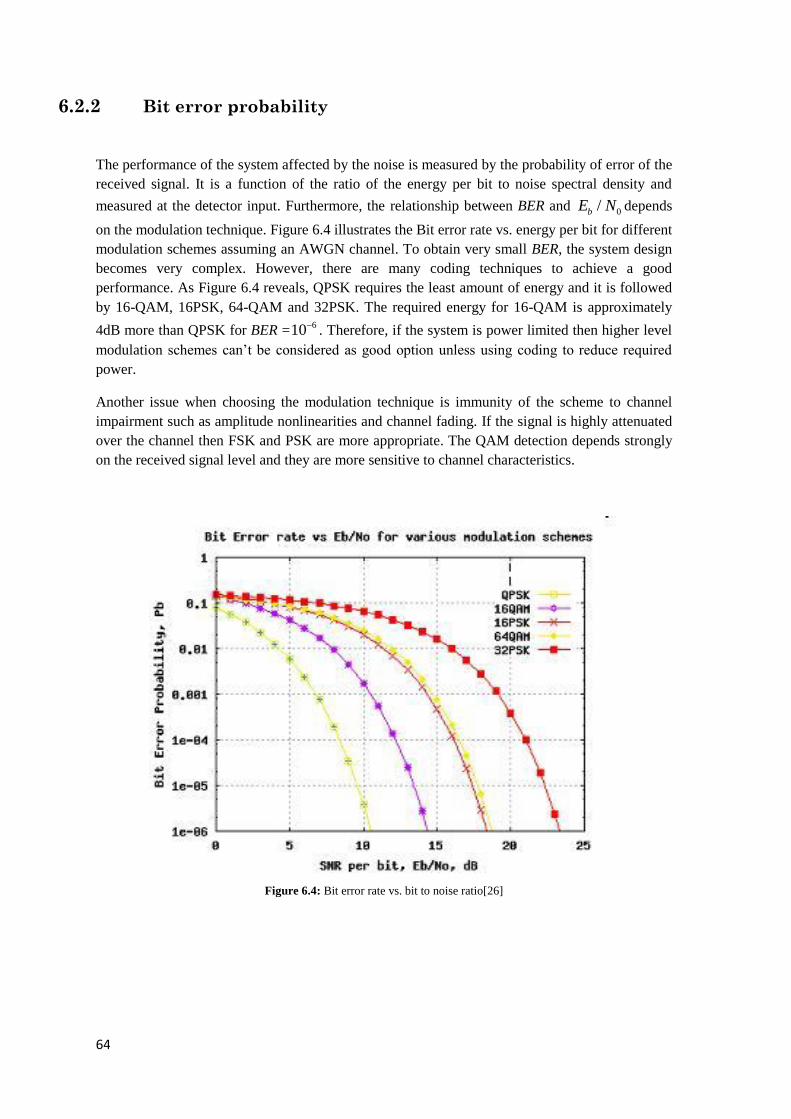
64
6.2.2 Bit error probability
The performance of the system affected by the noise is measured by the probability of error of the
received signal. It is a function of the ratio of the energy per bit to noise spectral density and
measured at the detector input. Furthermore, the relationship between BER and 0/bE N depends
on the modulation technique. Figure 6.4 illustrates the Bit error rate vs. energy per bit for different
modulation schemes assuming an AWGN channel. To obtain very small BER, the system design
becomes very complex. However, there are many coding techniques to achieve a good
performance. As Figure 6.4 reveals, QPSK requires the least amount of energy and it is followed
by 16-QAM, 16PSK, 64-QAM and 32PSK. The required energy for 16-QAM is approximately
4dB more than QPSK for BER =610. Therefore, if the system is power limited then higher level
modulation schemes can’t be considered as good option unless using coding to reduce required
power.
Another issue when choosing the modulation technique is immunity of the scheme to channel
impairment such as amplitude nonlinearities and channel fading. If the signal is highly attenuated
over the channel then FSK and PSK are more appropriate. The QAM detection depends strongly
on the received signal level and they are more sensitive to channel characteristics.
Figure 6.4: Bit error rate vs. bit to noise ratio[26]

65
6.2.3 Peak to average power ratio
The sensitivity of the modulation scheme to non-linear distortion depends on peak to average
power radio (PAPR), which is defined as a ratio of the peak power of the modulated signal to the
average power of the modulated signal. When PAPR is 0 dB there is no variation in amplitude of
the modulated signal. Therefore, the signal is constant envelope and insensitive to nonlinear
distortions. In contrast, amplitude signals (QAM) are subject to non-linear power amplification
with PAPR higher than 0dB.
PAPR values for different modulation schemes with Nyquist filter and with roll cosine factor Nr =
1 are shown in Table 6.1. The PAPR depends on factor of raised cosine filter for a single carrier.
Furthermore, higher level QAM schemes have higher PAPR.
Characteristic Un-filter Nyquist filter( Nr =1)
QPSK 0.00 dB 1.80 dB
8-PSK 0.00 dB 1.80 dB
16-QAM 2.55dB 4.35 dB
64-QAM 3.68 dB 5.50 dB
Table 6.1: Peak to average power ratio (PAPR) of several modulation schemes
67
7.
Multicarrier modulation-
OFDM
This chapter discusses single and multicarrier transmission. It is followed by
describing the concept of an OFDM system as a promising approach to handle
channel dynamics and signal degradation. Finally, challenges in the design an
OFDM system are discussed.
7.1 Multicarrier
The delay of the channel causes a stretching of the input signal which creates signal distortion
referred to as ISI. One way to reduce ISI is to use adaptive filters for equalization. However, to
some extent, it can be complicated due to the filter taps which often increase with number of
reflected channel paths.
ISI can also be significantly reduced by the employment of multicarrier modulation (MCM)
technique. The basic idea of multicarrier modulation is to divide the total bandwidth into many
narrow sub-channels and transmit several bit streams in parallel. Importantly, the number of sub
streams is selected to insure each sub-channel has a bandwidth smaller than the coherent
bandwidth of the channel. Then for a sufficiently large number of sub-channels ( scN ), it can be
assumed that each narrow band sub-channel experiences flat fading.
Figure 7.1 shows how the frequency selective channel affects the signal with a bandwidth B . In
single carrier system, each data symbol occupies the total available bandwidth. Therefore, at the
output of the channel |H (f)|, different parts of the transmitted signal spectrum are attenuated
differently and reconstruction of the signal requires a complex equalization. Consequently, a
narrow band interference or strong frequency band attenuation can cause single carrier
transmission to completely fail.
Multicarrier modulation makes the equalization at the receiver very simple and efficient. In such
system, a data symbol only occupies a fraction of the available bandwidth and different symbols
are transmitted by different sub-bands in parallel. Thus, each sub-channel experiences less ISI and
then the equalization of the signal in each sub-band requires a filter with only one tap. That is the
reason equalization becomes simple [27], [7].

68
Figure 7.1: Passing of baseband and MCM signal through a frequency selective channel [7]
MCM can be implemented using several techniques. The first multicarrier system was introduced
as Frequency Division Multiplexing (FDM). In FDM, the composite multicarrier signal is
obtained by shifting baseband parallel data streams upwards in frequency by modulating them on
different sinusoidal carriers.
The subcarriers of a FDM system must not have overlapping spectra to prevent the channels from
crosstalk that would occur between different sub-channels. To generate non overlapping
subcarriers, frequency guard bands are commonly inserted between subcarriers as shown in
Figure 7.2. The benefit of a guard interval comes at the cost of reducing spectral efficiency.
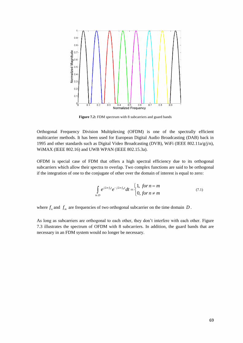
69
Figure 7.2: FDM spectrum with 8 subcarriers and guard bands
Orthogonal Frequency Division Multiplexing (OFDM) is one of the spectrally efficient
multicarrier methods. It has been used for European Digital Audio Broadcasting (DAB) back in
1995 and other standards such as Digital Video Broadcasting (DVB), WiFi (IEEE 802.11a/g/j/n),
WiMAX (IEEE 802.16) and UWB WPAN (IEEE 802.15.3a).
OFDM is special case of FDM that offers a high spectral efficiency due to its orthogonal
subcarriers which allow their spectra to overlap. Two complex functions are said to be orthogonal
if the integration of one to the conjugate of other over the domain of interest is equal to zero:
2 2
1,
0,n mj f t j f t
t D
for n me e dt
for n m
(7.1)
where nf and mf are frequencies of two orthogonal subcarrier on the time domain D .
As long as subcarriers are orthogonal to each other, they don’t interfere with each other. Figure
7.3 illustrates the spectrum of OFDM with 8 subcarriers. In addition, the guard bands that are
necessary in an FDM system would no longer be necessary.

70
Figure 7.3: Spectrum of 8 equally modulated subcarriers in OFDM [7]
A comparison between bandwidth efficiency of FDM and OFDM are show in Figure 7.4. Assume
a system has a baseband occupied bandwidth (B). The required transmission bandwidth of FDM
for any number of subcarriers is always 2B because in FDM the entire bandwidth is divided to the
number of non overlapping sub-channel. In OFDM system, transmission bandwidth depends on
number of subcarrier ( scN ) as ( 1) /sc scN B N such that for large number of subcarriers, the
subcarrier spacing decreases.
Figure 7.4: Comparison of spectral efficiency of FDM and OFDM
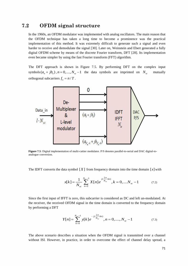
71
7.2 OFDM signal structure
In the 1960s, an OFDM modulator was implemented with analog oscillators. The main reason that
the OFDM technique has taken a long time to become a prominence was the practical
implementation of this method. It was extremely difficult to generate such a signal and even
harder to receive and demodulate the signal [30]. Later on, Weinstein and Ebert generated a fully
digital OFDM scheme by means of the discrete Fourier transform, DFT [28]. Its implementation
even became simpler by using the fast Fourier transform (FFT) algorithm.
The DFT approach is shown in Figure 7.5. By performing DFT on the complex input
symbols ( )n na jb , 0,...., 1scn N the data symbols are imprinted on scN mutually
orthogonal subcarriers /nf n T .
Figure 7.5: Digital implementation of multi-cattier modulator. P/S denotes parallel-to-serial and DAC digital-to-
analogue conversion.
The IDFT converts the data symbol [ ]X from frequency domain into the time domain [ ]x with
21 ( )
0
1[ ] [ ] , 0,.... 1
sc
sc
N j knN
sc
nsc
x k X n e k NN
(7.2)
Since the first input of IFFT is zero, this subcarrier is considered as DC and left un-modulated. At
the receiver, the received OFDM signal in the time domain is converted to the frequency domain
by performing a DFT
21 ( )
0
[ ] [ ] , 0,...., 1sc
sc
N j knN
sc
k
Y n y k e n N
(7.3)
The above scenario describes a situation when the OFDM signal is transmitted over a channel
without ISI. However, in practice, in order to overcome the effect of channel delay spread, a

72
special guard interval is inserted in each OFDM symbol referred to as cyclic prefix (CP). The
cyclic prefix is formed by appending CPN symbol of OFDM symbol sequences from the back to
the beginning of the sequence as illustrated in Figure 7.6. The receiver is instructed to ignore the
first CPN received samples and only the rest of the samples are demodulated by the FFT which
are unaffected by the channel response. Usually, the cyclic prefix is set longer than the maximum
delay spread of channel. Since it does not contain useful data it reduces the spectral efficiency.
In addition, there exists another method to remove the effects of the multipath channel, named
zero-padding (ZP). The only difference between ZP and CP is that CP is replaced with appending
zeros at the end of the symbol. ZP is also able to remove ISI when the length of appended zeros is
longer than the maximum delay of the channel. It is claimed in [27], ZP-OFDM outperforms CP-
OFDM in terms of better bit error rate (BER) performance and lower peak to average power ratio.
Because when the ZP prefix replaces the CP in OFDM symbols, the ripples in the power spectral
density can be reduced significantly.
Figure 7.6: Generation of cyclic prefix guard interval
A simplified block scheme of OFDM is shown in Figure 7.7. The signal in frequency domain is
denoted by capital letter and in time domain by small letter. ICP and RCP stand for insertion and
removal of cyclic prefix respectively.
Figure 7.7: Simplified OFDM transmitter and receiver blocks

73
7.3 Advantages of OFDM
The main advantages of OFDM which differentiates it from a single carrier modulation are:
Its robustness against frequency selective fading of the channel because of dividing the
channel bandwidth into many narrow sub-bands.
Mitigation of ISI by inserting cyclic prefix.
High bandwidth efficiency due to overlapping of subcarriers which result in higher data
rate transmission.
7.4 OFDM challenges
Below we will explore challenging issues in OFDM system and introduce potential method to
improve these disadvantages.
7.4.1 Peak to average power ratio (PAPR)
One of the major disadvantages of OFDM is its experience of large peak to average power ratio
when all subcarriers are added up coherently. If the transmitter contains a nonlinear power
amplifier then high PAPR forces it to operate in nonlinear region causing signal distortion. If the
linearity cannot be fulfilled, it causes both in-band and out-of-band interference to signals. The in-
band interference degrades system performance and the out-of-band interference causes adjacent
channel interference (ACI) that disturbs systems working in the neighbor bands [29]. However,
ACI does not occur in optical communication, because there are no applications in the
neighboring frequency bands and IR radiation is blocked by the walls. Systems with high PAPR
require power amplifier with a large dynamic range equal to the PAPR for distortion less
transmission which decreases amplifier efficiency. Therefore, reducing PAPR is necessary [29].
The PAPR is defined as the ratio of the maximum power occurring in OFDM symbol to the
average power of the same OFDM symbol.
2
2
max | ( ) |
[| ( ) | ]
x tPAPR
E x t (7.4)
where E [.] denotes expectation.
PAPR is mainly dependent on the number of subcarriers and selected digital modulation scheme.
As mentioned earlier, its maximum value occurs when all subcarriers are added coherently. In that
case, the maximum PAPR is scN for scN subcarriers [9]. However, in practice, full coherent
addition of all subcarriers is highly improbable. Therefore, although it is good to have a large
number of subcarriers to keep the overhead associated with cyclic prefix down, a large PAPR is a
significant penalty for large scN .
A large amount of research has been done to reduce PAPR of OFDM signal which are briefly
discuss in the following section.

74
7.4.1.1 PAPR reduction method
Generally, PAPR reduction techniques are categorized into two groups, the distortion based
techniques and the redundancy techniques. Clipping is a simple example of the distortion based
technique which limits the time-domain signal for which the signal power goes beyond a certain
threshold [30]. Clipping results in out of band radiation and poor error performance due to the
distortion of the original signal. The redundancy based techniques are categorized into the
following groups: coding, selective mapping and tone reservation, etc.
In selective mapping (SLM), a set of sequences from the original signal are generated and then
the sequence with the lowest PAPR is selected to transmit. Usually, transmission of side
information is required to inform the receiver which pattern is selection by transmitter, and then
the receiver can recover the information. The reliability of the side information has to be
considered [30].
Another popular method is tone reservations (TR) in which some of subcarriers are reserved to
reduce the peak power. These reserved subcarriers don’t carry any information. TR does not need
transmission of side information as in SLM. However, the receiver has to know the position of the
reserved subcarriers and ignores them. There are many strategies discussed in the literature to find
the proper subset of subcarriers, or reduce the computational cost for searching the best results.
The complexity is one serious drawback of TR. In addition, this set has to be calculated for every
OFDM frame individually [31].
Active constellation extension (ACE) reduces PAPR by changing the signal constellation without
affecting the BER performance. The challenge in this method is to find a unique way to map the
input data to the constellation point. The inverse process is needed to be implemented in the
receiver as well which is quite complex [32].
Coded OFDM is another promising technique which has received high attention due to its
capability to contest with multipath fading. The concept of the method is to apply those code
words that generate low PAPR. Besides, it can easily correct the errors due to frequency selective
fading. The use of coding for PAPR was a brilliant idea and realized by Jones, Wilkinson and
Barton [33].
The performance of TR and SLM are compared in [31] in which SLM presents better PAPR
reduction and power efficiency. TR suffers from lower power efficiency due to optimization
problems for tone reservation. In [29] turbo coding and selective mapping are used together to
reduce PAPR. The turbo encoder is applied to generate SLM sequences and it offers two
advantages of significant reduction in PAPR and bit error rate. It showed this combination can
reduce the probability of the PAPR exceeding 7dB from 70% to 0.25 % for a bit error rate =510 ,
SNR= 4dB and 128 subcarriers. Combination of selective mapping and clipping techniques are
applied to OFDM in [34]. If there is no error in the side information of SLM selected sequence,
then SLM does not cause any distortion affecting the error performance. Clipping causes an
effective reduction in PAPR but results in a large BER performance degradation. Therefore,
combining these two methods result in effective PAPR reduction and reasonable BER
performance.

75
In an optical Multicarrier (MCM) system, the main drawback is poor optical average power
efficiency. “Because the MCM electrical signal is a summation of modulated sinusoids and takes
on both negative and positive values, optical intensity (instantaneous power) must be nonnegative.
Hence, a DC bias must be added to the MCM electrical signal in order to modulate it onto the
intensity of an optical carrier. As the number of subcarriers increases, the minimum value of the
MCM electrical signal decreases (becomes more negative) and the required DC bias increases.
Since the average optical power is proportional to this DC bias, the optical average-power
efficiency worsens as the number of subcarriers increases “[35], [36].
Therefore, many techniques used to reduce PAPR in a RF system are insufficient to reduce the
DC bias in an optical MCM system [35]. The impact of large DC biasing influences the choice of
the LED operating point. There are a few techniques introduced to reduce PAPR and DC biasing
of an optical MCM system.
Reference [35] discusses two classes of techniques for reducing the optical average power
requirement in MCM with IM/DD system. The first class of techniques involves block coding
between the information bits to be transmitted and the symbol amplitudes modulated onto
subcarriers. The second class of techniques involves replacing the fixed DC bias by a bias signal
that varies on a symbol-by-symbol. Reference [36] also proposes two techniques to reduce the
average optical power in wireless optical MCM systems, namely in-band trellis coding and out-
of-band carrier design.
7.4.2 Frequency and timing offset
As shown in Figure 7.3, the input data is modulated onto orthogonal subcarriers separated by
subcarrier spacing f and these subcarriers overlap in the frequency domain. However, in
practice, the frequency orthogonality is not perfect due to time synchronization error, Doppler
frequency shift and oscillator mismatch [9]. Synchronization of an OFDM signal is important step
at the receiver because if it is not performed very accurately the orthogonality between subcarriers
is lost resulting in inter-carrier interference (ICI).
Sensitivity to frequency and timing offset is higher in multicarrier system. When the number of
subcarriers grows, it forces OFDM symbol time to be larger which causes the subcarriers to be
closer together. Narrower sub-bands are more susceptible to ICI.
A wide variety of techniques have been proposed for estimating and correcting both time and
frequency offsets at OFDM receiver. Some of these techniques are introduced in the following
section.
7.4.2.1 Timing and frequency synchronization techniques
OFDM synchronization methods are categorized into data-aided and non-data-aided groups. In
the data-aided category, a training sequence or pilot symbols are used for estimation. It is highly
accurate and simple; however, it wastes bandwidth and reduces data transmission speed. On the
other hand, the non-data aided category uses the cyclic prefix for estimation. Reduction in
bandwidth efficiency is less compared to data-aid category but it does not have high accuracy in
estimation [37].
76
Schmidl and Cox [38] proposed a method for time and frequency synchronization by using two
training symbols placed at the start of the frame. The first symbol has two identical halves in the
time domain. The correlation between these two halves can be performed to find the beginning of
the symbol and then, the carrier frequency offset is corrected.
Nogami and Nagashima [39] presented an algorithm to find time and frequency offset by using a
null symbol. In this symbol period, nothing is transmitted so that the received power is dropped
and it can be detected to find the beginning of the frame.
Beek and Sandell [40] described a method which jointly finds both time and frequency offset
called joint maximum likelihood estimator (ML). In this method, redundant information is
contained within cyclic prefix which enable the estimation without additional pilot.
7.5 Summary
In this chapter we have studied the effect of the channel on a single and multicarrier system. In
multicarrier system, dividing the serial data stream to the number of parallel data streams brings
two advantages: first, due to the decreasing symbol rate on each sub-channel, the probability that
the symbol being completely corrupted in a fading channel is reduced. Second, the narrow sub-
channel diminishes the need for a channel equalizer. In addition, using multilevel digital
modulation on each subcarrier increases transmission data rate. In OFDM, the major advantage is
that the interference is reduced by applying a cyclic prefix. OFDM has two main drawbacks
which affect the performance of the system: frequency offset and high PAPR. However, many
methods have been introduced to improve the impairments of OFDM. For example coded and
clipping OFDM are the promising alternatives in multipath and fading environment. For an
optical MCM with large number of subcarriers, besides a high PAPR, requirement of a large DC
biasing to drive the optical source is a major concern. Due to the limitation in generating a large
DC bias, the number of subcarriers cannot be increased infinitely to compensate cyclic prefix
overhead or to increase the data rate in an optical MCM system.
77
8.
Modulation choice for the
system
This chapter starts with calculation of data rate for supporting 100 audio channels for
infrared language distribution system. We will compare and analyse the application of
single and multi-cattier modulation for the system according to methods introduced in
previous chapters and show how the results differ for each approach. To that end, there is
a brief discussion on the challenges of the selected approach for the system design.
In chapter 2 and 3, we discussed the different aspects of wireless optical communication and a
method for evaluating the impulse response of the infrared channel. Therefore, the maximum
delay spread and RMS delay of the channel was determined based on ray-tracing simulation
model, where are found 400ns and 100ns, respectively, for a room with size of 2600m². In
chapters 4 and 5, we demonstrated the feasibility of increasing the bandwidth of the system from
8MHz to 18MHz with applying new opto-electrical components. In this chapter, depending on the
characteristics of the channel and system requirement we are going to compare different
modulation schemes and select the option which proves a better fit than others.
As mentioned in chapter 1, the current system supports 32 audio channels in bandwidth between 2
and 8MHz with 8 non-overlapping subcarriers. For each subcarrier DQPSK modulation and
raised cosine pulse with factor Nr = 0.4 are applied. Each subcarrier has a bandwidth of 586.53
kHz; therefore, the data rate per transmission channel is given by
2 586.53
837.9(1 ) 1.4
b
N
B l kHzR kbps
r
(8.1)
The total data rate 32 channels is 8*837.9kbps= 6.7Mbps.
8.1 General system requirement
The next generation of the Bosch infrared language distribution system needs to support 100
audio channels. To realize a larger number of audio channels, it is needed to increase the data rate
of the overall system. As mentioned before, there exist two options to increase the data rate of the
system. First, increase the currently used bandwidth and second, make a more efficient use of the
available bandwidth. In case of the first option, the current bandwidth of the system can be
increased to 18MHz. In case of the second option; several techniques were discussed such as
higher order digital modulation and multicarrier modulation.

78
In the following, a simple calculation is set up to define the total data rate required for a system
supporting 100 audio channels. The sampling frequency ( sf ) and Reed-Solomon (RS) code are
chosen equal to those applied in the current system. Therefore, the raw bit rate corresponding to
each audio channel is given by
1
r s wd
c
R f nR Cf
(8.2)
where sf = 44.1 kHz is sample frequency, wdn = 16 sampling word, cR = 24/28 is the coding rate
and Cf = 4 is compression factor. Thus, the total data rate for 100 audio channels is given
100 20.58 /T rR R Mb s (8.3)
To make it more clear, Figure 8.1 shows the raw data rate generated in each stage at transmitter
side before modulation is applied.
Figure 8.1: Raw data rate in different stages of transmitter
8.2 Single carrier approach with multilevel modulation
When a signal is wideband and symbol duration is less than the RMS delay spread. In that case, if
the signal is transmitted over a multipath channel, each of the different multipath components will
interfere with subsequently transmitted symbols and generate ISI.
From chapter 2, the maximum delay spread and RMS delay were considered to be 400ns and
100ns respectively. Therefore, the modulated signal experiences negligible ISI if the symbol rate
is limited to 1/10 1 /s RMSR Msymbol s .
Consequently, the large RMS delay spread creates a significant constraint on the data rate of the
system. To increase the data rate in such approach, a high level modulation method must be used.
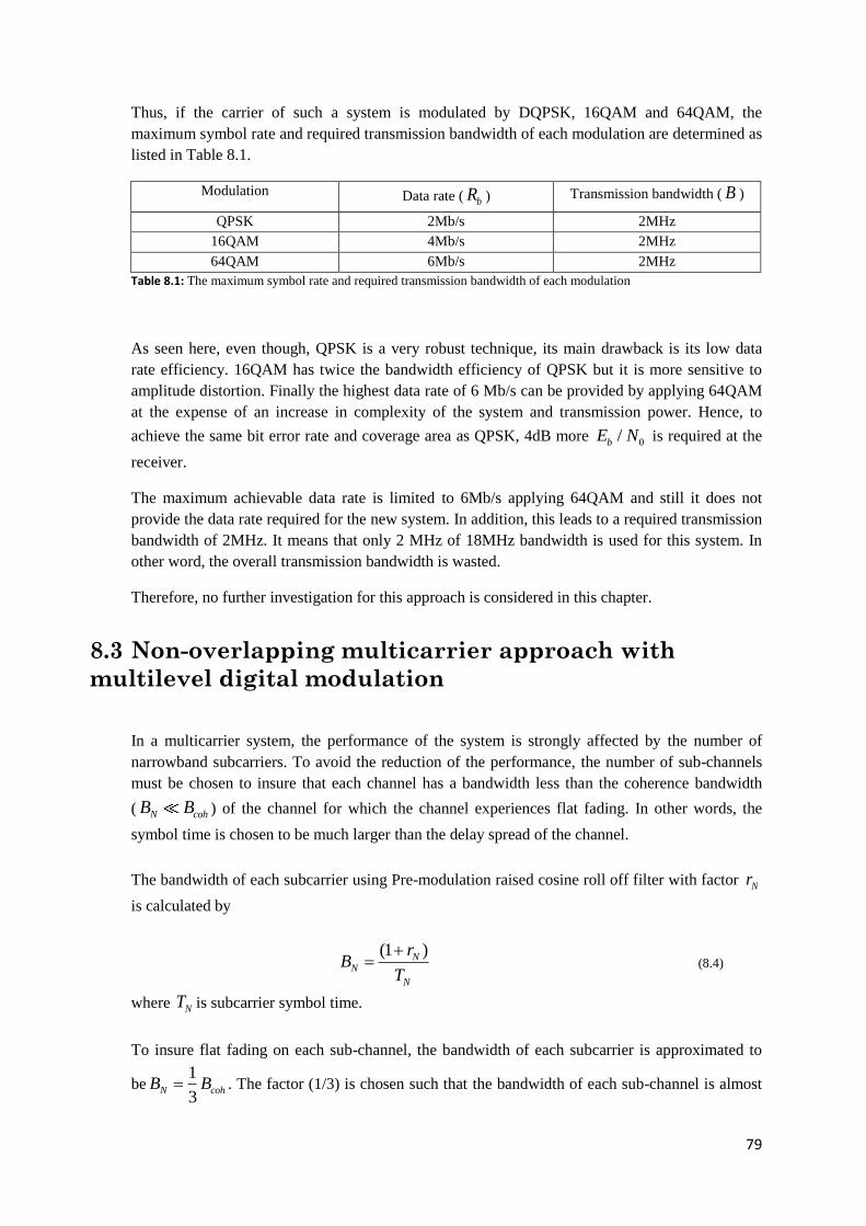
79
Thus, if the carrier of such a system is modulated by DQPSK, 16QAM and 64QAM, the
maximum symbol rate and required transmission bandwidth of each modulation are determined as
listed in Table 8.1.
Modulation Data rate ( bR ) Transmission bandwidth ( B )
QPSK 2Mb/s 2MHz
16QAM 4Mb/s 2MHz
64QAM 6Mb/s 2MHz
Table 8.1: The maximum symbol rate and required transmission bandwidth of each modulation
As seen here, even though, QPSK is a very robust technique, its main drawback is its low data
rate efficiency. 16QAM has twice the bandwidth efficiency of QPSK but it is more sensitive to
amplitude distortion. Finally the highest data rate of 6 Mb/s can be provided by applying 64QAM
at the expense of an increase in complexity of the system and transmission power. Hence, to
achieve the same bit error rate and coverage area as QPSK, 4dB more 0/bE N is required at the
receiver.
The maximum achievable data rate is limited to 6Mb/s applying 64QAM and still it does not
provide the data rate required for the new system. In addition, this leads to a required transmission
bandwidth of 2MHz. It means that only 2 MHz of 18MHz bandwidth is used for this system. In
other word, the overall transmission bandwidth is wasted.
Therefore, no further investigation for this approach is considered in this chapter.
8.3 Non-overlapping multicarrier approach with
multilevel digital modulation
In a multicarrier system, the performance of the system is strongly affected by the number of
narrowband subcarriers. To avoid the reduction of the performance, the number of sub-channels
must be chosen to insure that each channel has a bandwidth less than the coherence bandwidth
( N cohB B ) of the channel for which the channel experiences flat fading. In other words, the
symbol time is chosen to be much larger than the delay spread of the channel.
The bandwidth of each subcarrier using Pre-modulation raised cosine roll off filter with factor Nr
is calculated by
(1 )N
N
N
rB
T
(8.4)
where NT is subcarrier symbol time.
To insure flat fading on each sub-channel, the bandwidth of each subcarrier is approximated to
be1
3N cohB B . The factor (1/3) is chosen such that the bandwidth of each sub-channel is almost

80
the same as the sub-channel bandwidth of the current system. The coherence bandwidth is
1/ 2coh RMSB = 1.6 MHz with respect to 100ns RMS delay spread. So the resultant bandwidth
of each sub-channel is
1 1
1.6 1.4 5333 3
N cohB B MHz kHz (8.5)
Consider multicarrier system with transmission bandwidth of TB = 18MHz and bandwidth of
NB = 533 kHz per each sub-channel, then number of sub-channel ( scN ) is determined by
/ 18 / 560 33sc T NN B B MHz kHz (8.6)
Total data rate of the system with QPSK modulation (l=2) on each carrier is given by
533 2
33 25 /1 1.4
Nb sc
N
B l kHzR N Mb s
r
(8.7)
If subcarriers are modulated by 16QAM then data rate increases to bR =50Mb/s.
8.3.1 Effective bandwidth per carrier
In a realistic implementation, a sub-channel will occupy a larger bandwidth than under ideal
raised cosine pulse shaping. It is because from the total bandwidth, a factor of x is reserved as
guard band ( GB ) between subcarriers and it discards the imperfect matching of the filters in
transmitter and receiver. The factor x denotes the sum of all the guard bands relative to the total
bandwidth, so:
0 1,G TB x B with x (8.8)
Then, the actual available bandwidth considered for data transmission is
(1 )avail T G TB B B x B (8.9)
The efficient bandwidth and available data rate per subcarrier are obtained by
(1 )
,1
Teff b eff
sc N
x B lB R B
N r
(8.10)
where scN is number of subcarrier.
81
Using x = 0.2 as considered in the design of the current system results in available bandwidth of
availB =14.4MHz. Considering effB = 533 kHz as efficient bandwidth per carrier results in 27
subcarriers. In this case, with QPSK per carrier, the total data rate is
533 2
27 20 /1 1.4
eff
b sc
N
B l kHzR N Mb s
r
(8.11)
As seen from (8.7) and (8.11), this approach can provide the required data rate of the new system.
However, due to the guard band insertion, there is a large reduction in bandwidth efficiency. In
addition, implementation of this method requires separate modulators and demodulators for each
subcarrier which make the system design rather complex for a large number of subcarriers.
8.4 OFDM approach
The OFDM scheme has been discussed in details in previous chapter. Briefly, in OFDM, the input
data stream is divided into data blocks of size scN where each block is referred to as an OFDM
symbol. A cyclic prefix is added to each OFDM symbol to eliminate ISI between the data blocks.
The spectral efficiency increases due to overlapping of sub-channels and it is easily implemented
with performing of IFFT and FFT.
8.4.1 OFDM system parameters
The key parameter to start the design of an OFDM system is maximum channel delay spread
which was determined to be 400ns ( max ). Therefore, the guard interval must be at least as long
as max . We choose the guard time to be about gT = max2 so that the design is sufficiently immune
against delay spread variation. The useful symbol duration ( uT ) of an OFDM block is equal to
inverse of the subcarrier spacing ( f ).
When the subcarrier spacing increases, then automatically the symbol period decreases. It is
desirable to have symbol duration much larger than the guard time to compensate the overhead of
the guard interval. However, it can’t be arbitrarily large because large symbol duration means
more subcarriers, small subcarrier spacing and more sensitivity to frequency offset. Also there is
an increase of the peak to average power ratio. In addition, for an optical OFDM system, more
subcarriers result in large DC biasing which means poor average optical power efficiency.
By referring to the literature, typically, useful symbol period is u gT T for which = {4, 8, 16,
32}. After adding the guard interval, the actual duration of an OFDM symbol is OFDM g uT T T .
The total data rate of an OFDM system is now calculated by
1
b OFDM data c
G u
R N l RT T
(8.12)
82
where l is number of bits per modulated symbol, dataN
number of subcarriers for data
transmission and cR is the coding rate (24/28).
To calculate the achievable data rate, the guard interval, number of bit per symbol and coding rate
are known. Therefore, this equation shows a tradeoff between number of subcarrier and useful
symbol time.
In OFDM, usually, not all subcarriers of an OFDM are used for data transmission. There are four
types of subcarrier
Data subcarriers ( dataN ): useful data transmission.
Pilot subcarriers (pilotN ): as discussed in (5.5.1) they are mainly used for channel
estimation and synchronization.
Null subcarriers ( nullN ): these subcarriers usually are near two edges of the assigned
band. No information is transmitted by these subcarriers and they are only used to prevent
significant leakage to adjacent band. They are also known as guard subcarriers or virtual
subcarriers. When the OFDM signal power spectrum has high side lobes, generation of
this guard band helps to reduce the out of band emission and thus eases the requirement
on transmitter front-end filters. Insertion of guard bands wastes some assigned bandwidth
and decreases spectral efficiency of the OFDM system [41].
DC subcarrier: it is a subcarrier whose frequency is equal zero.
Therefore, the total number of subcarrier used for transmitting a modulated data symbol
is 1data ifft pilot nullN N N N .
Returning to the OFDM system analysis, in order to exploit the channel bandwidth in an efficient
way, no pilot and null subcarriers are considered for synchronization and frequency band,
respectively. Pilot subcarriers are not necessary because the optical wireless channel changes very
slowly and Doppler frequency is considered zero. Thus, a reference symbol can be used for
channel estimation and synchronization. As the channel is assumed to be only very slowly time-
varying, this reference symbol can be transmitted every n symbols and causes an overhead. In
addition, null subcarriers are not required because in optical wireless communication, there is no
application in the adjacent frequency band. The parameters of an OFDM system for different
values of are calculated and listed in Table 3.

83
4 8 16 32
Overall bandwidth (MHz) 18 18 18 18
Guard interval (ns) 800 800 800 800
Useful symbol duration(μs) 3.2 6.4 12.8 25.6
OFDM symbol duration (μs) 4 7.2 13.6 26.4
Subcarrier spacing (kHz) 312 156 78.12 39.6
Number of data subcarrier 57 115 230 460
Number of bits per symbol 2 2 2 2
OFDM data rate (Mbps) 24.42 27.3 28.99 32.16
FFT size 64 128 256 512
Cyclic prefix overhead 20% 11% 5.9% 3%
Table 8.1: QPSK-OFDM parameters
We have proposed an OFDM system with different number of subcarriers. We have considered
optical channel properties to determine guard interval and the useful symbol duration of OFDM.
It was also considered to transmit low information redundancy such as pilot insertion. Therefore,
since the chosen design of opto-electrical front-ends allows the bandwidth of 18 MHz, if QPSK
modulation is applied on each subcarrier, it can fulfill the required data rate for the new system.
In addition, QPSK is a good option for optical channel because it is less sensitive to high channel
path loss.
As mentioned before, the larger the number of subcarriers, the greater the symbol period on each
carrier leading to higher bandwidth efficiency and a smaller cyclic prefix overhead. On the other
hand, the large number of subcarriers results in high PAPR, large DC biasing required for optical
source and the complexity in the implementation increases. As seen in Table 8.2, an OFDM with
57 data subcarriers, carrier spacing of 312 kHz and 64IFFT can provide the data rate of 24Mbps
with small number of subcarriers. Therefore, all mentioned reasons result in the choice for the
size of 64FFT.
Later in this chapter, the challenges with the selected option are investigated.
8.4.2 Challenges with chosen OFDM parameters
Based on the system constraints and channel information, chosen method faces some issues in the
design which are discussed briefly in the following
Linearity of the optical source
For wireless optical systems, since the OFDM modulating signal at the LED input is a sum of
dataN signals on equidistant subcarrier frequency, then the amplitude of modulating signal may
exceed the maximum value defined for linearity of the LED. However, As long as the linearity is
achieved, having large number of subcarrier is minor issue. Therefore, whether LED output power
experience distortion if an OFDM signal (summation of 57 subcarriers) is transmitted must be
checked.

84
Peak to average power ratio
Multicarrier systems suffer from a high peak to average power ratio due to the addition of many
independent frequency carriers. This results in nonlinear distortion due to clipping in transmitted
signal. If the modulated signal at the LED input is a sum of dataN = 57 signals on equidistant
subcarrier frequencies with equal amplitude, the maximum PAPR is approximately given by [9]
1010log ( 57)dataPAPR N =17.55 dB (8.13)
This value is still high and PAPR reduction methods are still of great interest because if the PAPR
is reduced then more average power can be transmitted and it means increase in the coverage
area. Figure 8.2 shows PAPR for proposed OFDM parameters listed in Table 8.2 when they
transmit same data rate.
Figure 8.2: PAPR vs. Number of subcarriers
Average optical power requirement
As said earlier, transmission of the optical multicarrier signal is translated in a requirement for a
large DC signal which in turn implies a large average optical power requirement. Many
approaches proposed in literature to improve the power efficiency (in terms of DC) are based on
block-coding and other techniques proposed for RF OFDM. Nevertheless, these techniques
reduce the transmission rate and may have large implementation complexity like TR or SLM.
The power penalty for a multicarrier MQAM modulation is determined by [1]
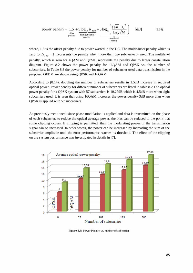
85
10 10
offsetmulti-subcarrier penalty penalty
multi-level penalty
2( 1)
log2
1.5 5log 5log [ ]data
M
Mpower penalty N dB
(8.14)
where, 1.5 is the offset penalty due to power wasted in the DC. The multicarrier penalty which is
zero for 1dataN , represents the penalty when more than one subcarrier is used. The multilevel
penalty, which is zero for 4QAM and QPSK, represents the penalty due to larger constellation
diagram. Figure 8.2 shows the power penalty for 16QAM and QPSK vs. the number of
subcarriers. In Table 8.3 the power penalty for number of subcarrier used data transmission in the
purposed OFDM are shown using QPSK and 16QAM.
According to (8.14), doubling the number of subcarriers results in 1.5dB increase in required
optical power. Power penalty for different number of subcarriers are listed in table 8.2.The optical
power penalty for a QPSK system with 57 subcarriers is 10.27dB which is 4.5dB more when eight
subcarriers used. It is seen that using 16QAM increases the power penalty 3dB more than when
QPSK is applied with 57 subcarriers.
As previously mentioned, since phase modulation is applied and data is transmitted on the phase
of each subcarrier, to reduce the optical average power, the bias can be reduced to the point that
some clipping occurs. If clipping is permitted, then the modulating power of the transmission
signal can be increased. In other words, the power can be increased by increasing the sum of the
subcarrier amplitude until the error performance reaches its threshold. The effect of the clipping
on the system performance was investigated in details in [7].
Figure 8.3: Power Penalty vs. number of subcarrier

86
Transmission power and coverage area
The ratio of the received signal to the noise (SNR) at the receiver output is the most important
factor in designing a system. Hence, it is necessary for a receiver to achieve a certain level of
signal to noise ratio which it is given by
0 0
b r
b
E P
N N R (8.15)
where, rP is received electrical power and 0N is noise spectral density. The received LOS optical
power was determined by Eq. (2.6). The received electrical signal after (amplifying assuming
trans-impedance amplifier) is given by
2
2
( 1) cos ( )cos ( )[( ) ] [ ]
2
n m
elec t p f
n AP P R R W
r
(8.16)
where, TP is transmitter optical power,
pR is the responsivity of the receiver (A/W) , r is distance
between transmitter and receiver and fR is feedback resistor of trans-impedance amplifier.
Therefore, by substituting (8.14) into (8.13)
2
2
( 1) cos ( )cos ( )[( ) ]
2
n m
b b t p f
n AE R P R R
r
(8.17)
Eq. (8.17) shows that increasing the data rate of the system and keeping both coverage area and
transmitted power similar to the current system, the received energy per bit decreases significantly
resulting in high bit error rate. Therefore, to obtain the same energy per bit at receiver, either
transmitted power must be increased or the coverage area decreased. In the proposed OFDM
model, the transmission data rate is approximately b OFDMR =24Mb/s which is almost three times
more than that in current system. This results in power penalty of 5dB for new system to achieve
the same performance as current system. In addition, as shown in Figure 8.3 increase in the
number of subcarriers results in 4dB power penalty. Therefore, total power penalty due to large
number of subcarriers and high data rate transmission is 9dB. Number of subcarriers and high
data rate transmission also affect converge area. Increase in data rate from 6.7Mbps to 24Mbps
leads to reduction of 0.5 in coverage area and increase in the number of subcarrier leads to
reduction of 0.33 in coverage area.
On the other hands, it can be observed that the received power depends on area and responsivity
of the detector as well as gain of the amplifier. Using a detector with large area and good
responsivity provides more power at receiver without the need of large increase in transmitted
power.
87
9.
Conclusion and further
research
9.1 Conclusion
This thesis provides system design in order to increase the data rate of wireless infrared multi
language distribution system. In short the results of this thesis confirm that it is possible to
increase the data rate of the system and OFDM is a suitable method for the system whose
parameters can be tailored according to the system requirement. To make OFDM less
sensitive to optical channel loss and have low PAPR, we offered OFDM with small number of
subcarriers and phase modulation on each subcarrier. As seen in chapter 8, OFDM with 57
subcarriers for data transmission, 64IFFT size and QPSK modulation can provide the required
data rate of the new system. The contributions of this thesis work are summarized as follows:
Firstly, single and multi reflection optical channel for any room size and any transmitter
and receiver configurations are modelled by using ray- tracing model. The results show
reasonable agreement with the simulation model of Philips. In single reflection model,
received power, maximum delay spread and RMS delay spread with respect to power
level of -30dB and -40dB as a threshold of the received signal are determined. In multiple
reflection models, the same parameters are found with considering limited number of
second reflections; it shows that considering second reflections slightly increase amount
of received power and also there is an increase in excess delay due to second reflections
from far away reflectors. Therefore, based on the simulation results, the single
reflection paths have the most effect on the characteristics of the optical channel.
The important parameters of the multipath optical channel have been determined,
the maximum delay spread of 400ns and RMS delay of 100ns which affect the choice
of applying multicarrier or single carrier modulation.
Opto-electrical front-ends are analyzed and their relevant components and parameters are
discussed in order to achieve a design as simple as possible, which allows a wide
transmission bandwidth. A simple measurement set up is used to determine whether the
frequency bandwidth represented on the datasheet of components can be achieved in
different distances. At the transmitter side, LED (TSFF5410) is chosen as a transmitter.
At the receiver side, a PIN diode (TESP5700) and a preamplifier (OPA847) are
considered as main components. The discussion of the opto-electrical front-ends is not
intended to optimize the receiver design, but aimed to provide a set of realistic receiver
parameters useful for further investigations. The desired bandwidth of 18 MHz resulted
from the choice of the source, detector and preamplifier types. It is clear that the

88
transmission bandwidth of the current system is limited by the bandwidth of the
photo-detector.
Theoretical approaches for increasing the data rate of the system are investigated by
comparing several modulation techniques in terms of bandwidth and power efficiency. The
result shown that single carrier modulation with even 64QAM modulation in the bandwidth
of 18MHz cannot provide the required data rate of the system. Therefore, no more
investigation is considered for this approach. From analysis of a non-overlapping multicarrier
approach for the system, it is represented that a multicarrier system is defined with 33 sub-
channels and bandwidth of 533 kHz for each sub-channel. In this case, the transmission data
rate of the system using QPSK is 25Mbps. In addition, it was discussed that in a realistic
implementation, a guard interval is inserted between each sub-channel in order to discard the
imperfect matching in transmitter and receiver filters. In this case, if 3.6MHz of the
bandwidth is considered as overall guard band, the available bandwidth and number of
subcarriers are decreased to 14MHz and 27, respectively. Then the data rate of the system
decreases to 20Mbp. Consequently, although this approach can provide the required data rate
to support 100 audio channels, the implementation of this method requires separate
modulators and demodulator for each subcarriers which the system design becomes rather
complex for large number of subcarriers. Therefore, the single carrier and non-
overlapping multicarrier modulation are not good approaches to increase the data rate
of the system because of low bandwidth efficiency and high complexity.
Finally, the OFDM approach is introduced as a good option for the system. Deployment of
OFDM in an optical wireless system brings various benefits, among which are providing
large bandwidth efficiency with simple front-end design and its robustness to frequency
selective fading response. The influence of OFDM on peak to average power ratio, optical
power penalty, large DC basing for optical MCM system are discussed. Since the chosen
opto-electrical front-ends allow a signal bandwidth of 18MHz, the choice for 64 IFFT
with 57 subcarriers for data transmission, guard interval twice the maximum delay
spread of the optical channel and QPSK modulation on each subcarrier can achieve the
transmission data rate of 24Mbps with small number of subcarriers. Therefore, among
analyzed methods, OFDM is a better option due to make efficient use of the bandwidth
and simple implementation.
In addition, the increase in transmission data rate results in a reduction in the received
energy per bit to achieve the same coverage area and transmitted power as the current
system. Therefore, to obtain the same performance as current system, either transmitted
power must be increased or the coverage area decreased.

89
9.2 Further work
There are fundamental recommendations for further research:
The optical channel model is defined for a limiting number of second reflections;
therefore, further work on the modeling of the channel can improve the accuracy of the
model even considering third and fourth order reflections. Despite the advantages of the
simulation, many issue can only be resolved through an experimentation for example, the
model is applied for an empty room; however, objects in the room must be taken into
account with which impulse response varies. Therefore, it is necessary to obtain impulse
channel characteristics by measurement.
The measurement set up to determine transmission bandwidth of the new opt-electrical
components is performed when distances between transmitter and receiver are 2cm, 5cm
and 10cm. It can be shown that the same bandwidth can be achieved for larger distances
if more than one LED or PIN diodes are used. Especially, since the PIN diode is the
bandwidth limiting factor, by using 2 PIN diodes, the amount of the reduction in the
bandwidth for the introduced receiver front-end can be viewed.
The investigations conducted in OFDM analysis is based on the theoretical calculation,
therefore, another important step in future work that can be accomplished is to determine
the permitted power of the LED that it does not experience distortion when an OFDM
signal (summation of 57 subcarriers) is transmitted which it can be used to determine the
level of the permitted clipping
In this work many methods are introduced to reduce PAPR and it was not foreseen that
which method is a suitable option for optical OFDM system and how much they can
reduce PAPR. However, according to many references the suitable PAPR reduction
method for an optical OFDM system is clipping. Therefore, the effect of the clipping on
BER can be evaluated.
The last interesting topic would be to implement the OFDM transmitter and receiver.
91
10.
References
[1] Barry, J. (1986). Wireless Communication Using Non-Directed Infrared Radiation. University
of California.
[2] Ramirez, R., & Green, R. J. (1999). Indoor Optical Wireless Communications. London: IEE,
Savoy Place.
[3] Kahn, J., & Barry, J. (1997). Wireless INfrared Communication. Proceeding of the IEEE, 265-
298.
[4] Singh, C., & John, J. A Review on INdorr Optical Wireless System.
[5] Gfeller, F., & Bapst, U. (1997). Wireless In-house Data Communication via Diffuse INfrared
Radiation. IEEE , 1472-1492.
[6] Kahn, J., & You, R. (1998). Imaging Diversity Recievers for High-Speed Infrared Wireless
Communication. IEEE Communication magazine .
[7] Grubor, J. (2009). Adaptive Modulation Technique for Broadband Communication in Indoor
Optical Wireless Systems. Berlin. Berlin: Technical University of Berlin.
[8] Hashemi, H. (1994). Indoor Propagation Measurement at infrared frequency for wireless local
area network applications. Vehicular Technology, IEEE Transactions, 562 - 576
[9] Goldsmith, A. (2005). Wireless Communications. Cambridge University Press.
[10] Hernandez, L. (1997). Algorithm for calculation of impulse response on IR wireless indoor
channels. Electronic letters, IEEE, 1804 - 1806
[11] Lopez-Hernandez, F., & Perez, R. (1998). Monte Carlo calculation of impulse response on
diffuse IR wireless indoor channels. ELECTRONIC LETTERS , 1260-1262.
[12] Carruthers, J., & Kannan, P. (2002). Iterative Site-Based Modeling for Wireless Infrared
Channels. IEEE ANTENA AND PROPAGATION .
[13] lomba, C., & Valadas, R. Efficient Simulation of the Impulse Response of the Wireless
Optical Channel. Potugal.
[14] Moreira, A., & Valadas, R. (1997). Optical interference produced by artificial light. Wireless
Network , 131-140.
[15] Moreira, A., & Valadas, R. (1995). Characterisation and Modelling of Artificial Light
Interference in Optical Wireless Communication Systems. Torento: PIMRC.
[16] Mathias, J. (2007). eetimes. Retrieved from Wi-Fi Channel Emulation Goes Mainstream:
http://www.eetimes.com/design/rf-microwave-design/4012902/Wi-Fi-channel-emulation-goes-
mainstream

92
[17] Hranilovic, S. (2005). Wireless Optical Communication Systems. United State of America:
Springer.
[18] IEC. (1993). International Electro-technical Commission. Safety of laser products.
Equipment classification requirements and user's guide . Group safety publication.
[19] Retrieved from PHOTODIODE CHARACTERISTICS: http:\\www.udt.com
[20] T1A1, A. C. (2008). Retrieved from Noise-equivalent power:
http://en.wikipedia.org/wiki/Noise-equivalentpower
[21] Noise Specs Confusing. (n.d.). Retrieved from National Semiconductor.
[22] Wideband, Ultra-Low Noise, Voltage-Feedback Operational Amplifier with Shutdown. (n.d.).
Retrieved from Texas Instruments: www.ti.com
[23] Kim, S., & Lee, U. (2007). Improved Performance of APSK Modulation Scheme for
Sattellite System. Information, Communication and Signal Processing, IEEE, 1- 4.
[24] Ali, P., Hussain, F., & Jeong, G. (2008). . A low complexity De-mapping Technique for 16-
APSK Modulation for Digital Video Broadcasting in AWGN Channel. International Conference
on Convergence and Hybrid Information Technology. Seoul: Hanyang University.
[25] Sklar, B. (1993). Defining, Designing, and Evaluating Digital Communication Systems.
IEEE Communication Magazine .
[26] Sankar, K. (2008). Signal Processing for Communication. Retrieved from Comparing BPSK,
QPSK,16QAM, 16PSK, 64QAM and 32PSK: http://www.dsplog.com
[27] Lu, G., & Nikookar, H. (2009). On The Potential of ZP-OFDM for Cognitvie Radio.
Wireless Personal Multimedia Communication .
[28] Matiæ, D. OFDM as a possible modulation technique for multimedia applications in the
range of mm waves. In Introduction to OFDM.
[29] Abouda, A. (2004). PAPR REDUCTION OF OFDM SIGNAL USING TURBO CODING
AND SELECTIVE MAPPING. Nordic Signal Processing Symposium .
[30] Lin, M., Tsai, Y., & Yang, C. (2005). Selective-Mapping Type Peak Power Reduction
Techniques for Turbo Coded OFDM. IEEE .
[31] Siegl, C., & Fischer, R. (n.d.). Tone Reservation for Peak-to-Average Power Ratio Reduction
in OFDM under Different Optimization Constraints.
[32] Kumara, A., & Sim, M. (2008). PAR Reduction in Space-Time Coded OFDM via Modified
Active Constellation Extension. Innovative Technologies in Intelligent Systems and Industrial
Applications, (pp. 12-13). Malaysia.
[33] Zafar, Q., Taha, Q., & Xian, L. A PAPR REDUCTION TECHNIQUE USING
EXPURGATED CYCLIC CODES FOR COFDM,. Arkansas: University of Arkansas.
[34] Wang, L., Cho, K., & Yoon, D. PAPR Reduction of OFDM Signals Using Deliberate
Clipping and Pre-scrambling Technique. seoul: Hanyang University.
[35] You, Y., & Kahn, J. (2001). Power Reduction Techniques for Multiple-Subcarrier Intensity-
Modulated Optical Signals. Communications,IEEE, 1620 – 1627.
[36] Kang, W., & Hranilovic, S. (2008). . Power Reduction Techniques for Multiple-Subcarrier
Modulated Diffuse Wireless Optical Channels. Communcation, IEEE Transactions, 279 – 288.

93
[37] Wu, F., & Abu-Rgheff, M. Time and Frequency Synchronization Techniques for OFDM
Systems operating in Gaussian and Fading Channels. University of Plymouth.
[38] Schmidl, T., & Cox, D. (1997). Robust Frequency and Timing Synchronization for OFDM.
Communication, IEEE Transactions, 1613 – 1621.
[39] Nogami, H., & Nagashima, T. A frequency and timing period acquisition technique for
OFDM systems, Personal, Indoor and Mobile Radio Communication. PIRMC, (p. 1995).
[40] Beek, J., & Sandell, M. (1997). ML Estimation of Time and Frequency Offset in OFDM
Systems. IEEE Transactions on Signal Processing .
[41] Chiueh, T., & Tsai, P. (2007). OFDM baseband receiver design for wireless communication.
Singapore: Wiley.