ta-i company profile - tyeeusa.com profile.pdf · 2 company profile *established : jan.1986...
TRANSCRIPT

TA-I Technology Co., Ltd.
TA-I Company Profile

2
Company Profile
*Established : Jan.1986
*President : Mr. Paul Chiang
*Capital: US$ 80.3M (Listed Company)
*Revenue : 2010 $136M, 2011 $137M, 2012 $138M, 2013 $155M(F)
*Employees : 2,500 (Worldwide)
Service
24 hours per day, 7 days per week.
6 support offices, 6 manufacture bases.
One stop shopping for LED substrate / Res. / Chip fuse/ Current sensing /NTC/ESD/ MLV,...
Advantage
Excellent logistic service.
Quality Satisfaction.
Total Solution.
Environmental Protection.
Chip resistor capacity 2nd ranking in the world.

3
Worldwide Customer Support
Production
& Sales Office
Sales Only
Agent
Taiwan
SuZhou
(China)Dongguan
(China)
Los Angeles
(USA)
Penang
(Malaysia)
Jakarta
(Indonesia)
Seoul
(Korea)
(1) (2)

4
Product Line
High Voltage
Resistors
RH series
Current Sensing
Resistor
RLM, RLN, RLP,
RL, RBL Series
Chip Fuse
CF/CFS/CP/
CPS/TRF Series
NTC
MTR Series
ESD
SUPPRESSOR
UMS/MS Series
Thick Film
(RM series)
01005
0201
0402
0603
0805
1206
1210
2010
2512
Resistor Array
(CN series)
Convex type
Concave type
(0402, 0603)
4P2R
8P4R
10P8R
16P8R
Thin Film
(RB series)
0201
0402
0603
0805
1206
2010
2512
Circuit
ProtectionDiscrete Resistor
Ceramic Thermal
Dissipation
Substrate
Power
Passive
Resistor
Array
Customized
Heat dissipation
substrate
Ceramic carrier
board
HCPV board

5
Major Customers
Consumer
Communi-
cation
PC
Display
PC
Peripheral
EMS
Household
Application
Others

6
Major Customers (LED)
Approval
Mass Production
Sampling

7
FINANCIAL REPORT 1
Consolidated Balance Sheet
Provided by: TA-I TECHNOLOGY CO.,LTD
Financial year: Yearly
Unit:NT$ thousand
Accounting Title
9/30/2012 9/30/2011
Amount % Amount %
Assets
Current Assets
Cash and cash equivalents 852,999.00 13.38 613,082.00 9.14
Financial assets measured at fair value through profit or loss - current 22,031.00 0.35 24,878.00 0.37
Notes receivable - net 1,899.00 0.03 8,989.00 0.13
Accounts receivable - net 1,224,176.00 19.2 1,169,354.00 17.44
Accounts receivable - related parties - net 46,538.00 0.73 42,505.00 0.63
Other receivables 14,389.00 0.23 16,111.00 0.24
Other financial assets - current 13,980.00 0.22 0 0
Inventories 1,106,183.00 17.35 1,295,316.00 19.32
Other current assets 88,259.00 1.38 128,884.00 1.92
Current assets 3,370,454.00 52.85 3,299,119.00 49.2
Funds and Investments
Financial assets carried at cost - non current 9,940.00 0.16 10,962.00 0.16
Equity investments under equity method 0 0 3,663.00 0.05
Prepayments for long-term investments 0 0 60,940.00 0.91
Investments 0 0 64,603.00 0.96
Funds and long-term investments 9,940.00 0.16 75,565.00 1.13
Fixed Assets
8
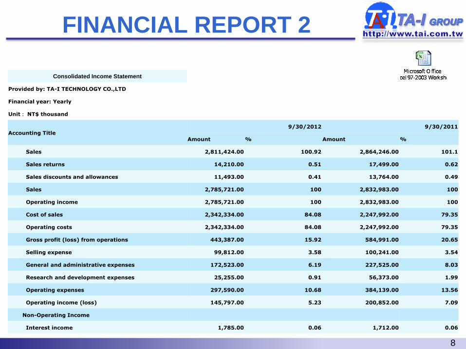
FINANCIAL REPORT 2
Consolidated Income Statement
Provided by: TA-I TECHNOLOGY CO.,LTD
Financial year: Yearly
Unit: NT$ thousand
Accounting Title9/30/2012 9/30/2011
Amount % Amount %
Sales 2,811,424.00 100.92 2,864,246.00 101.1
Sales returns 14,210.00 0.51 17,499.00 0.62
Sales discounts and allowances 11,493.00 0.41 13,764.00 0.49
Sales 2,785,721.00 100 2,832,983.00 100
Operating income 2,785,721.00 100 2,832,983.00 100
Cost of sales 2,342,334.00 84.08 2,247,992.00 79.35
Operating costs 2,342,334.00 84.08 2,247,992.00 79.35
Gross profit (loss) from operations 443,387.00 15.92 584,991.00 20.65
Selling expense 99,812.00 3.58 100,241.00 3.54
General and administrative expenses 172,523.00 6.19 227,525.00 8.03
Research and development expenses 25,255.00 0.91 56,373.00 1.99
Operating expenses 297,590.00 10.68 384,139.00 13.56
Operating income (loss) 145,797.00 5.23 200,852.00 7.09
Non-Operating Income
Interest income 1,785.00 0.06 1,712.00 0.06

9
2012 2013
Q3 Q4 Q1 Q2 Q3 Q4
Ultrathin package substrate
Electroless Ni/Ag Stability, Eutectic
Thickness< 0.25 mm
Laser marking Bad unit mark
E-map
Laser coding
High reflection COB
Traceability, record
High reflection
thermo stable material
System control for production
Flip chip eutectic substrateSmooth & flat surface
S/M thickness control
Thin film fill via holesMetal thickness < 0.02mm
Circuit Gap < 60um
Road Map

10
Core Technology
In-line Sputter
• In-line double sided
Sputter
No Particle Issue
Save process time
Save Pumping &
Venting times
• Over 10 Years Experience
Photolithograph
• Min. resolution 15 μm
•CCD Auto Alignment
Exposure
Max. Exposure Area:
6x6 inch2
Horizontal Tolerance
±10 μm
Increase Yield
• Over 10 Years Experience
Laser Drilling & Scribing
• Developed by TAI own tech.
Cost Down
With Various Function
• Min. Scribing Width 25μm
• Widely Choice Laser Type
Green / YAG / CO2
• Sufficient Production
Machine
Amount Above 150 sets
• Customized Drilling holes
position
• Customized Scribing
Pre-Cut
Post-Cut
• Over 20 Years Experience

11
Equipment investment plan in 2013 Unit : Set
2012.4 2013.2 2014.3
Laser Drilling (100W) 30 38 60
Laser Drilling (200W) 2 5 7
Sputter 1(7) 1(7) 2(8)
Photolithograph 5(8) 7(10) 13(16)
Cu Plating line 1(18) 1(18) 2(19)
AOI (Auto optical Inspect) 1 3 15
Silver Plating line 1 1 1
Total Capacity
(4.5” x 4.5”)250K (panels/M) 300K (panels/M) 500K (panels/M)
Package – CREE 207 165KKpcs/M 165KKpcs/M 275KKpcs/M
Equipment investment plan in 2013
Note : The number in () are the total equipments in whole TA-I group

12
*Cost
1.Equipment developed by TA-I
2.Bulk purchase the ceramic substrate that also applied in chip resistor
(Total quantity is 11KKpanel/M)
*Logistic
1.Adaptive and able to support by our factories located in Taiwan, China,
Malaysia and Indonesia.
Strength
1.Over 20 years experience in Thin film and Thick film technology that
applied to passive component and circuit protection component.
2.Higher production efficiency by equipment development with supplier

13
Production Process
Thin Film Process

14
New LED Factory
Current Size: 14,400 Square Feet
New Factory Size:115,200 Square Feet
Estimated Launch Date: Year 2014, Q1

15
Process of Thermal Dissipation Ceramic
-- Laser Stage
Laser
Scribing, Drilling
100W Fiber Laser
Ceramic
Via hole
16
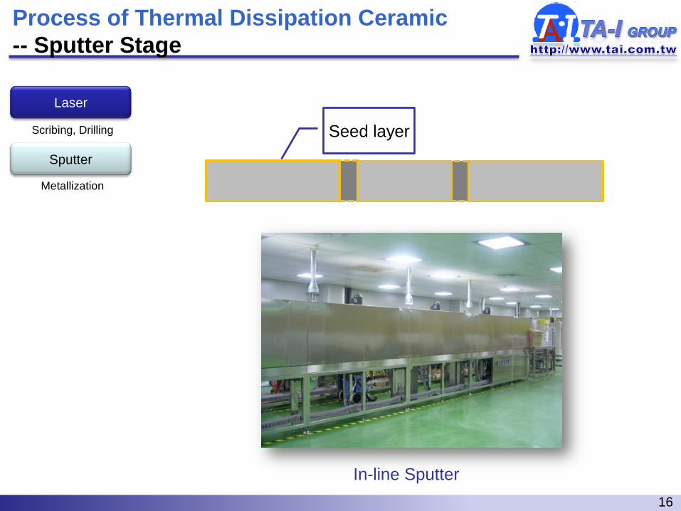
Laser
Sputter
Scribing, Drilling
Metallization
Process of Thermal Dissipation Ceramic
-- Sputter Stage
In-line Sputter
Seed layer

17
Laser
Sputter
Photolithograph
Scribing, Drilling
Metallization
Dry Film Wall
Process of Thermal Dissipation Ceramic
-- Photolithograph Stage
Auto Exposure DeveloperDry Film Lamination
Photo resistance
18
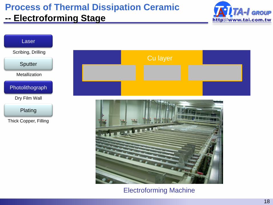
Laser
Sputter
Photolithograph
Plating
Scribing, Drilling
Metallization
Dry Film Wall
Thick Copper, Filling
Process of Thermal Dissipation Ceramic
-- Electroforming Stage
Electroforming Machine
Cu layer

19
Laser
Sputter
Photolithograph
Plating
Etching & Stripping
Scribing, Drilling
Metallization
Dry Film Wall
Thick Copper, Filling
Forming Circuit
Pattern
Process of Thermal Dissipation Ceramic
-- Etching & Stripping Stage
Etching Machine Stripping Machine Scrubbing Machine
Cu layer
Strip photo resistance
Etch seed layer
20
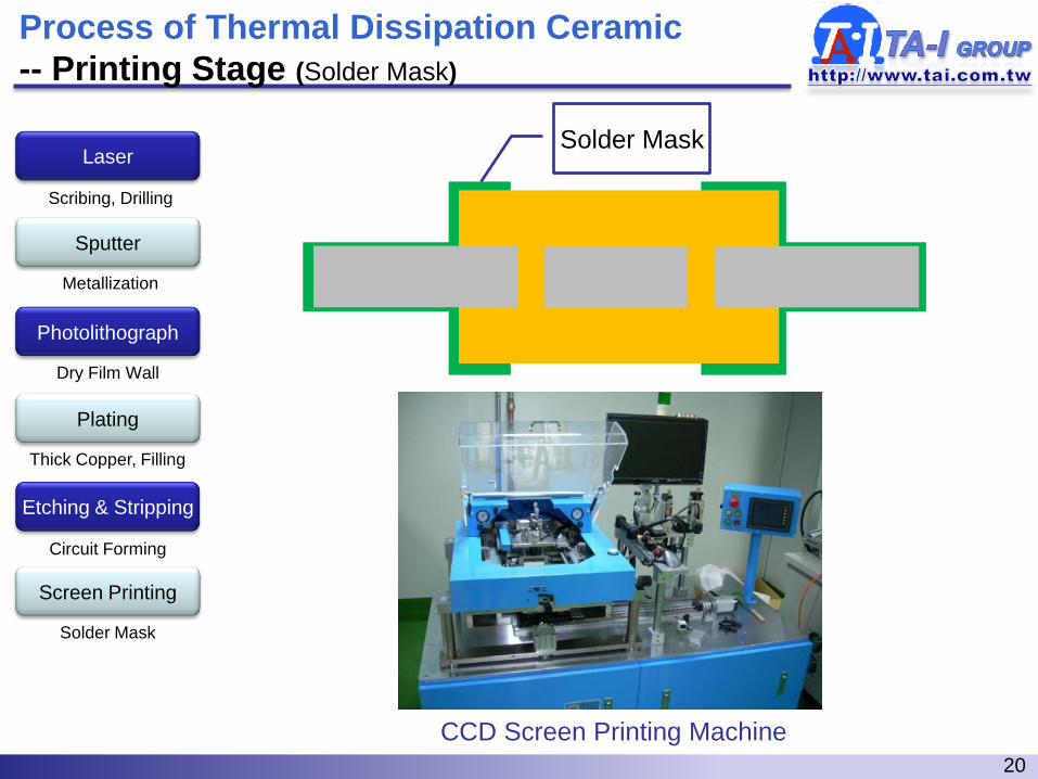
Laser
Sputter
Photolithograph
Plating
Etching & Stripping
Screen Printing
Scribing, Drilling
Metallization
Dry Film Wall
Thick Copper, Filling
Circuit Forming
Solder Mask
Process of Thermal Dissipation Ceramic
-- Printing Stage (Solder Mask)
CCD Screen Printing Machine
Solder Mask

21
Laser
Sputter
Photolithograph
Plating
Etching & Stripping
Screen Printing
Final Finish
Scribing, Drilling
Metallization
Dry Film Wall
Thick Copper, Filling
Circuit Forming
Solder Mask
Modify surface
Process of Thermal Dissipation Ceramic
-- Final Finish Stage
Chemical Ag Plating Machine
Type : NiPdAu / NiAg / NiAu / AgFinal finish
22
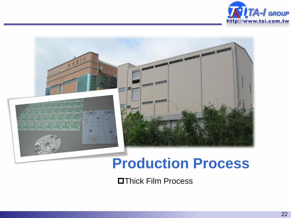
Production ProcessThick Film Process

23
Thick Film Process - Laser
Laser
100W fiber laser
Substrate

24
Thick Film Process - Screen Printing
Auto Screen Printer
Laser
Screen PrintingConductive Paste
Ag paste

25
Thick Film Process - Firing
Firing Furnace
Laser
Screen PrintingConductive Paste
Drying/FiringCircuit
Ag

26
Thick Film Process - Screen Printing
Auto Exposure
DeveloperCCD Screen Printing Machine
Laser
Screen PrintingConductive Paste
Drying/FiringCircuit
Screen PrintingSolder mask
S/M

27
Thick Film Process - Dispenser
Laser
Screen PrintingConductive Paste
Drying/FiringCircuit
Screen PrintingSolder mask
DispenserCavity Dispenser
Dispensing
Cavity

28
Specification-Heat dissipation substrate
Substrate Characteristics Metal Layer Characteristics
MaterialThickness
(mm)
Dimensions
(inch)
Thermal
Conductivity
(W/m.K)
Final Finish
Metal
Total
Thickness
(um)
Pattern
Construction
Resolution
(um)
Al2O3
Panel0.25/0.38/0.5/
0.635/1
4.5x4.5/4.75x4.75/
4.83x4.83
23-25
Cu-Ni-Au
Cu-Ni-Ag
Cu-Ni-Pd-Au
Cu-Ag
1-100
For
Customized
One sided
Two sided with
via holes
Customized
Min. 15
(Base on
thickness)
Al2O3
Chip0.25/0.38/0.5/
0.635/1Customized
AlN
Panel0.25/0.38/0.5/
0.635/1
4.5x4.5/4.75x4.75/
4.83x4.83
170-200
AlN
Chip0.25/0.38/0.5/
0.635/1Customized
29
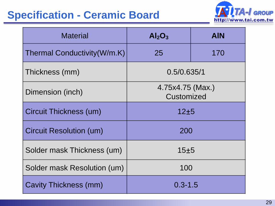
Specification - Ceramic Board
Material Al2O3 AlN
Thermal Conductivity(W/m.K) 25 170
Thickness (mm) 0.5/0.635/1
Dimension (inch)4.75x4.75 (Max.)
Customized
Circuit Thickness (um) 12±5
Circuit Resolution (um) 200
Solder mask Thickness (um) 15±5
Solder mask Resolution (um) 100
Cavity Thickness (mm) 0.3-1.5

30
Inspection Equipment
Flying probe machine
3D OM
Backlight OM
Electrical
Measurement AOI

31
Reliability Test
No. Item Parameter SpecificationReference
standard
1 Adhesion test
1. Temp. :RT
2. Tool:3M-610
3. Angle:180°
•The exterior must be no separate IPC-TM-650-2.4.1
2 Solderability
1. Temp.:235±5℃
2. Time:5±1sec
solder bath composition:
(Ag/Sn/Cu=3/96.5/ 0.5%)
•Coverage ≧90% ANSI/J-STD-003
3Thermal Stress
(IR Reflow)
1. Peak Temp.:260℃
2. Time: 10 second
3. Reflow Times:3 cycles
•The exterior must be no
separate, crack and warpage
•Maintain the electrical function
IPC-TM-650-2.6.27

32
Reliability Equipment
IR ReflowSurface Roughness
Meter (non-contact)
Push & Pull MeterWire Bonding Machine
Surface Roughness
Meter (contact)
Thermal Shock


34
HP/HB LEDs
• SMD LEDs - Chip Carrier
– Over 1 W Chip Carrier
– Dimension : customized
NiAu/NiPdAu-3535 (TA-I Pattern) Ag-3535 (TA-I Pattern)

35
Cavity on Substrate
Electroforming Solder Mask Dispensing Ceramic
•High resolution
•Low height
(<100um)
•Mass production•Complexity Process
•High resolution
•Low height
(<400um)
•Mass production
•Low resolution
•Wide: >250 um•Less manufacturing
Efficiency
•Low resolution
•High < 1000 um•Less Manufacturing
Efficiency

36
Reflectivity Solution
Increase surface reflection
Glossy surface substrate
(Smooth surface)Silver Plating
(High reflection metal)
Glossy Solder mask
(Reflectivity > 85%)

37
LED Lighting Module
AlN
Al2O3

38
Safety Standard
Dielectric Voltage Withstand
IEC/EN 60598
Basic insulation for voltages of SELV(a) 500
Basic insulation for voltages more than SELV(b) 2U+1000 (1440)
Supplementary insulation(c) 2U+1750 (2190)
Double or reinforced insulation(d) 4U+2750 (3630)
U=working voltage
UL 8750-2009
Between primary circuits or secondary circuits operation at greater than 70V peak and accessible dead conductive parts 2U+1000 (1440)
Between the primary and secondary of a transformer
U=working voltage

39
Lighting AC LED Board
Aluminum SubstrateThickness: 1.6 mm
Substituted
Disadvantages of Aluminum Substrate•Corrode
•Deformation•High Voltage
•Peeling
TA-I ceramic substrateThickness : 0.635/1 mm

40
Chip on Board (Al Substrate)
Chip on Board (Ceramic Substrate)
Street light COB module
Dispensing
Cavity
Low resolution
High limit (0.35-1.5 mm)
Suitable for COB
Sub.

41
BLU & Light Bar Application
0.3mm
90mm
5mm
Top View

42