table 1 summary of the measured performances of the …mirotzni/pdf/3d_simulations...3d simulations...
TRANSCRIPT

rejection. The micromixer consumes 15.6-mW power and occu-pies an area of only 660 � 420 �m, excluding the test pads.
ACKNOWLEDGMENTS
The support under grant no. NSC93-2212-E-260-003 is appreci-ated. The authors would like to thank the National NanometerDevice Laboratory for help with the high-frequency measure-ments.
REFERENCES
1. S. Chakraborty et al., Architectural trade-offs for SiGe BiCMOS directconversion receiver front-ends for IEEE802.11a, IEEE Gallium Ar-senide Integrated Circuit (GaAs IC) Symp 2002, pp. 120–123.
2. Y.K. Chu, C.H. Liao, and H.R. Chuang, 5.7-GHz 0.18-�m CMOSgain-controlled LNA and mixer for 802.11a WLAN applications,IEEE Radio Freq Integrated Circ (RFIC) Symp 2003, pp. 221–224.
3. B. Gilbert, The MICROMIXER: A highly linear variant of the Gilbertmixer using a bisymmetric Class-AB input stage, IEEE J Solid-StateCirc 32 (1997), 1412–1423.
4. T. Chouchane and M. Sawan, A 5-GHz CMOS RF mixer in 0.18-�mCMOS technology, IEEE CCECE 2003, pp. 1905–1908.
5. L.A. NacEachern and T. Manku, A charge-injection method for Gil-bert cell biasing, IEEE Canadian Conf Electrical Comp Eng, 1998, pp.365–368.
6. S. Liwei and L.E. Larson, An Si-SiGe BiCMOS direct-conversionmixer with second-order and third-order nonlinearity cancellation forWCDMA applications, IEEE Trans Microwave Theory Tech 51(2003), 2211–2220.
7. X. Li et al., A comparison of CMOS and SiGe LNA’s and mixers forwireless LAN application, IEEE Conf Custom Integrated Circ 2001,pp. 1905–1908.
8. J.B. Busquere et al., MEMS SiGe technologies for advanced wirelesscommunications, IEEE Radio Freq Integrated Circ Symp 2004, pp.247–250.
9. H.Y. Shih et al., A highly-integrated inductor-less SiGe W-CDMAtransmitter, IEEE Radio Frequency Integrated Circuits Symp, FortWorth, TX, 2004, pp. 439–442.
10. S. Wu and B. Razavi, A 900-MHz/1.8-GHz CMOS receiver fordual-band applications, IEEE J Solid-State Circ 33 (1998), 2178–2185.
11. H. Koizumi et al., A GaAs single balanced mixer MMIC with built-inactive balun for personal communication systems, IEEE MicrowaveMillimeter-Wave Monolithic Circ Symp, Orlando, FL, 1995.
12. B. Razavi, RF microelectronics, Prentice Hall, New Jersey, 1998.
© 2005 Wiley Periodicals, Inc.
3D SIMULATIONS OF ELECTRICALLYLARGE THIN PLATES USING THEHYBRID PSTD-FDTD ALGORITHM
Xiang Gao,1 Mark S. Mirotznik,2 Shouyuan Shi,3 andDennis W. Prather3
1 160 Rio Robles, MS A-2026San Jose, CA 951342 Department of Electrical Engineering and Computer ScienceThe Catholic University of AmericaWashington, DC 200643 Department of Electrical & Computer EngineeringUniversity of DelawareNewark, DE 19716
Received 10 December 2004
ABSTRACT: Many optical and electromagnetic applications involvelarge thin plates, which include planar waveguides, diffractive opticalelements, photo masks, filters, and so forth. Typically, those structureshave a relatively small thickness and a very large surface. Three-dimen-sional (3D) simulation of those thin plates using FDTD, which requiresa large sampling rate, is sometimes unpractical due to the memory re-quirement. In this paper, we investigate 3D simulations of electricallylarge thin plates using the hybrid PSTD-FDTD method. As an example,we study the near-field scattering of a photo mask and compare the hy-brid method with the FDTD method. © 2005 Wiley Periodicals, Inc.Microwave Opt Technol Lett 45: 502–507, 2005; Published online inWiley InterScience (www.interscience.wiley.com). DOI 10.1002/mop.20864
Key words: FDTD; PSTD; Liao’s ABC; photo mask; planarwaveguide; diffractive optical element
1. INTRODUCTION
Many optical and electromagnetic (EM) applications involve thinplates whose effective region is very thin in the vertical directionand very large in the horizontal directions. Examples include, butare not limited to: planar waveguides used in integrated optics,diffractive elements (lenses, gratings, and so forth) fabricated onflat dielectric substrates, computer-generated holograms, andphoto masks used in photolithography. We call these structuresoptical plates, EM plates, or simply thin plates. Sometimes a 3Dsimulation based on vector theory is required for designing thosethin plates. However, time-domain techniques, such as FDTD,typically require a large sampling rate (�12 grids per minimumwavelength) in order to ensure reasonable accuracy. Hence, FDTDis only applicable to thin plates with a small area.
Recently, the Fourier pseudospectral time-domain (PSTD) al-gorithm [1–14] was developed to study low-contrast dielectricmaterials. Unlike the FDTD algorithm, which uses central differ-ence to calculate spatial derivatives, Fourier PSTD obtains thespatial derivatives analytically in the spectral domain so that itssampling-rate requirement is only slightly larger than the Nyquistsampling rate. This translates into tremendous memory savings(�4D, with D the dimensionality) for 2D and 3D problems [1]. Arecent finding of some dispersion compensation techniques alsoadds another advantage of the PSTD algorithm [13], that is,smaller numerical-dispersion errors.
However, there are some difficulties with the Fourier PSTDalgorithm, such as [1, 11]: (i) soft source generation, (ii) high-contrast materials, and (iii) fine structures, and so on. The softsource-generation problem can be avoided by using the scattered-
This work was completed while the first author was at the ECE Depart-ment, University of Delaware.
TABLE 1 Summary of the Measured Performances of theSiGe Micro-Mixer
fRF � 5.2 GHz, fLO � 4.9 GHz, and fIF � 300 MHz (P1dB � 0 dBm)
Supply voltage 3 VCurrent consumption of the mixer core 5.2 mARF power �35 dBmLO power 3 dBmConversion gain 7.3 dBLO-to-IF isolation 45 dBLO-to-RF isolation 50 dBRF-to-IF isolation 28.5 dBIIP3 0.5 dBm
502 MICROWAVE AND OPTICAL TECHNOLOGY LETTERS / Vol. 45, No. 6, June 20 2005

field formulation or can be solved by using the recently developedweighted total-field/scattered-field (TF/SF) approach [11]. Prob-lems (ii) and (iii) are tricky, since the resolution may require afundamental change in the Fourier PSTD scheme. In high-contrastmaterials, the solution itself or its derivatives are not continuous,which makes it questionable to use Fourier series as basis func-tions. The common solution to problem (ii) is to use the Chebyshevpolynomials and Gauss–Lobatto collocation points. This yields themultidomain PSTD algorithm [15–17], which separates the com-putation domain along material boundaries into smaller subdo-mains, each of which is a uniform medium. Then a collocation(pseudospectral) algorithm is applied in each subdomain, withoutbeing affected by the Gibbs phenomenon. To connect the neigh-boring subdomains, a domain-patching condition is applied to thesubdomain boundaries. In addition to the multidomain PSTD ap-proach, if the material geometry is rectangular, one can use theso-called mapped PSTD [12, 14] to reduce the singularity of thesolution in a mapped space, and safely apply the Fourier PSTDalgorithm. This method is shown to be accurate and efficient andonly requires some minor changes to existing Fourier PSTD pro-grams. By introducing a nonuniform grid that aligns with materialboundaries as in the mapped PSTD [12], or a conformal grid as inmultidomain PSTD, the small-feature problem can be accuratelyhandled as well. However, more case studies are needed to furtherprove their flexibility and accuracy.
Recently, Leung and Chan suggested a combination of PSTDand FDTD method applied in different directions [5]. It wassuggested that FDTD be applied to directions along which thematerial is highly nonhomogeneous and has fine structures and thatPSTD be applied in directions along which the material propertycontrast is small and the structures are relatively large. In thispaper, we apply this concept in 3D simulations of thin-plateproblems. We use FDTD in the z direction, which is perpendicularto the thin plate surface and PSTD in the x and y directions. Thereare several advantages in so doing. First, normal incident wavescan be introduced easily by applying the TF/SF technique in the zdirection. Otherwise, if we apply PSTD in the z direction, either ascattered-field formation or the weighted TF/SF formulation willneed to be used [11]. Neither of them is as efficient and simple asthe TF/SF formulation in FDTD. Second, from the computation-efficiency point of view, because the vertical dimension of thecomputation region is very small, it is more efficient to use FDTDthan PSTD in the z direction. This is because the number ofnumerical operations in the FFT algorithm (N log N) is lessadvantageous when N is small [18, 19]. Third, for thin-plateproblems, thin films are usually used on the surface. This producesvery fine structures in the z direction, and the dense grid of FDTDis very suitable for those fine structures. Fourth, the size of thecomputation region in the x and y directions is very large and thestructures are relatively large in these directions. Applying PSTDin the x and y directions can save both memory and computationtime [1, 12].
2. A HYBRID PSTD-FDTD ALGORITHM
In the hybrid PSTD-FDTD algorithm, we apply finite difference inthe z direction and Fourier pseudospectral method in the x and ydirections. In implementation, we simply stagger E and H grids inthe z direction and use unstaggered grid in the x and y directions.Figure 1 shows the arrangement of the E and H grids in space.
In the time domain, the E and H grids are interleaved, and aleapfrog scheme is applied in time marching, the same as FDTDand Fourier PSTD. Thus, in a Cartesian coordinate, the Maxwell’scurl equations can be written as the following difference equations,
after using the transformation for the H fields, Hnew � Z0Hold
[20]:
Hxn�1/ 2 � DaHx
n�1/ 2 � Db� �
� yEz
n ��
� zEy
n� , (1a)
Hyn�1/ 2 � DaHy
n�1/ 2 � Db� �
� zEx
n ��
� xEz
n� , (1b)
Hzn�1/ 2 � DaHz
n�1/ 2 � Db� �
� xEy
n ��
� yEx
n� , (1c)
Exn�1 � CaEx
n � Cb� �
� yHz
n�1/ 2 ��
� zHy
n�1/ 2� , (1d)
Eyn�1 � CaEy
n � Cb� �
� zHx
n�1/ 2 ��
� xHz
n�1/ 2� , (1e)
Ezn�1 � CaEz
n � Cb� �
� xHy
n�1/ 2 ��
� yHx
n�1/ 2� . (1f)
In Eqs. (1a)–(1f) the constants Ca, Cb, Da, and Db are defined asfollows:
Ca �2�r�0 � ��t
2�r�0 � ��t, (2a)
Cb �2�0c0�t
2�r�0 � ��t, (2b)
Da �2�r�0 � �*�t
2�r�0 � �*�t, (2c)
Db ��2�0c0�t
2�r�0 � �*�t. (2d)
Figure 1 Diagram of the E and H grids in space. [Color figure can beviewed in the online issue, which is available at www.interscience.wiley.com.]
MICROWAVE AND OPTICAL TECHNOLOGY LETTERS / Vol. 45, No. 6, June 20 2005 503

We assume the E grid is located at z � K�z, K � 0, 1,2, . . . , and the H grid is located at z � (K � 1/ 2)�z. Becausethe update of E fields requires H fields at the same z location, andvice versa, we use the average value of H or E fields fromneighboring grids in the z direction. To see that, we use E� �x,y,K
n torepresent the E-field component at ( x, y, K�z) and t � n�t,then E� �x,y,K�1/ 2
n � (E� �x,y,K�1n � E� �x,y,K
n )/ 2, and H� �x,y,Kn�1/ 2 �
(H� �x,y,K�1/ 2n�1/ 2 � H� �x,y,K�1/ 2
n�1/ 2 )/ 2. Now, we look at the Eq. (1a),which can be written as
Hx�x,y,K�1/ 2n�1/ 2 � DaHx�x,y,K�1/ 2
n�1/ 2 � Db� �
� yEz�x,y,K�1/ 2
n ��
� zEy�x,y,K�1/ 2
n � .
(3)
In Eq. (3), the spatial derivatives in the z direction are carried outvia central difference as follows:
�
� zEy�x,y,K�1/ 2
n � �Ey�x,y,K�1n � Ey�x,y,K
n /�z, (4)
Figure 2 Diagram of the mask structure and computation region. [Colorfigure can be viewed in the online issue, which is available at www.interscience.wiley.com.]
Figure 3 Dimensions of the mask pattern used for the numerical exper-iments in section 3
Figure 4 (a) Steady-state total E field at z � 195 nm obtained from thehybrid 3D calculation described in the text (the absorbing material has � �1 � 104 S/m and skin depth � � 0.53 �m); (b) corresponding steady-stateE field obtained from the FDTD calculation described in the text. [Colorfigure can be viewed in the online issue, which is available at www.interscience.wiley.com.]
504 MICROWAVE AND OPTICAL TECHNOLOGY LETTERS / Vol. 45, No. 6, June 20 2005
and the derivative �/� y is carried out through the FFT/iFFTalgorithm used in Fourier PSTD [1, 11, 13]:
�
� yEz�x,y,K�1/ 2
n ��
� y�Ez�x,y,K
n � Ez�x,y,K�1n / 2
� iFFTikyFFT��Ez�x,y,Kn � Ez�x,y,K�1
n /2� . (5)
The derivatives for the rest of the difference equations in Eqs.(1a)–(1f) can be obtained similarly.
This hybrid PSTD-FDTD algorithm has the following disper-sion relationship [5]:
4
�c�t2 sin2��t
2 � � kx2 � ky
2 � � 2
�z�2
sin2�kz�z
2 �, (6)
and the following stability criterion [5]:
�t 2
c�� �
�x�2
� � �
�y�2
� � 2
�z�2 . (7)
3. NUMERICAL RESULTS
We simulated the plane-wave normal incidence on a photo maskusing the hybrid PSTD-FDTD method and the FDTD method. Themask substrate is glass and has a 100-nm-thick absorbing layerformed on its surface. The structure is shown in Figure 2, wherethe computation region is indicated by the dashed-line box, withdimensions Lx, Ly, and Lz. The glass substrate is assumed to besemi-infinite. A polarized plane-wave soft source is launched
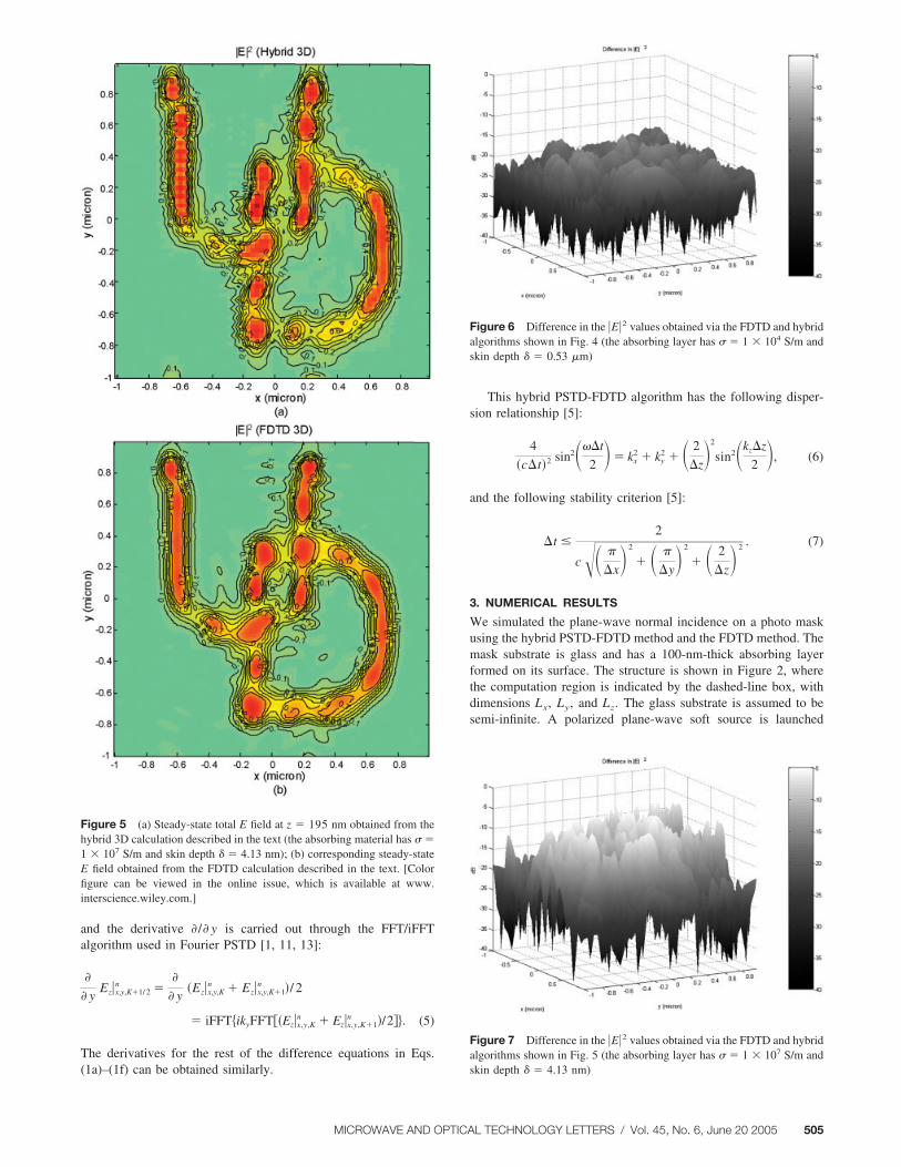
Figure 5 (a) Steady-state total E field at z � 195 nm obtained from thehybrid 3D calculation described in the text (the absorbing material has � �1 � 107 S/m and skin depth � � 4.13 nm); (b) corresponding steady-stateE field obtained from the FDTD calculation described in the text. [Colorfigure can be viewed in the online issue, which is available at www.interscience.wiley.com.]
Figure 6 Difference in the �E�2 values obtained via the FDTD and hybridalgorithms shown in Fig. 4 (the absorbing layer has � � 1 � 104 S/m andskin depth � � 0.53 �m)
Figure 7 Difference in the �E�2 values obtained via the FDTD and hybridalgorithms shown in Fig. 5 (the absorbing layer has � � 1 � 107 S/m andskin depth � � 4.13 nm)
MICROWAVE AND OPTICAL TECHNOLOGY LETTERS / Vol. 45, No. 6, June 20 2005 505

towards the �z direction inside the glass. The soft source isintroduced by simply using the TF/SF formulation. This is consis-tent with the semi-infinite assumption of the substrate. The steady-state field behind the absorbing layer is the field of interest.
Second-order Liao’s absorptive boundary conditions (ABCs)are applied in the z direction and periodical boundary conditions(PBCs) are assumed in the x and y directions. In general, if themask patterns are not periodic in the x and y directions, one cansimply leave enough “blank space” near the computation boundaryin the x and y directions, without being affected by the PBC. Thisis because the affected regions due to the PBCs are not large whenLz is very small.
As an example, we studied a small area of a photo mask, withLx � Ly � 2.0 �m and Lz � 0.2 �m. The mask pattern is shownin Figure 3, where the dark region corresponds to air. A normalincident plane wave, as shown in Figure 2, is polarized in the ydirection with amplitude of 1 and wavelength of 200 nm. Theincident wave front is smoothed by a raised-cosine envelopefunction in order to reduce nonphysical transient effects. For thecomputation region, we use a grid size of Nx � 70, Ny � 70, andNz � 40. As a result, �x � �y � 28.57 nm and �z � 5 nm. Thisis equivalent to 4.67 grids per minimum wavelength in the x andy directions and 26.67 grids per minimum wavelength in the zdirection. The glass/absorbing layer interface is located at z � 25nm and the detector plane is located at z � 195 nm. We experi-mented with two artificial absorbing materials. Material 1 has �r �1, �r � 1, �* � 0 S/m, and � � 1 � 104 S/m. Material 2 has�r � 1, �r � 1, �* � 0 S/m, and � � 1 � 107 S/m. For the200-nm wavelength, material 1 has a reflection coefficient � �0.0299 and a skin depth � � 0.53 �m. As a result, the Gibbsphenomenon due the discontinuous material property is very small.Material 2 has � � 0.8787 and a very small skin depth � � 4.13nm, so the solution should show a strong Gibbs phenomenon. Thetotal fields at the detector plane, which is 70-nm behind theabsorbing layer, are obtained from calculations with the aforemen-tioned parameters, and the total E fields on the detector plane areshown in Figures 4(a) and 5(a).
To verify our algorithm, we also studied the same structurewith the same source using the FDTD algorithm, which also usesthe same boundary conditions as the hybrid method. In compari-son, the FDTD method uses a grid of Nx � 400, Ny � 400, andNz � 40, with an average sampling rate of 26.67 grids perminimum wavelength in all directions. The steady state total E
fields are shown in Figures 4(b) and 5(b). The difference of �Etot�2
between these two methods are shown in Figures 6 and 7, wherethe “dB” for the z-axis is defined as 10 log10(��Etot�
2). As can beseen in Figure 6, if the solution is smooth, that is, with little Gibbsphenomenon, PSTD is able to achieve results that are very close tothose of FDTD, yet with much smaller memory usage. In thisexample, there is a memory saving of about 32. To compare thecomputation speeds, we ran simulations on a PC with 1-Gbsmemory and one 1.8-GHz CPU. To conduct a fair comparison,both the FDTD and Hybrid codes were optimized and written inMatlab. In this example, the FDTD simulation ran on virtualmemory and took more than 12 h to finish, while the PSTDsimulation did not use virtual memory and took less than 16 min(see Table 1). To get a better idea of the computation speedup, wealso ran simulations with smaller grid sizes to avoid using virtualmemory in our PC. Table 2 shows that the hybrid algorithm wasable to achieve a speedup larger than 13. For an analysis of thecomputation complexity of FDTD and PSTD, please refer to[1, 12].
4. DISCUSSION
In our numerical codes used in section 3, we applied the 2nd-orderLiao’s ABCs [21–24] in the z direction. Liao’s ABC is mosteffective when the boundary has a uniform propagation speed.However, in our model there are two materials on the boundariesof the computation domain. The top layers (near z � 0) are glassand the bottom layers (near z � Lz) are air. So the Liao’s ABCsare different for the bottom and top boundaries. If the same Liao’sformula is applied to both boundaries, interpolation needs to beused. In our numerical experiments, however, we found that Liao’sABC has problems with stability and absorption if interpolation isused. To avoid using interpolation, we use multiple time steps.Specifically, we use the following formulas for the grid boundary:
Un�1�Ib � 2Un�1�Ib � 1 � Un�3�Ib � 2, (8)
and
Un�1�Ib � 2Un�2�Ib � 1 � Un�5�Ib � 2. (9)
Following the naming in [23], we call Eq. (8) a 2nd-order Liao’s T2ABC, and Eq. (9) a 2nd-order Liao’s T3 ABC. The time step is
TABLE 1 Summary for Computation
MethodGrid Size
[Nx � Ny � Nz]
Average Sampling Rate[grid per minimum
wavelength] �t [s]Number of Total
Time StepsTotal Computation
Time [min]
FDTD 400 � 400 � 40 26.7 8.339 � 10�18 360 760*Hybrid 70 � 70 � 40 4.67 in x- and y-axis;
26.7 in z-axis8.339 � 10�18 360 15.5
* running on virtual memory.
TABLE 2 Summary for Computation
MethodGrid Size
[Nx � Ny � Nz]
Average Sampling Rate[grid per minimum
wavelength] �t [s]Number of Total
Time StepsTotal Computation
Time* [min]
FDTD 200 � 200 � 20 13.33 1.668 � 10�17 180 12.58Hybrid 35 � 35 � 20 2.33 in x- and y-axis;
13.33 in z-axis1.668 � 10�17 180 0.87
* without using virtual memory.
506 MICROWAVE AND OPTICAL TECHNOLOGY LETTERS / Vol. 45, No. 6, June 20 2005

fixed as �t � 0.5�z/c. Then the 2nd-order Liao’s T2 ABC isapplied in the lower boundary where the material is air and the2nd-order Liao’s T3 ABC is applied in the upper boundary wherethe material is glass, with a refractive index of 1.5.
The stability criterion for the hybrid algorithm is given by Eq.(7), but Liao’s ABC requires �t � 0.5�z/c. In general, if weassume �x � �y, then we can obtain the following stabilitycriterion for using Liao’s ABC:
�x � �y ���z
�6� 1.283�z. (10)
This is generally satisfied since, in the x and y directions, a lowersampling rate is usually used to take the advantage of the PSTDalgorithm.
Because we use Fourier PSTD with a uniform grid in the x andy directions, the hybrid algorithm in this paper requires that thematerial contrast in the x and y directions is not too large. Other-wise, the severe Gibbs phenomenon will contaminate the simula-tion results. In our numerical experiments, we found that whenskin depth of the absorbing layer is very small, in which the caseGibbs phenomenon is sure to appear, there are fairly large differ-ences in the field values obtained via the hybrid method and thoseobtained via FDTD with smaller grid size (see Fig. 7). Here wepropose several possible remedies for high-contrast materials andgood conductors, if they are included in the computation domain:(i) If the object geometry is rectangular on the mask surface, wecan use the mapped PSTD along the x and y directions to helpreduce the magnitude of the Gibbs phenomenon in the mappedspace [12, 14]; (ii) if the object geometry is not rectangular but canbe handled with multidomain PSTD, we suggest using multido-main PSTD in the x and y directions; (iii) use regular FourierPSTD for the x and y directions and then apply a low-pass filter tothe final steady-state results contaminated by the Gibbs phenom-enon. This may help restore the global exponential convergenceproperty of the PSTD algorithm. We expect to see more progressin these areas in the near future.
5. CONCLUSION
In this paper, we have applied a hybrid PSTD-FDTD algorithm forelectrically large thin-plate problems. We adopted FDTD along thevertical direction of the thin plate and PSTD along the horizontaldirections. This arrangement can combine the advantages of boththe FDTD and PSTD algorithms. As an example application, westudied the near-field scattering of a photo mask, and the hybridalgorithm was shown to offer large savings in memory usage andcomputation time, as compared with the FDTD method.
REFERENCES
1. Q.H. Liu, The PSTD algorithm: A time-domain method requiring onlytwo cells per wavelength, Microwave Opt Technol Lett 15 (1997),158–165.
2. Q.H. Liu, PML and PSTD algorithm for arbitrary lossy anisotropicmedia, IEEE Microwave Guided Wave Lett 9 (1999), 48–50.
3. Q.H. Liu, A frequency-dependent PSTD algorithm for general disper-sive media, IEEE Microwave Guided Wave Lett 9 (1999), 51–53.
4. Q.H. Liu, Large-scale simulations of electromagnetic and acousticmeasurements using the pseudospectral time-domain (PSTD) algo-rithm, IEEE Trans Geosci Remote Sensing 37 (1999), 917–926.
5. Y.F. Leung and C.H. Chan, Combining the FDTD and PSTD methods,Microwave Opt Technol Lett 23 (1999), 249–254.
6. Q. Li, Y. Chen, and C.K. Li, Hybrid PSTD-FDTD technique forscattering analysis, Microwave Opt Technol Lett 34 (2002), 19–24.
7. Y.F. Leung and C.H. Chan, Pseudospectral time-domain (PSTD)
method with unsplit-field PML, Microwave Opt Technol Lett 22(1999), 278–283.
8. Q.L. Li, Y.C. Chen, and D. Ge, Comparison study of the PSTD andFDTD methods for scattering analysis, Microwave Opt Technol Lett25 (2000), 220–226.
9. G.X. Fan and Q.H. Liu, Pseudospectral time-domain algorithm appliedto electromagnetic scattering from electrically large objects, Micro-wave Opt Technol Lett 29 (2001), 123–125.
10. Q.H. Liu and J.Q. He, An efficient PSTD algorithm for cylindricalcoordinates, IEEE Trans Antennas Propagat 49 (2001), 1349–1351.
11. X. Gao, M.S. Mirotznik, and D.W. Prather, A method for introducingsoft sources in the PSTD algorithm, IEEE Trans Antennas Propagat 52(2004), 1665–1971.
12. X. Gao, M.S. Mirotznik, S. Shi, and D.W. Prather, Applying a mappedpseudospectral time-domain method in simulating diffractive opticalelements, J Optics Soc Am A 21 (2004), 777–785.
13. X. Gao, M.S. Mirotznik, and D.W. Prather, Dispersion compensationtechniques for the PSTD algorithm, Microwave Opt Technol Lett 42(2004), 357–361.
14. X. Gao, M.S. Mirotznik, and D.W. Prather, Simulation of metallicmaterials with mapped Fourier PSTD algorithm, Microwave OptTechnol Lett (to appear).
15. B. Yang, D. Gottlieb, and J.S. Hesthaven, Spectral simulations ofelectromagnetic wave scattering, J Computat Phys 134 (1997), 216–230.
16. B. Yang and J.S. Hesthaven, Multidomain pseudospectral computationof Maxwell’s equations in 3D general curvilinear coordinates, ApplNumer Mathem 33 (2000), 281–289.
17. G.X. Fan, Q.H. Liu, and J.S. Hesthaven, Multidomain pseudospectraltime-domain simulations of scattering by objects buried in lossy me-dia, IEEE Trans Geosci Remote Sensing 40 (2002), 1366–1373.
18. J.W. Cooley and J.W. Tukey, Algorithm for the machine computationof complex Fourier series, Math Comput 19 (1965), 2977–301.
19. R.N. Bracewell, The Fourier transform and its applications, 2nd ed.,McGraw-Hill, New York, 1986.
20. A. Taflove and S.C. Hagness, Computational electrodynamics: Thefinite-difference time-domain method, 2nd ed., Artech House, Boston,
21. Z.P. Liao, H.L. Wong, B.P. Yang, and Y.F. Yuan, A transmittingboundary for transient wave analyses, Scientia Sinica A 27 (1984),1063–1076.
22. Z.P. Liao, Extrapolation nonreflecting boundary conditions, WaveMotion 24 (1996), 117–138.
23. P. Yang and K.N. Liou, An efficient algorithm for truncating spatialdomain in modeling light scattering by FDTD technique, J ComputatPhys 140 (1998), 346–369.
24. P. Yang and K.N. Liou, Light scattering by hexagonal ice crystals:Comparison of finite-difference time domain and geometric opticsmodels, J Optics Soc Am A 12 (1995), 162–176.
© 2005 Wiley Periodicals, Inc.
MODELLING OF THE CMOS BURIEDDOUBLE-JUNCTION PHOTODETECTOR
S. Feruglio, V. Fouad Hanna, G. Alquie, and G. VasilescuLISIF, University Pierre & Marie Curie3, rue Galilee, Site Raphael94200 Ivry sur Seine, France
Received 8 December 2004
ABSTRACT: In this paper, a general model of the buried double-junc-tion (BDJ) photodetector is proposed for DC, AC, and noise analysis. Inconjunction with the analytical expressions of photo-generated and darkcurrents, this model can be applied to all BDJ operating modes. More-over, it can be easily extended to any multilayer PN junction device.The experimental results obtained for various devices realized using the0.35-�m CMOS technology show good agreement with the simulation
MICROWAVE AND OPTICAL TECHNOLOGY LETTERS / Vol. 45, No. 6, June 20 2005 507