tandem, triple and quadruple junction polymer solar cells · 1.2 organic solar cells organic solar...
TRANSCRIPT

Tandem, triple and quadruple junction polymer solar cells
Citation for published version (APA):Di Carlo Rasi, D. (2018). Tandem, triple and quadruple junction polymer solar cells. Eindhoven: TechnischeUniversiteit Eindhoven.
Document status and date:Published: 10/12/2018
Document Version:Publisher’s PDF, also known as Version of Record (includes final page, issue and volume numbers)
Please check the document version of this publication:
• A submitted manuscript is the version of the article upon submission and before peer-review. There can beimportant differences between the submitted version and the official published version of record. Peopleinterested in the research are advised to contact the author for the final version of the publication, or visit theDOI to the publisher's website.• The final author version and the galley proof are versions of the publication after peer review.• The final published version features the final layout of the paper including the volume, issue and pagenumbers.Link to publication
General rightsCopyright and moral rights for the publications made accessible in the public portal are retained by the authors and/or other copyright ownersand it is a condition of accessing publications that users recognise and abide by the legal requirements associated with these rights.
• Users may download and print one copy of any publication from the public portal for the purpose of private study or research. • You may not further distribute the material or use it for any profit-making activity or commercial gain • You may freely distribute the URL identifying the publication in the public portal.
If the publication is distributed under the terms of Article 25fa of the Dutch Copyright Act, indicated by the “Taverne” license above, pleasefollow below link for the End User Agreement:www.tue.nl/taverne
Take down policyIf you believe that this document breaches copyright please contact us at:[email protected] details and we will investigate your claim.
Download date: 29. May. 2020

Tandem, Triple, and Quadruple Junction Polymer Solar
Cells
PROEFSCHRIFT
ter verkrijging van de graad van doctor aan de Technische Universiteit Eindhoven,
op gezag van de rector magnificus prof.dr.ir. F.P.T. Baaijens,
voor een commissie aangewezen door het College voor Promoties, in het openbaar
te verdedigen op maandag 10 december 2018 om 13:30 uur
door
Dario Di Carlo Rasi
geboren te Frascati, Italië

Dit proefschrift is goedgekeurd door de promotoren en de samenstelling van de
promotiecommissie is als volgt:
voorzitter: prof.dr.ir. E.J.M. Hensen
1e promotor: prof.dr.ir. R.A.J. Janssen
copromotor: dr.ir. M.M. Wienk
leden: prof.dr. K. Vandewal (Universiteit Hasselt)
prof.dr. J. Martorell (ICFO)
prof.dr.ir. W.M.M. Kessels
prof.dr. L.J.A. Koster (RUG)
dr. S.C.J. Meskers
Het onderzoek of ontwerp dat in dit proefschrift wordt beschreven is uitgevoerd in
overeenstemming met de TU/e Gedragscode Wetenschapsbeoefening.

Printed by: Gildeprint
A catalogue record is available from the Eindhoven University of Technology Library
ISBN: 978-90-386-4642-8.
The research described in thesis has been financially supported by the European
Community’s Seventh Framework Programme in the ITN project OSNIRO (No. 607585),
the European Research Council (Advanced, Grant (No. 339031), and the Ministry of
Education, Culture and Science (Gravity Program No. 024.001.035).

Table of Contents
Chapter 1: Introduction 1
1.1 Solar cells 2
1.2 Organic solar cells 3
1.3 Characterization of solar cells 5
1.4 Multi-junction organic solar cells 7
1.4.1 Working principles 7
1.4.2 Early developments 8
1.4.3 Characterization of multi-junction organic solar cells 11
1.4.4 Determination of the wavelength-dependent n and k optical constants 12
1.5 Aim and outline of the thesis 13
1.6 References 15
Chapter 2: Recent Developments on Solution-Processed Multi-Junction Organic
Solar Cells
19
2.1 Introduction 20
2.2 Tandem solar cells 21
2.2.1 ICL materials 21
2.2.2 Processing multi-junction stacks 25
2.2.3 Light management 28
2.2.4 Active layer materials 31
2.2.5 Upscaling 42
2.3 Three- and four-fold junction solar cells 49
2.4 Accurate characterization 52
2.5 Unusual device architectures 56
2.6 Use of multi-junction polymer solar cells for photoelectrochemical water
splitting
57
2.7 Conclusions 59
2.8 References 61

Chapter 1
Chapter 3: A Universal Route to Fabricate n-i-p Multi-Junction Polymer Solar
Cells via Solution Processing
67
3.1 Introduction 68
3.2 Results and Discussion 69
3.2.1 Materials and device architectures 69
3.2.2 PEDOT:PSS as HTL 73
3.2.3 PEIE and ZnO nanoparticles as ETL 76
3.2.4 Tandem solar cells 77
3.2.5 ICL for triple-junction solar cells: need for second order orthogonality 79
3.2.6 Triple-junction solar cells 81
3.2.7 Synopsis 85
3.3 Conclusions 85
3.4 Experimental Section 86
3.5 References 91
Chapter 4: Accurate Characterization of Triple-Junction Polymer Solar Cells 95
4.1 Introduction 96
4.2 Results and Discussion 97
4.2.1 The design of the triple-junction cell 97
4.2.2 Measuring the performance under simulated AM1.5G light 99
4.2.3 EQE of the triple junction using bias light 100
4.2.4 Corrections to the EQE measurement 102
4.2.5 Reconstructing the J−V-curve 105
4.3 Conclusions 108
4.4 Experimental Section 109
4.5 References 113
Chapter 5: Quadruple-Junction Polymer Solar Cells with Four Complementary
Absorber Layers
115
5.1 Introduction 116
5.2 Results and discussion 117
5.2.1 Layers stack and optimization 117
5.2.2 Performance of the quadruple-junction solar cell 121
5.3 Conclusions 126
5.4 Experimental Section 126
5.5 References 130

Introduction
Chapter 6: Solution-Processed Tin Oxide-PEDOT:PSS Interconnecting Layers
for Efficient Inverted and Conventional Tandem Polymer Solar Cells
131
6.1 Introduction 132
6.2 Results and Discussion 133
6.2.1 Single-junction Cells with SnO2 Charge Transport Layers 133
6.2.2 Tandem Solar Cells with SnO2 and PEDOT:PSS Interconnecting Layer 134
6.2.3 Advantage of SnO2 over ZnO 141
6.3 Conclusions 142
6.4 Experimental Section 143
6.5 References 148
Summary 149
Biography 153
List of Publications and Contributions 155
Acknowledgements 159
Appendix 163


Chapter 1
Introduction*
Abstract
This Chapter starts with a brief history of solar cells and describes the current status
of existing photovoltaic technologies. Further, the basic principles of organic solar cells are
outlined, referring to the first seminal studies on these devices. Important device metrics for
solar cells are introduced and the characterization methods to determine these are described.
With these notions laid down, the topic of the thesis, multi-junction organic solar cells, is
introduced with explaining the working mechanism, the principal advantages and providing
a short historical description of early developments on these devices. Next, the aim and
outline of the thesis is presented.
* Part of this chapter has been included in an article, submitted for publication as: D. Di
Carlo Rasi, R. A. J. Janssen. Advances in Solution-Processed Multi-Junction Organic Solar
Cells.

Chapter 1
2
1.1 Solar cells
The world’s population increases steadily, counting around 7.7 billion people
nowadays and is expected to further grow to 9.8 billion around 2050.[1] This growth implies
a high future demand for energy. Global energy is currently mainly provided by tapping from
traditional sources based on fossil fuels. Intrinsic to the consumption of fossil fuels is the
production of carbon dioxide. Consequently, carbon dioxide concentrations in the earth
atmosphere are now over 400 ppm and progressively raise the global temperature, known as
the greenhouse effect. To mitigate the threat of climate change it is of great urgency to exploit
alternative energy sources. Solar energy reaching the surface of the earth can comply with
the current and future energy demand,[2] while preserving the quality of the environment. The
conversion of solar light into electricity was first observed by Bequerel in the 19th century,[3]
but the development of crystalline silicon p-n junction solar cells in 1954 by Chapin et al. at
Bell Labs can be considered as the inception of the current photovoltaic (PV) technology.[4,5]
Initially, the power conversion efficiency was only 6% but research developments made it
possible to increase it to the current record for solar cells based on silicon of 26%.[6] Looking
at this value in perspective: the theoretical limit for silicon as a semiconductor was estimated
to be 29.1% and, hence, the experimental value is closing in on this limit. Technological
development and mass production of crystalline silicon solar cells enabled to reach a global
photovoltaic capacity of 402 GW (end 2017).[7] Nevertheless, until some years ago the
tradeoff between efficiency and manufacturing cost was not appealing.[8] Reason for this is
the high purity of materials that is required. A second generation of solar cells was therefore
developed, based on thin film absorber materials. Different from crystalline silicon, materials
used for second generation PV have a direct band gap, resulting in effective light absorption
at thicknesses < 5 µm. This in turns allows for less material consumption and permits to have
lightweight devices. Successful examples from this class of materials are amorphous silicon
(a-Si), gallium arsenide (GaAs), cadmium telluride (CdTe), copper indium gallium selenide
(CIGS) and the relatively new lead halide perovskites. Efficiencies of in order, 14.0%, 28.8%,
22.1%, 22.6% and 22.1% have now been reached by these thin-film technologies.[9] While
these materials present an advantage in terms of absorption coefficient over crystalline
silicon, other aspects such as high cost, use of scarce or toxic elements, and early-stage
technology development currently limit their ubiquitous use. Third generation PV devices
aim at providing very high efficiency at low cost.[10] In this spectrum of PV technologies,
organic photovoltaic (OPV) is now positioned as a second-generation technology that may
provide efficiencies similar to other thin-film technologies, but allows easy processing from
solution, use of non-toxic organic semiconductors, flexibility of panels, and the possibility to
adjust color and transparency. As such OPV offers opportunities e.g. in building integrated
panels that cannot be met by other PV technologies at present.

Introduction
3
1.2 Organic solar cells
Organic solar cells are based on organic semiconductor materials. Since the discovery
in 1977 of electrical conductivity in doped polyacetylene by Shirakawa, MacDiarmid and
Heeger,[11,12] which was later awarded with the Nobel Prize in 2000, thousands of organic
semiconducting materials for opto-electronic application have been developed. These are
either small molecules or polymers. The common structural denominator of organic
semiconductors is the conjugation of alternating single and double bonds which confers them
with semiconducting properties and causes optically allowed transitions in the visible range
of the spectrum. Interestingly, their chemical structure allows them to be deposited not only
by thermal evaporation, but also using inkjet or roll-to-roll printing techniques.[13,14] Organic
light-emitting diodes, field-effect transistors, solar cells and photodetectors are some of the
devices that have been developed and commercialized. The use of thin film functional
organic materials enables manufacturing solar cells on flexible, bendable and stretchable
substrates.[15-17] Furthermore, organic photovoltaic cells can be made transparent in the visible
spectrum,[18,19] or their molecular structure can be engineered to confer specific properties
such as adjustable colors,[20] which could open new market shares in the future.
Seminal works on OPV cells date back to the late 1950s.[21] The light absorbed by the
organic material generates an electron-hole pair. The latter is particularly bound due to the
low dielectric constant of organic materials and it is referred to as an exciton. In order to split
the exciton and collect the separated charges, it is necessary to interface two organic materials
with suitable electronic properties. Their frontier energy orbitals, the highest occupied
molecular orbital (HOMO) and the lowest unoccupied molecular orbital (LUMO), are
involved in the photovoltaic process (Figure 1a). In one of the two absorbers an electron is
excited from the HOMO to the LUMO by a photon, provided the photon has an energy larger
than the gap between these two. In order to overcome the exciton binding energy, the second
material interfaced to the first has to have deeper-lying HOMO and LUMO levels. From
energetic considerations, when the exciton reaches the donor-acceptor interface (i) an
electron is transferred from the donor to the acceptor leaving the hole on the donor (ii),
provided the difference between the HOMOs and between the LUMOs exceeds the exciton
binding energy. The charges can dissociate from the interface and percolate through their
respective domains to be collected at the electrodes (iii). A device based on this concept was
first reported in 1986 by Tang and consisted of a bilayer of donor and acceptor materials.[22]
In a bilayer device a large fraction of the excitons generated by absorption of a photon
recombines before reaching the donor/acceptor interface, due to the limited exciton diffusion
length in organic materials (5−10 nm).[23] An elegant and simple solution to increase exciton
splitting was introduced in 1995 by Halls et al.[24] and Yu et al.[25] Their idea was to intimately
mix donor and acceptor materials in the same layer, creating a so-called “bulk heterojunction”
(Figure 1b). The crucial advantage of a bulk heterojunction is that excitons can reach the

Chapter 1
4
donor-acceptor interface within a short distance, independent of where they were generated.
After splitting at this interface, the free charges can percolate to the corresponding electrodes
through domains of the single materials. Domain sizes on the order of magnitude of the
exciton diffusion length guarantee a good balance between exciton dissociation and
continuity of percolation paths. More than two decades later, power conversion efficiencies
for OPV have reached 14% for solution-processed bulk-heterojunction devices.[26-28] This
achievement resulted from optimization of structural, morphological, optical and electronic
properties of photoactive materials. In addition, device engineering played an important role,
with particular merit to the development of selective charge transport layers for electrons
(ETL) and holes (HTL). Either organic or inorganic materials are employed for this purpose
and they can be deposited using vacuum techniques such as thermal evaporation or via
solution processing. Each charge transport layer is placed in between the corresponding
electrode and the photoactive layer (Figure 1) and its work function needs to match the
relevant HOMO (or LUMO) energy to allow holes (or electrons) to reach the electrode. The
difference in work functions of the two transport layers creates a built-in field, assisting
collection of photo-generated charges. The arrangement of ETL and HTL determines the
polarity of the device. Being the first to be adopted, the p-i-n structure, in which the
deposition of layers is HTL, photoactive layer, ETL is normally indicated as “conventional”,
while the n-i-p configuration is referred to as “inverted”. To enable light to enter the device,
one of the two electrodes needs to have high transparency in the visible range. Indium tin
oxide (ITO) is typically used. The other electrode is usually a metal that reflects light into the
absorber.
Figure 1. Arrangement of energy levels and conversion process from exciton to free charges
in organic solar cells (a). Generic device stack of a bulk-heterojunction solar cell (b).
Glass
Transparent electrode
Electron transport layer
Active layer
Hole transport layer
Metal electrode
(b) (a)

Introduction
5
1.3 Characterization of solar cells
The standard characterization of solar cells consists in the measurement of their current
density as a function of an applied voltage in sunlight. This returns the J−V characteristic and
it is performed while illuminating the cell under a reference solar spectrum, keeping the cell
at 25 °C. The reference spectrum is the one of the solar light at the sea level and at a latitude
such that the mass of air in the atmosphere through which the light travels is 1.5 times the
one at zenith. This is formally referred to as the AM1.5G spectrum and its intensity is defined
as 100 mW cm−2.[29] Figure 2 shows the tabulated AM1.5G spectrum and an example of a
J−V characteristic showing the relevant photovoltaic parameters.
400 600 800 1000 1200 14000.00
0.04
0.08
0.12
0.16
Pow
er
de
nsity [m
W c
m-2 n
m-1]
Wavelength [nm]
100 mW cm-2
(a)
-0.4 0.0 0.4 0.8 1.2 1.6-12
-8
-4
0
JSC
Jmax
Vmax
Curr
en
t d
en
sity [
mA
cm
-2]
Voltage [V]
(b)V
OC
Figure 2. Reference AM1.5G solar spectrum (a), and an example of J−V characteristic of a
solar cell (b).
The relevant information for solar cells that can be derived from the J−V characteristic
lies in the fourth quadrant. The maximum power density the device generates, Pmax,
corresponds to the point on the J−V curve where the product of J and V maximizes. The
voltage and current density at this maximum power point are referred to as Vmax and Jmax,
respectively. Other relevant metrics are the open-circuit voltage VOC and the short-circuit
current density JSC. For organic solar cells the VOC is related to the difference between the
HOMO energy of the donor material and the LUMO energy of the acceptor material. The JSC
is related to the optical band gap of the photoactive layer and the quantum efficiency by
which charges are created and collected. Another relevant parameter is the fill factor (FF).
The FF reflects recombination mechanisms occurring in the device, which affect the
efficiency of charge collection. Referring to Figure 2b, the FF corresponds to the ratio
between the area of the rectangle at maximum power condition and the area of the rectangle

Chapter 1
6
determined by VOC and JSC. In other words, FF = Pmax/(VOC∙JSC). The power conversion
efficiency (PCE) is calculated as Pmax/Pin, where Pin is the power density of the incident light.
Hence, the PCE can be expressed as: PCE = VOC⋅JSC⋅FF/Pin. Because the intensity of the
AM1.5G solar spectrum is 100 mW cm−2, Pmax (expressed in mW cm−2) corresponds
numerically to the PCE (expressed in %). Optimizing the PCE of a solar cell involves the
simultaneous increase of JSC, VOC and FF.
Another useful characteristic of a solar cell is the external quantum efficiency (EQE)
spectrum. The EQE spectrum is measured at each wavelength by comparing the number of
photons Nph(λ) incident on the device to the number of electrons Ne(λ) that can be extracted
under these conditions, usually at short-circuit. The EQE at wavelength λ is defined as the
ratio EQE(λ) = Ne(λ)/Nph(λ). Since a solar simulator cannot reproduce the AM1.5G spectrum
exactly, it is challenging to determine the PCE of a solar cell. Especially, the JSC is very
susceptible to small deviations from the AM1.5G spectrum. The correct JSC can be
determined from measuring the EQE spectrum at short-circuit conditions followed by
numerical of the product of the EQE with the tabulated AM1.5G solar power density
spectrum (Psun). This returns the desired current density (JSCEQE):
JSCEQE = ∫ EQE(λ)⋅Psun(λ)
e λ
h cdλ .
Other quantities appearing in the equation are the elementary charge (e), the Planck constant
(h) and the speed of light (c).
In some cases, the internal quantum efficiency (IQE) spectrum of the photoactive layer
is of interest. The IQE(λ) is the ratio between the number of charges collected (Ne(λ)) and the
number of photons absorbed by the photoactive layer (N′ph(λ)) at each wavelength λ. A
practical way to estimate the IQE derives from a simple manipulation of this definition:
IQE(λ) = Ne(λ)
𝑁′ph(λ) =
EQE(λ)
fA
(λ) ,
where fA(λ) is the fraction of absorbed photons by the photoactive layer (fA = N′ph(λ)/Nph(λ)).
fA is a quantity that can be estimated via optical modeling simulations. Interference effects
play an important role in determining the fraction of photons absorbed by the photoactive
layer in an OPV stack of semitransparent thin films because the total thickness is on the same
order of magnitude as the wavelength of visible light. As reported in the experimental section
of some chapters of this thesis, it is sometimes useful to use the spectrally integrated average
IQE. This quantity can be determined from IQE = JSCEQE/JSC
max, where JSCmax is obtained
from integration of fA with the AM1.5G reference spectrum. When using the spectrally
integrated IQE one effectively assumes that the IQE is independent of the wavelength over
the wavelength range where the photoactive layer absorbs light.

Introduction
7
1.4 Multi-junction organic solar cells
1.4.1 Working principles
So far, solar cells relying on a single absorber layer have been discussed. For this
architecture, the maximum attainable efficiency in the detailed balance limit was calculated
first in 1961 by Shockley and Queisser.[30] Under the AM1.5G reference solar spectrum, a
33.8% efficiency is the highest theoretical value, corresponding to an absorber with a band
gap of 1.34 eV.[31] Single-junction solar cells are mainly limited in performance by two
factors, represented in Figure 3a.
Figure 3. Thermalization and transmission loss (a). Arrangement of functional layers and
energy levels in an organic tandem solar cell (b). The ETL/HTL stack between the subcells
forms the interconnecting layer.
Photons with energy higher than the band gap are not fully exploited. In fact, the excited
electron relaxes to the LUMO level, releasing energy in the form of heat (thermalization
loss). On the other hand, photons with energy lower than the band gap are not absorbed but
transmitted by the absorber layer. To reach higher efficiencies, more than one absorber layer
can be used. The first layer should feature a wide band gap material that is capable of
absorbing the high energy photons but providing less thermalization. The second layer should
have a low band gap absorber that can absorb photons that cannot be absorbed by the first
layer. When carefully designed, a tandem cell affords less thermalization loss and less
transmission loss than the corresponding single-junction cells. Following the Shockley and

Chapter 1
8
Queisser detailed balance limit a double-junction (tandem) cell can reach a maximum
efficiency of 42% and a triple-junction cell 49%.[32]
To make a tandem cell the two complementary absorber layers must be connected both
optically and electrically in the same device. A series connection can be accomplished using
an interconnecting layer (ICL), made of a stack of similar interlayer materials used in single-
junction cells. Figure 3b provides a schematic representation of an organic tandem solar cell.
The role of the ICL is to provide an internal contact for recombination of charges from the
active layers, as suggested by the arrows. This internal recombination is necessary to sustain
the photocurrent in the tandem cell. A simple schematic representation of the energy levels
in an OPV tandem is given in Figure 3b. As for single-junction cells, the HTL and the ETL
Fermi level needs to match the relevant HOMO and LUMO levels. These materials also need
to have sufficient Ohmic character to guarantee fast recombination of charges and avoid
voltage loss in the ICL. The voltage of the tandem is the sum of the voltages of the subcells,
since these are connected in series. Therefore the VOC is ideally the sum of the VOCs of the
subcells. Also for tandem cells, the arrangement of HTLs and ETLs determines the polarity
of the device. Because the subcells are connected in series, the photocurrent of a tandem solar
cell is limited by the subcell generating less current. Thus to overcome the intrinsic limits of
single-junction cells, it is of paramount importance that the subcells of a series-connected
tandem cell absorb in complementary regions of the solar spectrum and generate equal
photocurrent.
1.4.2 Early developments
In the first demonstrations of tandem organic solar cells, the materials were thermally
evaporated. Initially only metal clusters were used to interconnect the subcells,[33-35] later
complemented by p- and n-doped organic transport layers.[36,37] In a second stage, active
layers based on solution-processed materials were introduced, with the aim of further moving
the manufacturing towards all-solution-processing.[38,39] The latter consisted of an electron-
donating polymer and an electron-accepting fullerene derivative. In these first publications,
only one active layer was processed from solution and the other one by thermal evaporation.
This choice derived from the intricate requirements of processing all the layers from solution
on top of each other. Further advances in the research field allowed to interconnect in the
same device two solution-processed active layers, first by connecting two single-junction
solar cells deposited on individual substrates,[40] and then by integrating the two subcells
monolithically on the same substrate.[41] In 2007 the first all-solution-processed tandem
polymer solar cells were reported by Gilot et al.[42] and Heeger et al.[43] In both cases the ICL
featured a layer of poly(3,4-ethylenedioxythiophene):polystyrene sulfonate (PEDOT:PSS) as
HTL, stacked on top of a metal oxide layer as ETL. In one case,[42] the stack consisted of zinc
oxide nanoparticles on top of which a pH-neutral formulation of PEDOT:PSS was casted. In
the other case,[43] a film of titanium oxide obtained via a sol-gel route was followed by
Introduction
9
deposition of PEDOT:PSS. The tandem in this second work yielded a PCE of 6.5%.
PEDOT:PSS was later adopted in the vast majority of the tandem solar cells reported (see
also Chapter 2). Starting from there, several advances have been accomplished, which
contributed to increase the efficiency. These improvements concerned for instance the use of
photoactive blends that could afford a high VOC, relative to their optical band gap Eg.[44] This
is usually expressed as the minimum photon energy-loss (Eloss), defined as Eloss = Eg – eVOC.
It must be noted though that the real energy loss per converted photon under operating
condition is higher than Eloss, and it corresponds to E – eVmax, E being the photon’s energy.
As stressed in the previous paragraph, it is important to have active layers with
complementary absorption spectra. The development of low band gap absorbers with
increased performance paved the way towards tandems with efficiencies of 8.6% in 2012[45],
and 10.6% in 2013[46], at hand of Yang and coworkers. On the manufacturing perspective, as
alternative to the initially developed conventional structure, inverted tandem solar cells made
their advent.[47] The ICL was also object of developments, gaining properties like enhanced
resistance against common solvents like chlorobenzene, used for the processing of the back
cell.[48] Self-assembled layers were introduced to engineer the work function at the ICL, and
match the active layer’s relevant frontier energy levels. One of these was the partially
ethoxylated polyethylenimine (PEIE), used to lower the work function of PEDOT:PSS and
match the back cell’s acceptor LUMO.[49] In 2013, Heeger and coworkers found that a similar
function could be carried out by a conjugated polyelectrolyte.[50] As will be discussed in
Chapter 2, this innovation permitted polymer:fullerene based tandem solar cells to set their
record efficiency above 11% in 2015.
Multi-junction cells based on more than two absorber layers have been demonstrated
as well. Initial studies demonstrated the feasibility of realizing such intricate device
structures, both by thermal evaporation[34] as well as via solution-processing[42,51] and with
up to 10[52] and 6 active layers[53], respectively. Triple-junction devices in particular moved
progressively forward with the efficiency, reaching an outstanding 13.2% for evaporated
cells.[54] For solution-processed triples, a PCE of 5.3% was reported in 2013 by Esiner et
al.[55] and 9.6% by Li et al. the same year.[56] Both these triples featured a wide band gap
absorber in the front cell and the same small band gap absorber as both middle and back
subcells. The choice of using twice the same absorber, although not ideal, was practically
successful in virtue of the high current generated by the low band gap cell, with respect to
the wide band gap front cell. A remarkable efficiency of 11.6% was reported in 2014 by Yang
and coworkers for a triple-junction cell where active layers with complementary band gaps
were adopted.[57] Figure 4 shows the device stack and optical properties of the three active
layers of this device. The complementarity of the absorption spectra and optimization of
interference effects afforded a high JSC of 7.6 mA cm−2. In addition, a VOC of 2.28 V and FF
of 0.66 contributed to the high efficiency.

Chapter 1
10
Figure 4. Triple-junction polymer solar cell realized by Chen et al. Device configuration (a),
optical constants of the absorber materials (b), and arrangement of the energy levels (c).
Reproduced with permission from Ref. 57. Copyright 2014 WILEY-VCH Verlag GmbH &
Co. KGaA, Weinheim.
1.4.3 Characterization of multi-junction organic solar cells
The measurement of the J−V characteristic of a multi-junction solar cell is performed
similarly to the single-junction counterpart. The EQE measurement instead, requires some
extra steps, due to the fact that in the vast majority of the devices the ICL is not accessible or
it does not provide a good contact. As already addressed in Section 1.4.1, the current of the
tandem is limited by the subcell generating less photocurrent. The absorption spectra of the
subcells are such that at each wavelength one of the two absorbs less. By measuring the EQE
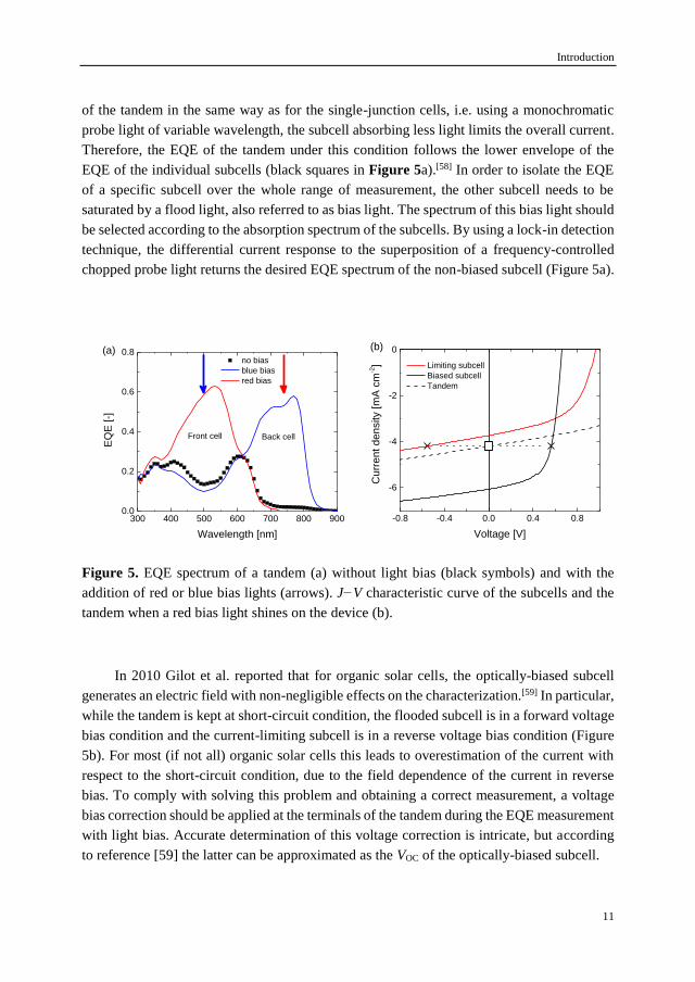
Introduction
11
of the tandem in the same way as for the single-junction cells, i.e. using a monochromatic
probe light of variable wavelength, the subcell absorbing less light limits the overall current.
Therefore, the EQE of the tandem under this condition follows the lower envelope of the
EQE of the individual subcells (black squares in Figure 5a).[58] In order to isolate the EQE
of a specific subcell over the whole range of measurement, the other subcell needs to be
saturated by a flood light, also referred to as bias light. The spectrum of this bias light should
be selected according to the absorption spectrum of the subcells. By using a lock-in detection
technique, the differential current response to the superposition of a frequency-controlled
chopped probe light returns the desired EQE spectrum of the non-biased subcell (Figure 5a).
300 400 500 600 700 800 9000.0
0.2
0.4
0.6
0.8
EQ
E [-]
Wavelength [nm]
no bias
blue bias
red bias
Front cell Back cell
(a)
-0.8 -0.4 0.0 0.4 0.8
-6
-4
-2
0
Cu
rre
nt
den
sity [
mA
cm
-2]
Voltage [V]
Limiting subcell
Biased subcell
Tandem
(b)
Figure 5. EQE spectrum of a tandem (a) without light bias (black symbols) and with the
addition of red or blue bias lights (arrows). J−V characteristic curve of the subcells and the
tandem when a red bias light shines on the device (b).
In 2010 Gilot et al. reported that for organic solar cells, the optically-biased subcell
generates an electric field with non-negligible effects on the characterization.[59] In particular,
while the tandem is kept at short-circuit condition, the flooded subcell is in a forward voltage
bias condition and the current-limiting subcell is in a reverse voltage bias condition (Figure
5b). For most (if not all) organic solar cells this leads to overestimation of the current with
respect to the short-circuit condition, due to the field dependence of the current in reverse
bias. To comply with solving this problem and obtaining a correct measurement, a voltage
bias correction should be applied at the terminals of the tandem during the EQE measurement
with light bias. Accurate determination of this voltage correction is intricate, but according
to reference [59] the latter can be approximated as the VOC of the optically-biased subcell.

Chapter 1
12
Similar considerations can be extended to the case of solar cells with more than two
junctions, as will be addressed in Chapter 4 and Chapter 5.
1.4.4 Determination of the wavelength-dependent n and k optical constants
As mentioned in Section 1.3, interference effects have an influence on the absorption
behavior of the active layers in a multiple-stack device. Optical modeling simulations allow
to estimate the fraction of absorbed photons in each layer of a specific sequence, taking into
account reflection and transmission at the interface between adjacent layers. As will become
clear when reading Chapters 3-6, this tool is particularly useful to find the optimal thickness
of the subcells in a multi-junction cell that gives high and balanced absorption of light. It
further allows to estimate the EQE spectrum of these subcells and to determine the IQE
(discussed in Section 1.3). The wavelength-dependent refractive index n(λ) and extinction
coefficient k(λ) are used as input for such simulations and it is therefore very useful to
estimate them for all the layers in the stack of interest. The following procedure focuses on
the determination of these constants for the active layers. For other materials used in
interlayers and electrodes the n and k are readily available from literature, since they are
frequently used.
To determine n(λ) and k(λ), polymer:acceptor blend layers were spin-coated on quartz
substrates and the reflectance and transmittance of the films was measured perpendicular to
the surface. The reflectance spectra (R(λ)) of the layers were used to correct the transmittance
spectra (T(λ)), resulting in the corrected transmission T′ = T/(1−R) of the layers.
Subsequently, the thickness d of the layers was measured with a profilometer and used to
evaluate the extinction coefficient k as: k(λ) = −λ ln(T′(λ))/(4πd). The calculation of the
refractive index n(E) as function of the energy E was implemented in a Python script,
following the Kramers-Kronig relation: n(E) −1 = (2/π) P∫E′ k(E′)/(E′2 – E2) dE′.
Compared to ellipsometry, widely used to determine the optical constants, this
approach does not involve a tedious and time-consuming fitting of the experimental data with
a model. On the other hand, ellipsometry allows to determine the n and k components parallel
to the plane of the layer, which can be relevant in case of anisotropy and when the angle
between the direction of light and the inward surface normal is non-zero. For the studies
involved in this thesis, where devices are illuminated at zero angle, analyzing the reflectance
and transmittance suffices. Moulé and Meerholz already addressed the problem of
determining n(λ) and k(λ) using UV/vis measurements, although in a slightly different way,
and they pointed out the criticalities for which ellipsometry provided less accurate
estimations than their method.[60]
To account for interference effects in the absorber layer on quartz, the optical constants
were determined for three different layer thicknesses and subsequently averaged to obtain the
k(λ) and n(λ) spectra. Although the averaging does not provide a rigorous solution to the
Introduction
13
problem, it provided satisfactory results in terms of modeling the optical absorption of
complex layer stacks, as demonstrated previously, see Refs. [56] and [61].
1.5 Aim and outline of the thesis
The goal of this thesis is to advance in the design, manufacturing, modeling and
characterization of multi-junction polymer solar cells.
Recent trends in the field covering the time lapse between 2015 and 2018 are reported
in Chapter 2. The development of new functional materials for the interconnecting layers and
the photoactive layers represents a significant part of the reported results. Also studies that
focus on manipulating the optical electric field in the device to enhance light absorption are
reviewed next to an overview on the characterization practices. As processing of the multi-
layers stacks is challenging new processing methods and industry-oriented applications are
described.
The first problem which was tackled was the development of a processing technique of
the ICL to fabricate inverted tandem and triple-junction solar cells with good versatility, i.e.
compatible with numerous chemically different active layer materials as subcells without the
need to constantly adopt choice of layers or choice of processing conditions to the specific
characteristics of the photoactive layer. The solution to this is provided in Chapter 3. Suitable
formulations of PEDOT:PSS and ZnO nanoparticles as charge transport materials in solvent
mixtures have been developed that allow for sufficient wetting and spreading during
deposition drying and at the same time fulfill the requirement of orthogonality, implying that
during deposition of the second layer, the first layer is not re-dissolved. In this way six
different tandem cells and three triple-junction solar cells involving a variety of active layers
could be made with the same ICL without adjusting the deposition conditions.
Triple-junction organic solar cells represent an intriguing kind of device for the high
efficiency they can achieve. In order to perform a correct characterization, the peculiarity of
OPV materials should be taken into account, to not overestimate the efficiency. Chapter 4
presents a detailed characterization protocol to fulfill this task, and shows the corresponding
results on a state-of-the-art triple-junction device with a PCE of 10.0%. The method used is
based on opto-electrical modeling simulations and measurements on representative single-
junction cells and provides an excellent match between experimental and modeled J−V and
EQE data.
To further extend the spectral response of triple-junction cells, another absorber
material was stacked on top of the back cell, with an ultralow band gap of ca. 1.1 eV. The
result, presented in Chapter 5, represents the first example ever reported of solution-

Chapter 1
14
processed quadruple-junction organic solar cell with four complementary absorber layers.
Opto-electrical modeling was involved to optimize the performance. The processing of the
ICL developed in Chapter 3 was used to interconnect all the subcells, and the characterization
protocol reported in Chapter 4 was extended to characterize the EQE of the four individual
subcells. The PCE of this cell equals 7.6%, only slightly less than the modeled value of 8.2%.
The versatile deposition technique reported in Chapter 3 allows to fabricate exclusively
inverted configuration devices. In a conventional device PEDOT:PSS would be processed on
top of a zinc oxide layer. Unfortunately the acidic dispersion from which PEDOT:PSS is
processed is not compatible with zinc oxide. In Chapter 6, commercial tin oxide colloidal
dispersions were combined with PEDOT:PSS to form new ICLs for tandems. Both
conventional and inverted tandem solar cells were manufactured with these materials, by
changing the sequence in which these were processed. Both tandem cell configurations
afforded PCEs of more than 10%.

Introduction
15
[1] United Nations. Department of Economic and Social Affairs, Population Division.
World Population Prospects: The 2017 Revision, Key Findings and Advance Tables.
Working Paper No. ESA/P/WP/248. 2017.
[2] J. Goldemberg, World energy assessment; United Nations Development
Programme: New York, NY, 2000.
[3] A. E. Becquerel, Comptes Rendus 1839, 9, 561.
[4] “April 25, 1954: Bell Labs Demonstrates the First Practical Silicon Solar Cell”. APS
News. American Physical Society. 18 (4). April 2009.
[5] D. M. Chapin, C. S. Fuller and G. L. Pearson, J. Appl. Phys. 1954, 25, 676.
[6] K. Yoshikawa, H. Kawasaki, W. Yoshida, T. Irie, K. Konishi, K. Nakano, T. Uto,
D. Adachi, M. Kanematsu, H. Uzu, K. Yamamoto, Nat. Energy 2017, 2, 17032.
[7] International Technology Roadmap for Photovoltaic Results 2017, Ninth edition,
March 2018.
[8] N. S. Lewis, Science 2007, 315, 798.
[9] National Renewable Energy Laboratory, Photovoltaic Efficiency chart, available at:
https://www.nrel.gov/pv/; accessed on 5 September 2018.
[10] M. A. Green, Third Generation Photovoltaics, Springer, 2003, ISBN: 3-540-40137-
7.
[11] C. K. Chiang, C. R. Fincher, Y. W. Park, A. J. Heeger, H. Shirakawa, E. J. Louis,
S. C. Gau, A. G. MacDiarmid, Phys. Rev. Lett. 1977, 39, 1098.
[12] H. Shirakawa, E. J. Louis, A. G. MacDiarmid, C. K. Chiang, A. J. Heeger, J. Am.
Chem. Soc., Chem. Commun. 1977, 16, 578.
[13] R. Søndergaard, M, Hösel, D. Angmo, T. T. Larsen-Olsen, F. Krebs, Mater. Today
2012, 15, 36.
[14] A. Reale, L. La Notte, L. Salamandra, G. Polino, G. Susanna, T. M. Brown, F.
Brunetti, A. Di Carlo, Energy Technol. 2015, 3, 385.
[15] M. Kaltenbrunner, M. S. White, E. D. Glowacki, T. Sekitani, T. Someya, N. S.
Sariciftci, S. Bauer, Nat. Commun. 2012, 3, 1772.
[16] R. Ma, J. Feng, D. Yin, H.-B. Sun, Org. Electron. 2017, 43, 77.
[17] Y. W. Li, G. Y. Xu, C. H. Cui, Y. F. Li, Adv. Energy Mater. 2018, 8, 1701791.
[18] K.-S. Chen, J.-F. Salinas, H.-L. Yip, L. Huo, J. Hou, A. K.-Y. Jen, Energy Environ.
Sci. 2012, 5, 9551.
[19] C.-C. Chen, L. Dou, J. Gao, W. H. Chang, G. Li, Y. Yang, Energy Environ. Sci.
2013, 6, 2714.
[20] J. Min, C. Bronnbauer, Z.-G. Zhang, C. Cui, Y. N. Luponosov, I. Ata, P. Schweizer,
T. Przybilla, F. Guo, T. Ameri, K. Forberich, E. Spiecker, P. Bäuerle, S. A.
Ponomarenko, Y. Li, C. J. Brabec, Adv. Funct. Mater. 2016, 26, 4543.
[21] D. Kearns, M. Calvin, J. Chem. Phys. 1958, 29, 950.
1.6 References

Chapter 1
16
[22] C. W. Tang, Appl. Phys. Lett. 1986, 48, 183.
[23] O. V. Mikhnenko, P. W. M. Blom, T.-Q. Nguyen, Energy Environ. Sci. 2015, 8,
1867.
[24] J. J. M. Halls, C. A. Walsh, N. C. Greenham, E. A. Marseglia, R. H. Friend, S. C.
Moratti, A. B. Holmes, Nature 1995, 376, 498.
[25] G. Yu, J. Gao, J. C. Hummelen, F. Wudl, A. J. Heeger, Science 1995, 270, 1789.
[26] S. Zhang, Y. Qin, J. Zhu, J. Hou, Adv. Mater. 2018, 30, 1800868.
[27] Z. Zheng, Q. Hu, S. Zhang, D. Zhang, J. Wang, S. Xie, R. Wang, Y. Qin, W. Li, L.
Hong, N. Liang, F. Liu, Y. Zhang, Z. Wei, Z. Tang, T. P. Russell, J. Hou, H. Zhou,
Adv. Mater. 2018, 30, 1801801.
[28] S. Li, L. Ye, W. Zhao, H. Yan, B. Yang, D. Liu, W. Li, H. Ade, J. Hou, J. Am. Chem.
Soc. 2018, 140, 7159.
[29] American Society for Testing and Materials (ASTM), Standard G173-03, available
at: http://rredc.nrel.gov/solar/spectra/am1.5/.
[30] W. Shockley, H. J. Queisser, J. Appl. Phys. 1961, 32, 510.
[31] S. Rühle, Sol. Energy 2016, 130, 139.
[32] A. De Vos, J. Phys. D: Appl. Phys. 1980, 13, 839.
[33] M. Hiramoto, M. Suezaki, M. Yokoyama, Chem. Lett. 1990, 19, 327.
[34] A. Yakimov, S. R. Forrest, Appl. Phys. Lett. 2002, 80, 1667.
[35] K. Triyana, T. Yasuda, K. Fujita, T. Tsutsui, Jpn. J. Appl. Phys. 2004, 43, 2352.
[36] J. Drechsel, B. Männig, F. Kozlowski, D. Gebeyehu, A. Werner, M. Koch, K. Leo,
M. Pfeiffer, Thin Solid Films 2004, 451–452, 515.
[37] B. Maennig, J. Drechsel, D. Gebeyehu, P. Simon, F. Kozlowski, A. Werner, F. Li,
S. Grundmann, S. Sonntag, M. Koch, K. Leo, M. Pfeiffer, H. Hoppe, D. Meissner,
N. S. Sariciftci, I. Riedel, V. Dyakonov, J. Parisi, Appl. Phys. A 2004, 79, 1.
[38] G. Dennler, H.-J. Prall, R. Koeppe, M. Egginger, R. Autengruber, N. S. Sariciftci,
Appl. Phys. Lett. 2006, 89, 073502.
[39] A. Colsmann, J. Junge, C. Kayser, U. Lemmer, Appl. Phys. Lett. 2006, 89, 203506.
[40] V. Shrotriya, E. H.-E. Wu, G. Li, Y. Yao, Y. Yang, Appl. Phys. Lett. 2006, 88,
064104.
[41] K. Kawano, N. Ito, T. Nishimori, J. Sakai, Appl. Phys. Lett. 2006, 88, 073514.
[42] J. Gilot, M. M. Wienk, R. A. J. Janssen, Appl. Phys. Lett. 2007, 90, 143512.
[43] J. Y. Kim, K. Lee, N. E. Coates, D. Moses, T.-Q. Nguyen, M. Dante, A. J. Heeger,
Science 2007, 317, 222.
[44] J. Gilot, M. M. Wienk, R. A. J. Janssen, Adv. Mater. 2010, 22, E67.
[45] L. Dou, J. You, J. Yang, C.-C. Chen, Y. He, S. Murase, T. Moriarty, K. Emery, G.
Li, Y. Yang, Nat. Photonics 2012, 6, 180.
[46] J. You, L. Dou, K. Yoshimura, T. Kato, K. Ohya, T. Moriarty, K. Emery, C.-C.
Chen, J. Gao, G. Li, Y. Yang, Nat. Commun. 2013, 4, 1446.
Introduction
17
[47] C.-H. Chou, W. L. Kwan, Z. Hong, L.-M. Chen, Y. Yang, Adv. Mater. 2011, 23,
1282.
[48] J. Yang, R. Zhu, Z. Hong, Y. He, A. Kumar, Y. Li, Y. Yang, Adv. Mater. 2011, 23,
3465.
[49] Y. Zhou, C. Fuentes-Hernandez, J. W. Shim, T. M. Khan, B. Kippelen, Energy
Environ. Sci. 2012, 5, 9827.
[50] J. Jo, J.-R. Pouliot, D. Wynands, S. D. Collins, J. Y. Kim, T. L. Nguyen, H. Y. Woo,
Y. Sun, M. Leclerc, A. J. Heeger, Adv. Mater. 2013, 25, 4783.
[51] D. W. Zhao, X. W. Sun, C. Y. Jiang, A. K. K. Kyaw, G. Q. Lo, D. L. Kwong, IEEE
Electron Device Lett. 2009, 30, 490.
[52] Y. Zou, Z. Deng, W. J. Potscavage, M. Hirade, Y. Zheng, C. Adachi, Appl. Phys.
Lett. 2012, 100, 243302.
[53] J. Gilot, Polymer Tandem Solar Cells, Ph.D. thesis, Eindhoven University of
Technology, 2010, ISBN: 978-90-386-2279-8.
[54] Heliatek, available at: http://heliatek.com.
[55] S. Esiner, H. Van Eersel, M. M. Wienk, R. A. J. Janssen, Adv. Mater. 2013, 25,
2932.
[56] W. Li, A. Furlan, K. H. Hendriks, M. M. Wienk, R. A. J. Janssen, J. Am. Chem. Soc.
2013, 135, 5529.
[57] C.-C. Chen, W.-H. Chang, K. Yoshimura, K. Ohya, J. You, J. Gao, Z. Hong, Y.
Yang, Adv. Mater. 2014, 26, 5670.
[58] R. Timmreck, T. Meyer, J. Gilot, H. Seifert, T. Mueller, A. Furlan, M. M. Wienk,
D. Wynands, J. Hohl-Ebinger, W. Warta, R. A. J. Janssen, M. Riede, K. Leo, Nat.
Photonics 2015, 9, 478.
[59] J. Gilot, M. M. Wienk, R. A. J. Janssen, Adv. Funct. Mater. 2010, 20, 3904.
[60] A. J. Moulé, K. Meerholz, Appl. Phys. Lett. 2007, 91, 061901.
[61] C. Duan, A. Furlan, J. J. van Franeker, R. E. M. Willems, M. M. Wienk, R. A. J.
Janssen, Adv. Mater. 2015, 27, 4461.

Chapter 2
Recent Developments on Solution-Processed
Multi-Junction Organic Solar Cells*
Abstract
This chapter offers an overview of the recent (2015 to mid-2018) developments in the
field of solution-processed multi-junction organic solar cells. In this time lapse different
strategies have been investigated to improve the performance of these devices. An important
one involves the development of new materials and processing methods for the photoactive
layers and the interconnecting layers. In addition, specific layers or combinations thereof
have been conveniently adopted to increase light absorption and improve the photocurrent
by utilizing optical interference effects that play a key role in these multi-junction
semitransparent thin layer stacks. Together with the increase in power conversion efficiency,
accurate characterization procedures are required to keep a critical view on the results and
new insights in this matter are discussed. Application of multi-junction cells for
photoelectrochemical water splitting and upscaling towards a commercial technology are
briefly addressed.
* This chapter has been submitted for publication as part of: D. Di Carlo Rasi, R. A. J.
Janssen. Advances in Solution-Processed Multi-Junction Organic Solar Cells.

Chapter 2
20
2.1 Introduction
In this chapter recent developments in the field of solution-processed organic tandem
solar cells are discussed.† The topic was last reviewed in 2015 and since then significant
progress has been made.[1-8] The materials forming the interconnecting layer (ICL) are key to
the optimal performance of tandem cells. The ICL serves to connect the subcells, both
optically and electrically, preferably without losses. Optical transparency, uniformity,
mechanical robustness, solvent orthogonality during processing, matching with the relevant
HOMO and LUMO levels and Ohmic character are important requisites that the ICL has to
fulfill. Besides the specific materials choice, the processing of the ICL from a liquid medium
plays a decisive role in the success of manufacturing the multi-layer stacks. Co-solvents,
additives, blends, and deposition techniques in general are commonly explored factors to
tweak the characteristics of the ICL. Because the absorber and ICL films are semitransparent
thin layers, interference effects play an important role in the distribution of the optical electric
field in the subcells and in turn in the absorption of light and the generated photocurrent.
Different approaches like the insertion of a thin reflecting materials inside the ICL can alter
the distribution of the optical field, to achieve a better balance in current generation. As
discussed in Chapter 1, tandem solar cells require photoactive materials with different band
gaps. In the context of solution-processed organic photovoltaic (OPV), the absorbers consists
of semitransparent thin films which can have a substantial overlap of their absorption spectra.
Hence, in addition to having different band gaps, photoactive layers should preferably also
have complementary absorption spectra, such that high energy photons that pass the first
layer are not absorbed in the second layer and are reflected at the back electrode. The optimal
thickness of single-junction cells is known to be limited by bimolecular recombination.
Developing photoactive absorber blends with thickness-insensitive performance can alleviate
the disadvantages of spectral overlap between the two subcells and increase the photocurrent.
Moreover, a high external quantum efficiency (EQE) is a prerequisite to absorb the incident
photons and increase the short-circuit current density (JSC). To afford a high open-circuit
voltage (VOC) tandem, both the subcells should possess a low minimum photon energy loss
(Eloss), defined as the difference between their optical band gap (Eg) and eVOC. Recombination
mechanisms should also be kept under control mainly via the creation of a suitable blend
morphology. A significant part of this chapter addresses recent developments of tandem solar
cells where new combinations of photoactive materials are presented. Although not yet
mature for the market, solution-processed tandem OPV technology was studied also related
to industry-oriented aspects such as the processing under ambient atmosphere, the increase
† The results presented in this chapter are largely based on a search on Web of Science, using the keywords:
“TI=((tandem OR triple* OR (multi*junction*) OR (multi-junction*)) AND (organic OR polymer OR (small
molecul*) OR (non-fullerene) OR (*fullerene*) OR (*fullerene-)) AND ((solar cell*) OR photovoltaic* OR
(photovoltaic cell*))) AND PY=(2015-2018)”, limited to the period from January 2015 to August 2018. Articles about hybrid tandem solar cells, articles where no actual device was fabricated and out-of-topic entries were
excluded.

Recent Developments on Solution-Processed Multi-Junction Organic Solar Cells
21
in device area by interconnecting more tandem cells to make a module, and the processing
from solution of the electrodes. The combination of more than two absorbers in solution-
processed multi-junction solar cells is still object of research, aiming at a further increase in
efficiency with respect to tandems. Overall, the reliability of the OPV field hinges on accurate
characterization protocols, taking into account the peculiarities of organic photovoltaic
materials. A detailed protocol for this was published at the beginning of the time period
covered here, and a brief analysis of how researchers now use the protocol is presented. Some
newly-developed exotic device stacks that do not fall in the category of tandems are included.
Besides the clear interest in increasing the power conversion efficiency (PCE) over that of
single-junction devices, specific applications can be identified where the properties of OPV
tandem cells turn advantageous. Photoelectrochemical water splitting is one of them, because
OPV tandem cells can provide the necessary voltage at the operating point. This voltage
should exceed the standard potential of 1.23 V for the water splitting reaction plus the
overpotentials at the electrodes. Conclusive general considerations complete the chapter. An
overview of the relevant features of the tandem cells published in the covered period is
collected in Table 1.
2.2 Tandem solar cells
2.2.1 ICL materials
The ICL generally consists of combinations of polymeric and metal oxide materials.
Poly(3,4-ethylenedioxythiophene):polystyrene sulfonate (PEDOT:PSS) as hole transporting
layer (HTL) and zinc oxide nanoparticles as electron transporting layer (ETL) remain a
widely adopted combination of materials. From Table 1, it emerges that also evaporated
molybdenum oxide (HTL), followed by a thin (discontinuous) layer of silver and poly[(9,9-
bis(3′-(N,N-dimethylamino)propyl)-2,7-fluorene)-alt-2,7-(9,9-dioctylfluorene)] (PFN) as
ETL are frequently used. Nevertheless, several new materials have been introduced in recent
years. Especially, conjugated polyelectrolytes (CPE) and structurally related pH-neutral self-
doped conductive polymers (SCPs) are a largely explored alternative both for the p- as well
as for the n-type charge transporting layers. Decorating a conjugated polymer with anionic
or cationic side groups can create dipole moments that change the work function of the
substrate on which they are coated. The CPEs are often wide band gap semiconducting
materials that serve to change the work function. CPEs and SCPs are typically used as thin
layers (< 25 nm) to reduce parasitic light absorption. Generally, CPEs are processed from
alcoholic solvents because these are compatible with most of the tandem stacks. Figure 1
provides the chemical structure of the materials discussed hereafter.

Chapter 2
22
Figure 1. Materials adopted in the ICL of tandem solar cells covered by this chapter. The
references for publications using these materials are provided in Table 1.
In 2015, Zhou et al. presented two new CPEs: PCPDTBTSO3K (CPE-K) and
PCPDTPhSO3Na (CPEPh-Na).[9] Owing to the ionic side groups, a thin layer (10−15 nm) of
these p-type materials could effectively increase the work function of the substrate to 5.2 eV.
Tandem devices using a zinc oxide nanoparticles layer coated with CPEPh-Na as ICL showed
PCE up to 11.3%. Structurally similar is the p-type CPE PCP-Na, adopted by Cui et al. in

Recent Developments on Solution-Processed Multi-Junction Organic Solar Cells
23
2017.[10] An ICL of zinc oxide nanoparticles and PCP-Na allowed the realization of over 13%
PCE in tandems with state-of-the-art photoactive materials. An interesting CPE in this series
is p-PFP-O, used in a tandem device by Lee et al. in 2016.[11] p-PFP-O derives from the
oxidative doping of its n-type counterpart (PFP-O), by treating the latter with ammonium
persulfate. As consequence of the oxidation, the orientation of the dipole moment is reversed,
with respect to PFP-O. The authors successfully demonstrated the good performance (PCE
ca. 10%) of this CPE in a tandem cell with a zinc oxide/PEDOT-SO3Na/p-PFP-O ICL, where
PEDOT-SO3Na is a pH-neutral form of PEDOT. pH-neutral PEDOT has a low work function
and to avoid loss in VOC, the p-PFP-O was used. In 2016 Zhang et al. presented PF3N-2TNDI
as a useful CPE for the n-type side of an ICL in combination with PEDOT:PSS on the p-side
and a ultra-thin silver layer in between.[12] The role of silver is to provide a recombination
center for charges from the subcells, thanks to its high conductivity. PF3N-2TNDI could
reduce the work function of silver down to 4.1 eV. The CPE proposed by Zhang et al.
outperformed the well-known PFN, not only in terms of PCE but also as reduced dependence
of the performance on its thickness (PCE still 9.7% at 20 nm). The same group demonstrated
in 2018 that by mixing PF3N-2TNDI with polyethyleneimine (PEI), the work function could
be further lowered without significantly affecting charge transport. [13,14] With the optimal
mixed ETL, a high performing tandem could be fabricated without the need of the silver layer
in between ETL and PEDOT:PSS. The tandem with this mixed ETL could afford a PCE of
11%, even at 70 nm thickness of the ETL (the optimal PCE was 12.6% at 20 nm of
thickness).[13] A good performance for tandems adopting PFN was reported independently by
Zuo et al.[15] and Martinez-Otero et al.[16], both in 2015. The ICL used consisted of evaporated
molybdenum oxide with an ultra-thin layer of silver and PFN on top. PCEs approaching
11%[15] and an extraordinarily high FF of 0.76[16] were achieved. Even with a total thickness
below 20 nm,[16] the ICL provided the necessary protection of the front cell from processing
of the back cell on top, and good optical transparency. Continuing with the n-type CPEs, Lu
et al. demonstrated a novel ICL consisting of an all-solution-processed metal oxide/dipole
layer/metal oxide stack.[17] PF6N25Py was used to make a layer on top of another layer of
molybdenum bronze. The work function of the latter was effectively lowered, improving the
energy level alignment with a subsequent film of titanium dioxide nanoparticles.[17] By
fabricating homo tandems with this ICL, a correct addition of the VOC of the subcells was
obtained, together with comparable FF to the single-junction reference cell and improved
overall efficiency.
Metal oxides are a very popular class of interlayer materials for electronics in general
and for OPV as well. Metal oxides commonly adopted in OPV are deposited either from pre-
formed nanoparticles suspensions, from a metal-organic precursor in solution which converts
to some extent to a metal oxide, or via thermal evaporation in high vacuum. Concerning their
use in solution-processed tandem solar cells, it is worth to mention that examples of all-oxide
ICLs are rare in general and always involve the presence of thin metal clusters to improve
Chapter 2
24
their conductivity.[18,19] Only in 2018 Becker et al. reported the first all-oxide ICL for polymer
tandem solar cells.[20] A possible reason for the scarcity of such examples might be because
very few materials (like PEDOT:PSS) can guarantee the protection of the front cell active
layer against the processing from solution of the back cell active layer.[21] The exceptional
example of Becker et al. consisted of an inverted (n-i-p) configuration tandem in which
thermally evaporated molybdenum oxide (HTL) and tin oxide (ETL) deposited via atomic
layer deposition were stacked together to form the ICL. Together with the singular protection
against solvents, the authors indicated that a large intrinsic interface dipole at the interface
HTL/ETL makes the conduction bands of molybdenum oxide and tin oxide to align. In
addition, the tandem featuring this ICL did not suffer from the well-known problem of
necessity of UV light soaking. In fact, it is known that exposing common conductive metal
sub-oxides, such as zinc oxide and titanium dioxide, to UV light illumination can increase
their conductivity by a photodoping mechanism.[ 22 ] In Chapter 6, the use of solution-
processable tin oxide nanoparticles suspensions for OPV tandems is presented for the first
time.[23] In combination with PEDOT:PSS as HTL, both conventional (p-i-n) and inverted
architecture tandems were realized using only these two materials, with performance in good
agreement with the expectations. For conventional tandems tin oxide offers the possibility to
avoid the use of pH-neutral PEDOT:PSS, which can cause a loss in VOC due its reduced work
function. In fact, tin oxide proved to be resistant against the acidity of the commercial
formulation of PEDOT:PSS (Al 4083), while zinc oxide is washed away. In 2015 Mitul et al.
implemented solution-processed aluminum-doped zinc oxide (AZO) in a
PEDOT:PSS/AZO/PEIE ICL, where PEIE is the partially ethoxylated polyethyleneimine.[24]
Thermal annealing at 150 °C was required to form AZO from its precursor. To demonstrate
the proper working of this ICL, the authors built a homo tandem using P3HT:PCBM, which
can sustain this temperature. In 2017 Du et al. reported molybdenum oxide nanoparticles as
a solution to overcome interfacial losses occurring in some tandem solar cells where
PEDOT:PSS is used as HTL.[25] They attributed poor hole transporting properties of the
interface between PEDOT:PSS and an active layer with polymers containing nitrogen atoms
to the protonation of the latter. By mixing PEDOT:PSS and MoO3 nanoparticles, the problem
was reported to be solved and tandem solar cells using a PEDOT:PSS:MoO3/ZnO/PEI ICL
showed improved performance compared to the control tandem devices with only
PEDOT:PSS or MoO3. Concerning composite materials with PEDOT:PSS, Torabi et al.
reported in 2015 a mixture of modified PEDOT:PSS and silver nanoparticles as HTL in the
ICL, in combination with sol-gel titanium dioxide as ETL.[26] The silver nanoparticles were
synthesized directly in the dispersion of the modified PEDOT:PSS by reduction of the silver
nitrate precursor with sodium borohydride, without the need of a stabilizer. A homo tandem
was realized to check the performance. The VOC was 1.1 V and the FF 0.60, against the 0.59
V and FF of 0.55 of the reference cell.
Recent Developments on Solution-Processed Multi-Junction Organic Solar Cells
25
Recently, few examples of tandem solar cells have emerged in which metal-organic
compounds have been adopted in the ICL. Lu et al. in 2016[27] and Chang et al. in 2017[28]
adopted zirconium acetylacetonate (Zr-acac) to lower the work function of PEDOT:PSS in
the ICLs: PEDOT:PSS/Zr-acac/PF6N25Py and MoO3/PEDOT:PSS/Zr-acac, respectively.
Zr-acac has the advantage that it can be easily processed from solution and does not require
a thermal annealing treatment. Another example of metal chelate in tandems was published
in 2018 by Shi et al.[29] In their work, Shi et al. used titanium (diisopropoxide)bis(2,4-
pentanedionate (TIPD) on top of evaporated MoO3/Ag as ICL, applying a post-treatment of
150 °C to get the optimal performance of the tandem. A single example of an inorganic
transition metal compound for tandem applications is represented by the phosphomolybdic
acid hydrate (PMA), presented by Lu et al. in 2017 in both conventional and inverted
structure tandems.[30] In their work, a modified pH-neutral PEDOT:PSS layer served as
recombination center for the charges extracted by the PMA HTL and the zinc oxide
nanoparticles ETL. The ICL was then PMA/PEDOT:PSS/ZnO in inverted tandems and vice
versa for the conventional ones. As will be discussed in more detail in Chapter 6, the work
function of pH-neutral PEDOT:PSS does not match the deep-lying HOMO energy level of
some photoactive polymers, generally provoking a loss in VOC.[31] By using PMA in between
pH-neutral PEDOT:PSS and the active layer of P3HT:PC60BM the authors showed a
recovery in the VOC with respect to the control device without PMA (0.62 V vs 0.48 V,
respectively).
Concerning the use allotropic forms of carbon in the ICL, three examples have been
reported in the last period. In 2015 Chang et al. used a cross-linkable azidofullerene
derivative ((C-)PCBN3), doped with tetrabutylammonium iodide (TBAI) as ETL, on top of
PEDOT:PSS.[32] A temperature of 140 °C was used for the curing of the ETL, which allowed
the manufacturing of tandems on a flexible polyethylene naphthalate substrate with good
performance (PCE of 8.7% vs 9.3% on glass). The ETL showed also a weak thickness
dependence of the performance, with an optimum at 10 nm. A mixture of PEDOT:PSS and
graphene oxide has been reported to work in an ICL, together with lithium-doped zinc oxide
(LZO) as ETL, in a publication published in 2015 by da Silva et al.[33] Another form of carbon
for the ICL are carbon quantum dots (CQDs), mixed with PEI described by Kang et al. in
2018.[34] CQDs were synthesized by a microwave reaction starting from citric acid and β-
alanine, resulting in particles with size of ca. 3 nm. A thin layer of the CQDs/PEIE composite
on top of PEDOT:PSS was reported to provide an efficient tunneling junction for the
recombination of charges in the ICL, affording a best efficiency of 12.1%.
2.2.2 Processing multi-junction stacks
For the commercial success of future tandem OPV technology is important to simplify
the manufacturing processes as much as possible. In this section recent advances focusing on
processing of tandem OPV cells are reported.

Chapter 2
26
Lee et al.[11,35,36] adapted a concept first introduced by Wei et al.[37] for single-junction
OPV devices to tandem solar cells. The idea is to process both the photoactive components
and interlayer material from the same solution. By taking advantage of different surface
energy of these components, a favorable spontaneous segregation of the interlayer materials
at the desired interfaces can take place during the deposition (Figure 2). In their tandem
devices, Lee et al. mixed either PEI[35,36] or p-PFP-O[11] with the active layer blend materials.
For the latter, they choose a widely reported combination: PTB7-Th as electron donor and
PC70BM as electron acceptor. Inverted[35,36] and conventional[11] tandems were demonstrated
using this technique to process both the front and the back subcells, where the ICL was either
PEDOT:PSS/PEI[35,36] or zinc oxide/PEDOT-SO3Na/p-PFP-O.[11] Time-of-flight secondary-
ion mass spectrometry measurements confirmed the localization of PEI at two positions
(bottom and top subcells) along the vertical direction of the stack, rather than being uniformly
distributed.
Figure 2. Tandem polymer solar cell processed from bulk heterojunction:PEI nanocomposite
solution. Reproduced with permission from Ref. 35. Copyright 2014 WILEY-VCH Verlag
GmbH & Co. KGaA, Weinheim.
Recent reports focused on the improved processing of the traditional combination
PEDOT:PSS/zinc oxide as ICL for inverted tandem solar cells. In 2017 Chen et al. reported
the processing of diethyl zinc precursor on top of a “wet” (not annealed) layer of PEDOT:PSS
as ICL.[38] According to the authors, the residual moisture in the PEDOT:PSS film promoted
the conversion of the precursor to zinc oxide. The as-formed layer of zinc oxide only needed
a mild thermal annealing at 80 °C, which was compatible with the front cell active layer. As
a result a record 2.16 V of VOC, combined with a 10.2% efficiency were achieved in a tandem

Recent Developments on Solution-Processed Multi-Junction Organic Solar Cells
27
device, demonstrating the good functioning of the ICL. Given the hydrophobic nature of
commonly adopted active layer materials, the deposition of a layer of PEDOT:PSS from an
aqueous dispersion requires the use of surfactants to lower the surface energy. Surfactants
are in general insulating and the amount of them necessary to improve the casting can
eventually be substantial and deteriorate the desired properties of PEDOT:PSS. Moreover,
modifying PEDOT:PSS might affect unfavorably the distribution of the insulating PSS part,
creating an energy barrier. In 2016 Prosa et al. proposed a simple approach to recover the
good functioning of a PEDOT:PSS film deposited from a suspension including a surfactant
(Zonyl FS-300).[39] By simply rinsing the film with isopropanol, part of the surfactant and the
excess of PSS at the surface of the layer could be removed. Tandems with isopropanol-rinsed
PEDOT:PSS, followed by zinc oxide nanoparticles as ICL demonstrated optimal
performance, contrary to the pristine device with non-rinsed PEDOT:PSS. In fact, the latter
featured an s-shape in the J–V characteristics, likely denoting the presence of an interfacial
barrier. The results discussed in the Chapter 3 of this thesis[40] demonstrate how both the
requirements of a low annealing temperature of the ICL and a low surface energy of the
PEDOT:PSS dispersion can be satisfied at the same time. It was found that by processing in
inert atmosphere the commercial formulation of PEDOT:PSS (Al4083) from a mixture of
water/1-propanol (1:2 v/v) provides a good coverage for a wide selection of different active
layer materials, without the need of a surfactant. A synthetic procedure of zinc oxide
nanoparticles was also reported, and isoamyl alcohol was adopted as liquid for the dispersion.
The processing of zinc oxide from such suspension did not negatively affect the PEDOT:PSS
layer. Without any thermal annealing treatment, the proposed processing technique afforded
six tandems and three triple-junction solar cells featuring eight active layer materials of
different chemical nature. Using the same technique, the first example of a solution-processed
quadruple-junction polymer solar cell with four complementary absorber layers was reported,
discussed in detail in Chapter 5.[41]
Orthogonality of the solutions is a stringent requirement for fabricating complex device
stacks such as tandems directly from solution. A possible way to get around this constraint is
to stamp transfer the top subcell, avoiding the use of solvents. In 2017 Ka et al. demonstrated
an example of device fabricated in this fashion. In their work they deposited a front cell
consisting of the small molecular donor TAPC blended with C70.[42] Next in the stack they
deposited, also by thermal evaporation, a PTCBI:C70 buffer electron transport layer,
preceding a PTCBI/Ag/HAT-CN interconnecting layer. For the back cell they adopted
PCPDTBT:PC70BM, which has a low band gap of 1.38 eV. The latter was deposited by spin-
coating onto a poly(dimethylsiloxane) stamp, dried in high vacuum from solvents, coated
onto the evaporated front subcell/ICL stack and detached from the stamp after annealing at
100 °C under applied pressure, to form a conformal contact at the interface. The resulting
tandem was characterized by a correct addition of the VOC of the subcells: this was 0.89 and
0.59 V for the front and the back subcells respectively, while for the tandem 1.46 V of VOC

Chapter 2
28
was measured. Maybe due to the limited FF of both the single-junction cells, the tandem
featured a FF of only 0.51, limiting the efficiency to 6.26%. Later, in 2018 Ka et al. also
demonstrated a polymer tandem solar cell where both the front and the back subcells were
deposited by stamp transfer and the interlayers were obtained by thermal evaporation.[43]
P3HT:PC60BM was adopted in the front cell and PCPDTBT:PC70BM as back cell. The
tandem showed full addition of the VOC (1.20 V) and a FF of 0.60. In 2018, Che et al. revisited
the same concept of combining a thermally evaporated front cell together with a solution-
processed back cell.[44] Differently from the work discussed before, the back subcell was
directly deposited by spin-coating on top of the evaporated front subcell. The former was a
DTDCPB:C70 co-evaporated cell, coated with ETL BPhen:C60/Ag, also by thermal
evaporation. Following, PEDOT:PSS was cast to complete the ICL, and the back cell of
PTB7-Th:BT-CIC was deposited by spin-coating. The front cell donor material has a wide
band gap of 1.68 eV, while donor and acceptors in the back cell have band gaps of 1.58 and
1.38 eV, respectively. An outstanding high PCE of 15 % was obtained by this tandem cell,
arising from an EQE between 70% and 80%, corresponding to a measured JSC of 12.7 mA
cm−2. By applying an antireflection coating on the glass facade the JSC increased even further,
up to 13.3 mA cm−2. In addition, the VOC of 1.59 V followed the sum of the constituent
subcells (0.90 and 0.69 V for the front and back cells, respectively), together with a high FF
of 0.71. Another remarkable aspect of this work is the high yield accompanying the high
efficiency: 97% and 95% for solar cells with active area of 2 and 9 mm2, from a total of 130
devices.
2.2.3 Light management
Organic multi-junction solar cells feature stacks of several semitransparent thin films.
For such kind of devices, optical interference effects play an important role, reason for which
a number of papers have focused their attention on how to take advantage of these effects, in
order to improve the balance of absorption of light from the two subcells. In 2015 Zuo et al.
explored the influence of the thickness of the Ag layer in a MoO3/Ag/PFN ICL on the balance
of current from the subcells.[15] In particular, an optical micro-cavity is formed between the
thin silver layer in the ICL (8−14 nm) and the opaque silver contact on the back cell (Figure
3).

Recent Developments on Solution-Processed Multi-Junction Organic Solar Cells
29
Figure 3. Micro-cavity tandem polymer solar cell. Device scheme (a), cartoon
illustrating the micro-cavity enhancement in the back cell (b), and modeled EQE spectra of
the subcells as function of the thickness of the Ag layer in the ICL. Reproduced with
permission of RSC, from Ref. 15 conveyed through Copyright Clearance Center, Inc.
By acting on the thickness of the thin silver layer, the balance of absorption between
front and back subcells could be tuned to achieve current matching. Moreover, the authors
were able to measure the individual subcells directly by accessing externally the intermediate
silver contact. A similar phenomenon was observed in tandem cells with parallel-connection
by Lee et al. in 2015[45] and Zuo et al. in 2017.[46] In the first case MoO3/Ag/MoO3 was the
ICL, while in the second case it was PEDOT:PSS/Ag/Au/MoO3. In a parallel-connection
tandem the requirement of current matching drops, since the total current is the summation
of the current of the subcells. Besides the increase in current, the voltage is pinned to the
lowest voltage between the two subcells. Due to the limited charge mobility in most of the
organic semiconductors, the optimal thickness of a single-junction device is usually
determined by the tradeoff between increasing charge generation by more light absorption in
thicker layers and the concomitant decrease because of bimolecular charge recombination.
To increase light absorption while preserving the fill factor (influenced by charge
recombination), the same active layer absorber can be deposited twice in a homo tandem.
The one reported by Zuo et al. in particular, represented at the time the most efficient example
for organic tandem solar cell with parallel connection (PCE of 11.1%). PTB7-Th:4TIC was
used as active layer. Again to improve the absorption of active layers suffering from
thickness-dependent performance, in 2015 Mantilla-Perez et al. fabricated a four-terminal
homo-tandem solar cell.[47] A glass substrate coated with indium-doped tin oxide (ITO) on
both sides was used to build single-junction cells on each side (Figure 4a).
(a) (b) (c)

Chapter 2
30
Figure 4. Four-terminal tandem (a) and top-illuminated tandem with DMD electrode (b).
Reprinted with permission from Ref. 47 (Copyright (2015) American Chemical Society) and
with permission of RSC from Ref. 48 (conveyed through Copyright Clearance Center, Inc).
As transparent electrode, a dielectric-metal-dielectric (DMD) electrode was deposited
by thermal evaporation on top of one of the active layers, consisting of MoO3/Ag/MoO3. The
top electrode on the other subcell was an opaque metal. Another advantage of this special
architecture is that the two subcells can be operated independently, which solves the
requirement of current or voltage matching. As stressed by the authors, a limiting factor in
their particular device was the DMD electrode, due to its poor transparency. Related to this
point, Zuo et al. reported in 2016 a series-connected tandem solar cell featuring a
MoO3/Ag/TeO2 DMD transparent top electrode.[48] The device was built starting from an
opaque silver layer on glass as bottom electrode, and finished with the DMD stack on top
(Figure 4b). Interestingly, the DMD tandem had a performance close to the ITO-based
counterpart, thanks to the TeO2 capping layer, which reduced the reflection at the thin silver
layer, the first one encountered by light. Another way to enhance the absorption of the active
layers was reported in 2018 by Mayer et al.[49] Here a templated periodical structure was
applied externally on the glass side of an ITO-based tandem solar cell. The structure reported
was made with a UV-curable polymer on a glass substrate and a master template fabricated
with laser interference lithography. A relative increase by 9% in the PCE was recorded
following the application of this diffractive structure.
Optical interference in tandem solar cells is usually optimized considering illumination
in the direction perpendicular to the surface of the device. Nevertheless, in practical scenarios
the solar cell is not constantly oriented in such direction but there is rather a certain angle of
incidence. In 2016 Mertens et al.[50] tried to understand a peculiar behavior of organic tandem
(a) (b)

Recent Developments on Solution-Processed Multi-Junction Organic Solar Cells
31
solar cells, already reported by Riede et al.[51] for evaporated tandem cells in 2011. In detail,
when their device was at a certain angle of orientation Θ with respect to the direction of
incidence of light, the short-circuit current density corrected by the effective area of
illumination (J*SC=JSC/cos(Θ)) was relatively insensitive to this angle, up to 65°.[50] In their
work, the authors showed that both the measured and modeled EQE spectra of the individual
subcells change according to Θ. Nevertheless, both of the corresponding spectrally integrated
J*SCs stay relatively constant. The angle-insensitivity of the performance of organic tandem
solar cells is particularly interesting for their application in realistic operating conditions.
In order for tandem organic solar cells to succeed in their commercialization, appealing
characteristics like the possibility to easily tune their color are very important. In 2017 Luo
et al. reported flexible all-solution-processed polymer tandem solar cells with different
colors.[52] Thanks to the highly conductive PEDOT:PSS top electrode, the reflectivity of the
device was engineered by simply changing the thickness of it. PCE values from 7.23 to 8.34%
were achieved, corresponding to different colors.
2.2.4 Active layer materials
In order to exploit the full potential of tandem solar cells, the active layer materials need
to be engineered to absorb light in complementary regions of the solar spectrum. A number
of materials, either newly developed or previously reported in single-junction devices, have
been adopted in tandem solar cells for this purpose. For a complete list of photoactive
materials, either small molecules or polymers, and their optical gap, the reader should refer
to Table 1. Figures 5-10 show their chemical structure.
Figure 5. Fullerene acceptors used in tandem solar cells covered by this chapter. The
references for publications describing these materials are provided in Table 1.

Chapter 2
32
Figure 6. Polymer donor materials used in tandem solar cells covered by this chapter. The
references for publications describing these materials are provided in Table 1.

Recent Developments on Solution-Processed Multi-Junction Organic Solar Cells
33
Figure 7. Additional polymer donor materials used in tandem solar cells covered by this
chapter. The references for publications using these materials are provided in Tables 1 and
2.

Chapter 2
34
Figure 8. Non-fullerene acceptor materials used in tandem solar cells covered by this chapter.
The references for publications using these materials are provided in Table 1.

Recent Developments on Solution-Processed Multi-Junction Organic Solar Cells
35
Figure 9. Donor and acceptor materials for all-polymers blends reported in tandem solar cells
covered by this chapter. The references for publications using these materials are provided in
Table 1.
Figure 10. Small molecular donor materials used in tandem solar cells covered by this
chapter. The references for publications using these materials are provided in Table 1.

Chapter 2
36
Photoactive blends based on PCBM were traditionally the most diffused and studied.
Benefiting from its isotropy, PCBM works reasonably well with a wide range of polymer
donors. PTB7-Th represents a benchmark donor material for polymer-fullerene blends in the
last years, especially for tandem solar cells. With a band gap of 1.58 V, a single-junction
device based on this material and PC70BM features a VOC around 0.8 V and efficiency up to
10% or more.[53] When blended with PC70BM, an efficiency of 11.3% was reported for a
homo-tandem device with this active layer, despite the lack of complementarity in the
absorption due to the use of the same absorber for both the front and back subcells.[9] More
groups reported similar efficiencies for tandem cells featuring this blend at least in one of the
two subcells.[34,54,55] In 2015 Zheng et al. combined the polythiophene PDCBT and the
benzodithiophene-based PBDT-TS1, blended with PC70BM and PC60BM, respectively in a
tandem device.[56] The first one has a wide band gap of 1.90 eV and the second one has a
band gap of 1.51 eV. Both possessed maximum EQEs around 70% in optimal single-junction
devices and VOCs of 0.80 V. The authors fabricated a tandem by using the PDCBT blend for
the front cell and the PBDT-TS1 blend as back cell. A PCE of 10.2% was reported for this
device. Besides a moderate FF of 0.55, the device showed a correct addition of the VOC of the
subcells (VOC = 1.60 V) and a remarkable JSC of 11.7 mA cm−2. This high value of JSC derived
from the EQE spectrum of the subcells, being as high as almost 70% (back cell) and ca. 75%
(front cell). Nevertheless some concern arises because the summed EQE of the subcells goes
above 100% around 450 nm. In 2016 the same group synthesized a new low band gap
polymer[57] by introducing fluorine atoms in the structure of the already reported PDPP4T.[58]
Compared to PDPP4T, the fluorinated version PDPP4T-2F showed a slightly broader
absorption spectrum, the onset being at ca. 900 nm. The main advantage of this new version
consists in the high VOC it can give, when mixed with PC60BM, thanks to the lower HOMO
level (0.12 eV lower). The difference in VOC of the single-junction cells reflected perfectly
the difference in HOMO: 0.78 V vs 0.66 V for PDPP4T-2F and PDPP4T, respectively. A
tandem with PBDD4T-2F:PC60BM (VOC = 0.90 V) as front cell and PDPP4T-2F:PC70BM as
back cell afforded a high VOC of 1.68 V, together with a JSC of 11.3 mA cm−2 and PCE 11.6%.
Benefitting from the successful development of benzodithiophene (BDT) based polymers,
Duan et al. reported in 2015 a thienyl-substituted BDT copolymerized with fluorine-
substituted benzothiadiazole (BT) and two thiophenes (BDT-FBT-2T).[59] The optical band
gap of this polymer amounted to 1.72 eV. Single-junction solar cells with a blend of this
polymer with PC70BM showed no loss of performance at increasing thickness of the active
layer up to 250 nm. Both these characteristics make it suitable as front cell wide band gap
donor material in a tandem device. Using PMDPP3T:PC60BM as back cell, a tandem with
PCE of 8.9% was fabricated, for which the main limiting factor was the VOC (1.42 V), due to
the significant minimum photon energy loss (Eloss = Eg – eVOC = 0.85 eV) in the front cell.
Furthering on the BDT unit as leitmotif, PTZ1 was synthesized in 2016 by Guo et al. by
copolymerization with the electron deficient thiazolothiazole unit.[60] Thanks to both the wide
band gap of 1.97 eV and the relatively deep-lying HOMO level of −5.31 eV, a high VOC of

Recent Developments on Solution-Processed Multi-Junction Organic Solar Cells
37
1.01 V was measured for the pristine PTZ1:PC70BM single-junction solar cell, which lowered
to 0.94 V after optimization of the processing conditions. These materials were adopted in a
tandem as front cell, with a blend of the low band gap (1.58 eV) PBDTTT-C-T and PC70BM
in the back cell. The latter was reported to give a VOC of 0.74 V. The measurement of the
tandem returned a PCE of 10.3%, with a nearly ideal addition of the VOC (1.65 V), FF of 0.65
and JSC of 9.6 mA cm−2. Integration of the EQE of the subcells returned 8.15 and 9.80 mA
cm−2 for the front and back subcells, respectively. Indacenodithiophene (IDT) is an
interesting donor unit for donor-acceptor (D-A) copolymers given the planarity of its
structure. A new copolymer of IDT with BT units was reported in 2017 by Ma et al.
(PIDTBTO-TT).[55] The authors copolymerized these units using thienothiophene (TT) as π-
bridges. After optimization of the morphology using PC70BM as acceptor and diiodooctane
as co-solvent, a PCE of 8.15% was recorded. Since the polymer had a band gap of 1.87 eV
and gave VOC of 0.91 V, it was used as front cell of a tandem, in combination with PTB7-
Th:PC70BM in the back cell. A VOC of 1.70 V and PCE of 11.2% were achieved for the best
device. More BDT-based donor polymers were reported by Song et al. in 2017, P1 and P2.[61]
For an optical band gap of 1.82 eV, 0.91 V and 1.00 V of VOC were achieved in single-
junction devices with PC70BM, thanks to deep-lying HOMO levels of −5.43 and −5.50 eV,
respectively. The single junctions were also characterized by EQE spectra of 70%. These
materials were used as front cell for two different tandem solar cells, in combination with
PTB7-Th:PC70BM (VOC = 0.81 V) in the back cell. From the measurements, VOC values of
1.64 (with P1) and 1.72 V (with P2) were achieved, respectively. The measured JSCs were
10.1 (P1) and 9.3 mA cm−2 (P2) and lower JSCs were integrated from the EQE spectra of the
subcells.
In recent years increasing focus in the OPV field is on non-fullerene acceptors
(NFAs).[62-65] NFA molecules allow more freedom to engineer the energy levels (and optical
band gap) to achieve high VOC. Different from fullerene-based acceptors, a reduced offset in
the HOMO-HOMO and LUMO-LUMO of donor and acceptor does not occur at the expense
of efficient charge separation.[66] Studies suggested a different nature of the exciton separation
process in this class of systems. In addition, the photocurrent can benefit from their
substantial absorption coefficient. Although the anisotropy limits the number of successful
donor-acceptor combinations, an increasing number of relevant results have been reported in
the last few years, with important consequences on the efficiency not only of single-junction
but also of tandem solar cells. The review paper by Cheng et al. provides a good picture of
recent results about non-fullerene polymer solar cells and the direction to further advance in
this field. Hou et al. also analyzed the opportunities and challenges of NFAs. For a more in-
depth discussion of the topic, the reader is referred to recent review papers.[62-65] A first
demonstration of how a high VOC can be achieved in tandems with NFAs was given by Liu
et al. in 2016.[67] Two polymer:NFA systems with high VOC and complementary absorption
were selected for their tandem: P3HT:SF(DPPB)4 (the band gaps are 1.90 and 1.77 eV,

Chapter 2
38
respectively) and PTB7-Th:IEIC (band gaps of 1.58 and 1.50 eV, respectively). The first one
delivered a VOC of 1.11 V, while the second one gave 0.95 V. The best tandem device (PCE
= 8.48%) afforded a VOC as high as 1.97 V. The performance in this case was mainly limited
by the FF (0.52), largely determined by the FF of the corresponding single-junction cells
(0.54 and 0.47 for the front and back subcells). The highest VOC for a NFA tandem was
reported in 2017 by Chen et al.[38] With P3TA (band gap = 1.72 eV) and SF-PDI2 (band gap
= 2.07 eV) as polymer donor and NFA, respectively, a low minimum voltage loss could be
achieved (0.6 eV). Due to the limited absorption in the optimal single-junction device,
combining the same active layer blend as both front and back subcells in a homo tandem
allowed to boost the efficiency from 9.5% (single junction) to 10.8% (tandem), accompanied
by a remarkable VOC of 2.13 V. In 2017 multiple NFA systems introduced in tandem solar
cells allowed to break the 12% efficiency threshold, surpassing the current state-of-the-art
for fullerene-based tandems. In 2017 Shi et al. reported an efficient low band gap NFA by
combining a central fused rings electron-donating unit, thiophene-thienothiophene-thiophene
(4T), with a terminal electron-accepting part, 3-(dicyanomethylidene)indan-1-one (IC),
resulting in 4TIC.[68] Given the shallower HOMO level and slightly deeper LUMO level than
the benchmark NFA named ITIC (band gap of 1.59 eV), the 4TIC is characterized by an
energy gap of 1.40 eV. Blended with PTB7-Th as donor, 4TIC demonstrated 10% efficiency
in a single-junction cell, owing to a JSC of 18.4 mA cm−2, together with VOC of 0.78 V and FF
of 0.72, which makes it suitable as back cell for tandems. Therefore, the authors combined it
with PBDB-T:ITIC (PBDB-T has a band gap of 1.80 eV) as front cell, which is capable of
0.92 V of VOC, and JSC and FF of 16.1 mA cm−2 and 0.71, respectively. The tandem afforded
a VOC of 1.65 V, high FF of 0.71 and JSC of 10.6 mA cm−2 (PCE = 12.6%). No EQE spectrum
was reported to support this value. In 2017 Qin et al. profited of the even lower band gap of
the IEICO acceptor (1.34 eV), which together with PBDTTT-E-T (1.55 eV) as donor showed
PCE over 9% in single-junction configuration, with VOC of 0.81 V.[69] In a tandem with this
blend as back cell and PBDD4T-2F:PC70BM as wide band gap front cell (VOC = 0.90 V), a
PCE of 12.8% could be obtained at best, with a VOC of 1.71 V and JSC of 11.51 mA cm−2. The
EQE of both subcells in particular was over 60%, and extended to ca. 900 nm. To achieve
instead wider band gap than ITIC, Cui et al. synthesized its derivative ITCC-M, for which
the band gap was 1.68 eV.[10] Single-junction cells of PBDB-T:ITCC-M were characterized
by a VOC of 1.03 V, in addition to a JSC of 14.5 mA cm−2, reflecting the EQE up to ca. 75%.
Again using PBDTTT-E-T:IEICO as back cell and the blend of the new NFA in the front
cell, the authors could push the PCE to 13%, where the VOC was 1.79 V and the JSC was 11.4
mA cm−2. In 2018, the same group improved the efficiency with respect to the latter result
by carefully choosing more suitable materials for the active layers.[70] In place of PBDB-
T:ITCC-M in the front cell, they adopted the wide band gap (1.94 eV) polymer J52-2F (also
known as PFBZ), blended with IT-M, for which the band gap is 1.60 eV. Due to the wider
and lower band gap of J52-F and IT-M, respectively, the EQE featured higher values in the
range where the polymer absorbs and it was extended up to almost 800 nm thanks to the

Recent Developments on Solution-Processed Multi-Junction Organic Solar Cells
39
acceptor. At the same time, the minimum photon energy loss was also decreased from 0.69
to 0.64 eV and the FF remarkably increased to 0.73. For the back cell, the spectral response
was upshifted to 1000 nm by using the NFA IEICO-4F, which has a lower band gap of 1.24
eV (instead of 1.34 eV of IEICO). This one was blended with the donor PTB7-Th and
together in a single-junction device, they gained a higher EQE over the whole spectral range,
without drop in FF (0.69). The combination of these two active layers yielded a tandem with
best efficiency close to 15% (14.0% certified), thanks to a slightly lower minimum photon
energy loss, significantly higher current (JSC = 13.3 mA cm−2) deriving from the broader
absorption, and improved FF of 0.68 (VOC = 1.65 V). Another reported tandem featuring
PTB7-Th:IEICO-4F as low band gap back cell was demonstrated by Shi et al. again in
2018.[71] A high PCE of 14.1% was also reported by Zhang et al. in 2018 for a NFA-based
tandem.[72] Two new NFAs were synthesized ad-hoc, F-M (band gap 1.65 eV) and NOBDT
(band gap 1.39 eV) and blended with PBDB-T (1.80 eV) and PTB7-Th (1.58 eV),
respectively. Both these blends in single-junction cells showed generally very good
photovoltaic performance. To notice is that both returned EQE values ≥ 70%. The F-M blend
and the NOBDT blend were used as front and back subcells in a tandem cell, respectively.
This device yielded high VOC (1.71), high FF (0.70) and JSC of 11.72 mA cm−2 at the same
time. In 2018 Yue et al. reported a newly developed NFA with medium band gap (1.64 eV)
based on the indenoindene core, named YITI-2F.[73] This NFA was blended with PBDB-T,
reaching an efficiency of 9.7% in single junction, with VOC of 0.93 V, JSC of 15.5 mA cm−2
and FF of 0.70. They adopted this system as front cell of a tandem. For the back cell, PTB7-
Th:ATT-2 was selected, ATT-2 being a previously reported NFA with band gap of 1.32 eV.
In a single junction, the latter gave PCE of 9.52%. The tandem reached an efficiency of 11.9%
at best, mainly limited by the intensity of the EQE, with maxima of ca. 50% and 60% for the
front and back subcells, respectively, and the spectral coverage up to ca. 950 nm. Up to today,
the highest efficiency ever reported for organic solar cells corresponds to an all-solution-
processed (apart from the top electrode) tandem device featuring polymer:NFA blends in
both front and back cells. In 2018 Meng et al. reported a combination of photoactive materials
leading to a significantly higher PCE of 17.4%.[74] With respect to the previous work from
reference [72], the single-junction devices of the front and back cells could afford a
substantially higher JSC, at the expense of only a modest drop in VOC. One of the main reasons
for this simultaneous improvement could derive from the use of the inverted architecture, in
which the silver top contact has better reflectivity than aluminum, used in the precedent work
(Figure 11). In the inverted configuration, the same PBDB-T:F-M single-junction cell
featured a higher EQE of 0.80. For the back cell, a ternary blend of PTB7-Th:O6T-
4F:PC70BM was adopted, where O6T-4F is a NFA (also known as COi8DFIC) with band gap
of 1.26 eV. With respect to the binary PTB7-Th:O6T-4F system, the ternary blend has a red-
shifted absorption up to 1050 nm ca., maybe induced by a morphological change due to the
presence of PCBM. Consequently, its single junction returned an outstanding JSC of 28 mA
cm−2. In the tandem, these high and broad EQEs of the corresponding single junctions

Chapter 2
40
permitted to redistribute the amount of light from the solar spectrum between the subcells,
leading to a balanced JSC of 14.2 mA cm−2 from both of them. This record value of JSC for
OPV tandems largely overcompensated the 60 mV loss of VOC with respect to reference [72],
holding at the same time a FF of 0.74.
Figure 11. Record efficiency (17.4%) tandem organic solar cell. Device stack (a), energy
levels diagram (b), J−V characteristic curve with device metrics (c), and EQE of the subcells
measured under relevant light and voltage bias conditions (d). From Ref. 74. Reprinted with
permission from AAAS.
Very few examples of small-molecular donor materials blended with PCBM in
combination with a tandem cell configuration have been reported in the period considered.
In 2015 Kim et al. optimized the performance of a benzodithiophene-diketopyrrolopyrrole
based small molecule by introducing trifluoromethylbenzene end groups, resulting in BDTT-
(DPP)2-CF3.[75] This molecule has a band gap of 1.55 eV and returned a PCE of 6% at best in
single junction, blended with PC70BM (VOC = 0.70 V). This active layer was incorporated as
back cell in a tandem solar cell, where P3HT:ICBA was used in the front cell. The tandem
(a) (b)
(d) (c)
Recent Developments on Solution-Processed Multi-Junction Organic Solar Cells
41
showed a VOC of 1.53 V, with a FF of 0.68 and JSC of 8.0 mA cm−2, resulting in a PCE of
8.11%. The main limit to the efficiency of the tandem was the low EQE of the back cell (max.
60%). In 2016 Zhang et al. reported the application of a high performing, wide band gap,
small molecular donor material, named DR3TSBDT in tandem cells.[76] This molecule has a
band gap of 1.74 eV and when blended with PC70BM it showed very interesting properties
in single-junction cells: VOC = 0.91 V, JSC = 14.3 mA cm−2 and FF = 0.71 (best PCE of 9.5%).
This makes it interesting as front cell for tandem solar cells. As back cell, the authors chose
PTB7-Th:PC70BM (VOC of 0.80 V). The tandem yielded a best PCE of 11.5%, corresponding
to a FF of 0.65, VOC of 1.69 V and JSC of 10.51 mA cm−2. The spectral overlap with the PTB7-
Th cell leaves room for improvement, provided a lower band gap back cell is adopted instead.
In 2017 the same DR3TSBDT:PC70BM active layer was integrated in a tandem with another
small molecular donor:PC60BM blend by Li et al.[77] The latter was a zinc porphyrin based
molecule, DPPEZnP-TBO, with a low band gap of 1.37 eV. Thanks to a low minimum
photon energy loss, DPPEZnP-TBO:PC60BM had a VOC of 0.73 V in single-junction cells,
and EQE up to ca. 900 nm (maximum of ca. 60%). By combining the latter in a tandem as
back cell, with DR3TSBDT:PC70BM as front cell, a best efficiency of 12.5% was
demonstrated, the highest for solution-processed small-molecular donor systems.
It is certainly also worth to mention the first example of an all-polymer (i.e. polymer
donor and polymer acceptor) tandem solar cell, reported in 2016 by Yuan et al.[78] P2F-DO
and N2200 were blended as donor and acceptor polymers, respectively. The first one has a
band gap of 1.60 eV while the second one has a band gap of 1.45 eV. The optimal single-
junction cell absorbed up to ca. 800 nm and had a VOC of 0.80 V. The PCE was limited to
4.7% because of the low EQE (ca. 40%). To improve the light absorption, a homo tandem
with this materials was manufactured. This one showed the same FF (0.58) and almost twice
the VOC (1.58 V) of the single-junction device. Recently Yuan et al. reported an improved all-
polymer tandem, using complementary absorber layers.[79] For the front cell, a combination
of polymers with similar wide band gap was used: the BDT-based PTP8 (band gap of 1.80
eV) as electron-donating species, and P(NDI2HD-T) (band gap of 1.85 eV) as electron-
accepting component. For the back cell, a newly synthesized ternary conjugated polymer,
PBFSF (band gap of 1.55 eV) was used as donor, while N2200 was the acceptor. The JSC of
the tandem was almost 8 mA cm−2 and the VOC was 1.77 V, together with a FF of 0.59. The
PCE was then 8.3%. A new record PCE for all-polymer tandem cells was established in 2018
by Zhang et al.[14] Again a homo tandem was fabricated, adopting PTzBI-Si as donor and
N2200 as acceptor. The first one has a band gap of 1.78 eV, and when blended with N2200
it returned a VOC of 0.86 V in a single-junction configuration, together with a remarkable FF
above 0.7, and JSC of 15.4 mA cm−2. The tandem cell was characterized by an improved
overall absorption, according to the JSC (8.6 mA cm−2) of the current-limiting subcell, while
VOC and FF were in agreement with the expectation from the single-junction cell, affording a
PCE of 11%.

Chapter 2
42
2.2.5 Upscaling
For the commercial success of solution-processed tandem organic solar cells, it is
important to further develop manufacturing techniques and device configurations that allow
for large area and roll-to-roll production. Many reported high-efficiency tandem solar cells
require the processing of some layers, especially the photoactive ones, in an inert atmosphere
environment. This constraint severely limits the large-scale production. In 2015, Li and
Brabec reported air-processed tandem solar cells with efficiency exceeding 10%.[80] Not only
the ZnO, PEDOT:PSS and PEI charge transport and interconnecting layers were deposited
in ambient air by blade coating, but also the photoactive layers. For the front cell a
commercial polymer (GEN-2) blended with PC60BM was adopted, while for the back cell,
the well-known PTB7-Th:PC70BM was used. In their work, the authors pointed out the
critical drop in performance of the back cell due to the manufacturing in ambient air. A
solvent treatment with ethanol was observed to recover the performance, which they
speculate could remove residual diiodooctane, used as co-solvent for the active layer.
Another important factor to scale the technology up is the achievement of good
efficiency on large area devices. Tandem modules of 1.3 and 2.1 cm2 with PCEs of 5.2% and
4.7% were reported in 2015 by Hanisch et al.[81] In the two cases, 3 and 5 cells were connected
in series, respectively. Also in this work, all the layers but the electrodes were deposited in
ambient air by doctor blade coating, a technique in which the drying is close to slot-die
coating. For the active layers, they used PCDTBT and Si-PCPDTBT (also known as
PSBTBT) for the front and back subcells, respectively, and PC70BM as acceptor. For the ICL,
ZnO nanoparticles and pH-neutral PEDOT:PSS/Nafion were adopted. A combination of laser
and mechanical scribing was used for the patterning at the lines interconnecting the cells.
Although the series resistance of the electrodes increases with the size of the cell, the shunt
resistance can benefit from the increased number of layers in a tandem, with respect to a
single-junction structure, as demonstrated in 2017 by Mao et al.[82] In their work they created
single-junction and tandem solar cells with size of 0.73 and 1 cm2, respectively. They
intentionally created ca. 1 mm2-size defects either in the front cell or the interconnecting
layer. Consequently, they detected only a modest drop in performance for the tandem, while
the single-junction cell underwent a more dramatic loss in performance. On a flexible
polyethersulfone (PES) substrate, they built a 10.5 cm2-size tandem cell, which afforded an
efficiency of 6.5%, fairly close to the PCE of 7.7% of the small size reference tandem (0.05
cm2). The PES substrate was coated with evaporated silver, followed by a thin layer of PEI.
P3HT:ICBA and PTB7-Th:PC60BM were used as active layers for the front and back subcells
and modified PEDOT:PSS/PEI formed the ICL. PEDOT:PSS (modified PH1000) was also
used as top electrode, followed by evaporation of silver grid lines with 5% shadowing loss.
All the non-metallic layers were deposited by spin-coating. The optimization of the front and
back cell layer thickness can be done either via opto(-electrical) modeling or experimentally,
by realizing multiple tandem cells with different thickness of the active layers. In 2018 Glaser
Recent Developments on Solution-Processed Multi-Junction Organic Solar Cells
43
et al. proposed a simple method to optimize the time consuming experimental screening of
the optimal thicknesses of the subcells.[83] To do so they manufactured tandem solar cells on
a single 4 × 4 cm2 substrate by blade coating technique. PTB7:PC70BM was used as active
layer for both the front and back subcells. For the front cell, they created a wedge-shape
thickness profile in one direction. The substrate was then rotated by 90 ° and the back cell
deposited with a similar thickness wedge. In this way a grid of different thickness
combinations for the front and back subcells was determined. The substrate was illuminated
through a small aperture, which was moved along a grid of positions to map the photocurrent.
Upscaling one specific combination of thicknesses to a 4-cells-module of 24 cm2 afforded a
PCE of 5.2%, with geometric fill factor of 84%.
Indium-doped tin oxide is undoubtedly the most used and best performing transparent
electrode for organic solar cells. Unfortunately, the coating of this material requires low-
throughput vacuum-based techniques, such as sputtering. In addition, its application on
flexible substrates is limited by its brittleness. On top of this, the availability and in turn the
price of indium significantly raise the production costs. In this sense, some works explored
the potential of using silver instead of ITO, deposited as a semitransparent grid or as a
nanowire layer.[82,84,85] Guo et al. in 2015 demonstrated a fully solution-processed tandem
polymer solar cell using silver nanowires from a commercially available dispersion for the
semitransparent contact.[85] Interestingly, also the opaque contact was deposited from a
commercially available silver ink, which was cured at relatively low temperature (130 °C),
compatible with flexible substrates. It is worth to mention this since the reference opaque
contact in almost every work on OPV consists of a metal deposited by thermal evaporation
in high vacuum. By depositing all the layers by doctor-blade coating in ambient conditions,
the authors presented a 5.81% tandem on glass and a 4.85% tandem on flexible polyethylene
terephthalate substrates. The commercially available GEN-2 and PDPP5T-2 blended with
PCBM were used a front and back subcells, respectively. The ICL was made of zinc oxide
nanoparticles and pH-neutral PEDOT:PSS. Another interesting semitransparent electrode
from solution is the highly conductive formulation of PEDOT:PSS. In 2015 Tong et al.
provided an example where they used such a highly conductive PEDOT:PSS (PH1000) as a
transparent top electrode for tandem solar cells, deposited by film transfer.[86] Their tandem
device consisted of P3HT:ICBA as both front and back subcells and PH1000/PEI as ICL. For
the top electrode, first a piece of polydimethylsiloxane (PDMS) was attached on a glass
substrate. Before depositing a modified PH1000 dispersion, the PDMS surface was treated
with oxygen plasma to improve the wetting. Once formed, the layer of PEDOT:PSS was
dried at room temperature. Then the surface of top cell was also treated with oxygen plasma
for 5 seconds. The PDMS/PEDOT:PSS was applied on this active layer, with the
PEDOT:PSS in contact with it, and the PDMS stamp was peeled off. In 2016 the same group
reported the use of transfer printed PEDOT:PSS top electrode on a fully solution-processed
tandem solar cell on flexible PES substrate.[87] A modified PH1000 dispersion was used as

Chapter 2
44
bottom electrode, patterned by selective surface treatment of the substrate with oxygen
plasma. To build an inverted tandem, the PH1000 surface was modified with PEI, for the
bottom electrode. P3HT:ICBA and PTB7-Th:PC70BM were used as front and back cell active
layers, and a modified PEDOT:PSS (mixture of Al4083 and PH1000) followed by PEI was
used as ICL. The PCE reached by the device was 6.1%, limited mainly in current because of
the absence of a reflecting electrode.
Related to future technology development, a few publications evaluated the stability of
tandem solar cells.[88,89] Few more studies focused on the process control of the manufacturing
by imaging/probing techniques.[90,91,92]

Recent Developments on Solution-Processed Multi-Junction Organic Solar Cells
45
Ta
ble
1. O
ver
vie
w o
f th
e re
lev
ant
dat
a co
nce
rnin
g s
olu
tion
-pro
cess
ed o
rgan
ic t
andem
so
lar
cell
s co
ver
ed b
y t
his
ch
apte
r.
Ref
9
77
10
56
80
57
12
15
35
59
89
67
85
69
93
87
76
55
38
Inte
rconn
ecti
ng
lay
er
Con
tact
to
bac
k s
ubce
ll
CP
EP
h-N
a
pH
-neu
tral
PE
DO
T:P
SS
PC
P-N
a
Zn
O n
p/P
FN
Zn
O n
p/P
EI
PF
N
PE
DO
T:P
SS
PF
N
PE
I
pH
-neu
tral
PE
DO
T:P
SS
Zn
O n
p\B
a(O
H) 2
PF
N
pH
-neu
tral
PE
DO
T:P
SS
PC
P-N
a
PE
DO
T:P
SS
PE
IE
pH
-neu
tral
PE
DO
T:P
SS
Mo
O3
Zn
O s
ol-
gel
Con
tact
to
fro
nt
sub
cell
Zn
O n
p
Zn
O n
p
Zn
O n
p
Mo
O3/A
g
PE
DO
T:P
SS
(HIL
3.3
)
Mo
O3/A
g
PF
3N
-2T
ND
I/A
g
Mo
O3/A
g
PE
DO
T:P
SS
(PH
1000
,su
rfac
tan
t)
Zn
O n
p
PE
DO
T:P
SS
Mo
O3/A
g
Zn
O n
p
Zn
O n
p
Zn
O
PE
DO
T:P
SS
(Al4
08
3:P
H10
00
)
Zn
O n
p
PD
IN:P
FN
/Al
PE
DO
T:P
SS
(H
TL
)
Tan
dem
PC
E
[%]
11.3
12.5
13.8
10.2
10.0
11.6
11.4
11.0
10.8
8.9
4.4
8.5
6.5
12.8
8.5
9.0
11.5
11.2
10.8
Typ
eb
C
C
C
I I I C
I I C
I I C
C
C
I C
C
I
Bac
k s
ub
cell
VO
C
[V]
0.7
8
0.7
3
0.8
2
0.8
0
0.7
8
0.7
9
0.7
8
0.7
3
0.7
9
0.6
1
0.5
6
0.9
5
0.5
6
0.8
1
0.7
4
0.7
7
0.8
0
0.8
0
1.1
1
Eg
a
[eV
]
1.5
8
1.3
7
1.3
4
1.5
1
1.5
8
1.3
7
1.3
7
1.6
1
1.5
8
1.3
0
1.4
6
1.5
0
1.4
6
1.3
4
1.5
5
1.5
8
1.5
8
1.5
8
1.7
2
Mat
eria
l
PT
B7
-Th:P
C7
0B
M
DP
PE
Zn
P-T
BO
:PC
60B
M
PB
DT
TT
-E-T
:IE
ICO
PB
DT
-TS
1:P
C6
0B
M
PT
B7
-Th:P
C7
0B
M
PD
PP
4T
-2F
:PC
70B
M
DP
PE
Zn
P-T
EH
:PC
60B
M
PT
B7:P
C70B
M
PT
B7
-Th:P
C7
0B
M
PM
DP
P3
T:P
C60B
M
PD
PP
5T
-2:P
C7
0B
M
PT
B7
-Th:I
EIC
PD
PP
5T
-2:P
C6
0B
M
PB
DT
TT
-E-T
:IE
ICO
PT
TB
DT
-FT
T:P
C70B
M
PT
B7
-Th:P
C7
0B
M
PT
B7
-Th:P
C7
0B
M
PT
B7
-Th:P
C7
0B
M
P3
TE
A:S
F-P
DI 2
Fro
nt
subce
ll
VO
C
[V]
0.7
8
0.9
0
1.0
0
0.8
0
0.7
8
0.9
0
0.9
5
0.8
6
0.7
9
0.8
4
0.5
8
1.1
1
0.7
5
0.9
0
0.8
8
0.7
7
0.9
1
0.9
1
1.1
1
Eg
a
[eV
]
1.5
8
1.7
4
1.6
8
1.9
0
1.7
6
1.7
8
1.8
6
1.6
7
1.5
8
1.7
2
1.9
0
1.7
7
1.7
5
1.7
8
1.6
3
1.9
0
1.7
4
1.8
7
1.7
2
Mat
eria
l
PT
B7
-Th:P
C70B
M
DR
3T
SB
DT
:PC
70B
M
PB
DB
-T:I
TC
C-M
PD
CB
T:P
C70B
M
GE
N-2
:PC
BM
PB
DD
4T
-2F
:PC
60B
M
PT
hB
DT
P:P
C70B
M
PID
T-P
han
Q:P
C70B
M
PT
B7
-Th:P
C70B
M
BD
T-F
BT
-2T
:PC
70B
M
P3
HT
:PC
60B
M
P3
HT
:SF
(DP
PB
) 4
GE
N-2
:PC
60B
M
PB
DD
4T
-2F
:PC
70B
M
SM
PV
1:P
C70B
M
P3
HT
:IC
BA
DR
3T
SB
DT
:PC
70B
M
PID
TB
TO
-TT
:PC
70B
M
P3
TE
A:S
F-P
DI 2

Chapter 2
46
Ref
24
32
78
17
68
75
94
95
16
46
60
27
86
82
11
36
48
45
25
39
Inte
rconn
ecti
ng
lay
er
Con
tact
to
bac
k s
ubce
ll
AZ
O s
ol-
gel
/PE
IE
TB
AI-
do
ped
C-P
CB
N3
Zn
O n
p
TiO
2 n
p
PF
N
PE
IE
Mo
O3
Zn
O n
p
PF
N
Au
/Mo
O3
PF
N
a-Z
r(ac
ac)/
PF
6N
25
Py
PE
I
PE
I
PE
DO
T-S
O3N
a/p
-PF
P-O
PE
I
PE
DO
T:P
SS
(PH
1000
/mod
)
Mo
O3
Zn
O n
p/P
EI
Zn
O n
p
Con
tact
to
fro
nt
sub
cell
PE
DO
T:P
SS
(CP
P105
D)
PE
DO
T:P
SS
(su
rfac
tan
t)
PE
DO
T:P
SS
(PH
500
mod
)
Mo
O3 b
ron
ze/P
F6
N2
5P
y
Mo
O3/A
g
PE
DO
T:P
SS
(su
rfac
tan
t)
Zn
O n
p/A
l
PE
DO
T:P
SS
(HT
L m
od
)
Mo
O3/A
g
PE
DO
T:P
SS
/Ag
Mo
O3/A
g
PE
DO
T:P
SS
(su
rfac
tan
t)
PE
DO
T:P
SS
(PH
1000
)
PE
DO
T:P
SS
(Al4
08
3:P
H10
00
)
Zn
O n
p
PE
DO
T:P
SS
(su
rfac
tan
t)
C60-S
AM
/Zn
O s
ol-
gel
Mo
O3/A
g
PE
DO
T:P
SS
:Mo
O3 n
p
PE
DO
T:P
SS
(su
rfac
tan
t)
Tan
dem
PC
E
[%]
3.6
9.3
6.7
8.1
12.6
8.3
8.4
8.1
8.2
11.1
10.3
8.2
3.6
7.7
10.2
9.1
7.4
5.6
8.7
7.8
Typ
eb
I I I I I I C
I I I/P
I I I I C
I
C/T
I/P
I I
Bac
k s
ub
cell
VO
C
[V]
0.6
0
0.6
3
0.8
0
0.7
7
0.7
8
0.7
0
0.9
2
0.7
3
0.7
2
0.7
6
0.7
4
0.7
7
0.8
3
n.a
. c
0.7
7
0.7
6
0.7
4
0.8
4
0.7
8
0.5
8
Eg
a
[eV
]
1.9
0
1.5
0
1.4
5
1.5
8
1.4
0
1.5
5
1.8
5
1.6
1
1.6
1
1.4
0
1.5
8
1.5
8
1.9
0
1.5
8
1.5
8
1.5
8
1.4
4
1.6
6
1.5
8
1.3
0
Mat
eria
l
P3
HT
:PC
60B
M
PS
BT
BT
:PC
70B
M
P2
F-D
O:N
22
00
PB
DT
TT
-C-T
:PC
70B
M
PT
B7
-Th:4
TIC
BD
TT
-(D
PP
) 2-C
F3:
PC
70B
M
PB
DT
TP
D:P
C7
0B
M
PT
B7:P
C70B
M
PT
B7:P
C70B
M
PT
B7
-Th:4
TIC
PB
DT
TT
-C-T
:PC
70B
M
PB
DT
TT
-C-T
:PC
70B
M
P3
HT
:IC
BA
PT
B7
-Th:P
C6
0B
M
PT
B7
-Th:P
C7
0B
M
PT
B7
-Th:P
C7
0B
M
PC
PD
T-F
BT
:PC
70B
M
TA
PC
:C7
0
PT
B7
-Th:P
C6
0B
M
PM
DP
P3
T:P
C60B
M
Fro
nt
subce
ll
VO
C
[V]
0.6
0
0.8
3
0.8
0
0.7
7
0.9
2
0.8
3
0.9
2
0.7
3
0.7
4
0.7
6
0.9
4
0.8
4
0.7
9
n.a
. c
0.7
7
0.7
6
0.9
1
0.7
3
0.9
2
0.7
7
Eg
a
[eV
]
1.9
0
1.9
0
1.4
5
1.5
8
1.5
9
1.9
0
1.8
5
1.6
1
1.6
1
1.4
0
1.9
7
1.9
0
1.9
0
1.9
0
1.5
8
1.5
8
n.a
. c
1.4
4
1.8
6
1.8
0
Mat
eria
l
P3
HT
:PC
60B
M
P3
HT
:IC
BA
P2
F-D
O:N
22
00
PB
DT
TT
-C-T
:PC
70B
M
PB
DB
-T:I
TIC
P3
HT
:IC
BA
PB
DT
TP
D:P
C70B
M
PT
B7:P
C70B
M
PT
B7:P
C70B
M
PT
B7
-Th:4
TIC
PT
Z1:P
C70B
M
P3
HT
:IC
BA
P3
HT
:IC
BA
P3
HT
:IC
BA
PT
B7
-Th:P
C70B
M
PT
B7
-Th:P
C70B
M
PID
TT
-DF
QT
:PC
70B
M
PB
DT
T-D
PP
:PC
60B
M
PT
hB
DT
P:P
C70B
M
HB
G1
:PC
60B
M

Recent Developments on Solution-Processed Multi-Junction Organic Solar Cells
47
Ref
81
96
33
97
47
29
61
50
52
98
26
71
44
20
30
30
99
28
13
Inte
rconn
ecti
ng
lay
er
Con
tact
to
bac
k s
ubce
ll
pH
-neu
tral
PE
DO
T:P
SS
\
Naf
ion
pH
-neu
tral
PE
DO
T:P
SS
\Mo
O3
LZ
O s
ol-
gel
PE
DO
T:P
SS
Zn
O s
ol-
gel
TIP
D
pH
-neu
tral
PE
DO
T:P
SS
Zn
O n
p
PE
IE
PF
N
PE
DO
T:P
SS
:Ag n
p
PF
N-B
r
PE
DO
T:P
SS
Sn
OX (
AL
D)
Zn
O n
p
pH
-neu
tral
PE
DO
T:P
SS
(mod
)/P
MA
Zn
O s
ol-
gel
Zr-
acac
PE
DO
T:P
SS
Con
tact
to
fro
nt
sub
cell
Zn
O n
p
Zn
O n
p
PE
DO
T:P
SS
:GO
PE
DO
T:P
SS
(su
rfac
tan
t)/A
u
Zn
O s
ol-
gel
Mo
O3/A
g
Zn
O n
p
PE
DO
T:P
SS
(FH
C/H
TL
mo
d)
PE
DO
T:P
SS
(Al4
08
3:P
H10
00
)
Mo
O3/A
g
TiO
2 s
ol-
gel
Mo
O3/A
g
BP
hen
:C60/A
g
Mo
O3
PM
A/p
H-n
eutr
al P
ED
OT
:PS
S(m
od
)
Zn
O n
p
PE
DO
T:P
SS
(su
rfac
tan
t)/M
oO
3/
Au
/Al
Mo
O3/P
ED
OT
:PS
S(m
od
)
PF
3N
-2T
ND
I:P
EI
Tan
dem
PC
E
[%]
6.9
5.3
9.0
3.7
6.1
8.1
11.4
7.0
8.3
10.8
2.9
9.7
15.0
8.0
10.3
10.5
3.0
10.1
12.6
Typ
eb
C
C
I I/P
I/4
T
I C
I I I C
I C
I I C
I I C
Bac
k s
ub
cell
VO
C
[V]
0.6
3
0.9
0
0.7
4
0.6
7
0.7
3
0.7
8
0.8
1
n.a
. c
0.7
7
0.8
1
0.5
9
0.7
1
0.6
9
0.6
3
0.7
6
0.7
6
0.5
9
0.6
6
0.8
2
Eg
a
[eV
]
1.4
5
2.0
4
1.4
4
1.6
1
1.6
1
1.5
8
1.5
8
1.6
1
1.5
8
1.5
8
1.9
0
1.2
4
1.3
8
1.3
3
1.3
7
1.3
7
1.9
0
1.3
0
1.3
4
Mat
eria
l
PS
BT
BT
:PC
70B
M
PT
PT
IBD
T-O
D:P
C70B
M
PB
DT
T-D
PP
:PC
70B
M
PT
B7:P
C70B
M
PT
B7:P
C70B
M
PT
B7
-Th:P
C7
0B
M
PT
B7
-Th:P
C7
0B
M
PT
B7:P
C70B
M
PT
B7
-Th:P
C7
0B
M
PT
B7
-Th:P
C7
0B
M
P3
HT
:PC
60B
M
PT
B7
-Th:I
EIC
O-4
F
PT
B7
-Th:B
T-C
IC
PD
PP
3T
:PC
60B
M
PD
PP
4T
-2F
:PC
70B
M
PD
PP
4T
-2F
:PC
70B
M
P3
HT
:PC
60B
M
PD
TP
-DF
BT
:PC
70B
M
PB
DT
TT
-E-T
:IE
ICO
Fro
nt
subce
ll
VO
C
[V]
0.8
8
0.9
0
0.8
8
0.6
2
0.7
0
0.7
8
0.9
1
n.a
. c
0.8
6
0.7
6
0.5
9
0.8
0
0.9
0
0.8
5
0.7
2
0.7
5
0.5
9
0.8
6
0.9
3
Eg
a
[eV
]
1.8
8
2.0
4
1.8
8
1.9
0
1.6
1
1.5
8
1.8
2
1.6
1
1.9
0
1.6
1
1.9
0
1.8
0
1.6
8
1.8
8
1.6
1
1.6
1
1.9
0
1.8
0
n.a
. c
Mat
eria
l
PC
DT
BT
:PC
70B
M
PT
PT
IBD
T-O
D:P
C70B
M
PC
DT
BT
:PC
70B
M
P3
HT
:PC
70B
M
PT
B7:P
C70B
M
PT
B7
-Th:P
C70B
M
P1
:PC
70B
M
PT
B7:P
C70B
M
P3
HT
:IC
BA
PT
B7:P
C70B
M
P3
HT
:PC
60B
M
PB
DB
-T:P
C70B
M
DT
DC
PB
:C70
PC
DT
BT
:PC
70B
M
PT
B7:P
C70B
M
PT
B7:P
C70B
M
P3
HT
:PC
60B
M
PB
DT
TB
O:P
C70B
M
PS
TzB
I-E
Hp:P
C70B
M

Chapter 2
48
Ref
83
72
34
49
10
0
10
1
42
70
74
73
79
43
14
40
23
23
a Eg
is
the
low
est
opti
cal
ban
d g
ap o
f th
e m
ater
ials
ble
nd
ed i
n t
he
acti
ve
layer,
wit
h e
xce
pti
on
of
full
eren
e d
eriv
ativ
es,
for
whic
h i
t w
as o
mit
ted.
b C
= c
onv
enti
onal
stru
ctu
re,
I =
inv
erte
d s
truct
ure
, P
= p
aral
lel
con
nec
tio
n, 4
T =
fou
r-te
rmin
al c
onn
ecti
on
, T
= i
llu
min
ated
fro
m t
he
top
. c n
ot
avai
lab
le.
Inte
rconn
ecti
ng
lay
er
Con
tact
to
bac
k s
ubce
ll
Zn
O n
p
pH
-neu
tral
PE
DO
T:P
SS
CQ
D:P
EI
pH
-neu
tral
PE
DO
T:P
SS
Zn
O s
ol-
gel
PE
I
HA
T-C
N
PC
P-N
a
Zn
O n
p
pH
-neu
tral
PE
DO
T:P
SS
Zn
O n
p
HA
T-C
N
PE
DO
T:P
SS
Zn
O n
p
PE
DO
T:P
SS
Sn
O2 n
p
Con
tact
to
fro
nt
sub
cell
PE
DO
T(C
PP
10
5D
/HT
L m
od
)
Zn
O n
p
PE
DO
T:P
SS
(su
rfac
tan
t)
Zn
O n
p
PE
DO
T:P
SS
(su
rfac
tan
t)/M
oO
3/
Au
/Al
Mo
O3/P
ED
OT
:PS
S
PT
CB
I:C
70/P
TC
BI/
Ag
Zn
O n
p
PE
DO
T:P
SS
(su
rfac
tan
t)
Zn
O n
p
Mo
O3/A
g
BC
P:A
g/A
g
PF
3N
-2T
ND
I:P
EI
PE
DO
T:P
SS
Sn
O2 n
p
PE
DO
T:P
SS
Tan
dem
PC
E
[%]
7.4
14.1
12.1
9.5
3.5
3.5
6.3
14.9
17.4
11.9
8.3
5.7
11.2
8.7
10.2
10.4
Typ
eb
I C
I C
I I C
C
I C
I C
C
I C
I
Bac
k s
ub
cell
VO
C
[V]
0.7
4
0.7
7
0.7
7
0.7
8
0.6
2
0.5
5
0.5
9
0.7
1
0.6
9
0.7
2
0.8
2
0.6
0
0.8
6
0.6
1
0.6
0
0.6
1
Eg
a
[eV
]
1.6
1
1.3
9
1.5
8
1.5
8
1.9
0
1.4
6
1.3
8
1.2
4
1.2
6
1.3
2
1.4
5
1.3
8
1.4
5
1.3
0
1.3
0
1.3
0
Mat
eria
l
PT
B7:P
C70B
M
PT
B7
-Th:N
OB
DT
PT
B7
-Th:P
C7
0B
M
PT
B7
-Th:P
C7
0B
M
P3
HT
:PC
60B
M
PD
PP
5T
-2:P
C7
0B
M
PC
PD
TB
T:P
C70B
M
PT
B7
-Th:I
EIC
O-4
F
PT
B7
-Th:O
6T
-4F
:
PC
70B
M
PT
B7
-Th:A
TT
-2
PB
FS
F:N
220
0
PC
PD
TB
T:P
C70B
M
PT
zBI-
Si:
N22
00
PM
DP
P3
T:P
C60B
M
PM
DP
P3
T:P
C60B
M
PM
DP
P3
T:P
C60B
M
Fro
nt
subce
ll
VO
C
[V]
0.7
4
0.9
8
0.7
7
0.7
8
0.6
1
0.9
0
0.8
9
0.9
5
0.9
4
0.9
3
0.9
7
0.6
0
0.8
6
0.7
9
0.9
3
0.9
2
Eg
a
[eV
]
1.6
1
1.6
5
1.5
8
1.5
8
1.9
0
1.8
8
1.6
6
1.6
0
1.6
5
1.6
4
1.8
0
1.9
0
1.4
5
1.5
8
1.5
9
1.5
9
Mat
eria
l
PT
B7:P
C70B
M
PB
DB
-T:F
-M
PT
B7
-Th:P
C70B
M
PT
B7
-Th:P
C70B
M
P3
HT
:PC
60B
M
PC
DT
BT
:PC
60B
M
TA
PC
:C70
J52
-2F
:IT
-M
PB
DB
-T:F
-M
PB
DB
-T:Y
ITI-
2F
PT
P8
:P(N
DI2
HD
-T)
P3
HT
:PC
60B
M
PT
zBI-
Si:
N22
00
PT
B7
-Th:P
C70B
M
J71:I
TIC
J71:I
TIC

Recent Developments on Solution-Processed Multi-Junction Organic Solar Cells
49
2.3 Three- and four-fold junction solar cells
On the theoretical level, increasing the number of junctions in a many-fold solar cell
would allow to progressively increase the efficiency.[102] In the practice this idea is very
difficult to pursue, especially when the manufacturing is performed via solutions. Developing
highly performing active materials with complementary absorption also poses enormous
limits to its practical realization. In the period 2015-2018 only few triple-junction solar cells
from solution processing have been reported, mainly those presented in Chapter 3.[40]
As mentioned in Chapter 1, the highest efficiency published until the end of 2014 for
all-solution-processed triple-junction solar cells was 11.6%, by Chen et al.[103] In 2015 bin
Mohd Yusoff et al. developed another triple cell, aiming at achieving a higher efficiency.[104]
In their report, PSEHTT (band gap of 1.82 eV) blended with ICBA was used as wide band
gap front cell, while PTB7 (band gap of 1.61 eV) and PMDPP3T (band gap of 1.30 eV) were
adopted as middle and low band gap polymers for the middle and back subcells, respectively,
both blended with PC70BM. The device structure was inverted, and the interconnection of the
subcells was obtained by means of a stack made of pH-neutral PEDOT:PSS, followed by
lithium-doped zinc oxide (LZO) from a sol-gel route and a self-assembled monolayer of C60,
also from solution. The measurement of their triple cell returned a VOC of 2.24 V, JSC = 7.83
mA cm−2 and FF of 0.68, pointing towards a PCE of 11.8%. Regrettably, the characterization
of this triple cell is not completely consistent, because the summed EQE of the subcells
exceeds 100%. In 2016 Gao et al. reported both double- and triple-junction solar cells using
PBDTTPD:PC70BM as absorber material for all the subcells.[94] The aim was to use these
cells for photoelectrochemical water splitting. The homo tandem and triple can potentially
not only afford the high photovoltage required, but they can also increase the efficiency by
increasing the light absorption, which was limited in their optimal single junction. They
fabricated the multi-junction cells with a conventional structure, with a solution-processed
zinc oxide nanoparticles layer, followed by thermally evaporated Al and MoO3 as ICL. The
bottom contact was ITO/PEDOT:PSS and the top contact was Ca/Al. The triple featured a
VOC of 2.75 V, in perfect agreement with the VOC of 0.92 V (at best) of the single junction,
and a FF of 0.68. With respect to the tandem cell, the efficiency of the triple-junction cells
was lower (PCE of 8.35% for the tandem and of 7.42% for the triple), likely due to the fact
that the tandem already afforded a nearly complete absorption of light. Two additional
examples about the use of triple-junction polymer solar cells for water splitting will be
discussed in Section 2.6.[105,106] The results reported in Chapter 3 and published in 2018[40]
show three triple-junction solar cells fabricated using the same PEDOT:PSS/zinc oxide ICL,
also discussed in Section 2.2.2. Briefly, the commercial PEDOT:PSS dispersion was diluted
with 1-propanol and deposited in inert atmosphere on one active layer, a film of ZnO
nanoparticles was stacked on top of it by processing from isoamyl alcohol. These devices
were made with an inverted device structure, using sol-gel zinc oxide on the ITO bottom

Chapter 2
50
contact and evaporated molybdenum oxide/silver as top contact (Figure 12). A first device
used PCDTBT:PC70BM, PDPPTPT:PC60BM and PDPP5T:PC60BM for the front, middle and
back subcells, respectively. These absorbers have different and complementary band gap of,
in order, 1.88, 1.53 eV and 1.46 eV. The triple junction featured a VOC of 2.26 V, perfectly
matched to the sum of the single-junction cells: 0.88, 0.79 and 0.57 V, in the stack. A second
device with PDCBT:PC60BM (front cell), PDPPTPT:PC70BM (middle cell) and
PMDPP3T:PC60BM (back cell) was fabricated. PDCBT and PMDPP3T are better performing
materials with band gaps of 1.90 and 1.30 eV, respectively. The band gap of 1.30 eV of
PMDPP3T created a red-shifted absorption compared to PDPP5T. The use of PC60BM in the
front and back subcells and of PC70BM in the middle cell was aimed at improving the light
absorption by the middle cell, which is usually penalized in the triple configuration. In fact
the front cell can absorb light at its first pass and the back cell can benefit from the reflection
from the metal back contact. For this triple, the thickness of the active layers was optimized
via opto-electrical modeling. The optimal device returned a PCE of 8.7%, with a small loss
of VOC (from 2.26 V expected to 2.20 V), and FF of 0.66. Despite the measures to increase
the current of the middle cell, the EQE was still lagging behind, resulting in a JSC of 6.0 mA
cm−2 (integrated from its EQE). By changing the middle band gap (1.58 eV) material to
PTB7-Th instead of PDPPTPT, the necessary improvement in EQE was obtained, pushing
the JSC up to 6.9 mA cm−2. The FF was 0.68 and the VOC was 2.15 V, giving an overall PCE
of 10%.
In Chapter 5 and in reference [41], the first example of a solution-processed quadruple-
junction solar cell with four complementary absorber layers is reported. This complex device
was manufactured like the aforementioned triple-junction cell with PDCBT, PTB7-Th and
PMDPP3T, by adding another back cell with an ultra-low band gap (1.1 eV):
PDPPSDTPS:PC60BM. By doing so the spectral coverage was extended up to 1150 nm ca.
(Figure 13). The diluted PEDOT:PSS/zinc oxide nanoparticles recombination layer proved
to work efficiently also for this complex stack, made out of 14 functional layers, of which 11
are deposited sequentially from solutions. The VOC (2.45 V) and JSC (5.23 mA cm−2) were
perfectly matched to the expected values from modeling, and the FF was close to the expected
one (0.59 instead of 0.63, respectively), corresponding to a PCE of 7.6%. The EQE spectrum
of each subcell individually was accurately measured using representative light and voltage
bias conditions, returning a general very good agreement with the modeled spectra. From an
analysis of the optical losses, it emerged that the efficiency was mainly limited by
bimolecular recombination in OPV materials, which limits the use of thick active layers to
absorb more light.
An overview of the relevant features of the three- and four-fold junction solar cells
published in the covered period is collected in Table 2.
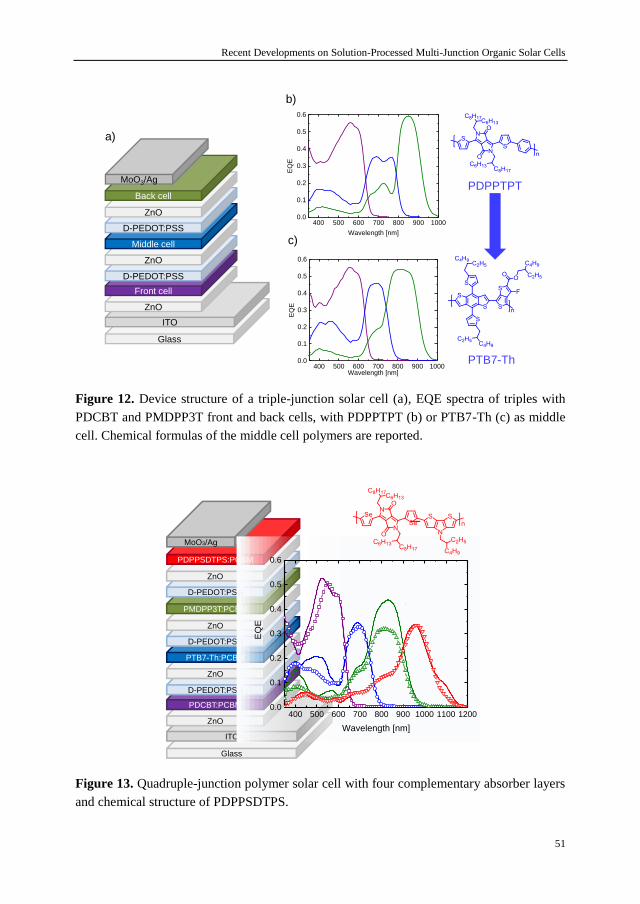
Recent Developments on Solution-Processed Multi-Junction Organic Solar Cells
51
Figure 12. Device structure of a triple-junction solar cell (a), EQE spectra of triples with
PDCBT and PMDPP3T front and back cells, with PDPPTPT (b) or PTB7-Th (c) as middle
cell. Chemical formulas of the middle cell polymers are reported.
Figure 13. Quadruple-junction polymer solar cell with four complementary absorber layers
and chemical structure of PDPPSDTPS.
Glass
ITO
ZnO
Front cell
D-PEDOT:PSS
ZnO
Middle cell
D-PEDOT:PSS
ZnO
Back cell
MoO3/Ag
400 500 600 700 800 900 10000.0
0.1
0.2
0.3
0.4
0.5
0.6
EQ
E
Wavelength [nm]
400 500 600 700 800 900 10000.0
0.1
0.2
0.3
0.4
0.5
0.6
EQ
E
Wavelength [nm]
PDPPTPT
PTB7-Th
a)
b)
c)
Glass
ITO
ZnO
PDCBT:PCBM
D-PEDOT:PSS
ZnO
PTB7-Th:PCBM
D-PEDOT:PSS
ZnO
PMDPP3T:PCBM
D-PEDOT:PSS
ZnO
PDPPSDTPS:PCBM
MoO3/Ag
400 500 600 700 800 900 1000 1100 12000.0
0.1
0.2
0.3
0.4
0.5
0.6
EQ
E
Wavelength [nm]

Chapter 2
52
Table 2. Overview of the relevant data concerning solution-processed organic three- and
four-fold junction solar cells covered by this chapter.
Cell configuration a) Eg b) [eV] VOC [V] Type c) PCE [%] Interconnecting layer
Front|Back Ref
PSEHTT:ICBA (1)
PTB7:PC70BM (2)
PMDPP3T:PC70BM (3)
1.82
1.61
1.30
2.24 3-fold I 11.8
pH-neutral
PEDOT:PSS|LZO sol-
gel/C60-SAM
104
PCDTBT:PC70BM (1)
PMDPP3T:PC60BM (2,3)
1.88
1.30 2.03 3-fold C 6.7
ZnO np|pH-neutral
PEDOT:PSS 105
PBDTTPD:PC70BM (1-3) 1.85 2.75 3-fold C 7.4 ZnO np|Al/MoO3 94
PTB7:PC70BM (1-3) 1.61 2.13 3-fold I 8.7 MoO3/Ag|PFN 106
PCDTBT:PC70BM (1)
PDPPTPT:PC60BM (2)
PDPP5T:PC60BM (3)
1.88
1.53
1.46
2.26 3-fold I 6.0 PEDOT:PSS|ZnO np 40
PDCBT:PC60BM (1)
PDPPTPT:PC70BM (2)
PMDPP3T:PC60BM (3)
1.90
1.53
1.30
2.20 3-fold I 8.7 PEDOT:PSS|ZnO np 40
PDCBT:PC60BM (1)
PTB7-Th:PC70BM (2)
PMDPP3T:PC60BM (3)
1.90
1.58
1.30
2.15 3-fold I 10.0 PEDOT:PSS|ZnO np 40
PDCBT:PC60BM (1)
PTB7-Th:PC70BM (2)
PMDPP3T:PC60BM (3)
PDPPSDTPS:PC60BM (4)
1.90
1.58
1.30
1.13
2.45 4-fold I 7.6 PEDOT:PSS|ZnO np 41
a) The numbers in parentheses refer to the subcell number in the stack, with (1) being the front cell. b) Eg is the
lowest optical band gap of the materials blended in the active layer, with exception of fullerene derivatives, for
which it was omitted. c) C = conventional structure, I = inverted structure.
2.4 Accurate characterization
The OPV community has been actively putting a tremendous effort to increase the
efficiency of solution-processed organic tandem solar cells, as can be argued by reading the
previous sections. For a reliable development of this technology, it is important to carefully
define suitable characterization methods. In this way a fair and accurate mean of comparison
of the different works would be available. These methods should take into account for the
peculiarity of organic tandem solar cells, differentiating them from traditional silicon-based
solar cells. To this end, in 2015 Timmreck et al. analyzed the characterization practices
adopted in literature on OPV tandem cells from January 2009 to September 2014.[107] Their
alarming conclusion was that 51% of the published papers provided no EQE measurement
of the subcells and no comment on the mismatch factor. 45% of the references reported the
EQE measurement for the subcells but provided no comment about the mismatch factor (M)
or they did not use it at all. Only the remaining 4% performed a characterization according
to the standard ASTM E2236. In their correspondence, Timmreck et al. proposed a series of
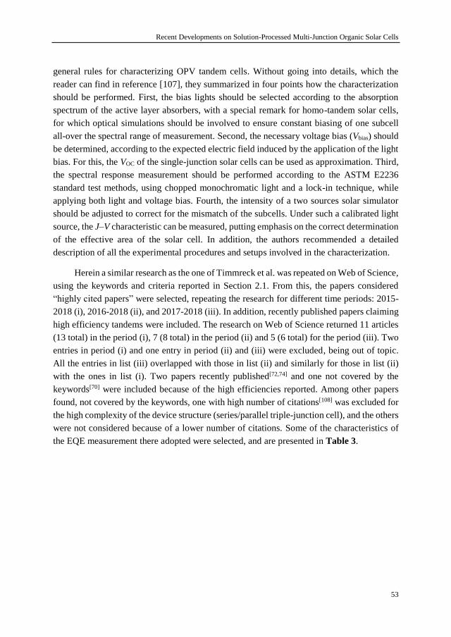
Recent Developments on Solution-Processed Multi-Junction Organic Solar Cells
53
general rules for characterizing OPV tandem cells. Without going into details, which the
reader can find in reference [107], they summarized in four points how the characterization
should be performed. First, the bias lights should be selected according to the absorption
spectrum of the active layer absorbers, with a special remark for homo-tandem solar cells,
for which optical simulations should be involved to ensure constant biasing of one subcell
all-over the spectral range of measurement. Second, the necessary voltage bias (Vbias) should
be determined, according to the expected electric field induced by the application of the light
bias. For this, the VOC of the single-junction solar cells can be used as approximation. Third,
the spectral response measurement should be performed according to the ASTM E2236
standard test methods, using chopped monochromatic light and a lock-in technique, while
applying both light and voltage bias. Fourth, the intensity of a two sources solar simulator
should be adjusted to correct for the mismatch of the subcells. Under such a calibrated light
source, the J–V characteristic can be measured, putting emphasis on the correct determination
of the effective area of the solar cell. In addition, the authors recommended a detailed
description of all the experimental procedures and setups involved in the characterization.
Herein a similar research as the one of Timmreck et al. was repeated on Web of Science,
using the keywords and criteria reported in Section 2.1. From this, the papers considered
“highly cited papers” were selected, repeating the research for different time periods: 2015-
2018 (i), 2016-2018 (ii), and 2017-2018 (iii). In addition, recently published papers claiming
high efficiency tandems were included. The research on Web of Science returned 11 articles
(13 total) in the period (i), 7 (8 total) in the period (ii) and 5 (6 total) for the period (iii). Two
entries in period (i) and one entry in period (ii) and (iii) were excluded, being out of topic.
All the entries in list (iii) overlapped with those in list (ii) and similarly for those in list (ii)
with the ones in list (i). Two papers recently published[72,74] and one not covered by the
keywords[70] were included because of the high efficiencies reported. Among other papers
found, not covered by the keywords, one with high number of citations[108] was excluded for
the high complexity of the device structure (series/parallel triple-junction cell), and the others
were not considered because of a lower number of citations. Some of the characteristics of
the EQE measurement there adopted were selected, and are presented in Table 3.

Chapter 2
54
Table 3. Literature survey on solution-processed multi-junction organic tandem solar cells
in the period: January 2015−August 2018. Please refer to the main text for a detailed
description of the criteria.
EQE
tandem
Light
bias
Vbias δJSCEQE
[%]a)
Ref.
+ b) − − n.a. c) 9
+ b) − − n.a. c) 38
+ + − +2.2 12
+ + − +3.8 55
+ d) + − +4.8 56
+ + − +8.7 57
+ + − +0.7 69
+ + n.m. e) +1.5 70
+ + − +3.8 72
+ + − −0.7 77
+ + − n.a. c) 80
+ d) + f) − +8.3 104
+ + + g) +8.7 10
+ + + +1.1 74
a) Relative deviation of the JSC measured under solar simulator with respect to the JSC from
integration of the EQE spectrum of the current-limiting subcell with the reference AM1.5G
solar spectrum (JSCEQE). b) Homo-tandem. c) JSC
EQE Not available. d) Summed EQE of the
subcells exceeds 100% at some wavelengths. e) Not mentioned. f) No details provided g) No
explanation of the choice.
From this list of sensible publications it appears that researchers gave greater
consideration to the importance of EQE measurement, which was neglected in half of the
published papers before the aforementioned correspondence. Although not always described
in detail, a light bias is provided in all the references in Table 3. Two cases[9,38] where homo-
tandem cells were studied, limit themselves to report the EQE measurement without any bias.
Provided that leakage paths in the subcells do no contribute significantly, this should
correspond to the lower envelope of the EQEs of the two subcells.[107] For what concerns the
application of a voltage bias during the EQE measurement, only reference [10] and [74]
report the use of this correction, necessary to not overestimate the efficiency. Although the
correspondence by Timmreck et al. recommends to put effort in the determination of the
exact effective area, neither of the cited publications in Table 3 mentions this for the EQE
measurement. Reference [55] mentions that the size of the beam of the probe light was
smaller than the cell area. This might affect the accuracy of the measurement, especially
because of the high conductivity of many formulations of PEDOT:PSS, largely used to
fabricate tandems.[109,110,111] The overlap of the area of the bottom and top electrodes defines
the effective area in the dark. When light shines on the sample, the lateral region around this

Recent Developments on Solution-Processed Multi-Junction Organic Solar Cells
55
intersection photogenerates charges which can be collected by a highly conductive interlayer,
leading to overestimation of the real current (the entity depends on the lateral conductivity of
the interlayer(s) in question). In addition, the manufacturing of both semitransparent ITO
electrode and the metal contact are subject to limited accuracy, possibly leading to substantial
deviations in their areas and overlap from the nominal values. Therefore, measuring not only
the J−V characteristic but also the EQE (and also for the calibrated reference cell) through
an opaque, non-reflecting mask with an accurately determined aperture area represents a
good practice to avoid such issue. Only reference [10] and [74] report the mismatch factor of
the subcells and only [74] comments on how it was determined. Given the fact that in a series-
connected tandem solar cell the current is limited by the subcell generating less current, it is
interesting to compare the JSC of the tandem measured under simulated solar radiation
(AM1.5G spectrum) with the JSC of the current-limiting subcell (limJSCEQE). The latter can be
derived from its corresponding EQE spectrum, integrated with the tabulated reference
AM1.5G solar spectrum. In Table 3 the relative deviations between JSC and limJSCEQE is
indicated with δJSCEQE. Another easy operation for a quick check that gives more information
about the EQE measurement consists in adding up the EQEs of the individual subcells.
Although this in not always done in this sample of literature, we note that in references [56]
and [104] the summed EQE locally exceeds 100%. No comment was given on possible
reasons for this remarkable outcome.
The correspondence by Timmreck et al. provided a rigorous method to accurately
determine the efficiency of OPV devices. Possibly due to the limited experimental
availability and/or the intricate nature of some of the steps enumerated, the application of this
vade mecum is never fully rigorously performed (following the sensible sample of the recent
literature here considered). Nevertheless, what discussed in this section about the EQE
measurement can likely improve the accuracy, without introducing experimental
complications. In particular, (1) the usage of the proper voltage bias (or the readily available
VOC of the single-junction cells as approximation), (2) the use of a shadow mask with an
accurately determined aperture area, (3) the comparison of the JSC of the tandem as measured
under simulated solar radiation with the EQE-integrated JSC of the current-limiting subcell,
(4) and adding up the EQEs of the subcells over the spectral range of measurement.
Concerning homo-tandem solar cells, Bahro et al. addressed the problem of measuring
the individual subcells by using an intermediate electrode in the ICL zone.[95] In their study,
they fabricated homo tandems based on PTB7:PC70BM as active layer. A combination of
modified PEDOT:PSS and ZnO nanoparticles was involved as ICL. For the creation of the
intermediate electrode, another formulation of highly conductive PEDOT:PSS was deposited
before the ICL on top of the front cell, and structured laterally to avoid effects due to its high
lateral conductivity. The thickness of the PEDOT:PSS bilayer in the three-terminal device
was controlled to match the one in the reference two-terminal tandem, without the extra
PEDOT:PSS electrode. The authors showed that the ICL based on the extra electrode implied

Chapter 2
56
no difference in the optoelectronic performance of the device. Therefore, the EQE of both
front and back subcells could be directly measured, by simply contacting the intermediate
electrode.
Chapter 4 covers an accurate characterization protocol for triple-junction polymer solar
cells, also published in reference [112]. The triple was the same already presented in Section
2.3 from reference [40], with PDCBT, PTB7-Th and PMDPP3T blended with PCBM as
front, middle, and back subcells, respectively. Besides the measurement of its J−V
characteristic curve, the focus was given on the EQE measurement of each individual subcell.
The latter was isolated and acquired by optically biasing the other two subcells. For the
purpose, high power light-emitting diodes with wavelength (in nm) of 530, 730, and 940 nm
were used, which matched the absorption spectra of the subcells. By performing optical
modeling calculations, the amount of current generated by each subcell under different
(combinations of) light bias was predicted. Due to the partial spectral overlap, this was aimed
at ensuring with enough confidence that only one subcell is current-limiting over the whole
range of wavelengths of the measurement. In this prediction, the different IQEs of the
subcells were taken into account. In addition, the predicted light intensity experienced by the
subcells under light bias was recreated on single-junction cells representative of the subcells
and their J−V characteristic was measured. In this way, the necessary voltage bias correction
was determined for each subcell. Without this correction, the EQE of the subcells was seen
to substantially overestimate the correct EQE. The measured EQEs matched remarkably well
the predicted spectra via opto-electrical modeling, validating the whole procedure.
2.5 Unusual device architectures
Besides the series and parallel connected tandem solar cells, few works presented new
unusual device architectures. In a series connection the VOCs add up and the current is
determined by the current-limiting subcell, while in a parallel connection, the currents add
up and the VOC is close to the lowest one of the two subcells (usually the active layer with
lowest band gap). Both these factors complicate achieving high PCE values. In 2015 Guo et
al. proposed a new concept to alleviate these stringent criteria,[108] by connecting in series
two times the low band gap absorber, therefore adding up their VOCs, and connecting this
homo tandem in parallel to the wide band gap absorber, which has a higher VOC (Figure 14).
Going from the bottom to the top, first the low band gap (1.46 eV) homo tandem was realized,
using PDPP5T-2:PC60BM in the active layers. The ICL of the tandem consisted of zinc
oxide/pH-neutral PEDOT:PSS, which was also used on top of the back cell. Then, silver
nanowires were casted on the PEDOT:PSS film to provide the internal contact for the parallel
connection. The parallel subcell was fabricated starting from zinc oxide nanoparticles on the
silver nanowire layer, followed by the wide band gap top cell of either PCDTBT:PC70BM

Recent Developments on Solution-Processed Multi-Junction Organic Solar Cells
57
(band gap = 1.88 eV) or the commercial OPV12:PC60BM (band gap = 1.73 eV), and
completed by the MoO3/Ag top electrode. The VOCs of the PDPP5T-2 single cell and the
PCDTBT and OPV12 subcells were: 0.56, 0.82 and 0.77 V, respectively. The bottom homo
tandem gave almost twice the VOC of the DPP cell (1.08 V). The series-parallel solar cell
demonstrated VOCs of 0.89 and 0.82 V for the PCDTBT- and the OPV12-based devices,
respectively. In accordance with the expectations, these values are much higher than the VOC
of the DPP single cell and close to the VOC of the wide band gap cells. Moreover, the JSC of
the subcells nicely summed up, as expected. The complete stack returned JSCs of 9.67 and
9.55 mA cm−2, with PCDTBT and OPV12, respectively. In both cases the PCE was 5.4%.
Figure 14. Series/parallel connected triple-junction cell. Device scheme (a) and cross-
sectional transmission electron microscopy image (b), for which the scale bar is 200 nm.
Please referrer to the man text for a description. Reproduced from Ref. 108 under the CC BY
4.0 License. Copyright 2015 Macmillan Publishers Limited.
2.6 Use of multi-junction polymer solar cells for photoelectrochemical
water splitting
In Chapter 1 the concept and working mechanisms of tandem organic solar cells were
introduced. The direct conversion of solar energy into readily available electrical energy is
pushing the development of devices capable of higher power conversion efficiency (PCE).
Another appealing advantage of these devices comes from the possibility to achieve high
VOC, to be used for photoelectrochemical water splitting. The standard potential for water
splitting is E0H2O = 1.23 V, which in practice is further increased to 1.4−1.8 V due to
(a) (b)

Chapter 2
58
overpotentials for oxygen/hydrogen formation at the electrodes. Provided that enough
operating voltage is delivered by the solar cell, there is a direct proportionality between
photocurrent and hydrogen evolution. Assuming 100% Faradaic efficiency, the solar-to-
hydrogen evolution efficiency (ηSTH) follows the relation ηSTH = Jop × E0H2O / Pin, where Jop is
the operating current density delivered by the cell during water splitting. Preferably the cell
and electrode materials are designed in such a way that the cell operates in its maximum
power point, i.e. Jop = Jmax and Vop = Vmax, in which case ηSTH = PCE × (E0H2O / Vop). In 2013
Esiner et al. demonstrated for the first time the possibility of using triple-junction solar cells
for water splitting.[113] In 2015 Esiner et al. used a more efficient triple-junction solar cell for
photoelectrochemical water splitting, comprising PCDTBT:PC70BM as wide band gap front
cell and PMDPP3T:PC60BM as both middle and back cells.[105] The interconnection of the
subcells was realized with ZnO nanoparticles and pH-neutral PEDOT:PSS. The study shed
light on the effect of the nature and surface area of the catalyst connected to a triple-junction
cell on the ηSTH efficiency. In particular, a ηSTH of 5.4% was afforded with RuO2-coated Ti
substrates as catalysts for both hydrogen and oxygen evolution, with a surface area 15 times
the one of the solar cell used. They also fabricated a water splitting device by replacing the
RuO2 catalyst by the earth-abundant Co3O4/NiMoZn catalysts, which yielded a ηSTH of 4.9%.
When the surface area of the catalyst was reduced to ca. 0.7 times the area of the solar cell,
the higher current density in the catalyst caused an increase in overpotential, which shifted
the operating voltage Vop from 1.49 to 1.67 V, i.e. away from the maximum power point of
the solar cell. Consequently, ηSTH decreased to 3.6%. Because the photon flux is distributed
over only two instead of three absorber layers a tandem solar cell can generate a higher
current density than a triple-junction cell at the same optical band gap. Hence, provided that
the required operating voltage can be reached, a tandem cell can give a high ηSTH. In 2016
Esiner et al. reported a wide band gap donor polymer containing a pentacyclic lactam unit,
PTPTIBDT-OD.[96] The optical band gap of this material is 2.04 eV and in combination with
PC70BM as acceptor it can afford a VOC of 0.90 V in a single-junction solar cell. This active
layer was used for both the front and back subcells of a homo-tandem device. To avoid
voltage losses, the ICL was carefully designed using a ZnO/pH-neutral PEDOT:PSS/MoO3
stack, allowing a VOC of 1.74 V. For the water splitting reaction, the authors connected the
solar cell to a RuO2-coated Ti substrate catalytic electrode for oxygen and hydrogen evolution
or a Pt plate catalyst for hydrogen evolution, in a KOH solution. The operating voltage for
water splitting of this system was 1.5 V. In virtue of the high fill factor (FF) of 0.73 for this
tandem, a ηSTH of 4.3% could be achieved, assuming 100% Faradaic efficiency. Also in 2016,
Gao et al. reported a homo-tandem polymer solar cell adopting PBDTTPD as a wide band
gap donor material in combination with PC70BM.[94] This donor material has a band gap of
1.85 eV and can deliver a VOC of 0.92 V in a single-junction device, together with an internal
quantum efficiency (IQE) around 0.9. The homo tandem affords Jop = 5.4 mA cm−2 during
water splitting at Vop = 1.5 V, using an aqueous NaOH solution and platinum and nickel foam
for hydrogen and oxygen evolution electrodes, respectively. The cell thus affords ηSTH of

Recent Developments on Solution-Processed Multi-Junction Organic Solar Cells
59
6.6% when assuming 100% Faradaic efficiency. In the same year Elias et al. presented a
homo-triple junction for water splitting, i.e. using the same absorber in all the three subcells,
PTB7:PC70BM.[106] The structure of this device was inverted, with the successful
MoO3/Ag/PFN stack as ICL. The triple was characterized by a VOC of 2.13 V, which together
with an outstanding FF of 0.76 (certainly considering the number of layers in the stack)
ensured a high value of Jop. A 6% in ηSTH was achieved at neutral pH, by connecting the triple
cell to a cathode of NiMoZn on stainless steel and an anode of RuO2 on glassy carbon. The
choice of the catalysts is particularly valuable since the first one is made of relatively
abundant materials and the second one was manufactured with a minimal content of RuO2.
As already addressed before, polymer blends with non-fullerene acceptors (NFAs) can
provide in general significantly higher VOCs than fullerene-based cells. In 2016 Liu et al.[67]
and in 2017 Chen et al.[38] reported VOCs of 1.97 V and 2.16 V for these two NFA-based
tandem cells, respectively, and demonstrated the evolution of gasses at the catalytic
electrodes (platinum and nickel foam in a NaOH solution).
2.7 Conclusions
The results reported in this chapter point towards a very active research community on
solution-processed multi-junction organic solar cells. The top efficiency for tandems with
polymer:NFA photoactive blends reached the outstanding record PCE of 17.4%, and for
tandems featuring small molecular donors blended with PCBM the highest PCE is 12.5%.
Worth to mention is a remarkable PCE of 15% for hybrid evaporated small molecules (front
cell) and solution-processed (back cell) tandems. Also all-polymer tandem cells underwent a
significant improvement of the performance up to 11.2%, despite a small number of
investigations addressing these cells. Polymer:PCBM-based tandems were reported multiple
times capable of PCE > 11%. The PTB7-Th donor was adopted in many cases of efficient
tandem solar cells, irrespective of whether PCBM and/or NFA acceptors were blended with
it. In addition to the high efficiency, the high VOC (especially of NFA systems) make OPV
tandems suitable for photoelectrochemical water splitting application. From the point of view
of the ICL, PEDOT:PSS and ZnO nanoparticles are still widely used in research, with
interesting developments to improve their processing. A significant focus lied on the use of
conjugated polyelectrolytes charge transport layers in the ICL. Among these, the use of PFN
was reported by multiple groups, especially in the stack: MoO3/Ag/PFN. The latter allowed
achieving high FF values as well as an intriguing solution to tune the optical electric field in
the device, improving the balance of photocurrent in the subcells. The thickness-dependent
performance of single-junction cells, deriving from bimolecular recombination, was tackled
in some papers by adopting the same absorber system in a homo-tandem solar cell,
demonstrating improved absorption of light, accompanied by an increase in efficiency. All
these recent developments might pave the way towards better performing triple-junction solar

Chapter 2
60
cells, which were developed in a very limited number of studies due to their intricate
requirements in terms of current matching and more elaborate processing and
characterization. From the modeling, manufacturing, and characterization aspects, even a
quadruple-junction polymer solar cell with complementary absorber layers was
demonstrated, expanding the previous toolbox. A critical analysis on the procedure to follow
to correctly characterize OPV tandems was presented in the early 2015. So far few relevant
papers followed the guidelines rigorously, but the awareness of correct characterization has
certainly been increased in recent years. In view of the high efficiencies now reported, the
currently available studies stability on upscaling the technology should be continued, to meet
the requirements for industrial manufacturing and reaching the market.

Recent Developments on Solution-Processed Multi-Junction Organic Solar Cells
61
[1] A. Furlan, R. A. J. Janssen, RSC Polym. Chem. Ser. 2016, 17, 310.
[2] Z. Hong, L. Dou, G. Li, Y. Yang, Top. Appl. Phys., 2015, 130, 315.
[3] N. Li, T. Ameri, C. J. Brabec, in Organic Solar Cells, (Ed. Q. Qiao) CRC Press,
Boca Raton, Florida (USA) 2015, Ch. 12, pp 337-377.
[4] O. Adebanjo, B. Vaagensmith, Q. Qiao, J. Mater. Chem. A 2014, 2, 10331.
[5] K. Glaser, A. Puetz, J. Mescher, D. Bahro, A. Colsmann, in Organic
Photovoltaics, 2nd Ed. (Eds. J. C Brabec, U. Scherf, Ullrich, V. Dyakonov) Wiley-
VCH, Weinheim, Germany 2014, Ch. 14, pp 445-463.
[6] J. You, L. Dou, Z. Hong, G. Li, Y. Yang, Prog. Polym. Sci. 2013, 38, 1909.
[7] T. Ameri, N. Li, C. J. Brabec, Energy Environ. Sci. 2013, 6, 2390.
[8] T. Ameri, G. Dennler, C. Lungenschmied, C. J. Brabec, Energy Environ. Sci.
2009, 2, 347.
[9] H. Zhou, Y. Zhang, C.-K. Mai, S. D. Collins, G. C. Bazan, T.-Q. Nguyen, A. J.
Heeger, Adv. Mater. 2015, 27, 1767.
[10] Y. Cui, H. Yao, B. Gao, Y. Qin, S. Zhang, B. Yang, C. He, B. Xu, J. Hou, J. Am.
Chem. Soc. 2017, 139, 7302.
[11] J. Lee, H. Kang, S. Kee, S. H. Lee, S. Y. Jeong, G. Kim, J. Kim, S. Hong, H. Back,
K. Lee, ACS Appl. Mater. Interfaces 2016, 8, 6144.
[12] K. Zhang, K. Gao, R. Xia, Z. Wu, C. Sun, J. Cao, L. Qian, W. Li, S. Liu, F.
Huang, X. Peng, L. Ding, H.-L. Yip, Y. Cao, Adv. Mater. 2016, 28, 4817.
[13] K. Zhang, B. Fan, R. Xia, X. Liu, Z. Hu, H. Gu, S. Liu, H.-L. Yip, L. Ying, F.
Huang, Y. Cao, Adv. Energy Mater. 2018, 8, 1703180.
[14] K. Zhang, R. Xia, B. Fan, X. Liu, Z. Wang, S. Dong, H.-L. Yip, L. Ying, F.
Huang, Y. Cao, Adv. Mater. 2018, DOI:10.1002/adma.201803166.
[15] L. Zuo, C.-Y. Chang, C.-C. Chueh, S. Zhang, H. Li, A. K.-Y. Jen, H. Chen,
Energy Environ. Sci. 2015, 8, 1712.
[16] A. Martínez-Otero, Q. Liu, P. Mantilla-Perez, M. M. Bajo, J. Martorell, J. Mater.
Chem. A 2015, 3, 10681.
[17] S. Lu, X. Guan, X. Li, W. E. I. Sha, F. Xie, H. Liu, J. Wang, F. Huang, W. C. H.
Choy, Adv. Energy Mater. 2015, 5, 1500631.
[18] C.-H. Chou, W. L. Kwan, Z. Hong, L.-M. Chen, Y. Yang, Adv. Mater. 2011, 23,
1282.
[19] D. W. Zhao, L. Ke, Y. Li, S. T. Tan, A. K. K. Kyaw, H. V. Demir, X. W. Sun, D.
L. Carroll, G. Q. Lo, D. L. Kwong, Sol. Energy Mater. Sol. Cells 2011, 95, 921.
[20] T. Becker, S. Trost, A. Behrendt, I. Shutsko, A. Polywka, P. Görrn, P. Reckers, C.
Das, T. Mayer, D. Di Carlo Rasi, K. H. Hendriks, M. M. Wienk, R. A. J. Janssen,
T. Riedl, Adv. Energy Mater. 2018, 8, 1702533.
2.8 References

Chapter 2
62
[21] J. Yang, R. Zhu, Z. Hong, Y. He, A. Kumar, Y. Li, Y. Yang, Adv. Mater. 2011, 23,
3465.
[22] F. Verbakel, S. C. J. Meskers, R. A. J. Janssen, Appl. Phys. Lett. 2006, 89, 102103.
[23] D. Di Carlo Rasi, P. M. J. G. van Thiel, H. Bin, K. H. Hendriks, G. H. L. Heintges,
M. M. Wienk, R. A. J. Janssen, submitted.
[24] A. F. Mitul, L. Mohammad, S. Venkatesan, N. Adhikari, S. Sigdel, Q. Wang, A.
Dubey, D. Khatiwada, Q. Qiao, Nano Energy 2015, 11, 56.
[25] X. Du, O. Lytken, M. S. Killian, J. Cao, T. Stubhan, M. Turbiez, P. Schmuki, H.-
P. Steinrück, L. Ding, R. H. Fink, N. Li, C. J. Brabec, Adv. Energy Mater. 2017, 7,
1601959.
[26] N. Torabi, A. Behjat, M. Shahpari, S. Edalati, J. Nanophotonics 2015, 9, 093049.
[27] S. Lu, X. Guan, X. Li, J. Liu, F. Huang, W. C. H. Choy, Nano Energy 2016, 21,
123.
[28] S.-Y. Chang, Y.-C. Lin, P. Sun, Y.-T. Hsieh, L. Meng, S.-H. Bae, Y.-W. Su, W.
Huang, C. Zhu, G. Li, K.-H. Wei, Y. Yang, Sol. RRL 2017, 1, 1700139.
[29] Z. Shi, H. Liu, L. Xia, Y. Bai, F. Wang, B. Zhang, T. Hayat, A. Alsaedi, Z. Tan,
Chin. J. Chem. 2018, 36, 194.
[30] S. Lu, H. Lin, S. Zhang, J. Hou, W. C. H. Choy, Adv. Energy Mater. 2017, 7,
1701164.
[31] S. Esiner, H. Van Eersel, M. M. Wienk, R. A. J. Janssen, Adv. Mater. 2013, 25,
2932.
[32] C.-Y. Chang, W.-K. Huang, Y.-C. Chang, K.-T. Lee, H.-Y. Siao, Chem. Mater.
2015, 27, 1869.
[33] W. J. da Silva, F. K. Schneider, A. R. bin Mohd Yusoff, J. Jang, Sci. Rep. 2015, 5,
18090.
[34] R. Kang, S. Park, Y. K. Jung, D. C. Lim, M. J. Cha, J. H. Seo, S. Cho, Adv. Energy
Mater. 2018, 8, 1702165.
[35] H. Kang, S. Kee, K. Yu, J. Lee, G. Kim, J. Kim, J.-R. Kim, J. Kong, K. Lee, Adv.
Mater. 2015, 27, 1408.
[36] S. Kim, H. Kang, S. Hong, J. Lee, S. Lee, B. Park, J. Kim, K. Lee, Adv. Funct.
Mater. 2016, 26, 3563.
[37] Q. Wei, T. Nishizawa, K. Tajima, K. Hashimoto Adv. Mater. 2008, 20, 2211.
[38] S. Chen, G. Zhang, J. Liu, H. Yao, J. Zhang, T. Ma, Z. Li, H. Yan, Adv. Mater.
2017, 29, 1604231.
[39] M. Prosa, M. Tessarolo, M. Bolognesi, T. Cramer, Z. Chen, A. Facchetti, B.
Fraboni, M. Seri, G. Ruani, M. Muccini, Adv. Mater. Interfaces 2016, 3, 1600770.
[40] D. Di Carlo Rasi, K. H. Hendriks, G. H. L. Heintges, G. Simone, G. H. Gelinck, V.
S. Gevaerts, R. Andriessen, G. Pirotte, W. Maes, W. Li, M. M. Wienk, R. A. J.
Janssen, Sol. RRL 2018, 2, 1800018.

Recent Developments on Solution-Processed Multi-Junction Organic Solar Cells
63
[41] D. Di Carlo Rasi, K. H. Hendriks, M. M. Wienk, R. A. J. Janssen, Adv. Mater.
2018, doi.org/10.1002/adma.201803836.
[42] Y. Ka, H. Hwang, C. Kim, Sci. Rep. 2017, 7, 1942.
[43] Y. Ka, H. Kim, S. Han, C. Kim, Nanoscale 2018, 10, 12588.
[44] X. Che, Y. Li, Y. Qu, S. R. Forrest, Nat. Energy 2018, 3, 422.
[45] S. Lee, T. E. Kang, D. Han, H. Kim, B. J. Kim, J. Lee, S. Yoo, Sol. Energy Mater.
Sol. Cells 2015, 137, 34.
[46] L. Zuo, J. Yu, X. Shi, F. Lin, W. Tang, A. K.-Y. Jen, Adv. Mater. 2017, 29,
1702547.
[47] P. Mantilla-Perez, A. Martinez-Otero, P. Romero-Gomez, J. Martorell, ACS Appl.
Mater. Interfaces 2015, 7, 18435.
[48] L. Zuo, C.-Y. Chang, C.-C. Chueh, Y. Xu, H. Chen, A. K.-Y. Jen, J. Mater. Chem.
A 2016, 4, 961.
[49] J. A. Mayer, T. Offermans, M. Chrapa, M. Pfannmöller, S. Bals, R. Ferrini, G.
Nisato, Opt. Express 2018, 26, A240.
[50] A. Mertens, J. Mescher, D. Bahro, M. Koppitz, A. Colsmann, Opt. Express 2016,
24, A898.
[51] M. Riede, C. Uhrich, J. Widmer, R. Timmreck, D. Wynands, G. Schwartz, W.-M.
Gnehr, D. Hildebrandt, A. Weiss, J. Hwang, S. Sundarraj, P. Erk, M. Pfeiffer, K.
Leo, Adv. Funct. Mater. 2011, 21, 3019.
[52] B. Luo, Y. Jiang, L. Mao, W. Meng, F. Jiang, Y. Xu, Y. Zhou, J. Mater. Chem. C
2017, 5, 7884.
[53] S.-H. Liao, H.-J. Jhuo, P.-N. Yeh, Y.-S. Cheng, Y.-L. Li, Y.-H. Lee, S. Sharma,
S.-A. Chen, Sci. Rep. 2015, 4, 6813.
[54] Q. Zhang, X. Wan, F. Liu, B. Kan, M. Li, H. Feng, H. Zhang, T. P. Russell, Y.
Chen, Adv. Mater. 2016, 28, 7008.
[55] Y. Ma, S.-C. Chen, Z. Wang, W. Ma, J. Wang, Z. Yin, C. Tang, D. Cai, Q. Zheng,
Nano Energy 2017, 33, 313.
[56] Z. Zheng, S. Zhang, M. Zhang, K. Zhao, L. Ye, Y. Chen, B. Yang, J. Hou, Adv.
Mater. 2015, 27, 1189.
[57] Z. Zheng, S. Zhang, J. Zhang, Y. Qin, W. Li, R. Yu, Z. Wei, J. Hou, Adv. Mater.
2016, 28, 5133.
[58] W. Li, K. H. Hendriks, A. Furlan, W. S. C. Roelofs, M. M. Wienk, R. A. J.
Janssen, J. Am. Chem. Soc. 2013, 135, 18942.
[59] C. Duan, A. Furlan, J. J. van Franeker, R. E. M. Willems, M. M. Wienk, R. A. J.
Janssen, Adv. Mater. 2015, 27, 4461.
[60] B. Guo, X. Guo, W. Li, X. Meng, W. Ma, M. Zhang, Y. Li, J. Mater. Chem. A
2016, 4, 13251.

Chapter 2
64
[61] S. Song, K. Kranthiraja, J. Heo, T. Kim, B. Walker, S.-H. H. Jin, J. Y. Kim, Adv.
Energy Mater. 2017, 7, 1700782.
[62] J. Hou, O. Inganäs, R. H. Friend, F. Gao, Nat. Mater. 2018, 17, 119.
[63] P. Cheng, G. Li, X. Zhan, Y. Yang, Nat. Photonics 2018, 12, 131.
[64] A. Wadsworth, M. Moser, A. Marks, M. S. Little, N. Gasparini, C. J. Brabec, D.
Baran, I. McCulloch, Chem. Soc. Rev. 2018, DOI 10.1039/C7CS00892A.
[65] G. Zhang, J. Zhao, P. C. Y. Chow, K. Jiang, J. Zhang, Z. Zhu, J. Zhang, F. Huang,
H. Yan, Chem. Rev. 2018, 118, 3447.
[66] J. Liu, S. Chen, D. Qian, B. Gautam, G. Yang, J. Zhao, J. Bergqvist, F. Zhang, W.
Ma, H. Ade, O. Inganäs, K. Gundogdu, F. Gao, H. Yan, Nat. Energy 2016, 1,
16089.
[67] W. Liu, S. Li, J. Huang, S. Yang, J. Chen, L. Zuo, M. Shi, X. Zhan, C.-Z. Li, H.
Chen, Adv. Mater. 2016, 28, 9729.
[68] X. Shi, L. Zuo, S. B. Jo, K. Gao, F. Lin, F. Liu, A. K.-Y. Jen, Chem. Mater. 2017,
29, 8369.
[69] Y. Qin, Y. Chen, Y. Cui, S. Zhang, H. Yao, J. Huang, W. Li, Z. Zheng, J. Hou,
Adv. Mater. 2017, 29, 1606340.
[70] Y. Cui, H. Yao, C. Yang, S. Zhang, J. Hou, Acta Polym. Sin. 2018, 2, 223.
[71] Z. Shi, H. Liu, J. Li, F. Wang, Y. Bai, X. Bian, B. Zhang, A. Alsaedi, T. Hayat, Z.
Tan, Sol. Energy Mater. Sol. Cells 2018, 180, 1.
[72] Y. Zhang, B. Kan, Y. Sun, Y. Wang, R. Xia, X. Ke, Y.-Q.-Q. Yi, C. Li, H.-L. Yip,
X. Wan, Y. Cao, Y. Chen, Adv. Mater. 2018, 30, 1707508.
[73] Q. Yue, Z. Zhou, S. Xu, J. Zhang, X. Zhu, J. Mater. Chem. A 2018, 6, 13588.
[74] L. Meng, Y. Zhang, X. Wan, C. Li, X. Zhang, Y. Wang, X. Ke, Z. Xiao, L. Ding,
R. Xia, H.-L. Yip, Y. Cao, Y. Chen, Science 2018, 361, 1094.
[75] J.-H. Kim, J. B. Park, H. Yang, I. H. Jung, S. C. Yoon, D. Kim, D.-H. Hwang,
ACS Appl. Mater. Interfaces 2015, 7, 23866.
[76] Q. Zhang, X. Wan, F. Liu, B. Kan, M. Li, H. Feng, H. Zhang, T. P. Russell, Y.
Chen, Adv. Mater. 2016, 28, 7008.
[77] M. Li, K. Gao, X. Wan, Q. Zhang, B. Kan, R. Xia, F. Liu, X. Yang, H. Feng, W.
Ni, Y. Wang, J. Peng, H. Zhang, Z. Liang, H.-L. Yip, X. Peng, Y. Cao, Y. Chen,
Nat. Photonics 2017, 11, 85.
[78] J. Yuan, J. Gu, G. Shi, J. Sun, H.-Q. Wang, W. Ma, Sci. Rep. 2016, 6, 26459.
[79] J. Yuan, M. J. Ford, Y. Xu, Y. Zhang, G. C. Bazan, W. Ma, Adv. Energy Mater.
2018, 8, 1703291.
[80] N. Li, C. J. Brabec, Energy Environ. Sci. 2015, 8, 2902.
[81] J. Hanisch, T. Wahl, C. D. Wessendorf, E. Ahlswede, J. Mater. Chem. A 2016, 4,
4771.
Recent Developments on Solution-Processed Multi-Junction Organic Solar Cells
65
[82] L. Mao, J. Tong, S. Xiong, F. Jiang, F. Qin, W. Meng, B. Luo, Y. Liu, Z. Li, Y.
Jiang, C. Fuentes-Hernandez, B. Kippelen, Y. Zhou, J. Mater. Chem. A 2017, 5,
3186.
[83] K. Glaser, P. Beu, D. Bahro, C. Sprau, A. Pütz, A. Colsmann, J. Mater. Chem. A
2018, 6, 9257.
[84] D. Angmo, T. R. Andersen, J. J. Bentzen, M. Helgesen, R. R. Søndergaard, M.
Jørgensen, J. E. Carlé, E. Bundgaard, F. C. Krebs, Adv. Funct. Mater. 2015, 25,
4539.
[85] F. Guo, N. Li, V. V. Radmilović, V. R. Radmilović, M. Turbiez, E. Spiecker, K.
Forberich, C. J. Brabec, Energy Environ. Sci. 2015, 8, 1690.
[86] J. Tong, S. Xiong, Z. Li, F. Jiang, L. Mao, W. Meng, Y. Zhou, Appl. Phys. Lett.
2015, 106, 053306.
[87] J. Tong, S. Xiong, Y. Zhou, L. Mao, X. Min, Z. Li, F. Jiang, W. Meng, F. Qin, T.
Liu, R. Ge, C. Fuentes-Hernandez, B. Kippelen, Y. Zhou, Mater. Horiz. 2016, 3,
452.
[88] F. Livi, R. R. Søndergaard, T. R. Andersen, B. Roth, S. Gevorgyan, H. F. Dam, J.
E. Carlé, M. Helgesen, G. D. Spyropoulos, J. Adams, T. Ameri, C. J. Brabec, M.
Legros, N. Lemaitre, S. Berny, O. R. Lozman, S. Schumann, A. Scheel, P. Apilo,
M. Vilkman, E. Bundgaard, F. C. Krebs, Energy Technol. 2015, 3, 423.
[89] J. Adams, G. D. Spyropoulos, M. Salvador, N. Li, S. Strohm, L. Lucera, S.
Langner, F. Machui, H. Zhang, T. Ameri, M. M. Voigt, F. C. Krebs, C. J. Brabec,
Energy Environ. Sci. 2015, 8, 169.
[90] E. B. L. Pedersen, D. Angmo, H. F. Dam, K. T. S. Thydén, T. R. Andersen, E. T.
B. Skjønsfjell, F. C. Krebs, M. Holler, A. Diaz, M. Guizar-Sicairos, D. W. Breiby,
J. W. Andreasen, Nanoscale 2015, 7, 13765.
[91] H. F. Dam, T. R. Andersen, E. B. L. Pedersen, K. T. S. Thydén, M. Helgesen, J. E.
Carlé, P. S. Jørgensen, J. Reinhardt, R. R. Søndergaard, M. Jørgensen, E.
Bundgaard, F. C. Krebs, J. W. Andreasen, Adv. Energy Mater. 2015, 5, 1400736.
[92] T. T. Larsen-Olsen, T. R. Andersen, H. F. Dam, M. Jørgensen, F. C. Krebs, Sol.
Energy Mater. Sol. Cells 2015, 137, 154.
[93] A. R. bin Mohd Yusoff, D. Kim, F. K. Schneider, W. J. da Silva, J. Jang, Energy
Environ. Sci. 2015, 8, 1523.
[94] Y. Gao, V. M. Le Corre, A. Gaïtis, M. Neophytou, M. A. Hamid, K. Takanabe, P.
M. Beaujuge, Adv. Mater. 2016, 28, 3366.
[95] D. Bahro, M. Koppitz, A. Mertens, K. Glaser, J. Mescher, A. Colsmann, Adv.
Energy Mater. 2015, 5, 1501019.
[96] S. Esiner, G. W. P. van Pruissen, M. M. Wienk, R. A. J. Janssen, J. Mater. Chem.
A 2016, 4, 5107.
[97] H. Y. Han, H. Yoon, C. S. Yoon, Sol. Energy Mater. Sol. Cells 2015, 132, 56.

Chapter 2
66
[98] S.-C. Chen, Q. Zheng, Z. Yin, D. Cai, Y. Ma, Org. Electron. 2017, 47, 79.
[99] F. Yang, D.-W. Kang, Y.-S. Kim, Sol. Energy 2017, 155, 552.
[100] F. Yang, D.-W. Kang, Y.-S. Kim, Sol. Energy 2018, 163, 434.
[101] M. Prosa, N. Li, N. Gasparini, M. Bolognesi, M. Seri, M. Muccini, C. J. Brabec,
Adv. Mater. Interfaces 2017, 4, 1700776.
[102] A. Brown, M. Green, Prog. Photovolt: Res. Appl. 2002, 10, 299.
[103] C.-C. Chen, W.-H. Chang, K. Yoshimura, K. Ohya, J. You, J. Gao, Z. Hong, Y.
Yang, Adv. Mater. 2014, 26, 5670.
[104] A. R. bin Mohd Yusoff, D. Kim, H. P. Kim, F. K. Shneider, W. J. da Silva, J. Jang,
Energy Environ. Sci. 2015, 8, 303.
[105] S. Esiner, R. E. M. Willems, A. Furlan, W. Li, M. M. Wienk, R. A. J. Janssen, J.
Mater. Chem. A 2015, 3, 23936.
[106] X. Elias, Q. Liu, C. Gimbert-Suriñach, R. Matheu, P. Mantilla-Perez, A. Martinez-
Otero, X. Sala, J. Martorell, A. Llobet, ACS Catal. 2016, 6, 3310.
[107] R. Timmreck, T. Meyer, J. Gilot, H. Seifert, T. Mueller, A. Furlan, M. M. Wienk,
D. Wynands, J. Hohl-Ebinger, W. Warta, R. A. J. Janssen, M. Riede, K. Leo, Nat.
Photonics 2015, 9, 478.
[108] F. Guo, N. Li, F. W. Fecher, N. Gasparini, C. O. R. Quiroz, C. Bronnbauer, Y.
Hou, V. V. Radmilović, V. R. Radmilović, E. Spiecker, K. Forberich, C. J. Brabec,
Nat. Commun. 2015, 6, 7730.
[109] A. Cravino, P. Schilinsky, C. J. Brabec, Adv. Funct. Mater. 2007, 17, 3906.
[110] M.-S. Kim, M.-G. Kang, L. J. Guo, J. Kim, Appl. Phys. Lett. 2008, 92, 133301.
[111] S. Sista, M.-H. Park, Z. Hong, Y. Wu, J. Hou, W. L. Kwan, G. Li, Y. Yang, Adv.
Mater. 2010, 22, 380.
[112] D. Di Carlo Rasi, K. H. Hendriks, M. M. Wienk, R. A. J. Janssen, Adv. Energy
Mater. 2017, 7, 1701664.
[113] S. Esiner, H. Van Eersel, M. M. Wienk, R. A. J. Janssen, Adv. Mater. 2013, 25,
2932.

Chapter 3
A Universal Route to Fabricate n-i-p Multi-
Junction Polymer Solar Cells via Solution
Processing*
Abstract
The interconnection layer (ICL) that connects adjacent subcells electrically and
optically in solution-processed multi-junction polymer solar cells must meet functional
requirements in terms of work functions, conductivity, and transparency, but also be
compatible with the multiple layer stack in terms of processing and deposition conditions.
Using a combination of poly(3,4-ethylenedioxythiophene):polystyrene sulfonate, diluted in
near azeotropic water/n-propanol dispersions as hole transport layer, and ZnO
nanoparticles, dispersed in isoamyl alcohol as electron transport layer, a novel, versatile
ICL has been developed for solution-processed tandem and triple-junction solar cells in an
n-i-p architecture. The ICL has been incorporated in six different tandem cells and three
different triple-junction solar cells, employing a range of different polymer-fullerene
photoactive layers. The new ICL provided an essentially lossless contact in each case,
without the need of adjusting the formulations or deposition conditions. The approach
permitted realizing complex devices in good yields, providing a power conversion efficiency
up to 10%.
* This chapter has been published as: D. Di Carlo Rasi, K. H. Hendriks, G. H. L. Heintges,
G. Simone, G. H. Gelinck, V. S. Gevaerts, R. Andriessen, G. Pirotte, W. Maes, W. Li, M.
M. Wienk, R. A. J. Janssen, Sol. RRL 2018, 2, 1800018.

Chapter 3
68
3.1 Introduction
The main challenge in developing a procedure for making multi-junction solar cells
from solution is the fabrication of the interconnecting layer (ICL). The ICL is composed of
charge-selective interlayer materials that ensure the recombination of opposite charges from
two adjacent active layers, without energy loss. This is done by stacking an electron transport
material and a hole transport material (Chapter 1). Efficient, solution-processable ICLs
should satisfy a number of requirements:
(1) The Fermi levels of the ICL must match with the relevant highest occupied
molecular orbital (HOMO) and lowest unoccupied molecular orbital LUMO energy
levels of the organic materials in the adjacent active layers that are sandwiching the
ICL to create Ohmic contacts.
(2) The materials in the ICL should possess sufficient Ohmic conductance to enable fast
recombination of charges and to avoid loss of potential energy or fill factor.
(3) The parasitic absorption of sunlight should be low.
(4) The temperatures at which the processing and any post-treatment are performed
should not deteriorate the performance of the active layers in the device.
(5) The formulation of the solutions from which the ICL is cast should not interfere
with the underlying materials in the sequence of the device stack.
(6) The ICL should prevent that the solvents that are used to deposit subsequent layers
in the stack, penetrate and dissolve underlying layers.
(7) The processing of the ICL should be versatile, so that it can be used for many
combinations of active layers from different materials.
In recent years, several different combinations of materials have been proposed as ICL,
involving either organic materials or transparent semiconducting metal oxides[1-15] (refer also
to Chapter 2). For the selective extraction of holes from the photoactive layers poly(3,4-
ethylenedioxythiophene):polystyrene sulfonate (PEDOT:PSS) is widely used but also metal
oxides such as MoO3,[16] V2O5,[17] and WO3,[18] or graphene oxide (GO)[19] can be used for
the purpose. For selective electron extraction, solution-processed metal oxides such as ZnO
nanoparticles,[20] sol-gel TiO2,[1] or Li-doped ZnO[21] are popular. These metal oxides can be
covered by self-assembled monolayers[22] or poly[(9,9-bis(3'-(N,N-dimethylamion)propyl)-
2,7-fluorene)-alt-2,7-(9,9-dioctyl)-fluorene] (PFN)[23] to improve charge selectivity. Also
polyamines such as ethoxylated polyethylenimine (PEIE)[24] and polyethylenimine (PEI)[25]
have been used to modify the work function of PEDOT:PSS or metal oxides to create an
effective low work function, electron selective contact. One of the reasons for the large
A Universal Route to Fabricate n-i-p Multi-Junction Polymer Solar Cells via Solution Processing
69
variety of ICLs stems from the fact that the proposed materials or their processing conditions
are often quite specific to the nature of the photoactive layers. A universal, solution-based
method that works in combination with a large number of different active layers does not
exist at present. The choice of ICL and the details of its casting conditions (mainly the
formulation of the solutions) do vary substantially according to the particular stack of
materials under consideration, to ensure the so-called orthogonality of casting solvents
(related to requirements (5) and (6) above). The match of the surface energy of the inks from
which we process the ICL to the surface energy of the organic active layer plays a major role
in the formation of the film.[26] Regarding requirement (4), we note that for some of the
materials used in this work even mild temperatures like 60 °C decrease the photovoltaic
performance of the photoactive layer, probably due to morphology changes. Hence, a
universal route to fabricate multi-junction polymer solar cells via solution processing at mild
temperatures is in great demand.
Herein, we describe a combination of interlayers and processing conditions that fulfill
the entire list of requirements. We developed new formulations for dispersions of
PEDOT:PSS and ZnO nanoparticles in solvents that enable orthogonal processing of the ICL
on any photoactive layer in an inverted (n-i-p) configuration we have tested. The reasons to
choose for PEDOT:PSS and ZnO are their favorable work functions, and room temperature
deposition conditions from benign solvents. To demonstrate this, we combined photoactive
layers based on polymer-fullerene blends of different nature to fabricate six tandem and three
triple-junction solar cells. A total of eight different active layers were tested in varying
configurations, as front or back subcells in tandems, or as a middle subcell in triple junctions.
The performance characteristics of these multi-junction devices were, in general, in good
agreement with the expected performance based on the properties of corresponding single-
junction devices. As proof of concept, triple-junction solar cells with a power conversion
efficiency of 10% were realized with excellent statistical relevance (yield 94%).
3.2 Results and Discussion
3.2.1 Materials and device architectures
To develop a versatile method for coating the ICL in different device stacks we decided
to develop and test ICL formulations on active layer materials of different chemical nature
and with different opto-electrical properties, suitable for different roles in tandem and triple-
junction cells. We adopted an inverted (n-i-p) device configuration in which the electron
transporting layer (ETL) is deposited first, followed by the active layer and the hole transport
layer (HTL). There are several reasons to prefer an inverted (n-i-p) over a conventional (p-i-
n) device architecture, mainly related to the use of PEDOT:PSS as HTL. In the conventional
structure, the HTL is positioned between the light source and the photoactive layer, which

Chapter 3
70
leads to parasitic absorption by the polaron/bipolaron absorption bands of PEDOT:PSS in
the near infrared.[27] Further, the acidic nature of the commercial PEDOT:PSS dispersions in
water causes that it cannot be deposited on ZnO without deteriorating this layer or even
washing it away completely. Increasing the pH of the dispersion can mitigate this, but lowers
the work function of the resulting PEDOT:PSS layer. In turn this limits the open-circuit
voltage (VOC) that can be reached and necessitates the use of additional MoO3 or Nafion
layers to compensate for this loss.[ 28 ] Reversing the processing order of the ZnO and
PEDOT:PSS layers avoids these complications. Finally, the Ag back electrode that is
commonly used in the n-i-p configuration is more reflective than the Al back contact in most
p-i-n structures.[ 29] The general sequence of layers in single, double and triple-junction
devices used in this work is shown in Figure 1.
Figure 1. Device architecture of n-i-p (a) single, (b), double, and (c) triple-junction solar
cells adopted in this work.
The optimal position of an organic semiconductor layer in a multi-junction stack is
dictated by its optical band gap: wide band gap materials are preferably close to the
Glass
ITO
ZnO
Front cell
PEDOT:PSS
ETL
Back cell
MoO3/Ag
Glass
ITO
ZnO
Front cell
PEDOT:PSS
ETL
Middle cell
PEDOT:PSS
ETL
Back cell
MoO3/Ag
Glass
ITO
ZnO
Active layer
MoO3/Ag
(a)
(b)
(c)

A Universal Route to Fabricate n-i-p Multi-Junction Polymer Solar Cells via Solution Processing
71
transparent electrode (front subcell), while low band gap materials are close to the reflecting
back contact (back subcell). This generally represents an optimal choice because the high
energy of photons from the blue part of the solar spectrum would be lost by thermalization if
these were absorbed by the low band gap material. Materials with an intermediate band gap
can be conveniently used in various positions, especially as middle cell in triple-junction
solar cells.
Figure 2 and Table 1 show the donor polymers tested in this study. We used PCDTBT
(Eg = 1.88 eV), PBDTTPD (Eg = 1.85 eV), and PDCBT (Eg = 1.90 eV) as wide band gap
donors in the front subcells.[30,31,32] For the back subcells we selected PDPP5T (Eg = 1.46 eV),
PDPP3T (Eg = 1.33 eV), and its methylated version PMDPP3T (Eg = 1.30 eV) as
donors.[4,33 ,34] Donors that were used either in the front, middle, or back subcells were
PDPPTPT (Eg = 1.53 eV) and PTB7-Th (Eg = 1.58 eV).[35,36] All donors were used in
combination with [6,6]-phenyl-C61-butyric acid methyl ester (PC60BM) or [6,6]-phenyl-C71-
butyric acid methyl ester (PC70BM).
Table 1. Systematic names of the donor polymers used.
PCDTBT poly[N-9″-heptadecanyl-2,7-carbazole-alt-5,5-(4′,7′-di-2-thienyl-2′,1′,3′-
benzothiadiazole)])
PBDTTPD poly[bis(2'-ethylhexyloxy)benzo[1,2-b:4,5-b’]dithiophene-alt-N-
octylthieno[3,4-c]pyrrole-4,6-dione]
PDCBT poly[5,5′-bis(2-butyloctyl)-(2,2′-bithiophene)-4,4′-dicarboxylate-alt-5,5′-
2,2′-bithiophene]
PDPP5T poly[[2,5-bis(2-hexyldecyl)-2,3,5,6-tetrahydro-3,6-dioxopyrrolo[3,4-c]
pyrrole-1,4-diyl]-alt-(3''',4'-dihexyl[2,2':5',2'':5'',2''':5''',2''''-
quinquethiophene]-5,5''''-diyl)]
PDPP3T poly[[2,5-bis(2-hexyldecyl)-2,3,5,6-tetrahydro-3,6-dioxopyrrolo[3,4-
c]pyrrole-1,4-diyl]-alt-[2,2′:5′,2″-terthiophene]-5,5″-diyl]
PMDPP3T poly[[2,5-bis(2-hexyldecyl)-2,3,5,6-tetrahydro-3,6-dioxopyrrolo[3,4-
c]pyrrole-1,4-diyl]-alt-[3′,3″-dimethyl-2,2′:5′,2″-terthiophene]-5,5″-diyl]
PDPPTPT poly[{2,5-bis(2-hexyldecyl)-2,3,5,6-tetrahydro-3,6-dioxopyrrolo[3,4-
c]pyrrole-1,4-diyl}-alt-{[2,2′-(1,4-phenylene)bisthiophene]-5,5′-diyl}]
PTB7-Th poly[4,8-bis(5-(2-ethylhexyl)thiophen-2-yl)benzo[1,2-b:4,5-
b′]dithiophene-co-3-fluorothieno[3,4-b]thiophene-2-carboxylate]
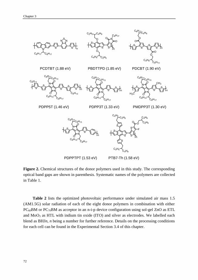
Chapter 3
72
Figure 2. Chemical structures of the donor polymers used in this study. The corresponding
optical band gaps are shown in parenthesis. Systematic names of the polymers are collected
in Table 1.
Table 2 lists the optimized photovoltaic performance under simulated air mass 1.5
(AM1.5G) solar radiation of each of the eight donor polymers in combination with either
PC60BM or PC70BM as acceptor in an n-i-p device configuration using sol-gel ZnO as ETL
and MoO3 as HTL with indium tin oxide (ITO) and silver as electrodes. We labelled each
blend as BHJn, n being a number for further reference. Details on the processing conditions
for each cell can be found in the Experimental Section 3.4 of this chapter.
PDCBT (1.90 eV)
PTB7-Th (1.58 eV)
PMDPP3T (1.30 eV)
PBDTTPD (1.85 eV)
PDPP3T (1.33 eV)PDPP5T (1.46 eV)
PDPPTPT (1.53 eV)
PCDTBT (1.88 eV)
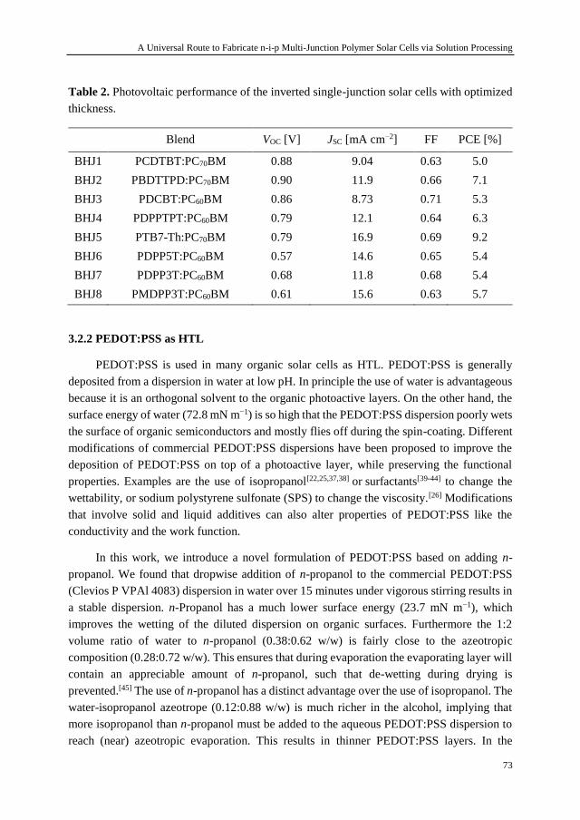
A Universal Route to Fabricate n-i-p Multi-Junction Polymer Solar Cells via Solution Processing
73
Table 2. Photovoltaic performance of the inverted single-junction solar cells with optimized
thickness.
Blend VOC [V] JSC [mA cm−2] FF PCE [%]
BHJ1 PCDTBT:PC70BM 0.88 9.04 0.63 5.0
BHJ2 PBDTTPD:PC70BM 0.90 11.9 0.66 7.1
BHJ3 PDCBT:PC60BM 0.86 8.73 0.71 5.3
BHJ4 PDPPTPT:PC60BM 0.79 12.1 0.64 6.3
BHJ5 PTB7-Th:PC70BM 0.79 16.9 0.69 9.2
BHJ6 PDPP5T:PC60BM 0.57 14.6 0.65 5.4
BHJ7 PDPP3T:PC60BM 0.68 11.8 0.68 5.4
BHJ8 PMDPP3T:PC60BM 0.61 15.6 0.63 5.7
3.2.2 PEDOT:PSS as HTL
PEDOT:PSS is used in many organic solar cells as HTL. PEDOT:PSS is generally
deposited from a dispersion in water at low pH. In principle the use of water is advantageous
because it is an orthogonal solvent to the organic photoactive layers. On the other hand, the
surface energy of water (72.8 mN m−1) is so high that the PEDOT:PSS dispersion poorly wets
the surface of organic semiconductors and mostly flies off during the spin-coating. Different
modifications of commercial PEDOT:PSS dispersions have been proposed to improve the
deposition of PEDOT:PSS on top of a photoactive layer, while preserving the functional
properties. Examples are the use of isopropanol[22,25,37,38] or surfactants[39-44] to change the
wettability, or sodium polystyrene sulfonate (SPS) to change the viscosity.[26] Modifications
that involve solid and liquid additives can also alter properties of PEDOT:PSS like the
conductivity and the work function.
In this work, we introduce a novel formulation of PEDOT:PSS based on adding n-
propanol. We found that dropwise addition of n-propanol to the commercial PEDOT:PSS
(Clevios P VPAl 4083) dispersion in water over 15 minutes under vigorous stirring results in
a stable dispersion. n-Propanol has a much lower surface energy (23.7 mN m−1), which
improves the wetting of the diluted dispersion on organic surfaces. Furthermore the 1:2
volume ratio of water to n-propanol (0.38:0.62 w/w) is fairly close to the azeotropic
composition (0.28:0.72 w/w). This ensures that during evaporation the evaporating layer will
contain an appreciable amount of n-propanol, such that de-wetting during drying is
prevented.[45] The use of n-propanol has a distinct advantage over the use of isopropanol. The
water-isopropanol azeotrope (0.12:0.88 w/w) is much richer in the alcohol, implying that
more isopropanol than n-propanol must be added to the aqueous PEDOT:PSS dispersion to
reach (near) azeotropic evaporation. This results in thinner PEDOT:PSS layers. In the

Chapter 3
74
following we refer to this new formulation as D-PEDOT:PSS (diluted in n-propanol). We
remark that n-propanol evaporates virtually completely during spin-coating, leaving nothing
more than just PEDOT:PSS in the layer.
We optimized the amount of n-propanol that is necessary to uniformly cover the active
layer. Figure 3 shows pictures taken with a camera of three different bulk-heterojunction
layers, before and after spin-coating of D-PEDOT:PSS on top. For the deposition we used
spin-coating at 500 rpm in a nitrogen filled glove box, which was found to improve the
wetting. Figure 3 shows that dilution of PEDOT:PSS with n-propanol improved the film
formation properties. On a PCDTBT:PC70BM layer, a ratio of water/n-propanol 1:1 (v/v)
seemed sufficient to form a uniform film of PEDOT:PSS on top. For PDPPTPT:PC60BM and
PDPP5T:PC60BM, however, the PEDOT:PSS 1:1 (v/v) diluted dispersion in water/n-
propanol only partially covered the surface, possibly due to a larger difference in surface
energy of these substrates. By further diluting to 1:2 (v/v), the coverage turned uniform for
each of the cases considered. The same 1:2 (v/v) formulation turned out to deposit well on
many other active layers. As explained, the 1:2 mixture corresponds to a mass fraction of n-
propanol of 0.62, close to the azeotropic composition of 0.72. Hence in the last stages of the
drying process, mostly water is present in the layer, which is the native medium of
PEDOT:PSS, but the viscosity at this point has increased because of the increased
PEDOT:PSS concentration such that dewetting or material flying off from the substrate does
not occur. After spin-coating the D-PEDOT:PSS layers were kept in a vacuum of ~10−2 mbar
for 30 minutes to remove residual solvents, and no further treatment was performed.
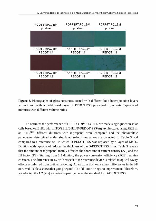
A Universal Route to Fabricate n-i-p Multi-Junction Polymer Solar Cells via Solution Processing
75
Figure 3. Photographs of glass substrates coated with different bulk-heterojunction layers
without and with an additional layer of PEDOT:PSS processed from water/n-propanol
mixtures with different volume ratios.
To optimize the performance of D-PEDOT:PSS as HTL, we made single-junction solar
cells based on BHJ1 with a ITO/PEIE/BHJ1/D-PEDOT:PSS/Ag architecture, using PEIE as
an ETL.[46] Different dilutions with n-propanol were compared and the photovoltaic
parameters determined under simulated solar illumination are collected in Table 3 and
compared to a reference cell in which D-PEDOT:PSS was replaced by a layer of MoO3.
Dilution with n-propanol reduces the thickness of the D-PEDOT:PSS films. Table 3 reveals
that the amount of n-propanol mainly affected the short-circuit current density (JSC) and the
fill factor (FF). Starting from 1:2 dilution, the power conversion efficiency (PCE) remains
constant. The difference in JSC with respect to the reference device is related to optical cavity
effects as inferred from optical modeling. Apart from this, only minor differences in the FF
occurred. Table 3 shows that going beyond 1:2 of dilution brings no improvement. Therefore,
we adopted the 1:2 (v/v) water/n-propanol ratio as the standard for D-PEDOT:PSS.

Chapter 3
76
Table 3. Photovoltaic parameters of ITO/PEIE/PCDTBT:PC70BM/D-PEDOT:PSS/Ag solar
cells with a PEDOT:PSS layer processed from different water/n-propanol (v/v) dispersions.
PEDOT:PSS:n-propanol VOC [V] JSC [mA cm−2] FF PCE [%]
Reference a) 0.87 8.2 0.56 4.0
1:1 (70 nm) 0.86 6.1 0.61 3.2
1:2 (40 nm) 0.89 7.2 0.61 3.9
1:3 (30 nm) 0.88 7.8 0.57 3.9
1:4 (25 nm) 0.87 7.8 0.58 3.9
1:5 (20 nm) 0.88 7.8 0.57 3.8 a) ITO/PEIE/PCDTBT:PC70BM/MoO3/Ag.
3.2.3 PEIE and ZnO nanoparticles as ETL
To create an ICL for tandem solar cells the optimized D-PEDOT:PSS layer must be
combined with an ETL (Figure 1). We decided to test both PEIE and ZnO nanoparticles on
top of the D-PEDOT:PSS film. The function of PEIE is to create a thin (< 10 nm) layer in
which the presence of dipoles or ions at the interface lowers the work function of
PEDOT:PSS, permitting the tunneling of electrons.[46] PEIE is commercially available as an
aqueous solution, but water is not a suitable solvent for processing on top of PEDOT:PSS
layers. Following the procedure of Lee et al. [25] for the non-ethoxylated version of
polyethylenimine (PEI), we diluted PEIE with a significant amount of isopropanol (IPA) to
reach concentrations in IPA around 0.2 wt%. By doing so the content in water reduced to a
marginal amount (in the same order of magnitude as PEIE), avoiding the dissolution of the
PEDOT:PSS layer. PEIE is an insulating material and therefore an optimal coverage of the
substrates is required in order to have correctly working devices. Figure 4 shows how the
J−V characteristics of ITO/D-PEDOT:PSS/PEIE/BHJ7/MoO3/Ag single-junction devices
change in relation to the concentration of PEIE in IPA. If the concentration is too low, the
layer is too thin and, eventually, discontinuous, leading to a reduced FF. On the opposite, a
too high concentration yields a too thick layer, which hinders tunneling of electrons and
creates a barrier at this interface resulting in a lower Jsc and FF. At 0.2 wt% PEIE in IPA the
device performance of the ITO/D-PEDOT:PSS/PEIE/BHJ7/MoO3/Ag cells is very similar to
that of the reference ITO/ZnO/BHJ7/MoO3/Ag cell (Figure 4).
The ZnO nanoparticles were synthesized according to the procedure described in detail
in the Experimental Section 3.4 of this chapter and were re-dispersed in isoamyl alcohol.
Spin-coating the ZnO nanoparticles from isoamyl alcohol on top of a PEDOT:PSS layer is
straightforward.

A Universal Route to Fabricate n-i-p Multi-Junction Polymer Solar Cells via Solution Processing
77
-0.1 0.0 0.1 0.2 0.3 0.4 0.5 0.6 0.7-14
-12
-10
-8
-6
-4
-2
0
2
Curr
ent den
sity [m
A c
m-2]
Voltage [V]
0.1 wt.%
0.2 wt.%
0.4 wt.%
reference
Figure 4. J−V characteristics of ITO/D-PEDOT:PSS/PEIE/BHJ7/MoO3/Ag fabricated using
different concentrations of PEIE in IPA in wt.%. The reference device with sol-gel ZnO on
ITO instead of D-PEDOT:PSS/PEIE is shown for a comparison.
3.2.4 Tandem solar cells
The combination of D-PEDOT:PSS and PEIE or ZnO was used to realize a series of
tandem solar cells featuring different active layer materials (Table 4). Given the complexity
of a full thickness optimization of all layers, we used the optimum thickness of the
photoactive layers of the single-junction cells. By doing so it was still possible to evaluate
the quality of the ICL by checking the addition of the VOC’s of the subcells. Also the FF of
the tandem is determined by the J−V characteristics of both the subcells, and can be found
from the mathematical sum of the J−V curves along the voltage axis, i.e. at constant current
density. In practice the FF of the tandem cell is comparable to that of the current-limiting
subcell. If the processing of the complete stack would degrade any of the layers, it would
unavoidably lower the FF of the tandem cell.
The experimental VOC’s generally agree within a few tens of mV with the value
calculated from the sum of the corresponding single-junction devices (VOCsum). Only for the
two tandem cells featuring BHJ3 (PDCBT:PC60BM) in the front cell a substantial loss in VOC
was found. In general a 10 to 20 mV loss can be expected because the effective light intensity
in each of the subcells of a tandem is less than in a single-junction cell under AM1.5G
illumination. This expected loss can be estimated using ΔVOC =
(kT/q)ln[JSC(tandem)/JSC(single)], i.e. assuming that the ideality factor of diode is unity.
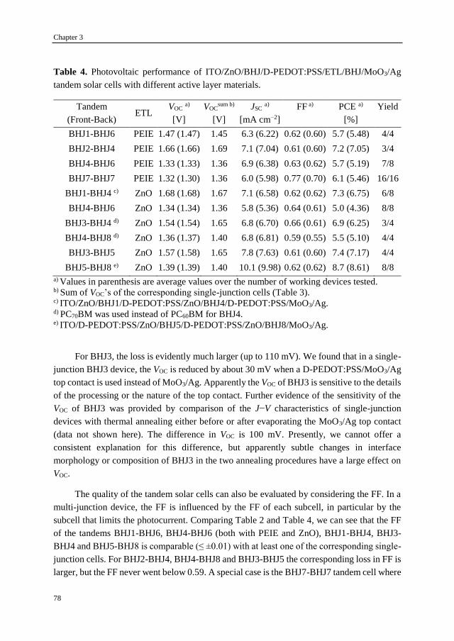
Chapter 3
78
Table 4. Photovoltaic performance of ITO/ZnO/BHJ/D-PEDOT:PSS/ETL/BHJ/MoO3/Ag
tandem solar cells with different active layer materials.
Tandem
(Front-Back) ETL
VOC a)
[V]
VOCsum b)
[V]
JSC a)
[mA cm−2]
FF a)
PCE a)
[%]
Yield
BHJ1-BHJ6 PEIE 1.47 (1.47) 1.45 6.3 (6.22) 0.62 (0.60) 5.7 (5.48) 4/4
BHJ2-BHJ4 PEIE 1.66 (1.66) 1.69 7.1 (7.04) 0.61 (0.60) 7.2 (7.05) 3/4
BHJ4-BHJ6 PEIE 1.33 (1.33) 1.36 6.9 (6.38) 0.63 (0.62) 5.7 (5.19) 7/8
BHJ7-BHJ7 PEIE 1.32 (1.30) 1.36 6.0 (5.98) 0.77 (0.70) 6.1 (5.46) 16/16
BHJ1-BHJ4 c) ZnO 1.68 (1.68) 1.67 7.1 (6.58) 0.62 (0.62) 7.3 (6.75) 6/8
BHJ4-BHJ6 ZnO 1.34 (1.34) 1.36 5.8 (5.36) 0.64 (0.61) 5.0 (4.36) 8/8
BHJ3-BHJ4 d) ZnO 1.54 (1.54) 1.65 6.8 (6.70) 0.66 (0.61) 6.9 (6.25) 3/4
BHJ4-BHJ8 d) ZnO 1.36 (1.37) 1.40 6.8 (6.81) 0.59 (0.55) 5.5 (5.10) 4/4
BHJ3-BHJ5 ZnO 1.57 (1.58) 1.65 7.8 (7.63) 0.61 (0.60) 7.4 (7.17) 4/4
BHJ5-BHJ8 e) ZnO 1.39 (1.39) 1.40 10.1 (9.98) 0.62 (0.62) 8.7 (8.61) 8/8
a) Values in parenthesis are average values over the number of working devices tested. b) Sum of VOC’s of the corresponding single-junction cells (Table 3). c) ITO/ZnO/BHJ1/D-PEDOT:PSS/ZnO/BHJ4/D-PEDOT:PSS/MoO3/Ag. d) PC70BM was used instead of PC60BM for BHJ4. e) ITO/D-PEDOT:PSS/ZnO/BHJ5/D-PEDOT:PSS/ZnO/BHJ8/MoO3/Ag.
For BHJ3, the loss is evidently much larger (up to 110 mV). We found that in a single-
junction BHJ3 device, the VOC is reduced by about 30 mV when a D-PEDOT:PSS/MoO3/Ag
top contact is used instead of MoO3/Ag. Apparently the VOC of BHJ3 is sensitive to the details
of the processing or the nature of the top contact. Further evidence of the sensitivity of the
VOC of BHJ3 was provided by comparison of the J−V characteristics of single-junction
devices with thermal annealing either before or after evaporating the MoO3/Ag top contact
(data not shown here). The difference in VOC is 100 mV. Presently, we cannot offer a
consistent explanation for this difference, but apparently subtle changes in interface
morphology or composition of BHJ3 in the two annealing procedures have a large effect on
VOC.
The quality of the tandem solar cells can also be evaluated by considering the FF. In a
multi-junction device, the FF is influenced by the FF of each subcell, in particular by the
subcell that limits the photocurrent. Comparing Table 2 and Table 4, we can see that the FF
of the tandems BHJ1-BHJ6, BHJ4-BHJ6 (both with PEIE and ZnO), BHJ1-BHJ4, BHJ3-
BHJ4 and BHJ5-BHJ8 is comparable (≤ ±0.01) with at least one of the corresponding single-
junction cells. For BHJ2-BHJ4, BHJ4-BHJ8 and BHJ3-BHJ5 the corresponding loss in FF is
larger, but the FF never went below 0.59. A special case is the BHJ7-BHJ7 tandem cell where

A Universal Route to Fabricate n-i-p Multi-Junction Polymer Solar Cells via Solution Processing
79
the FF (0.77) was significantly higher than for the single-junction cell (0.68). A possible
cause is the reduced light intensity experienced by each subcell (e.g. lower bimolecular
recombination).
Measuring the external quantum efficiency (EQE) spectrum of a tandem cell gives
insight in the current generated by each subcell, but also in the structural integrity of the
layers, especially on the presence of current leakage paths in one or more photoactive layers.
In an ideal tandem cell, the EQE measured without bias light should follow the lower
envelope of the EQEs of the subcells, determined using representative bias light.[47] In case
of a leakage, the EQE without bias light can be substantially higher.[47] Figure 5 shows that
the EQEs of BHJ2-BHJ4 (best tandem with PEIE as ETL) and BHJ5-BHJ8 (best tandem with
ZnO as ETL) measured without light bias are very close to the expected behavior.
By comparison of VOC and FF values and measuring EQE, we conclude that the D-
PEDOT:PSS/PEIE and D-PEDOT:PSS/ZnO ICLs are suitable for use in a range of tandem
cell configurations.
300 400 500 600 700 800 900 1000 11000.0
0.1
0.2
0.3
0.4
0.5
0.6
0.7
EQ
E
Wavelength [nm]
No bias light
Front cell
Back cell
(a)
300 400 500 600 700 800 900 1000 11000.0
0.1
0.2
0.3
0.4
0.5
0.6
0.7
EQ
E
Wavelength [nm]
No bias light
Front cell
Back cell
(b)
Figure 5. EQE spectra of (a) BHJ2-BHJ4 (PEIE as ETL) and (b) BHJ5-BHJ8 (ZnO as ETL)
recorded with (solid lines) and without (dashed lines) bias light; for the nomenclature refer
to Table 1. LED sources (530 and 730 nm (a) or 530 and 940 nm (b)) were used to optically
bias the front and back subcells, respectively.
3.2.5 ICL for triple-junction solar cells: need for second order orthogonality
After demonstrating tandem solar cells using D-PEDOT:PSS/PEIE and D-
PEDOT:PSS/ZnO as ICL, we studied the application of the same layers to fabricate triple-
junction cells. To make triple-junction cells, the ICL must withstand the deposition of a BHJ

Chapter 3
80
as well as a subsequent ICL. To test the compatibility of the layers with the solvents necessary
for processing, we made ITO/D-PEDOT:PSS/PEIE/BHJ4/MoO3/Ag single-junction cells
and compared their performance with and without rinsing the BHJ4 layer with water/n-
propanol (1:2), before evaporating the top contact. BHJ4 (PDPPTPT:PC60BM) represents an
attractive option as middle cell active layer. Figure 6a demonstrates that the water/n-
propanol (1:2 v/v) mixture has a detrimental effect on the device performance. We observed
similar behavior also with BHJ1 and BHJ6 as photoactive layer (data not shown here),
implying that the effect is not related to the specific choice of the photoactive layer. To better
understand the problem, we performed a similar experiment in which we used a ITO/D-
PEDOT:PSS/ZnO/BHJ4/(D-PEDOT:PSS)/MoO3/Ag cell, with and without the second layer
of D-PEDOT:PSS on top of the active layer. Figure 6b shows that with ZnO on top of D-
PEDOT:PSS the problem does not occur. We thus see that the water/n-propanol (1:2 v/v)
mixture disrupts the interface between PEDOT:PSS and PEIE, beneath the BHJ layer on
which the water/n-propanol mixture is processed. Fortuitously, this problem does not occur
between D-PEDOT:PSS and the ZnO nanoparticles, such that a D-PEDOT:PSS layer can be
processed on a D-PEDOT:PSS/ZnO/BHJ stack. This is remarkable because ZnO is sensitive
to the acidic nature of the D-PEDOT:PSS dispersion and we speculate that acidic water does
not penetrate the BHJ layer but n-propanol does. Given the suitability of the ZnO nanoparticle
layer, we adopted this option instead of PEIE to fabricate triple-junction solar cells.
-0.4 0.0 0.4 0.8 1.2 1.6-20
-10
0
10
20
30
40
50
Cu
rre
nt
de
nsity [
mA
cm
-2]
Voltage [V]
pristine
w/ water:n-propanol
(a)
-0.4 0.0 0.4 0.8 1.2-20
-10
0
10
20
30
40
50
Cu
rre
nt
de
nsity [
mA
cm
-2]
Voltage [V]
w/o D-PEDOT:PSS
w/ D-PEDOT:PSS
(b)
Figure 6. (a) J−V characteristics of an ITO/D-PEDOT:PSS/PEIE/BHJ4/MoO3/Ag cell with
and without rinsing the active layer with water/n-propanol (1:2) before evaporating the top
contact. (b) J−V characteristics of an ITO/D-PEDOT:PSS/ZnO/BHJ4/(D-
PEDOT:PSS)/MoO3/Ag cell with and without the second layer of D-PEDOT:PSS on top of
the active layer.

A Universal Route to Fabricate n-i-p Multi-Junction Polymer Solar Cells via Solution Processing
81
3.2.6 Triple-junction solar cells
We used D-PEDOT:PSS and ZnO nanoparticles to fabricate the ICLs of n-i-p triple-
junction polymer solar cells (Figure 1) and first used BHJ1, BHJ4, and BHJ6 in the front,
middle, and back subcells, respectively (Table 5) using the optimal thicknesses of the single-
junction cell for each layer.
Table 5. Photovoltaic performance of ITO/ZnO/BHJ/D-PEDOT:PSS/ZnO/BHJ/D-
PEDOT:PSS/ZnO/BHJ/MoO3/Ag triple-junction solar cells with different active layer
materials.
Triple
(Front-Middle-Back)
VOC a)
[V]
VOCsum b)
[V]
JSC a)
[mA cm−2]
FF a)
PCE a)
[%]
Yield
BHJ1-BHJ4-BHJ6 2.26 (2.24) 2.24 4.4 (3.41) 0.61 (0.64) 6.0 (4.89) 12/12
BHJ3-BHJ4-BHJ8 c) 2.20 (2.19) 2.26 6.0 (5.77) 0.66 (0.60) 8.7 (7.57) 12/12
BHJ3-BHJ5-BHJ8 2.15 (2.15) 2.26 6.9 (6.58) 0.68 (0.69) 10.0 (9.77) 15/16
a) Values in parenthesis are average values over the number of working devices tested. b) Sum of VOC’s of corresponding single-junction cells (Table 3). c) PC70BM was used instead of PC60BM for BHJ4.
By adding the values of VOC’s of the single-junction cells from Table 2, a perfect match
with the experimental value for the triple cells was found. Also the average FF is consistent
with the FFs of the reference cells. The triple cells were fabricated with an excellent yield of
12 good devices out of 12 fabricated. Both the choice of the materials and the optical
interference effects dramatically limited the best PCE (about 6%).
To improve the performance, we applied improved materials in the front (BHJ3) and
back (BHJ8) subcells. The use of PC60BM in BHJ3 and BHJ8 of the front and back cells was
aimed at sacrificing some of the light absorbed by the front and back cell in favor of the
middle cell, which is usually current limiting. Again to favor the middle cell, PC70BM instead
of PC60BM was adopted in the BHJ4. We further optimized the thickness of the active layers
via semi-empirical opto-electrical modeling.[48] The procedure consists of three steps. First
we determined the wavelength-dependent refractive index (n) and extinction coefficient (k)
of each layer and determined the maximum current generated in single-junction cells using
transfer matrix (TM) optical modeling and the AM1.5G spectrum. Next, we fabricated single-
junction cells using a range of different active layer thicknesses and measured the J−V
characteristics and the EQE. The internal quantum efficiency (IQE) of the single junction at
each thickness was determined as the ratio between the JSC obtained by integrating the EQE
with the AM1.5G spectrum and the maximum predicted JSC according to the optical

Chapter 3
82
modeling. Finally, we scaled the experimental J−V characteristics of single-junction cells by
the modeled, IQE-corrected JSC value of each subcell and we combined these according to
Kirchhoff’s law to give the expected J−V characteristics of the triple-junction cell.[49] The
last step is re-iterated for all thickness combinations of interest. All the relevant data are
shown in Appendix 1-3 and Figure 7.
400 600 800 1000
1.0
1.2
1.4
1.6
1.8
2.0
2.2
2.4
n
Wavelength [nm]
0.0
0.2
0.4
0.6
0.8
1.0
1.2
1.4
PDCBT:PC60
BM
PTB7-Th:PC70
BM
PDPPTPT:PC70
BM
PMDPP3T:PC60
BM
k
Figure 7. n and k values of PDCBT:PC60BM (red), PTB7-Th:PC70BM (black),
PDPPTPT:PC70BM (blue) and PMDPP3T:PC60BM (green) as a function of the wavelength.
In the optimization, the thickness of the D-PEDOT:PSS (30 nm) and ZnO (20 nm) in
the interconnection layer was kept constant. The results of the optimization are summarized
in Figure 8a.

A Universal Route to Fabricate n-i-p Multi-Junction Polymer Solar Cells via Solution Processing
83
100 120 140 160 180
80
100
120
140
160
Thickness back cell: 130 nmThickness back cell: 110 nm
Th
ickne
ss m
idd
le c
ell
[nm
]
Thickness front cell [nm]
(a) Thickness back cell: 90 nm
100 120 140 160 180
80
100
120
140
160
Th
ickne
ss m
idd
le c
ell
[nm
]
Thickness front cell [nm]
100 120 140 160 180
80
100
120
140
160
Th
ickne
ss m
idd
le c
ell
[nm
]
Thickness front cell [nm]
5.0
5.5
6.0
6.5
7.0
7.5
8.0
8.5
9.0
PCE [%]
100 120 140 160 18080
100
120
140
160
180
Th
ickn
ess m
iddle
ce
ll [n
m]
Thickness front cell [nm]
Thickness back cell = 70 nm
100 120 140 160 18080
100
120
140
160
180
Thickness back cell = 90 nm
Th
ickn
ess m
iddle
ce
ll [n
m]
Thickness front cell [nm]
100 120 140 160 18080
100
120
140
160
180
Thickness back cell = 110 nm
Th
ickn
ess m
iddle
ce
ll [n
m]
Thickness front cell [nm]
5.5
6.0
6.5
7.0
7.5
8.0
8.5
9.0
9.5
10
PCE [%](b)
Figure 8. Expected PCE for an ITO/ZnO/BHJ3/D-PEDOT:PSS/ZnO/Middle cell/D-
PEDOT:PSS/ZnO/BHJ8/MoO3/Ag triple-junction solar cell as a function of the thickness of
each active layer, according to opto-electrical modeling optimization. The middle cell is
PDPPTPT:PC70BM (a) or PTB7-Th:PC70BM (b).
On the basis of the modeling, we selected 130, 145, and 110 nm, respectively, for the
front, middle, and back subcells. By using this combination of thicknesses, a PCE of around
9% was expected. Table 5 reveals that the PCE (8.7%) of the best cell is close to the predicted
PCE. The difference is acceptable, considering the approximations adopted in the
optimization. Similarly to the tandems with BHJ3, a 60 mV loss in the VOC appeared also in
this triple. The best FF (0.66) nicely lies in the middle of the range reported for the references.
The EQE of the triple-junction cell was measured using appropriate light bias, voltage
bias and light intensity corrections following a protocol which will be described in detail in
Chapter 4. From the EQE spectra in Figure 9a, it can be seen that the middle cell
(PDPPTPT:PC70BM) gave a low EQE signal, limiting the total current extracted from the
device. Integration of the three EQEs with the AM1.5G spectrum gave 7.13, 5.70 and 6.63
mA cm−2. The low current generated by the middle cell is due to the modest IQE = 0.64 at
the optimal thickness (145 nm).
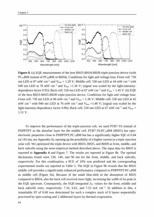
Chapter 3
84
400 500 600 700 800 900 1000 11000.0
0.1
0.2
0.3
0.4
0.5
0.6
0.7
EQ
E
Wavelength [nm]
No bias light
Front cell
Middle cell
Back cell
(a)
400 500 600 700 800 900 1000 11000.0
0.1
0.2
0.3
0.4
0.5
0.6
0.7
EQ
E
Wavelength [nm]
No bias light
Front cell
Middle cell
Back cell
(b)
Figure 9. (a) EQE measurements of the best BHJ3-BHJ4-BHJ8 triple-junction device (with
PC70BM instead of PC60BM in BHJ4). Conditions for light and voltage bias: Front cell: 730
nm LED at 87 mW cm−2 and Vbias = 1.29 V; Middle cell: 530 nm LED at 44 mW cm−2 with
940 nm LED at 78 mW cm−2 and Vbias =1.36 V; (signal was scaled by the light-intensity-
dependence factor 0.95); Back cell: 530 nm LED at 67 mW cm−2 and Vbias = 1.45 V. (b) EQE
of the best BHJ3-BHJ5-BHJ8 triple-junction device. Conditions for light and voltage bias:
Front cell: 730 nm LED at 86 mW cm−2 and Vbias = 1.36 V; Middle cell: 530 nm LED at 42
mW cm−2 with 940 nm LED at 76 mW cm−2 and Vbias =1.40 V; (signal was scaled by the
light-intensity-dependence factor 0.96); Back cell: 530 nm LED at 67 mW cm−2 and Vbias =
1.51 V.
To improve the performance of the triple-junction cell, we used PTB7-Th instead of
PDPPTPT as the absorber layer for the middle cell. PTB7-Th:PC70BM (BHJ5) has opto-
electronic properties close to PDPPTPT:PC70BM but has a significantly higher IQE of 0.84
(at 145 nm, see Appendix 4), opening up the possibility of a higher current in a triple-junction
solar cell. We optimized the triple device with BHJ3, BHJ5, and BHJ8 as front, middle, and
back subcells using the semi-empirical method described above. The input data for BHJ5 is
reported in Appendix 4 and Figure 7. The results are reported in Figure 8b. The optimal
thicknesses found were 130, 140, and 90 nm for the front, middle, and back subcells,
respectively. For this combination, a PCE of 10% was predicted and the corresponding
experimental results are reported in Table 5. The EQE in Figure 9b reveals that the BHJ5
middle cell provides a significantly enhanced performance compared to PDPPTPT:PC70BM
as middle cell (Figure 9a). Because of the small blue-shift in the absorption of BHJ5
compared to BHJ4, also the back cell received more light, increasing the width of its peak in
the EQE spectrum. Consequently, the EQE-integrated JSC values for the front, middle and
back subcells were, respectively: 7.16, 6.61, and 7.53 mA cm−2. In addition to this, a
remarkable FF of 0.68 was determined for such a complex stack of 8 layers sequentially
processed by spin-coating and 2 additional layers by thermal evaporation.

A Universal Route to Fabricate n-i-p Multi-Junction Polymer Solar Cells via Solution Processing
85
3.2.7 Synopsis
By considering the results for the tandem and triple-junction cells, we find that the
combination of D-PEDOT:PSS/nanoparticle ZnO allowed us to use the same coating
techniques to make a wide variety of layer stacks with different active layers in multi-junction
devices. Besides its versatility for processing, the D-PEDOT:PSS/nanoparticle ZnO ICL
matches the energy levels of the active layers adopted with very few exceptions where the
VOC dropped by more than 50 mV (partially due to contact issues of one of the chosen
materials, PDCBT). Regarding the FF, only a small loss was observed for some of the
tandems compared to the individual subcell devices. Using opto-electrical optimization and
by fabricating triple-junction cells, we demonstrated that the D-PEDOT:PSS/nanoparticle
ZnO combination provides an almost loss-less ICL. State-of-the-art triple-junction polymer
solar cell with 10% power conversion efficiency were fabricated in excellent yields (15/16)
where the PCE is limited by the photoactive layers.
3.3 Conclusions
We developed novel ink formulations to deposit virtually loss-less interconnecting
layers for solution-processed n-i-p multi-junction polymer solar cells, using PEDOT:PSS,
ZnO or PEIE. By selecting suitable co-solvents, we improved the film-forming properties of
the dispersions and solutions from which these materials were processed, while preserving
their optical, electrical and structural properties. The formulations are relatively simple and
can be used with a wide range of active layer materials of different chemical nature without
adjustments.
For tandem cells both ZnO and PEIE are convenient as ETL of an ICL. We reported
the results of six different tandem cells with nearly loss-less ICL performance. For fabricating
triple-junction solar cells we find that PEIE is not suitable in the bottom ICL because it
deteriorates upon deposition of the top ICL. We hypothesize that the very thin layer of PEIE
(< 10 nm) in the bottom ICL might intermix with the PEDOT:PSS at their interface as a
consequence of the processing of another layer of PEDOT:PSS on top of the middle cell.
This problem is avoided by using ZnO nanoparticles. By a more judicious choice of the active
layer materials and opto-electrical optimization, the efficiency of the triple-junction cells was
improved to 10%, with very good reproducibility, demonstrating that the ICL allows to
achieve state-of-the-art performance.
The new formulations of PEDOT:PSS, diluted in a near azeotropic water/n-propanol
mixture, and ZnO nanoparticles, dispersed in isoamyl alcohol, represent a versatile
combination to fabricate a nearly loss-less ICL for solution-processed multi-junction n-i-p
polymer solar cells. It alleviates the tedious task of developing and adjusting the ICL for each

Chapter 3
86
specific case. We encourage researchers to adopt these layers for optimizing future multi-
junction devices with novel and improved active layer materials.
3.4 Experimental Section
Materials: Pre-patterned ITO (150 nm) on glass substrates were purchased from
Naranjo Substrates. Molybdenum trioxide powder (99.97%) was purchased from Sigma
Aldrich. The ZnO was either made by a sol-gel route or from pre-formed nanoparticles with
average diameter of 4 nm, as confirmed by dynamic light scattering measurements (see the
corresponding paragraph for the synthesis). The sol-gel consisted of a solution 0.5 M
Zn(CH3COO)2·2H2O (98 %, Acros Organics) and 0.5 M ethanolamine in 2-methoxyethanol.
The suspension of D-PEDOT:PSS was prepared starting from the commercial formulation
Clevios P VPAl 4083. After filtering it with a PVDF 0.45 μm filter we diluted it with n-
propanol while vigorously stirring. For the optimal dilution ratio of 1:2 we added n-propanol
(1 mL) to VPAl 4083 (0.5 mL) in 15 minutes. The suspension was prepared fresh every time,
right before depositing PEDOT:PSS, and no further additives were used. PEIE was purchased
from Sigma Aldrich (batch 04814BGV). Starting from the pristine concentration in water,
which was 37 wt.%, we diluted in isopropanol until the total mass fraction of PEIE became
0.2 wt.% (tandems BHJ1-BHJ6, BHJ2-BHJ4 and BHJ7-BHJ7) or 0.1 wt.% (single-junction
cell of BHJ1 in Table 3 and tandem BHJ4-BHJ6). No particular stirring or additional
operation were used after the addition and the solution was stable for more than 3 weeks.
PC60BM and PC70BM were purchased from Solenne B.V. PCDTBT was purchased from 1-
Material (batch YY7276) and blended with PC70BM in a 1:4 (w/w) ratio in chlorobenzene at
a polymer concentration of 7 mg mL−1. PBDTTPD[50] was mixed with PC70BM in a 1:1.5
(w/w) ratio in chlorobenzene with 5 vol.% of 1-chloronaphthalene at a polymer concentration
of 8 mg mL−1. PDCBT[32] was blended with PC60BM in a 1:1 (w/w) ratio in chloroform
containing 1 vol.% of o-dichlorobenzene at a polymer concentration of 10 mg mL−1.
PDPP5T[33] was combined with PC60BM in 1:2 (w/w) ratio in chloroform with 10 vol.% o-
dichlorobenzene at a polymer concentration of 6 mg mL−1. PDPP3T[51] was blended with
PC60BM 1:2 (w/w) and dissolved in chloroform with 7 vol.% o-dichlorobenzene at a polymer
concentration of 5 mg mL−1. The methylated derivative PMDPP3T[4] was blended with
PC60BM 1:3 (w/w) and dissolved in chloroform containing 7 vol.% o-dichlorobenzene at a
polymer concentration of 4 mg mL−1. PDPPTPT[51] was blended with PC60BM 1:2 (w/w) or
PC70BM 1:2 (w/w) in chloroform with 6 vol.% o-dichlorobenzene at a polymer concentration
of 5 mg mL−1. PTB7-Th was purchased from 1-Material, mixed with PC70BM (1:1.5 w/w)
and dissolved in chlorobenzene containing 3 vol.% diiodooctane at a concentration of 9 mg
mL−1(reference and tandem cells) or 12 mg mL−1 (triple junction cells) of polymer.[36]
A Universal Route to Fabricate n-i-p Multi-Junction Polymer Solar Cells via Solution Processing
87
Synthesis of ZnO nanoparticles: Zinc acetate dehydrate (98%, Acros Organics) (26.53
g) was weighted in a round bottom flask and dissolved in methanol (475 mL) by stirring for
10 min. A mild argon supply was plugged to the flask as well as a reflux cooler and a dropping
funnel. The flask was set in a water bath with controllable temperature. Demineralized water
(4 mL) was added to the solution and the water bath set to 30 °C. KOH (13.26 g) was
dissolved in methanol (200 mL) and transferred to the dropping funnel. The KOH solution
was added dropwise over 15 min while vigorously stirring. After the addition the reaction
mixture appeared milky white. The temperature of the water bath was increased to 67 °C and
after 2 h, the water bath was removed and methanol (200 mL) was added to the round bottom
flask, stirring for 5 min more. At the end, the mixture looked greyish white. Stirring was
stopped and the particles were allowed to sediment for 2.5 h (a mild Ar flow was maintained).
The upper liquid was carefully removed using a pipette. Then methanol (400 mL) was added
and the suspension was stirred for 10 min. Again, stirring was stopped and the particles were
allowed to sediment for 2.5 h, under Ar flow. The clear upper liquid was removed carefully
and methanol (300 mL) was added again. Then all methanol was decanted by centrifuging
and the ZnO nanoparticles sediment was re-dispersed directly in acetone. The new dispersion
was sonicated for 3 days and filtered using a 0.2 μm PTFE filter, resulting in a clear,
translucent ZnO dispersion. The suspension was again re-dispersed in isoamyl alcohol to
achieve a ZnO concentration of 10 mg mL−1. 2-(2-Methoxyethoxy)acetic acid was added as
stabilizer to the acetone dispersion in a round bottom flask, with a concentration of 0.47 μL
mL−1. Ultra-sonication for 5 min followed and then the lower boiling point acetone was
removed by rotary evaporation at ~70 °C under vacuum.
Device fabrication: Pre-patterned ITO-coated glass substrates were cleaned by
sonication in acetone, followed by water and sodium dodecyl sulfate in water. After rinsing
in water they were again sonicated in isopropanol. To finish the cleaning, 30 min of UV-
ozone treatment preceded the spin-coating of the first layer. Sol-gel ZnO was cast directly on
clean ITO substrates by spin-coating in ambient air and annealed at 150 °C for 5 min on a
hotplate. The D-PEDOT:PSS dispersion was processed by spin-coating (45 nm for BHJ1-
BHJ6 and 60 nm for BHJ2-BHJ4 and BHJ4-BHJ6 with PEIE) or dynamic spin-coating (45
nm for BHJ1-BHJ4, BHJ7-BHJ7, BHJ3-BHJ5, BHJ5-BHJ8 tandems and the BHJ3-BHJ5-
BHJ8 triple, and 30 nm for all the other tandems and triples) in a nitrogen filled glove box
for improved wetting. The layer was kept in the vacuum at ~10−2 mbar for 30 min right after
spin-coating to remove residual solvents and no further treatment was performed. The PEIE
solution was cast by spin-coating in air to form a very thin (~10 nm) layer. The ZnO
nanoparticle dispersion was dynamically spin-coated in ambient air to give a 20 nm thick
layer, without any post treatment. The last step in the fabrication of each of these devices was
the evaporation of the top contact. In all cases this was accomplished by evaporating MoO3
(10 nm), followed by Ag (100 nm) in a vacuum chamber at ca. 6 × 10⁻⁷ mbar, through a
shadow mask. On each substrate, the intersection of the ITO pattern with the evaporated top
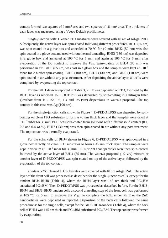
Chapter 3
88
contact formed two squares of 9 mm2 area and two squares of 16 mm2 area. The thickness of
each layer was measured using a Veeco Dektak profilometer.
Single-junction cells: Cleaned ITO substrates were covered with 40 nm of sol-gel ZnO.
Subsequently, the active layer was spin-coated following different procedures. BHJ1 (85 nm)
was spin-coated in a glove box and annealed at 70 °C for 10 min. BHJ2 (50 nm) was also
spin-coated in a glove box and used without thermal annealing. BHJ3 (130 nm) was deposited
in a glove box and annealed at 100 °C for 5 min and again at 105 °C for 5 min after
evaporation of the top contact to improve the VOC. Spin-coating of BHJ4 (85 nm) was
performed in air. BHJ5 (85 nm) was cast in a glove box and the samples were kept at ~10−2
mbar for 2 h after spin-coating. BHJ6 (100 nm), BHJ7 (130 nm) and BHJ8 (110 nm) were
spin-coated in air without any post-treatment. After depositing the active layer, all cells were
completed by evaporating the top contact.
For the BHJ1 devices reported in Table 3, PEIE was deposited on ITO, followed by the
BHJ1 layer as reported. D-PEDOT:PSS was deposited by spin-coating in a nitrogen filled
glovebox from 1:1, 1:2, 1:3, 1:4 and 1:5 (v/v) dispersions in water/n-propanol. The top
contact in this case was Ag (100 nm).
For the single-junction cells shown in Figure 4, D-PEDOT:PSS was deposited by spin-
coating on clean ITO substrates to form a 45 nm thick layer and the samples were dried at
~10−2 mbar for 30 min. PEIE was spin-coated from solutions with different solid content (0.1,
0.2 and 0.4 wt.%). BHJ7 (130 nm) was then spin-coated in air without any post treatment.
The top contact was thermally evaporated.
For the solar cells of BHJ4 shown in Figure 6, D-PEDOT:PSS was spin-coated in a
glove box directly on clean ITO substrates to form a 45 nm thick layer. The samples were
kept in vacuum at ~10−2 mbar for 30 min. PEIE or ZnO nanoparticles were then spin-coated,
followed by the active layer of BHJ4 (85 nm). The water/n-propanol (1:2 v/v) mixture or
another layer of D-PEDOT:PSS was spin-coated on top of the active layer, followed by the
evaporation of the top contact.
Tandem cells: Cleaned ITO substrates were covered with 40 nm sol-gel ZnO. The active
layer of the front cell was processed as described for the single-junctions cells, except for the
tandem BHJ4-BHJ8 (Table 4), where the BHJ4 layer was 145 nm thick and PC70BM
substituted PC60BM. Then D-PEDOT:PSS was processed as described before. For the BHJ3-
BHJ4 and BHJ3-BHJ5 tandem cells a second annealing step of the front cell was performed
at 105 °C for 5 min to improve the VOC. To complete the ICL, either PEIE or the ZnO
nanoparticles were deposited as reported. Deposition of the back cells followed the same
procedure as for the single cells, except for the BHJ3-BHJ4 tandem (Table 4), where the back
cell of BHJ4 was 145 nm thick and PC70BM substituted PC60BM. The top contact was formed
by evaporation.
A Universal Route to Fabricate n-i-p Multi-Junction Polymer Solar Cells via Solution Processing
89
The tandem BHJ1-BHJ4 differed from the others by an additional layer of D-
PEDOT:PSS (30 nm) between the BHJ4 back cell and the top contact. Also the tandem BHJ5-
BHJ8 differed from the others, using another layer of D-PEDOT:PSS between ITO and the
first layer of ZnO nanoparticles.
Triple-junction devices: For all the triple-junction cells, the fabrication started from sol-
gel ZnO (40 nm) on clean ITO substrates, followed by the first active layer as described
above. Subsequently D-PEDOT:PSS was deposited with a thickness of 30 nm (BHJ1-BHJ4-
BHJ6 and BHJ3-BHJ4-BHJ8) or 45 nm (BHJ3-BHJ5-BHJ8). Whenever the front cell was
BHJ3, a post annealing at 105 °C for 5 min was performed. After this, ZnO nanoparticles
were deposited. For the middle cell, the same thickness of BHJ4 as for the single cells was
used in the first, non-optimal triple of Table 5. In the second triple PC70BM replaced PC60BM,
and as a consequence of the optimization, a thicker active layer was used, in order to absorb
more light: 145 nm. Also for the last triple a thicker active layer of BHJ5 was adopted: 140
nm. On top of the middle cell, another layer of D-PEDOT:PSS was processed in the same
way as in the bottom ICL of each triple. Then ZnO nanoparticles followed to complete the
second ICL. After this, the top cell was spin-coated as described for single-junction cells,
with the only difference that the thickness of BHJ8 in the last triple was 90 nm. To finish, the
top contact was evaporated.
Characterization: All measurements were performed under N2 atmosphere. In order to
photodope the ZnO and MoO3 layers, 6 min of UV exposition were performed right before
the measurement for all cells. The characteristic J−V curve was measured from −2 V to +2
V for single and double-junction cells and to +2.6 V for triples. The number of voltage steps
was 401, with an integration time of 20 ms at each point. Simulated solar light from a
tungsten-halogen lamp filtered with a UV filter and daylight filter (Hoya LB120) was shined
on the cells during the measurement of the J−V characteristics. The color of the spectrum
and the intensity of it were adjusted to match the EQE-integrated JSC of the single-junction
cells, to warrant that the PCE can be determined from the J−V characteristics. To accurately
define the active area of the cells, the 4 squares from the intersection of top and bottom
contact were masked with an aperture slightly smaller than their size: 6.76 and 12.96 mm2
for the 9 and 16 mm2 squares, respectively.
The EQE was measured using a custom-made setup consisting of the following: a
tungsten-halogen lamp, a chopper, a monochromator (Oriel, Cornerstone 130), a pre-
amplifier (Stanford Research Systems SR570) and a lock-in amplifier (Stanford Research
Systems SR830 DSP). Although the setup was in ambient air, the substrates were constantly
kept sealed in a N2 filled box equipped with a quartz window. For this measurement, a
circular aperture size of 2 mm of diameter was used to define the active area. To convert the
current signal from the cell into an EQE value, a comparison was made with a reference
calibrated silicon solar cell. In the range of wavelengths 350-1050 nm, the standard deviation
Chapter 3
90
of this setup is less than 0.005 electrons/photons. As bias light, a 530, 730, and 940 nm high
power LEDs from Thorlabs were involved. The voltage bias correction was applied directly
from the pre-amplifier.
Optical modeling: This was done using the transfer matrix (TM) method using Setfos
3.2 software (Fluxim AG). By measuring transmission and reflection of each layer, we
estimated the n and k values as a function of the wavelength (see Chapter 1). To optimize the
thickness of each active layer in the triples, we used an extension of a procedure already
published for tandems.[48] This consisted in modeling iteratively the current generation of
each subcell, correcting it for the corresponding IQE. The combination of this data with the
normalized J−V characteristics of the subcells returned the J−V characteristics of the triple
for each of the tested combination of thicknesses. The determination of the voltage bias
correction for the EQE of the two optimized triples followed the procedure developed in
Chapter 4.

A Universal Route to Fabricate n-i-p Multi-Junction Polymer Solar Cells via Solution Processing
91
[1] Y. Cui, H. Yao, B. Gao, Y. Qin, S. Zhang, B. Yang, C. He, B. Xu, J. Hou, J. Am.
Chem. Soc. 2017, 139, 7302.
[2] J. Y. Kim, K. Lee, N. E. Coates, D. Moses, T.-Q. Nguyen, M. Dante, A. J. Heeger,
Science 2007, 317, 222.
[3] L. Dou, J. You, J. Yang, C.-C. Chen, Y. He, S. Murase, T. Moriarty, K. Emery, G.
Li, Y. Yang, Nat. Photonics 2012, 6, 180.
[4] W. Li, A. Furlan, K. H. Hendriks, M. M. Wienk, R. A. J. Janssen, J. Am. Chem. Soc.
2013, 135, 5529.
[5] S. Sista, M.-H. Park, Z. Hong, Y. Wu, J. Hou, W. L. Kwan, G. Li, Y. Yang, Adv.
Mater. 2010, 22, 380.
[6] J. Yang, J. You, C.-C. Chen, W.-C. Hsu, H. Tan, X. W. Zhang, Z. Hong, Y. Yang,
ACS Nano 2011, 5, 6210.
[7] H. Zhou, Y. Zhang, C. K. Mai, S. D. Collins, G. C. Bazan, T. Q. Nguyen, A. J.
Heeger, Adv. Mater. 2015, 27, 1767.
[8] K. Zhang, K. Gao, R. Xia, Z. Wu, C. Sun, J. Cao, L. Qian, W. Li, S. Liu, F. Huang,
X. Peng, L. Ding, H.-L. Yip, Y. Cao, Adv. Mater. 2016, 28, 4817.
[9] Z. Zheng, S. Zhang, J. Zhang, Y. Qin, W. Li, R. Yu, Z. Wei, J. Hou, Adv. Mater.
2016, 28, 5133.
[10] Y. Gao, V. M. Le Corre, A. Gaïtis, M. Neophytou, M. A. Hamid, K. Takanabe, P.
M. Beaujuge, Adv. Mater. 2016, 28, 3366.
[11] Y. Ma, S.-C. Chen, Z. Wang, W. Ma, J. Wang, Z. Yin, C. Tang, D. Cai, Q. Zheng,
Nano Energy 2017, 33, 313.
[12] S. Esiner, H. Van Eersel, M. M. Wienk, R. A. J. Janssen, Adv. Mater. 2013, 25,
2932.
[13] T. Becker, S. Trost, A. Behrendt, I. Shutsko, A. Polywka, P. Görrn, P. Reckers, C.
Das, T. Mayer, D. Di Carlo Rasi, K. H. Hendriks, M. M. Wienk, R. A. J. Janssen,
T. Riedl, Adv. Energy Mater. 2018, 8, 1702533.
[14] A. R. b. M. Yusoff, H. P. Kim, J. Jang, Energy Technol. 2013, 1, 212.
[15] X. Du, O. Lytken, M. S. Killian, J. Cao, T. Stubhan, M. Turbiez, P. Schmuki, H.-P.
Steinrück, L. Ding, R. H. Fink, N. Li, C. J. Brabec, Adv. Energy Mater. 2017, 7,
1601959.
[16] X. Guo, F. Liu, W. Yue, Z. Xie, Y. Geng, L. Wang, Org. Electron. 2009, 10, 1174.
[17] S. Sista, Z. Hong, M.-H. Park, Z. Xu, Y. Yang, Adv. Mater. 2010, 22, E77.
[18] C.-C. Chen, W.-H. Chang, K. Yoshimura, K. Ohya, J. You, J. Gao, Z. Hong, Y.
Yang, Adv. Mater. 2014, 26, 5670.
[19] V. C. Tung, J. Kim, L. J. Cote, J. Huang, J. Am. Chem. Soc. 2011, 133, 9262.
[20] J. Gilot, M. M. Wienk, R. A. J. Janssen, Appl. Phys. Lett. 2007, 90, 143512.
3.5 References

Chapter 3
92
[21] A. R. B. M. Yusoff, S. J. Lee, J. Kim, F. K. Shneider, W. J. da Silva, J. Jang, ACS
Appl. Mater. Interfaces 2014, 6, 13079.
[22] S. K. Hau, H.-L. Yip, K.-S. Chen, J. Zou, A. K.-Y. Jen, Appl. Phys. Lett., 2010, 97,
253307.
[23] Z. Zheng, S. Zhang, M. Zhang, K. Zhao, L. Ye, Y. Chen, B. Yang, J. Hou, Adv.
Mater. 2015, 27, 1189.
[24] Y. Zhou, C. Fuentes-Hernandez, J. W. Shim, T. M. Khan, B. Kippelen, Energy
Environ. Sci. 2012, 5, 9827
[25] J. Lee, H. Kang, J. Kong, K. Lee, Adv. Energy Mater. 2014, 4, 1301226.
[26] J. Yang, R. Zhu, Z. Hong, Y. He, A. Kumar, Y. Li, Y. Yang, Adv. Mater. 2011, 23,
3465.
[27] J. C. Gustafsson, B. Liedberg, O. Inganäs, Solid State lonics 1994, 69, 145.
[28] S. Esiner, G. W. P. van Pruissen, M. M. Wienk, R. A. J. Janssen, J. Mater. Chem.
A, 2016, 4, 5107.
[29] C. Tao, S. Ruan, X. Zhang, G. Xie, L. Shen, X. Kong, W. Dong, C. Liu, W. Chen,
Appl. Phys. Lett. 2008, 93, 193307.
[30] N. Blouin, A. Michaud, M. Leclerc, Adv. Mater. 2007, 19, 2295.
[31] C. Dyer-Smith, I. A. Howard, C. Cabanetos, A. El Labban, P. M. Beaujuge, F.
Laquai, Adv. Energy Mater. 2015, 5, 1401778.
[32] M. Zhang, X. Guo, W. Ma, H. Ade, J. Hou, Adv. Mater. 2014, 26, 5880.
[33] M. Dueggeli, M. Zaher Eteish, P. Hayoz, O. F. Aebischer, M. Fonrodona Turon, M.
G. R. Turbiez, PCT Int Appl. 2010, WO 2010049323
[34] J. C. Bijleveld, A. P. Zoombelt, S. G. J. Mathijssen, M. M. Wienk, M. Turbiez, D.
M. de Leeuw, R. A. J. Janssen, J. Am. Chem. Soc. 2009, 131, 16616.
[35] J. C. Bijleveld, V. S. Gevaerts, D. Di Nuzzo, M. Turbiez, S. G. J. Mathijssen, D. M.
de Leeuw, M. M. Wienk, R. A. J. Janssen, Adv. Mater. 2010, 22, E242.
[36] S. H. Liao, H. J. Jhuo, Y. S. Cheng, S. A. Chen, Adv. Mater. 2013, 25, 4766.
[37] S. Kouijzer, S. Esiner, C. H. Frijters, M. Turbiez, M. M. Wienk, R. A. J. Janssen,
Adv. Energy Mater. 2012, 2, 945.
[38] J. Jo, J.-R. Pouliot, D. Wynands, S. D. Collins, J. Y. Kim, T. L. Nguyen, H. Y. Woo,
Y. Sun, M. Leclerc, A. J. Heeger, Adv. Mater. 2013, 25, 4783.
[39] J.-H. Kim, C. E. Song, H. U. Kim, A. C. Grimsdale, S.-J. Moon, W. S. Shin, S. K.
Choi, D.-H. Hwang, Chem. Mater. 2013, 25, 2722
[40] P.-N. Yeh, T.-H. Jen, Y.-S. Cheng, S.-A. Chen, Sol. Energy Mater. Sol. Cells 2014,
120, 728.
[41] J.-H. Kim, C. E. Song, B. S. Kim, I.-N. Kang, W. S. Shin, D.-H Hwang, Chem.
Mater. 2014, 26, 1234.
[42] C.-Y. Chang, L. Zuo, H.-L. Yip, C.-Z. Li, Y. Li, C.-S. Hsu, Y.-J. Cheng, H. Chen,
A. K.-Y. Jen, Adv. Energy Mater. 2014, 4, 1301645.

A Universal Route to Fabricate n-i-p Multi-Junction Polymer Solar Cells via Solution Processing
93
[43] D. Gupta, M. M. Wienk, R. A. J. Janssen, ACS Appl. Mater. Interfaces 2014, 6,
13937.
[44] S. Lu, H. Lin, S. Q. Zhang, J. H. Hou, W. C. H. Choy, Adv. Energy Mater. 2017,
21, 1701164.
[45] S. M. Rowan, M. I. Newton, F. W. Driewer, G. McHale, J. Phys. Chem. B 2000,
104, 8217.
[46] Y. Zhou, C. Fuentes-Hernandez, J. Shim, J. Meyer, A. J. Giordano, H. Li, P. Winget,
T. Papadopoulos, H. Cheun, J. Kim, M. Fenoll, A. Dindar, W. Haske, E. Najafabadi,
T. M. Khan, H. Sojoudi, S. Barlow, S. Graham, J.-L. Brédas, S. R. Marder, A. Kahn,
B. Kippelen, Science 2012, 336, 327.
[47] R. Timmreck, T. Meyer, J. Gilot, H. Seifert, T. Mueller, A. Furlan, M. M. Wienk,
D. Wynands, J. Hohl-Ebinger, W. Warta, R. A. J. Janssen, M. Riede, K. Leo, Nat.
Photonics 2015, 9, 478.
[48] J. Gilot, M. M. Wienk, R. A. J. Janssen, Adv. Mater. 2010, 22, 67.
[49] A. Hadipour, B. de Boer, P. W. M. Blom, Org. Electron. 2008, 9, 617.
[50] G. Pirotte, J. Kesters, P. Verstappen, S. Govaerts, J. Manca, L. Lutsen, D.
Vanderzande, W. Maes, ChemSusChem 2015, 8, 3228.
[51] K. H. Hendriks, G. H. L. Heintges, V. S. Gevaerts, M. M. Wienk, R. A. J. Janssen,
Angew. Chemie Int. Ed. 2013, 52, 8341.


Chapter 4
Accurate Characterization of Triple-Junction
Polymer Solar Cells*
Abstract
Triple-junction device architectures represent a promising strategy to highly efficient
organic solar cells. Accurate characterization of such devices is challenging, especially with
respect to determining the external quantum efficiency (EQE) of the individual subcells. The
specific light bias conditions that are commonly used to determine the EQE of a subcell of
interest cause an excess of charge generation in the two other subcells. This results in the
build-up of an electric field over the subcell of interest, which enhances current generation
and leads to an overestimation of the EQE. A new protocol, involving optical modeling, is
developed to correctly measure the EQE of triple-junction organic solar cells. Apart from
correcting for the build-up electric field, the effect of light intensity is considered with the
help of representative single-junction cells. The short-circuit current density (JSC) determined
from integration of the EQE with the AM1.5G solar spectrum differs by up to 10% between
corrected and un-corrected protocols. The results are validated by comparing the EQE
experimentally measured to the EQE calculated via optical-electronic modeling, obtaining
an excellent agreement.
* This chapter has been published as: D. Di Carlo Rasi, K. H. Hendriks, M. M. Wienk, R.
A. J. Janssen, Adv. Energy Mater. 2017, 7, 1701664.

Chapter 4
96
4.1 Introduction
Referring to Chapter 2, it strikes that most of the studies have focused on the tandem
architecture, in which identical or different absorber layers are used, resulting in maximum
efficiencies up to 17.3%.[1] At least conceptually, stacking three absorber layers in a triple-
junction solar cell can lead to a further increase in efficiency. There are few examples of
triple-junction organic solar cells.[2-20] The gain in efficiency achieved by these triple-junction
devices was not always accompanied by a critical analysis of the measured performance. In
Chapter 2 a recent publication by Timmreck et al. was mentioned, which methodically
analyzed the literature on tandem organic solar cells, shedding light on the fact that the vast
majority of the publications on organic tandem cells lacked a proper characterization.[21] The
follow-up analysis given in Chapter 2 showed that there are still some criticalities in recent
articles on multi junctions. Although the paper focused attention on the tandem structure, the
argumentations provided can reasonably be extended to the case of triple junctions. At
present, the characterization of organic triple junctions is often limited to measuring the J−V
characteristics under simulated solar radiation and determining the EQE using different light
sources to optically bias the subcells.[2-20] Nevertheless, organic materials commonly
employed for solar cells feature peculiar characteristics that necessitate special attention for
their EQE measurement.[21-23] An accurate analysis of the effect of bias light and bias voltage
on the EQE of triple-junction organic solar cells is necessary.
Detailed protocols for the characterization of triple-junction solar cells are available in
the literature.[24] For many inorganic triple-junction solar cells the effect of bias voltage on
the spectral response is very small, which makes correction for bias voltage not critical.[24]
The aim of this work is to provide a characterization protocol for organic triple-junction solar
cells that takes into account the uniqueness of these particular materials. In order to do so,
we combine optical and electrical modeling, use representative single-junction cells, and
perform EQE measurements with appropriate light and voltage bias. We used a representative
highly efficient (~10%) triple-junction organic solar cell to develop the procedure. We found
a significant overestimation, by up to 10%, of the current generated by the subcells and the
overall efficiency, when the EQE was measured with bias light but without the correct bias
voltage. The opto-electrical modeling of the expected EQE provided a remarkably good
agreement with the experimental results, when measured correctly.

Accurate Characterization of Triple-Junction Polymer Solar Cells
97
4.2 Results and Discussion
4.2.1 The design of the triple-junction cell
Three photoactive polymers with different optical band gaps were selected for the
triple-junction device. Poly[5,5′-bis(2-butyloctyl)-(2,2′-bithiophene)-4,4′-dicarboxylate-alt-
5,5′-2,2′-bithiophene] (PDCBT) is a wide band-gap polymer (1.90 eV) that was first
presented by Zhang et al. as a polythiophene derivative with photovoltaic properties superior
to those of poly[3-hexylthiophene] (P3HT).[25] This material was blended with [6,6]-phenyl-
C61-butyric acid methyl ester (PC60BM) as acceptor to form the active layer of the front
subcell. For the middle subcell we used poly[4,8-bis(5-(2-ethylhexyl)thiophen-2-
yl)benzo[1,2-b:4,5-b′]dithiophene-co-3-fluorothieno[3,4-b]thiophene-2-carboxylate]
(PTB7-Th) with a medium band gap (1.58 eV). PTB7-Th performs remarkably well in single-
,[26] double-,[27] and triple-junction[11] solar cells. PTB7-Th was blended with [6,6]-phenyl-
C71-butyric acid methyl ester (PC70BM) to improve the current generation for the middle
subcell. For the back subcell we used poly[[2,5-bis(2-hexyldecyl-2,3,5,6-tetrahydro-3,6-
dioxopyrrolo[3,4-c]pyrrole-1,4-diyl]-alt-[3′,3″-dimethyl-2,2′:5′,2″-terthiophene]-5,5″-diyl]
(PMDPP3T). This polymer absorbs light up to 960 nm (1.30 eV) and was previously
successfully used in tandem and triple-junction solar cells with estimated efficiencies up to
9.6%.[6] PMDPP3T was blended with PC60BM, to minimize absorption of high-energy
photons in the back cell. The complete stack is shown in Figure 1.
The triple-junction cell was constructed in an inverted device geometry on a glass
substrate with patterned indium tin oxide (ITO) and a bottom electron-collecting contact
consisting of sol-gel ZnO (40 nm) and a top hole-collecting contact made from MoO3 (10
nm) covered with Ag (100 nm). For the recombination of holes and electrons between two
adjacent subcells we used an interconnecting layer, consisting of a stack of poly(3,4-
ethylenedioxythiophene) polystyrene sulfonate (PEDOT:PSS, 45 nm) and ZnO nanoparticles
(20 nm). The thickness of each photoactive layer was optimized by optical modeling based
on the transfer matrix (TM) method, combined with an empirical electrical modeling, as
described elsewhere.[28] The input for this optimization are the experimentally determined
wavelength-dependent refractive index (n) and extinction coefficient (k), the internal
quantum efficiency (IQE) of each photoactive layer as function of layer thickness, and the
normalized shape of the current density – voltage (J−V) characteristics of the three
photoactive layers, also as function of thickness.[28] The relevant data are collected in
Appendix 1, 3, 4, and Figure 1. In the optimization we kept the interconnecting layer
thickness constant and varied the thickness of the photoactive layers to find the optimal
thickness combination in terms of power conversion efficiency (PCE) (Figure 2): front cell
130 nm, middle cell 140 nm, and back cell 90 nm.

Chapter 4
98
Figure 1. (a) Structures of the semiconductor polymers used in the absorber layers. (b)
Device layout of the triple-junction polymer solar cell. Please refer to the text for a
description of the thickness values. (c) n and k values of PDCBT:PC60BM (purple), PTB7-
Th:PC70BM (blue) and PMDPP3T:PC60BM (green) as a function of the wavelength.
100 120 140 160 18080
100
120
140
160
180
Th
ickn
ess m
iddle
ce
ll [n
m]
Thickness front cell [nm]
Thickness back cell = 70 nm
100 120 140 160 18080
100
120
140
160
180
Thickness back cell = 90 nm
Th
ickn
ess m
iddle
ce
ll [n
m]
Thickness front cell [nm]
100 120 140 160 18080
100
120
140
160
180
Thickness back cell = 110 nm
Th
ickn
ess m
iddle
ce
ll [n
m]
Thickness front cell [nm]
5.5
6.0
6.5
7.0
7.5
8.0
8.5
9.0
9.5
10
PCE [%]
Figure 2. Predicted PCEs of the triple-junction solar cell as function of the thickness of the
front, middle and back cells based on optical-electrical modeling.
PDCBT PTB7-Th PMDPP3T
Glass
ITO
ZnO
PDCBT:PC60BM
PEDOT:PSS
ZnO
PTB7-Th:PC70BM
PEDOT:PSS
ZnO
PMDPP3T:PC60BM
MoO3/Ag
400 600 800 1000
1.0
1.2
1.4
1.6
1.8
2.0
2.2
2.4
n
Wavelength (nm)
PDCBT:PC60
BM
PTB7-Th:PC70
BM
PMDPP3T:PC60
BM
0.0
0.2
0.4
0.6
0.8
1.0
1.2
1.4
k
(a)
(b)(c)
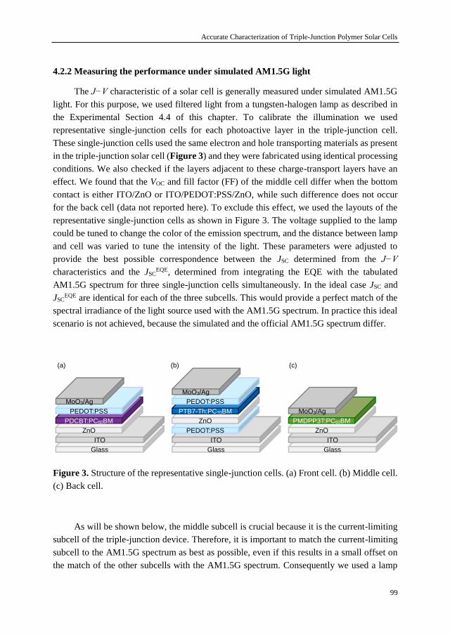
Accurate Characterization of Triple-Junction Polymer Solar Cells
99
4.2.2 Measuring the performance under simulated AM1.5G light
The J−V characteristic of a solar cell is generally measured under simulated AM1.5G
light. For this purpose, we used filtered light from a tungsten-halogen lamp as described in
the Experimental Section 4.4 of this chapter. To calibrate the illumination we used
representative single-junction cells for each photoactive layer in the triple-junction cell.
These single-junction cells used the same electron and hole transporting materials as present
in the triple-junction solar cell (Figure 3) and they were fabricated using identical processing
conditions. We also checked if the layers adjacent to these charge-transport layers have an
effect. We found that the VOC and fill factor (FF) of the middle cell differ when the bottom
contact is either ITO/ZnO or ITO/PEDOT:PSS/ZnO, while such difference does not occur
for the back cell (data not reported here). To exclude this effect, we used the layouts of the
representative single-junction cells as shown in Figure 3. The voltage supplied to the lamp
could be tuned to change the color of the emission spectrum, and the distance between lamp
and cell was varied to tune the intensity of the light. These parameters were adjusted to
provide the best possible correspondence between the JSC determined from the J−V
characteristics and the JSCEQE, determined from integrating the EQE with the tabulated
AM1.5G spectrum for three single-junction cells simultaneously. In the ideal case JSC and
JSCEQE are identical for each of the three subcells. This would provide a perfect match of the
spectral irradiance of the light source used with the AM1.5G spectrum. In practice this ideal
scenario is not achieved, because the simulated and the official AM1.5G spectrum differ.
Figure 3. Structure of the representative single-junction cells. (a) Front cell. (b) Middle cell.
(c) Back cell.
As will be shown below, the middle subcell is crucial because it is the current-limiting
subcell of the triple-junction device. Therefore, it is important to match the current-limiting
subcell to the AM1.5G spectrum as best as possible, even if this results in a small offset on
the match of the other subcells with the AM1.5G spectrum. Consequently we used a lamp
Glass
ITO
ZnO
PDCBT:PC60BM
PEDOT:PSS
MoO3/Ag
Glass
ITO
PEDOT:PSS
ZnO
PTB7-Th:PC70BM
PEDOT:PSS
MoO3/Ag
Glass
ITO
ZnO
PMDPP3T:PC60BM
MoO3/Ag
(a) (b) (c)

Chapter 4
100
setting in which the current limiting middle cell of the triple-junction provides a close
correspondence between JSC and JSCEQE, while the front and back cells are slightly
underestimated (Table 1).
Table 1. Photovoltaic parameters of representative single-junction cells and the
corresponding triple-junction cell.
Device a)
VOC
[V]
JSC
[mA cm−2]
FF
Pmax
[mW cm−2]
JSCEQE b)
[mA cm−2]
δ JSC c)
[%]
PCE d)
[%]
PDCBT 0.83 ± 0.01 8.34 ± 0.14 0.72 ± 0.02 4.96 ± 0.18 8.89 ± 0.20 −6.20 5.30 ± 0.14
PTB7-Th 0.74 ± 0.01 13.3 ± 0.1 0.52 ± 0.01 5.13 ± 0.15 13.14 ± 0.03 +1.40 5.15 ± 0.01
PMDPP3T 0.62 ± 0.01 14.8 ± 0.2 0.66 ± 0.02 5.98 ± 0.25 15.2 ± 0.3 −3.20 6.37 ± 0.01
Triple 2.15 ± 0.01 6.58 ± 0.19 0.69 ± 0.01 9.77 ± 0.29
a) The average and standard deviation are over 15 devices for the J−V measurement and over
4 devices for the EQE measurements. b) JSC determined by integrating the EQE over the
AM1.5G spectrum. c) Difference between JSC and JSC
EQE. d) Determined using JSCEQE.
4.2.3 EQE of the triple junction using bias light
The EQE of the triple-junction solar cells was first measured using only the low
intensity monochromatic probe light without any additional bias illumination. For a properly
working multi-junction solar cell, the EQE under this condition should follow the lower
envelope of the EQE of all the subcells. The presence of a low shunt resistance in one or
more subcells would result in a higher EQE.[21] The EQE of the triple measured without bias
light is shown in Figure 4 with black triangles, and nicely follows the lower envelope of the
EQE of the subcells.
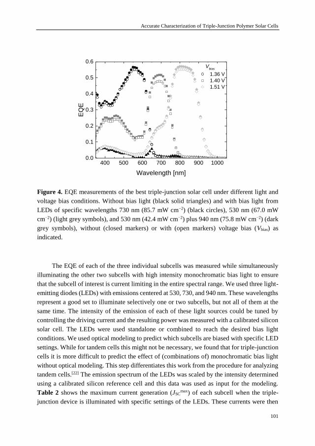
Accurate Characterization of Triple-Junction Polymer Solar Cells
101
400 500 600 700 800 900 10000.0
0.1
0.2
0.3
0.4
0.5
0.6 V
bias
1.36 V
1.40 V
1.51 VE
QE
Wavelength [nm]
Figure 4. EQE measurements of the best triple-junction solar cell under different light and
voltage bias conditions. Without bias light (black solid triangles) and with bias light from
LEDs of specific wavelengths 730 nm (85.7 mW cm−2) (black circles), 530 nm (67.0 mW
cm−2) (light grey symbols), and 530 nm (42.4 mW cm−2) plus 940 nm (75.8 mW cm−2) (dark
grey symbols), without (closed markers) or with (open markers) voltage bias (Vbias) as
indicated.
The EQE of each of the three individual subcells was measured while simultaneously
illuminating the other two subcells with high intensity monochromatic bias light to ensure
that the subcell of interest is current limiting in the entire spectral range. We used three light-
emitting diodes (LEDs) with emissions centered at 530, 730, and 940 nm. These wavelengths
represent a good set to illuminate selectively one or two subcells, but not all of them at the
same time. The intensity of the emission of each of these light sources could be tuned by
controlling the driving current and the resulting power was measured with a calibrated silicon
solar cell. The LEDs were used standalone or combined to reach the desired bias light
conditions. We used optical modeling to predict which subcells are biased with specific LED
settings. While for tandem cells this might not be necessary, we found that for triple-junction
cells it is more difficult to predict the effect of (combinations of) monochromatic bias light
without optical modeling. This step differentiates this work from the procedure for analyzing
tandem cells.[22] The emission spectrum of the LEDs was scaled by the intensity determined
using a calibrated silicon reference cell and this data was used as input for the modeling.
Table 2 shows the maximum current generation (JSCmax) of each subcell when the triple-
junction device is illuminated with specific settings of the LEDs. These currents were then
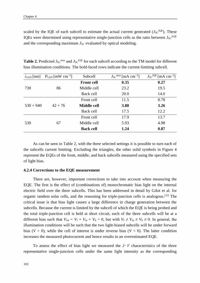
Chapter 4
102
scaled by the IQE of each subcell to estimate the actual current generated (JSCIQE). These
IQEs were determined using representative single-junction cells as the ratio between JSCEQE
and the corresponding maximum JSC evaluated by optical modeling.
Table 2. Predicted JSCmax and JSC
IQE for each subcell according to the TM model for different
bias illumination conditions. The bold-faced rows indicate the current-limiting subcell.
λLED [nm] PLED [mW cm−2] Subcell JSCmax [mA cm−2] JSC
IQE [mA cm−2]
730 86
Front cell 0.35 0.27
Middle cell 23.2 19.5
Back cell 20.0 14.0
530 + 940 42 + 76
Front cell 11.5 8.78
Middle cell 3.88 3.26
Back cell 17.5 12.2
530 67
Front cell 17.9 13.7
Middle cell 5.93 4.98
Back cell 1.24 0.87
As can be seen in Table 2, with the three selected settings it is possible to turn each of
the subcells current limiting. Excluding the triangles, the other solid symbols in Figure 4
represent the EQEs of the front, middle, and back subcells measured using the specified sets
of light bias.
4.2.4 Corrections to the EQE measurement
There are, however, important corrections to take into account when measuring the
EQE. The first is the effect of (combinations of) monochromatic bias light on the internal
electric field over the three subcells. This has been addressed in detail by Gilot et al. for
organic tandem solar cells, and the reasoning for triple-junction cells is analogous.[22] The
critical issue is that bias light causes a large difference in charge generation between the
subcells. Because the current is limited by the subcell of which the EQE is being probed and
the total triple-junction cell is held at short circuit, each of the three subcells will be at a
different bias such that Vtot = Vf + Vm + Vb = 0, but with Vf ≠ Vm ≠ Vb ≠ 0. In general, the
illumination conditions will be such that the two light-biased subcells will be under forward
bias (V > 0), while the cell of interest is under reverse bias (V < 0). The latter condition
increases the measured photocurrent and hence results in an overestimated EQE.
To assess the effect of bias light we measured the J−V characteristics of the three
representative single-junction cells under the same light intensity as the corresponding

Accurate Characterization of Triple-Junction Polymer Solar Cells
103
subcell would experience inside the light-biased triple-junction solar cell. Via optical
modeling we already established the expected short-circuit currents in each subcell under the
three different bias illumination conditions (JSCIQE in Table 2). Figure 5 shows the measured
J−V characteristics of the representative single-junction cells, where the illumination
intensity was adjusted to give JSC = JSCIQE (Table 2). Figure 5 shows how we could estimate
the reverse bias experienced by the subcell of which the EQE is measured. To perform a
correct EQE measurement, we had to apply a compensating forward bias to the triple-junction
cell. Figure 5 shows that the corrections were 1.36 V for the front subcell, 1.40 V for the
middle cell, and 1.51 V for measuring the back cell. We note that, at least in first
approximation, the bias voltage correction is close to the sum of the VOC’s of the optically
biased subcells. The resulting EQE under appropriate light and voltage bias are shown in
Figure 4 (open markers).
-2.0 -1.6 -1.2 -0.8 -0.4 0.0 0.4 0.8
-20
-15
-0.4
-0.3
-0.2
-0.1
0.0
0.1
0.2
-2.0 -1.6 -1.2 -0.8 -0.4 0.0 0.4 0.8
-14
-12
-10
-8
-6
-4
-2
0
2
-2.0 -1.6 -1.2 -0.8 -0.4 0.0 0.4 0.8
-14
-12
-10
-8
-6
-4
-2
0
2
4
Curr
en
t d
en
sity [
mA
cm
-2]
Voltage [V]
Front cell
Middle cell
Back cell
-1.36 V
(c)
(a)
Curr
en
t d
en
sity [
mA
cm
-2]
Voltage [V]
Front cell
Middle cell
Back cell
-1.40 V
(b)
Curr
en
t d
en
sity [
mA
cm
-2]
Voltage [V]
Front cell
Middle cell
Back cell
-1.51 V
Figure 5. J−V characteristics of the representative single-junction cells illuminated to give
JSC = JSCIQE as determined by optical modeling and corrected for IQE (Table 2). The current-
limiting subcell is the front cell (a), middle cell (b), and back cell (c).
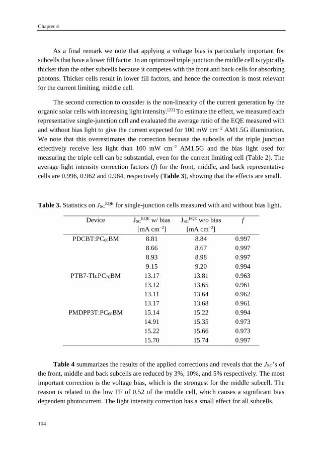
Chapter 4
104
As a final remark we note that applying a voltage bias is particularly important for
subcells that have a lower fill factor. In an optimized triple junction the middle cell is typically
thicker than the other subcells because it competes with the front and back cells for absorbing
photons. Thicker cells result in lower fill factors, and hence the correction is most relevant
for the current limiting, middle cell.
The second correction to consider is the non-linearity of the current generation by the
organic solar cells with increasing light intensity.[23] To estimate the effect, we measured each
representative single-junction cell and evaluated the average ratio of the EQE measured with
and without bias light to give the current expected for 100 mW cm−2 AM1.5G illumination.
We note that this overestimates the correction because the subcells of the triple junction
effectively receive less light than 100 mW cm−2 AM1.5G and the bias light used for
measuring the triple cell can be substantial, even for the current limiting cell (Table 2). The
average light intensity correction factors (f) for the front, middle, and back representative
cells are 0.996, 0.962 and 0.984, respectively (Table 3), showing that the effects are small.
Table 3. Statistics on JSCEQE for single-junction cells measured with and without bias light.
Device JSCEQE w/ bias
[mA cm−2]
JSCEQE w/o bias
[mA cm−2]
f
PDCBT:PC60BM 8.81 8.84 0.997
8.66 8.67 0.997
8.93 8.98 0.997
9.15 9.20 0.994
PTB7-Th:PC70BM 13.17 13.81 0.963
13.12 13.65 0.961
13.11 13.64 0.962
13.17 13.68 0.961
PMDPP3T:PC60BM 15.14 15.22 0.994
14.91 15.35 0.973
15.22 15.66 0.973
15.70 15.74 0.997
Table 4 summarizes the results of the applied corrections and reveals that the JSC’s of
the front, middle and back subcells are reduced by 3%, 10%, and 5% respectively. The most
important correction is the voltage bias, which is the strongest for the middle subcell. The
reason is related to the low FF of 0.52 of the middle cell, which causes a significant bias
dependent photocurrent. The light intensity correction has a small effect for all subcells.

Accurate Characterization of Triple-Junction Polymer Solar Cells
105
Table 4. JSCEQE (mA cm−2) of the triple-junction solar cell under representative light and
voltage bias.
Front cell Middle cell Back cell
Light bias a) 7.35 7.38 7.91
Light bias a) and voltage bias b) 7.19 6.87 7.65
Light bias a), voltage bias b), and intensity
correction c)
7.16 6.61 7.53
a) Light bias as in Table 2. b) Vf = 1.36 V, Vm = 1.40 V, Vb = 1.51 V. c) ffront = 0.996, fmiddle =
0.962, fback = 0.984.
We now reconsider the white light illumination conditions used for measuring the J−V
characteristics (Table 1). Because the middle subcell is limiting the current of the triple-
junction cell, the illumination conditions should assure that for the corresponding single-
junction cell the JSC is close to JSCEQE. At the same time the JSC’s of the front and back cells
should not be overestimated because this would increase the photocurrent. Hence, by
matching JSC to JSCEQE for the representative middle-junction cell, and having JSC < JSC
EQE for
the front and back cells (conditions chosen in Table 1) we assure an illumination close to 100
mW cm−2 AM1.5G. The resulting PCE is 9.77 ± 0.29 % when averaged over 15 devices.
4.2.5 Reconstructing the J−V-curve
Using the EQE data of the triple-junction solar cell and the J−V characteristics of the
representative single-junction solar cells it is possible to construct the expected J−V curve of
the triple solar cell. The reconstruction is performed by scaling the current under illumination
for each of the three representative single-junction solar cells, such that the JSC matches the
JSCEQE (Table 4) and then adding the voltages of the three cells for each current value. When
using the JSCEQE determined without applying the voltage bias (first line Table 4), the
reconstructed J−V curve of the triple junction (Construction 1) grossly overestimates the
experimental performance (Figure 6), but with the appropriate corrections (last line in Table
4) there is a very good correspondence (Construction 2), although small deviations can be
seen at open circuit, short circuit and in the maximum power point. (Figure 6 and Table 5).
The overestimation of the VOC by 50 mV is mainly the result of the fact that the light
intensity in each of the subcells is less than 100 mW cm−2 AM1.5G. This effect can be
estimated from ΔVOC = (kT/q)ln[JSC(triple)/JSC(single)], where JSC(triple) and JSC(single) are
the JSC of the triple and single-junction solar cells as given in Table 1. Summing the values
for the three subcells results in a combined loss of 45 mV, in fair agreement with the 50 mV
difference found experimentally.

Chapter 4
106
The deviations at short-circuit and in the maximum power point are caused by the fact
that the reconstruction does not take into account the increase of FF at lower light intensity
in each subcell. To assess the magnitude of this effect, we recorded J−V characteristics of
the representative single junction for the middle subcell, which is current limiting and has a
low FF, under the reduced light intensity that is expected in the triple-junction cell (Figure
7). At reduced light intensity the FF of the single junction increases from 0.52 to 0.58 and for
the reconstructed triple junction the FF goes from 0.63 to 0.65 (Construction 3 in Figure 6
and Table 5). The small deviation remaining compared to the experimental value of 0.68, is
attributable to the light intensity dependence of the FF in the other two cells and the
unavoidable small differences between the representative single junction configurations and
the corresponding subcells in the triple.
0.0 0.4 0.8 1.2 1.6 2.0-8
-6
-4
-2
0
Cu
rre
nt
de
nsity [
mA
cm
-2]
Voltage [V]
Experiment
Construction 1
Construction 2
Construction 3
Figure 6. Experimental J−V characteristics of the triple-junction solar cell measured under
simulated solar radiation, and reconstructed J−V curves from the measured EQE data and the
representative single-junction cells (see text for details).

Accurate Characterization of Triple-Junction Polymer Solar Cells
107
0.0 0.2 0.4 0.6 0.8
-6
-4
-2
0N
orm
aliz
ed
cu
rren
t d
en
sity
[mA
cm
-2]
Voltage [V]
PTB7-Th:PC70
BM 1 sun
PTB7-Th:PC70
BM < 1 sun
Figure 7. Normalized J−V characteristics of a PTB7-Th:PC70BM single-junction solar cell
measured under 1 sun light intensity (solid line) and under reduced light intensity, such that
the current generated was similar to the one inside the triple-junction solar cell under 1 sun
light intensity (dashed line). To provide an easier comparison of the difference in FF, the JSC
of the cell illuminated at 1 sun intensity was normalized to match the value of the cell
illuminated under reduced intensity.
Table 5. Experimental and reconstructed solar cell parameters of the best triple-junction solar
cell.
J−V characteristic VOC [V] JSC [mA cm−2] FF PCE [%]
Measured 2.15 6.86 0.68 10.03
Construction 1 2.20 7.42 0.66 10.77
Construction 2 2.20 6.98 0.63 9.71
Construction 3 2.20 6.97 0.65 9.96
Another important check is to compare the EQE of the subcells to the one predicted by
optical modeling. Figure 8 compares the experimental EQE with the absorption efficiency,
determined from the TM modeling, multiplied with the IQE determined for the corresponding
representative single-junction cells. We consider the agreement to be excellent, both in
spectral shape as well as in absolute intensity. The exceptional correspondence validates all
the steps taken in the characterization.

Chapter 4
108
400 500 600 700 800 900 1000 11000.0
0.1
0.2
0.3
0.4
0.5
0.6
Abso
rptio
n e
ffic
iency x
IQ
E, E
QE
Wavelength [nm]
Figure 8. Comparison of the experimental EQE (markers) and expected EQE (solid lines) as
determined from the product of the absorption efficiency (from TM modeling) and the IQE
(from the representative single-junction cells).
4.3 Conclusions
We developed a characterization protocol to characterize triple-junction organic solar
cells and measure the EQE of the individual subcells accurately. By using (combinations of)
three monochromatic high-power LEDs we sequentially optically biased two of the three
subcells of a polymer triple-junction solar cell to ensure that the spectral response
corresponds to the particular subcell of interest. We demonstrated that the optical bias must
be combined with an appropriate voltage bias over the triple junction in order not to
overestimate the performance. Using the modeled currents as input for the voltage bias
correction is significantly different from the approach we proposed for the tandem
characterization.[22] Without this step it is impossible to characterize the triple-junction cell
properly. The required bias voltage can be accurately determined from the J−V
characteristics of representative single-junction cells,[21,22] and lies generally within −0.1 V
from the sum of the VOC’s of the optically biased subcells. A second adjustment accounts for
the non-linearity of the photocurrent with light intensity. By combining these two corrections,
the JSCEQE integrated from the EQE and the AM1.5G solar spectrum reduced by as much as
3%, 10%, and 5% for the front, middle, and back subcells, respectively. The J−V curve
constructed using the JSCEQE from the only-light-biased measurement lead to an
overestimation of the PCE by 8% with respect to the construction in which all corrections
Accurate Characterization of Triple-Junction Polymer Solar Cells
109
were used. The reconstructed PCE = 9.96% differed by 0.07 percent point from the
experimental PCE = 10.03%. Likewise, the experimental EQE of the subcells in the triple-
junction cell and the EQE estimated from optical TM modeling and IQE of the single-
junction cells, show excellent agreement. The EQE analyses also give credence to our
adjustment procedure of the white light illumination to match the AM1.5G spectrum for this
triple-junction cell. By adjusting the light source to match the EQE-integrated JSC of each
individual absorber in the multi junction, we found optimal conditions in which the
illumination approaches the AM1.5G response. Measuring the PCE under these conditions
gave a PCE = 9.77 ± 0.29 %. The procedure provides internally consistent results and
represents a reliable method to characterize triple-junction polymer solar cells.
We note that the magnitudes of the voltage and light intensity correction will generally
depend on the nature of the photoactive layers in the subcells of the triple-junction cell and
on the intensity and spectrum of the adopted bias illumination. With respect to the solar
simulator used for recording the J−V characteristics, a close match with the AM1.5G
spectrum must be established.[21] In this work this was achieved by adjusting the spectral
radiance to match the correct AM1.5G short-circuit current density of the three representative
single-junction cells with the same illumination conditions.
We realize that characterizing triple-junction organic solar cells via this protocol
requires considerable additional effort, but stress that without proper and critical analysis a
considerable overestimation of the PCE is almost inevitable.
4.4 Experimental Section
Materials: Pre-patterned ITO (150 nm) on glass substrates were purchased from
Naranjo Substrates. Molybdenum trioxide powder (99.97%) was purchased from Sigma
Aldrich. The ZnO layers were made via a sol-gel route or by spin-coating a suspension of
pre-formed nanoparticles (see Chapter 3 for their synthesis). The former consisted of a
solution 0.5 M Zn(CH3COO)2·2H2O (98 %, Acros Organics) and 0.5 M ethanolamine in 2-
methoxyethanol.[29] The suspension of PEDOT:PSS (Clevios P, VP Al 4083) was filtered
with a 0.45 μm PVDF filter and diluted in 1-propanol 1:2 (v/v) right before use, hereafter
referred to as D-PEDOT. For the preparation of D-PEDOT, 1-propanol (1 mL) was added
dropwise to the commercial PEDOT:PSS dispersion in water (0.5 mL) over 15 minutes under
vigorous stirring. No further additives were used. Poly[5,5′-bis(2-butyloctyl)-(2,2′-
bithiophene)-4,4′-dicarboxylate-alt-5,5′-2,2′-bithiophene] (PDCBT) was synthesized
according to the procedure reported in literature and blended with PC60BM with a 1:1 weight
ratio.[25] The two components were dissolved in chloroform containing 1 vol.% of o-
dichlorobenzene at a concentration of 10 mg mL−1 of polymer. Poly[4,8-bis(5-(2-
ethylhexyl)thiophen-2-yl)benzo[1,2-b:4,5-b′]dithiophene-co-3-fluorothieno [3,4-

Chapter 4
110
b]thiophene-2-carboxylate] (PTB7-Th) was purchased from 1-Material (batch YY10228),
mixed with PC70BM (1:1.5 weight ratio) and dissolved in chlorobenzene, containing 3 vol.%
diiodooctane at a concentration of 12 mg mL−1 of polymer.[30] Poly[[2,5-bis(2-hexyldecyl-
2,3,5,6-tetrahydro-3,6-dioxopyrrolo[3,4 ‑ c]pyrrole-1,4-diyl]-alt-[3′,3″-dimethyl-2,2′:5′,2″-
terthiophene]-5,5″-diyl] (PMDPP3T) was synthesized following the reported procedure.[6]
PMDPP3T was blended with PC60BM (1:3 weight ratio) and dissolved in a solution of
chloroform, containing 7 vol.% o-dichlorobenzene. The concentration of polymer was 3 mg
mL−1.
Device fabrication: The patterned ITO substrates were cleaned by sonication in
acetone, followed by a solution of sodium dodecyl sulfate in water. They were then rinsed in
water and sonicated in isopropanol, before being treated under a UV/Ozone lamp to complete
the cleaning. In the following paragraphs the processing of all the layers made from solution
is described. Wherever mentioned, the sol-gel ZnO was cast directly on clean ITO substrates
by spin-coating in ambient air and annealed at 150 °C for 5 min on a hotplate. The D-PEDOT
solution was always processed by dynamic spin-coating (90 μL per sample) in a nitrogen
filled glove box for improved wetting to form a 45 nm thick layer. The layer was kept in the
vacuum of the antechamber for 30 min. right after spin-coating to remove residual solvents
and no further treatment was performed. The ZnO nanoparticles dispersion was dynamically
spin-coated (70 μL per sample) in ambient air to give a 20 nm thick layer, without any post
treatment. The last step in the fabrication of each of these devices was the evaporation of the
top contact. In all cases this was accomplished by evaporating MoO3 (10 nm), followed by
Ag (100 nm) in a vacuum chamber at ca. 6 × 10⁻⁷ mbar, through a shadow mask. On each
substrate, the intersection of the ITO pattern with the evaporated top contact formed two
squares of 9 mm2 area and two squares of 16 mm2 area. The thickness of each layer was
measured using a Veeco Dektak profilometer.
PDCBT:PC60BM single-junction cells: The clean ITO substrates were covered with
ZnO from the sol-gel route. Subsequently the solution of PDCBT:PC60BM was spin-coated
in a N2 filled glove box to form a layer with a thickness of 130 nm. The substrates were then
annealed in the glove box for 5 min at 100 °C. After this step, the D-PEDOT solution was
spin-coated and the samples annealed again at 105 °C for 10 min.
PTB7-Th:PC70BM single-junction cells: D-PEDOT was processed directly on clean
ITO substrates and annealed at 105 °C for 10 min in glove-box. Then the ZnO nanoparticles
were deposited as previously described, followed by the casting of the PTB7-Th:PC70BM
blend in the glove box to form a 140 nm thick layer. The substrates were then kept in vacuum
in the antechamber of the glove box for 2 hours. Subsequently, another D-PEDOT layer was
deposited.

Accurate Characterization of Triple-Junction Polymer Solar Cells
111
PMDPP3T single-junction cells: Sol-gel ZnO was processed on the clean ITO
substrate. Afterwards, the solution of PMDPP3T:PC60BM was spin-coated in ambient air to
obtain a layer of 90 nm in thickness.
Triple-junction solar cells: Sol-gel ZnO was spin-coated on clean ITO substrates. A
layer of 130 nm of PDCBT:PC60BM was processed on top in a glovebox and annealed at 100
°C for 5 min. Subsequently, the first layer of D-PEDOT was spin-coated and annealed in a
glovebox, at 105 °C for 10 min. To finish the first ICL, ZnO nanoparticles were spin-coated
on D-PEDOT, followed by 140 nm of PTB7-Th:PC70BM. After this step, the samples were
dried in vacuum for 2 hours. For the second ICL, D-PEDOT was spin-coated again. Then,
the ZnO nanoparticles layer was deposited, followed by 90 nm of PMDPP3T:PC60BM. The
cell was completed by the thermal evaporation of MoO3 (10 nm) and Ag (100 nm) at ca. 6 ×
10−7 mbar.
Characterization: Both the measurement of the J−V curve and the EQE were performed
under nitrogen atmosphere. The substrates were treated under a UV-lamp for 6 minutes
before measuring, in order to photodope the ZnO and MoO3 layers. Subsequently, the J−V
characteristics were measured with a Keithley 2400 source meter from −2 to +2V (single-
junction cells) and from −2 V to +2.6 V (triple-junction cells). 401 points per scan were
acquired, each with 20 ms integration time. The lamp used for this measurement was a
tungsten-halogen lamp which was filtered with a UV filter and a daylight filter (Hoya
LB120), calibrated to match the current integrated from the EQE spectrum of each single-
junction cell, as shown in the text. The measurements were performed through an
illumination mask with aperture sizes of 6.76 and 12.96 mm2, corresponding to the 9 mm2
and 16 mm2 nominal device areas, respectively. This defined the active area of the devices.
The EQE measurement was performed in a home-made setup, consisting of a tungsten-
halogen lamp, a chopper, a monochromator (Oriel, Cornerstone 130), a pre-amplifier
(Stanford Research Systems SR570) and a lock-in amplifier (Stanford Research Systems
SR830 DSP). The substrates were kept in a N2-filled box with a quartz window during the
duration of the measurement. The device of interest on each substrate was aligned through a
circular aperture with 2 mm of diameter, defining the active area. The signal response to the
modulated light was transformed into an EQE value by comparison with the measurement
on a calibrated silicon reference solar cell. The average standard deviation in measuring the
wavelength dependent EQE in this setup is less than 0.005 in electrons/photons for
wavelengths in the range of 350–1050 nm. The 530, 730 and 940 nm bias lights were high
power LEDs obtained from Thorlabs. The additional voltage bias was applied directly from
the pre-amplifier.
Optical modeling: Optical modeling based on the transfer matrix (TM) method was
performed using Setfos 3.2 (Fluxim). The wavelength dependent n and k values of each active

Chapter 4
112
layer were determined by transmission and reflection measurements (Chapter 1) using an
integrating sphere attachment on a Perkin-Elmer Lambda 1050 spectrophotometer. The
optimization based on IQE correction of the modeled current densities and the construction
of the J−V characteristics was performed according to a procedure previously reported and
extended for triple junction cells.[28] The same tools were used to predict the current
generation of each subcell in the triple-junction under the different light bias conditions. As
described in the main text, this was done by measuring the power density of the light sources
at a different driving current with the calibrated silicon reference cell of the EQE setup and
scaling the power profile of each LED (provided by the manufacturer) by those values. The
latter spectra were used as input for the TM calculation.

Accurate Characterization of Triple-Junction Polymer Solar Cells
113
[1] L. Meng, Y. Zhang, X. Wan, C. Li, X. Zhang, Y. Wang, X. Ke, Z. Xiao, L. Ding,
R. Xia, H.-L. Yip, Y. Cao, Y. Chen, Science 2018, DOI: 10.1126/science.aat2612.
[2] A. Yakimov, S. R. Forrest, Appl. Phys. Lett. 2002, 80, 1667
[3] J. Gilot, M. M. Wienk, R. A. J. Janssen, Appl. Phys. Lett. 2007, 90, 143512.
[4] D. W. Zhao, X. W. Sun, C. Y. Jiang, A. Kyaw, G. Q. Lo, D. L. Kwong, IEEE
Electron Device Lett. 2009, 30, 490.
[5] S. K. Hau, H.-L. Yip, K.-S. Chen, J. Zou, A. K.-Y. Jen, Appl. Phys. Lett. 2010, 97,
53307.
[6] W. Li, A. Furlan, K. H. Hendriks, M. M. Wienk, R. A. J. Janssen, J. Am. Chem. Soc.
2013, 135, 5529.
[7] S. Esiner, H. Van Eersel, M. M. Wienk, R. A. J. Janssen, Adv. Mater. 2013, 25,
2932.
[8] N. Li, D. Baran, K. Forberich, M. Turbiez, T. Ameri, F. C. Krebs, C. J. Brabec, Adv.
Energy Mater. 2013, 3, 1597.
[9] R. Meerheim, C. Körner, K. Leo, Appl. Phys. Lett. 2014, 105, 63306.
[10] X. Che, X. Xiao, J. D. Zimmerman, D. Fan, S. R. Forrest, Adv. Energy Mater. 2014,
4, 1400568.
[11] C.-C. Chen, W.-H. Chang, K. Yoshimura, K. Ohya, J. You, J. Gao, Z. Hong, Y.
Yang, Adv. Mater. 2014, 26, 5670.
[12] A. R. Bin Mohd Yusoff, D. Kim, H. P. Kim, F. K. Shneider, W. J. da Silva, J. Jang,
Energy Environ. Sci. 2015, 8, 303.
[13] F. Guo, N. Li, F. W. Fecher, N. Gasparini, C. O. R. Quiroz, C. Bronnbauer, Y. Hou,
V. V. Radmilović, V. R. Radmilović, E. Spiecker, K. Forberich, C. J. Brabec, Nat.
Commun. 2015, 6, 7730.
[14] S. Esiner, R. E. M. Willems, A. Furlan, W. Li, M. M. Wienk, R. A. J. Janssen, J.
Mater. Chem. A 2015, 3, 23936.
[15] X. Xiao, K. Lee, S. R. Forrest, Appl. Phys. Lett. 2015, 106, 213301.
[16] J. Tong, S. Xiong, Y. Zhou, L. Mao, X. Min, Z. Li, F. Jiang, W. Meng, F. Qin, T.
Liu, R. Ge, C. F.-Hernandez, B. Kippelen, Y. Zhou, Mater. Horiz. 2016, 3, 452.
[17] R. Meerheim, C. Körner, B. Oesen, K. Leo, Appl. Phys. Lett. 2016, 108, 103302.
[18] X. Zhang, L. Chen, T. Yuan, H. Huang, Z. Sui, R. Du, X. Li, Y. Lu, Q. Li, Mater.
Horizons 2016, 3, 452.
[19] X. Elias, Q. Liu, C. G.-Suriñach, R. Matheu, P. M.-Perez, A. M.-Otero, X. Sala, J.
Martorell, A. Llobet, ACS Catal. 2016, 6, 3310.
[20] H. Zhang, B. Niesen, E. Hack, S. Jenatsch, L. Wang, A. C. Véron, M. Makha, R.
Schneider, Y. Arroyo, R. Hany, F. Nüesch, Org. Electron. 2016, 30, 191.
4.5 References

Chapter 4
114
[21] R. Timmreck, T. Meyer, J. Gilot, H. Seifert, T. Mueller, A. Furlan, M. M. Wienk,
D. Wijnands, J. H.-Hebinger, W. Warta, R. A. J. Janssen, M. Riede, K. Leo, Nat.
Photonics 2015, 9, 478.
[22] J. Gilot, M. M. Wienk, R. A. J. Janssen, Adv. Funct. Mater. 2010, 20, 3904.
[23] D. J. Wehenkel, K. H. Hendriks, M. M. Wienk, R. A. J. Janssen, Org. Electron.
2012, 13, 3284.
[24] M. Meusel, C. Baur, G. Létay, A. W. Bett, W. Warta, E. Fernandez, Prog. Photovolt:
Res. Appl. 2003, 11, 499.
[25] M. Zhang, X. Guo, W. Ma, H. Ade, J. Hou, Adv. Mater. 2014, 26, 5880.
[26] S.-H. Liao, H.-J. Jhuo, P.-N. Yeh, Y.-S. Cheng, Y.-L. Li, Y.-H. Lee, S. Sharma, S.-
A. Chen, Sci. Rep. 2014, 4, 6813.
[27] H. Zhou, Y. Zhang, C. K. Mai, S. D. Collins, G. C. Bazan, T. Q. Nguyen, A. J.
Heeger, Adv. Mater. 2015, 27, 1767.
[28] J. Gilot, M. M. Wienk, R. A. J. Janssen, Adv. Mater. 2010, 22, E67.
[29] Y. Sun, J. H. Seo, C. J. Takacs, J. Seifter, A. J. Heeger, Adv. Mater. 2011, 23, 1679.
[30] S. H. Liao, H. J. Jhuo, Y. S. Cheng, S. A. Chen, Adv. Mater. 2013, 25, 4766.

Chapter 5
Quadruple-Junction Polymer Solar Cells with
Four Complementary Absorber Layers*
Abstract
A monolithic two-terminal solution-processed quadruple-junction polymer solar cell in
a n-i-p (inverted) configuration with four complementary polymer:fullerene active bulk-
heterojunction layers is presented. The subcells possess different optical band gaps ranging
from 1.90 to 1.13 eV. Optical modeling using the transfer matrix formalism enables to predict
the fraction of absorbed photons from sunlight in each subcell and determine the optimal
combination of layer thicknesses. The quadruple-junction cell, features an open-circuit
voltage of 2.45 V and has a power conversion efficiency of 7.6%, only slightly less than the
modeled value of 8.2%. The external quantum efficiency spectrum, determined with
appropriate light and voltage bias conditions, exhibits in general an excellent agreement
with modeled spectrum. The device performance is presently limited by bimolecular
recombination, which prevents using thick photoactive layers that could absorb light more
efficiently.
* This chapter has been published as: D. Di Carlo Rasi, K. H. Hendriks, M. M. Wienk, R.
A. J. Janssen, Adv. Mater. 2018, 30, 1803836.

Chapter 5
116
5.1 Introduction
The efficiency of multi-junction solar cells can be progressively increased by stacking
an increasing number of absorbers.[1] Following this approach, crystalline semiconductor
quintuple-junction solar cells and quadruple-junction thin film solar cells using amorphous
silicon have reached PCEs of 38.8% and 15.0%, respectively.[2,3]
Several solution-processed monolithic tandem and triple-junction organic solar cells
have been reported, [4,5] of which the most recent ones were discussed in Chapter 2. Solution-
processed multi-junction organic solar cells with more than three active layers have been
reported in very few occasions, in which cases the same absorber layer was repeated along
the stack.[6,7] Given the lack of complementarity in the absorption spectra of the subcells,
these multi-junction cells did not offer the opportunity to achieve a high efficiency.
Here we report a first example of a quadruple-junction polymer solar cell that features
four complementary band gap absorber layers (Figure 1a). The device comprises 14
functional layers of which 11 are processed consecutively from solution. The subcells were
fabricated using four different polymer:fullerene active layers with optical band gaps (Eg)
ranging from 1.90 to 1.13 eV and a combination of poly(3,4-ethylenedioxythiophene):
polystyrene sulfonate (PEDOT:PSS) and ZnO as interconnection layer in a n-i-p (inverted)
configuration (Figure 1a). The quadruple-junction solar cells reached a power conversion
efficiency of 7.6% with an open-circuit voltage of 2.45 V. The external quantum efficiency
(EQE) of the quadruple-junction solar cells was measured using bias light of different
wavelengths, following the protocol presented in Chapter 4 involving optical modeling and
correcting for the build-up electric field.[8]

Quadruple-Junction Polymer Solar Cells with Four Complementary Absorber Layers
117
Figure 1. (a) Device structure of the quadruple-junction solar cell and chemical structure of
the photoactive polymers featured in each subcell: (I) PDCBT:PC60BM, (II) PTB7-
Th:PC70BM, (III) PMDPP3T:PC60BM, and (IV) PDPPSDTPS:PC60BM. (b) Wavelength-
dependent n and k optical constants of the active layers used for the quadruple junction.
5.2 Results and discussion
5.2.1 Layers stack and optimization
The first cell on top of the transparent indium tin oxide (ITO)/ZnO contact consists of
poly[5,5′-bis(2-butyloctyl)-(2,2′-bithiophene)-4,4′-dicarboxylate-alt-5,5′-2,2′-bithiophene]
(PDCBT) with Eg = 1.90 eV as donor,[9] blended with [6,6]-phenyl-C61-butyric acid methyl
ester (PC60BM) as acceptor. The second photoactive layer is poly[4,8-bis(5-(2-
ethylhexyl)thiophen-2-yl)benzo[1,2-b:4,5-b′]dithiophene-co-3-fluorothieno[3,4-
b]thiophene-2-carboxylate] (PTB7-Th) having Eg = 1.58 eV in combination with [6,6]-
phenyl-C71-butyric acid methyl ester (PC70BM).[10] The third subcell comprises poly[[2,5-
bis(2-hexyldecyl-2,3,5,6-tetrahydro-3,6-dioxopyrrolo[3,4-c]pyrrole-1,4-diyl]-alt-[3′,3″-
dimethyl-2,2′:5′,2″-terthiophene]-5,5″-diyl] (PMDPP3T) with a Eg = 1.30 eV together with
PC60BM.[ 11 ] Finally the device is completed with a subcell consisting of poly[[4-(2-
ethylhexyl)-4H-dithieno[3,2-b:2',3'-d]pyrrole-2,6-diyl]-alt-2,5-selenophenediyl[2,5-bis(2-
ethylhexyl)-2,3,5,6-tetrahydro-3,6-dioxopyrrolo[3,4-c]pyrrole-1,4-diyl]-2,5-
selenophenediyl] (PDPPSDPTS), having a small band gap of Eg = 1.13 eV, combined with
PC60BM as acceptor.[12] To interconnect these cells we use layers of PEDOT:PSS, deposited
from the commercial dispersion diluted with n-propanol to near azeotropic composition
(referred to as D-PEDOT:PSS), as hole transport layer and ZnO nanoparticles, dispersed in
Glass
ITO
ZnO
PDCBT:PC60BM
D-PEDOT:PSS
ZnO
PTB7-Th:PC70BM
D-PEDOT:PSS
ZnO
PMDPP3T:PC60BM
D-PEDOT:PSS
ZnO
PDPPSDTPS:PC60BM
MoO3/Ag
(I)
(II)
(III)
(IV)
(IV)
(III)
(II)
(I)
400 600 800 1000 1200
1.0
1.2
1.4
1.6
1.8
2.0
2.2
2.4
2.6
n
Wavelength [nm]
0.0
0.2
0.4
0.6
0.8
1.0
1.2
1.4 PDCBT:PC
60BM
PTB7-Th:PC70
BM
PMDPP3T:PC60
BM
PDPPSDTPS:PC60
BM
k
(a) (b)

Chapter 5
118
isoamyl alcohol, as electron transport layer.[ 13 ] Details about the processing are in the
Experimental Section 5.4 of this chapter and were already introduced in Chapter 3.
The efficiency of the quadruple-junction solar cell strongly depends on the appropriate
matching of the current generation in each of the individual subcells. To determine the
optimal layer thicknesses for the quadruple-junction solar cell we used a combination of
experiments on representative single-junction cells (Figure 2) together with optical modeling
using the transfer matrix formalism.
Figure 2. Device scheme of representative single-junction cells of (a) PDCBT:PC60BM, (b)
PTB7-Th:PC70BM, (c) PMDPP3T:PC60BM, (d) PDPPSDTPS:PC60BM.
To this end, we determined the wavelength-dependent refractive index n(λ) and
extinction coefficient k(λ) for each photoactive layer (Figure 1b), the charge transport layers
(D-PEDOT:PSS, MoO3 and ZnO), and the electrodes (ITO, Ag). Second, the photovoltaic
performance of the four individual photoactive layers was determined as a function of the
layer thickness using single-junction cells. The details of these experiments can be found in
Appendix 1, 4-6. By using optical simulations for the single-junction cells, it is possible to
model the fraction of photons absorbed by the photoactive layers (fA(λ)) and by combining
this with the corresponding experimental EQE(λ), we determined the internal quantum
efficiency (IQE(λ)) for each layer. With these data it is possible to predict the performance
Glass
ITO
ZnO
PDCBT:PC60BM
D-PEDOT:PSS
MoO3/Ag
Glass
ITO
D-PEDOT:PSS
ZnO
PTB7-Th:PC70BM
D-PEDOT:PSS
MoO3/Ag
Glass
ITO
ZnO
PMDPP3T:PC60BM
D-PEDOT:PSS
MoO3/Ag
Glass
ITO
D-PEDOT:PSS
ZnO
PDPPSDTPS:PC60BM
MoO3/Ag
(a) (b)
(c) (d)
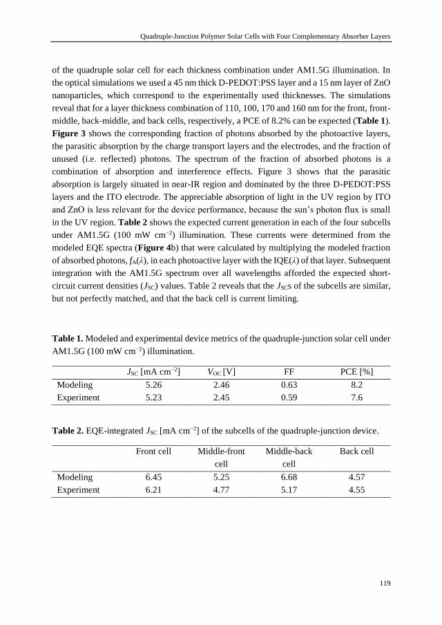
Quadruple-Junction Polymer Solar Cells with Four Complementary Absorber Layers
119
of the quadruple solar cell for each thickness combination under AM1.5G illumination. In
the optical simulations we used a 45 nm thick D-PEDOT:PSS layer and a 15 nm layer of ZnO
nanoparticles, which correspond to the experimentally used thicknesses. The simulations
reveal that for a layer thickness combination of 110, 100, 170 and 160 nm for the front, front-
middle, back-middle, and back cells, respectively, a PCE of 8.2% can be expected (Table 1).
Figure 3 shows the corresponding fraction of photons absorbed by the photoactive layers,
the parasitic absorption by the charge transport layers and the electrodes, and the fraction of
unused (i.e. reflected) photons. The spectrum of the fraction of absorbed photons is a
combination of absorption and interference effects. Figure 3 shows that the parasitic
absorption is largely situated in near-IR region and dominated by the three D-PEDOT:PSS
layers and the ITO electrode. The appreciable absorption of light in the UV region by ITO
and ZnO is less relevant for the device performance, because the sun’s photon flux is small
in the UV region. Table 2 shows the expected current generation in each of the four subcells
under AM1.5G (100 mW cm−2) illumination. These currents were determined from the
modeled EQE spectra (Figure 4b) that were calculated by multiplying the modeled fraction
of absorbed photons, fA(λ), in each photoactive layer with the IQE(λ) of that layer. Subsequent
integration with the AM1.5G spectrum over all wavelengths afforded the expected short-
circuit current densities (JSC) values. Table 2 reveals that the JSCs of the subcells are similar,
but not perfectly matched, and that the back cell is current limiting.
Table 1. Modeled and experimental device metrics of the quadruple-junction solar cell under
AM1.5G (100 mW cm−2) illumination.
JSC [mA cm−2] VOC [V] FF PCE [%]
Modeling 5.26 2.46 0.63 8.2
Experiment 5.23 2.45 0.59 7.6
Table 2. EQE-integrated JSC [mA cm−2] of the subcells of the quadruple-junction device.
Front cell Middle-front
cell
Middle-back
cell
Back cell
Modeling 6.45 5.25 6.68 4.57
Experiment 6.21 4.77 5.17 4.55

Chapter 5
120
400 600 800 1000 12000.0
0.2
0.4
0.6
0.8
1.0
Fra
ctio
n a
bsorb
ed p
ho
ton
s
Wavelength [nm]
Unused photons
Parasitic absorption
(a)
400 600 800 1000 12000.0
0.1
0.2
0.3
0.4
Fra
ctio
n a
bsorb
ed p
ho
ton
s
Wavelength [nm]
ITO
MoOx
Ag
PEDOT:PSS layers
ZnO layers
(b)
Figure 3. (a) Fraction of photons absorbed by the active layers (white background), parasitic
absorption by non-photoactive layers (black hatched area), and fraction of unused (i.e.
reflected) photons (grey hatched area) as determined by optical modeling calculations using
the transfer matrix method. (b) Individual contributions of the different non-photoactive
layers to the parasitic absorption.
0.0 0.5 1.0 1.5 2.0 2.5-6
-5
-4
-3
-2
-1
0
1
Cu
rre
nt
de
nsity [
mA
cm
-2]
Voltage [V]
Measured
Modeled
(a)
400 600 800 1000 12000.0
0.1
0.2
0.3
0.4
0.5
0.6
EQ
E
Wavelength [nm]
Vbias
1.60 V
1.65 V
1.82 V
2.13 V
(b)
Figure 4. Modeled and experimental device characteristics of the quadruple-junction solar
cell. (a) J−V characteristics under simulated AM1.5G (100 mW cm−2) illumination. (b)
Modeled (solid lines) and experimental (lines with open markers) EQEs. The experimental
EQEs were measured under representative light and voltage bias conditions.

Quadruple-Junction Polymer Solar Cells with Four Complementary Absorber Layers
121
5.2.2 Performance of the quadruple-junction solar cell
To ensure sufficient accuracy in measuring the J−V characteristic, we matched the light
source of our solar simulator in such a way that, at the thicknesses used in the quadruple-
junction device, the corresponding four single-junction cells generated virtually the same JSC
under solar simulator as the value obtained by integration of their EQE spectrum with the
AM1.5G solar spectrum. The photovoltaic performance characteristics of the representative
cells, fabricated in the same run of the quadruples, are collected in Table 3.
Table 3. Photovoltaic parameters of the reference single-junction devices. Average values
are in parentheses.
Device a)
VOC
[V]
JSC
[mA cm−2]
FF
Pmax
[mW cm−2]
JSCEQE b)
[mA cm−2]
δ JSC c)
[%]
PCE d)
[%]
PDCBT 0.83 (0.84) 7.81 (7.50) 0.72 (0.71) 4.67 (4.44) 7.58 +3.0 4.53
PTB7-Th 0.76 (0.76) 12.2 (12.0) 0.51 (0.51) 4.73 (4.64) 11.1 +9.5 4.32
PMDPP3T 0.60 (0.60) 15.2 (14.5) 0.52 (0.51) 4.74 (4.44) 15.8 -3.6 4.92
PDPPSDTPS 0.30 (0.30) 13.7 (13.0) 0.48 (0.49) 1.97 (1.90) 13.8 -0.9 1.99 a) The average is over 8 devices for the J−V measurement (7 devices for PTB7-Th) while the
EQE was measured on one device. b) JSC determined by integrating the EQE over the AM1.5G
spectrum. c) Difference between JSC and JSC
EQE. d) Determined using JSCEQE.
The measurement of the quadruple-junction devices under the calibrated light source
returned in the best case a VOC of 2.45 V, a JSC of 5.23 mA cm−2 and a FF of 0.59. Together,
these corresponded to a PCE of 7.6%, which matches the expected efficiency of 8.2% rather
well. There is an excellent match between the modeled and experimental values for JSC and
VOC and only the FF is slightly less than expected (0.59 vs. 0.63, see Table 1). Hence, the
interconnecting contact of D-PEDOT:PSS/ZnO does not lead to voltage losses. The slightly
lower FF can be due to small resistive losses in the interconnecting layers, which are not
accounted for in the modeling. Due to the intricate device fabrication, involving 11 solution-
processed layers, the yield of efficient quadruple solar cells is moderate: 6 out of 16 devices
had efficiencies above 7% with an average of 7.3 ± 0.2%. Figure 5a shows the distribution
of PCEs among all 16 devices.
To obtain more insight on the device operation, we measured the EQEs of each subcell.
Measuring the EQE of a specific subcell in a two-terminal quadruple-junction solar cell
requires that this subcell is current limiting over the entire wavelength range over which it is
measured. This can be accomplished by using appropriate bias illumination for the remaining
three subcells. Optically biased subcells, however, induce an electric field in the device which
brings the current-limiting subcell in the reverse bias regime.[14] Because the photocurrent in
Chapter 5
122
polymer solar cells depends on the applied voltage, this can result in an overestimation of the
short-circuit current density and EQE. To correct for this, a suitable bias voltage should be
applied to the quadruple-junction solar cell to compensate for this optically induced electric
field over the subcell of interest. To determine the correct bias illumination conditions we
used opto-electrical modeling,[8] and the results are collected in Table 4. This method
represents an extension of the one already developed for triple-junction cells in Chapter 4.
We approximated the bias voltage corrections as the sum of the VOCs of the representative
single-junction cells measured under AM1.5G illumination (see the Experimental Section 5.4
of this chapter). In practice this differs by only few tens of mV from the actual values.[8]
Figure 4b shows the EQE measurements of the quadruple device measured under
representative light and voltage bias conditions (open markers). Figure 5b-d shows three
additional EQE spectra for nominally identical quadruple-junction cells fabricated on
different substrates. Thanks to the judiciously selected light bias conditions, it possible to
measure the EQE of each individual subcell. Figure 5b-d demonstrates that the voltage
correction during the EQE measurement is important to not overestimate the EQEs. The
measurement without any light bias nicely follows the lower envelope of the EQEs and
suggests that leakage paths are not significant (Figure 5b-d).[15]
To give credence to these measurements, the EQE spectra in Figure 4b are compared
to the curves expected from the fraction of absorbed photons from the AM1.5G spectrum
multiplied by the wavelength-dependent IQE of each photoactive layer. With the exception
of the PMDPP3T:PC60BM middle-back cell, the agreement between experiment and
modeling is outstanding.

Quadruple-Junction Polymer Solar Cells with Four Complementary Absorber Layers
123
0 2 4 6 80
2
4
6
Co
un
ts
PCE [%]
(a)
400 600 800 1000 12000.0
0.1
0.2
0.3
0.4
0.5
0.6V
bias
1.60 V
1.65 V
1.82 V
2.13 V
no bias
EQ
E
Wavelength [nm]
(b)
400 600 800 1000 12000.0
0.1
0.2
0.3
0.4
0.5
0.6
Vbias
1.60 V
1.65 V
1.82 V
2.13 V
no bias
EQ
E
Wavelength [nm]
(c)
400 600 800 1000 12000.0
0.1
0.2
0.3
0.4
0.5
0.6
Vbias
1.60 V
1.65 V
1.82 V
2.13 V
no bias
EQ
E
Wavelength [nm]
(d)
Figure 5. (a) Distribution of the PCE values of the quadruple-junction devices measured
under simulated AM1.5G solar spectrum. Average PCE = 5.9 ± 1.5 %. (b-d) EQE spectra of
the second, third and fourth best quadruple-junction devices, each from different substrates,
acquired under representative light bias conditions, with (empty symbols) and without (filled
symbols) a voltage correction (indicated in the legend).
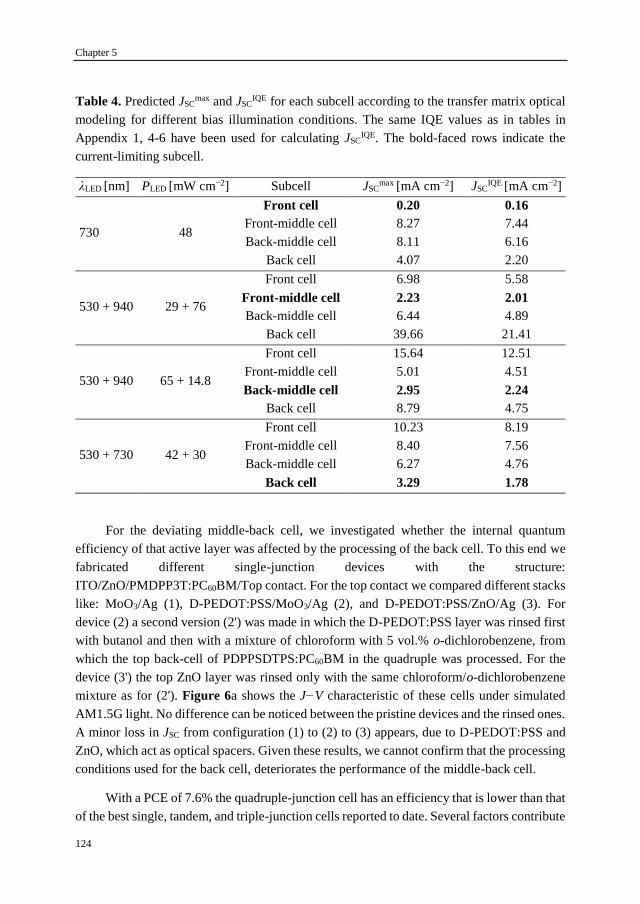
Chapter 5
124
Table 4. Predicted JSCmax and JSC
IQE for each subcell according to the transfer matrix optical
modeling for different bias illumination conditions. The same IQE values as in tables in
Appendix 1, 4-6 have been used for calculating JSCIQE. The bold-faced rows indicate the
current-limiting subcell.
λLED [nm] PLED [mW cm−2] Subcell JSCmax [mA cm−2] JSC
IQE [mA cm−2]
730 48
Front cell 0.20 0.16
Front-middle cell 8.27 7.44
Back-middle cell 8.11 6.16
Back cell 4.07 2.20
530 + 940 29 + 76
Front cell 6.98 5.58
Front-middle cell 2.23 2.01
Back-middle cell 6.44 4.89
Back cell 39.66 21.41
530 + 940 65 + 14.8
Front cell 15.64 12.51
Front-middle cell 5.01 4.51
Back-middle cell 2.95 2.24
Back cell 8.79 4.75
530 + 730 42 + 30
Front cell 10.23 8.19
Front-middle cell 8.40 7.56
Back-middle cell 6.27 4.76
Back cell 3.29 1.78
For the deviating middle-back cell, we investigated whether the internal quantum
efficiency of that active layer was affected by the processing of the back cell. To this end we
fabricated different single-junction devices with the structure:
ITO/ZnO/PMDPP3T:PC60BM/Top contact. For the top contact we compared different stacks
like: MoO3/Ag (1), D-PEDOT:PSS/MoO3/Ag (2), and D-PEDOT:PSS/ZnO/Ag (3). For
device (2) a second version (2') was made in which the D-PEDOT:PSS layer was rinsed first
with butanol and then with a mixture of chloroform with 5 vol.% o-dichlorobenzene, from
which the top back-cell of PDPPSDTPS:PC60BM in the quadruple was processed. For the
device (3') the top ZnO layer was rinsed only with the same chloroform/o-dichlorobenzene
mixture as for (2'). Figure 6a shows the J−V characteristic of these cells under simulated
AM1.5G light. No difference can be noticed between the pristine devices and the rinsed ones.
A minor loss in JSC from configuration (1) to (2) to (3) appears, due to D-PEDOT:PSS and
ZnO, which act as optical spacers. Given these results, we cannot confirm that the processing
conditions used for the back cell, deteriorates the performance of the middle-back cell.
With a PCE of 7.6% the quadruple-junction cell has an efficiency that is lower than that
of the best single, tandem, and triple-junction cells reported to date. Several factors contribute

Quadruple-Junction Polymer Solar Cells with Four Complementary Absorber Layers
125
to this. Apart from reflection losses and parasitic absorption, the EQE data in Figure 4b
clearly show that the middle-front, middle back, and back cell all use photons that should
have been absorbed by the previous layer in the stack. At the layer thicknesses used (100 –
170 nm), the photoactive materials are unable to have unit absorption. Single-junction cells
are more forgiving in this sense, because photons that are not absorbed in their first pass will
be reflected by the metal back electrode, and can be absorbed in the second pass. For multi-
junction cells, these photons are more likely to be absorbed by a subsequent layer. At present
the only way to increase the absorption efficiency of individual layers is to increase the
thickness. Unfortunately, the performance of organic bulk-heterojunction cells is affected by
bimolecular recombination, which increase with layer thickness and lowers the fill factor
(Figure 6b) and in turn, the efficiency. Hence, while multi-junction polymer solar cells offer
the perspective of reaching PCEs in excess of 20%, accomplishing such goal hinges on
developing photoactive layers which absorb more efficiently and provide less bimolecular
recombination.
0.0 0.2 0.4 0.6
-16
-12
-8
-4
0
Curr
en
t d
en
sity [
mA
cm
-2]
Voltage [V]
(1)
(2)
(2') rinsed
(3)
(3') rinsed
(a)
60 80 100 120 140 160 180 200 2200.45
0.50
0.55
0.60
0.65
0.70
0.75 PDCBT:PC
60BM
PTB7-Th:PC70
BM
PMDPP3T:PC60
BM
PDPPSDTPS:PC60
BM
FF
Thickness [nm]
(b)
Figure 6. (a) J−V characteristics of ITO/ZnO/PMDPP3T:PC60BM cells with different top
contacts: (1) MoO3/Ag; (2) D-PEDOT:PSS/MoO3/Ag; (3) D-PEDOT:PSS/ZnO/Ag as top
contact. Device (2') is similar to (2) but was rinsed first with butanol and subsequently with
a mixture of chloroform with 5 vol.% o-dichlorobenzene before depositing MoO3/Ag. Device
(3') is similar to (3) but was rinsed with a mixture of chloroform with 5 vol.% o-
dichlorobenzene before depositing MoO3/Ag. (b) FF of representative single-junction cells
as a function of the thickness of the active layer. Lines are guides to the eye.
Chapter 5
126
5.3 Conclusions
In conclusion, we combined four different photoactive polymers with complementary
absorption spectra to fabricate a first example of a quadruple-junction polymer solar cell via
solution processing. The quadruple-junction solar cell provided a PCE of 7.6 % under
simulated AM1.5G sunlight. The results were validated by a comparison with modeling,
using the J−V characteristics of representative single-junction cells and optical modeling to
determine the fraction of absorbed photons in each individual layer. The correspondence
between the measured and modeled EQE was excellent in terms of predicting the spectral
shapes and height, except for the middle-back cell were the experimental EQE was lower.
The efficiency of the quadruple-junction polymer cell is limited by bimolecular
recombination in the photoactive layers, which prevents the use of thick (>200 nm) layers to
absorb light more efficiently. Improving the efficiency of multi-junction cells, therefore
hinges on developing materials that are efficient also for thick layers. From the perspective
of the device fabrication, the present work demonstrates that it possible to process complex
device stacks (in this case 14 individual layers of which 11 are processed from solution) in a
reliable fashion with photovoltaic properties that are in very good agreement with the
expected values. This provides the framework for the development of efficient complex
multi-junction solar cells from solution.
5.4 Experimental Section
Materials: Pre-patterned ITO (170 nm) on glass substrates were purchased from
Naranjo Substrates. Molybdenum trioxide (MoO3) powder (99.97%) was purchased from
Sigma Aldrich. The ZnO layers were made via a sol-gel route or by spin-coating a suspension
of pre-formed nanoparticles in isoamyl alcohol (see Chapter 3 for their synthesis).[13] The
former consisted of a solution 0.5 M Zn(CH3COO)2·2H2O (98 %, Acros Organics) and 0.5
M ethanolamine in 2-methoxyethanol. The suspension of PEDOT:PSS (Clevios P, VP Al
4083) was diluted in 1-propanol 1:2 (v/v) right before use, referred to in the main text as D-
PEDOT:PSS (discussed in Chapter 3).[13] PDCBT,[9] PMDPP3T,[11] and PDPPSDTPS[12]
were synthesized according to procedures reported in literature. PTB7-Th was purchased
from 1-Material (batch YY10228).
Device fabrication: The patterned ITO substrates were cleaned by sonication in
acetone, followed by a solution of sodium dodecyl sulfate in water. They were then rinsed in
water and sonicated in isopropanol, before being treated under a UV/ozone lamp to complete
the cleaning. In the following paragraphs the processing of all the layers made from solution
is described. Wherever mentioned, the sol-gel ZnO was cast directly on clean ITO substrates
by spin-coating in ambient air and annealed at 150 °C for 5 min on a hotplate. The D-
Quadruple-Junction Polymer Solar Cells with Four Complementary Absorber Layers
127
PEDOT:PSS solution was always processed by dynamic spin-coating (90 μL per sample) in
a nitrogen filled glove box for improved wetting to form a 45 nm thick layer. The layer was
kept in the vacuum of the antechamber for 30 min. right after spin-coating to remove residual
solvents and no further treatment was performed. The ZnO nanoparticle dispersion was
dynamically spin-coated (70 μL per sample) in ambient air to give a 15 nm thick layer,
without any post treatment. The last step in the fabrication of each of these devices was the
evaporation of the top contact. In all cases this was accomplished by evaporating MoO3 (10
nm), followed by Ag (100 nm) in a vacuum chamber at ca. 6 × 10⁻⁷ mbar, through a shadow
mask. On each substrate, the intersection of the ITO pattern with the evaporated top contact
formed two squares of 9 mm2 area and two squares of 16 mm2 area. The thickness of each
layer was measured using a Veeco Dektak profilometer.
PDCBT:PC60BM single-junction cells: The clean ITO substrates were covered with
ZnO from the sol-gel route. The two components blended in a 1:1 weight ratio were dissolved
in chloroform containing 1 vol.% of o-dichlorobenzene at a concentration of 10 mg mL−1 of
polymer. Subsequently the solution of PDCBT:PC60BM was spin-coated in a N2 filled glove
box to form a layer with a thickness of 110 nm. The substrates were then annealed in the
glove box for 5 min at 100 °C. After this step, the D-PEDOT:PSS solution was spin-coated
and the samples annealed again at 105 °C for 10 min.
PTB7-Th:PC70BM single-junction cells: D-PEDOT:PSS was processed directly on
clean ITO substrates and annealed at 105 °C for 10 min in glove-box. Then the ZnO
nanoparticles were deposited as previously described, PTB7-Th was mixed with PC70BM
(1:1.5 weight ratio) and dissolved in chlorobenzene, containing 3 vol.% diiodooctane at a
concentration of 12 mg mL−1 of polymer and cast in the glove box to form a 100 nm thick
layer. The substrates were then kept in a vacuum of ≈10−2 mbar for 2 hours. Subsequently,
another D-PEDOT:PSS layer was deposited.
PMDPP3T:PC60BM single-junction cells: Sol-gel ZnO was processed on the clean ITO
substrate. PMDPP3T was blended with PC60BM (1:3 weight ratio) and dissolved in a solution
of chloroform, containing 7 vol.% o-dichlorobenzene. The concentration of polymer was 3
mg mL−1. The solution of PMDPP3T:PC60BM was spin-coated in ambient air to obtain a
layer of 170 nm in thickness. After this, a layer D-PEDOT:PSS was spin-coated on top.
PDPPSDTPS:PC60BM single-junction cells: D-PEDOT:PSS was processed directly on
clean ITO substrates, followed by a layer of ZnO nanoparticles. PDPPSDTPS was blended
with PC60BM (1:2 weight ratio) and together dissolved in chloroform, containing 5 vol.% o-
dichlorobenzene. The concentration of the polymer was 4 mg mL−1.The active layer was
spin-coated in the glovebox, with a thickness of 160 nm.
Quadruple-junction solar cells: Sol-gel ZnO was spin-coated on clean ITO substrates.
A layer of 110 nm of PDCBT:PC60BM was processed on top in a glovebox and annealed at

Chapter 5
128
100 °C for 5 min. Subsequently, the first layer of D-PEDOT:PSS was spin-coated and
annealed in a glovebox, at 105 °C for 10 min. To finish the first interconnecting layer (ICL),
ZnO nanoparticles were spin-coated on D-PEDOT:PSS, followed by 100 nm of PTB7-
Th:PC70BM. After this step, the samples were dried in a vacuum of ≈10−2 mbar for 2 hours.
For the second ICL, D-PEDOT:PSS was spin-coated again. Then, the ZnO nanoparticles
layer was deposited, followed by 170 nm of PMDPP3T:PC60BM. The third ICL was again
fabricated with a D-PEDOT:PSS layer, followed by the ZnO nanoparticles. The last active
layer was deposited in glovebox with a thickness of 160 nm. The cell was completed by the
thermal evaporation of MoO3 (10 nm) and Ag (100 nm) at ca. 6 × 10⁻⁷ mbar.
Characterization: Both the measurement of the J−V curve and the EQE were performed
under nitrogen atmosphere. The substrates were treated under a UV-lamp for 8 minutes
before measuring, in order to photodope the ZnO and MoO3 layers. Subsequently, the J−V
characteristics were measured with a Keithley 2400 source meter from −2 to +2V (single-
junction cells) and from −2 V to +3 V (quadruple-junction cells). 401 points per scan were
acquired, each with 20 ms integration time. The lamp used for this measurement was a
tungsten-halogen lamp which was filtered with a UV filter and a daylight filter (Hoya
LB120), calibrated to match the current integrated from the EQE spectrum of each single-
junction cell, as shown in the text. The measurements were performed through an
illumination mask with aperture sizes of 6.76 and 12.96 mm2, corresponding to the 9 mm2
and 16 mm2 nominal device areas, respectively. This defined the active area of the devices.
The EQE measurement was performed in a home-made setup, consisting of a tungsten-
halogen lamp, a chopper, a monochromator (Oriel, Cornerstone 130), a pre-amplifier
(Stanford Research Systems SR570) and a lock-in amplifier (Stanford Research Systems
SR830 DSP). The substrates were kept in a N2-filled box with a quartz window during the
duration of the measurement. The device of interest on each substrate was aligned through a
circular aperture with 2 mm of diameter, defining the active area. The signal response to the
modulated light was transformed into an EQE value by comparison with the measurement
on a calibrated silicon reference solar cell. The average standard deviation in measuring the
wavelength dependent EQE measurement in this setup is less than 0.005 in electrons/photons
for wavelengths in the range of 350–1050 nm. The 530, 730 and 940 nm bias lights were
high power LEDs obtained from Thorlabs. The additional voltage bias was applied directly
from the pre-amplifier. We measured the VOC of the representative single-junction cells under
simulated AM1.5G spectrum and we used those values to estimate the voltage bias needed
for each light bias condition. In particular, the voltage correction was the sum of the VOCs of
the optically biased subcells for each case. Since the aperture for the measurement of the
EQE was smaller (3.14 mm2) than the apertures used for the measurement of the J−V
characteristic (6.76 and 12.96 mm2), we used another mask with a 3.14 mm2 aperture to
measure again the representative single-junction cells. The measurement returned VOCs of

Quadruple-Junction Polymer Solar Cells with Four Complementary Absorber Layers
129
0.80, 0.75, 0.58 and 0.27 V for the PDCBT, PTB7-Th, PMDPP3T and the PDPPSDTPS
single cells.
Optical modeling: Optical modeling based on the transfer matrix (TM) method was
performed using Setfos 3.2 (Fluxim). The wavelength dependent n and k values of each active
layer were determined by transmission and reflection measurements using an integrating
sphere attachment on a Perkin-Elmer Lambda 1050 spectrophotometer. More details about
the procedure are provided in Chapter 1. The optimization based on IQE correction of the
modeled current densities and the construction of the J−V characteristics were performed
according to a procedure previously reported and extended for quadruple-junction cells.[16]
In order to fine tune the prediction with a more accurate estimate of the JSC generated in each
subcell, the IQE was determined as a function of the wavelength (λ). To calculate IQE(λ), we
divided the EQEs of the representative single-junction cells (Appendix 1, 4-6) by the
corresponding fractions of absorbed photons (fA(λ)) of the active layers, estimated by means
of optical modeling. Again using the optical modeling, we then calculated fA(λ) for each
active layer in the quadruple-junction cell and we multiplied these spectra by the
corresponding IQE(λ), obtaining an estimated EQE value. The calculation of the JSC value
then followed by integration with the AM1.5G reference spectrum. The same tools were used
to predict the current generation of each subcell in the quadruple-junction cell under the
different light bias conditions, similarly to the procedure developed in Chapter 4. This was
done by measuring the power density of the light sources at a different driving current with
the calibrated silicon reference cell of the EQE setup and scaling the power profile of each
LED (provided by the manufacturer) by those values. The latter spectra were used as input
for the TM calculation.
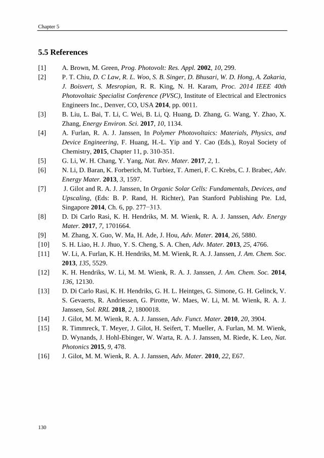
Chapter 5
130
[1] A. Brown, M. Green, Prog. Photovolt: Res. Appl. 2002, 10, 299.
[2] P. T. Chiu, D. C Law, R. L. Woo, S. B. Singer, D. Bhusari, W. D. Hong, A. Zakaria,
J. Boisvert, S. Mesropian, R. R. King, N. H. Karam, Proc. 2014 IEEE 40th
Photovoltaic Specialist Conference (PVSC), Institute of Electrical and Electronics
Engineers Inc., Denver, CO, USA 2014, pp. 0011.
[3] B. Liu, L. Bai, T. Li, C. Wei, B. Li, Q. Huang, D. Zhang, G. Wang, Y. Zhao, X.
Zhang, Energy Environ. Sci. 2017, 10, 1134.
[4] A. Furlan, R. A. J. Janssen, In Polymer Photovoltaics: Materials, Physics, and
Device Engineering, F. Huang, H.-L. Yip and Y. Cao (Eds.), Royal Society of
Chemistry, 2015, Chapter 11, p. 310-351.
[5] G. Li, W. H. Chang, Y. Yang, Nat. Rev. Mater. 2017, 2, 1.
[6] N. Li, D. Baran, K. Forberich, M. Turbiez, T. Ameri, F. C. Krebs, C. J. Brabec, Adv.
Energy Mater. 2013, 3, 1597.
[7] J. Gilot and R. A. J. Janssen, In Organic Solar Cells: Fundamentals, Devices, and
Upscaling, (Eds: B. P. Rand, H. Richter), Pan Stanford Publishing Pte. Ltd,
Singapore 2014, Ch. 6, pp. 277−313.
[8] D. Di Carlo Rasi, K. H. Hendriks, M. M. Wienk, R. A. J. Janssen, Adv. Energy
Mater. 2017, 7, 1701664.
[9] M. Zhang, X. Guo, W. Ma, H. Ade, J. Hou, Adv. Mater. 2014, 26, 5880.
[10] S. H. Liao, H. J. Jhuo, Y. S. Cheng, S. A. Chen, Adv. Mater. 2013, 25, 4766.
[11] W. Li, A. Furlan, K. H. Hendriks, M. M. Wienk, R. A. J. Janssen, J. Am. Chem. Soc.
2013, 135, 5529.
[12] K. H. Hendriks, W. Li, M. M. Wienk, R. A. J. Janssen, J. Am. Chem. Soc. 2014,
136, 12130.
[13] D. Di Carlo Rasi, K. H. Hendriks, G. H. L. Heintges, G. Simone, G. H. Gelinck, V.
S. Gevaerts, R. Andriessen, G. Pirotte, W. Maes, W. Li, M. M. Wienk, R. A. J.
Janssen, Sol. RRL 2018, 2, 1800018.
[14] J. Gilot, M. M. Wienk, R. A. J. Janssen, Adv. Funct. Mater. 2010, 20, 3904.
[15] R. Timmreck, T. Meyer, J. Gilot, H. Seifert, T. Mueller, A. Furlan, M. M. Wienk,
D. Wynands, J. Hohl-Ebinger, W. Warta, R. A. J. Janssen, M. Riede, K. Leo, Nat.
Photonics 2015, 9, 478.
[16] J. Gilot, M. M. Wienk, R. A. J. Janssen, Adv. Mater. 2010, 22, E67.
5.5 References

Chapter 6
Solution-Processed Tin Oxide-PEDOT:PSS
Interconnecting Layers for Efficient Inverted
and Conventional Tandem Polymer Solar Cells*
Abstract
Tin oxide nanoparticles are employed as electron transporting layer in solution-
processed polymer solar cells. Tin oxide based devices give excellent performance and can
interchangeably be used in conventional and inverted device configurations. In combination
with poly(3,4-ethylenedioxythiophene):polystyrene sulfonate (PEDOT:PSS) as hole
transporting layer, tin oxide forms an effective interconnecting layer (ICL) for tandem solar
cells. Conventional and inverted tandem cells with this ICL provide efficiencies up to 10.4%
in good agreement with optical-electrical modeling simulations. The critical advantage of
tin oxide in an ICL in a conventional tandem structure over the commonly used zinc oxide is
that the latter requires the use of a pH-neutral formulation of PEDOT:PSS to fabricate the
ICL, limiting the open-circuit voltage (VOC) because of its low work function. The
SnO2/PEDOT:PSS ICL, on the other hand, provides a nearly loss-free VOC.
* This chapter has been submitted for publication as: D. Di Carlo Rasi, P. M. J. G. van
Thiel, H. Bin, K. H. Hendriks, G. H. L. Heintges, M. M. Wienk, T. Becker, Y. Li, T. Riedl,
R. A. J. Janssen. Solution-Processed Tin Oxide-PEDOT:PSS Interconnecting Layers for
Efficient Inverted and Conventional Tandem Polymer Solar Cells.

Chapter 6
132
6.1 Introduction
Chapter 3 introduced a versatile processing of the ICL for inverted multi-junction
polymer solar cells.[ 1] The ICL consisted of a combination of PEDOT:PSS in a nearly
azeotropic water:1-propanol mixture as HTL and zinc oxide nanoparticles dispersed in
isoamyl alcohol as ETL. Several double-, triple- and even a quadruple-junction cells could
be realized using the same processing conditions. Unfortunately, the same materials are not
suitable to fabricate tandem devices in the conventional configuration. Due to its strong
acidity (1 < pH < 2) the PEDOT:PSS dispersion would unavoidably dissolve a previously
deposited zinc oxide layer. A workaround consists in replacing the standard acidic
formulation of PEDOT:PSS with a pH-neutral one,[2] but this is accompanied by a loss in the
work function of PEDOT:PSS from 5.05 to 4.65 eV.[3] This in turns results in a non-optimal
alignment between the Fermi level of PEDOT:PSS and the HOMO level of the electron-
donating polymer in the adjacent active layer, if this is particularly deep. As a consequence,
a loss in the open-circuit voltage (VOC) occurs.[4] First, Moet et al. proposed the use of Nafion
deposited on top of the pH-neutral PEDOT:PSS layer to recover the work function.[4] More
recently Lu et al. introduced the usage of phosphomolybdic acid as surface modifier (see
Chapter 2).[5] Although this approach was successful, it involves an additional functional
layer in the ICL, further complicating the fabrication process. Ideally, an alternative ETL
with enough chemical stability to withstand the processing of acidic PEDOT:PSS would be
required.
Solution-processed tin oxide nanoparticles have emerged as an ETL in the field of
perovskite solar cells.[ 6 ] Also sol-gel tin oxide has been used for organic photovoltaic
devices.[7,8] Recently, Becker et al. presented a tandem polymer solar cell with a molybdenum
oxide/tin oxide ICL, where these layers were deposited by thermal evaporation and atomic
layer deposition, respectively.[9] Here we demonstrate the use of commercially available tin
oxide colloidal dispersions as ETL for the solution processing of efficient single-junction and
tandem polymer solar cells with both the inverted and the conventional configuration. For
the tandems, tin oxide was used in combination with PEDOT:PSS in the ICL. Two tin oxide
formulations were considered in our study, one in water and one in a 1:1 (v/v) mixture of 1-
and 2-butanol. In single-junction cells the performance of tin oxide as ETL compares well
with a perylene diimide with amino N-oxide terminal substituents (PDINO), used as
reference ETL.[10] For the ICL in the inverted tandem configuration a SnO2 nanoparticles
formulation in butanol was used because butanol does not affect a PEDOT:PSS layer. In
conventional tandems the tin oxide layer did not dissolve during the deposition of the acidic
PEDOT:PSS dispersion. The tandem solar cells with tin oxide afforded efficiencies up to
10.4%, in good agreement with optical-electrical modeling. To further highlight the
advantage of solution-processed SnO2 layers over the ubiquitously used ZnO layers in ICLs
of conventional tandem solar cells, we demonstrate that the tandem open-circuit voltage loss

Solution-Processed Tin Oxide-PEDOT:PSS Interconnecting Layers for Efficient Inverted and Conventional
Tandem Polymer Solar Cells
133
for polymers with deep HOMO energy levels can be reduced from 200 to 20 mV when using
SnO2.
6.2 Results and Discussion
6.2.1 Single-junction Cells with SnO2 Charge Transport Layers
We fabricated single-junction cells in conventional and inverted cell configurations
using poly[(4,8-bis(5-(tripropylsilyl)thiophen-2-yl)benzo[1,2-b:4,5-b']dithiophene)-alt-(5,6-
difluoro-2-(2-hexyldecyl)-4,7-di(thiophen-2-yl)-2H-benzo[d][1,2,3]triazole)] (J71) blended
with 2,2'-[[6,6,12,12-tetrakis(4-hexylphenyl)-6,12-dihydrodithieno[2,3-d:2',3'-d']-s-
indaceno[1,2-b:5,6-b']dithiophene-2,8-diyl]bis[methylidyne(3-oxo-1H-indene-2,1(3H)-
diylidene)]]bis[propanedinitrile] (ITIC) (Figure 1).[11] For inverted devices we deposited
SnO2 nanoparticles from water (5 wt.%) on ITO as ETL (with work function (WF) of 4.0 eV)
and PEDOT:PSS as HTL from a water:1-propanol 1:2 (v/v) mixture on the bulk
heterojunction layers. For the conventional configuration we used PEDOT:PSS from water
on ITO and SnO2 nanoparticles from a mixture of 1- and 2-butanol 1:1 (v/v) on the active
layers. Further details are provided in the Experimental Section 6.4 of this chapter. Layers of
SnO2 nanoparticles have negligible optical absorption in the visible range and show an optical
band gap at 3.8-3.9 eV. As a reference, we used a device with PDINO as ETL as published
by Bin et al.[11] (Figure 1a). The photovoltaic performance of the three devices under
simulated air mass 1.5 (AM1.5G, 100 mW cm−2) solar illumination is reported in Table 1.
For 75 nm thick active layer films, the short-circuit current density is fairly close for the three
devices (14.8 < JSCEQE < 15.6 mA cm−2). Compared to the PCE of 11.4% reported by Bin et
al.[11] the reference device had unfortunately a lower performance because of a lower FF and
JSC. The FF of the conventional cell with SnO2 is slightly lower than the reference device
(0.58 vs 0.60, respectively), while it increases for the inverted cell to 0.63. The results in
Table 1 demonstrate that solution-processed SnO2 layers can be used as effective ETL in
single-junction polymer cells.
Chapter 6
134
Figure 1. Chemical structures of J71 and ITIC. (a) Reference device. (b) Conventional
device. (c) Inverted device.
Table 1. Photovoltaic parameters of J71:ITIC single-junction cells determined with
simulated AM1.5G (100 mW cm−2) illumination.
Configuration a)
VOC b)
[V]
JSC
[mA cm−2]
FF
Pmax
[mW cm−2]
JSCEQE c)
[mA cm−2]
PCE d)
[%]
Reference 0.92 (0.92) 15.1 (14.9) 0.60 (0.60) 8.34 (8.13) 15.2 8.39
Conventional 0.93 (0.93) 14.9 (14.7) 0.58 (0.58) 8.04 (7.88) 14.8 7.98
Inverted e) 0.92 (0.91) 16.1 (15.8) 0.63 (0.61) 9.33 (8.85) 15.6 9.04
a) Thickness of active layers is 75 nm. b) Values are reported for best cells with average
performance over 4 cells in parentheses. c) By integrating the EQE with the AM1.5G
spectrum. d) Calculated using JSCEQE. e) Prior to the measurement, the devices were exposed
to UV-light.
6.2.2 Tandem Solar Cells with SnO2 and PEDOT:PSS Interconnecting Layer
Prior to making tandem cells in the conventional configuration we tested the integrity
of the SnO2 layer against the subsequent deposition of an acidic aqueous PEDOT:PSS
dispersion. A SEM cross-section image shows a closed SnO2 nanoparticle layer after
depositing a PEDOT:PSS layer on top from an acidic aqueous dispersion (Figure 2). This
demonstrates that the acidic PEDOT:PSS dispersion does not deteriorate the SnO2 layer.
Glass
ITO
PEDOT:PSS
J71:ITIC
SnO2
Glass
ITO
SnO2
J71:ITIC
PEDOT:PSS
(b) (c)
Al MoO3Ag
(a)
Glass
ITO
PEDOT:PSS
J71:ITIC
PDINO
Al
J71 ITIC

Solution-Processed Tin Oxide-PEDOT:PSS Interconnecting Layers for Efficient Inverted and Conventional
Tandem Polymer Solar Cells
135
Kelvin probe experiments showed a WF of 5.0 eV for the ITO/SnO2/PEDOT:PSS stack, close
to the WF of 5.1 eV for ITO/PEDOT:PSS.
For the inverted configuration, SnO2 from butanol was spin-coated on top of
PEDOT:PSS. The WF of an ITO/PEDOT:PSS/SnO2 stack determined from Kelvin probe is
4.1 eV, compared to 4.0 eV for a ITO/SnO2 layer.
Figure 2. Colored SEM cross-section of a PEDOT:PSS layer spin-coated on a SnO2
nanoparticle layer on a Si substrate.
Next, both conventional and inverted tandem devices were fabricated, adopting
complementary active layer absorbers for the subcells. J71 blended with ITIC was used as
wide band gap front cell absorber, while poly[[2,5-bis(2-hexyldecyl-2,3,5,6-tetrahydro-3,6-
dioxopyrrolo[3,4-c]pyrrole-1,4-diyl]-alt-[3′,3″-dimethyl-2,2′:5′,2″-terthiophene]-5,5″-diyl]
(PMDPP3T) [12] in combination with [6,6]-phenyl-C61-butyric acid methyl ester (PC60BM)
was used as active layer for the small band gap back cell. Figure 3 shows a schematic of the
device stack adopted for both configurations and the chemical structures of PMDPP3T and
PC60BM.

Chapter 6
136
Figure 3. Tandem solar cells in the conventional (a) and the inverted (b) configurations.
Wavelength-dependent n and k optical constants of the active layers (c). Chemical structures
of PMDPP3T and PC60BM (d).
In order to maximize and balance the light absorption in the subcells of the tandem
devices, we performed optical simulations using the transfer matrix method on the entire
device stacks using the experimentally determined refractive index and extinction
coefficients of all layers in the stack. The wavelength-dependent refractive index (n(λ)) and
extinction coefficient (k(λ)) of the active layers are shown in Figure 3c. These optical
simulations were then combined with electrical performance data, acquired from a set of
representative single-junction devices of both the subcells, at different thickness of the active
layer to obtain the expected current density – voltage (J–V) characteristics of the tandem cells
from which the relevant expected device metrics can be determined. The details of this
method are described in the literature and in the remainder we refer to it as optical-electrical
modeling.[13] The precise device structure and photovoltaic parameters of the single-junction
cells are reported in the Experimental Section 6.4 of this chapter and Appendix 3, 7 and 8.
Figure 4 shows the contour plots of the predicted PCE for the conventional and inverted
tandem cells obtained from the optical-electrical modeling.
Glass
ITO
PEDOT:PSS
J71:ITIC
SnO2
PEDOT:PSS
PMDPP3T:PC60BM
Glass
ITO
SnO2
J71:ITIC
PEDOT:PSS
SnO2
PMDPP3T:PC60BM
(a) (b)
LiF/Al MoO3/Ag
(c)
(d)PMDPP3T PC60BM
400 600 800 1000 1200
0.8
1.0
1.2
1.4
1.6
1.8
2.0
2.2
2.4
2.6
n
Wavelength [nm]
0.0
0.2
0.4
0.6
0.8
1.0
1.2
1.4 J71:ITIC
PMDPP3T:PC60
BM
k
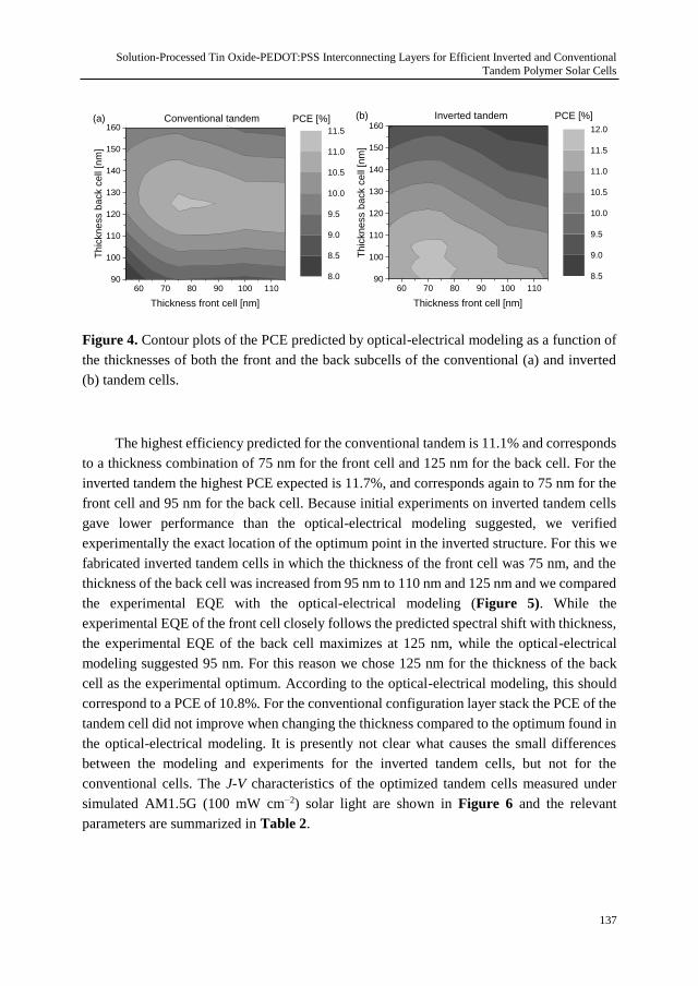
Solution-Processed Tin Oxide-PEDOT:PSS Interconnecting Layers for Efficient Inverted and Conventional
Tandem Polymer Solar Cells
137
60 70 80 90 100 11090
100
110
120
130
140
150
160(a) Conventional tandem
Th
ickn
ess b
ack c
ell
[nm
]
Thickness front cell [nm]
8.0
8.5
9.0
9.5
10.0
10.5
11.0
11.5
PCE [%]
60 70 80 90 100 11090
100
110
120
130
140
150
160
Thic
kn
ess b
ack c
ell
[nm
]
Thickness front cell [nm]
8.5
9.0
9.5
10.0
10.5
11.0
11.5
12.0
PCE [%]Inverted tandem(b)
Figure 4. Contour plots of the PCE predicted by optical-electrical modeling as a function of
the thicknesses of both the front and the back subcells of the conventional (a) and inverted
(b) tandem cells.
The highest efficiency predicted for the conventional tandem is 11.1% and corresponds
to a thickness combination of 75 nm for the front cell and 125 nm for the back cell. For the
inverted tandem the highest PCE expected is 11.7%, and corresponds again to 75 nm for the
front cell and 95 nm for the back cell. Because initial experiments on inverted tandem cells
gave lower performance than the optical-electrical modeling suggested, we verified
experimentally the exact location of the optimum point in the inverted structure. For this we
fabricated inverted tandem cells in which the thickness of the front cell was 75 nm, and the
thickness of the back cell was increased from 95 nm to 110 nm and 125 nm and we compared
the experimental EQE with the optical-electrical modeling (Figure 5). While the
experimental EQE of the front cell closely follows the predicted spectral shift with thickness,
the experimental EQE of the back cell maximizes at 125 nm, while the optical-electrical
modeling suggested 95 nm. For this reason we chose 125 nm for the thickness of the back
cell as the experimental optimum. According to the optical-electrical modeling, this should
correspond to a PCE of 10.8%. For the conventional configuration layer stack the PCE of the
tandem cell did not improve when changing the thickness compared to the optimum found in
the optical-electrical modeling. It is presently not clear what causes the small differences
between the modeling and experiments for the inverted tandem cells, but not for the
conventional cells. The J-V characteristics of the optimized tandem cells measured under
simulated AM1.5G (100 mW cm−2) solar light are shown in Figure 6 and the relevant
parameters are summarized in Table 2.
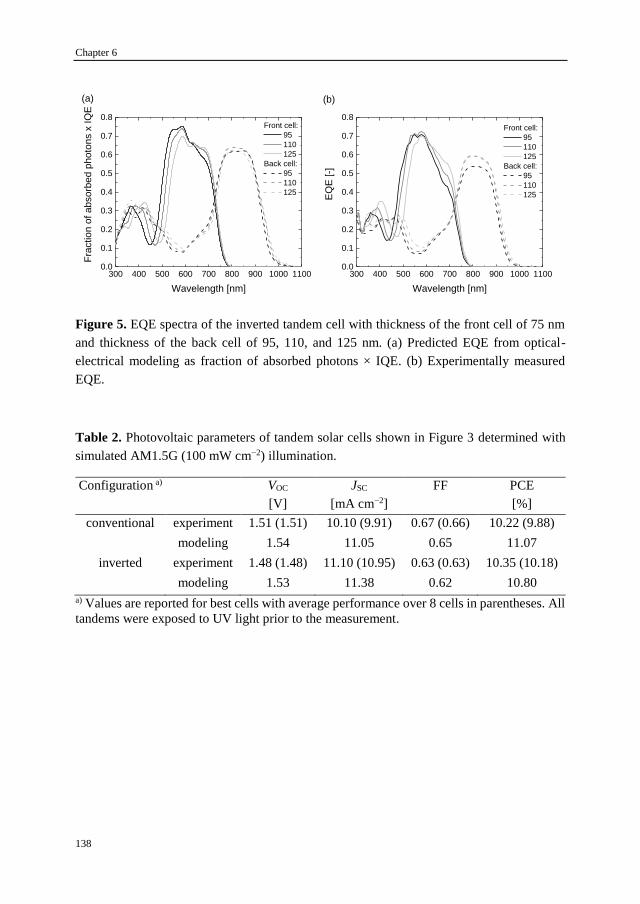
Chapter 6
138
300 400 500 600 700 800 900 1000 11000.0
0.1
0.2
0.3
0.4
0.5
0.6
0.7
0.8
Fra
ctio
n o
f a
bsorb
ed p
ho
ton
s x
IQ
E
Wavelength [nm]
Front cell:
95
110
125
Back cell:
95
110
125
(a)
300 400 500 600 700 800 900 1000 11000.0
0.1
0.2
0.3
0.4
0.5
0.6
0.7
0.8
EQ
E [-]
Wavelength [nm]
Front cell:
95
110
125
Back cell:
95
110
125
(b)
Figure 5. EQE spectra of the inverted tandem cell with thickness of the front cell of 75 nm
and thickness of the back cell of 95, 110, and 125 nm. (a) Predicted EQE from optical-
electrical modeling as fraction of absorbed photons × IQE. (b) Experimentally measured
EQE.
Table 2. Photovoltaic parameters of tandem solar cells shown in Figure 3 determined with
simulated AM1.5G (100 mW cm−2) illumination.
Configuration a)
VOC
[V]
JSC
[mA cm−2]
FF PCE
[%]
conventional experiment 1.51 (1.51) 10.10 (9.91) 0.67 (0.66) 10.22 (9.88)
modeling 1.54 11.05 0.65 11.07
inverted experiment 1.48 (1.48) 11.10 (10.95) 0.63 (0.63) 10.35 (10.18)
modeling 1.53 11.38 0.62 10.80
a) Values are reported for best cells with average performance over 8 cells in parentheses. All
tandems were exposed to UV light prior to the measurement.

Solution-Processed Tin Oxide-PEDOT:PSS Interconnecting Layers for Efficient Inverted and Conventional
Tandem Polymer Solar Cells
139
-0.2 0.0 0.2 0.4 0.6 0.8 1.0 1.2 1.4 1.6
-12
-10
-8
-6
-4
-2
0
2
Curr
en
t d
en
sity [
mA
cm
-2]
Voltage [V]
Conventional:
modeling
experiment
(a)
-0.2 0.0 0.2 0.4 0.6 0.8 1.0 1.2 1.4 1.6
-12
-10
-8
-6
-4
-2
0
2
Curr
en
t d
en
sity [
mA
cm
-2]
Voltage [V]
Inverted:
modeling
experiment
(b)
Figure 6 J-V characteristics of optimized conventional (a) and inverted (b) tandem devices
measured under simulated AM1.5G light (100 mW cm−2) (open symbols) and corresponding
predicted optical-electrical modeling (solid symbols).
With respect to the optical-electrical modeling, the VOC is only 2% lower for the
conventional structure (1.51 vs 1.54 V) and 3% lower for the inverted one (1.48 vs 1.53 V).
The fill factor (FF) is in general slightly higher than the modeling: 0.67 vs 0.65 for the
conventional cell and 0.63 vs 0.62 for the inverted tandem cell. The experimental and
modeled JSC of the conventional cell deviate by 1 mA cm−2 (10.10 vs 11.05 mA cm−2). For
the inverted tandem the experimental JSC matches rather well with the optical-electrical
modeling (11.10 vs 11.38 mA cm−2). To understand the origin of these deviations and to get
in general a better insight, we measured the external quantum efficiency (EQE) spectra of the
tandem cells. The EQEs were measured under representative light and voltage bias
conditions. The light bias is meant to isolate the response of the individual front and the back
cells, while the voltage bias corrects for the electric field induced in the device by the light
bias.[14] Light emitting diodes (LEDs) centered at 530 and 940 nm were used for optical
biasing the front and the back subcells, respectively. The required voltage bias (Vbias) was
approximated as the VOC of the representative single-junction cells, i.e. Vbias = 0.92 V for the
front cell and Vbias = 0.61 V for the back cell (Appendix 7 and 8). Figure 7 shows the EQE
under the different bias conditions. The EQE without light bias follows the lower envelope
of the EQE of the subcells, pointing that the contribution of leakage paths is relatively low.[15]
The effect of the voltage bias is relatively small, and more significant for the back cell of the
inverted tandem. The experimental and optically modeled EQE spectra for both tandem cell
configurations are shown in Figure 8. The agreement between optical-electrical modeling
and experiment is generally good for both the front and back cells. Minor differences account

Chapter 6
140
for the 1 mA cm−2 drop in the JSC for the conventional tandem, with respect to the modeling
(Table 2).
300 400 500 600 700 800 900 1000 11000.0
0.1
0.2
0.3
0.4
0.5
0.6
0.7
Vbias
0.61 V
0.92 V
EQ
E [-]
Wavelength [nm]
(a)
300 400 500 600 700 800 900 1000 11000.0
0.1
0.2
0.3
0.4
0.5
0.6
0.7(b)V
bias
0.61 V
0.92 V
EQ
E [-]
Wavelength [nm]
Figure 7. EQE spectrum of the conventional (a) and the inverted (b) tandem, as measured
under a 530 nm LED bias (grey lines), a 940 nm LED bias (black lines), with (solid lines) or
without (dashed lines) a voltage bias, indicated in the legend. The measurement without any
bias is reported with black squares.
300 400 500 600 700 800 900 1000 11000.0
0.1
0.2
0.3
0.4
0.5
0.6
0.7
0.8
EQ
E [-]
Wavelength [nm]
Conventional
modeling
experiment
(a)
300 400 500 600 700 800 900 1000 11000.0
0.1
0.2
0.3
0.4
0.5
0.6
0.7
0.8
EQ
E [-]
Wavelength [nm]
Inverted
modeling
experiment
(b)
Figure 8. Experimental (open symbols) and modeled (solid symbols) EQE spectra of (a)
conventional and (b) inverted tandem cells. The EQEs of the front cells are represented with
squares while the back cells are reported using circles.
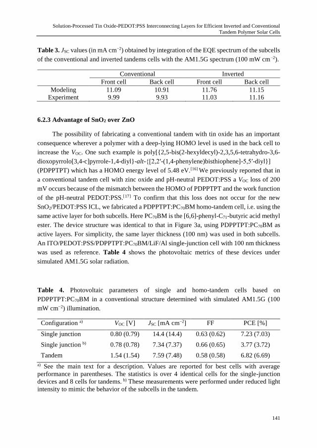
Solution-Processed Tin Oxide-PEDOT:PSS Interconnecting Layers for Efficient Inverted and Conventional
Tandem Polymer Solar Cells
141
Table 3. JSC values (in mA cm−2) obtained by integration of the EQE spectrum of the subcells
of the conventional and inverted tandems cells with the AM1.5G spectrum (100 mW cm−2).
Conventional Inverted
Front cell Back cell Front cell Back cell
Modeling 11.09 10.91 11.76 11.15
Experiment 9.99 9.93 11.03 11.16
6.2.3 Advantage of SnO2 over ZnO
The possibility of fabricating a conventional tandem with tin oxide has an important
consequence wherever a polymer with a deep-lying HOMO level is used in the back cell to
increase the VOC. One such example is poly[{2,5-bis(2-hexyldecyl)-2,3,5,6-tetrahydro-3,6-
dioxopyrrolo[3,4-c]pyrrole-1,4-diyl}-alt-{[2,2′-(1,4-phenylene)bisthiophene]-5,5′-diyl}]
(PDPPTPT) which has a HOMO energy level of 5.48 eV.[16] We previously reported that in
a conventional tandem cell with zinc oxide and pH-neutral PEDOT:PSS a VOC loss of 200
mV occurs because of the mismatch between the HOMO of PDPPTPT and the work function
of the pH-neutral PEDOT:PSS.[17] To confirm that this loss does not occur for the new
SnO2/PEDOT:PSS ICL, we fabricated a PDPPTPT:PC70BM homo-tandem cell, i.e. using the
same active layer for both subcells. Here PC70BM is the [6,6]-phenyl-C71-butyric acid methyl
ester. The device structure was identical to that in Figure 3a, using PDPPTPT:PC70BM as
active layers. For simplicity, the same layer thickness (100 nm) was used in both subcells.
An ITO/PEDOT:PSS/PDPPTPT:PC70BM/LiF/Al single-junction cell with 100 nm thickness
was used as reference. Table 4 shows the photovoltaic metrics of these devices under
simulated AM1.5G solar radiation.
Table 4. Photovoltaic parameters of single and homo-tandem cells based on
PDPPTPT:PC70BM in a conventional structure determined with simulated AM1.5G (100
mW cm−2) illumination.
Configuration a) VOC [V] JSC [mA cm−2] FF PCE [%]
Single junction 0.80 (0.79) 14.4 (14.4) 0.63 (0.62) 7.23 (7.03)
Single junction b) 0.78 (0.78) 7.34 (7.37) 0.66 (0.65) 3.77 (3.72)
Tandem 1.54 (1.54) 7.59 (7.48) 0.58 (0.58) 6.82 (6.69)
a) See the main text for a description. Values are reported for best cells with average
performance in parentheses. The statistics is over 4 identical cells for the single-junction
devices and 8 cells for tandems. b) These measurements were performed under reduced light
intensity to mimic the behavior of the subcells in the tandem.

Chapter 6
142
Having the same active layer in both subcells, the VOC of the tandem is expected to be
twice that of the single-junction cell (1.60 V). Experimentally, the tandem cells had a VOC of
1.54 V, which is 4% lower than expected. Part of this loss is due to the reduced light intensity
experienced by the subcells. This loss can be estimated from ΔVOC =
(kT/q)ln[JSC(tandem)/JSC(single)], where JSC(tandem) and JSC(single) are the JSC values of the
tandem and the single-junction cells (Table 4), and k Boltzmann constant, T the temperature,
and q the elementary charge. Since the same absorber is used in both subcells, JSC(tandem)
roughly corresponds to half the JSC(single) value, as confirmed by the results in Table 4 (7.59
vs 14.4 mA cm−2, respectively). Therefore, we can expect an 18 mV loss at each junction,
accounting in total to 36 mV. To confirm this, the reference single-junction cell was also
measured at reduced light intensity, such that it was giving a similar JSC as the tandem cell.
The VOC measured in this way was 20 mV lower, very close to the predicted loss of 18 mV.
The VOC loss of the tandem which is not directly attributable to the reduced light intensity is
then only 20 mV. This result is significantly better than what reported earlier for a similar
tandem using zinc oxide and pH-neutral PEDOT:PSS, where the VOC loss was 200 mV.[17]
This confirms that a SnO2/acidic-PEDOT:PSS ICL gives superior performance compared to
a ZnO/pH-neutral-PEDOT:PSS ICL for polymers with deep HOMO levels.
6.3 Conclusions
Commercially available tin oxide nanoparticles dispersions in water or butanol are
adopted in the fabrication of polymer solar cells. Both conventional (p-i-n) and inverted (n-
i-p) solar cells can be build using tin oxide as ETL and PEDOT:PSS as HTL in the
interconnecting layer. The two materials are not only chemically compatible with each other,
but they also provide an effective interconnection of the subcells, as demonstrated by two
high efficiency tandems with PCEs of 10.2% (conventional) and 10.4% (inverted), in good
agreement with the performance predicted by optical-electrical modeling. The use of SnO2
and its resilience against acidic aqueous PEDOT:PSS dispersions compared to the
traditionally used ZnO, has an important advantage when donor materials with deep-lying
HOMO energy level are involved. As an example, a homo-tandem cell with two
PDPPTPT:PC70BM active layers shows nearly a negligible voltage loss (20 mV) when
compared to the 200 mV loss reported for a similar device based on zinc oxide and pH-neutral
PEDOT:PSS.[17] In conclusion, SnO2 and PEDOT:PSS can be used as ICL for efficient
conventional and inverted tandem cells, without the need of additional layers to reach optimal
performance. Together, these results pave the way to new possibilities in the framework of
manufacturing efficient multi-junction organic solar cells.

Solution-Processed Tin Oxide-PEDOT:PSS Interconnecting Layers for Efficient Inverted and Conventional
Tandem Polymer Solar Cells
143
6.4 Experimental Section
Materials: Pre-patterned ITO (190 nm) on glass substrates were purchased from
Naranjo Substrates. Molybdenum trioxide powder (99.97%) was purchased from Sigma
Aldrich. The tin oxide layers were made by spin-coating a suspension of pre-formed
nanoparticles. These were either tin oxide in water (15 wt.%, Alfa Aesar) or in a mixture of
1- and 2-butanol 1:1 (v/v) (N31, 2.5 wt.%, Avantama). The concentration was adapted by
diluting the stock dispersion with water or 1-butanol, respectively. The suspension of
PEDOT:PSS (Clevios P, VP Al 4083) was filtered with a 0.45 µm PVDF filter and directly
used or diluted with 1-propanol while vigorously stirring (referred to as D-PEDOT:PSS, see
Chapter 3).[1] A dilution ratio of 1:2 (v/v) was used by adding n-propanol (1 mL) to VP Al
4083 (0.5 mL) in 15 minutes under constant vigorous stirring. The suspension was prepared
right before depositing D-PEDOT:PSS, and no further additives were used. PDINO was
synthesized according to the procedure reported in literature and dissolved in methanol with
a concentration of 1 mg mL−1.[10] PC60BM and PC70BM were purchased from Solenne while
ITIC was purchased from Solarmer. Poly[(4,8-bis(5-(tripropylsilyl)thiophen-2-yl)benzo[1,2-
b:4,5-b']dithiophene)-alt-(5,6-difluoro-2-(2-hexyldecyl)-4,7-di(thiophen-2-yl)-2H-
benzo[d][1,2,3]triazole)] (J71) was synthesized according to the procedure reported in
literature and blended with ITIC with a 1:1 weight ratio.[11] The two components were
dissolved in chloroform at a concentration of 6 mg mL−1 of polymer. Poly[[2,5-bis(2-
hexyldecyl-2,3,5,6-tetrahydro-3,6-dioxopyrrolo[3,4‑c]pyrrole-1,4-diyl]-alt-[3′,3″-dimethyl-
2,2′:5′,2″-terthiophene]-5,5″-diyl] (PMDPP3T) was synthesized following the reported
procedure.[12] PMDPP3T was blended with PC60BM (1:3 weight ratio) and dissolved in a
solution of chloroform, containing 7 vol.% o-dichlorobenzene. The concentration of polymer
was 3 mg mL−1. Poly[{2,5-bis(2-hexyldecyl)-2,3,5,6-tetrahydro-3,6-dioxopyrrolo[3,4-
c]pyrrole-1,4-diyl}-alt-{[2,2′-(1,4-phenylene)bisthiophene]-5,5′-diyl}] (PDPPTPT) was
synthesized according to the procedure reported in literature.[16] This polymer was blended
with PC70BM 1:2 (w/w) in chloroform with 6 vol.% o-dichlorobenzene at a polymer
concentration of 5 mg mL−1.
Device Fabrication: The patterned ITO substrates were cleaned by sonication in
acetone, followed by a solution of sodium dodecyl sulfate in water. They were then rinsed in
water and sonicated in isopropanol, before being treated under a UV/Ozone lamp to complete
the cleaning. Molybdenum oxide (10 nm), silver (100 nm), lithium fluoride (1 nm) and
aluminum (100 nm) were thermally evaporated in a vacuum chamber at ≈ 6 × 10⁻⁷ mbar,
through a shadow mask. On each substrate, the intersection of the ITO pattern with the
evaporated top contact formed two squares of 9 mm2 area and two squares of 16 mm2 area.
The thickness of each layer was measured using a Veeco Dektak profilometer. The
fabrication of the various device stacks described in this study is detailed in the following
paragraphs.
Chapter 6
144
J71:ITIC Single-Junction Cell (Conventional) (1): The filtered PV Al 4083 was coated
on clean ITO substrates with a thickness value of 50 nm and annealed at 140 °C for 10 min.
The J71:ITIC blend was deposited in a N2 filled glove box to form a layer with thickness of
75 nm and annealed at 150 °C for 10 min. After this, a different ETL was deposited for the
reference device and the tin oxide based device. In one case, PDINO was deposited in
glovebox, with a thickness of 3 nm. In the other case, tin oxide in butanol (2.5 wt.%) was
deposited by dynamic spin-coating in glove box and dried at ≈ 10−2 mbar for 2 hours. This
layer served as wetting layer for the subsequent deposition of tin oxide in water (2.5 wt.%)
by dynamic spin-coating in ambient air. Also this layer was dried at ≈ 10−2 mbar for 30 min.
The final thickness of the tin oxide layer was 35 nm. We encountered a suboptimal
performance of the device when using only the first layer of tin oxide in butanol, possibly
due to an unfavorable morphology of the layer. For this reason we opted for the combination
of the two formulations, here reported. At last, both the reference and the tin oxide device
were completed by evaporating the aluminum top contact.
J71:ITIC Single-Junction Cell (Inverted) (2): Clean ITO substrates were covered with
tin oxide from water (5 wt.%) to form a 40 nm thick layer and annealed at 150 °C for 30 min.
Subsequently the solution of J71:ITIC was spin-coated in a N2 filled glove box. The thickness
of the active layer was varied by changing the rotational speed. The substrates were then
annealed in the glove box for 10 min at 150 °C. After this step, the D-PEDOT:PSS solution
was dynamically spin-coated in the same environment and the samples dried at ≈ 10−2 mbar
for 30 min. To finish the device, molybdenum oxide and silver were evaporated on top.
MoO3 prevents the formation of silver filaments that can reach the active layer and that
occasionally form when silver is deposited directly on PEDOT:PPS.
PMDPP3T:PC60BM Single-Junction Cell (Conventional) (3): Clean ITO substrates
were coated with VP Al 4083 to form a 50 nm thick layer and annealed at 140 °C for 10 min.
The PMDPP3T:PC60BM solution was deposited in ambient air without any post treatment.
The thickness of this layer was controlled by varying the rotational speed. At last, lithium
fluoride and aluminum were evaporated on top.
J71:ITIC-PMDPP3T:PC60BM Tandem Cell (Conventional) (4): The filtered PV Al
4083 was coated on clean ITO substrates to form a layer with thickness value 50 nm and
annealed at 140 °C for 10 min. The J71:ITIC blend was deposited in a N2 filled glove box to
form a layer with a thickness of 75 nm and annealed at 150 °C for 10 min. After this, tin
oxide in butanol (2.5 wt.%) was deposited by dynamic spin-coating in glove box and dried
at ≈ 10−2 mbar for 2 hours. This layer served as wetting layer for the subsequent deposition
of tin oxide in water (2.5 wt.%) by dynamic spin-coating in ambient air, analogously to what
reported for device (1). Also this layer was dried at ≈ 10−2 mbar for 30 min. The final
thickness of the tin oxide layer was 35 nm. VP Al 4083 was deposited by dynamic spin-
coating in ambient air to form a 50 nm thick layer and dried at ≈ 10−2 mbar for 30 min. The

Solution-Processed Tin Oxide-PEDOT:PSS Interconnecting Layers for Efficient Inverted and Conventional
Tandem Polymer Solar Cells
145
PMDPP3T:PC60BM solution was deposited in ambient air without any post treatment. The
thickness of this layer was 125 nm. At last, lithium fluoride and aluminum were evaporated
on top.
J71:ITIC-PMDPP3T:PC60BM Tandem Cell (Inverted) (5): The clean ITO substrates
were covered with tin oxide from water (5 wt.%) to form a 40 nm thick layer, i.e. without
using wetting layer, and annealed at 150 °C for 30 min. Subsequently the solution of J71:ITIC
was spin-coated in a N2 filled glove box, to form a film with a thickness of 75 nm. The
substrates were then annealed in the glove box for 10 min at 150 °C. After this step, the D-
PEDOT:PSS solution was dynamically spin-coated in the same environment to make a 45
nm thick layer and the samples annealed again at 150 °C for 5 min. Tin oxide in butanol (2.5
wt.%) was dynamically coated in ambient air to form a 55 nm thick layer. The layer was
dried in a vacuum of ≈ 10−2 mbar for 30 min. The solution of PMDPP3T:PC60BM was spin-
coated in ambient air, returning a layer thickness of 125 nm. No further treatment was
performed before the evaporation of the molybdenum oxide/silver top contact.
PDPPTPT:PC70BM Single-Junction Cell (Conventional) (6): The clean ITO substrates
were covered with P VP Al 4083 PEDOT:PSS dispersion to form a layer of 50 nm in
thickness. The substrates were then annealed at 140 °C for 10 min. The PDPPTPT:PC70BM
solution was deposited by spin-coating in ambient air to make a layer with thickness 100 nm.
No post-treatment was performed before the evaporation of lithium fluoride and aluminum
at last.
PDPPTPT:PC70BM Homo-Tandem Cell (Conventional) (7): Clean ITO substrates
were coated with PEDOT:PSS to form a layer with 50 nm of thickness and annealed at 140
°C for 10 min. PDPPTPT:PC70BM was deposited in ambient conditions on top of this to form
a layer of 100 nm in thickness, without any post-treatment. Subsequently, tin oxide in butanol
(2.5 wt.%) was deposited by dynamic spin-coating in glove box and dried in a vacuum of ≈
10−2 mbar for 2 hours. This layer served as wetting layer for the subsequent deposition of tin
oxide in water (2.5 wt.%) by dynamic spin-coating in ambient air, similarly to devices (1)
and (4). Also this layer was dried in a vacuum of ≈ 10−2 mbar for 30 min. The final thickness
of the tin oxide layer was 35 nm. VP Al 4083 was deposited by dynamic spin-coating in
ambient air to form a 50 nm thick layer and dried in a vacuum of ≈ 10−2 mbar for 30 min.
The top PDPPTPT:PC70BM active layer was deposited using the same conditions as for the
front cell. To complete the stack, lithium fluoride and aluminum were thermally evaporated.
Characterization: Both the measurement of the J−V curve and the EQE were performed
under nitrogen atmosphere. Devices with MoO3 were treated under a UV-lamp before the
measurements. For these devices we found that this UV treatment gives more reproducible
and occasionally better device performance. For the conventional tandem device we found a
UV-treatment to be beneficial for the FF (+3%). Probably a similar photodoping mechanism

Chapter 6
146
can occur for tin oxide as well, although we did not investigate the mechanism. The J−V
characteristics were measured with a Keithley 2400 source meter from –2 to +2V (inverted
cells) or +2 to −2V (conventional cells). 401 points per scan were acquired, each with 20 ms
integration time. The lamp used for this measurement was a tungsten-halogen lamp which
was filtered with a UV filter and a daylight filter (Hoya LB120). The color and intensity of
the light were tuned in a way to match the EQE-integrated JSC of representative single-
junction cells of the two subcells at the same time. The measurements were performed
through an illumination mask with aperture sizes of 6.76 and 12.96 mm2, corresponding to
the 9 mm2 and 16 mm2 nominal device areas, respectively. This defined the active area of the
devices.
The EQE measurement was performed in a home-made setup, consisting of a tungsten-
halogen lamp, a chopper, a monochromator (Oriel, Cornerstone 130), a pre-amplifier
(Stanford Research Systems SR570) and a lock-in amplifier (Stanford Research Systems
SR830 DSP). The substrates were kept in a N2-filled box with a quartz window during the
duration of the measurement. The device of interest on each substrate was aligned through a
circular aperture with 2 mm of diameter, defining the active area. The signal response to the
modulated light was transformed into an EQE value by comparison with the measurement
on a calibrated silicon reference solar cell. The average standard deviation in measuring the
wavelength-dependent EQE in this setup is less than 0.005 electrons/photons for wavelengths
in the range of 350-1050 nm. The 530 and 940 nm bias lights were high power light-emitting
diodes obtained from Thorlabs. The additional voltage bias was applied directly from the pre-
amplifier. The voltage bias correction needed for the EQE of the tandems cells was
approximated as the VOC of the reference single-junction cells: 0.92 and 0.61 V for biasing
the front and back subcells, respectively.
Optical-Electrical Modeling: Optical simulations based on the transfer matrix method
was performed using Setfos 3.2 (Fluxim). The wavelength dependent n and k values of each
active layer were determined by transmission and reflection measurements (see Chapter 1)
using an integrating sphere attachment on a Perkin-Elmer Lambda 1050 spectrophotometer.
The optimization based on IQE correction of the modeled current densities and the
construction of the J−V characteristics was performed according to a procedure previously
reported.[13] According to the results discussed in Section 6.2.1, the performance of J71:ITIC
in the conventional and inverted structure is more or less comparable. Therefore, the data
series of the representative conventional cell of J71:ITIC was approximated with the dataset
of the inverted representative cell, reported in Appendix 8. The performance of the
PMDPP3T:PC60BM series in the inverted configuration was taken from Appendix 3, where
zinc oxide instead of tin oxide was used. We then calculated the spectrally resolved fraction
of absorbed photons from the subcells and we scaled this by the corresponding IQE (reported
in Appendix 3, 7 and 8). The result can be considered as an estimated EQE spectrum of the
subcells. Integration with the reference AM1.5G solar spectrum follows to derive the JSC of

Solution-Processed Tin Oxide-PEDOT:PSS Interconnecting Layers for Efficient Inverted and Conventional
Tandem Polymer Solar Cells
147
the subcells. At last, the construction of the J-V characteristic of the tandem was performed
as described in the referenced article.[13]
Scanning electron microscopy: For the SEM cross-section studies, layers on Si
substrates were investigated using a Philips XL30S FEG microscope with a field emission
cathode.
Kelvin Probe: The measurements of the surface potential were done with a McAllister
KP6500 Kelvin-Probe (KP) system in vacuum (10−6 mbar). Highly ordered pyrolytic graphite
with a work function of 4.5 eV was used as reference.

Chapter 6
148
[1] D. Di Carlo Rasi, K. H. Hendriks, G. H. L. Heintges, G. Simone, G. H. Gelinck, V.
S. Gevaerts, R. Andriessen, G. Pirotte, W. Maes, W. Li, M. M. Wienk, R. A. J.
Janssen, Sol. RRL 2018, 2, 1800018.
[2] J. Gilot, M. M. Wienk, R. A. J. Janssen, Appl. Phys. Lett. 2007, 90, 143512.
[3] J. Gilot, Polymer Tandem Solar Cells, Ph.D thesis, Eindhoven University of
Technology, 2010, ISBN: 978-90-386-2279-8.
[4] D. J. D. Moet, P. de Bruyn, P. W. M. Blom, Appl. Phys. Lett. 2010, 96, 153504.
[5] S. Lu, H. Lin, S. Zhang, J. Hou, W. C. H. Choy, Adv. Energy Mater. 2017, 7,
1701164.
[6] Q. Jiang, L. Zhang, H. Wang, X. Yang, J. Meng, H. Liu, Z. Yin, J. Wu, X. Zhang,
J. You, Nat. Energy 2016, 2, 16677.
[7] S. Trost, K. Zilberberg, A. Behrendt, T. Riedl, J. Mater. Chem. 2012, 22, 16224.
[8] S. Trost, T. Becker, A. Polywka, P. Görrn, M. F. Oszajca, N. A. Luechinger, D.
Rogalla, M. Weidner, P. Reckers, T. Mayer, T. Riedl, Adv. Energy Mater. 2016, 6,
1600347.
[9] T. Becker, S. Trost, A. Behrendt, I. Shutsko, A. Polywka, P. Görrn, P. Reckers, C.
Das, T. Mayer, D. Di Carlo Rasi, K. H. Hendriks, M. M. Wienk, R. A. J. Janssen,
T. Riedl, Adv. Energy Mater. 2018, 8, 1702533.
[10] Z.-G. Zhang, B. Qi, Z. Jin, D. Chi, Z. Qi, Y. Li, J. Wang, Energy Environ. Sci. 2014,
7, 1966.
[11] H. Bin, L. Gao, Z. G. Zhang, Y. Yang, Y. Zhang, C. Zhang, S. Chen, L. Xue, C.
Yang, M. Xiao, Y. Li, Nat. Commun. 2016, 7, 13651.
[12] W. Li, A. Furlan, K. H. Hendriks, M. M. Wienk, R. A. J. Janssen, J. Am. Chem. Soc.
2013, 135, 5529.
[13] J. Gilot, M. M. Wienk, R. A. J. Janssen, Adv. Mater. 2010, 22, E67.
[14] J. Gilot, M. M. Wienk, R. A. J. Janssen, Adv. Funct. Mater. 2010, 20, 3904.
[15] R. Timmreck, T. Meyer, J. Gilot, H. Seifert, T. Mueller, A. Furlan, M. M. Wienk,
D. Wynands, J. Hohl-Ebinger, W. Warta, R. A. J. Janssen, M. Riede, K. Leo, Nat.
Photonics 2015, 9, 478.
[16] K. H. Hendriks, G. H. L. Heintges, V. S. Gevaerts, M. M. Wienk, R. A. J. Janssen,
Angew. Chem., Int. Ed. 2013, 52, 8341.
[17] S. Esiner, H. Van Eersel, M. M. Wienk, R. A. J. Janssen, Adv. Mater. 2013, 25,
2932.
6.5 References
Summary
Tandem, Triple, and Quadruple Junction
Polymer Solar Cells
Chapter 1 reports a global energy scenario characterized by a growing demand, which
until now strongly relies on the availability of traditional energy sources like oil. As the
consumption of these has dramatic consequences for climate changes, other renewable
sources need to be harnessed. Solar energy is the most abundant one, and the development
of solar cells based on crystalline silicon has resulted in the enormous progress in the
conversion of solar energy. Manufacturing such crystalline silicon solar cell requires
materials with high purity. Moreover, in order to absorb efficiently light the use of thick
layers is required, which limits the number of potential applications. Therefore a number of
alternative technologies have been developed to comply with solving these limitations.
Among these, organic photovoltaics (OPV) emerged as an attractive alternative. OPV
technology is based on non-toxic organic semiconductor molecules, which can eventually be
deposited by low-cost printing techniques. Characteristics of the devices like low weight,
semi-transparency, customizable color and mechanical flexibility attract a significant
attention on this future technology. Efficiencies of OPV devices are so far lower than for
crystalline silicon. Nevertheless multi-junction architectures offer the possibility to reduce
thermalization and transmission losses, and increase the efficiency. Multi-junction devices
consist of the combination of more photoactive layers with complementary absorption,
connected in series via an interconnecting layer (ICL). The ICL is made out of a stack of a
hole and an electron transporting layers. Research on organic multi-junction solar cells
yielded significant improvements since the first devices obtained by thermal evaporation of
small molecules. An important step came with the development of all-solution-processed
multi-junction cells.
The recent period (from early 2015 to middle 2018) was characterized by important
accomplishments in the framework of such solution-processed multi-junction devices, which
are systematically reviewed and discussed in Chapter 2. The efficiency of tandems increased
steadily up to the current record PCE at an outstanding value of 17.3%. This accomplishment
was possible by the introduction of small molecular non-fullerene acceptors (NFA) in the
active layer of the subcells. The reduced minimum energy loss afforded by blends of
photoactive polymers and NFA is the crucial factor determining their improved performance,
compared to fullerene-derivatives-based blends. Tandems with polymer:PCBM blends were

Summary
150
still actively developed (best PCE > 11%),
followed by materials combinations like
small-molecular donor:PCBM (best PCE =
12.5%) and polymer:polymer blends (best
PCE = 11.2%). Besides the active layer, also
the ICL is of crucial importance in a multi-
junction device. Chapter 2 presents
developments spanning from the use of new
combinations of functional materials (e.g.
conjugated polyelectrolytes) to processing
techniques (e.g. nanocomposite of bulk
heterojunction and interlayer material), and
stacks to manipulate optical field (e.g.
MoO3/Ag/PFN). New triple- and quadruple-junction solar cells are presented. The chapter
covers also studies projected to the future upscaling of the technology, and reports where the
focus was on reliable characterization methods.
Crucial to the success of manufacturing multi-junction polymer solar cells is the so-
called “orthogonality” of the processing solvents used: the solution from which a material is
processed must not interfere with the layers deposited already on the substrate. For cells that
may contain up to ten different layers that range in thickness from a few tens to few hundreds
of nanometers this is far from trivial. Chapter 3 reports the development of a robust
processing technique for the ICL to enable the
fabrication of multi-junction solar cells in the
so-called n-i-p configuration. In order to do so,
a modification of the commercial aqueous
dispersion of a hole transporting material
(PEDOT:PSS) was developed to enable
coating it on hydrophobic surfaces. The key
advancement made, was found in diluting the
pristine water-based formulation with an
organic solvent (1-propanol) at a near
azeotropic composition, such that de-wetting is
prevented during the formation of the films.
For the electron transporting layer zinc oxide
nanoparticles were used, dispersed in isoamyl
alcohol. The processing of these two charge transport materials on top of each other
functioned as very versatile interconnecting layer. With this method six different double and
three different triple-junction polymer solar cells were made using a wide range of different
photoactive materials, without changing the processing conditions. A very good fabrication

Summary
151
yield was afforded, complemented by efficiencies up to 10%, the latter being limited only by
the properties of the materials in the active layers.
During this series of experiments, it
became clear that characterizing the external
quantum efficiency (EQE) of triple-junction
solar cells is challenging. By adopting
different high-power light-emitting diode
sources, a characterization protocol was
developed for such devices, which involved
optical modeling simulations and the use of
single-junction cells, representative of the
subcells in the triple-junction device. This
work is presented in Chapter 4. The key
feature in this procedure is to optically bias the subcells not to be measured and to correct for
the optically induced electric field by using a voltage correction. The latter was determined
using the representative single-junction cells. This method was tested on a state-of-the-art
triple-junction polymer solar cell with a PCE of 10.0%. Excellent correspondence of the
experimental EQE with the optical-electrical modeled EQE was obtained, validating the
whole procedure. In principle this approach enables to characterize any complex multi-
junction cell, once the performance of the single-junction cells that are used in the stack is
known.
The knowledge from the previous Chapters 3 and 4 allowed in the next step to develop
and demonstrate the first example ever of a quadruple-junction polymer solar cell comprising
four different and complementary absorber active layers, reported in Chapter 5. Remarkably,
the devices made showed nearly no voltage loss (VOC = 2.45 V) and their EQEs extended up
to 1100 nm. Again, the measured performance
matched very well with the one expected from
the optical-electrical modeling, and the
spectral response of each individual subcell
was successfully characterized using an
extension of the aforementioned protocol.
From an analysis of the optical losses, it
emerged that the efficiency (7.6% at best) was
limited by bimolecular recombination in the
photoactive materials, which hinders the use
of thicker layers to absorb more light.
400 500 600 700 800 900 1000 11000.0
0.1
0.2
0.3
0.4
0.5
0.6
Ab
so
rptio
n e
ffic
ien
cy x
IQ
E,
EQ
E
Wavelength [nm]
Glass
ITO
ZnO
PDCBT:PCBM
D-PEDOT:PSS
ZnO
PTB7-Th:PCBM
D-PEDOT:PSS
ZnO
PMDPP3T:PCBM
D-PEDOT:PSS
ZnO
PDPPSDTPS:PCBM
MoO3/Ag
400 500 600 700 800 900 1000 1100 12000.0
0.1
0.2
0.3
0.4
0.5
0.6
EQ
E
Wavelength [nm]

Summary
152
Chapter 6 focuses on exploring new
combinations of functional materials for the
ICL of tandem solar cells. In particular, the
potential of commercially available tin oxide
nanoparticle suspensions was investigated. By
using tin oxide and PEDOT:PSS, the
feasibility of fabricating both p-i-n and n-i-p
single-junction solar cells was first
demonstrated. A comparable performance was
observed for these cells and for a conventional
control device. In order to fabricate tandem
solar cells in a p-i-n configuration, it was
verified that tin oxide is resistant against the deposition of PEDOT:PSS from its acidic
aqueous dispersion, which follows in the stack. Also the reverse sequence of depositing tin
oxide from butanol on PEDOT:PSS was demonstrated. Subsequently, high efficiency
(>10%) tandems in both the p-i-n and the n-i-p configurations were manufactured. The p-i-n
tandem in particular proved to have superior characteristics to the traditional stack adopting
zinc oxide nanoparticles instead of tin oxide. In fact, the zinc oxide cannot withstand the
deposition of acidic PEDOT:PSS, and requires the use of a pH-neutral formulation of
PEDOT, which leads occasionally to a lower performance. This drawback is circumvented
with tin oxide.
Summarizing, the thesis describes new materials, new processing methods and new
characterization methods that have enabled the fabrication of fully functional solution-
processed multi-junction solar cell devices of unprecedented complexity and excellent
performance.
0.0 0.2 0.4 0.6 0.8 1.0 1.2 1.4
-10
-8
-6
-4
-2
0
Cu
rre
nt
de
nsity [
mA
cm
-2]
Voltage [V]
Glass
ITO
PEDOT:PSS
J71:ITIC
SnO2
PEDOT:PSS
PMDPP3T:PC60BM
LiF/Al
Glass
ITO
SnO2
J71:ITIC
PEDOT:PSS
SnO2
PMDPP3T:PC60BM
MoO3Ag

Biography
I was born in Frascati (Italy), a small municipality on the
outskirts of Rome. During high school education at the Technical
Institute E. Fermi in Frascati, I studied Physics and Chemistry of
the Environment, which nurtured my interest in science. Thereafter,
an undergraduate degree in Materials Science from the University
of Rome Tor Vergata allowed me to participate in an
interdisciplinary program that was rich in practical laboratory
work. As a part of the graduation dissertation, I presented the
results of a study on screen-printable conductive pastes for next
generation photovoltaic, conducted during an internship at the Center for Hybrid and Organic
Solar Energy (CHOSE).
Soon after, I enrolled in the post-graduate program in Materials Science and
Technology, also at the University of Rome Tor Vergata. The program laid great emphasis
on applied aspects of materials science and covered a broad range of areas such as
biochemistry, metallurgy, ceramic materials and superconductors. The Organic Electronics
course in particular stimulated my interest and thus a M.Sc. dissertation on polymer solar
cells under the guidance of Prof. Thomas Brown followed. In that work, I investigated
interlayer materials processed from water and alcohol-based solvents compatible with large-
scale manufacturing. Naturally, my enthusiasm for this field increased in that period and led
to me applying to a Ph.D. position in Prof. René Janssen’s group at Eindhoven University of
Technology. After an interview, he offered me an opportunity to work on a project aimed at
advancing the design, fabrication and characterization of efficient solution-processed multi-
junction polymer solar cells.


List of Publications and Contributions
Publications in scientific journals
The Impact of Device Polarity on the Performance of Polymer-Fullerene Solar Cells
Mengmeng Li, Junyu Li, Dario Di Carlo Rasi, Fallon J. M. Colberts, Junke Wang, Gaël H.
L. Heintges, Baojun Lin, Weiwei Li, Wei Ma, Martijn M. Wienk, René A. J. Janssen,
Advanced Energy Materials 2018, 8, 1800550.
A Universal Route to Fabricate n-i-p Multi-Junction Polymer Solar Cells via Solution
Processing
Dario Di Carlo Rasi, Koen H. Hendriks, Gaël H. L. Heintges, Giulio Simone, Gerwin H.
Gelinck, Veronique S. Gevaerts, Ronn Andriessen, Geert Pirotte, Wouter Maes, Weiwei Li,
Martijn M. Wienk, René A. J. Janssen, Solar RRL 2018, 2, 1800018.
All-Oxide MoOX/SnOX Charge Recombination Interconnects for Inverted Organic Tandem
Solar Cells
Tim Becker, Sara Trost, Andreas Behrendt, Ivan Shutsko, Andreas Polywka, Patrick Görrn,
Philip Reckers, Chittaranjan Das, Thomas Mayer, Dario Di Carlo Rasi, Koen H. Hendriks,
Martijn M. Wienk, René A. J. Janssen, Thomas Riedl, Advanced Energy Materials 2018, 8,
1702533.
New n-Type Solution Processable All Conjugated Polymer Network: Synthesis,
Optoelectronic Characterization, and Application in Organic Solar Cells
Hakan Bildirir, Dario Di Carlo Rasi, Martijn M. Wienk, René A. J. Janssen, Apostolos
Avgeropoulos, Vasilis G. Gregoriou, Sybille Allard, Ullrich Scherf, Christos L. Chochos,
Macromolecular Rapid Communications 2018, 39, 1700629.
8.0% Efficient All-Polymer Solar Cells with High Photovoltage of 1.1 V and Internal
Quantum Efficiency near Unity
Xiaofeng Xu, Zhaojun Li, Wei Zhang, Xiangyi Meng, Xianshao Zou, Dario Di Carlo Rasi,
Wei Ma, Arkady Yartsev, Mats R. Andersson, René A. J. Janssen, Ergang Wang, Advanced
Energy Materials 2018, 8, 1700908.
Accurate Characterization of Triple-Junction Polymer Solar Cells
Dario Di Carlo Rasi, Koen H. Hendriks, Martijn M. Wienk, René A. J. Janssen, Advanced
Energy Materials 2017, 7, 1701664.

List of Publications and Contributions
156
High-Performance and Stable All-Polymer Solar Cells Using Donor and Acceptor Polymers
with Complementary Absorption
Zhaojun Li, Wei Zhang, Xiaofeng Xu, Zewdneh Genene, Dario Di Carlo Rasi, Wendimagegn
Mammo, Arkady Yartsev, M. R. Andersson, René A. J. Janssen, Ergang Wang, Advanced
Energy Materials 2017, 7, 1602722.
Quadruple Junction Polymer Solar Cells with Four Complementary Absorber Layers
Dario Di Carlo Rasi, Koen H. Hendriks, Martijn M. Wienk, René A. J. Janssen, Advanced
Materials 2018, 30, 1803836.
Near‐Infrared Tandem Organic Photodiodes for Future Application in Artificial Retinal
Implants
Giulio Simone, Dario Di Carlo Rasi, Xander de Vries, Gaël H. L. Heintges, Stefan C. J.
Meskers, René A. J. Janssen, Gerwin H. Gelinck, Advanced Materials 2018, DOI:
10.1002/adma.201804678.
Solution-Processed Tin Oxide-PEDOT:PSS Interconnecting Layers for Efficient Inverted
and Conventional Tandem Polymer Solar Cells
Dario Di Carlo Rasi, Pieter M. J. G. van Thiel, Haijun Bin, Koen H. Hendriks, Gaël H. L.
Heintges, Martijn M. Wienk, Tim Becker, Yongfang Li, Thomas Riedl and René A. J.
Janssen, submitted for publication.
Advances in Solution-Processed Multi-Junction Organic Solar Cells
Dario Di Carlo Rasi and René A. J. Janssen, submitted for publication.
List of Publications and Contributions
157
Conference contributions
Quadruple Junction Polymer Solar Cells with Four Complementary Absorber Layers
Dario Di Carlo Rasi, Koen H. Hendriks, Martijn M. Wienk, and René A. J. Janssen, Hybrid
and Organic Photovoltaic Conference 2018, Benidorm, Spain, contributed talk.
A Universal Route to Fabricate n-i-p Multi-Junction Polymer Solar Cells via Solution
Processing
Dario Di Carlo Rasi, Koen H. Hendriks, Giulio Simone, Veronique S. Gevaerts, Gerwin H.
Gelinck, Ronn Andriessen, Martijn M. Wienk, René A. J. Janssen, European Materials
Research Society Conference 2017, Warsaw, Poland, contributed talk.
Accurate Characterization of Triple-Junction Polymer Solar Cells
Dario Di Carlo Rasi, Koen H. Hendriks, Martijn M. Wienk, René A. J. Janssen, Next-Gen
III: PV Materials Conference 2017, Groningen, The Netherlands, contributed talk.
A Universal Route to Fabricate n-i-p Multi-Junction Polymer Solar Cells via Solution
Processing
Dario Di Carlo Rasi, Koen H. Hendriks, Giulio Simone, Veronique S. Gevaerts, Gerwin H.
Gelinck, Ronn Andriessen, Martijn M. Wienk, René A. J. Janssen, Next-Gen III: PV
Materials Conference 2017, Groningen, The Netherlands, poster presentation.


Acknowledgements
The work presented in this thesis would not have been possible without the
contribution, scientific and otherwise, of some wonderful people.
First and foremost. I am immensely grateful to my supervisor René, for believing in me
since the very beginning and for offering me the opportunity to work in one of the best
research environments. During these four years I have come to realize and greatly admire the
amount of love you put in your work and your way to approach and help people. Your
enlightened support and guidance were crucial for the success of this work.
I would also like to convey my sincere appreciation to my co-supervisor Martijn. I
enjoyed the many discussions and brainstorming during our meetings, from which I tried to
learn how to improve on various, often disparate, aspects of research. Thank you for your
belief and for your enthusiasm.
Dear Margot, meeting you was something special! Since the early days at the group, I
saw an extraordinary energy in you. You transmitted me a lot of joy, not to mention all the
help that I received from you, and not just for work-related matters. Even when it gets too
demanding, I appreciate the lengths to which you’re willing to go to help those around you.
I like this quality a lot. We certainly had a lot of fun together and I hope that there are going
to be many such occasions in the future.
Koen, thank you so much for helping me during these years with your amazing
synthetic skills, your brilliant ideas and for the useful discussions together. Thanks to all the
support from you and Alice, I could get off to a good start and succeed with this thesis.
I want to express my heartfelt gratitude to Jordi Martorell, Jan Anton Koster, Koen
Vandewal, Stefan Meskers and Erwin Kessels for participating in the committee of my Ph.D.
defence and for their feedback on the dissertation.
Tim and Thomas, it was a great pleasure to spend one month in your group and learn
from your experience in metal oxides. I had good time also with the other members of the
group, of whom I have good memories. I’m very happy about our collaboration thereafter
which led to two very good papers about tin oxide.
Dear Veronique, thanks a lot for your curiosity about my progress, and for sharing the
magical zinc oxide and its recipe. It was critical to the success of this thesis. Thanks also to
Robin for helping me to replicate exactly the synthesis.

Acknowledgements
160
I cannot leave out my dear friend Giulio on this occasion. Caro Giulio, da quando ti
conosco abbiamo condiviso svariati momenti insieme, che mi hanno fatto capire quanto tu
sia speciale per me. Dalle cose più grandi a quelle più piccole, c’è stata sempre una grande
complicità tra di noi. La tua carica di positività è un bene prezioso che tocca chiunque ti sia
attorno. Auguro a te, Francesca e alla tua famiglia tutto il bene del mondo e vi ringrazio per
la vostra amicizia.
Dear Benjamin, when I saw you in the office for the first time, I immediately recognized
a very friendly guy. Spending time with you brought me a lot of fun and enjoyment, and a
sense of brotherhood as well. My working days took a different flavor with you around. You
made a difference outside work too; I got to know your beautiful friends, with whom we had
a good time doing sports, BBQs and more.
Pieter (Leenaers) thank you for friendship. I am glad about the time spent with you and
your friends. I was at ease in your company, either watching a movie, cooking, chilling
around, or just having a chat. I have many good memories of the time with you and Benji and
I hope that the future will bring us more.
Another Pieter of my life is my former student. Thank you for the great work you
performed under my supervision. Thanks to you we could submit a beautiful paper on
solution-processed tin oxide for tandem solar cells. After your stint at the group, we continued
having good relationship and had a lot of fun together, for which I am very grateful.
I want to thank all the M2N group members for helping me and for creating a very nice
atmosphere at work. Firstly, thank you Gaël and Miriam; I enjoyed sharing the office with
you and we had a good time together. Serkan, you were always available to help me and to
have a chat, I really appreciate your kindness. Thank you! Marco and Wijnand, what an
amazing duo you form! Thanks a lot for your constant support and for keeping things running
efficiently in the lab. Robin, Fallon, Ruurd, Junke, Mike, Hans, Bardo, Bart, Haijun, Anna,
Mengmeng, Matt, Dong, Bas, Tom, thank you all for being great colleagues and for sharing
good moments with me. I want to thank Kunal, who was always available for proof-reading
but also for chatting over a cup of coffee, a movie, a photo exhibition and more. Together we
attended the last Dutch course at TU/e taught by Elly, whom I want to thank for nurturing
my passion for learning this language, which took me two years, including many weekends.
During the Dutch courses I also got to know Adam, Dave and Christian, whom I want to
thank on this occasion for their friendship and for the good time together. Thank you Aart,
Xander, Niels, Harm and the other colleagues at Spectrum.
I also have a list of (many) Italian friends whom I would like to thank, some already
acquainted with since Rome and others whom I met during the Ph.D.

Acknowledgements
161
Caro Vito, all’inizio di questo lungo periodo abbiamo cominciato a scoprire l’Olanda
insieme. Non avevamo bisogno di chissá quale organizzazione, solo un treno e una
destinazione. Abbiamo stretto una buona amiciza e ho avuto il piacere di conoscere delle
belle persone a te care durante le mie visite a Otranto e Barcellona. Insieme a Sabrina, Luca,
Francesco e Beatrice abbiamo condiviso delle belle esperienze insieme. Grazie a tutti voi!
Grazie a Valerio, Francesco, Simone, Giordano e Annalisa. Ci siamo sparpagliati bene
in giro per l’Europa e il mondo ma sono felice che ci sia ancora voglia di stare insieme. Non
mi sarei mai e poi mai aspettato di ritrovare Francesco nel mio stesso progetto. Inutile
esprimere quanto abbia apprezzato la scoperta!
Grazie ad Alberto, Benedetta, Giulia e gli altri membri del progetto OSNIRO, con cui
ho collaborato e condiviso belle esperienze. Caro Alberto, ho trovato in te un buon amico e
sono contento che abbiamo potuto passare diversi mesi a contatto, per non parlare delle visite
occasionali insieme a Francesco e Benedetta.
Grazie a Gabriele, Emanuele, Andrea, Daniele, Diletta, Tiziana. Sebbene ognuno di noi
abbia avanzato nella sua carriera, sono contento che siamo riusciti a restare in contatto
durante tutto questo tempo. Ogni volta che tornavo a Roma ho avuto molto piacere nel
rivedervi.
Hong, I was waiting to meet someone like you since a long time. Although we had
known each other already from quite some time ago via Benji and Adam, it occurred to me
just by chance when I saw you one day, close to the thesis submission deadline, parking your
bike to go print some articles. I offered my help to print your papers and from then on we got
to know each other better. Thank you for being close to me during one of the toughest periods
in my Ph.D.
At last but certainly not least, I would like to thank my family. Mamma, papà, grazie di
cuore per tutto il sostegno che mi avete dato da sempre. Fare questa esperienza di lavoro (e
di vita) molto lontano da voi mi ha aperto la mente e molte possibilitá per il futuro. Tutto
questo lo devo soprattutto a voi, che avete sempre assecondato le mie scelte di studi. Vivere
lontani non é facile ma vi rigrazio per accettare la mia scelta di restare in Olanda per cercare
lavoro. Vi voglio bene. Sara, Simona, Myriam, Luca, grazie anche a voi per il vostro affetto
e il supporto. Gigi, Stefania, Chiara, grazie per la vostra amicizia e vicinanza. Sono molto
contento che siate riusciti a partecipare alla mia cerimonia di dottorato. Per chiudere, i miei
nipotini Giorgio e Giulio, ai quali dedico questo lavoro. Vi amo e vi auguro ogni bene.


Appendix
Appendix 1. Photovoltaic parameters of ITO/ZnO/PDCBT:PC60BM/PEDOT:PSS/
MoO3/Ag devices.
Appendix 2. Photovoltaic parameters of ITO/ZnO/PDPPTPT:PC70BM/PEDOT:PSS/
MoO3/Ag devices.
Appendix 3. Photovoltaic parameters of ITO/ZnO/PMDPP3T:PC60BM/MoO3/Ag
devices.
Appendix 4. Photovoltaic parameters of ITO/PEDOT:PSS/ZnO/PTB7-
Th:PC70BM/PEDOT:PSS/MoO3/Ag devices.
Appendix 5. Photovoltaic parameters of
ITO/ZnO/PMDPP3T:PC60BM/PEDOT:PSS/MoO3/Ag devices.
Appendix 6. Photovoltaic parameters of
ITO/PEDOT:PSS/ZnO/PDPPSDTPS:PC60BM/MoO3/Ag devices.
Appendix 7. Photovoltaic parameters of ITO/PEDOT:PSS/PMDPP3T:PC60BM/LiF/Al
devices.
Appendix 8. Photovoltaic parameters of ITO/SnO2/J71:ITIC/PEDOT:PSS/MoO3/Ag
devices.
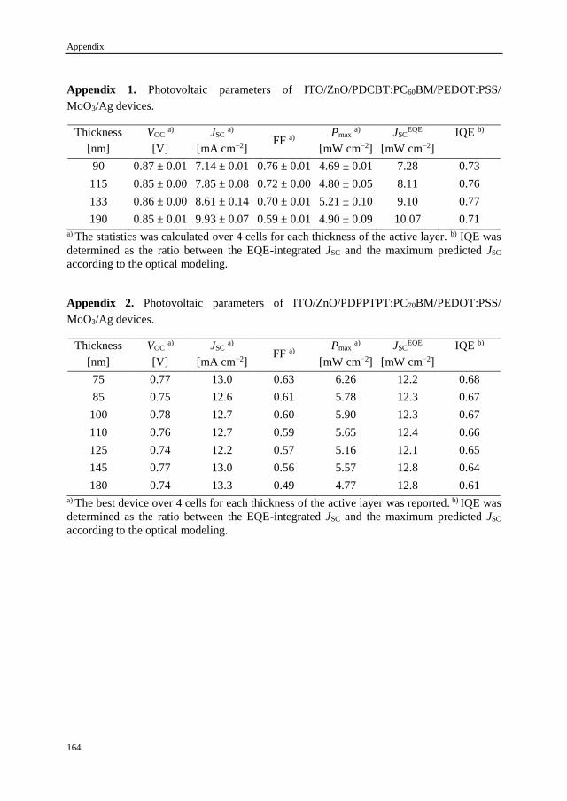
Appendix
164
Appendix 1. Photovoltaic parameters of ITO/ZnO/PDCBT:PC60BM/PEDOT:PSS/
MoO3/Ag devices.
Thickness
[nm]
VOC a)
[V]
JSC a)
[mA cm−2] FF a)
Pmax a)
[mW cm−2]
JSCEQE
[mW cm−2]
IQE b)
90 0.87 ± 0.01 7.14 ± 0.01 0.76 ± 0.01 4.69 ± 0.01 7.28 0.73
115 0.85 ± 0.00 7.85 ± 0.08 0.72 ± 0.00 4.80 ± 0.05 8.11 0.76
133 0.86 ± 0.00 8.61 ± 0.14 0.70 ± 0.01 5.21 ± 0.10 9.10 0.77
190 0.85 ± 0.01 9.93 ± 0.07 0.59 ± 0.01 4.90 ± 0.09 10.07 0.71
a) The statistics was calculated over 4 cells for each thickness of the active layer. b) IQE was
determined as the ratio between the EQE-integrated JSC and the maximum predicted JSC
according to the optical modeling.
Appendix 2. Photovoltaic parameters of ITO/ZnO/PDPPTPT:PC70BM/PEDOT:PSS/
MoO3/Ag devices.
Thickness
[nm]
VOC a)
[V]
JSC a)
[mA cm−2] FF a)
Pmax a)
[mW cm−2]
JSCEQE
[mW cm−2]
IQE b)
75 0.77 13.0 0.63 6.26 12.2 0.68
85 0.75 12.6 0.61 5.78 12.3 0.67
100 0.78 12.7 0.60 5.90 12.3 0.67
110 0.76 12.7 0.59 5.65 12.4 0.66
125 0.74 12.2 0.57 5.16 12.1 0.65
145 0.77 13.0 0.56 5.57 12.8 0.64
180 0.74 13.3 0.49 4.77 12.8 0.61
a) The best device over 4 cells for each thickness of the active layer was reported. b) IQE was
determined as the ratio between the EQE-integrated JSC and the maximum predicted JSC
according to the optical modeling.

Appendix
165
Appendix 3. Photovoltaic parameters of ITO/ZnO/PMDPP3T:PC60BM/MoO3/Ag devices.
Thickness
[nm]
VOC a)
[V]
JSC a)
[mA cm−2] FF a)
Pmax a)
[mW cm−2]
JSCEQE
[mW cm−2]
IQE b)
60 0.64 ± 0.01 10.18 ± 0.10 0.63 ± 0.01 4.05 ± 0.05 10.8 0.69
75 0.63 ± 0.01 12.45 ± 0.19 0.61 ± 0.06 4.72 ± 0.56 13.3 0.70
90 0.62 ± 0.00 14.50 ± 0.18 0.63 ± 0.01 5.66 ± 0.17 15.2 0.70
110 0.61 ± 0.00 15.35 ± 0.20 0.61 ± 0.02 5.74 ± 0.22 15.9 0.70
130 0.61 ± 0.00 15.78 ± 0.21 0.58 ± 0.02 5.58 ± 0.25 16.1 0.70
150 0.60 ± 0.00 15.95 ± 0.24 0.56 ± 0.02 5.29 ± 0.11 16.5 0.71
190 0.59 ± 0.01 15.70 ± 0.47 0.43 ± 0.07 3.98 ± 0.85 16.7 0.71
a) The statistics was calculated over 4 cells for each thickness of the active layer. b) IQE was
determined as the ratio between the EQE-integrated JSC and the maximum predicted JSC
according to the optical modeling.
Appendix 4. Photovoltaic parameters of ITO/PEDOT:PSS/ZnO/PTB7-Th:PC70BM/
PEDOT:PSS/MoO3/Ag devices.
Thickness
[nm]
VOC a)
[V]
JSC a)
[mA cm−2] FF a)
Pmax a)
[mW cm−2]
JSCEQE
[mW cm−2]
IQE b)
80 0.76 ± 0.00 11.78 ± 0.05 0.64 ± 0.01 5.69 ± 0.06 12.0 0.94
110 0.76 ± 0.00 12.20 ± 0.00 0.62 ± 0.01 5.69 ± 0.05 12.7 0.91
125 0.76 ± 0.00 12.93 ± 0.05 0.59 ± 0.01 5.79 ± 0.06 13.3 0.88
130 0.76 ± 0.00 12.73 ± 0.10 0.56 ± 0.00 5.43 ± 0.08 12.9 0.87
140 0.75 ± 0.01 13.53 ± 0.13 0.54 ± 0.01 5.48 ± 0.09 13.9 0.84
160 0.74 ± 0.00 14.23 ± 0.17 0.48 ± 0.01 5.07 ± 0.14 14.3 0.79
170 0.76 ± 0.00 14.80 ± 0.27 0.49 ± 0.01 5.53 ± 0.12 14.9 0.77
a) The statistics was calculated over 4 cells for each thickness of the active layer. b) IQE was
determined as the ratio between the EQE-integrated JSC and the maximum predicted JSC
according to the optical modeling.

Appendix
166
Appendix 5. Photovoltaic parameters of ITO/ZnO/PMDPP3T:PC60BM/PEDOT:PSS/
MoO3/Ag devices.
Thickness
[nm]
VOC a)
[V]
JSC a)
[mA cm−2] FF a)
Pmax a)
[mW cm−2]
JSCEQE
[mW cm−2]
IQE b)
100 0.61 (0.61) 14.8 (14.2) 0.67 (0.67) 6.05 (5.77) 14.4 0.76
120 0.60 (0.60) 14.7 (14.4) 0.66 (0.65) 5.82 (5.59) 14.7 0.76
145 0.60 (0.60) 15.5 (15.2) 0.60 (0.60) 5.58 (5.44) 15.5 0.76
165 0.59 (0.59) 16.1 (15.5) 0.56 (0.55) 5.32 (5.06) 16.1 0.76
175 0.59 (0.59) 17.1 (16.0) 0.55 (0.54) 5.64 (5.13) 16.6 0.76
205 c) 0.59 (0.59) 17.4 (17.0) 0.50 (0.50) 5.13 (4.95) 17.3 0.76
a) For each thickness of the active layer, values for the best cells are reported, average over 4
cells are given in parentheses. b) IQE was determined as the ratio between the EQE-integrated
JSC and the maximum predicted JSC according to the optical modeling. c) The average was
calculated over two devices.
Appendix 6. Photovoltaic parameters of ITO/PEDOT:PSS/ZnO/PDPPSDTPS:PC60BM/
MoO3/Ag devices.
Thickness
[nm]
VOC a)
[V]
JSC a)
[mA cm−2] FF a)
Pmax a)
[mW cm−2]
JSCEQE
[mW cm−2]
IQE b)
60 0.28 (0.27) 7.31 (6.96) 0.52 (0.50) 1.06 (0.94) 7.60 0.48
70 0.26 (0.27) 8.70 (8.56) 0.49 (0.49) 1.11 (1.11) 9.18 0.48
80 0.30 (0.30) 9.99 (9.54) 0.52 (0.52) 1.56 (1.49) 10.19 0.49
120 0.30 (0.30) 12.4 (12.0) 0.48 (0.49) 1.79 (1.75) 12.6 0.51
170 0.32 (0.32) 13.7 (13.0) 0.52 (0.53) 2.28 (2.18) 14.0 0.53
a) For each thickness of the active layer, values for the best cells are reported, average over 2
cells are given in parentheses. b) IQE was determined as the ratio between the EQE-integrated
JSC and the maximum predicted JSC according to the optical modeling.
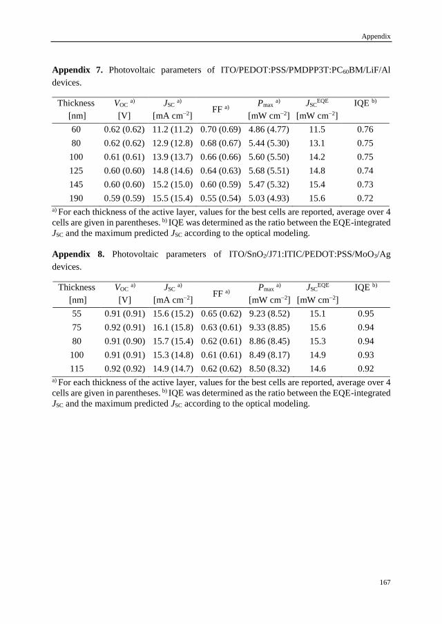
Appendix
167
Appendix 7. Photovoltaic parameters of ITO/PEDOT:PSS/PMDPP3T:PC60BM/LiF/Al
devices.
Thickness
[nm]
VOC a)
[V]
JSC a)
[mA cm−2] FF a)
Pmax a)
[mW cm−2]
JSCEQE
[mW cm−2]
IQE b)
60 0.62 (0.62) 11.2 (11.2) 0.70 (0.69) 4.86 (4.77) 11.5 0.76
80 0.62 (0.62) 12.9 (12.8) 0.68 (0.67) 5.44 (5.30) 13.1 0.75
100 0.61 (0.61) 13.9 (13.7) 0.66 (0.66) 5.60 (5.50) 14.2 0.75
125 0.60 (0.60) 14.8 (14.6) 0.64 (0.63) 5.68 (5.51) 14.8 0.74
145 0.60 (0.60) 15.2 (15.0) 0.60 (0.59) 5.47 (5.32) 15.4 0.73
190 0.59 (0.59) 15.5 (15.4) 0.55 (0.54) 5.03 (4.93) 15.6 0.72
a) For each thickness of the active layer, values for the best cells are reported, average over 4
cells are given in parentheses. b) IQE was determined as the ratio between the EQE-integrated
JSC and the maximum predicted JSC according to the optical modeling.
Appendix 8. Photovoltaic parameters of ITO/SnO2/J71:ITIC/PEDOT:PSS/MoO3/Ag
devices.
Thickness
[nm]
VOC a)
[V]
JSC a)
[mA cm−2] FF a)
Pmax a)
[mW cm−2]
JSCEQE
[mW cm−2]
IQE b)
55 0.91 (0.91) 15.6 (15.2) 0.65 (0.62) 9.23 (8.52) 15.1 0.95
75 0.92 (0.91) 16.1 (15.8) 0.63 (0.61) 9.33 (8.85) 15.6 0.94
80 0.91 (0.90) 15.7 (15.4) 0.62 (0.61) 8.86 (8.45) 15.3 0.94
100 0.91 (0.91) 15.3 (14.8) 0.61 (0.61) 8.49 (8.17) 14.9 0.93
115 0.92 (0.92) 14.9 (14.7) 0.62 (0.62) 8.50 (8.32) 14.6 0.92
a) For each thickness of the active layer, values for the best cells are reported, average over 4
cells are given in parentheses. b) IQE was determined as the ratio between the EQE-integrated
JSC and the maximum predicted JSC according to the optical modeling.
