tapered liga mold insert
TRANSCRIPT

Louisiana State UniversityLSU Digital Commons
LSU Master's Theses Graduate School
2002
Tapered LIGA mold insertRyan Anthony TurnerLouisiana State University and Agricultural and Mechanical College, [email protected]
Follow this and additional works at: https://digitalcommons.lsu.edu/gradschool_theses
Part of the Mechanical Engineering Commons
This Thesis is brought to you for free and open access by the Graduate School at LSU Digital Commons. It has been accepted for inclusion in LSUMaster's Theses by an authorized graduate school editor of LSU Digital Commons. For more information, please contact [email protected].
Recommended CitationTurner, Ryan Anthony, "Tapered LIGA mold insert" (2002). LSU Master's Theses. 1950.https://digitalcommons.lsu.edu/gradschool_theses/1950
TAPERED LIGA MOLD INSERT
A Thesis
Submitted to the Graduate Faculty of the Louisiana State University and
Agricultural and Mechanical College In partial fulfillment of the
requirements for the degree of Master of Science in Mechanical Engineering
in
The Department of Mechanical Engineering
by Ryan Anthony Turner
B.S., Louisiana State University, 2001 December, 2002

Acknowledgements
I will begin by acknowledging my major professor Dr. Kevin Kelly, my mentor
throughout this project, for providing me with the opportunity to study with the
Microsystems group at Louisiana State University. I am grateful for Dr. Kelly’s
motivation, hard work, funding, and guidance which has lead me throughout this process.
I would also like to thank those colleagues who worked along side me under Dr.
Kelly’s supervision: Jian Zhang whose work with SU-8 paved the way for the use of a
reliable photoresist, which was necessary for this project; Jason Tuma for being friend
who was always willing to lend a hand; Adam Cygan for nothing, expect being willing to
laugh; Christophe Marques who’s expansive knowledge of microsystems and all other
subjects was an endless supply of procedures and priceless experience without which the
project would have been nearly impossible; and finally Charles Becnel for being an office
mate and friend who was there the entire time to support, advise, struggle through course
work with, and help in any way to push me towards my goals. Without Chuck my
graduate school experience would have been near unbearable. I will not soon forget the
memorable experiences we shared.
I would like to thank Yohannes Desta and Derrick Mancini for their services and
insight which were integral to the development of this project. Yohannes’ patience and
willingness to help despite his intensely busy schedule were sincerely appreciated. His
services at CAMD were invaluable.
I would like to thank Mezzo Systems for their support of this project including
materials and machine work on the mold insert provided by John Parker. Thanks also
goes out to Paul Rodriguez and his staff for the use of the chemical engineering machine
ii

shop as well as the guidance and support he gave the project during the molding stage.
All parts machined for the overhaul of the injection molding machine were done under
his supervision. These thanks also go out to Emil Geiger and Steve Cortez for their work
in the designing and manufacturing of this overhaul.
I would like to thank Dr. Elizabeth Podlaha and Dr. Jack Helms for serving as
members of my committee. Funding for this project was provided by DARPA (grant
DABT63-99-1-0019). I would also like to thank the State of Louisiana for their support
of the Center for Advanced Microstructures and Devices.
Finally, and most importantly I would like to thank my friends and family whose
support and advice are the most influential factors in my life. Special thanks goes out to
Yogi Barras, Jeremy Bollens, Ryan Greening, Swede Hanson, Chad McCracken, and Ali
Pourmohamadian for giving me godly examples of what friends should be, and providing
support and love in times of need and laughter in times of joy. I would also like to thank
the four most important people in my life: Richard, Peggy, Amy, and Mary Turner. My
family has provided me with unparalleled support and love, and has given me all the
opportunity in the world and a positive environment to succeed.
.
iii
Table of Contents
Acknowledgements……………………………………………………………………...ii
List of Tables…………………………………………………………………………….v
List of Figures………………………………………………………………………...…vi
Abstract…………………………………………………………………………..…….viii
1. Introduction……………………………………………………………………..……..1 1. 1 LIGA………………………………………………………………….……..1 1. 2 Draft Angles in Injection Molding…………………………………….…….2 1. 3 Previous Research on Micromolds with Taper………………………….…..4 1. 4 New Ability to Produce Tapered Features…………………………….…….5 1. 5 Research Goals……………………………………………………….……...7
2. Fabrication…………………………………………………………………….……….9 2. 1 Patterning Tapered Features………………………………………..………..9 2. 2 Pattern Selection……………………………………………………………11 2. 3 Chosen Geometry…………………………………………………………..15 2. 4 X-Ray Mask Fabrication……………………………………………...……17 2. 5 Exposure……………………………………………………………………23 2. 6 Development and Product………………………………………….……….31 2. 7 Electroplating……………………………………………………….………38
3. Molding……………………………………………………………………….………48 3. 1 Injection Molding Machine…………………………………………….…...48 3. 2 Molding Process…………………………………………………….………56
4. Conclusions………………………………………………………………….………..63
Bibliography……………………………………………………………………………..65
Vita………………………………………………………………………………………67
iv

List of Tables
Table 1: Difference in Exposure Times Between PMMA and SU-8……………..…….6
Table 2: Spin Speed vs. Thickness for SU-8 2025……………………………….……20
Table 3: Measurements of Twenty Randomly Selected Posts……………..….…..…...37
Table 4: The Properties of Ticona’s Cyclic Olefin Copolymer…………………….….57
Table 5: Final Molding Parameters for Successful Injection…………..……….……...59
v

List of Figures
Figure 1: Diagram of Vertical vs. Tapered Molding……………………………………3
Figure 2: Draft Angle Effects on the Surface Roughness of a SL………………………5
Figure 3: Normal and Tilted Positions Offered by XRLM-1…………………………...7
Figure 4: Diagram Showing Resulting Pattern from Normal Exposure………………...9
Figure 5: Diagram Showing Resulting Pattern from Tilt and Rotate Exposure……….10
Figure 6: The effects of Four, Six, and Eight Exposures on a Circular Feature……….12
Figure 7: Rotations and Exposed Resists for Square and Hexagonal Patterns…………13
Figure 8: Patterning Geometries for Tapered Exposures………………………………14
Figure 9: The Layout of Posts Showing Face and Corner Spacing Dimensions……….16
Figure 10: The Annulus Formed by the Array of Hexagons…………………………...16
Figure 11: Predicted Feature Dimensions for Patterned Structures…………………….18
Figure 12: The Graphite Substrate with Patterned Resist……………………………....21
Figure 13: The Completed X-Ray Mask………………………………………………..22
Figure 14: The Casting Jig Used to Cast Thick Layers of Photoresist…………………24
Figure 15: The Predicted Geometries Associated with 960 Micron Structures………...26
Figure 16: Three Separate Orientations and Their Resulting Pattern Geometries……...30
Figure 17: Resulting Exposed SU-8 Structures Mounted on the Substrate……………..33
Figure 18: The Top Surface of the Patterned Hexagonal Posts…………………………34
Figure 19: SEM Picture of Patterned Posts (Vertical)…….…………………………….34
Figure 20: SEM Picture of Patterned Posts (Horizontal)……………………………….35
Figure 21: The Resulting Structures From Vertical Wall Exposure…………………….36
Figure 22: Actual and Predicted Geometries of the SU-8 Posts………………………...37
vi

Figure 23: Overplating Nickel to Produce a Mold Insert……………………………….39
Figure 24: The Plating Station Used to Deposit Nickel onto the Substrate…………….41
Figure 25: The Electroplating Jig Used to Support the Stainless Steel Substrate………42
Figure 26: The Electroformed Mold Insert……………………………………………..46
Figure 27: Photographs of the Electroformed Mold Insert……………………………..46
Figure 28: Diagram of a Typical Injection Molding Machine………………………….49
Figure 29: Injection Molding Sequence Steps in Relation to Cycle Time……………..50
Figure 30: Cooling Diagram of the Front Plate………………………………………...53
Figure 31: Diagram Showing the Incomplete Filling Due to Trapped Air……………..54
Figure 32: The Arburg Allrounder 170 CMD Used for Injection Molding…………….55
Figure 33: Platens with Various Systems……………………………………………….55
Figure 34: Molded Part with Incomplete Filling………………………………………..60
Figure 35: The O-rings Being Positioned to Form the Dynamic Seal…………………..61
Figure 36: Final Injection Molded Part………………………………………………….62
vii

Abstract
The applications of microstructures produced by the LIGA process are useful in a
broad range of fields including: microfluidics, heat transfer, and mechanics. The
Microsystems Engineering Team at Louisiana State University has used the LIGA
process as a foundation for the team’s productivity in these areas. Many advances in the
processes involved in producing these microstructures have been made over the past few
years, greatly increasing the efficiency of the entire process. A modified exposure
technique in the lithography stage of the LIGA process is being developed to produce
microstructures with a draft angle as opposed to the standard straight walled structures.
Electroformed mold inserts produced previously have encountered high ejection forces
causing deformation or tearing of the molded products. The tapered sidewalls, produced
by the process outlined in this thesis, are similar to those already used in macro-scale
injection molds, and will dramatically reduce the forces resulting in superior parts with
improved cycle times.
The two objectives that define this research project are: i) to successfully
manufacture a LIGA high aspect ratio microstructure mold insert with tapered features,
and ii) to use the manufactured mold insert and successfully mold and eject parts using a
injection molding machine. A LIGA based mold insert approximately one millimeter in
depth was produced with a three-degree draft angle. This insert was then used with an
injection molding machine to produce and efficiently eject cyclic olefin copolymer
(COC) plastic parts.
viii

1. Introduction
1. 1 LIGA
The Microsystems Engineering Team at Louisiana State University (LSU) has for
the last seven years used a three-step process known as LIGA to successfully produce
microstructures useful in many fields. The first step, X-ray lithography (LI), is used to
pattern a photoresist, usually (poly)methylmethacrylate (PMMA) or SU-8, by the use of
collimated radiation. This radiation changes the molecular pattern in the photoresist,
either by cross-linking the molecular bonds in negative resists (SU-8) or by breaking the
bonds and reducing the molecular weight of a positive resist (PMMA). An x-ray mask
consisting of a pattern of gold absorber features supported by a graphite membrane that is
transparent to x-rays is used to lithographically filter incident radiation onto a sheet of x-
ray sensitive resist that is mounted on a substrate (in our study the substrate is a stainless
steel plate of thickness 0.25 inch). The exposed photoresist is then immersed into a
developing solution, and in the case of a negative resist, the unexposed sections of resist
are removed from the substrate leaving the desired structures behind. For the positive
resist the opposite is true. The exposed resist is removed from the substrate leaving the
untouched resist as the desired microstructures. The second step in the LIGA process is
galvanoformung or electroplating (G). The electrically conductive substrate with the
remaining resist pattern is then placed into an electroplating bath. Metal is deposited
between the voids in the resist structures until the voids are completely filled. Once the
plating fills the voids, the deposition is no longer constrained by the resist features and if
the electroplating process is continued, the features will merge and form a continuous
1

plate that is parallel to the original substrate from which the electroplating process
originated. After the overplated layer becomes sufficiently thick, the electroformed part
is debonded from the original substrate (the bond between substrate and deposited metal
is weak). The resist is removed from the electroformed part and the result is a metal
structure with the negative desired feature pattern built in. The final step in the LIGA
process is abformung (A) or molding. The electroplated metal structure is then used as a
mold insert in one of many processes, including embossing and injection molding. In the
case of injection molding, the part is mounted into the machine and plastic is injected into
the feature pattern and the desired plastic microstructures are produced.
1. 2 Draft Angles in Injection Molding
In the evolution of these processes, many advances have been made to increase
the productivity and usefulness of the LIGA process. One of the most challenging
problems faced in the LIGA process is associated with the molding stage. After molding
plastic into the features of the electroplated mold insert, the part must be ejected or
removed from the mold insert. Failures tend to occur at this point in the process. There is
one main reason for these failures. The radiation provided from the synchrotron is
collimated, and conventional exposure procedures produce straight vertical wall
structures in the photoresist. The result is a mold insert without a taper. Separating the
mold and the part with no taper introduces large ejection forces causing deformations or
tearing in the features[8]. The large ejection forces in straight walled micromolds are due
to the combination of friction and creation of a vacuum while separating the plastic and
the mold [11]. It is widely known that in macro-scale injection molding tapering the
2

sidewalls of the mold will reduce the friction and vacuum forces occurred during
demolding. This is shown in the diagram below.
Figure 1: Diagram of Vertical vs. Tapered Demolding
The amount of draft necessary to avoid friction and vacuum forces is varied
widely from publication to publication. The spectrum of suggested angles ranged from
the minimum of 0.125 degrees [21] to a maximum of five degrees [20]. It should be noted
that the minimum taper angle of 0.125 degrees reported also included that the sidewalls
of the mold must have superior directional finish.
There are several factors in determining the appropriate draft angle for a particular
mold. Higher taper angles are generally preferred to lower ones, but larger taper angles
incur some penalties [8]. As the taper angle increases, the dimensional changes to the
part also increase. One degree of draft creates 0.017” of taper per inch of part length [12].
Another penalty incurred from an exaggerated draft angle is that it requires more product
material per shot thus increasing cost per part. The surface roughness of the sidewall also
needs to be taken into consideration when choosing the appropriate angle. For every
0.001” of texture depth one degree of should be added [12]. Most appropriate taper
angles fall between the ranges of 0.5 and three degrees [5].
3

1. 3 Previous Research On Micromolds with Taper
Tapered micromolds have been built in the past using fabrication procedures other
than deep x-ray lithography. Researchers have studied the effects of draft angle on
stereolithography (SL) injection mold inserts. The SL process starts by creating a
computer-aided design of the mold desired. That design is then sliced into layers and
inputted into a SL machine. The machine uses a platform submerged into a resin bath at a
depth equal to the layer thickness. A laser then cures the resin in the shape of the mold.
The platform then moves further down and the laser cures the next layer until the entire
mold is built. The layer thickness usually ranges from 50 to 200 microns [18].
The results of the research showed that ejection forces were lowered when
employing certain draft angles to the SL molds. In a conventional mold as the draft angle
increased, the ejection forces decreased. However, since SL molds are made in layers,
when applying draft to these molds a stair stepping effect occurs. This stair stepping
effects intensifies the surface roughness of the part. This increased surface roughness
essentially raises the force required to eject the part. Larger draft angles mean a wider
step, which only amplifies this problem. Figure 2 shows two different draft angles for an
SL mold. In the figure the layer thickness of the two parts are equivalent.
In the research it was concluded that increasing the draft angle does not
necessarily assist in the ejection of the part [4]. A balance was needed between the
surface roughness and draft angle. In order for draft angles to be used effectively in SL
micromolds an optimization between draft angles and layer thickness needs to be
performed. This would ensure a minimized ejection force.
4
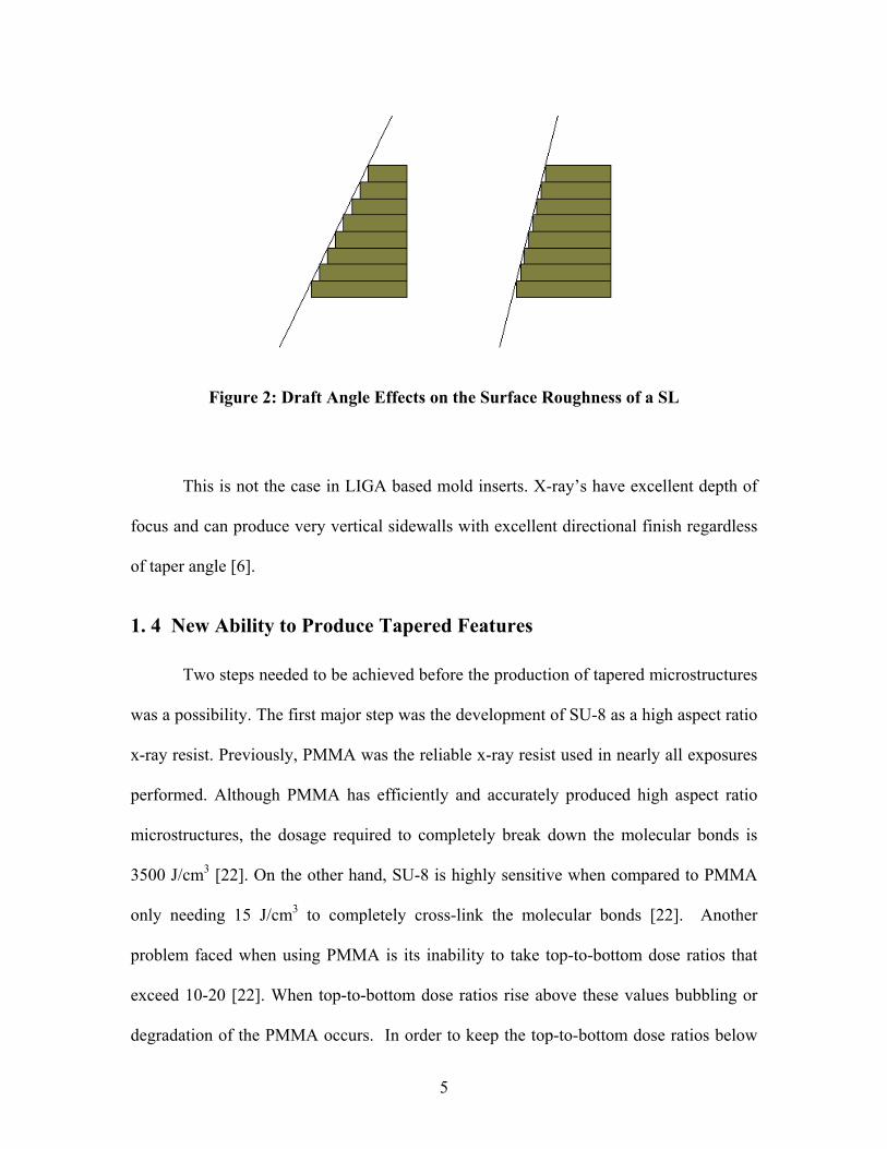
Figure 2: Draft Angle Effects on the Surface Roughness of a SL
This is not the case in LIGA based mold inserts. X-ray’s have excellent depth of
focus and can produce very vertical sidewalls with excellent directional finish regardless
of taper angle [6].
1. 4 New Ability to Produce Tapered Features
Two steps needed to be achieved before the production of tapered microstructures
was a possibility. The first major step was the development of SU-8 as a high aspect ratio
x-ray resist. Previously, PMMA was the reliable x-ray resist used in nearly all exposures
performed. Although PMMA has efficiently and accurately produced high aspect ratio
microstructures, the dosage required to completely break down the molecular bonds is
3500 J/cm3 [22]. On the other hand, SU-8 is highly sensitive when compared to PMMA
only needing 15 J/cm3 to completely cross-link the molecular bonds [22]. Another
problem faced when using PMMA is its inability to take top-to-bottom dose ratios that
exceed 10-20 [22]. When top-to-bottom dose ratios rise above these values bubbling or
degradation of the PMMA occurs. In order to keep the top-to-bottom dose ratios below
5

ten, aluminum filters are used to filter out the low energy radiation. Unfortunately, this
causes the exposure time of the PMMA to increase. Again, SU-8 tends to outperform
PMMA, as it has shown to not be as prone to the top-to-bottom dose ratio problems such
as bubbling. This equates to a tremendous difference in the amount of time it takes to
expose the two x-ray resists. The table below provides a few examples of the exposure
times for PMMA and SU-8, respectively. The times are calculated for four different
resist thicknesses. The thickness of the aluminum filter needed to keep the dose ratio
below ten for the PMMA is also given, and a six micron aluminum filter was used for all
thicknesses of the SU-8. The radiation source used for the calculations of exposure times
was the synchrotron ring located at the Center for Advanced Microstructure Devices
(CAMD) in Baton Rouge, Louisiana.
Table 1: Difference in Exposure Times Between PMMA and SU-8
Resist SU-8 Exposure PMMA Exposure Aluminum Filter
Thickness Time (minutes) Time (minutes) Thickness for PMMA
2000 microns 13.7 5947 50 microns
1500 microns 8.4 2959 30 microns
1000 microns 4.4 1143 10 microns
500 microns 1.9 352 no filter
The modified LIGA process that is required to produce tapered microstructures is
difficult using PMMA. In producing tapered microstructures multiple exposures are used
to produce the desired patterns. Multiple exposure lithography using PMMA is
problematic for two reasons. The time of exposure for producing tall (1mm- 2mm)
microstructures would prove unfeasible, when compared to the time it would take to
expose the SU-8. Secondly, when calculating top-to-bottom dose ratios, the effective
6

dose ratio for a single exposure must be multiplied by the number of exposures desired.
Multiple exposures would simply exceed the acceptable value for top-to-bottom dose
ratios. SU-8 properties fit the requirements that stem from a tapered LIGA exposure.
The second major step that made the production of tapered microstructures
possible was the acquisition of a new x-ray lithography beamline at CAMD. The new
beamline, named XRLM-1, has modified features, which include tilt and rotate
capability, necessary to perform the tapered exposure. XRLM-1 allows the substrate
(with photoresist) and mask to tilt at an angle to the vertical position. While tilted, the
substrate and mask can rotate 360 degrees around that angle. The figure below shows
both the normal and tilted positions.
Figure 3: Normal and Tilted Positions offered by XRLM-1
1. 5 Research Goals
The introduction of a taper into a LIGA based mold insert has never been
attempted. Based on the information presented previously, these inserts have the potential
7
to greatly increase the efficiency and productivity of the molding process. These reasons
prove the interest for research into the development and use of tapered mold inserts.
There were two main objectives set forth for the following research. The first goal
was to successfully manufacture a LIGA high aspect ratio microstructure mold insert
with tapered features. This process includes all steps of the manufacturing process. The
second goal of the research was to use the manufactured mold insert and successfully
mold and eject parts using an injection molding machine. The successful completion of
these two goals will aid in the advancement of the entire LIGA process.
Through the rest of this thesis, the steps taken to achieve these goals and the
corresponding results will be presented. Chapter II will describe the manufacturing
process used to fabricate the tapered mold insert. It will first describe the modified LIGA
process used, followed by descriptions of the pattern selection, building of the x-ray
mask, exposing the sample, electroplating, and finally the SU-8 burnout. Chapter III will
discuss the completion of the second goal, molding and ejecting the plastic parts from the
injection molding machine. This includes the fabrication of an ejection system to
complement the injection molding machine, mold insert mounting, selection of plastic
and corresponding parameters, and results obtained. The conclusion of the results and
further investigations needed is presented in Chapter IV.
8

2. Fabrication
2. 1 Patterning Tapered Features
Tapered features are created in the photoresist by a tilt and rotate feature on the
beamline. During a normal exposure, mask and substrate are oriented vertically, 90
degrees to the incoming horizontal radiation provided by the synchrotron. During the
exposure, the mask and substrate move up and down over the entire scan length to expose
the complete pattern. This produces the normal vertical sidewalls in the desired
structures. A diagram of this is shown below.
Figure 4: Diagram Showing Resulting Pattern from Normal Exposure
In order to create the desired taper pattern the mask and substrate are tilted
relative to the incoming radiation. The tilt enables the incoming collimated radiation to
expose photoresist "under" the gold absorber pattern. This produces a slanted exposed
feature in the photoresist. When the tilt is performed in addition with rotation, it allows
the radiation to penetrate the photoresist at all angles under the absorber, thus creating a
9
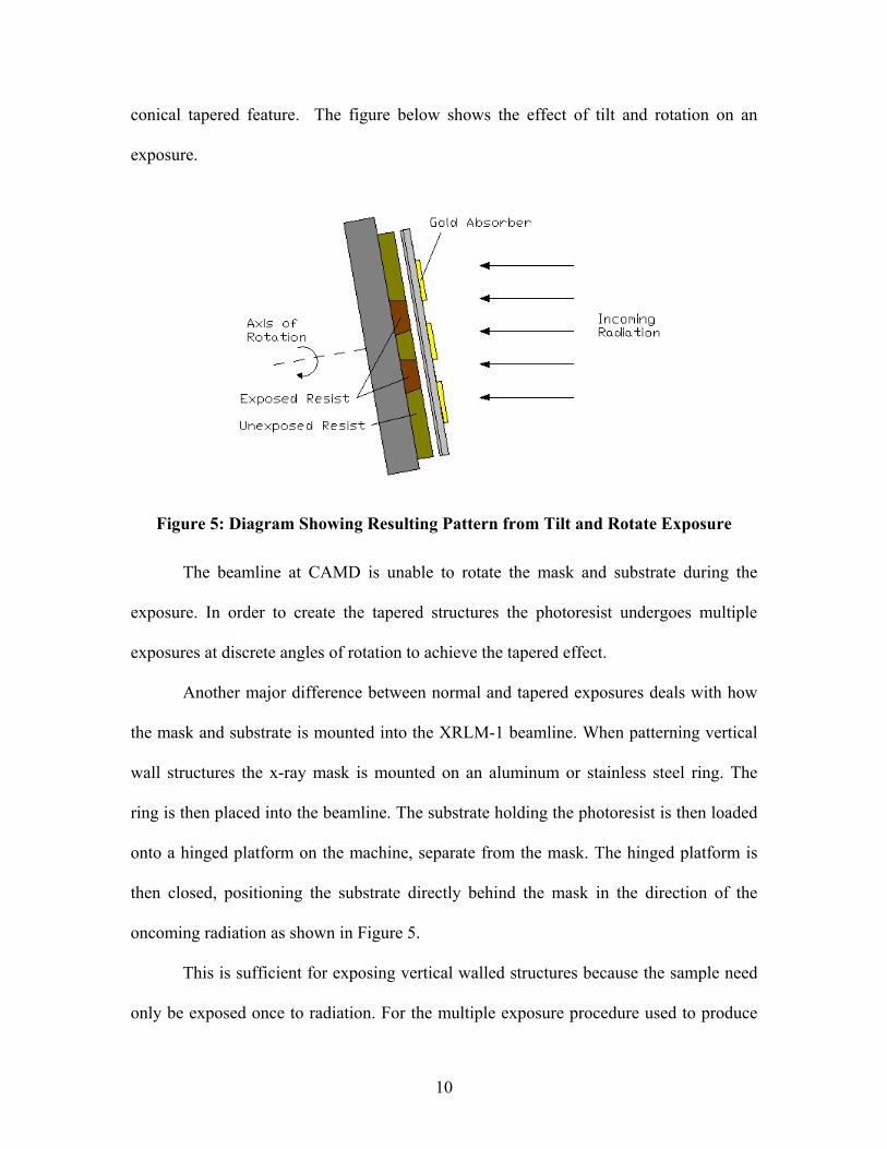
conical tapered feature. The figure below shows the effect of tilt and rotation on an
exposure.
Figure 5: Diagram Showing Resulting Pattern from Tilt and Rotate Exposure
The beamline at CAMD is unable to rotate the mask and substrate during the
exposure. In order to create the tapered structures the photoresist undergoes multiple
exposures at discrete angles of rotation to achieve the tapered effect.
Another major difference between normal and tapered exposures deals with how
the mask and substrate is mounted into the XRLM-1 beamline. When patterning vertical
wall structures the x-ray mask is mounted on an aluminum or stainless steel ring. The
ring is then placed into the beamline. The substrate holding the photoresist is then loaded
onto a hinged platform on the machine, separate from the mask. The hinged platform is
then closed, positioning the substrate directly behind the mask in the direction of the
oncoming radiation as shown in Figure 5.
This is sufficient for exposing vertical walled structures because the sample need
only be exposed once to radiation. For the multiple exposure procedure used to produce
10

tapered features, this procedure is unacceptable. In the setup mentioned above, the mask
and substrate are mounted separately allowing them to move with respect to one another.
After each exposure XRLM-1 goes through a realignment stage before a new exposure
can be performed. The beamline moves the two separated pieces and then attempts to
realign them. Unfortunately, the realignment is not highly accurate and causes the
following exposure to be off center, ruining the exposure. In order to remedy this
problem, the mask is mounted directly to the substrate to eliminate the possibility of
relative movement between the two. The substrate is then mounted to the hinged
platform, and the previous fixture used to bind the mask is left empty. The platform is
then positioned into place in the same manner as the normal exposure.
2. 2 Pattern Selection
In designing useful microstructures a wide variety of shapes and patterns emerge.
Different shapes need to undergo the appropriate amount of exposures to ensure the best
tapered pattern. Circles, squares, and hexagons are common shapes for fields of posts.
Circles, for instance, would produce the best taper under a continuously rotating setup.
Since the beamline lacks this feature, the best case for circles would be to expose the
sample as many times as possible without suffering from radiation leaking through the
mask. Using the multiple exposure process, a perfect tapered circle is not attainable. The
final patterned structure resembles the form of a flower. As the number of exposures
increases, the petals of the flower seem to overlap each other making the exposed resist
more circular. The figure below shows the difference between four, six, and eight
exposures on a circular pattern. The yellow center represents the mask, and the brown
outer rim makes up the areas of exposed resist.
11

Figure 6: The Effects of Four, Six, and Eight Exposures on a Circular Feature.
Unlike circles, squares and hexagonal features can be patterned to perfect
tapered square and hexagonal structures. A four step multiple exposure can produce the
desired results for a square, and a six step procedure is required for hexagons. In
patterning the square, the mask is orientated so that one of the corners of the squares
points upwards. This is necessary in order for the tapered pattern to remain a perfect
square. Allowing the mask to be shifted either way would result in gaps or missing
sections in the exposed resist. The sample is oriented and exposed four times, rotating
ninety degrees between each exposure to complete the tapered square structure. The
concepts that apply to the square features also apply to the hexagonal features. Again, it
is essential to position the mask with a corner pointing up to ensure a complete hexagonal
structure. The hexagonal patterns are exposed six times, rotating the sample sixty degrees
each time. The figure below shows the individual exposures for the square and hexagonal
patterns. The brown area shows where the photoresist is exposed in each exposure. The
orange areas are the previously exposed resist, and the shapes in yellow represent the
mask used. The number 1 references how the mask and substrate were rotated.
12

Figure 7: Rotations and Exposed Resists for Square and Hexagonal Patterns
The modified exposure process used to pattern tapered structures in SU-8 placed a
new importance on the distance between the mask and substrate. This distance or gap
becomes a crucial element to the resulting patterned structure in the photoresist. As it was
discussed previously, in vertical wall exposures the mask and substrate were aligned
together by means of a hinged platform positioning the substrate directly behind the
mask. The gap in vertical wall exposures was not extremely important, and was
controlled by adding a spacer, anywhere from 100-1000 microns, between the two parts.
This is not true of tapered exposures. Unlike vertical wall exposures, the resulting resist
feature geometry is heavily dependent on the gap between the mask and
substrate/photoresist. As the distance between the two increases, the area of resist
exposed becomes larger and larger increasing the size of the patterned structures. This
fact requires that the gap size be controlled precisely in order to produce structures with
the desired features. The relationship between gap size and the resulting patterned
structure is governed by the simple geometric derived equation given in Equation (1)
below:
13

( ) ( GapzDzD m +∗∗+= )θtan2)( Equation 1
where:
D(z) = the feature dimension as a function of distance, z, beneath the SU-8 surface
Dm = the mask dimension allowing X-rays through
θ = the desired taper angle
Gap = the distance between the mask absorber features and the SU-8
Z = the distance below the SU-8 surface
Figure 8: Patterning Geometries for Tapered Exposures
According to the equation above for patterning structures with a three degree draft
angle, every ten microns in gap size relates to about one micron in width increase of the
patterned structure. The gap between the mask and substrate must be controlled in order
to achieve the desired results.
14

2. 3 Chosen Geometry
A field of posts was chosen for the tapered exposures. This field of posts forms a
pattern which is used currently for developing a seal with the posts aiding in the heat
transfer from the body of the seal. The posts are hexagonal in shape, and the field of posts
form a circular annulus.
The pattern was selected for several reasons. One reason was the desire to
fabricate tapered features for a pattern the Microsystems Team is currently using to
develop a part. This would allow for the further development of a project, and show the
impact that tapered features would have. A more important reason for the selection of the
seal pattern, however is that it has the appropriate feature dimensions for the tapered
exposure. The hexagons are relatively large when compared to most structures patterned
in microsystem design. Each hexagon measures 276 microns between parallel faces, and
298 microns between opposite points of the hexagon. (the sidewall length of the
hexagons equals 160 microns). The hexagons are also spaced far enough apart to ensure
that the tapering posts do not overlap near the substrate where the posts are widest. The
extra spacing also allows for easier development of the unexposed SU-8. Each row of
hexagons are shifted one half section forming a honeycomb, so that every face of an
interior hexagon is parallel to the face of its neighboring hexagon. Each feature is
separated by a measure of 400 microns from parallel face to parallel face. Figure 9 below
lays out the honeycomb pattern of the hexagons. In the diagram the letter F represents the
distance from face to face (276 microns), C represents the corner to corner measurement
(298 microns), and H represents the distance of separation between the features.
15
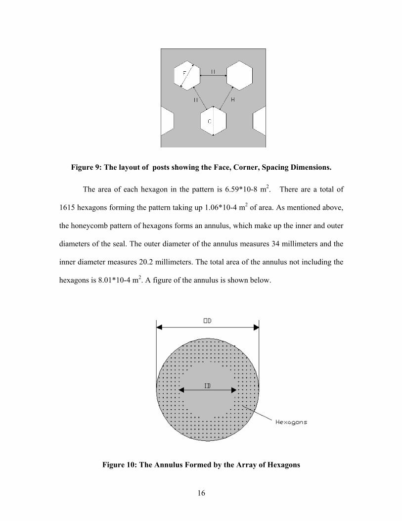
Figure 9: The layout of posts showing the Face, Corner, Spacing Dimensions.
The area of each hexagon in the pattern is 6.59*10-8 m2. There are a total of
1615 hexagons forming the pattern taking up 1.06*10-4 m2 of area. As mentioned above,
the honeycomb pattern of hexagons forms an annulus, which make up the inner and outer
diameters of the seal. The outer diameter of the annulus measures 34 millimeters and the
inner diameter measures 20.2 millimeters. The total area of the annulus not including the
hexagons is 8.01*10-4 m2. A figure of the annulus is shown below.
Figure 10: The Annulus Formed by the Array of Hexagons
16

The predicted feature geometry of the final molded product was then determined
by setting three parameters: Photoresist (SU-8) thickness, Draft Angle, and Gap Size. The
resist thickness was set at one millimeter. One millimeter was an appropriate height for a
six-sided tapered exposure because it would provide a sample with a high aspect ratio,
yet would be easily penetrated by the x-ray radiation minimizing the effect of radiation
leakage through the mask. A draft angle of three degrees was chosen for the tapered
structures. Three degrees was selected, according to the literature gathered, as a high
taper angle for molds with exceptional directional finish. The three degree taper angle
also does not severely affect the dimensional integrity of the part, and will provide an
adequate reduction in ejection forces during the molding stage. The gap size was set at
380 microns. The gap size was minimized in order to keep the feature dimensions of the
hexagons as small as possible. The hexagons were already relatively large, and as the gap
size increased the feature dimensions increased as well. Using Equation 1, and the
parameters given above the predicted feature dimensions were calculated and are
presented in the figure below. Because of the gap, the dimension between parallel faces
would increase from 278 microns to 316 micrometers. The corresponding base
dimension is predicted to be 421 micrometers.
2. 4 X-ray Mask Fabrication
The purpose of the X-ray mask is to filter the incoming collimated radiation into a
desired pattern before it strikes the photoresist. The mask consists of a thin graphite
substrate with the desired pattern drawn out by gold. The gold is used as an absorber to
filter out the undesired radiation.
17

Figure 11: Predicted Feature Dimensions for Patterned Structure (units in microns)
Although gold is quite effective in filtering radiation, the x-rays are powerful
enough to penetrate the gold. This radiation leakage poses extra problems for the
processes associated with tapered exposures. Since the exposures are performed using the
relatively sensitive SU-8 photoresist, leakage is a serious problem. This problem is
compounded by the fact that producing tapered structures requires multiple exposures.
Fortunately, as the thickness of the gold increases, its ability to filter the radiation also
increases. These problems are solved by ensuring that the gold absorbers are thick
enough to filter out the undesired radiation, making sure the SU-8 does not receive the 15
J/cm3 dose it needs to cross-link.
A Microsoft Excel spreadsheet program, which uses as inputs the radiation energy
of the synchrotron and the thickness and densities of various filters, is used to calculate
the dose delivered to the photoresist. By entering an extra layer of gold as a filter the
program can calculate the amount of radiation that is able to leak through the gold
absorbers. The density of gold is 19.3 grams per cubic centimeter. It was decided, based
on the parameters selected for the tapered exposure, that 30 microns of gold would be
18
sufficient for blocking out the undesired radiation. For each exposure the SU-8 resist
would receive a dose of 1.61*10-2 J/cm3 in the undesired regions. For all six exposures
the total would equal 9.66*10-2 J/cm3 far less than is needed for cross-linking to occur.
The x-ray mask is fabricated by the use of UV lithography. The process starts by
creating a CAD drawing of the desired pattern. After the pattern is completed, the
creation of a UV mask is the first step in making the x-ray mask. A glass square with a
chromium layer is covered with a thin layer of resist. The CAD drawing is uploaded into
a machine, which patterns the resist. The undesired resist is removed and the piece is
subjected to a chromium etching process that removes the exposed chromium. The resist
is then removed revealing a patterned chromium film. The chromium acts as an absorber
to UV light in the same way that the gold blocks the x-ray radiation.
The foundation of the x-ray mask is the graphite substrate. The graphite has a
density of 1.8 grams per cubic centimeters. The sheets of graphite are 320 microns thick
and are cut into five-inch circles. The preparation of the graphite begins by mounting the
disk to plate of glass in the same shape. The graphite is then sanded down directionally
using water as a lubricant in order to prepare the surface. Three stages are completed with
sandpaper of grits 240, 400, and 600. After being cleaned and dried, the mounted graphite
is then coated with a negative photoresist by the use of a Biotec SP100 spin coater. The
photoresist used was SU-8 2025, capable of spinning to resist thicknesses between 80 and
25 microns. The resist was spun onto the graphite for thirty seconds at 1500 revolutions
per minute. This process produced an even coat of SU-8 2025 at a thickness of fifty
microns. The fifty microns of SU-8 was needed in order to make gold structures to the
required thirty microns in height. After spinning, the graphite was allowed to sit on an
19
even surface for ten minutes to let the resist settle. The spin chart for SU-8 2025 is shown
in the table below.
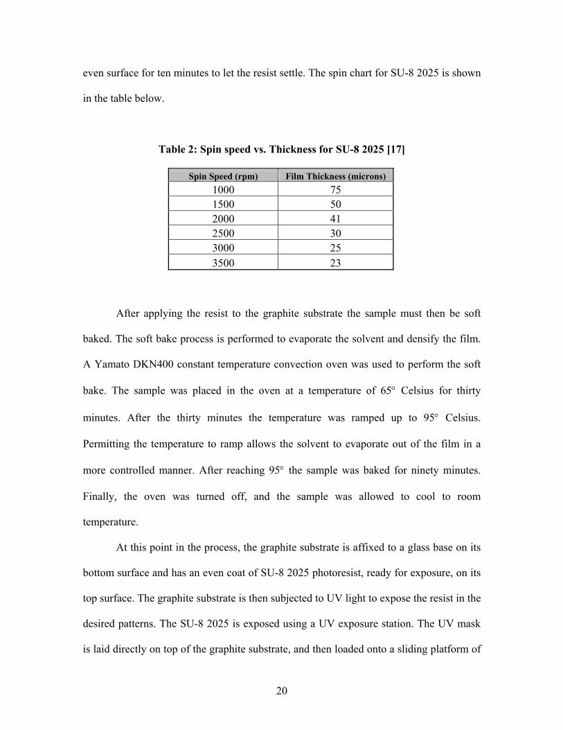
Table 2: Spin speed vs. Thickness for SU-8 2025 [17]
Spin Speed (rpm) Film Thickness (microns) 1000 75 1500 50 2000 41 2500 30 3000 25 3500 23
After applying the resist to the graphite substrate the sample must then be soft
baked. The soft bake process is performed to evaporate the solvent and densify the film.
A Yamato DKN400 constant temperature convection oven was used to perform the soft
bake. The sample was placed in the oven at a temperature of 65° Celsius for thirty
minutes. After the thirty minutes the temperature was ramped up to 95° Celsius.
Permitting the temperature to ramp allows the solvent to evaporate out of the film in a
more controlled manner. After reaching 95° the sample was baked for ninety minutes.
Finally, the oven was turned off, and the sample was allowed to cool to room
temperature.
At this point in the process, the graphite substrate is affixed to a glass base on its
bottom surface and has an even coat of SU-8 2025 photoresist, ready for exposure, on its
top surface. The graphite substrate is then subjected to UV light to expose the resist in the
desired patterns. The SU-8 2025 is exposed using a UV exposure station. The UV mask
is laid directly on top of the graphite substrate, and then loaded onto a sliding platform of
20

the UV exposure station. The light is directed straight down towards the mask, is filtered,
and then exposes the resist. The required dose for patterning fifty microns of SU-8 is 300
mJ/cm2 [17]. The station emits UV light at a rate 30 mJ/cm2*sec. To completely expose
the sample the SU-8 was exposed for ten seconds. Following the exposure, the sample is
post baked to cross-link the exposed resist. As in the soft bake, the temperature must be
ramped to the appropriate levels to minimize stress and avoid resist cracking [17]. The
sample is placed into the convection oven for post baking at a temperature of 65º Celsius
for thirty minutes. The temperature is then ramped to 95º and held for sixty minutes.
After the bake, it is then cooled to room temperature, and left on a flat surface for six
hours to settle. When the settling period is completed, the unexposed resist is removed
from the substrate by using an SU-8 developing solution. The sample is immersed face
down in the solution on supports allowing for agitation from a magnetic stirrer bar. With
stirring, the sample was left in the developing solution for twenty-five minutes to allow
for the complete removal of the unexposed resist. After development, the graphite
substrate with the patterned resist was cleaned first with isopropyl alcohol (IPA), and
then deionized (DI) water. The sample was then gently air-dried. A picture of the graphite
and the resist patterned is shown in Figure 12.
Figure 12: The Graphite Substrate with Patterned Resist
21

After debonding the graphite substrate from its glass base, the sample was ready
for the final process. The next stage in completing the x-ray mask was to electroplate
gold onto the graphite substrate to a height of thirty microns. The desired pattern only
required that gold be plated inside of the circle near the posts. To prevent gold from being
plated outside of the outer diameter of the pattern an electroplating tape was used to
cover all of the conductive sections of the substrate in that area. The sample was sent to
CAMD where it was placed into a gold electroplating bath. To prepare the sample, it is
placed into a beaker of deionized water, and vacuumed to remove air that is trapped in
the features. The sample is then placed into the bath for plating. The bath is a Techni-
Gold 25E solution from Technic Inc. with a pH set between 6-7. The temperature of the
bath is kept at a steady 43° Celsius, and the gold electroplating is done in pulses set at
40Hz. The current density is for plating gold is 1 mA/cm2. The gold is electrodeposited
onto the substrate at a rate of 3.7 microns per hour. This process takes approximately
eight hours to plate thirty microns of gold. The following picture shows the completed x-
ray mask with the plated gold absorbers.
Figure 13: The Completed X-ray Mask
22

2. 5 Exposure
The deep x-ray exposure into the one-millimeter of SU-8 begins with the
preparation of the substrate with the affixed photoresist. The substrate is made of a disk
of stainless steel. The disk thickness ranges from 6-7 millimeters, and is 4.75 inches in
diameter. The top surface of the plate is turned down on a lathe to a level finish within
0.002 of an inch. The surface is then sandblasted. Throughout the exposure process the
photoresist can develop highly stressed areas caused by shrinking. This tendency
sometimes results in the resist debonding from the substrate. The sandblasting helps the
SU-8 adhere to the stainless steel by giving it a gritty surface helping to prevent the
lateral shifting caused by shrinking and giving it more surface area to bond to. The
stainless steel substrate is now ready for the application of the thick layer of SU-8 2075.
In order to obtain thick layers (500 µm- 2500 µm) of SU-8 a casting process is
employed rather than the usual spin coating method. The substrate is thoroughly cleansed
with soap and water, and then dried in the convection oven for twenty minutes at 85°
Celsius. A special casting jig is used to cast the resist onto the substrate. The setup is
equipped with an aluminum bottom plate bored out to the outer diameter of the substrate.
The substrate is placed into the bored out section of the bottom plate. A top plate with a
four inch circle cut out of its middle sandwiches a four inch plastic ring against the
substrate. This plastic ring and the substrate define the volume into which the photoresist
will be cast. The top plate is then bolted to the bottom plate to apply pressure between the
ring and the substrate to prevent the resist from leaking. The casting process requires
heating the photoresist for extended periods of time. To accomplish this, two heaters are
embedded in the bottom plate of the jig just below the substrate to maintain the required
23

temperature (105° C) throughout the casting process. The heaters are connected to a
solid-state relay and temperature controller to maintain a constant casting temperature. A
picture of the casting jig is shown below.
Figure 14: The Casting Jig Used to Cast Thick Layers of Photoresist
After the substrate is cleaned, dried, and loaded into place, the casting jig is
heated to 105° Celsius. The SU-8 2075 is then measured out using a graduated cup to the
required volume needed to cast the desired thickness of the resist. In order to cast a resist
thickness of one millimeter, 15 milliliters of SU-8 2075 is needed. After the appropriate
amount of resist is measured, it is poured through the four-inch circle of the top plate of
the jig, directly onto the substrate. The top plate is then covered with a glass plate to
prevent dust or any other particles from falling into the casting resist. The entire jig is
then covered with aluminum foil to prevent any light from prematurely exposing the
resist. The casting process requires twenty hours at 105° Celsius to harden the SU-8
24
2075. After the casting period is over and the SU-8 resist has hardened, the casting jig
heaters are turned off. The sample is allowed to cool to room temperature in the jig.
When the sample has cooled, the substrate is removed from the jig. The four-inch
diameter plastic ring remains affixed to the substrate. The plastic ring is removed from
the substrate by the use of a lathe.
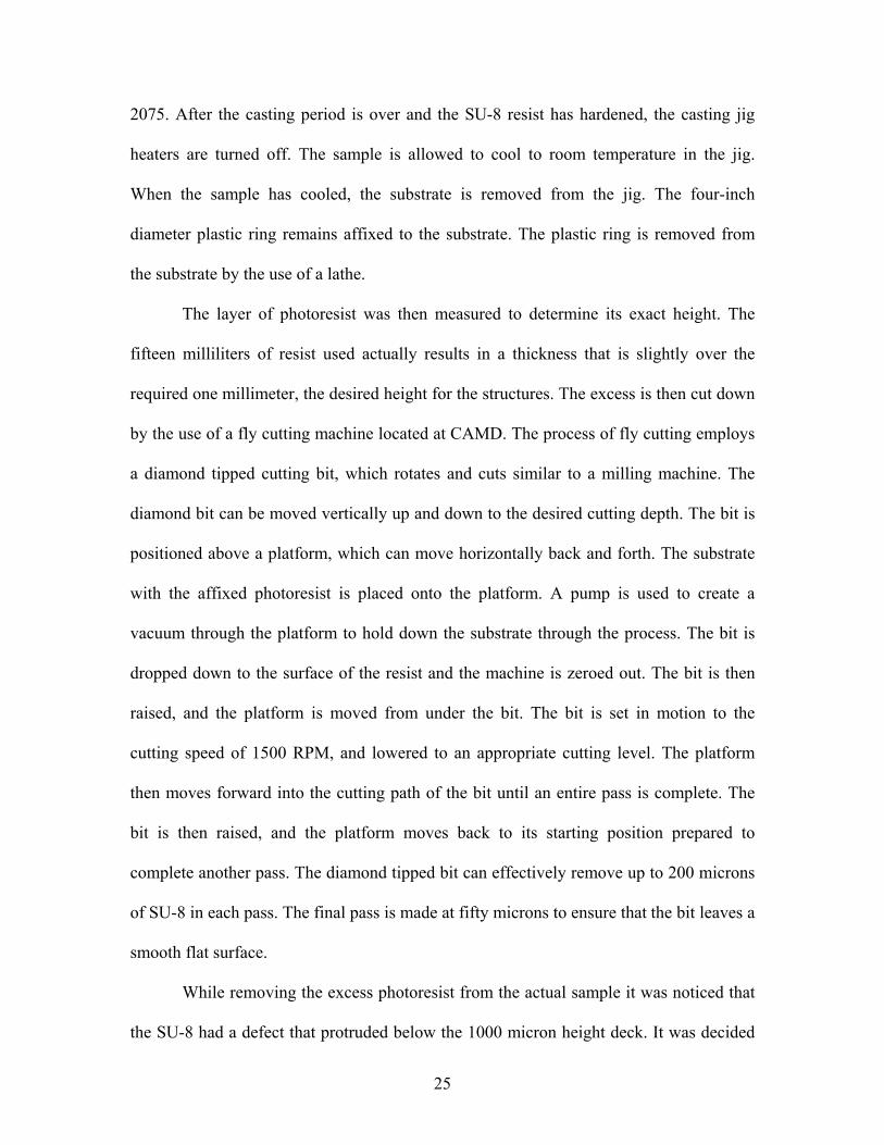
The layer of photoresist was then measured to determine its exact height. The
fifteen milliliters of resist used actually results in a thickness that is slightly over the
required one millimeter, the desired height for the structures. The excess is then cut down
by the use of a fly cutting machine located at CAMD. The process of fly cutting employs
a diamond tipped cutting bit, which rotates and cuts similar to a milling machine. The
diamond bit can be moved vertically up and down to the desired cutting depth. The bit is
positioned above a platform, which can move horizontally back and forth. The substrate
with the affixed photoresist is placed onto the platform. A pump is used to create a
vacuum through the platform to hold down the substrate through the process. The bit is
dropped down to the surface of the resist and the machine is zeroed out. The bit is then
raised, and the platform is moved from under the bit. The bit is set in motion to the
cutting speed of 1500 RPM, and lowered to an appropriate cutting level. The platform
then moves forward into the cutting path of the bit until an entire pass is complete. The
bit is then raised, and the platform moves back to its starting position prepared to
complete another pass. The diamond tipped bit can effectively remove up to 200 microns
of SU-8 in each pass. The final pass is made at fifty microns to ensure that the bit leaves a
smooth flat surface.
While removing the excess photoresist from the actual sample it was noticed that
the SU-8 had a defect that protruded below the 1000 micron height deck. It was decided
25

that the photoresist was to be machined down below the affected area of the SU-8. The
passes were made at smaller increments until the blemish was removed. The final height
of the SU-8 photoresist was 960 microns tall. The change in thickness of the resist
affected the predicted geometries of the patterned structures. The forty micron difference
in height still provided structures with a high aspect ratio. The gap size of 380 microns
remained the same, as well as the three degree draft angle. Coupling these two parameters
with the new height of the SU-8 did not compromise the integrity of the design. Taking
into consideration that the only changing parameter was the height of the resist, it can be
seen that the only changed dimension besides the height of the structure was at the
bottom of the structure at the substrate. The new predicted bottom dimension between the
parallel faces of the hexagon was 416 microns, five less than the previous 421 microns.
The predicted patterned structure is shown below.
Figure 15: The Predicted Geometries Associated with 960 Micron Structures
Once the x-ray mask and the prepared substrate were completed, the process of
patterning the structures into the photoresist using the synchrotron at CAMD began. The
26

process begins with calculating the required exposure dose to completely cross link the
SU-8 in the desired regions. The dose calculations are performed using the spreadsheet
program mentioned before in calculating the desired thickness of the gold absorber. The
program uses the incoming radiation energy and the densities and thicknesses of the
various filters, including the resist, to calculate the energy absorbed by the SU-8. The
filters for the tapered exposure performed included a beryllium filter, a kapton filter, the
graphite of the mask, and the photoresist being patterned. XRLM-1, the beamline with
the tilt and rotate capabilities, has a beryllium filter located inside of the x-ray
lithography machine. The beryllium filter has a thickness of 200 microns and a density of
1.83 grams per cubic centimeter. The radiation was then passed through a kapton
(C22H10N205) filter. The kapton has a thickness of 60 microns, and a density of 1.43
grams per cubic centimeter. The graphite substrate of the x-ray mask also serves as a
filter. The graphite has a density of 1.8 grams per cubic centimeter, and as mentioned
before, was 320 microns thick. The final filter that is included in the dose calculations is
that of the photoresist. The SU-8 has a density of 1.19 grams per cubic centimeter at a
thickness of 960 microns. There are two more values associated with calculating the
required dose for the exposure: the ring energy and the dose. The ring energy of the
XRLM-1 beamline is 1.3*109 electron volts or 1.3 GeV. The dose was set to 15 J/cm3,
the value needed to cross-link the SU-8 resist. The values were loaded into the
spreadsheet program to calculate the exposure dose. The required dose to pattern the SU-
8 at the bottom surface was 109.96 milliamp minutes per centimeter.
The calculation of the required exposure dose completed the background work
necessary to pattern the tapered structures. The x-ray mask, substrate with resist, and the
exposure doses were brought to CAMD for the x-ray lithography process. When the
27

beamline became available, it was then prepared for the tilt and rotate procedure. The
hinged platform in which the substrate is affixed was unlatched and moved into the
loading position. The substrate was then ready to be loaded into the machine. This
process was done swiftly to reduce the possible exposure to UV light. From the
beginning of the handling process, the SU-8 was shielded from any source of UV
radiation to prevent premature reaction in the photoresist. The SU-8 comes in a protected
bottle, and is handled in the laboratory under the security of UV filtered light during the
casting process. When transporting the substrate with the unexposed resist, aluminum foil
is used to safeguard against the sun’s radiation, and from any unfiltered UV light from
artificial light indoors. Unfortunately, the light inside of CAMD near the beamlines is not
filtered for UV radiation. The sensitive nature of the SU-8 photoresist necessitates a swift
loading process to minimize the amount of radiation the resist is exposed to.
Now that the hinged platform was ready and in the loading position, the substrate
with the unexposed resist was unwrapped from its aluminum foil shield. The substrate
was placed with the resist facing upwards onto the loading deck. Three allen bolts were
then used to affix the substrate to the deck. The x-ray mask was then prepared to be
loaded into the machine. For a standard vertical wall exposure, the x-ray mask is mounted
onto a designated ring. A removable fixture designed to hold the mask and ring is then
taken out of the machine. The mask is loaded onto the fixture, and the assembly is loaded
back into the machine in what will be path of the oncoming collimated radiation. At that
point the hinge is closed positioning the photoresist and substrate directly behind the
mask. However for the tapered structures, in order to prevent the mask and substrate from
moving relative to each other in between individual exposures, the mask has to be
directly connected to the substrate. At this point in the process the substrate was loaded
28

onto the hinge with the resist facing upwards. A sheet of kapton sixty microns thick was
placed directly over the substrate. The kapton was cut into a square sheet that completely
covered the thick layer of resist on the substrate. The x-ray mask is then taken from its
case, and laid directly on top of the kapton sheet. Tape with a strong adhesive was then
used to secure the mask and the kapton filter to the substrate. Now the vertical loading
deck held the substrate, kapton, and mask securely fastened to avoid the relative
movement between the mask and substrate.
The orientation of the mask is very important to the final patterned product. When
patterning hexagons, the mask must be positioned so that one of the hexagons six points
faces directly up. Any fluctuation from this orientation will produce slight gaps in the
patterned structure. The figure below shows three different orientations, their resulting
patterned structure as viewed form the top. Two of the orientations are off center and as a
result produce deformed patterns. The worst possible orientation is when a corner of the
hexagon faces an east or west direction, a thirty degree shift from the correct orientation.
The resulting pattern is missing the corners of the hexagons and is shown in the figure
below. Another incorrect orientation shows a hexagon pattern that is shifted twenty
degrees from the correct position. The figure shows that the resulting pattern begins to
resemble the desired pattern more closely, but still produces a structure with
imperfections. As the incorrect shift in orientation decreases to zero the imperfections in
the pattern become less noticeable. The third orientation is correct with one of its corners
pointing directly up. The result is a perfect tapered hexagon with no imperfections. In the
figure the mask is shown in yellow and the exposed resist stemming from a multi-step
exposure process is shown in brown.
29

Figure 16: Three Separate Orientations and Their Resulting Pattern Geometries
In order to correctly position the mask to get the desired structures, an orientation
mark was scribed onto the graphite near the edge of the mask. This mark was lined up in
the proper direction when the mask was laid down onto the sixty micron kapton filter.
When the mask is correctly oriented over the kapton and the photoresist, and the
assembly is securely attached to prevent relative movement between the mask and resist,
the hinged platform is swung back into the vertical position, placing the assembly into the
pathway of the incoming radiation. The outside chamber door is then shut, enclosing the
fixtures into the machine. The scanner is vacuumed to 0.2 millibar and filled with He to
100 millibar. The sample is then ready for exposure.
The process of exposing the tapered structures begins at the computer that
controls the beamline. The multi-step exposure for a hexagon structure requires six
exposures. Each exposure is stored as one individual file in the program that controls the
beamline. The first exposure begins by creating an exposure file. Setting the required
30

parameters including required dose, tilt and rotation creates the file. The required dose to
completely expose the SU-8 photoresist was 109.96 milliamp minutes per centimeter.
This was entered into the program. Next, the sample was tilted three degrees relative to
the incoming radiation by entering the value into the program. Finally, the rotation angle
was set to zero degrees. The program was run and the exposure was completed. The total
time of exposure was approximately ten minutes. This process was completed for all six
exposures. All of the values remained the same for each exposure excluding the rotation
angles. The exposure angles were done at angles of 0, 60, 120, 180, -60, and –120. The
machine is incapable of rotating past 180 degrees, but it can rotate in both clockwise and
counterclockwise directions up to 180 degrees. The total time of exposures including the
programming time was two hours and thirty minutes. After the exposure was completed
the vacuum on the beamline was released and the outside chamber door was opened. The
sample was rapidly removed from the fixture to prevent further radiation exposure from
the indoor light. The mask and the kapton filter were removed from the photoresist, and
the substrate and resist were placed in containers under the protection of aluminum foil.
2. 6 Development and Product
The sample was then post baked and developed at the Microsystems laboratory at
Louisiana State University. The post bake is performed to selectively cross-link the
portions of the photoresist that was exposed to radiation [17]. This process is performed
in the Yamato DKN400 constant temperature convection oven. The oven is allowed to
heat up to 60° Celsius, and the sample is placed into the convection oven. The
temperature is then ramped to 96° Celsius, and held at that temperature for twenty-two
minutes. After the allowing the sample to bake for twenty-two minutes, the temperature
31
was then ramped downward to 60° Celsius over a ten minute period. The ramping allows
for the minimization of the stress that develops during the post bake procedures. After the
temperature is ramped down to 60° Celsius, the post bake process is complete. The
sample is then allowed to cool to room temperature inside of the oven.
Now that the post bake is complete, the unexposed resist is removed using an SU-
8 developing solution. A five inch Pyrex dish was filled with the developing solution.
The dish was placed on a stirrer, which uses a magnetic field to rotate a spin bar inside of
the Pyrex dish. Plastic supports are placed into the dish to support the substrate and resist
allowing the stirrer bar to spin under the sample. The substrate was then placed into the
solution with the photoresist facing down. A stirrer bar was set to a spin speed to produce
a slight agitation in the solution. The sample’s developing time was set for two hours.
After the sample was allowed to develop under slight agitation for two hours, it
was pulled from the solution and rinsed with SU-8 developer. The sample was then
rinsed with IPA. The IPA is useful in finding any undeveloped exposed SU-8. IPA
reveals the undeveloped exposed photoresist by turning it white. On the tapered sample,
the IPA revealed undeveloped SU-8 around the edges of the pattern. The sample was then
placed back into the solution and allowed to develop for an additional 12 hours. After the
additional development time, the sample was removed from the solution. Again, it was
rinsed with SU-8 developer and IPA. No undeveloped, exposed SU-8 remained. The
sample was then rinsed with DI water, and gently air dried. It was then placed into the
oven at a temperature of 80° C for five minutes to completely remove the moisture.
Once the photoresist has been post baked and developed, the sample was
observed. As it was mentioned previously, SU-8 is a negative photoresist. A negative
photoresist’s molecules cross-link and form bonds when exposed to radiation and
32

followed by a post bake. Figure 13 shows the x-ray mask used in the exposure. The gold
absorber blocks all the radiation except for the hexagonal openings. Using the tilt and
rotate exposure process, this resulted in exposed SU-8 in the shape of tapered hexagonal
posts. The structures formed tapered hexagonal posts as expected. The sidewalls of the
exposed SU-8 resist had a smooth directional finish as expected. The smooth sidewalls
were important to maintaining minimal ejection forces during the injection molding
processes to follow. The three-degree taper in the structures was evident and appeared to
be even and uniform. Observation of the top surface of the structures indicated that the
desired hexagonal pattern was achieved. Figure 17 below shows the tapered structures
from an angled side view. The lower section of the picture shows the stainless steel
substrate. The structures rise from the substrate and get progressively narrow as they
approach the top surface at a height of 960 microns. Figure 18 is a picture taken under a
microscope focusing on the top surface of the hexagonal posts. The picture shows the
successful patterning of the SU-8 photoresist six times to produce the hexagonal shape.
Figure 17: Resulting Exposed SU-8 Structures Mounted on the Stainless Steel Substrate
33

Figure 18: The Top Surface of the Patterned Hexagonal Posts
A single post was deliberately debonded from the substrate in order to observe it
more clearly. The post was examined by the use of a Scanning Electron Microscope
(SEM) located at CAMD. The SEM output showed the detail of the directional finish on
the sidewalls of the structures. The output also showed clearly three of the distinct
sidewalls that make up the hexagonal structure. The pictures produced by the SEM are
shown below in Figure 19 and Figure 20.
Figure 19: SEM Picture of Patterned Post (Vertical)
34

Figure 20: SEM Pictures of a Patterned Post (Horizontal)
Following the tapered exposure, a separate exposure was performed. The same x-
ray mask that was used to pattern the tapered structures in the tilt and rotate processes
mentioned above was used for the second exposure. The same processes for the
preparation of the SU-8 and substrate, and calculation of exposure dose were also
implemented during this process. The difference in the exposures was that the exposure
was a conventional single step style used to pattern vertical wall structures. The tilt and
rotate process that produced the structures mentioned above were abandoned. The height
of the photoresist for the vertical wall exposure was 1000 microns, approximately the
same height of the tapered sample. The purpose of the vertical wall sample was to
visually compare the two exposure processes. The vertical wall sample was post baked
and developed in the same manner as the tapered sample. The resulting structures of the
vertical wall sample are shown below.
35

Figure 21: The Resulting Structures From Vertical Wall Exposure
Measurements of twenty random posts selected from various degrees and
diameters along the annulus were taken. Measurements were taken from “face to face” or
opposite parallel faces, and from “corner to corner” or opposite corners of the hexagon.
The microscope was then used to focus on the substrate where the bottoms of the posts
were measured in the same fashion as the tops. Table 3 provides the resulting
measurements of the patterned SU-8 structures. All measurements are presented in
microns.
From the measurements taken, the average angle of taper for the SU-8 posts was
calculated to be 2.97 degrees. The actual feature dimensions differed from their predicted
values on average approximately four microns. The actual and predicted dimensions of
the patterned structures are shown in Figure 22. All dimensions are in micrometers.
36

Table 3: Measurements of Twenty Randomly Selected Posts
Top Bottom Post No. Face-to-Face Corner-to-Corner Face-to-Face Corner-to-Corner
1 312 362 423 478 2 315 370 424 491 3 320 352 420 492 4 315 356 418 488 5 323 360 412 485 6 321 364 427 484 7 328 360 429 483 8 328 357 417 481 9 325 358 426 482
10 320 354 430 483 11 323 359 419 486 12 321 360 413 484 13 326 357 417 482 14 320 355 421 478 15 317 361 419 482 16 317 354 421 490 17 311 352 418 493 18 314 358 411 493 19 319 353 425 492 20 316 350 414 488
Average 319.55 357.6 420.2 485.75
Figure 22: Actual and Predicted Geometries of the SU-8 Posts
37

The discrepancy between the two values is believed to be caused by the
dependence of the feature dimensions on the size of the gap between the mask and the
SU-8. The predicted values were found by setting the gap size equal to 380 microns. The
gap size was calculated by the added thicknesses of the graphite substrate (320 microns)
and the kapton filter (60 microns). This equaled the total gap size since the mask, with the
gold absorber features faced away from the substrate, was affixed to the photoresist
sandwiching the kapton filter between the two. The four micron difference between the
two geometries is believed to have been caused by the mounted mask. The thin graphite
substrate easily bends when applying force to its surface. A very slight bow can cause the
changes seen in the measurements above. A gap size variance of as little as 40 microns
(0.0016 inches) will cause about a four micron difference in the patterned dimension. The
mask was affixed to the substrate around the edges of the graphite, which could account
for the slight bowing of the substrate and consequently the gold absorber features of the
mask. From the measurements taken above, it would appear that at different positions
across the annulus the mask had slight differences in height due to this effect.
2. 7 Electroplating
Electroplating is the third step in the LIGA process. The electrodeposition of
nickel produces a nickel mold insert. The stainless steel substrate with the patterned
tapered SU-8 posts, as seen in Figure 17, serves as the plating base on which nickel is
deposited between the resist structures produced by the lithography step. The durable
nickel grown is then used as a mold insert during injection molding.
The electroplating is a galvanostatic plating process using an electrolytic cell.
This cell consists of an anode, cathode, aqueous-medal solution, and a power-supply. The
38

anode is a sacrificial nickel plate and is submerged into the aqueous-medal solution made
up of nickel (Ni +2), hydrogen (H+), and sulfate ions (SO4-2). The cathode, also submerged
in the aqueous-medal solution, is the stainless steel substrate with the patterned SU-8
resist. The power supply is a general purpose galvanostat/potentiostat, which provides the
driving current. The positive ions in the solution are attracted to the negatively biased
cathode (stainless steel substrate) when the power supply is on. The nickel ions that are
attracted to the cathode gain electrons and are deposited onto the plating surface. This
forms the electrodeposit and ultimately the desired nickel mold insert. While this is
occurring, the nickel from the sacrificial anode is being etched to produce ions for the
solution and providing electrons for the power supply.
The electrodeposit (nickel) is allowed to grow on the stainless steel substrate in
between the tapered SU-8 posts. The deposited metal first fills the voids between the
posts, then continued deposition buries the posts in overplated metal. After the nickel has
plated over the 960 micron height of the posts, it was then allowed to plate an addition
three millimeters. This process is called overplating and is shown in Figure 23.
Figure 23: Overplating Nickel to Produce a Mold Insert
39

After the overplating process is complete, and the sample is removed from the
electroplating bath, the stainless steel substrate is separated by force from the deposited
nickel. This was easily accomplished because the stainless steel substrate and the nickel
do not form a strong bond during the deposition process. The backside of the
electroformed nickel is then machined and finished to form the mold insert.
The electroplating process begins with the preparation of the electroplating
station. The aqueous-metal solution is mixed to form the bath. The bath is composed of a
nickel sulfamate (50% Aqueous Solution), laury sulfate, boric acid, and water. The
components are mixed into a plastic container that sits in a heated water bath to maintain
an elevated temperature. The sacrificial anode is placed into the bath and connected to the
galvanostat. The heated water bath is turned on, to keep the temperature of the aqueous-
metal plating solution at a temperature of 55° Celsius.
The plating solution is reusable, and needs to be filtered to remove any pollutants
that could have contaminated it from previous use. Airborne dust, dissolved anode
material, and decomposition products are among the common pollutants. The particles
cause the hydrogen bubbles to cling to the resist structures on the cathode causing pores
in the electrodeposited nickel [15]. A pump is used to move the solution through a filter
and into a separate container. The filter removes the foreign particles from the bath by the
use of a five micron filter. The process is then repeated moving the solution from the
container back into the bath in the plating station.
After the solution is thoroughly filtered, the pH is tested. The pH of the solution is
one of the factors regulating the amount of hydrogen gas formed in the solution. The
hydrogen formed is undesirable because it lowers the plating efficiency by lowering the
total current used to form the electrodeposit. The hydrogen bubbles formed can also
40

obstruct the deposition of nickel onto the cathode. The pH of the nickel sulfamate plating
solution while plating should remain at four. A pH meter is used to govern the solution
during the plating process. The meter is calibrated using two separate buffer solutions
and inserted into the bath. The solution’s pH is regulated by diluted sulfuric acid (H2SO4)
to lower the pH to four, and diluted sodium hydroxide (NaOH) when the solution is
greater than four. When the pH is set and maintained at four, the station is ready for the
cathode to be inserted and the plating to begin. The plating station is shown in below.
Figure 24: The Plating Station Used to Deposit Nickel onto the Substrate
The cathode (substrate with patterned SU-8 posts) is then prepared for insertion
into the solution for the electroplating process. The deposition of nickel is desired only
within the annulus formed by the patterned features. A special electroplating jig is used to
hold the substrate in the solution during the plating process. The jig is designed to allow
for the proper electrical connections to the conductive stainless steel substrate, while only
allowing a small area on the front side of the substrate to be exposed to the aqueous-metal
41

solution. The lower section of the jig is bored out to the diameter of the substrate. A wire
is routed through a water-tight tube into the side of the lower section of the jig. From the
side of the lower section of the jig the wire travels to the center of the bored out cavity
where it can complete the connection from the power supply to the cathode. The top
section of the jig is milled with a circular hole. The top section clamps to the lower
section sealing the solution from reaching sections of the substrate where plating is not
desired. The result is a partially exposed substrate that is wired to act as a cathode when
placed into the plating solution. A picture of the electroplating jig is shown below.
Figure 25: The Electroplating Jig Used to Support the Stainless Steel Substrate
The substrate is then prepped, and placed into the electroplating jig. The surface is
cleansed thoroughly with acetone, IPA, and then DI water. As mentioned previously, the
nickel needs only to be deposited inside of the patterned annulus. The electroplating jig
exposes a larger portion of the front surface of the substrate than actually needs to be
plated. To prevent nickel from plating in the undesired areas, the conductive portions of
the substrate outside of the diameter of the annulus is covered with a special
nonconductive electroplating tape. The taped substrate is then placed into the lower
section of the jig. The top section is then secured over the substrate.
42

Prior to the electroplating process, air bubbles tend to trap themselves between
patterned structures resulting in pores or gaps in the electrodeposit. A desiccator is used
to remove all air bubbles trapped in the field of microposts. A solution of laury sulfate,
and water is mixed and poured into the jig until the solution covers the substrate and
patterned SU-8. The laury sulfate solution’s viscosity allows for easier removal of the
trapped air bubbles. The electroplating jig with the mounted substrate and laury sulfate
solution is placed into the desiccator. A vacuum is pulled inside the desiccator forcing the
air bubbles from between the posts. A series of vacuum stages are pulled to ensure that
no air bubbles remain between the posts. Once the vacuuming is completed, the jig is
carefully removed from the desiccator not allowing the solution to slosh around exposing
the patterned structures to air. The jig was then moved in the same fashion to the plating
station were it was inserted into the bath as the cathode for the electrolytic cell.
After all of the components of the plating station are in place, the current required
out of the power supply needs to be calculated and set. The galvanostat is set by entering
the current needed to drive the reactions in the electrolytic cell. The current needed is
related to the current density and the area to be plated by the following equation:
AJI ∗= Equation 2
where :
I = Current Needed (mAmps)
J = Current Density (mAmps/cm2)
A = Plating Area (cm2)
43

For the nickel sulfamate bath the current density used was twenty milliamps per
centimeter squared. The total area of the annulus at the bottom surface near the substrate
not including the hexagons is 8.01 cm2. The resulting current needed to drive the
reactions was calculated to be 160.2 milliAmps. This formula used does not take into
account the changing area of the tapered structures. As the nickel is deposited onto the
substrate, the area of the plating surfaces increases as the posts narrow. Overplating also
causes changes in the plating area. As the formula suggests, in order to keep the current
density at twenty milliamps per centimeter squared the current needed has to rise
accordingly. The overplating area (area of the outer diameter of annulus) is 9.08 cm2.
Using the same current density of 20 mAmps/cm2, the current needed was calculated to
be 181.5 mAmps. It was decided to plate at a constant current of 181.5 mAmps
throughout the process. This was done for two reasons. First, the physical properties of
electrodeposited nickel show that as the current density during the plating process
decreases, the hardness of the nickel increases [15]. The current density would decrease
during the process as the posts narrow and plating area increases. The overplated area
(the base of the mold insert) is then harder than the areas near the substrate. Secondly,
selecting the larger current to be applied throughout the plating process eliminates the
interaction with the process, reducing the chances of contamination of the bath or other
possible mishaps.
After calculating the current needed to drive the reactions, the total time necessary
to overplate the sample was calculated. The equation is a form of Faraday’s Law and is
presented in the equation below:
44

MJnFh
t elecNi
∗∗∗∗
=ρ
Equation 3
where:
t = Time (sec)
h = Plating Thickness (cm)
ρNi = Density of Nickel (g/cm3)
F = Faraday’s Constant (C/mol)
nelec = No. of Electrons Transferred (mol/Equiv)
J = Current Density (Amps/cm2)
M = Molecular Weight (g/mol)
The plating thickness for the electroplating process was 0.4 cm. The density of the
deposited nickel was 8.9 g/cm3. Faraday’s constant is 96488 C/mol. The number of
electrons transferred equaled 2 mol/Equiv. The approximate current density was assumed
0.02 Amps/cm2, and the molecular weight of the solution is 58.71 g/mol. Using these
parameters, the theoretical time of plating for was approximately seven days.
Once the calculations were complete and the galvanostat set, the power supply
was turned on, and the plating began. After the electroplating process was in the
advanced stages, it was observed that the edges of the electrodeposit were thicker than in
the middle. This occurs when there is a greater potential and ion transfer gradient at the
edges of a group of structures [19]. To ensure that the nickel mold insert had overplated
to an acceptable thickness (3 mm) it was decided to let the sample plate an additional
three days.
45
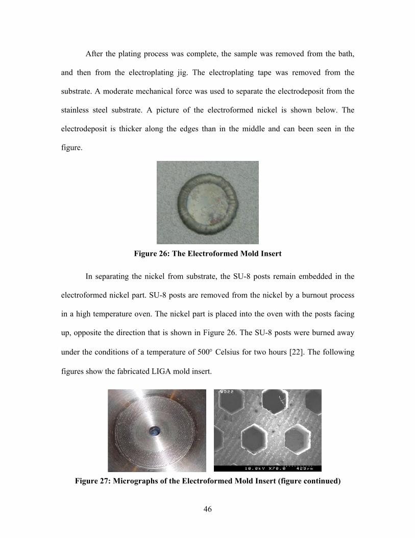
After the plating process was complete, the sample was removed from the bath,
and then from the electroplating jig. The electroplating tape was removed from the
substrate. A moderate mechanical force was used to separate the electrodeposit from the
stainless steel substrate. A picture of the electroformed nickel is shown below. The
electrodeposit is thicker along the edges than in the middle and can been seen in the
figure.
Figure 26: The Electroformed Mold Insert
In separating the nickel from substrate, the SU-8 posts remain embedded in the
electroformed nickel part. SU-8 posts are removed from the nickel by a burnout process
in a high temperature oven. The nickel part is placed into the oven with the posts facing
up, opposite the direction that is shown in Figure 26. The SU-8 posts were burned away
under the conditions of a temperature of 500° Celsius for two hours [22]. The following
figures show the fabricated LIGA mold insert.
Figure 27: Micrographs of the Electroformed Mold Insert (figure continued)
46

47

3. Molding
3. 1 Injection Molding Machine
The molding of plastic components from the electroformed mold insert is the last
stage in the three-step LIGA process. This step forces molten plastic into the recesses of
the mold insert, thus producing features with the same pattern as the features of the SU-8
posts achieved after the exposure process. There are a variety of methods that can be used
to mold microstructures, including injection molding. The injection molding process was
chosen for the molding process with the newly formed tapered mold insert. Injection
molding (as opposed to embossing) was chosen because it allows for the rapid production
of plastic components from the micromold. Decreased ejection forces associated with a
tapered mold insert are expected to improve the process’ ability to rapidly produce parts
by decreasing the total cycle time.
The injection molding machine used for the molding process is a reciprocating
screw machine. The reciprocating screw serves two purposes. First, by rotating, the screw
moves the plastic thru the heating section to an accumulation area. During this transport
the heat produced by the heaters melts the material. The rotating screw also helps in the
melting process by supplying mechanical heat by the shearing action on the viscous
plastic [3]. Figure 28 shows a diagram of a typical reciprocating screw machine.
The cylinder that houses the screw rides on a carriage that moves laterally and
separates the cylinder from the sprue. The cylinder houses four chambers with individual
heaters to maintain the temperature inside of the barrel. The machine also allows for the
screw to move laterally inside of the cylinder. The movement of the screw is the action
48

Figure 28: Diagram of a Typical Injection Molding Machine
that forces the material into the mold cavity and recesses in the insert. In addition, the
mold cavity moves with the same forward and backward motion separating the mold
from the sprue. This allows access to the mold when not molding and provides the
clamping force during injection. The machine is powered through hydraulic pressure
provided by motor located in the rear of the machine.
The reciprocating screw injection molding machine follows a basic sequence of
operations to produce molded parts. Starting with an empty cylinder and the mold open,
the material in the form of pellets falls from the hopper into the rear section of the screw.
The screw rotates forcing the pellets forward. As the pellets move forward, the heaters
and the shearing action of the screw plasticizes the material to a fluid state. The melted
material is then deposited into the barrel between the screw and the sprue. The plasticized
material accumulates in the chamber until it is completely filled with material. When the
screw continues to rotate, the pressure builds up in the barrel, and pushes the screw back
into the cylinder towards the motor. This provides a reservoir of fluid plastic in front of
the screw ready for injection. The mold then closes and the carriage is moved forward
engaging it to the sprue. The screw is then pushed forward with the desired pressure, and
49

injection takes place. The plastic fills the mold cavity and recesses. The pressure is held
until the material freezes in the mold. This pressure is called the holding pressure and
time required to freeze the plastic in the mold the holding time. After the holding time the
screw begins to rotate. This pushes more fluid material into the chamber again forcing the
screw back. The mold cavity is then opened and the part is ejected. The mold closes, and
the machine is ready for another injection.
The sequence of events that is described above constitutes the total cycle of the
machine. The cycle time is a crucial parameter effecting the cost-effectiveness of the
process. As the time decreases the parts are manufactured faster increasing profit.
Figure 29: Injection Molding Sequence Steps in Relation to Cycle Time
The cycle time is dominated by the need to heat and then cool the mold insert.
Before the plastic can be injected, the mold insert must be heated to an appropriate
temperature. If the mold temperature is too low during injection the material will freeze
prematurely causing incomplete filling of the mold and weld lines [7]. In micromolding
this problem is increased due to the high ratio of contact surface to unit volume in the
narrow channels of the microfeatures [7]. During the process, after raising the
temperature to the appropriate value, the mold must then be cooled in order to eject the
50

part. This cooling process freezes the material forming the part. In molding with
conventional micromold inserts, the mold temperature had to be reduced significantly in
order to prevent the part from deforming during ejection. The differences in the required
temperatures both for injection and ejection stages are quite considerable, and the time
necessary to complete this change in temperature is quite significant. However, a LIGA
mold insert with tapered features would still need to be heated to prevent premature
freezing during injection, but the material would need to be cooled to a temperature much
less since the ejection forces associated with extraction would be reduced by the taper.
The time necessary to cool the mold insert for ejection and then reheating it for injection
is reduced, decreasing the cycle time and increasing productivity.
The injection molding machine used in the molding processes was an Arburg
Allrounder 170 CMD reciprocating screw machine. Ejector pins, front and rear mold
platens, and various other accessories were machined to prepare the injection molding
machine for molding. The front mold platen or moving platen slides to and away from the
back plate opening and closing the mold. This plate houses the mold insert and
subsequently the heating and cooling components for the mold. Also, the ejector pins
pass through the plate in order to eject the part from the mold. The mold insert fixture in
the front plate was designed to fit a mold insert mounted on a disk 4.75 inches in
diameter and approximately a quarter inch thick. The moving platen was machined with a
pocket so that the disk slips into the front side of the plate with only the electroformed
features of the insert protruding. The pocket and the disk are machined to high tolerances
to ensure that when the mold closes, the two surfaces remain parallel applying equal
adequate pressure during injection.
51

Ejector pins also reside in the moving plate. Ten ejector pins and four return pins
made of certified H-13 hot work die steel pass through the front plate. Nine ejector pins
are housed in the mold pocket and are used to directly eject the piece from the mold. The
remaining ejector pin forces the frozen sprue and runner from the front platen with the
part. During the molding process, after the holding time is completed, the mold opens
revealing the newly formed part still affixed to the insert. The ejector pins are then forced
forward through the front plate by a hydraulic ram, and the piece is ejected from the
insert. When the part is removed from the machine, the mold begins to close, and the
ejector pins are in the extended position. The four return pins are pressed against the rear
mold platen or fixed platen pushing back the ram and the ten ejector pins to their original
position. The nine ejector pins are 0.1875 inches in diameter, and the remaining ejector
pin is 0.25 inches. The four return pins measure 0.375 inches in diameter. The through
holes were drilled and reamed to tight tolerances to prevent flashing around the diameter
of the pins. The pins were cut to length in order that they also sit flush against the front
face of the platen when fully retracted.
Three 1000 watt cylindrical resistor heaters heat the mold. The heaters are 0.375
inches in diameter, and are inserted into the moving plate from the top. Two heaters rest
directly behind the mold insert and are used to directly heat the insert. One heater is
placed in the plate away from the insert, and is used to heat the rest of the plate. The
heaters are controlled by an Omega temperature controller CN76000 Series and
monitored by a thermocouple inserted 0.125 inches behind the mold insert. The desired
mold temperature is set into the controller and the heaters maintain the temperature.
In order to cool the mold, coolant is pumped through the platen. The plate is
drilled with three through holes from top to bottom. Two five gallon reservoirs are
52

connected to a pump, which pushes water into and through the plate. The water and heat
exits the plate and is dumped back into the reservoir. A cooling diagram of the front plate
is shown in the figure below.
Figure 30: Cooling Diagram of the Front Plate
The rear platen or fixed platen remains stationary during the molding process.
This plate is equipped with sprue, runner, mold cavity, and a vacuum port. The fixed
platen, also machined out of aluminum, is directly connected to the gate from where the
plasticized material enters the mold during injection. A machining process mills out a
hole through the plate. A sprue bushing is pressed into the hole connecting the gate to the
rear platen. Next, the runner and the mold cavity are machined into the front face of the
rear platen. During injection the plasticized material is forced through the gate then
through the sprue into the mold. A runner is needed to transport the material from the
sprue to the mold cavity where the insert is. The runner is cut into the platen in a half
circle approximately 0.125 inches deep. The mold cavity allows for a variety of
53
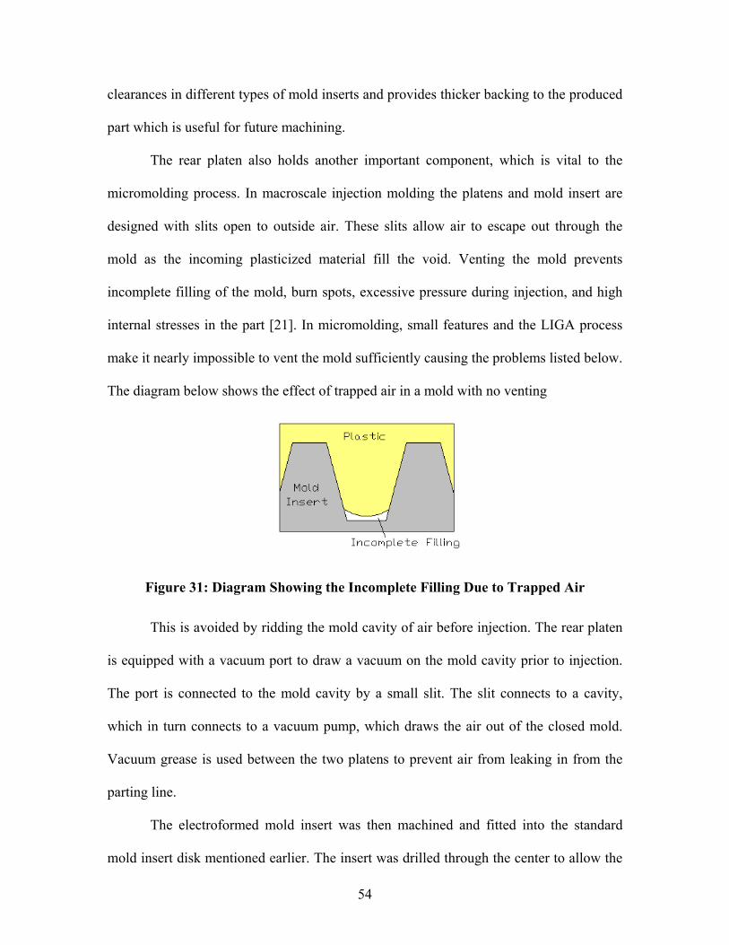
clearances in different types of mold inserts and provides thicker backing to the produced
part which is useful for future machining.
The rear platen also holds another important component, which is vital to the
micromolding process. In macroscale injection molding the platens and mold insert are
designed with slits open to outside air. These slits allow air to escape out through the
mold as the incoming plasticized material fill the void. Venting the mold prevents
incomplete filling of the mold, burn spots, excessive pressure during injection, and high
internal stresses in the part [21]. In micromolding, small features and the LIGA process
make it nearly impossible to vent the mold sufficiently causing the problems listed below.
The diagram below shows the effect of trapped air in a mold with no venting
Figure 31: Diagram Showing the Incomplete Filling Due to Trapped Air
This is avoided by ridding the mold cavity of air before injection. The rear platen
is equipped with a vacuum port to draw a vacuum on the mold cavity prior to injection.
The port is connected to the mold cavity by a small slit. The slit connects to a cavity,
which in turn connects to a vacuum pump, which draws the air out of the closed mold.
Vacuum grease is used between the two platens to prevent air from leaking in from the
parting line.
The electroformed mold insert was then machined and fitted into the standard
mold insert disk mentioned earlier. The insert was drilled through the center to allow the
54

ninth ejector pin to pass through. The following pictures show the platens, the mold
inserts, ejector pins, heating and cooling systems and the vacuum ports.
Figure 32: The Arburg Allrounder 170 CMD Used for Injection Molding
Figure 33: Fixed and Moving Platens in Various Position With Heating/Cooling Systems, Vacuum Ports, and Ejector Pins (figure continued)
55

3. 2 Molding Process
Before the molding process can begin, a material must be chosen. Cyclic Olefin
Copolymer (COC) was selected as the material of choice. COC offers several desirable
qualities in a molding material. It is a glass-clear copolymer made of ethylene and
norbornene, and its most desirable quality is its ease of use in conventional injection
molding. Other desirable qualities include: high moisture barrier and low moisture
absorption, high light transmission, high stiffness and strength, and dimensional stability.
COC is manufactured by Ticona, and is commonly used in packaging for
pharmaceuticals and food, precision optics, medical devices, and laboratory equipment.
The COC comes ready to load into the machine in the form of solid beads. The physical,
mechanical, and thermal properties of COC are listed in Table 4.
A successful injection molding process depends on giving the machine the correct
conditions of pressures, dosages, temperature, and speed of operation. These conditions
vary to a great extent with the machine used, each individual mold, and the material
being molded. Several important parameters are described below. The injection pressure
and the holding pressure are two very important parameters in the molding process. The
56

Table 4: The Properties of Ticona’s Cyclic Olefin Copolymer
Property Value Units Physical Density 1020 kg/m3 Melt Flow Rate 30 gm/10 min Water Absorption < 0.01 %
Mechanical Tensile Modulus 2600 MPa Tensile Stress at Yield 66 MPa Tensile Strain at Yield 10 % Thermal Thermal Expansion 0.8 e-4/deg C Melt Temperature 190-250 deg C
injection pressure is the pressure exerted on the material in the cylinder by the ram or
screw during injection. This pressure is used in conveying the material to the mold and
filling the mold. The holding pressure is the force the screw applies to the material to
essentially pack the mold after during injection. The Arburg machine allows holding
pressures to vary over a first and second stage. The first stage starts at lower pressures
and rises in a series of five steps. The second stage continues increasing the pressure
applied with an additional five steps. The period of time in which the two stages are
completed can be adjusted and are known as the holding times.
The rate at which the machine moves the plasticized material into the mold is
known as the injection rate. The injection rate required is a function of how fast the
material freezes in the mold. The freezing process relates directly to the mold
temperature, nozzle temperature, and the material’s melt temperature as well as the
dimensions of the mold. The injection rate of the material into the mold cavity can be
varied during injection. Five different flow rates can be achieved at different intervals of
57

injection. For instance, 50 cm3/sec of material can be shot until 15 cm3 of material enters
the mold.
When the mold closes and injection occurs, the clamping force keeps the mold
from blowing open from the injection and holding pressures. The screw backpressure is
the amount of pressure required to push the screw backwards while accumulating melt
for injection. The shot capacity or dose is the amount of material, which can be injected
during one cycle of the machine. The approximate dose can be calculated by measuring
the volume of the mold cavity. Five different temperatures are monitored during
injection molding. At three different stages along the barrel of the machine the
temperature inside near the screw is measured. These temperatures are the feedback to
the heaters that plasticize the molding material. A fourth thermocouple monitors the
nozzle of the barrel near the gate where the melt enters the mold. The final thermocouple
is placed directly behind the mold in the moving platen and monitors the mold
temperature.
The process of determining the appropriate molding parameters is based on
empirical observation. A dummy mold is used in a trial-and-error process to finely tune
suggested parameters from the manufacturer of the material and from previous molding
experience. The suggested parameters are loaded into the machine and a trial shot is run.
The piece is examined and appropriate changes are made. This process is repeated until
the parts made with the dummy mold are satisfactory. Table 5 contains the final
parameters used for the successful molding of the parts.
After the parameters are finalized, the dummy mold was then replaced with the
electroformed tapered mold insert. The injection molding process was performed and the
mold opened to reveal the newly formed part. The ejector pins were extended and the part
58

Table 5: Final Molding Parameters for Successful Injection
Injection Stage Flow Rate Volume Stage One 50 cm3/s 15 cm3 Stage Two 40 cm3/s 14 cm3 Stage Three 25 cm3/s 13 cm3 Stage Four 10 cm3/s 10 cm3 Stage Five 5 cm3/s 9 cm3 Pressure Injection Pressure 1300 bar 1st Holding Pressure 2nd Holding Pressure Stage Stage One 150 bar One 300 bar Two 150 bar Two 350 bar Three 200 bar Three 400 bar Four 200 bar Four 450 bar Five 250 bar Five 450 bar Temperature Ejector Pins Barrel One 225 deg C Extend Force 5 kN Barrel Two 235 deg C Retract Force 1 kN Barrel Three 245 deg C Extend Speed 10 mm/s Nozzle 245 deg C Retract Speed 300 mm/s Mold 150 deg C Mold Closing Dosage Closing Force 12 kN Melt Accumulation 31 cm3 Opening Force 12 kN Screw Back Press. 40 bar Clamping Force 150 kN
ejected cleanly. The process was performed repeatedly, and the resulting parts were
evaluated under a microscope. Under the microscope, it was apparent that the parts
produced were not sufficient due to incomplete filling. Although the parts were not
completely filled, there was no evidence that the parts suffered damage from ejection
forces. The following figure shows a part with incomplete filling.
59

Figure 34: Molded Part with Incomplete Filling
The rounded tops indicated that the material was not penetrating fully into the
mold. This problem can be due to several reasons. Injection parameters such as holding
pressure, injection pressure, and flow rate can sometimes be altered to achieve better
results. These parameters were altered several times in a trial and error process to resolve
the problem, and were unsuccessful. Another possible reason for incomplete filling was
that the mold temperature was too low and the material was freezing in the narrow
channels of the posts. Again trial and error runs were completed using varying mold
temperatures well above the suggested parameters given by the material’s manufacturer.
The molding process remained unsuccessful. It was then decided that the mold cavity was
not under sufficient vacuum, and air was being trapped in the mold insert. The vacuum
system was in place, and being used during injection, but air was still entering into the
cavity. The incoming air was due to the area around the nine ejector pins and the moving
60
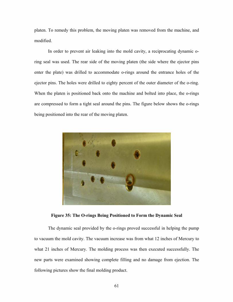
platen. To remedy this problem, the moving platen was removed from the machine, and
modified.
In order to prevent air leaking into the mold cavity, a reciprocating dynamic o-
ring seal was used. The rear side of the moving platen (the side where the ejector pins
enter the plate) was drilled to accommodate o-rings around the entrance holes of the
ejector pins. The holes were drilled to eighty percent of the outer diameter of the o-ring.
When the platen is positioned back onto the machine and bolted into place, the o-rings
are compressed to form a tight seal around the pins. The figure below shows the o-rings
being positioned into the rear of the moving platen.
Figure 35: The O-rings Being Positioned to Form the Dynamic Seal
The dynamic seal provided by the o-rings proved successful in helping the pump
to vacuum the mold cavity. The vacuum increase was from what 12 inches of Mercury to
what 21 inches of Mercury. The molding process was then executed successfully. The
new parts were examined showing complete filling and no damage from ejection. The
following pictures show the final molding product.
61

Figure 36: Final Injection Molded Part
62

4. Conclusions
The ability to manufacture LIGA based mold inserts with draft angles has
important consequences. Before, the team has been unable to mold the COC posts using
an insert with vertical walls that is otherwise identical to the tapered mold insert. The
reduced ejection forces associated with molding tapered structures will open the doors to
molding a wider range of geometries and material combinations which were previously
not possible in injection molding.
Based on the research of tapered LIGA mold inserts presented in this paper, the
following conclusions were drawn:
• Using the modified tilt and rotate exposure technique at CAMD tapered
structures can be produced. The sidewalls of the exposed photoresist have
exceptional directional finish as with normal LIGA exposures.
Dimensions of the exposed structures followed predicted geometries based
on theory. The taper angle of the structures did not affect the
electroplating process, and a successful tapered mold was produced.
• The tapered mold insert was molded successfully by the use of an
injection molding machine. Issues directly related to micromolding (mold
temperature and vacuuming) were addressed and solved. The ejection of
the molded parts was accomplished without structural damage to the posts.
• For cases where extremely tight dimensional control is important, the gap
must be very accurately controlled. An exposure jig can be manufactured
to ensure gap spacing and reduce the tendencies of the graphite x-ray mask
63

to bow. This will prevent the varying dimensions presented previously in
this paper.
• Further investigations need to be done to characterize the reduction of the
ejection forces. A mold insert with vertical sidewalls and similar
dimensions should be fabricated and molded to compare between the two.
Using a pressure transducer the ejection forces can be more closely
monitored and evaluated.
• The effect of tapered mold inserts needs to be investigated with other
processes used by the LSU Microsystems Team. This includes work with
molding procedure involving metals, ceramics, and silicon.
64

Bibliography [1] Bertsch, A., Lorenz, H., and Renaud P., “Combining Microstereolithography and
Thick Resist UV Lithography for 3-D Microfabrication”, Swiss Federal Institute of Technology.
[2] Bogdanov, A. L., and Peredkov S. S., “Use of SU-8 Photoresist for Very High
Aspect Ratio X-ray Lithography”, MAX-Lab, University of Lund. [3] Bown, J., “Injection Molding of Plastic Components”, McGraw-Hill Book
Company, London, 1979. [4] Cedorge, T. and Colton, J., “Draft Angle and Surface Roughness Effects on
Stereolithography Molds”, Polymer Engineeringand Science, July 2000, Vol. 40, No. 7, pp 1581- 1588.
[5] Core Plastique, “Adequate Draft Angles and Structural Forms ”,
http://www.core77.com /resource/plastique/structural.html [6] Cremers, C., Bouamrane, F., Singleton, L., Schenk, R., “SU-8 as Resist Material
for Deep X-ray Lithography”, Microsystem Technolgies, 7, 2001, pp 11-16. [7] Despa, M.S., Kelly K.W., and Collier, J.R., “Injection Molding of Polymeric
LIGA HARMs”, Microsystem Technologies, 6, 1999, pp 60-66. [8] Dym, J., “Injection Molds and Molding”, 2nd Edition, Kluwer Academic
Publishers, Boston, 1987. [9] Glanvill, A. B., “Plastics Engineer’s Data Book”, 1st Edition, Industrial Press
Incorporated, New York, 1973. [10] Glanville, A. and Denton, E., “Injection Mould Design Fundamentals”, Industrial
Press, New York, 1965. [11] Harris, R., Hopkinson, N., Newlyn, H., Hague, R., and Dickens, P., “Layer
Thickness and Draft Angle Selection for Stereolithography Injection Mould Tooling”, International Journal of Production Research, 2002, Vol. 40, No. 3, pp 719-729.
[12] IDSA M&P Resource Online, “A Few Words About Draft”, http://www.idsa-
mp.org/proc/plastic/injection/injection_design_4.htm [13] Judy, J. and Motta P., “MEMS Nickel Electroplating”, University of California
Los Angeles, 2000.
65
[14] Lee, J. L., Madou, M. J., Koelling, K. W., Daunert, S., Lai, S., Koh, C.G., Juang,
Y., Lu, Y., and Yu, Liyong Y., “Design and Fabrication of CD-Like Microfluidic Platforms for Diagnostics: Polymer-Based Microfabrication”, Biomedical Microdevices, 3:4, Kluwer Academic Publishers, 2001, pp. 339-351.
[15] Madou, M., “Fundamentals of Microfabrication”, CRC Press, Boca Raton, 1997. [16] Marques, C., “Heat Transfer of a Microstructure-Covered Cylinder in Crossflow”,
M.S. Thesis, Louisiana State University, Baton Rouge, August 1997. [17] Microchem Corporation, “NANO SU-8 Negative Tone Photoresists Formulations
25-75, www.microchem.com , 2001. [18] Pham, G.T. and Colton, J., “Ejection Force Modeling for Stereolithography
Injection Molding Tools”, Polymer Engineering and Science, April 2002, Vol. 42, No. 4, pp 681-693.
[19] Prentice, G., “Electrochemical Engineering Principles”, Prentice Hall, New Jersy,
1991. [20] Rees, H., “Understanding Injection Mold Design”, Hanser Gardner Publications,
Cincinnati, 2001. [21] Rosato Donald, Rosato Dominick, “Injection Molding Handbook”, 2nd Edition,
Chapman & Hall, New York, 1995. [22] Zhang, J., “LIGA Mold Insert Fabrication Using SU-8 Photoresist”, M.S. Thesis,
Louisiana State University, Baton Rouge, December 2002.
66

Vita
Ryan Anthony Turner was born in Bellflower, California, on May 7, 1978. He is
the son of Richard and Peggy Turner, and the older brother of two sisters: Amy and
Mary. Ryan Turner was raised in Houma, Louisiana, a small bayou town sixty miles
southwest of New Orleans. In May of 1996, he graduated from Terrebonne High School
and proceeded to attend Louisiana State University where he graduated with a Bachelor
of Science degree in Mechanical Engineering in May of 2001. He received his Master of
Science degree in Mechanical Engineering from Louisiana State University in December
of 2002.
67