technical information oundationtm fieldbus
TRANSCRIPT

TechnicalInformation
DAQSTATIONApplications of FOUNDATIONTM FIELDBUS
TI 04L01A01-14E
TI 04L01A01-14E©Copyright July 20011st Edition July 2001

Blank Page

All Rights Reserved. Copyright © 2001, Yokogawa Electric Corporation TI 04L01A01-14E
i<Toc> <Introduction>
June 5,2001-00
IntroductionThis document explains detailed specifications of the optional FOUNDATIONTM Fieldbus capabilitiesfor the DAQSTATION. Read this manual thoroughly to make the most of the functions of theDX100/DX200.

Blank Page

All Rights Reserved. Copyright © 2001, Yokogawa Electric Corporation TI 04L01A01-14E
Toc-1<Int>
June 5,2001-00
CONTENTSIntroduction........................................................................................................... i
1. Overview of Function ............................................................................. 1-11.1 Overview of the DX/MV ................................................................................... 1-1
1.2 Basic Function ................................................................................................ 1-3
1.3 Link Master Function .................................................................................... 1-13
2. Connecting to the Fieldbus .................................................................... 2-12.1 Fieldbus Communication Interface Specifications ....................................... 2-1
2.2 Connecting to the Terminal ............................................................................ 2-2
3. Setting the Fieldbus Functions .............................................................. 3-13.1 Overview of the Procedure in Setting the Parameters .................................. 3-1
3.2 Setting the Node Address, PD Tag, and Block Tag ........................................ 3-4
3.3 Setting Example .............................................................................................. 3-5
3.4 Changing the Block Mode .............................................................................. 3-8
3.5 Setting the Function That Outputs the Measured Data(AI Function Block) ....................................................................................... 3-10
3.6 Setting the Function That Outputs the Measured Data(MAI Function Block) .................................................................................... 3-15
3.7 Setting the Function That Receives Measured Data(MAO Function Block) ................................................................................... 3-16
3.8 Setting the Trend Function (Trend Object) ................................................... 3-20
3.9 Setting the Function That Transmits Alerts ................................................. 3-21
3.10 Prohibiting Writing to Parameters ................................................................ 3-25
3.11 Setting the Communications between Function Blocks (Link Object and Virtual Communication Relationship) ............................. 3-26
3.12 Setting the Schedule of Function Blocks .................................................... 3-29
3.13 Specifying Link Master Device or Basic Device .......................................... 3-30
3.14 Setting the Node Address Range to Be Used (Link Master Function) ................................................................................ 3-31
3.15 Setting the Operating Conditions of Communications (Link Master Function) ................................................................................ 3-32
TI 04L01A01-14E 1st Edition
Applications of FOUNDATIONTM Fieldbus Functionality ofDAQSTATION

Toc-2
All Rights Reserved. Copyright © 2001, Yokogawa Electric Corporation
<Int>
TI 04L01A01-14E June 5,2001-00
4. Operation ................................................................................................ 4-14.1 Starting the Operation and Operations on the Host
and the DX/MV ................................................................................................. 4-1
4.2 Handling Alerts ............................................................................................... 4-2
4.3 Using the Using the Simulation Function (AI Function Block) ..................... 4-5
4.4 Checking the Status of the Communication Input Data ................................ 4-7
5. Troubleshooting ..................................................................................... 5-15.1 Handling the I/O Status ................................................................................... 5-1
5.2 Handling .......................................................................................................... 5-9
5.3 Handling the Device Status (DEVICE_STATUS) .......................................... 5-13
5.4 Troubleshooting the ...................................................................................... 5-15
Appendix 1 Terminology .........................................................................App.-1
Appendix 2 Parameters ...........................................................................App.-5

All Rights Reserved. Copyright © 2001, Yokogawa Electric Corporation TI 04L02A01-14E
1-1<Toc> <1. Overview of Function>
June 5, 2001-00
1. Overview of Function
1.1 Overview of the DX/MV
■ Fieldbus Standard
The DX/MV can connect to FOUNDATION Fieldbus H1 (transmission speed of 31.25 kb/ s) asdefined by Fieldbus Foundation.
■ Device Type
Link Master Device and Basic Device
The DX/MV is a link master device. It has the function as a scheduler.
The DX/MV can also operate as a Basic Device without using this the link master function.
Host
Fieldbus
Basic DeviceLink Master Device
DX MV
Bus Powered Device
The fieldbus function of the DX/MV is driven by the bus power (the DX/MV itself requires its ownpower supply. The hardware section that controls the fieldbus functions of the DX/MV is driven bythe bus power).
■ Node Address and PD Tag (Physical Device Tag)
All devices on the fieldbus (except power supplies and terminators) are required to have a uniquenode address and PD tag. The address is used to specify the device during communications.The PD tag acts as a tag for field devices. The initial values for the node address and PD tag areas follows.
• Node address: 245
• PD tag: DAQSTATION

1-2
All Rights Reserved. Copyright © 2001, Yokogawa Electric Corporation
<Toc>
TI 04L02A01-14E
<1. Overview of Function>
June 5, 2001-00
■ IDs
The DX/MV has the following ID numbers. These values can be confirmed with the parametervalues in the resource block * .
* For details on the resource block, see section 1.2.
IDs
ID Parameter *1 Value (Hexadecimal) Description
Manufacturer ID MANUFAC_ID 594543 A fixed ID for YOKOGAWA.
Device type DEV_TYPE 1801 A fixed ID indicating the DX/MV.
Device revision DEV_REV xx Device revision number.Revision number The value changes when a
function is modified.
Device description *2 DD_REV xx Device description revisionRevision number number. The value changes when
the device description is modified.*1 : Parameters in the resource block.*2 : For details on the device description, see section 3.1.

All Rights Reserved. Copyright © 2001, Yokogawa Electric Corporation TI 04L02A01-14E
1-3<Toc> <1. Overview of Function>
June 5, 2001-00
1.2 Basic Function■ Structure of Functions
The DX/MV functions are shown in the figure.
AI_MAP
AI_MAP
AI_MAP
AI_MAP
AI_MAP
AI_MAP
AI_MAP
AI_MAP
System/Network Management
Fieldbus function
Fieldbus
Group of parameters
Input/output value
Alert
AI functionblock
Link object
MAO function block
Communication input data
Computation equation (see chapter 11, the DX/MV User's Manual)
MAI functionblock
Transducerblock
Resource block
Measuredvalue
Measurementchannel
DisplayData storage
Computationchannel
PD tagNode addressFunction block execution control
Hardware/software resource controlManufacturer's ID, Device type, Device revision
Communication controlVCR control
AbbreviationProc.:Data processingLink: Link ObjectAlert: Alert ObjectTrend: Trend ObjectView: View ObjectVCR: Virtual Communica- tion Relationship
IN-1
IN-2
IN-3
IN-4
IN-5
IN-6
IN-7
IN-8
OUT-1
OUT
OUT
OUT
OUT
OUT
OUT
OUTProc.
OUT-2
OUT-3
OUT-4
OUT-5
OUT-6
OUT-7
OUT-8
MAO_MAP
MAO_MAP
MAO_MAP
MAO_MAP
MAO_MAP
MAO_MAP
MAO_MAP
MAO_MAP
MAI_MAP
MAI_MAP
MAI_MAP
MAI_MAP
MAI_MAP
MAI_MAP
MAI_MAP
MAI_MAP
Proc.
Proc.
OUT
Link
Link
Link
Link
Link
Link
Link
Link
Trend
Trend:
View
View:
Alert
Alert
Alert
Link
Link
Link
Link
Link
Link
Link
Link
Link
Link
Link
Link
Link
Link
Link
Link
VCR
VCR
VCR
VCR
VCR
VCR
VCR
VCR
VCR
VCR
CH01:
CH30
VCR
VCR
VCR
VCR
VCR
VCR
VCR
VCR
VCR
VCR
VCR
VCR
VCR
VCR
VCRProc.
Proc.
Proc.
Proc.
Proc.
Link :
VCR:
Link VCR
VCR:
VCR
Link VCR
Link VCR
Link VCR
CH31:
CH60
C01:
C30
(system use)

1-4
All Rights Reserved. Copyright © 2001, Yokogawa Electric Corporation
<Toc>
TI 04L02A01-14E
<1. Overview of Function>
June 5, 2001-00
■ Resource Block (RB)
Resource block stores the information of hardware and software resources of the DX/ MV.It stores the device information such as Manufacturer’s ID, Device Type. Only one resource blockexists on each device.For the resource block parameters, see sections 3.7, 3.9, and appendix 2.
■ Transducer Block (TB)
Transducer block connects the measured, computed, and communication input data on the DX/MV to the function block. It processes measured or computed data so that the AI or MAI canhandle, and the data from the MAO so that the computation channel of the DX/MV can handle.For the parameters of the transducer block, see sections 3.5, 3.6, 3.7, and appendix 2.
■ AI (Analog Input) Function Block
Retrieves the measured and computed data (CH01 to CH60, the number of channels differsdepending on models) of the DX/MV to the block and outputs the data to the fieldbus (“OUT” inthe figure). At this point, the following processing can be carried out on the measured andcomputed data (“Proc.” in the figure).
• Scaling (scale to value in an appropriate engineering unit)
• Set alarms
• Square root computation
• Filtering
• Low cut filtering (output 0 for values less than or equal to the specified value)
In addition, there is a simulation function that outputs specified values to the fieldbus as measuredand computed values (see section 4.3).The DX/MV has 8 AI function blocks. The transducer block parameter (“AI_MAP” in the figure) isused to specify the measurement or computation channel data that is to be retrieved to the AIfunction block. An AI function block can handle a measured or computed datum.For the AI function block parameters, see section 3.5 and appendix 2.
■ MAI (Multiple Analog Input) Function Block
Retrieves the measured and computed data (CH01 to CH60, the number of channels differsdepending on models) of the DX/MV to the block and outputs the data to the fieldbus (“OUT-1” to“OUT-8” in the figure). Up to 8 data sets can be handled simultaneously. The MAI does not havethe computation functions as with the AI, but it allows transmission of large amounts of data usinga small number of setup parameters with a short execution time.The DX/MV has one MAI function block. The transducer block parameter (“MAI_MAP” in thefigure) is used to specify the measurement or computation channel data of the DX/ MV that is tobe retrieved to the MAI function block.For the MAI function block parameters, see section 3.5 and appendix 2.
■ MAO (Multiple Analog Output) Function Block
Retrieves the data from the fieldbus (“IN-1” to “IN-8” in the figure) so that the DX/MV can use thedata as communication input data (CH01 to CH30, the number of communication input datadiffers depending on models). Up to 8 data sets can be handled simultaneously.The DX/MV has one MAO function block. The transducer block parameter is used to assign thedata sets of MAO function block to the communication input data of the DX/ MV. Computationchannels are used to display communication input data on DX/MV.For the MAO function block parameters, see section 3.5 and appendix 2.

All Rights Reserved. Copyright © 2001, Yokogawa Electric Corporation TI 04L02A01-14E
1-5<Toc> <1. Overview of Function>
June 5, 2001-00
■ System/Network Management Function
The DX/MV has the following system/network management functions.
System/Network Management Function
Function Description
Address management Sets the node address and PD tag of the DX/MV.
Time synchronization Synchronizes the time using the time broadcast from the scheduler.
Tag search Searches for a specified tag.
Schedule management Executes the function block according to the schedule.
Communication control Controls communications initiated by the DX/MV.
For the parameters of the system/network management functions, see sections 3.11 to 3.15, andappendix 2.
Virtual Communication Relationship (VCR)
The virtual communication relationship determines the communication method between devices.Once it is configured, communication with other devices can be carried out simply by specifyingthe virtual communication relationship number. The DX/MV has 31 virtual communicationrelationships. One of them is for system use and cannot be altered.For the virtual communication relationship parameters, see section 3.11.
■ Link Object
Link object is a function used by the function block to perform communication. There are 26 linkobjects provided on the DX/MV assuming the following application. The link objects are used byspecifying the parameter for each application.
Assumed Use of Link Objects
Application Number of the link object (assumed)
For trends 1
For alerts 1
For the output (OUT) of the AI function block 1 to 8 8
For MAI function block OUT_1 to OUT_8 8
For MAO function block IN_1 to IN_8 8
For the link object parameters, see section 3.11.

1-6
All Rights Reserved. Copyright © 2001, Yokogawa Electric Corporation
<Toc>
TI 04L02A01-14E
<1. Overview of Function>
June 5, 2001-00
■ Alert Object
Transmits *1 an alert when a specified process alarm occurs or is released in the AI function block,when a block alarm (block error) occurs or is released, when the prohibition of writing to staticparameters *2 is set or released, or when an update event (when a static parameter *2 isoverwritten) occurs. The alert shown in the table below can be transmitted for each block.
*1 : Communication starts when a link object and a virtual communication relationship are specified.*2 : For the attributes of parameters, see appendix 2.
Cause of an Alert
Block Process Alarm Block Alarm, Update EventWrite Lock Alarm
RB Block alarm, Update eventWrite prohibition alarm
TB Block alarm Update event
AI-1, AI-2, HI_HI alarm x 8 Block alarm x 8 Update event x 8AI-3, AI-4, HI alarm x 8AI-5, AI-6, LO alarm x 8AI-7, AI-8 LO_LO alarm x 8
MAI Block alarm Update event
MAO Block alarm Update event
Number of 32 13 12causes (total)
Number of 1 1 1alert objects
The DX/MV has three alert objects. When multiple alarms occur, alert is transmitted by usingthese alert objects. However, if there is no free alert object, the transmission is put on wait.For the alert object parameters, see appendix 2. For the parameters related to alert transmission,see section 3.9.
■ Trend Object
The trend object samples and holds the values of a specified input/output parameter, andperiodically transmits* the values in groups (16 samples).
* Communication starts when a trend object, link object, and a virtual communication relationship are specified.
There are eight trend objects in the DX/MV. The trend of the parameters in the table below can betransmitted.
Trend Target Parameters
Function Block Target parameter
Eight AIs FIELD_VAL, PV, OUT
MAI OUT_1, OUT_2, OUT_3, OUT_4, OUT_5, OUT_6, OUT_7, OUT_8
MAO IN_1, IN_2, IN_3, IN_4, IN_5, IN_6, IN_7, IN_8
Total 40
The execution time (see p.1-11) that is specified for the FB of the DX/MV is a value that is derivedwith the premise that up to one trend object is to be used. If multiple trend objects are used on asingle function block, the execution time may exceed the specified value (30 ms) and causeproblems in which the function block is not executed according to the schedule.For the trend object parameters, see appendix 2. For the parameter settings, see section 3.8.

All Rights Reserved. Copyright © 2001, Yokogawa Electric Corporation TI 04L02A01-14E
1-7<Toc> <1. Overview of Function>
June 5, 2001-00
■ View Object
View object is used when reading several parameters of a function block at once. By collectivelyretrieving the parameters,* the load of the communication process is reduced.There are four types of view objects.
* The grouping of the parameters in VIEW_1 to VIEW_4 is fixed for each block and cannot be changed.
View Object Types
No. Symbol Description
1 VIEW_1 A set of dynamic parameters * required by the operator for operation (OUT, PV, IN,MODE, etc).
2 VIEW_2 A set of static parameters * that need to be indicated to the operator (scalingparameter, etc).
3 VIEW_3 A set of all dynamic parameters. *
4 VIEW_4 A set of static parameters * not included in VIEW_2.* For the parameter attributes, see appendix 2.
All the blocks of the DX/MV have one of each type VIEW_1 to VIEW_4. Each view object canread them using the following index numbers.*
* For the index numbers, see “Parameters” in this section.
Index Number of the View Object
Function Block VIEW_1 VIEW_2 VIEW_3 VIEW_4
RB 40100 40101 40102 40103
TB 40200 40201 40202 40203
AI-1 40400 40401 40402 40403
AI-2 40410 40411 40412 40413
AI-3 40420 40421 40422 40423
AI-4 40430 40431 40432 40433
AI-5 40440 40441 40442 40443
AI-6 40450 40451 40452 40453
AI-7 40460 40461 40462 40463
AI-8 40470 40471 40472 40473
MAI 40900 40901 40902 40903
MAO 41000 41001 41002 41003
The parameters of VIEW_1 through VIEW_4 that are specified for each function block are storedin order in the view object.For example, the view object corresponding to VIEW_2 of the transducer block (index number40201) has the following construction.
Construction of the View Object Corresponding to VIEW_2 of the TB
Index No. Parameter
40201 ST_REVTRANSDUCER_TYPE
The parameters that are stored in VIEW_1 through VIEW_4 of each block are shown below.The value in the VIEW column represents the parameter size (in bytes). “R” denotes the relativeindex No. (see p.1-10).

1-8
All Rights Reserved. Copyright © 2001, Yokogawa Electric Corporation
<Toc>
TI 04L02A01-14E
<1. Overview of Function>
Parameters in the View Object of the Resource Block
R Parameter VIEW_1 VIEW_2 VIEW_3 VIEW_4
1 ST_REV 2 2 2 2
2 TAG_DESC
3 STRATEGY 2
4 ALERT_KEY 1
5 MODE_BLK 4 4
6 BLOCK_ERR 2 2
7 RS_STATE 1 1
8 TEST_RW
9 DD_RESOURCE
10 MANUFAC_ID 4
11 DEV_TYPE 2
12 DEV_REV 1
13 DD_REV 1
14 GRANT_DENY 2
15 HARD_TYPES 2
16 RESTART
17 FEATURES 2
18 FEATURE_SEL 2
19 CYCLE_TYPE 2
20 CYCLE_SEL 2
21 MIN_CYCLE_T 4
22 MEMORY_SIZE 2
23 NV_CYCLE_T 4
24 FREE_SPACE 4
25 FREE_TIME 4 4
26 SHED_RCAS 4
27 SHED_ROUT 4
28 FAULT_STATE 1 1
29 SET_FSTATE
30 CLR_FSTATE
31 MAX_NOTIFY 1
32 LIM_NOTIFY 1
33 CONFIRM_TIME 4
34 WRITE_LOCK 1
35 UPDATE_EVT
36 BLOCK_ALM
37 ALARM_SUM 8 8
38 ACK_OPTION 2
39 WRITE_PRI 1
40 WRITE_ALM
41 ITK_VER 2
42 SOFT_REV
43 SOFT_DESC
44 SIM_ENABLE_MSG
45 DEVICE_STATUS_1 4
46 DEVICE_STATUS_2 4
47 DEVICE_STATUS_3 4
48 DEVICE_STATUS_4 4
49 DEVICE_STATUS_5 4
50 DEVICE_STATUS_6 4
51 DEVICE_STATUS_7 4
52 DEVICE_STATUS_8 4
Total 22 30 54 31
Parameters in the View Object of the Transducer Block
R Parameter VIEW_1 VIEW_2 VIEW_3 VIEW_4
1 ST_REV 2 2 2 2
2 TAG_DESC
3 STRATEGY 2
4 ALERT_KEY 1
5 MODE_BLK 4 4
6 BLOCK_ERR 2 2
7 UPDATE_EVT
8 BLOCK_ALM
9 TRANSDUCER_DIRECTORY
10 TRANSDUCER_TYPE 2 2 2 2
11 XD_ERROR 1 1
12 COLLECTION_DIRECTORY
13 AI_MAP 16
14 MAI_MAP 16
15 MAO_MAP 16
16 ALARM_SUM 8 8
17 DEV_ID
18 DEV_KEY
19 EEPROM_STATE
20 UART_STATISTICS
21 STACK_STATISTICS_1
22 STACK_STATISTICS_2
23 STACK_CONF
24 EXEC_FB_CNT
Total 19 4 19 55
Parameters in the View Object of the AI Function Block
R Parameter VIEW_1 VIEW_2 VIEW_3 VIEW_4
1 ST_REV 2 2 2 2
2 TAG_DESC
3 STRATEGY 2
4 ALERT_KEY 1
5 MODE_BLK 4 4
6 BLOCK_ERR 2 2
7 PV 5 5
8 OUT 5 5
9 SIMULATE
10 XD_SCALE 11
11 OUT_SCALE 11
12 GRANT_DENY 2
13 IO_OPTS 2
14 STATUS_OPTS 2
15 CHANNEL 2
16 L_TYPE 1
17 LOW_CUT 4
18 PV_FTIME 4
19 FIELD_VAL 5 5
20 UPDATE_EVT
21 BLOCK_ALM
22 ALARM_SUM 8 8
23 ACK_OPTION 2
24 ALARM_HYS 4
June 5, 2001-00

All Rights Reserved. Copyright © 2001, Yokogawa Electric Corporation TI 04L02A01-14E
1-9<Toc> <1. Overview of Function>
R Parameter VIEW_1 VIEW_2 VIEW_3 VIEW_425 HI_HI_PRI 1
26 HI_HI_LIM 4
27 HI_PRI 1
28 HI_LIM 4
29 LOW_PRI 1
30 LOW_LIM 4
31 LOW_LOW_PRI 1
32 LOW_LOW_LIM 4
33 HI_HI_ALM
34 HI_ALM
35 LOW_ALM
36 LOW_LOW_ALM
Total 31 26 31 46
Parameters in the View Object of the MAI Function Block
R Parameter VIEW_1 VIEW_2 VIEW_3 VIEW_4
1 ST_REV 2 2 2 2
2 TAG_DESC
3 STRATEGY 2
4 ALERT_KEY 1
5 MODE_BLK 4 4
6 BLOCK_ERR 2 2
7 CHANNEL 2
8 OUT_1 5 5
9 OUT_2 5 5
10 OUT_3 5 5
11 OUT_4 5 5
12 OUT_5 5 5
13 OUT_6 5 5
14 OUT_7 5 5
15 OUT_8 5 5
16 UPDATE_EVT
17 BLOCK_ALM
Total 48 2 48 7
Parameters in the View Object of the MAO Function Block
R Parameter VIEW_1 VIEW_2 VIEW_3 VIEW_4
1 ST_REV 2 2 2 2
2 TAG_DESC
3 STRATEGY 2
4 ALERT_KEY 1
5 MODE_BLK 4 4
6 BLOCK_ERR 2 2
7 CHANNEL 2
8 IN_1 5 5
9 IN_2 5 5
10 IN_3 5 5
11 IN_4 5 5
12 IN_5 5 5
13 IN_6 5 5
14 IN_7 5 5
15 IN_8 5 5
16 MO_OPTS 2
17 FSTATE_TIME 4
18 FSTATE_VAL1 4
19 FSTATE_VAL2 4
20 FSTATE_VAL3 4
21 FSTATE_VAL4 4
22 FSTATE_VAL5 4
23 FSTATE_VAL6 4
24 FSTATE_VAL7 4
25 FSTATE_VAL8 4
26 FSTATE_STATUS 1 1
27 UPDATE_EVT
28 BLOCK_ALM
Total 49 2 49 45
June 5, 2001-00

1-10
All Rights Reserved. Copyright © 2001, Yokogawa Electric Corporation
<Toc>
TI 04L02A01-14E
<1. Overview of Function>
■ Parameters
The fieldbus function of the DX/MV is configured by setting parameters that belong to the VirtualField Devices (see appendix 1). Parameters for the system/network management function are inthe Management Information Base Virtual Field Device (MIB-VFD), and parameters for functionblocks are in the Function Block Virtual Field Device (FB-VFD).
Index No.0:
1000:
2000:
4000:
4100:
4200:
4300:
4400:
4500:
4600:
4700:
9000:
10000:
30000:
31000:
32000:
40000:
FunctionCommon items
Resource block
Transducer block
AI function block-1
AI function block-2
AI function block-3
AI function block-4
AI function block-5
AI function block-6
AI function block-7
AI function block-8
MAI function block
MAO function block
Link object
Alert object
Trend Object
View object
Index No.0:
258:
290:
FunctionCommon items
System management
Network management
Management Information Base Virtual Field Device (MIB-VFD)
Function Block Virtual Field Device(FB-VFD)
June 5, 2001-00

All Rights Reserved. Copyright © 2001, Yokogawa Electric Corporation TI 04L02A01-14E
1-11<Toc> <1. Overview of Function>
Index No., Sub Index No., Relative Index No.
The DX/MV assigns the index numbers to the parameters. If the parameter consists of a set ofsub parameters, sub parameters have sub index numbers. In addition, the parameters of theresource block, transducer block, AI function blocks, MAI function block, and MAO function blockhave a relative index number that are assigned the values 0, 1, 2, and so on from the head of theblock.For example, the parameters of the resource block are stored in the area corresponding to indexnumbers 1000 to 1052. The parameters are assigned relative index numbers from 0 to 52.The parameter “MODE_BLK” at the relative index number 5 has sub parameters with subindexnumbers 1 to 4.
Parameters of the Resource Block
Index No. Relative Index No. Parameter
1000 0 Block
1001 1 ST_REV
1002 2 TAG_DESC
1003 3 STRATEGY
1004 4 ALERT_KEY
1005 5 MODE_BLK
Sub Index No. Sub parameter
1 Target
2 Actual
3 Permitted
4 Normal
1006 6 BLOCK_ERR
: : :
1051 51 DEVICE_STATUS_7
1052 52 DEVICE_STATUS_8
A parameter is identified using the index number, sub index number and the relative indexnumber.For the parameters of the DX/MV, see appendix 2.
June 5, 2001-00

1-12
All Rights Reserved. Copyright © 2001, Yokogawa Electric Corporation
<Toc>
TI 04L02A01-14E
<1. Overview of Function>
■ Execution of the Function Block
Execution Time
Execution time refers to the time that is required to execute the process of the function block.The table below shows the execution times that are set before shipping. The time cannot bechanged.The execution time is set to a value with a slight margin. However, if there is too much informationto be processed, the process may not be completed within the execution time. In such case,lighten the processing load of the block.
Period of Execution
The period of execution is the time duration at which the process of each block is repeated.Modify the period of execution as necessary. However, since the I/O data is updated at the periodof execution of the transducer block (250 ms), specifying a shorter period may result in the samevalue to be retrieved at consecutive periods.
Block Execution Time and Period of Execution
Block Execution Time Period of Execution
Resource block Self-run Self-run (500 ms)
Transducer block Self-run Self-run (250 ms)
AI function block 30 ms Determined by the schedule.
MAI function block 30 ms Determined by the schedule.
MAO function block 30 ms Determined by the schedule.
Schedule
Since the DX/MV can only process the function blocks sequentially, the function block 2 may notbe executed, as it is scheduled to run in parallel with the function block 1.
Scheduling is not required for the resource and transducer blocks, since they are self-run.
Schedule That Cannot Be Executed
Scheduled to execute the function block 1 and 2 in parallel.
Execution of the function block 1
Execution of the function block 2 (May not be executed)
■ Communication with Other Field Device
To transmit data to or receive data from other devices on the fieldbus, the link objects and thevirtual field devices (VCR) are used.
June 5, 2001-00

All Rights Reserved. Copyright © 2001, Yokogawa Electric Corporation TI 04L02A01-14E
1-13<Toc> <1. Overview of Function>
1.3 Link Master FunctionLink Master Functions
The following scheduler functions are supported.
Link Master Functions
Function *1 Description
Detection of New Devices on the Periodically checks the devices on the fieldbus for newFieldbus devices.
Control of Unscheduled Provides permissions to all devices on the fieldbus inCommunications sequence and periodically when unscheduled
communication is possible.
Control of Scheduled Communications Instructs publishing/subscribing of measured data tofield devices according to the schedule.
Time Synchronization Periodically broadcasts time information. This allows alldevices to have the same time information.
Live List Equalization Broadcasts the live list (LL) *2 to all the link masterdevices on the fieldbus. This allows all the link masterdevices to have the same live list.
Assignment of the Scheduler Rights Assigns the scheduler rights to other link masterdevices.
*1 : The DX/MV does not support the transmission of RR (Round Trip Delay Reply) and Long Address.*2 : Live list is a list of devices that are detected on the fieldbus.
Transition to Scheduler
If the DX/MV determines that there is no scheduler on the fieldbus such as when starting up afieldbus or a preexisting scheduler malfunctions, it declares that it will become a scheduler andmakes the transition. For the transition condition to the scheduler, see appendix 1, “Terminology.”
June 5, 2001-00

Blank Page

All Rights Reserved. Copyright © 2001, Yokogawa Electric Corporation TI 04L01A01-14E
2-1<Toc> <2. Connecting to the Fieldbus>
June 5, 2001-00
2. Connecting to the Fieldbus
2.1 Fieldbus Communication Interface SpecificationsThe fieldbus communication interface specifications of the DX/MV are indicated below.
Fieldbus Communication Interface Specifications
Item Description
Terminal type M4 screws
Output signal Digital signal based on the FOUNDATION Fieldbus H1
Physical layer 113 (standard-power signaling, bus powered, non I.S.)
Number of connected devices *1 Up to 32 (Including the DX/MV)
Connection Multidrop
Intrinsic safety Not applicable
Transmission mode Transmission mode based on the FOUNDATION Fieldbus H1
Transmission speed 31.25 kbps
Communication line condition Power supplied by the communication lineSupply voltage: 9 to 32 VDCSupply current: 16.5 mA (maximum)
Isolation Dielectric strength (between communication terminals and theground terminal): 500 Vrms (50/60 Hz, 1 min.)
Transmission distance *2 Cable type Maximum cable length (reference value)
Type A (twisted pair, shielded per pair) 1900 m#18AWG (0.82 mm 2 )Type A (twisted pair, shielded collectively) 1200 m#22AWG (0.32 mm 2 )
*1 : “32” means the theoretical number of connectable devices. The actual number of connectable devices variesdepending on the installation conditions.
*2 : The transmission distance is limited by the cable type, the power supply to the bus, etc.

2-2
All Rights Reserved. Copyright © 2001, Yokogawa Electric Corporation
<Toc>
TI 04L01A01-14E
<2. Connecting to the Fieldbus>
June 5, 2001-00
2.2 Connecting to the Terminal
■ Terminal Arrangement
Terminals Names
(Rear Panel) FG NC NC + −
SimEnable
Terminal Description
Terminal Description
FG (Frame Ground) Case ground of the DX/MV.
SimEnable Connect to FG when using the simulation function. For information on how touse this terminal, see section 4.3.
NC (No Connection) Not used.
+ Connect to the cable on the positive side of the fieldbus power supply.This terminal is isolated from the ground terminal (including FG terminal).
– Connect to the cable on the negative side of the fieldbus power supply.This terminal is isolated from the ground terminal (including FG terminal).
■ Connection Procedure
WARNING
To prevent the possibility of electric shock, connect the cables with the power turned OFF.
How to Connect the Cable
As shown in the following figure, attach a crimp-on lug with isolation sleeves for 4 mm screws tothe end of the cable. Keep the exposed section from the end of the shield within 5 cm.
Connection
FG + −
Shield Potential Shielded
SimEnable terminal (For information on how to use this terminal, see section 4.3.)

All Rights Reserved. Copyright © 2001, Yokogawa Electric Corporation TI 04L01A01-14E
2-3<Toc> <2. Connecting to the Fieldbus>
June 5, 2001-00
Attaching the Clamp Filter
Attach the clamp filter that came with the package to the cable. Attach it near the DX/MV’sterminal.
Clamp Filter
Fieldbus cable Clamp filter

Blank Page

All Rights Reserved. Copyright © 2001, Yokogawa Electric Corporation TI 04L01A01-14E
3-1<Toc> <3. Setting the Fieldbus Functions>
3. Setting the Fieldbus Functions
3.1 Overview of the Procedure in Setting the Parameters
■ Scope of This Chapter
This chapter describes the settings of the main parameters using the expression when theDevice Description of the DX/MX (see below) is used. For parameters that are not described inthis chapter, see appendix 2.The procedure in setting the parameters varies depending on the configurator that you are using.See the respective user’s manual.
■ Integrating the Device Description (DD)
Before connecting the DX/MV to the fieldbus, you will install the Device Description of the DX/MVto the host or the configurator. The DD allows devices that are made by various manufacturers tobe operated in a uniform manner on the fieldbus (interoperability).When you use the DD, the parameters and settings are displayed using easy-to-understandsymbols. For example, a configurator may display values using hexadecimals such as “0x08.”When the DD is installed, it is displayed using easy-to-understand symbols such as “Auto.”The DD can be thought of as a driver software for the device.
Obtaining the DD
The DD file is included in the DAQSTANDARD Software CD-ROM.
• Pass name: \Fieldbus\DAQ_F00\594543\1801You can also obtain the DD file in the following way.
• Yokogawa’s Home PageDownload the DD file from YOKOGAWA’s home page.
• The Fieldbus FoundationPlease contact the Fieldbus Foundation.
Installing the DD
For the procedure of installing the DD, see the user’s manual for the configurator.
June 5,2001-00

3-2
All Rights Reserved. Copyright © 2001, Yokogawa Electric Corporation
<Toc>
TI 04L01A01-14E
<3. Setting the Fieldbus Functions>
■ Adding the DX/MV to the Fieldbus
The following figure shows the steps to add the DX/MV to the fieldbus.
Steps to Add the DX/MV to the Fieldbus
Set the node address
Configuration
See section 3.2.
See section 3.2.
See section 3.2.
See sections in this chapter.
See section 3.11 and 3.12.
See the user's manual of the configurator.
See section 4.1.
See section 4.1.
Operation
Download the schedule
Set the parameters of each function block
Set the communication and the schedule
Set the block tag
Set the PD tag
Set the mode of each function block to Auto
Set the resource block mode to Auto
See chapter 2.Connect to the fieldbus Installation
Installation
See chapter 2.
Setting the PD TagThe initial PD tag of the DX/MV is “DAQSTATION.” The PD tag must be unique on the fieldbus.For the setting procedure, see section 3.2.
Setting the Node AddressThe initial node address of the DX/MV is 245 (0xf5). The node address must be unique on thefieldbus. For the setting procedure, see section 3.2.
Setting the Block TagThe block tag is the name of the block. Each block of all the devices on the fieldbus (resourceblock, transducer block, AI function block, MAI function block, and MAO function for the DX/MV)has a block tag. The block tag must be unique on the fieldbus.For the setting procedure, see section 3.2.
June 5,2001-00

All Rights Reserved. Copyright © 2001, Yokogawa Electric Corporation TI 04L01A01-14E
3-3<Toc> <3. Setting the Fieldbus Functions>
Setting the Parameters of Each Function BlockThis chapter describes the configuration of the main parameters. For the procedure in setting theparameters, see the respective section in this chapter.
• Configuration Procedure of the Block Parameters
Carry out the following steps in setting the parameters of each function block (resource block,transducer block, AI, MAI, and MAO function blocks). For the procedure in changing the mode,see section 3.4.
1. Set the block mode of the block to a mode* that allows the relevant parameter to be written.* For details on the modes that allow writing of each parameter, see appendix 2.
2. Set the parameter values.
Setting the Communication and the ScheduleYou must specify the following items. The communication method is specified using theparameters of the link object and virtual communication relationship.
• Link between function blocks *1
• Alert transmission
• Trend transmission
• Schedule *2
*1 : For the link object and virtual communication relationship (VCR) to specify links, see section 3.11. *2 : Determine the control period and the execution timing of the function blocks and create a schedule. See section 3.12.
Downloading the ScheduleDownload the schedule that you specified to the DX/MV. For the procedure in downloading theschedule, see the user’s manual of the configurator that you are using.
OperationSee section 4.1.
June 5,2001-00

3-4
All Rights Reserved. Copyright © 2001, Yokogawa Electric Corporation
<Toc>
TI 04L01A01-14E
<3. Setting the Fieldbus Functions>
3.2 Setting the Node Address, PD Tag, and Block TagNote
The PD tag, node address, and block tag must be unique on the fieldbus. When connectingmultiple DX/MV to the fieldbus, we recommend you connect and configure one DX/MV at a time.
■ Setting the PD Tag
You cannot write the PD tag directly to the parameter (PD_TAG) of the Management InformationBase Virtual Field Device (MIB-VFD). It is set using a special communication service. Set the PDtag according to the operation of the configurator that you are using.Set the PD tag using up to 32 alphanumeric characters. The specified PD tag can be confirmedthrough the following parameter.
Parameter for Displaying the PD Tag (MIB)
Index Parameter Description
271 PD_TAG Displays the PD tag. The initial value is “DAQSTATION.”
■ Setting the Node Address
You cannot write the node address directly to the parameter (This Node of DLME_BASIC_INFO)of the Management Information Base Virtual Field Device (MIB-VFD).It is set using a special communication service. Set the PD tag according to the operation of theconfigurator that you are using. The selectable range of node addresses is the node addressrange that is managed by the scheduler.The specified node address can be confirmed through the following parameter.
Parameter for Displaying the Node Address (MIB)
Index Parameter Description
361 DLME_BASIC_INFO
4 This Node Displays the node address. The initial value is 245 (0xf5).
■ Setting the Block Tag
The block tag is included in the first parameter of each block (BLOCK, relative index number of 0).It is set using a special communication service. Set the PD tag according to the operation of theconfigurator that you are using.Set the block tag using up to 32 alphanumeric characters. The initial value of the block tag of theDX/MV is as follows:
Initial Value of the Block Tag
Block Initial Value of the Block Tag
Resource block RB
Transducer block TB
AI function block AI-1, AI-2, AI-3, AI-4, AI-5, AI-6, AI-7, AI-8
MAI function block MAI-1
MAO function block MAO-1
June 5,2001-00

All Rights Reserved. Copyright © 2001, Yokogawa Electric Corporation TI 04L01A01-14E
3-5<Toc> <3. Setting the Fieldbus Functions>
3.3 Setting ExampleExplains the settings of DX/MV using an example below.
■ Measurement Loop and the Schedule
Measurement Loop
Retrieves the OUT of an AI function block of a field device and pass it to the communication inputdata C01.
Measurement Loop
IN-1OUT
AI MAO TB
CHANNEL
IN-2
IN-3
IN-4
IN-5
IN-6
IN-7
IN-8
MAO_MAP(IN-1) C01Communication input data
Computation channel
MAO_MAP(IN-2)
MAO_MAP(IN-3) CH31
MAO_MAP(IN-4)
MAO_MAP(IN-5) Assign to thr group 1
MAO_MAP(IN-6)
MAO_MAP(IN-7) Display the data
MAO_MAP(IN-8)
Field device DX or MV
(Fieldbus)
Executes the MAO function block of the DX/MV as follows.
• Control period: 250 ms
• Offset time for MAO execution of the DX/MV: 70 ms
• Execution time of the MAO function block of the DX/MV: 30 ms
Scheduled
Field device
DX/MV
Scheduled communication
50 100 150 250 ms2000
Control period
Execution of the AI function block
Execution of the MAO function block(offset time 70 ms)
30 ms70 ms
Communication
June 5,2001-00

3-6
All Rights Reserved. Copyright © 2001, Yokogawa Electric Corporation
<Toc>
TI 04L01A01-14E
<3. Setting the Fieldbus Functions>
■ Settings
Setting the Block Mode to OOS
1. Set the block mode of the resource block (RB), transducer block (TB), and MAO functionblock to OOS (see section 3.4).
Communication
2. Set the communication to subscribe OUT of the AI function block of the field device to IN-1of the MAO function block. Setting Link Object and related Virtual CommunicationRelationship is necessary (see section 3.11).
Connection between MAO Function Block and the Transducer Block
3. CHANNEL used to connect the MAO function block and the transducer block is 10 and notchangeable (MAO, relative index number 7, see section 3.7).
Connection between Transducer Block and the Communication Input Data C01
4. Set “1” to MAO_MAP(IN-1) on the transducer block to connect the communication input dataC01, and set “0” to MAO_MAP(IN-2) through
MAO_MAP(IN-8) as they are not used (see section 3.7).
MAO_MAP (TB, relative index number 15)
MAO_MAP (IN-1): 1, MAO_MAP (IN-2) through MAO_MAP (IN-8): 0
Schedule
5. Set the schedule by setting parameters on the Management Information Base Virtual FieldDevice (see section 3.12).
MACRO_CYCLE_DURATION (MIB, index number 269)
Set 8000 (= 250 x 32), as the unit is 1/32 ms.
FB_START_ENTRY.10 (MIB, index number 285)
Start Time Offset
Set 2240 (= 70 ms x 32), as the unit is 1/32 ms.
Fb Object Index
Set 10000, the first index number of the MAO function block.
Download
6. Download the schedule to the DX/MV. For the operating procedure, see the user’s manualof the configurator that you are using.
June 5,2001-00

All Rights Reserved. Copyright © 2001, Yokogawa Electric Corporation TI 04L01A01-14E
3-7<Toc> <3. Setting the Fieldbus Functions>
Settings on the DX/MV
• Computation Channel7. Set the computation channel CH31 as follows:
Equation: C01
Lower limit of span, Upper limit of span: Set the lower and upper limits of span
Unit: Set the unit.
• Channel Assignment to Group
8. Assign the channel 31 to Group 1.
Confirmation
• Start Computation
9. Start computation by pressing the FUNC key and then the MATH START soft key.
• Set the Block Mode to Auto
10. Set the block mode of the resource block, transducer block, and MAO function block to Auto(see section 3.4).
• Displaying Data
11. The computation channel 31 is displayed on the screen for Group 1.If “±∗∗∗∗∗∗∗ ” is displayed as a value, the data have some abnormality. Confirm the status ofIN-1 and take corrective actions (see section 5.1).The status of the communication input data can be confirmed on the FIELDBUS DATAscreen of the DX/MV (see section 4.4).
June 5,2001-00

3-8
All Rights Reserved. Copyright © 2001, Yokogawa Electric Corporation
<Toc>
TI 04L01A01-14E
<3. Setting the Fieldbus Functions>
3.4 Changing the Block ModeThe MODE_BLK is a parameter that is used to set the mode of the block.
Block Mode Parameter (RB, TB, AI, MAI, and MAO)
Relative Index No. Parameter Write Mode
5 MODE_BLK
1 Target All modes
2 Actual -
3 Permitted All modes
4 Normal All modes
• Target
Set the mode you want the block transit to. Only the modes specified in Permitted are acceptable.For information about the mode and set value, see section “Permitted.”
• Actual
Indicates the current mode of the block. You cannot set this value.
• Permitted
The parameter that indicates the modes that can be set to Target and Normal. The following tableshows the modes that each block of the DX/MV can transit to. Set the value within this range.
Modes That the Block Can Transit to
Block Mode
Resource block Auto OOS
Transducer block Auto OOS
AI function block Auto Man OOS
MAI function block Auto Man OOS
MAO function block Auto LO OOS
Auto
Condition in which the operations are carried out automatically.
Man (Manual)
The AI and MAI function blocks stop updating the output value. In this mode, you can manuallywrite values to the block parameters and output them. However, you cannot change theparameter status. The following parameters are applicable.
• AI-1 to AI-8: OUT• MAI: OUT_1 to OUT_8
OOS (Out of Service)
Condition in which the operation of the block is stopped.
LO (Local Override)
The mode of the MAO function block transits to LO, when the value of FAULT_STATE (relativeindex No. 28) of the resource block is “Active(value is “2”). ”
June 5,2001-00

All Rights Reserved. Copyright © 2001, Yokogawa Electric Corporation TI 04L01A01-14E
3-9<Toc> <3. Setting the Fieldbus Functions>
The value of Permitted, Target, and Normal is a single byte bit sequence. The correspondencebetween the bits and modes are as follows:
Parameter Value
Bit Symbol
0 -
1 -
2 -
3 Auto
4 Man
5 Local Override (LO)*
6 -
7 Out of Service (OOS)* You cannot set LO (Local Override) to the MAO Target.
• Normal
This parameter is provided for the configurator. It is used to specify the transition destinationwhen returning to normal operation. Only the modes specified in Permitted are acceptable.For information about the mode and set value, see section “Permitted.”
June 5,2001-00

3-10
All Rights Reserved. Copyright © 2001, Yokogawa Electric Corporation
<Toc>
TI 04L01A01-14E
<3. Setting the Fieldbus Functions>
3.5 Setting the Function That Outputs the Measured Data(AI Function Block)
■ Structure of AI Function Block
The following figure shows the data process flow and the main parameters. For SIMULATE andMODE_BLK, see sections 4.3 and 3.4 respectively.
CHANNEL
AI function block parameters
XD_SCALE
OUT_SCALE
OUT_SCALE
MODE_BLK
STATUS_OPTS
OUT
(Section 3.4)
(Section 4.3)
PVThe parameters in the framed area specifies the data process procedures.The dotted lines denote options specified by the parameters.
FIELD_VAL
/100
LOW_CUT
L_TYPE
IO_OPTSPV_FTIME
SIMULATE
■ Measured/Computed Data to Be Connected
The connection between the measured and computed data of the DX/MV and the transducerblock is set using AI_MAP of the transducer block. In addition, the connection between thetransducer block and each AI function block is set using CHANNEL of the AI function block.
• Setting the Connection between the Measured/Computed Data and the TransducerBlock
Parameter for Setting the Connection (TB)
Relative Index No. Parameter Write Mode
13 AI_MAP
1 CHANNEL-1(AI_MAP) OOS
2 CHANNEL-2(AI_MAP) OOS
3 CHANNEL-3(AI_MAP) OOS
4 CHANNEL-4(AI_MAP) OOS
5 CHANNEL-5(AI_MAP) OOS
6 CHANNEL-6(AI_MAP) OOS
7 CHANNEL-7(AI_MAP) OOS
8 CHANNEL-8(AI_MAP) OOS
• CHANNEL-1 to CHANNEL-8Sets the channel number of the DX/MV (1 through 60) to connect to AI-1 to AI-8.
• Setting the Connection between the Transducer Block and Each AI
Parameter for Setting the Connection (AI)
Relative Index No. Parameter Write Mode
15 CHANNEL OOS
June 5,2001-00

All Rights Reserved. Copyright © 2001, Yokogawa Electric Corporation TI 04L01A01-14E
3-11<Toc> <3. Setting the Fieldbus Functions>
• CHANNEL
A CHANNEL parameter exists for each AI. Set the CHANNEL number (1 to 8) of AI_MAP toconnect to each AI.
■ Process Procedure of the Measured/Computed Data
L_TYPE specifies how to process the measured/computed data from the transducer block tocreate FIELD_VAL or PV.
Parameter for Specifying the Process Procedure of the Measured/Computed Data (AI)
Relative Index No. Parameter Write Mode
16 L_TYPE Man, OOS
• L_TYPE
Specify the process procedure from the table.
L_TYPE Value
Value Symbol Description
1 Direct Make the value from the TB into FIELD_VAL and PV.
2 Indirect Scale FIELD_VAL to create PV.
3 Ind Sqr Root Take the square root and scale FIELD_VAL to create PV.
FIELD_VAL and PV are calculated in the equations below. The [EU at 100%] and [EU at 0%] ofFIELD_VAL are set using the XD_SCALE parameter; the [EU at 100%] and [EU at 0%] of PV areset using the OUT_SCALE parameter (see the “Scaling” section).
• When Set to Direct
FIELD_VAL = 100(SIMULATE*– [EU at 0%])/([EU at 100%] – [EU at 0%])PV = SIMULATE*
* Output value of SIMULATE. During normal operation, the value from the transducer block is output from SIMULATE.When using the simulation function, the simulation value is output from SIMULATE (see section 4.3).
• When Set to Indirect
FIELD_VAL: Same as when set to DirectPV = (FIELD_VAL/100)([EU at 100%] – [EU at 0%])+[EU at 0%]
• When Set to Ind Sqr Root
FIELD_VAL: Same as when set to Direct
PV = (FIELD_VAL/100) x ([EU at 100%] – [EU at 0%])+[EU at 0%]
Note
When using the filter, PV delays from SIMULATE or FIELD_VAL because of the time constant ofthe filter.
June 5,2001-00

3-12
All Rights Reserved. Copyright © 2001, Yokogawa Electric Corporation
<Toc>
TI 04L01A01-14E
<3. Setting the Fieldbus Functions>
■ Scaling
XD_SCALE and OUT_SCALE are for FIELD_VAL and PV, respectively.
Scaling Parameter (AI)
Relative Index No. Parameter Write Mode
10 XD_SCALE
1 EU at 100% OOS
2 EU at 0% OOS
3 Units Index OOS
4 Decimal Point OOS
11 OUT_SCALE
1 EU at 100% OOS
2 EU at 0% OOS
3 Units Index OOS
4 Decimal Point OOS
• EU at 100%, EU at 0%
For XD_SCALESpecify the values with an engineering unit that correspond to 0 to 100% of FIELD_VAL.
For OUT_SCALESpecify the values with an engineering unit that correspond to 0 to 100% of PV.
• Units Index, Decimal Point
Set the unit and the number of display digits below the decimal point if the device used to displaythe date needs these information. Units Index is specified through a value that correspond to theunit.
Units Index Value (representative examples only)
Value Unit
1001 °C1243 mV
1240 V
1342 %
Note
• EU at 100% EU at 0% cannot be set to the same value.
• The set values for Unit Index and Decimal Point do not apply to FIELD_VAL, PV and OUT.
Use Unit Index and Decimal Point if the device to display FIELD_VAL, PV or OUT needthese information.
June 5,2001-00

All Rights Reserved. Copyright © 2001, Yokogawa Electric Corporation TI 04L01A01-14E
3-13<Toc> <3. Setting the Fieldbus Functions>
Example
When the measured value from the TB is 1 to 5 V and you wish to convert it to 0 to 100% ofFIELD_VAL and –100 to 300 °C of PV, set the parameters as follows:
Measured Value, FIELD_VAL, and PV
1 V 0 % −100 °C
5 V 100 % 300 °CFIELD_VALMeasured value PV
Set Values for XD_SCALE and OUT_SCALE
Parameter Sub Parameter Set value
XD_SCALE 1 EU at 100% 5
2 EU at 0% 1
3 Units Index V (1240)*
4 Decimal Point 0 (Initial value)
OUT_SCALE 1 EU at 100% 300
2 EU at 0% –100
3 Units Index °C (1001)*
4 Decimal Point 0 (Initial value)* Set as necessary.
■ Low Cut
Set PV that is less than or equal to the low cut value to 0.
Enabling/Disabling Low CutYou can specify whether to use low cut in IO_OPTS. IO_OPTS is used to specify the AI output(OUT) process. DX/MV only supports low cut.
Parameter for Enabling/Disabling Low Cut (AI)
Relative Index No. Parameter Write Mode
13 IO_OPTS OOS
• IO_OPTSThe value is a two-byte bit sequence.
IO_OPTS Value
Value Symbol Description
Bit 10 is 1 Low Cutoff Use low cut.
Bit 10 is 0 - Do not use low cut.
Setting the Low Cut Value
Low Cut Parameter (AI)
Relative Index No. Parameter Write Mode
17 LOW_CUT All modes
• LOW_CUTSet the low cut value to a positive value with the same engineering unit as PV or 0.
June 5,2001-00

3-14
All Rights Reserved. Copyright © 2001, Yokogawa Electric Corporation
<Toc>
TI 04L01A01-14E
<3. Setting the Fieldbus Functions>
■ Filter
PV is smoothed through the filter.
Filter Parameter (AI)
Relative Index No. Parameter Write Mode
18 PV_FTIME All modes
• PV_FTIMESet the time constant of the first order delay filter in units of seconds.
■ Actions Related to OUT Status
STATUS_OPTS specifies the actions related to Status of OUT. For details on Status, see section5.1.
Parameter Related to OUT Status
Relative Index No. Parameter Write Mode
14 STATUS_OPTS OOS
• STATUS_OPTSThe value is a two-byte bit sequence. The correspondence between the bits and the actions areas follows (only the used bit are indicated):
Parameter Value
Bit Symbol Description
3 Propagate Fail Forward Even if the Status of the data from TB is “Bad, Device failure” or“Bad, Sensor failure,” the data will be passed to OUT withoutgenerating an alarm.
8 Uncertain if MAN mode When the block mode is Man or when OUT value is changedmanually, “Uncertain, Non-specific, Const” is set to the Status ofOUT.
June 5,2001-00

All Rights Reserved. Copyright © 2001, Yokogawa Electric Corporation TI 04L01A01-14E
3-15<Toc> <3. Setting the Fieldbus Functions>
3.6 Setting the Function That Outputs the Measured Data(MAI Function Block)
■ Structure of MAI Function Block
The following figure shows the data process flow and the main parameters.For MODE_BLK, see section 3.4.
CHANNEL
MAI function block parameters
(Section 3.4)MODE_BLK
OUT_1
OUT_2
OUT_3
OUT_4
OUT_5
OUT_6
OUT_7
OUT_8
The parameters in the framed area specifies the data process procedures.The dotted lines denote options specified by the parameters.
■ Measured/Computed Data to Be Connected
The connection between the measured/computed data of the DX/MV and the transducer block isset using MAI_MAP of the transducer block. In addition, the connection between the transducerblock and the MAI function block is set using CHANNEL of the MAI function block (CHANNELused by the MAI is 9).
Setting the Connection between the Measured/Computed Data and the Transducer Block
Parameter for Setting the Connection (TB)
Relative Index No. Parameter Write Mode
14 MAI_MAP
1 OUT-1(MAI_MAP) OOS
2 OUT-2(MAI_MAP) OOS
3 OUT-3(MAI_MAP) OOS
4 OUT-4(MAI_MAP) OOS
5 OUT-5(MAI_MAP) OOS
6 OUT-6(MAI_MAP) OOS
7 OUT-7(MAI_MAP) OOS
8 OUT-8(MAI_MAP) OOS
• OUT_1 to OUT_8Sets the channel number of the DX/MV (1 through 60) to connect to OUT_1 to OUT_8.
Connecting the Transducer Block and MAI
Parameter for Setting the Connection (MAI)
Relative Index No. Parameter Value (fixed)
7 CHANNEL 9
• CHANNEL
The CHANNEL value used by the MAI is 9. You cannot change this value.
June 5,2001-00

3-16
All Rights Reserved. Copyright © 2001, Yokogawa Electric Corporation
<Toc>
TI 04L01A01-14E
<3. Setting the Fieldbus Functions>
3.7 Setting the Function That Receives Measured Data(MAO Function Block)
■ Structure of MAO Function Block
The following figure shows the data process flow and the main parameters. For MODE_BLK, seesection 3.4.
FSTATE_VAL1
CHANNEL
MAO function block parameters
(Section 3.4)
IN_1
IN_2
IN_3
IN_4
IN_5
IN_6
IN_7
IN_8
FSTATE_VAL2
FSTATE_VAL1
FSTATE_VAL1
FSTATE_VAL1
FSTATE_VAL1
FSTATE_VAL1
FSTATE_VAL1
MO_OPTS
FSTATE_TIME
MODE_BLK
The parameters in the framed area specifies the data process procedures.The dotted lines denote options specified by the parameters .
■ Communication Input Data to Be Connected (C01 to C30)The connection between the communication input data of the DX/MV and the transducer block isset using MAO_MAP of the transducer block. In addition, the connection between the transducerblock and the MAO function block is set using CHANNEL of the MAO function block (CHANNELused by the MAO is 10).
Setting the Connection between the Communication Input Data and the Transducer Block
Parameter for Setting the Connection to the Communication Input Data (TB)
Relative Index No. Parameter Write Mode
15 MAO_MAP
1 IN-1 (MAO_MAP) OOS
2 IN-2 (MAO_MAP) OOS
3 IN-3 (MAO_MAP) OOS
4 IN-4 (MAO_MAP) OOS
5 IN-5 (MAO_MAP) OOS
6 IN-6 (MAO_MAP) OOS
7 IN-7 (MAO_MAP) OOS
8 IN-8 (MAO_MAP) OOS
June 5,2001-00

All Rights Reserved. Copyright © 2001, Yokogawa Electric Corporation TI 04L01A01-14E
3-17<Toc> <3. Setting the Fieldbus Functions>
• IN-1 to IN-8Sets the communication input data number of the DX/MV (1 through 30) to connect to IN-1 to IN-8. If you specify 0, data transfer to the communication input data is not performed.
Connecting the Transducer Block and MAO
Parameter for Setting the Connection (MAO)
Relative Index No. Parameter Value (fixed)
7 CHANNEL 10
• CHANNELThe CHANNEL value used by the MAO is 10. You cannot change this value.
■ Displaying the Communication Input Data (settings on the DX/MV)
The communication input data can be displayed on the computation channels of the DX/ MV.The data is written in an equation using C01 through C12 on the DX100/MV100 and C01 throughC30 on the DX200/MV200. The communication input data is in a floating-point format.However, whether the value can be used as-is (as a value with an engineering unit) depends onthe device that transmitted the data. Correct the value using an equation of the DX/MV asnecessary. For information on the use of the computation channel, see chapter 11 of the DX100/DX200/MV100/MV200 User’s Manual.
■ Output When in Fault State
When any of IN-1 to IN-8 fall into Fault State, you can have a specified value be passed to thecommunication input data of the DX/MV. Fault State refers to a condition in which the data is notupdated due to a disruption in communications.
Output When in Fault State (MAO)
Relative Index No. Parameter Write Mode
16 MO_OPTS All modes
17 FSTATE_TIME All modes
18 FSTATE_VAL1 All modes
19 FSTATE_VAL2 All modes
20 FSTATE_VAL3 All modes
21 FSTATE_VAL4 All modes
22 FSTATE_VAL5 All modes
23 FSTATE_VAL6 All modes
24 FSTATE_VAL7 All modes
25 FSTATE_VAL8 All modes
26 FSTATE_STATUS -
June 5,2001-00

3-18
All Rights Reserved. Copyright © 2001, Yokogawa Electric Corporation
<Toc>
TI 04L01A01-14E
<3. Setting the Fieldbus Functions>
• MO_OPTSSpecify whether to use the function.The value is a two-byte bit sequence. The function corresponding to the bit that is set to 1 in thefollowing table is activated.
Correspondence between the Bits and Functions
Bit Symbol Description
0 Fault state to value 1 When in Fault State, output the specified value to theconnection destination of IN-1.
1 Fault state to value 2 Same as above (for the connection destination of IN-2)
2 Fault state to value 3 Same as above (for the connection destination of IN-3)
3 Fault state to value 4 Same as above (for the connection destination of IN-4)
4 Fault state to value 5 Same as above (for the connection destination of IN-5)
5 Fault state to value 6 Same as above (for the connection destination of IN-6)
6 Fault state to value 7 Same as above (for the connection destination of IN-7)
7 Fault state to value 8 Same as above (for the connection destination of IN-8)
8 Use fault state to value on restart 1* When restarting, output the specified value to theconnection destination of IN-1.
9 Use fault state to value on restart 2 Same as above (for the connection destination of IN-2)
10 Use fault state to value on restart 3 Same as above (for the connection destination of IN-3)
11 Use fault state to value on restart 4 Same as above (for the connection destination of IN-4)
12 Use fault state to value on restart 5 Same as above (for the connection destination of IN-5)
13 Use fault state to value on restart 6 Same as above (for the connection destination of IN-6)
14 Use fault state to value on restart 7 Same as above (for the connection destination of IN-7)
15 Use fault state to value on restart 8 Same as above (for the connection destination of IN-8)
• FSTATE_TIMETime from the point when any of IN-1 to IN-8 of MAO becomes abnormal to the point when FaultState is entered. Set the time in units of seconds.
• FSTATE_VAL1 to FSTATE_VAL8Values written to the communication input data of the connection destination of the DX/MV whenIN-1 to IN-8 of MAO enters Fault State.
• FSTATE_STATUS (read only)You can check whether IN-1 to IN-8 are in Fault State. The value is a one-byte bit sequence.Bit 0 to bit 7 correspond to IN-1 to IN-8 respectively. When the bit value is 1, the correspondingIN-x is in Fault State.
■ Setting Fault State/Releasing Fault State
By setting values to the following parameters, You can set IN-1 to IN-8 to Fault State at once.
Parameter Used to Set Fault State or Release Fault State (RB)
Relative Index No. Parameter Write Mode
28 FAULT_STATE -
29 SET_FSTATE All modes
30 CLR_FSTATE All modes
June 5,2001-00

All Rights Reserved. Copyright © 2001, Yokogawa Electric Corporation TI 04L01A01-14E
3-19<Toc> <3. Setting the Fieldbus Functions>
• SET_FSTATEIf you specify “Set,” IN-1 to IN-8 are automatically set to Fault State (regardless of theFSTATE_TIME value). When Fault State is entered, the SET_FSTATE value returns to “Off.”
SET_FSTATE Value
Value Symbol Description
1 Of -
2 Se Set to Fault State
• CLR_FSTATEWhen you specify “Set,” IN-1 to IN-8 are released from Fault State. When Fault State is released,the CLR_FSTATE value returns to “Off.”
CLR_FSTATE Value
Value Symbol Description
1 Off -
2 Set Release Fault State
• FAULT_STATEYou can check whether Fault State is active (read only).
FAULT_STATE Value
Value Symbol Description
1 Clear Not Fault State
2 Active Fault State
June 5,2001-00

3-20
All Rights Reserved. Copyright © 2001, Yokogawa Electric Corporation
<Toc>
TI 04L01A01-14E
<3. Setting the Fieldbus Functions>
3.8 Setting the Trend Function (Trend Object)
■ Setting the VCR and Link Object
You must set the link object and the corresponding VCR to transmit the trend. For setting the linkobject and VCR, see section 3.11.
■ Setting the Trend Object
The DX/MV has eight Trend Objects (index numbers 32000 to 32007). Set the following fourparameters for the trend object to be used.
Trend Object Parameter (Trend Object)
Index No. Parameter
32000 to 62007 Trend Float
Sub index No. Sub parameter
1 Block Index
2 Relative Index
3 Sample Type
4 Sample Interval
• Block IndexSpecify the first index number of the block with the parameter for transmitting the trend.
• Relative IndexSpecify the relative index number of the parameter that is to transmit the trend.
• Sample TypeSpecify the trend sample type using any of the following values.
Sample Type value
Value Symbol Description
1 Sample value at a time of execution Instantaneous value.
2 Average value used between the times the value is sampled Average value.
• Sample IntervalSet the sampling interval of the trend in units of 1/32 ms. This value must be an integer multiple ofthe Period of Execution of the function block.
June 5,2001-00

All Rights Reserved. Copyright © 2001, Yokogawa Electric Corporation TI 04L01A01-14E
3-21<Toc> <3. Setting the Fieldbus Functions>
3.9 Setting the Function That Transmits Alerts
■ Parameters Related to Alert
The following figure shows the parameters related to alert. For BLOCK_ERR, see section 5.2.For WRITE_LOCK, see section 3.10. For ALARM_SUM, UPDATE_EVT, BLOCK_ALM,WRITE_ALM, HI_ALM, HI_HI_ALM, etc., see section 4.2. Alert status transition is explained insection 4.2.
Parameters Related to Alert
ALARM_SUMUPDATE_EVT
Update event
Write lock alarm
Overwriting static parameters
Priority = 2
BLOCK_ERRPriority = 2
WRITE_LOCK
WRITE_PRI
OUTHI_PRI
HI_LIM
OUTHI_HI_PRIHI_HI_LIM
Block alarmBLOCK_ALM
WRITE_ALM
Prosess alarm
HI_ALM
HI_HI_ALM
RB, TB, AI, MAI, MAO
RB
(RB, TB, and AI only)
RB, AI
LIM_NOTIFY
Blocks that contains parameters
Limits of number of alerts transmitted at a time
CONFIRM_TIME Alert retransmission time
ACK_OPTION Alert auto acknowledge
RB, TB, AI, MAI, MAO
RB
AI
(Section 4.2)
(Section 4.2)
(Section 4.2)
(Section 4.2)
(Section 4.2)
(Section 4.2)
(Section 4.2)
■ Setting the VCR and Link Object
You must set the link object and the corresponding VCR to use the function that transmits alerts.For setting the link object and VCR, see section 3.11.
■ Process Alarm (AI function block)
You can set a HI, HI_HI, LO, and LO_LO alarms for the OUT value. An explanation of the HIalarm is given below. Other alarms can be specified in a similar fashion.
HI alarm parameter (AI)
Relative Index No. Parameter Write Mode
24 ALARM_HYS All modes
27 HI_PRI All modes
28 HI_LIM All modes
June 5,2001-00

3-22
All Rights Reserved. Copyright © 2001, Yokogawa Electric Corporation
<Toc>
TI 04L01A01-14E
<3. Setting the Fieldbus Functions>
• ALARM_HYSSet the hysteresis for determining the alarm release in the range 0 to 50% of the span of the OUTvalue. Use the unit of %. This value applies to all process alarms of the particular block.
HI_LIM value
HI_LIM value
Alarm releaseOUT value
Alarm occured
HI alarm
ALARM_HYS (0 to 50 %)
• HI_PRISet the value to 0, 1, or 3 to 15. Transmission with a higher number is prioritized.The value 2 is reserved for block alarm and update event and cannot be used. See “Alert Priority”below.
• HI_LIMSet the alarm value using a value with the same engineering unit as the OUT value.
■ Alert Priority
The following table shows the alert priority value and the corresponding actions.
Alert Priority
Prioroty Value Type of alert Transmission Parameter values0123:78:
15
No alert
Diagnostic alert Alert caused by advisory alarm
Alert caused by critical alarm
Not
Transmittted
No change
Overwritten by the newest alert
Low
High
*1
*2
*3
*3
*4
*1 Transmission with a higher number is prioritized.*2 The priority of the block alarm (BLOCK_ALM) and update event (UPDATE_EVT) is fixed to 2.*3 Status of I/O data indicates information on “advisory alarm” and “critical alarm.”*4 Indicates if the values of the following parameters are updated or not.
ALARM_SUM, BLOCK_ALM, WRITE_ALM, HI_ALM, HI_HI_ALM, LO_ALM, LO_LO_ALM, and UPDATE_EVT
For setting the priority of process alarms (HI_ALM, HI_HI_ALM, LO_ALM, and LO_LO_ALM),see “Process Alarm (AI function block).”
Setting the Priority of the Write Lock Alarm (WRITE_LOCK)The write lock alarm is transmitted when write lock is specified or released through theWRITE_LOCK parameter.
Priority Parameter of the Write Lock Alarm (RB)
Relative Index No. Parameter Write Mode
39 WRITE_PRI All modes
June 5,2001-00

All Rights Reserved. Copyright © 2001, Yokogawa Electric Corporation TI 04L01A01-14E
3-23<Toc> <3. Setting the Fieldbus Functions>
• WRITE_PRISet the value to 0, 1, or 3 to 15. The value 2 is reserved for block alarm and update event andcannot be used.
■ Limit on the Number of Alerts to Be Transmitted
LIM_NOTIFY in the resource block is used to limit the number of alerts that can be transmittedsimultaneously.
Parameter for Limiting the Number of Alerts That Are Transmitted simultaneously (RB)
Relative Index No. Parameter Write Mode
32 LIM_NOTIFY All modes
• LIM_NOTIFYThe maximum number of alerts that can be transmitted simultaneously is set using MAX_NOTIFY(resource block, relative index number 31). It is set to 3 on the DX/MV.You can specify a value that is less than or equal to 3 for LIM_NOTIFY.
Note
If you set “0” to LIM_NOTIFY, no alert is transmitted.
■ Alert Retransmission Time
The alert is retransmitted when there is no confirm message from the host in response to the alerttransmission. Set the time until the alert is retransmitted using CONFIRM_TIME in the resourceblock.
Alarm Retransmission Time Parameter (RB)
Relative Index No. Parameter Write Mode
33 CONFIRM_TIME All modes
• CONFIRM_TIMESet the time from the point when an alert is transmitted until it is retransmitted in units of 1/32 ms.If you specify 0, alert retransmission is disabled.
■ Settings to Disable Alerts
You can disable the generation of alarms from the resource block, transducer block, and AIfunction block. Use the Disabled parameter of ALARM_SUM.
Parameter for Disabling Alarms (RB, TB, and AI)
Relative Index No. Parameter Write Mode
RB: 37 ALARM_SUM
TB: 16 1 Current -
AI: 22 2 Unacknowledged -
3 Unreported -
4 Disabled All modes
June 5,2001-00

3-24
All Rights Reserved. Copyright © 2001, Yokogawa Electric Corporation
<Toc>
TI 04L01A01-14E
<3. Setting the Fieldbus Functions>
• Disabled
The value is a two-byte bit sequence. Set the bit corresponding to the alarm to be disabled to “1.”The correspondence between the bits and alarms are as follows:
Disabled Value
Bit Symbol Description
0 Discrete alarm disabled WRITE_LOCK alarm
1 High high alarm disabled HI_HI alarm
2 High alarm disabled HI alarm
3 Low low alarm disabled LO_LO alarm
4 Low alarm disabled LO alarm
5 - Not used
6 - Not used
7 Block alarm disabled BLOCK alarm
8 to 15 - (Reserved)
■ Alert Auto Acknowledge
You can have the alert automatically acknowledged even if there is no acknowledge from the hostin response to the alert transmission.
Alert Auto Acknowledge Parameter (RB and AI)
Relative Index No. Parameter Write Mode
RB: 38 ACK_OPTION All modes
AI: 23
• ACK_OPTIONThe value is a two-byte bit sequence. The alert corresponding to the bit that is set to 1 isautomatically acknowledged.
ACK_OPTION Value
Bit Symbol Description
0 Discrete alarm WRITE_LOCK alarm
1 High high alarm HI_HI alarm
2 High alarm HI alarm
3 Low low alarm LO_LO alarm
4 Low alarm LO alarm
5 - Not used
6 - Not used
7 Block alarm BLOCK alarm
8 to 15 - (Reserved)
June 5,2001-00

All Rights Reserved. Copyright © 2001, Yokogawa Electric Corporation TI 04L01A01-14E
3-25<Toc> <3. Setting the Fieldbus Functions>
3.10 Prohibiting Writing to ParametersYou can prohibit writing to all static parameters of RB, TB, AI, MAI, and MAO. The applicableparameters are those with “/S (Static)” attribute in appendix 2. The WRITE_LOCK parameter isnot applicable.
Parameter for Prohibiting Writing to Parameters (RB)
Relative Index No. Parameter Write Mode
34 WRITE_LOCK All modes
• WRITE_LOCKSet using the following values.
WRITE_LOCK Value
Value Symbol Description
1 Unlocked Allow writing
2 Locked Prohibit writing
June 5,2001-00

3-26
All Rights Reserved. Copyright © 2001, Yokogawa Electric Corporation
<Toc>
TI 04L01A01-14E
<3. Setting the Fieldbus Functions>
3.11 Setting the Communications between Function Blocks (Link Object and Virtual Communication Relationship)
You must set the link object and virtual communication relationship to perform data exchangebetween function blocks and transmission of alerts and trends. Setting the parameters of the linkobject and virtual communication relationship for each parameter individually can lead tocontradictions in the operation. Thus, change the link object and virtual communicationrelationship per communication path collectively.A brief explanation of the parameters of the link object and virtual communication relationship isgiven below.For further information on parameters, see the specifications issued by the Fieldbus Foundation.
■ Setting the Link Object
Link Object Parameter (Link Object)
Index No. Parameter
30000 to 30025 FB Link
Sub index No. Sub parameter
1 Local Index
2 VCR Number
3 Remote Index
4 Service Operation
5 Stale Count Limit
Local IndexThe index number of the parameter to be published or subscribed. The value is “0,” when ServiceOperation is set to some operation other than Publisher or Subscriber.
VCR NumberThe index number of VCR_STATIC_ENTRY of the VCR to be used. The same type of VCR as theservice specified by Service Operation is used.
Remote IndexThe index number of the parameter to be subscribed. The value is “0,” when Service Operation isset to some operation other than Subscriber.
Service OperationThe value indicates the service to be used (2: Publisher, 3: Subscriber, 5: Server, 6: Alert, 7: Trend).If the link object is not to be used, the value is “0.”
Stale Count LimitThis is the upper limit of communication attempts* during which the value is held when theparameter cannot be subscribed continuously, in the case of subscriber communication.When this limit is exceeded, the Status of the subscribed parameter is set to Bad. The value to“0,” when Service Operation is set to some operation other than Subscriber.
* To avoid oversensitive transition of Status, we recommend that you set Stale Count Limit to a value greater than orequal to 2.
June 5,2001-00

All Rights Reserved. Copyright © 2001, Yokogawa Electric Corporation TI 04L01A01-14E
3-27<Toc> <3. Setting the Fieldbus Functions>
Setting the Virtual Communication Relationship (VCR)
There are 31 virtual communication relationships on the DX/MV. The VCR is set usingVCR_STATIC_ENTRY. VCR_STATIC_ENTRY 1 (index No. 293) is for system use and cannot bealtered. An explanation of the VCR_STATIC_ENTRY 2 to 31 (index No. 294 to 323) is givenbelow.
Virtual Communication Relationship Parameter (MIB)
Index No. Parameter
294 to 323 VCR_STATIC_ENTRY.2 to VCR_STATIC_ENTRY.31
1 Fas Ar Type and Role
2 Fas Dll Local Addr
3 Fas Dll Configured Remote Addr
4 Fas Dll SDAP
5 Fas Dll Max Confirm on Connect
6 Fas Max Confirm on Data
7 Fas Dll Max Dlsdu Size
8 Fas Dll Residual Activity Supported
9 Fas Dll Timeliness Class
10 Fas Dll Publisher Time Window Size
11 Fas Dll Publisher Synchronizing Dlcep
12 Fas Dll Subscriber Time Window Size
13 Fas Dll Subscriber Synchronizing Dlcep
14 Fms Vfd Id
15 Fms Max Outstanding Service Calling
16 Fms Max Outstanding Service Called
17 Fms Features Supported
In the explanation below, the first number of the items is the subindex number.
1. Fas Ar Type and RoleType of VCR (Server, Source, Publisher, Subscriber) to be used. The value is a hexadecimal.When the VCR is not used, the value is “0.”
2. Fas Dll Local AddrAddress used to specify the access point within the DX/MV (DLSAP address or DLCEPaddress).
DLSAP: Data Link Service Access pointDLCEP: Data Link Connection End point
3. Fas Dll Configured Remote AddrAddress used to specify the access point of the device to communicate with (DLSAP address orDLCEP address). The addresses of subindex 2 and 3 must be set to the same setting (localand remote is reversed) with the VCR of the remote device.
4. Fas Dll SDAPCommunication features. The value is a hexadecimal and varies depending on thecommunication types (Server, Source (Alert), Source (Trend), Publisher/Subscriber).
SDAP: Scheduled, Data Delivery Feature, Authentication, Priority
June 5,2001-00

3-28
All Rights Reserved. Copyright © 2001, Yokogawa Electric Corporation
<Toc>
TI 04L01A01-14E
<3. Setting the Fieldbus Functions>
5. Fas Dll Max Confirm Delay on ConnectMaximum time for waiting for the response from the remote device when establishingconnection. The unit is ms.
6. Fas Dll Max Confirm Delay on DataMaximum time for waiting for confirmation by the remote device in response to a data request.The unit is ms.
7. Fas Dll Max Dlsdu SizeMaximum size of the data section. The unit is bytes. The value 256 is set for Server and TrendVCRs, and 64, for other VCRs (The value is determined by the value of Priority of Fas DllSDAP).
Dlsdu: Data Link Service Data Unit
8. Fas Dll Residual Activity SupportedSpecifies whether to monitor the connection. Specify true (0xff, monitor) for Server.This parameter is not used for other types of communications.
9. Fas Dll Timeliness ClassNot used on the DX/MV.
10. Fas Dll Publisher Time Window SizeNot used on the DX/MV.
11. Fas Dll Publisher Synchronizing DlcepNot used on the DX/MV.
12.Fas Dll Subscriber Time Window SizeNot used on the DX/MV.
13. Fas Dll Subscriber Synchronizing DlcepNot used on the DX/MV.
14. Fms Vfd IdIndicates the virtual field device (VFD) of the DX/MV to be used. Management InformationBase VFD (the value is “0x1”) or Function Block VFD (the value is “0x1234”) is specified.
15. Fms Max Outstanding Service CallingThe value is “0” (integer) when the VCR type is Server. This parameter is not used for othertypes of communications.
16. Fms Max Outstanding Service CalledThe value is “1” (integer) when the VCR type is Server. This parameter is not used for othertypes of communications.
17. Fms Features SupportedIndicates the type of service on application layer. This value is automatically set according tothe application.
June 5,2001-00

All Rights Reserved. Copyright © 2001, Yokogawa Electric Corporation TI 04L01A01-14E
3-29<Toc> <3. Setting the Fieldbus Functions>
3.12 Setting the Schedule of Function BlocksThe function blocks must be executed in sync with the other blocks or the communicationschedule. The following parameters are used to set the schedule.
Schedule Parameters (MIB)
Index No. Parameter
269 MACRO_CYCLE_DURATION
276 FB_START_ENTRY.1
1 Start Time Offset
2 Fb Object Index
277 FB_START_ENTRY.2
: :
285 FB_START_ENTRY.10
• MACRO_CYCLE_DURATIONThe control period of the device. The unit is 1/32 ms.
The following parameters are common to FB_START_ENTRY of index numbers 276 to 285.
• Start Time OffsetThe time when the function block specified by Fb Object Index is started. It is an offset timefrom the start time of the macro cycle. The unit is 1/32 ms.
• Fb Object IndexFirst index umber of the applicable function block.
June 5,2001-00

3-30
All Rights Reserved. Copyright © 2001, Yokogawa Electric Corporation
<Toc>
TI 04L01A01-14E
<3. Setting the Fieldbus Functions>
3.13 Specifying Link Master Device or Basic DeviceSpecify whether the DX/MV is to be a link master device or a basic device.
Parameter for Specifying Link Master Device or Basic Device (MIB)
Index No. Parameter
367 BOOT_OPERAT_FUNCTIONAL_CLASS
• BOOT_OPERAT_FUNCTIONAL_CLASS
BOOT_OPERAT_FUNCTIONAL_CLASS Value
Value Symbol Description
1 Basic Basic device.
2 Link Master Link master device.
When set to link master device, you must set the performance as a scheduler.
June 5,2001-00

All Rights Reserved. Copyright © 2001, Yokogawa Electric Corporation TI 04L01A01-14E
3-31<Toc> <3. Setting the Fieldbus Functions>
3.14 Setting the Node Address Range to Be Used (Link Master Function)
■ Node Address Range to Be Used
The node address is used to specify a device during communication. In a fieldbus network, theaddress range of devices is defined as shown in the following figure.
Node Address Range
Not used
Link master device
Not used
Basic device
Default address
Portable device
0x00
0x10
0xf70xf8
0xfb0xfc
0xff
V(FUN)
V(FUN)+V(NUN)
V(NUN)
V(FUN) and V(NUN) are values for First Unpolled Node Id and Number of Consecutive Unpolled Node Id,respectively.
The range that can be specified for the devices is 16 through 247 (10 through f7 in hexadecimalnotation). Normally, link master devices are assigned smaller address and basic devices areassigned larger address.The following parameter is used to set the address range to be used.
Parameter for Setting the Address Range (MIB)
Index No. Parameter
369 CONFIGURED_LINK_SETTING_RECORD
4 First Unpolled Node Id
7 Number of Consecutive Unpolled Node Id
• First Unpolled Node IdIndicates the first address of the address range that the link master device does not use.
• Number of Consecutive Unpolled Node IdNumber of addresses that are not used.
The address range to be used is 10 to (V(FUN) –1)) and (V(FUN) + V(NUN)) to f7 in hexadecimalnotation.Devices that have addresses in the address range that is not used cannot participate in thefieldbus. All other address ranges are periodically checked to find new devices that areconnected. To lighten the communication load of the fieldbus, keep the address range to be usedsmall.
June 5,2001-00

3-32
All Rights Reserved. Copyright © 2001, Yokogawa Electric Corporation
<Toc>
TI 04L01A01-14E
<3. Setting the Fieldbus Functions>
3.15 Setting the Operating Conditions of Communications(Link Master Function)
Set the following parameters.
Communication Parameter (MIB)
Index No. Parameter
369 CONFIGURED_LINK_SETTING_RECORD
1 Slot Time
3 Max Response Delay
6 Min Inter Pdu Delay
• Slot TimeSet the time required for an immediate reply of the device. The unit is octet time (256 µs). Set themaximum value among the capability values of all devices. The DX/MV’s capability value of SlotTime is 4.
• Min Inter Pdu DelayMinimum value of the communication data interval. The unit is octet time (256 µs).Set the maximum value among the capability values of all devices. The DX/MV’s capability valueof Min Inter Pdu Delay is 4.
• Max Response DelayThe worst case time until a response is received. The unit is Slot Time. The DX/MV’s capabilityvalue of Max Response Delay is 3.
* V(MRD) is the Min Inter Pdu Delay value and V(ST) is the Slot Time value.
Example
Take the capability value* of each device to be as shown in the following table.
* The capability value can be confirmed by referring to the DLME_BASIC_INFO parameter (index number 361(MIB) for the DX/MV).
Device’s Capability Value (DLME_BASIC_INFO. Bold numbers represent the worst value.)
Parameter DX/MV Device 1 Device 2 Device 3
1 Slot Time 4 8 10 20
3 Max Response Delay 3 6 3 5
6 Min Inter Pdu Delay 4 8 12 10
Set the values as follows for the DX/MV.
Settings for the DX/MV (CONFIGURED_LINK_SETTING_RECORD)
Parameter Settings on the DX/MV
1 Slot Time 20
3 Max Response Delay 6
6 Min Inter Pdu Delay 12
June 5,2001-00

All Rights Reserved. Copyright © 2001, Yokogawa Electric Corporation TI 04L01A01-14E
4-1<Toc> <4. Operation>
June 5,2001-00
4. Operation
4.1 Starting the Operation and Operations on the Hostand the DX/MV
■ Start the operation
Start the operation according to the following steps.
Set the mode of the transducer block and each function block to Auto.
Set the resource block mode to Auto.
Steps to start operation
Setting the Resource Block Mode
1. Set the resource block mode to Auto. If the resource block is not set to Auto, the resourcescontrolled by the resource block cannot be used and other blocks cannot shift to modesother than OOS.For the procedure in changing the mode, see section 3.4. For information on the parameterthat indicates the state of the resource block (RS_STATE), see section 5.2.
Setting the Mode of the Transducer Block and Function Blocks
2. Set the mode of the transducer block, AI, MAI, and MAO function blocks to Auto.For the procedure in changing the mode, see section 3.4.
■ Operations on the Host
Operations are carried out on the host. The operation varies depending on the host. See theuser’s manual of the host that you are using.This chapter explains how to change the block mode, how to check the alert, how to use thesimulation function of the AI function block, and the relevant parameters.
■ Operations on the DX/MV
On the DX/MV, you can check the Status of the data received from other devices at the MAOfunction block on the FIELDBUS DATA screen.For operations of the DX/MV other than the FIELDBUS DATA screen, see the DX100/DX200/MV100/MV200 User’s Manual.
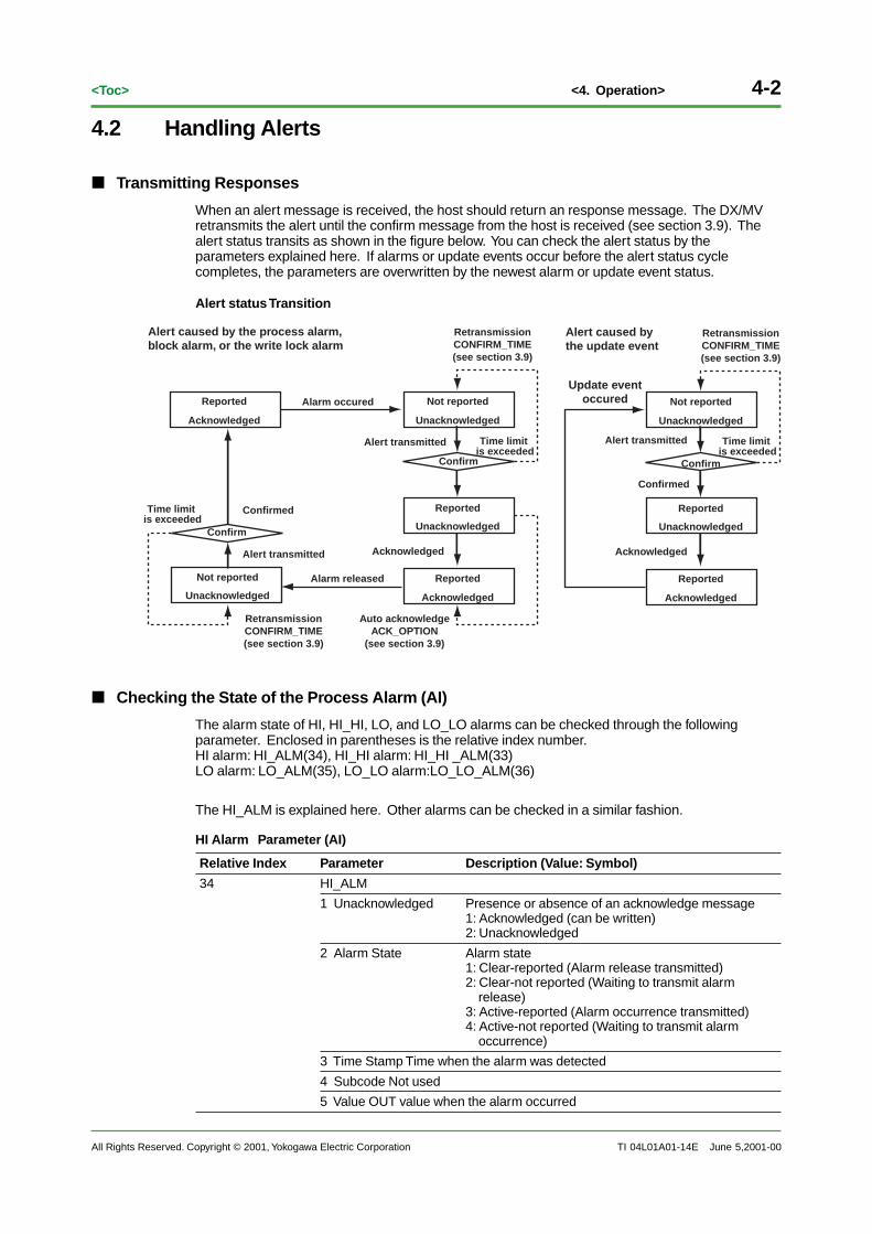
4-2
All Rights Reserved. Copyright © 2001, Yokogawa Electric Corporation
<Toc>
TI 04L01A01-14E
<4. Operation>
June 5,2001-00
4.2 Handling Alerts
■ Transmitting Responses
When an alert message is received, the host should return an response message. The DX/MVretransmits the alert until the confirm message from the host is received (see section 3.9). Thealert status transits as shown in the figure below. You can check the alert status by theparameters explained here. If alarms or update events occur before the alert status cyclecompletes, the parameters are overwritten by the newest alarm or update event status.
Alert status Transition
Alarm occured
Alarm released
Not reported
Not reported
Unacknowledged
Unacknowledged
Reported
Acknowledged
Reported
Acknowledged
Unacknowledged
AcknowledgedAlert transmitted
Confirmed
Alert caused by the process alarm, block alarm, or the write lock alarm
RetransmissionCONFIRM_TIME(see section 3.9)
RetransmissionCONFIRM_TIME(see section 3.9)
Auto acknowledgeACK_OPTION
(see section 3.9)
Alert transmitted
Confirm
Time limit is exceeded
Time limit is exceeded
Reported
Confirm
Update eventoccured Not reported
Unacknowledged
Reported
Acknowledged
Unacknowledged
Acknowledged
Alert transmitted
Confirmed
Alert caused by the update event
Confirm
Time limit is exceeded
Reported
RetransmissionCONFIRM_TIME(see section 3.9)
■ Checking the State of the Process Alarm (AI)
The alarm state of HI, HI_HI, LO, and LO_LO alarms can be checked through the followingparameter. Enclosed in parentheses is the relative index number.HI alarm: HI_ALM(34), HI_HI alarm: HI_HI _ALM(33)LO alarm: LO_ALM(35), LO_LO alarm:LO_LO_ALM(36)
The HI_ALM is explained here. Other alarms can be checked in a similar fashion.
HI Alarm Parameter (AI)
Relative Index Parameter Description (Value: Symbol)
34 HI_ALM
1 Unacknowledged Presence or absence of an acknowledge message1: Acknowledged (can be written)2: Unacknowledged
2 Alarm State Alarm state1: Clear-reported (Alarm release transmitted)2: Clear-not reported (Waiting to transmit alarm release)3: Active-reported (Alarm occurrence transmitted)4: Active-not reported (Waiting to transmit alarm occurrence)
3 Time Stamp Time when the alarm was detected
4 Subcode Not used
5 Value OUT value when the alarm occurred

All Rights Reserved. Copyright © 2001, Yokogawa Electric Corporation TI 04L01A01-14E
4-3<Toc> <4. Operation>
June 5,2001-00
■ Checking the State of the Block Alarm (RB, TB, AI, MAI, MAO)
Checking the Alarm State
You can check the block alarm state through
Block Alarm Parameter (RB, TB, AI, MAI, and MAO)
Relative Index Parameter Description (Value: Symbol)
RB: 36 BLOCK_ALM
TB: 8 1 Unacknowledged Presence or absence of an acknowledge messageAI: 21 1: Acknowledged (can be written)MAI: 17 2: Unacµowledged
MAO: 28 2 Alarm State Alarm state1: Clear-reported (Alarm release transmitted)2: Clear-not reported (Waiting to transmit alarm release)3: Active-reported (Alarm occurrence transmitted)4: Active-not reported (Waiting to transmit alarm occurrence)
3 Time Stamp Time when the alarm was detected
4 Subcode BLOCK_ERR value
5 Value Not used
Checking the Alarm Information
You can check the alarm information through the BLOCK_ERR value of each block. For detailson the BLOCK_ERR values, see section 5.2.
Parameter Indicating the Block Alarm Information (RB, TB, AI, MAI, and MAO)
Relative Index Parameter
6 BLOCK_ERR
■ Checking the State of the Write Lock Alarm
You can check the state of the write lock alarm through WRITE_ALM of the resource block.
Write Lock Alarm Parameter (RB)
Relative Index Parameter Description (Value: Symbol)
40 WRITE_ALM
1 Unacknowledged Presence or absence of an acknowledge message1: Acknowledged2: Unacknowledged
2 Update State Write lock alarm state1: Clear-reported (Write lock release transmitted)2: Clear-not reported (Waiting to transmit write lock release)3: Active-reported (Write lock enable transmitted)4: Active-not reported (Waiting to transmit write lock enable)
3 Time Stamp Time when the write lock alarm occurred
4 Subcode Not used
5 Value WRITE_LOCK value when the write lock alarmoccurred

4-4
All Rights Reserved. Copyright © 2001, Yokogawa Electric Corporation
<Toc>
TI 04L01A01-14E
<4. Operation>
June 5,2001-00
■ Checking the State of the Update Event
You can check the state of the update event through UPDATE_EVT of each block. While the blockmode is OOS (the value of Actual of MODE_BLK is OOS), no alert will be transmitted even if theparameters are written. The retained alert will be transmitted when the block goes out of OOSmode.
Update Event Parameter (RB, TB, AI, MAI, and MAO)
Relative Index Parameter Description (Value: Symbol)
RB: 35 UPDATE_EVT
TB: 7 1 Unacknowledged Presence or absence of an acknowledge messageAI: 20 1: Acknowledged (can be written)MAI: 16 2: Unacknowledged
MAO: 27 2 Update State Update event state1: Update-reported (Update event transmitted)2: Update-not reported (Waiting to transmit update event)
3 Time Stamp Time when the update event occurred
4 Static Revision Revision value of the static parameter when the updateevent occurred (ST_REV value)
5 Relative Index Relative index number of the updated parameter.However, the value is set to 0 when an update eventoccurs as a result of updating multiple parameterssimultaneously.
■ Checking through the Alarm Summary
You can check the state of all the alarms of the RB, TB, or AI function block through ALARM_SUMof each block.
Alarm Summary Parameter (RB, TB, and AI)
Relative Index Parameter Description (Value: Symbol)
RB: 37 ALARM_SUM
TB: 16 1 Current Indicates the alarm that is currently occurring
AI: 22 2 Unacknowledged Indicates the alarms that have not received anacknowledge message from the host in response to thealarm transmission
3 Unreported Indicates the alarms which have not been transmitted
4 Disabled Sets whether to generate the alarm (see section 3.9)
The alarm type is indicated using a two-byte bit sequence. The alarm corresponding to the bitthat is set to 1 is the alarm that meets the above conditions.
ALARM_SUM Value
Bit Symbol Description
0 Discrete alarm WRITE_LOCK
1 High high alarm HI_HI_ALM
2 High alarm HI_ALM
3 Low low alarm LO_LO_ALM
4 Low alarm LO_ALM
5 - Not used
6 - Not used
7 Block alarm BLOCK_ALM
8 to 15 - (Reserved)

All Rights Reserved. Copyright © 2001, Yokogawa Electric Corporation TI 04L01A01-14E
4-5<Toc> <4. Operation>
June 5,2001-00
4.3 Using the Using the Simulation Function (AI Function Block)The AI function block is capable of outputting a manually specified value in place of the actualvalue from the sensor.
When the simulation function is not in use, the value received from the transducer block istransmitted to FIELD_VAL and PV through SIMULATE.
SIMULATE Parameter
SIMULATE
FIELD_VALPV
Transducer
Simulate
Enable/Disable
Resource BlockBLOCK_ERR
Simulation Jumper
CHANNELTransducer Block
■ Turning ON the Simulation Jumper
To use the simulation function, turn ON the Simulation Jumper. A block alarm is generated fromthe resource block (Simulate Active (bit 3) of the BLOCK_ERR parameter is set to 1) and thesimulation function is enabled.There are two methods in turning ON the Simulation Jumper.
Turning ON the SimEnable TerminalShort the SimEnable terminal on the rear panel of the DX/MV and the FG terminal. For details onthe SimEnable terminal, see section 2.2.
Using the SIM_ENABLE_MSG Parameter
Parameter for Turning ON the Simulation Jumper (RB)
Relative Index Parameter Write Mode
44 SIM_ENABLE_MSG All modes
Specifying “REMOTE_LOOP_TEST_SWITCH” (all capitals, “_” indicates a space) to thisparameter turns ON the Simulation Jumper. However, this setting is lost when the power is turnedOFF.

4-6
All Rights Reserved. Copyright © 2001, Yokogawa Electric Corporation
<Toc>
TI 04L01A01-14E
<4. Operation>
June 5,2001-00
■ Outputting Simulation Values
Setting Whether to Output Simulation Values
Set whether to output simulation values through Enable/Disable of SIMULATE of the AI functionblock.
Parameter for Setting the Simulation (AI)
Relative Index Parameter Description (Value: Meaning)
9 SIMULATE
1 Simulate Status Status value* when simulation is enabled
2 Simulate Value Process value when simulation is enabled
3 Transducer Status Status value from the transducer block.You cannot change this value.
4 Transducer Value Process value from the transducer block.You cannot change this value.
5 Enable/Disable Controls the enable/disable of the simulation1: Simulation disabled2: Simulation enabled
* For details on the status values, see section 5.1.
Setting the Simulation Value
Simulation value is set through SIMULATE of the AI function block. The relationship between thespecified simulation value and the output value is expressed by the equation given in “ProcessProcedure of the Measured/Computed Data” in section 3.5.
Note
• The specified simulation value can only be output when the simulation jumper is ON andEnable/Disable of SIMULATE is set to 2 (Enable). If this condition is not satisfied, the valuefrom the resource block is output.
• When the simulation function is not used, the values from the transducer block are copied toSimulation Value and Simulation Status.

All Rights Reserved. Copyright © 2001, Yokogawa Electric Corporation TI 04L01A01-14E
4-7<Toc> <4. Operation>
June 5,2001-00
4.4 Checking the Status of the Communication Input DataThe PD tag, node address, and the status of the process value that the MAO function block of theDX/MV has retrieved from the fieldbus can be confirmed on the
■ FIELDBUS DATA Screen
For the items displayed at Quality, Sub-status, and Limit and their meanings, see “Status andValue of the Input Parameter” in section 5.1.
PD tag of the DX/MV
Quality sub status (see section 5.1)Quality of the communication data (see section 5.1)
Communication input data that is linked (see section 3.7)
Node address of the DX/MV
Limit (see section 5.1)
■ Procedure in Displaying the Status Screen
1. Press the FUNC key of the DX/MV. The FUNC menu appears.
2. Press the Fieldbus soft key. The FIELDBUS DATA screen appears.

Blank Page

All Rights Reserved. Copyright © 2001, Yokogawa Electric Corporation TI 04L01A01-14E
5-1<Toc> <5. Troubleshooting>
June 5,2001-00
5. Troubleshooting
5.1 Handling the I/O StatusWhen correct data are not displayed on the DX/MV or the host, the cause can be identified bychecking the data processing process one by one in the reverse order to the publisher. In thatcase, Status of I/O parameters has useful information. For how to use Status of I/O parameters,see an example on the latter part of this section.
■ I/O Parameter Status
Applicable Parameters
The following parameters have two values, Status and Value.
Parameters That Have Status and value
Parameter Description
PV AI-1 through AI-8 function blocks
OUT AI-1 through AI-8 function blocks
SIMULATE AI-1 through AI-8 function blocksThe following parameters of SIMULATE• Simulate Status, Simulate Value• Transducer Status, Transducer Value
FIELD_VAL AI-1 through AI-8 function blocks
OUT-1 to OUT-8 MAI function block
IN-1 to IN-8 MAO function block
Status Structure
Status consists of Quality, Quality Sub-status, and Limit. It indicates the status of Value. Statususes the 8 bits as shown in the following figure .
7Status
6 5 4 3 2 1 0Quality Quality Sub-status Limit

5-2
All Rights Reserved. Copyright © 2001, Yokogawa Electric Corporation
<Toc>
TI 04L01A01-14E
<5. Troubleshooting>
June 5,2001-00
Value and Meaning of Quality and Quality Sub-status
Quality and Quality Sub-status have the following values and meanings. The values andmeanings that the I/O parameters of the DX/MV can have, and corrective action to them, seepages 5-4 and 5-5.
Quality and Quality Sub-status (when the quality value is “0.”)
Quality Value Quality Indication (Top Row) and Meaning (Bottom Row)
0 BadValue is invalid.
Sub-status Value Sub-status Indication (Top Row) and Meaning (Bottom Row)
0 Non-specificThe cause cannot be determined.
1 Configuration ErrorA problem exists in the FB.
2 Not ConnectedNo connection to the input.
3 Device FailureThe value is influenced by device failure.
4 Sensor FailureThe value has exceeded the limits of the device.
5 No communication, with last usable valueFailed to communicate the value.
6 No communication, with no usable valueNo value has been communicated after the last OOS.
7 Out of ServiceThe value is unreliable because the FB is not operating.
Quality and Quality Sub-status (when the quality value is “1.”)
Quality Value Quality Indication (Top Row) and Meaning (Bottom Row)
1 UncertainThe quality of Value is inferior as compared to the normal case, but it may be used.
Sub-status Value Sub-status Indication (Top Row) and Meaning(Bottom Row)
0 Non-specificThe cause cannot be determined.
1 Last Usable Value*The remote device that was writing the value stopped theoperation.
2 SubstituteThe value was written when the FB was not OOS.
3 Initial ValueThe input has not changed since the value was written whenthe FB was OOS.
4 Sensor Conversion not AccurateThe value has exceeded the limits of the sensor or theprecision of the sensor is not appropriate.
5 Engineering Unit Range ViolationThe value has exceeded the range of values that has beendefined with an engineering unit.
6 Sub-normalValue that has been generated without the required number ofinformation.
* This occurs when the input is disconnected by the configurator.

All Rights Reserved. Copyright © 2001, Yokogawa Electric Corporation TI 04L01A01-14E
5-3<Toc> <5. Troubleshooting>
June 5,2001-00
Quality and Quality Sub-status (when the quality value is “2.”)
Quality Value Quality Indication (Top Row) and Meaning (Bottom Row)
2 Good (Non-Cascade)Value is invalid.
Sub-status Value Sub-status Indication (Top Row) and Meaning(Bottom Row)
0 Non-specificThe cause cannot be determined.
1 Active Block AlarmAn active block alarm exists.
2 Active Advisory AlarmAn alarm with a priority less than 8 is occurring.
3 Active Critical AlarmAn alarm with a priority greater than or equal to 8 is occurring.
4 Unacknowledged Block AlarmA block alarm that has not received an acknowledge messagefrom the host exists.
5 Unacknowledged Advisory AlarmAn alarm with a priority less than 8 that has not received anacknowledge from the host exists.
6 Unacknowledged Critical AlarmAn alarm with a priority greater than or equal to 8 that has notreceived an acknowledge from the host exists.
Quality and Quality Sub-status (when the quality value is “3.”)
Quality Value Quality Indication (Top Row) and Meaning (Bottom Row)
3 Good (Cascade)Value is valid and can be used for control.
Sub-status Value Sub-status Indication (Top Row) and Meaning(Bottom Row)
0 Non-specificThe cause cannot be determined.
1 Initialization Acknowledged (IA)The value is set to the initial value on the source side.
2 Initialization Request (IR)*The value is set to the initial value on the source side.
3 Not Invited (NI)Value from the FB that is not looping back this input.
4 Not Selected (NS)Value from the selected Control Selector that is not loopingback this input.
5 = Reserved 6 = Local Override (LO)Value that has been overwritten by the internal logic of the FB.
7 Fault State Active (FSA)Value from the FB of which Fault State is Active.
8 Initial Fault State (IFS)Value from the FB that is requesting the FB on the datareceiving side to become “Fault State.”
* This occurs when the downstream side of the control loop is disconnected.

5-4
All Rights Reserved. Copyright © 2001, Yokogawa Electric Corporation
<Toc>
TI 04L01A01-14E
<5. Troubleshooting>
June 5,2001-00
Value and Meaning of Limit
Limit
Limit Value Limit Indication (Top Row) and Meaning (Bottom Row)
0 Not limitedThe value can change freely.
1 Low limitedThere is a lower limit placed on the value.
2 High limitedThere is an upper limit placed on the value.
3 Constant (high and low limited)The value cannot change.
OUT (AI) Status and Corrective Actions
Quality Sub status Limit Cause Corrective Action/Reference Section
Bad Non-specific Not limited The connected channel is Check AI_MAP value (sectionnot correct. 3.5), or see chapters 5 and 11 of the
DX/MV’s User’s Manual.
The connected channel See chapter 5 of the DX/MV’s Manual.is skipped.
Bad Device Failure Not limited Internal error Check DEVICE_STATUS (section 5.3).
Bad Sensor Failure Not limited The sensor has burned out. Check the sensor.
Error data See chapters 5 and 11 of the DX/ MV’sInvalid data User’s Manual.Positive/negative overrange, positivePositive/negative overrange, computation over display range
Bad Out of Service Not limited The RB is in OOS mode. 3.4
EEPROM failure Check DEVICE_STATUS (section 5.3).
TB or AI is in OOS mode. 3.4
Good (Non-Cascade) Not limited Data is validNon-specific
Good (Non-Cascade) Not limited Data is valid An active block alarm exists. 4.2Active Block Alarm
Good (Non-Cascade) Not limited Data is valid Alarm with a priority less than 8 isActive Advisory Alarm occurring. 4.2
Good (Non-Cascade) Not limited Data is valid Alarm with a priority greater than orActive Critical Alarm equal to 8 is occurring. 4.2
Good (Non-Cascade) Not limited Data is valid A block alarm that has not receivedUnacknowledged Block Alarm an acknowledge message from the
host exists. 4.2
Good (Non-Cascade) Not limited Data is valid An alarm with a priority less than 8Unacknowledged Advisory Alarm that has not received an acknowledge from
the host exists. 4.2
Good (Non-Cascade) Not limited Data is valid An alarm with a priority greater thanUnacknowledged Critical Alarm or equal to 8 that has not received an
acknowledge from the host exists. 4.2

All Rights Reserved. Copyright © 2001, Yokogawa Electric Corporation TI 04L01A01-14E
5-5<Toc> <5. Troubleshooting>
June 5,2001-00
FIELD_VAL (AI) Status and Corrective Actions (when the simulation function is not in use)
Quality Sub status Limit Cause Corrective Action/Reference Section
Bad Non-specific Not limited The RB is in OOS mode. 3.4
EEPROM failure Check DEVICE_STATUS (section 5.3).
Bad Configuration Error Not limited The connected channel is Check AI_MAP value (section 3.5), or seenot correct. chapters 5 and 11 of the DX/MV’s User’s Manual.
The connected channel is See chapter 5 of the DX/MV’sskipped. User’s Manual.
Bad Device Failure Not limited Internal error Check DEVICE_STATUS (section 5.3).
Bad Sensor Failure Not limited The sensor has burned out. Check the sensor.Error data See chapters 5 and 11 of the DX/MV’sInvalid data User’s Manual.Positive/negative overrange,positivePositive/negative computation over display range
Bad Out of Service Not limited TB or AI is in OOS mode. 3.4
Good (Non-Cascade) Not limited Data is valid
Non-specific
Status of OUT_1 though OUT_8 (MAI) and corrective Actions
Quality Sub status Limit Cause Corrective Action/Reference Section
Bad Configuration Error Not limited The connected channel is See chapters 5 and 11 of the DX/MV’snot correct. User’s Manual.
The connected channel is See chapter 5 of the DX/MV’sskipped. User’s Manual.
Bad Device Failure Not limited Internal error Check DEVICE_STATUS (section 5.3).
Bad Sensor Failure Not limited The sensor has burned out. Check the sensor.
Error data See chapters 5 and 11 of the DX/MV’sInvalid data User’s Manual.Positive/negative overrange, positivePositive/negative computation over display range
Bad Out of Service Not limited The RB or AI is in OOS mode. 3.4
EEPROM failure Check DEVICE_STATUS(section 5.3).
TB or AI is in OOS mode. 3.4
Good (Non-Cascade) Not limited Data is validNon-specific
Good (Non-Cascade) Not limited Data is valid An active block alarm exists. 4.2Active Block Alarm
Good (Non-Cascade) Not limited Data is valid A block alarm that has not received anUnacknowledged Block Alarm acknowledge message from the host exists.
4.2

5-6
All Rights Reserved. Copyright © 2001, Yokogawa Electric Corporation
<Toc>
TI 04L01A01-14E
<5. Troubleshooting>
June 5,2001-00
■ Status of IN_1 through IN _8(MAO)
IN-1 through IN-8 are data that is received externally. Determine the quality of the data byreferring to the value and meaning of Quality and Quality Sub-status in the “Input ParameterStatus” section.
■ Value of Input/Output Parameters
Value is a floating-point decimal that can take on the values in the range in the white area in thefollowing figure. In addition to this range, there is also a range of values that the measurementand computation channels of the DX/MV can handle. For information on this range, see the DX/MV’s User’s Manual.
If the value on the measurement channel becomes ±overrange or the value on the computationchannel becomes ±over display range in the processing of the DX/MV, the value±OVER(±1.0E+37) is passed to the transducer block.
7f 80 00 00
:
7c f0 bd c2
:
:
fc f0 bd c2
:
ff 80 00 00
+INF
+OVER
+INF
+1.0E+37
−1.0E+37
−INF
−OVER
−INF
Number range that the computation channel of the DX/MV can handle (−9999999 to +99999999)
Number range that measurement channel of the DX/MV can handle

All Rights Reserved. Copyright © 2001, Yokogawa Electric Corporation TI 04L01A01-14E
5-7<Toc> <5. Troubleshooting>
June 5,2001-00
■ An Example Explaining How to Use Status of I/O Parameters
The figure shows the case in which the data retrieved from AI function block OUT of the DX/MV iserroneous.
Status of I/O Parameters
Function block
Measurement/computation
channel TB
DX or MV
Incorrect values
AI
CHANNEL
12356
OUT Status Value
FIELD_VAL Status Value
AI_MAPMeasured value
Computed value
IN Status Valueor
Field device
4
Start from the step No.1 in the figure. If the cause is not identified, go to the next step.
1. Checking Value and Status of IN of the field device
See the user’s manual for the field device.
2. Checking Value and Status of AI function block OUT
• Status is “Good (Non-Cascade)”
If the Status is “Good (Non-Cascade)” and the Value is correct, the problem exists afterthe AI function block (communication via fieldbus in this case).
• Status is “Bad”
If the Status is “Bad,” check the information through the Sub-Status value.
• Status is “Bad” and Sub-Status is “Non-specific”
The resource block is not set to Auto mode. Set the block mode of the resourceblock to Auto (see section 3.4).
• Status is “Bad” and Sub-Status is “Sensor Failure” and Limit is “High”
If the AI function block OUT is connected to the measurement channel of the DX/MV, positive over range is occurring. Check the input signal to the measurementchannel.
If the AI function block OUT is connected to the computation channel of the DX/MV,positive over display range is occurring. Check the equation or the data used in theequation.
Check the Sub-Status and Limit value in the similar fashion as described above, andtake proper corrective actions.

5-8
All Rights Reserved. Copyright © 2001, Yokogawa Electric Corporation
<Toc>
TI 04L01A01-14E
<5. Troubleshooting>
3. Checking Value and Status of AI function block FIELD_VAL
• Status is “Good (Non-Cascade)”
If the Status is “Good (Non-Cascade)” and the Value is correct, the problem exists in thedata processing after FIELD_VAL.
• Status is “Bad”
If the Status is “Bad,” check the information through the Sub-Status value.
• Status is “Bad” and Sub-Status is “Non-specific”
The resource block is not set to Auto mode. Set the block mode of the resourceblock to Auto (see section 3.4).
Check the Sub-Status and Limit value in the similar fashion as described above, andtake proper corrective actions.
4., 5., 6.
Check the settings of CHANNEL of the AI function block, AI_MAP of the transducer block,and the measurement/computation channel.
June 5,2001-00

All Rights Reserved. Copyright © 2001, Yokogawa Electric Corporation TI 04L01A01-14E
5-9<Toc> <5. Troubleshooting>
5.2 HandlingYou can check the cause of the block alarm of a function block through BLOCK_ERR of eachblock. For the transducer block, also check the XD_ERROR value, which indicates “transducer” *error.
* Transducers are components of the transducer block.
Parameter Indicating Block Error (RB, TB, AI, MAI, and MAO)
Relative Index No. Parameter
6 BLOCK_ERR
Parameter Indicating the Information of the Transducer Error (TB)
Relative Index No. Parameter
11 XD_ERROR
BLOCK_ERR information is expressed using a two-byte bit sequence. The block alarmcorresponding to the bit that is set to 1 is occurring. The cause of the block alarm of each functionblock is shown below.
■ Resource Block
Only the used bits are indicated.
BLOCK_ERR Value and Corrective Action
Bit Indication Description Corrective Action/Reference Section
3 Simulate Active Simulation Jumper is ON 4.3
5 Device Fault State Set FAULT_STATE of the RB is active 3.7
10 Lost Static Data Internal error Check DEVICE_STATUS (section 5.3).
11 Lost NV Data Internal error Check DEVICE_STATUS (section 5.3).
13 Device Needs Maintenance Now Internal error Check DEVICE_STATUS (section 5.3).
15 Out of Service RS_STATE is not “Online,” or Target. 3.4 and “States and Transition of the ResourceMODE_BLK is OOS. Block” in this section
■ Transducer Block
Only the used bits are indicated.
BLOCK_ERR Value and Corrective Action
Bit Indication Description Corrective Action/Reference Section
7 Input Failure Internal error Check DEVICE_STATUS (section 5.3).
8 Output Failure Internal error Check DEVICE_STATUS (section 5.3).
13 Device Needs Maintenance Now Internal error Check DEVICE_STATUS (section 5.3).
15 Out of Service RS_STATE is not “Online,” or Target. 3.4 and “States and Transition of the ResourceMODE_BLK is OOS. Block” in this section
XD_ERROR takes the following values.
XD_ERROR Value and Corrective Action
Value Indication Description Corrective Action/Reference Section
20 Electronic failure Internal error Check DEVICE_STATUS (section 5.3).
22 I/O failure Internal error Check DEVICE_STATUS (section 5.3).
June 5,2001-00

5-10
All Rights Reserved. Copyright © 2001, Yokogawa Electric Corporation
<Toc>
TI 04L01A01-14E
<5. Troubleshooting>
■ AI Function Block
Only the used bits are indicated.
BLOCK_ERR Value and Corrective Action
Bit Indication Description Corrective Action/Reference Section
1 Block Configuration Error The CHANNEL value of 3.4the FB is not correct.
3 Simulate Active Simulate Enable/Disable 4.3of SIMULATEof the AI is setto Enable
7 Input Failure Internal error Check DEVICE_STATUS (section 5.3).
15 Out of Service The MODE_BLK Target of 3.4 the RB or AI is OOS.
■ MAI Function Block
Only the used bits are indicated.
BLOCK_ERR Value and Corrective Action
Bit Indication Description Corrective Action/Reference Section
1 Block Configuration Error The CHANNEL value of 3.6the FB is not correct.
7 Input Failure Internal error Check DEVICE_STATUS (section 5.3).
15 Out of Service The MODE_BLK Target of the RB 3.4or MAI is OOS.
■ MAO Function Block
Only the used bits are indicated.
BLOCK_ERR Value and Corrective Action
Bit Indication Description Corrective Action/Reference Section
1 Block Configuration Error The CHANNEL value of 3.6the FB is not correct.
4 Local Override Actual of MODE_BLK of Fault State condition. 3.4 and 3.7the MAO is Local Override (LO).
8 Output Failure Internal error Check DEVICE_STATUS (section 5.3).
15 Out of Service The MODE_BLK Target of the RB 3.4or MAO is OOS.
June 5,2001-00

All Rights Reserved. Copyright © 2001, Yokogawa Electric Corporation TI 04L01A01-14E
5-11<Toc> <5. Troubleshooting>
■ States and Transition of the Resource Block
The following figure shows the various states of the resource block.
States of the Resource Block
All states1. Start/Restart
2. Initialization
3. Online linking
4. Online
6. Failure
5. Stand by
Start/RestartThis is the state at the time the DX/MV is started or restarted. An initial check is executed, andupon success, transition is made to Initialization.
InitializationThe node address is not specified in this state. The function block does not operate. When thenode address is set and the block mode is set to Auto, transition is made to Online or Onlinelinking state.When the node address is set and the block mode is set to OOS, transition is made to Stand by.
Online linkingThis is the state in which the block mode is set to Auto and the block mode is runningautomatically. However, there is one or more VCRs used in the communication that are notopened, and their links are not established. When the link is established, the transition is made toOnline.If the node address is cleared, the state returns to Initialization.
OnlineThis is the state in which the block mode is set to Auto and the block is running automatically.If the node address is cleared, the state returns to Initialization.
Stand byThis is the state in which the block mode is OOS, and the resource block is in a state other thanFailure. When the block mode is set to Auto, transition is made to Initialization, Online linking, orOnline.
FailureIf the result of self diagnosis in any state is failure, transition is made to Failure. After transmittinga block alarm, the parameters of all function blocks are reset to their initial values. The DX/MVhas malfunctioned.
June 5,2001-00

5-12
All Rights Reserved. Copyright © 2001, Yokogawa Electric Corporation
<Toc>
TI 04L01A01-14E
<5. Troubleshooting>
■ Checking the State of the Resource Block
The RS_STATE parameter of the resource block can be used to check the state of the resourceblock.
Parameter That Indicates the State of the Resource Block (RB)
Relative Index No. Parameter Description
7 RS_STATE The state is indicated using an 8-bit unsigned integer(read only).
The correspondence between the bits and states are as follows:
RS_STATE Value
Value State
1 Start/Restart
2 Initialization
3 Online linking
4 Online
5 Stand by
6 Failure
June 5,2001-00

All Rights Reserved. Copyright © 2001, Yokogawa Electric Corporation TI 04L01A01-14E
5-13<Toc> <5. Troubleshooting>
5.3 Handling the Device Status (DEVICE_STATUS)
■ Displaying the Status
You can check the status of the DX/MV through DEVICE_STATUS_1 to DEVICE_STATUS_8 ofthe resource block.
Parameter for Confirming the DX/MV Status (RB)
Relative Index No. Parameter Description
45 DEVICE_STATUS_1 Status of the RB and VCR
46 DEVICE_STATUS_2 Status of the TB and the identification information ofthe DX/MV
47 DEVICE_STATUS_3 Status of AI-1 to AI-8
48 DEVICE_STATUS_4 Status of the MAI
49 DEVICE_STATUS_5 Status of the MAO
50 DEVICE_STATUS_6 Not used
51 DEVICE_STATUS_7 Not used
52 DEVICE_STATUS_8 Not used
The value of each parameter is a four-byte bit sequence. The correspondence between the bitsand statuses and the corrective actions are shown below. When the bit value is 1, the DX/MV is inthe described status.
■ DEVICE_STATUS_1
Only the used bits are indicated.
DEVICE_STATUS_1 Value and Corrective Action
Bit Indication Description Corrective Action/Reference Section
23 Sim.enable Jmpr On Simulation Jumper is ON 4.3
22 RB in OOS mode MODE_BLK.ACTUAL of the RB is OOS 3.4
19 EEPROM failure Problems in the non-volatile memory Contact your nearest YOKOGAWA(EEPROM). dealer.
15 Link Obj.1/17 not open The VCR corresponding to 3.11the VCR Number of the LinkObject is not open.
14 Link Obj.2/18 not open Same as above Same as above
13 Link Obj.3/19 not open Same as above Same as above
12 Link Obj.4/20 not open Same as above Same as above
11 Link Obj.5/21 not open Same as above Same as above
10 Link Obj.6/22 not open Same as above Same as above
9 Link Obj.7/23 not open Same as above Same as above
8 Link Obj.8/24 not open Same as above Same as above
7 Link Obj.9/25 not open Same as above Same as above
6 Link Obj.10/26 not open Same as above Same as above
5 Link Obj.11/27 not open Same as above Same as above
4 Link Obj.12/28 not open Same as above Same as above
3 Link Obj.13/29 not open Same as above Same as above
2 Link Obj.14/30 not open Same as above Same as above
1 Link Obj.15/31 not open Same as above Same as above
0 Link Obj.16/32 not open Same as above Same as above
June 5,2001-00

5-14
All Rights Reserved. Copyright © 2001, Yokogawa Electric Corporation
<Toc>
TI 04L01A01-14E
<5. Troubleshooting>
■ DEVICE_STATUS_2
Only the used bits are indicated.
DEVICE_STATUS_2 Value and Corrective Action
Bit Indication Description Corrective Action/Reference Section
30 DEVICE_ID failure Invalid DEVICE_ID. Contact your nearest YOKOGAWA dealer.
29 REVISION failure Invalid DEV_TYPE, DEV_REV, Contact your nearest YOKOGAWA dealer.or DD_REV.
28 UART failure Problems in the internal Contact your nearest YOKOGAWA dealer.communication (UART).
15 TB in O/S mode MODE_BLK.ACTUAL of the TB is OOS. 3.4
■ DEVICE_STATUS_3
Only the used bits are indicated.
DEVICE_STATUS_3 Value and Corrective Action
Bit Indication Description Corrective Action/Reference Section
30 AI-1 in O/S mode MODE_BLK.ACTUAL of AI-1 is OOS. 3.4
29 AI-2 in O/S mode MODE_BLK.ACTUAL of AI-2 is OOS. 3.4
28 AI-3 in O/S mode MODE_BLK.ACTUAL of AI-3 is OOS. 3.4
27 AI-4 in O/S mode MODE_BLK.ACTUAL of AI-4 is OOS. 3.4
26 AI-5 in O/S mode MODE_BLK.ACTUAL of AI-5 is OOS. 3.4
25 AI-6 in O/S mode MODE_BLK.ACTUAL of AI-6 is OOS. 3.4
24 AI-7 in O/S mode MODE_BLK.ACTUAL of AI-7 is OOS. 3.4
23 AI-8 in O/S mode MODE_BLK.ACTUAL of AI-8 is OOS. 3.4
15 AI-1 not scheduled AI-1 is not scheduled. 3.12
14 AI-2 not scheduled AI-2 is not scheduled. 3.12
13 AI-3 not scheduled AI-3 is not scheduled. 3.12
12 AI-4 not scheduled AI-4 is not scheduled. 3.12
11 AI-5 not scheduled AI-5 is not scheduled. 3.12
10 AI-6 not scheduled AI-6 is not scheduled. 3.12
9 AI-7 not scheduled AI-7 is not scheduled. 3.12
8 AI-8 not scheduled AI-8 is not scheduled. 3.12
■ DEVICE_STATUS_4
Only the used bits are indicated.
DEVICE_STATUS_4 Value and Corrective Action
Bit Indication Description Corrective Action/Reference Section
30 MAI-1 in O/S mode MODE_BLK.ACTUAL of MAI-1 is OOS. 3.4
15 MAI-1 not scheduled MAI-1 is not scheduled. 3.12
■ DEVICE_STATUS_5
Only the used bits are indicated.
DEVICE_STATUS_5 Value and Corrective Action
Bit Indication Description Corrective Action/Reference Section
30 MAO-1 in O/S mode MODE_BLK.ACTUAL of MAO-1 is OOS. 3.4
15 MAO-1 not scheduled MAO-1 is not scheduled. 3.12
June 5,2001-00

All Rights Reserved. Copyright © 2001, Yokogawa Electric Corporation TI 04L01A01-14E
5-15<Toc> <5. Troubleshooting>
5.4 Troubleshooting the
■ When the Scheduler Stops, the DX/MV Does Not Transit to Scheduler
1. Check that the DX/MV is configured as an link master device.
Check that the BOOT_OPERAT_FUNCTIONAL_CLASS (MIB, index number 367) value isset to 2 (Link Master, see section 3.13).
2. Check that the node address of the DX/MV is smaller than other link master devices.
This Node value of DLME_BASIC_INFO (MIB, index number 361) indicates the nodeaddress.(see section 3.2).
■ Would Like to Transit the DX/MV to Scheduler while the Scheduler Is in Operation
1. Check that the version number of the schedule in execution matches between thescheduler in operation and the DX/MV.
On the DX/MV, the Active Schedule Version value ofLINK_SCHEDULE_LIST_CHARACTERISTICS_RECORD (MIB, index number 374) is theschedule version number (see the explanation ofLINK_SCHEDULE_LIST_CHARACTERISTICS_RECORD in appendix 2).
2. Declare the DX/MV to become the scheduler
First, set the PRIMARY_LINK_MASTER_FLAG_VARIABLE parameter of the scheduler inoperation to 0x00 (false).
Then, set PRIMARY_LINK_MASTER_FLAG_VARIABLE (MIB, index number 364) of theDX/MV to 0xff (true).
■ Other Devices Cannot Be Connected to the Fieldbus on Which the DX/MV is Operating asthe Scheduler
1. Check that the following parameter value of the DX/MV is greater than the parametervalue of the device to be connected.
DX/MV Device to Be Connected
V(ST) > V(ST)
V(MID) > V(MID)
V(MRD) > V(MRD)
• DX/MV parameterThe Slot Time value (subindex number 1) ofCONFIGURED_LINK_SETTING_RECORD (MIB, index number 369) is V(ST). TheMin Inter Pdu Delay value is V(MID). The MAX Response Delay value is V(MRD).
• Parameter of the device to be connectedThe Slot Time value of DLME_BASIC_INFO is V(ST). The Min Inter Pdu Delay value isV(MID). The MAX Response Delay value is V(MRD).
2. Check that the node address of the device to be connected is included in the nodeaddress range to be used specified by the DX/MV.
For the procedure in setting the node address range to be used, see section 3.14.

Blank Page
June 5,2001-00

All Rights Reserved. Copyright © 1996, Yokogawa Electric Corporation TI 04L01A01-14E
App.-1<Toc> <Appendix 1. Terminology>
June 5,2001-00
Appendix 1 Terminology
■ Basic Device
Basic device is a field deice that does not have scheduler functionality. There can be multiplebasic devices on a single fieldbus.
■ Communication Types (Client/Server)
The device that wishes to communicate (client) transmits a message to the destination device(server) when it receives permission from the scheduler. The server does not respondimmediately; it responds when it receives permission from the scheduler.
• This type of communication is used for unscheduled communications such as thedownloading of all the parameters of a device.
• It is one to one communication.
• The messages are transmitted or received in order without a loss or overwriting.
Client Scheduler
ClientScheduler
Fieldbus
Server
Service request (when permitted by the scheduler)
Response (when permitted by the scheduler)2
1
■ Communication Types (Publisher/Subscriber)
The device (publisher) that receives a transmit request from the scheduler broadcasts the data toall devices on the fieldbus. Devices that are set to receive the data (subscriber) saves the data.
• This type of communication is used for scheduled, cyclic data transfers.
• It is one to many communications.
• A scheduler issues the data transfer request.
• The subscriber saves only the latest version of the data. New data overwrites
Publisher/Subscriber
SubscriberScheduler
Fieldbus
Publisher Subscriber
SubscribeSubscribe
Data transmission request
Publish
1
2 33

App.-2
All Rights Reserved. Copyright © 2001, Yokogawa Electric Corporation
<Toc>
TI 04L01A01-14E
<Appendix 1. Terminology>
■ Communication Types (Report distribution)
The device that wishes to distribute a message transmits the message to the specified addresseswhen it receives permission from the scheduler. The receiving devices receive the message.
• This type of communication is used for unscheduled communications such as thetransmission of alarms.
• It is one to many communications.
• The messages are transmitted or received in order without overwriting.
Report Distribution
Scheduler
Fieldbus
Receivingdevice
Receivingdevice
Distributingdevice
ReceiveReceiveDistribute
Report distribution (when permitted by the scheduler) and reception
■ Link Master Device (LM device)
Link master device has functions that control the fieldbus communications. There can be multiplelink master devices on a single fieldbus. One of them controls the fieldbus communications as ascheduler. If the preexisting scheduler malfunctions, one of other link master devices will becomea scheduler.
■ Object Dictionary (OD)
The fieldbus function is expressed using a framework called objects. The function blocks areexpressed as a group of objects.Objects are stored in a list called an object dictionary (OD). The object dictionary is referencedexternally by a logical device called a virtual field device (VFD).
■ Scheduler (LAS, Link Active Scheduler)
Controls the fieldbus communications. One of the link master devices on the fieldbus become ascheduler.
■ Schedule
Operations are scheduled and repeated at specified cycles (control cycles).The following figure shows an example of schedule for a control loop with a transmitter and acontroller + actuator.
Control Loop
AI function block
Device 1(Transmitter)
PID function block
Device 2(Controller + Actuator)
MO function block
June 5,2001-00

All Rights Reserved. Copyright © 1996, Yokogawa Electric Corporation TI 04L01A01-14E
App.-3<Toc> <Appendix 1. Terminology>
Macrosycle of Device 1 (Transmitter)
Macrosycle of Device 2 (Controller + Actuator)
Sckduled communication
Unsckeduled communication
20 40 60 80 100 1200 20
Control period
40 60 80 100 120
AI execution (offset time 0)
PID execution (offset time 30)
AO execution (offset time 50)
Communication (from AI to PID, offset time 20)
At offset 0, device 1 (transmitter) executes the analog input (AI) function block and prepares themeasured data.At offset 20, the scheduler issues a request to device 1 for transferring the measured data.The measured data is transmitted from device 1 to the fieldbus. The measured data is receivedby device 2.At offset 30, device 2 (controller and actuator) executes the PID control function block andprepares the output data.At offset 50, device 2 executes the analog output (AO) function block to read the output data of thePID function block and adjusts the valve. In this case, the data is exchanged within the samedevice. Thus, communication is not used.
■ Scheduled Communications
Communication for data transmission for control loops or monitor loops are scheduled.The scheduler has a schedule list that determines transmission times for all buffers of all devicesthat need data transmission, and issues transmission requests to publishers based on the list.The publisher broadcasts the data in the specified buffer to the fieldbus, when it receives therequest.Subscribers on the fieldbus stores the published data accordingly.
■ Transition to Scheduler
If there is no scheduler on the fieldbus such as when starting up a fieldbus or a preexistingscheduler malfunctions, a link master device declares that it will become a scheduler and makesthe transition.If there are multiple link master devices on the fieldbus, the link master device with a smallestvalue of the node address can become a scheduler.When a time period of V(ST) x V(TN) elapses after the fieldbus has become silent, the link masterdevice requests for an assignment of the scheduler rights. V(ST) and V(TN) are Slot Time(CURRENT_LINK_SETTING_RECORD) and node address value, respectively.
Transition to Scheduler
Link master device
Sckeduler
Fieldbus
Link master device
Basic device
Basic device
Transition
Node address 0x10 0x15 0x16 0xf1 0xf2
June 5,2001-00

App.-4
All Rights Reserved. Copyright © 2001, Yokogawa Electric Corporation
<Toc>
TI 04L01A01-14E
<Appendix 1. Terminology>
■ Unscheduled communications
Communications that transmit device alarms and configure devices are unscheduledcommunications. Unscheduled communications can occur during the time when scheduledcommunications are not being performed. The scheduler gives permission for communication tothe devices on the fieldbus in order and repeatedly.Devices are allowed to communicate till the message transmission ends or for the predeterminedtime period, either one which is shorter.
■ Virtual Communication Relationship (VCR)
The virtual communication relationship is a logical communication pass to exchange messages.Communication with other devices is carried out based on the method determined by the VCR.Once it is configured, communication with other devices can be carried out simply by specifyingthe virtual communication relationship number.The virtual communication relationships include three types that correspond to thecommunication types (Publisher/Subscriber, Report Distribution, Client/Server).
■ Virtual Field Device (VFD)
A virtual field device is a logical device used to externally reference data described in ObjectDictionary. There are two types of VFD, a management VFD, and a function block VFD.You can access to VCR, communication, or schedule parameters through the system andnetwork management VFD. While the parameters in the resource block, transducer block, andfunction blocks can be accessed through the function block VFD.
June 5,2001-00

All Rights Reserved. Copyright © 2001, Yokogawa Electric Corporation TI 04L01A01-14E
App.-5<Toc> <Appendix 2. Parameters>
June 5,2001-00
Appendix 2 Parameters
■ Management Information Base Virtual Field Device Parameters
The entire list of parameters in Management Information Base Virtual Field Device (MIB-VFD) isgiven below. For the functions of parameters, see the specifications issued by the FieldbusFoundation.
How to Read the Management Information Base Virtual Field Device Table
Index Parameter Data Type Attribute Initial Value
Index No.
See below.Parameter name -: Read only, W: Can be written
Value at delivery
Data Type
Type Size (byte) Description
Domain - Domain
Boolean 1 true or false
Sign8 1 8-bit signed integer
Sign16 2 16-bit signed integer
Sign32 4 32-bit signed integer
Usign8 1 8-bit unsigned integer
Usign16 2 16-bit unsigned integer
Usign32 4 32-bit unsigned integer
Float 4 Floating-point data
Visible[ ] 1, 2, .. Character string. Enclosed in parentheses are number of bytes.
Octet[ ] 1, 2, .. Hexadecimal. Enclosed in parentheses are number of bytes.
Date 7 Date
Day 4 or 6 Time
Time Diff 4 or 6 Time difference
Bit[ ] 1, 2, .. Bit sequence. Enclosed in parentheses are number of bytes.
Time 8 Time
Array - Array
DS-xx xx Records. Enclosed in parentheses are number of bytes.

App.-6
All Rights Reserved. Copyright © 2001, Yokogawa Electric Corporation
<Toc>
TI 04L01A01-14E
<Appendix 2. Parameters>
June 5,2001-00
Index Parameter Data Type Attribute Initial Value
258 SM_SUPPORT Bit[4] - 0x00003c1f
259 T1 Usign32 W 480000
260 T2 Usign32 W 2880000
261 T3 Usign32 W 1440000
262 CURRENT_TIME Time - 0
263 LOCAL_TIME_DIFF Sign32 W 60
264 AP_CLOCK_SYNC_INTERVAL Usign8 W 60
265 TIME_LAST_RCVD Time - 0
266 PRIMARY_AP_TIME_PUBLISHER Usign8 W 0
267 TIME_PUBLISHER_ADDR Usign8 - 0
269 MACRO_CYCLE_DURATION Usign32 W 32000
270 DEV_ID Visible[32] - 5945431801 ..
271 PD_TAG Visible[32] - DAQSTATION
272 OPERATIONAL_POWERUP Boolean W true
273 VFD_REF_ENTRY.1 DS-90
1 Vfd Ref Usign32 - 1
2 Vfd Tag Visible[32] W MIB-VFD
274 VFD_REF_ENTRY.2 DS-90
1 Vfd Ref Usign32 - 4660
2 Vfd Tag Visible[32] W FB-VFD
275 VERSION_OF_SCHEDULE Usign16 W 1
276 FB_START_ENTRY.1 DS-91
1 Start Time Offset Usign32 W 0
2 Fb Object Index Usign16 W 4000
3 Vfd Ref Usign32 - 4660
277 FB_START_ENTRY.2 DS-91
1 Start Time Offset Usign32 W 960
2 Fb Object Index Usign16 W 4100
3 Vfd Ref Usign32 - 4660
278 FB_START_ENTRY.3 DS-91
1 Start Time Offset Usign32 W 1920
2 Fb Object Index Usign16 W 4200
3 Vfd Ref Usign32 - 4660
279 FB_START_ENTRY.4 DS-91
1 Start Time Offset Usign32 W 2880
2 Fb Object Index Usign16 W 4300
3 Vfd Ref Usign32 - 4660
280 FB_START_ENTRY.5 DS-91
1 Start Time Offset Usign32 W 3840
2 Fb Object Index Usign16 W 4400
3 Vfd Ref Usign32 - 4660
281 FB_START_ENTRY.6 DS-91
1 Start Time Offset Usign32 W 4800
2 Fb Object Index Usign16 W 4500
3 Vfd Ref Usign32 - 4660
282 FB_START_ENTRY.7 DS-91
1 Start Time Offset Usign32 W 5760
2 Fb Object Index Usign16 W 4600
3 Vfd Ref Usign32 - 4660

All Rights Reserved. Copyright © 2001, Yokogawa Electric Corporation TI 04L01A01-14E
App.-7<Toc> <Appendix 2. Parameters>
June 5,2001-00
Index Parameter Data Type Attribute Initial Value
283 FB_START_ENTRY.8 DS-91
1 Start Time Offset Usign32 W 6720
2 Fb Object Index Usign16 W 4700
3 Vfd Ref Usign32 - 4660
284 FB_START_ENTRY.9 DS-91
1 Start Time Offset Usign32 W 7680
2 Fb Object Index Usign16 W 9000
3 Vfd Ref Usign32 - 4660
285 FB_START_ENTRY.10 DS-91
1 Start Time Offset Usign32 W 8640
2 Fb Object Index Usign16 W 10000
3 Vfd Ref Usign32 - 4660
Index Parameter Data Type Attribute Initial Value
290 STACK_CAPABILITIES DS-95
1 Fas Ar Type and Role Supported Octet[4] - 0x40860000
2 Max Dlsap Addresses Supported Usign16 - 32
3 Max Dlcep Addresses Supported Usign16 - 31
4 Dlcep Delivery Features Supported Octet[1] - 0xbb
5 Version of Nm Spec Supported Usign16 - 260
6 Agent Functions Supported Octet[1] - 0x07
7 Fms Features Supported Bit[8] - 0x1610c0100090000
291 VCR_LIST_CONTROL Usign8 W 0
292 VCR_LIST_CHARACTERISTICS DS-96
1 Version Usign32 - 0
2 Max Entries Usign16 - 31
3 Num Permanent Entries Usign16 - 1
4 Num Currently Configured Usign16 - 15
5 First Unconfigured Entry Usign16 - 308
6 Dynamics Supported Flag Boolean - true
7 Statistics Supported Octet[1] - 0x00
8 Num of Statistics Entries Usign16 - 0
293 VCR_STATIC_ENTRY.1 DS-97
1 Fas Ar Type and Role Octet[1] - 0x32
2 Fas Dll Local Addr Usign32 - 248
3 Fas Dll Configured Remote Addr Usign32 - 0
4 Fas Dll SDAP Octet[1] - 0x2b
5 Fas Dll Max Confirm Delay on Connect Usign16 - 60000
6 Fas Dll Max Confirm Delay on Data Usign16 - 60000
7 Fas Dll Max Dlsdu Size Usign16 - 128
8 Fas Dll Residual Activity Supported Boolean - true
9 Fas Dll Timeliness Class Octet[1] - 0x00
10 Fas Dll Publisher Time Window Size Usign16 - 0
11 Fas Dll Publisher Synchronizing Dlcep Usign32 - 0
12 Fas Dll Subscriber Time Window Size Usign16 - 0
13 Fas Dll Subscriber Synchronizing Dlcep Usign32 - 0
14 Fms Vfd Id Usign32 - 1

App.-8
All Rights Reserved. Copyright © 2001, Yokogawa Electric Corporation
<Toc>
TI 04L01A01-14E
<Appendix 2. Parameters>
June 5,2001-00
Index Parameter Data Type Attribute Initial Value
15 Fms Max Outstanding Services Calling Usign8 - 0
16 Fms Max Outstanding Services Called Usign8 - 1
17 Fms Features Supported Bit[8] - 0x1000c0100000000
294 VCR_STATIC_ENTRY.2 DS-97
1 Fas Ar Type and Role Octet[1] W -
2 Fas Dll Local Addr Usign32 W -
3 Fas Dll Configured Remote Addr Usign32 W -
4 Fas Dll SDAP Octet[1] W -
5 Fas Dll Max Confirm Delay on Connect Usign16 - -
6 Fas Dll Max Confirm Delay on Data Usign16 - -
7 Fas Dll Max Dlsdu Size Usign16 - -
8 Fas Dll Residual Activity Supported Boolean - -
9 Fas Dll Timeliness Class Octet[1] - -
10 Fas Dll Publisher Time Window Size Usign16 - -
11 Fas Dll Publisher Synchronizing Dlcep Usign32 - -
12 Fas Dll Subscriber Time Window Size Usign16 - -
13 Fas Dll Subscriber Synchronizing Dlcep Usign32 - -
14 Fms Vfd Id Usign32 W -
15 Fms Max Outstanding Services Calling Usign8 W -
16 Fms Max Outstanding Services Called Usign8 W -
17 Fms Features Supported Bit[8] W -
295 VCR_STATIC_ENTRY.3 DS-97
: :
323 VCR_STATIC_ENTRY.31 DS-97
324 VCR_DYNAMIC_ENTRY.1 DS-98
1 Fms State Usign8 - 1
2 Fms Actual Max Outstanding Services Calling Usign8 - 0
3 Fms Actual Max Outstanding Services Called Usign8 - 1
4 Fms Outstanding Services Counter Calling Usign8 - 0
5 Fms Outstanding Services Counter Called Usign8 - 1
6 Fas State Usign8 - 1
7 Fas Dll Actual Remote Address Usign32 - 4128
8 Fas Dll Max Sending Queue Depth Usign8 - 1
9 Fas Dll Max Receiving Queue Depth Usign8 - 1
325 VCR_DYNAMIC_ENTRY.2 DS-98
: :
358 VCR_DYNAMIC_ENTRY.31 DS-98
360 DLME_BASIC_CHARACTERISTICS DS-100
1 Version Usign8 - 1
2 Basic Statistics Supported Flag Boolean - false
3 Dl Operat Functional Class Usign8 - 2
4 Dl Device Conformance Octet[4] - 0x20210c84

All Rights Reserved. Copyright © 2001, Yokogawa Electric Corporation TI 04L01A01-14E
App.-9<Toc> <Appendix 2. Parameters>
June 5,2001-00
Index Parameter Data Type Attribute Initial Value
361 DLME_BASIC_INFO DS-101
1 Slot Time Usign16 - 4
2 Per Dlpdu Phl Overhead Usign8 - 4
3 Max Response Delay Usign8 - 3
4 This Node Usign8 - 245
5 This Link Usign16 - 0
6 Min Inter Pdu Delay Usign8 - 4
7 Time Sync Class Usign8 - 4
8 Preamble Extension Usign8 - 2
9 Post Trans Gap Extension Usign8 - 1
10 Max Inter Chan Signal Skew Usign8 - 0
362 DLME_LINK_MASTER_CAPABILITIES_ VARIABLE Octet[1] W 0x04
363 DLME_LINK_MASTER_INFO_RECORD DS-104
1 Max Scheduling Overhead Usign8 W 0
2 Def Min Token Deleg Time Usign16 W 100
3 Def Token Hold Time Usign16 W 300
4 Target Token Rot Time Usign16 W 4096
5 Link Maint Tok Hold Time Usign16 W 400
6 Time Distribution Period Usign32 W 5000
7 Maximum Inactivity to Claim Las Delay Usign16 W 2
8 Las Database Status Spdu Distribution Period Usign16 W 6000
364 PRIMARY_LINK_MASTER_FLAG_VARIABLE Boolean W false
365 LIVE_LIST_STATUS_ARRAY_VARIABLE Octet[32] - 0x0
366 MAX_TOKEN_HOLD_TIME_ARRAY Array
1 Element 1 Octet[64] W -
2 Element 2 Octet[64] W -
3 Element 3 Octet[64] W -
4 Element 4 Octet[64] W -
5 Element 5 Octet[64] W -
6 Element 6 Octet[64] W -
7 Element 7 Octet[64] W -
8 Element 8 Octet[64] W -
367 BOOT_OPERAT_FUNCTIONAL_CLASS Usign8 W 2
368 CURRENT_LINK_SETTING_RECORD DS-111
1 Slot Time Usign16 - -
2 Per Dlpdu Phl Overhead Usign8 - -
3 Max Response Delay Usign8 - -
4 First Unpolled Node Id Usign8 - -
5 This Link Usign16 - -
6 Min Inter Pdu Delay Usign8 - -
7 Num Consec Unpolled Node Id Usign8 - -
8 Preamble Extension Usign8 - -
9 Post Trans Gap Extension Usign8 - -
10 Max Inter Chan Signal Skew Usign8 - -
11 Time Sync Class Usign8 - -
369 CONFIGURED_LINK_SETTING_RECORD DS-111
1 Slot Time Usign16 W 10
2 Per Dlpdu Phl Overhead Usign8 W 4
3 Max Response Delay Usign8 W 10

App.-10
All Rights Reserved. Copyright © 2001, Yokogawa Electric Corporation
<Toc>
TI 04L01A01-14E
<Appendix 2. Parameters>
June 5,2001-00
Index Parameter Data Type Attribute Initial Value
4 First Unpolled Node Id Usign8 W 37
5 This Link Usign16 W 0
6 Min Inter Pdu Delay Usign8 W 16
7 Num Consec Unpolled Node Id Usign8 W 186
8 Preamble Extension Usign8 W 2
9 Post Trans Gap Extension Usign8 W 1
10 Max Inter Chan Signal Skew Usign8 W 0
11 Time Sync Class Usign8 W 4
370 PLME_BASIC_CHARACTERISTICS DS-108
1 Channel Statistics Supported Octet[1] - 0
2 Medium and Data Rates Supported Octet[8] - 49000000 00000000
3 Iec Version Usign16 - 1
4 Num of Channels Usign8 - 1
5 Power Mode Usign8 - 0
371 CHANNEL_STATES_VARIABLE Array
1 Channel 1 Usign8 - 0
2 Channel 2 Usign8 - 128
3 Channel 3 Usign8 - 128
4 Channel 4 Usign8 - 128
5 Channel 5 Usign8 - 128
6 Channel 6 Usign8 - 128
7 Channel 7 Usign8 - 128
8 Channel 8 Usign8 - 128
372 PLME_BASIC_INFO DS-109
1 Interface Mode Usign8 - 0
2 Loop Back Mode Usign8 - 0
3 Xmit Enabled Usign8 - 1
4 Rcv Enabled Usign8 - 1
5 Preferred Receive Channel Usign8 - 1
6 Media Type Selected Usign8 - 73
7 Receive Select Usign8 - 1
373 LINK_SCHEDULE_ACTIVATION_VARIABLE Usign16 W 0
374 LINK_SCHEDULE_LIST_CHARACTERISTICS_RECORD DS-106
1 Num of Schedules Usign8 - 1
2 Num of Subschedules per Schedule Usign8 - 1
3 Active Schedule Version Usign16 - 1
4 Active Schedule Od Index Usign16 - 377
5 Active Schedule Starting Time Time - 0
375 DLME_SCHEDULE_DESCRIPTOR.1 DS-107
1 Version Usign16 - 1
2 Macrocycle Duration Usign32 - 32000
3 Time Resolution Usign16 - 0
376 DLME_SCHEDULE_DESCRIPTOR.2 DS-107
1 Version Usign16 - 0
2 Macrocycle Duration Usign32 - 0
3 Time Resolution Usign16 - 0
377 DOMAIN.1 Domain - -
378 DOMAIN.2 Domain - -

All Rights Reserved. Copyright © 2001, Yokogawa Electric Corporation TI 04L01A01-14E
App.-11<Toc> <Appendix 2. Parameters>
June 5,2001-00
■ Function Block Virtual Field Device Parameters
The entire list of parameters in Function Block Virtual Field Device (FB-VFD) is given below.For details on the parameter functions, see the specifications issued by the Fieldbus Foundation.
How to Read the Function Block Virtual Field Device Table
R Parameter Data Type Attribute Write Store Initial Value Description
Relative index No. See "Data Type" on page App-5.
Store type (see below)
Block mode that the parameter can be written (see below)
Parameter name Data attributes (see below)
Value at delivery
Data Attributes
Symbol Description
I/* Input parameter (subscribed by other function blocks)
O/* Output parameter (published by the DX/MV)
C/* Contained parameter (cannot be subscribed or published)
*/S Static parameter (when a value is written, ST_REV value is increased by 1. Non-volatile.)
*/N Non-volatile parameter
*/D Dynamic parameter
*/M Mixture of parameters with different attributes
Write Mode
Value Description
- Read only
OOS Writable when the block mode is OOS
MAN Writable when the block mode is MAN or OOS
ANY Writable in all block modes
Storage Type
Value Description
- ROM data
RAM Stored in RAM (erased when the power is turned OFF)
EEP Stored in EEPROM (held even when the power is turned OFF)

App.-12
All Rights Reserved. Copyright © 2001, Yokogawa Electric Corporation
<Toc>
TI 04L01A01-14E
<Appendix 2. Parameters>
R Parameter Data Type Attribute Write Store Initial Value Description
0 BLOCK DS-64 C/S Structure information of the block
1 Block Tag Visible[32] C/S OOS EEP RB Block tag (up to 32 characters). Must beunique within the segment.
2 DD Member ID Usign32 C/S - - 0x0 DD search key
3 DD Item ID Usign32 C/S - 0x80020af0 DD search key
4 DD Revision Usign16 C/S - - 1 DD revision
5 Profile Usign16 C/S - - 0x010b Block type, RB is "0x010b"
6 Profile Revision Usign16 C/S - - 0x0101 Profile revision
7 Execution Time Usign32 C/S - - 0 Execution time (0 for RB because it isself-run at all times)
8 Period of Execution Usign32 C/S ANY - 0 Execution period (0 for RB because it isself-run at all times)
9 Number of Parameters Usign16 C/S - - 53 Number of parameters making up theblock
10 Next FB to Execute Usign16 C/S ANY - 0 Not applicable to the RB
11 Starting Index of ViewsUsign16 C/S - - 40100 Start index of VIEW_1
12 Number of VIEW_3 Usign8 C/S - - 1 Number of VIEW_3s
13 Number of VIEW_4 Usign8 C/S - - 1 Number of VIEW_4s
1 ST_REV Usign16 C/S - EEP 0 Static parameter revision. The valueincreases every time a value is written tothe static parameter.
2 TAG_DESC Octet[32] C/S ANY EEP (all space) User memo area
3 STRATEGY Usign16 C/S ANY EEP 1 User memo area
4 ALERT_KEY Usign8 C/S ANY EEP 1 Indicates the source of the alarm using avalue between 1 and 255 (the userdefines the relationship between thevalues and meanings). Copied to AlertKey of the alert object.
5 MODE_BLK DS-69 C/M - Mode setting and indication
1 Target Bit[1] C/N ANY EEP auto Transition destination mode setting
2 Actual Bit[1] C/D - RAM auto Current mode
3 Permitted Bit[1] C/S ANY EEP auto|oos Permitted modes for transition
4 Normal Bit[1] C/S ANY EEP auto Transition destination mode whenresuming to normal operation.
6 BLOCK_ERR Bit[2] C/D - RAM 0 Block error state (section 5.2)
7 RS_STATE Usign8 C/D - RAM start Resource block state (section 5.2)
8 TEST_RW DS-85 C/D Variable used to test the Read/Write tothe parameter (Data can be written freelyto Values 1 through 15)
1 Value 1 Boolean C/D ANY RAM 0
2 Value 2 Sign8 C/D ANY RAM 0
3 Value 3 Sign16 C/D ANY RAM 0
4 Value 4 Sign32 C/D ANY RAM 0
5 Value 5 Usign8 C/D ANY RAM 0
6 Value 6 Usign16 C/D ANY RAM 0
7 Value 7 Usign32 C/D ANY RAM 0
8 Value 8 Float C/D ANY RAM 0
9 Value 9 Visible[32] C/D ANY RAM
10 Value 10 Octet[32] C/D ANY RAM (null)
11 Value 11 Date C/D ANY RAM uninitialized
12 Value 12 Day C/D ANY RAM 0
13 Value 13 Time Diff C/D ANY RAM 0
Resource Block (First index number: 1000)
June 5,2001-00

All Rights Reserved. Copyright © 2001, Yokogawa Electric Corporation TI 04L01A01-14E
App.-13<Toc> <Appendix 2. Parameters>
R Parameter Data Type Attribute Write Store Initial Value Description
14 Value 14 Bit[2] C/D ANY RAM 0
15 Value 15 Time C/D ANY RAM 0
9 DD_RESOURCE Visible[32] C/S FM EEP Variable used by the configurator todetermine the location of the DD
10 MANUFAC_ID Usign32 C/S - - 0x594543 Manufacturer ID, Used when theconfigurator determines the location ofthe DD
11 DEV_TYPE Usign16 C/S FM EEP 0x1801 Device typeUsed when the configurator determinesthe location of the DD
12 DEV_REV Usign8 C/S FM EEP 3 Device revision numberUsed when the configurator determinesthe location of the DD
13 DD_REV Usign8 C/S FM EEP 1 DD revision numberUsed when the configurator determinesthe location of the DD
14 GRANT_DENY DS-70 C/D Not used
1 Grant Bit[1] C/D ANY RAM 0 Not used
2 Deny Bit[1] C/D ANY RAM 0 Not used
15 HARD_TYPES Bit[2] C/S - - input Hardware typeThe DX/MV only supports Scalar Input(bit 0 is "1")
16 RESTART Usign8 C/D ANY RAM run Variable indicating the block initializationlevel.1: Run (do not initialize)2: Restart resource (do not initialize)3: Restart with defaults (Set theparameters to fieldbus foundationdefault)4: restart processor (Restart the CPU)
17 FEATURES Bit[2] C/S - - report|soft_lock Options that the RB supportsDX/MV supports the following two items.Report (bit 1 is "1")soft write lock (bit 3 is "1")
18 FEATURE_SEL Bit[2] C/S ANY EEP report|soft_lock Of those options that the RB supports(FEATURES), the one that is to be used
19 CYCLE_TYPE Bit[2] C/S - - scheduled Type of execution cycle that the DX/MVsupportsScheduled (bit 0 is "1") only
20 CYCLE_SEL Bit[2] C/S ANY RAM scheduled Of those types of execution cycles(CYCLE_TYPE) that the DX/MVsupports, the one that is to be used
21 MIN_CYCLE_T Usign32 C/S - - 3200 Minimum value of execution cycle thatthe RB can permit (the unit is 1/32 ms)Since the RB of the DX/MV is self-run,the value does not affect the process (theinitial value is a provisional value)
22 MEMORY_SIZE Usign16 C/S - - 0 Size of memory that can be used in theconfigurationMemory area is not available on the DX/MV (the value is 0)
June 5,2001-00

App.-14
All Rights Reserved. Copyright © 2001, Yokogawa Electric Corporation
<Toc>
TI 04L01A01-14E
<Appendix 2. Parameters>
R Parameter Data Type Attribute Write Store Initial Value Description
23 NV_CYCLE_T Usign32 C/S - - 0 Cycle at which the non-volatileparameters of the FB are to beautomatically written to the non-volatilememory (the unit is 1/32 ms).On the DX/MV, values are written onlywhen the operation is carried out (valuesare not written automatically, the value is0)
24 FREE_SPACE Float C/D - - 0 Size of free memory that can be used inthe configurationMemory area is not available on the DX/MV (the value is 0)
25 FREE_TIME Float C/D - - 0 Free time that can be used in theadditional processing of the blockThere is no time that can be used in theadditional processing on the DX/MV (thevalue is 0)
26 SHED_RCAS Usign32 C/S ANY EEP 640000 Time from the point when the status ofthe remote control input from the uppersystem has gone bad to the point whenthe mode transition is made (the unit is 1/32 ms)Not used on the DX/MV (the initial valueis a provisional value)
27 SHED_ROUT Usign32 C/S ANY EEP 640000 Time from the point when the status ofthe remote control input from the uppersystem has gone bad to the point whenthe mode transition is made (the unit is 1/32 ms)Not used on the DX/MV (the initial valueis a provisional value)
28 FAULT_STATE Usign8 C/N - EEP clear Variable that determines the operation ofthe block when the communication is cut1: Clear (not Fault State condition)2: active (Fault State condition)Can be specified using SET_FSTATE orCLR_FSTATE
29 SET_FSTATE Usign8 C/D ANY RAM off Variable used to set the DX/MV to FaultState condition (see CLR_FSTATE)1: Off2: Set (Set to Fault State condition.Return to Off after Fault State condition.)
30 CLR_FSTATE Usign8 C/D ANY RAM off Variable used to release the Fault Statecondition of the DX/MV (seeSET_FSTATE)1: Off2: Set (Release the condition. Return toOff after releasing the Fault Statecondition.)
31 MAX_NOTIFY Usign8 C/S - - 3 Maximum number of alerts that can betransmitted simultaneouslyFixed to 3 on the DX/MV
32 LIM_NOTIFY Usign8 C/S ANY EEP 3 Number of alerts that can be transmittedsimultaneouslyValue less than or equal toMAX_NOTIFY can be specified.When set to "0," alert is not transmitted.
June 5,2001-00

All Rights Reserved. Copyright © 2001, Yokogawa Electric Corporation TI 04L01A01-14E
App.-15<Toc> <Appendix 2. Parameters>
R Parameter Data Type Attribute Write Store Initial Value Description
33 CONFIRM_TIME Usign32 C/S ANY EEP 640000 Time until the alert is retransmitted whenthere is no acknowledge in response tothe alert transmission (the unit is 1/32ms)If you specify 0, alert retransmission isdisabled.
34 WRITE_LOCK Usign8 C/S ANY EEP unlock Variable used to control the writing to theFB parameter1: Unlocked (writable)2: Locked (not writable)
35 UPDATE_EVT DS-73 C/D Update event state
1 Unacknowledged Usign8 C/D ANY RAM ack Response to the event transmission1: Acknowledged (acknowledged,specifiable)2: Unacknowledged (no acknowledge)
2 Update State Usign8 C/D - RAM report Event transmission1: Reported (transmitted)2: Not reported (not transmitted)
3 Time Stamp Time C/D - RAM 0 Time when the update was executed
4 Static Revision Usign16 C/D - RAM 0 ST_REV value during the updateexecution
5 Relative Index Usign16 C/D - RAM 0 Relative index number of the updatedparameterThe value is set to "0" when multipleparameters are updated simultaneously.
36 BLOCK_ALM DS-72 C/D Block alarm status
1 Unacknowledged Usign8 C/D ANY RAM ack Response to the alert transmission1: Acknowledged (acknowledged,specifiable)2: Unacknowledged (no acknowledge)
2 Alarm State Usign8 C/D - RAM report Alert transmission1: Reported (transmitted)2: Not reported (not transmitted)
3 Time Stamp Time C/D - RAM 0 Time when the alarm occurred
4 Subcode Usign16 C/D - RAM 0 BLOCK_ERR value when the alarmoccurred
5 Value Usign8 C/D - RAM 0 Not used
37 ALARM_SUM DS-74 C/M Alarm summary of the RB
1 Current Bit[2] C/D - RAM 0 Alarm that is currently in effect (indicatedusing Bits)Bit 0: Write lock alarmBit 1: HI_HI alarmBit 2: HI alarmBit 3: LO_LO alarmBit 4: LO alarmBit 7: Block alarm
2 Unacknowledged Bit[2] C/D - RAM 0 Alert not acknowledged by the host (thecorrespondence between the bits andalarms is the same as Current)
3 Unreported Bit[2] C/D - RAM 0 Untransmitted alert (the correspondencebetween the bits and alarms is the sameas Current)
4 Disabled Bit[2] C/S ANY EEP 0xffff Variable used to set whether to activatethe alarm (the correspondence betweenthe bits and alarms is the same asCurrent)
June 5,2001-00

App.-16
All Rights Reserved. Copyright © 2001, Yokogawa Electric Corporation
<Toc>
TI 04L01A01-14E
<Appendix 2. Parameters>
R Parameter Data Type Attribute Write Store Initial Value Description
38 ACK_OPTION Bit[2] C/S ANY EEP 0x81 Variable used to set the autoacknowledge of alarms (specify thealarms to auto acknowledge using bits.The correspondence between the bitsand alarms is the same as Current ofALARM_SUM)
39 WRITE_PRI Usign8 C/S ANY EEP 0 Priority of the WRITE_LOCK alarmValue: 0, 1, 3 through 15
40 WRITE_ALM DS-72 C/D State of the WRITE_LOCK alert
1 Unacknowledged Usign8 C/D ANY RAM ack Response to the alert transmission1: Acknowledged (acknowledged,specifiable)2: Unacknowledged (no acknowledge)
2 Alarm State Usign8 C/D - RAM report Alert state1: Clear-reported (clear write lock,transmitted)2: Clear-not reported (clear write lock, nottransmitted)3: Active-reported (write lock transmitted)4: Active-not reported (write lock nottransmitted)
3 Time Stamp Time C/D - RAM 0 Time when the alarm occurred
4 Subcode Usign16 C/D - RAM 0 Not used.
5 Value Usign8 C/D - RAM 0 WRITE_LOCK value when the alarmoccurred
41 ITK_VER Usign16 C/S - - 4 Version of the interoperability test (ITK)that the DX/MV conducted
42 SOFT_REV Visible[32] C/N - - R1.01 Software revision
43 SOFT_DESC Visible[32] C/N --------For Manufacturer’s use only. Do not operate this parameter.---------
44 SIM_ENABLE_MSG Visible[32] C/N ANY - Variable used to turn On/Off theSimulation JumperThe Simulation Jumper is turned ONwhen "REMOTE LOOP TEST SWITCH"is written (Off otherwise. Off when thepower is turned Off)
45 DEVICE_STATUS_1 Bit[4] C/D - RAM 0 Variable that indicates the status of theRB and VCR (section 5.3)
46 DEVICE_STATUS_2 Bit[4] C/D - RAM 0 Variable that indicates the status of theTB and identification information (section5.3)
47 DEVICE_STATUS_3 Bit[4] C/D - RAM 0 Variable that indicates the status of AI-1through AI-8 (section 5.3)
48 DEVICE_STATUS_4 Bit[4] C/D - RAM 0 Variable that indicates the status of theMAI (section 5.3)
49 DEVICE_STATUS_5 Bit[4] C/D - RAM 0 Variable that indicates the status of theMAO (section 5.3)
50 DEVICE_STATUS_6 Bit[4] C/D - RAM 0 Not used
51 DEVICE_STATUS_7 Bit[4] C/D - RAM 0 Not used
52 DEVICE_STATUS_8 Bit[4] C/D - RAM 0 Not used
June 5,2001-00

All Rights Reserved. Copyright © 2001, Yokogawa Electric Corporation TI 04L01A01-14E
App.-17<Toc> <Appendix 2. Parameters>
R Parameter Data Type Attribute Write Store Initial Value Description
0 BLOCK DS-64 C/S Structure information of the block
1 Block Tag Visible[32] C/S OOS EEP TB Block tag (up to 32 characters). Must beunique within the segment.
2 DD Member ID Usign32 C/S - - 0x0 DD search key
3 DD Item ID Usign32 C/S - - 0x20010 DD search key
4 DD Revision Usign16 C/S - - 1 DD revision
5 Profile Usign16 C/S - - 0x9801 Block type, TB is "0x9801"
6 Profile Revision Usign16 C/S - - 0x0001 Profile revision
7 Execution Time Usign32 C/S - - 0 Execution time (0 for TB because it isself-run at all times)
8 Period of Execution Usign32 C/S ANY EEP 0 Execution period (0 for TB because it isself-run at all times)
9 Number of Parameters Usign16 C/S - - 25 Number of parameters making up theblock
10 Next FB to Execute Usign16 C/S ANY EEP 0 Not applicable to the TB
11 Starting Index of ViewsUsign16 C/S - - 40200 Start index of VIEW_1
12 Number of VIEW_3 Usign8 C/S - - 1 Number of VIEW_3s
13 Number of VIEW_4 Usign8 C/S - - 1 Number of VIEW_4s
1 ST_REV Usign16 C/S - EEP 0 Static parameter revision. The valueincreases every time a value is written tothe static parameter.
2 TAG_DESC Octet[32] C/S ANY EEP (all space) User memo area
3 STRATEGY Usign16 C/S ANY EEP 1 User memo area
4 ALERT_KEY Usign8 C/S ANY EEP 1 See the explanation of the RB parameter.
5 MODE_BLK DS-69 C/M Mode setting and indication
1 Target Bit[1] C/N ANY EEP auto Transition destination mode setting
2 Actual Bit[1] C/D - RAM auto Current mode
3 Permitted Bit[1] C/S ANY EEP auto|oos Permitted modes for transition
4 Normal Bit[1] C/S ANY EEP auto Transition destination mode whenresuming to normal operation.
6 BLOCK_ERR Bit[2] C/D - RAM 0 Block error state (section 5.2)
7 UPDATE_EVT DS-73 C/D Update event state
1 Unacknowledged Usign8 C/D ANY RAM ack See the explanation of the RB parameter.
2 Update State Usign8 C/D - RAM report See the explanation of the RB parameter.
3 Time Stamp Time C/D - RAM 0 See the explanation of the RB parameter.
4 Static Revision Usign16 C/D - RAM 0 See the explanation of the RB parameter.
5 Relative Index Usign16 C/D - RAM 0 See the explanation of the RB parameter.
8 BLOCK_ALM DS-72 C/D Block alarm status
1 Unacknowledged Usign8 C/D ANY RAM ack See the explanation of the RB parameter.
2 Alarm State Usign8 C/D - RAM report See the explanation of the RB parameter.
3 Time Stamp Time C/D - RAM 0 See the explanation of the RB parameter.
4 Subcode Usign16 C/D - RAM 0 See the explanation of the RB parameter.
5 Value Usign8 C/D - RAM 0 See the explanation of the RB parameter.
9 TRANSDUCER_DIREC.. Array[1] C/N Information of the "Transducer" of the TB
1 Number of Transduc.. Usign16 C/N - - 0 The number of "Transducers." The DX/MV has a single Transducer.
10 TRANSDUCER_TYPE Usign16 C/N - - other "Transducer" type.
11 XD_ERROR Usign8 C/D - RAM 0 "Transducer" error state.
Transducer Block (First index number: 2000)
June 5,2001-00

App.-18
All Rights Reserved. Copyright © 2001, Yokogawa Electric Corporation
<Toc>
TI 04L01A01-14E
<Appendix 2. Parameters>
R Parameter Data Type Attribute Write Store Initial Value Description
12 COLLECTION_DIRECT.. Array[1] C/N Information of the "Transducer" of the TB
1 Number of Collections Usign32 C/N - - 0 The number of "Collections." The DX/MVhas a single Collection.
13 AI_MAP Array[8] C/S Mapping between the measurement andcomputation channels of the DX/MV andthe AI channels
1 CHANNEL - 1 Usign16 C/S OOS EEP 1 Measurement or computation channelnumber to be connected
2 CHANNEL - 2 Usign16 C/S OOS EEP 2 Measurement or computation channelnumber to be connected
3 CHANNEL - 3 Usign16 C/S OOS EEP 3 Measurement or computation channelnumber to be connected
4 CHANNEL - 4 Usign16 C/S OOS EEP 4 Measurement or computation channelnumber to be connected
5 CHANNEL - 5 Usign16 C/S OOS EEP 5 Measurement or computation channelnumber to be connected
6 CHANNEL - 6 Usign16 C/S OOS EEP 6 Measurement or computation channelnumber to be connected
7 CHANNEL - 7 Usign16 C/S OOS EEP 7 Measurement or computation channelnumber to be connected
8 CHANNEL - 8 Usign16 C/S OOS EEP 8 Measurement or computation channelnumber to be connected
14 MAI_MAP Array[8] C/S Mapping between the measurement andcomputation channels of the DX/MV andthe OUT_1 through OUT_8 of the MAI.
1 OUT_1 Usign16 C/S OOS EEP 1 Measurement or computation channelnumber to be connected
2 OUT_2 Usign16 C/S OOS EEP 2 Measurement or computation channelnumber to be connected
3 OUT_3 Usign16 C/S OOS EEP 3 Measurement or computation channelnumber to be connected
4 OUT_4 Usign16 C/S OOS EEP 4 Measurement or computation channelnumber to be connected
5 OUT_5 Usign16 C/S OOS EEP 5 Measurement or computation channelnumber to be connected
6 OUT_6 Usign16 C/S OOS EEP 6 Measurement or computation channelnumber to be connected
7 OUT_7 Usign16 C/S OOS EEP 7 Measurement or computation channelnumber to be connected
8 OUT_8 Usign16 C/S OOS EEP 8 Measurement or computation channelnumber to be connected
15 MAO_MAP Array[8] C/S Mapping between the communicationinput channels of the DX/MV and IN_1through IN_8 of the MAO
1 IN_1 Usign16 C/S OOS EEP 0 Communication input channel number tobe connected
2 IN_2 Usign16 C/S OOS EEP 0 Communication input channel number tobe connected
3 IN_3 Usign16 C/S OOS EEP 0 Communication input channel number tobe connected
4 IN_4 Usign16 C/S OOS EEP 0 Communication input channel number tobe connected
5 IN_5 Usign16 C/S OOS EEP 0 Communication input channel number tobe connected
June 5,2001-00

All Rights Reserved. Copyright © 2001, Yokogawa Electric Corporation TI 04L01A01-14E
App.-19<Toc> <Appendix 2. Parameters>
R Parameter Data Type Attribute Write Store Initial Value Description
6 IN_6 Usign16 C/S OOS EEP 0 Communication input channel number tobe connected
7 IN_7 Usign16 C/S OOS EEP 0 Communication input channel number tobe connected
8 IN_8 Usign16 C/S OOS EEP 0 Communication input channel number tobe connected
16 ALARM_SUM DS-74 C/M Displays the alarm summary of the TB
1 Current Bit[2] C/D - RAM 0 See the explanation of the RB parameter.
2 Unacknowledged Bit[2] C/D - RAM 0 See the explanation of the RB parameter.
3 Unreported Bit[2] C/D - RAM 0 See the explanation of the RB parameter.
4 Disabled Bit[2] C/S ANY EEP 0xffff See the explanation of the RB parameter.
17 DEV_ID Visible[32] C/D --------For Manufacturer’s use only. Do not operate this parameter.---------
18 DEV_KEY Usign16 C/D --------For Manufacturer’s use only. Do not operate this parameter.---------
19 EEPROM_STATE Octet[32] C/D --------For Manufacturer’s use only. Do not operate this parameter.---------
20 UART_STATISTICS Array[5] C/D --------For Manufacturer’s use only. Do not operate this parameter.---------
21 STACK_STATISTICS_1 Array[17] C/D --------For Manufacturer’s use only. Do not operate this parameter.---------
22 STACK_STATISTICS_2 Array[2] C/D --------For Manufacturer’s use only. Do not operate this parameter.---------
23 STACK_CONF Usign16 C/D --------For Manufacturer’s use only. Do not operate this parameter.---------
24 EXEC_FB_CNT Array[11] C/D --------For Manufacturer’s use only. Do not operate this parameter.---------
June 5,2001-00

App.-20
All Rights Reserved. Copyright © 2001, Yokogawa Electric Corporation
<Toc>
TI 04L01A01-14E
<Appendix 2. Parameters>
AI Function Block(First index numbers: 4000, 4100, 4200, 4300, 4400, 4500, 4600, 4700)
R Parameter Data Type Attribute Write Store Initial Value Description
0 BLOCK DS-64 C/S Structure information of the block
1 Block Tag Visible[32] C/S OOS EEP AI-1*1 Block tag (up to 32 characters). Must beunique within the segment.
2 DD Member ID Usign32 C/S - - 0x0 DD search key
3 DD Item ID Usign32 C/S - - 0x800201d0 DD search key
4 DD Revision Usign16 C/S - - 1 DD revision
5 Profile Usign16 C/S - - 0x0101 Block typeMAI is "0x0101."
6 Profile Revision Usign16 C/S - - 0x0001 Profile revision
7 Execution Time Usign32 C/S - - 960 Execution time (the unit is 1/32 ms, readonly)
8 Period of Execution Usign32 C/S ANY EEP 32000 Execution period (the unit is 1/32 ms,read only)
9 Number of Parameters Usign16 C/S - - 37 Number of parameters making up theblock
10 Next FB to Execute Usign16 C/S ANY EEP 0 The FB to be executed next.
11 Starting Index of ViewsUsign16 C/S - - 40400*2 Start index of VIEW_1
12 Number of VIEW_3 Usign8 C/S - - 1 Number of VIEW_3s
13 Number of VIEW_4 Usign8 C/S - - 1 Number of VIEW_4s
1 ST_REV Usign16 C/S - EEP 0 Static parameter revision.The value increases every time a value iswritten to the static parameter.
2 TAG_DESC Octet[32] C/S ANY EEP (all space) User memo area
3 STRATEGY Usign16 C/S ANY EEP 1 User memo area
4 ALERT_KEY Usign8 C/S ANY EEP 1 See the explanation of the RB parameter.
5 MODE_BLK DS-69 C/M Mode setting and indication
1 Target Bit[1] C/N ANY EEP oos Transition destination mode setting
2 Actual Bit[1] C/D - RAM oos Current mode
3 Permitted Bit[1] C/S ANY EEP auto|man|oos Permitted modes for transition
4 Normal Bit[1] C/S ANY EEP auto Transition destination mode whenresuming to normal operation.
6 BLOCK_ERR Bit[2] C/D - RAM 0 Block error state (section 5.2)
7 PV DS-65 C/D Analog data
1 Status Usign8 C/D - RAM bad, non-specificPV Status
2 Value Float C/D - RAM 0 PV Value
8 OUT DS-65 O/N Output data from the AI
1 Status Usign8 O/N - RAM bad, non-specificOUT Status
2 Value Float O/N MAN EEP 0 OUT Value
9 SIMULATE DS-82 C/D Pass the specified value to FIELD_VALor PV in place of the value received fromthe TB.
1 Simulate Status Usign8 C/D ANY RAM bad, non-specificStatus of the manually set value
2 Simulate Value Float C/D ANY RAM 0 Manually set value
3 Transducer Status Usign8 C/D - RAM bad, non-specificStatus of the value received from the TB
4 Transducer Value Float C/D - RAM 0 Value received from the TB
*1 Initial values for eight AIs are AI-1, AI-2, AI-3, AI-4, AI-5, AI-6, AI-7, and AI-8 respectively.*2 Initial values for eight AIs are 40400, 40410, 40420, 40430, 40440, 40450, 40460, and 40470, respectively.
June 5,2001-00

All Rights Reserved. Copyright © 2001, Yokogawa Electric Corporation TI 04L01A01-14E
App.-21<Toc> <Appendix 2. Parameters>
R Parameter Data Type Attribute Write Store Initial Value Description
5 Enable/Disable Usign8 C/D ANY RAM disable Turns On/Off Simulate1: simulate Disabled (disable output ofthe manually set value)2: simulate Enabled (enable output of themanually set value)
10 XD_SCALE DS-68 C/S Scaling variableThe scaled value is FIELD_VAL.
1 EU at 100 % Float C/S OOS EEP 100 100% value (engineering unit)
2 EU at 0 % Float C/S OOS EEP 0 0% value (engineering unit)
3 Units Index Usign16 C/S OOS EEP % Unit (enter using a value)1001: ϒC, 1243: mV, etc.
4 Decimal Point Usign8 C/S OOS EEP 0 Number of digits below the decimal pointto be displayed
11 OUT_SCALE DS-68 C/S Scaling variableThe scaled value is PV.
1 EU at 100 % Float C/S OOS EEP 100 100% value (engineering unit)
2 EU at 0 % Float C/S OOS EEP 0 0% value (engineering unit)
3 Units Index Usign16 C/S OOS EEP % Unit (enter using a value)1001: ϒC, 1243: mV, etc.
4 Decimal Point Usign8 C/S OOS EEP 0 Number of digits below the decimal pointto be displayed
12 GRANT_DENY DS-70 C/D Not used
1 Grant Bit[1] C/D ANY RAM 0 Not used
2 Deny Bit[1] C/D ANY RAM 0 Not used
13 IO_OPTS Bit[2] C/S OOS EEP 0 Specify the selections for the processprocedure of the output parameter(OUT).The DX/MV supports only low cut (bit 10is 1).
14 STATUS_OPTS Bit[2] C/S OOS EEP propagate failureSpecify the selections for the processprocedure of the Status of the outputparameter (OUT).The DX/MV only supports "pass thevalue to OUT without activating the alarmeven when the Status from the TB is"Bad, Device Failure" or "Bad, sensorfailure."
15 CHANNEL Usign16 C/S OOS EEP 1* Channel number for connecting the TBand AI (specify 1 through 8)
16 L_TYPE Usign8 C/S MAN EEP direct Method in making the value from the TBinto FIELD_VAL or PV.1: Direct2: Indirect3: Ind Sqr Root
17 LOW_CUT Float C/S ANY EEP 0 Low cut value for the PV (value with anengineering unit, non-negative value)
18 PV_FTIME Float C/S ANY EEP 0 Time constant of the first order delay filterfor the PV (the unit is seconds)
* Initial values for eight AIs are 1, 2, 3, 4, 5, 6, 7, and 8 respectively.
June 5,2001-00

App.-22
All Rights Reserved. Copyright © 2001, Yokogawa Electric Corporation
<Toc>
TI 04L01A01-14E
<Appendix 2. Parameters>
R Parameter Data Type Attribute Write Store Initial Value Description
19 FIELD_VAL DS-65 C/D Analog value
1 Status Usign8 C/D - RAM bad, non-specificFIELD_VAL Status
2 Value Float C/D - RAM 0 FIELD_VAL Value
20 UPDATE_EVT DS-73 C/D Update event state
1 Unacknowledged Usign8 C/D ANY RAM ack See the explanation of the RB parameter.
2 Update State Usign8 C/D - RAM report See the explanation of the RB parameter.
3 Time Stamp Time C/D - RAM 0 See the explanation of the RB parameter.
4 Static Revision Usign16 C/D - RAM 0 See the explanation of the RB parameter.
5 Relative Index Usign16 C/D - RAM 0 See the explanation of the RB parameter.
21 BLOCK_ALM DS-72 Block alarm status
1 Unacknowledged Usign8 C/D ANY RAM ack See the explanation of the RB parameter.
2 Alarm State Usign8 C/D - RAM report See the explanation of the RB parameter.
3 Time Stamp Time C/D - RAM 0 See the explanation of the RB parameter.
4 Subcode Usign16 C/D - RAM 0 See the explanation of the RB parameter.
5 Value Usign8 C/D - RAM 0 See the explanation of the RB parameter.
22 ALARM_SUM DS-74 C/D Displays the alarm summary of the AI
1 Current Bit[2] C/D - RAM 0 See the explanation of the RB parameter.
2 Unacknowledged Bit[2] C/D - RAM 0 See the explanation of the RB parameter.
3 Unreported Bit[2] C/D - RAM 0 See the explanation of the RB parameter.
4 Disabled Bit[2] C/S ANY EEP 0xffff See the explanation of the RB parameter.
23 ACK_OPTION Bit[2] C/S ANY EEP 0 Sets auto acknowledge of the alarm(specify the alarm to auto acknowledgeusing bits. Section 3.9)
24 ALARM_HYS Float C/S ANY EEP 0.5 Alarm hysteresisSpecify in the range 0 to 50% of thealarm value (for HI, HI_HI, LO, andLO_LO alarms)
25 HI_HI_PRI Usign8 C/S ANY EEP 0 Priority of the HI_HI alarmValue: 0, 1, 3 through 15
26 HI_HI_LIM Float C/S ANY EEP +INF HI_HI alarm value for OUT (value withthe same engineering unit as OUT)
27 HI_PRI Usign8 C/S ANY EEP 0 Priority of the HI alarmValue: 0, 1, 3 through 15
28 HI_LIM Float C/S ANY EEP +INF HI alarm value for OUT (value with thesame engineering unit as OUT)
29 LO_PRI Usign8 C/S ANY EEP 0 Priority of the LO alarmValue: 0, 1, 3 through 15
30 LO_LIM Float C/S ANY EEP -INF LO alarm value for OUT (value with thesame engineering unit as OUT)
31 LO_LO_PRI Usign8 C/S ANY EEP 0 Priority of the LO_LO alarmValue: 0, 1, 3 through 15
32 LO_LO_LIM Float C/S ANY EEP -INF LO_LO alarm value for OUT (value withthe same engineering unit as OUT)
33 HI_HI_ALM DS-71 C/D HI_HI Alarm state
1 Unacknowledged Usign8 C/D ANY RAM ack Response to the alarm transmission1: Acknowledged (acknowledged,specifiable)2: Unacknowledged (no acknowledge)
June 5,2001-00

All Rights Reserved. Copyright © 2001, Yokogawa Electric Corporation TI 04L01A01-14E
App.-23<Toc> <Appendix 2. Parameters>
R Parameter Data Type Attribute Write Store Initial Value Description
2 Alarm State Usign8 C/D - RAM report Alarm transmission1: Clear-Reported (cleared, transmitted)2: Clear-Not reported (cleared, nottransmitted)3: Active-Reported (active, transmitted)4: Active-Not reported (active, nottransmitted)
3 Time Stamp Time C/D - RAM 0 Time when the alarm occurred
4 Subcode Usign16 C/D - RAM 0 Not used
5 Value Float C/D - RAM 0 OUT value when the alarm occurred
34 HI_ALM DS-71 C/D HI Alarm state
1 Unacknowledged Usign8 C/D ANY RAM ack See the description of the HI_HI alarmsection.
2 Alarm State Usign8 C/D - RAM report See the description of the HI_HI alarmsection.
3 Time Stamp Time C/D - RAM 0 See the description of the HI_HI alarmsection.
4 Subcode Usign16 C/D - RAM 0 See the description of the HI_HI alarmsection.
5 Value Float C/D - RAM 0 See the description of the HI_HI alarmsection.
35 LO_ALM DS-71 C/D LO alarm state
1 Unacknowledged Usign8 C/D ANY RAM ack See the description of the HI_HI alarmsection.
2 Alarm State Usign8 C/D - RAM report See the description of the HI_HI alarmsection.
3 Time Stamp Time C/D - RAM 0 See the description of the HI_HI alarmsection.
4 Subcode Usign16 C/D - RAM 0 See the description of the HI_HI alarmsection.
5 Value Float C/D - RAM 0 See the description of the HI_HI alarmsection.
36 LO_LO_ALM DS-71 C/D LO_LO alarm state
1 Unacknowledged Usign8 C/D ANY RAM ack See the description of the HI_HI alarmsection.
2 Alarm State Usign8 C/D - RAM report See the description of the HI_HI alarmsection.
3 Time Stamp Time C/D - RAM 0 See the description of the HI_HI alarmsection.
4 Subcode Usign16 C/D - RAM 0 See the description of the HI_HI alarmsection.
5 Value Float C/D - RAM 0 See the description of the HI_HI alarmsection.
June 5,2001-00

App.-24
All Rights Reserved. Copyright © 2001, Yokogawa Electric Corporation
<Toc>
TI 04L01A01-14E
<Appendix 2. Parameters>
R Parameter Data Type Attribute Write Store Initial Value Description
0 BLOCK DS-64 C/S Structure information of the block
1 Block Tag Visible[32] C/S OOS EEP MAI-1 Block tag (up to 32 characters). Must beunique within the segment.
2 DD Member ID Usign32 C/S - - 0x0 DD search key
3 DD Item ID Usign32 C/S - - 0x800209b0 DD search key
4 DD Revision Usign16 C/S - - 1 DD revision
5 Profile Usign16 C/S - - 0x0130 Block typeMAI is “0x0130.”
6 Profile Revision Usign16 C/S - - 0x0001 Profile revision
7 Execution Time Usign32 C/S - - 960 Execution time (the unit is 1/32 ms, readonly)
8 Period of Execution Usign32 C/S ANY EEP 32000 Execution period (the unit is 1/32 ms,read only)
9 Number of Parameters Usign16 C/S - - 18 Number of parameters making up theblock
10 Next FB to Execute Usign16 C/S ANY EEP 0 The FB to be executed next.
11 Starting Index of ViewsUsign16 C/S - - 40900 Start index of VIEW_1
12 Number of VIEW_3 Usign8 C/S - - 1 Number of VIEW_3s
13 Number of VIEW_4 Usign8 C/S - - 1 Number of VIEW_4s
1 ST_REV Usign16 C/S - EEP 0 Static parameter revisionThe value increases every time a value iswritten to the static parameter.
2 TAG_DESC Octet[32] C/S ANY EEP (all space) User memo area
3 STRATEGY Usign16 C/S ANY EEP 1 User memo area
4 ALERT_KEY Usign8 C/S ANY EEP 1 See the explanation of the RB parameter.
5 MODE_BLK DS-69 C/M Mode setting and indication
1 Target Bit[1] C/N ANY EEP oos Transition destination mode setting
2 Actual Bit[1] C/D - RAM oos Current mode
3 Permitted Bit[1] C/S ANY EEP auto|man|oos Permitted modes for transition
4 Normal Bit[1] C/S ANY EEP auto Transition destination mode whenresuming to normal operation.
6 BLOCK_ERR Bit[2] C/D - RAM 0 Block error state (section 5.2)
7 CHANNEL Usign16 C/S OOS EEP 9 Channel number used to connect the TBand MAI
8 OUT_1 DS-65 O/N Data to be output
1 Status Usign8 O/N MAN EEP bad, non-specificOUT_1 Status
2 Value Float O/N MAN EEP 0 OUT_1 Value
9 OUT_2 DS-65 O/N Data to be output
1 Status Usign8 O/N MAN EEP bad, non-specificOUT_2 Status
2 Value Float O/N MAN EEP 0 OUT_2 Value
10 OUT_3 DS-65 O/N Data to be output
1 Status Usign8 O/N MAN EEP bad, non-specificOUT_3 Status
2 Value Float O/N MAN EEP 0 OUT_3 Value
11 OUT_4 DS-65 O/N Data to be output
1 Status Usign8 O/N MAN EEP bad, non-specificOUT_4 Status
2 Value Float O/N MAN EEP 0 OUT_4 Value
MAI Function Block (first index number: 9000)
June 5,2001-00

All Rights Reserved. Copyright © 2001, Yokogawa Electric Corporation TI 04L01A01-14E
App.-25<Toc> <Appendix 2. Parameters>
R Parameter Data Type Attribute Write Store Initial Value Description
12 OUT_5 DS-65 O/N Data to be output
1 Status Usign8 O/N MAN EEP bad, non-specificOUT_5 Status
2 Value Float O/N MAN EEP 0 OUT_5 Value
13 OUT_6 DS-65 O/N Data to be output
1 Status Usign8 O/N MAN EEP bad, non-specificOUT_6 Status
2 Value Float O/N MAN EEP 0 OUT_6 Value
14 OUT_7 DS-65 O/N Data to be output
1 Status Usign8 O/N MAN EEP bad, non-specificOUT_7 Status
2 Value Float O/N MAN EEP 0 OUT_7 Value
15 OUT_8 DS-65 O/N Data to be output
1 Status Usign8 O/N MAN EEP bad, non-specificOUT_8 Status
2 Value Float O/N MAN EEP 0 OUT_8 Value
16 UPDATE_EVT DS-73 C/D Update event state
1 Unacknowledged Usign8 C/D ANY RAM ack See the explanation of the RB parameter.
2 Update State Usign8 C/D - RAM report See the explanation of the RB parameter.
3 Time Stamp Time C/D - RAM 0 See the explanation of the RB parameter.
4 Static Revision Usign16 C/D - RAM 0 See the explanation of the RB parameter.
5 Relative Index Usign16 C/D - RAM 0 See the explanation of the RB parameter.
17 BLOCK_ALM DS-72 C/D Block alarm status
1 Unacknowledged Usign8 C/D ANY RAM ack See the explanation of the RB parameter.
2 Alarm State Usign8 C/D - RAM report See the explanation of the RB parameter.
3 Time Stamp Time C/D - RAM 0 See the explanation of the RB parameter.
4 Subcode Usign16 C/D - RAM 0 See the explanation of the RB parameter.
5 Value Usign8 C/D - RAM 0 See the explanation of the RB parameter.
June 5,2001-00

App.-26
All Rights Reserved. Copyright © 2001, Yokogawa Electric Corporation
<Toc>
TI 04L01A01-14E
<Appendix 2. Parameters>
MAO Function Block (First index number: 10000)
R Parameter Data Type Attribute Write Store Initial Value Description
0 BLOCK DS-64 C/S Structure information of the block
1 Block Tag Visible[32] C/S OOS EEP MAO-1 Block tag (up to 32 characters).Must be unique within the segment.
2 DD Member ID Usign32 C/S - - 0x0 DD search key
3 DD Item ID Usign32 C/S - - 0x800209d0 DD search key
4 DD Revision Usign16 C/S - - 1 DD revision
5 Profile Usign16 C/S - - 0x0131 Block type, MAO is "0x0131."
6 Profile Revision Usign16 C/S - - 0x0001 Profile revision
7 Execution Time Usign32 C/S - - 960 Execution time (the unit is 1/32 ms, readonly)
8 Period of Execution Usign32 C/S ANY EEP 32000 Execution period (the unit is 1/32 ms,read only)
9 Number of Parameters Usign16 C/S - - 29 Number of parameters making up theblock
10 Next FB to Execute Usign16 C/S ANY EEP 0 The FB to be executed next.
11 Starting Index of ViewsUsign16 C/S - - 41000 Start index of VIEW_1
12 Number of VIEW_3 Usign8 C/S - - 1 Number of VIEW_3s
13 Number of VIEW_4 Usign8 C/S - - 1 Number of VIEW_4s
1 ST_REV Usign16 C/S - EEP 0 Static parameter revision.The value increases every time a value iswritten to the static parameter.
2 TAG_DESC Octet[32] C/S ANY EEP (all space) User memo area
3 STRATEGY Usign16 C/S ANY EEP 1 User memo area
4 ALERT_KEY Usign8 C/S ANY EEP 1 See the explanation of the RB parameter.
5 MODE_BLK DS-69 C/M Mode setting and indication
1 Target Bit[1] C/N ANY EEP oos Transition destination mode setting
2 Actual Bit[1] C/D - RAM oos Current mode
3 Permitted Bit[1] C/S ANY EEP auto|man|oos Permitted modes for transition
4 Normal Bit[1] C/S ANY EEP auto Transition destination mode whenresuming to normal operation.
6 BLOCK_ERR Bit[2] C/D - RAM 0 Block error status (section 5.2)
7 CHANNEL Usign16 C/S OOS EEP 10 Channel number used to connect the TBand MAO
8 IN_1 DS-65 I/N Retrieved data
1 Status Usign8 I/N - RAM bad, not connectIN_1 Status
2 Value Float I/N ANY RAM 0 IN_1 Value
9 IN_2 DS-65 I/N Retrieved data
1 Status Usign8 I/N - RAM bad, not connectIN_2 Status
2 Value Float I/N ANY RAM 0 IN_2 Value
10 IN_3 DS-65 I/N Retrieved data
1 Status Usign8 I/N - RAM bad, not connectIN_3 Status
2 Value Float I/N ANY RAM 0 IN_3 Value
11 IN_4 DS-65 I/N Retrieved data
1 Status Usign8 I/N - RAM bad, not connectIN_4 Status
2 Value Float I/N ANY RAM 0 IN_4 Value
12 IN_5 DS-65 I/N Retrieved data
1 Status Usign8 I/N - RAM bad, not connectIN_5 Status
2 Value Float I/N ANY RAM 0 IN_5 Value
June 5,2001-00

All Rights Reserved. Copyright © 2001, Yokogawa Electric Corporation TI 04L01A01-14E
App.-27<Toc> <Appendix 2. Parameters>
R Parameter Data Type Attribute Write Store Initial Value Description
13 IN_6 DS-65 I/N Retrieved data
1 Status Usign8 I/N - RAM bad, not connectIN_6 Status
2 Value Float I/N ANY RAM 0 IN_6 Value
14 IN_7 DS-65 I/N Retrieved data
1 Status Usign8 I/N - RAM bad, not connectIN_7 Status
2 Value Float I/N ANY RAM 0 IN_7 Value
15 IN_8 DS-65 I/N Retrieved data
1 Status Usign8 I/N - RAM bad, not connectIN_8 Status
2 Value Float I/N ANY RAM 0 IN_8 Value
16 MO_OPTS Bit[2] C/S ANY EEP 0 Set the process procedure of IN_1through IN_8 Values.Bit 0: Set whether to store (1: yes/0: no)the FSTATE_VAL1 value to IN_1 Valuewhen IN_1 lapse into fault state.Bit 1: IN_2, FSTATE_VAL2Bit 2: IN_3, FSTATE_VAL3Bit 3: IN_4, FSTATE_VAL4Bit 4: IN_5, FSTATE_VAL5Bit 5: IN_6, FSTATE_VAL6Bit 6: IN_7, FSTATE_VAL7Bit 7: IN_8, FSTATE_VAL8Bits 8-15: See section 3.7
17 FSTATE_TIME Float C/S ANY EEP 0 Time from the point when IN_1 throughIN_8 become abnormal to the point whentransition is made to Fault State.
18 FSTATE_VAL1 Float C/S ANY EEP 0 Value to store in IN_1 Value when IN_1enters the Fault State condition
19 FSTATE_VAL2 Float C/S ANY EEP 0 Value to store in IN_2 Value when IN_2enters the Fault State condition
20 FSTATE_VAL3 Float C/S ANY EEP 0 Value to store in IN_3 Value when IN_3enters the Fault State condition
21 FSTATE_VAL4 Float C/S ANY EEP 0 Value to store in IN_4 Value when IN_4enters the Fault State condition
22 FSTATE_VAL5 Float C/S ANY EEP 0 Value to store in IN_5 Value when IN_5enters the Fault State condition
23 FSTATE_VAL6 Float C/S ANY EEP 0 Value to store in IN_6 Value when IN_6enters the Fault State condition
24 FSTATE_VAL7 Float C/S ANY EEP 0 Value to store in IN_7 Value when IN_7enters the Fault State condition
25 FSTATE_VAL8 Float C/S ANY EEP 0 Value to store in IN_8 Value when IN_8enters the Fault State condition
26 FSTATE_STATUS Usign8 C/D - RAM 0 Indicates whether IN_1 through IN_8 is inthe Fault State condition.Bit 0: 1 when IN_1 is fault stateBits 1-7: Corresponds to the IN_2through IN_8 conditions
27 UPDATE_EVT DS-73 C/D Update event state
1 Unacknowledged Usign8 C/D ANY RAM ack See the explanation of the RB parameter.
2 Update State Usign8 C/D - RAM report See the explanation of the RB parameter.
3 Time Stamp Time C/D - RAM 0 See the explanation of the RB parameter.
4 Static Revision Usign16 C/D - RAM 0 See the explanation of the RB parameter.
5 Relative Index Usign16 C/D - RAM 0 See the explanation of the RB parameter.
28 BLOCK_ALM DS-72 C/D Block alarm status
1 Unacknowledged Usign8 C/D ANY RAM ack See the explanation of the RB parameter.
2 Alarm State Usign8 C/D - RAM report See the explanation of the RB parameter.
3 Time Stamp Time C/D - RAM 0 See the explanation of the RB parameter.
June 5,2001-00

App.-28
All Rights Reserved. Copyright © 2001, Yokogawa Electric Corporation
<Toc>
TI 04L01A01-14E
<Appendix 2. Parameters>
R Parameter Data Type Attribute Write Store Initial Value Description
4 Subcode Usign16 C/D - RAM 0 See the explanation of the RB parameter.
5 Value Usign8 C/D - RAM 0 See the explanation of the RB parameter.
Link Object (Index number 30000 to 30025)
Parameter Data Type Attribute Write Store Initial Value Description
FB Link DS-81 - Link Object
1 Local Index Usign16 - ANY EEP 0 See section 3.11.
2 VCR Number Usign16 - ANY EEP 0 See section 3.11.
3 Remote Index Usign16 - ANY EEP 0 See section 3.11.
4 Service Operation Usign8 - ANY EEP 0 See section 3.11.
5 Stale Count Limit Usign8 - ANY EEP 0 See section 3.11.
Alert Object (Index number 31000 to 31002)• Three Alert Objects with index numbers 31000 through 31002 are for process alarms
(31000), for block alarms and write lock alarms (31001), and for update events (31002),respectively.
• Alert Object for update events does not have subparameters “8 Subcode” and “9 value.”They are replaced by “8 Relative Index” and “9 Unit Index” in the following table.
Parameter Data Type Attribute Write Store Initial Value Description
Alert DS-75 - Alert Object
1 Block Index Usign16 - - - - First index No. of the block alarmoccurred
2 Alert Key Usign8 - - - - A copy of ALERT_KEY value
3 Standard Type Usign8 - - - - Type of alarm1: LO - Low limit2: HI - High limit3: LO_LO - Criticl low limit4: HI_HI - Critical high limit8: BLOCK - Block alarm9: UPDATE - Static data update10: WRITE - Write protect changed
4 Mfr Type Usign8 - - - 0 Not used
5 Message Type Usign8 - - - - Cause of alert1: Event Notification (update event)2: Alarm Clear3: Alarm Occur
6 Priority Usign8 - - - - Priority of alert (1 to 15)
7 Time Stamp Time - - - - Time alarm or update event occurred
8 Subcode Usign16 - - - - Subcode (see section 4.2)
9 Value Float - - - - Value (see section 4.2)
10 Relative Index Usign16 - - - - Relative index number of the parameterthat indicate the state of the alarm(BLOCK_ALM, HI_ALM, WRITE_ALM,UPDATE_EVT, etc.)
11 Unit Index Usign16 - - - - A copy of Unit Index of the parametersthat indicate alarm state (HI_ALM,WRITE_ALM, etc). For BLOCK_ALMand UPDATE_EVT, 0 enters.
June 5,2001-00

All Rights Reserved. Copyright © 2001, Yokogawa Electric Corporation TI 04L01A01-14E
App.-29<Toc> <Appendix 2. Parameters>
Trend Object (Index number 32000 to 32007)
Parameter Data Type Attribute Write Store Initial Value Description
Trend Float DS-78 - Trend Object
1 Block Index Usign16 - ANY EEP 0 See section 3.8.
2 Relative Index Usign16 - ANY EEP 0 See section 3.8.
3 Sample Type Usign8 - ANY EEP 0 See section 3.8.
4 Sample Interval Usign32 - ANY EEP 0 See section 3.8.
5 Last Update Time - - - - The last sampling time
6 Status Usign8 - - - - Status* of the sampled data
: : : - - - - :
21 Status Usign8 - - - - Status of the sampled data
22 Value Float - - - - Value* of the sampled data
: : : - - - - :
37 Value Float - - - - Value of the sampled data
* Status of the subindex No.6 and Value of the subindex No.22 are Status and Value of the the latest data.
Veiw ObjectSee section 1.2.
June 5,2001-00

Blank Page