technical manual transducer amplifier type s7m · the standard excitation of the s7m is 5v, as used...
TRANSCRIPT

RDP Customer Document
Technical Manual
TRANSDUCER AMPLIFIER TYPE S7M
Doc. Ref CD1203Y
This manual applies to units of mod status 8 ONWARDS
Affirmed by Declaration of Conformity
USA & Canada All other countries
RDP Electrosense Inc. RDP Electronics Ltd
2216 Pottstown Pike Pottstown, PA 19465
U.S.A.
Grove Street, Heath Town, Wolverhampton, WV10 0PY
United Kingdom
Tel (610) 469-0850 Fax (610) 469-0852
Tel: +44 (0) 1902 457512 Fax: +44 (0) 1902 452000
E-mail [email protected] www.rdpe.com
E-mail: [email protected] www.rdpe.com

2
I N D E X
TABLE OF FIGURES ...................................................................................................... 2
1. INTRODUCTION ..................................................................................................... 3
1.1 IMPORTANT SAFETY TEST INFORMATION. ....................................................... 3 1.2 Certificate of EMC Conformity. ................................................................................ 4
2. CONNECTIONS ...................................................................................................... 6
2.1. Supply ..................................................................................................................... 6 2.2 Input & Output Connections .................................................................................... 6 2.3 EMC Compliance .................................................................................................... 6 2.4 Connections for LVDT Displacement Transducer (Note 1) ..................................... 7 2.5 Connections for Half bridge (Differential Inductance) transducer (Note 1) .............. 7
3. CONTROLS ............................................................................................................ 9
3.1 Gain (Coarse gain switches and fine gain pot) ........................................................ 9
3.2 Zero (Coarse zero switch and fine zero pot) ......................................................... 10 3.3 Input Switch........................................................................................................... 11 3.4 Over-Range (O/R) LED ......................................................................................... 11 3.5 Output Jumper Link ............................................................................................... 11
4. SETTING-UP PROCEDURES .............................................................................. 12
4.1 Voltage Output - LVDT & Half bridge (differential inductance) Transducer ........... 12
4.2 4-20mA Output - LVDT & Half bridge (differential inductance) Transducer ........... 12
5. LIMITS OPTION T ................................................................................................. 14
5.1 Setting the Limit Levels (see also section 5.4) ...................................................... 14 5.2 Connections .......................................................................................................... 14
5.3 Controls (for location, refer to Fig.3) ...................................................................... 14 5.4 Limits Operation with 4-20mA Output ................................................................... 15 5.5 Limits Option Specification .................................................................................... 16
6. OPTION E MAX/MIN STORE ............................................................................... 16
6.2 Specification .......................................................................................................... 16
7. SPECIFICATION (GENERAL) .............................................................................. 17
8 APPLICATION NOTES & APPENDICES .............................................................. 18
8.1 App. Note 2 Electrical Interference Problems........................................................ 18
TABLE OF FIGURES
Fig.1 Connector & Control Locations .............................................................................. 5
Fig.2(a) Examples of connections to various types of transducers .................................. 7
Fig.2(b) Signal Cable Installation for Optimum EMC ........................................................ 8
Fig.3 Limits Option control Locations ............................................................................ 15

3
1. INTRODUCTION This manual is NOT appropriate for the S7M with option Z. If the unit has option Z fitted; this will be identified on the serial number plate. The S7M is an a.c. powered oscillator/demodulator signal conditioning unit for use with a wide range of inductive (e.g. LVDT or half-bridge) transducers. A high stability oscillator provides sinusoidal excitation and a synchronous demodulator provides high level voltage or current outputs. Options include T (dual limits) or E (max/min store) which may also be used with Option Z, but T and E cannot be used together. Other features include: -
(a) Aluminium case sealed to IP65. (b) Screw terminal connections. (c) Simple controls for gain and zero adjustment. (d) Input zero and circuit test switch. (e) Signal overload indicator. (f) Excitation frequency change via resistor. (g) 115/230V supply selector switch. (h) Single jumper link selection of voltage or current output mode.
1.1 IMPORTANT SAFETY TEST INFORMATION. ELECTRICAL SAFETY CHECKS This instrument was checked for electrical safety, using a portable appliance test instrument, prior to despatch. If the user wishes to carry out their own tests, the following points must be followed: (1) This Safety Class 1 apparatus has a low (<3A) fuse rating and a low current rated
power connection cable. (2) It is recommended that when carrying out an earth bond test, a test current of 25A
should not be applied for more than six seconds. (3) In general it is not recommended that high voltage (e.g. 1.5kV) insulation tests be
carried out. This could cause damage to suppressor components. INSTALLATION The module may be orientated in any direction but preferably with the glands facing away from any splashing, etc. Resistance to humidity is consistent with the IP rating. The supply voltage is normally set to 230V unless specified otherwise by the user. If this is changed from that indicated on the label then the label must be changed accordingly. The unit should be protected from the effects of excessive shock and/or vibration.
4
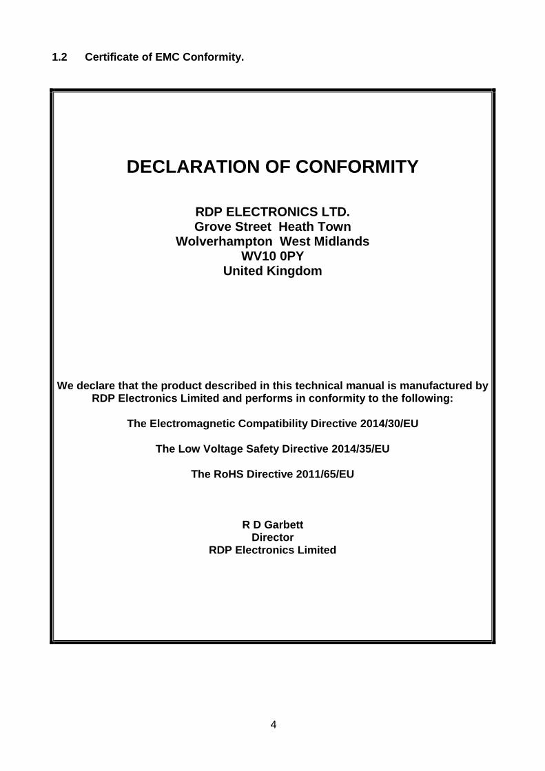
1.2 Certificate of EMC Conformity.
DECLARATION OF CONFORMITY
RDP ELECTRONICS LTD. Grove Street Heath Town
Wolverhampton West Midlands WV10 0PY
United Kingdom
We declare that the product described in this technical manual is manufactured by RDP Electronics Limited and performs in conformity to the following:
The Electromagnetic Compatibility Directive 2014/30/EU
The Low Voltage Safety Directive 2014/35/EU
The RoHS Directive 2011/65/EU
R D Garbett Director
RDP Electronics Limited

5
Fig.1 Connector & Control Locations
Note For mod 12 instruments onwards the frequency resistor is not fitted, different excitation frequencies are available but must be specified at the time of order.
CO
N3
SW
4
F1
CO
N 4
C
ON
1
SW
2
SW
1
CO
N 2
SW
3
LN
E
SU
PP
LY
GA
IN
ZE
RO
RV
1
RV
2
J1
V
I 1 2 3 4 5 6
OP
TIO
N
CO
N6
EX HI EX LO
SIG- SIG+ SCN CAL
ZE
RO
RA
NG
E R
N1
OUT COM
SH.CAL
GA
IN R
AN
GE
SW
6
R17
R10
R
9
BA
L
BA
L R
53
R7
SW
5 CA
L
NORM ZERO OPNZ TEST
Rv5
IN
PU
T
IC1
CO
N5
RL
1
Removable Safety Cover
Supply Fuse
Supply Connections
Supply Selector Switch
Fine Gain & Zero
Option T/E connections
Output (and CAL option Z) connections
Transducer connections
Bridge completion Resistors R7,9,10
Relay (Option Z)
Shunt Cal Switch(Option Z)
Shunt Cal Resistor
Frequency Resistor
Input Signal Selector
Input Amplifier
Balance (Option Z) Switch, Pot
Gain Switch
Bandwidth Change Network
Option T/E Fitting (cons 5&6)
Coarse Zero Switch
Output Voltage/ Current selector

6
2. CONNECTIONS 2.1. Supply
ALWAYS ISOLATE BEFORE ALTERING CONNECTIONS Check that the voltage on the label near the inlet gland is correct for the application. To change the voltage, operate the slide switch so that it indicates 115 or 230 volts to suit the supply. For supplies less than 100V, change solder link SP1 (near the fuse) to B-C). The supply terminal block is revealed on removing the internal clip-on cover (squeeze the tips of the plastic studs to release). The supply lead is fed through the largest of the three glands and is connected as shown below:
L Live 115/230V a.c brown (black US)
N Neutral 0V blue (white US)
E Earth/ground green/yellow (green US)
All metal case parts are connected to the E terminal.
2.2 Input & Output Connections For details of input and output connections, refer to Fig.1 and Fig.2a. To utilise the central gland for both output and option connections, use a multi-core shielded cable such as Farnell 6-core 1A No. 715-244, or RS 9-core 0.25A No. 367-381, or one of the various shielded data cables readily available. 2.3 EMC Compliance 2.3.1 For EMC compliance only shielded multi-core cables should be used for the signal
input and output connections to this instrument. 2.3.2 The shields of the two cables may be connected to the SCN and common terminals
of the transducer connector and output connector, but, for optimum EMC, the cable shield should be terminated as shown in Fig. 2(b).
2.3.3 ESD precautions should be used when working on the instrument with the lid
removed. The user should ensure he is "earthed" by use of an earthed wrist strap or at least touching earth before touching any component, including wires, terminals or switches.
2.3.4 Segregate signal/supply/output cables. 2.3.5 The transducer body should be earthed. Some transducers without an internal
case-to-cable shield connection will require a separate connection. This should be to the instrument cable shield or as near (electrically) as possible to this point.
2.3.6 The supply cable green/yellow wire provides a safety ground but for optimum EMC
it is desirable to bolt the case via the holes provided to a substantial grounded base.
7
Fig.2(a) Examples of connections to various types of transducers Refer to connection diagram supplied with the transducer. 2.4 Connections for LVDT Displacement Transducer (Note 1)
2.5 Connections for Half bridge (Differential Inductance) transducer (Note 1)
Additionally, fit 2 bridge completion resistors: (Note 3) 1) between Excitation + and Signal + 2) between Excitation - and Signal + The resistors should be high stability. For RDP transducers use 1k Ohms
Note 1 The output voltage polarity may be reversed by reversing the excitation connections or, for LVDT, the signal connections.
Note 2 Connect SHIELD as shown in fig. 2b Note 3 Completion resistors may be fitted in positions R7 and R10 (these are
shown in fig.1) or in the transducer connector.
Primary Input 1 (Excitation High)
Primary Input 2 (Excitation Low)
Secondary Output 1 (Signal High)
Secondary Output 2 (Signal Low)
PRIMARY COIL
SECONDARY COIL
Shield (Note 2)
Excitation High
Shield (Note 2)
Excitation Low
Signal -

8
Gland Cap
Plastic Sleeve
Metal Gland Nut
Wall of Instrument Case
Fig.2(b) Signal Cable Installation for Optimum EMC 1
2 Insert the end of the cable, plus the plastic sleeve into the metal outer shell of the gland. The bore of the gland is a tight fit onto the cable shield, giving the required ground contact.
3 Fit gland cap and tighten
Cable Cores Trim Rubber Seal
Cable Shield Double Back Over Plastic Sleeve
Plastic Sleeve Cable
9
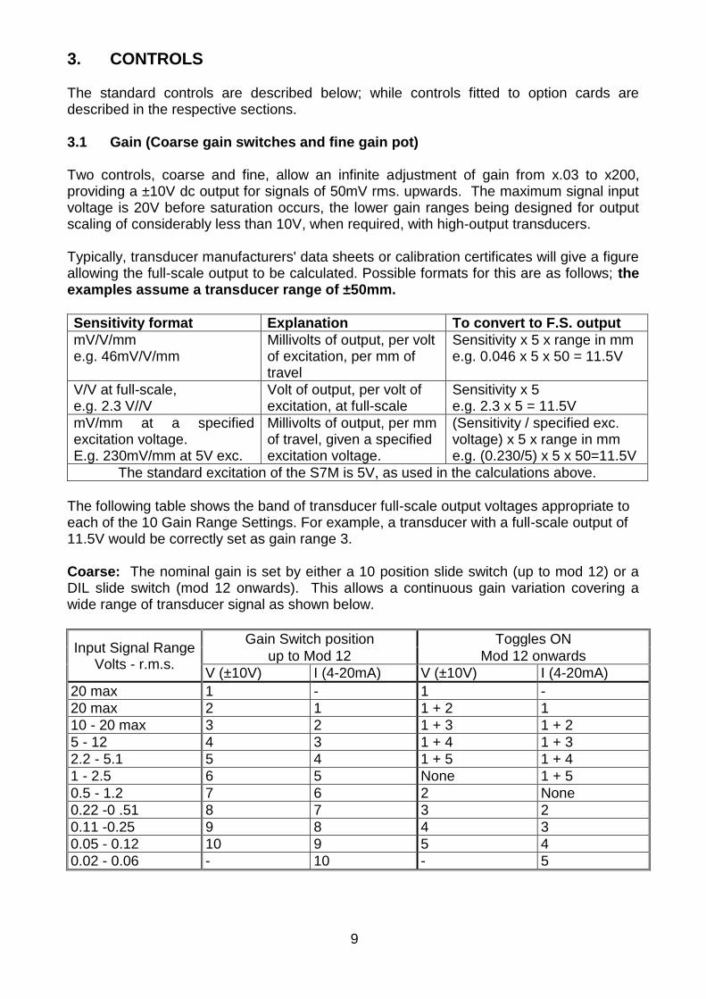
3. CONTROLS The standard controls are described below; while controls fitted to option cards are described in the respective sections. 3.1 Gain (Coarse gain switches and fine gain pot) Two controls, coarse and fine, allow an infinite adjustment of gain from x.03 to x200, providing a ±10V dc output for signals of 50mV rms. upwards. The maximum signal input voltage is 20V before saturation occurs, the lower gain ranges being designed for output scaling of considerably less than 10V, when required, with high-output transducers.
Typically, transducer manufacturers' data sheets or calibration certificates will give a figure allowing the full-scale output to be calculated. Possible formats for this are as follows; the examples assume a transducer range of ±50mm.
Sensitivity format Explanation To convert to F.S. output
mV/V/mm e.g. 46mV/V/mm
Millivolts of output, per volt of excitation, per mm of travel
Sensitivity x 5 x range in mm e.g. 0.046 x 5 x 50 = 11.5V
V/V at full-scale, e.g. 2.3 V//V
Volt of output, per volt of excitation, at full-scale
Sensitivity x 5 e.g. 2.3 x 5 = 11.5V
mV/mm at a specified excitation voltage. E.g. 230mV/mm at 5V exc.
Millivolts of output, per mm of travel, given a specified excitation voltage.
(Sensitivity / specified exc. voltage) x 5 x range in mm e.g. (0.230/5) x 5 x 50=11.5V
The standard excitation of the S7M is 5V, as used in the calculations above.
The following table shows the band of transducer full-scale output voltages appropriate to each of the 10 Gain Range Settings. For example, a transducer with a full-scale output of 11.5V would be correctly set as gain range 3.
Coarse: The nominal gain is set by either a 10 position slide switch (up to mod 12) or a DIL slide switch (mod 12 onwards). This allows a continuous gain variation covering a wide range of transducer signal as shown below.
Input Signal Range Volts - r.m.s.
Gain Switch position Toggles ON
up to Mod 12 Mod 12 onwards
V (±10V) I (4-20mA) V (±10V) I (4-20mA)
20 max 1 - 1 -
20 max 2 1 1 + 2 1
10 - 20 max 3 2 1 + 3 1 + 2
5 - 12 4 3 1 + 4 1 + 3
2.2 - 5.1 5 4 1 + 5 1 + 4
1 - 2.5 6 5 None 1 + 5
0.5 - 1.2 7 6 2 None
0.22 -0 .51 8 7 3 2
0.11 -0.25 9 8 4 3
0.05 - 0.12 10 9 5 4
0.02 - 0.06 - 10 - 5
10
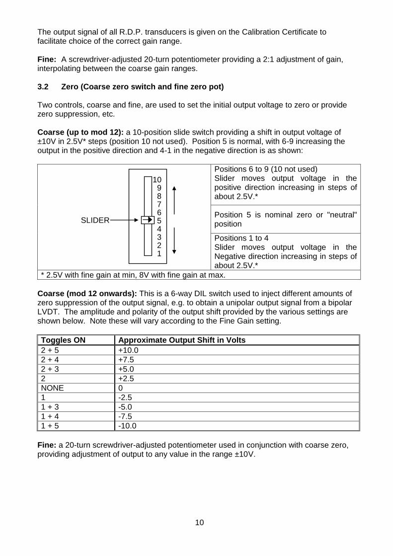
10 9 8 7 6 5 4 3 2 1
SLIDER
The output signal of all R.D.P. transducers is given on the Calibration Certificate to facilitate choice of the correct gain range. Fine: A screwdriver-adjusted 20-turn potentiometer providing a 2:1 adjustment of gain, interpolating between the coarse gain ranges. 3.2 Zero (Coarse zero switch and fine zero pot) Two controls, coarse and fine, are used to set the initial output voltage to zero or provide zero suppression, etc. Coarse (up to mod 12): a 10-position slide switch providing a shift in output voltage of ±10V in 2.5V* steps (position 10 not used). Position 5 is normal, with 6-9 increasing the output in the positive direction and 4-1 in the negative direction is as shown:
Positions 6 to 9 (10 not used) Slider moves output voltage in the positive direction increasing in steps of about 2.5V.*
Position 5 is nominal zero or "neutral" position
Positions 1 to 4 Slider moves output voltage in the Negative direction increasing in steps of about 2.5V.*
* 2.5V with fine gain at min, 8V with fine gain at max.
Coarse (mod 12 onwards): This is a 6-way DIL switch used to inject different amounts of zero suppression of the output signal, e.g. to obtain a unipolar output signal from a bipolar LVDT. The amplitude and polarity of the output shift provided by the various settings are shown below. Note these will vary according to the Fine Gain setting.
Toggles ON Approximate Output Shift in Volts
2 + 5 +10.0
2 + 4 +7.5
2 + 3 +5.0
2 +2.5
NONE 0
1 -2.5
1 + 3 -5.0
1 + 4 -7.5
1 + 5 -10.0
Fine: a 20-turn screwdriver-adjusted potentiometer used in conjunction with coarse zero, providing adjustment of output to any value in the range ±10V.
11
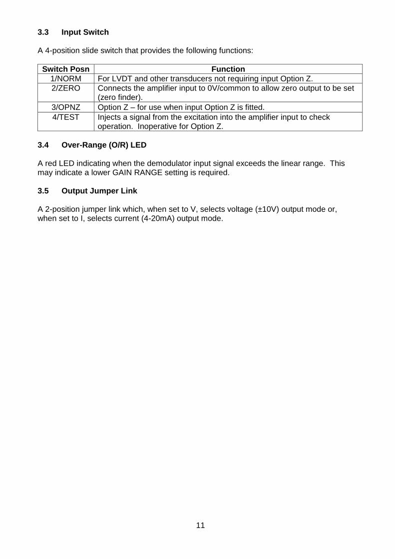
3.3 Input Switch A 4-position slide switch that provides the following functions:
Switch Posn Function
1/NORM For LVDT and other transducers not requiring input Option Z.
2/ZERO
Connects the amplifier input to 0V/common to allow zero output to be set (zero finder).
3/OPNZ Option Z – for use when input Option Z is fitted.
4/TEST
Injects a signal from the excitation into the amplifier input to check operation. Inoperative for Option Z.
3.4 Over-Range (O/R) LED
A red LED indicating when the demodulator input signal exceeds the linear range. This may indicate a lower GAIN RANGE setting is required. 3.5 Output Jumper Link
A 2-position jumper link which, when set to V, selects voltage (±10V) output mode or, when set to I, selects current (4-20mA) output mode.

12
4. SETTING-UP PROCEDURES 4.1 Voltage Output - LVDT & Half bridge (differential inductance) Transducer 4.1.1 Determine the transducer output from the manufacturer's data and set the coarse
gain. Refer to section 3.1. 4.1.2 Connect the transducer to the 6-way connector as detailed in Figure 2. Switch ON
power and allow a 20-minute warm-up period (for maximum accuracy). 4.1.3 Set the INPUT Switch to ZERO and adjust the ZERO controls for zero output
(measured with a voltmeter). 4.1.4 Set the INPUT switch to NORM (normal). Adjust the transducer armature until the
output is zero volts (measured with a voltmeter). (The FINE ZERO control may be used to obtain an absolute zero indication if the armature adjustment is too coarse.) This determines the transducer centre-stroke position.
Now proceed with either 4.15 or 4.16 according to application.
4.1.5 Bipolar Operation, e.g. ±5mm gives ± 10V output. (a) Move the transducer armature by a precise amount, usually the full scale. (E.g.
5mm (0.200 inches) for ±5mm (±0.2") transducer) and adjust the FINE GAIN control for the desired output, e.g. 10V. If the output polarity is wrong, reverse the signal wires (blue/green).
(b) Relocate the transducer armature at the centre of the stroke and check that the
OUTPUT is zero, re-adjust the FINE zero control if necessary. Repeat (a). (c) Move the armature 5mm (0.2 inches) the other side of centre-stroke and check for -
10V. (A small discrepancy is allowed) 4.1.6 Unipolar Operation, e.g. 0 - 10mm stroke gives 0-10V output. In order to obtain a 0 to 10V output for ± Full scale on the transducer, first calibrate the transducer for ±5V for ± Full scale as detailed in 4.15 Position the transducer such that the output is 0V. Using the coarse and fine ZERO controls offset the output by +5V. This adds 5V to all positions so that -5V becomes 0V and +5V becomes 10V. 4.2 4-20mA Output - LVDT & Half bridge (differential inductance) Transducer Full stroke operation, e.g. ±5mm (10mm) stroke gives 4-20mA output. 4.2.1 Determine the transducer output from the manufacturer's data sheet and set the
coarse gain control. (Refer to section 3.1). 4.2.2 Connect the transducer to the 6-way connector as detailed in figure 2. Change
jumper link J1 to position "I". Switch ON power and allow a 20-minute warm-up period (for maximum accuracy).

13
4.2.3 Set the INPUT switch to ZERO and adjust the ZERO controls for 4mA output.
(Measured with an ammeter) 4.2.4 Set the INPUT switch to NORM (normal). Adjust the transducer armature until the
output is 4mA (measured with a current meter). (The FINE ZERO control may be used to obtain an absolute 4mA indication if the armature adjustment is too coarse.) This determines the transducer centre-stroke position.
4.2.5 Move the transducer armature to the positive full scale position e.g. +5mm (+0.2 ")
for a ±5mm (±0.2") transducer and adjust Fine Gain for 12mA output. 4.2.6 Move the transducer armature to the centre-stroke position and adjust FINE ZERO
for 4mA output if necessary. 4.2.7 Repeat 4.25 and 4.26 until consistent results are achieved. (This may take a
number of settings due to the interaction of the controls.) 4.2.8 Move the transducer armature to the negative full-scale position and use the
COARSE and FINE ZERO controls to set 4mA output. 4.2.9 Move the armature to the positive full-scale position and check output is 20mA.
Repeat 4.28 and 4.29 if necessary.

14
5. LIMITS OPTION T This is a plug-in module with two separate trip limit circuits. Refer to section 5.5 for details of specification. Each limit may be configured as a high or low (positive- or negative-going) detector with normally open/closed relay outputs. The relays may be operated in normally energised (fail-safe) or de-energised modes. Limit status is indicated by two LEDs, which are ON when the relay is energised, irrespective of operating mode. Limit levels are set via multi-turn potentiometers over the range ±10v and monitored via two test points, TP1 (L1) and TP2 (L2). 5.1 Setting the Limit Levels (see also section 5.4) The limit levels may be set in two ways: - (a) Monitoring the potentiometer levels at test point TP1 (L1) or TP2 (L2) with a
voltmeter with respect to common TP3 (0V). The meter impedance should be >1MΩ.
(b) Adjust the transducer for the required output signal level then adjust the limit potentiometer until the LED changes state.
5.2 Connections
Connections to the limits relays are made via the 6-way terminal block labelled "OPTION" as follows:-
Function Terminal
1 NO 1
1 Common 2
1 NC 3
2 NO 4
2 Common 5
2 NC 6
5.3 Controls (for location, refer to Fig.3) 5.3.1 Polarity Switches (SW1, 2) These are 2-position slide switches that determine whether the limits are high (positive going) or low (negative going). Set in the UP position for high and DOWN for low. Refer also to Table 1. 5.3.2 Relay Mode Switches (SW3, 4) These two switches, similar to the polarity switches, are used to determine whether the relays are in a normally energised or normally de-energised mode. For normally de-energised, set the switches in the UP position; and for normally energised (e.g. fail-safe mode), set the switches in the DOWN position. Refer also to Table 1 for more details.
15
RV2
LED2
TP2
SW4 SW2
Set Level
LED
Test Point
Mode Switch
Polarity Switch
LIMIT 2
RV1
LED1
TP1
SW3 SW1
Set Level
LED
Test Point
Mode Switch
Polarity Switch
LIMIT 2
Fig.3 Limits Option control Locations
TABLE 1 RELAY OUTPUT OPERATION Note 1: A HIGH limit monitors positive-going signals.
A LOW limit monitors negative-going signals < Means more negative than: > means more positive than. N means normal (as despatched) settings
Note 2: In fail safe mode the relay is OFF (de-energised) when limit is exceeded or power is removed.
Limit Type POL.
SW 1,2 MODE SW
3,4 SIGNAL wrt LIMIT LED/ RELAY COMMENTS
1.HIGH UP (N) UP (N) < >
OFF ON
2.HIGH UP DOWN < >
ON OFF
FAIL SAFE
3.LOW DOWN UP < >
ON OFF
4.LOW DOWN DOWN < >
OFF ON
FAIL SAFE
5.4 Limits Operation with 4-20mA Output When using current (4-20mA) output mode, the signal applied to the limits option board is derived from the output of a current-sensing amplifier which acts as a current to voltage converter. The limit level voltages, as monitored via the L1, L2 test points, are compared to this current-derived signal and should be set with reference to the formula: Limit level voltage = output current in mA x 0.25 volts. E.g. for 20mA output, the voltage applied to the limit is 20 x 0.25 = 5V. So, for a limit to operate at 20mA output set the test point level to 5V.

16
5.5 Limits Option Specification
Channels 2 independent
Signal Range ±10V/±20mA (see Section 5.4)
Accuracy ±10mV typical (0.05% FS) (With signal noise <1mV)
Response Speed 6ms
Tempco 0.1mV/°C (0.0005% FS) typical
Outputs Normally open or closed (selectable) 1A, 30Vdc/0.5A, 125Vac
Hysteresis 20mV typical
Expected life cycle 5 x 10⁶ operations
6. OPTION E MAX/MIN STORE This optional circuit board provides a separate output signal that may be selected (via an external wire link) to store either the maximum/ peak or minimum/trough value of the normal output signal (which remains unaffected at the normal output terminal). The circuit combines high speed and accuracy with zero output droop. Note that MAXIMUM = the most positive value, and MINIMUM = the most negative value of the output signal range.
6.1 Connections Terminal Function
These are made via the 6-way terminal block labelled OPTION as follows: The stored (peak or trough) output is monitored via terminals 1 and 2. Terminal 2 is internally connected to the normal output common.
1 Store output (±10V)
2 Output common (0V)
3 +15V output (see text)
4 Reset input : isolated
5 Reset common : isolated
6 Max/Min select
The reset input is opto-isolated to improve EMC. To utilise this facility fully, an external supply should be connected between terminals 4 and 5 to reset the output, then disconnected prior to beginning a new measurement. If an external supply is not available, the S7M +15V output may be used, which removes the benefits of isolation. Connecting terminal 3 (15V) to 4, and 5 to 2 common (via switch etc.) will reset the output. With no connection to terminal 6, the unit will operate in peak store mode (determined via an internal pull-up resistor). To operate in trough mode, connect 6 to 2. 6.2 Specification
Signal Range ±10V
Accuracy ±0.1% FS. (±20mV plus any signal ripple. See note.)
Response Speed 0 – FS (10V) in 1ms for 0.1% accuracy
Reset input Opto-isolated 5 to 24V into 2.2k + diode for 50ms. Isolation 240V.
Max/Min Select Link to unit common (0V) or TTL low (internal 10k pull-up)
Output ±10V at 5mA
Note: The Option E board contains an extra active filter circuit to reduce the errors attributable to carrier ripple.
17
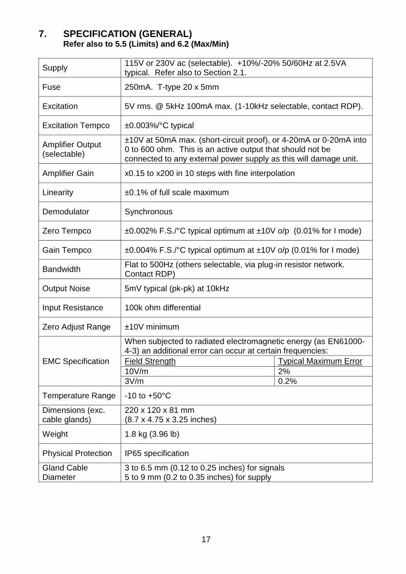
7. SPECIFICATION (GENERAL) Refer also to 5.5 (Limits) and 6.2 (Max/Min)
Supply 115V or 230V ac (selectable). +10%/-20% 50/60Hz at 2.5VA typical. Refer also to Section 2.1.
Fuse 250mA. T-type 20 x 5mm
Excitation 5V rms. @ 5kHz 100mA max. (1-10kHz selectable, contact RDP).
Excitation Tempco ±0.003%/°C typical
Amplifier Output (selectable)
±10V at 50mA max. (short-circuit proof), or 4-20mA or 0-20mA into 0 to 600 ohm. This is an active output that should not be connected to any external power supply as this will damage unit.
Amplifier Gain x0.15 to x200 in 10 steps with fine interpolation
Linearity ±0.1% of full scale maximum
Demodulator Synchronous
Zero Tempco ±0.002% F.S./°C typical optimum at ±10V o/p (0.01% for I mode)
Gain Tempco ±0.004% F.S./°C typical optimum at ±10V o/p (0.01% for I mode)
Bandwidth Flat to 500Hz (others selectable, via plug-in resistor network. Contact RDP)
Output Noise 5mV typical (pk-pk) at 10kHz
Input Resistance 100k ohm differential
Zero Adjust Range ±10V minimum
EMC Specification
When subjected to radiated electromagnetic energy (as EN61000-4-3) an additional error can occur at certain frequencies:
Field Strength Typical Maximum Error
10V/m 2%
3V/m 0.2%
Temperature Range -10 to +50°C
Dimensions (exc. cable glands)
220 x 120 x 81 mm (8.7 x 4.75 x 3.25 inches)
Weight 1.8 kg (3.96 lb)
Physical Protection IP65 specification
Gland Cable Diameter
3 to 6.5 mm (0.12 to 0.25 inches) for signals 5 to 9 mm (0.2 to 0.35 inches) for supply

18
8 APPLICATION NOTES & APPENDICES 8.1 App. Note 2 Electrical Interference Problems When a Transducer Amplifier is used in an industrial application, some of the following points may be helpful to system engineers to design a trouble-free installation. In general the operation of electronic instruments and transducers can be affected by electrical interference. This interference can be generated by the switching of large or reactive loads on the supply causing the production of large voltage spikes and/or variation in the ac mains supply. Higher frequency interference (radio frequency) is often generated by a large voltage (e.g. back emf from a coil) being switched by a contact. Generally a contact seen to arc whilst switching is producing RF interference. Other sources of RF include portable radios, telephones, etc. The interference "signals" can enter a transducer measuring system in the following ways:
a) Direct pick-up by wiring to the instrument. The wiring can be a connection to the transducer supply input or control (e.g. trip relay).
b) Direct pick-up into the instrument. c) Along the mains supply lines.
There are two methods of countering these problems: a) Suppress the interference generation at source. b) Prevent the interference gaining access to the instrumentation circuitry.
Suppression at source is often the best approach. AC coils can often effectively be suppressed by means of connecting, as close to the coil terminals as possible, a 100 Ohm resistor in series with 0.1μF across the coil. Proprietary transient voltage clippers - either non-linear resistor or better semiconductor types - are very useful for suppression, mounted across coils and contacts. Although RDP instruments are fitted with supply suppressors, an exceptionally noisy mains supply can be improved by means of a mains filter unit. These units in their simplest form consist of capacitors and inductors. Mounted at the point where the mains enters the instrument, they can be most effective. A constant voltage transformer is another effective way of cleaning up the mains. Extra shielding of the transducer, cabling and instrument is a simple, low cost method of preventing particularly directed radiated RF type of interference. Shielded cable should always be used to connect the transducer to the instrument. Shielded cable is often beneficial for other connections as well. The shield should only be earthed at the instrument end. It is not good practice to mount the instrument near to contactors, motors, switch transformers, solenoids, etc., but where it is considered necessary to mount the instrument near to such devices, an extra steel enclosure around the instrument would be essential.
19
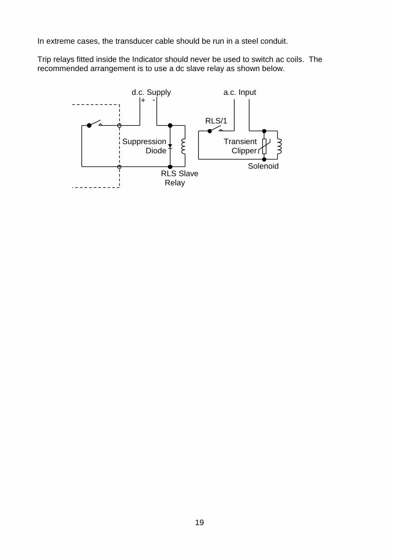
Suppression Diode
Transient Clipper
RLS Slave Relay
Solenoid
RLS/1
d.c. Supply + -
a.c. Input
In extreme cases, the transducer cable should be run in a steel conduit. Trip relays fitted inside the Indicator should never be used to switch ac coils. The recommended arrangement is to use a dc slave relay as shown below.
20
9 WARRANTY AND SERVICE
WARRANTY. R.D.P. Electronics products are warranted against defects in materials or workmanship. This warranty applies for one year from the date of delivery. We will repair or replace products that prove to be defective during the warranty period provided they are returned to R.D.P. Electronics. This warranty is in lieu of all other warranties, expressed or implied, including the implied warranty of fitness for a particular purpose to the original purchaser or to any other person. R.D.P. Electronics shall not be liable for consequential damages of any kind. If the instrument is to be returned to R.D.P. Electronics for repair under warranty, it is essential that the type and serial number be quoted, together with full details of any fault. SERVICE. We maintain comprehensive after-sales facilities and the instrument can, if necessary be returned to our factory for servicing. Equipment returned to us for servicing, other than under warranty, must be accompanied by an official order as all repairs and investigations are subject to at least the minimum charge prevailing at the date of return. The type and serial number of the instrument should always be quoted, together with full details of any fault and services required. IMPORTANT NOTES. 1. No service work should be undertaken by the customer while the unit is under
warranty except with the authorisation of RDP Electronics. 2. If the instrument is to be returned to R.D.P. Electronics for repair, (including
repair under warranty) it is essential that it is suitably packed and that carriage is insured and prepaid. R.D.P. Electronics can accept no liability whatsoever for damage sustained during transit.
3. It is regretted that the above warranty only covers repairs carried out at our factory. Should the instrument have been incorporated into other equipment that requires our engineers to perform the repair on site, a charge will be made for the engineer's time to and from the site, plus any expenses incurred
The aforementioned provisions do not extend the original warranty period of any product that has been either repaired or replaced by R.D.P. Electronics.
THIS WARRANTY MAY BE NULL AND VOID SHOULD THE CUSTOMER FAIL TO MEET OUR TERMS OF PAYMENT.