technical report for the design, construction and ... · group leader in matters of safety ... pcb...
TRANSCRIPT
Technical Report For the Design, Construction andCommissioning of the Advanced Implantation Detector
Array (AIDA)
November 2008
Abstract
The Advanced Implantation Detector Array project is a silicon detector array designed forimplantation-decay correlation measurements for exotic nuclei produced by the SuperFRS.The project has been fully funded by the UK. Specification has been completed and detaileddesign is underway. Prototype hardware will be available for test in 2009.
1
1 AIDA Collaboration
School of Physics & Astronomy, University of Edinburgh, Edinburgh, UKProfessor P.J.Woods, T.Davinson, Z.Liu, A.St.J.Murphy
Department of Physics, University of Liverpool, Liverpool, UKProfessor R.D.Page, Professor P.J.Nolan, S.Rinta-Antila, D.Seddon
STFC Daresbury and Rutherford Appleton Laboratories, UKProfessor J.Simpson, D.Braga, P.J.Coleman-Smith, I.Lazarus, S.Letts, M.Prydderch,V.F.E.Pucknell, J.Strachan, S.L.Thomas
Spokespersons: Professor P.J.Woods, Professor R.D.Page, Professor J.Simpson
Project Manager: T.Davinson
Group Leader in Matters of Safety (GLIMOS): T.Davinson
2

2 Introduction and overview
The objective of the Advanced Implantation Detector Array (AIDA) project is to develop,commission and exploit a state of the art silicon detector array for decay spectroscopyexperiments using the SuperFRS fragment separator at FAIR. It is anticipated that AIDAwill be operated standalone and in conjunction with other DESPEC collaboration detectionsystems, such as gamma-ray and neutron detector arrays, which requires that AIDA shouldbe very compact and use minimum material while still accepting all ions from the fragmentseparator.
To achieve these objectives AIDA will use large area double-sided silicon strip detector(DSSSD) and application specific integrated circuit (ASIC) technologies. AIDA will beused for implantation-decay experiments and perform spectroscopy quality measurementsof charged particle decays with energies from tens of keV to MeV. The challenge is toachieve this within microseconds of multi-GeV exotic ion implants and with an instrumen-tation density to match the very high degree of detector segmentation required for theobservation and characterisation of long-lived decays.
This project is fully funded by the UK Science & Technology Facilities Council (STFC)by grants to each of the AIDA collaborators. The project commenced August 2006 andprototype detectors and instrumentation will be available for in-beam tests in 2009, to befollowed by production detectors and instrumentation in 2010.
3 Physics requirements for subsystem
3.1 Implantation-Decay Correlation
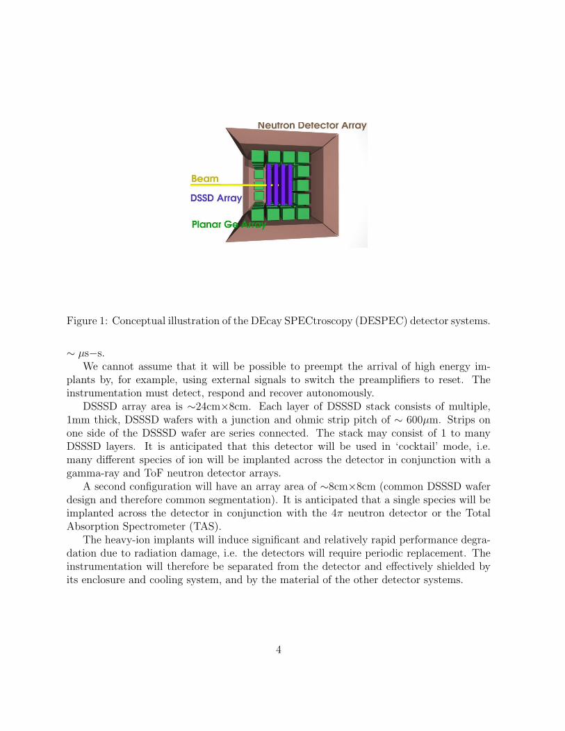
Very high energy (∼ 100−200MeV/u, A ≤ 240 ions), very exotic heavy-ions are implantedinto a stack of double-sided silicon strip detectors (DSSSDs). These nuclei subsequentlyundergo radioactive decay emitting low energy β-particles, protons, α-particles, neutronsand γ rays. The charged particles are detected by the DSSSDs. The detector systems areschematically illustrated in figure 1
The DSSSD strips identify where (x, y) and when (t0) the nuclei were implanted. Subse-quent radioactive decay(s) at the same position (x, y) at times t1(, t2 ... ) can be correlatedwith the implant. Observation of a number of such correlations enables the determinationof the energy distribution of the radioactive decay and its half-life.
If the implantation events are distributed across a highly segmented DSSSD the averagetime between implants at each position (x, y) is greater than the average decay time andrandom correlations are minimised. For a given decay time, higher segmentation means ahigher total implantation rate.
3.2 Practicalities
The energy deposited by the implant in the DSSSD is ∼GeV, and higher. The energy ofthe subsequent decay events is ∼MeV. Average time between implantation and decay is
3
2
Figure 1: Conceptual illustration of the DEcay SPECtroscopy (DESPEC) detector systems.
∼ µs−s.We cannot assume that it will be possible to preempt the arrival of high energy im-
plants by, for example, using external signals to switch the preamplifiers to reset. Theinstrumentation must detect, respond and recover autonomously.
DSSSD array area is ∼24cm×8cm. Each layer of DSSSD stack consists of multiple,1mm thick, DSSSD wafers with a junction and ohmic strip pitch of ∼ 600µm. Strips onone side of the DSSSD wafer are series connected. The stack may consist of 1 to manyDSSSD layers. It is anticipated that this detector will be used in ‘cocktail’ mode, i.e.many different species of ion will be implanted across the detector in conjunction with agamma-ray and ToF neutron detector arrays.
A second configuration will have an array area of ∼8cm×8cm (common DSSSD waferdesign and therefore common segmentation). It is anticipated that a single species will beimplanted across the detector in conjunction with the 4π neutron detector or the TotalAbsorption Spectrometer (TAS).
The heavy-ion implants will induce significant and relatively rapid performance degra-dation due to radiation damage, i.e. the detectors will require periodic replacement. Theinstrumentation will therefore be separated from the detector and effectively shielded byits enclosure and cooling system, and by the material of the other detector systems.
4
3.3 Required Capabilities
• Selectable Gainhigh ∼20MeV Full Scale Range (FSR) OR intermediate ∼1GeV FSR
AND
low ∼20GeV FSR (via separate overload recovery signal processing)energy measurement of implantation and decay events
• Selectable threshold < 0.25 − 10% FSR Minimum threshold <50keV @ high gain⇒ rms noise <5keV assuming threshold = 5σobserve and measure low energy betas, beta detection efficiency
• Integral < 0.1% and differential non-linearity < 2% for > 95% FSRspectrum analysis, calibration, threshold determination
• Autonomous overload detection and recovery ∼ µsobserve and measure fast implantation-decay correlations
• Nominal signal processing time < 10µsobserve and measure fast decay-decay correlations
• Receive(transmit) time-stamp datacorrelate events with data from the DAQs of other detector sub-systems (gamma andneutron detector arrays, upstream tracking detectors)
• Timing trigger for coincidences with other detector systemstime resolution < BUTIS clock period (5ns)minimise random correlations, DAQ rate management, neutron ToF
4 Technical specification and design details
4.1 Double Sided Silicon Strip Detector (DSSSD)
4.1.1 DSSSD Wafer
• DC design
• Common biasing to p+n junction and n+n ohmic strips via integrated polysiliconresistors (15 ± 5)MΩ
• Detector thickness 1000µm
• 8cm × 4cm (4′′ wafer technology)
• 128 × 64 strips (8cm × 4cm)
5

• Strip pitch ∼ 600µm
• Inter-strip distance 50µm (consistent with obtaining > 107MΩ resistance betweenn+n ohmic strips)⇒∼ 85% of detector area is active
• Multiple guard rings for both p+n junction and n+n ohmic sides of the wafer
• Dead space (passivation, guard rings, common bias line and polysilicon bias resistors)surrounding active area ≤ 1.5mm
• Operating bias ≤ 200V
• Typical wafer leakage current 1−5nA/cm2/100µm (20C) at operating bias ⇒ 0.64−3.2µA for 8cm × 8cm area and 1000µm thickness
• Maximum (8cm × 8cm) wafer leakage current < 5µA (20C) at operating bias
• Maximum strip leakage current < 100nA (20C) at operating bias
• 100% of strips functional to above specification
Operating bias is defined as the voltage required to obtain maximum charge collectionand equivalent resolution for p+n junction and n+n ohmic strips for α-particles, whetherincident on the junction or ohmic strips.
4.1.2 DSSSD Package
• Two package types: (i) 24cm × 8cm using (6 off 4cm × 8cm wafers) with seriesbonded n+n strips, (ii) 8cm × 8cm using (2 off 4cm × 8cm wafers) with seriesbonded n+n strips
• FR4 transmission PCB mounting
• Flexible Kapton PCB cabling directly bonded to PCB
• Tri-plate (ground/signal/ground planes) flexible Kapton PCB
• Flexible Kapton PCB length ∼60cm
• PCB design to permit (i) use at any position in DSSSD stack, (ii) use at 0 or 180
with respect to an axis normal to the surface of the detector and other DSSSD planesin the stack
• PCB design to include thermocouple connection point
• PCB dimensions ∼ 26cm × 10cm ×3mm, ∼ 10cm × 10cm ×3mm,
6

4.1.3 Planned DSSSD Procurement
• 1 off prototype 24cm × 8cm detector
• 1 off prototype 8cm × 8cm detector
• 9 off production 24cm × 8cm detectors
• 9 off production 8cm × 8cm detectors
4.2 Intrinsic Resolution Limits of Silicon Detectors
The term intrinsic detector resolution refers to the response of a detector to a mono-energetic source of radiation and assumes that we can neglect the effects of dead layer,recombination, trapping and incomplete charge collection.
For β-particles we assume that the energy resolution will be equivalent to the electronicnoise of the instrumentation. For protons and α-particles we assume that the energy resolu-tion will be the quadratic sum of the statistics of the ionisation process, the effects of nuclearcollisions at the end of the particle track and the electronic noise. Statistics: for 1MeVprotons and 5MeV α-particles the contributions are 1.5keV FWHM and 3.4keV FWHMrespectively. Collisions: for protons and α-particles the contributions are 0.7keV FWHMand 6.3keV FWHM respectively. For 1MeV protons and 5MeV α-particles the quadraticsums of the statistical and collisional contributions are 2.3keV FWHM and 7.2keV FWHMrespectively. Unless the electronic noise is significantly lower than 12keV FWHM (1400e−
rms), the intrinsic detector resolution will be dominated by the electronic noise. If weassume (i) a resolution of 12keV FWHM, (ii) that data from discrete (Gaussian) peaksshould be spread over 4 channels FWHM (for accurate centroid determination) and (iii)that the high gain range corresponds to 20MeV FSR then this implies 13-bit ADCs.
For heavy-ions (A ≥ 12) the intrinsic energy resolution will be completely dominatedby the effects of nuclear collisions at the end of the particle track and charge collectioneffects arising from the high density charge deposition. Lindhard and Neilson (Phys. Lett.2 (1962) 209) estimate the contribution from nuclear collisions as
∆Ecoll(keV FWHM) = 0.7Z1
2 A4
3 (1)
which ranges in value from ∼0.8MeV (58Ni) to ∼10MeV (238U).
7

4.3 Implantation Event Characteristics
The maximum energy loss of heavy-ions in 1mm of silicon (normal incidence):
∆Emax
Ion (GeV)58Ni 3
120Sn 7238U 17
The maximum energy that can be deposited in 1mm of silicon at, or near, normal incidenceis therefore ≤20GeV which establishes the FSR requirement for the high-energy signalprocessing instrumentation.
Range of heavy-ions in silicon as a function of incident energy (normal incidence):Range (mm)
Ion 50MeV/u 100MeV/u 200MeV/u 300MeV/u58Ni 1.0 3.3 11.8 20.9
120Sn 0.8 2.3 7.1 13.7238U 0.6 1.7 4.7 8.9
Calculations performed using SRIM-2003 (http://srim.org). To implant ions at a distanceof 3 − 5mm into the DSSSD stack requires energies of ∼ 100 − 200MeV/u.
Multi-GeV implants are expected to result in data from a cluster of strips for eachDSSSD plane traversed by the ion. It is expected that ∼5 adjacent p+n junction and ∼5adjacent n+n ohmic strips per DSSSD plane will produce data per event with the majorityof the energy to be found at the cluster centre.
The energy and spatial distribution for the incoming implantation ions will be deter-mined by the properties of the SuperFRS, low-energy branch (LEB) and any degraders,tracking detectors, AIDA entrance window etc. We assume that ions of a given A/q willbe implanted across the DSSSD planes with a Gaussian transverse profile (σx = σy ∼ 1cm)and a depth distribution (σz ∼ 1− 2mm). We assume implantation rates across the 24cm× 8cm DSSSD plane of ∼ 10kHz, with peak rates for ions with a given A/q ∼ 1kHz. If wewish to observe lifetimes ∼s then this implies a segmentation of ∼ 0.5mm × 0.5mm.
The observables of interest are:
• position/track of implantp+n and n+n strip numbers
• absolute energy of implantto ∼ 0.1% precision
8

• implant timefor time correlation with respect to (i) subsequent charged-particle decay events and(ii) isomeric decays detected by other detector arrays, precision (per event) 5ns
• time of implantby prompt trigger, precision < 5ns
4.4 Decay Event Characteristics
Typical decay event for protons (energy 0.5 − 2MeV, range 7 − 50µm) and α-particles(energy 3 − 12MeV, range 15 − 100µm) will consist of one p+n junction strip and onen+n ohmic strip from one DSSSD plane. A fraction of events (inter-strip area:total area)will occur between strips and these events will typically be 1 or 2 adjacent p+n junctionstrip(s) and 1 or 2 adjacent n+n ohmic strip(s). In addition, for those decays due toimplants close (< 100µm) to the surfaces of the DSSSDs it is possible for the decay to havesufficient energy to escape one DSSSD plane and be stopped in another. These eventswould therefore consist of data from two DSSSD planes with the event structure for eachDSSSD plane as described above.
β-particles of interest will have energies in the range from ∼tens of keV to > 10MeV(range >25mm) - a large fraction of the β-particles of interest will not be stopped in oneDSSSD plane. In addition, there is a significant probability that the β-particles will bescattered by the silicon. Events can therefore consist of data from multiple adjacent stripsand DSSSD planes. There will be inter-strip events as described above.
The observables of interest are:
• position of decayp+n and n+n strip numbers
• absolute energy of charged-particle decaycentroid of energy distribution of multiple decays to 1LSB
• absolute energy of thresholdβ detection efficiency, to 1LSB
• decay timefor time correlation with respect to previous implantation events or charged-particledecays, precision (per event) 5ns
• time of decayby prompt trigger for time of flight (ToF) measurements, precision < 5ns
4.5 Radiation Damage
The MSL type BB/5 DSSSD (area 32mm × 32mm, thickness ∼ 70µm) is used for im-plantation decay experiments using the Fragment Mass Analyser (FMA) at the Argonne
9

National Laboratory. These detectors continue to provide useful data with leakage currents≤ 5µA at ∼ −10C. Scaling by area and thickness to the AIDA DSSSD we could expecta leakage current of ∼ 450µA per 8cm × 8cm wafer or ∼ 3µA per strip at ∼ 0C. Thisper strip leakage current would correspond to ∼50keV FWHM of noise for a shaping timeτ = 1µs: the noise would vary as
√τ (see Appendix A). This might be sufficient for some
measurements of α and proton decays but it would compromise low threshold detection ofβ-particles as the threshold would need to be increased to ∼110keV (5σ).
The above considerations indicate that it would be advantageous to cool the DSSSDsto a temperature significantly below 0C. Because the silicon wafers are attached to thedetector PCB using an electrically conductive epoxy the lower temperature limit is ∼−20C. The DSSSDs and their mounting will need to be designed to ensure good thermalcontact to achieve and maintain the temperatures required. Thermocouples to measurethe temperature of the mounting and DSSSD PCB temperature will also be required.
Caveats The MSL type BB/5 is used with 40− 80MeV A = 100− 200 ions which havea range significantly less than the thickness of the silicon wafer - damage is localised indepth (whereas for AIDA DSSSDs it will be more uniformly distributed through the waferthickness) and therefore the scaling probably underestimates the leakage current of theAIDA detector. The MSL type BB/5 detector bias is usually set at ×3 − 5 the depletionvoltage - this is significantly higher than we will be able to achieve with the AIDA DSSSD,therefore the scaling probably overestimates the leakage current of the AIDA detector.This might also indicate that we will not be able to achieve equivalent charge collectionand therefore resolution with the lower electric field of the 1000µm AIDA DSSSDs andtherefore not be able to operate at equivalent levels of radiation damage.
4.5.1 Mitigation strategies
• Rotate detector layers - distribute radiation dose
• Detector cooling - leakage current reduction, improved charge collection
• Increased detector bias - improved charge collection
• Instrumentation physically separated from DSSSDs
4.6 Application Specific Integrated Circuit (ASIC)
A schematic diagram of ASIC functionality is shown in figure 2.
4.6.1 Low-energy channel (0 − 20MeV)
Preamplifier
• Differential input, with adjustable operating point, for optimum performance for bothpolarities of charge
10

• Feedback capacitor ∼ 1pF, with feedback stabilisation circuit (equivalent to a high-value resistor)
• Input referred noise 1400e− rms = 12keV FWHM (Si), preferably lower
• Adjustable operating point, for optimum performance with both positive and nega-tive charge
• Integral non-linearity < 0.1%.
Shaper
• Variable shaping time (∼ 0.5 − 5µs), to minimise ballistic deficitRisetime variations < 0.05τ to maintain ballistic deficit effects < 0.1% assumingCR − RC shaping (K.Hatch, IEEE Trans. Nucl. Sci. NS15 (1968) 303).
• ∼ 1V range of output voltage
• Integral non-linearity < 0.1%
Slow amplifier/comparator
• Bandwidths matched to shaper (to avoid adding noise)
• Amplifier with ×10 gain before comparator, to minimise effect of offset variations
• Usable threshold range 50keV−2MeV (0.25 − 10% full-scale)
• Low end of threshold determined by offsets and noise - desirable to achieve 25keV
Fast comparator
• Signal taken straight from pre-amp output, without band-limiting
• Timing resolution <5ns, but with high noise (unsuitable for operation with lowthresholds)
• Direct connection to control logic, to provide high-speed digital timing pulseshould be OR’d with slow comparator output
Peak-hold
• Rectifying current mirror architecture (to maintain output linearity)
• Low-leakage design, for good stabilityAssume 1V FSR, 14-bit ADC ⇒ 1LSB = 61µVDroop 1LSB, 0.1LSB say ⇒ droop < 6µV per readout cycle (< 10µs)
11

Control
Peak
Preamp
Shaper
Disc
Fast
Fast
Disc
SlowDisc
SlowAmp
Hold
ControlLogic
Logic
MUX
MUX
Shaper
AnalogueInput
PeakHold
DigitalOutput
AnalogueOutput
Digital
AnalogueOutput
Output
CM
OS
Sw
itche
s
Preamp
Low & Intermediate Energy Range
High Energy Range
SamplingADC
SamplingADC
Figure 2: Schematic diagram of the functionality of one ASIC channel
4.6.2 Intermediate energy channel (0 − 1GeV)
Preamplifier feedback ∼ 50pF. Scale noise, minimum threshold etc. from low energy(0 − 20MeV) specification.
4.6.3 High-energy channel (0 − 20GeV)
Pre-amp
• Similar to low-energy design, but optimised for ∼ 1nF feedback capacitor
• Large current flow in amplifier output transistors (needs to exceed the peak currentfrom the detector)
• Input referred noise ∼ 5 × 10⁶e−rms, ∼50MeV FWHM (Si).
Diode and CMOS switches
• Diode to connect high-energy amplifier to detector when low-energy channel saturates
• CMOS switches connected in parallel with diode, after saturation has been detected
• Switches to be reset, after the charge has been integrated by the high-energy amplifier
Fast shaper, Peak-hold, Fast comparator: As before. Minimum threshold < 2% FSR. Fastshaper noise not constrained by shaping time. Slow amplifier/comparator: Omitted (noiseperformance is not so critical for the higher energies)
12

4.6.4 Control Logic
This block manages the link between the peak-hold circuits and the multiplexers. Thestored voltages from the peak-holds are accessed in sequence, whenever over-thresholdconditions are detected. The logic will also handle the reset of analogue circuitry, includingthe CMOS switches. The intention is to minimise the recovery time from high-energy pulses- the target is a few microseconds.
The multiplexers will provide analogue voltages over a 1V range for the external ADC.It will be possible to provide a reference voltage, so the ADC can operate in fully differentialmode. The reference voltage will match any drift of the active multiplexer outputs, forexample variations with temperature or power supply.
4.6.5 Overload Recovery
The effect of the 20GeV implant in the detector is to cause a rapid change of voltage on theamplifier inputs for the channel. The low-energy amplifier goes into saturation, and thesignal charge is immediately coupled to the high-energy amplifier. The coupling is initiallyvia a forward-biased diode, but the connection is maintained by CMOS switches until thehigh-energy amplifier has completed the integration of the charge.
The next step is to disconnect the high-energy amplifier and to reset the low-energyamplifier. This will speed up the recovery from the implant event, giving sensitivity todecay products within a few microseconds. The reset could be implemented by switchedfeedback components in the amplifier, and probably in the low-energy shaper as well. Itwill not be necessary to wait many shaper time-constants before the signal baseline isrecovered.
It is important for the reset process to be clean - it must not create spurious chargeinjection which might trigger the low-energy comparators. This could be achieved by atime-sequence of reset pulses which allows the amplifier and shaper to recover fully beforethe comparator becomes active.
4.6.6 Package
ASIC channel pitch to be compatible with strip pitch of DSSSD (∼ 600µm). 16 (c. 10mm× 6mm) channels per ASIC.
4.6.7 ASIC Production Requirements
Each 24cm×8cm DSSSD requires 512 channels of instrumentation (384 p+n strips, 128 n+nstrips). Each 8cm×8cm DSSSD requires 256 channels of instrumentation (128 p+n strips,128 n+n strips).
To evaluate the prototype ASIC with a fully instrumented 8cm×8cm DSSSD wouldrequire a minimum of 16 (size c. 10mm × 6mm) operational dies. To evaluate the prototypeASIC with a fully instrumented 24cm×8cm DSSSD would require a minimum of 32 (sizec. 10mm × 6mm) operational dies.
13

For the production ASIC, ten DSSSDs will require 5120 channels of instrumentationwhich implies a minimum of 320 (size c. 10mm × 6mm) operational dies.
4.7 Front End Electronics (FEE)
The FEE will provides an integrated instrumentation and data acquisition system. TheASICs will be wire bonded to a mezzanine PCB which will be attached to the front end ofthe FEE. The ASIC signals will be buffered and digitised by ADCs and the digital data willbe processed by an Field Programmable Gate Array (FPGA). Data will be transmittedfrom the FEE by a Gbit ethernet interface.
A diagram illustrating the FEE card concept and functionality is shown in figures 3and 4. Each FEE card will support 64 channels of instrumentation.
Preamplifier differential inputs - p+n/n+n and reference voltage (reference voltage var-ied depending what type of strip is connected to other pin) means that FEE cards can beused for either p+n junction or n+n ohmic strips.
4.7.1 ADC
The ADC will be the Analog Devices AD976A 200kSPS, 16-bit ADC. Power dissipation< 100mW.
For the prototype ASIC design, it will be possible to connect a sampling ADC directly tothe output of the charge sensitive preamplifier to evaluate the use of digital signal processinginstead of the more conventional shaper, peak detect & hold and ADC configuration.Potential advantages include the ability to measure decay-decay correlations to ∼100ns,pulse shape analysis, ballistic deficit corrections etc. The ADC will be the Analog DevicesAD9252-50 Octal, 50MSPS, 14-bit ADC. Power dissipation 93.5mW per channel. SOICpackage 64-pin LFCSP VQ size ∼9mm × 8.9mm.
4.7.2 FPGA
Xilinx Virtex 5 (with PowerPC core running Linux) for control, data processing, eventbuilding. Integrated Gbit ethernet port.
4.7.3 Other
• Power supply regulators and filtering.
• ROM for FPGA configuration data.
• Gbit ethernet driver.
• Estimated FEE PCB size 80mm × 300mm.
• Power dissipation 25W per FEE PCB.
14

• Each FEE PCB to have a unique, electronically readable, identification number.This will enable (i) the use of ab initio calibrations/parameters/corrections deter-mined during laboratory bench acceptance tests, (ii) the monitoring of operationalparameters for effects such as radiation damage.
Figure 3: Front End Electronics (FEE) concept
4.7.4 FEE Production Requirements
Each 24cm×8cm DSSSD requires 512 channels of instrumentation (384 p+n strips, 128 n+nstrips). Each 8cm×8cm DSSSD requires 256 channels of instrumentation (128 p+n strips,128 n+n strips). Each FEE card provides 64 channels of instrumentation.
To evaluate the prototype ASIC with a fully instrumented 8cm×8cm DSSSD wouldrequire a minimum of 4 FEE cards. To evaluate the prototype ASIC with a fully instru-mented 24cm×8cm DSSSD would require a minimum of 8 FEE cards.
For production, ten 24cm×8cm DSSSDs will require a minimum of 80 FEE cards.
4.7.5 Data Acquisition (DAQ)
A diagram illustrating the DAQ concept and functionality is shown in figure 5
15

Figure 4: Front End Electronics (FEE) concept showing detail for one ASIC
• Data acqusition architecture compatible with NUSTAR DAQ standard.
• BUTIS link to AIDA via local interface.
4.7.6 Slow Control Interface
• Web-based interface (SOAP)
• Control and parameter history to be available as strip chart (cf. EPICS at TRIUMF).
4.7.7 ASIC Control
The controls required include ASIC gain, shaping time, threshold controls per channel,power supplies. Parameters to be included in data stream with a timestamp on a periodicbasis
4.7.8 Subsystems Control
Controls required include:
• AIDA DSSSD bias, voltage/current trip, voltage set point, ramp rate
• Coolant recirculator (on/off/set point)
• Vacuum pump (on/off)
16

Front End Electronics
DetectorHV etc.Detector
controllers by ethernetloaded into localCommon database
Slow Control Clock &Timestamp
BUTIS common clocks10/200MHz<100ps/km
Data Output StageStandard format & output medium
Correlate by timestampe.g. 10G ethernet fibre−optic
Figure 5: NUSTAR Data Acquisition (DAQ) concept
Parameters to be included in data stream with a timestamp on a periodic basis
• Accelerator parameters of interest
• SuperFRS parameters of interest
• AIDA DSSSD bias, leakage current, status (on/off/over-voltage/over-current/fail/trip)
• Coolant recirculator status, operating temperature
• AIDA DSSSD mounting block, DSSSD PCB temperatures
• AIDA DSSSD enclosure pressure
• FEE PCB ID numbers
4.7.9 Systems Integration
AC Coupling
• For full-scale response (20MeV=1V FSR) in one high gain channel, we require <0.25% FSR (< 2.2fC) response in adjacent channels. Coupling capacitance betweenadjacent channels is (see appendix)
24cm × 1.6pF/cm + 20pF = 58pF (2)
So strip voltage fluctuation is given by
δV ≤Q
C≤
2.2fC
58pF≤ 38µV (3)
17
To achieve this voltage fluctuation the coupling capacitance required is
Cc ≥FSR
δVCf ≥
1V
38µV1pF ≥ 26nF (4)
The nearest decade value is 22nF.
• Assuming a 22nF coupling capacitor, a full-scale response for an intermediate gainchannel (1GeV = 1V FSR, Cf = 50pF) will be accompanied by a voltage fluctuationof
δV =1V
440= 2.3mV (5)
on the detector strip. This will inject charge
δQ = δV × 58pF = 0.13pC (6)
which corresponds to 0.3% crosstalk.
• Assuming a 22nF coupling capacitor, a full-scale response for a low gain channel(20GeV = 1V FSR, Cf = 1nF) will be accompanied by a voltage fluctuation of
δV =1V
22= 45mV (7)
on the detector strip. This will inject charge
δQ = δV × 58pF = 2.6pC (8)
which corresponds to 3% crosstalk.
• Require 22nF/200V+ coupling capacitor per channelRequired rating exceeds nominal rating of capacitors arrays (typically 100V) butlaboratory tests of production samples indicate that these devices can be operatedat the biases required.
• Ceramic, low 1/f noise
• Locate on kapton cabling connector PCB.
Detector Bias
• Voltage ≤ 500V, current ≤ 3mA per DSSSD plane
• Polarity positive and negative
• Bias configuration (see figure 6)
• Noise ≤ 1.2µV rms (bandwidth defined by instrumentation)Should be negligible contributor to total noise. Assume total noise of 12keV FWHM⇒ noise contribution ≤ 3keV FWHM, ≤ 350e− rms
δV ≤Q
CD
≤350 × 1.6021 × 10−19
46 × 10−12≤ 1.2µV rms (9)
18

HT−
R
R
b
b
to Preamplifiers+
−
Figure 6: Detector bias options
4.7.10 Detector Enclosure and Cooling
Cooled, dry, inert gas will be recirculated inside the detector enclosure at a pressure of∼1.1 bar.
4.7.11 Instrumentation Cooling
The power density of the FEE card mandates the use of water cooling (see Mechanicaldesign subsection).
4.7.12 Current Status and Outstanding Issues
The DSSSD is currently in the tendering process with prototypes required for mid-2009.The ASIC design has reached an advanced stage and the prototype submission to AMS
is imminent. Design simulations indicate that in most respects the prototype ASIC willmeet, or exceed, design specifications. Two areas of concern are the minimum thresholdand timing performance.
Detailed design simulations have shown that variances in component values will resultin offsets to the comparators comparable to the minimum threshold required (< 50keV athigh gain). To workaround this issue the ASIC design includes progammable comparatorinput offsets. Further optimisation of the design of the production ASIC will incorporatethe experience and results obtained from the prototype ASICs.
The timing performance required of AIDA by the ToF array is 400ps rms at minimumthreshold - a very challenging specification. Detailed transient analysis indicates that for a50keV threshold at high gain the time resolution will be 2.7ns rms (200keV) and 0.13nsrms (20MeV). Note these figures will degrade with radiation damage due to increased shotnoise. It should also be noted that they do not include detector effects. Again we are atthe limit of what simulations can usefully tell us and we have elected to proceed with the
19

current design. We intend to further optimise the design using the experience and resultsobtained from the prototype ASICs and DSSSD.
The design concept and overall layout of the FEE card is now established and detaileddesign and layout is underway.
4.7.13 Further Information
Further detailed information on the technical specifications can be found at:http://www.ph.ed.ac.uk/ td/AIDA/Design/design.html
4.8 Mechanical
4.8.1 Design Control
The mechanical design of AIDA will be a controlled document held by CCLRC DaresburyLaboratory. This document will define the position of, and space required by, AIDA. Itwill therefore define the space not available to other DESPEC and SuperFRS systems. Themechanical design document will be made available to the DESPEC collaboration via theweb (URL to be provided).
4.8.2 Installation
The AIDA system will be installed on rails to permit routine transfer to/from the in-beamposition.
4.8.3 Materials
Detector enclosure material types and thicknesses selected to minimise γ ray attenuationand neutron absorption. The current options are an aluminium alloy or aluminized carbon-fibre. Detailed design work is underway to determine the thickness and structure requiredfor each material for evaluation by other DESPEC groups which will be impacted by thematerial budget.
4.8.4 Design
Figures 8 and 9 illustrate the current design concept. This design concept is also compatiblewith current plans for the 4π neutron detector and TAS.
5 Radiation environment, safety issue
Detector test and energy calibration will require the use of calibration sources ( 10kBq).The cooling of the detectors by recirculating gas will require a small (we require a
volume of 10 litres at near atmospheric pressure) gas bottle of dry, inert gas (e.g. Argon).
20

Figure 7: AIDA detector enclosure for 8cm×8cm DSSSDs with FEE cards
Figure 8: AIDA detector enclosure for 8cm×8cm DSSSDs with FEE cards shown in relationto RISING.
6 Production, Quality Assurance and Acceptance Tests
All production AIDA system components will be tested with respect to their specificationin the UK by the AIDA collaboration prior to delivery to FAIR. Upon delivery, furthertests will be conducted by the AIDA collaboration to verify safe delivery and compatibilitywith other DESPEC detector systems and FAIR infrastructure.
21

7 Civil engineering, cave, cooling, cranes etc.
The principal requirements for the infrastructure of the experimental area are:
• Electrical power for experimental equipment only with high quality ground reference(single point grounding)
• Water as coolant for FEE
• Dedicated Gbit network infrastructure for experimental data transfer and experimentcontrol
8 Installation procedure, its time sequence, necessary
logistics from A to Z including transportation
To be defined.
9 Cost and funding
The AIDA project is fully funded by the UK STFC. In terms of deliverables to FAIR(including detectors, instrumentation, power supplies, mechanical support structure, com-puter and network hardware etc.) the total value is estimated to be 975kEuro.
10 Time schedule table and Milestones
• EPSRC grant submission: January 2006
• EPSRC physics prioritisation panel: April 2006
• Project commencement: August 2006
• ASIC prototype design submission: January 2009
• Prototype DSSSD, ASIC & FEE available: July 2009
• Production DSSSD, ASIC & FEE: July 2010
• Experimental programme commencement: 2010/11
22

11 Organization and distribution of responsibilities
Responsibility for major sub-tasks are distributed amongst AIDA collaborators as follows:
• DSSSD University of Edinburgh
• ASIC STFC Rutherford-Appleton Laboratory
• FEE STFC Daresbury Laboratory
• Software STFC Daresbury Laboratory
• Mechanical Design STFC Daresbury Laboratory and University of Liverpool
• Mechanical Construction University of Liverpool
• Support Infrastructure University of Liverpool
• Systems Integration STFC Rutherford-Appleton Laboratory, STFC Daresbury Lab-oratory and University of Liverpool
• Test & Commissioning University of Edinburgh and University of Liverpool
Thsi distribution reflects the particular expertise and capabilities of each of the AIDAcollaborators.
AIDA collaboration meetings are held monthly at the STFC Rutherford-Appleton Lab-oratory and STFC Daresbury Laboratory to review and discuss progress. Progress reportsand outstanding issues are discussed with the wider DESPEC collaboration during bi-annual collaboration meetings. All AIDA collaboration materials can be found at theAIDA collaboration website:
http://www.ph.ed.ac.uk/ td/AIDA
23