technical summary 16-bit microcontrollercourses/coe718/data-sheets/...addressing modes determine how...
TRANSCRIPT
MOTOROLA
SEMICONDUCTOR
TECHNICAL DATA
Order this document
by MC68HC812A4TS/D
MC68HC812A4
Technical Summary16-Bit Microcontroller
1 IntroductionThe MC68HC812A4 microcontroller unit (MCU) is a 16-bit device composed of standard on-chip pe-ripheral modules connected by an intermodule bus. Modules include a 16-bit central processing unit(CPU12), a Lite integration module (LIM), two asynchronous serial communications interfaces (SCI0and SCI1), a serial peripheral interface (SPI), a timer and pulse accumulation module, an 8-bit analog-to-digital converter (ATD), 1-Kbyte RAM, 4-Kbyte EEPROM, and memory expansion logic with chip se-lects, key wakeup ports, and a phase-locked loop (PLL).
1.1 Features• Low-Power, High-Speed M68HC12 CPU• Power Saving STOP and WAIT Modes• Memory
— 1024-Byte RAM— 4096-Byte Electrically Erasable Programmable Read-Only Memory (EEPROM)— On-Chip Memory Mapping Allows Expansion to over 5-Mbyte Address Space
• Single-Wire Background Debug Mode• Non-Multiplexed Address and Data Buses• Seven Programmable Chip Selects with Clock Stretching (Expanded Modes)• 8-Channel, Enhanced 16-Bit Timer with Programmable Prescaler
— All Channels Configurable as Input Capture or Output Compare— Flexible Choice of Clock Source
• 16-Bit Pulse Accumulator• Real-Time Interrupt Circuit• Computer Operating Properly (COP) Watchdog• Clock Monitor• Phase-Locked Loop• Two Enhanced Asynchronous Non-Return to Zero (NRZ) Serial Communication Interfaces (SCI)• Enhanced Synchronous Serial Peripheral Interface (SPI)• 8-Channel, 8-Bit Analog-to-Digital Converter (ATD)• Up to 24 Key Wakeup Lines with Interrupt Capability• Available in 112-Pin Thin Quad Flat Pack (TQFP) Packaging
MThis document contains information on a new product. Specifications and information herein are subject to change without notice.
© MOTOROLA INC. 1996, 1997, 1998 REV. 2

1.2 Ordering Information
NOTE: This part is also available in 2-piece sample packs and 300-piece bricks.
Evaluation boards, assemblers, compilers, and debuggers are available from Motorola and from third-party suppliers. An up-to-date list of products that support the M68HC12 family of microcontrollers canbe found on the World Wide Web at the following URL:
http://www.mcu.motsps.com
Documents to assist in product selection are available from the Motorola Literature Distribution Centeror your local Motorola Sales Office:
AMCU Device Selection Guide (SG166/D)
AMCU Software and Development Tool Selector Guide (SG176/D)
Table 1 MC68HC812A4 Device Ordering Information
PackageTemperature
Voltage Frequency Order NumberRange Designator
112-Pin TQFPSingle Tray
60 Pcs
0 to +70C
4.5V–5.5V 8 MHz
MC68HC812A4PV8
-40 to +85C C MC68HC812A4CPV8
-40 to +105C V MC68HC812A4VPV8
-40 to +125C M MC68HC812A4MPV8
MOTOROLA MC68HC812A42 MC68HC812A4TS/D

Section Page
TABLE OF CONTENTS
1 Introduction 11.1 Features ......................................................................................................................................11.2 Ordering Information ...................................................................................................................21.3 MC68HC812A4 Block Diagram ...................................................................................................5
2 Central Processing Unit 62.1 Programming Model ....................................................................................................................62.2 Data Types ..................................................................................................................................72.3 Addressing Modes ......................................................................................................................72.4 Indexed Addressing Modes .........................................................................................................82.5 Opcodes and Operands ..............................................................................................................8
3 Pinout and Signal Descriptions 93.1 MC68HC812A4 Pin Assignments ...............................................................................................93.2 Signal Descriptions ....................................................................................................................10
4 Register Block 135 Bus Control and Input/Output 17
5.1 Detecting Access Type from External Signals ..........................................................................175.2 Registers ...................................................................................................................................17
6 Operating Modes and Resource Mapping 256.1 Operating Modes .......................................................................................................................256.2 Background Debug Mode ..........................................................................................................266.3 Internal Resource Mapping .......................................................................................................286.4 Memory Maps ............................................................................................................................31
7 EEPROM 327.1 EEPROM Programmer’s Model ................................................................................................327.2 EEPROM Control Registers ......................................................................................................33
8 Memory Expansion and Chip Select 378.1 General Description of Memory Expansion ...............................................................................378.2 Generation of Chip Selects .......................................................................................................378.3 Chip Select Stretch ....................................................................................................................418.4 Memory Expansion Registers ...................................................................................................438.5 Chip Selects ..............................................................................................................................458.6 Priority .......................................................................................................................................47
9 Resets and Interrupts 489.1 Exception Priority ......................................................................................................................489.2 Maskable interrupts ...................................................................................................................489.3 Interrupt Control and Priority Registers .....................................................................................499.4 Resets .......................................................................................................................................509.5 Effects of Reset .........................................................................................................................519.6 Register Stacking ......................................................................................................................52
10 Key Wakeups 5310.1 Key Wakeup Registers ..............................................................................................................53
11 Clock Functions 5711.1 Clock Sources ...........................................................................................................................5711.2 Computer Operating Properly (COP) ........................................................................................5711.3 Real-Time Interrupt ...................................................................................................................5711.4 Clock Monitor ............................................................................................................................5711.5 Clock Function Registers ..........................................................................................................5811.6 Clock Divider Chains .................................................................................................................61
12 Phase-Locked Loop 6312.1 PLL Register Description ...........................................................................................................64
MC68HC812A4 MOTOROLAMC68HC812A4TS/D 3

Section Page
TABLE OF CONTENTS (Continued)
13 Standard Timer Module 6613.1 Timer Registers .........................................................................................................................6713.2 Timer Operation in Modes .........................................................................................................75
14 Multiple Serial Interface 7614.1 Block diagram ............................................................................................................................7614.2 Serial Communication Interface (SCI) .......................................................................................7614.3 Serial Peripheral Interface (SPI) ................................................................................................8314.4 Port S ........................................................................................................................................89
15 Analog-to-Digital Converter 9115.1 Functional Description ...............................................................................................................9115.2 ATD Registers ...........................................................................................................................9215.3 ATD Mode Operation ................................................................................................................97
16 Development Support 9816.1 Instruction Queue ......................................................................................................................9816.2 Background Debug Mode ..........................................................................................................9816.3 Instruction Tagging ..................................................................................................................106
17 Summary of Changes 107
MOTOROLA MC68HC812A44 MC68HC812A4TS/D

MC68HC812A4 MOTOROLAMC68HC812A4TS/D 5
1.3 MC68HC812A4 Block Diagram
Figure 1 MC68HC812A4 Block Diagram
PO
RT
E /
PU
DD
RE
PO
RT
J /
PU
/ P
D
DD
RJ
PO
RT
H /
PU
DD
RH
PO
RT
C /
PU
DD
RC
PO
RT
D /
PU
DD
RD
PO
RT
T /
PU
PO
RT
S /
PUSPI0
SCI1
SCI0
HC812A4 BLOCK
XIRQIRQ/VPP
R/WLSTRB/TAGLOECLKIPIPE0/MODA IPIPE1/MODBARST
PERIODIC INTERRUPT
COP WATCHDOG
CLOCK MONITOR
INTERRUPT BLOCK
SINGLE-WIREBACKGROUND
DEBUG MODULE
1 KBYTES SRAM
4 KBYTES EEPROM
CPU12
PO
RT
AD
DD
RT
TIM OC7
DD
RS
MSI
DD
RF
PO
RT
F /
PU
DD
RG
PO
RT
G /
PU
DD
RA
PO
RT
A /
PU
DD
RB
PO
RT
B /
PU
LIMLITE INTEGRATION MODULE
LMB
– L
ITE
MO
DU
LE B
US
PLL CLOCKCONTROL
RxD0TxD0RxD1TxD1
SDI/MISOSDO/MOSI
SCKSS
BKGD/TAGHIRESETEXTAL
XTALXFC
VDDPLLVSSPLL
KWJ7KWJ6KWJ5KWJ4KWJ3KWJ2KWJ1KWJ0
KWH7KWH6KWH5KWH4KWH3KWH2KWH1KWH0
DATA15DATA14DATA13DATA12DATA11DATA10DATA9DATA8
DATA7/KWD7DATA6/KWD6DATA5/KWD5DATA4/KWD4DATA3/KWD3DATA2/KWD2DATA1/KWD1DATA0/KWD0
PD7PD6PD5PD4PD3PD2PD1PD0
ADDR7ADDR6ADDR5ADDR4ADDR3ADDR2ADDR1ADDR0
NON-MULTIPLEXEDADDRESS/DATA BUS
ADDR15ADDR14ADDR13ADDR12ADDR11ADDR10ADDR9ADDR8
ADDR21ADDR20ADDR19ADDR18ADDR17ADDR16
CS0CS1CS2CS3CSD
CSP0CSP1
PB7PB6PB5PB4PB3PB2PB1PB0
PA7PA6PA5PA4PA3PA2PA1PA0
PG5PG4PG3PG2PG1PG0
PF6PF5PF4PF3PF2PF1PF0
VDD x1VSSI x1
VDDEXT x3VSSEXT x3
PS7PS6PS5PS4PS3PS2PS1PS0
PT7PT6PT5PT4PT3PT2PT1PT0
IOC6IOC5IOC4IOC3IOC2IOC1IOC0
IOC7/PAI
PAD7VSTBYPAD6PAD5PAD4PAD3PAD2PAD1PAD0
A/DCONVERTER
VRHVRLVDDAVSSA
VRHVRL
VDDAVSSA
VSTBY/AN7AN6AN5AN4AN3AN2AN1AN0
PC7PC6PC5PC4PC3PC2PC1PC0
PH7PH6PH5PH4PH3PH2PH1PH0
PJ7PJ6PJ5PJ4PJ3PJ2PJ1PJ0
PE7PE6PE5PE4PE3PE2PE1PE0

2 Central Processing UnitThe CPU12 is a high-speed, 16-bit processing unit. It has full 16-bit data paths and wider internal reg-isters (up to 20 bits) for high-speed extended math instructions. The instruction set is a proper supersetof the M68HC11instruction set. The CPU12 allows instructions with odd byte counts, including manysingle-byte instructions. This provides efficient use of ROM space. An instruction queue buffers pro-gram information so the CPU always has immediate access to at least three bytes of machine code atthe start of every instruction. The CPU12 also offers an extensive set of indexed addressing capabilities.
2.1 Programming Model
CPU12 registers are an integral part of the CPU and are not addressed as if they were memory loca-tions.
Figure 2 Programming Model
Accumulators A and B are general-purpose 8-bit accumulators used to hold operands and results ofarithmetic calculations or data manipulations. Some instructions treat the combination of these two 8-bit accumulators as a 16-bit double accumulator (accumulator D).
Index registers X and Y are used for indexed addressing mode. In the indexed addressing mode, thecontents of a 16-bit index register are added to 5-bit, 9-bit, or 16-bit constants or the content of an ac-cumulator to form the effective address of the operand to be used in the instruction.
Stack pointer (SP) points to the last stack location used. The CPU12 supports an automatic programstack that is used to save system context during subroutine calls and interrupts, and can also be usedfor temporary storage of data. The stack pointer can also be used in all indexed addressing modes.
Program counter is a 16-bit register that holds the address of the next instruction to be executed. Theprogram counter can be used in all indexed addressing modes except autoincrement/decrement.
Condition code register (CCR) contains five status indicators, two interrupt masking bits, and a STOPdisable bit. The five flags are half carry (H), negative (N), zero (Z), overflow (V), and carry/borrow (C).The half-carry flag is used only for BCD arithmetic operations. The N, Z, V, and C status bits allow forbranching based on the results of a previous operation.
7
15
15
15
15
15
D
IX
IY
SP
PC
A B
NS X H I Z V C
0
0
0
0
0
0
70
CONDITION CODE REGISTER
8-BIT ACCUMULATORS A & B
16-BIT DOUBLE ACCUMULATOR D
INDEX REGISTER X
INDEX REGISTER Y
STACK POINTER
PROGRAM COUNTER
OR
HC12 PROG MODEL
MOTOROLA MC68HC812A46 MC68HC812A4TS/D
2.2 Data Types
The CPU12 supports the following data types:
• Bit data• 8-bit and 16-bit signed and unsigned integers• 16-bit unsigned fractions• 16-bit addresses
A byte is eight bits wide and can be accessed at any byte location. A word is composed of two consec-utive bytes with the most significant byte at the lower value address. There are no special requirementsfor alignment of instructions or operands.
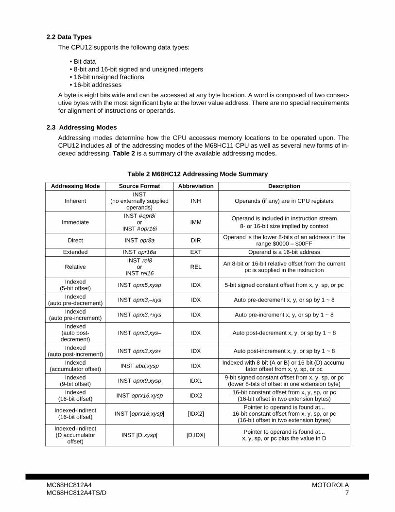
2.3 Addressing Modes
Addressing modes determine how the CPU accesses memory locations to be operated upon. TheCPU12 includes all of the addressing modes of the M68HC11 CPU as well as several new forms of in-dexed addressing. Table 2 is a summary of the available addressing modes.
Table 2 M68HC12 Addressing Mode Summary
Addressing Mode Source Format Abbreviation Description
InherentINST
(no externally supplied operands)
INH Operands (if any) are in CPU registers
ImmediateINST #opr8i
orINST #opr16i
IMMOperand is included in instruction stream
8- or 16-bit size implied by context
Direct INST opr8a DIR Operand is the lower 8-bits of an address in the range $0000 – $00FF
Extended INST opr16a EXT Operand is a 16-bit address
RelativeINST rel8
orINST rel16
REL An 8-bit or 16-bit relative offset from the current pc is supplied in the instruction
Indexed(5-bit offset) INST oprx5,xysp IDX 5-bit signed constant offset from x, y, sp, or pc
Indexed(auto pre-decrement) INST oprx3,–xys IDX Auto pre-decrement x, y, or sp by 1 ~ 8
Indexed(auto pre-increment) INST oprx3,+xys IDX Auto pre-increment x, y, or sp by 1 ~ 8
Indexed(auto post-decrement)
INST oprx3,xys– IDX Auto post-decrement x, y, or sp by 1 ~ 8
Indexed(auto post-increment) INST oprx3,xys+ IDX Auto post-increment x, y, or sp by 1 ~ 8
Indexed(accumulator offset) INST abd,xysp IDX Indexed with 8-bit (A or B) or 16-bit (D) accumu-
lator offset from x, y, sp, or pcIndexed
(9-bit offset) INST oprx9,xysp IDX1 9-bit signed constant offset from x, y, sp, or pc (lower 8-bits of offset in one extension byte)
Indexed(16-bit offset) INST oprx16,xysp IDX2 16-bit constant offset from x, y, sp, or pc
(16-bit offset in two extension bytes)
Indexed-Indirect(16-bit offset) INST [oprx16,xysp] [IDX2]
Pointer to operand is found at...16-bit constant offset from x, y, sp, or pc
(16-bit offset in two extension bytes)Indexed-Indirect(D accumulator
offset)INST [D,xysp] [D,IDX] Pointer to operand is found at...
x, y, sp, or pc plus the value in D
MC68HC812A4 MOTOROLAMC68HC812A4TS/D 7
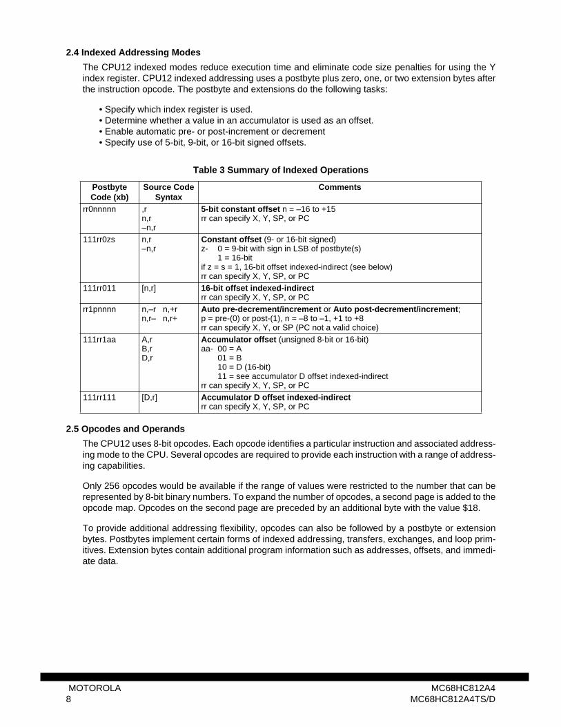
2.4 Indexed Addressing Modes
The CPU12 indexed modes reduce execution time and eliminate code size penalties for using the Yindex register. CPU12 indexed addressing uses a postbyte plus zero, one, or two extension bytes afterthe instruction opcode. The postbyte and extensions do the following tasks:
• Specify which index register is used.• Determine whether a value in an accumulator is used as an offset.• Enable automatic pre- or post-increment or decrement• Specify use of 5-bit, 9-bit, or 16-bit signed offsets.
2.5 Opcodes and Operands
The CPU12 uses 8-bit opcodes. Each opcode identifies a particular instruction and associated address-ing mode to the CPU. Several opcodes are required to provide each instruction with a range of address-ing capabilities.
Only 256 opcodes would be available if the range of values were restricted to the number that can berepresented by 8-bit binary numbers. To expand the number of opcodes, a second page is added to theopcode map. Opcodes on the second page are preceded by an additional byte with the value $18.
To provide additional addressing flexibility, opcodes can also be followed by a postbyte or extensionbytes. Postbytes implement certain forms of indexed addressing, transfers, exchanges, and loop prim-itives. Extension bytes contain additional program information such as addresses, offsets, and immedi-ate data.
Table 3 Summary of Indexed Operations
PostbyteCode (xb)
Source CodeSyntax
Comments
rr0nnnnn ,rn,r–n,r
5-bit constant offset n = –16 to +15rr can specify X, Y, SP, or PC
111rr0zs n,r–n,r
Constant offset (9- or 16-bit signed)z- 0 = 9-bit with sign in LSB of postbyte(s)
1 = 16-bitif z = s = 1, 16-bit offset indexed-indirect (see below)rr can specify X, Y, SP, or PC
111rr011 [n,r] 16-bit offset indexed-indirectrr can specify X, Y, SP, or PC
rr1pnnnn n,–r n,+rn,r– n,r+
Auto pre-decrement/increment or Auto post-decrement/increment ; p = pre-(0) or post-(1), n = –8 to –1, +1 to +8rr can specify X, Y, or SP (PC not a valid choice)
111rr1aa A,rB,rD,r
Accumulator offset (unsigned 8-bit or 16-bit)aa- 00 = A
01 = B10 = D (16-bit)11 = see accumulator D offset indexed-indirect
rr can specify X, Y, SP, or PC111rr111 [D,r] Accumulator D offset indexed-indirect
rr can specify X, Y, SP, or PC
MOTOROLA MC68HC812A48 MC68HC812A4TS/D

3 Pinout and Signal Descriptions
3.1 MC68HC812A4 Pin Assignments
The MC68HC812A4 is available in a 112-pin thin quad flat pack (TQFP). Most pins perform two or morefunctions, as described in the 3.2 Signal Descriptions . Figure 3 shows pin assignments.
Figure 3 Pin Assignments for MC68HC812A4
HC12 112TQFP
1 2 3 4 5 6 7 8 9 10 11 12 13 14 15 16 17 18 19 20 21 22 23 24 25 26 27 28
VS
SX
VD
DX
KW
J0/P
J0K
WJ1
/PJ1
KW
J2/P
J2K
WJ3
/PJ3
KW
J4/P
J4K
WJ5
/PJ5
KW
J6/P
J6K
WJ7
/PJ7
AD
DR
16/P
G0
AD
DR
17/P
G1
AD
DR
18/P
G2
VD
DV
SS
AD
DR
19/P
G3
AD
DR
20/P
G4
AD
DR
21/P
G5
BK
GD
/ TAG
HI
DAT
A0/
KW
D0/
PD
0D
ATA
1/K
WD
1/P
D1
DAT
A2/
KW
D2/
PD
2D
ATA
3/K
WD
3/P
D3
DAT
A4/
KW
D4/
PD
4D
ATA
5/K
WD
5/P
D5
DAT
A6/
KW
D6/
PD
6D
ATA
7/K
WD
7/P
D7
DAT
A8/
PC
0
MC68HC812A4112TQFP
29303132333435363738394041424344454647484950515253545556
DATA9/PC1DATA10/PC2DATA11/PC3DATA12/PC4DATA13/PC5DATA14/PC6DATA15/PC7XIRQ/PE0IRQ/VPP/PE1R/W/PE2LSTRB/TAGLO/PE3RESETVSSX
VDDX
VDDPLL
XFCVSSPLL
EXTALXTALECLK/PE4MODA/IPIPE0/PE5MODB/IPIPE1/PE6ARST/PE7ADDR0/PB0ADDR1/PB1ADDR2/PB2ADDR3/PB3ADDR4/PB4
PH
7/K
WH
7P
H6/
KW
H6
PH
5/K
WH
5P
H4/
KW
H4
VS
SX
VD
DX
PH
3/K
WH
3P
H2/
KW
H2
PH
1/K
WH
1P
H0/
KW
H0
PF
6/CS
P1
PF
5/CS
P0
PF
4/CS
DP
F3/C
S3
PF
2/CS
2P
F1/C
S1
PF
0/CS
0PA
7/A
DD
R15
PA6/
AD
DR
14PA
5/A
DD
R13
PA4/
AD
DR
12PA
3/A
DD
R11
PA2/
AD
DR
10PA
1/A
DD
R9
PA0/
AD
DR
8P
B7/
AD
DR
7P
B6/
AD
DR
6P
B5/
AD
DR
5
84 83 82 81 80 79 78 77 76 75 74 73 72 71 70 69 68 67 66 65 64 63 62 61 60 59 58 57
PT7/IOC7/PAIPT6/IOC6PT5/IOC5PT4/IOC4PT3/IOC3PT2/IOC2PT1/IOC1PT0/IOC0
PS7/SSPS6/SCK
PS5/SDO/MOSIPS4/SDI/MISO
PS3/TxD1PS2/RxD1PS1/TxD0PS0/RxD0
VSSA
VDDA
PAD7/AN7/VSTBY
PAD6/AN6PAD5/AN5PAD4/AN4PAD3/AN3PAD2/AN2PAD1/AN1PAD0/AN0
VRL
VRH
112111110109108107106105104103102101100999897969594939291908988878685
MC68HC812A4 MOTOROLAMC68HC812A4TS/D 9

3.2 Signal Descriptions
MC68HC812A4 pins and signals are described in Table 4 . Individual ports are cross referenced inTable 5 .
Table 4 MC68HC812A4 Signal Descriptions
Mnemonic Port DescriptionVDD, VSS
— VDD is the power supply, and VSS is ground. The MCU operates from a sin-gle power supply. Use customary bypass techniques as very fast signal tran-sitions occur on the MCU pins.
VRH, VRL — Provide the reference voltage for the analog-to-digital converter.
AVDD, AVSS — Provides the operating voltage and ground for the analog-to-digital convert-er. This allows the supply voltage to the ATD to be bypassed independently.
VDDPLL,VSSPLL
— Power and ground for PLL clock control; allows independent supply voltage to the PLL.
VSTBY Port AD VSTBY is used to imput RAM standby power.
XTAL,EXTAL
— Crystal driver and external clock input pins provide the interface for either a crystal or a CMOS compatible clock to control the internal clock generator circuitry. Out of reset the frequency applied to EXTAL is two times higher than the desired E-clock rate. On reset all the device clocks are derived from the EXTAL input frequency. XTAL is the crystal output.
XIRQ PE0 Provides a means of requesting a non-maskable interrupt request after reset initialization.
IRQ PE1 Maskable interrupt request input provides a means of applying asynchro-nous interrupt requests to the MCU. Either falling edge-sensitive triggering or level-sensitive triggering is program selectable (INTCR register).
R/W PE2 Indicates direction of data on expansion bus. Shares function with general-purpose I/O. Read/write in expanded modes.
LSTRB PE3 Low byte strobe (0 = low byte valid), in all modes this pin can be used asI/O. The low strobe function is the exclusive-NOR of A0 and the internal SZ8 signal. (The SZ8 internal signal indicates the size 16/8 access.)
ECLK PE4 E-clock is the output connection for the external bus clock. ECLK is used as a timing reference. The unstretched ECLK frequency is normally equal to 1/2 the crystal frequency. Can be general-purpose I/O.
BKGD — State of mode select pins during reset determine the initial operating mode of the MCU. After reset, MODA and MODB can be configured as instruction queue tracking signals IPIPE0 and IPIPE1 or as general-purpose I/O pins.
MODA PE5MODB PE6IPIPE0 PE5 Instruction queue tracking signals can be used by a development system to
reconstruct the instruction queue and track instruction execution.IPIPE1 PE6ARST PE7 Alternate reset input or general-purpose I/O. It can be used as a separate
controlled active-high reset input.XFC — Loop filter pin for controlled damping of the PLL VCO loop.
RESET — An active low bidirectional control signal, RESET acts as an input to initialize the MCU to a known start-up state, and an output when COP or clock mon-itor causes a reset.
ADDR[15:8] Port A External bus pins share function with general-purpose I/O ports A, B, C, and D. In single-chip operating modes, the pins can be used for I/O; in expanded modes, the pins are used for the external buses. In narrow data bus mode, port D is available as standard I/O or key wakeup inputs.
ADDR[7:0] Port BDATA[15:8] Port CDATA[7:0] Port D
ADDR[21:16] Port G Memory expansion and general-purpose I/O.CS[3:0]
CSDCSP[1:0]
Port F Chip selects and general-purpose I/O.
MOTOROLA MC68HC812A410 MC68HC812A4TS/D

BKGD — Single-wire background interface pin is dedicated to the background debug function. During reset, this pin determines special or normal operating mode.
KWD[7:0] Port D Key wakeup and general-purpose I/O; can cause an interrupt when an input transitions from high to low.KWH[7:0] Port H
KWJ[7:0] Port J Key wakeup and general-purpose I/O; can cause an interrupt when an input transitions from high to low or from low to high.
RxD0 PS0 Serial communications interface receive pin for SCI0.TxD0 PS1 Serial communications interface transmit pin for SCI0.RxD1 PS2 Serial communications interface receive pin for SCI1.TxD1 PS3 Serial communications interface transmit pin for SCI1.
SDI/MISO PS4 Master in/slave out pin for serial peripheral interface.SDO/MOSI PS5 Master out/slave in pin for serial peripheral interface.
SCK PS6 Serial clock for SPI system.SS PS7 Slave select output for SPI master mode, input for slave mode.
IOC[7:0] Port T Input capture or output compare channels and pulse accumulator input.
Table 5 Port Descriptions
PortName Direction FunctionPort A In/Out General-purpose I/O in single-chip modes. External address bus ADDR[15:8]
in expanded modes.Port B In/Out General-purpose I/O in single-chip modes. External address bus ADDR[7:0] in
expanded modes.Port C In/Out General-purpose I/O in single-chip modes. External data bus DATA[15:8] in ex-
panded wide modes; external data bus DATA[15:8]/DATA[7:0] in expanded narrow modes.
Port D In/Out General-purpose I/O in single-chip modes and expanded narrow modes. Exter-nal data bus DATA[7:0] in expanded wide mode. As key wakeup can cause an interrupt when an input transitions from high to low.
Port E PE[1:0] InPE[7:2] In/Out
Mode selection, bus control signals and interrupt service request signals; or general-purpose I/O.
Port F In/Out Chip select and general-purpose I/O.Port G In/Out Memory expansion and general-purpose I/O.Port H In/Out Key wakeup and general-purpose I/O, can cause an interrupt when an input
transitions from high to low.Port J In/Out Key wakeup and general-purpose I/O, can cause an interrupt when an input
transitions from high to low or from low to high.Port S In/Out Serial communications interface and serial peripheral interface subsystems
and general-purpose I/O.Port T In/Out Timer system and general-purpose I/O.
Port AD In Analog-to-digital converter and general-purpose input.
Table 4 MC68HC812A4 Signal Descriptions (Continued)
Mnemonic Port Description
MC68HC812A4 MOTOROLAMC68HC812A4TS/D 11
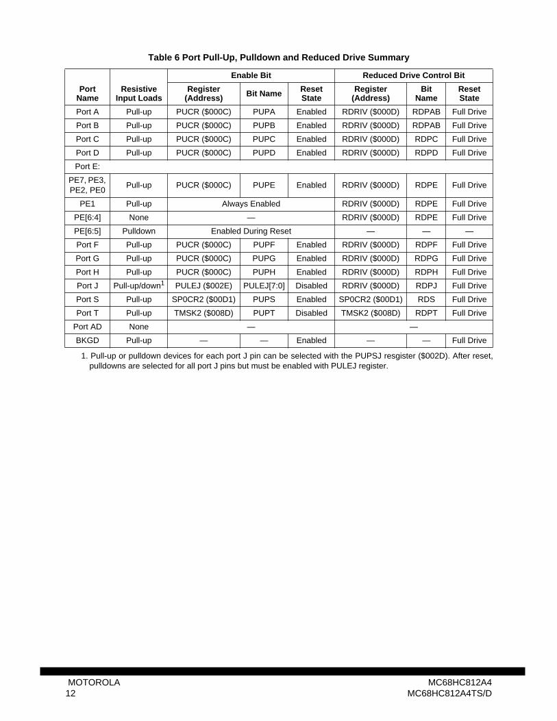
1. Pull-up or pulldown devices for each port J pin can be selected with the PUPSJ resgister ($002D). After reset,pulldowns are selected for all port J pins but must be enabled with PULEJ register.
Table 6 Port Pull-Up, Pulldown and Reduced Drive Summary
Enable Bit Reduced Drive Control Bit
PortName
ResistiveInput Loads
Register(Address) Bit Name Reset
StateRegister
(Address)Bit
NameReset State
Port A Pull-up PUCR ($000C) PUPA Enabled RDRIV ($000D) RDPAB Full Drive
Port B Pull-up PUCR ($000C) PUPB Enabled RDRIV ($000D) RDPAB Full Drive
Port C Pull-up PUCR ($000C) PUPC Enabled RDRIV ($000D) RDPC Full Drive
Port D Pull-up PUCR ($000C) PUPD Enabled RDRIV ($000D) RDPD Full Drive
Port E:
PE7, PE3, PE2, PE0
Pull-up PUCR ($000C) PUPE Enabled RDRIV ($000D) RDPE Full Drive
PE1 Pull-up Always Enabled RDRIV ($000D) RDPE Full Drive
PE[6:4] None — RDRIV ($000D) RDPE Full Drive
PE[6:5] Pulldown Enabled During Reset — — —
Port F Pull-up PUCR ($000C) PUPF Enabled RDRIV ($000D) RDPF Full Drive
Port G Pull-up PUCR ($000C) PUPG Enabled RDRIV ($000D) RDPG Full Drive
Port H Pull-up PUCR ($000C) PUPH Enabled RDRIV ($000D) RDPH Full Drive
Port J Pull-up/down1 PULEJ ($002E) PULEJ[7:0] Disabled RDRIV ($000D) RDPJ Full Drive
Port S Pull-up SP0CR2 ($00D1) PUPS Enabled SP0CR2 ($00D1) RDS Full Drive
Port T Pull-up TMSK2 ($008D) PUPT Disabled TMSK2 ($008D) RDPT Full Drive
Port AD None — —
BKGD Pull-up — — Enabled — — Full Drive
MOTOROLA MC68HC812A412 MC68HC812A4TS/D

4 Register BlockThe register block can be mapped to any 2-Kbyte boundary within the standard 64-Kbyte address spaceby manipulating bits REG[15:11] in the INITRG register. INITRG establishes the upper five bits of theregister block’s 16-bit address. The register block occupies the first 512 bytes of the 2-Kbyte block. De-fault addressing (after reset) is indicated in the table below. For additional information refer to 6 Oper-ating Modes and Resource Mapping .
Table 7 MC68HC812A4 Register Map (Sheet 1 of 4)
Address Bit 7 6 5 4 3 2 1 Bit 0 Name$0000 PA7 PA6 PA5 PA4 PA3 PA2 PA1 PA0 PORTA1
$0001 PB7 PB6 PB5 PB4 PB3 PB2 PB1 PB0 PORTB1
$0002 Bit 7 6 5 4 3 2 1 Bit 0 DDRA1
$0003 Bit 7 6 5 4 3 2 1 Bit 0 DDRB1
$0004 PC7 PC6 PC5 PC4 PC3 PC2 PC1 PC0 PORTC1
$0005 PD7 PD6 PD5 PD4 PD3 PD2 PD1 PD0 PORTD2
$0006 Bit 7 6 5 4 3 2 1 Bit 0 DDRC1
$0007 Bit 7 6 5 4 3 2 1 Bit 0 DDRD2
$0008 PE7 PE6 PE5 PE4 PE3 PE2 PE1 PE0 PORTE3
$0009 Bit 7 Bit 6 Bit 5 Bit 4 Bit 3 Bit 2 0 0 DDRE3
$000A ARSIE PLLTE PIPOE NECLK LSTRE RDWE 0 0 PEAR4
$000B SMODN MODB MODA ESTR IVIS 0 EMD EME MODE4
$000C PUPH PUPG PUPF PUPE PUPD PUPC PUPB PUPA PUCR4
$000D RDPJ RDPH RDPG RDPF RDPE RDPD RDPC RDPAB RDRIV4
$000E 0 0 0 0 0 0 0 0 Reserved4
$000F 0 0 0 0 0 0 0 0 Reserved4
$0010 RAM15 RAM14 RAM13 RAM12 RAM11 0 0 0 INITRM$0011 REG15 REG14 REG13 REG12 REG11 0 0 0 INITRG$0012 EE15 EE14 EE13 EE12 0 0 0 EEON INITEE$0013 EWDIR NDRC 0 0 0 0 0 0 MISC$0014 RTIE RSWAI RSBCK 0 RTBYP RTR2 RTR1 RTR0 RTICTL$0015 RTIF 0 0 0 0 0 0 0 RTIFLG$0016 CME FCME FCM FCOP DISR CR2 CR1 CR0 COPCTL$0017 Bit 7 6 5 4 3 2 1 Bit 0 COPRST$0018 ITE6 ITE8 ITEA ITEC ITEE ITF0 ITF2 ITF4 ITST0$0019 ITD6 ITD8 ITDA ITDC ITDE ITE0 ITE2 ITE4 ITST1$001A ITC6 ITC8 ITCA ITCC ITCE ITD0 ITD2 ITD4 ITST2$001B 0 0 0 0 0 ITC0 ITC2 ITC4 ITST3$001C 0 0 0 0 0 0 0 0 Reserved$001D 0 0 0 0 0 0 0 0 Reserved$001E IRQE IRQEN DLY 0 0 0 0 0 INTCR$001F 1 1 PSEL5 PSEL4 PSEL3 PSEL2 PSEL1 0 HPRIO$0020 Bit 7 6 5 4 3 2 1 Bit 0 KWIED5
$0021 Bit 7 6 5 4 3 2 1 Bit 0 KWIFD5
$0022 0 0 0 0 0 0 0 0 Reserved$0023 0 0 0 0 0 0 0 0 Reserved$0024 PH7 PH6 PH5 PH4 PH3 PH2 PH1 PH0 PORTH$0025 Bit 7 6 5 4 3 2 1 Bit 0 DDRH$0026 Bit 7 6 5 4 3 2 1 Bit 0 KWIEH$0027 Bit 7 6 5 4 3 2 1 Bit 0 KWIFH$0028 PJ7 PJ6 PJ5 PJ4 PJ3 PJ2 PJ1 PJ0 PORTJ
MC68HC812A4 MOTOROLAMC68HC812A4TS/D 13

$0029 Bit 7 6 5 4 3 2 1 Bit 0 DDRJ$002A Bit 7 6 5 4 3 2 1 Bit 0 KWIEJ$002B Bit 7 6 5 4 3 2 1 Bit 0 KWIFJ$002C Bit 7 6 5 4 3 2 1 Bit 0 KPOLJ$002D Bit 7 6 5 4 3 2 1 Bit 0 PUPSJ$002E Bit 7 6 5 4 3 2 1 Bit 0 PULEJ$002F 0 0 0 0 0 0 0 0 Reserved$0030 0 PF6 PF5 PF4 PF3 PF2 PF1 PF0 PORTF$0031 0 0 PG5 PG4 PG3 PG2 PG1 PG0 PORTG$0032 0 Bit 6 5 4 3 2 1 Bit 0 DDRF$0033 0 0 Bit 5 4 3 2 1 Bit 0 DDRG$0034 PDA19 PDA18 PDA17 PDA16 PDA15 PDA14 PDA13 PDA12 DPAGE$0035 PPA21 PPA20 PPA19 PPA18 PPA17 PPA16 PPA15 PPA14 PPAGE$0036 PEA17 PEA16 PEA15 PEA14 PEA13 PEA12 PEA11 PEA10 EPAGE$0037 DWEN PWEN EWEN 0 0 0 0 0 WINDEF$0038 0 0 A21E A20E A19E A18E A17E A16E MXAR$0039 0 0 0 0 0 0 0 0 Reserved$003A 0 0 0 0 0 0 0 0 Reserved$003B 0 0 0 0 0 0 0 0 Reserved$003C 0 CSP1E CSP0E CSDE CS3E CS2E CS1E CS0E CSCTL0$003D 0 CSP1FL CSPA21 CSDHF CS3EP 0 0 0 CSCTL1$003E 0 0 SRP1A SRP1B SRP0A SRP0B STRDA STRDB CSSTR0$003F STR3A STR3B STR2A STR2B STR1A STR1B STR0A STR0B CSSTR1$0040 0 0 0 0 LDV11 LDV10 LDV9 LDV8 LDV$0041 LDV7 LDV6 LDV5 LDV4 LDV3 LDV2 LDV1 LDV0 LDV$0042 0 0 0 0 RDV11 RDV10 RDV9 RDV8 RDV$0043 RDV7 RDV6 RDV5 RDV4 RDV3 RDV2 RDV1 RDV0 RDV$0044 0 0 0 0 0 0 0 0 Reserved$0045 0 0 0 0 0 0 0 0 Reserved$0046 0 0 0 0 0 0 0 0 Reserved$0047 LCK PLLON PLLS BCSC BCSB BCSA MCSB MCSA CLKCTL
$0048–$005F 0 0 0 0 0 0 0 0 Reserved
$0060 0 0 0 0 0 0 0 0 ATDCTL0$0061 0 0 0 0 0 0 0 0 ATDCTL1$0062 ADPU AFFC AWAI 0 0 0 ASCIE ASCIF ATDCTL2$0063 0 0 0 0 0 0 FRZ1 FRZ0 ATDCTL3$0064 0 SMP1 SMP0 PRS4 PRS3 PRS2 PRS1 PRS0 ATDCTL4$0065 0 S8CM SCAN MULT CD CC CB CA ATDCTL5$0066 SCF 0 0 0 0 CC2 CC1 CC0 ATDSTAT$0067 CCF7 CCF6 CCF5 CCF4 CCF3 CCF2 CCF1 CCF0 ATDSTAT$0068 SAR9 SAR8 SAR7 SAR6 SAR5 SAR4 SAR3 SAR2 ATDTEST$0069 SAR1 SAR0 RST TSTOUT TST3 TST2 TST1 TST0 ATDTEST
$006A–$006E 0 0 0 0 0 0 0 0 Reserved
$006F PAD7 PAD6 PAD5 PAD4 PAD3 PAD2 PAD1 PAD0 PORTAD$0070 Bit 7 6 5 4 3 2 1 Bit 0 ADR0H$0071 0 0 0 0 0 0 0 0 Reserved$0072 Bit 7 6 5 4 3 2 1 Bit 0 ADR1H
Table 7 MC68HC812A4 Register Map (Sheet 2 of 4)
Address Bit 7 6 5 4 3 2 1 Bit 0 Name
MOTOROLA MC68HC812A414 MC68HC812A4TS/D
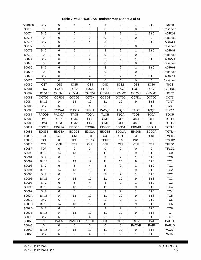
$0073 0 0 0 0 0 0 0 0 Reserved$0074 Bit 7 6 5 4 3 2 1 Bit 0 ADR2H$0075 0 0 0 0 0 0 0 0 Reserved$0076 Bit 7 6 5 4 3 2 1 Bit 0 ADR3H$0077 0 0 0 0 0 0 0 0 Reserved$0078 Bit 7 6 5 4 3 2 1 Bit 0 ADR4H$0079 0 0 0 0 0 0 0 0 Reserved$007A Bit 7 6 5 4 3 2 1 Bit 0 ADR5H$007B 0 0 0 0 0 0 0 0 Reserved$007C Bit 7 6 5 4 3 2 1 Bit 0 ADR6H$007D 0 0 0 0 0 0 0 0 Reserved$007E Bit 7 6 5 4 3 2 1 Bit 0 ADR7H$007F 0 0 0 0 0 0 0 0 Reserved$0080 IOS7 IOS6 IOS5 IOS4 IOS3 IOS2 IOS1 IOS0 TIOS$0081 FOC7 FOC6 FOC5 FOC4 FOC3 FOC2 FOC1 FOC0 CFORC$0082 OC7M7 OC7M6 OC7M5 OC7M4 OC7M3 OC7M2 OC7M1 OC7M0 OC7M$0083 OC7D7 OC7D6 OC7D5 OC7D4 OC7D3 OC7D2 OC7D1 OC7D0 OC7D$0084 Bit 15 14 13 12 11 10 9 Bit 8 TCNT$0085 Bit 7 6 5 4 3 2 1 Bit 0 TCNT$0086 TEN TSWAI TSBCK TFFCA PAOQE T7QE T1QE T0QE TSCR$0087 PAOQB PAOQA T7QB T7QA T1QB T1QA T0QB T0QA TQCR$0088 OM7 OL7 OM6 OL6 OM5 OL5 OM4 OL4 TCTL1$0089 OM3 OL3 OM2 OL2 OM1 OL1 OM0 OL0 TCTL2$008A EDG7B EDG7A EDG6B EDG6A EDG5B EDG5A EDG4B EDG4A TCTL3$008B EDG3B EDG3A EDG2B EDG2A EDG1B EDG1A EDG0B EDG0A TCTL4$008C C7I C6I C5I C4I C3I C2I C1I C0I TMSK1$008D TOI 0 TPU TDRB TCRE PR2 PR1 PR0 TMSK2$008E C7F C6F C5F C4F C3F C2F C1F C0F TFLG1$008F TOF 0 0 0 0 0 0 0 TFLG2$0090 Bit 15 14 13 12 11 10 9 Bit 8 TC0$0091 Bit 7 6 5 4 3 2 1 Bit 0 TC0$0092 Bit 15 14 13 12 11 10 9 Bit 8 TC1$0093 Bit 7 6 5 4 3 2 1 Bit 0 TC1$0094 Bit 15 14 13 12 11 10 9 Bit 8 TC2$0095 Bit 7 6 5 4 3 2 1 Bit 0 TC2$0096 Bit 15 14 13 12 11 10 9 Bit 8 TC3$0097 Bit 7 6 5 4 3 2 1 Bit 0 TC3$0098 Bit 15 14 13 12 11 10 9 Bit 8 TC4$0099 Bit 7 6 5 4 3 2 1 Bit 0 TC4$009A Bit 15 14 13 12 11 10 9 Bit 8 TC5$009B Bit 7 6 5 4 3 2 1 Bit 0 TC5$009C Bit 15 14 13 12 11 10 9 Bit 8 TC6$009D Bit 7 6 5 4 3 2 1 Bit 0 TC6$009E Bit 15 14 13 12 11 10 9 Bit 8 TC7$009F Bit 7 6 5 4 3 2 1 Bit 0 TC7$00A0 0 PAEN PAMOD PEDGE CLK1 CLK0 PAOVI PAI PACTL$00A1 0 0 0 0 0 0 PAOVF PAIF PAFLG$00A2 Bit 15 14 13 12 11 10 9 Bit 8 PACNT$00A3 Bit 7 6 5 4 3 2 1 Bit 0 PACNT
Table 7 MC68HC812A4 Register Map (Sheet 3 of 4)
Address Bit 7 6 5 4 3 2 1 Bit 0 Name
MC68HC812A4 MOTOROLAMC68HC812A4TS/D 15

1. Port A, port B, port C and data direction registers DDRA, DDRB, and DDRC are not in map inexpanded and peripheral modes.
2. Port D and DDRD not in map in wide expanded modes and peripheral mode; also not in mapin narrow special expanded mode with EMD set.
3. Port E and DDRE not in map in peripheral mode; also not in map in expanded modes withEME set.
4. Registers also not in map in peripheral mode.5. Key wake-up associated with port D not in map in wide expanded modes; also not in map in
narrow special expanded mode with EMD set.
$00A4–$00AC 0 0 0 0 0 0 0 0 Reserved
$00AD 0 0 0 0 0 0 TCBYP PCBYP TIMTST$00AE PT7 PT6 PT5 PT4 PT3 PT2 PT1 PT0 PORTT$00AF Bit 7 6 5 4 3 2 1 Bit 0 DDRT$00B0–$00BF 0 0 0 0 0 0 0 0 Reserved
$00C0 BTST BSPL BRLD SBR12 SBR11 SBR10 SBR9 SBR8 SC0BDH$00C1 SBR7 SBR6 SBR5 SBR4 SBR3 SBR2 SBR1 SBR0 SC0BDL$00C2 LOOPS WOMS RSRC M WAKE ILT PE PT SC0CR1$00C3 TIE TCIE RIE ILIE TE RE RWU SBK SC0CR2$00C4 TDRE TC RDRF IDLE OR NF FE PF SC0SR1$00C5 0 0 0 0 0 0 0 RAF SC0SR2$00C6 R8 T8 0 0 0 0 0 0 SC0DRH$00C7 R7T7 R6T6 R5T5 R4T4 R3T3 R2T2 R1T1 R0T0 SC0DRL$00C8 BTST BSPL BRLD SBR12 SBR11 SBR10 SBR9 SBR8 SC1BDH$00C9 SBR7 SBR6 SBR5 SBR4 SBR3 SBR2 SBR1 SBR0 SC1BDL$00CA LOOPS WOMS RSRC M WAKE ILT PE PT SC1CR1$00CB TIE TCIE RIE ILIE TE RE RWU SBK SC1CR2$00CC TDRE TC RDRF IDLE OR NF FE PF SC1SR1$00CD 0 0 0 0 0 0 0 RAF SC1SR2$00CE R8 T8 0 0 0 0 0 0 SC1DRH$00CF R7T7 R6T6 R5T5 R4T4 R3T3 R2T2 R1T1 R0T0 SC1DRL$00D0 SPIE SPE SWOM MSTR CPOL CPHA SSOE LSBF SP0CR1$00D1 SPFQE SPFQB SPFQA 0 PUPS RDS 0 SPC0 SP0CR2$00D2 0 0 0 0 0 SPR2 SPR1 SPR0 SP0BR$00D3 SPIF WCOL 0 MODF 0 0 0 0 SP0SR$00D4 0 0 0 0 0 0 0 0 Reserved$00D5 Bit 7 6 5 4 3 2 1 Bit 0 SP0DR$00D6 PS7 PS6 PS5 PS4 PS3 PS2 PS1 PS0 PORTS$00D7 Bit 7 6 5 4 3 2 1 Bit 0 DDRS
$00D8–$00DF 0 0 0 0 0 0 0 0 Reserved
$00E0– $00EF 0 0 0 0 0 0 0 0 Reserved
$00F0 1 1 1 1 1 1 PROTLCK EERC EEMCR$00F1 1 BPROT6 BPROT5 BPROT4 BPROT3 BPROT2 BPROT1 BPROT0 EEPROT$00F2 EEODD EEVEN MARG EECPD EECPRD 0 EECPM 0 EETST$00F3 BULKP 0 0 BYTE ROW ERASE EELAT EEPGM EEPROG
$00F4– $01FF 0 0 0 0 0 0 0 0 Reserved
Table 7 MC68HC812A4 Register Map (Sheet 4 of 4)
Address Bit 7 6 5 4 3 2 1 Bit 0 Name
MOTOROLA MC68HC812A416 MC68HC812A4TS/D

5 Bus Control and Input/OutputInternally the MC68HC812A4 has full 16-bit data paths, but depending upon the operating mode andcontrol registers, the external bus may be 8 or 16 bits. There are cases where 8-bit and 16-bit accessescan appear on adjacent cycles using the LSTRB signal to indicate 8- or 16-bit data.
5.1 Detecting Access Type from External Signals
The external signals LSTRB, R/W, and A0 can be used to determine the type of bus access that is tak-ing place. Accesses to the internal RAM module are the only type of access that produce LSTRB = A0= 1, because the internal RAM is specifically designed to allow misaligned 16-bit accesses in a singlecycle. In these cases the data for the address that was accessed is on the low half of the data bus andthe data for address + 1 is on the high half of the data bus.
5.2 Registers
Not all registers are visible in the MC68HC812A4 memory map under certain conditions. In special pe-ripheral mode the first 16 registers associated with bus expansion are removed from the memory map.
In expanded modes, some or all of port A, port B, port C, port D, and port E are used for expansionbuses and control signals. In order to allow emulation of the single-chip functions of these ports, someof these registers must be rebuilt in an external port replacement unit. In any expanded mode, port A,port B, and port C are used for address and data lines so registers for these ports, as well as the datadirection registers for these ports, are removed from the on-chip memory map and become external ac-cesses.
Port D and its associated data direction register may be removed from the on-chip map when port D isneeded for 16-bit data transfers. If the MCU is in an expanded wide mode, port C and port D are usedfor 16-bit data and the associated port and data direction registers become external accesses. Whenthe MCU is in expanded narrow mode, the external data bus is normally 8-bits. To allow full-speed op-eration while allowing visibility of internal 16-bit accesses, a 16-bit-wide data path is required. The em-ulate port D (EMD) control bit in the MODE register may be set to allow such 16-bit transfers. In thiscase of narrow special expanded mode and the EMD bit set, port D and data direction D registers areremoved form the on-chip memory map and become external accesses so port D may be rebuilt exter-nally.
In any expanded mode, port E pins may be needed for bus control (e.g., ECLK, R/W). To regain thesingle-chip functions of port E, the emulate port E (EME) control bit in the MODE register may be set.In this special case of expanded mode and EME set, PORTE and DDRE registers are removed fromthe on-chip memory map and become external accesses so port E may be rebuilt externally.
Table 8 Access Type vs. Bus Control Pins
LSTRB A0 R/W Type of Access1 0 1 8-bit read of an even address0 1 1 8-bit read of an odd address1 0 0 8-bit write of an even address0 1 0 8-bit write of an odd address0 0 1 16-bit read of an even address1 1 1 16-bit read of an odd address
(low/high data swapped)0 0 0 16-bit write to an even address1 1 0 16-bit write to an even address
(low/high data swapped)
MC68HC812A4 MOTOROLAMC68HC812A4TS/D 17

Bits PA[7:0] are associated with addresses ADDR[15:8] respectively. When this port is not used for ex-ternal addresses such as in single-chip mode, these pins can be used as general-purpose I/O. DDRAdetermines the primary direction of each pin. This register is not in the on-chip map in expanded andperipheral modes. Read and write anytime.
This register determines the primary direction for each port A pin when functioning as a general-purposeI/O port. DDRA is not in the on-chip map in expanded and peripheral modes. Read and write anytime.
0 = Associated pin is a high-impedance input1 = Associated pin is an output
Bits PB[7:0] are associated with addresses ADDR[7:0] respectively. When this port is not used for ex-ternal addresses such as in single-chip mode, these pins can be used as general-purpose I/O. DDRBdetermines the primary direction of each pin. This register is not in the on-chip map in expanded andperipheral modes. Read and write anytime.
This register determines the primary direction for each port B pin when functioning as a general-purposeI/O port. DDRB is not in the on-chip map in expanded and peripheral modes. Read and write anytime.
0 = Associated pin is a high-impedance input1 = Associated pin is an output
PORTA — Port A Register $0000
Bit 7 6 5 4 3 2 1 Bit 0Single Chip PA7 PA6 PA5 PA4 PA3 PA2 PA1 PA0
RESET: 0 0 0 0 0 0 0 0Expanded& Periph:
ADDR15 ADDR14 ADDR13 ADDR12 ADDR11 ADDR10 ADDR9 ADDR8
DDRA — Port A Data Direction Register $0002
Bit 7 6 5 4 3 2 1 Bit 0Bit 7 6 5 4 3 2 1 Bit 0
RESET: 0 0 0 0 0 0 0 0
PORTB — Port B Register $0001
Bit 7 6 5 4 3 2 1 Bit 0Single Chip PB7 PB6 PB5 PB4 PB3 PB2 PB1 PB0
RESET: 0 0 0 0 0 0 0 0Expanded& Periph:
ADDR7 ADDR6 ADDR5 ADDR4 ADDR3 ADDR2 ADDR1 ADDR0
DDRB — Port B Data Direction Register $0003
Bit 7 6 5 4 3 2 1 Bit 0Bit 7 6 5 4 3 2 1 Bit 0
RESET: 0 0 0 0 0 0 0 0
MOTOROLA MC68HC812A418 MC68HC812A4TS/D

Bits PC[7:0] are associated with DATA[15:8] respectively. When this port is not used for external datasuch as in single-chip mode, these pins can be used as general-purpose I/O. DDRC determines theprimary direction for each pin. In narrow expanded modes, DATA[15:8] and DATA[7:0] are multiplexedinto the MCU through port C pins on successive cycles. This register is not in the on-chip map in ex-panded and peripheral modes.
Read and write anytime (provided this register is in the map).
When the MCU is operating in special expanded narrow mode and port C and port D are being usedfor internal visibility, internal accesses produce full 16-bit information with DATA[15:8] on port C andDATA[7:0] on port D. This allows the MCU to operate at full speed while making 16-bit access informa-tion available to external development equipment in a single cycle. In this narrow mode, normal 16-bitaccesses to external memory get split into two successive 8-bit accesses on port C alone.
This register determines the primary direction for each port C pin when functioning as a general-pur-pose I/O port. DDRC is not in the on-chip map in expanded and peripheral modes. Read and write any-time.
0 = Associated pin is a high-impedance input1 = Associated pin is an output
Bits PD[7:0] are associated with DATA[7:0] respectively. When this port is not used for external data,such as in single-chip mode, these pins can be used as general-purpose I/O or key wakeup signals.DDRD determines the primary direction of each port D pin.
In special expanded narrow mode the external data bus is normally limited to eight bits on port C butthe emulate port D (EMD) control bit in the MODE register can be set to allow port C and port D to beused together to provide single-cycle visibility of internal 16-bit accesses for debugging purposes. If themode is special narrow expanded and EMD is set, port D is configured for DATA[7:0] of visible internalaccesses and normal 16-bit external accesses are split into two adjacent 8-bit accesses through portC. This allows connection of a single 8-bit external program memory.
PORTC — Port C Register $0004
Bit 7 6 5 4 3 2 1 Bit 0Single Chip PC7 PC6 PC5 PC4 PC3 PC2 PC1 PC0
RESET: 0 0 0 0 0 0 0 0Exp Wide &
PeriphDATA15 DATA14 DATA13 DATA12 DATA11 DATA10 DATA9 DATA8
Expanded Narrow
DATA15/7 DATA14/6 DATA13/5 DATA12/4 DATA11/3 DATA10/2 DATA9/1 DATA8/0
DDRC — Port C Data Direction Register $0006
Bit 7 6 5 4 3 2 1 Bit 0Bit 7 6 5 4 3 2 1 Bit 0
RESET: 0 0 0 0 0 0 0 0
PORTD — Port D Register $0005
Sgl Chip & Bit 7 6 5 4 3 2 1 Bit 0 Exp Narrow PD7 PD6 PD5 PD4 PD3 PD2 PD1 PD0
RESET: 0 0 0 0 0 0 0 0Exp Wide &
Periph DATA7 DATA6 DATA5 DATA4 DATA3 DATA2 DATA1 DATA0
Alt. Pin Function KWD7 KWD6 KWD5 KWD4 KWD3 KWD2 KWD1 KWD0
MC68HC812A4 MOTOROLAMC68HC812A4TS/D 19

This register is not in the on-chip map in wide expanded and peripheral modes. Also, in special narrowexpanded mode, the function of this port is determined by the EMD control bit. If EMD is set, this registeris not in the on-chip map and port D is used for DATA[7:0] of visible internal accesses. If EMD is clear,this port serves as general-purpose I/O or key wakeup signals. Read and write anytime.
When port D is operating as a general-purpose I/O port, this register determines the primary directionfor each port D pin.
0 = Associated pin is a high-impedance input1 = Associated pin is an output
This register is not in the map in wide expanded and peripheral modes. Also, in special narrow expand-ed mode, the function of this port is determined by the EMD control bit. If EMD is set, this register is notin the on-chip map and port D is used for DATA[7:0] of visible internal accesses. If EMD is clear, thisport serves as general-purpose I/O or key wakeup signals.
Read and write anytime.
This register is associated with external bus control signals and interrupt inputs including auxiliary reset(ARST), mode select (MODB/IPIPE1, MODA/IPIPE0), E clock, size (LSTRB), read/write (R/W), IRQ,and XIRQ. When the associated pin is not used for one of these specific functions, the pin can be usedas general-purpose I/O. The port E assignment register (PEAR) selects the function of each pin. DDREdetermines the primary direction of each port E pin when configured to be general-purpose I/O.
Some of these pins have software selectable pull-ups (LSTRB, R/W, and XIRQ). A single control bit en-ables the pull-ups for all these pins which are configured as inputs. IRQ always has a pull-up.
PE7 can be selected as a high-true auxiliary reset input.
This register is not in the map in peripheral mode or expanded modes when the EME bit is set.
Read and write anytime.
DDRD — Port D Data Direction Register $0007
Bit 7 6 5 4 3 2 1 Bit 0Bit 7 6 5 4 3 2 1 Bit 0
RESET: 0 0 0 0 0 0 0 0
PORTE — Port E Register $0008
Bit 7 6 5 4 3 2 1 Bit 0Single Chip PE7 PE6 PE5 PE4 PE3 PE2 PE1 PE0
RESET: 0 0 0 0 1 0 0 0 Normal Narrow
ExpandedRESET: 0 0 0 0 0 0 0 0 All other
modesAlt. Pin
FunctionARST MODB or
IPIPE1MODA or IPIPE0
ECLK LSTRB R/W IRQ XIRQ
MOTOROLA MC68HC812A420 MC68HC812A4TS/D
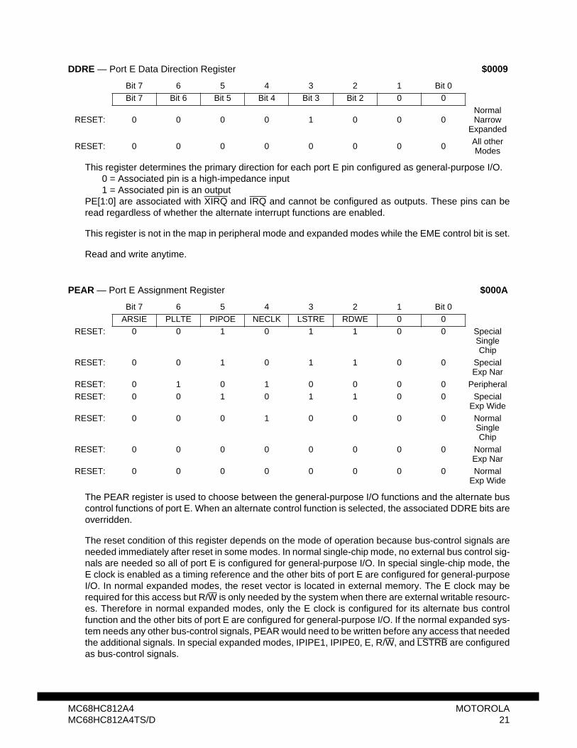
This register determines the primary direction for each port E pin configured as general-purpose I/O.0 = Associated pin is a high-impedance input1 = Associated pin is an output
PE[1:0] are associated with XIRQ and IRQ and cannot be configured as outputs. These pins can beread regardless of whether the alternate interrupt functions are enabled.
This register is not in the map in peripheral mode and expanded modes while the EME control bit is set.
Read and write anytime.
The PEAR register is used to choose between the general-purpose I/O functions and the alternate buscontrol functions of port E. When an alternate control function is selected, the associated DDRE bits areoverridden.
The reset condition of this register depends on the mode of operation because bus-control signals areneeded immediately after reset in some modes. In normal single-chip mode, no external bus control sig-nals are needed so all of port E is configured for general-purpose I/O. In special single-chip mode, theE clock is enabled as a timing reference and the other bits of port E are configured for general-purposeI/O. In normal expanded modes, the reset vector is located in external memory. The E clock may berequired for this access but R/W is only needed by the system when there are external writable resourc-es. Therefore in normal expanded modes, only the E clock is configured for its alternate bus controlfunction and the other bits of port E are configured for general-purpose I/O. If the normal expanded sys-tem needs any other bus-control signals, PEAR would need to be written before any access that neededthe additional signals. In special expanded modes, IPIPE1, IPIPE0, E, R/W, and LSTRB are configuredas bus-control signals.
DDRE — Port E Data Direction Register $0009
Bit 7 6 5 4 3 2 1 Bit 0Bit 7 Bit 6 Bit 5 Bit 4 Bit 3 Bit 2 0 0
RESET: 0 0 0 0 1 0 0 0Normal Narrow
Expanded
RESET: 0 0 0 0 0 0 0 0 All other Modes
PEAR — Port E Assignment Register $000A
Bit 7 6 5 4 3 2 1 Bit 0ARSIE PLLTE PIPOE NECLK LSTRE RDWE 0 0
RESET: 0 0 1 0 1 1 0 0 Special Single Chip
RESET: 0 0 1 0 1 1 0 0 Special Exp Nar
RESET: 0 1 0 1 0 0 0 0 PeripheralRESET: 0 0 1 0 1 1 0 0 Special
Exp WideRESET: 0 0 0 1 0 0 0 0 Normal
Single Chip
RESET: 0 0 0 0 0 0 0 0 Normal Exp Nar
RESET: 0 0 0 0 0 0 0 0 Normal Exp Wide
MC68HC812A4 MOTOROLAMC68HC812A4TS/D 21

In peripheral mode, the PEAR register is not accessible for reads or writes. However, the PLLTE controlbit is reset to one to configure PE6 as a test output from the PLL module.
ARSIE — Auxiliary Reset Input EnableRead and write anytime.
0 = PE7 is general-purpose I/O.1 = PE7 is a high-true reset input. Reset timing is the same as that of the low-true RESET pin.
PLLTE — PLL Testing EnableNormal: write never; Special: write anytime EXCEPT the first time. Read anytime.
0 = PE6 is general-purpose I/O or pipe output.1 = PE6 is a test signal output from the PLL module (no effect in single chip or normal expanded
modes). PIPOE = 1 overrides this function and forces PE6 to be a pipe status output signal.
PIPOE — Pipe Status Signal Output EnableNormal: write once; Special: write anytime except the first time. Read anytime.
0 = PE[6:5] are general-purpose I/O (if PLLTE = 1, PE6 is a test output signal from the PLL module).1 = PE[6:5] are outputs and indicate the state of the instruction queue (no effect in single chip
modes).
NECLK — No External E ClockNormal: write anytime; Special: write never. Read anytime. In peripheral mode, E is an input and in allother modes, E is an output.
0 = PE4 is the external E-clock pin. To get a free-running E clock in single-chip modes, useNECLK=0 and IVIS=1. A 16-bit write to PEAR:MODE can configure these bits in one operation.
1 = PE4 is a general-purpose I/O pin.
LSTRE — Low Strobe (LSTRB) EnableNormal: write once; Special: write anytime except the first time. Read anytime. This bit has no effect insingle-chip modes or normal expanded narrow mode.
0 = PE3 is a general-purpose I/O pin.1 = PE3 is configured as the LSTRB bus-control output, provided the MCU is not in single chip or
normal expanded narrow modes.LSTRB is used during external writes. After reset in normal expanded mode, LSTRB is disabled. Ifneeded, it should be enabled before external writes. External reads do not normally need LSTRB be-cause all 16 data bits can be driven even if the MCU only needs eight bits of data.
In normal expanded narrow mode this pin is reset to an output driving high allowing the pin to be anoutput while in and immediately after reset.
RDWE — Read/Write EnableNormal: write once; Special: write anytime except the first time. Read anytime. This bit has no effect insingle-chip modes.
0 = PE2 is a general-purpose I/O pin.1 = PE2 is configured as the R/W pin. In single chip modes, RDWE has no effect and PE2 is a gen-
eral-purpose I/O pin.R/W is used for external writes. After reset in normal expanded mode, it is disabled. If needed it shouldbe enabled before any external writes.
MOTOROLA MC68HC812A422 MC68HC812A4TS/D

These bits select pull-up resistors for any pin in the corresponding port that is currently configured asan input. This register is not in the map in peripheral mode.
Read and write anytime.
PUPH — Pull-Up Port H Enable0 = Port H pull-ups are disabled.1 = Enable pull-up devices for all port H input pins.
PUPG — Pull-Up Port G Enable0 = Port G pull-ups are disabled.1 = Enable pull-up devices for all port G input pins.
PUPF — Pull-Up Port F Enable0 = Port F pull-ups are disabled.1 = Enable pull-up devices for all port F input pins.
PUPE — Pull-Up Port E Enable0 = Port E pull-ups on PE3, PE2, and PE0 are disabled.1 = Enable pull-up devices for port E input pins PE3, PE2, and PE0.
PUPD — Pull-Up Port D Enable0 = Port D pull-ups are disabled.1 = Enable pull-up devices for all port D input pins.
This bit has no effect if port D is being used as part of the data bus (the pull-ups are inactive).
PUPC — Pull-Up Port C Enable0 = Port C pull-ups are disabled.1 = Enable pull-up devices for all port C input pins.
This bit has no effect if port C is being used as part of the data bus (the pull-ups are inactive).
PUPB — Pull-Up Port B Enable0 = Port B pull-ups are disabled.1 = Enable pull-up devices for all port B input pins.
This bit has no effect if port B is being used as part of the address bus (the pull-ups are inactive).
PUPA — Pull-Up Port A Enable0 = Port A pull-ups are disabled.1 = Enable pull-up devices for all port A input pins.
This bit has no effect if port A is being used as part of the address bus (the pull-ups are inactive).
PUCR — Pull Up Control Register $000C
Bit 7 6 5 4 3 2 1 Bit 0PUPH PUPG PUPF PUPE PUPD PUPC PUPB PUPA
RESET: 1 1 1 1 1 1 1 1
MC68HC812A4 MOTOROLAMC68HC812A4TS/D 23

These bits select reduced drive for the associated port pins. This gives reduced power consumption andreduced RFI with a slight increase in transition time (depending on loading). The reduced drive functionis independent of which function is being used on a particular port.
This register is not in the map in peripheral mode.
Normal: write anytime; Special: write never. Read anytime.
RDPJ — Reduced Drive of Port J0 = All port J output pins have full drive enabled.1 = All port J output pins have reduced drive capability.
RDPH — Reduced Drive of Port H0 = All port H output pins have full drive enabled.1 = All port H output pins have reduced drive capability.
RDPG — Reduced Drive of Port G0 = All port G output pins have full drive enabled.1 = All port G output pins have reduced drive capability.
RDPF — Reduced Drive of Port F0 = All port F output pins have full drive enabled.1 = All port F output pins have reduced drive capability.
RDPE — Reduced Drive of Port E0 = All port E output pins have full drive enabled.1 = All port E output pins have reduced drive capability.
RDPD — Reduced Drive of Port D0 = All port D output pins have full drive enabled.1 = All port D output pins have reduced drive capability.
RDPC — Reduced Drive of Port C0 = All port C output pins have full drive enabled.1 = All port C output pins have reduced drive capability.
RDPAB — Reduced Drive of Port A and Port B0 = All port A and port B output pins have full drive enabled.1 = All port A and port B output pins have reduced drive capability.
RDRIV — Reduced Drive of I/O Lines $000D
Bit 7 6 5 4 3 2 1 Bit 0RDPJ RDPH RDPG RDPF RDPE RDPD RDPC RDPAB
RESET: 0 0 0 0 0 0 0 0
MOTOROLA MC68HC812A424 MC68HC812A4TS/D

6 Operating Modes and Resource MappingEight possible operating modes determine the operating configuration of the MC68HC812A4. Eachmode has an associated default memory map and external bus configuration. After reset, most systemresources can be mapped to other addresses by writing to the appropriate control registers.
6.1 Operating Modes
The operating mode out of reset is determined by the states of the BKGD, MODB, and MODA pins dur-ing reset.
The SMODN, MODB, and MODA bits in the MODE register show current operating mode and providelimited mode switching during operation. The states of the BKGD, MODB, and MODA pins are latchedinto these bits on the rising edge of the reset signal.
There are two basic types of operating modes:
Normal modes — some registers and bits are protected against accidentalchanges.
Special modes — allow greater access to protected control registers and bitsfor special purposes such as testing and emulation.
A system development and debug feature, background debug mode (BDM), is available in all modes.In special single-chip mode, BDM is active immediately after reset.
6.1.1 Normal Operating Modes
These modes provide three operating configurations. Background debugging is available in all threemodes, but must first be enabled for some operations by means of a BDM command. BDM can then bemade active by another BDM command.
Normal Expanded Wide Mode — This is a normal mode of operation in which theexpanded bus is present with a 16-bit data bus. Ports A and B are used for the 16-bit address bus. Ports C and D are used for the 16-bit data bus.
Normal Expanded Narrow Mod e — This is a normal mode of operation in whichthe expanded bus is present with an 8-bit data bus. Ports A and B are used forthe16-bit address bus. Port C is used as the data bus. In this mode, 16-bit data ispresented one byte at a time, the high byte followed by the low byte. The addressis automatically incremented on the second cycle.
Normal Single-Chip Mode — There are no external address and data buses inthis mode. The MCU operates as a stand-alone device and all program and dataresources are on-chip. External port pins normally associated with address anddata buses can be used for general-purpose I/O.
Table 9 Mode Selection
BKGD MODB MODA ModePort APort B
Port C Port D
0 0 0 Special Single Chip G.P. I/O G.P. I/O G.P. I/O0 0 1 Special Expanded Narrow ADDR DATA G.P. I/O0 1 0 Special Peripheral ADDR DATA DATA0 1 1 Special Expanded Wide ADDR DATA DATA1 0 0 Normal Single Chip G.P. I/O G.P. I/O G.P. I/O1 0 1 Normal Expanded Narrow ADDR DATA G.P. I/O1 1 0 Reserved (Forced to Peripheral) — — —1 1 1 Normal Expanded Wide ADDR DATA DATA
MC68HC812A4 MOTOROLAMC68HC812A4TS/D 25

6.1.2 Special Operating Modes
There are three special operating modes that correspond to normal operating modes. These operatingmodes are commonly used in factory testing and system development. In addition, there is a specialperipheral mode, in which an external master, such as an I.C. tester, can control the on-chip peripher-als.
Special Expanded Wide Mode — This mode can be used for emulation of normalexpanded wide mode and emulation of normal single-chip mode. Port A and portB are used for a 16-bit address bus. Port C and port D are used for a 16-bit databus.
Special Expanded Narrow Mode — This mode can be used for emulation of nor-mal expanded narrow mode. Port A and port B are used for the 16-bit address bus.Port C is used as the data bus. In this mode external 16-bit data is handled as twoback-to-back bus cycles, one for the high byte followed by one for the low byte. Fordevelopment purposes, port D can be made available for visibility of 16-bit internalaccesses by setting the EMD and IVIS control bits.
Special Single-Chip Mode — This mode can be used to force the MCU to activeBDM mode to allow system debug through the BKGD pin. There are no externaladdress and data buses in this mode. The MCU operates as a stand-alone deviceand all program and data space are on-chip. External port pins can be used forgeneral-purpose I/O.
Special Peripheral Mode — The CPU is not active in this mode. An external mas-ter can control on-chip peripherals for testing purposes. It is not possible to changeto or from this mode without going through reset. Background debugging shouldnot be used while the MCU is in special peripheral mode as internal bus conflictsbetween BDM and the external master can cause improper operation of bothmodes.
6.2 Background Debug Mode
Background debug mode (BDM) is an auxiliary operating mode that is used for system development.BDM is implemented in on-chip hardware and provides a full set of debug operations. Some BDM com-mands can be executed while the CPU is operating normally. Other BDM commands are firmwarebased, and require the BDM firmware to be enabled and active for execution.
In special single-chip mode, BDM is enabled and active immediately out of reset. BDM is available inall other operating modes, but must be enabled before it can be activated. BDM should not be used inspecial peripheral mode because of potential bus conflicts.
Once enabled, background mode can be made active by a serial command sent via the BKGD pin orexecution of a CPU12 BGND instruction. While background mode is active, the CPU can interpret spe-cial debugging commands, and read and write CPU registers, peripheral registers, and locations inmemory.
While BDM is active, the CPU executes code located in a small on-chip ROM mapped to addresses$FF20 to $FFFF, and BDM control registers are accessible at addresses $FF00 to $FF06. The BDMROM replaces the regular system vectors while BDM is active. While BDM is active, the user memoryfrom $FF00 to $FFFF is not in the map except through serial BDM commands.
MOTOROLA MC68HC812A426 MC68HC812A4TS/D

MODE controls the MCU operating mode and various configuration options. This register is not in themap in peripheral mode
SMODN, MODB, MODA — Mode Select Special, B and A These bits show the current operating mode and reflect the status of the BKGD, MODB and MODA inputpins at the rising edge of reset.
Read anytime. SMODN may only be written if SMODN = 0 (in special modes) but the first write is ig-nored; MODB, MODA may be written once if SMODN = 1; anytime if SMODN = 0, except that specialperipheral and reserved modes cannot be selected.
ESTR — E Clock Stretch EnableDetermines if the E Clock behaves as a simple free-running clock or as a bus control signal that is activeonly for external bus cycles.
0 = E never stretches (always free running).1 = E stretches high during external access cycles and low during non-visible internal accesses.
Normal modes: write once; Special modes: write anytime, read anytime.
IVIS — Internal VisibilityThis bit determines whether internal ADDR, DATA, R/W and LSTRB signals can be seen on the exter-nal bus during accesses to internal locations. In special narrow mode if this bit is set and EMD = 1 whenan internal access occurs, the data appears wide on port C and port D. This allows for emulation. Visi-bility is not available when the part is operating in a single-chip mode.
0 = No visibility of internal bus operations on external bus. 1 = Internal bus operations are visible on external bus.
Normal modes: write once; Special modes: write anytime EXCEPT the first time. Read anytime.
MODE — Mode Register $000B
Bit 7 6 5 4 3 2 1 Bit 0SMODN MODB MODA ESTR IVIS 0 EMD EME
RESET: 0 0 0 1 1 0 1 1 Special Single Chip
RESET: 0 0 1 1 1 0 1 1 Special Exp Nar
RESET: 0 1 0 1 1 0 1 1 PeripheralRESET: 0 1 1 1 1 0 1 1 Special
Exp WideRESET: 1 0 0 1 0 0 0 0 Normal
Single Chip
RESET: 1 0 1 1 0 0 0 0 Normal Exp Nar
RESET: 1 1 1 1 0 0 0 0 Normal Exp Wide
MC68HC812A4 MOTOROLAMC68HC812A4TS/D 27

EMD — Emulate Port DThis bit only has meaning in special expanded narrow mode.
In expanded wide modes and special peripheral mode, PORTD, DDRD, KWIED and KWIFD are re-moved from the memory map regardless of the state of this bit.
In single-chip modes and normal expanded narrow mode, PORTD, DDRD, KWIED and KWIFD are inthe memory map regardless of the state of this bit.
0 = PORTD, DDRD, KWIED and KWIFD are in the memory map.1 = If in special expanded narrow mode; PORTD, DDRD, KWIED and KWIFD are removed from
the memory map. Removing the registers from the map allows the user to emulate the functionof these registers externally.
Normal modes: write once; Special modes: write anytime EXCEPT the first time. Read anytime.
EME — Emulate Port EIn single-chip mode PORTE and DDRE are always in the map regardless of the state of this bit.
0 = PORTE and DDRE are in the memory map. 1 = If in an expanded mode, PORTE and DDRE are removed from the internal memory map. Re-
moving the registers from the map allows the user to emulate the function of these registersexternally.
Normal modes: write once; special modes: write anytime EXCEPT the first time. Read anytime.
6.3 Internal Resource Mapping
The internal register block, RAM, and EEPROM have default locations within the 64-Kbyte standard ad-dress space but may be reassigned to other locations during program execution by setting bits in map-ping registers INITRG, INITRM, and INITEE. During normal operating modes these registers can bewritten once. It is advisable to explicitly establish these resource locations during the initialization phaseof program execution, even if default values are chosen, in order to protect the registers from inadvert-ent modification later.
Writes to the mapping registers go into effect between the cycle that follows the write and the cycle afterthat. To assure that there are no unintended operations, a write to one of these registers should be fol-lowed with a NOP instruction.
If conflicts occur when mapping resources, the register block will take precedence over the other re-sources; RAM or EEPROM addresses occupied by the register block will not be available for storage.When active, BDM ROM takes precedence over other resources although a conflict between BDMROM and register space is not possible. Table 10 shows resource mapping precedence.
All address space not utilized by internal resources is, by default, external memory. The memory ex-pansion module manages three memory overlay windows: program, data, and one extra page overlay.The size and location of the program and data overlay windows are fixed. One of two locations can beselected for the extra page (EPAGE).
Table 10 Mapping Precedence
Precedence Resource1 BDM ROM (if active)2 Register Space3 RAM4 EEPROM5 External Memory
MOTOROLA MC68HC812A428 MC68HC812A4TS/D

6.3.1 Register Block Mapping
After reset the 512 byte register block resides at location $0000 but can be reassigned to any 2-Kbyteboundary within the standard 64-Kbyte address space. Mapping of internal registers is controlled by fivebits in the INITRG register. The register block occupies the first 512 bytes of the 2-Kbyte block.
REG[15:11] — Internal register map position These bits specify the upper five bits of the 16-bit registers address.
Normal modes: write once; special modes: write anytime. Read anytime.
6.3.2 RAM Mapping
The MC68HC812A4 has 1 Kbyte of fully static RAM that is used for storing instructions, variables, andtemporary data during program execution. After reset, RAM addressing begins at location $0800 butcan be assigned to any 2-Kbyte boundary within the standard 64-Kbyte address space. Mapping of in-ternal RAM is controlled by five bits in the INITRM register. The RAM array occupies the last 1 Kbyte ofthe 2-Kbyte block.
RAM[15:11] — Internal RAM map position These bits specify the upper five bits of the 16-bit RAM address.
Normal modes: write once; special modes: write anytime. Read anytime.
6.3.3 EEPROM Mapping
The MC68HC812A4 has 4 Kbytes of EEPROM which is activated by the EEON bit in the INITEE regis-ter.
Mapping of internal EEPROM is controlled by four bits in the INITEE register. After reset EEPROM ad-dress space begins at location $1000 but can be mapped to any 4-Kbyte boundary within the standard64-Kbyte address space.
INITRG — Initialization of Internal Register Position Register $0011
Bit 7 6 5 4 3 2 1 Bit 0REG15 REG14 REG13 REG12 REG11 0 0 0
RESET: 0 0 0 0 0 0 0 0
INITRM — Initialization of Internal RAM Position Register $0010
Bit 7 6 5 4 3 2 1 Bit 0RAM15 RAM14 RAM13 RAM12 RAM11 0 0 0
RESET: 0 0 0 0 1 0 0 0
INITEE— Initialization of Internal EEPROM Position Register $0012
Bit 7 6 5 4 3 2 1 Bit 0EE15 EE14 EE13 EE12 0 0 0 EEON
RESET: 0 0 0 1 0 0 0 1 Expand & Peripheral
RESET: 1 1 1 1 0 0 0 1 Single Chip
MC68HC812A4 MOTOROLAMC68HC812A4TS/D 29
EE[15:12] — Internal EEPROM map position These bits specify the upper four bits of the 16-bit EEPROM address.
Normal modes: write once; special modes: write anytime. Read anytime.
EEON — internal EEPROM On (Enabled)This bit is forced to one in single-chip modes.
Read or write anytime.0 = Removes the EEPROM from the map. 1 = Places the on-chip EEPROM in the memory map at the address selected by EE[15:12].
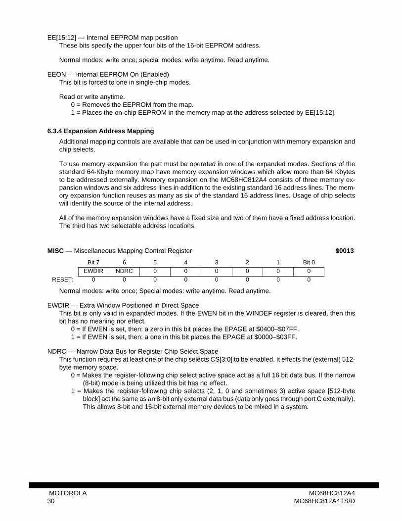
6.3.4 Expansion Address Mapping
Additional mapping controls are available that can be used in conjunction with memory expansion andchip selects.
To use memory expansion the part must be operated in one of the expanded modes. Sections of thestandard 64-Kbyte memory map have memory expansion windows which allow more than 64 Kbytesto be addressed externally. Memory expansion on the MC68HC812A4 consists of three memory ex-pansion windows and six address lines in addition to the existing standard 16 address lines. The mem-ory expansion function reuses as many as six of the standard 16 address lines. Usage of chip selectswill identify the source of the internal address.
All of the memory expansion windows have a fixed size and two of them have a fixed address location.The third has two selectable address locations.
Normal modes: write once; Special modes: write anytime. Read anytime.
EWDIR — Extra Window Positioned in Direct SpaceThis bit is only valid in expanded modes. If the EWEN bit in the WINDEF register is cleared, then thisbit has no meaning nor effect.
0 = If EWEN is set, then: a zero in this bit places the EPAGE at $0400–$07FF.1 = If EWEN is set, then: a one in this bit places the EPAGE at $0000–$03FF.
NDRC — Narrow Data Bus for Register Chip Select SpaceThis function requires at least one of the chip selects CS[3:0] to be enabled. It effects the (external) 512-byte memory space.
0 = Makes the register-following chip select active space act as a full 16 bit data bus. If the narrow(8-bit) mode is being utilized this bit has no effect.
1 = Makes the register-following chip selects (2, 1, 0 and sometimes 3) active space [512-byteblock] act the same as an 8-bit only external data bus (data only goes through port C externally).This allows 8-bit and 16-bit external memory devices to be mixed in a system.
MISC — Miscellaneous Mapping Control Register $0013
Bit 7 6 5 4 3 2 1 Bit 0EWDIR NDRC 0 0 0 0 0 0
RESET: 0 0 0 0 0 0 0 0
MOTOROLA MC68HC812A430 MC68HC812A4TS/D

6.4 Memory Maps
The following diagrams illustrate the memory map for each mode of operation immediately after reset.
Figure 4 MC68HC812A4 Memory Map
REGISTERS(MAPPABLE TO ANY 2K SPACE)
$01FF
RAM(MAPPABLE TO ANY 2K SPACE)
EXPANDED SINGLE CHIPNORMAL
SINGLE CHIPSPECIAL
EXT
EXT
$0BFF
$FFFF
$F000
EEPROM(MAPPABLE TO ANY 4K SPACE)
$1000
$1FFF
EXT
VECTORS VECTORS
VECTORS
VECTORS
BDM(if active)
EEPROM(Single-Chip Mode
$FFFF
$0000
$0800
$FFFF
$FF00
$FF00
$F000
$1000
$0000
$0800
$2000
$FFC0
HC812A4 MEM MAP
MC68HC812A4 MOTOROLAMC68HC812A4TS/D 31

7 EEPROMThe MC68HC812A4 EEPROM serves as a 4096-byte nonvolatile memory which can be used for fre-quently accessed static data or as fast access program code. Operating system kernels and standardsubroutines would benefit from this feature.
The MC68HC812A4 EEPROM is arranged in a 16-bit configuration. The EEPROM array may be readas either bytes, aligned words or misaligned words. Access times is one bus cycle for byte and alignedword access and two bus cycles for misaligned word operations.
Programming is by byte or aligned word. Attempts to program or erase misaligned words will fail. Onlythe lower byte will be latched and programmed or erased. Programming and erasing of the user EE-PROM can be done in all modes.
Each EEPROM byte or aligned word must be erased before programming. The EEPROM module sup-ports byte, aligned word, row (32 bytes) or bulk erase, all using the internal charge pump. Bulk erasureof odd and even rows is also possible in test modes; the erased state is $FF. The EEPROM modulehas hardware interlocks which protect stored data from corruption by accidentally enabling the program/erase voltage. Programming voltage is derived from the internal VDD supply with an internal chargepump. The EEPROM has a minimum program/erase life of 10,000 cycles over the complete operatingtemperature range.
7.1 EEPROM Programmer’s Model
The EEPROM module consists of two separately addressable sections. The first is a four-byte memorymapped control register block used for control, testing and configuration of the EEPROM array. Thesecond section is the EEPROM array itself.
At reset, the four-byte register section starts at address $00F0 and the EEPROM array is located fromaddresses $1000 to $1FFF (see Figure 5 ). For information on remapping the register block and EE-PROM address space, refer to 6 Operating Modes and Resource Mapping .
Read/write access to the memory array section can be enabled or disabled by the EEON control bit inthe INITEE register. This feature allows the access of memory mapped resources that have lower pri-ority than the EEPROM memory array. EEPROM control registers can be accessed and EEPROM lo-cations may be programmed or erased regardless of the state of EEON.
Using the normal EEPROG control, it is possible to continue program/erase operations during WAIT.For lowest power consumption during WAIT, stop program/erase by turning off EEPGM.
If the STOP mode is entered during programming or erasing, program/erase voltage will be automati-cally turned off and the RC clock (if enabled) is stopped. However, the EEPGM control bit will remainset. When STOP mode is terminated, the program/erase voltage will be automatically turned back on ifEEPGM is set.
At low bus frequencies, the RC clock must be turned on for program/erase.
MOTOROLA MC68HC812A432 MC68HC812A4TS/D

Figure 5 EEPROM Block Protect Mapping
7.2 EEPROM Control Registers
EESWAI — EEPROM Stops in Wait Mode0 = Module is not affected during wait mode1 = Module ceases to be clocked during wait mode
This bit should be cleared if the wait mode vectors are mapped in the EEPROM array.
PROTLCK — Block Protect Write Lock0 = Block protect bits and bulk erase protection bit can be written1 = Block protect bits are locked
Read anytime. Write once in normal modes (SMODN = 1), set and clear any time in special modes(SMODN = 0).
EERC — EEPROM Charge Pump Clock0 = System clock is used as clock source for the internal charge pump. Internal RC oscillator is
stopped.1 = Internal RC oscillator drives the charge pump. The RC oscillator is required when the system
bus clock is lower than fPROG.Read and write anytime.
Prevents accidental writes to EEPROM. Read anytime. Write anytime if EEPGM = 0 and PROTLCK = 0.
EEMCR — EEPROM Module Configuration $00F0
Bit 7 6 5 4 3 2 1 Bit 01 1 1 1 1 EESWAI PROTLCK EERC
RESET: 1 1 1 1 1 1 0 0
EEPROT — EEPROM Block Protect $00F1
Bit 7 6 5 4 3 2 1 Bit 01 BPROT6 BPROT5 BPROT4 BPROT3 BPROT2 BPROT1 BPROT0
RESET: 1 1 1 1 1 1 1 1
BPROT6 2 KBYTES
BPROT51 KBYTE
BPROT4 — 512 BYTES
BPROT3 — 256 BYTESBPROT2 — 128 BYTESBPROT1 — 64 BYTESBPROT0 — 64 BYTES
RESERVED (64 BYTES)
VECTORS (64 BYTES)
$_000
$_800
$_C00
$_E00$_F00$_F80$_FC0$_FFF
$FF80
$FFBF$FFC0
$FFFF
SINGLE CHIP VECTORS
HC812A4 EEPROM BLOCK PROT
MC68HC812A4 MOTOROLAMC68HC812A4TS/D 33

BPROT[6:0] — EEPROM Block Protection0 = Associated EEPROM block can be programmed and erased.1 = Associated EEPROM block is protected from being programmed and erased.
Cannot be modified while programming is taking place (EEPGM = 1).
Read anytime. Write in special modes only (SMODN = 0). These bits are used for test purposes only.In normal modes the bits are forced to zero.
EEODD — Odd Row Programming0 = Odd row bulk programming/erasing is disabled.1 = Bulk program/erase all odd rows.
EEVEN — Even Row Programming0 = Even row bulk programming/erasing is disabled.1 = Bulk program/erase all even rows.
MARG — Program and Erase Voltage Margin Test Enable0 = Normal operation.1 = Program and Erase Margin test.
This bit is used to evaluate the program/erase voltage margin.
EECPD — Charge Pump Disable0 = Charge pump is turned on during program/erase.1 = Disable charge pump.
EECPRD — Charge Pump Ramp DisableKnown to enhance write/erase endurance of EEPROM cells.
0 = Charge pump is turned on progressively during program/erase.1 = Disable charge pump controlled ramp up.
ECPM — Charge Pump Monitor Enable0 = Normal operation.1 = Output the charge pump voltage on the IRQ/VPP pin.
Table 11 4-Kbyte EEPROM Block Protection
Bit Name Block Protected Block SizeBPROT6 $1000 to $17FF 2048 BytesBPROT5 $1800 to $1BFF 1024 BytesBPROT4 $1C00 to $1DFF 512 BytesBPROT3 $1E00 to $1EFF 256 BytesBPROT2 $1F00 to $1F7F 128 BytesBPROT1 $1F80 to $1FBF 64 BytesBPROT0 $1FC0 to $1FFF 64 Bytes
EETST — EEPROM Test $00F2
Bit 7 6 5 4 3 2 1 Bit 0EEODD EEVEN MARG EECPD EECPRD 0 EECPM 0
RESET: 0 0 0 0 0 0 0 0
EEPROG — EEPROM Control $00F3
Bit 7 6 5 4 3 2 1 Bit 0BULKP 0 0 BYTE ROW ERASE EELAT EEPGM
RESET: 1 0 0 0 0 0 0 0
MOTOROLA MC68HC812A434 MC68HC812A4TS/D

BULKP — Bulk Erase Protection0 = EEPROM can be bulk erased.1 = EEPROM is protected from being bulk or row erased.
Read anytime. Write anytime if EEPGM = 0 and PROTLCK = 0.
BYTE — Byte and Aligned Word Erase0 = Bulk or row erase is enabled.1 = One byte or one aligned word erase only.
Read anytime. Write anytime if EEPGM = 0.
ROW — Row or Bulk Erase (when BYTE = 0)0 = Erase entire EEPROM array.1 = Erase only one 32-byte row.
Read anytime. Write anytime if EEPGM = 0.
BYTE and ROW have no effect when ERASE = 0
If BYTE = 1 and test mode is not enabled, only the location specified by the address written to the pro-gramming latches will be erased. The operation will be a byte or an aligned word erase depending onthe size of written data.
ERASE — Erase Control0 = EEPROM configuration for programming.1 = EEPROM configuration for erasure.
Read anytime. Write anytime if EEPGM = 0.
Configures the EEPROM for erasure or programming.
EELAT — EEPROM Latch Control0 = EEPROM set up for normal reads.1 = EEPROM address and data bus latches set up for programming or erasing.
Read anytime. Write anytime if EEPGM = 0.
NOTEWhen EELAT is set, the entire EEPROM is unavailable for reads; therefore, no pro-gram residing in the EEPROM can be executed while attempting to program un-used EEPROM space. Care should be taken that no references to the EEPROMare used while programming. Interrupts should be turned off if the vectors are inthe EEPROM. Timing and any serial communications must be done with pollingduring the programming process.
BYTE, ROW, ERASE and EELAT bits can be written simultaneously or in any sequence.
EEPGM — Program and Erase Enable0 = Disables program/erase voltage to EEPROM.1 = Applies program/erase voltage to EEPROM.
The EEPGM bit can be set only after EELAT has been set. When EELAT and EEPGM are set simulta-neously, EEPGM remains clear but EELAT is set.
The BULKP, BYTE, ROW, ERASE and EELAT bits cannot be changed when EEPGM is set. To com-plete a program or erase, two successive writes to clear EEPGM and EELAT bits are required beforereading the programmed data. A write to an EEPROM location has no effect when EEPGM is set.
Table 12 Erase Selection
Byte Row Block Size0 0 Bulk erase entire EEPROM array0 1 Row erase 32 bytes1 0 Byte or aligned word erase1 1 Byte or aligned word erase
MC68HC812A4 MOTOROLAMC68HC812A4TS/D 35

Latched address and data cannot be modified during program or erase.
A program or erase operation should follow the sequence below:
1. Write BYTE, ROW and ERASE to the desired value, write EELAT = 12. Write a byte or an aligned word to an EEPROM address3. Write EEPGM = 14. Wait for programming (tPROG) or erase (terase) delay time5. Write EEPGM = 06. Write EELAT = 0
It is possible to program/erase more bytes or words without intermediate EEPROM reads by jumpingfrom step 5 to step 2.
MOTOROLA MC68HC812A436 MC68HC812A4TS/D

8 Memory Expansion and Chip Select
8.1 General Description of Memory Expansion
To use memory expansion the MC68HC812A4 must be operated in one of the expanded modes. Sec-tions of the standard 64-Kbyte address space have memory expansion windows which allow an exter-nal address space larger than 64-Kbytes. Memory expansion consists of three memory expansionwindows and six address lines which are used in addition to the standard 16 address lines.
The memory expansion function reuses as many as six of the standard 16 address lines. To do this,some of the upper address lines of internal addresses falling in an active window are overridden. Con-sequently, the address viewed externally may not match the internal address. Usage of chip selects willidentify the source of the internal address for debugging and selection of the proper external devices.
All memory expansion windows have a fixed size and two have a fixed address location. The third hastwo selectable address locations. When an internal address falls into one of these active windows it istranslated as shown in the table.
Addresses ADDR[9:0] are not affected by memory expansion and are the same externally as they areinternally. Addresses ADDR[21:16] are only generated by memory expansion and are individually en-abled by software programmable control bits. If not enabled they may be used as general-purpose I/O.Addresses ADDR[15:10] can be the internal addresses or they can be modified by the memory expan-sion module. These are not available as general-purpose I/O in expanded modes.
8.2 Generation of Chip Selects
To use chip selects the MC68HC812A4 must be in one of the expanded modes. Each of the seven chipselects has an address space for which it is active — that is, when the current CPU address is in therange of that chip select it becomes active. Chip selects are generally used to reduce or eliminate ex-ternal address decode logic. These active low signals usually are connected directly to the chip selectpin of an external device.
1. The EWDIR bit in the MISC register selects the E window address (1 = $0000 to $03FF including direct space, 0 = $0400 to$07FF).
Table 13 Memory Expansion Values (All Port G Assigned to Memory Expansion)
Internal Address A21 A20 A19 A18 A17 A16 A15 A14 A13 A12 A11 A10
$0000–$03FFEWDIR1=1, EWEN
=1
1 1 1 1 PEA17 PEA16 PEA15 PEA14 PEA13 PEA12 PEA11 PEA10
$0000–$03FFEWDIR OR EWEN =0
1 1 1 1 1 1 A15 A14 A13 A12 A11 A10
$0400–$07FFEWDIR =0, EWEN =1
1 1 1 1 PEA17 PEA16 PEA15 PEA14 PEA13 PEA12 PEA11 PEA10
$0400–$07FFEWDIR =1, EWEN =x
OREWDIR =x, EWEN =0
1 1 1 1 1 1 A15 A14 A13 A12 A11 A10
$0800–$6FFF 1 1 1 1 1 1 A15 A14 A13 A12 A11 A10
$7000–$7FFFDWEN = 1
1 1 PDA19 PDA18 PDA17 PDA16 PDA15 PDA14 PDA13 PDA12 A11 A10
$7000–$7FFFDWEN = 0
1 1 1 1 1 1 A15 A14 A13 A12 A11 A10
$8000–$BFFFPWEN = 1
PPA21 PPA20 PPA19 PPA18 PPA17 PPA16 PPA15 PPA14 A13 A12 A11 A10
$8000–$BFFFPWEN = 0
1 1 1 1 1 1 A15 A14 A13 A12 A11 A10
$C000–$FFFF 1 1 1 1 1 1 A15 A14 A13 A12 A11 A10
MC68HC812A4 MOTOROLAMC68HC812A4TS/D 37
8.2.1 Chip Selects Independent of Memory Expansion
Three types of chip selects on the MC68HC812A4 are program memory chip selects, other memorychip selects and peripheral chip selects. Memory chip selects cover a medium to large address space.Peripheral chip selects (CS[3:0]) cover a small address space. The program memory chip select in-cludes the vector space and is generally used with non-volatile memory. To start the user’s program,the program chip select is designed to be active out of reset. This is the only chip select which has afunctional difference from the others, so a small memory could use a peripheral chip select and a pe-ripheral could use a memory chip select.
Figure 6 shows peripheral chip selects in an expanded portion of the memory map. Chip selectsCS[2:0] always map to the same 2-Kbyte block as the internal register space. The internal registers cov-er the first 512 bytes and these chip selects cover all or part of the 512 bytes following the register spaceblocking out a full 1-Kbyte space. CS3 can map with these other chip selects or be used in a 1-Kbytespace by itself which starts at either $0000 or $0400. CS3 can only be used for a 1-Kbyte space whenit selects the E Page of memory expansion and E Page is active.
CS3 can be used with a 1-Kbyte space in systems not using memory expansion. However, it must bemade to appear like memory expansion is in use. One of many possible configurations is the following:
• Select the desired 1-Kbyte space for EPAGE (EWDIR in MISC in the MMI)• Write the EPAGE register with $0000 if EWDIR is one or $0001 if EWDIR is zero• Designate all port G pins as I/O• Enable EPAGE and CS3• Make CS3 follow EPAGE
MOTOROLA MC68HC812A438 MC68HC812A4TS/D

Figure 6 Chip Selects [3:0] (Partial Memory Map)
Register Value Meaning
INITRM $00 Assigns internal RAM to $0000–$0FFF
INITRG $08 Assigns register block to $0800–$09FF and register-following chip selects at $0A00–$0B
WINDEF $20 Enable EPAGE
MXAR $00 No port G lines assigned as extended address
CSCTL0 $xF Enables CS3, CS2, CS1, and CS0
CSCTL1 $x8 Makes CS3 follow EPAGE
MISC %0xxxxxxx Puts EPAGE at $0400–$07FF
EPAGE $01 Keeps the translated value of the upper addresses the same as it would have been befortranslation; not necessary if all external devices use chip selects.
$0000
$0100
$0200
$0300
$0400
$0500
$0600
$0700
$0800
$0900
$0A00
$0B00
$0C00
$0D00
$0E00
$0F00
$0FFF
INTERNAL SPACE
RAM1 KBYTE
REGISTERS
EXTERNAL SPACE
CS0
CS1
256 BYTES
128 BYTES
128 BYTES
1 KBYTECS3
CS2
HC812A4 CHIP SEL PART
MC68HC812A4 MOTOROLAMC68HC812A4TS/D 39

8.2.2 Chip Selects Used in Conjunction with Memory Expansion
Memory expansion and chip select functions can work independently, but systems requiring memoryexpansion perform better when chip selects are also used. For each memory expansion window thereis a chip select (or two) designed to function with it.
Figure 7 shows a memory expansion and chip select example using three chip selects. The programspace consists of 128 Kbytes of addressable memory in eight 16-Kbyte pages. Page 7 is always acces-sible in the space from $C000 to $FFFF. The data space consists of 64 Kbytes of addressable memoryin sixteen, 4-Kbyte pages. Unless CSD is used to select the external RAM, pages 0 through 6 appearin the $0000 to $6FFF space wherever there is no higher priority resource. The extra space consists offour, 1-Kbyte pages making 4 Kbytes of addressable memory.
If memory is increased to the maximum in this example, the program space will consist of 4-Mbytes ofaddressable space with 256, 16-Kbyte pages and page $FF always available. The data space will be 1Mbyte of addressable space with 256, 4-Kbyte pages and pages $F0 to $F6 mirrored to the $0000 to$6FFF space. The extra space will be 256 Kbytes of addressable space in 256 1-Kbyte pages.
MOTOROLA MC68HC812A440 MC68HC812A4TS/D

Figure 7 Memory Expansion and Chip Select Example
8.3 Chip Select Stretch
Each chip select can be chosen to stretch bus cycles associated with it. Stretch can be zero, one, twoor three whole cycles added which allows interfacing to external devices which cannot meet full busspeed timing. The following figures show the waveforms for zero to three cycles of stretch.
$0000
$1000
$2000
$3000
$4000
$5000
$6000
$7000
$8000
$9000
$A000
$B000
$C000
$D000
$E000
$F000
$FFFF$FFC0-$FFFF
01
23
45
6PAGE 7
DATA CHIP SELECT: (CSD)$0000 TO $7FFF
DATA WINDOW: $7000 to $7FFF
PROGRAM CHIP SELECT 0: (CSP0)$8000 TO $FFFF
PROGRAM PAGES: $8000 to $BFFF
01
2PAGE 3
CHIP SELECT 3: (CS3)$0400 TO $07FF
EXTERNAL SPACEINTERNAL SPACE
REGISTERS &RAM & CS[3:0]
EEPROM
VECTORS
NOTE 2
x4
x5
x6
x0x1
x2x3
x4x5
x6x7
x8x9
xAxB
xCxD
xE PAGE xF
Register Value Meaning
WINDEF $E0 Enable EPAGE, DPAGE, PPAGE
MXAR $01 Port G bit 0 assigned as extended address ADDR16
CSCTL0 %00111xxx Enables CSP0, CSD, and CS3
CSCTL1 $18 Makes CSD follow $0000–$7FFF and CS3 select EPAGE
MISC %0xxxxxxx Puts EPAGE at $0400–$09FF
NOTE 1: Some 4-Kbyte blocks of ical external data memory can blected by an access to $0000–$6Fthe 64-Kbyte map or as pagethrough 6 in the data window. Onregisters, EEPROM, and EPAGE higher priority than CSD.
NOTE 2: The last page of physicagram memory can be selected baccess to $C000–$FFFF in theKbyte map or as page 7 in the prowindow.
NOTE 1. . .
HC812A4 MEM EXP CHIP SE
MC68HC812A4 MOTOROLAMC68HC812A4TS/D 41

Figure 8 Chip Select with No Stretch
Figure 9 Chip Select with One Cycle Stretch
Figure 10 Chip Select with Two Cycles Stretch
Figure 11 Chip Select with Three Cycles Stretch
The external E clock may be the stretched E clock, the E clock, or no clock depending on the selectionof control bits ESTR and IVIS in the MODE register and NECLK in the PEAR register.
CS
E CLOCKINTERNAL
STRETCHEDECLK PIN
UNSTRETCHED BUS CYCLEHC12A4 CHIP SEL STRETCH
CS
E CLOCKINTERNAL
STRETCHEDECLK PIN
STRETCHED BY 1 CYCLEHC12A4 CHIP SEL STRETCH
CS
STRETCHEDECLKPIN
E CLOCKINTERNAL
STRETCHED BY 2 CYCLESHC12A4 CHIP SEL STRETCH
CS
E CLOCKINTERNAL
STRETCHEDECLK PIN
STRETCHED BY 3 CYCLESHC12A4 CHIP SEL STRETCH
MOTOROLA MC68HC812A442 MC68HC812A4TS/D

8.4 Memory Expansion Registers
Seven port F pins are associated with chip selects. Any pin not used for chip select can be used as gen-eral-purpose I/O. All pins are pulled up when inputs (if pull-ups are enabled). Enabling a chip selectoverrides the associated data direction bit and port data bit.
Read and write anytime.
Six port G pins are associated with memory expansion. Any pin not used for memory expansion can beused as general-purpose I/O. All pins are pulled up when inputs (if pull-ups are enabled). Enabling amemory expansion address with the memory expansion assignment register overrides the associateddata direction bit and port data bit.
Read and write anytime.
When port F is active, DDRF determines pin direction.0 = Associated bit is an input.1 = Associated bit is an output.
Read and write anytime.
When port G is active, DDRG determines pin direction. 0 = Associated bit is an input.1 = Associated bit is an output.
Read and write anytime.
PORTF — Port F Register $0030
Bit 7 6 5 4 3 2 1 Bit 00 Bit 6 5 4 3 2 1 Bit 0
RESET: 0 0 0 0 0 0 0 0Alt. Pin
Function0 CSP1 CSP0 CSD CS3 CS2 CS1 CS0
PORTG — Port G Register $0031
Bit 7 6 5 4 3 2 1 Bit 00 0 Bit 5 4 3 2 1 Bit 0
RESET: 0 0 0 0 0 0 0 0Alt. Pin
Function 0 0 ADDR21 ADDR20 ADDR19 ADDR18 ADDR17 ADDR16
DDRF — Port F Data Direction Register $0032
Bit 7 6 5 4 3 2 1 Bit 00 Bit 6 5 4 3 2 1 Bit 0
RESET: 0 0 0 0 0 0 0 0
DDRG — Port G Data Direction Register $0033
Bit 7 6 5 4 3 2 1 Bit 00 0 Bit 5 4 3 2 1 Bit 0
RESET: 0 0 0 0 0 0 0 0
MC68HC812A4 MOTOROLAMC68HC812A4TS/D 43

When enabled (DWEN = 1) the value in this register determines which of the 256 4-Kbyte pages is ac-tive in the data window. An access to the data page memory area ($7000 to $7FFF) forces the contentsof DPAGE to address pins ADDR[15:12] and expansion address pins ADDR[19:16]. Bits ADDR20 andADDR21 are forced to one (if enabled by MXAR). Data chip select (CSD) must be used in conjunctionwith this memory expansion window.
Read and write anytime.
When enabled (PWEN = 1) the value in this register determines which of the 256 16-Kbyte pages isactive in the program window. An access to the program page memory area ($8000 to $BFFF) forcesthe contents of PPAGE to address pins ADDR[15:14] and expansion address pins ADDR[21:16]. Atleast one of the program chip selects (CSP0 or CSP1) must be used in conjunction with this memoryexpansion window. This register is used by the CALL and RTC instructions to facilitate automatic pro-gram flow changing between pages of program memory.
Read and write anytime.
When enabled (EWEN = 1) the value in this register determines which of the 256 1-Kbyte pages is ac-tive in the extra window. An access to the extra page memory area forces the contents of EPAGE toaddress pins ADDR[15:10] and expansion address pins ADDR[16:17]. Address bits ADDR[21:18] areforced to one (if enabled by MXAR). Chip select 3 set to follow the extra page window (CS3 with CS3EP= 1) must be used in conjunction with this memory expansion window.
Read and write anytime.
Read and write anytime.
DWEN — Data Window Enable0 = Disables DPAGE1 = Enables paging of the data space (4 Kbytes: $7000 – $7FFF) via the DPAGE register
PWEN — Program Window Enable0 = Disables PPAGE1 = Enables paging of the program space (16 Kbytes: $8000 – $BFFF) via the PPAGE register
DPAGE — Data Page Register $0034
Bit 7 6 5 4 3 2 1 Bit 0PDA19 PDA18 PDA17 PDA16 PDA15 PDA14 PDA13 PDA12
RESET: 0 0 0 0 0 0 0 0
PPAGE — Program Page Register $0035
Bit 7 6 5 4 3 2 1 Bit 0PPA21 PPA20 PPA19 PPA18 PPA17 PPA16 PPA15 PPA14
RESET: 0 0 0 0 0 0 0 0
EPAGE — Extra Page Register $0036
Bit 7 6 5 4 3 2 1 Bit 0PEA17 PEA16 PEA15 PEA14 PEA13 PEA12 PEA11 PEA10
RESET: 0 0 0 0 0 0 0 0
WINDEF — Window Definition Register $0037
Bit 7 6 5 4 3 2 1 Bit 0DWEN PWEN EWEN 0 0 0 0 0
RESET: 0 0 0 0 0 0 0 0
MOTOROLA MC68HC812A444 MC68HC812A4TS/D
EWEN — Extra Window Enable0 = Disables EPAGE1 = Enables paging of the extra space (1 Kbyte) via the EPAGE register
A21E, A20E, A19E, A18E, A17E, A16E — Selects the memory expansion pins ADDR[21:16].0 = Selects general-purpose I/O for the associated bit function. 1 = Selects memory expansion for the associated bit function, overrides DDRG.
In single-chip modes these bits have no effect.
Read and write anytime.
8.5 Chip Selects
The chip selects are all active low. All pins in the associated port are pulled up when they are inputs andthe PUPF bit in PUCR is set.
If memory expansion is used, chip selects should usually be used as well since some translated ad-dresses can be confused with untranslated addresses that are not in an expansion window.
In single chip modes, enabling the chip select function does not affect the associated pins.
The block of register-following chip selects CS[3:0] allows many combinations including:
• 512-byte CS0• 256-byte CS0 & 256-byte CS1• 256-byte CS0 & 128-byte CS1 & 128-byte CS2• 128-byte CS0 & 128-byte CS1 & 128-byte CS2 & 128-byte CS3
These register-following chip selects are available in the 512 byte space next to and higher in addressthan the 512 byte space which includes the registers. For example, if the registers are located at $0800to $09FF, then these register-following chip selects are available in the space from $0A00 to $0BFF.
8.5.1 Chip Select Registers
Read and write: anytime.
Bits have no effect on the associated pin in single chip modes.
CSP1E — Chip Select Program 1 Enable0 = Disables this chip select.1 = Enables this chip select which covers the space $8000 to $FFFF or full map $0000 to $FFFF.
Effectively selects the holes in the memory map. It can be used in conjunction with CSP0 toselect between two 2-Mbyte devices based on address ADDR21.
CSP0E — Chip Select Program 0 Enable0 = Disables this chip select.1 = Enables this chip select which covers the program space $8000 to $FFFF.
MXAR — Memory Expansion Assignment Register $0038
Bit 7 6 5 4 3 2 1 Bit 00 0 A21E A20E A19E A18E A17E A16E
RESET: 0 0 0 0 0 0 0 0
CSCTL0 — Chip Select Control Register 0 $003C
Bit 7 6 5 4 3 2 1 Bit 00 CSP1E CSP0E CSDE CS3E CS2E CS1E CS0E
RESET: 0 0 1 0 0 0 0 0
MC68HC812A4 MOTOROLAMC68HC812A4TS/D 45

CSDE — Chip Select Data Enable0 = Disables this chip select.1 = Enables this chip select which covers either $0000 to $7FFF (CSDHF = 1) or $7000 to $7FFF
(CSDHF = 0).
CS3E — Chip Select 3 Enable0 = Disables this chip select.1 = Enables this chip select which covers a 128-byte space following the register space($x280–
$x2FF or $xA80–$xAFF). Alternately it can be active for accesses within the extra page win-dow.
CS2E — Chip Select 2 Enable0 = Disables this chip select.1 = Enables this chip select which covers a 128-byte space following the register space ($x380–
$x3FF or $xB80–$xBFF).
CS1E — Chip Select 1 Enable0 = Disables this chip select.1 = Enables this chip select which covers a 256-byte space following the register space ($x300–
$x3FF or $xB00–$xBFF). CS2 and CS3 have a higher precedence and can override CS1 for aportion of this space.
CS0E — Chip Select 0 Enable0 = Disables this chip select.1 = Enables this chip select which covers a 512-byte space following the register space ($x200–
$x3FF or $xA00–$xBFF). CS1, CS2, and CS3 have higher precedence and can override CS0for portions of this space.
Read and write anytime.
CSP1FL — Program Chip Select 1 Covers Full Map0 = If CSPA21 is cleared, chip select program 1 covers half the map, $8000 to $FFFF. If CSPA21
is set, this bit has no meaning nor effect.1 = If CSPA21 is cleared, chip select program 1 covers the entire memory map. If CSPA21 is set,
this bit has no meaning nor effect.
CSPA21 — Program Chip Select Split Based on ADDR210 = CSP0 and CSP1 do not rely on ADDR21.1 = Program chip selects are both active (if enabled) for space $8000 to $FFFF; CSP0 if ADDR21
is set and CSP1 if ADDR21 is cleared. This allows two 2-Mbyte memories to make up the 4-Mbyte addressable program space. Since ADDR21 is always one in the unpaged $C000 to$FFFF space, CSP0 is active in this space.
CSDHF — Data Chip Select Covers Half the Map0 = Data chip select covers only $7000 to $7FFF (the optional data page window).1 = Data chip select covers half the memory map ($0000 to $7FFF) including the optional data page
window ($7000 to $7FFF).
CS3EP — Chip Select 3 Follows the Extra Page0 = Chip select 3 includes only accesses to a 128-byte space following the register space.1 = Chip select 3 follows accesses to the 1-Kbyte extra page ($0400 to $07FF or $0000 to $03FF).
Any accesses to this window will cause the chip select to go active. (EWEN must be set to 1.)
CSCTL1 — Chip Select Control Register 1 $003D
Bit 7 6 5 4 3 2 1 Bit 00 CSP1FL CSPA21 CSDHF CS3EP 0 0 0
RESET: 0 0 0 0 0 0 0 0
MOTOROLA MC68HC812A446 MC68HC812A4TS/D
8.5.2 CSSTR0–CSSTR1 Chip Select Stretch Registers 0 and 1
Each of the seven chip selects has a 2-bit field in this register which determines the amount of clockstretch for accesses in that chip select space.
Read and write anytime.
8.6 Priority
Only one module or chip select may be selected at a time. If more than one module shares a space,only the highest priority module will be selected.
Only one chip select will be active at any address. In the event that two or more chip selects cover thesame address, only the highest priority chip select will be active. Chip selects have the following orderof priority:
1. External spaces can only be accessed if the MCU is in expanded mode. Priorities of different external spacesaffect chip selects and memory expansion.
CSSTR0 — Chip Select Stretch Register 0 $003E
Bit 7 6 5 4 3 2 1 Bit 00 0 SRP1A SRP1B SRP0A SRP0B STRDA STRDB
RESET: 0 0 1 1 1 1 1 1
CSSTR1 — Chip Select Stretch Register 1 $003F
Bit 7 6 5 4 3 2 1 Bit 0STR3A STR3B STR2A STR2B STR1A STR1B STR0A STR0B
RESET: 1 1 1 1 1 1 1 1
Table 14 Stretch Bit Definition
Stretch bit SxxxA Stretch bit SxxxB Number of E Clocks Stretched0 0 00 1 11 0 21 1 3
Table 15 Module Priorities
Priority Module or SpaceHighest On-chip register space — 512 bytes fully blocked for registers though some of this space is unused
BDM space (internal) when BDM is active this 256-byte block of registers and ROM appear at $FFxx, can-not overlap RAM or registersOn-chip RAMOn-chip EEPROM (if enabled, EEON = 1)E space (external) 1 — 1 Kbyte at either $0000 to $03FF or $0400 to $07FF, may be used with “Extra” memory expansion and CS3
CS space (external) 1 — 512 bytes following the 512-byte register space, may be used with CS[3:0]
P space (external) 1 — 16 Kbyte fixed at $8000 to $BFFF, may be used with program memory expansion and CSP0 and/or CSP1
D space (external) 1 — 4 Kbyte fixed at $7000 to $7FFF, may be used with data memory expansion and CSD or CSP1 (if set for full memory space) or the entire half of memory space $0000–$7FFF.
Lowest Remaining external 1
Highest LowestCS3 CS2 CS1 CS0 CSP0 CSD CSP1
MC68HC812A4 MOTOROLAMC68HC812A4TS/D 47

9 Resets and InterruptsCPU12 exceptions include resets and interrupts. Each exception has an associated 16-bit vector, whichpoints to the memory location where the routine that handles the exception is located. Vectors arestored in the upper 128 bytes of the standard 64-Kbyte address map.
The six highest vector addresses are used for resets and non-maskable interrupt sources. The remain-der of the vectors are used for maskable interrupts, and all must be initialized to point to the address ofthe appropriate service routine.
9.1 Exception Priority
A hardware priority hierarchy determines which reset or interrupt is serviced first when simultaneousrequests are made. Six sources are not maskable. The remaining sources are maskable, and any oneof them can be given priority over other maskable interrupts.
The priorities of the non-maskable sources are:
1. POR or RESET pin2. Clock monitor reset3. COP watchdog reset4. Unimplemented instruction trap5. Software interrupt instruction (SWI)6. XIRQ signal (if X bit in CCR = 0)
9.2 Maskable interrupts
Maskable interrupt sources include on-chip peripheral systems and external interrupt service requests.Interrupts from these sources are recognized when the global interrupt mask bit (I) in the CCR iscleared. The default state of the I bit out of reset is one, but it can be written at any time.
Interrupt sources are prioritized by default but any one maskable interrupt source may be assigned thehighest priority by means of the HPRIO register. The relative priorities of the other sources remain thesame.
An interrupt that is assigned highest priority is still subject to global masking by the I bit in the CCR, orby any associated local bits. Interrupt vectors are not affected by priority assignment. HPRIO can onlybe written while the I bit is set (interrupts inhibited). Table 16 lists interrupt sources and vectors in defaultorder of priority.
MOTOROLA MC68HC812A448 MC68HC812A4TS/D

9.3 Interrupt Control and Priority Registers
IRQE — IRQ Select Edge Sensitive Only0 = IRQ configured for low-level recognition.1 = IRQ configured to respond only to falling edges (on pin PE6/IRQ).
IRQE can be read anytime and written once in normal modes. In special modes, IRQE can be read any-time and written anytime, except the first write is ignored.
IRQEN — External IRQ EnableThe IRQ pin has an internal pull-up.
0 = External IRQ pin and key wakeup D are disconnected from interrupt logic.1 = External IRQ pin and key wakeup D are connected to interrupt logic.
IRQEN can be read and written anytime in all modes.
Table 16 Interrupt Vector Map
Vector Address Interrupt Source CCR Mask
Local Enable HPRIO Value to Elevate
$FFFE, $FFFF Reset none none –$FFFC, $FFFD COP Clock Monitor Fail Reset none CME, FCME –$FFFA, $FFFB COP Failure Reset none cop rate selected –$FFF8, $FFF9 Unimplemented Instruction Trap none none –$FFF6, $FFF7 SWI none none –$FFF4, $FFF5 XIRQ X bit none –$FFF2, $FFF3 IRQ or Key Wake Up D I bit IRQEN, KWIED[7:0] $F2$FFF0, $FFF1 Real Time Interrupt I bit RTIE $F0$FFEE, $FFEF Timer Channel 0 I bit TC0 $EE$FFEC, $FFED Timer Channel 1 I bit TC1 $EC$FFEA, $FFEB Timer Channel 2 I bit TC2 $EA$FFE8, $FFE9 Timer Channel 3 I bit TC3 $E8$FFE6, $FFE7 Timer Channel 4 I bit TC4 $E6$FFE4, $FFE5 Timer Channel 5 I bit TC5 $E4$FFE2, $FFE3 Timer Channel 6 I bit TC6 $E2$FFE0, $FFE1 Timer Channel 7 I bit TC7 $E0$FFDE, $FFDF Timer Overflow I bit TOI $DE$FFDC, $FFDD Pulse Accumulator Overflow I bit PAOVI $DC$FFDA, $FFDB Pulse Accumulator Input Edge I bit PAII $DA$FFD8, $FFD9 SPI Serial Transfer Complete I bit SPI0E $D8$FFD6, $FFD7
SCI 0I bit TIE0,TCIE0,
RIE0,ILIE0$D6
$FFD4, $FFD5SCI 1
I bit TIE1,TCIE1,RIE1, ILIE1
$D4
$FFD2, $FFD3 ATD I bit ADIE $D2$FFD0, $FFD1 Key Wakeup J (stop wakeup) I bit KWIEJ[7:0] $D0$FFCE, $FFCF Key Wakeup H (stop wakeup) I bit KWIEH[7:0] $CE$FF80–$FFCD Reserved I bit $80–$CC
INTCR — Interrupt Control Register $001E
Bit 7 6 5 4 3 2 1 Bit 0IRQE IRQEN DLY 0 0 0 0 0
RESET: 0 1 1 0 0 0 0 0
MC68HC812A4 MOTOROLAMC68HC812A4TS/D 49
DLY — Enable Oscillator Start-Up Delay on Exit from STOPThe delay time of about 4096 cycles is based on the M clock rate chosen.
0 = No stabilization delay imposed on exit from STOP mode. A stable external oscillator must besupplied.
1 = Stabilization delay is imposed before processing resumes after STOP.DLY can be read anytime and written once in normal modes. In special modes, DLY can be read andwritten anytime.
Write only if I mask in CCR = 1 (interrupts inhibited). Read anytime.
To give a maskable interrupt source highest priority, write the low byte of the vector address to theHPRIO register. For example, writing $F0 to HPRIO would assign highest maskable interrupt priority tothe real-time interrupt timer ($FFF0). If an unimplemented vector address or a non-I-masked vector ad-dress (value higher than $F2) is written, then IRQ will be the default highest priority interrupt.
9.4 Resets
There are five possible sources of reset. Power-on reset (POR), external reset on the RESET pin, andreset from the alternate reset pin (PE7/ARST) share the normal reset vector. The computer operatingproperly (COP) reset and the clock monitor reset each has a vector. Entry into reset is asynchronousand does not require a clock but the MCU cannot sequence out of reset without a system clock.
9.4.1 Power-On Reset
A positive transition on VDD causes a power-on reset (POR). An external voltage level detector, or otherexternal reset circuits, are the usual source of reset in a system. The POR circuit only initializes internalcircuitry during cold starts and cannot be used to force a reset as system voltage drops.
9.4.2 External Reset
The CPU distinguishes between internal and external reset conditions by sensing whether the reset pinrises to a logic one in less than eight E-clock cycles after an internal device releases reset. When a resetcondition is sensed, the RESET pin is driven low by an internal device for about 16 E-clock cycles, thenreleased. Eight E-clock cycles later it is sampled. If the pin is still held low, the CPU assumes that anexternal reset has occurred. If the pin is high, it indicates that the reset was initiated internally by eitherthe COP system or the clock monitor.
To prevent a COP or clock monitor reset from being detected during an external reset, hold the resetpin low for at least 32 cycles. An external RC power-up delay circuit on the reset pin is not recommended— circuit charge time can cause the MCU to misinterpret the type of reset that has occurred.
9.4.3 COP Reset
The MCU includes a computer operating properly (COP) system to help protect against software fail-ures. When COP is enabled, software must write $55 and $AA (in this order) to the COPRST registerin order to keep a watchdog timer from timing out. Other instructions may be executed between thesewrites. A write of any value other than $55 or $AA or software failing to execute the sequence properlycauses a COP reset to occur.
HPRIO — Highest Priority I Interrupt $001F
Bit 7 6 5 4 3 2 1 Bit 01 1 PSEL5 PSEL4 PSEL3 PSEL2 PSEL1 0
RESET: 1 1 1 1 0 0 1 0
MOTOROLA MC68HC812A450 MC68HC812A4TS/D

9.4.4 Clock Monitor Reset
If clock frequency falls below a predetermined limit when the clock monitor is enabled, a reset occurs.
9.5 Effects of Reset
When a reset occurs, MCU registers and control bits are changed to known start-up states, as follows.
9.5.1 Operating Mode and Memory Map
Operating mode and default memory mapping are determined by the states of the BGND, MODA, andMODB pins during reset. The SMODN, MODA, and MODB bits in the MODE register reflect the statusof the mode-select inputs at the rising edge of reset. Operating mode and default maps can subsequent-ly be changed according to strictly defined rules.
9.5.2 Clock and Watchdog Control Logic
The COP watchdog system is enabled, with the CR[2:0] bits set for the longest duration time-out. Theclock monitor is disabled. The RTIF flag is cleared and automatic hardware interrupts are masked. Therate control bits are cleared, and must be initialized before the RTI system is used. The DLY control bitis set to specify an oscillator start-up delay upon recovery from STOP mode.
9.5.3 Interrupts
PSEL is initialized in the HPRIO register with the value $F2, causing the external IRQ pin to have thehighest I-bit interrupt priority. The IRQ pin is configured for level-sensitive operation (for wired-OR sys-tems). However, the interrupt mask bits in the CPU12 CCR are set to mask interrupt requests.
9.5.4 Parallel I/O
If the MCU comes out of reset in an expanded mode, port A and port B are used for the address bus,port C and port D (port C only, if in narrow mode) are used for a data bus, and port E pins are normallyused to control the external bus (operation of port E pins can be affected by the PEAR register). If theMCU comes out of reset in a single-chip mode, all ports are configured as general-purpose high-imped-ance inputs (except in normal narrow expanded mode, PE3 is configured as an output driven high). Outof reset, port F (in expanded modes, PF5 is an active chip select), port G, port H, port J, port S, port T,and port AD are all configured as general-purpose inputs.
9.5.5 Central Processing Unit
After reset, the CPU fetches a vector from the appropriate address, then begins executing instructions.The stack pointer and other CPU registers are indeterminate immediately after reset. The CCR X andI interrupt mask bits are set to mask any interrupt requests. The S bit is also set to inhibit the STOPinstruction.
9.5.6 Memory
After reset, the internal register block is located at $0000–$01FF and RAM is at $0800–$0BFF. EE-PROM is located at $1000–$1FFF in expanded modes and $F000–$FFFF in single-chip modes.
9.5.7 Other Resources
The timer, serial communications interface (SCI), serial peripheral interface (SPI), and analog-to-digitalconverter (ATD) are off after reset.
MC68HC812A4 MOTOROLAMC68HC812A4TS/D 51

9.6 Register Stacking
Once enabled, an interrupt request can be recognized at any time after the I bit in the CCR is cleared.When an interrupt service request is recognized, the CPU responds at the completion of the instructionbeing executed. Interrupt latency varies according to the number of cycles required to complete the in-struction. Some of the longer instructions can be interrupted and will resume normally after servicingthe interrupt.
When the CPU begins to service an interrupt, the instruction queue is cleared, the return address is cal-culated, and then it and the contents of the CPU registers are stacked as shown in Table 17 .
After the CCR is stacked, the I bit (and the X bit, if an XIRQ interrupt service request is pending) is setto prevent other interrupts from disrupting the interrupt service routine. The interrupt vector for the high-est priority source that was pending at the beginning of the interrupt sequence is fetched, and executioncontinues at the referenced location. At the end of the interrupt service routine, an RTI instruction re-stores the content of all registers from information on the stack, and normal program execution re-sumes.
Table 17 Stacking Order on Entry to Interrupts
Memory Location CPU RegistersSP – 2 RTNH : RTNL SP – 4 YH : YL SP – 6 XH : XL SP – 8 B : A SP – 9 CCR
MOTOROLA MC68HC812A452 MC68HC812A4TS/D

10 Key WakeupsThe key wakeup feature of the MC68HC812A4 issues an interrupt that will wake up the CPU when it isin the STOP or WAIT mode. Three ports are associated with the key wakeup function: port D, port H,and port J. Port D and port H wakeups are triggered with a falling signal edge. Port J key wakeups havea selectable falling or rising signal edge as the active edge. For each pin which has an interrupt enabledthere is a path to the interrupt request signal which has no clocked devices when the part is in stopmode. This allows an active edge to bring the part out of stop.
Default register addresses, as established after reset, are indicated in the following descriptions. Forinformation on remapping the register block, refer to 6 Operating Modes and Resource Mapping .
10.1 Key Wakeup Registers
This register is not in the map in wide expanded modes or in special expanded narrow mode with MODEregister bit EMD set.
An interrupt is generated when a bit in the KWIFD register and its corresponding KWIED bit are bothset. These bits correspond to the pins of port D. All eight bits/pins share the same interrupt vector andcan wake the CPU when it is in STOP or WAIT mode. Key wakeups can be used with the pins config-ured as inputs or outputs.
Key wakeup port D shares a vector and control bit with IRQ. IRQEN must be set for key wakeup inter-rupts to signal the CPU.
This register is not in the map in wide expanded modes or in special expanded narrow mode with MODEregister bit EMD set.
Data direction register D is associated with port D and designates each pin as an input or output.
Read and write anytime.
DDRD[7:0] — Data Direction Port D0 = Associated pin is an input1 = Associated pin is an output
This register is not in the map in wide expanded modes and in special expanded narrow mode withMODE register bit EMD set.
Read and write anytime.
PORTD — Port D Register $0005
Bit 7 6 5 4 3 2 1 Bit 0PD7 PD6 PD5 PD4 PD3 PD2 PD1 PD0
RESET: 0 0 0 0 0 0 0 0Alt. Pin
Function KWD7 KWD6 KWD5 KWD4 KWD3 KWD2 KWD1 KWD0
DDRD — Port D Data Direction Register $0007
Bit 7 6 5 4 3 2 1 Bit 0Bit 7 6 5 4 3 2 1 Bit 0
RESET: 0 0 0 0 0 0 0 0
KWIED — Key Wakeup Port D Interrupt Enable Register $0020
Bit 7 6 5 4 3 2 1 Bit 0Bit 7 6 5 4 3 2 1 Bit 0
RESET: 0 0 0 0 0 0 0 0
MC68HC812A4 MOTOROLAMC68HC812A4TS/D 53

KWIED[7:0] — Key Wakeup Port D Interrupt Enables0 = Interrupt for the associated bit is disabled1 = Interrupt for the associated bit is enabled
Each flag is set by a falling edge on its associated input pin. To clear the flag, write one to the corre-sponding bit in KWIFD.
This register is not in the map in wide expanded modes or in special expanded narrow mode with MODEregister bit EMD set.
Read and write anytime
KWIFD[7:0] — Key Wakeup Port D Flags0 = Falling edge on the associated bit has not occurred1 = Falling edge on the associated bit has occurred (an interrupt will occur if the associated enable
bit is set).
Port H is associated with key wakeup H. Key wakeups can be used with the pins designated as inputsor outputs. DDRH determines whether each pin is an input or output.
Read and write anytime.
Data direction register H is associated with port H and designates each pin as an input or output.
Read and write anytime.
DDRH[7:0] — Data Direction Port H0 = Associated pin is an input1 = Associated pin is an output
An interrupt is generated when a bit in the KWIFH register and its corresponding KWIEH bit are bothset. These bits correspond to the pins of port H.
KWIEH[7:0] — Key Wakeup Port H Interrupt Enables0 = Interrupt for the associated bit is disabled1 = Interrupt for the associated bit is enabled
KWIFD — Key Wakeup Port D Flag Register $0021
Bit 7 6 5 4 3 2 1 Bit 0Bit 7 6 5 4 3 2 1 Bit 0
RESET: 0 0 0 0 0 0 0 0
PORTH — Port H Register $0024
Bit 7 6 5 4 3 2 1 Bit 0PH7 PH6 PH5 PH4 PH3 PH2 PH1 PH0
RESET: 0 0 0 0 0 0 0 0Alt. Pin
Function KWH7 KWH6 KWH5 KWH4 KWH3 KWH2 KWH1 KWH0
DDRH — Port H Data Direction Register $0025
Bit 7 6 5 4 3 2 1 Bit 0Bit 7 6 5 4 3 2 1 Bit 0
RESET: 0 0 0 0 0 0 0 0
KWIEH — Key Wakeup Port H Interrupt Enable Register $0026
Bit 7 6 5 4 3 2 1 Bit 0Bit 7 6 5 4 3 2 1 Bit 0
RESET: 0 0 0 0 0 0 0 0
MOTOROLA MC68HC812A454 MC68HC812A4TS/D

Each flag is set by a falling edge on its associated input pin. To clear the flag, write one to the corre-sponding bit in KWIFH.
Read and write anytime.
KWIFH[7:0] — Key Wakeup Port H Flags0 = Falling edge on the associated bit has not occurred1 = Falling edge on the associated bit has occurred (an interrupt will occur if the associated enable
bit is set)
Port J is associated with key wakeup J. Key wakeups can be used with the pins designated as inputsor outputs. DDRJ determines whether each pin is an input or output.
Read and write anytime.
Determines direction of each port J pin.
DDRJ[7:0] — Data direction Port J0 = Associated pin is an input1 = Associated pin is an output
An interrupt is generated when a bit in the KWIFJ register and its corresponding KWIEJ bit are both set.These bits correspond to the pins of port J. All eight bits/pins share the same interrupt vector.
Read and write anytime.
KWIEJ[7:0] — Key Wakeup Port J Interrupt Enables0 = Interrupt for the associated bit is disabled1 = Interrupt for the associated bit is enabled
KWIFH — Key Wakeup Port H Flag Register $0027
Bit 7 6 5 4 3 2 1 Bit 0Bit 7 6 5 4 3 2 1 Bit 0
RESET: 0 0 0 0 0 0 0 0
PORTJ — Port J Register $0028
Bit 7 6 5 4 3 2 1 Bit 0PJ7 PJ6 PJ5 PJ4 PJ3 PJ2 PJ1 PJ0
RESET: 0 0 0 0 0 0 0 0Alt. Pin
FunctionKWJ7 KWJ6 KWJ5 KWJ4 KWJ3 KWJ2 KWJ1 KWJ0
DDRJ — Port J Data Direction Register $0029
Bit 7 6 5 4 3 2 1 Bit 0Bit 7 6 5 4 3 2 1 Bit 0
RESET: 0 0 0 0 0 0 0 0
KWIEJ — Key Wakeup Port J Interrupt Enable Register $002A
Bit 7 6 5 4 3 2 1 Bit 0Bit 7 6 5 4 3 2 1 Bit 0
RESET: 0 0 0 0 0 0 0 0
KWIFJ — Key Wakeup Port J Flag Register $002B
Bit 7 6 5 4 3 2 1 Bit 0Bit 7 6 5 4 3 2 1 Bit 0
RESET: 0 0 0 0 0 0 0 0
MC68HC812A4 MOTOROLAMC68HC812A4TS/D 55

Each flag gets set by an active edge on the associated input pin. This could be a rising or falling edgebased on the state of the KPOLJ register. To clear the flag, write one to the corresponding bit in KWIFJ.
Initialize this register after initializing KPOLJ so that illegal flags can be cleared.
Read and write anytime.
KWIFJ[7:0] — Key Wakeup Port J Flags0 = An active edge on the associated bit has not occurred1 = An active edge on the associated bit has occurred (an interrupt will occur if the associated en-
able bit is set)
Read and write anytime.
It is best to clear the flags after initializing this register because changing the polarity of a bit can causethe associated flag to go set.
KPOLJ[7:0] — Key Wakeup Port J Polarity Select0 = Falling edge on the associated port J pin sets the associated flag bit in the KWIFJ register1 = Rising edge on the associated port J pin sets the associated flag bit in the KWIFJ register
Each bit in the register corresponds to a port J pin. Each bit selects a pull-up or pulldown device for theassociated port J pin. The pull-up or pulldown will only be active if enabled by the PULEJ register.
PUPSJ should be initialized before enabling the pull-ups/pulldowns (PUPEJ).
Read and write anytime.
PUPSJ[7:0] — Key Wakeup Port J Pull-Up/Pulldown Select0 = Pulldown is selected for the associated port J pin1 = Pull-up is selected for the associated port J pin
Each bit in the register corresponds to a port J pin. If a pin is configured as an input, each bit enablesan active pull-up or pulldown device. PUPSJ selects whether a pull-up or a pulldown is the active device.
Read and write anytime.
PULEJ[7:0] — Key Wakeup Port J Pull-Up/Pulldown Enable0 = Associated port J pin has no pull-up/pulldown device.1 = Selected pull-up/pulldown device for the associated port J pin is enabled if it is an input.
KPOLJ — Key Wakeup Port J Polarity Register $002C
Bit 7 6 5 4 3 2 1 Bit 0Bit 7 6 5 4 3 2 1 Bit 0
RESET: 0 0 0 0 0 0 0 0
PUPSJ — Key Wakeup Port J Pull-Up/Pulldown Select Register $002D
Bit 7 6 5 4 3 2 1 Bit 0Bit 7 6 5 4 3 2 1 Bit 0
RESET: 0 0 0 0 0 0 0 0
PULEJ — Key Wakeup Port J Pull-Up/Pulldown Enable Register $002E
Bit 7 6 5 4 3 2 1 Bit 0Bit 7 6 5 4 3 2 1 Bit 0
RESET: 0 0 0 0 0 0 0 0
MOTOROLA MC68HC812A456 MC68HC812A4TS/D

11 Clock FunctionsClock generation circuitry generates the internal and external E-clock signals as well as internal clocksignals used by the CPU and on-chip peripherals. A clock monitor circuit, a computer operating properly(COP) watchdog circuit, and a periodic interrupt circuit are also incorporated into the MC68HC812A4.
11.1 Clock Sources
A compatible external clock signal can be applied to the EXTAL pin or the MCU can generate a clocksignal using an on-chip oscillator circuit and an external crystal or ceramic resonator. The MCU usesfour types of internal clock signals derived from the primary clock signal: T clocks, E clock, P clock andM clock. The T clocks are used by the CPU. The E and P clocks are used by the bus interfaces, BDM,SPI, and ATD. The M clock drives on-chip modules such as the timer chain, SCI, RTI, COP, and restart-from-stop delay time. Figure 12 shows clock timing relationships. Four bits in the CLKCTL register con-trol the base clock and M-clock divide selection (÷1, ÷2, ÷4, and ÷8 are selectable).
Figure 12 Internal Clock Relationships
11.2 Computer Operating Properly (COP)
The COP or watchdog timer is an added check that a program is running and sequencing properly.When the COP is being used, software is responsible for keeping a free running watchdog timer fromtiming out. If the watchdog timer times out it is an indication that the software is no longer being execut-ed in the intended sequence; thus a system reset is initiated. Three control bits allow selection of sevenCOP time-out periods. When COP is enabled, sometime during the selected period the program mustwrite $55 and $AA (in this order) to the COPRST register. If the program fails to do this the part willreset. If any value other than $55 or $AA is written, the part is reset.
11.3 Real-Time Interrupt
There is a real time (periodic) interrupt available to the user. This interrupt will occur at one of sevenselected rates. An interrupt flag and an interrupt enable bit are associated with this function. There arethree bits for the rate select.
11.4 Clock Monitor
The clock monitor circuit is based on an internal resistor-capacitor (RC) time delay. If no MCU clockedges are detected within this RC time delay, the clock monitor can optionally generate a system reset.
T1CLK
T2CLK
T3CLK
T4CLK
INT ECLK
PCLK
MCLK (÷1)
MCLK (÷2)
MCLK (÷4)
MCLK (÷8)ACTUAL MCLK DEPENDS ON CHOSEN DIVIDER SETTINGS IN CLKCTL REGISTER (SEE PHASE-LOCKED LOOP).
HC12 CLOCK RELATIONS
MC68HC812A4 MOTOROLAMC68HC812A4TS/D 57

The clock monitor function is enabled/disabled by the CME control bit in the COPCTL register. Thistime-out is based on an RC delay so that the clock monitor can operate without any MCU clocks.
Clock monitor time-outs are shown in Table 18 .
11.5 Clock Function Registers
All register addresses shown reflect the reset state. Registers may be mapped to any 2-Kbyte space.
RTIE — Real Time Interrupt EnableRead and write anytime.
0 = Interrupt requests from RTI are disabled.1 = Interrupt will be requested whenever RTIF is set.
RSWAI — RTI and COP Stop While in WaitWrite once in normal modes, anytime in special modes. Read anytime.
0 = Allows the RTI and COP to continue running in wait.1 = Disables both the RTI and COP whenever the part goes into Wait.
RSBCK — RTI and COP Stop While in Background Debug ModeWrite once in normal modes, anytime in special modes. Read anytime.
0 = Allows the RTI and COP to continue running while in background mode.1 = Disables both the RTI and COP whenever the part is in background mode. This is useful for
emulation.
RTBYP — Real Time Interrupt Divider Chain BypassWrite not allowed in normal modes, anytime in special modes. Read anytime.
0 = Divider chain functions normally.
1 = Divider chain is bypassed, allows faster testing (the divider chain is normally M divided by 213,when bypassed becomes M divided by 4).
RTR2, RTR1, RTR0 — Real-Time Interrupt Rate SelectRead and write anytime.
Rate select for real-time interrupt. The clock used for this module is the Module (M) clock.
Table 18 Clock Monitor Time-Outs
Supply Range5 V +/- 10% 2-20 µS
3 V +/- 10% 5-100 µS
RTICTL — Real-Time Interrupt Control Register $0014
Bit 7 6 5 4 3 2 1 Bit 0RTIE RSWAI RSBCK 0 RTBYP RTR2 RTR1 RTR0
RESET: 0 0 0 0 0 0 0 0
MOTOROLA MC68HC812A458 MC68HC812A4TS/D

RTIF — Real Time Interrupt FlagThis bit is cleared automatically by a write to this register with this bit set.
0 = Time-out has not yet occurred.1 = Set when the time-out period is met.
CME — Clock Monitor EnableRead and write anytime.
If FCME is set, this bit has no meaning nor effect.0 = Clock monitor is disabled. Slow clocks and stop instruction may be used.1 = Slow or stopped clocks (including the stop instruction) will cause a clock reset sequence.
FCME — Force Clock Monitor Enable Write once in normal modes, anytime in special modes. Read anytime.
In normal modes, when this bit is set, the clock monitor function cannot be disabled until a reset occurs.0 = Clock monitor follows the state of the CME bit.1 = Slow or stopped clocks will cause a clock reset sequence.
In order to use both STOP and clock monitor, the CME bit should be cleared prior to executing a STOPinstruction and set after recovery from STOP. If you plan on using STOP always keep FCME = 0.
FCM — Force Clock Monitor ResetWrites are not allowed in normal modes, anytime in special modes. Read anytime.
If DISR is set, this bit has no effect.0 = Normal operation.1 = Force a clock monitor reset (if clock monitor is enabled).
Table 19 Real Time Interrupt Rates
RTR2 RTR1 RTR0 Divide M By:
Time-Out PeriodM = 4.0 MHz
Time-Out PeriodM = 8.0 MHz
0 0 0 OFF OFF OFF0 0 1 213 2.048 ms 1.024 ms
0 1 0 214 4.096 ms 2.048 ms
0 1 1 215 8.196 ms 4.096 ms
1 0 0 216 16.384 ms 8.196 ms
1 0 1 217 32.768 ms 16.384 ms
1 1 0 218 65.536 ms 32.768 ms
1 1 1 219 131.72 ms 65.536 ms
RTIFLG — Real Time Interrupt Flag Register $0015
Bit 7 6 5 4 3 2 1 Bit 0RTIF 0 0 0 0 0 0 0
RESET: 0 0 0 0 0 0 0 0
COPCTL — COP Control Register $0016
Bit 7 6 5 4 3 2 1 Bit 0CME FCME FCM FCOP DISR CR2 CR1 CR0
RESET: 0 0 0 0 0 1 1 1 NormalRESET: 0 0 0 0 1 1 1 1 Special
MC68HC812A4 MOTOROLAMC68HC812A4TS/D 59

FCOP — Force COP Watchdog ResetWrites are allowed anytime in special modes but are not allowed in normal modes. Read anytime.
If DISR is set, this bit has no effect.0 = Normal operation.1 = Force a COP reset (if COP is enabled).
DISR — Disable Resets from COP Watchdog and Clock MonitorWrites are allowed anytime in special modes but are not allowed in normal modes. Read anytime.
0 = Normal operation.1 = Regardless of other control bit states, COP and clock monitor will not generate a system reset.
CR2, CR1, CR0 — COP Watchdog Timer Rate select bits
The COP system is driven by a constant frequency of M/213. These bits specify an additional divisionfactor to arrive at the COP time-out rate (the clock used for this module is the M clock).
Write once in normal modes, anytime in special modes. Read anytime.
Always reads $00.
Writing $55 to this address is the first step of the COP watchdog sequence.
Writing $AA to this address is the second step of the COP watchdog sequence. Other instructions maybe executed between these writes but both must be completed in the correct order prior to time-out toavoid a watchdog reset. Writing anything other than $55 or $AA causes a COP reset to occur.
Table 20 COP Watchdog Rates
CR2 CR1 CR0 Divide M By:
At M = 4.0 MHzTime-Out
–0/+2.048 ms
At M = 8.0 MHzTime-Out
–0/+1.024 ms0 0 0 OFF OFF OFF0 0 1 213 2.048 ms 1.024 ms
0 1 0 215 8.1920 ms 4.096 ms
0 1 1 217 32.768 ms 16.384 ms
1 0 0 219 131.072 ms 65.536 ms
1 0 1 221 524.288 ms 262.144 ms
1 1 0 222 1.048 s 524.288 ms
1 1 1 223 2.097 s 1.048576 s
COPRST — Arm/Reset COP Timer Register $0017
Bit 7 6 5 4 3 2 1 Bit 0Bit 7 6 5 4 3 2 1 Bit 0
RESET: 0 0 0 0 0 0 0 0
MOTOROLA MC68HC812A460 MC68HC812A4TS/D

11.6 Clock Divider Chains
Figure 13 , Figure 14 , Figure 15 , and Figure 16 summarize the clock divider chains for the various pe-ripherals on the MC68HC812A4.
Figure 13 Clock Divider Chain
Figure 14 Clock Chain for SCI0, SCI1, RTI, COP
÷ 2OSCILLATORAND
CLOCKGENERATOR
PHASELOCKLOOP
EXTAL
XTAL
PLLS
BITS: BCSC, BCSB, BCSA0:0:0
0:0:1
0:1:0
0:1:1
1:0:0
1:0:1
1:1:0
1:1:1
SYSCLK
T CLOCKGENERATOR
To CPU
E AND P CLOCKGENERATOR
ECLK
PCLK
TO BDM,BUSES,
SPI,ATD
BITS: MCSB:MCSA0:0
0:1
1:0
1:1
MCLKTO SCI,
TIM,PULSE ACC,
RTI,COP
TCLKs
÷ 2
÷ 2
÷ 2
÷ 2
÷ 2
÷ 2
÷ 2
÷ 2
÷ 2
÷ 2
REGISTER: CLKCTL
REGISTER: CLKCTL
HC12 CLOCK DIV CHAIN
MCLK SC0BDMODULUS DIVIDER:
÷ 1, 2, 3, 4, 5, 6,...,8190, 8191
SCI0RECEIVE
BAUD RATE (16x)
SCI0TRANSMIT
BAUD RATE (1x)
BITS: RTR2, RTR1, RTR0
TO RTI
BITS: CR2, CR1, CR0
TO COP
÷ 16
SCI1RECEIVE
BAUD RATE (16x)
SCI1TRANSMIT
BAUD RATE (1x)
÷ 16
0:0:0
0:0:1
0:1:0
0:1:1
1:0:0
1:0:1
1:1:0
1:1:1
÷ 2
÷ 2
÷ 2
÷ 2
÷ 2
÷ 2
0:0:0
0:0:1
0:1:0
0:1:1
1:0:0
1:0:1
1:1:0
1:1:1
÷ 4
÷ 4
÷ 4
÷ 2
÷ 4
÷ 2
÷ 8192REGISTER: COPCTLREGISTER: RTICTL
SC1BDMODULUS DIVIDER:
÷ 1, 2, 3, 4, 5, 6,...,8190, 8191
HC12 CLOCK CHAIN SCI RTI C
MC68HC812A4 MOTOROLAMC68HC812A4TS/D 61

Figure 15 Clock Chain for TIM
Figure 16 Clock Chain for SPI, ATD and BDM
BITS: PR2, PR1, PR0
MCLK
1:0:0
1:0:1
1:1:0
1:1:1
TO TIM COUNTER
PORT T7 PAMOD
PACLK
PULSE ACCLOW BYTE
PACLK/256
PULSE ACCHIGH BYTE
PACLK/65536(PAOV)
GATELOGIC
BITS: PAEN, CLK1, CLK00:x:x
TEN
PAEN
0:0:0
0:0:1
0:1:0
0:1:1
1:0:0
1:0:1
÷ 2
÷ 2
÷ 2
÷ 2
÷ 2
÷ 2
REGISTER: PACTLREGISTER: TMSK2
HC12 CLOCK CHAIN TIM
PCLK
BITS: SPR2, SPR1, SPR0
SPI BIT RATE
5-BIT MODULUS COUNTER (PR0-PR4) TO ATD
ECLK
BKGD
BDM BIT CLOCK:
Receive: Detect falling edge, count 12 E clocks, Sample input
Transmit 1: Detect falling edge, count 6 E clocks while output is high impedance, Drive out 1 E cycle pulse high, high imped-ance output again
Transmit 0: Detect falling edge, Drive out low, count 9 E clocks, Drive out 1 E cycle pulse high, high impedance output
PIN
SYNCHRONIZER
LOGIC
BKGD IN
BKGD OUT
BKGD DIRECTION
÷ 2
0:0:0
0:0:1
0:1:0
0:1:1
1:0:0
1:0:1
1:1:0
1:1:1
÷ 2
÷ 2
÷ 2
÷ 2
÷ 2
÷ 2
÷ 2
÷ 2 REGISTER: SP0BR
HC12 CLOCK CHAIN SPI ATD BDM
MOTOROLA MC68HC812A462 MC68HC812A4TS/D

12 Phase-Locked LoopThe phase-locked loop (PLL) allows slight adjustments in the frequency of the MC68HC812A4. Thesmallest increment of adjustment is ± 9.6 kHz to the output frequency (Fout) rate assuming an input clockof 16.8 MHz (oscxtal) and a reference divider set to 1750. Figure 17 shows the PLL dividers and a por-tion of the clock module.
Figure 17 PLL Functional Diagram
The PLL may be used to run the MCU from a different time base than the incoming crystal value. If thePLL is selected, it will continue to run when in wait or stop mode resulting in more power consumptionthan normal. To take full advantage of the reduced power consumption of stop mode, turn off the PLLbefore going into stop.
Although it is possible to set the divider to command a very high clock frequency, do not exceed the16.8 MHz frequency limit for the MCU.
A passive external loop filter must be placed on the control line (XFC pad). The filter is a second-order,low-pass filter to eliminate the VCO input ripple. Values in the diagram are dependent upon the desiredVCO operation.
PIN EXTAL PIN XTAL
INPUT BUFFER
PCLK
STOP
LCK
PLLON
1.2288 MHz - 19.65 MHz
SYSCLK
MCSAMCSBSTOP
BCSABCSBBCSC
MUXCLK
PLLS
UP
DNVLC
9.600 Hz
LDV <11:0>
RDV <11:0>
OSCXTAL 16.8 MHz
HC12 PLL BLOCK
RDV-REFERENCEPROGRAMMABLE
DIVIDER
LDV-LOOPPROGRAMMABLE
DIVIDER
LDV - BITS 11-0
RDV - BITS 11-0
FR
FL
DIVIDE BY 2
VCOCPUMPPDET
PHASEDETECTOR
OUTOF
LOCKDETECT
LOOPFILTER
XFCPAD
FOUT
SYNCMUX
BDV
MCLKTO MMI
MODULECLOCKDIVIDER
ECLK/PCLKGENERATION
TCLKGENERATION
TCLKTO CPU
ECLK/PCLKTO MPU
VDDPLL VDDPLL
MC68HC812A4 MOTOROLAMC68HC812A4TS/D 63

12.1 PLL Register Description
If the PLL is on, the count in the loop divider (LDV) 12-bit register effectively multiplies up from the PLLbase frequency. Caution should be used not to exceed the maximum rated operating frequency for theCPU.
Read and write anytime.
The count in the reference divider (RDV) 12-bit register effectively divides the crystal oscillator clockinput.
Read and write anytime.
In the reset condition both LDV and RDV are set to the maximum count which produces an internal fre-quency at the phase detector of 8.2 kHz and a final output frequency of 16.8 MHz with a 16.8 MHz inputclock.
Read and write anytime (LCKF is read only).
LCKF — Phase Lock Loop Circuit is Locked (Read Only)0 = PLL is not on or not stable.1 = After the phase lock loop circuit is turned on, indicates the PLL is at least half target frequency
and no more than twice target frequency.
PLLON — Phase Lock Loop On0 = Turns the PLL off.1 = Turns on the phase lock loop circuit. Once the PLL is near the target frequency it will set the
lock flag.
LDV — Loop Divider Registers $0040, $0041
Bit 15 14 13 12 11 10 9 Bit 80 0 0 0 LDV11 LDV10 LDV9 LDV8
RESET: 0 0 0 0 1 1 1 1
Bit 7 6 5 4 3 2 1 Bit 0LDV7 LDV6 LDV5 LDV4 LDV3 LDV2 LDV1 LDV0
RESET: 1 1 1 1 1 1 1 1
RDV — Reference Divider Registers $0042, $0043
Bit 15 14 13 12 11 10 9 Bit 80 0 0 0 RDV11 RDV10 RDV9 RDV8
RESET: 0 0 0 0 1 1 1 1
Bit 7 6 5 4 3 2 1 Bit 0RDV 7 RDV 6 RDV5 RDV4 RDV3 RDV2 RDV1 RDV0
RESET: 1 1 1 1 1 1 1 1
CLKCTL — Clock Control Register $0047
Bit 7 6 5 4 3 2 1 Bit 0LCKF PLLON PLLS BCSC BCSB BCSA MCSB MCSA
RESET: 0 0 0 0 0 0 0 0
MOTOROLA MC68HC812A464 MC68HC812A4TS/D

PLLS — Phase Lock Loop Select (PLL output or crystal input frequency)0 = PLL is not selected, MUXCLK = crystal input frequency.1 = After the phase lock loop circuit is locked, selects the PLL.
BCSA–BCSC — Base Clock SelectThese bits determine the clock used by the main system including the CPU and buses. See Table 21 .SYSCLK is the source clock for the MCU and is twice the bus rate. MUXCLK is either the PLL outputor the crystal input frequency as selected by the PLLS bit.
MCSA, MCSB — Module Clock SelectThese bits determine the clock used by some sections of some of the modules such as the baud rategenerators of the SCIs, the timer counter, the RTI and COP. See Table 22 . MCLK is the module clockand PCLK is an internal bus rate clock.
The BCSx and MCSx bits can be changed with a single write access. In combination, these bits can beused to “throttle” the CPU clock rate without affecting the MCLK rate; timing and baud rates can remainconstant as the processor speed is changed to match system requirements. This can save overall sys-tem power.
Table 21 Base Clock Select Bit Definition
BCSC BCSB BCSA SYSCLK Rate0 0 0 SYSCLK = MUXCLK0 0 1 Divide by 20 1 0 Divide by 40 1 1 Divide by 81 0 0 Divide by 161 0 1 Divide by 321 1 0 Divide by 641 1 1 Divide by 128
Table 22 Module Clock Select Bit Definition
MCSB MCSA MCLK Rate0 0 MCLK = PCLK0 1 Divide by 21 0 Divide by 41 1 Divide by 8
MC68HC812A4 MOTOROLAMC68HC812A4TS/D 65

13 Standard Timer ModuleThe standard timer module consists of a 16-bit software-programmable counter driven by a prescaler.It contains eight complete 16-bit input capture/output compare channels and one 16-bit pulse accumu-lator.
This timer can be used for many purposes, including input waveform measurements while simulta-neously generating an output waveform. Pulse widths can vary from less than a microsecond to manyseconds. It can also generate PWM signals without CPU intervention.
Figure 18 Timer Block Diagram — Input Capture, Output Compare, Pulse Accumulator
TC7INPUT
PIN
TCNTRESETMODULE
CLOCK
BUFFERLATCH - TIOC
16-BITCOUNTER
TCNT
16-BITCOMPARATOR
PRESCALERPR0, PR1, PR2
TIMPTPIN
LOGIC
TFF
PAD
OCOUTPUT
ICINPUT
INT
TCRE(COUNTER RESET)
OC7
PRESCALERDIVIDE
CTLTCTL1 &TCTL2
CONTROL REGISTERS
FUNCTION,DIRECTION,
ANDPOLARITY
CTL
CONTROL REGISTERS
BUFFERLATCH
16-BITCOUNTER
TIMERCOUNT
REGISTER
INPUT CAPTURE/OUTPUT COMPARE
REGISTER
GATE CLOCKCTL
÷ 64
PULSE ACCUMULATOR
PADTC7PIN
LOGIC
MODULECLOCK
POLARITYCTL
INT
INT
ER
MO
DU
LE BUS
MUX
PAMOD
MOTOROLA MC68HC812A466 MC68HC812A4TS/D

13.1 Timer Registers
Input/output pins default to general-purpose I/O lines until an internal function which uses that pin isspecifically enabled. The timer overrides the state of the DDR to force the I/O state of each associatedport line when an output compare using a port line is enabled. In these cases the data direction bits willhave no affect on these lines.
When a pin is assigned to output an on-chip peripheral function, writing to this PORTTn bit does notaffect the pin but the data is stored in an internal latch such that if the pin becomes available for general-purpose output the driven level will be the last value written to the PORTTn bit.
Read or write anytime.
IOS[7:0] — Input Capture or Output Compare Channel Designator0 = The corresponding channel acts as an input capture1 = The corresponding channel acts as an output compare.
Read anytime but will always return $00 (1 state is transient). Write anytime.
FOC[7:0] — Force Output Compare Action for Channel 7-0 A write to this register with the corresponding data bit(s) set causes the action which is programmed foroutput compare “n” to occur immediately. The action taken is the same as if a successful comparisonhad just taken place with the TCn register except the interrupt flag does not get set.
Read or write anytime.
The bits of OC7M correspond bit-for-bit with the bits of timer port (PORTT). Setting the OC7Mn will setthe corresponding port to be an output port regardless of the state of the DDRTn bit when the corre-sponding TIOSn bit is set to be an output compare. This does not change the state of the DDRT bits.
Read or write anytime.
TIOS — Timer Input Capture/Output Compare Select $0080
Bit 7 6 5 4 3 2 1 Bit 0IOS7 IOS6 IOS5 IOS4 IOS3 IOS2 IOS1 IOS0
RESET: 0 0 0 0 0 0 0 0
CFORC — Timer Compare Force Register $0081
Bit 7 6 5 4 3 2 1 Bit 0FOC7 FOC6 FOC5 FOC4 FOC3 FOC2 FOC1 FOC0
RESET: 0 0 0 0 0 0 0 0
OC7M — Output Compare 7 Mask Register $0082
Bit 7 6 5 4 3 2 1 Bit 0OC7M7 OC7M6 OC7M5 OC7M4 OC7M3 OC7M2 OC7M1 OC7M0
RESET: 0 0 0 0 0 0 0 0
OC7D — Output Compare 7 Data Register $0083
Bit 7 6 5 4 3 2 1 Bit 0OC7D7 OC7D6 OC7D5 OC7D4 OC7D3 OC7D2 OC7D1 OC7D0
RESET: 0 0 0 0 0 0 0 0
MC68HC812A4 MOTOROLAMC68HC812A4TS/D 67

The bits of OC7D correspond bit-for-bit with the bits of timer port (PORTT). When a successful OC7compare occurs, for each bit that is set in OC7M, the corresponding data bit in OC7D is stored to thecorresponding bit of the timer port.
When the OC7Mn bit is set, a successful OC7 action will override a successful OC[6:0] compare actionduring the same cycle; therefore, the OCn action taken will depend on the corresponding OC7D bit.
A full access for the counter register should take place in one clock cycle. A separate read/write for highbyte and low byte will give a different result than accessing them as a word.
Read anytime.
Write has no meaning or effect in the normal mode; only writable in special modes (SMOD = 0).
The period of the first count after a write to the TCNT registers may be a different size because the writeis not synchronized with the prescaler clock.
Read or write anytime.
TEN — Timer Enable0 = Disables the timer, including the counter. Can be used for reducing power consumption.1 = Allows the timer to function normally.
If for any reason the timer is not active, there is no ÷64 clock for the pulse accumulator since the M÷64is generated by the timer prescaler.
TSWAI — Timer Stops While in Wait0 = Allows the timer to continue running during wait.1 = Disables the timer when the MCU is in the wait mode. Timer interrupts cannot be used to get
the MCU out of wait.
TSBCK — Timer Stops While in Background Mode0 = Allows the timer to continue running while in background mode.1 = Disables the timer whenever the MCU is in background mode. This is useful for emulation.
TFFCA — Timer Fast Flag Clear All 0 = Allows the timer flag clearing to function normally.1 = For the TFLG1($8E), a read from an input capture or a write to the output compare channel
($90–$9F) causes the corresponding channel flag, CnF, to be cleared. For the TFLG2 ($8F),any access to the TCNT register ($84, $85) would clear TOF flag. Any access to the PACNTregister ($A2, $A3) would clear both PAOVF and PAIF flags in the PAFLG register ($A1). Thishas the advantage of eliminating software overhead in a separate clear sequence. Extra careis required to avoid accidental flag clearing due to unintended accesses.
TCNT — Timer Count Register $0084–$0085
Bit 7 6 5 4 3 2 1 Bit 0Bit 15 14 13 12 11 10 9 Bit 8Bit 7 6 5 4 3 2 1 Bit 0
RESET: 0 0 0 0 0 0 0 0
TSCR — Timer System Control Register $0086
Bit 7 6 5 4 3 2 1 Bit 0TEN TSWAI TSBCK TFFCA 0 0 0 0
RESET: 0 0 0 0 0 0 0 0
MOTOROLA MC68HC812A468 MC68HC812A4TS/D

Read or write anytime.
OMn — Output ModeOLn — Output Level
These eight pairs of control bits are encoded to specify the output action to be taken as a result of asuccessful OCn compare. When either OMn or OLn is one, the pin associated with OCn becomes anoutput tied to OCn regardless of the state of the associated DDRT bit.
Read or write anytime.
EDGnB, EDGnA — Input Capture Edge Control These eight pairs of control bits configure the input capture edge detector circuits.
TQCR — Reserved $0087
Bit 7 6 5 4 3 2 1 Bit 00 0 0 0 0 0 0 0
RESET: 0 0 0 0 0 0 0 0
TCTL1 — Timer Control Register 1 $0088
Bit 7 6 5 4 3 2 1 Bit 0OM7 OL7 OM6 OL6 OM5 OL5 OM4 OL4
RESET: 0 0 0 0 0 0 0 0
TCTL2 — Timer Control Register 2 $0089
Bit 7 6 5 4 3 2 1 Bit 0OM3 OL3 OM2 OL2 OM1 OL1 OM0 OL0
RESET: 0 0 0 0 0 0 0 0
Table 23 Compare Result Output Action
OMn OLn Action0 0 Timer disconnected from output pin logic0 1 Toggle OCn output line1 0 Clear OCn output line to zero1 1 Set OCn output line to one
TCTL3 — Timer Control Register 3 $008A
Bit 7 6 5 4 3 2 1 Bit 0EDG7B EDG7A EDG6B EDG6A EDG5B EDG5A EDG4B EDG4A
RESET: 0 0 0 0 0 0 0 0
TCTL4 — Timer Control Register 4 $008B
Bit 7 6 5 4 3 2 1 Bit 0EDG3B EDG3A EDG2B EDG2A EDG1B EDG1A EDG0B EDG0A
RESET: 0 0 0 0 0 0 0 0
MC68HC812A4 MOTOROLAMC68HC812A4TS/D 69
The bits in TMSK1 correspond bit-for-bit with the bits in the TFLG1 status register. If cleared, the cor-responding flag is disabled from causing a hardware interrupt. If set, the corresponding flag is enabledto cause a hardware interrupt.
Read or write anytime.
C7I–C0I—Input Capture/Output Compare “x” Interrupt Enable.
Read or write anytime.
TOI — Timer Overflow Interrupt Enable 0 = Interrupt inhibited 1 = Hardware interrupt requested when TOF flag set
TPU — Timer Pull-Up Resistor EnableThis enable bit controls pull-up resistors on the timer port pins when the pins are configured as inputs.
1 = Enable pull-up resistor function0 = Disable pull-up resistor function
TDRB — Timer Drive ReductionThis bit reduces the output driver size which can reduce power supply current and generated noise de-pending upon pin loading.
1 = Enable output drive reduction function0 = Normal output drive capability
TCRE — Timer Counter Reset Enable This bit allows the timer counter to be reset by a successful output compare 7 event.
0 = Counter reset inhibited and counter free runs1 = Counter reset by a successful output compare 7
If TC7 = $0000 and TCRE = 1, TCNT will stay at $0000 continuously. If TC7 = $FFFF and TCRE = 1,TOF will never get set even though TCNT will count from $0000 through $FFFF.
PR2, PR1, PR0 — Timer Prescaler Select These three bits specify the number of ÷2 stages that are to be inserted between the module clock(MCLK) and the timer free-running counter.
Table 24 Edge Detector Circuit Configuration
EDGnB EDGnA Configuration0 0 Capture disabled0 1 Capture on rising edges only1 0 Capture on falling edges only1 1 Capture on any edge (rising or falling)
TMSK1 — Timer Interrupt Mask 1 $008C
Bit 7 6 5 4 3 2 1 Bit 0C7I C6I C5I C4I C3I C2I C1I C0I
RESET: 0 0 0 0 0 0 0 0
TMSK2 — Timer Interrupt Mask 2 $008D
Bit 7 6 5 4 3 2 1 Bit 0TOI 0 TPU TDRB TCRE PR2 PR1 PR0
RESET: 0 0 1 1 0 0 0 0
MOTOROLA MC68HC812A470 MC68HC812A4TS/D

The newly selected prescale factor will not take effect until the next synchronized edge where all pres-cale counter stages equal zero.
TFLG1 indicates when interrupt conditions have occurred. To clear a bit in the flag register, write a oneto the bit.
Read anytime. Write used in the clearing mechanism (set bits cause corresponding bits to be cleared).Writing a zero will not effect current status of the bit.
When TFFCA bit in the TSCR register is set, a read from an input capture or a write into an output com-pare channel ($90–$9F) will cause the corresponding channel flag CnF to be cleared.
C7F–C0F — Input Capture/Output Compare Channel “n” Flag.
TFLG2 indicates when interrupt conditions have occurred. To clear a bit in the flag register, write a oneto the bit.
Read anytime. Write used in clearing mechanism (bits set cause corresponding bits to be cleared).
Any access to TCNT will clear TFLG2 register if the TFFCA bit in TSCR register is set.
TOF — Timer Overflow Flag Set when 16-bit free-running timer overflows from $FFFF to $0000. This bit is cleared automatically bya write to the TFLG2 register with bit 7 set. (See also TCRE control bit explanation.)
Table 25 Prescaler Selection
PR2 PR1 PR0 Prescale Factor
0 0 0 10 0 1 20 1 0 40 1 1 81 0 0 161 0 1 321 1 0 Reserved1 1 1 Reserved
TFLG1 — Timer Interrupt Flag 1 $008E
Bit 7 6 5 4 3 2 1 Bit 0C7F C6F C5F C4F C3F C2F C1F C0F
RESET: 0 0 0 0 0 0 0 0
TFLG2 — Timer Interrupt Flag 2 $008F
Bit 7 6 5 4 3 2 1 Bit 0TOF 0 0 0 0 0 0 0
RESET: 0 0 0 0 0 0 0 0
TC0 — Timer Input Capture/Output Compare Register 0 $0090–$0091
Bit 7 6 5 4 3 2 1 Bit 0Bit 15 14 13 12 11 10 9 Bit 8Bit 7 6 5 4 3 2 1 Bit 0
MC68HC812A4 MOTOROLAMC68HC812A4TS/D 71
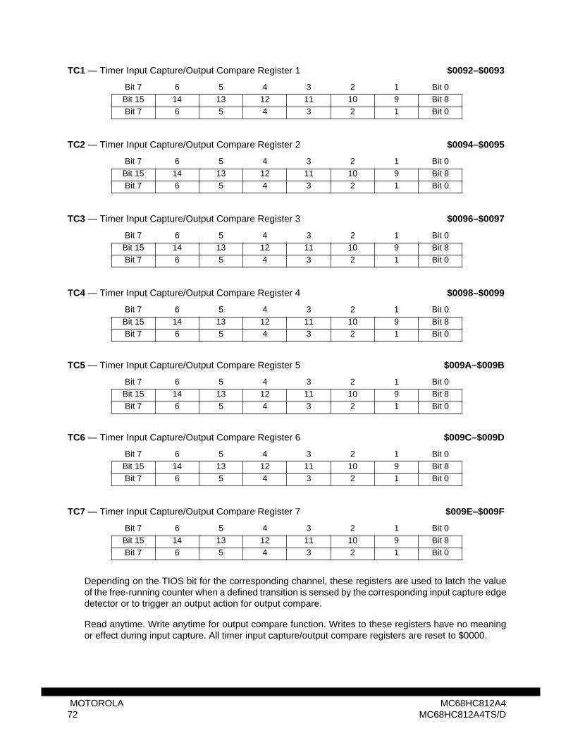
Depending on the TIOS bit for the corresponding channel, these registers are used to latch the valueof the free-running counter when a defined transition is sensed by the corresponding input capture edgedetector or to trigger an output action for output compare.
Read anytime. Write anytime for output compare function. Writes to these registers have no meaningor effect during input capture. All timer input capture/output compare registers are reset to $0000.
TC1 — Timer Input Capture/Output Compare Register 1 $0092–$0093
Bit 7 6 5 4 3 2 1 Bit 0Bit 15 14 13 12 11 10 9 Bit 8Bit 7 6 5 4 3 2 1 Bit 0
TC2 — Timer Input Capture/Output Compare Register 2 $0094–$0095
Bit 7 6 5 4 3 2 1 Bit 0Bit 15 14 13 12 11 10 9 Bit 8Bit 7 6 5 4 3 2 1 Bit 0
TC3 — Timer Input Capture/Output Compare Register 3 $0096–$0097
Bit 7 6 5 4 3 2 1 Bit 0Bit 15 14 13 12 11 10 9 Bit 8Bit 7 6 5 4 3 2 1 Bit 0
TC4 — Timer Input Capture/Output Compare Register 4 $0098–$0099
Bit 7 6 5 4 3 2 1 Bit 0Bit 15 14 13 12 11 10 9 Bit 8Bit 7 6 5 4 3 2 1 Bit 0
TC5 — Timer Input Capture/Output Compare Register 5 $009A–$009B
Bit 7 6 5 4 3 2 1 Bit 0Bit 15 14 13 12 11 10 9 Bit 8Bit 7 6 5 4 3 2 1 Bit 0
TC6 — Timer Input Capture/Output Compare Register 6 $009C–$009D
Bit 7 6 5 4 3 2 1 Bit 0Bit 15 14 13 12 11 10 9 Bit 8Bit 7 6 5 4 3 2 1 Bit 0
TC7 — Timer Input Capture/Output Compare Register 7 $009E–$009F
Bit 7 6 5 4 3 2 1 Bit 0Bit 15 14 13 12 11 10 9 Bit 8Bit 7 6 5 4 3 2 1 Bit 0
MOTOROLA MC68HC812A472 MC68HC812A4TS/D
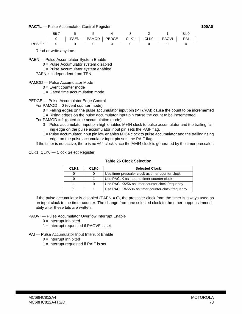
Read or write anytime.
PAEN — Pulse Accumulator System Enable 0 = Pulse Accumulator system disabled1 = Pulse Accumulator system enabled
PAEN is independent from TEN.
PAMOD — Pulse Accumulator Mode 0 = Event counter mode 1 = Gated time accumulation mode
PEDGE — Pulse Accumulator Edge Control For PAMOD = 0 (event counter mode)
0 = Falling edges on the pulse accumulator input pin (PT7/PAI) cause the count to be incremented1 = Rising edges on the pulse accumulator input pin cause the count to be incremented
For PAMOD = 1 (gated time accumulation mode)0 = Pulse accumulator input pin high enables M÷64 clock to pulse accumulator and the trailing fall-
ing edge on the pulse accumulator input pin sets the PAIF flag. 1 = Pulse accumulator input pin low enables M÷64 clock to pulse accumulator and the trailing rising
edge on the pulse accumulator input pin sets the PAIF flag. If the timer is not active, there is no ÷64 clock since the M÷64 clock is generated by the timer prescaler.
CLK1, CLK0 — Clock Select Register
If the pulse accumulator is disabled (PAEN = 0), the prescaler clock from the timer is always used asan input clock to the timer counter. The change from one selected clock to the other happens immedi-ately after these bits are written.
PAOVI — Pulse Accumulator Overflow Interrupt Enable0 = Interrupt inhibited1 = Interrupt requested if PAOVF is set
PAI — Pulse Accumulator Input Interrupt Enable0 = Interrupt inhibited 1 = Interrupt requested if PAIF is set
PACTL — Pulse Accumulator Control Register $00A0
Bit 7 6 5 4 3 2 1 Bit 00 PAEN PAMOD PEDGE CLK1 CLK0 PAOVI PAI
RESET: 0 0 0 0 0 0 0 0
Table 26 Clock Selection
CLK1 CLK0 Selected Clock0 0 Use timer prescaler clock as timer counter clock0 1 Use PACLK as input to timer counter clock1 0 Use PACLK/256 as timer counter clock frequency1 1 Use PACLK/65536 as timer counter clock frequency
MC68HC812A4 MOTOROLAMC68HC812A4TS/D 73

Read or write anytime.
When TFFCA bit in the TSCR register is set, any access to the PACNT register will clear all the flags inthe PAFLG register.
PAOVF — Pulse Accumulator Overflow FlagSet when the 16-bit pulse accumulator overflows from $FFFF to $0000. This bit is cleared automaticallyby a write to the PAFLG register with bit 1 set.
PAIF — Pulse Accumulator Input Edge FlagSet when the selected edge is detected at the pulse accumulator input pin. In event mode, the eventedge triggers PAIF. In gated time accumulation mode, the trailing edge of the gate signal at the pulseaccumulator input pin triggers PAIF. This bit is cleared automatically by a write to the PAFLG registerwith bit 0 set.
Full count register access should take place in one clock cycle. A separate read/write for high byte andlow byte will give a different result than accessing them as a word.
Read or write anytime.
Read anytime. Write only in special mode (SMODN = 0)
TCBYP — Timer Divider Chain Bypass 0 = Normal operation 1 = The 16-bit free-running timer counter is divided into two 8-bit halves and the prescaler is by-
passed. The clock drives both halves directly.
PCBYP — Pulse Accumulator Divider Chain Bypass 0 = Normal operation 1 = The 16-bit pulse accumulator counter is divided into two 8-bit halves and the prescaler is by-
passed. The clock drives both halves directly.
PAFLG — Pulse Accumulator Flag Register $00A1
Bit 7 6 5 4 3 2 1 Bit 00 0 0 0 0 0 PAOVF PAIF
RESET: 0 0 0 0 0 0 0 0
PACNT — 16-bit Pulse Accumulator Count Register $00A2–$00A3
Bit 7 6 5 4 3 2 1 Bit 0Bit 15 14 13 12 11 10 9 Bit 8Bit 7 6 5 4 3 2 1 Bit 0
RESET: 0 0 0 0 0 0 0 0
TIMTST — Timer Test Register $00AD
Bit 7 6 5 4 3 2 1 Bit 00 0 0 0 0 0 TCBYP PCBYP
RESET: 0 0 0 0 0 0 0 0
MOTOROLA MC68HC812A474 MC68HC812A4TS/D

Read anytime (inputs return pin level; outputs return pin driver input level). Write data stored in an in-ternal latch (drives pins only if configured for output).
NOTEWrites do not change pin state when the pin is configured for timer output. The min-imum pulse width for pulse accumulator input should always be greater than twomodule clocks due to input synchronizer circuitry. The minimum pulse width for theinput capture should always be greater than the width of two module clocks due toinput synchronizer circuitry.
Read or write anytime.
0 = Configures the corresponding I/O pin for input only 1 = Configures the corresponding I/O pin for output
The timer forces the I/O state to be an output for each timer port pin associated with an enabled outputcompare. In these cases the data direction bits will not be changed but have no affect on the directionof these pins. The DDRT will revert to controlling the I/O direction of a pin when the associated timeroutput compare is disabled. Input captures do not override the DDRT settings.
13.2 Timer Operation in ModesSTOP: Timer is off since both PCLK and ECLK are stopped. BDM: Timer keeps running, unless TSBCK = 1WAIT: Counters keep running, unless TSWAI = 1NORMAL: Timer keeps running, unless TEN = 0TEN = 0: All timer operations are stopped, registers may be accessed.
Gated pulse accumulator ÷64 clock is also disabled.PAEN = 0: All pulse accumulator operations are stopped, registers may be accessed.
PORTT — Timer Port Data Register $00AE
Bit 7 6 5 4 3 2 1 Bit 0PT7 PT6 PT5 PT4 PT3 PT2 PT1 PT0
TIMER I/OC7 I/OC6 I/OC5 I/OC4 I/OC3 I/OC2 I/OC1 I/OC0PA PAI
DDRT — Data Direction Register for Timer Port $00AF
Bit 7 6 5 4 3 2 1 Bit 0Bit 7 6 5 4 3 2 1 Bit 0
RESET: 0 0 0 0 0 0 0 0
MC68HC812A4 MOTOROLAMC68HC812A4TS/D 75

14 Multiple Serial InterfaceThe multiple serial interface (MSI) module consists of three independent serial I/O sub-systems: twoserial communication interfaces (SCI0 and SCI1) and the serial peripheral interface (SPI0). Each serialpin shares function with the general-purpose port pins of port S. The SCI subsystems are NRZ-type sys-tems that are compatible with standard RS-232 systems. These SCI systems have a new single wireoperation mode which allows the unused pin to be available as general-purpose I/O. The SPI sub-system, which is compatible with the M68HC11 SPI, includes new features such as SS output andbidirectional mode.
14.1 Block diagram
Figure 19 Multiple Serial Interface Block Diagram
14.2 Serial Communication Interface (SCI)
Two serial communication interfaces are available on the MC68HC812A4. These are NRZ format (onestart, eight or nine data, and one stop bit) asynchronous communication systems with independent in-ternal baud rate generation circuitry and SCI transmitters and receivers. They can be configured foreight or nine data bits (one of which may be designated as a parity bit, odd or even). If enabled, parityis generated in hardware for transmitted and received data. Receiver parity errors are flagged in hard-ware. The baud rate generator is based on a modulus counter, allowing flexibility in choosing baudrates. There is a receiver wake-up feature, an idle line detect feature, a loop-back mode, and variouserror detection features. Two port pins for each SCI provide the external interface for the transmitteddata (TXD) and the received data (RXD).
PS0
PS1
PS2
PS3
PS4
PS5
PS6
PS7
SCI0
SCI1
SPI0
DD
RS
/IOC
TLR
PO
RT S
I/O
DR
IVE
RS
MSIRxD0
TxD0
RxD1
TxD1
MISO/SISO
MOSI/MOMI
SCK
CS/SS
HC12A4 MSI BLOCK
MOTOROLA MC68HC812A476 MC68HC812A4TS/D

Figure 20 Serial Communications Interface Block Diagram
14.2.1 Data Format
The serial data format requires the following conditions:
• An idle-line in the high state before transmission or reception of a message.• A start bit (logic zero), transmitted or received, that indicates the start of each character.• Data that is transmitted or received least significant bit (LSB) first.• A stop bit (logic one), used to indicate the end of a frame. (A frame consists of a start bit, a char-
acter of eight or nine data bits and a stop bit.)• A BREAK is defined as the transmission or reception of a logic zero for one frame or more.• This SCI supports hardware parity for transmit and receive.
Rx Baud Rate
Tx Baud Rate
MCLK
DIVIDER 10-11 Bit SHIFT REG
MSB
TxD BUFFER/SCxDRL
TxMTR CONTROL
SCxCR2/SCI CTL 2
SCxCR1/SCI CTL 1
SCxSR1/INT STATUS
DATA RECOVERY
10-11 BIT SHIFT REG
RxD BUFFER/SCxDRL
SCxBD/SELECT
LSB
RxD
TxD
PIN
CO
NT
ROL
/ DD
RS
/ P
ORT S
WAKE-UP LOGICSCxCR1/SCI CTL 1
SCxSR1/INT STATUS
SCxCR2/SCI CTL 2
INT REQUEST LOGIC
MSB LSB
INT REQUEST LOGIC
SCI RECEIVER
SCI TRANSMITTERBAUD RATE
CLOCK
TO INTERNAL
LOGIC
DATA BUS
PARITYDETECT
PARITYGENERATOR
HC12A4 SCI BLOCK
MC68HC812A4 MOTOROLAMC68HC812A4TS/D 77

14.2.2 SCI Baud Rate Generation
The basis of the SCI baud rate generator is a 13-bit modulus counter. This counter gives the generatorthe flexibility necessary to achieve a reasonable level of independence from the CPU operating frequen-cy and still be able to produce standard baud rates with a minimal amount of error. The clock source forthe generator comes from the M Clock.
14.2.3 Register Descriptions
Control and data registers for the SCI subsystem are described below. The memory address indicatedfor each register is the default address that is in use after reset. The entire 512-byte register block canbe mapped to any 2-Kbyte boundary within the standard 64-Kbyte address space. Both SCI have iden-tical control registers mapped in two blocks of eight bytes.
SCxBDH and SCxBDL are considered together as a 16-bit baud rate control register.
Read any time. Write SBR[12:0] anytime. Low order byte must be written for change to take effect. WriteSBR[15:13] only in special modes. The value in SBR[12:0] determines the baud rate of the SCI. Thedesired baud rate is determined by the following formula:
which is equivalent to:
BR is the value written to bits SBR[12:0] to establish baud rate.
Table 27 Baud Rate Generation
DesiredSCI Baud Rate
BR Divisor forM = 4.0 MHz
BR Divisor forM = 8.0 MHz
110 2273 4545300 833 1667600 417 833
1200 208 4172400 104 2084800 52 1049600 26 52
14400 17 3519200 13 2638400 — 13
SC0BDH/SC1BDH — SCI Baud Rate Control Register $00C0/$00C8
Bit 7 6 5 4 3 2 1 Bit 0BTST BSPL BRLD SBR12 SBR11 SBR10 SBR9 SBR8 High
RESET: 0 0 0 0 0 0 0 0
SC0BDL/SC1BDL — SCI Baud Rate Control Register $00C1/$00C9
Bit 7 6 5 4 3 2 1 Bit 0SBR7 SBR6 SBR5 SBR4 SBR3 SBR2 SBR1 SBR0 Low
RESET: 0 0 0 0 0 1 0 0
SCI Baud Rate MCLK16 BR×---------------------=
BR MCLK16 SCI Baud Rate×-----------------------------------------------------=
MOTOROLA MC68HC812A478 MC68HC812A4TS/D

NOTEThe baud rate generator is disabled until TE or RE bit in SCxCR2 register is set forthe first time after reset, and/or the baud rate generator is disabled when SBR[12:0]= 0.
BTST — Reserved for test function
BSPL — Reserved for test function
BRLD — Reserved for test function
Read or write anytime.
LOOPS — SCI LOOP Mode/Single Wire Mode Enable 0 = SCI transmit and receive sections operate normally.1 = SCI receive section is disconnected from the RXD pin and the RXD pin is available as general
purpose I/O. The receiver input is determined by the RSRC bit. The transmitter output is con-trolled by the associated DDRS bit. Both the transmitter and the receiver must be enabled touse the LOOP or the single wire mode.
If the DDRS bit associated with the TXD pin is set during the LOOPS = 1, the TXD pin outputs the SCIwaveform. If the DDRS bit associated with the TXD pin is clear during the LOOPS = 1, the TXD pin be-comes high (IDLE line state) for RSRC = 0 and high impedance for RSRC = 1. Refer to Table 28 .
WOMS — Wired-OR Mode for Serial Pins This bit controls the two pins (TXD and RXD) associated with the SCIx section.
0 = Pins operate in a normal mode with both high and low drive capability. To affect the RXD bit,that bit would have to be configured as an output (via DDRS0/2) which is the single wire casewhen using the SCI. WOMS bit still affects general-purpose output on TXD and RXD pins whenSCIx is not using these pins.
1 = Each pin operates in an open drain fashion if that pin is declared as an output.
RSRC — Receiver SourceWhen LOOPS = 1, the RSRC bit determines the internal feedback path for the receiver.
0 = Receiver input is connected to the transmitter internally (not TXD pin)1 = Receiver input is connected to the TXD pin
SC0CR1/SC1CR1 — SCI Control Register 1 $00C2/$00CA
Bit 7 6 5 4 3 2 1 Bit 0LOOPS WOMS RSRC M WAKE ILT PE PT
RESET: 0 0 0 0 0 0 0 0
Table 28 Loop Mode Functions
LOOPS RSRC DDRS1(3) WOMS Function of Port S Bit 1/3
0 x x x Normal Operations1 0 0 0/1 LOOP mode without TXD output (TXD = High Impedance)1 0 1 0 LOOP mode with TXD output (CMOS)1 0 1 1 LOOP mode with TXD output (open-drain)1 1 0 x Single wire mode without TXD output
(the pin is used as receiver input only, TXD = High Impedance)1 1 1 0 Single wire mode with TXD output
(the output is also fed back to receiver input, CMOS)1 1 1 1 Single wire mode for the receiving and transmitting (open-drain)
MC68HC812A4 MOTOROLAMC68HC812A4TS/D 79

M — Mode (select character format) 0 = One start, eight data, one stop bit1 = One start, eight data, ninth data, one stop bit
WAKE — Wakeup by Address Mark/Idle 0 = Wake up by IDLE line recognition 1 = Wake up by address mark (last data bit set)
ILT — Idle Line Type Determines which of two types of idle line detection will be used by the SCI receiver.
0 = Short idle line mode is enabled.1 = Long idle line mode is detected.
In the short mode, the SCI circuitry begins counting ones in the search for the idle line condition imme-diately after the start bit. This means that the stop bit and any bits that were ones before the stop bitcould be counted in that string of ones, resulting in earlier recognition of an idle line.
In the long mode, the SCI circuitry does not begin counting ones in the search for the idle line conditionuntil a stop bit is received. Therefore, the last byte’s stop bit and preceding “1” bits do not affect howquickly an idle line condition can be detected.
PE — Parity Enable 0 = Parity is disabled.1 = Parity is enabled.
PT — Parity Type If parity is enabled, this bit determines even or odd parity for both the receiver and the transmitter.
0 = Even parity is selected. An even number of ones in the data character causes the parity bit tobe zero and an odd number of ones causes the parity bit to be one.
1 = Odd parity is selected. An odd number of ones in the data character causes the parity bit to bezero and an even number of ones causes the parity bit to be one.
Read or write anytime.
TIE — Transmit Interrupt Enable 0 = TDRE interrupts disabled1 = SCI interrupt will be requested whenever the TDRE status flag is set.
TCIE — Transmit Complete Interrupt Enable 0 = TC interrupts disabled1 = SCI interrupt will be requested whenever the TC status flag is set.
RIE — Receiver Interrupt Enable 0 = RDRF and OR interrupts disabled1 = SCI interrupt will be requested whenever the RDRF status flag or the OR status flag is set.
ILIE — Idle Line Interrupt Enable 0 = IDLE interrupts disabled1 = SCI interrupt will be requested whenever the IDLE status flag is set.
SC0CR2/SC1CR2 — SCI Control Register 2 $00C3/$00CB
Bit 7 6 5 4 3 2 1 Bit 0TIE TCIE RIE ILIE TE RE RWU SBK
RESET: 0 0 0 0 0 0 0 0
MOTOROLA MC68HC812A480 MC68HC812A4TS/D

TE — Transmitter Enable 0 = Transmitter disabled1 = SCI transmit logic is enabled and the TXD pin (port S bit 1/bit 3) is dedicated to the transmitter.
The TE bit can be used to queue an idle preamble.
RE — Receiver Enable 0 = Receiver disabled1 = Enables the SCI receive circuitry.
RWU — Receiver Wake-Up Control0 = Normal SCI Receiver1 = Enables the wake-up function and inhibits further receiver interrupts. Normally hardware wakes
the receiver by automatically clearing this bit.
SBK — Send Break0 = Break generator off1 = Generate a break code (at least ten or eleven contiguous zeros).
As long as SBK remains set the transmitter will send zeros. When SBK is changed to zero, the currentframe of all zeros is finished before the TxD line goes to the idle state. If SBK is toggled on and off, thetransmitter will send only ten (or eleven) zeros and then revert to mark idle or sending data.
The bits in these registers are set by various conditions in the SCI hardware and are automaticallycleared by special acknowledge sequences. The receive related flag bits in SCxSR1 (RDRF, IDLE, OR,NF, FE, and PF) are all cleared by a read of the SCxSR1 register followed by a read of the transmit/receive data register low byte. However, only those bits which were set when SCxSR1 was read will becleared by the subsequent read of the transmit/receive data register low byte. The transmit related bitsin SCxSR1 (TDRE and TC) are cleared by a read of the SCxSR1 register followed by a write to thetransmit/receive data register low byte.
Read anytime (used in auto clearing mechanism). Write has no meaning or effect.
TDRE — Transmit Data Register Empty FlagNew data will not be transmitted unless SCxSR1 is read before writing to the transmit data register. Re-set sets this bit.
0 = SCxDR busy1 = Any byte in the transmit data register is transferred to the serial shift register so new data may
now be written to the transmit data register.
TC — Transmit Complete FlagFlag is set when the transmitter is idle (no data, preamble, or break transmission in progress). Clear byreading SCxSR1 with TC set and then writing to SCxDR.
0 = Transmitter busy1 = Transmitter is idle
RDRF — Receive Data Register Full FlagOnce cleared, IDLE is not set again until the RxD line has been active and becomes idle again. RDRFis set if a received character is ready to be read from SCxDR. Clear the RDRF flag by reading SCxSR1with RDRF set and then reading SCxDR.
0 = SCxDR empty1 = SCxDR full
SC0SR1/SC1SR1 — SCI Status Register 1 $00C4/$00CC
Bit 7 6 5 4 3 2 1 Bit 0TDRE TC RDRF IDLE OR NF FE PF
RESET: 1 1 0 0 0 0 0 0
MC68HC812A4 MOTOROLAMC68HC812A4TS/D 81
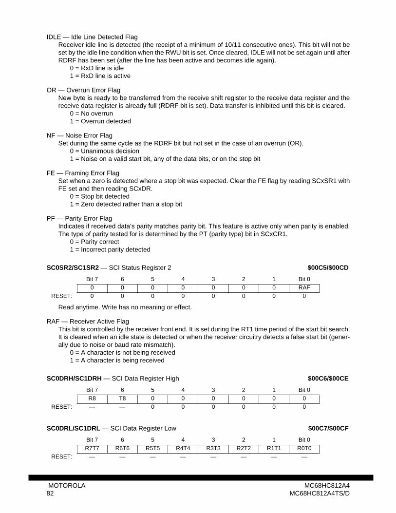
IDLE — Idle Line Detected FlagReceiver idle line is detected (the receipt of a minimum of 10/11 consecutive ones). This bit will not beset by the idle line condition when the RWU bit is set. Once cleared, IDLE will not be set again until afterRDRF has been set (after the line has been active and becomes idle again).
0 = RxD line is idle1 = RxD line is active
OR — Overrun Error FlagNew byte is ready to be transferred from the receive shift register to the receive data register and thereceive data register is already full (RDRF bit is set). Data transfer is inhibited until this bit is cleared.
0 = No overrun1 = Overrun detected
NF — Noise Error FlagSet during the same cycle as the RDRF bit but not set in the case of an overrun (OR).
0 = Unanimous decision1 = Noise on a valid start bit, any of the data bits, or on the stop bit
FE — Framing Error FlagSet when a zero is detected where a stop bit was expected. Clear the FE flag by reading SCxSR1 withFE set and then reading SCxDR.
0 = Stop bit detected1 = Zero detected rather than a stop bit
PF — Parity Error FlagIndicates if received data’s parity matches parity bit. This feature is active only when parity is enabled.The type of parity tested for is determined by the PT (parity type) bit in SCxCR1.
0 = Parity correct1 = Incorrect parity detected
Read anytime. Write has no meaning or effect.
RAF — Receiver Active FlagThis bit is controlled by the receiver front end. It is set during the RT1 time period of the start bit search.It is cleared when an idle state is detected or when the receiver circuitry detects a false start bit (gener-ally due to noise or baud rate mismatch).
0 = A character is not being received1 = A character is being received
SC0SR2/SC1SR2 — SCI Status Register 2 $00C5/$00CD
Bit 7 6 5 4 3 2 1 Bit 00 0 0 0 0 0 0 RAF
RESET: 0 0 0 0 0 0 0 0
SC0DRH/SC1DRH — SCI Data Register High $00C6/$00CE
Bit 7 6 5 4 3 2 1 Bit 0R8 T8 0 0 0 0 0 0
RESET: — — 0 0 0 0 0 0
SC0DRL/SC1DRL — SCI Data Register Low $00C7/$00CF
Bit 7 6 5 4 3 2 1 Bit 0R7T7 R6T6 R5T5 R4T4 R3T3 R2T2 R1T1 R0T0
RESET: — — — — — — — —
MOTOROLA MC68HC812A482 MC68HC812A4TS/D

R8 — Receive Bit 8Read anytime. Write has no meaning or affect.
This bit is the ninth serial data bit received when the SCI system is configured for nine-data-bit opera-tion.
T8 — Transmit Bit 8Read or write anytime.
This bit is the ninth serial data bit transmitted when the SCI system is configured for nine-data-bit oper-ation. When using 9-bit data format this bit does not have to be written for each data word. The samevalue will be transmitted as the ninth bit until this bit is rewritten.
R7T7–R0T0 — Receive/Transmit Data Bits 7 to 0Reads access the eight bits of the read-only SCI receive data register (RDR). Writes access the eightbits of the write-only SCI transmit data register (TDR). SCxDRL:SCxDRH form the 9-bit data word forthe SCI. If the SCI is being used with a 7- or 8-bit data word, only SCxDRL needs to be accessed. If a9-bit format is used, the upper register should be written first to ensure that it is transferred to the trans-mitter shift register with the lower register.
14.3 Serial Peripheral Interface (SPI)
The serial peripheral interface allows the MC68HC812A4 to communicate synchronously with periph-eral devices and other microprocessors. The SPI system in the MC68HC812A4 can operate as a mas-ter or as a slave. The SPI is also capable of interprocessor communications in a multiple master system.
When the SPI is enabled, all pins that are defined by the configuration as inputs will be inputs regardlessof the state of the DDRS bits for those pins. All pins that are defined as SPI outputs will be outputs onlyif the DDRS bits for those pins are set. Any SPI output whose corresponding DDRS bit is cleared canbe used as a general-purpose input.
A bidirectional serial pin is possible using the DDRS as the direction control.
14.3.1 SPI Baud Rate Generation
The E Clock is input to a divider series and the resulting SPI clock rate may be selected to be E dividedby 2, 4, 8, 16, 32, 64, 128 or 256. Three bits in the SP0BR register control the SPI clock rate. This baudrate generator is activated only when SPI is in the master mode and serial transfer is taking place. Oth-erwise this divider is disabled to save power.
14.3.2 SPI Operation
In the SPI system the 8-bit data register in the master and the 8-bit data register in the slave are linkedto form a distributed 16-bit register. When a data transfer operation is performed, this 16-bit register isserially shifted eight bit positions by the SCK clock from the master so the data is effectively exchangedbetween the master and the slave. Data written to the SP0DR register of the master becomes the outputdata for the slave and data read from the SP0DR register of the master after a transfer operation is theinput data from the slave.
MC68HC812A4 MOTOROLAMC68HC812A4TS/D 83

Figure 21 Serial Peripheral Interface Block Diagram
A clock phase control bit (CPHA) and a clock polarity control bit (CPOL) in the SP0CR1 register selectone of four possible clock formats to be used by the SPI system. The CPOL bit simply selects non-in-verted or inverted clock. The CPHA bit is used to accommodate two fundamentally different protocolsby shifting the clock by one half cycle or no phase shift.
PINCONTROL
LOGIC
8-BIT SHIFT REGISTER
READ DATA BUFFER
SHIFT CONTROL LOGIC
CLOCKLOGIC
SPI CONTROL
SP0SR SPI STATUS REGISTER
SP0DR SPI DATA REGISTER
SP
IF
WC
OL
MO
DF
DIVIDER
SELECT
SP0BR SPI BAUD RATE REGISTER
÷2 ÷4 ÷8 ÷16 ÷32 ÷64 ÷128 ÷256
SPIINTERRUPT
INTERNAL BUS
MCU P CLOCK(SAME AS E RATE)
SM
M
S
M
S
SP
R2
SP
R1
SP
R0
REQUEST
SP
IE
SP
E
MS
TR
CP
OL
CP
HA
LSB
F
LSBF
PU
PS
RD
S
SW
OM
SP
C0
SS
OE
SPE
CLOCK
MSTR
SWOM
MISOPS4
SCKPS6
SSPS7
MOSIPS5
HC12 SPI BLOCK
SP0CR1 SPI CONTROL REGISTER 1SP0CR2 SPI CONTROL REGISTE
MOTOROLA MC68HC812A484 MC68HC812A4TS/D

Figure 22 SPI Clock Format 0 (CPHA = 0)
Figure 23 SPI Clock Format 1 (CPHA = 1)
tL
Begin End
SCK (CPOL=0)
SAMPLE I
CHANGE O
SEL SS (O)
Transfer
SCK (CPOL=1)
MSB first (LSBF=0): LSB first (LSBF=1):
MSBLSB
LSBMSB
Bit 5Bit 2
Bit 6Bit 1
Bit 4Bit 3
Bit 3Bit 4
Bit 2Bit 5
Bit 1Bit 6
CHANGE O
SEL SS (I)
(MOSI pin)
(MISO pin)
(Master only)
(MOSI/MISO)
tT
If ne
xt tr
ansf
er b
egin
s he
re
for tT, tl, tLMinimum 1/2 SCK
tI tL
HC12 SPI CLOCK FORM 0
tL tT
for tT, tl, tLMinimum 1/2 SCK
tI tL
If ne
xt tr
ansf
er b
egin
s he
re
Begin End
SCK (CPOL=0)
SAMPLE I
CHANGE O
SEL SS (O)
Transfer
SCK (CPOL=1)
MSB first (LSBF=0): LSB first (LSBF=1):
MSBLSB
LSBMSB
Bit 5Bit 2
Bit 6Bit 1
Bit 4Bit 3
Bit 3Bit 4
Bit 2Bit 5
Bit 1Bit 6
CHANGE O
SEL SS (I)
(MOSI pin)
(MISO pin)
(Master only)
(MOSI/MISO)
HC12 SPI CLOCK FORM 1
MC68HC812A4 MOTOROLAMC68HC812A4TS/D 85

14.3.3 SS Output
Available in master mode only, SS output is enabled with the SSOE bit in the SP0CR1 register if thecorresponding DDRS is set. The SS output pin will be connected to the SS input pin of the external slavedevice. The SS output automatically goes low for each transmission to select the external device and itgoes high during each idling state to deselect external devices.
14.3.4 Bidirectional Mode (MOMI or SISO)
In bidirectional mode, the SPI uses only one serial data pin for external device interface. The MSTR bitdecides which pin to be used. The MOSI pin becomes serial data I/O (MOMI) pin for the master mode,and the MISO pin becomes serial data I/O (SISO) pin for the slave mode. The direction of each serialI/O pin depends on the corresponding DDRS bit.
14.3.5 Register Descriptions
Control and data registers for the SPI subsystem are described below. The memory address indicatedfor each register is the default address that is in use after reset. The entire 512-byte register block canbe mapped to any 2-Kbyte boundary within the standard 64-Kbyte address space. For more informationrefer to 6 Operating Modes and Resource Mapping .
Read or write anytime.
Table 29 SS Output Selection
DDRS7 SSOE Master Mode Slave Mode0 0 SS Input with MODF Feature SS Input0 1 Reserved SS Input1 0 General-Purpose Output SS Input1 1 SS Output SS Input
When SPE=1 Master ModeMSTR=1
Slave ModeMSTR=0
NormalMode
SPC0=0
SWOM enables open drain output. SWOM enables open drain output.
Bidirectional Mode
SPC0=1
SWOM enables open drain output. PS4 becomes GPIO. SWOM enables open drain output. PS5 becomes GPIO.
Figure 24 Normal Mode and Bidirectional Mode
SP0CR1 — SPI Control Register 1 $00D0
Bit 7 6 5 4 3 2 1 Bit 0SPIE SPE SWOM MSTR CPOL CPHA SSOE LSBF
RESET: 0 0 0 0 0 1 0 0
SPI
MO
MI
DDRS5
Serial Out
Serial In
SPI
SI
SO
Serial In
Serial Out
DDRS4
SPI
MOMI
PS4
DDRS5
Serial Out
Serial In
SPI
PS5
SISO
DDRS4
Serial In
Serial Out
MOTOROLA MC68HC812A486 MC68HC812A4TS/D
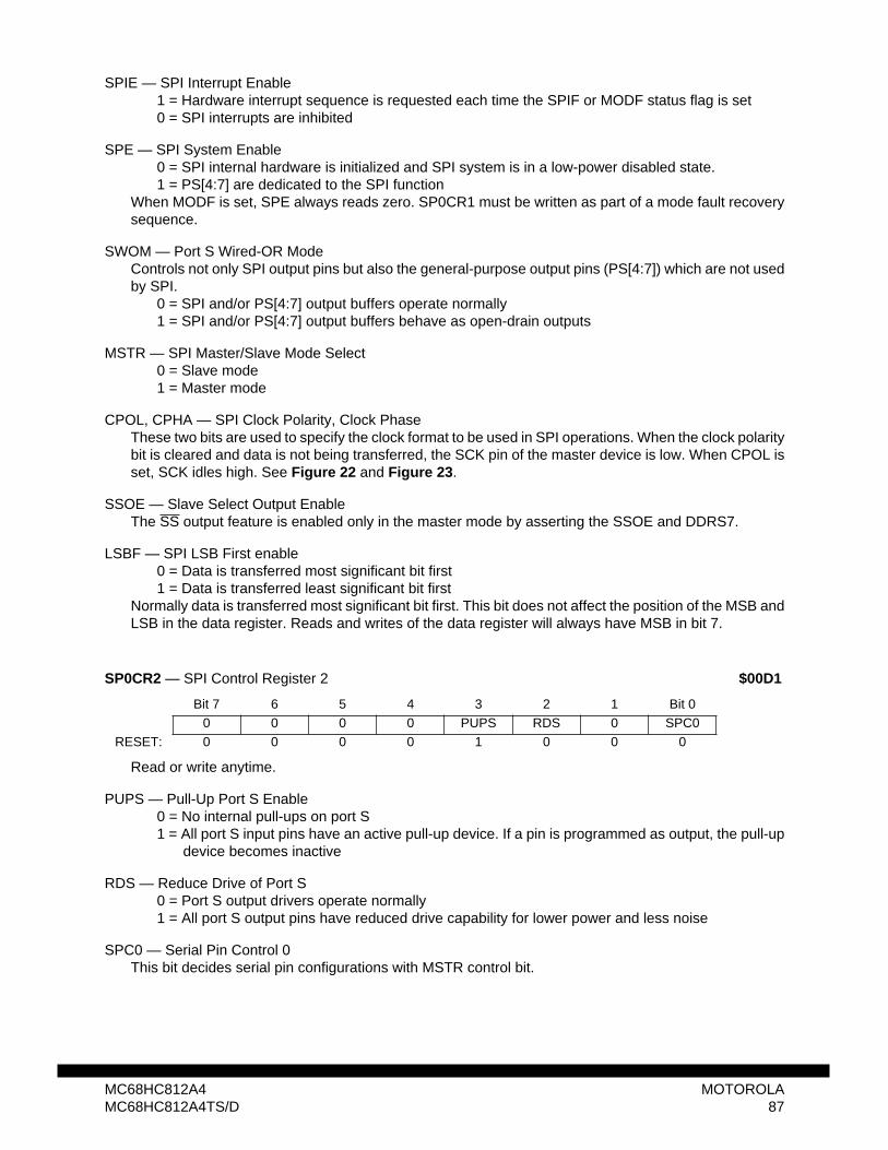
SPIE — SPI Interrupt Enable1 = Hardware interrupt sequence is requested each time the SPIF or MODF status flag is set 0 = SPI interrupts are inhibited
SPE — SPI System Enable0 = SPI internal hardware is initialized and SPI system is in a low-power disabled state.1 = PS[4:7] are dedicated to the SPI function
When MODF is set, SPE always reads zero. SP0CR1 must be written as part of a mode fault recoverysequence.
SWOM — Port S Wired-OR ModeControls not only SPI output pins but also the general-purpose output pins (PS[4:7]) which are not usedby SPI.
0 = SPI and/or PS[4:7] output buffers operate normally1 = SPI and/or PS[4:7] output buffers behave as open-drain outputs
MSTR — SPI Master/Slave Mode Select0 = Slave mode1 = Master mode
CPOL, CPHA — SPI Clock Polarity, Clock PhaseThese two bits are used to specify the clock format to be used in SPI operations. When the clock polaritybit is cleared and data is not being transferred, the SCK pin of the master device is low. When CPOL isset, SCK idles high. See Figure 22 and Figure 23 .
SSOE — Slave Select Output EnableThe SS output feature is enabled only in the master mode by asserting the SSOE and DDRS7.
LSBF — SPI LSB First enable0 = Data is transferred most significant bit first1 = Data is transferred least significant bit first
Normally data is transferred most significant bit first. This bit does not affect the position of the MSB andLSB in the data register. Reads and writes of the data register will always have MSB in bit 7.
Read or write anytime.
PUPS — Pull-Up Port S Enable0 = No internal pull-ups on port S1 = All port S input pins have an active pull-up device. If a pin is programmed as output, the pull-up
device becomes inactive
RDS — Reduce Drive of Port S0 = Port S output drivers operate normally1 = All port S output pins have reduced drive capability for lower power and less noise
SPC0 — Serial Pin Control 0This bit decides serial pin configurations with MSTR control bit.
SP0CR2 — SPI Control Register 2 $00D1
Bit 7 6 5 4 3 2 1 Bit 00 0 0 0 PUPS RDS 0 SPC0
RESET: 0 0 0 0 1 0 0 0
MC68HC812A4 MOTOROLAMC68HC812A4TS/D 87

Read anytime. Write anytime.
At reset, E clock divided by 2 is selected.
SPR[2:0] — SPI Clock (SCK) Rate Select BitsThese bits are used to specify the SPI clock rate.
Read anytime. Write has no meaning or effect.
SPIF — SPI Interrupt RequestSPIF is set after the eighth SCK cycle in a data transfer and it is cleared by reading the SP0SR register(with SPIF set) followed by an access (read or write) to the SPI data register.
1. The serial pin control 0 bit enables bidirectional configurations.2. Slave output is enabled if DDRS4 = 1, SS = 0 and MSTR = 0. (#1, #3)3. Master output is enabled if DDRS5 = 1 and MSTR = 1. (#2, #4)4. SCK output is enabled if DDRS6 = 1 and MSTR = 1. (#2, #4)5. SS output is enabled if DDRS7 = 1, SSOE = 1 and MSTR = 1. (#2, #4)
Pin Mode SPC0 1 MSTR MISO2 MOSI3 SCK4 SS5
#1Normal
0 0 Slave Out Slave In SCK In SS In
#2 1 Master In Master Out SCK Out SS I/O
#3Bidirectional
1 0 Slave I/O GPI/O SCK In SS In
#4 1 GPI/O Master I/O SCK Out SS I/O
SP0BR — SPI Baud Rate Register $00D2
Bit 7 6 5 4 3 2 1 Bit 00 0 0 0 0 SPR2 SPR1 SPR0
RESET: 0 0 0 0 0 0 0 0
Table 30 SPI Clock Rate Selection
SPR2 SPR1 SPR0 E ClockDivisor
Frequency at E Clock = 4 MHz
Frequency at E Clock = 8 MHz
0 0 0 2 2.0 MHz 4.0 MHz0 0 1 4 1.0 MHz 2.0 MHz0 1 0 8 500 kHz 1.0 MHz0 1 1 16 250 kHz 500 kHz1 0 0 32 125 kHz 250 kHz1 0 1 64 62.5 kHz 125 kHz1 1 0 128 31.3 kHz 62.5 kHz1 1 1 256 15.6 kHz 31.3 kHz
SP0SR — SPI Status Register $00D3
Bit 7 6 5 4 3 2 1 Bit 0SPIF WCOL 0 MODF 0 0 0 0
RESET: 0 0 0 0 0 0 0 0
MOTOROLA MC68HC812A488 MC68HC812A4TS/D

WCOL — Write Collision Status FlagThe MCU write is disabled to avoid writing over the data being transferred. No interrupt is generatedbecause the error status flag can be read upon completion of the transfer that was in progress at thetime of the error. Automatically cleared by a read of the SP0SR (with WCOL set) followed by an access(read or write) to the SP0DR register.
0 = No write collision1 = Indicates that a serial transfer was in progress when the MCU tried to write new data into the
SP0DR data register.
MODF — SPI Mode Error Interrupt Status FlagThis bit is set automatically by SPI hardware if the MSTR control bit is set and the slave select input pinbecomes zero. This condition is not permitted in normal operation. In the case where DDRS bit 7 is set,the PS7 pin is a general-purpose output pin or SS output pin rather than being dedicated as the SS inputfor the SPI system. In this special case the mode fault function is inhibited and MODF remains cleared.This flag is automatically cleared by a read of the SP0SR (with MODF set) followed by a write to theSP0CR1 register.
Read anytime (normally only after SPIF flag set). Write anytime (see WCOL write collision flag).
Reset does not affect this address.
This 8-bit register is both the input and output register for SPI data. Reads of this register are doublebuffered but writes cause data to written directly into the serial shifter. In the SPI system the 8-bit dataregister in the master and the 8-bit data register in the slave are linked by the MOSI and MISO wires toform a distributed 16-bit register. When a data transfer operation is performed, this 16-bit register is se-rially shifted eight bit positions by the SCK clock from the master so the data is effectively exchangedbetween the master and the slave. Note that some slave devices are very simple and either accept datafrom the master without returning data to the master or pass data to the master without requiring datafrom the master.
14.4 Port S
In all modes, port S bits PS[7:0] can be used for either general-purpose I/O, or with the SCI and SPIsubsystems. During reset, port S pins are configured as high-impedance inputs (DDRS is cleared).
Read anytime (inputs return pin level; outputs return pin driver input level). Write data stored in internallatch (drives pins only if configured for output). Writes do not change pin state when pin configured forSPI or SCI output.
After reset all bits are configured as general-purpose inputs.
Port S shares function with the on-chip serial systems (SPI0 and SCI0/1).
SP0DR — SPI Data Register $00D5
Bit 7 6 5 4 3 2 1 Bit 0Bit 7 6 5 4 3 2 1 Bit 0
RESET: 0 0 0 0 0 0 0 0
PORTS — Port S Data Register $00D6
Bit 7 6 5 4 3 2 1 Bit 0
PS7 PS6 PS5 PS4 PS3 PS2 PS1 PS0
PinFunction
SSCS
SCK MOSIMOMI
MISOSISO
TXD1 RXD1 TXD0 RXD0
MC68HC812A4 MOTOROLAMC68HC812A4TS/D 89

Read or write anytime.
After reset, all general-purpose I/O are configured for input only.0 = Configure the corresponding I/O pin for input only1 = Configure the corresponding I/O pin for output
DDRS2, DDRS0 — Data Direction for Port S Bit 2 and Bit 0If the SCI receiver is configured for two-wire SCI operation, corresponding port S pins will be input re-gardless of the state of these bits.
DDRS3, DDRS1 — Data Direction for Port S Bit 3 and Bit 1If the SCI transmitter is configured for two-wire SCI operation, corresponding port S pins will be outputregardless of the state of these bits.
DDRS[6:4] — Data Direction for Port S Bits 6 through 4If the SPI is enabled and expects the corresponding port S pin to be an input, it will be an input regard-less of the state of the DDRS bit. If the SPI is enabled and expects the bit to be an output, it will be anoutput ONLY if the DDRS bit is set.
DDRS7 — Data Direction for Port S Bit 7In SPI slave mode, DDRS7 has no meaning or effect; the PS7 pin is dedicated as the SS input. In SPImaster mode, DDRS7 determines whether PS7 is an error detect input to the SPI or a general-purposeor slave select output line.
DDRS — Data Direction Register for Port S $00D7
Bit 7 6 5 4 3 2 1 Bit 0Bit 7 6 5 4 3 2 1 Bit 0
RESET: 0 0 0 0 0 0 0 0
MOTOROLA MC68HC812A490 MC68HC812A4TS/D

15 Analog-to-Digital ConverterThe ATD is an 8-channel, 8-bit, multiplexed-input successive-approximation analog-to-digital converter,accurate to ±1 least significant bit (LSB). It does not require external sample and hold circuits becauseof the type of charge redistribution technique used. The ATD converter timing can be synchronized tothe system P clock. The ATD module consists of a 16-word (32-byte) memory-mapped control registerblock used for control, testing and configuration.
Figure 25 Analog-to-Digital Converter Block Diagram
15.1 Functional Description
A single conversion sequence consists of four or eight conversions, depending on the state of the select8 channel mode (S8CM) bit when ATDCTL5 is written. There are eight basic conversion modes. In thenon-scan modes, the SCF bit is set after the sequence of four or eight conversions has been performedand the ATD module halts. In the scan modes, the SCF bit is set after the first sequence of four or eightconversions has been performed, and the ATD module continues to restart the sequence. In bothmodes, the CCF bit associated with each register is set when that register is loaded with the appropriateconversion result. That flag is cleared automatically when that result register is read. The conversionsare started by writing to the control registers.
MO
DE
AN
D TIM
ING
CO
NT
ROLS
ATD 0
ATD 1
ATD 2
ATD 3
ATD 4
ATD 5
ATD 6
ATD 7
SAR
RC DAC ARRAYAND COMPARATOR
INTERNAL BUS
VDDA
VSSA
VRL
VRH
CLOCKSELECT/PRESCALE
ANALOG MUXAND
SAMPLE BUFFER AMP
PORT ADDATA INPUT REGISTER
AN7/PAD7AN6/PAD6AN5/PAD5AN4/PAD4AN3/PAD3AN2/PAD2AN1/PAD1AN0/PAD0
REFERENCE
SUPPLY
HC12 ATD BLOCK
MC68HC812A4 MOTOROLAMC68HC812A4TS/D 91
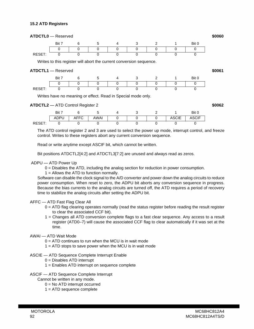
15.2 ATD Registers
Writes to this register will abort the current conversion sequence.
Writes have no meaning or effect. Read in Special mode only.
The ATD control register 2 and 3 are used to select the power up mode, interrupt control, and freezecontrol. Writes to these registers abort any current conversion sequence.
Read or write anytime except ASCIF bit, which cannot be written.
Bit positions ATDCTL2[4:2] and ATDCTL3[7:2] are unused and always read as zeros.
ADPU — ATD Power Up0 = Disables the ATD, including the analog section for reduction in power consumption.1 = Allows the ATD to function normally.
Software can disable the clock signal to the A/D converter and power down the analog circuits to reducepower consumption. When reset to zero, the ADPU bit aborts any conversion sequence in progress.Because the bias currents to the analog circuits are turned off, the ATD requires a period of recoverytime to stabilize the analog circuits after setting the ADPU bit.
AFFC — ATD Fast Flag Clear All 0 = ATD flag clearing operates normally (read the status register before reading the result register
to clear the associated CCF bit).1 = Changes all ATD conversion complete flags to a fast clear sequence. Any access to a result
register (ATD0–7) will cause the associated CCF flag to clear automatically if it was set at thetime.
AWAI — ATD Wait Mode0 = ATD continues to run when the MCU is in wait mode1 = ATD stops to save power when the MCU is in wait mode
ASCIE — ATD Sequence Complete Interrupt Enable 0 = Disables ATD interrupt1 = Enables ATD interrupt on sequence complete
ASCIF — ATD Sequence Complete Interrupt Cannot be written in any mode.
0 = No ATD interrupt occurred1 = ATD sequence complete
ATDCTL0 — Reserved $0060
Bit 7 6 5 4 3 2 1 Bit 00 0 0 0 0 0 0 0
RESET: 0 0 0 0 0 0 0 0
ATDCTL1 — Reserved $0061
Bit 7 6 5 4 3 2 1 Bit 00 0 0 0 0 0 0 0
RESET: 0 0 0 0 0 0 0 0
ATDCTL2 — ATD Control Register 2 $0062
Bit 7 6 5 4 3 2 1 Bit 0ADPU AFFC AWAI 0 0 0 ASCIE ASCIF
RESET: 0 0 0 0 0 0 0 0
MOTOROLA MC68HC812A492 MC68HC812A4TS/D

FRZ1, FRZ0 — Background Debug (Freeze) Enable (suspend module operation at breakpoint)When debugging an application, it is useful in many cases to have the ATD pause when a breakpointis encountered. These two bits determine how the ATD will respond when background debug mode be-comes active.
The ATD control register 4 is used to select the clock source and set up the prescaler. Writes to the ATDcontrol registers initiate a new conversion sequence. If a write occurs while a conversion is in progress,the conversion is aborted and ATD activity halts until a write to ATDCTL5 occurs.
SMP1, SMP0 — Select Sample TimeThese bits are used to select one of four sample times after the buffered sample and transfer has oc-curred. Total conversion time depends on initial sample time (two ATD clocks), transfer time (four ATDclocks), final sample time (programmable, refer to Table 32 ), and resolution time (ten ATD clocks).
PRS4, PRS3, PRS2, PRS1, PRS0 — Select Divide-By Factor for ATD P-Clock Prescaler.The binary value written to these bits selects the divide-by factor for the modulo counter-based prescal-er. The P clock is divided by this value plus one and then fed into a ÷2 circuit to generate the ATD mod-ule clock. The divide-by-two circuit insures symmetry of the output clock signal. Clearing these bitscauses the prescale value default to one which results in a ÷2 prescale factor. This signal is then fedinto the ÷2 logic. The reset state divides the P clock by a total of four and is appropriate for nominaloperation at 2 MHz. Table 33 shows the divide-by operation and the appropriate range of system clockfrequencies.
ATDCTL3 — ATD Control Register 3 $0063
Bit 7 6 5 4 3 2 1 Bit 00 0 0 0 0 0 FRZ1 FRZ0
RESET: 0 0 0 0 0 0 0 0
Table 31 ATD Response to Background Debug Enable
FRZ1 FRZ0 ATD Response0 0 Continue conversions in active background mode0 1 Reserved1 0 Finish current conversion, then freeze1 1 Freeze when BDM is active
ATDCTL4 — ATD Control Register 4 $0064
Bit 7 6 5 4 3 2 1 Bit 00 SMP1 SMP0 PRS4 PRS3 PRS2 PRS1 PRS0
RESET: 0 0 0 0 0 0 0 1
Table 32 Final Sample Time Selection
SMP1 SMP0 Final Sample Time Total 8-Bit Conversion Time
0 0 2 ATD clock periods 18 ATD clock periods
0 1 4 ATD clock periods 20 ATD clock periods
1 0 8 ATD clock periods 24 ATD clock periods
1 1 16 ATD clock periods 32 ATD clock periods
MC68HC812A4 MOTOROLAMC68HC812A4TS/D 93

The ATD control register 5 is used to select the conversion modes, the conversion channel(s), and ini-tiate conversions.
Read or write any time. A write to ATDCTL5 initiates a new conversion sequence. If a conversion se-quence is in progress when a write occurs, that sequence is aborted and the SCF and CCF bits arereset.
S8CM — Select 8 Channel Mode0 = Conversion sequence consists of four conversions1 = Conversion sequence consists of eight conversions
SCAN — Enable Continuous Channel Scan0 = Single conversion sequence1 = Continuous conversion sequences (scan mode)
When a conversion sequence is initiated by a write to the ATDCTL register, the user has a choice ofperforming a sequence of four (or eight, depending on the S8CM bit) conversions or continuously per-forming four (or eight) conversion sequences.
MULT — Enable Multichannel Conversion0 = ATD sequencer runs all four or eight conversions on a single input channel selected via the
CD, CC, CB, and CA bits.1 = ATD sequencer runs each of the four or eight conversions on sequential channels in a specific
group. Refer to Table 34 .
1. Maximum conversion frequency is 2 MHz. Maximum P clock divisor value will becomemaximum conversion rate that can be used on this ATD module.
2. Minimum conversion frequency is 500 kHz. Minimum P clock divisor value will becomeminimum conversion rate that this ATD can perform.
Table 33 Clock Prescaler Values
Prescale Value Total Divisor Max P Clock 1 Min P Clock 2
00000 ÷2 4 MHz 1 MHz
00001 ÷4 8 MHz 2 MHz
00010 ÷6 8 MHz 3 MHz
00011 ÷8 8 MHz 4 MHz
00100 ÷10 8 MHz 5 MHz
00101 ÷12 8 MHz 6 MHz
00110 ÷14 8 MHz 7 MHz
00111 ÷16 8 MHz 8 MHz
01xxx Do Not Use1xxxx
ATDCTL5 — ATD Control Register 5 $0065
Bit 7 6 5 4 3 2 1 Bit 00 S8CM SCAN MULT CD CC CB CA
RESET: 0 0 0 0 0 0 0 0
MOTOROLA MC68HC812A494 MC68HC812A4TS/D

CD, CC, CB, and CA — Channel Select for Conversion
Table 34 Multichannel Mode Result Register Assignment
S8CM CD CC CB CA Channel SignalResult in ADRx
if MULT = 10 0 0 0 0 AN0 ADR0
0 1 AN1 ADR11 0 AN2 ADR21 1 AN3 ADR3
0 0 1 0 0 AN4 ADR00 1 AN5 ADR11 0 AN6 ADR21 1 AN7 ADR3
0 1 0 0 0 Reserved ADR00 1 Reserved ADR11 0 Reserved ADR21 1 Reserved ADR3
0 1 1 0 0 VRH ADR0
0 1 VRL ADR1
1 0 (VRH + VRL)/2 ADR2
1 1 TEST/Reserved ADR31 0 0 0 0 AN0 ADR0
0 0 1 AN1 ADR10 1 0 AN2 ADR20 1 1 AN3 ADR31 0 0 AN4 ADR41 0 1 AN5 ADR51 1 0 AN6 ADR61 1 1 AN7 ADR7
1 1 0 0 0 Reserved ADR00 0 1 Reserved ADR10 1 0 Reserved ADR20 1 1 Reserved ADR31 0 0 VRH ADR4
1 0 1 VRL ADR5
1 1 0 (VRH + VRL)/2 ADR6
1 1 1 TEST/Reserved ADR7Shaded bits are “don’t care” if MULT = 1 and the entire block of four or eight channels make up a conversion sequence. When MULT = 0, all four bits (CD, CC, CB, and CA) must be specified and a conversion sequence con-sists of four or eight consecutive conversions of the single specified chan-nel.
MC68HC812A4 MOTOROLAMC68HC812A4TS/D 95
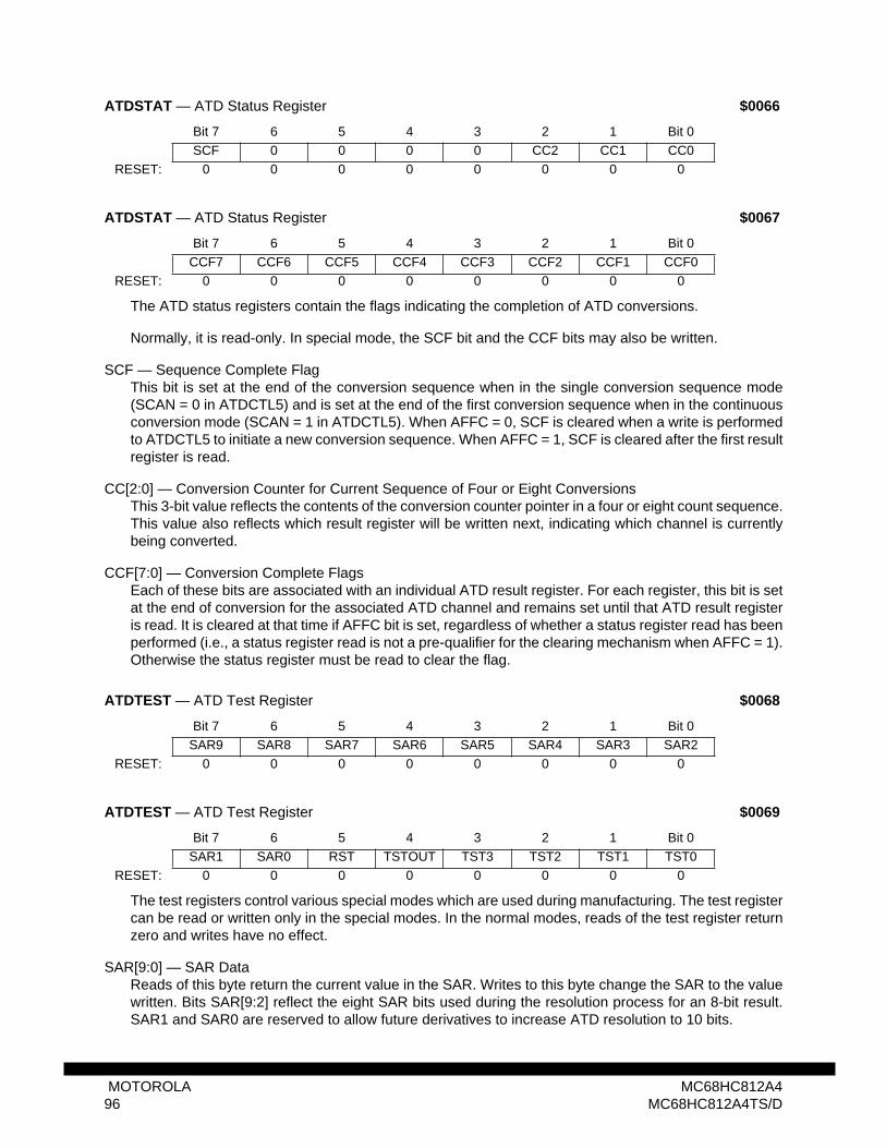
The ATD status registers contain the flags indicating the completion of ATD conversions.
Normally, it is read-only. In special mode, the SCF bit and the CCF bits may also be written.
SCF — Sequence Complete FlagThis bit is set at the end of the conversion sequence when in the single conversion sequence mode(SCAN = 0 in ATDCTL5) and is set at the end of the first conversion sequence when in the continuousconversion mode (SCAN = 1 in ATDCTL5). When AFFC = 0, SCF is cleared when a write is performedto ATDCTL5 to initiate a new conversion sequence. When AFFC = 1, SCF is cleared after the first resultregister is read.
CC[2:0] — Conversion Counter for Current Sequence of Four or Eight ConversionsThis 3-bit value reflects the contents of the conversion counter pointer in a four or eight count sequence.This value also reflects which result register will be written next, indicating which channel is currentlybeing converted.
CCF[7:0] — Conversion Complete FlagsEach of these bits are associated with an individual ATD result register. For each register, this bit is setat the end of conversion for the associated ATD channel and remains set until that ATD result registeris read. It is cleared at that time if AFFC bit is set, regardless of whether a status register read has beenperformed (i.e., a status register read is not a pre-qualifier for the clearing mechanism when AFFC = 1).Otherwise the status register must be read to clear the flag.
The test registers control various special modes which are used during manufacturing. The test registercan be read or written only in the special modes. In the normal modes, reads of the test register returnzero and writes have no effect.
SAR[9:0] — SAR DataReads of this byte return the current value in the SAR. Writes to this byte change the SAR to the valuewritten. Bits SAR[9:2] reflect the eight SAR bits used during the resolution process for an 8-bit result.SAR1 and SAR0 are reserved to allow future derivatives to increase ATD resolution to 10 bits.
ATDSTAT — ATD Status Register $0066
Bit 7 6 5 4 3 2 1 Bit 0SCF 0 0 0 0 CC2 CC1 CC0
RESET: 0 0 0 0 0 0 0 0
ATDSTAT — ATD Status Register $0067
Bit 7 6 5 4 3 2 1 Bit 0CCF7 CCF6 CCF5 CCF4 CCF3 CCF2 CCF1 CCF0
RESET: 0 0 0 0 0 0 0 0
ATDTEST — ATD Test Register $0068
Bit 7 6 5 4 3 2 1 Bit 0SAR9 SAR8 SAR7 SAR6 SAR5 SAR4 SAR3 SAR2
RESET: 0 0 0 0 0 0 0 0
ATDTEST — ATD Test Register $0069
Bit 7 6 5 4 3 2 1 Bit 0SAR1 SAR0 RST TSTOUT TST3 TST2 TST1 TST0
RESET: 0 0 0 0 0 0 0 0
MOTOROLA MC68HC812A496 MC68HC812A4TS/D
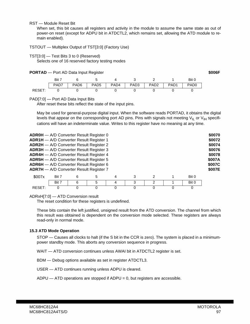
RST — Module Reset BitWhen set, this bit causes all registers and activity in the module to assume the same state as out ofpower-on reset (except for ADPU bit in ATDCTL2, which remains set, allowing the ATD module to re-main enabled).
TSTOUT — Multiplex Output of TST[3:0] (Factory Use)
TST[3:0] — Test Bits 3 to 0 (Reserved)Selects one of 16 reserved factory testing modes
PAD[7:0] — Port AD Data Input BitsAfter reset these bits reflect the state of the input pins.
May be used for general-purpose digital input. When the software reads PORTAD, it obtains the digitallevels that appear on the corresponding port AD pins. Pins with signals not meeting VIL or VIH specifi-cations will have an indeterminate value. Writes to this register have no meaning at any time.
ADRxH[7:0] — ATD Conversion resultThe reset condition for these registers is undefined.
These bits contain the left justified, unsigned result from the ATD conversion. The channel from whichthis result was obtained is dependent on the conversion mode selected. These registers are alwaysread-only in normal mode.
15.3 ATD Mode Operation
STOP — Causes all clocks to halt (if the S bit in the CCR is zero). The system is placed in a minimum-power standby mode. This aborts any conversion sequence in progress.
WAIT — ATD conversion continues unless AWAI bit in ATDCTL2 register is set.
BDM — Debug options available as set in register ATDCTL3.
USER — ATD continues running unless ADPU is cleared.
ADPU — ATD operations are stopped if ADPU = 0, but registers are accessible.
PORTAD — Port AD Data Input Register $006F
Bit 7 6 5 4 3 2 1 Bit 0PAD7 PAD6 PAD5 PAD4 PAD3 PAD2 PAD1 PAD0
RESET: 0 0 0 0 0 0 0 0
ADR0H — A/D Converter Result Register 0 $0070ADR1H — A/D Converter Result Register 1 $0072ADR2H — A/D Converter Result Register 2 $0074ADR3H — A/D Converter Result Register 3 $0076ADR4H — A/D Converter Result Register 4 $0078ADR5H — A/D Converter Result Register 5 $007AADR6H — A/D Converter Result Register 6 $007CADR7H — A/D Converter Result Register 7 $007E
$007x Bit 7 6 5 4 3 2 1 Bit 0
Bit 7 6 5 4 3 2 1 Bit 0RESET: 0 0 0 0 0 0 0 0
MC68HC812A4 MOTOROLAMC68HC812A4TS/D 97

16 Development SupportDevelopment support involves complex interactions between MC68HC812A4 resources and externaldevelopment systems. The following section concerns instruction queue and queue tracking signals,background debug mode, and instruction tagging.
16.1 Instruction Queue
The CPU12 instruction queue provides at least three bytes of program information to the CPU wheninstruction execution begins. The CPU12 always completely finishes executing an instruction before be-ginning to execute the next instruction. Status signals IPIPE[1:0] provide information about data move-ment in the queue and indicate when the CPU begins to execute instructions. This makes it possible tomonitor CPU activity on a cycle-by-cycle basis for debugging. Information available on the IPIPE[1:0]pins is time multiplexed. External circuitry can latch data movement information on rising edges of theE-clock signal; execution start information can be latched on falling edges. Table 35 shows the meaningof data on the pins.
Program information is fetched a few cycles before it is used by the CPU. In order to monitor cycle-by-cycle CPU activity, it is necessary to externally reconstruct what is happening in the instruction queue.Internally the MCU only needs to buffer the data from program fetches. For system debug it is necessaryto keep the data and its associated address in the reconstructed instruction queue. The raw signals re-quired for reconstruction of the queue are ADDR, DATA, R/W, ECLK, and status signals IPIPE[1:0].
The instruction queue consists of two 16-bit queue stages and a holding latch on the input of the firststage. To advance the queue means to move the word in the first stage to the second stage and movethe word from either the holding latch or the data bus input buffer into the first stage. To start even (orodd) instruction means to execute the opcode in the high-order (or low-order) byte of the second stageof the instruction queue.
16.2 Background Debug Mode
Background debug mode (BDM) is used for system development, in-circuit testing, field testing, andprogramming. BDM is implemented in on-chip hardware and provides a full set of debug options.
Because BDM control logic does not reside in the CPU, BDM hardware commands can be executedwhile the CPU is operating normally. The control logic generally uses CPU dead cycles to execute these
1. Refers to data that was on the bus at the previous E falling edge.2. Refers to bus cycle starting at this E falling edge.
Table 35 IPIPE Decoding
Data Movement — IPIPE[1:0] Captured at Rising Edge of E Clock 1
IPIPE[1:0] Mnemonic Meaning
0:0 — No Movement
0:1 LAT Latch Data From Bus
1:0 ALD Advance Queue and Load From Bus
1:1 ALL Advance Queue and Load From Latch
Execution Start — IPIPE[1:0] Captured at Falling Edge of E Clock 2
IPIPE[1:0] Mnemonic Meaning
0:0 — No Start
0:1 INT Start Interrupt Sequence
1:0 SEV Start Even Instruction
1:1 SOD Start Odd Instruction
MOTOROLA MC68HC812A498 MC68HC812A4TS/D

commands, but can steal cycles from the CPU when necessary. Other BDM commands are firmwarebased, and require the CPU to be in active background mode for execution. While BDM is active, theCPU executes a firmware program located in a small on-chip ROM that is available in the standard 64-Kbyte memory map only while BDM is active.
The BDM control logic communicates with an external host development system serially, via the BKGDpin. This single-wire approach minimizes the number of pins needed for development support.
16.2.1 BDM Serial Interface
The BDM serial interface requires the external controller to generate a falling edge on the BKGD pin toindicate the start of each bit time. The external controller provides this falling edge whether data is trans-mitted or received.
BKGD is a pseudo-open-drain pin that can be driven either by an external controller or by the MCU.Data is transferred MSB first at 16 E-clock cycles per bit (nominal speed). The interface times out if 512E-clock cycles occur between falling edges from the host. The hardware clears the command registerwhen this time-out occurs.
The BKGD pin can receive a high or low level or transmit a high or low level. The following diagramsshow timing for each of these cases. Interface timing is synchronous to MCU clocks but asynchronousto the external host. The internal clock signal is shown for reference in counting cycles.
Figure 26 shows an external host transmitting a logic one or zero to the BKGD pin of a target M68HC12MCU. The host is asynchronous to the target so there is a 0-to-1 cycle delay from the host-generatedfalling edge to where the target perceives the beginning of the bit time. Ten target E cycles later, thetarget senses the bit level on the BKGD pin. Typically the host actively drives the pseudo-open-drainBKGD pin during host-to-target transmissions to speed up rising edges. Since the target does not drivethe BKGD pin during this period, there is no need to treat the line as an open-drain signal during host-to-target transmissions.
Figure 26 BDM Host to Target Serial Bit Timing
HC12A4 BDM HOST TO TARGET T
EARLIESTSTART OFNEXT BIT
TARGET SENSES BIT
10 CYCLES
SYNCHRONIZATIONUNCERTAINTY
E CLOCK(TARGET MCU)
HOSTTRANSMIT 1
HOSTTRANSMIT 0
PERCEIVED START
OF BIT TIME
MC68HC812A4 MOTOROLAMC68HC812A4TS/D 99

Figure 27 BDM Target to Host Serial Bit Timing (Logic 1)
Figure 27 shows the host receiving a logic one from the target MC68HC812A4 MCU. Since the host isasynchronous to the target MCU, there is a 0-to-1 cycle delay from the host-generated falling edge onBKGD to the perceived start of the bit time in the target MCU. The host holds the BKGD pin low longenough for the target to recognize it (at least two target E cycles). The host must release the low drivebefore the target MCU drives a brief active-high speed-up pulse seven cycles after the perceived startof the bit time. The host should sample the bit level about ten cycles after it started the bit time.
Figure 28 BDM Target to Host Serial Bit Timing (Logic 0)
Figure 28 shows the host receiving a logic zero from the target MC68HC812A4 MCU. Since the hostis asynchronous to the target MCU, there is a 0-to-1 cycle delay from the host-generated falling edge
HC12A4 BDM TARGET TO HOST
HIGH-IMPEDANCE
HIGH-IMPEDANCE
HIGH-IMPEDANCE
EARLIESTSTART OFNEXT BIT
R-C RISE
10 CYCLES
10 CYCLES
HOST SAMPLESBKGD PIN
PERCEIVEDSTART OF BIT
TIME
BKGD PIN
E CLOCK(TARGET
MCU)
HOSTDRIVE TOBKGD PIN
TARGET MCUSPEEDUP
PULSE
10 CYCLES
E CLOCK(TARGET
MCU)
BKGD PIN
PERCEIVEDSTART OF BIT TIME
10 CYCLES
HOST SAMPLESBKGD PIN
HOSTDRIVE TOBKGD PIN
TARGET MCUDRIVE AND
SPEEDUP PULSE
HIGH-IMPEDANCE
SPEEDUP PULSE
HC12A4 BDM TARGET TO HOST T
EARLIESTSTART OFNEXT BIT
MOTOROLA MC68HC812A4100 MC68HC812A4TS/D

on BKGD to the start of the bit time as perceived by the target MCU. The host initiates the bit time butthe target MC68HC812A4 finishes it. Since the target wants the host to receive a logic zero, it drivesthe BKGD pin low for 13 E-clock cycles, then briefly drives it high to speed up the rising edge. The hostsamples the bit level about ten cycles after starting the bit time.
16.2.2 Enabling BDM Firmware Commands
BDM is available in all operating modes, but must be made active before firmware commands can beexecuted. BDM is enabled by setting the ENBDM bit in the BDM STATUS register via the single wireinterface (using a hardware command; WRITE_BD_BYTE at $FF01). BDM must then be activated tomap BDM registers and ROM to addresses $FF00 to $FFFF and to put the MCU in active backgroundmode.
After the firmware is enabled, BDM can be activated by the hardware BACKGROUND command, bythe BDM tagging mechanism, or by the CPU BGND instruction. An attempt to activate BDM before firm-ware has been enabled causes the MCU to resume normal instruction execution after a brief delay.
BDM becomes active at the next instruction boundary following execution of the BDM BACKGROUNDcommand, but tags activate BDM before a tagged instruction is executed.
In special single-chip mode, background operation is enabled and active immediately out of reset. Thisactive case replaces the M68HC11 boot function, and allows programming a system with blank mem-ory.
While BDM is active, a set of BDM control registers are mapped to addresses $FF00 to $FF06. TheBDM control logic uses these registers which can be read anytime by BDM logic, not user programs.Refer to 16.2.4 BDM Registers for detailed descriptions.
Some on-chip peripherals have a BDM control bit which allows suspending the peripheral function dur-ing BDM. For example, if the timer control is enabled, the timer counter is stopped while in BDM. Oncenormal program flow is continued, the timer counter is re-enabled to simulate real-time operations.
16.2.3 BDM Commands
All BDM command opcodes are eight bits long, and can be followed by an address and/or data, as in-dicated by the instruction. These commands do not require the CPU to be in active BDM mode for ex-ecution.
The host controller must wait 150 cycles for a non-intrusive BDM command to execute before anothercommand can be sent. This delay includes 128 cycles for the maximum delay for a dead cycle. For dataread commands, the host must insert this delay between sending the address and attempting to readthe data.
BDM logic retains control of the internal buses until a read or write is completed. If an operation can becompleted in a single cycle, it does not intrude on normal CPU operation. However, if an operation re-quires multiple cycles, CPU clocks are frozen until the operation is complete.
MC68HC812A4 MOTOROLAMC68HC812A4TS/D 101

The CPU must be in background mode to execute commands that are implemented in the BDM ROM.The BDM ROM is located at $FF20 to $FFFF while BDM is active. There are also seven bytes of BDMregisters which are located at $FF00 to $FF06 while BDM is active. The CPU executes code from thisROM to perform the requested operation. These commands are shown in Table 37 .
1. STATUS command is a specific case of the READ_BD_BYTE command.2. ENABLE_FIRMWARE is a specific case of the WRITE_BD_BYTE command.
Table 36 BDM Commands Implemented in Hardware
Command Opcode (Hex) Data Description
BACKGROUND 90 None Enter background mode (if firmware enabled).
READ_BD_BYTE E416-bit address16-bit data out
Read from memory with BDM in map (may steal cycles if external access) data for odd address on low byte, data for even address on high byte.
STATUS1 E4
FF01, 0000 0000 (out)
READ_BD_BYTE $FF01. Running user code (BGND instruction is not allowed).
FF01,1000 0000 (out)
READ_BD_BYTE $FF01. BGND instruction is allowed.
FF01, 1100 0000 (out)
READ_BD_BYTE $FF01. Background mode active (waiting for single wire serial command).
READ_BD_WORD EC16-bit address 16-bit data out
Read from memory with BDM in map (may steal cycles if external access) must be aligned access.
READ_BYTE E016-bit address16-bit data out
Read from memory with BDM out of map (may steal cy-cles if external access) data for odd address on low byte, data for even address on high byte.
READ_WORD E816-bit address16-bit data out
Read from memory with BDM out of map (may steal cy-cles if external access) must be aligned access.
WRITE_BD_BYTE C416-bit address 16-bit data in
Write to memory with BDM in map (may steal cycles if external access) data for odd address on low byte, data for even address on high byte.
ENABLE_ FIRMWARE2 C4FF01,
1xxx xxxx(in)
Write byte $FF01, set the ENBDM bit. This allows exe-cution of commands which are implemented in firm-ware. Typically, read STATUS, OR in the MSB, write the result back to STATUS.
WRITE_BD_WORD CC16-bit address 16-bit data in
Write to memory with BDM in map (may steal cycles if external access) must be aligned access.
WRITE_BYTE C016-bit address 16-bit data in
Write to memory with BDM out of map (may steal cycles if external access) data for odd address on low byte, data for even address on high byte.
WRITE_WORD C816-bit address 16-bit data in
Write to memory with BDM out of map (may steal cycles if external access) must be aligned access.
MOTOROLA MC68HC812A4102 MC68HC812A4TS/D

16.2.4 BDM Registers
Seven BDM registers are mapped into the standard 64-Kbyte address space when BDM is active. Theregisters can be accessed with the hardware READ_BD and WRITE_BD commands, but must not bewritten during BDM operation. Most users will only be interested in the STATUS register at $FF01; otherregisters are only for use by BDM firmware and logic.
The instruction register is discussed for two conditions: when a hardware command is executed andwhen a firmware command is executed.
The bits in the BDM instruction register have the following meanings when a hardware command isexecuted.
H/F — Hardware/Firmware Flag0 = Firmware instruction1 = Hardware instruction
DATA — Data Flag0 = No data1 = Data included in command
R/W — Read/Write Flag0 = Write1 = Read
Table 37 BDM Firmware Commands
Command Opcode (Hex) Data Description
READ_NEXT 62 16-bit data out X = X + 2; Read next word pointed-to by X
READ_PC 63 16-bit data out Read program counter
READ_D 64 16-bit data out Read D accumulator
READ_X 65 16-bit data out Read X index register
READ_Y 66 16-bit data out Read Y index register
READ_SP 67 16-bit data out Read stack pointer
WRITE_NEXT 42 16-bit data in X = X + 2; Write next word pointed-to by X
WRITE_PC 43 16-bit data in Write program counter
WRITE_D 44 16-bit data in Write D accumulator
WRITE_X 45 16-bit data in Write X index register
WRITE_Y 46 16-bit data in Write Y index register
WRITE_SP 47 16-bit data in Write stack pointer
GO 08 None Go to user program
TRACE1 10 None Execute one user instruction then return to BDM
TAGGO 18 None Enable tagging and go to user program
INSTRUCTION — BDM Instruction Register (hardware command) (BDM) $FF00
Bit 7 6 5 4 3 2 1 Bit 0
H/F DATA R/W BKGND W/B BD/U 0 0
RESET: 0 0 0 0 0 0 0 0
MC68HC812A4 MOTOROLAMC68HC812A4TS/D 103

BKGND — Hardware request to enter active background mode0 = Not a hardware background command1 = Hardware background command (INSTRUCTION = $90)
W/B — Word/Byte Transfer Flag0 = Byte transfer1 = Word transfer
BD/U — BDM Map/User Map FlagIndicates whether BDM registers and ROM are mapped to addresses $FF00 to $FFFF in the standard64-Kbyte address space. Used only by hardware read/write commands.
0 = BDM resources not in map1 = BDM resources in map
The bits in the BDM instruction register have the following meanings when a firmware command is ex-ecuted.
H/F — Hardware/Firmware Flag0 = Firmware control logic1 = Hardware control logic
DATA — Data Flag0 = No data1 = Data included in command
R/W — Read/Write Flag0 = Write1 = Read
TTAGO — Trace, Tag, Go Field
REGN — Register/Next FieldIndicates which register is being affected by a command. In the case of a READ_NEXT orWRITE_NEXT command, index register X is pre-incremented by 2 and the word pointed to by X is thenread or written.
INSTRUCTION — BDM Instruction Register (firmware command) (BDM) $FF00
Bit 7 6 5 4 3 2 1 Bit 0
H/F DATA R/W TTAGO REGN
RESET: 0 0 0 0 0 0 0 0
Table 38 TTAGO Decoding
TTAGO Value Instruction
00 —
01 GO
10 TRACE1
11 TAGGO
MOTOROLA MC68HC812A4104 MC68HC812A4TS/D

This register can be read or written by BDM commands or firmware.
ENBDM — Enable BDM (permit active background debug mode)0 = BDM cannot be made active (hardware commands still allowed)1 = BDM can be made active to allow firmware commands
BDMACT — Background Mode Active Status0 = BDM not active1 = BDM active and waiting for serial commands
ENTAG — Instruction Tagging EnableSet by the TAGGO instruction and cleared when BDM is entered.
0 = Tagging not enabled, or BDM active1 = Tagging active (BDM cannot process serial commands while tagging is active.)
SDV — Shifter Data ValidShows that valid data is in the serial interface shift register. Used by firmware-based instructions.
0 = No valid data1 = Valid Data
TRACE — Asserted by the TRACE1 instruction
This 16-bit register contains data being received or transmitted via the serial interface.
Table 39 REGN Decoding
REGN Value Instruction000 —001 —010 READ/WRITE NEXT011 PC100 D101 X110 Y111 SP
STATUS — BDM Status Register (BDM) $FF01
Bit 7 6 5 4 3 2 1 Bit 0
ENBDM BDMACT ENTAG SDV TRACE 0 0 0
RESET: 0 0 0 0 0 0 0 0
Sp Sing Chip & Peripheral 1 0 0 0 0 0 0 0
SHIFTER — BDM Shift Register (BDM) $FF02, $FF03
Bit 15 14 13 12 11 10 9 Bit 8
S15 S14 S13 S12 S11 S10 S9 S8
Bit 7 6 5 4 3 2 1 Bit 0
S7 S6 S5 S4 S3 S2 S1 S0
MC68HC812A4 MOTOROLAMC68HC812A4TS/D 105

This 16-bit register is temporary storage for BDM hardware and firmware commands.
This register preserves the content of the CPU12 CCR while BDM is active.
16.3 Instruction Tagging
The instruction queue and cycle-by-cycle CPU activity can be reconstructed in real time or from tracehistory that was captured by a logic analyzer. However, the reconstructed queue cannot be used to stopthe CPU at a specific instruction, because execution has already begun by the time an operation is vis-ible outside the MCU. A separate instruction tagging mechanism is provided for this purpose.
Executing the BDM TAGGO command configures two MCU pins for tagging. Tagging information islatched on the falling edge of ECLK along with program information as it is fetched. Tagging is allowedin all modes. Tagging is disabled when BDM becomes active and BDM serial commands cannot be pro-cessed while tagging is active.
TAGHI is a shared function of the BKGD pin.
TAGLO is a shared function of the PE3/LSTRB pin, a multiplexed I/O pin. For 1/4 cycle before and afterthe rising edge of the E clock, this pin is the LSTRB driven output.
TAGLO and TAGHI inputs are captured at the falling edge of the E clock. A logic zero on TAGHI and/or TAGLO marks (tags) the instruction on the high and/or low byte of the program word that was on thedata bus at the same falling edge of the E clock.
The tag follows the information in the queue as the queue is advanced. When a tagged instructionreaches the head of the queue, the CPU enters active background debugging mode rather than exe-cuting the instruction. This is the mechanism by which a development system initiates hardware break-points.
ADDRESS — BDM Address Register (BDM) $FF04, $FF05
Bit 15 14 13 12 11 10 9 Bit 8
A15 A14 A13 A12 A11 A10 A9 A8
Bit 7 6 5 4 3 2 1 Bit 0
A7 A6 A5 A4 A3 A2 A1 A0
CCRSAV — BDM CCR Holding Register (BDM) $FF06
Bit 7 6 5 4 3 2 1 Bit 0
CCR7 CCR6 CCR5 CCR4 CCR3 CCR2 CCR1 CCR0
MOTOROLA MC68HC812A4106 MC68HC812A4TS/D
Motorola reserves the right to make changes without further notice to any products herein. Motorola makes no warranty, representation or guarantee regarding the suitabilityof its products for any particular purpose, nor does Motorola assume any liability arising out of the application or use of any product or circuit, and specifically disclaims any andall liability, including without limitation consequential or incidental damages. "Typical" parameters which may be provided in Motorola data sheets and/or specifications can anddo vary in different applications. All operating parameters, including "Typicals" must be validated for each customer application by customer's technical experts. Motorola doesnot convey any license under its patent rights nor the rights of others. Motorola products are not designed, intended, or authorized for use as components in systems intendedfor surgical implant into the body, or other applications intended to support or sustain life, or for any other application in which the failure of the Motorola product could create asituation where personal injury or death may occur. Should Buyer purchase or use Motorola products for any such unintended or unauthorized application, Buyer shall indemnifyand hold Motorola and its officers, employees, subsidiaries, affiliates, and distributors harmless against all claims, costs, damages, and expenses, and reasonable attorney feesarising out of, directly or indirectly, any claim of personal injury or death associated with such unintended or unauthorized use, even if such claim alleges that Motorola wasnegligent regarding the design or manufacture of the part. MCUinit, MCUasm, MCUdebug, and RTEK are trademarks of Motorola, Inc. MOTOROLA and ! are registered trademarks of Motorola, Inc. Motorola, Inc. is an Equal Oppor-tunity/Affirmative Action Employer.
How to reach us:USA/EUROPE/Locations Not Listed: Motorola Literature Distribution; P.O. Box 5405, Denver Colorado 80217. 1-800-441-2447, (303) 675-2140Mfax™: [email protected] - TOUCHTONE (602) 244-6609, U.S. and Canada Only 1-800-774-1848INTERNET: http://motorola.com/spsJAPAN: Nippon Motorola Ltd.,Strategic Planning Office, 4-32-1, Nishi-Gotanda, Shinagawa-ku, Tokyo 141, Japan. 81-3-5487-8488ASIA PACIFIC: Motorola Semiconductors H.K. Ltd.; 8B Tai Ping Industrial Park, 51 Ting Kok Road, Tai Po, N.T., Hong Kong. 852-26629298Mfax is a trademark of Motorola, Inc.
M