techniques for analyzing antenna lattice...
TRANSCRIPT

Techniques for Analyzing Antenna Lattice Structures
Richard Remski, Matt Commens, and John Silvestro(Ansoft Corporation)
Wireless and Microwave Technology ConferenceTutorial Session RA-2
Thursday, April 07, 2005Clearwater, FL

To Obtain Slides:
I have a few CD’s with me. If you have a laptop and can catch me I can also transfer to you via USB key drive
ftp://ftp.ansoft.com/download/WAMICON_final.ppt
If link is nonfunctional, please email me at [email protected] and I will re-upload and/or can send a
CD upon request

Part One: Introduction and General Methods Overview
Wireless and Microwave Technology ConferenceTutorial Session RA-2
Thursday, April 07, 2005Clearwater, FL

Introduction – Rationale for Topicw EVERYTHING IS GOING WIRELESS
w From PDAs, to cellphones, to headsets, to NAS (network attached storage), printers and other peripherals, virtually every consumer electronics application is going wireless
w With greater demands on wireless applications, greater need is placed on the requirements of the wireless data channel
w At the same time, the desired wireless applications are becoming smaller, permitting less space for antenna architecture client-sidew Antennas interfacing with single-chip RF systems becoming more common
w The ULTRAWIDEBAND option intends to expand signals across a very wide spectral bandwidth, thus lowering signal power at any one frequency ,and reducing the need for ‘high gain’ antennas – or does it?
w Traditional Wireless infrastructures (BLUETOOTH, 802.11a/b/g/n, etc.) utilize controlled bandwidth, implying ‘good’ antennas for lower power amplifiers, etc.
w Increasing demand for cross-platform usability (like the newest tri-band cell phones) will continue to require more and more multipurpose antennas w Client-side AND infrastructure-side implications for multifunctionality

Introduction – Antenna Definitionsw What is an Antenna?
w “An antenna is a transition device, or transducer, between a guided wave and a free space wave, or vice versa.” Kraus, “Antennas”, 2nd edition, p. 18. [1]
w In other words, an antenna can act as a matching device between a “guided wave” transmitted along, for example, a 50 O coaxial cable to a “free-space wave” transmitted through the 377 O ether of free space.
w Important Antenna Parametersw Input Impedance, Zin
w Radiation Resistance, Rr
w Efficiency, ew Far Field Patternw Polarizationw Radiation Intensity, Uw Directivity, Dw Gain, G

Introduction – Antenna Parametersw Antenna Parameters
w Input Impedance: The input impedance, Zin, of an antenna is the impedance that the antenna, effectively a two terminal circuit element, presents to a transmission line. Zin can be complex, R +jX.w Example: ?/2 dipole, Z in = 73 + j42.5 O
w Radiation Resistance: Since an antenna radiates, it “loses” energy to a free space wave. This loss can be effectively considered a resistance term. w Example: ?/2 dipole, R r = 73 O = reZin.
w Efficiency: In addition to radiation loss, Rr, an antenna can have conduction and/or dielectric loss. This “ohmic” loss, Rl, is additive to the antenna’s Zin = Rr+ Rl +jX. Thus one can define an efficiency for an antenna:w e= Rr /(Rr + Rl ). This denotes the percentage of power that radiates to the far field.

Introduction – Parameters, cont.w Antenna Parameters, cont.
w Far Field Patterns: An antenna cannot have a spherically uniform radiation pattern. The pattern that an antenna radiates depends on its geometry.w Example: z-axis oriented, 0.47? resonant dipole. Radiates uniformly in f but has a
strong dependence in ?. A “donut” of energy around its principle axis.
f = 0°

Introduction – Parameters, cont.w Antenna Parameters, cont.
w Polarization: A complete understanding of an antennas far field pattern has to include information on the polarization and relative phase of the radiated field. It describes the orientation of the electric field vector in the far field and can depend on ? and f .w Example: z-axis oriented, 0.47? resonant dipole. Since radiation develops from
acceleration of charges (i.e. electrons) and for such an antenna electron flow is along the z-axis, it is natural to assume, and correct, that a dipoles polarization is in the ?direction. (e.g. in the xy plane the polarization is in the z-direction.)
w Radiation Intensity: Power radiated per unit solid angle.w Example: z-axis oriented, 0.47? resonant dipole. Radiation intensity U(?,f ) peaks in
the ? = 90° plane (i.e. XY plane).
w Directivity: D(?,f ) = U(?,f )max/ U(?,f )avew Example: isotropic radiator. D(?,f ) = 1, for all ? and f (by definition).w Example: z-axis oriented, 0.47? resonant dipole. Dmax = 1.64 @ ?=90°
– Note, in general D is dependent on ? and f however as a shorthand when presented as a single number it is understood to represent the peak directivity Dmax .

Introduction – Parameters, cont.w Antenna Parameters, cont.
w Gain: G = eD.w For a lossless antenna the gain and directivity are identical.w Note this does not include source mismatch!! However in practice most antenna
ranges measure ‘gain’ that includes the effect of VSWR mismatch or input reflection losses
w General comments on antennas and antenna parameters:w Units: Gain and Directivity are often expressed in decibels.
w D » 10log10D » Dipole D = 10log101.64 = 2.15 dBi. (i stands for isotropic)w There is no such thing as an isotropic antenna with dual polarization and 10 dB of
gain!w Antenna patterns can be isotropic about an axis (dipole) or directional (horn). The
more directional the pattern the higher the directivity. A useful analogy is squeezing a balloon.
w In general, the smaller the antenna, the smaller reZin and the larger imZin
w Antennas, as radiators, coupling strongly to their surroundings. An antenna design will always require integration to its platform. It can never be consider an isolated component. Coupling distance to be considered is related to wavelength, not aperture size
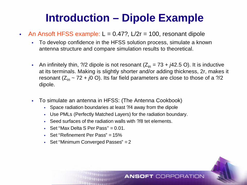
Introduction – Dipole Examplew An Ansoft HFSS example: L = 0.47?, L/2r = 100, resonant dipole
w To develop confidence in the HFSS solution process, simulate a known antenna structure and compare simulation results to theoretical.
w An infinitely thin, ?/2 dipole is not resonant (Zin = 73 + j42.5 O). It is inductive at its terminals. Making is slightly shorter and/or adding thickness, 2r, makes it resonant (Zin ~ 72 + j0 O). Its far field parameters are close to those of a ?/2 dipole.
w To simulate an antenna in HFSS: (The Antenna Cookbook)w Space radiation boundaries at least ?/4 away from the dipolew Use PMLs (Perfectly Matched Layers) for the radiation boundary. w Seed surfaces of the radiation walls with ?/8 tet elements.w Set “Max Delta S Per Pass” = 0.01.w Set “Refinement Per Pass” = 15%w Set “Minimum Converged Passes” = 2
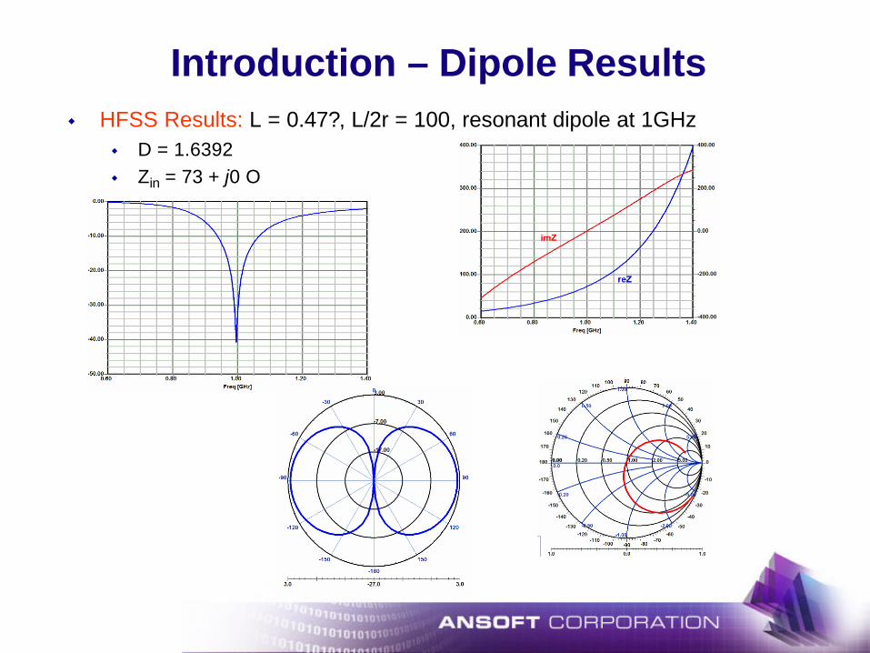
Introduction – Dipole Resultsw HFSS Results: L = 0.47?, L/2r = 100, resonant dipole at 1GHz
w D = 1.6392 w Zin = 73 + j0 O
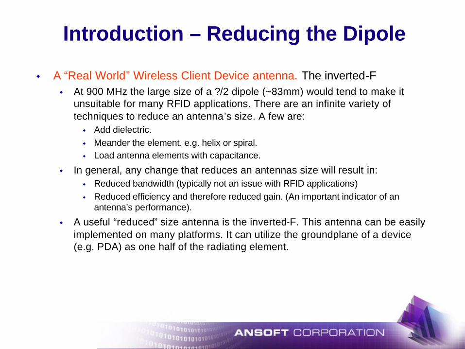
Introduction – Reducing the Dipole
w A “Real World” Wireless Client Device antenna. The inverted-Fw At 900 MHz the large size of a ?/2 dipole (~83mm) would tend to make it
unsuitable for many RFID applications. There are an infinite variety of techniques to reduce an antenna’s size. A few are:w Add dielectric.w Meander the element. e.g. helix or spiral.w Load antenna elements with capacitance.
w In general, any change that reduces an antennas size will result in:w Reduced bandwidth (typically not an issue with RFID applications)w Reduced efficiency and therefore reduced gain. (An important indicator of an
antenna’s performance).
w A useful “reduced” size antenna is the inverted-F. This antenna can be easily implemented on many platforms. It can utilize the groundplane of a device (e.g. PDA) as one half of the radiating element.
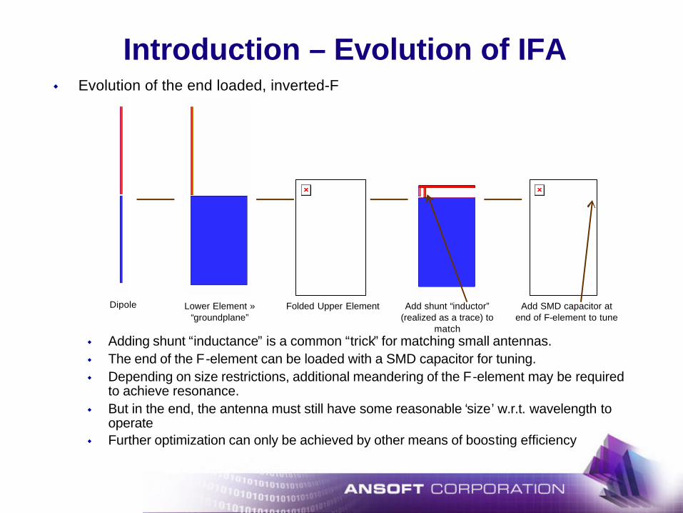
Introduction – Evolution of IFAw Evolution of the end loaded, inverted-F
w Adding shunt “inductance” is a common “trick” for matching small antennas.w The end of the F-element can be loaded with a SMD capacitor for tuning.w Depending on size restrictions, additional meandering of the F-element may be required
to achieve resonance.w But in the end, the antenna must still have some reasonable ‘size’ w.r.t. wavelength to
operatew Further optimization can only be achieved by other means of boosting efficiency
Dipole Lower Element »“groundplane”
Folded Upper Element Add shunt “inductor”(realized as a trace) to
match
Add SMD capacitor at end of F-element to tune
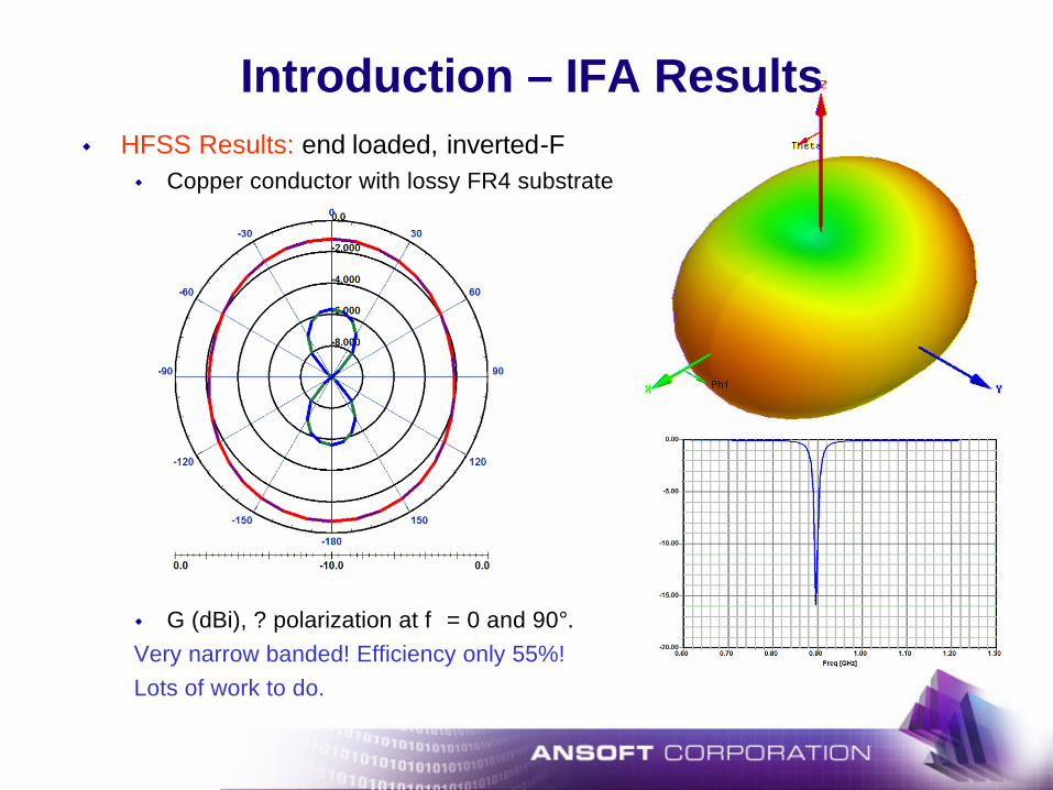
Introduction – IFA Resultsw HFSS Results: end loaded, inverted-F
w Copper conductor with lossy FR4 substrate
w G (dBi), ? polarization at f = 0 and 90°.Very narrow banded! Efficiency only 55%! Lots of work to do.

w Wireless applications growing in complexity, but shrinking in size
w Antenna size reduction comes with consequencesw In general, any change that reduces an antennas size will result
in:w Reduced bandwidth (typically not an issue outside of UWB
applications)w Reduced efficiency and therefore reduced gain. (An important
indicator of an antenna’s performance).w Therefore, engineers must use any and all ‘tools’ at their
disposal for achieving higher performance from smaller antennas, includingw Load tuning – element specificw Folding/Meandering Antenna Topology – element specificw Smart Diversity (Communication System Techniques)w Arraying individually substandard antennas to provide
appropriate coveragew Efficiency improvements by dielectric or other material
loss reduction (dielectric latticing)w Filtering/tuning with FSSw PBG applications for reduction of unwanted imaging
currentsw The remainder of this presentation will focus on simulation
techniques specific to those applications which involve repeated lattice structures and which could be of interest to the Wireless antenna community.
Introduction – Closing Comments

Outlinew Overview of Simulation Approaches for Latticed Structures
w Single/Analytical, Brute, E/H Walls, WG Sim, Linked Boundaries, DomainDecomp
w Overview of Free-space Termination Optionsw Surface impedance, ‘Radiation’, PMLs, Floquet Mode Port
w Simulation Techniques for Electromagnetic Bandgap (EBG) Applicationsw Unit cell approachesw Dispersion and Reflection Analysisw Metallodielectric (FEM/MOM) and Dielectric (FEM)
w Simulation Techniques for FSS Applicationsw Unit Cell Approachesw Excitation Definitionsw FEM and MOM Ramifications (current continuation, etc.)
w Simulation Techniques for Array Applicationsw Unit Cell Approachesw “Active S11” and Scan Blindnessw “Active Element Pattern” extraction methods

Simulation Overview: Analyticalw Analytic array solutions
w Perform isolated single-element experiment
w Apply mathematical array factor
w PROS:w Simple, not computationally intensivew Single-element solution can take
advantage of symmetryw Can be postprocessing step following
any single-element simulationw Easily modified by editing single-
element or array factorw Can include amplitude and phase
variations per element in array factor
w CONS: Idealized Array Results onlyw Neglects Edge Effects (significant in
smaller arrays)w Neglects mutual coupling effects
(significant in most useful arrays)w Cannot predict scan blindness, active
element pattern, active S11
),(element
E ),AF( ),(array
E φθφθφθrr
•=
rrjkN
1nn
neW),AF( •
=∑=θφ
Pattern of single helical element shown at left
Ideal pattern of linear array (10 elements, 1λ spacing, 25° scan angle

Simulation Overview: Brute Forcew Solve entire array in simulationw PROS:
w Permits any phase/amplitude tapers desired
w Works even for ‘defected’arrays
w Neglects Nothing
w CONS:w Computationally very
intensive w Requires setting all sources
independentlyw Unless feed network included
in array geometry
w Impractical for physically or ‘geometrically’ very large arrays
Linear-phase fed 16 x 16 patch antenna array. Solvable in Ansoft Designer PlanarEM (MoM) simulation
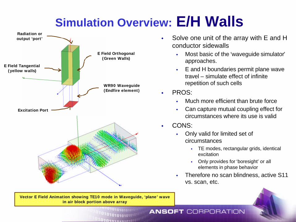
Simulation Overview: E/H Wallsw Solve one unit of the array with E and H
conductor sidewallsw Most basic of the ‘waveguide simulator’
approaches. w E and H boundaries permit plane wave
travel – simulate effect of infinite repetition of such cells
w PROS:w Much more efficient than brute forcew Can capture mutual coupling effect for
circumstances where its use is valid
w CONS:w Only valid for limited set of
circumstancesw TE modes, rectangular grids, identical
excitationw Only provides for ‘boresight’ or all
elements in phase behavior
w Therefore no scan blindness, active S11 vs. scan, etc.
WR90 Waveguide (Endfire element)
E Field Orthogonal (Green Walls)
E Field Tangential (yellow walls)
Excitation Port
Radiation or output ‘port’
Vector E Field Animation showing TE10 mode in Waveguide, ‘plane’ wave in air block portion above array

Simulation Overview: “Waveguide Simulator”w Solve one unit of the array with various
combinations of E and H conductor sidewalls (‘waveguide’)w Solve many ‘modes’ of excitation for the
output port.w Each ‘mode’ coincides with a specific
angle of incidence, e.g. scan angle out of the array
w PROS:w Much more efficient than brute forcew Can capture mutual coupling effect over
specific discrete scan anglesw CONS:
w Only valid for discrete scan angles and modes
w User must compute modal to angle relationshipsw Relative to array spacing, etc.
w No continuous scan blindness, active S11 vs scan angle.
w Pattern computation from results difficult (output is S-parameters)
Example linearly taper slot antenna :
•Length = 1.38 cm
•Opening = 1.52 cm
•Substrate
•Thickness = 0.1cm
•er = 2.2
•Unit cell: 2.215cm x 4.78cm
•Analyzed 3.8-5.6 GHz.
Co
nd
uct
ive
Wal
ls
Excitation Port
Output WG ‘port’
Results Compare to [2]. Further Details on WG
Simulation in [3]
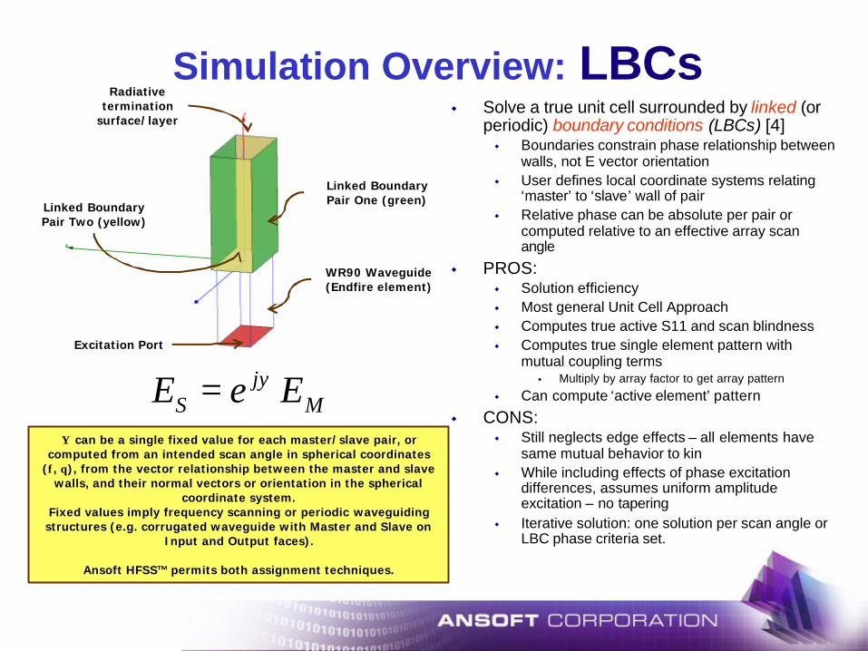
Simulation Overview: LBCsw Solve a true unit cell surrounded by linked (or
periodic) boundary conditions (LBCs) [4]w Boundaries constrain phase relationship between
walls, not E vector orientationw User defines local coordinate systems relating
‘master’ to ‘slave’ wall of pairw Relative phase can be absolute per pair or
computed relative to an effective array scan angle
w PROS:w Solution efficiencyw Most general Unit Cell Approachw Computes true active S11 and scan blindnessw Computes true single element pattern with
mutual coupling termsw Multiply by array factor to get array pattern
w Can compute ‘active element’ pattern
w CONS:w Still neglects edge effects – all elements have
same mutual behavior to kinw While including effects of phase excitation
differences, assumes uniform amplitude excitation – no tapering
w Iterative solution: one solution per scan angle or LBC phase criteria set.
WR90 Waveguide (Endfire element)
Linked BoundaryPair One (green)
Excitation Port
Radiativetermination
surface/layer
Linked BoundaryPair Two (yellow)
Mj
S EeE ψ=Ψ can be a single fixed value for each master/slave pair, or
computed from an intended scan angle in spherical coordinates (φ, θ), from the vector relationship between the master and slave
walls, and their normal vectors or orientation in the spherical coordinate system.
Fixed values imply frequency scanning or periodic waveguidingstructures (e.g. corrugated waveguide with Master and Slave on
Input and Output faces).
Ansoft HFSS™ permits both assignment techniques.
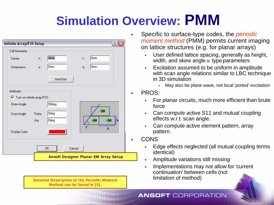
Simulation Overview: PMMw Specific to surface-type codes, the periodic
moment method (PMM) permits current imaging on lattice structures (e.g. for planar arrays)w User defined lattice spacing, generally as height,
width, and skew angle α type parametersw Excitation assumed to be uniform in amplitude
with scan angle relations similar to LBC technique in 3D simulationw May also be plane wave, not local ‘ported’ excitation
w PROS:w For planar circuits, much more efficient than brute
forcew Can compute active S11 and mutual coupling
effects w.r.t. scan angle. w Can compute active element pattern, array
pattern.w CONS
w Edge effects neglected (all mutual coupling terms identical)
w Amplitude variations still missingw Implementations may not allow for ‘current
continuation’ between cells (not limitation of method)
Ansoft Designer Planar EM Array Setup
Detailed Description of the Periodic Moment Method can be found in [5].

Simulation Overview: Domain Decompositionw Subdivide model into ‘subdomains’ of
unique behavior, and solve each iteratively to determine interaction between subdomain boundariesw Domains can be identical geometry in non-
identical placements, e.g. array corner, edge, and center elements
w PROs:w Solution efficiency better than brute forcew Computes true active S11 and scan
blindnessw Compute all array behavior including scan
blindness, active S11, active element pattern, and array pattern including both mutual coupling AND edge effects
w Useful for other large-structure applications besides periodic geometries (see bottom)
w Can set excitations for amplitude as well as phase offsets (Taylor taper, etc.)
w CONsw Iteration between subdomains reduces
efficiency slightly below that of LBC approach
w Excitations now individually managedw No known commercial software
currently has this technique
Conceptual array with sub-domains color-coded.
Rothman Lens (Ansoft, under development)

Simulation Overview: Final Wordsw As discussed, each method has its benefits and drawbacksw As a general rule, the fewer the drawbacks, the more usage-intensive a
technique will becomew E.g. LBC’s requiring local coordinates, PMM requiring lattice definitions, Domain
Decomposition requiring segregation of subdomains.w Misuse (incorrect sizing of unit cell as compared to array factor to be applied later)
will result in nonphysical results
w For different applications, different methods may prove more useful than othersw E.g. PMM for planar geometries vs. LBCs for more volumetric ones
w Remainder of course will apply a subset of these methods for specific applicationsw Use of Periodic Moment Method will be illustrated for FSS and PBG applications
using Ansoft Designer (Planar EM level solver)w Use of Linked Boundary Condition method will be illustrated for FSS, PBG, and
array applications using Ansoft HFSS
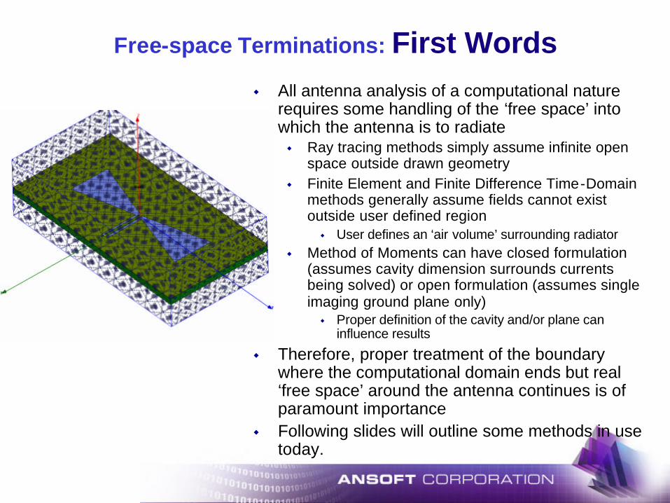
Free-space Terminations: First Wordsw All antenna analysis of a computational nature
requires some handling of the ‘free space’ into which the antenna is to radiatew Ray tracing methods simply assume infinite open
space outside drawn geometryw Finite Element and Finite Difference Time-Domain
methods generally assume fields cannot exist outside user defined regionw User defines an ‘air volume’ surrounding radiator
w Method of Moments can have closed formulation (assumes cavity dimension surrounds currents being solved) or open formulation (assumes single imaging ground plane only)w Proper definition of the cavity and/or plane can
influence results
w Therefore, proper treatment of the boundary where the computational domain ends but real ‘free space’ around the antenna continues is of paramount importance
w Following slides will outline some methods in use today.

Free-space Terminations: 377Ωw Intrinsic impedance of free space is given as
w Therefore, the ‘simplest’ way to terminate a volume with the implication of further free space outside it is with a 377 Ω/? surface impedancew “Ω/? “ denotes “ohms per square” which is generalized sheet resistance, not to be mistaken as having
any ‘unit’ (such as meters2) implicationsw For conversion, imagine a thin film resistor, l long (direction of current flow) by w wide. Lumped
resistance is related to sheet resistance by
w For a coaxial resistor (annular surface area with inner radius a and outer b) the relation would be:
(derivation left to the student )
w PROS: Simple to assign; single-value entry; works for eigensolutions too w CONS: What about terminating volumes other than vacuum? Boundaries between volumes?
Ω≈== 37773031.376o
oo ε
µη
Rsab
RL
= ln
Rslw
RL =

Free-space Terminations: “Radiation Boundary”
w Most 3D simulation software uses a second-order impedance surface termed a “radiation boundary”
w Unlike simple 377 Ω, a radiation boundary is computed for each material touching the surface and is frequency dependent
w PROS:w Superior absorption to single-valued impedance boundary, especially with nonhomogeneous
volumesw Reasonably absorptive with reflections exceeding 80 dB isolation possiblew Transparent user setup (ease of use)
w CONS:w As a surface termination only, sensitive to angle of incidence and distance from radiatorw Loses some absorption over broad solution frequency ranges using numerical sweep techniques
(e.g. AWE, ALPS)w Not functional for eigensolution due to frequency dependence! (ko is wavenumber ω√µε )
( ) ( ) ( )tantantantantantantantan Ekj
Ekj
EjkEoo
o •∇∇+×∇×∇−=×∇
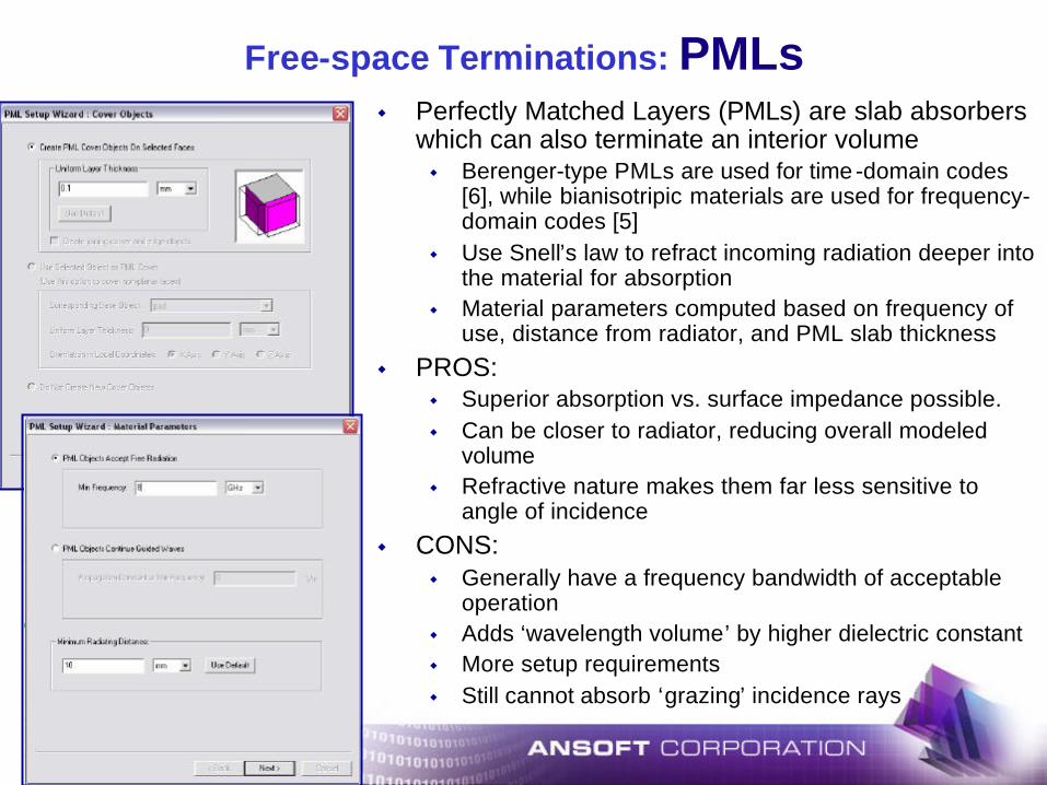
Free-space Terminations: PMLsw Perfectly Matched Layers (PMLs) are slab absorbers
which can also terminate an interior volumew Berenger-type PMLs are used for time -domain codes
[6], while bianisotripic materials are used for frequency-domain codes [5]
w Use Snell’s law to refract incoming radiation deeper into the material for absorption
w Material parameters computed based on frequency of use, distance from radiator, and PML slab thickness
w PROS:w Superior absorption vs. surface impedance possible.w Can be closer to radiator, reducing overall modeled
volumew Refractive nature makes them far less sensitive to
angle of incidence
w CONS:w Generally have a frequency bandwidth of acceptable
operationw Adds ‘wavelength volume’ by higher dielectric constantw More setup requirementsw Still cannot absorb ‘grazing’ incidence rays
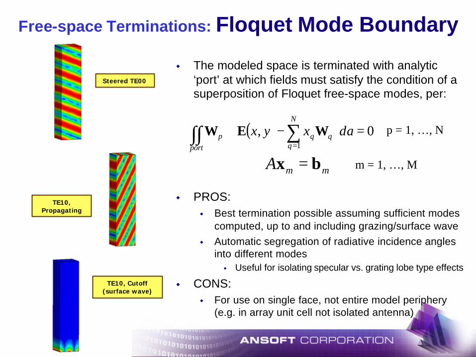
Free-space Terminations: Floquet Mode Boundary
w The modeled space is terminated with analytic ‘port’ at which fields must satisfy the condition of a superposition of Floquet free-space modes, per:
w PROS:w Best termination possible assuming sufficient modes
computed, up to and including grazing/surface wavew Automatic segregation of radiative incidence angles
into different modesw Useful for isolating specular vs. grating lobe type effects
w CONS:w For use on single face, not entire model periphery
(e.g. in array unit cell not isolated antenna)
( ) 0,1
=
−⋅∫∫ ∑
=
daxyxport
N
qqqp WEW
mmA bx =
p = 1, …, N
m = 1, …, M
Steered TE00
TE10, Propagating
TE10, Cutoff (surface wave)

Terminations: Final Wordsw As discussed, each method has its benefits and drawbacksw As a general rule, the fewer the drawbacks, the more usage-intensive a
technique will becomew PMLs require additional setup yet provide superior absorptionw Floquet boundaries require additional computational requirementsw Additional setup may be made transparent to users with commercial software
advancesw But ‘assumptions’ made should always be understood by educated users!!
w For different applications, different methods may prove more useful than othersw E.g. Floquet mode terminations not generally usable for non-arrayed element
analysisw Sometimes ‘easiest method’ is ‘enough’
w Remainder of course will apply a subset of these methods for specific applicationsw Use of Radiation Boundary, 377 ohm Impedance, or PMLs will be illustrated as
applicable for examples from Ansoft HFSS™w Examples shown from Ansoft Designer™ Planar EM solver use ‘open’ formulation
Method of Moments (MoM)

Part Two: Specific Application Techniques for EBGs
Wireless and Microwave Technology ConferenceTutorial Session RA-2
Thursday, April 07, 2005Clearwater, FL

Electromagnetic Bandgaps (EBGs): Description
w Electromagnetic Bandgaps (EBGs) formerly called Photonic Bandgaps (PBGs) are an interesting new technique for surface wave reduction in antenna applicationsw A periodic metal pattern or dielectric change
provides a tuned circuit effect with a ‘forbidden band’, preventing surface wave transmission
w At the tuned frequency, the surface has a ‘high impedance’ effect [7]
w Therefore, unlike a ground plane, it reflects incoming waves in phase rather than 180° out of phase
w Implication:w Ground plane imaging currents will not be
destructively interfering with desired antenna behavior
w Balanced elements can be made much closer to such a surface without efficiency penalties, rather than requiring cavities or voids beneathw NOT for use ‘beneath’ patch-like antennas
Dielectric rod EBG (top) and Sievenpiperhexagonal plates with via (bottom, [7])

EBGs: Characteristics for Analysisw The features of an EBG construction of interest
to antenna designers are:w Dispersion Diagram – wave propagation vs.
frequency, also known as the ‘band diagram’w Will show the frequency band(s) over which the
EBG forbids surface wave travel
w Reflection Phase Analysis clarifies the subset of the band gap where the surface reflection is constructive (±90° phase range)
w Both behaviors are an array or lattice phenomenon, and will not show up for a single or even small number of elements
w Useful EBGs will have feature size much smaller than wavelengthw Otherwise they’re too large to assist with a small
antenna design
w Therefore, solving a ‘brute force’ array of such features would become computationally demandingw “Geometrically Dense” – much discretizationw Perfect application for the Unit Cell Techniques
discussed so far
phase1 = 0
phase2 = 0 - 180º
phase1 = 0 - 180º
phase2 = 180º
phase1 = phase2
= 180º - 0
∫∫
•
•=
S
S scattered
PBGdss
dsEPhase
ˆ
)(φ
( ) 180
360180
+−=∆
⋅−=
platePBG
plated
φφφ
λφ
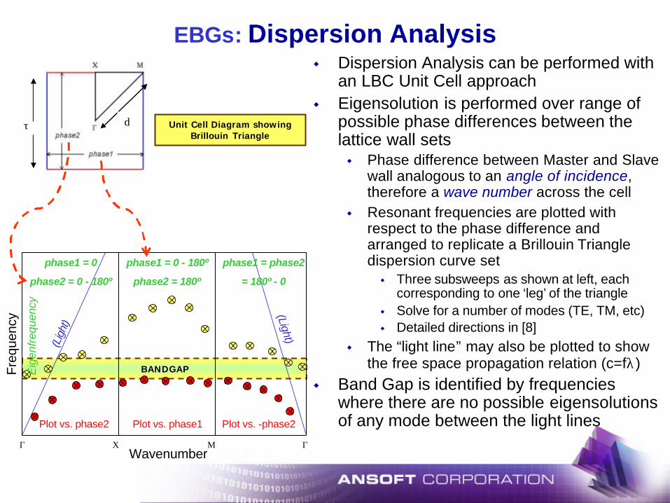
EBGs: Dispersion Analysisw Dispersion Analysis can be performed with
an LBC Unit Cell approachw Eigensolution is performed over range of
possible phase differences between the lattice wall setsw Phase difference between Master and Slave
wall analogous to an angle of incidence, therefore a wave number across the cell
w Resonant frequencies are plotted with respect to the phase difference and arranged to replicate a Brillouin Triangle dispersion curve setw Three subsweeps as shown at left, each
corresponding to one ‘leg’ of the trianglew Solve for a number of modes (TE, TM, etc)w Detailed directions in [8]
w The “light line” may also be plotted to show the free space propagation relation (c=fλ)
w Band Gap is identified by frequencies where there are no possible eigensolutionsof any mode between the light lines
dτ Unit Cell Diagram showing Brillouin Triangle
BANDGAP
Γ Χ Μ Γ
Fre
quen
cy
(Lig
ht)
(Light)
phase1 = 0
phase2 = 0 - 180º
Wavenumber
phase1 = 0 - 180º
phase2 = 180º
phase1 = phase2
= 180º - 0
Plot vs. phase2 Plot vs. phase1 Plot vs. -phase2
Eig
enfr
eque
ncy
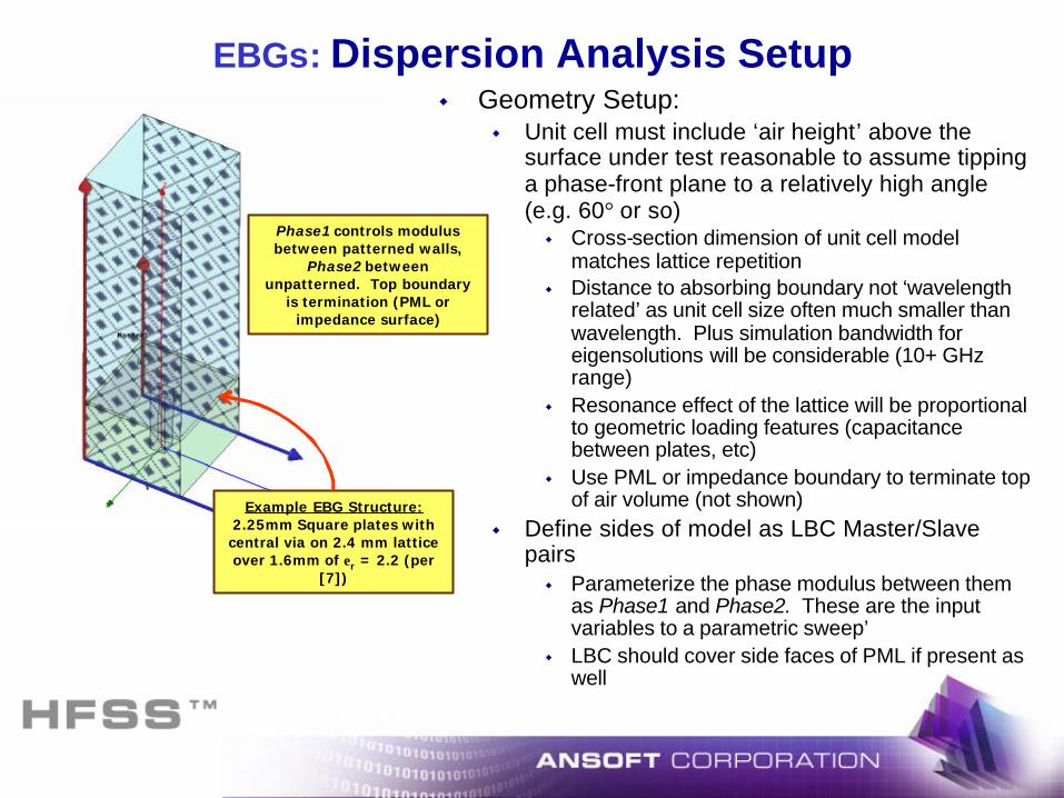
EBGs: Dispersion Analysis Setupw Geometry Setup:
w Unit cell must include ‘air height’ above the surface under test reasonable to assume tipping a phase-front plane to a relatively high angle (e.g. 60° or so)w Cross-section dimension of unit cell model
matches lattice repetitionw Distance to absorbing boundary not ‘wavelength
related’ as unit cell size often much smaller than wavelength. Plus simulation bandwidth for eigensolutions will be considerable (10+ GHz range)
w Resonance effect of the lattice will be proportional to geometric loading features (capacitance between plates, etc)
w Use PML or impedance boundary to terminate top of air volume (not shown)
w Define sides of model as LBC Master/Slave pairsw Parameterize the phase modulus between them
as Phase1 and Phase2. These are the input variables to a parametric sweep’
w LBC should cover side faces of PML if present as well
Phase1 controls modulus between patterned walls,
Phase2 between unpatterned. Top boundary
is termination (PML or impedance surface)
Example EBG Structure:2.25mm Square plates with
central via on 2.4 mm lattice over 1.6mm of εr = 2.2 (per
[7])

EBGs: Dispersion Analysis Outputsw Solution Techniques:
w Simulation convergence can be aided with the use of mesh operations or user-assisted instructionsw Adaptive mesh techniques will converge
on proper fields regardless. But if user has insight into expected behavior, such as importance of the narrow gap between plates from cell to cell, providing instruction to pre-condition the mesh can speed the solution process.
w Results:w After simulation, results can be plotted as
data table or as graphical formw Eigenmodes fall into curves, between
which will be the band gapw Analytical values such as the light line can
be superposed on the same axes using Output Variable capability.
w Results from one leg of the BrillouinTriangle are shown at right, indicating an expected bandgapw Gap of ~11-17 GHz agrees with
Ref [7] paper
Note denser mesh at cell periphery (gap between
plates)
BANDGAP
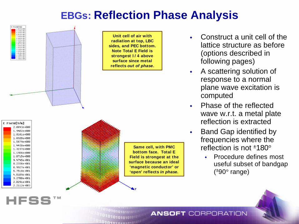
EBGs: Reflection Phase Analysis
w Construct a unit cell of the lattice structure as before (options described in following pages)
w A scattering solution of response to a normal plane wave excitation is computed
w Phase of the reflected wave w.r.t. a metal plate reflection is extracted
w Band Gap identified by frequencies where the reflection is not ±180°w Procedure defines most
useful subset of bandgap(±90° range)
Unit cell of air with radiation at top, LBC
sides, and PEC bottom. Note Total E Field is strongest λ/4 above surface since metal
reflects out of phase.
Same cell, with PMC bottom face. Total E
Field is strongest at the surface because an ideal ‘magnetic conductor’ or ‘open’ reflects in phase.
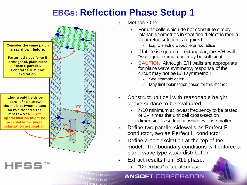
EBGs: Reflection Phase Setup 1w Method One
w For unit cells which do not constitute simply ‘planar’ geometries in stratified dielectric media, volumetric solution is required. w E.g. Dielectric woodpile or rod lattice
w If lattice is square or rectangular, the E/H wall “waveguide simulator” may be sufficient
w CAUTION: Although E/H walls are appropriate for plane wave symmetry, response of the circuit may not be E/H symmetric!!w See example at leftw May limit polarization cases for this method
w Construct unit cell with reasonable height above surface to be evaluatedw λ/10 minimum at lowest frequency to be tested,
or 3-4 times the unit cell cross-section dimension is sufficient, whichever is smaller
w Define two parallel sidewalls as Perfect E conductor, two as Perfect H conductor
w Define a port excitation at the top of the model. The boundary conditions will enforce a plane-wave type wave distribution
w Extract results from S11 phase.w “De-embed” to top of surface
Consider the same patch array shown before.
Patterned sides force E orthogonal, plain sides
force E parallel. Generates TEM port
excitation.
…but would fields be ‘parallel’ to narrow
channels between plates on two sides vs. the other two? NO. Yet
approximation might be acceptable for single
polarization assumption. ??
??
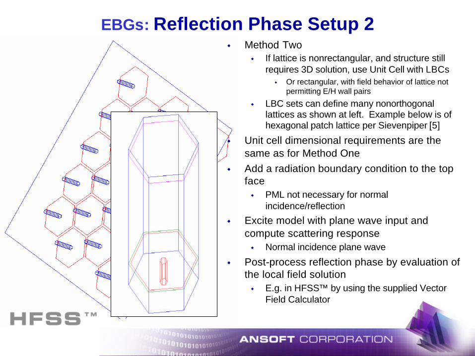
EBGs: Reflection Phase Setup 2w Method Two
w If lattice is nonrectangular, and structure still requires 3D solution, use Unit Cell with LBCsw Or rectangular, with field behavior of lattice not
permitting E/H wall pairs
w LBC sets can define many nonorthogonallattices as shown at left. Example below is of hexagonal patch lattice per Sievenpiper [5]
w Unit cell dimensional requirements are the same as for Method One
w Add a radiation boundary condition to the top facew PML not necessary for normal
incidence/reflection
w Excite model with plane wave input and compute scattering responsew Normal incidence plane wave
w Post-process reflection phase by evaluation of the local field solutionw E.g. in HFSS™ by using the supplied Vector
Field Calculator

EBGs: Reflection Phase Setup 3w For ‘planar’ circuit, can
take advantage of method of moments and solve unit cell in PMM
w Draw single unit metal pattern in layoutw Depending on treatment
of current continuation in your code of choice, consider if pattern cell should be connected or not
w Define lattice constants for array
w Specify plane wave excitation and frequencies of solution.w Normal direction onlyw Multiple polarizations if
desiredSetup steps shown for planar EBG simulation using Ansoft Designer.
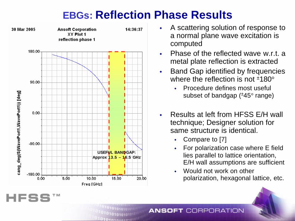
EBGs: Reflection Phase Resultsw A scattering solution of response to
a normal plane wave excitation is computed
w Phase of the reflected wave w.r.t. a metal plate reflection is extracted
w Band Gap identified by frequencies where the reflection is not ±180°w Procedure defines most useful
subset of bandgap (±45° range)
w Results at left from HFSS E/H wall technique; Designer solution for same structure is identical.w Compare to [7]w For polarization case where E field
lies parallel to lattice orientation, E/H wall assumptions are sufficient
w Would not work on other polarization, hexagonal lattice, etc.
USEFUL BANDGAP:Approx 13.5 – 16.5 GHz
Part Three: Specific Application Techniques for FSSs
Wireless and Microwave Technology ConferenceTutorial Session RA-2
Thursday, April 07, 2005Clearwater, FL
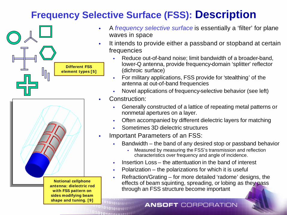
Frequency Selective Surface (FSS): Descriptionw A frequency selective surface is essentially a ‘filter’ for plane
waves in spacew It intends to provide either a passband or stopband at certain
frequenciesw Reduce out-of-band noise; limit bandwidth of a broader-band,
lower-Q antenna, provide frequency-domain ‘splitter’ reflector (dichroic surface)
w For military applications, FSS provide for ‘stealthing’ of the antenna at out-of-band frequencies
w Novel applications of frequency-selective behavior (see left)w Construction:
w Generally constructed of a lattice of repeating metal patterns or nonmetal apertures on a layer.
w Often accompanied by different dielectric layers for matchingw Sometimes 3D dielectric structures
w Important Parameters of an FSS:w Bandwidth – the band of any desired stop or passband behavior
w Measured by measuring the FSS’s transmission and reflection characteristics over frequency and angle of incidence.
w Insertion Loss – the attentuation in the band of interestw Polarization – the polarizations for which it is usefulw Refraction/Grating – for more detailed ‘radome’ designs, the
effects of beam squinting, spreading, or lobing as they pass through an FSS structure become important
Notional cellphoneantenna: dielectric rod
with FSS pattern on sides modifying beam shape and tuning. [9]
Different FSS element types [5]

FSS: Nonplanar Cell Analysis 1w Using a volumetric code like HFSS™, set up unit
cell model with linked boundary conditionsw E/H walls also useable for limited cases (normal
incidence only, rectangular lattice)
w Source excitation is plane wave at angle (φ,θ)w Can be varied in parametric fashion for analysis w.r.t.
incidence angle
w LBC boundary setup uses “scan angle” of (φ+180°,θ)w Boundary condition reinforces ‘specular’ reflection
direction
w FSS is a transmissive surface so unit cell requires radiation termination of some form on both top andbottom of modeled cell!w Radiation boundaries or even simple 377 Ω sufficient
for normal incidence casew But FSS analysis implies angle of incidence range as
well as frequency range of interest. Therefore more robust absorption offered by PML and/or Floquet ports are preferred
PML
PML
Incoming Eval S
Outgoing Eval S
More details of FSS analysis using HFSS
can be found in [10].
Non-rectangular lattice of
incompletely dielectric-filled holes in thick metal plate. This type of FSS is
used in some avionics applications
due to high structural strength.

FSS: Nonplanar Cell Analysis 2w Results extracted from scattered and total field data
w Integration surfaces drawn into model (inner face of PML or interior to ‘air’ height between PML and FSS)
w Integrate Poynting vector flux on evaluation surfaces
w Integration of Total fields on outgoing side provides Transmitted power.
w Integration of Scattered fields on incoming side provides Reflected power.
w Integration of Incident fields on either plane provides Incident power.
w Ratios of above provide transmission and reflection coefficients
w HFSS™v10 has automated these post-processing routines as if they are S-parameters
Notional cellphoneantenna: dielectric rod
with FSS pattern on sides modifying beam
shape and tuning. [12]
=
⋅×=
⋅×=
∫
∫∗
∗
i
t
s
incinci
s
tottott
PP
T
dsHEP
dsHEP
log10
Evaluation planes for
integration of power flux
(unnecessary in HFSS™v10)
PML
PML
Incoming Eval S
Outgoing Eval S
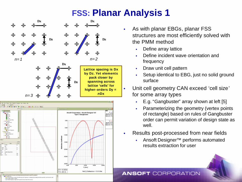
FSS: Planar Analysis 1
w As with planar EBGs, planar FSS structures are most efficiently solved with the PMM methodw Define array latticew Define incident wave orientation and
frequencyw Draw unit cell patternw Setup identical to EBG, just no solid ground
surface
w Unit cell geometry CAN exceed ‘cell size’for some array typesw E.g. “Gangbuster” array shown at left [5]w Parameterizing the geometry (vertex points
of rectangle) based on rules of Gangbuster order can permit variation of design state as well.
w Results post-processed from near fieldsw Ansoft Designer™ performs automated
results extraction for user
Dx
Dz
Dx
Dz
Dx
Dz
n=1 n=2
n=3
Lattice spacing is Dxby Dz. Yet elements
pack closer by spanning across lattice ‘cells’ for
higher-orders Dy = nDx

FSS: Planar Analysis 2 – Gangbusters, cont.
Example results of additional
Gangbuster Arrays. Higher order results in flatter reflection coefficient out of
band, slight reduction in resonant
frequency. Per [5]

FSS: Planar Analysis 3 – Current Continuation
w While unit cell ‘geometry’ can extend beyond lattice, metal may not be permitted to ‘connect’between cellsw PMM method implementation may or may not
include the effects of ‘current continuation’between cells
w Example at left – ring array does not touch. Inductive grid screen, however, does.
w In MoM simulators which permit magneticcurrent modeling, drawing cell pattern as ‘negative’ on a ‘ground plane’ layer provides easy workaroundw Rather than drawing the inductive grid on a
‘trace’ layer, draw the holes in the grid on a ‘plane’ layer
w Magnetic current in each cell is confined and does not continue

Part Four: Specific Application Techniques for Antenna Arrays
Wireless and Microwave Technology ConferenceTutorial Session RA-2
Thursday, April 07, 2005Clearwater, FL
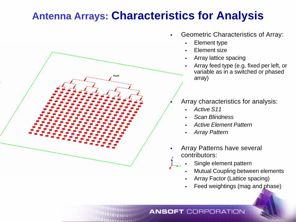
Antenna Arrays: Characteristics for Analysisw Geometric Characteristics of Array:
w Element typew Element sizew Array lattice spacingw Array feed type (e.g. fixed per left, or
variable as in a switched or phased array)
w Array characteristics for analysis:w Active S11w Scan Blindnessw Active Element Patternw Array Pattern
w Array Patterns have several contributors:w Single element patternw Mutual Coupling between elementsw Array Factor (Lattice spacing)w Feed weightings (mag and phase)
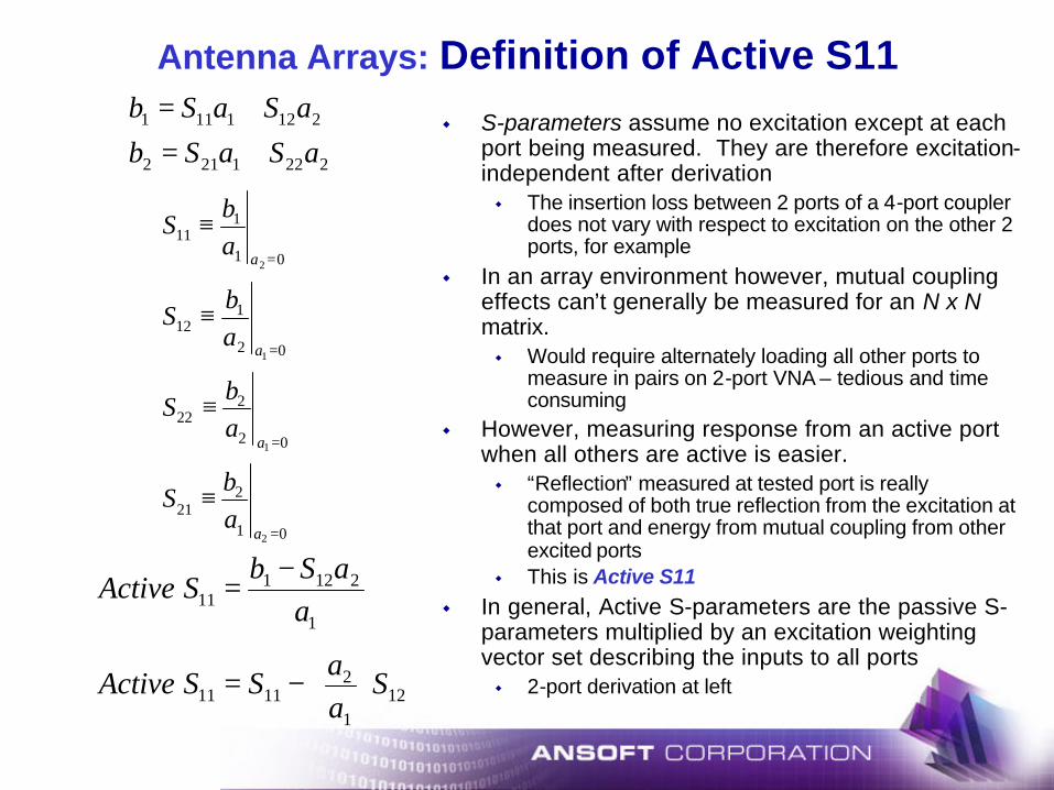
Antenna Arrays: Definition of Active S11w S-parameters assume no excitation except at each
port being measured. They are therefore excitation-independent after derivationw The insertion loss between 2 ports of a 4-port coupler
does not vary with respect to excitation on the other 2 ports, for example
w In an array environment however, mutual coupling effects can’t generally be measured for an N x N matrix.w Would require alternately loading all other ports to
measure in pairs on 2-port VNA – tedious and time consuming
w However, measuring response from an active port when all others are active is easier.w “Reflection” measured at tested port is really
composed of both true reflection from the excitation at that port and energy from mutual coupling from other excited ports
w This is Active S11w In general, Active S-parameters are the passive S-
parameters multiplied by an excitation weighting vector set describing the inputs to all portsw 2-port derivation at left
01
221
02
222
02
112
01
111
2
1
1
2
=
=
=
=
≡
≡
≡
≡
a
a
a
a
ab
S
ab
S
ab
S
ab
S
2221212
2121111
aSaSbaSaSb
+=+=
121
21111
1
212111
Saa
SSActive
aaSb
SActive
−=
−=

Antenna Arrays: Definition of Scan Blindnessw As an array beam is scanned to greater
and greater angles from boresight, mutual coupling will eventually generate so much “reflection” cross-fed into adjacent elements that the array is no longer usablew Effect is not simply gradual degradation off
boresight but may have strong interaction at specific angles
w This characteristic is obviously related to Active S11w As Active S11 increases, more and more
power is being coupled back toward the transmitter in adjacent elements and not radiated
w Therefore a plot of Active S11 with respect to excitation vector sets representing increasing beam scan angles will display
w Scan Blindness is defined as the angles over which an array is ‘blind’ because mutual coupling effects prevent scanning of a usable pattern in that directionw If you can’t transmit in that direction, neither
can you receive due to reciprocity
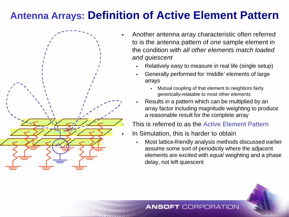
Antenna Arrays: Definition of Active Element Pattern
w Another antenna array characteristic often referred to is the antenna pattern of one sample element in the condition with all other elements match loaded and quiescentw Relatively easy to measure in real life (single setup)w Generally performed for ‘middle’ elements of large
arraysw Mutual coupling of that element to neighbors fairly
generically-relatable to most other elements
w Results in a pattern which can be multiplied by an array factor including magnitude weighting to produce a reasonable result for the complete array
w This is referred to as the Active Element Patternw In Simulation, this is harder to obtain
w Most lattice-friendly analysis methods discussed earlier assume some sort of periodicity where the adjacent elements are excited with equal weighting and a phase delay, not left quiescent
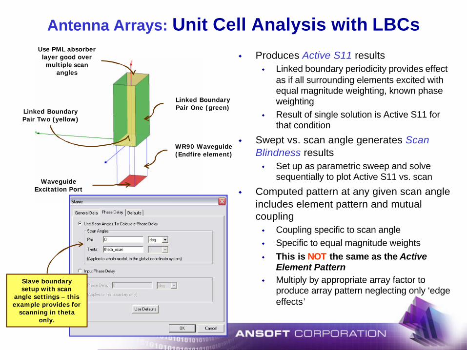
Antenna Arrays: Unit Cell Analysis with LBCs
w Produces Active S11 resultsw Linked boundary periodicity provides effect
as if all surrounding elements excited with equal magnitude weighting, known phase weighting
w Result of single solution is Active S11 for that condition
w Swept vs. scan angle generates Scan Blindness resultsw Set up as parametric sweep and solve
sequentially to plot Active S11 vs. scan
w Computed pattern at any given scan angle includes element pattern and mutual couplingw Coupling specific to scan anglew Specific to equal magnitude weightsw This is NOT the same as the Active
Element Patternw Multiply by appropriate array factor to
produce array pattern neglecting only ‘edge effects’
WR90 Waveguide (Endfire element)
Linked BoundaryPair One (green)
Use PML absorber layer good over
multiple scan angles
Linked BoundaryPair Two (yellow)
Waveguide Excitation Port
Slave boundary setup with scan
angle settings – this example provides for
scanning in theta only.

Antenna Arrays: Example Array Results
w Example JRM Array [4]w WR-90 endfire in rectangular arrayw 0.5 x 1.0 inch latticew Scannable in E or H plane. Example is E-
plane scanning.
w Results demonstrate Active S11 vs. E-plane Scanningw Reasonable match at boresight (endfire
WGs do couple) improves with some scanning
w 40 degrees is ‘optimum’ scan angle.w Return Loss breaks -10 dB at about 67
degrees scan angle, indicating effective Scan Blindness beginning about here.
w Similar scans of both phi and theta simultaneously can demonstrate loss of scanning earlier at the ‘corners’ (e.g. can scan further in phi or theta when other angle is non-scanned)
WR90 WG in 0.5 x 1 inch lattice. Scanned in E-plane from 0 –
90 degrees. Animation at left shows 40 degree
scan angle
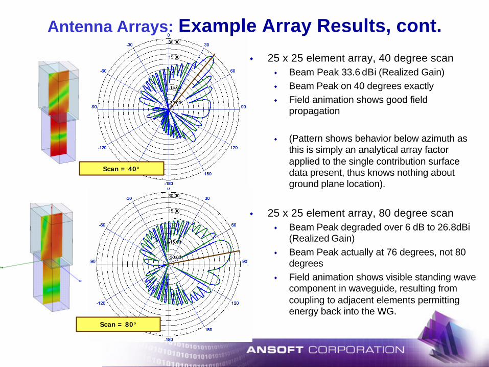
Antenna Arrays: Example Array Results, cont.
w 25 x 25 element array, 40 degree scanw Beam Peak 33.6 dBi (Realized Gain)w Beam Peak on 40 degrees exactlyw Field animation shows good field
propagation
w (Pattern shows behavior below azimuth as this is simply an analytical array factor applied to the single contribution surface data present, thus knows nothing about ground plane location).
w 25 x 25 element array, 80 degree scanw Beam Peak degraded over 6 dB to 26.8dBi
(Realized Gain)w Beam Peak actually at 76 degrees, not 80
degreesw Field animation shows visible standing wave
component in waveguide, resulting from coupling to adjacent elements permitting energy back into the WG.
Scan = 40°
Scan = 80°
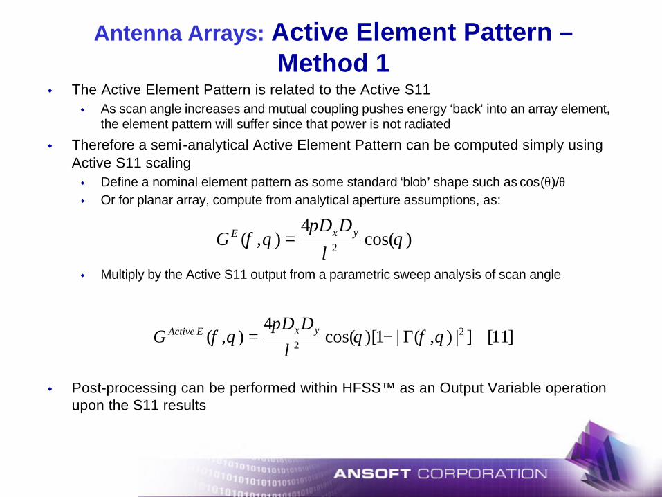
Antenna Arrays: Active Element Pattern –Method 1
w The Active Element Pattern is related to the Active S11w As scan angle increases and mutual coupling pushes energy ‘back’ into an array element,
the element pattern will suffer since that power is not radiated
w Therefore a semi-analytical Active Element Pattern can be computed simply using Active S11 scalingw Define a nominal element pattern as some standard ‘blob’ shape such as cos(θ)/θw Or for planar array, compute from analytical aperture assumptions, as:
w Multiply by the Active S11 output from a parametric sweep analysis of scan angle
w Post-processing can be performed within HFSS™ as an Output Variable operation upon the S11 results
)cos(4
),( 2 θλ
πθφ yxE DD
G =
]11[]|),(|1)[cos(4
),( 22 θφθ
λπ
θφ Γ−= yxEActive DDG
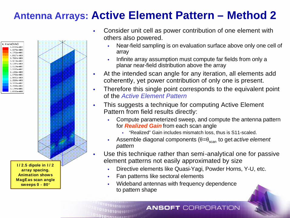
Antenna Arrays: Active Element Pattern – Method 2w Consider unit cell as power contribution of one element with
others also powered.w Near-field sampling is on evaluation surface above only one cell of
arrayw Infinite array assumption must compute far fields from only a
planar near-field distribution above the arrayw At the intended scan angle for any iteration, all elements add
coherently, yet power contribution of only one is present.w Therefore this single point corresponds to the equivalent point
of the Active Element Patternw This suggests a technique for computing Active Element
Pattern from field results directly:w Compute parameterized sweep, and compute the antenna pattern
for Realized Gain from each scan anglew “Realized” Gain includes mismatch loss, thus is S11-scaled.
w Assemble diagonal components (θ=θscan to get active element pattern
w Use this technique rather than semi-analytical one for passive element patterns not easily approximated by sizew Directive elements like Quasi-Yagi, Powder Horns, Y-U, etc.w Fan patterns like sectoral elementsw Wideband antennas with frequency dependence
to pattern shape
λ/2.5 dipole in λ/2 array spacing.
Animation shows MagE as scan angle
sweeps 0 - 80°

Antenna Arrays: Active Element Example
w Classic Pozar paper [11] derives relationships for Active Element Pattern from base principles
w Uses dipole antenna as examplew Shown prior page
w Construct unit-cell pattern in HFSS and compare to supplied plot of linear gain vs. scan angle in E-planew Paper references all dimensions with
respect to wavelengthw Select one such configuration and
simulate

Antenna Arrays: HFSS Projectw HFSS Project constructed to match that in
the paper as best as possiblew Arbitrarily picked 3 GHz solution for easy
wavelength (100 mm)w λ/30 used as dipole ‘width’. w No dipole length given, arbitrary length of
λ/2.5 selected to fit inside λ/2.5 unit cellw Linked Boundary Conditions applied on sides
w Lumped port placed in center, 50 Ωnormalized
w Substrate constructed to appropriate thickness and εr = 2.55 per reference
w Air height left at 150mm, 50mm thick PML constructed on top
w Dipole aligned parallel to Y axis, so “E-plane”is φ=90, θ varying.
w Parametric sweep requested for scan angle of every 2° from θ = 0 to 80°

Antenna Arrays: HFSS Raw ResultsRealized Gain vs.
Theta for each Scan angle (dB). One point
of each curve contributes to Active
Element Pattern.
Same data, tabular format, linear (not
dB). Can right-click data table for easy export to Excel or other programs.
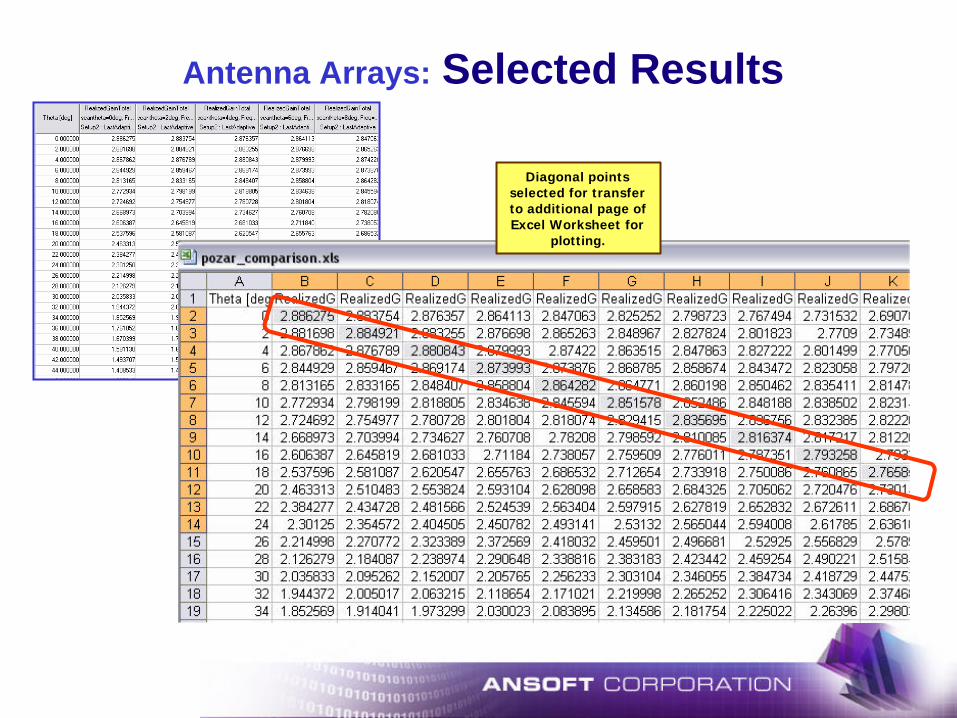
Antenna Arrays: Selected Results
Diagonal points selected for transfer to additional page of Excel Worksheet for
plotting.
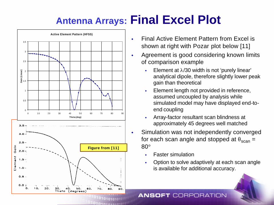
Antenna Arrays: Final Excel Plotw Final Active Element Pattern from Excel is
shown at right with Pozar plot below [11]w Agreement is good considering known limits
of comparison examplew Element at λ/30 width is not ‘purely linear’
analytical dipole, therefore slightly lower peak gain than theoretical
w Element length not provided in reference, assumed uncoupled by analysis while simulated model may have displayed end-to-end coupling
w Array-factor resultant scan blindness at approximately 45 degrees well matched
w Simulation was not independently converged for each scan angle and stopped at θscan = 80°w Faster simulationw Option to solve adaptively at each scan angle
is available for additional accuracy.
Active Element Pattern (HFSS)
0
0.5
1
1.5
2
2.5
3
3.5
0 1 0 2 0 30 40 5 0 60 70 80 90
Theta (deg)
Gai
n (L
inea
r)
Figure from [11]
Closing Remarks
w Frequency Selective Surfaces (FSS), Electromagnetic Bandgaps (EBGs), and Antenna Arrays all represent a periodic or latticed type radiation or scattering structure
w The same type of simulation techniques therefore apply to all such applications
w Today’s Wireless products are demanding more of their designs, such that lattice techniques for improving antenna performance may be of interest to both client-side and host/infrastructure level designers.w This morning’s Antenna Session, RB, contained three papers involving Antenna
Array applications and one involving EBGs. That’s four out of five in the session.
w Knowledge of modern simulation techniques for these applications is but an additional weapon in the designer’s arsenal
w We hope that this information may prove useful to you in the future, and thank you for your attention.

Acknowledgements
w The authors would also like to formally acknowledge the assistance of James Irion of Raytheon Corporation (McKinney, TX) for his suggestions regarding the extraction of the Active Element Pattern from HFSS™.
References[1] J. D. Kraus, Antennas – Second Edition, McGraw-Hill, 1988, ISBN 0070354227 [2] D.H. Schaubert, et al, “Moment method analysis of infinite stripline-fed tapered slot antenna
arrays with a ground plane,” IEEE Trans on Ant. and Prop. Vol. 42, Aug. 1994, pp. 1161-1166[3] Itoh, T., Pelosi, G. and Silvester, P. P., Finite Element Software for Microwave Engineering, J.
Wiley and Sons, New York, 1996, 484 pp. ISBN 0-471-12636-5 [4] Istvan Bardi and Zoltan Cendes, “New Directions in HFSS for Designing Microwave Devices,”
Microwave Journal, Vol 41, Number 8, August 1998, pp. 22-36[5] Ben A. Munk, Frequency Selective Surfaces: Theory and Design, John Wiley and Sons, New
York, 2000, ISBN 0-471-37047-9 [6] J. P. Berenger, “A Perfectly Matched Layer for the Absorption of Electromagnetic Waves,”
Journal of Computational Physics, No. 114, 1994, pp 185-200.[7] D. Sievenpiper, L. Zhang, R. F. J. Broas, N. G. Alexópolous, and E. Yablanovitch, “High-
Impedance Electromagnetic Surfaces with a Forbidden Frequency Band,” IEEE Transactions on Microwave Theory and Techniques, Vol 47, Number 11, November 1999, pp. 2059-2074.
[8] R. Remski, “Analysis of Photonic Bandgap Surfaces using Ansoft HFSS,” Microwave Journal, Volume 43, Number 9, September 2000.
[9] Cox, G.J.; Zorzos, K.; Seager, R.D.; Vardaxoglou, J.C., “Study of frequency selective surface (FSS) resonator elements on a circular dielectric rod antenna for mobile communications,”Antennas and Propagation, 2001. Eleventh International Conference on (IEE Conf. Publ. No. 480) , Volume: 2 , 2001, pp. 758 -761.
[10] I. Bardi, R. Remski, D. Perry and Z. Cendes, "Plane Wave Scattering from Frequency Selective Surfaces by the Finite Element Method", COMPUMAG Conference Proceedings, Evian France, July 2001
[11] D. M. Pozar, “The Active Element Pattern,” IEEE Transactions on Antennas and Propagation, Volume 42, No. 8, August 1994.