technology trends, wishes and dreams · 13.05.2012 · trends & wishes (various technologies...
TRANSCRIPT
Technology Trends, Wishes and Dreams
Detection and Imaging related

Reminder
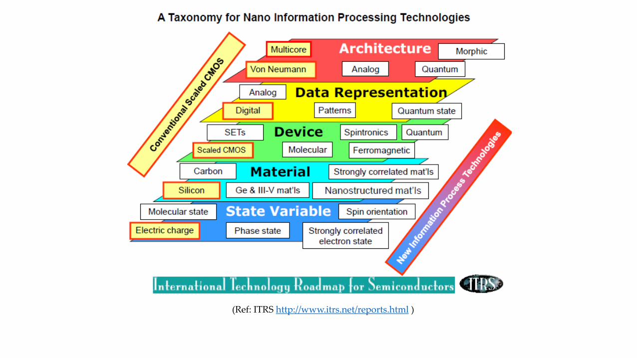
CMOS Scaling

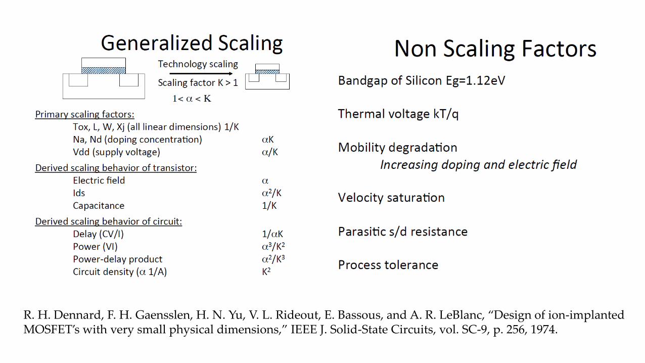
R. H. Dennard, F. H. Gaensslen, H. N. Yu, V. L. Rideout, E. Bassous, and A. R. LeBlanc, “Design of ion-implanted MOSFET’s with very small physical dimensions,” IEEE J. Solid-State Circuits, vol. SC-9, p. 256, 1974.
General Scaling Trends CMOS Transistors
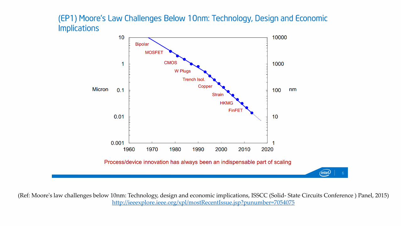
(Ref: Moore's law challenges below 10nm: Technology, design and economic implications, ISSCC (Solid- State Circuits Conference ) Panel, 2015)http://ieeexplore.ieee.org/xpl/mostRecentIssue.jsp?punumber=7054075
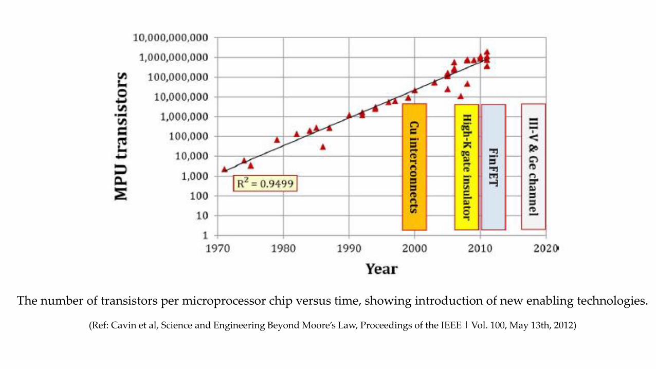
The number of transistors per microprocessor chip versus time, showing introduction of new enabling technologies.
(Ref: Cavin et al, Science and Engineering Beyond Moore’s Law, Proceedings of the IEEE | Vol. 100, May 13th, 2012)
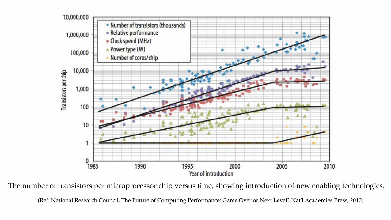
The number of transistors per microprocessor chip versus time, showing introduction of new enabling technologies.
(Ref: National Research Council, The Future of Computing Performance: Game Over or Next Level? Nat'l Academies Press, 2010)

Trends & Wishes(various technologies linked to detection and imaging)
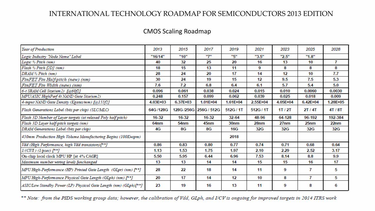
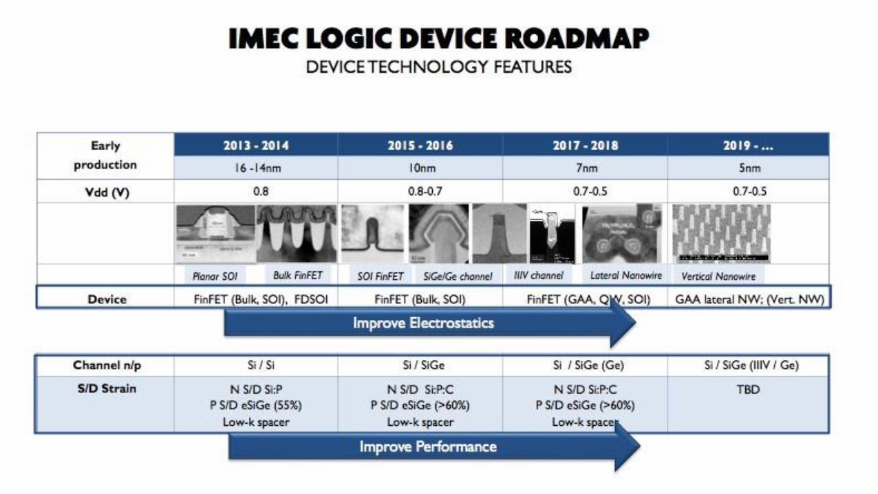
INTERNATIONAL TECHNOLOGY ROADMAP FOR SEMICONDUCTORS 2013 EDITION
CMOS Scaling Roadmap
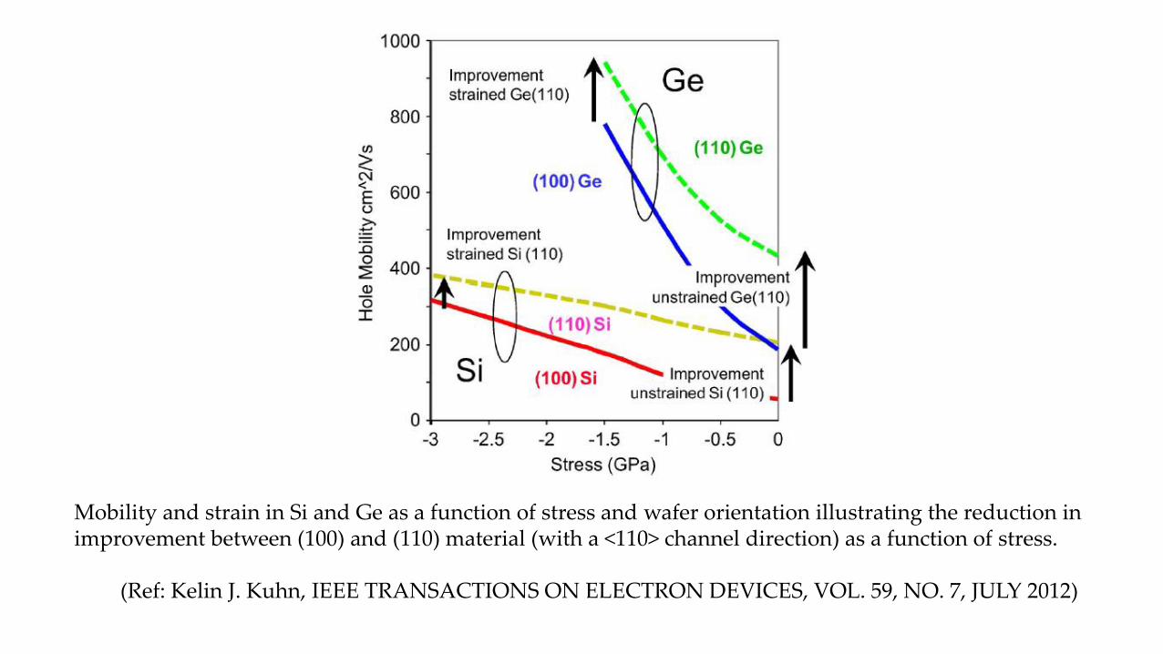
Mobility and strain in Si and Ge as a function of stress and wafer orientation illustrating the reduction in improvement between (100) and (110) material (with a <110> channel direction) as a function of stress.
(Ref: Kelin J. Kuhn, IEEE TRANSACTIONS ON ELECTRON DEVICES, VOL. 59, NO. 7, JULY 2012)
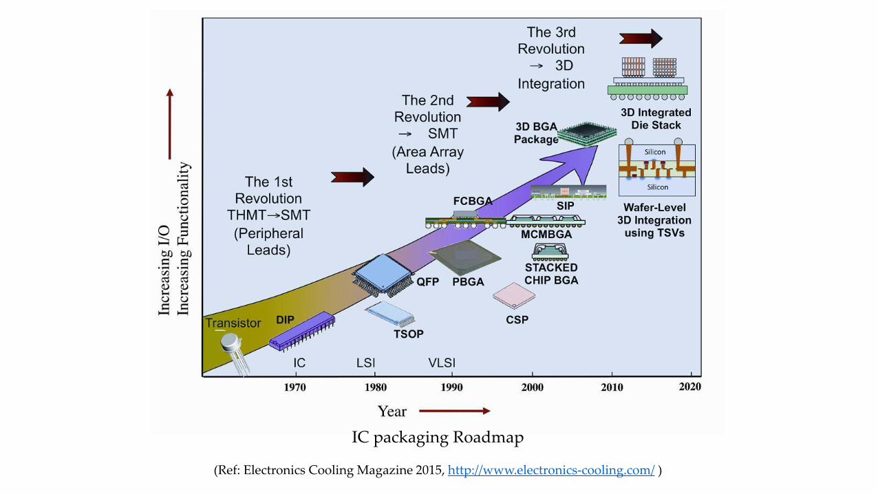
IC packaging Roadmap
(Ref: Electronics Cooling Magazine 2015, http://www.electronics-cooling.com/ )
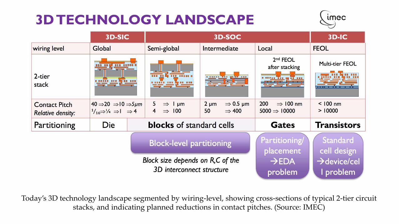
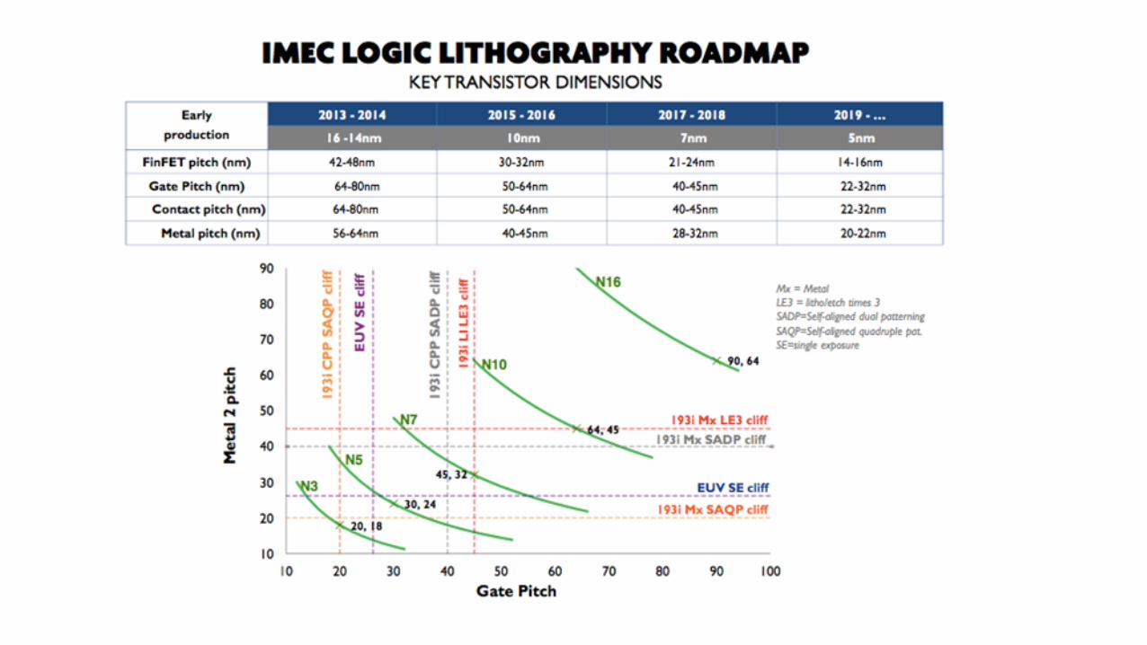
Today’s 3D technology landscape segmented by wiring-level, showing cross-sections of typical 2-tier circuit stacks, and indicating planned reductions in contact pitches. (Source: IMEC)
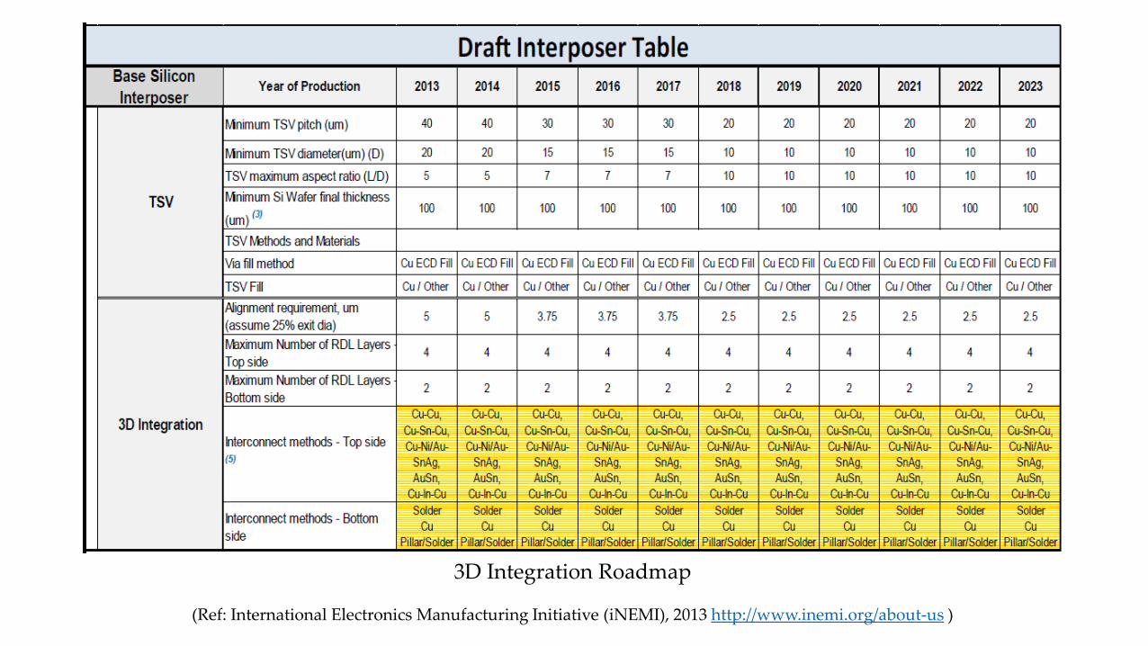
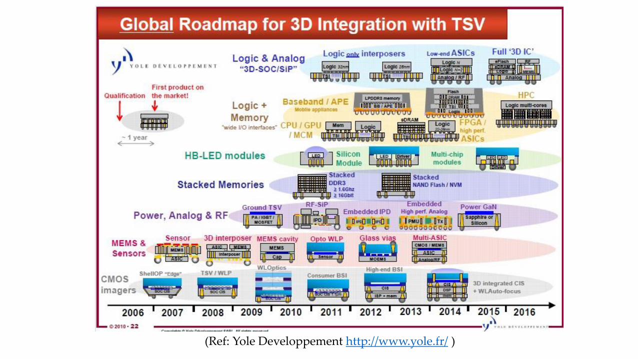
3D Integration Roadmap
(Ref: International Electronics Manufacturing Initiative (iNEMI), 2013 http://www.inemi.org/about-us )
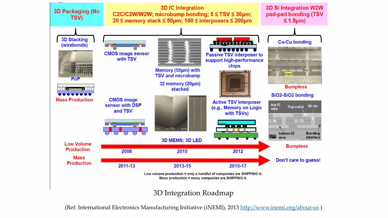
3D Integration Roadmap
(Ref: International Electronics Manufacturing Initiative (iNEMI), 2013 http://www.inemi.org/about-us )
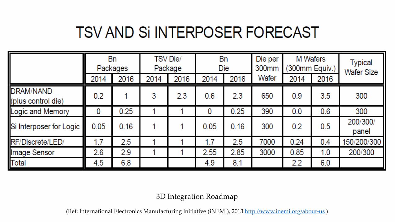
3D Integration Roadmap
(Ref: International Electronics Manufacturing Initiative (iNEMI), 2013 http://www.inemi.org/about-us )
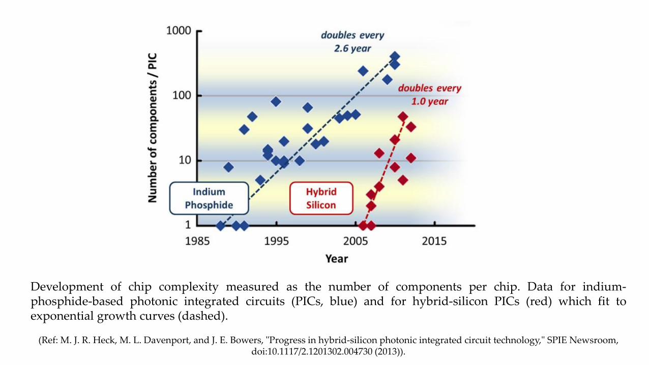
Development of chip complexity measured as the number of components per chip. Data for indium-phosphide-based photonic integrated circuits (PICs, blue) and for hybrid-silicon PICs (red) which fit toexponential growth curves (dashed).
(Ref: M. J. R. Heck, M. L. Davenport, and J. E. Bowers, "Progress in hybrid-silicon photonic integrated circuit technology," SPIE Newsroom, doi:10.1117/2.1201302.004730 (2013)).
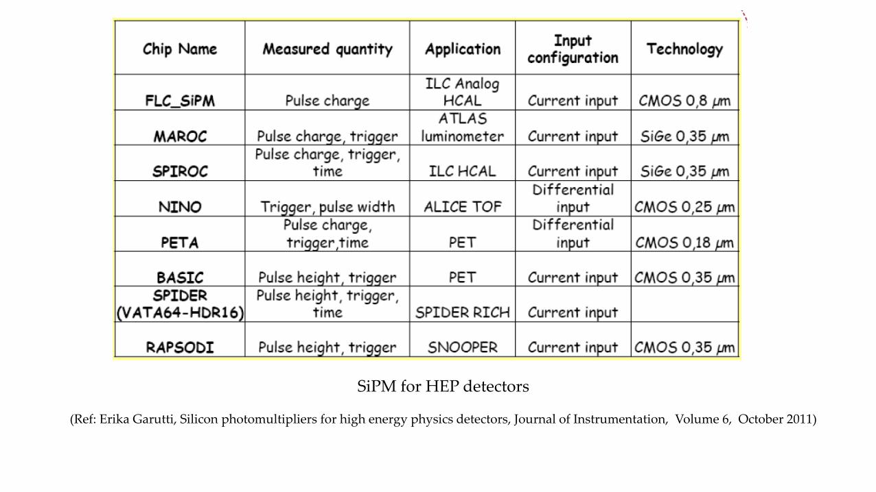
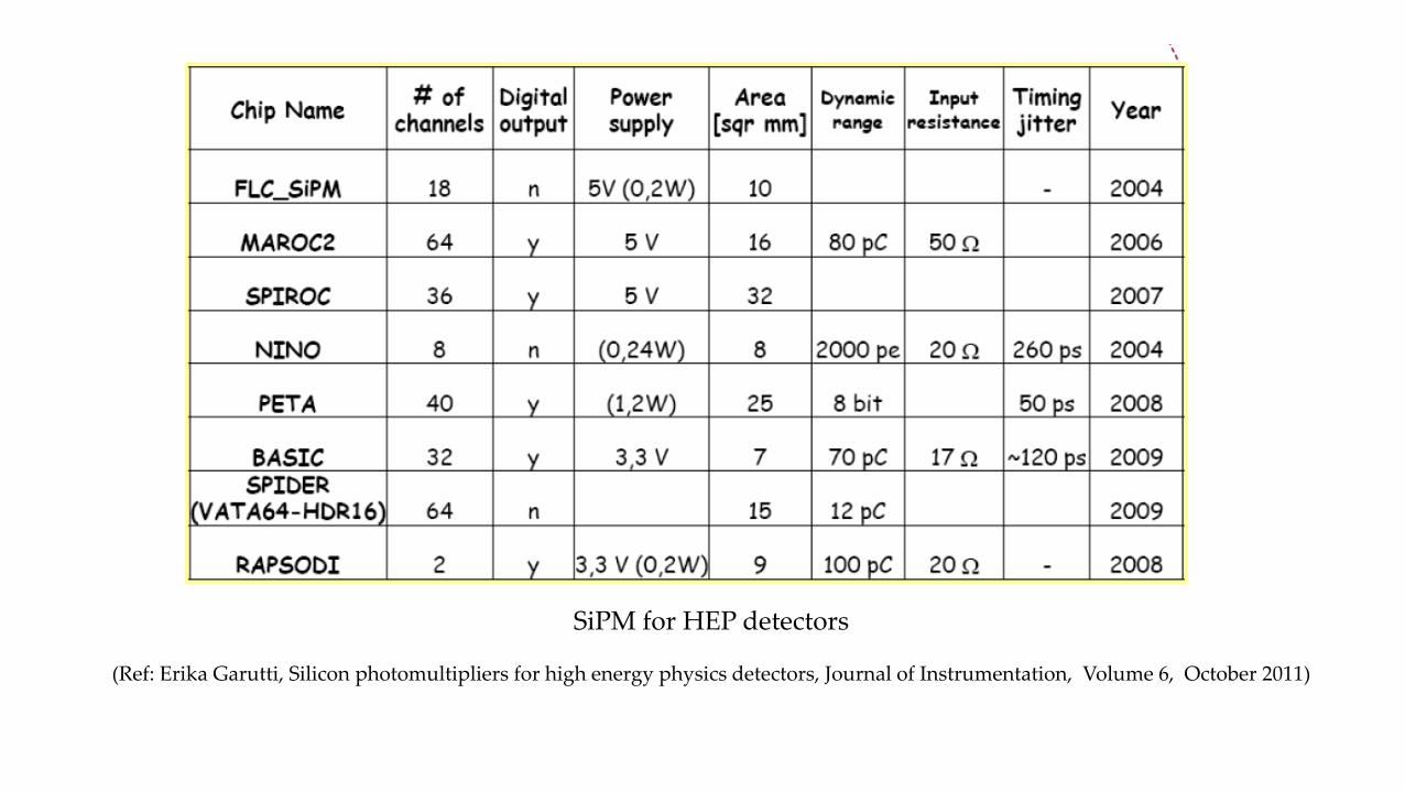
SiPM for HEP detectors
(Ref: Erika Garutti, Silicon photomultipliers for high energy physics detectors, Journal of Instrumentation, Volume 6, October 2011)
SiPM for HEP detectors
(Ref: Erika Garutti, Silicon photomultipliers for high energy physics detectors, Journal of Instrumentation, Volume 6, October 2011)
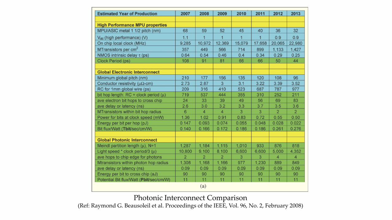
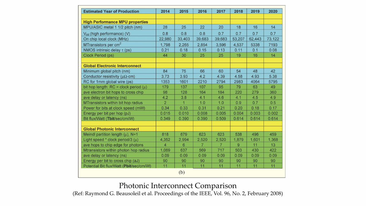
Photonic Interconnect Comparison (Ref: Raymond G. Beausoleil et al. Proceedings of the IEEE, Vol. 96, No. 2, February 2008)
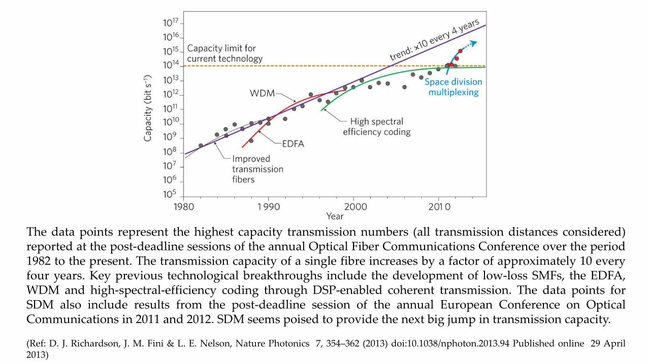
The data points represent the highest capacity transmission numbers (all transmission distances considered)reported at the post-deadline sessions of the annual Optical Fiber Communications Conference over the period1982 to the present. The transmission capacity of a single fibre increases by a factor of approximately 10 everyfour years. Key previous technological breakthroughs include the development of low-loss SMFs, the EDFA,WDM and high-spectral-efficiency coding through DSP-enabled coherent transmission. The data points forSDM also include results from the post-deadline session of the annual European Conference on OpticalCommunications in 2011 and 2012. SDM seems poised to provide the next big jump in transmission capacity.
(Ref: D. J. Richardson, J. M. Fini & L. E. Nelson, Nature Photonics 7, 354–362 (2013) doi:10.1038/nphoton.2013.94 Published online 29 April2013)
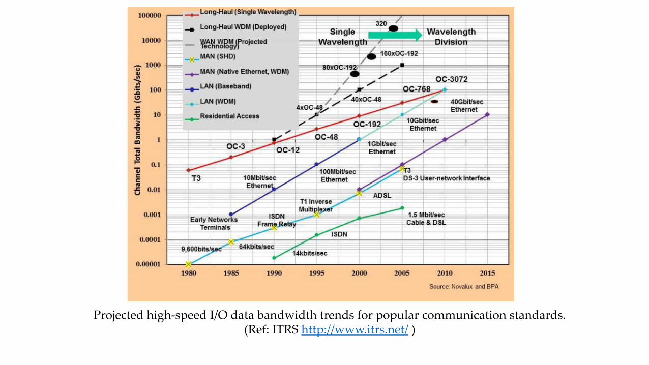
Projected high-speed I/O data bandwidth trends for popular communication standards. (Ref: ITRS http://www.itrs.net/ )
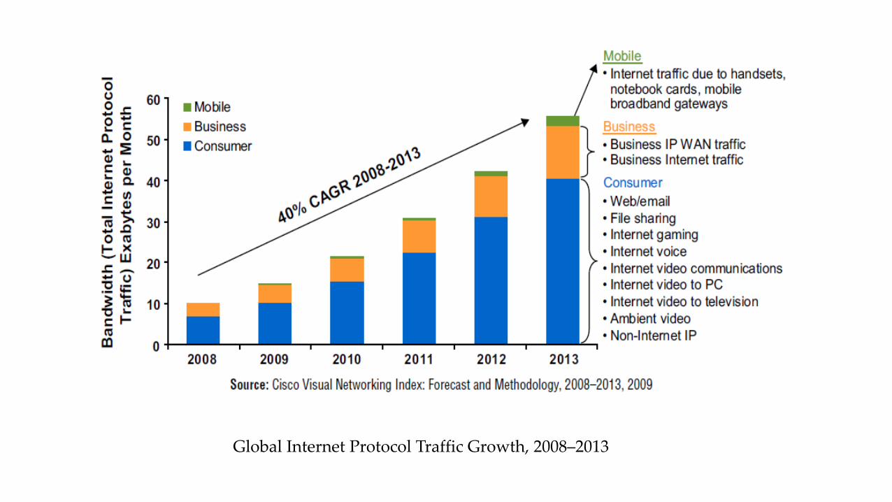
Global Internet Protocol Traffic Growth, 2008–2013
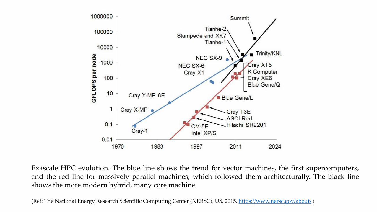
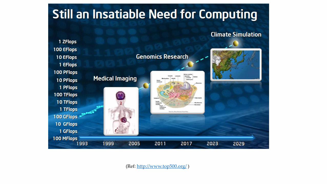
Exascale HPC evolution. The blue line shows the trend for vector machines, the first supercomputers,and the red line for massively parallel machines, which followed them architecturally. The black lineshows the more modern hybrid, many core machine.
(Ref: The National Energy Research Scientific Computing Center (NERSC), US, 2015, https://www.nersc.gov/about/ )

Dreams(various technologies)
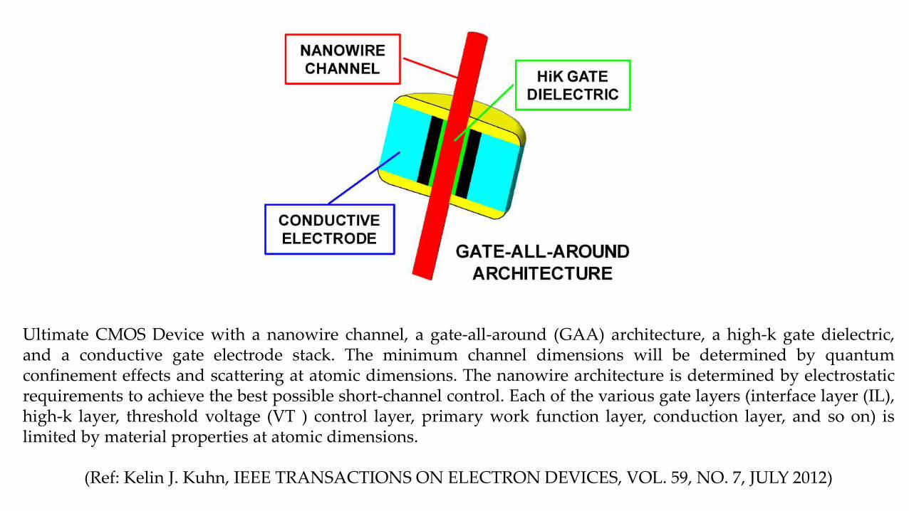
Ultimate CMOS Device with a nanowire channel, a gate-all-around (GAA) architecture, a high-k gate dielectric,and a conductive gate electrode stack. The minimum channel dimensions will be determined by quantumconfinement effects and scattering at atomic dimensions. The nanowire architecture is determined by electrostaticrequirements to achieve the best possible short-channel control. Each of the various gate layers (interface layer (IL),high-k layer, threshold voltage (VT ) control layer, primary work function layer, conduction layer, and so on) islimited by material properties at atomic dimensions.
(Ref: Kelin J. Kuhn, IEEE TRANSACTIONS ON ELECTRON DEVICES, VOL. 59, NO. 7, JULY 2012)
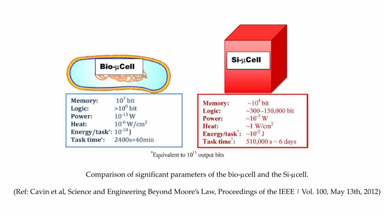
Comparison of significant parameters of the bio-cell and the Si-cell.
(Ref: Cavin et al, Science and Engineering Beyond Moore’s Law, Proceedings of the IEEE | Vol. 100, May 13th, 2012)
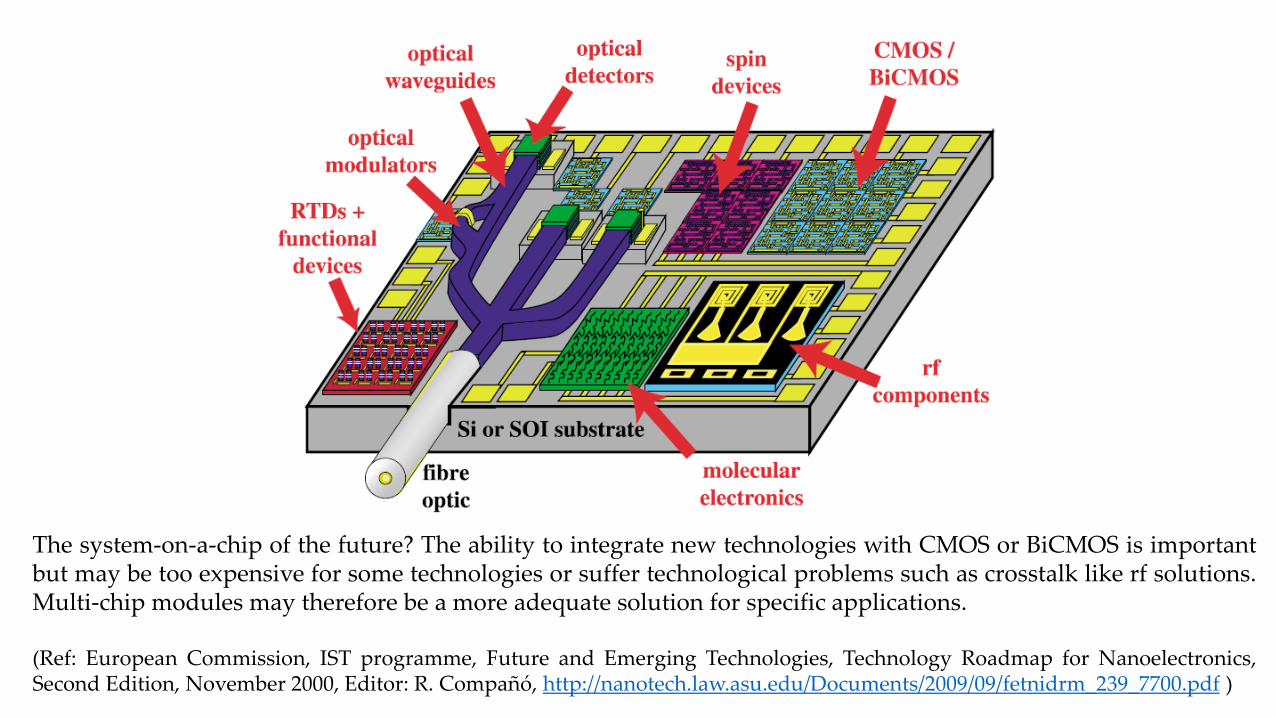
The system-on-a-chip of the future? The ability to integrate new technologies with CMOS or BiCMOS is importantbut may be too expensive for some technologies or suffer technological problems such as crosstalk like rf solutions.Multi-chip modules may therefore be a more adequate solution for specific applications.
(Ref: European Commission, IST programme, Future and Emerging Technologies, Technology Roadmap for Nanoelectronics,Second Edition, November 2000, Editor: R. Compañó, http://nanotech.law.asu.edu/Documents/2009/09/fetnidrm_239_7700.pdf )
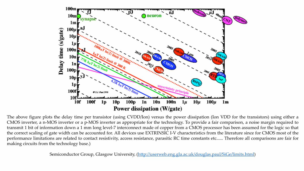
The above figure plots the delay time per transistor (using CVDD/Ion) versus the power dissipation (Ion VDD for the transistors) using either aCMOS inverter, a n-MOS inverter or a p-MOS inverter as appropriate for the technology. To provide a fair comparison, a noise margin required totransmit 1 bit of information down a 1 mm long level-7 interconnect made of copper from a CMOS processor has been assumed for the logic so thatthe correct scaling of gate width can be accounted for. All devices use EXTRINSIC I-V characteristics from the literature since for CMOS most of theperformance limitations are related to contact resistivity, access resistance, parasitic RC time constants etc...... Therefore all comparisons are fair formaking circuits from the technology base.)
Semiconductor Group, Glasgow University, (http://userweb.eng.gla.ac.uk/douglas.paul/SiGe/limits.html)
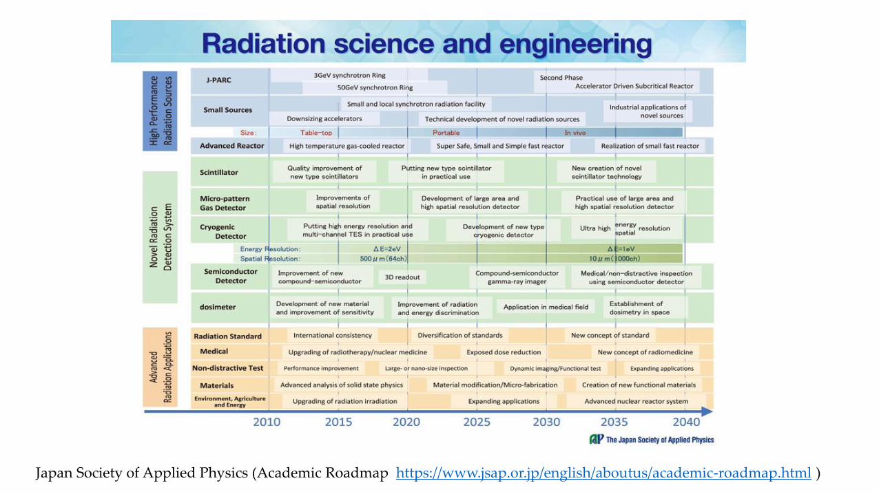
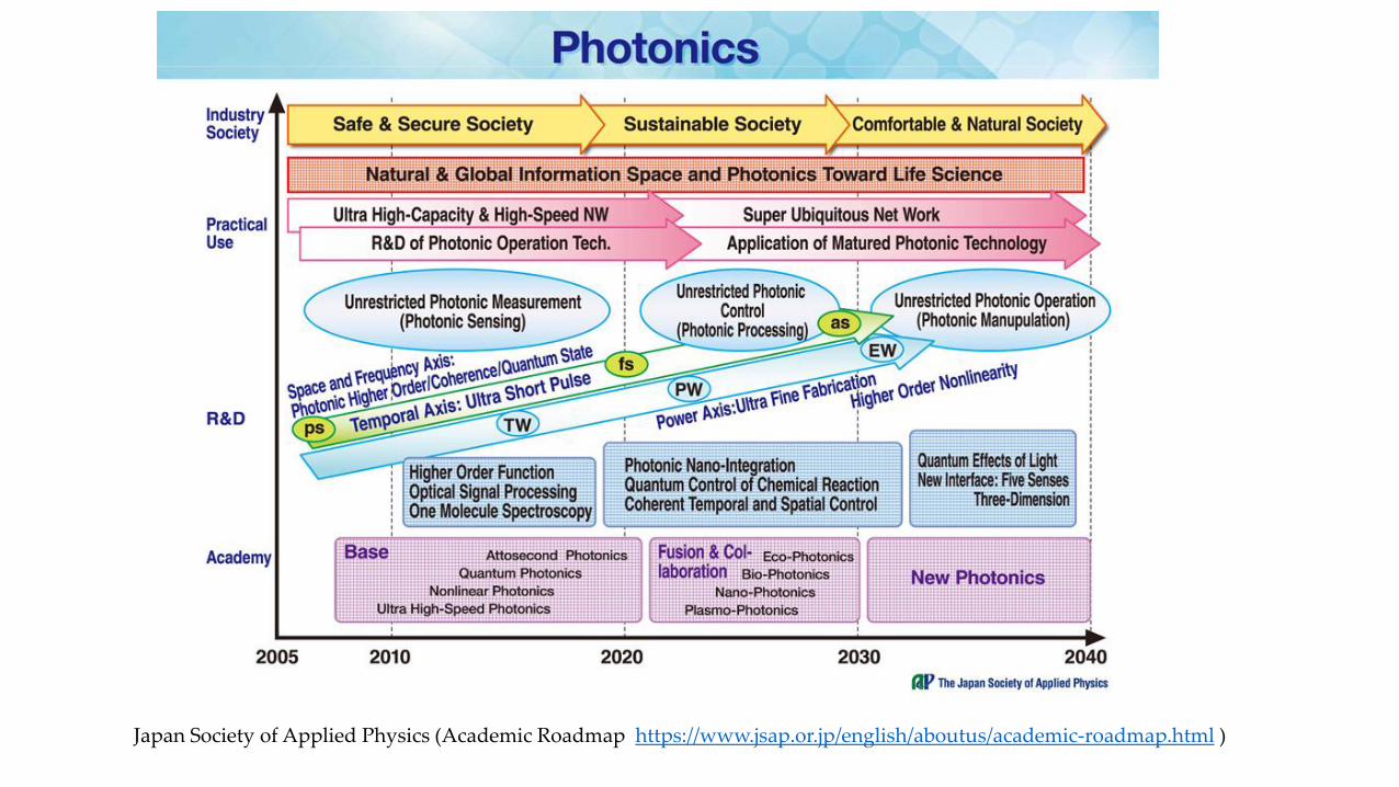
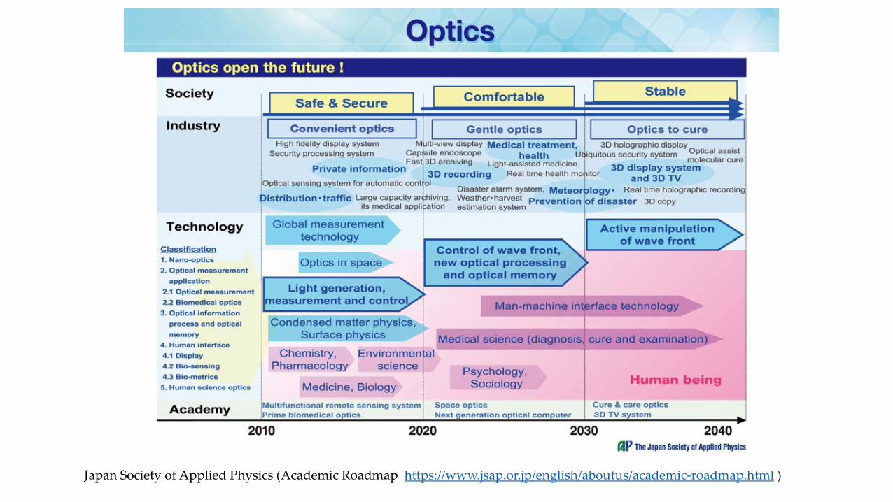
Japan Society of Applied Physics (Academic Roadmap https://www.jsap.or.jp/english/aboutus/academic-roadmap.html )
Japan Society of Applied Physics (Academic Roadmap https://www.jsap.or.jp/english/aboutus/academic-roadmap.html )
Photonic Interconnect Comparison (Ref: Raymond G. Beausoleil et al. Proceedings of the IEEE, Vol. 96, No. 2, February 2008)
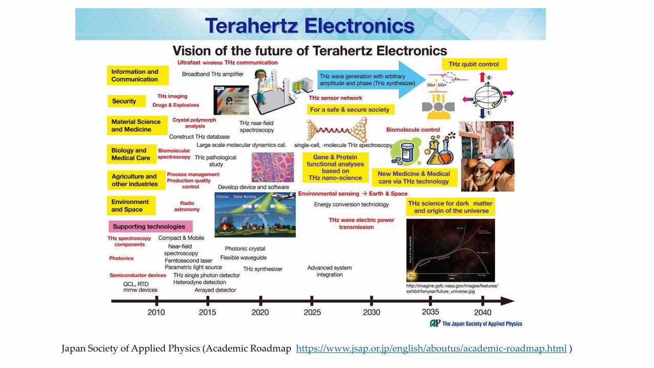
Japan Society of Applied Physics (Academic Roadmap https://www.jsap.or.jp/english/aboutus/academic-roadmap.html )

Japan Society of Applied Physics (Academic Roadmap https://www.jsap.or.jp/english/aboutus/academic-roadmap.html )
Japan Society of Applied Physics (Academic Roadmap https://www.jsap.or.jp/english/aboutus/academic-roadmap.html )
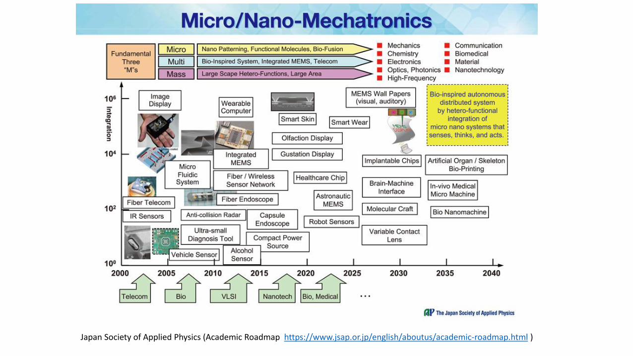
Japan Society of Applied Physics (Academic Roadmap https://www.jsap.or.jp/english/aboutus/academic-roadmap.html )
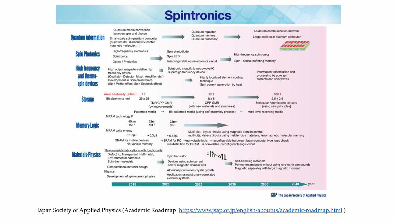
Japan Society of Applied Physics (Academic Roadmap https://www.jsap.or.jp/english/aboutus/academic-roadmap.html )
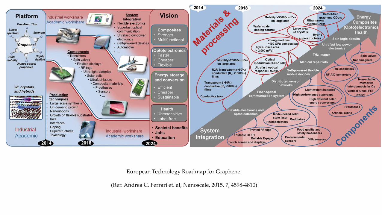
European Technology Roadmap for Graphene
(Ref: Andrea C. Ferrari et. al, Nanoscale, 2015, 7, 4598-4810)
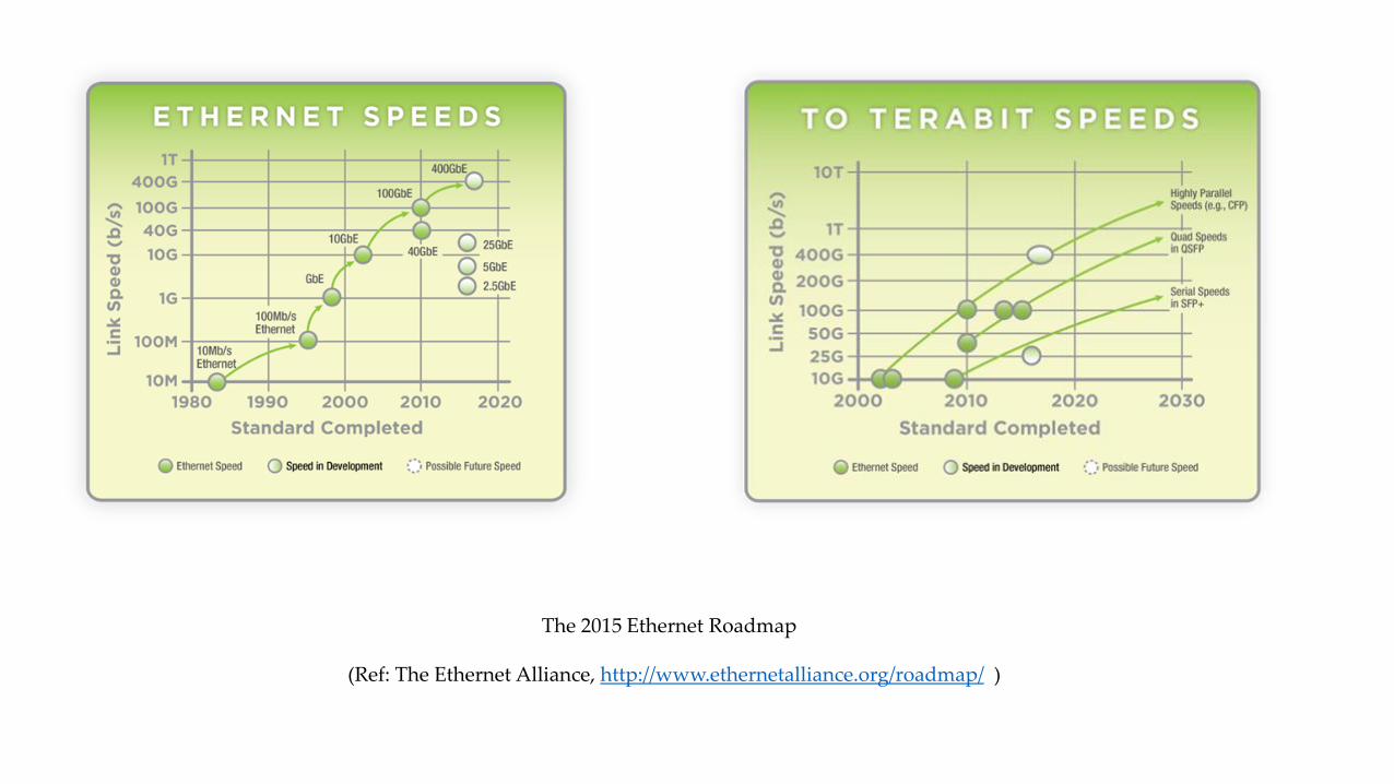
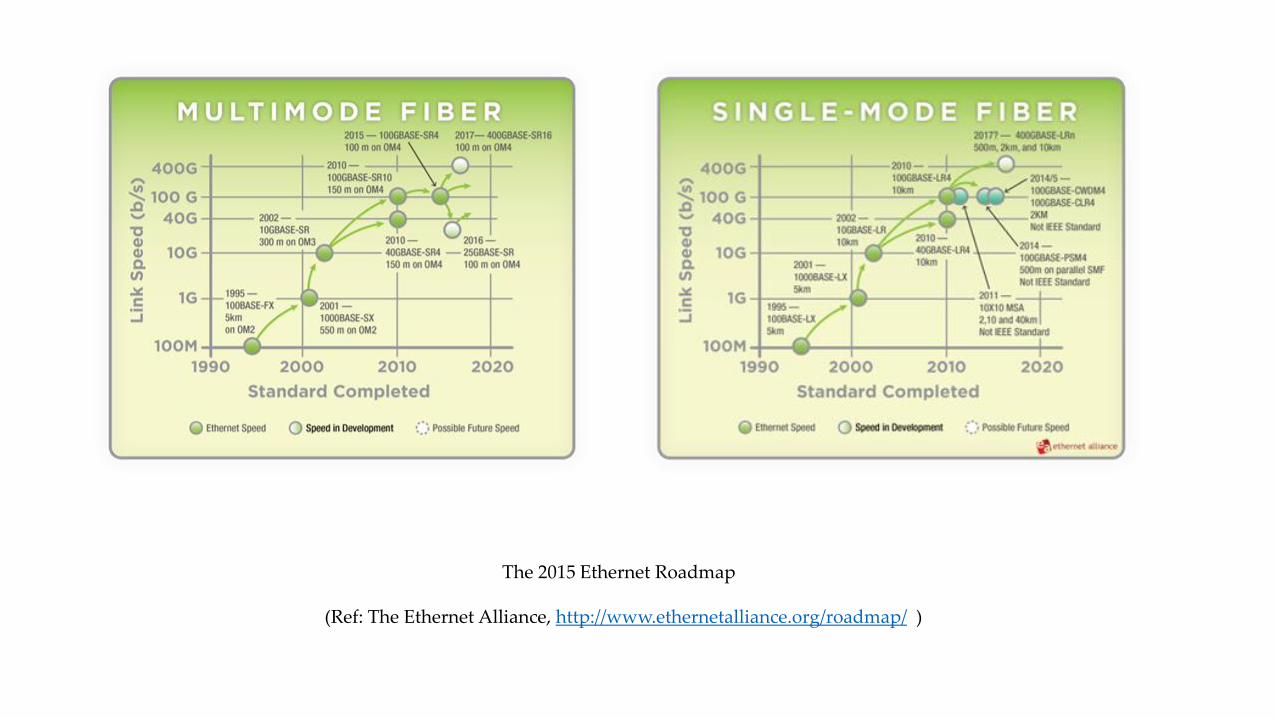
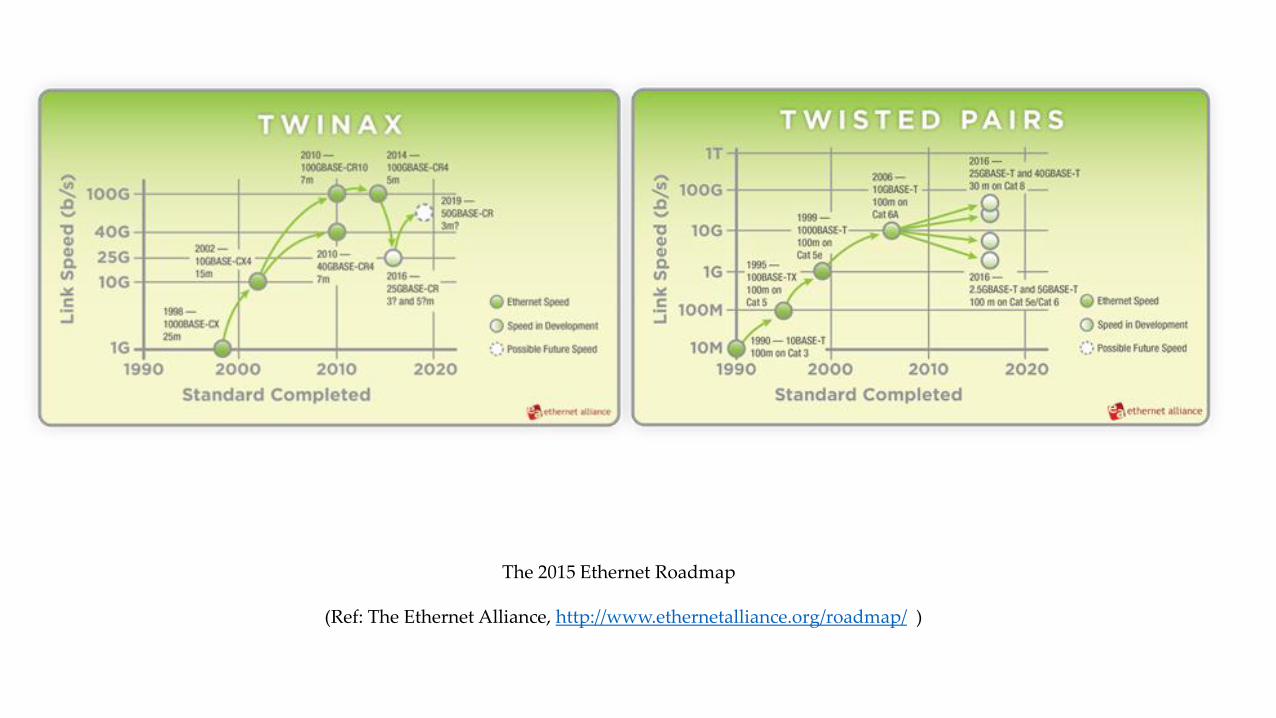
The 2015 Ethernet Roadmap
(Ref: The Ethernet Alliance, http://www.ethernetalliance.org/roadmap/ )
The 2015 Ethernet Roadmap
(Ref: The Ethernet Alliance, http://www.ethernetalliance.org/roadmap/ )
The 2015 Ethernet Roadmap
(Ref: The Ethernet Alliance, http://www.ethernetalliance.org/roadmap/ )
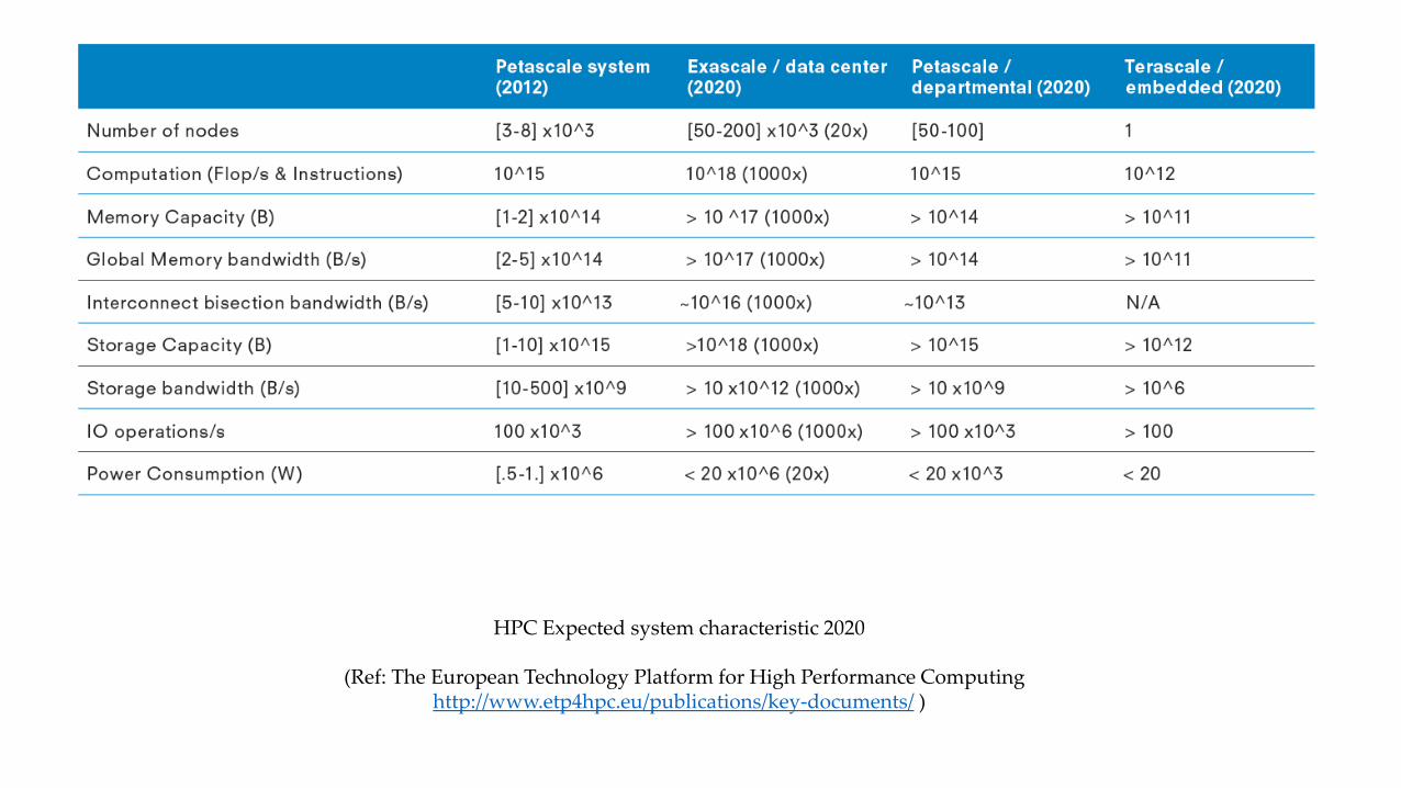
HPC Expected system characteristic 2020
(Ref: The European Technology Platform for High Performance Computing http://www.etp4hpc.eu/publications/key-documents/ )
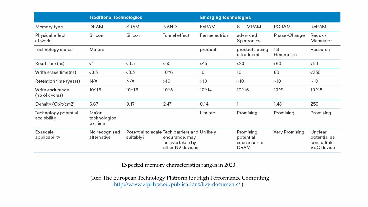
Expected memory characteristics ranges in 2020
(Ref: The European Technology Platform for High Performance Computing http://www.etp4hpc.eu/publications/key-documents/ )
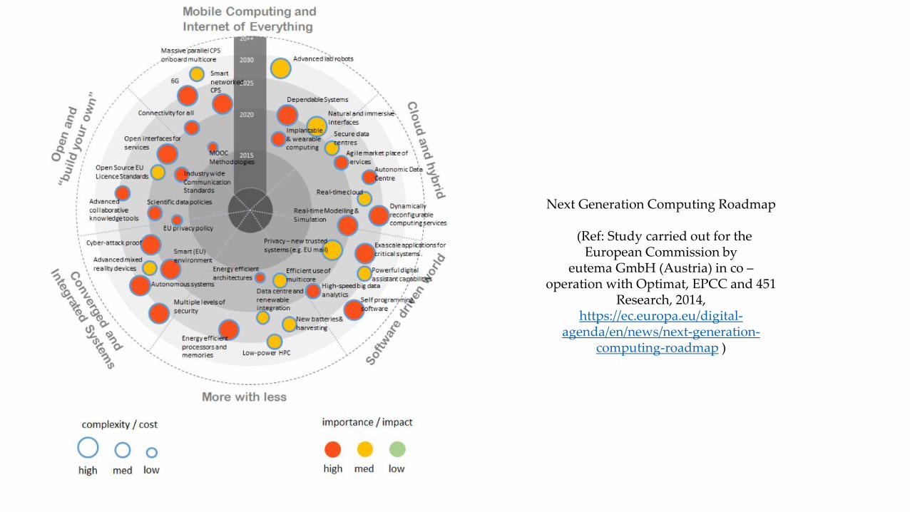
Next Generation Computing Roadmap
(Ref: Study carried out for the European Commission by
eutema GmbH (Austria) in co –operation with Optimat, EPCC and 451
Research, 2014, https://ec.europa.eu/digital-
agenda/en/news/next-generation-computing-roadmap )
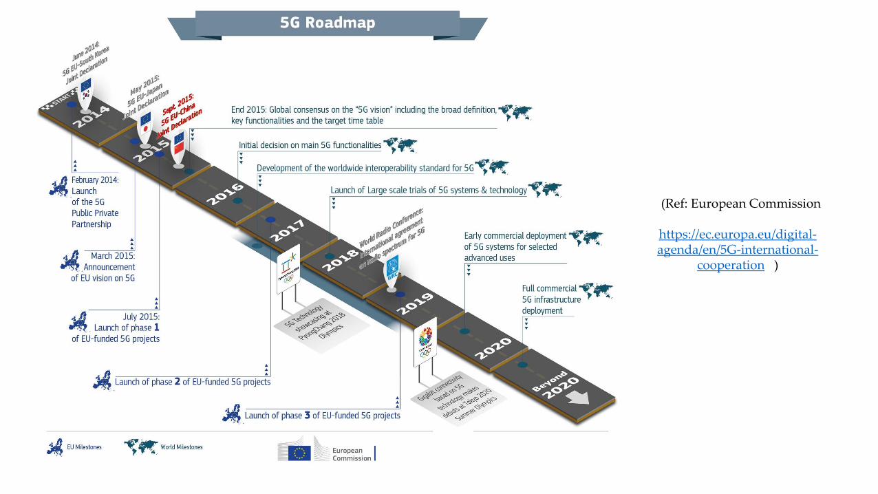
(Ref: European Commission
https://ec.europa.eu/digital-agenda/en/5G-international-
cooperation )