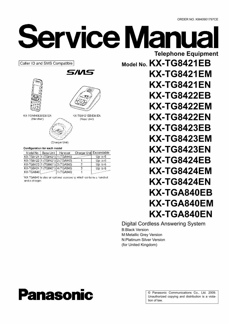
telephone equipment model no. kx-tg8421eb kx … equipment model no. kx-tg8421eb kx-tg8421em...
TRANSCRIPT
© Panasonic Communications Co., Ltd. 2009.Unauthorized copying and distribution is a viola-tion of law.
ORDER NO. KM40901797CE
Telephone EquipmentModel No. KX-TG8421EB
KX-TG8421EMKX-TG8421ENKX-TG8422EBKX-TG8422EMKX-TG8422ENKX-TG8423EBKX-TG8423EMKX-TG8423ENKX-TG8424EBKX-TG8424EMKX-TG8424ENKX-TGA840EBKX-TGA840EMKX-TGA840EN
Digital Cordless Answering SystemB:Black VersionM:Metallic Grey VersionN:Platinum Silver Version(for United Kingdom)
2
KX-TG8421E/KX-TG8422E/KX-TG8423E/KX-TG8424E/KX-TGA840E

3
KX-TG8421E/KX-TG8422E/KX-TG8423E/KX-TG8424E/KX-TGA840E
TABLE OF CONTENTSPAGE PAGE
1 Safety Precautions----------------------------------------------- 41.1. For Service Technicians --------------------------------- 4
2 Warning -------------------------------------------------------------- 42.1. Battery Caution--------------------------------------------- 42.2. About Lead Free Solder (Pbf: Pb free)--------------- 42.3. Discarding of P.C. Board--------------------------------- 5
3 Specifications ----------------------------------------------------- 64 Technical Descriptions ----------------------------------------- 7
4.1. Block Diagram (Base Unit) ------------------------------ 74.2. Circuit Operation (Base Unit) --------------------------- 84.3. Block Diagram (Handset)-------------------------------114.4. Circuit Operation (Handset)----------------------------124.5. Circuit Operation (Charger Unit) ----------------------134.6. Signal Route -----------------------------------------------14
5 Location of Controls and Components ------------------165.1. Controls -----------------------------------------------------16
6 Setting up ----------------------------------------------------------176.1. Connections------------------------------------------------176.2. Battery-------------------------------------------------------17
7 Operating Instructions-----------------------------------------197.1. Programmable Settings---------------------------------197.2. Registering a Handset to a Base Unit ---------------227.3. Copying Phonebook Entries ---------------------------237.4. Error Messages -------------------------------------------237.5. Troubleshooting-------------------------------------------247.6. For Service Hint-------------------------------------------28
8 Service Mode -----------------------------------------------------298.1. Engineering Mode----------------------------------------298.2. Copying Phonebook Items when Repairing -------338.3. How to Clear User Setting------------------------------35
9 Troubleshooting Guide ----------------------------------------369.1. Troubleshooting Flowchart -----------------------------369.2. Troubleshooting by Symptom (Base Unit and
Charger Unit) ----------------------------------------------489.3. Troubleshooting by Symptom (Handset) -----------52
10 Disassembly and Assembly Instructions ---------------5610.1. Disassembly Instructions -------------------------------5610.2. How to Replace the Handset LCD -------------------60
11 Measurements and Adjustments---------------------------6111.1. The Setting Method of JIG (Base Unit) -------------6111.2. Adjustment Standard (Base Unit)---------------------6311.3. Adjustment Standard (Charger Unit)-----------------6411.4. The Setting Method of JIG (Handset) ---------------6511.5. Adjustment Standard (Handset) ----------------------6711.6. Things to Do after Replacing IC or X'tal ------------6811.7. RF Specification-------------------------------------------7011.8. How to Check the Handset Speaker or
Receiver ----------------------------------------------------7111.9. Frequency Table (MHz) ---------------------------------71
12 Miscellaneous ----------------------------------------------------7212.1. CPU Data (Base Unit) -----------------------------------7212.2. CPU Data (Handset)-------------------------------------7412.3. How to Replace the Flat Package IC----------------7612.4. How to Replace the LLP (Leadless Leadframe
Package) IC------------------------------------------------7812.5. Terminal Guide of the ICs, Transistors and
Diodes -------------------------------------------------------8013 Schematic Diagram ---------------------------------------------82
13.1. For Schematic Diagram -------------------------------- 8213.2. Schematic Diagram (Base Unit)---------------------- 8413.3. Schematic Diagram (Base Unit_Operation) ------- 8613.4. Schematic Diagram (Handset)------------------------ 8813.5. Schematic Diagram (Charger Unit)------------------ 90
14 Printed Circuit Board ------------------------------------------ 9114.1. Circuit Board (Base Unit_MAIN) --------------------- 9114.2. Circuit Board (Base Unit_Operation)---------------- 9314.3. Circuit Board (Handset) -------------------------------- 9414.4. Circuit Board (Charger Unit)--------------------------- 96
15 Exploded View and Replacement Parts List ----------- 9715.1. Cabinet and Electrical Parts (Base Unit) ----------- 9715.2. Cabinet and Electrical Parts (Handset)------------- 9815.3. Cabinet and Electrical Parts (Charger Unit) ------- 9915.4. Accessories and Packing Materials --------------- 10015.5. Replacement Part List -------------------------------- 105
4
KX-TG8421E/KX-TG8422E/KX-TG8423E/KX-TG8424E/KX-TGA840E
1 Safety Precautions1.1. For Service Technicians
• Repair service shall be provided in accordance with repair technology information such as service manual so as to pre-vent fires, injury or electric shock, which can be caused by improper repair work.1. When repair services are provided, neither the products nor their parts or members shall be remodeled. 2. If a lead wire assembly is supplied as a repair part, the lead wire assembly shall be replaced.3. FASTON terminals shall be plugged straight in and unplugged straight out.
• ICs and LSIs are vulnerable to static electricity.When repairing, the following precautions will help prevent recurring malfunctions.1. Cover plastic parts boxes with aluminum foil.2. Ground the soldering irons.3. Use a conductive mat on worktable.4. Do not grasp IC or LSI pins with bare fingers.
2 Warning2.1. Battery Caution
1. Danger of explosion if battery is incorrectly replaced.2. Replace only with the same or equivalent type recommended by the manufacturer.3. Dispose of used batteries according to the manufacture’s Instructions.
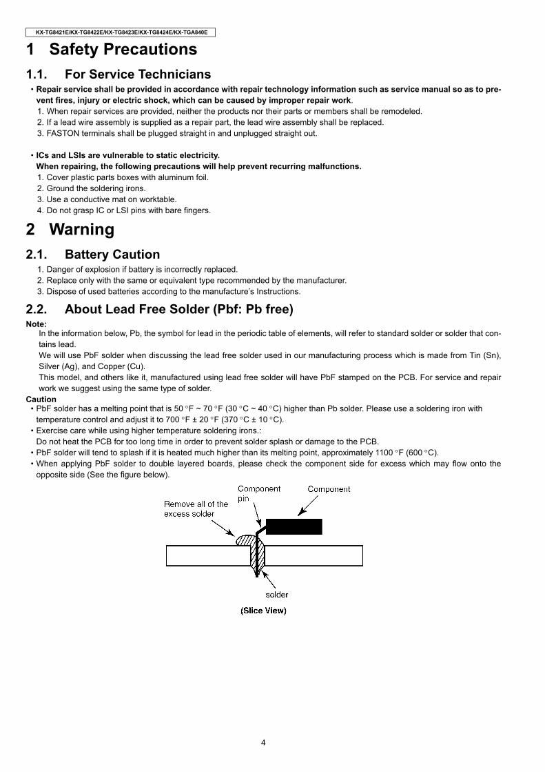
2.2. About Lead Free Solder (Pbf: Pb free)Note:
In the information below, Pb, the symbol for lead in the periodic table of elements, will refer to standard solder or solder that con-tains lead.We will use PbF solder when discussing the lead free solder used in our manufacturing process which is made from Tin (Sn),Silver (Ag), and Copper (Cu).This model, and others like it, manufactured using lead free solder will have PbF stamped on the PCB. For service and repairwork we suggest using the same type of solder.
Caution• PbF solder has a melting point that is 50 °F ~ 70 °F (30 °C ~ 40 °C) higher than Pb solder. Please use a soldering iron with
temperature control and adjust it to 700 °F ± 20 °F (370 °C ± 10 °C). • Exercise care while using higher temperature soldering irons.:
Do not heat the PCB for too long time in order to prevent solder splash or damage to the PCB.• PbF solder will tend to splash if it is heated much higher than its melting point, approximately 1100 °F (600 °C).• When applying PbF solder to double layered boards, please check the component side for excess which may flow onto the
opposite side (See the figure below).

5
KX-TG8421E/KX-TG8422E/KX-TG8423E/KX-TG8424E/KX-TGA840E
2.2.1. Suggested PbF SolderThere are several types of PbF solder available commercially. While this product is manufactured using Tin, Silver, and Copper(Sn+Ag+Cu), you can also use Tin and Copper (Sn+Cu) or Tin, Zinc, and Bismuth (Sn+Zn+Bi). Please check the manufacturer’sspecific instructions for the melting points of their products and any precautions for using their product with other materials. The following lead free (PbF) solder wire sizes are recommended for service of this product: 0.3 mm, 0.6 mm and 1.0 mm.
2.3. Discarding of P.C. BoardWhen discarding P. C. Board, delete all personal information such as telephone directory and caller list or scrap P. C. Board.

6
KX-TG8421E/KX-TG8422E/KX-TG8423E/KX-TG8424E/KX-TGA840E
3 Specifications
Note:• Design and specifications are subject to change without notice.
Note for Service:• Operation range: Up to 300 m outdoors, Up to 50 m indoors, depending on the condition.• Analog telephone connection: Telephone Line• Optional headset: KX-TCA94EX

7
KX-TG8421E/KX-TG8422E/KX-TG8423E/KX-TG8424E/KX-TGA840E
4 Technical Descriptions4.1. Block Diagram (Base Unit)
Ana
log
Fro
ntE
nd
To
TE
L_LI
NE
Brid
geR
ect D
3D
3H
ook
Sw
itch
Q4,
Q5
Aud
io
Bel
l/Cal
ler
IDIn
terf
ace
CP
U
18 16 23 20 21 19 24B
ELL
HO
OK
Off-
Hoo
k Li
ne V
olta
ge25
A/D
D/A
AD
PC
MC
odec
Filt
er
DS
P
Spe
ech
Enc
odin
g
Spe
ech
Dec
odin
g
BM
C
Bur
st E
ncod
ing
Bur
st D
ecod
ing
RF
PLL
5 3 7775 9 10
EE
PR
OM
SC
L
SD
A
57 58 44
To
AC
Ada
ptor
Lim
itR
esis
tor
Cha
rge
Det
ecto
r
CH
AR
GE
CO
NT
AC
T
(Opt
iona
l)
VU
NR
EG
3.0V
Reg
.IC
1
2.4V
Reg
.Q
9
1.8V
Reg
.Q
83.0
V
2.4
V
1.8
V
BB
ICIC
401
IC7 K
X-T
G84
21/8
422/
8423
/842
4 B
LOC
K D
IAG
RA
M (
BA
SE
UN
IT)
MO
D/D
EM
OD
Cha
rge
Pum
p
43
2.5V
XT
AL
X1
X1
10.3
68M
Hz
IC80
1
RX
n
RX
p
TX
p
TX
n
Pon
PS
EL
VD
D-P
AD
RV
4 3 6 7
TX
on
RX
on
D80
1
6 72
AN
T1
AN
T2
9 8
AN
T1
AN
T2
RF
PA
AN
T1
AN
T2
78 73 74 80
L1 L2
L1 L2
2
FLA
SH
ME
MO
RY
IC42
1
42
3.0V
5455
5653 TAM-CSN
SPI-DISPI-DO
SPICLK

8
KX-TG8421E/KX-TG8422E/KX-TG8423E/KX-TG8424E/KX-TGA840E
4.2. Circuit Operation (Base Unit)4.2.1. Outline
Base Unit consists of the following ICs as shown in Block Diagram (Base Unit) (P.7).• DECT BBIC (Base Band IC): IC7
- Handling all the audio, signal and data processing needed in a DECT base unit- Controlling the DECT specific physical layer and radio section (Burst Module Controller section)- ADPCM code filter for speech encoding and speech decoding (DSP section)- Echo-cancellation and Echo-suppression (DSP section)- Any tones (tone, sidetone, ringing tone, etc.) generation (DSP section)- DTMF receiver (DSP section)- Clock Generation for RF Module- ADC, DAC, timer, and power control circuitry- PLL Oscillator- Detector - Compress/Expander- First Mixer- All interfaces (ex: RF Power Amp, EEPROM, LED, Analog Front End, etc.)
• RF Power Amp.: IC801- Amplifier for transmission and reception
• EEPROM: IC401- Temporary operating parameters (for RF, etc.)
• FLASH MEMORY: IC421- Voice Prompt (TAM) D/L Area- ICM/OGM Recording Area
• Additionally,- Power Supply Circuit (+3.0 V, +2.4 V, +1.8 V output)- Crystal Circuit (10.368 MHz)- Charge Circuit- Telephone Line Interface Circuit

9
KX-TG8421E/KX-TG8422E/KX-TG8423E/KX-TG8424E/KX-TGA840E
4.2.2. Power Supply CircuitThe power is supplied to the DECT BBIC, RF Module, EEPROM and Charge Contact from AC Adaptor (+6.5 V) as shown inFig.101. The power supply is as follows;
• DECT BBIC (IC7): DC Jack (+6.5 V) →D1→ IC1 → IC7DC Jack (+6.5 V) →D1→ IC1 → Q9 → IC7DC Jack (+6.5 V) →D1→ IC1 → Q8 → IC7
• RF Power Amp. (IC801): DC Jack (+6.5 V) →D1→ IC1 → IC801 (Power AMP)
• EEPROM (IC401): DC Jack (+6.5 V) →D1→ IC1 → IC7→ IC401
• FLASH MEMORY (IC421): DC Jack (+6.5 V) →D1→ IC1→ IC7→ IC421
• Charge Contact (TP16): DC Jack (+6.5 V) →D1→ R56 → R55 → D22→ TP16
<Fig.101>
10
KX-TG8421E/KX-TG8422E/KX-TG8423E/KX-TG8424E/KX-TGA840E
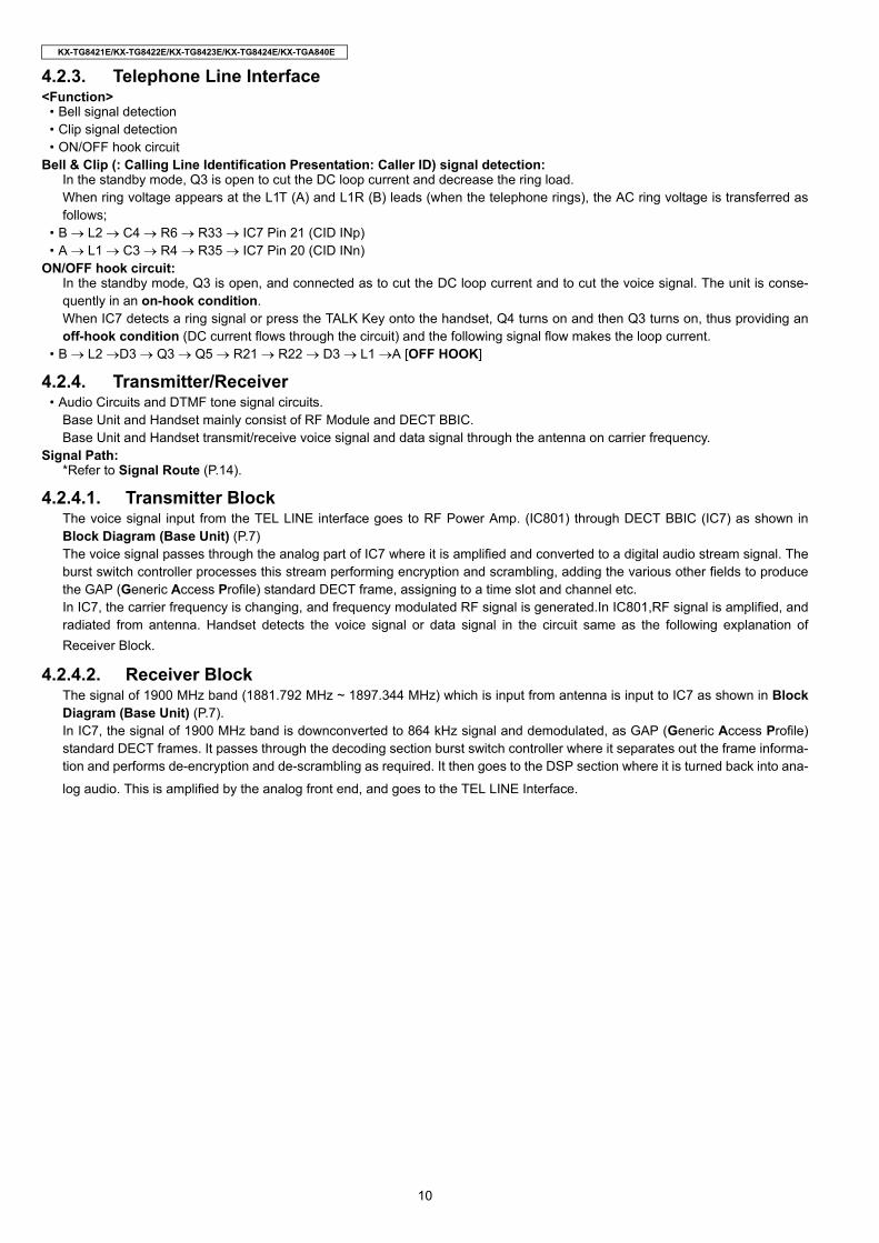
4.2.3. Telephone Line Interface<Function>
• Bell signal detection• Clip signal detection• ON/OFF hook circuit
Bell & Clip (: Calling Line Identification Presentation: Caller ID) signal detection:In the standby mode, Q3 is open to cut the DC loop current and decrease the ring load.When ring voltage appears at the L1T (A) and L1R (B) leads (when the telephone rings), the AC ring voltage is transferred asfollows;
• B → L2 → C4 → R6 → R33 → IC7 Pin 21 (CID INp) • A → L1 → C3 → R4 → R35 → IC7 Pin 20 (CID INn)
ON/OFF hook circuit:In the standby mode, Q3 is open, and connected as to cut the DC loop current and to cut the voice signal. The unit is conse-quently in an on-hook condition. When IC7 detects a ring signal or press the TALK Key onto the handset, Q4 turns on and then Q3 turns on, thus providing anoff-hook condition (DC current flows through the circuit) and the following signal flow makes the loop current.
• B → L2 →D3 → Q3 → Q5 → R21 → R22 → D3 → L1 →A [OFF HOOK]
4.2.4. Transmitter/Receiver• Audio Circuits and DTMF tone signal circuits.
Base Unit and Handset mainly consist of RF Module and DECT BBIC. Base Unit and Handset transmit/receive voice signal and data signal through the antenna on carrier frequency.
Signal Path:*Refer to Signal Route (P.14).
4.2.4.1. Transmitter BlockThe voice signal input from the TEL LINE interface goes to RF Power Amp. (IC801) through DECT BBIC (IC7) as shown inBlock Diagram (Base Unit) (P.7)The voice signal passes through the analog part of IC7 where it is amplified and converted to a digital audio stream signal. Theburst switch controller processes this stream performing encryption and scrambling, adding the various other fields to producethe GAP (Generic Access Profile) standard DECT frame, assigning to a time slot and channel etc.In IC7, the carrier frequency is changing, and frequency modulated RF signal is generated.In IC801,RF signal is amplified, andradiated from antenna. Handset detects the voice signal or data signal in the circuit same as the following explanation ofReceiver Block.
4.2.4.2. Receiver BlockThe signal of 1900 MHz band (1881.792 MHz ~ 1897.344 MHz) which is input from antenna is input to IC7 as shown in BlockDiagram (Base Unit) (P.7).In IC7, the signal of 1900 MHz band is downconverted to 864 kHz signal and demodulated, as GAP (Generic Access Profile)standard DECT frames. It passes through the decoding section burst switch controller where it separates out the frame informa-tion and performs de-encryption and de-scrambling as required. It then goes to the DSP section where it is turned back into ana-
log audio. This is amplified by the analog front end, and goes to the TEL LINE Interface.

11
KX-TG8421E/KX-TG8422E/KX-TG8423E/KX-TG8424E/KX-TGA840E
4.3. Block Diagram (Handset)
SP
EA
KE
R
RE
CE
IVE
R
MIC
MIC
DE
T
SP
HE
AD
SE
T
CH
AR
GE
CIR
CU
ITQ
4,
Q9
, R
7Q
4,
Q9
,R
7
CH
AR
GE
CO
NT
AC
TS
CH
AR
GE
(+)
CH
AR
GE
(-)
CH
AR
GE
_C
TR
L
CH
AR
GE
EE
PR
OM
SC
L
SD
A
BA
TT
ER
YT
ER
MIN
AL
D7
VB
AT
J1 J2
1.8
VQ
21.8
V
LC
D
CD
RE
SE
TC
SB
SD
A
SC
L
CP
U
An
alo
gF
ron
tE
nd
D/A
A/D
33
35 15
16
19
20
18
28
32
31
57
58
36 13
43
42
63
54
55
66
AD
PC
MC
od
ec
Filt
er
DS
P
Speech
Deco
din
g
Speech
Enco
din
g
BM
C
Burs
tD
eco
din
g
RF
PA
IC801
Burs
tE
nco
din
g
RF
PLL
MO
D/D
EM
OD
5 3
4 3 6 789
2 77
7875
RX
n
RX
on
AN
T
DA
80
1R
Xp
TX
p
TX
n
Po
nP
SE
L
TX
on
VD
D-P
AD
RY
9 10
XT
AL
X1 1
0.3
68
MH
zB
AT
TE
RY
44
ON
SW
ITC
H
KE
YP
AD
Ch
arg
eP
um
p
RO
WS
CO
LU
MN
S
CP
2.5
VC
P4
.0V
48
, 4
9,
50
, 5
1
22
, 2
3,
24
, 2
5,
26
BB
ICIC
1
IC3
56
LC
D-B
AC
K
LIG
HT
KE
Y
LE
D
BE
LL
L
ED
42
52
68
73
74
80
LD
O_
CT
RL
KX
-TG
A8
40
BL
OC
K D
IAG
RA
M (
HA
ND
SE
T)
12
KX-TG8421E/KX-TG8422E/KX-TG8423E/KX-TG8424E/KX-TGA840E
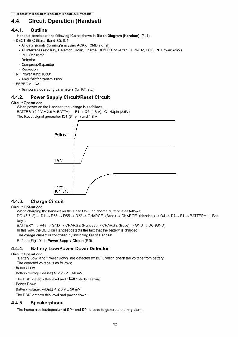
4.4. Circuit Operation (Handset)4.4.1. Outline
Handset consists of the following ICs as shown in Block Diagram (Handset) (P.11).• DECT BBIC (Base Band IC): IC1
- All data signals (forming/analyzing ACK or CMD signal)- All interfaces (ex: Key, Detector Circuit, Charge, DC/DC Converter, EEPROM, LCD, RF Power Amp.)- PLL Oscillator- Detector- Compress/Expander- Reception
• RF Power Amp: IC801- Amplifier for transmission
• EEPROM: IC3- Temporary operating parameters (for RF, etc.)
4.4.2. Power Supply Circuit/Reset CircuitCircuit Operation:
When power on the Handset, the voltage is as follows;BATTERY(2.2 V ~ 2.6 V: BATT+) → F1 → Q2 (1.8 V), IC1-43pin (2.5V)The Reset signal generates IC1 (61 pin) and 1.8 V.
4.4.3. Charge CircuitCircuit Operation:
When charging the handset on the Base Unit, the charge current is as follows;DC+(6.5 V) → D1 → R56 → R55 → D22 → CHARGE+(Base) → CHARGE+(Handset) → Q4 → D7→ F1 → BATTERY+... Bat-tery... BATTERY- → R45 → GND → CHARGE-(Handset)→ CHARGE-(Base) → GND → DC-(GND)In this way, the BBIC on Handset detects the fact that the battery is charged.The charge current is controlled by switching Q9 of Handset.Refer to Fig.101 in Power Supply Circuit (P.9).
4.4.4. Battery Low/Power Down DetectorCircuit Operation:
“Battery Low” and “Power Down” are detected by BBIC which check the voltage from battery.The detected voltage is as follows;
• Battery LowBattery voltage: V(Batt) 2.25 V ± 50 mV
The BBIC detects this level and " " starts flashing.• Power Down
Battery voltage: V(Batt) 2.0 V ± 50 mVThe BBIC detects this level and power down.
4.4.5. SpeakerphoneThe hands-free loudspeaker at SP+ and SP- is used to generate the ring alarm.

13
KX-TG8421E/KX-TG8422E/KX-TG8423E/KX-TG8424E/KX-TGA840E
4.5. Circuit Operation (Charger Unit)4.5.1. Power Supply CircuitThe power supply is as shown.

14
KX-TG8421E/KX-TG8422E/KX-TG8423E/KX-TG8424E/KX-TGA840E
4.6. Signal Route

15
KX-TG8421E/KX-TG8422E/KX-TG8423E/KX-TG8424E/KX-TGA840E

16
KX-TG8421E/KX-TG8422E/KX-TG8423E/KX-TG8424E/KX-TGA840E
5 Location of Controls and Components
5.1. Controls5.1.1. Base Unit
5.1.2. Handset

17
KX-TG8421E/KX-TG8422E/KX-TG8423E/KX-TG8424E/KX-TGA840E
6 Installation Instructions6.1. Connections
6.2. Battery6.2.1. Battery Installation
See For Service Hint (P.28)
6.2.2. Battery Charge

18
KX-TG8421E/KX-TG8422E/KX-TG8423E/KX-TG8424E/KX-TGA840E
Note for service:The battery strength may not be indicated correctly if thebattery is disconnected and connected again, even after it isfully charged. In that case, by recharging the battery asmentioned above, you will get a correct indication of thebattery strength.
6.2.3. Battery Level
6.2.4. Panasonic Ni-MH Battery Performance (supplied batteries)

19
KX-TG8421E/KX-TG8422E/KX-TG8423E/KX-TG8424E/KX-TGA840E
7 Operating Instructions7.1. Programmable SettingsYou can customise the unit by programming the following features using the handset.
7.1.1. Programming by scrolling through the display menus

20
KX-TG8421E/KX-TG8422E/KX-TG8423E/KX-TG8424E/KX-TGA840E
*1 The item will not be reset when pressing , , and keys. Refer to How to Clear User Setting (P.35).
*2 The item will not be reset when pressing , , and keys. Refer to How to Clear User Setting (P.35).
Cross Reference:Registering a Handset to a Base Unit (P.22)
7.1.2. Answering System Setting

21
KX-TG8421E/KX-TG8422E/KX-TG8423E/KX-TG8424E/KX-TGA840E
7.1.3. SMS Setting
Note:(*1) If the password of a private mailbox is forgotten, refer to For Service Hint (P.28)
22
KX-TG8421E/KX-TG8422E/KX-TG8423E/KX-TG8424E/KX-TGA840E
7.2. Registering a Handset to a Base Unit
If you forget your PIN, see "Programmable settings" in Troubleshooting (P.24)
Note:• When you purchase an additional handset, refer to the additional handset's installation manual for registration.
7.2.1. Deregistering a Handset
7.2.2. Cancelling a base unit
Cross Reference:Registering a Handset to a Base Unit (P.22)
23
KX-TG8421E/KX-TG8422E/KX-TG8423E/KX-TG8424E/KX-TGA840E
7.3. Copying Phonebook EntriesYou can copy phonebook entries to the phonebook of another compatible Panasonic handset.
Note:• Category settings for phonebook entries are not copied.
7.3.1. Copying all entries
7.4. Error Messages
24
KX-TG8421E/KX-TG8422E/KX-TG8423E/KX-TG8424E/KX-TGA840E
7.5. Troubleshooting

25
KX-TG8421E/KX-TG8422E/KX-TG8423E/KX-TG8424E/KX-TGA840E

26
KX-TG8421E/KX-TG8422E/KX-TG8423E/KX-TG8424E/KX-TGA840E

27
KX-TG8421E/KX-TG8422E/KX-TG8423E/KX-TG8424E/KX-TGA840E

28
KX-TG8421E/KX-TG8422E/KX-TG8423E/KX-TG8424E/KX-TGA840E
7.6. For Service Hint
Cross Reference:Battery Charge (P.17)Frequently Used Items (Base Unit) (P.30)
29
KX-TG8421E/KX-TG8422E/KX-TG8423E/KX-TG8424E/KX-TGA840E
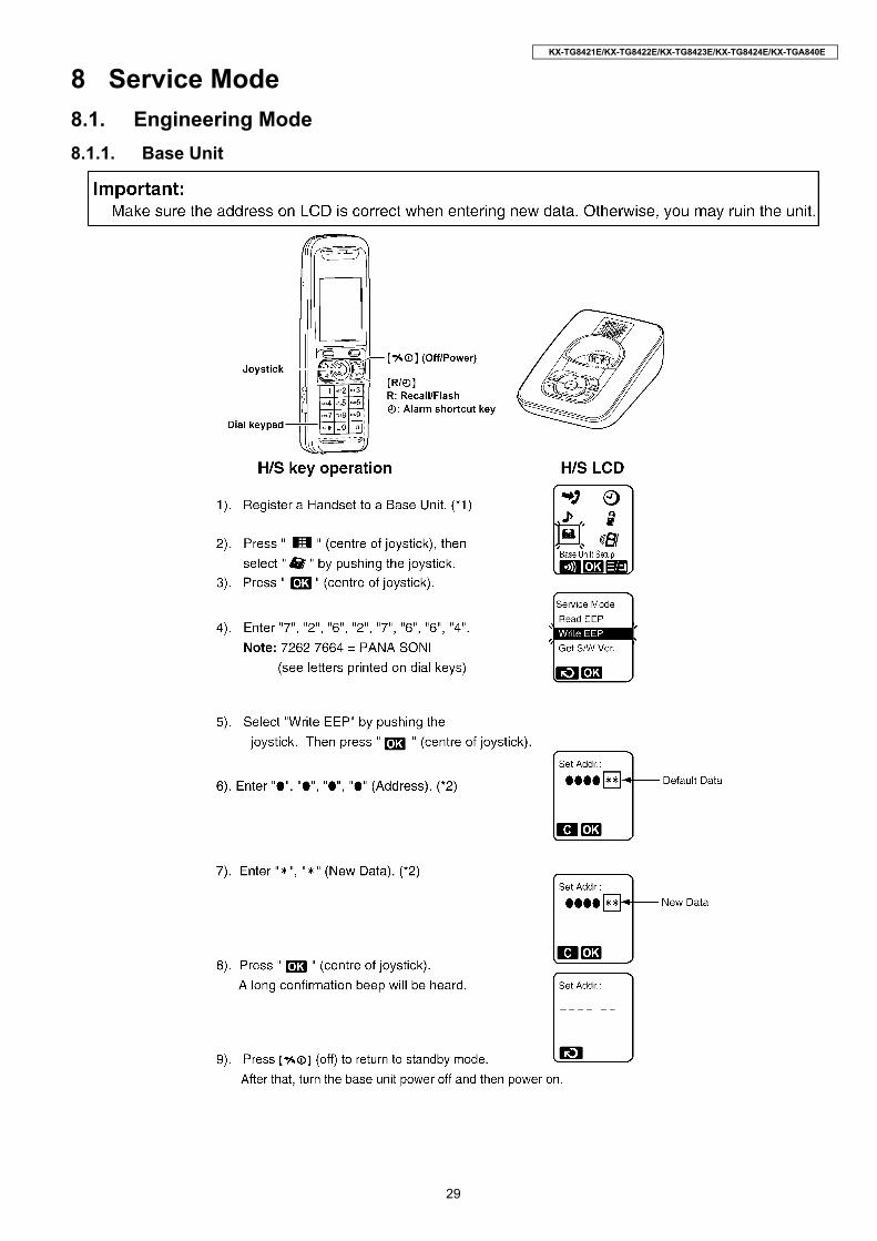
8 Service Mode8.1. Engineering Mode8.1.1. Base Unit
30
KX-TG8421E/KX-TG8422E/KX-TG8423E/KX-TG8424E/KX-TGA840E
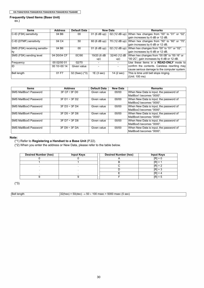
Frequently Used Items (Base Unit)ex.)
Note:(*1) Refer to Registering a Handset to a Base Unit (P.22).(*2) When you enter the address or New Data, please refer to the table below.
(*3)
Items Address Default Data New Data RemarksC-ID (FSK) sensitivity 04 B6 00 01 (6 dB up) 02 (12 dB up) When hex changes from “00” to “01” or “02”,
gain increases by 6 dB or 12 dB.C-ID (DTMF) sensitivity 04 C4 50 60 (6 dB up) 70 (12 dB up) When hex changes from “50” to “60” or “70”,
gain increases by 6 dB or 12 dB.SMS (FSK) receiving sensitiv-ity
04 B6 00 01 (6 dB up) 02 (12 dB up) When hex changes from “00” to “01” or “02”, gain increases by 6 dB or 12 dB.
SMS (FSK) sending level 04 D0/04 CF 0C/90 19/20 (6 dB up)
32/40 (12 dB up)
When hex changes from “00 0B” to “00 16” or “00 2C”, gain increases by 6 dB or 12 dB.
Frequency 00 02/00 01 02/70 - - Use these items in a READ-ONLY mode toconfirm the contents. Careless rewriting maycause serious damage to the computer system.
ID 00 10~00 14 Given value - -
Bell length 01 F7 32 (5sec) (*3) 1E (3 sec) 14 (2 sec) This is time until bell stops ringing.(Unit: 100 ms)
Items Address Default Data New Data RemarksSMS MailBox1 Password 3F CF / 3F D0 Given value 00/00 When New Data is input, the password of
MailBox1 becomes “0000”.SMS MailBox2 Password 3F D1 ~ 3F D2 Given value 00/00 When New Data is input, the password of
MailBox2 becomes “0000”.SMS MailBox3 Password 3F D3 ~ 3F D4 Given value 00/00 When New Data is input, the password of
MailBox3 becomes “0000”.SMS MailBox4 Password 3F D5 ~ 3F D6 Given value 00/00 When New Data is input, the password of
MailBox4 becomes “0000”.SMS MailBox5 Password 3F D7 ~ 3F D8
Given value 00/00 When New Data is input, the password of
MailBox5 becomes “0000”.SMS MailBox6 Password 3F D9 ~ 3F DA Given value 00/00 When New Data is input, the password of
MailBox6 becomes “0000”.
Desired Number (hex) Input Keys Desired Number (hex) Input Keys0 0 A [R] + 01 1 B [R] + 1. . C [R] + 2. . D [R] + 3. . E [R] + 49 9 F [R] + 5
Bell length 32(hex) = 50(dec) → 50 × 100 msec = 5000 msec (5 sec)
31
KX-TG8421E/KX-TG8422E/KX-TG8423E/KX-TG8424E/KX-TGA840E
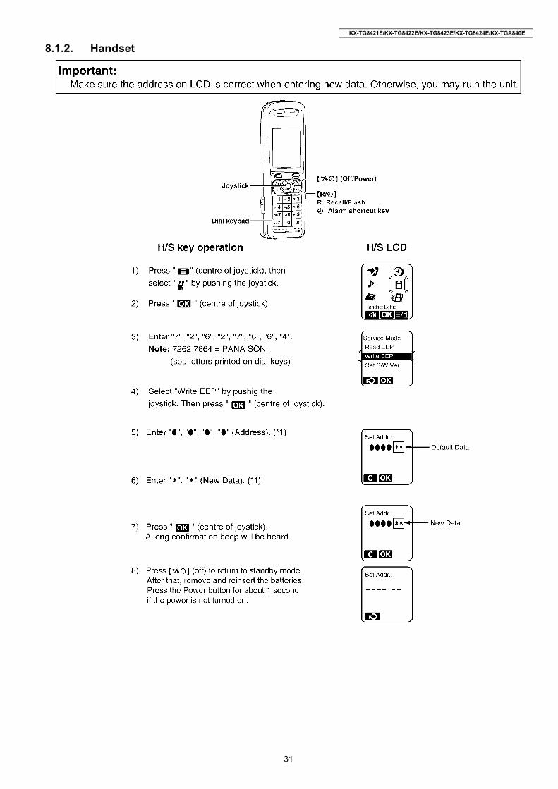
8.1.2. Handset

32
KX-TG8421E/KX-TG8422E/KX-TG8423E/KX-TG8424E/KX-TGA840E
Frequently Used Items (Handset)ex.)
Note:(*1) When you enter the address or New Data, please refer to the table below.
(*2) When adding “01” (hex) to default value, sending level increases by 0.25 dB.ex.)
(*3) When reducing “01” (hex) from default value, receiving level increases by 0.25 dB.ex.)
(*4) Use these items in a READ-ONLY mode to confirm the contents. Careless rewriting may cause serious damage to thehandset.
Items Address Default Data New Data Possible AdjustedValue MAX (hex)
Possible AdjustedValue MIN (hex)
Remarks
Sending level 00 06 Adjusted value Given value 6F 00 (*2)Receiving level 00 07 Adjusted value Given value 00 3F (*3)
Battery Low 00 04 70 - - -(*4)Frequency 00 02/00 01 02/70 - - -
ID 00 10~00 14 Given value - - -
Desired Number (hex.) Input Keys Desired Number (hex.) Input Keys0 0 A [R] + 01 1 B [R] + 1. . C [R] + 2. . D [R] + 3. . E [R] + 49 9 F [R] + 5
Item Default Data New Data3A 3E 36
Sending level -8dBm -7dBm -9dBm
Item Default Data New Data14 18 10
Receiving level -22dBm -23dBm -21dBm

33
KX-TG8421E/KX-TG8422E/KX-TG8423E/KX-TG8424E/KX-TGA840E
8.2. Copying Phonebook Items when RepairingYou can copy the handset phonebook to another (compatible Panasonic) handset. This will help to save the original phonebookdata which the customer has registered.Available models: KX-TG8421/KX-TG8422/KX-TG8423/KX-TG8424Refer to the following procedures.
Note:• BS=Base Unit , HS=Handset• If the max number of handsets are already registered to the base unit, a new handset cannot be registered.• To register the handset, refer to Registering a Handset to a
Base Unit (P.22)• To cancel the handset, refer to Deregistering a Handset
(P.22)• To copy the handset phonebook, refer to Copying Phone-
book Entries (P.24)

34
KX-TG8421E/KX-TG8422E/KX-TG8423E/KX-TG8424E/KX-TGA840E
Note:• BS=Base Unit , HS=Handset• If the max number of handsets are already registered to the base unit, a new handset cannot be registered.• To register the handset, refer to Registering a Handset to a Base Unit (P.22)• To cancel the handset, refer to Deregistering a Handset (P.22)
• To copy the handset phonebook, refer to Copying Phonebook Entries (P.24)

35
KX-TG8421E/KX-TG8422E/KX-TG8423E/KX-TG8424E/KX-TGA840E
8.3. How to Clear User SettingUnits are reset to the Factory settings by this operation (Erase recorded Voice messages*, stored Phone numbers, Caller listand etc.)
Note:• Some menus are not reset. Refer to Operating Instructions (P.19).• The reset menus differ depending on the following operations.• This operation should not be performed for a usual repair.
* KX-TG8421/KX-TG8422/KX-TG8423/KX-TG8424 only
8.3.1. Resetting both base unit and handsetBoth the base unit and the registered handset which you did the following steps to are reset. Other registered handsetswill not be reset.
Note:(*1) Refer to Registering a Handset to a Base Unit (P.22).
8.3.2. Resetting only handsetThe only handset is reset by doing the following steps to .
Note: (*2)• The handset registration to the base unit is cancelled.• If the handset needs to be registered to the base unit, refer to Registering a Handset to a Base Unit (P.22).
• If users do not bring the base unit with them, the registration procedure has to be done by users themselves.
36
KX-TG8421E/KX-TG8422E/KX-TG8423E/KX-TG8424E/KX-TGA840E
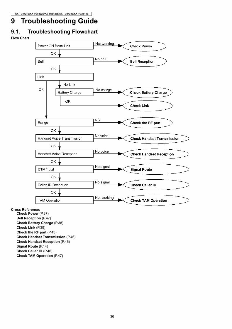
9 Troubleshooting Guide9.1. Troubleshooting FlowchartFlow Chart
Cross Reference:Check Power (P.37)Bell Reception (P.47)Check Battery Charge (P.38)Check Link (P.39)Check the RF part (P.43)Check Handset Transmission (P.46)Check Handset Reception (P.46)Signal Route (P.14)Check Caller ID (P.46)Check TAM Operation (P.47)

37
KX-TG8421E/KX-TG8422E/KX-TG8423E/KX-TG8424E/KX-TGA840E
9.1.1. Check Power9.1.1.1. Base Unit
Is the AC Adaptor inserted into AC outlet? (*1)
Cross Reference:Power Supply Circuit (P.9)
Note:(*1) Refer to Specifications (P.6) for part number and supply voltage of AC Adaptor.
9.1.1.2. Handset
Cross Reference:Power Supply Circuit/Reset Circuit (P.12)

38
KX-TG8421E/KX-TG8422E/KX-TG8423E/KX-TG8424E/KX-TGA840E
9.1.2. Check Battery Charge9.1.2.1. Base Unit
Cross Reference:Charge Circuit (P.12)
9.1.2.2. Handset
Cross Reference:Check Power (P.37)Charge Circuit (P.12)
9.1.2.3. Charger Unit
Cross Reference:Charge Circuit (P.12)
39
KX-TG8421E/KX-TG8422E/KX-TG8423E/KX-TG8424E/KX-TGA840E
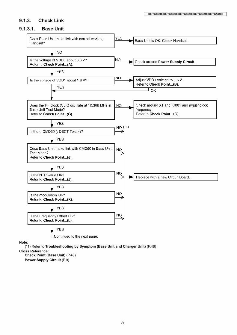
9.1.3. Check Link9.1.3.1. Base Unit
Note:(*1) Refer to Troubleshooting by Symptom (Base Unit and Charger Unit) (P.48)
Cross Reference:Check Point (Base Unit) (P.48)Power Supply Circuit (P.9)

40
KX-TG8421E/KX-TG8422E/KX-TG8423E/KX-TG8424E/KX-TGA840E
Cross Reference:Check Point (Base Unit) (P.48)

41
KX-TG8421E/KX-TG8422E/KX-TG8423E/KX-TG8424E/KX-TGA840E
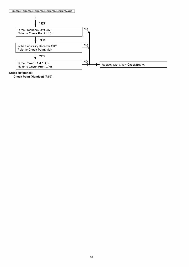
9.1.3.2. Handset
Cross Reference:Check Point (Handset) (P.52)Power Supply Circuit/Reset Circuit (P.12)
42
KX-TG8421E/KX-TG8422E/KX-TG8423E/KX-TG8424E/KX-TGA840E
Cross Reference:Check Point (Handset) (P.52)

43
KX-TG8421E/KX-TG8422E/KX-TG8423E/KX-TG8424E/KX-TGA840E
9.1.4. Check the RF part9.1.4.1. Finding out the Defective part
After All the Checkings or Repairing1. Re-register the checked Handset to the checked Base Unit, and Regular HS to Regular BU.
Note:If you need to register a handset, refer to Registering a Handset to a Base Unit (P.22)
44
KX-TG8421E/KX-TG8422E/KX-TG8423E/KX-TG8424E/KX-TGA840E
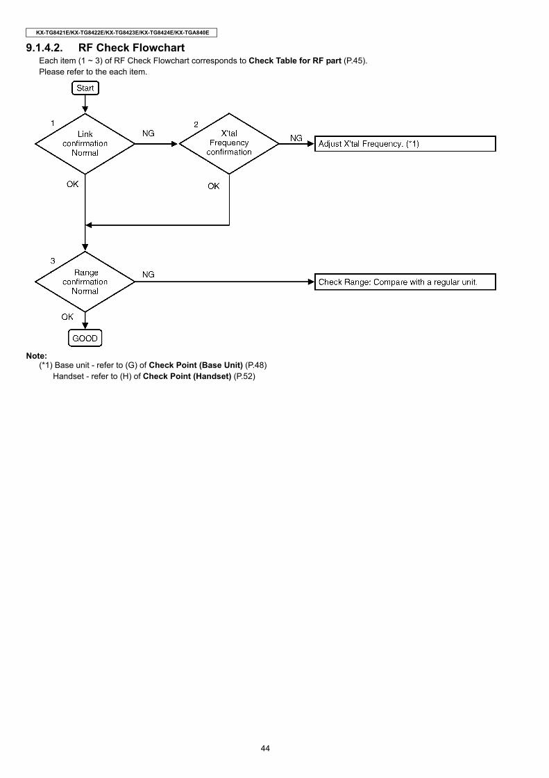
9.1.4.2. RF Check FlowchartEach item (1 ~ 3) of RF Check Flowchart corresponds to Check Table for RF part (P.45).Please refer to the each item.
Note:(*1) Base unit - refer to (G) of Check Point (Base Unit) (P.48) Handset - refer to (H) of Check Point (Handset) (P.52)
45
KX-TG8421E/KX-TG8422E/KX-TG8423E/KX-TG8424E/KX-TGA840E
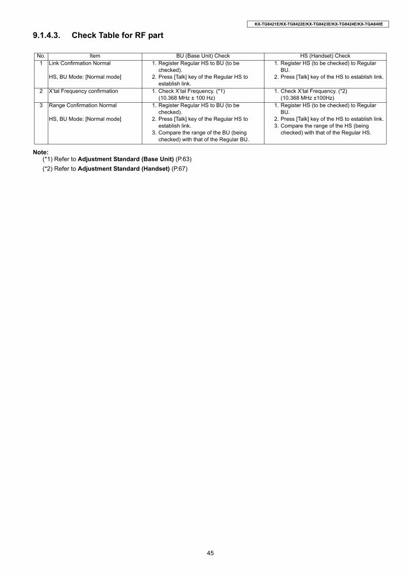
9.1.4.3. Check Table for RF part
Note:(*1) Refer to Adjustment Standard (Base Unit) (P.63)(*2) Refer to Adjustment Standard (Handset) (P.67)
No. Item BU (Base Unit) Check HS (Handset) Check1 Link Confirmation Normal
HS, BU Mode: [Normal mode]
1. Register Regular HS to BU (to be checked).
2. Press [Talk] key of the Regular HS to establish link.
1. Register HS (to be checked) to Regular BU.
2. Press [Talk] key of the HS to establish link.
2 X’tal Frequency confirmation 1. Check X’tal Frequency. (*1)(10.368 MHz ± 100 Hz)
1. Check X’tal Frequency. (*2)(10.368 MHz ±100Hz)
3 Range Confirmation Normal
HS, BU Mode: [Normal mode]
1. Register Regular HS to BU (to be checked).
2. Press [Talk] key of the Regular HS to establish link.
3. Compare the range of the BU (being checked) with that of the Regular BU.
1. Register HS (to be checked) to Regular BU.
2. Press [Talk] key of the HS to establish link.3. Compare the range of the HS (being
checked) with that of the Regular HS.
46
KX-TG8421E/KX-TG8422E/KX-TG8423E/KX-TG8424E/KX-TGA840E
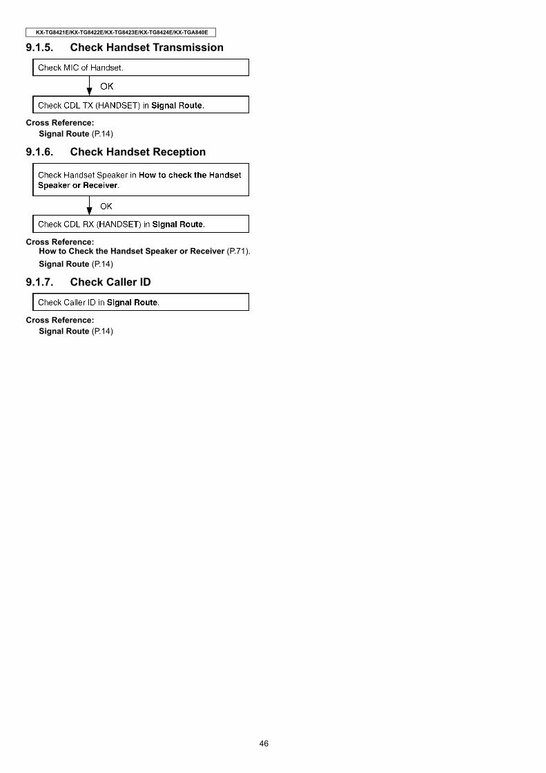
9.1.5. Check Handset Transmission
Cross Reference:Signal Route (P.14)
9.1.6. Check Handset Reception
Cross Reference:How to Check the Handset Speaker or Receiver (P.71).Signal Route (P.14)
9.1.7. Check Caller ID
Cross Reference:Signal Route (P.14)
47
KX-TG8421E/KX-TG8422E/KX-TG8423E/KX-TG8424E/KX-TGA840E
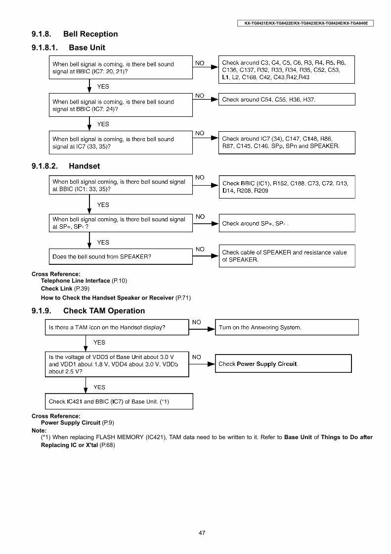
9.1.8. Bell Reception9.1.8.1. Base Unit
9.1.8.2. Handset
Cross Reference:Telephone Line Interface (P.10)Check Link (P.39)How to Check the Handset Speaker or Receiver (P.71)
9.1.9. Check TAM Operation
Cross Reference:Power Supply Circuit (P.9)
Note:(*1) When replacing FLASH MEMORY (IC421), TAM data need to be written to it. Refer to Base Unit of Things to Do afterReplacing IC or X'tal (P.68)
48
KX-TG8421E/KX-TG8422E/KX-TG8423E/KX-TG8424E/KX-TGA840E
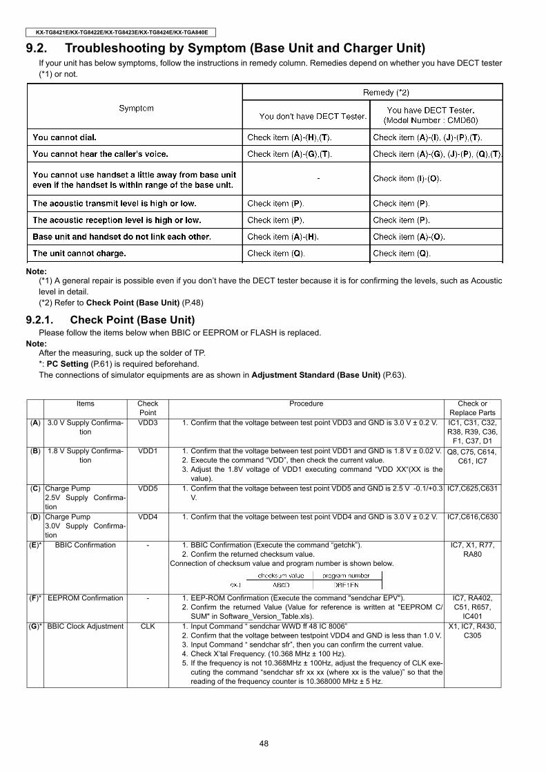
9.2. Troubleshooting by Symptom (Base Unit and Charger Unit)If your unit has below symptoms, follow the instructions in remedy column. Remedies depend on whether you have DECT tester(*1) or not.
Note:(*1) A general repair is possible even if you don’t have the DECT tester because it is for confirming the levels, such as Acousticlevel in detail.(*2) Refer to Check Point (Base Unit) (P.48)
9.2.1. Check Point (Base Unit)Please follow the items below when BBIC or EEPROM or FLASH is replaced.
Note:After the measuring, suck up the solder of TP.*: PC Setting (P.61) is required beforehand.The connections of simulator equipments are as shown in Adjustment Standard (Base Unit) (P.63).
Items Check Point
Procedure Check or Replace Parts
(A) 3.0 V Supply Confirma-tion
VDD3 1. Confirm that the voltage between test point VDD3 and GND is 3.0 V ± 0.2 V. IC1, C31, C32, R38, R39, C36,
F1, C37, D1(B) 1.8 V Supply Confirma-
tionVDD1 1. Confirm that the voltage between test point VDD1 and GND is 1.8 V ± 0.02 V.
2. Execute the command “VDD”, then check the current value.3. Adjust the 1.8V voltage of VDD1 executing command “VDD XX“(XX is the
value).
Q8, C75, C614, C61, IC7
(C) Charge Pump2.5V Supply Confirma-tion
VDD5 1. Confirm that the voltage between test point VDD5 and GND is 2.5 V -0.1/+0.3V.
IC7,C625,C631
(D) Charge Pump3.0V Supply Confirma-tion
VDD4 1. Confirm that the voltage between test point VDD4 and GND is 3.0 V ± 0.2 V. IC7,C616,C630
(E)* BBIC Confirmation - 1. BBIC Confirmation (Execute the command “getchk”).2. Confirm the returned checksum value.
Connection of checksum value and program number is shown below.
IC7, X1, R77, RA80
(F)* EEPROM Confirmation - 1. EEP-ROM Confirmation (Execute the command "sendchar EPV").2. Confirm the returned Value (Value for reference is written at "EEPROM C/
SUM" in Software_Version_Table.xls).
IC7, RA402, C51, R657,
IC401(G)* BBIC Clock Adjustment CLK 1. Input Command “ sendchar WWD ff 48 IC 8006”
2. Confirm that the voltage between testpoint VDD4 and GND is less than 1.0 V.3. Input Command “ sendchar sfr”, then you can confirm the current value.4. Check X’tal Frequency. (10.368 MHz ± 100 Hz).5. If the frequency is not 10.368MHz ± 100Hz, adjust the frequency of CLK exe-
cuting the command “sendchar sfr xx xx (where xx is the value)” so that thereading of the frequency counter is 10.368000 MHz ± 5 Hz.
X1, IC7, R430, C305

49
KX-TG8421E/KX-TG8422E/KX-TG8423E/KX-TG8424E/KX-TGA840E
(H)* Hookswitch Check with DC Characteristics
- 1. Connect Telephone Socket to Tel-simulator which is connected with 600 Ω.2. Set line voltage to 48 V and line current to 40mA at off-hook condition of nor-
mal telephone.3. Execute the command “hookoff”4. Confirm that the line current is 40 mA ± 5 mA.5. Execute the command “hookon”.6. Confirm that the line current is less than + 0.8 mA.
L1, L2, Q3, R14, R15, Q4, R16,
R17, D3, R18~R24,
C15~C17, D21, Q5, R27, IC7
(I) DTMF Generator Check - 1. Connect Telephone Socket to DTMF tester. (Load=600 Ω)2. Link Handset and push dial key.3. Confirm DTMF character.4. Confirm that the high Group is -6.0 dBm ~ -10.0 dBm.5. Confirm that the low Group is -8.5 dBm ~ -12.5 dBm.
IC7, R116, C141, R29, C22,
C23, Q5, D21
(J)* Transmitted Power Con-firmation
-ANTI_TP
Remove the Antenna before starting step from 1 to 7.1. Configure the DECT tester (CMD60) as follows;
<Setting>• Test mode: FP• Traffic Carrier: 5• Traffic Slot: 4• Mode: Loopback• PMID: 00000• RF LEVEL = -70 dBm.
2. Execute the command ”sendchar TST”.3. Execute the command “sendchar dmv 2 2”.4. Check that “Signalling Status” has been set to “Locked”, then press “ACCEPT
RFPI”.5. Initiate connection from Dect tester (“set up connect”)6. Execute the command “ANT1”.7. Confirm that the NTP value at ANT is 19.0 dBm ~ 25.0 dBm.
IC7, C802~C806, C808~C814, C820, C819, C822, C823, C825, C827, C826, C834, C851, C853, C859~C861,
DA801, DA802, IC801,
L801~L803, C855~C858, R801~R807, R106, R109,
Q9, C617 (K)* Modulation Check and
Adjustment-
ANTI_TPFollow steps 1 to 6 of (J).
7.Confirm that the B-Field Modulation is -370 ± 30/ +370± 30 kHz/div & Modu-lated width 690 kHz using data type Fig31.8.Adjust the B-Field Modulation if required. (Execute the command “readmod”and “wrtmod xx”, where xx is the value.)
IC7, C802~C806, C808~C814, C820, C819, C822, C823, C825, C827, C826, C834, C851, C853, C859~C861,
DA801, DA802, IC801,
L801~L803, C855~C858, R801~R807, R106, R109,
Q9, C617 (L)* Frequency Offset Check -
ANTI_TPFollow steps 1 to 6 of (J).
7.Confirm that the frequency offset is < ± 50 kHz.IC7,
C802~C806, C808~C814, C820, C819, C822, C823, C825, C827, C826, C834, C851, C853, C859~C861,
DA801, DA802, IC801,
L801~L803, C855~C858, R801~R807, R106, R109,
Q9, C617
Items Check Point
Procedure Check or Replace Parts

50
KX-TG8421E/KX-TG8422E/KX-TG8423E/KX-TG8424E/KX-TGA840E
(M)* Frequency Drift Confir-mation
-ANTI_TP
Follow steps 1 to 6 of (J).7.Confirm that the frequency drift is < ± 35 kHz/ms.
IC7, C802~C806, C808~C814, C820, C819, C822, C823, C825, C827, C826, C834, C851, C853, C859~C861,
DA801, DA802, IC801,
L801~L803, C855~C858, R801~R807, R106, R109,
Q9, C617 (N)* Sensitivity Receiver
Confirmation-
ANTI_TPFollow steps 1 to 6 of (J).
7.Set DECT tester power to -90 dBm.8.Confirm that the BER is < 1000 ppm.
IC7, C802~C806, C808~C814, C820, C819, C822, C823, C825, C827, C826, C834, C851, C853, C859~C861,
DA801, DA802, IC801,
L801~L803, C855~C858, R801~R807, R106, R109,
Q9, C617 (O)* Timing Confirmation -
ANTI_TPFollow steps 1 to 6 of (J).
7.Confirm that the Timing accuracy is• ± 5.0 ppm (When adjust the frequency of CLK in item (G)).• ± 15 ppm (When do not adjust the frequency of CLK in item (A)).
IC7, C802~C806, C808~C814, C820, C819, C822, C823, C825, C827, C826, C834, C851, C853, C859~C861,
DA801, DA802, IC801,
L801~L803, C855~C858, R801~R807, R106, R109,
Q9, C617 (P)* Power RAMP Confirma-
tion- Follow steps 1 to 6 of (J).
7.Confirm that Power RAMP is matching.IC7,
C802~C806, C808~C814, C820, C819, C822, C823, C825, C827, C826, C834, C851, C853, C859~C861,
DA801, DA802, IC801,
L801~L803, C855~C858, R801~R807, R106, R109,
Q9, C617
Items Check Point
Procedure Check or Replace Parts

51
KX-TG8421E/KX-TG8422E/KX-TG8423E/KX-TG8424E/KX-TGA840E
9.2.2. Check Point (Charger Unit)
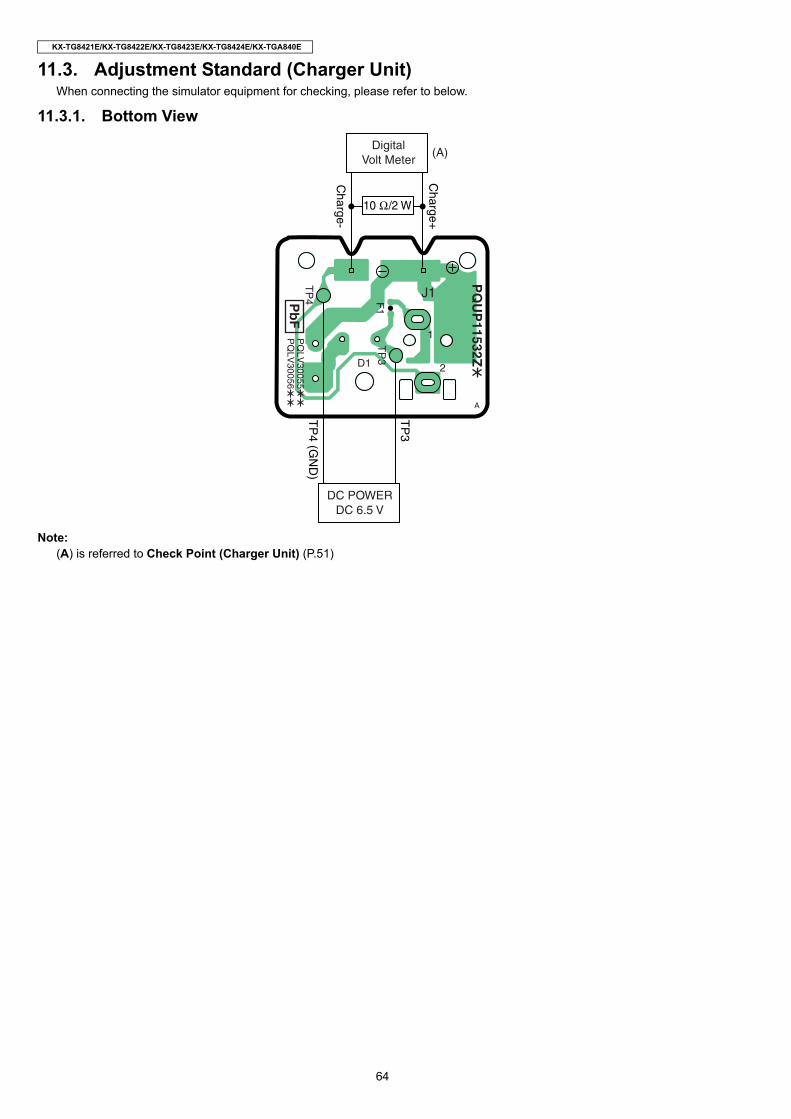
Note:After the measuring, suck up the solder of TP.The connection of adjustment equipment is as shown in Adjustment Standard (Charger Unit) (P.64).
(Q) Audio Check - 1. Link with Handset.2. Input -45dBm/1kHz to MIC of Handset.
Measure the Level at Line I/F and distortion level.3. Confirm that the level is -8 dBm ± 2 dBm and that the distortion level is < 5%
at TEL Line (600 Ω Load).4. Input -20 dBm/1 kHz to Line I/F.
Measure the level at Receiver of Handset and distortion level(*Receive volume set to second position from minimum).
5. Confirm that the level is -22 dBm ± 2 dBm and that the distortion level is < 5%at Receiver (Volume Middle, 150 Ω Load).
IC7, SA1, L1, L2, D3, Q3, Q4, R14, R15, R16, R17, D21, Q5, R19, R20, C14,
C56, R117, R116, C141, R9,
C22, C23
(R) Charging Check - 1. Connect Charge Contact 12 Ω/2 W resistor between charge+ and charge-.2. Measure and confirm voltage across the resistor is 3.10 V ± 0.3 V.
R55, R56, D22, D23
(S) TAM Operation Confir-mation
- 1. TAM Confirmation (Execute the command "sendchar VPI").2. Confirm the returned Value (Value is "DAS7EA 03").
IC7, IC421, R424~R429, C421, C422,
Q421(T) 2.4V Supply Confirma-
tion VDD2 VDD2 1. Confirm that the voltage between test point VDD2 and GND is 2.5V ± 0.2V. IC7, Q9, C617
Items Check Point
Procedure Check or Replace Parts
(A) Charging Check - 1. Connect Charge Contact 10Ω/2 W resistor between charge+ and charge-.2. Measure and confirm voltage across the resistor is 3.1 V ± 0.3 V.
R1 D1, F1
Items Check Point
Procedure Check or Replace Parts

52
KX-TG8421E/KX-TG8422E/KX-TG8423E/KX-TG8424E/KX-TGA840E
9.3. Troubleshooting by Symptom (Handset)If your unit has below symptoms, follow the instructions in remedy column. Remedies depend on whether you have DECT tester(*1) or not.
Note:(*1) A general repair is possible even if you don’t have the DECT tester because it is for confirming the levels, such as Acousticlevel in detail.(*2) Refer to Check Point (Handset) (P.52)
9.3.1. Check Point (Handset)Please follow the items below when BBIC or EEPROM is replaced.
Note:After the measuring, suck up the solder of TP.*: PC Setting (P.65) is required beforehand.The connections of adjustment equipments are as shown in Adjustment Standard (Handset) (P.67).
Items Check Point
Procedure Check or Replace Parts
(A)* 1.8 V Supply Adjustment VDD1 1. Confirm that the voltage between test point VDD1 and GND is 1.8 V ± 0.02 V.2. Execute the command “VDD”, then check the current value.3. Adjust the 1.8V voltage of VDD1 executing command “VDD XX“(XX is the
value).
IC1, Q2, C48, D1, C1, C44,
R12, R45, C40, C45, F1
(B)* BBIC Confirmation - 1. BBIC Confirmation (Execute the command “getchk”).2. Confirm the returned checksum value.
Connection of checksum value and program number is shown below.
IC1, X1, RA61, R64, R66
(C)* EEP-ROM Confirmation - 1. EEP-ROM Confirmation (Execute the command "sendchar EPV").2. Confirm the returned Value (Value for reference is written at "EEPROM C/
SUM" in Software_Version_Table.xls).
IC1, IC3, R40~R42,
C172(D) Charge Control Check &
Charge Current Monitor Check
- 1. Apply 3.5 V between CHG(+) and CHG(-) with DC power supply and set cur-rent limit to 250 mA.Confirm the indication of “charging” on LCD.
2. Confirm that the current limit LED of DC power supply is ON/OFF.Confirm it after waiting over 1 minute at least.
3. Decrease current limit of DC power supply to 100 mA.4. Confirm that the current limit LED of DC power supply is stable. (Current limiter
is ON.)(If charge control cannot be confirmed by this procedure, please use battery to hand-set power supply and try again.)
IC1, Q4 Q9, D7, R6, R7, F1, C1, R2,
R30, R31, R8, R45
(E)* Charge Detection (OFF) Check
- 1. Stop supplying 3.5 V to CHG (+) and CHG (-).2. Confirm the indication of “charging” has been cleared.
IC1, Q4 Q9, D7, R6, R7, F1, C1, R2,
R30, R31, R8, R45

53
KX-TG8421E/KX-TG8422E/KX-TG8423E/KX-TG8424E/KX-TGA840E
(F)* Battery Monitor Check - 1. Apply 2.25 V between BATT+ and BATT-.2. Execute the command
sendchar PADsendchar LED 0sendchar CRX 0 1sendchar AD1It assumes that the return value is XX.a) 6c XX 71: No need to adjustb) XX: 6A ~ 6B: Need to adjustXX: 72 ~ 74: Need to adjustWrite AD value of 2.25 V to EEPROM.ex) read data: XX = 6A, write data: YY = 6Aread data: XX = 73, write data: YY = 73EEPROM = 0004(Low Voltage) write “YY”Execute the command “wreeprom 00 04 01 YY”.EEPROM = 0005(No Voltage) write ‘’YY - 1D’’Execute the command “×wreeprom 00 05 01 ZZ”.EEPROM = 000A(Low Voltage BL) write “YY - 16”Execute the command “wreeprom 00 0A 01 WW”.Note:
ZZ = YY - CNo Voltage writing data limit is ‘00’.c) XX: 00 ~ 69: RejectXX: 75 ~ FF: Reject
IC1, F1, C1, R12, R45
(G) Battery Low Confirma-tion
- 1. Apply 2.40 V between BATT+ and BATT-.2. Confirm that there is no flashing of Battery Icon.3. Apply 2.25 V ± 0.08 V between BATT+ and BATT-.4. Confirm that there is flashing of Battery Icon.
IC1, F1, C1, R12, R45
(H)* BBIC Clock Adjustment CLK 1. Apply 2.6 V between BATT+ and BATT- with DC power.2. Input Command “sendchar sfr”, then you can confirm the current value.3. Check X’tal Frequency. (10.368 MHz ± 100 Hz).4. If the frequency is not 10.368 MHz ± 100 Hz, adjust the frequency of CLK exe-
cuting the command “sendchar sfr xx xx (where xx is the value)” so that thereading of the frequency counter is 10.368000 MHz ± 5 Hz.
Note:Clear the registered information for Base Unit before measurement, because theFrequency will not possibly get stable due to the registered information.Pressing the button of “3” “7” “9” “#” clears the registration.Register to it on Base Unit after measurement.
IC1, X1, C47
(I)* Transmitted Power Con-firmation
- Remove the Antenna before starting step from 1 to 4.1. Configure the DECT tester (CMD60) as follows;
<Setting>• Test mode: PP• RFPI: 0102030405• Traffic Carrier: 5• Traffic Slot: 4• Mode: Loopback• RF LEVEL = -70 dBm• PACKET: PP32Z
2. Execute the command “sendchar TST 01 02 03 04 05".3. Initiate connection from DECT tester.4. Confirm that the NTP value at ANT is 19 dBm ~ 25 dBm.
IC1, C802~C806, C808~C814, C819~C820,
C822, C825~C827,
C834, C859~C864, L801~L804,
DA801, R801~R808
(J)* Modulation Check and Adjustment
- Follow steps 1 to 3 of (K).4.Confirm that the B-Field Modulation is -370±30/ +370±30 kHz/div & Modulatedwidth 690 kHz using data type Fig 31.
IC1, C802~C806, C808~C814, C819~C820,
C822, C825~C827,
C834, C859~C864, L801~L804,
DA801, R801~R808
Items Check Point
Procedure Check or Replace Parts

54
KX-TG8421E/KX-TG8422E/KX-TG8423E/KX-TG8424E/KX-TGA840E
(K)* Frequency Offset Confir-mation
- Follow steps 1 to 3 of (I).4.Confirm that the frequency Offset is < ± 50 kHz.
IC1, C802~C806, C808~C814, C819~C820,
C822, C825~C827,
C834, C859~C864, L801~L804,
DA801, R801~R808
(L)* Frequency Drift Confir-mation
- Follow steps 1 to 3 of (I).4.Confirm that the frequency Drift is < ± 35 kHz/ms.
IC1, C802~C806, C808~C814, C819~C820,
C822, C825~C827,
C834, C859~C864, L801~L804,
DA801, R801~R808
(M)* Sensitivity Receiver Confirmation
- Follow steps 1 to 3 of (I).4.Set DECT tester power to -88 dBm.5.Confirm that the BER is < 1000 ppm.
IC1, C802~C806, C808~C814, C819~C820,
C822, C825~C827,
C834, C859~C864, L801~L804,
DA801, R801~R808
(N)* Power RAMP Confirma-tion
- Follow steps 1 to 3 of (I).4.Confirm that Power RAMP is matching.
IC1, C802~C806, C808~C814, C819~C820,
C822, C825~C827,
C834, C859~C864, L801~L804,
DA801, R801~R808
(O) Audio Check and Confir-mation
- 1. Link to BASE which is connected to Line Simulator.2. Set line voltage to 48 V and line current to 40 mA.3. Input -45 dBm/1KHz to MIC and measure Line output level.4. Confirm that the level is -8 dBm ± 2 dBm and that the distortion level is < 5% at
TEL Line (600 Ω Load).5. Input -20 dBm/1KHz to Line I/F and measure Receiving level at REV+ and
REV-.6. Confirm that the level is -22 dBm ± 2 dBm and that the distortion level is < 5%
at Receiver. (vol = 2)
IC1, C12, D19, D20, C96,
C97, R215, R27, RA4, C11, C13,
R28, D3, D4, MIC, L9, RA2,
R73, R74
(P) SP phone Audio Check and Confirmation
- 1. Link to Base which is connected to Line Simulator.2. Set line voltage to 48 V and line current to 40 mA.3. Set the handset off-hook using SP-Phone key.4. Input -25 dBm/1KHz to Line I/F and measure Receiving level at SP+ and SP-.5. Confirm that the level is -15 dBm ± 2 dBm and that the distortion level is < 5%.
(vol = 3)
IC1, C12, C73, D13, D14,
R152, R73, R74, RA2, MIC, C11, C13, RA4, R27, R28,
R208, R209, C96, C97, R215, C72
(Q) Charge Pump 2.5V Sup-ply Confirmation
CP2.5V 1. Confirm that the voltage between testpoint CP2.5V and GND is 2.5V -0.1/+0.3V.
C52, C53, C49
(R) Charge Pump 4.0V Sup-ply Confirmation
CP4.0V 1. Confirm that the voltage between testpoint CP4.0V and GND is 4.0V I0.2V. C50, C51
Items Check Point
Procedure Check or Replace Parts
55
KX-TG8421E/KX-TG8422E/KX-TG8423E/KX-TG8424E/KX-TGA840E
9.3.2. Troubleshooting for SpeakerphoneWhen the customer’s telephone line corresponds to the following conditions, and the transmission signal of SP-Phone is inter-rupted, performing the next set up to a cordless handset will improve it to some extent.Conditions1. When customer’s line has less line loss.
ex.) The customer is using optical fiber, ISDN terminal adaptor, or PBX.In this case, receiving signal is strong and it may affect transmission signal.
2. When the other party is talking from noisy place.ex.) The other party is using cellular phone. The background noise is very loud.In this case, the noise from the other party (i.e. surrounding noise) may affect transmission signal.
Setting Method• Change the handset address of EEPROM (0129) from 00 to 01 by Engineering Mode.
56
KX-TG8421E/KX-TG8422E/KX-TG8423E/KX-TG8424E/KX-TGA840E
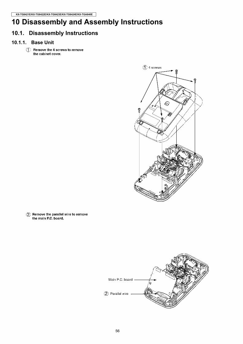
10 Disassembly and Assembly Instructions10.1. Disassembly Instructions10.1.1. Base Unit

57
KX-TG8421E/KX-TG8422E/KX-TG8423E/KX-TG8424E/KX-TGA840E

58
KX-TG8421E/KX-TG8422E/KX-TG8423E/KX-TG8424E/KX-TGA840E
10.1.2. Handset

59
KX-TG8421E/KX-TG8422E/KX-TG8423E/KX-TG8424E/KX-TGA840E
10.1.3. Charger Unit

60
KX-TG8421E/KX-TG8422E/KX-TG8423E/KX-TG8424E/KX-TGA840E
10.2. How to Replace the Handset LCD

61
KX-TG8421E/KX-TG8422E/KX-TG8423E/KX-TG8424E/KX-TGA840E
11 Measurements and Adjustments11.1. The Setting Method of JIG (Base Unit)11.1.1. Preparation11.1.1.1. Equipment Required
• DECT tester: Rohde & Schwarz, CMD 60 is recommended.• Frequency counter: It must be precise enough to measure intervals of 1 Hz (precision; ±4 ppm).
Hewlett Packard, 53131A is recommended.• Digital multi-meter (DMM): it must be able to measure voltage and current.• Oscilloscope
11.1.1.2. JIG and PC• Serial JIG
JIG Cable: PQZZ1CD300E*• PC which runs in DOS mode• Batch file CD-ROM for setting: PNZZTG8421E
Note:*: If you have the JIG Cable for TCD500 series(PQZZ1CD505E), change the following values of resis-tance. Then you can use it as a JIG Cable for both TCD300and TCD500 series. (It is an upper compatible JIG Cable.)
11.1.2. PC Setting11.1.2.1. Connections
Connect the AC adaptor to DC-JACK (base unit). Connect the JIG Cable GND (black) to GND. Connect the JIG Cable RX (red) to URX and TX (yellow) to UTX.
Note:*: COM port names may vary depending on what your PC calls it.
Resistor Old value (kΩ) New value (kΩ)R2 22 3.3R3 22 3.3R4 22 4.7R7 4.7 10

62
KX-TG8421E/KX-TG8422E/KX-TG8423E/KX-TG8424E/KX-TGA840E
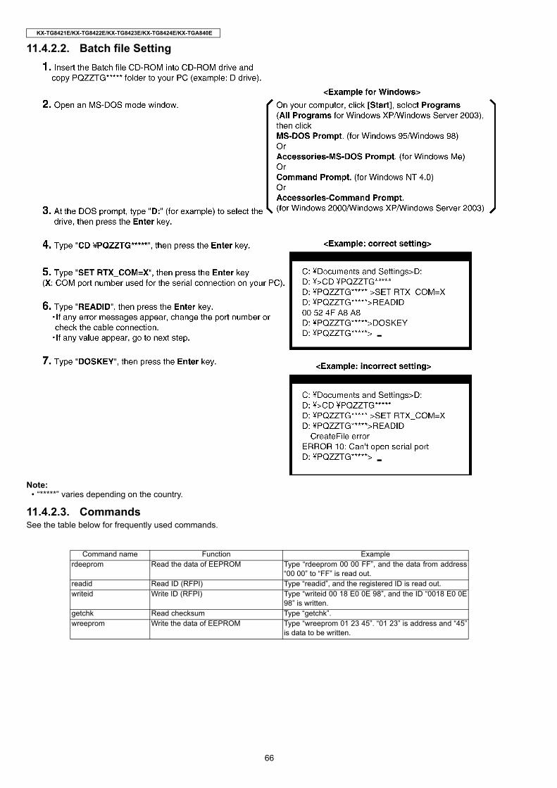
11.1.2.2. Batch file Setting
Note:• “****” varies depending on the country.
11.1.2.3. CommandsSee the table below for frequently used commands.
Command name Function Examplerdeeprom Read the data of EEPROM Type “rdeeprom 00 00 FF”, and the data from address
“00 00” to “FF” is read out.readid Read ID (RFPI) Type “readid”, and the registered ID is read out.writeid Write ID (RFPI) Type “writeid 00 18 E0 0E 98”, and the ID “0018 E0 0E
98” is written.hookoff Off-hook mode on Base Type “hookoff”.hookon On-hook mode on Base Type “hookon”.getchk Read checksum Type “getchk”.wreeprom Write the data of EEPROM Type “wreeprom 01 23 45”. “01 23” is address and “45”
is data to be written.

63
KX-TG8421E/KX-TG8422E/KX-TG8423E/KX-TG8424E/KX-TGA840E
11.2. Adjustment Standard (Base Unit)When connecting the simulator equipments for checking, please refer to below.
11.2.1. Bottom View
Note:(A) - (T) is referred to Check Point (Base Unit) (P.48)
A
PN
LB11
00Z
CH
G
SP
L2TL1T
L1RL2R
1
80
EE
E
1
CLK
VD
D5
VD
D4
VD
D3
VD
D2
UT
X
J101
RE
DW
HT
RE
DB
LK
GN
D
AN
T1_
TP
CL1
JTA
G
UR
X
4
E
DC
PbF
C421
C422C631
C625
C72
C137 C53C55
C54
C148
C423C84
C147
C826
C820
C305
C65C614
C61
VDD1
C617
C814
R76
R77R78
R75
R34
R81
R33
R37R36
R615
IC7SPp
DCP
DCM
SPm
Q421
Q9
AN
T2_
TP
CL2
C62
3C
626
C15
5
LIN
E_D
C
C18
C22 C
56
C16
7
C14
1
C24
C23
C85
7
C85
6
C85
5
C52
C16
9C
170
C13
6
C17
1
C16
8
C14
9 C74
C83
7C
75
C14
5C
146 C15
0
C85
8
R20
R23
R18R
24R
116
R12
R13
R35
R32
R87
R86
L2R
L1R
L2T
L1T
BLK
YLW
RE
DG
RN
TP
10
D23
D26
D21
Q2
C622
C14
C57
R19
R117
R29
R2
TP9
D22
D16
D15
Q5
GN
D_C
Q8
C61
5
C43
0
C60
C63
0
C61
6
R42
4R
425
R43
0
R42
6 R42
9
R42
8R
427
IC42
1
TP
16-s
ub
TP
16
TP
15-s
ub
TP
15
RA
80
RA
1
GND
LINE_DC
GND
CHARGE+
CHARGE-
GND
RX
TX
L1T(Q
)
(Q)
(I)
(Q)
((A
),(B
),(C
),(D
),(T
)
(R)
(G)
DT
MF
Tes
ter
CA
LL-I
DS
imul
ator
BE
LLS
imul
ator
AF
OS
C
AF
Vol
t M
eter
LOO
PS
imul
ator
OS
C
600
150
SP
DC
_IN
GN
DA
F V
olt
Met
er
Dum
my
Han
dset
AF
OS
C
6.3 V 47 F
CLK
GN
D
GN
D
(E),
(F),
(G),
(H)
(I)
,(J)
,(K
),(S
)(J
),(K
),(L
),(M
) (
N),
(O),
(P)
AN
T
CP
_2.5
V
+3.
0V
+2.
4V
+1.
8V
VD
D5
CP
_3.0
VV
DD
4
VD
D3
VD
D2
VD
D1
Fre
quen
cyC
ount
er
Dig
ital
Vol
t Met
er
Dig
ital
Vol
t Met
er
Dig
ital
Vol
t Met
erD
C P
OW
ER
DC
6.5
VD
EC
T T
este
rC
TS
60P
C
U-A
RT
L1R
50T
erm
inal
12 2W
OS
C
64
KX-TG8421E/KX-TG8422E/KX-TG8423E/KX-TG8424E/KX-TGA840E
11.3. Adjustment Standard (Charger Unit)When connecting the simulator equipment for checking, please refer to below.
11.3.1. Bottom View
Note:(A) is referred to Check Point (Charger Unit) (P.51)
TP
4
TP
3
1
2
J1
D1
AF
1Pb
FP
QLV
30055P
QLV
30056
PQ
UP
11532Z
Charge-
Charge+
10 /2 W
DigitalVolt Meter
(A)
DC POWERDC 6.5 V
TP
3
TP
4 (GN
D)

65
KX-TG8421E/KX-TG8422E/KX-TG8423E/KX-TG8424E/KX-TGA840E
11.4. The Setting Method of JIG (Handset)11.4.1. Preparation11.4.1.1. Equipment Required
• DECT tester: Rohde & Schwarz, CMD 60 is recommended.• Frequency counter: It must be precise enough to measure intervals of 1 Hz (precision; ±4 ppm).
Hewlett Packard, 53131A is recommended.• DC power: it must be able to output at least 1 A current under 2.4 V for Handset.• Digital multi-meter (DMM): it must be able to measure voltage and current.• Oscilloscope
11.4.1.2. JIG and PC• Serial JIG
JIG Cable: PQZZ1CD300E*• PC which runs in DOS mode.• Batch file CD-ROM for setting: PNZZTG8421E
Note:*: If you have the JIG Cable for TCD500 series(PQZZ1CD505E), change the following values of resis-tance. Then you can use it as a JIG Cable for both TCD300and TCD500 series. (It is an upper compatible JIG Cable.)
11.4.2. PC Setting11.4.2.1. Connections
Connect the DC Power or Battery to BATT+ and BATT-.
Connect the JIG cable GND (black) to GND.
Connect the JIG cable UTX (yellow) to UTX and URX (red) to URX.
Note:*: Com port names may vary depending on what your PC calls it.
Resistor Old value (kΩ) New value (kΩ)R2 22 3.3R3 22 3.3R4 22 4.7R7 4.7 10
66
KX-TG8421E/KX-TG8422E/KX-TG8423E/KX-TG8424E/KX-TGA840E
11.4.2.2. Batch file Setting
Note:• “*****” varies depending on the country.
11.4.2.3. CommandsSee the table below for frequently used commands.
Command name Function Examplerdeeprom Read the data of EEPROM Type “rdeeprom 00 00 FF”, and the data from address
“00 00” to “FF” is read out.readid Read ID (RFPI) Type “readid”, and the registered ID is read out.writeid Write ID (RFPI) Type “writeid 00 18 E0 0E 98”, and the ID “0018 E0 0E
98” is written.getchk Read checksum Type “getchk”.wreeprom Write the data of EEPROM Type “wreeprom 01 23 45”. “01 23” is address and “45”
is data to be written.

67
KX-TG8421E/KX-TG8422E/KX-TG8423E/KX-TG8424E/KX-TGA840E
11.5. Adjustment Standard (Handset)When connecting the simulator equipments for checking, please refer to below.
11.5.1. Component View
Note:(A) - (R) is referred to Check Point (Handset) (P.52)
A
PbF
PNLB1104ZKX-TGA840XX EU
C138
C71 C152 C70
RECEIVER
C139
SPEAKER
C29
C802C72
C813C811 C804
C73
C147
C121
C5
C3
F1
C76C77
C113
C54C40
C44 C834
C814C863C864
C43
C47
C83
C185
C35
C39
C110
4
5
1
X_CLK
POWER
1.8V
C128
C2
C1
C172
CP4.0V
CP2.5V
C111
C33
C6
C7
C837
C14C13
C38C332
C51C55
C53
C52
C49
R71
R209R208
R63R66
R64R225
R802
R805
R6
R74 R73 R31
R7
R30R4 R8
R45
R300R303R301R302R305
R12
R42R41R40
R32
R33 R25
R203
R807
R22
R28
R332
R330
R331
R306R304
R20
R307
L804
L802
L3
L9
L72
L73
L74L71
IC1
TEST
JTAG
RA61
BATT- BATT+
RA4
D21
D22
D14D13
BLK
REDB
LK
RE
D
D8
D7
D4 D3
Q4
Q7
Q11
Q12
Q2
C4
5
C3
6
C4
6 C8
60
C1
82
C8
19
C8
25
C8
27C
80
9C
81
0C
80
5
C808
C8
61
C8
12
C8
59
C8
62
C8
03
C8
06
CN
4
C7
4
C7
5
C4
C1
5
C1
50
C1
88
C9
7 C9
6
C8
22
C8
26
C4
1
X1
C8
20
C1
8 C1
1 C1
0C
12
C1
6
C3
31
C1
84
C1
7
C4
8
C5
0
C1
09
C8
2
32
11
4
85
1
C1
08
C8
6C1
27
R6
5
R8
08
R8
01
R8
06
R8
03
R8
04SP-PHO
NE_SPEAKER
R3
10
R3
09
R2
R2
15
R2
7
R1
52
R3
4
R3
08
R1
00
L8
01
L8
03
L5
L4
L8
IC801
IC3
RA
1
RA
2
DA
80
1D
1Q
9
UTX URX
GND
CHG (-)
CH
G (+
)
BAT
MIC- MIC+
OS
C
AF
VO
LTM
ET
ER
LO
OP
Sim
ula
tor
Du
mm
y B
ase
Un
it
6.3
V 4
7
F
6.3
V 4
7
F
AF
GE
NE
RAT
OR
DC
6.5
V
DC
PO
WE
R2
.30
-2.6
0V
DC
PO
WE
R2
.00
-2.2
5V
GN
D
Dig
ital
Vo
lt M
ete
rU
TX
UR
XG
ND
PC
GN
D
CL
K
Fre
qu
en
cyC
ou
nte
r
2.7
VZ
en
er
AF
OS
C
MIC
-
(D),
(E),
(F),
(G)
(A),
(B),
(C),
(F),
(G),
(H),
(I)
(A
),(Q
),(R
)
iH)
(I),
(J),
(K),
(L),
(M),
(N)
(O),
(P)
(O)
(O
),(P
)
MIC
++
+
60
0
10
0
GN
DA
NT D
EC
T T
est
er
CM
D6
0
(at
ba
tte
ry lo
w)
PO
WE
R K
EY
15
0
56
56
SP+REV-
REV+
SP-
8 1
F
AF
VO
LTM
ET
ER
Osc
illo
sco
pe
AB1
22
pF
Cu
rre
nt
Pro
be
Osc
illo
sco
pe
1.8
V
CP
2.5
V
CP
4.0
V

68
KX-TG8421E/KX-TG8422E/KX-TG8423E/KX-TG8424E/KX-TGA840E
11.6. Things to Do after Replacing IC or X'talCautions:
Some of the content on this page may not apply to models from some countries.
11.6.1. Base UnitBefore making the following adjustment, ensure you have carried out PC Setting (P.61) in The Setting Method of JIG (BaseUnit).
Note:(*1) XX: country code, YY: revision number, ZZ: Voice Prompt“XX”, “YY” and “ZZ” vary depending on the country version. You can find them in the batch file, PQZZ- mentioned in JIG and PC(P.61).(*2) Refer to Check Point (Base Unit) (P.48)
Items Necessary AdjustmentBBIC (FLASH type)(IC7)
Programs for Voice processing, interface for RFand EEPROM
1. Make sure to connect the JIG cable, then detach the DCPower.
2. Execute the command “flw480 *********.hex”.3. Connect the DC Power.4. Press the PC Enter key once.5. After a few minutes, “Successful upgrade” is displayed
on the PC indicating downloading has finished.6. Detach the JIG cable, then disconnect the DC Power.7. Connect the DC Power.8. Connect the JIG cable again, and execute the command
“getchk”, then confirm the checksum value is correct.• If the downloading fails, start again from step 1.
9. Default batch file: Execute the command “default.bat”.10. Country version batch file: Execute the command
“TG8421XXrevYY.bat”. (*1)11. Clock adjustment: Refer to Check Point (G). (*2)
EEPROM (IC401) Adjustment parameter data(country version batch file, default batch file,etc.)
1. Change the address “0000” of EEPROM to “AA”.2. Default batch file: Execute the command “default.bat”.3. Country version batch file: Execute the command
“TG8421XXrevYY.bat”. (*1)4. Clock adjustment: Refer to Check Point (F). (*2)
FLASH (IC421) Voice prompt data(vary depending on country version)
1. Wait more than 15 seconds after connecting the JIGCable
2. Execute the command "VPDL2009 -57600 ZZ.bin"(*1)(writing time: aprox. About 1 min (57600bps).)
X'tal (X1) System clock 1. Refer to Check Point (F). (*2)

69
KX-TG8421E/KX-TG8422E/KX-TG8423E/KX-TG8424E/KX-TGA840E
11.6.2. HandsetBefore making the following adjustment, ensure you have carried out PC Setting (P.65) in The Setting Method of JIG (Hand-set).
Note:(*3) XX: country code, YY: revision number“XX” and “YY” vary depending on the country version. You can find them in the batch file, PQZZ- mentioned in JIG and PC(P.61).
(*4) Refer to Check Point (Handset) (P.52)
Items Necessary AdjustmentBBIC (FLASH type)(IC1)
Programs for Voice processing, interface for RFand EEPROM
1. Make sure to connect the JIG cable, then detach the DCPower.
2. Execute the command “flw480 *********.hex”.3. Connect the DC Power.4. Press and hold the handset Power key.5. While holding down the handset Power key, press the PC
Enter key once.6. After a few minutes, “Successful upgrade” is displayed
on the PC indicating downloading has finished.7. Detach the JIG cable, then press the handset Power key
to turn it on.8. Connect the JIG cable again, and execute the command
"getchk”, then confirm the checksum value is correct.• If the downloading fails, start again from step 1.
9. Default batch file: Execute the command “default.bat”.10. Default batch file (remaining): Execute the Command
“TGA840DEFrevYY.bat”. (*3).11. Country version batch file: Execute the command
“TGA840XXrevYY.bat”. (*3).12. Clock adjustment: Refer to Check Point (H). (*4).13. 1.8 V setting and battery low detection: Refer to Check
Point (A), (F) and (G). (*4).EEPROM (IC3) Adjustment parameter data
(country version batch file, default batch file,etc.)
1. Default batch file: Execute the command “default.bat”.2. Default batch file (remaining): Execute the Command
“TGA840DEFrevYY.bat”. (*3)3. Country version batch file: Execute the command
“TGA840XXrevYY.bat”. (*3)4. Clock adjustment: Refer to Check Point (J). (*4)5. 1.8 V setting and battery low detection: Refer to Check
Point (A), (F) and (G). (*4)X'tal (X1) System clock 1. Refer to Check Point (H). (*4)
70
KX-TG8421E/KX-TG8422E/KX-TG8423E/KX-TG8424E/KX-TGA840E
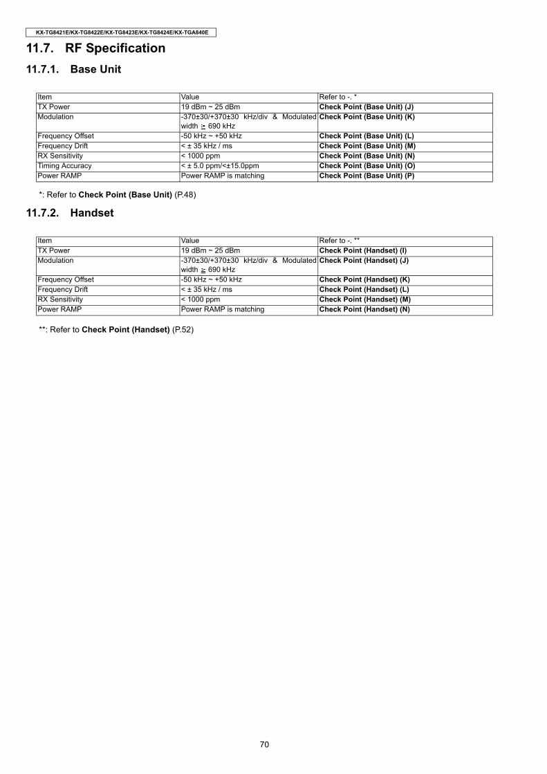
11.7. RF Specification11.7.1. Base Unit
*: Refer to Check Point (Base Unit) (P.48)
11.7.2. Handset
**: Refer to Check Point (Handset) (P.52)
Item Value Refer to -. *TX Power 19 dBm ~ 25 dBm Check Point (Base Unit) (J)Modulation -370±30/+370±30 kHz/div & Modulated
width 690 kHzCheck Point (Base Unit) (K)
Frequency Offset -50 kHz ~ +50 kHz Check Point (Base Unit) (L)Frequency Drift < ± 35 kHz / ms Check Point (Base Unit) (M)RX Sensitivity < 1000 ppm Check Point (Base Unit) (N)Timing Accuracy < ± 5.0 ppm/<±15.0ppm Check Point (Base Unit) (O)Power RAMP Power RAMP is matching Check Point (Base Unit) (P)
Item Value Refer to -. **TX Power 19 dBm ~ 25 dBm Check Point (Handset) (I)Modulation -370±30/+370±30 kHz/div & Modulated
width 690 kHzCheck Point (Handset) (J)
Frequency Offset -50 kHz ~ +50 kHz Check Point (Handset) (K)Frequency Drift < ± 35 kHz / ms Check Point (Handset) (L)RX Sensitivity < 1000 ppm Check Point (Handset) (M)Power RAMP Power RAMP is matching Check Point (Handset) (N)

71
KX-TG8421E/KX-TG8422E/KX-TG8423E/KX-TG8424E/KX-TGA840E
11.8. How to Check the Handset Speaker or Receiver1. Prepare the digital voltmeter, and set the selector knob to ohm meter.2. Put the probes at the speaker terminals as shown below.
11.9. Frequency Table (MHz)
Note:Channel No. 10: In the Test Mode on Base Unit and Handset.
BASE UNIT HANDSETChannel No Transmit Frequency Receive Frequency Transmit Frequency Receive Frequency1 1897.344 1897.344 1897.344 1897.344 2 1895.616 1895.616 1895.616 1895.616 3 1893.888 1893.888 1893.888 1893.888 4 1892.160 1892.160 1892.160 1892.160 5 1890.432 1890.432 1890.432 1890.432 6 1888.704 1888.704 1888.704 1888.704 7 1886.976 1886.976 1886.976 1886.976 8 1885.248 1885.248 1885.248 1885.2489 1883.520 1883.520 1883.520 1883.520 10 1881.792 1881.792 1881.792 1881.792

72
KX-TG8421E/KX-TG8422E/KX-TG8423E/KX-TG8424E/KX-TGA840E
12 Miscellaneous12.1. CPU Data (Base Unit)12.1.1. IC7 (BBIC)
Pin No. Description I/O Connection at Normal mode at Reset mode1 VSS_LNA1 - GND - -2 RF_RXp A.I RF_RXp A.I A.I3 RF_RXn A.I RF_RXn A.I A.I4 VSS_LNA2 - GND - -5 RFP1 D.O RXON O_0/1 Hi-Z6 RFP0 D.O ANT1 O_0/1 Hi-Z7 REF_RES A.O REF_RES A.O A.O8 AVS_XTAL - GND - -9 XTAL2 A.I XTAL2 A.I A.I
10 XTAL1 A.I XTAL1 A.I A.I11 AVD_XTAL - AVD_XTAL - -12 RF_SUPPLY1 - RF_SUPPLY1 - -13 LDO_CTRL A.O LDO_CTRL A.O O-114 AVD - AVD - -15 LSRn A.O LSRn A.O A.O16 LSRp A.O LSRp A.O A.O17 VREFm - VREFm - -18 MICh A.I MICh A.I A.I19 CIDOUT/MICn A.O CIDOUT A.O A.O20 CIDINn/MICp A.I CIDINn A.I A.I21 CIDINp/VREFp A.I CIDINp A.I A.I22 RINGp/P3_7 D.O N.C. O_0 O23 RINGn/P3_6 D.O HOOK O_0/1 O24 RINGOUT/RINGING/
P3_5A.O RINGING A.I A.I
25 PARADET/P3_4 A.I PARADET A.I A.I26 ADC0/P3_3 A.I ADC0 A.I A.I27 ADC1/INT0/P1_0 A.I ADC1 A.I A.I28 NTC/ADC2 - GND - A.I29 SOCp - GND - A.I30 SOCn - GND - A.I31 CHARGE_CTRL A.O N.C. A.O O-032 P1_7/CHARGE A.I CHARGE I I33 PAOUTp/P3_1 A.O PAOUTp A.O O-034 VDDPA - VDDPA - -35 PAOUTn/P3_0 A.O PAOUTn A.O O-036 VBAT1 - VBAT1 - -37 CP_C1x A.I/O N.C. A.I/O A.I38 CP_C2x A.I/O CP_C2x A.I/O A.I39 CP_C1y A.I/O N.C. A.I/O A.I40 VBAT2 - VBAT2 - -41 CP_C2y A.I/O CP_C2y A.I/O A.I42 CP_VOUT1/LED1 A.O CP_VOUT1 A.O A.O43 CP_VOUT2/LED2 A.O CP_VOUT2 A.O A.O44 PON/P1_6 D.I PullUp I_1 I45 VDD1 - +1.8V - -46 P2_7/BXTAL D.O TAM_WP O_0/1 O-147 P1_5/INT5/RDI/VDDE D.I ROW2 I_0/1 I-PU48 P1_4/INT4/TDOD D.I ROW1 I_0/1 I-PU49 P1_3/INT3/SIO D.I ROW0 I_0/1 I-PU50 P1_2/INT2/SK D.O KEY1 O_0/1 O-051 P1_1/INT1/LE D.O KEY0 O_0/1 O-052 P2_6/WTF_IN D.O KEY2 O_0/1 O-053 P0_7/SPI_DI D.I SPI_DI I_0/1 I-PU54 P0_6/SPI_DO D.O SPI_DO O_0/HighZ O-055 P0_5/SPI_CLK D.O SPI_CLK O_0/HighZ O-056 P0_4/SPI_EN D.O TAM_CSn O_0/HighZ O-157 P0_3/SCL2 D.O SCL2 O_0/HighZ O-058 P0_2/SDA2 D.I/O SDA2 I/O_0/HighZ O-0
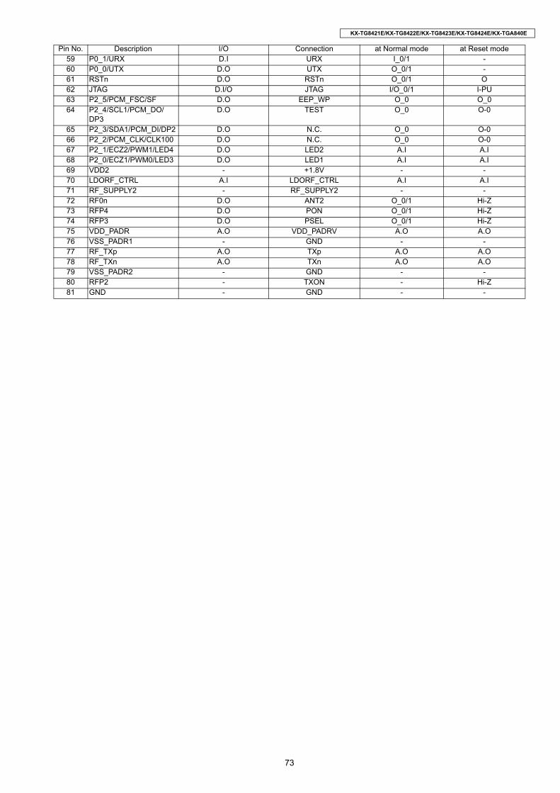
73
KX-TG8421E/KX-TG8422E/KX-TG8423E/KX-TG8424E/KX-TGA840E
59 P0_1/URX D.I URX I_0/1 -60 P0_0/UTX D.O UTX O_0/1 -61 RSTn D.O RSTn O_0/1 O62 JTAG D.I/O JTAG I/O_0/1 I-PU63 P2_5/PCM_FSC/SF D.O EEP_WP O_0 O_064 P2_4/SCL1/PCM_DO/
DP3D.O TEST O_0 O-0
65 P2_3/SDA1/PCM_DI/DP2 D.O N.C. O_0 O-066 P2_2/PCM_CLK/CLK100 D.O N.C. O_0 O-067 P2_1/ECZ2/PWM1/LED4 D.O LED2 A.I A.I68 P2_0/ECZ1/PWM0/LED3 D.O LED1 A.I A.I69 VDD2 - +1.8V - -70 LDORF_CTRL A.I LDORF_CTRL A.I A.I71 RF_SUPPLY2 - RF_SUPPLY2 - -72 RF0n D.O ANT2 O_0/1 Hi-Z73 RFP4 D.O PON O_0/1 Hi-Z74 RFP3 D.O PSEL O_0/1 Hi-Z75 VDD_PADR A.O VDD_PADRV A.O A.O76 VSS_PADR1 - GND - -77 RF_TXp A.O TXp A.O A.O78 RF_TXn A.O TXn A.O A.O79 VSS_PADR2 - GND - -80 RFP2 - TXON - Hi-Z81 GND - GND - -
Pin No. Description I/O Connection at Normal mode at Reset mode

74
KX-TG8421E/KX-TG8422E/KX-TG8423E/KX-TG8424E/KX-TGA840E
12.2. CPU Data (Handset)12.2.1. IC1 (BBIC)
Pin No. Description I/O Connection at Normal mode at Reset mode1 VSS_LNA1 - GND - -2 RF_RXp A.I RF_RXp A.I A.I3 RF_RXn A.I RF_RXn A.I A.I4 VSS_LNA2 - GND - -5 RFP1 D.O RXON O_0/1 L6 RFP0 D.O ANT1 O_0/1 L7 REF_RES A.O REF_RES A.O A.O8 AVS_XTAL - GND - -9 XTAL2 A.I XTAL2 A.I A.I
10 XTAL1 A.I XTAL1 A.I A.I11 AVD_XTAL - AVD_XTAL - -12 RF_SUPPLY1 - RF_SUPPLY1 - -13 LDO_CTRL A.O LDO_CTRL A.O H14 AVD - +1.8V - -15 LSRn A.O LSRn A.O A.O16 LSRp A.O LSRp A.O A.O17 VREFm - GND - -18 MICh A.I MICh A.I A.I19 CIDOUT/MICn A.I MICn A.I A.I20 CIDINn/MICp A.I MICp A.I A.I21 CIDINp/VREFp A.O VREFp A.O -22 RINGp/P3_7 D.O COL4 O_0/1 L23 RINGn/P3_6 D.O COL3 O_0/1 L24 RINGOUT/RINGING/
P3_5D.O COL2 O_0/1 L
25 PARADET/P3_4 D.O COL1 O_0/1 L26 ADC0/P3_3 D.O COL0 O_0/1 L27 ADC1/INT0/P1_0 - N.C. - L28 NTC/ADC2 A.I ADC2 A.I A.I29 SOCp A.I SOCp A.I A.I30 SOCn A.I SOCn A.I A.I31 CHARGE_CTRL A.O CHARGE_CTRL A.O A.O32 P1_7/CHARGE A.I CHARGE A.I I-PD33 PAOUTp/P3_1 A.O PAOUTp A.O L34 VDDPA - VDDPA - -35 PAOUTn/P3_0 A.O PAOUTn A.O L36 VBAT1 - VBAT1 - -37 CP_C1x A.O CP_C1x A.O A.O38 CP_C2x A.O CP_C2x A.O A.O39 CP_C1y A.O CP_C1y A.O A.O40 VBAT2 - VBAT2 - -41 CP_C2y A.O CP_C2y A.O A.O42 CP_VOUT1/LED1 A.O CP_VOUT1 A.O A.O43 CP_VOUT2/LED2 A.O CP_VOUT2 A.O A.O44 PON/P1_6 A.I PON A.I L45 VDD1 - +1.8V - -46 P2_7/BXTAL D.O COL5 D.O L47 P1_5/INT5/RDI/VDDE - N.C. - L48 P1_4/INT4/TDOD D.I ROW0 D.I I-PD49 P1_3/INT3/SIO D.I ROW3 D.I I-PD50 P1_2/INT2/SK D.I ROW2 D.I I-PU51 P1_1/INT1/LE D.I ROW1 D.I I-PU52 P2_6/WTF_IN D.O KEY_LED D.O L53 P0_7/SPI_DI D.O EEPROM_WP D.O I-PU54 P0_6/SPI_DO D.O LCD_SDA D.O L55 P0_5/SPI_CLK D.O LCD_SCL D.O L56 P0_4/SPI_EN D.O LCD_CD D.O L57 P0_3/SCL2 D.O SCL D.O L58 P0_2/SDA2 D.I/O SDA D.I/O L59 P0_1/URX D.I URX D.I I-PU60 P0_0/UTX D.O UTX D.O L61 RSTn D.O RSTn D.O I-PU
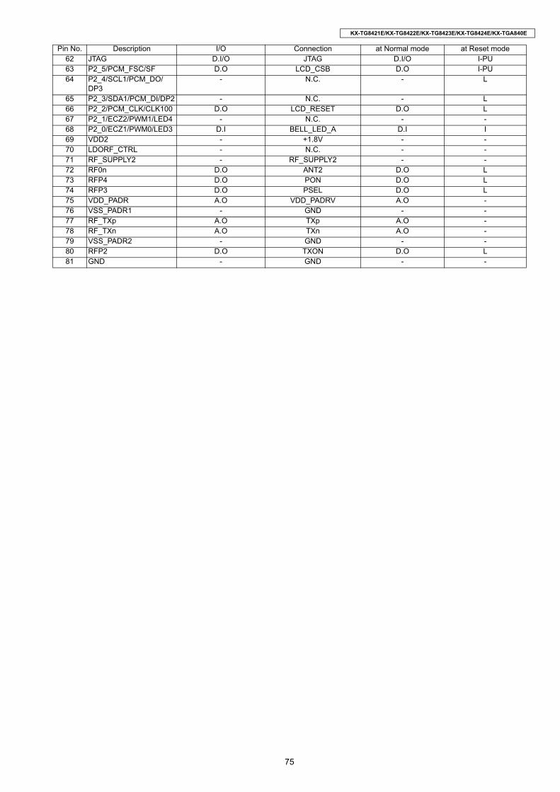
75
KX-TG8421E/KX-TG8422E/KX-TG8423E/KX-TG8424E/KX-TGA840E
62 JTAG D.I/O JTAG D.I/O I-PU63 P2_5/PCM_FSC/SF D.O LCD_CSB D.O I-PU64 P2_4/SCL1/PCM_DO/
DP3- N.C. - L
65 P2_3/SDA1/PCM_DI/DP2 - N.C. - L66 P2_2/PCM_CLK/CLK100 D.O LCD_RESET D.O L67 P2_1/ECZ2/PWM1/LED4 - N.C. - -68 P2_0/ECZ1/PWM0/LED3 D.I BELL_LED_A D.I I69 VDD2 - +1.8V - -70 LDORF_CTRL - N.C. - -71 RF_SUPPLY2 - RF_SUPPLY2 - -72 RF0n D.O ANT2 D.O L73 RFP4 D.O PON D.O L74 RFP3 D.O PSEL D.O L75 VDD_PADR A.O VDD_PADRV A.O -76 VSS_PADR1 - GND - -77 RF_TXp A.O TXp A.O -78 RF_TXn A.O TXn A.O -79 VSS_PADR2 - GND - -80 RFP2 D.O TXON D.O L81 GND - GND - -
Pin No. Description I/O Connection at Normal mode at Reset mode
76
KX-TG8421E/KX-TG8422E/KX-TG8423E/KX-TG8424E/KX-TGA840E
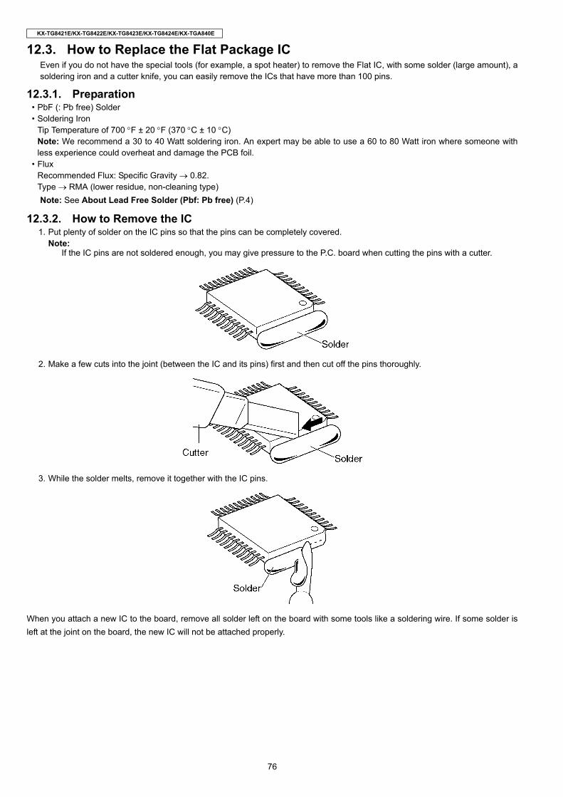
12.3. How to Replace the Flat Package ICEven if you do not have the special tools (for example, a spot heater) to remove the Flat IC, with some solder (large amount), asoldering iron and a cutter knife, you can easily remove the ICs that have more than 100 pins.
12.3.1. Preparation• PbF (: Pb free) Solder• Soldering Iron
Tip Temperature of 700 °F ± 20 °F (370 °C ± 10 °C)Note: We recommend a 30 to 40 Watt soldering iron. An expert may be able to use a 60 to 80 Watt iron where someone withless experience could overheat and damage the PCB foil.
• FluxRecommended Flux: Specific Gravity → 0.82.Type → RMA (lower residue, non-cleaning type)Note: See About Lead Free Solder (Pbf: Pb free) (P.4)
12.3.2. How to Remove the IC1. Put plenty of solder on the IC pins so that the pins can be completely covered.
Note:If the IC pins are not soldered enough, you may give pressure to the P.C. board when cutting the pins with a cutter.
2. Make a few cuts into the joint (between the IC and its pins) first and then cut off the pins thoroughly.
3. While the solder melts, remove it together with the IC pins.
When you attach a new IC to the board, remove all solder left on the board with some tools like a soldering wire. If some solder isleft at the joint on the board, the new IC will not be attached properly.

77
KX-TG8421E/KX-TG8422E/KX-TG8423E/KX-TG8424E/KX-TGA840E
12.3.3. How to Install the IC1. Temporarily fix the FLAT PACKAGE IC, soldering the two marked pins.
*Check the accuracy of the IC setting with the corresponding soldering foil.
2. Apply flux to all pins of the FLAT PACKAGE IC.
3. Solder the pins, sliding the soldering iron in the direction of the arrow.
12.3.4. How to Remove a Solder Bridge1. Lightly resolder the bridged portion.2. Remove the remaining solder along the pins using a soldering iron as shown in the figure below.

78
KX-TG8421E/KX-TG8422E/KX-TG8423E/KX-TG8424E/KX-TGA840E
12.4. How to Replace the LLP (Leadless Leadframe Package) IC12.4.1. Preparation
• PbF (: Pb free) Solder• Soldering Iron
Tip Temperature of 700°F ± 20°F (370°C ± 10°C)Note:We recommend a 30 to 40 Watt soldering iron. An expert may be able to use a 60 to 80 Watt iron where someone with less experience could overheat and damage the PCB foil.
• Hot Air Desoldering ToolTemperature: 608°F ± 68°F (320°C ± 20°C)
12.4.2. Caution• To replace the IC efficiently, choose the right sized nozzle of the hot air desoldering tool that matches the IC package.• Be careful about the temperature of the hot air desoldering tool not to damage the PCB and/or IC.
12.4.3. How to Remove the Shield CaseNote:
If you don’t have special tools (ex. Hot air disordering tool), conduct the following operations.
1. Cut the case along perforation.
2. Remove the cut part.
3. Cut the four corners along perforation.
4. Remove the reminds by melting solder.
12.4.4. How to Install the Shield CaseNote:
• If you don’t have special tools (ex. Hot air disordering tool), conduct the following operations.• Shield case’s No. : PNMC1013Z

79
KX-TG8421E/KX-TG8422E/KX-TG8423E/KX-TG8424E/KX-TGA840E
1. Put the shield case.
2. Solder the surroundings.
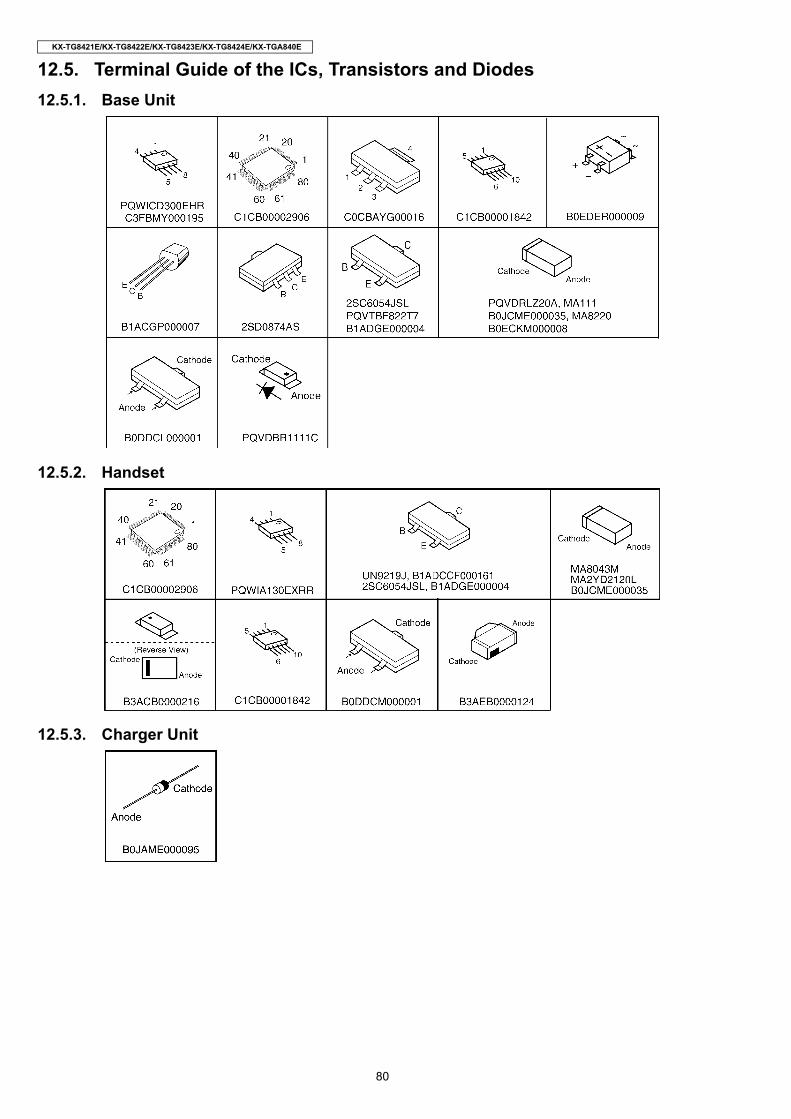
80
KX-TG8421E/KX-TG8422E/KX-TG8423E/KX-TG8424E/KX-TGA840E
12.5. Terminal Guide of the ICs, Transistors and Diodes12.5.1. Base Unit
12.5.2. Handset
12.5.3. Charger Unit

81
KX-TG8421E/KX-TG8422E/KX-TG8423E/KX-TG8424E/KX-TGA840E
Memo
82
KX-TG8421E/KX-TG8422E/KX-TG8423E/KX-TG8424E/KX-TGA840E
13 Schematic Diagram13.1. For Schematic Diagram13.1.1. Base Unit (Schematic Diagram (Base Unit))Notes:
1. DC voltage measurements are taken with voltmeter from the negative voltage line.
2. The schematic diagrams may be modified at any time with the development of new technology.
13.1.2. Handset (Schematic Diagram (Handset))Notes:
1. DC voltage measurements are taken with an oscilloscope or a tester with a ground.2. The schematic diagram may be modified at any time with the development of new technology.
13.1.3. Charger Unit (Schematic Diagram (Charger Unit))Notes:
1. DC voltage measurements are taken with voltmeter from the negative voltage line.
2. The schematic diagram may be modified at any time with the development of new technology.

83
KX-TG8421E/KX-TG8422E/KX-TG8423E/KX-TG8424E/KX-TGA840E
Memo:

84
KX-TG8421E/KX-TG8422E/KX-TG8423E/KX-TG8424E/KX-TGA840E
13.2. Schematic Diagram (Base Unit)
3.0V
2.5V
TX _RF
TX _RF
RX _RF
BeepBell signal
GND
SPm
SPp
GND GND
GND
*C50
5N
C
*C50
2N
C
*SW1
NC
12
GND
NC
*C501
GND
+3.0V
100
R75
270k
*R425
UTX
URX
GND
ANT_1
AN
T2
NC
C85
4
AN
T1
GNDGND
ANT_2
GND
NC
C85
0
GND GND
0R511
0*R542
0*R516
0*RA501
1
2
3
4 5
6
7
8
1kR76
0*R532
ANT1_TPANT2_TP
GNDGND
GND
1uC61
6
GND
+3.0V
GND
AP1
*CN5 .
PARALLEL WIRE
GND
10k
R77R78
NC
GND
+2.5_CP
1uC62
5
*C50
3N
C
NC
C43
0
GND
CL1 CL2
GND
10p
C81
1
GND
100n
C80
8
GND
GND
GND
PON1k
R804
RF_RXp
RF_RXn
GND
GND
GND
TXp
GND
10p
C81
9
220
R806
GND
TXn
GND
PSEL
3.3n
C81
4
10p
C82
5
VDD_PADRV
TXON
1k
R803
GND
1PSET2VCCS3PI4PIX7 PSEL
8 POX
9 PO
10 VCC
11
GND
5PRAMP6 PAON
GND
GND
GND
RXON220
R807
10p
C80
9
GND
47R805
GND
10n
*C42
1
GNDGND
10k
*R424
NC*C423
GND
*Q421
VDD5
GND100n
*C422
560
*R42
6
560
*R42
7
560
*R42
8
3.3k
*R42
9GND
10k
*R13
5
GND
10R43
0
10p
C827
GND
GND
C85910p
10p
C85
5
10p
C85
7
100p
C85
6
100p
C85
8
10p
*C14
510
p
*C14
6
10p
C812
10p
C63
0
10p
C63
1
GND
GND
10100nC60
CLK
GN
D_C
*Q24NC
*C50
4N
C
GND
NC
C50
6
+1.8V
C83
7
NC
CN5-10
CN5-9
CN5-8
CN5-7
CN5-6
CN5-5
CN5-4
CN5-3
CN5-2
CN5-1
1.5p
C803
27n
L801
DA802
1 2
3
DA8011
23
10p
*C51
1
10p
*C51
2
10p
*C51
3
10p
*C51
4
10p
*C51
5
10p
*C51
6
C853
2p
1.8p
C80
4
1.8p
C80
2
Shi
eld
12
3
45
6
3nL802
3nL803
GND
C851
2p
10p
C82
2
3.3p
C80
5
3.3p
C80
6
2.2p
C81
0
2.2p
C81
3
VDD4
*C16
3
NC
10p
*C51
7
10p
*C51
8
10p
*C51
9
GND
C52
0
NC
GND
JTAG
3pC86
0
GND
10pC861
GND
1.5*R86
1.5*R87
220RA801
23
4
NC
*R13
2
2.2n
*C14
92.
2n
*C15
0
GNDGND
100p
C82
3
GND
0.9p
C826
0.75
p
C82
0
120
R80
2
0.5p
C83
4
1 *CE
2 SO
3 *WP
4 VSS 5SI
6SCK
7*HOLD
8VDD
1.5k
*R80
8
1.5k
*R80
1
SDA2SCL2TAM_CSnSPI_CLK
TAM_WP
KEY0KEY1
ROW1ROW2
KEY2
ROW0
LED1
CHARGE
TAM_WP
SPI_DISPI_DO
SPI_DO
TAM_CSn
SPI_DI
SPI_CLK
Low_Rad
LED2
ROW1
ROW2
KEY0
KEY1
KEY2
ROW0
RO
W0
for TG8421/6421
for TG6411/8411
CP_OUT1=3.0V
Pow_Adj
Pre-matching
Balun
BPF
W 0.15mmL 22+/-4mm1st or 4th layer
W 0.15mmL 22+/-4mm1st or 4th layer
W 0.15mmL 22+/-4mm1st or 4th layer
W 0.15mmL 5.0mm1st layer
W 0.15mmL 5.0mm1st layer
W 0.15mmL 20+/-2mm3rd layer
W 0.15mmL 20+/-2mm3rd layer
W 0.15mmL 20+/-1mm3rd layer
W 0.125mmL 7.6mmGap 0.125mm1st layer
W 0.15mmL 4.0mm x2 1st layer
IC801
*IC421
(1)
(2)
(3)(4)
(5)
(7)
(6)
(8)
(9)
NC: No Components

85
KX-TG8421E/KX-TG8422E/KX-TG8423E/KX-TG8424E/KX-TGA840E
1.8V 3.0V
TX _RF
RX _RF
TX _AF
Bell signalCaller ID
0.75V
0V
250mVp-p
Loop Current
Charge Current
RX_AF
Bell signal
GND
GND
Q8
1uC61
4
GND
+1.8V
GND
GN
D
GND
GND
56k FR615GND
GND
GND
SA
1
L1
L2
GND GND
J101
GND
GND
+8.0V
K2.
2u
C31
GND
4Fin
1ADJ/GND
3Input
2 Output
GND GND
GND
10k
R16 GND
GND
GND
GND
NC
(321
6)
R12
3
100k
R14
2.7k
R15
D3
4
1
3
2
GND GND
2.2kR17
GND
K2.
2u
*C16
27k
R18
GND
K2.
2u
C17
GND0.
1u
C28
100k
R27
K1u
C15
GND
TP10
100
R116
4700
p
C14
8.2k
R19
100k
R23
+1.8V
NC
C18
GND
GND
GND
GND
GND
NC
C24
NC
C57
47k
R24
GND
GND
12R21
GND
TP9
K0.
22u
C23
470k
R28
K0.
1u
C56
K0.
22u
C14
1
GND
GND
1u
C22
(1005) NC
C155
1kR33
1kR35
GND
GND10p
C136
GND
100k
R10
GND
+1.8V
GND
GND
100k
R8
100n
C72
100nC61
GND
3.3kR
81
3.3k
R11
7
+1.8V1n
C15
7
TP16
TP15
NC
*C48
NC
*C15
6
GND
GND
GND
3.9
R55
GND
GND
100n
C51
GND
GND
GND
100nC
75
NC
*D16 A
K
D1A
K
Q4
D23
NC
*D15
AK
+3.0V2.2u
C84
C306 NC1u
C305
GND
GND
1k
R130 10k
R12
9
3AF1
*R2
NC
D21
10kRA402
1
23
4
*Q23NC
*D5 A
K
*D6
AK
D9
AK
1u
C615
Q9
+2.5V
+2.5V
GND
F 14
0
R39
F 10
0
R38
220R106
220R109
NCC2
GND
C16
7
NC
VDD2
100nC7
100nC8
10pC65
+2.5_CP
C62
3N
C
L2TL1TL1R
DC
M
DC
P
L2R
C12
NC
10p
C13
7
GNDC
166 NC
100u
16
C32
5010
u
C27
*C49
NC
GND
10.368MX11 3
2
120
R29
NC
D26
ANT1
RF_RXn
RXON
TXON
TXn
TXp
VDD_PADRV
PSEL
PON
ANT2
RF_RXp
GND
C62
6N
C
1033
0u
C36
10k
R65
7
GND
GND
GNDGND
Q5
Q3
10p*C148
10p*C147
10pC170
10pC169
10pC168
10pC74
680pC9
500
680p
C10 500
1kRA1
1 2 3 45678
*C62
2N
C
D22
LINE_DC
NC
*R126
HAK_CL1
3.9
R56
TEST
VDD3VDD1
NC
C1
10pC171
120k
R36
C61
71u 10
5pC29
5pC30
C37 5p
1MR4
1MR6
180k
R3
180k
R5
C5
10n
10n
C6
10n
C42
10n
C43
4.7M
R42
4.7M
R43
680pC3
680pC4
33nC54
C55
82n
1k
R37 82kR32
82k
R34
820pC52
820p
C53
GND
10p
C70
1VSS_LNA12RF_RXp
21C
IDIN
p/V
RE
Fp
3RF_RXn4VSS_LNA25RFP16RFP07REF_RES8AVS_XTAL
22R
ING
p/P
3_7
23R
ING
n/P
3_6
24R
ING
OU
T/R
ING
ING
/P3_
5
25PA
RA
DE
T/P
3_4
26A
DC
0/P
3_3
27A
DC
1/IN
T0/P
1_0
28N
TC/A
DC
2
41 CP_C2y
42 CP_VOUT1/LED1
43 CP_VOUT2/LED2
44 PON/P1_6
45 VDD1
46 P2_7/BXTAL
81
GN
D
9XTAL210XTAL111AVD_XTAL12RF_SUPPLY113LDO_CTRL14AVD15LSRn16LSRp17VREFm18MICh19CIDOUT/MICn20CIDINn/MICp
29S
OC
p
30S
OC
n
31C
HA
RG
E_C
TRL
32P
1_7/
CH
AR
GE
33PA
OU
Tp/P
3_1
34V
DD
PA
35PA
OU
Tn/P
3_0
36V
BAT
1
37C
P_C
1x
38C
P_C
2x
39C
P_C
1y
40V
BAT
2
47 P1_5/INT5/RDI/VDDE
48 P1_4/INT4/TDOD
49 P1_3/INT3/SIO
50 P1_2/INT2/SK
51 P1_1/INT1/LE
52 P2_6/WTF_IN
53 P0_7/SPI_DI
54 P0_6/SPI_DO
55 P0_5/SPI_CLK
56 P0_4/SPI_EN
57 P0_3/SCL2
58 P0_2/SDA2
59 P0_1/URX
60 P0_0/UTX
61R
STn
62JT
AG63
P2_
5/P
CM
_FS
C/S
F64
P2_
4/S
CL1
/PC
M_D
O/D
P3
65P
2_3/
SD
A1/
PC
M_D
I/DP
266
P2_
2/P
CM
_CLK
/CLK
100
67P
2_1/
EC
Z2/P
WM
1/LE
D4
68P
2_0/
EC
Z1/P
WM
0/LE
D3
69V
DD
270
LDO
RF_
CTR
L71
RF_
SU
PP
LY2
72R
FP0n
73R
FP4
76V
SS
_PA
DR
1
79V
SS
_PA
DR
2
77R
F_TX
p
80R
FP2
75V
DD
_PA
DR
78R
F_TX
n
74R
FP3
*Q22
NC
*C25
0.01
u
5.6M
*R7
5.6M
*R9
*Q2
NC
(321
6)
*R12
4
NC
*R12
NC*R13
390
*R30
1.8k
*R31
1.8k*R20
27R
22
1 A0
2 A1
3 A2
4 VSS 5SDA
6SCL
7WP
8VCC
CH
AR
GE
SC
L2S
DA
2
EE
P_W
P
Low
_Rad
LED
2LE
D1
EE
P_W
P
DC_IN
Charge -
Charge +
TO RF BLOCK
IC1
*IC401
*IC7
(1)
(2)
(3)(4)
(5)
(7)
(6)
(8)
(9)
KX-TG8421/8422/8423/8424E SCHEMATIC DIAGRAM (Base Unit)
NC: No Components

86
KX-TG8421E/KX-TG8422E/KX-TG8423E/KX-TG8424E/KX-TGA840E
13.3. Schematic Diagram (Base Unit_Operation)
ANS11 2
STOP1 2
ERASE1 2
MSG21 2
MSG11 2
RPT1 2
SKIP1 2
UP1 2
DOWN1 2
LOCAT/INT1 2
LED902AKLED901AK
MEG_LED
KEYIN2
KEYS_BANS_LED
KEYS_E
KEYS_C
KEYIN1
2APVCC
KEYIN3
KEYS_D
PCB
KX-TG8421/8422/8423/8424 SCHEMATIC DIAGRAM (Base Unit_Operation)

87
KX-TG8421E/KX-TG8422E/KX-TG8423E/KX-TG8424E/KX-TGA840E
Memo

88
KX-TG8421E/KX-TG8422E/KX-TG8423E/KX-TG8424E/KX-TGA840E
13.4. Schematic Diagram (Handset)
BATT+
BATT-
0.1R45
BATTERY
GND
CHG(+)
CHG(-)
R65
(
)
1kR66
5.6n
F1
D8(
)
100
R63
C36 (
)
C45 K0.1u
C121
(
)
C35
(
)
C15 (
)
+1.8V
3.3k
R22
GND
K1u
C47
W_LED-
W_LED+
GND
GND GND
GND
GND
GND
GND
GND
GNDGND
GND
GND
C44K0.1u
C48
(
)
C150(
)
GND
1.2kR7
100
R8
+1.8V
k0.1uC40
D10pC97
D10pC96
K0.01u
C14
RF_RXp
ANT2PON
PSEL
VDD_PADRVTXpTXn
TXON
RXONANT1
RF_RXn
2.2k
R25
0R215
Q7
Q2
C41( )
BATTERY
K0.1uC13
K0.1uC11
2
12
5
12
4
12
AS
T
12
SP
12
TALK
12
8
12
1
12
R
12
SO
FT
_A
12
3
12
9
12
SH
AR
P
12
SO
FT
_C
12
0
12
7
12
6
12
0R225
S1
1 2
3.3kRA4
1 234
R4
(
)
K1uC50
K1uC49
820R28
820R27
K1uC51
CP+4.0V
CP+4.0V
CP+2.5V
C3 (
)
C38( )
56k
R20
3F
10kR64
GND
CP+4.0V
GND
BATTERY
L4( )
L5( )
L8( )
C7( )
GND
C12K10u
D10
pC
184
C43
D10
p
C46D10p
C16
K10
u
3.9k
R2
GND_0
GND_0
C39
(
)
GND
6.3V330u
C2 CP2
Q9
10R20
D7
27kR30
C182(
)
1kR6
R31
(
)C147
(
)
0R12
C53K10u
C52K10u
D10pC17
D10pC18 VREFm
D1
1kR
A1
1 2 3 45678
1kRA2
123 4
GND
GND
27kR332
Q12
GND
K1uC332
BATTERY
GND
Q11
27kR331
1MR330
D10pC54
GND
D10pC55
GND
CP4.0V
PO
WE
R
CP2.5V
X_CLK(
)
C4
GND
K0.1uC5
GND
VREFm
C6
(
)
CP+2.5V
220R52
3.3kR53
1kR55
3.3kR50
K1u16V
C101
(
)
C10
3
K1uC27
K1u16V
C102
10kR54
(
)
C28 (
)
C10
7
GND
470R51
(
)
C10
6
C10
5(
)
25VK1uC100
C10
4
(
)
CN
31
Vss
CN
32
Vg
CN
33
XV
0
CN
34
V0
CN
35
Vcc
CN
36
Vss
CN
37
Vcc
CN
38
/CS
CN
39
IF3
CN
310
IF1/
IF2
CN
311
RS
T
CN
312
Vcc
CN
313
RS
(A0)
CN
314
SI
CN
315
Vcc
CN
316
SC
L
CN
317
Vm
CN
318
Vss
TEST
LED12
UTXURX
GND
BAT
JTAG
220
RA61
1
2 3
4
K1uC331
6.3V330u
C1CP1
82R71
SW1
1
2
3 6
5
4
7
8
X110.368M
132
LED1
LED
5
LED
6
LED
2
LED
3
LED
4
Q4
270R305
270R302
270R301
270R300
270R304
270R303
GND
C138
(
)
(
)
C139
D10pC29
1V
SS
_LN
A1
2R
F_R
Xp
21CIDINp/VREFp
3R
F_R
Xn
4V
SS
_LN
A2
5R
FP
16
RF
P0
7R
EF
_RE
S8
AV
S_X
TAL
22RINGp/P3_7
23RINGn/P3_6
24RINGOUT/RINGING/P3_5
25PARADET/P3_4
26ADC0/P3_3
27ADC1/INT0/P1_0
28NTC/ADC2
41C
P_C
2y
42C
P_V
OU
T1/
LED
1
43C
P_V
OU
T2/
LED
2
44P
ON
/P1_
6
45V
DD
1
46P
2_7/
BX
TAL
81
GND
9X
TAL2
10X
TAL1
11A
VD
_XTA
L12
RF
_SU
PP
LY1
13LD
O_C
TR
L14
AV
D15
LSR
n16
LSR
p17
VR
EF
m18
MIC
h19
CID
OU
T/M
ICn
20C
IDIN
n/M
ICp
29SOCp
30SOCn
31CHARGE_CTRL
32P1_7/CHARGE
33PAOUTp/P3_1
34VDDPA
35PAOUTn/P3_0
36VBAT1
37CP_C1x
38CP_C2x
39CP_C1y
40VBAT2
47P
1_5/
INT
5/R
DI/V
DD
E
48P
1_4/
INT
4/T
DO
D
49P
1_3/
INT
3/S
IO
50P
1_2/
INT
2/S
K
51P
1_1/
INT
1/LE
52P
2_6/
WT
F_I
N
53P
0_7/
SP
I_D
I
54P
0_6/
SP
I_D
O
55P
0_5/
SP
I_C
LK
56P
0_4/
SP
I_E
N
57P
0_3/
SC
L2
58P
0_2/
SD
A2
59P
0_1/
UR
X
60P
0_0/
UT
X
61 RSTn62 JTAG63 P2_5/PCM_FSC/SF64 P2_4/SCL1/PCM_DO/DP365 P2_3/SDA1/PCM_DI/DP266 P2_2/PCM_CLK/CLK10067 P2_1/ECZ2/PWM1/LED468 P2_0/ECZ1/PWM0/LED369 VDD270 LDORF_CTRL71 RF_SUPPLY272 RFP0n73 RFP4
76 VSS_PADR1
79 VSS_PADR2
77 RF_TXp
80 RFP2
75 VDD_PADR
78 RF_TXn
74 RFP3
LDO
_CT
RL
COL0
SOCnCHARGE_CTRL
SOCp
CHARGE
KE
Y_L
ED
COL3
COL4
COL5
RO
W0
COL1
COL2
RO
W2
RO
W1
RO
W3
RO
W2
RO
W1
JTAG
CH
AR
GE
CH
AR
GE
_CT
RL
URXUTX
BELL_LED
COL0COL1COL2COL3COL4
CO
L5
KE
Y_L
ED
LCD_CSB
LCD_RESET
LCD
_CD
LCD
_SD
ALC
D_S
CL
SO
Cn
RO
W3
RO
W0
LDO
_CT
RL
LCD
_SC
L
LCD
_SD
A
LCD
_CD
LCD
_RE
SE
T
LCD
_CS
B
SO
Cp
BE
LL_L
ED
To Charge Terminal
To Battery
WHITE LEDON LCD UNIT
KEY BACKLIT (Blue)
TO RF BLOCK
BELL LED(Amber)
To PA
To Color LCD Unit
LCD BACKLITWhite
*IC1
(1)
(2)(3)(4)
(5)
(7)(6)
(9)
(10)
(11)(12)
(13)
(14)
(8)
NC: No Components
Charge Current
0.75V
0V
250mVp-p
2.5V 4.0V
TX _RF
RX _RF

89
KX-TG8421E/KX-TG8422E/KX-TG8423E/KX-TG8424E/KX-TGA840E
+1.8V
CN4
Headset Jack
1
4
2
3
5
100kR32
MIC-
MIC+
RECEIVER+
-
SP-PHONE_SPEAKER+
-
R100( )
D10pC71
D10pC83
D10pC72
D10pC73
D10pC113
C12
8(
)
C10
8(
) C82
K470p
K0.1u
C172
L72
10kR40
10kR41
GND
BATTERY
R152
(
)
GND
GND
0R208
0R209
C111
(
)
C109(
)
10kR42
D3
(
)21
D4
(
)21
C77 (
)
C76
(
)
VREFmVREFm1
VREFmVREFm
GNDGND
GND GNDGND
GND
VREFm
GND
RE2
64K
1A0
2A1
3A2
4GND
5SDA
6SCL
7WP
8VCC
CP+2.5V
C10K2.2u
L73( )
0
R33
100k
R34
100R306
VREFm1
C86
K10u
D21
D22
10L74
K1000pC127
R307( )
GNDVREFm1 VREFm
VREFmVREFm GNDGND
R309( )
R310( )
L9
VREFm1VREFm1
VREFm VREFm
K0.1uC33
K1000pC152
GND
GND
ANT_TP
GND
K1uC188
GNDGND
GNDGND
GND
L3( )
R308
L71
( )
K1000pC110
K1000pC185
GND
100n
C80
8220
R806
1PSET2VCCS3PI4PIX7 PSEL
8 POX
9 PO
10 VCC
11
GND
5PRAMP6 PAON
1k
R803
GND
RXON
GND
10p
C81
9
PON GND
10p
C80
9
GND
PSEL
RF_RXp
220
R807
1k
R804
VDD_PADRV
TXON
GND
10p
C812
10p
C827
TXp
GND
GND
GND
GND
47R805
TXn
GND GND
10p
C82
5
RF_RXn
GND
3.3n
C81
4
GND
GND
GND
10p
C81
1
GND
BATTERY
D13
D14
GNDGND
D10pC70
1.8V
2p
C80
4
2p
C80
2
1.5p
C803
27n
L801
C83
7
NC
GND
DA8011
23
SHIELD
1 2
3
456
3p
C86
1
L804
NC
GNDGND
2p
C826
0.7p
C82
0
10p
C82
2
CARBON_CL1
MIC AP11
2
10p
C86
0
3.6n
L802
3.6n
L803
1.6p
C81
0
1.6p
C81
3
3.3p
C80
5
3.3p
C80
6
0.5p
C86
2
C859
4p
D10pC864
D10
pC
863
GND
GND
R80
8(
)
GND
100
R80
2
0.5p
C83
4
R7482
R7382
D10pC74
D10pC75
VREFmVREFm
680
R80
1
VREFm
MICh
LSRpLSRp
LSRn
MICp
MICn
HEADSET_DET
(MAX500mA)
Balun
BPF
Pre-matching
W 0.15mmL 5.0mm1st layer
W 0.15mmL 5.0mm1st layer
W 0.125mmL 7.6mmGap 0.125mm1st layer
W 0.15mmL 20+/-2mm3rd layer
W 0.15mmL 20+/-2mm3rd layer
W 0.15mmL 20+/-1mm3rd layer
W 0.15mmL 4.0mm x21st layer
Test Pattarn for Carbon
Shield Case
IC3
IC801
(1)
(2)(3)(4)
(5)
(7)(6)
(9)
(10)
(11)(12)
(13)
(14)
(8)
KX-TGA840E SCHEMATIC DIAGRAM (Handset_Main)
NC: No Components
1.8V
RX_RF
TX_RF
TX _AF
RX-AF (Handset)
Sp-phone RX/Beep

90
KX-TG8421E/KX-TG8422E/KX-TG8423E/KX-TG8424E/KX-TGA840E
13.5. Schematic Diagram (Charger Unit)
J1
2
1
TP3
G
TP2
TP1
TP4
R1 10
D1
A KF1
SCHEMATIC DIAGRAM (Charger Unit)

91
KX-TG8421E/KX-TG8422E/KX-TG8423E/KX-TG8424E/KX-TGA840E
14 Printed Circuit Board14.1. Circuit Board (Base Unit_MAIN)14.1.1. Component View
C519
C520C518
C517
C511
C512
C513
C514C515
C516
C8
C4
C43
C17
C16
C15
C28
C25
C27
C42
C3
C2
C1
C861
C860
C811
C806
C827
C825C822
C163
C812 C804C803 C850
C854
C70
C823
C808C805C810
C51
C48C49
C157
C30
C31C506
C32C36
R21
R22
R10
R9
R28R27
R30 R31R124
R42R14
R123
R804R803
R805
R802
R808R511
R542
R657
R129R130
R56
R126
R801R532
L1
SA1
L801DA801
L803
IC801
IC1
D3
D5
D6
D9
Q3
Q22C
5
C9
C166C
12C
6 C10
C7
C859
C851
C853
C306
X1
SW
1
C802
C819
C834 C
809
C813
C505
C29
C37
C501
TE
ST
C502
C503
C504
C156
R17
R16
R6R55
R43
R5
R15
R3
R4
R8R
7
R109
R106
R806
R807
R39
R38
R132
R135
R516
L2
L802
IC401
RA
501
CN
5-1CN
5-2
CN
5-3CN
5-4
CN
5-5CN
5-6
CN
5-7C
N5
CN
5-8
CN
5-9CN
5-10
RA
402
DA
802D
1
Q4
Q23
Q24
KX-TG8421/8422/8423/8424 CIRCUIT BOARD (Base Unit_Main (Component View))
A
PN
LB1100Z A
NT
_2
AN
T_1
KX
-TG
8421/8411/6431T
G6421/6411/6401
145
F1 3.0A
8
E
E
1
E
PbF
FC
T
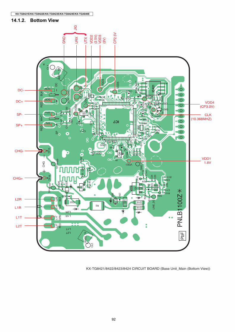
92
KX-TG8421E/KX-TG8422E/KX-TG8423E/KX-TG8424E/KX-TGA840E
14.1.2. Bottom View
KX-TG8421/8422/8423/8424 CIRCUIT BOARD (Base Unit_Main (Bottom View))A
PN
LB11
00Z
CH
G
SP
L2TL1T
L1RL2R
1
80
EE
E
1
CLK
VD
D5
VD
D4
VD
D3
VD
D2
UTX
J101
RE
DW
HT
RE
DB
LK GN
D
AN
T1_T
PCL1
JTA
G
UR
X
4
E
DC
PbF
C421
C422C631
C625
C72
C137 C53C55
C54
C148
C423C84
C147
C826
C820
C305
C65C614
C61
VDD1
C617
C814
R76
R77R78
R75
R34
R81
R33
R37R36
R615
IC7SPp
DCP
DCM
SPmQ421
Q9
AN
T2_T
P
CL2
C62
3C
626
C15
5
LIN
E_D
C
C18
C22 C
56
C16
7
C14
1
C24
C23
C85
7
C85
6
C85
5
C52
C16
9C
170
C13
6
C17
1
C16
8
C14
9 C74
C83
7C
75
C14
5C
146 C15
0
C85
8
R20
R23
R18R
24R
116
R12
R13
R35
R32
R87
R86
L2R
L1R
L2T
L1T
BLK
YLW
RE
DG
RN
TP10
D23
D26
D21
Q2
C622
C14
C57
R19
R117
R29
R2
TP9
D22
D16
D15
Q5
GN
D_C
Q8
C61
5
C43
0
C60
C63
0
C61
6
R42
4R
425
R43
0
R42
6 R42
9
R42
8R
427
IC42
1
TP16
-sub
TP16
TP15
-sub
TP15
RA
80
RA
1
VDD11.8V
CLK(10.368MHZ)
VDD4(CP3.0V)
L2T
L1T
L1R
L2R
SP+
SP-
CHG-
DC+
DC-
GN
D
VD
D3
(3V
)
CP
2.5V
UR
XJI
G
UTX
VD
D2
(2.5
V)
CHG+

93
KX-TG8421E/KX-TG8422E/KX-TG8423E/KX-TG8424E/KX-TGA840E
14.2. Circuit Board (Base Unit_Operation)14.2.1. Component View
ERASE
STOP
KEYS_E KEYS_C KEYS_B MEG_LEDKEYIN2
KEYS_D KEYIN3 KEYIN1 ANS_LED 2APVCC
ANS1
LOCAT/INT
A
DOWN
LED902
LED901
SKIPMSG1 MSG2RPT
UP
KX-TG7431/8421/8431HPNLB1092Z
PbF
KX-TG8421/8422/8423/8424 CIRCUIT BOARD (Base Unit_Operation (Component View))
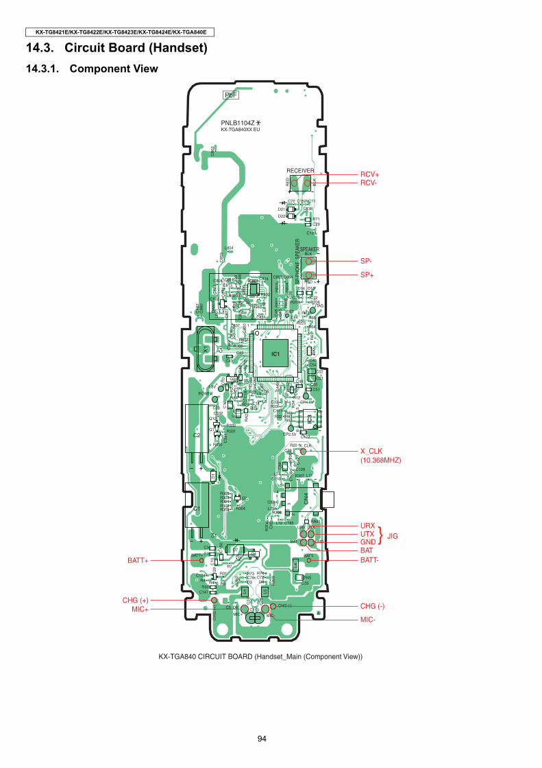
94
KX-TG8421E/KX-TG8422E/KX-TG8423E/KX-TG8424E/KX-TGA840E
14.3. Circuit Board (Handset)14.3.1. Component View
KX-TGA840 CIRCUIT BOARD (Handset_Main (Component View))
A
PbF
PNLB1104ZKX-TGA840XX EU
C138
C71C152C70
RECEIVER
C139
SPEAKER
C29
C802 C72
C813C811C804
C73
C147
C121
C5
C3
F1
C76 C77
C113
C54C40
C44C834
C814 C863 C864
C43
C47
C83
C185
C35
C39
C110
4
5
1
X_CLK
POWER
1.8V
C128
C2
C1
C172
CP4.0V
CP2.5V
C111
C33
C6
C7
C837
C14C13
C38C332
C51C55
C53
C52
C49
R71
R209 R208
R63R66
R64R225
R802
R805
R6
R74R73R31
R7
R30R4R8
R45
R300R303R301R302R305
R12
R42R41R40
R32
R33R25
R203
R807
R22
R28
R332
R330
R331
R306R304
R20
R307
L804
L802
L3
L9
L72
L73
L74 L71
IC1
TEST
JTAG
RA61
BATT-BATT+
RA4
D21
D22
D14 D13
BLK
RED
BLK
RE
D
D8
D7
D4D3
Q4
Q7
Q11
Q12
Q2
C45
C3
6
C46C8
60
C1
82
C8
19
C8
25
C8
27 C
80
9C
81
0C
80
5
C808
C8
61
C8
12
C8
59
C8
62
C8
03
C8
06
CN
4
C7
4
C7
5
C4
C1
5
C1
50
C1
88
C9
7C9
6
C8
22
C8
26
C4
1
X1
C8
20
C1
8C1
1C1
0C
12
C1
6
C3
31
C1
84
C1
7
C4
8
C5
0
C1
09
C8
2
32
11
4
85
1
C1
08
C8
6 C1
27
R6
5
R8
08
R8
01
R8
06
R8
03
R8
04 SP
-PH
ON
E_SP
EAKE
R
R3
10
R3
09
R2
R2
15
R2
7
R1
52
R3
4
R3
08
R1
00
L8
01
L8
03
L5
L4
L8
IC801
IC3
RA
1
RA
2
DA
80
1D
1Q
9
UTXURX
GND
CHG (-)
CH
G (
+)
BAT
MIC-MIC+
BATT+
CHG (+)MIC+
GNDBATBATT-
UTXURX
RCV-RCV+
CHG (-)
JIG
X_CLK(10.368MHZ)
SP+
MIC-
SP-
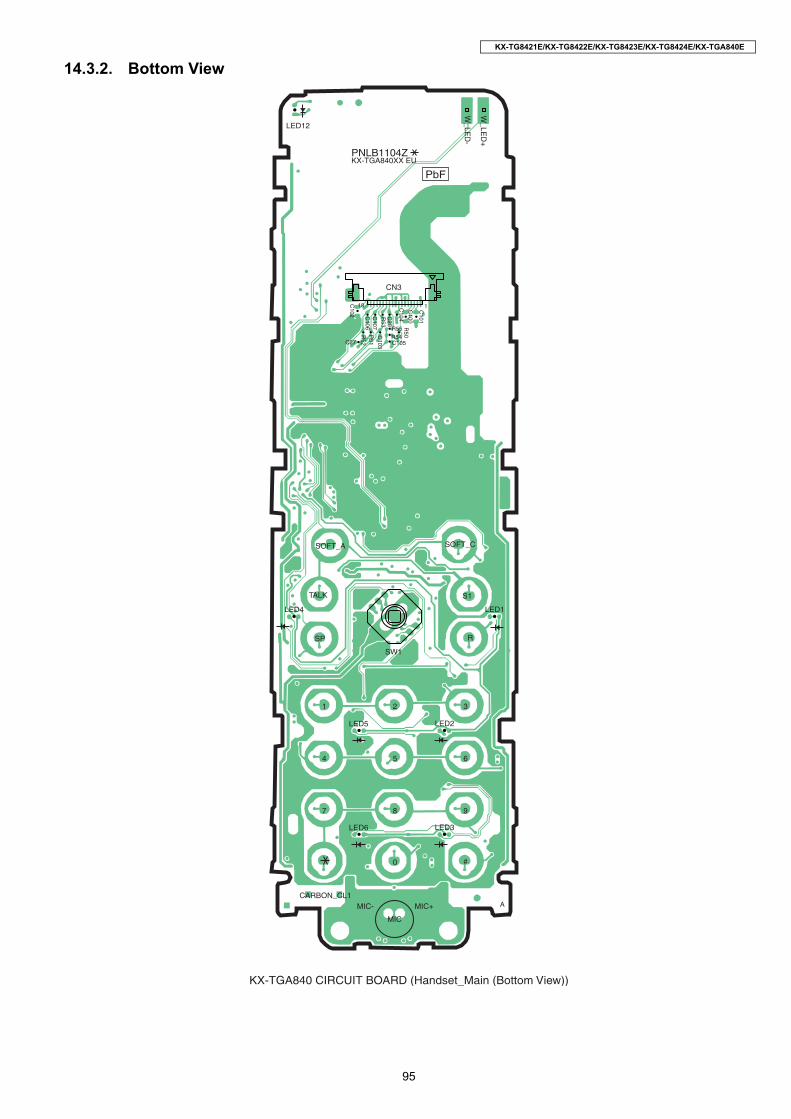
95
KX-TG8421E/KX-TG8422E/KX-TG8423E/KX-TG8424E/KX-TGA840E
14.3.2. Bottom View
1
SP R
2
5
SW1
S1TALK
SOFT_CSOFT_A
3
4 6
7
CARBON_CL1MIC- MIC+
MIC
8 9
LED6 LED3
LED5 LED2
LED12
W_LE
D-
W_LE
D+
LED1LED4
0 #
KX-TGA840 CIRCUIT BOARD (Handset_Main (Bottom View))
CN3
118C102
C100
C104C
106C
107C
103C27 C105
R55
R54
R52
R51
R53
C28
C101
R50
A
PbF
PNLB1104ZKX-TGA840XX EU
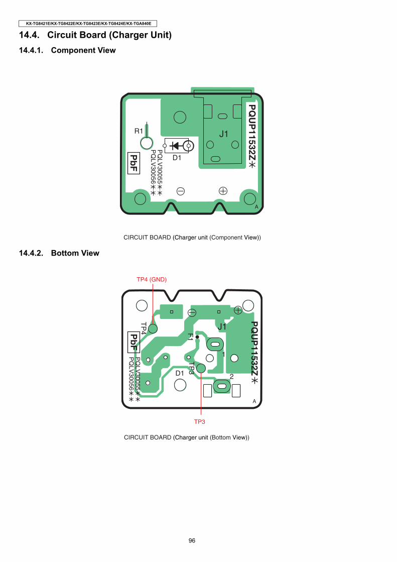
96
KX-TG8421E/KX-TG8422E/KX-TG8423E/KX-TG8424E/KX-TGA840E
14.4. Circuit Board (Charger Unit)14.4.1. Component View
14.4.2. Bottom View
J1R1
D1
A
PQ
UP
11532ZPb
F
PQ
LV30055
PQ
LV30056
CIRCUIT BOARD (Charger unit (Component View))
TP
4
TP
3
1
2
J1
D1
A
F1Pb
FP
QLV
30055P
QLV
30056
PQ
UP
11532Z
CIRCUIT BOARD (Charger unit (Bottom View))
TP4 (GND)
TP3
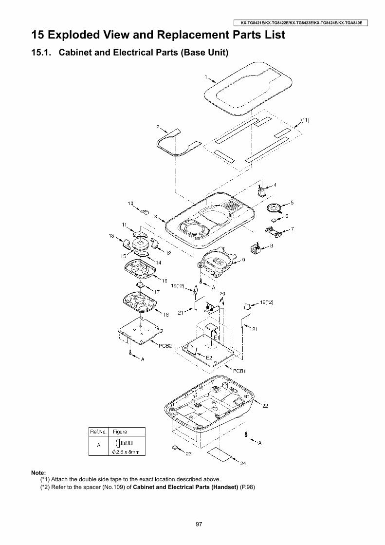
97
KX-TG8421E/KX-TG8422E/KX-TG8423E/KX-TG8424E/KX-TGA840E
15 Exploded View and Replacement Parts List15.1. Cabinet and Electrical Parts (Base Unit)
Note:(*1) Attach the double side tape to the exact location described above.(*2) Refer to the spacer (No.109) of Cabinet and Electrical Parts (Handset) (P.98)
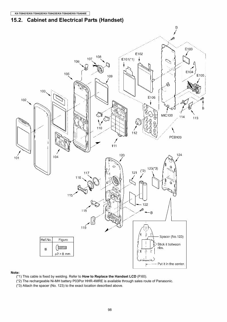
98
KX-TG8421E/KX-TG8422E/KX-TG8423E/KX-TG8424E/KX-TGA840E
15.2. Cabinet and Electrical Parts (Handset)
Note:(*1) This cable is fixed by welding. Refer to How to Replace the Handset LCD (P.60).(*2) The rechargeable Ni-MH battery P03Por HHR-4MRE is available through sales route of Panasonic.(*3) Attach the spacer (No. 123) to the exact location described above.
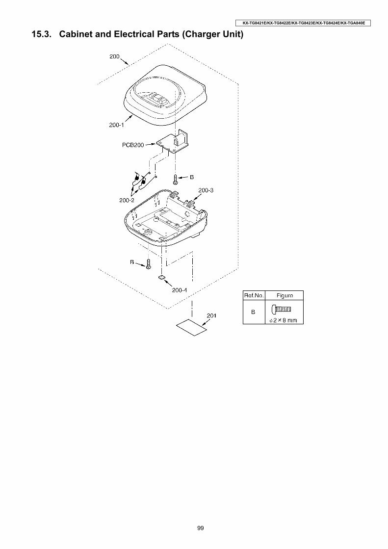
99
KX-TG8421E/KX-TG8422E/KX-TG8423E/KX-TG8424E/KX-TGA840E
15.3. Cabinet and Electrical Parts (Charger Unit)
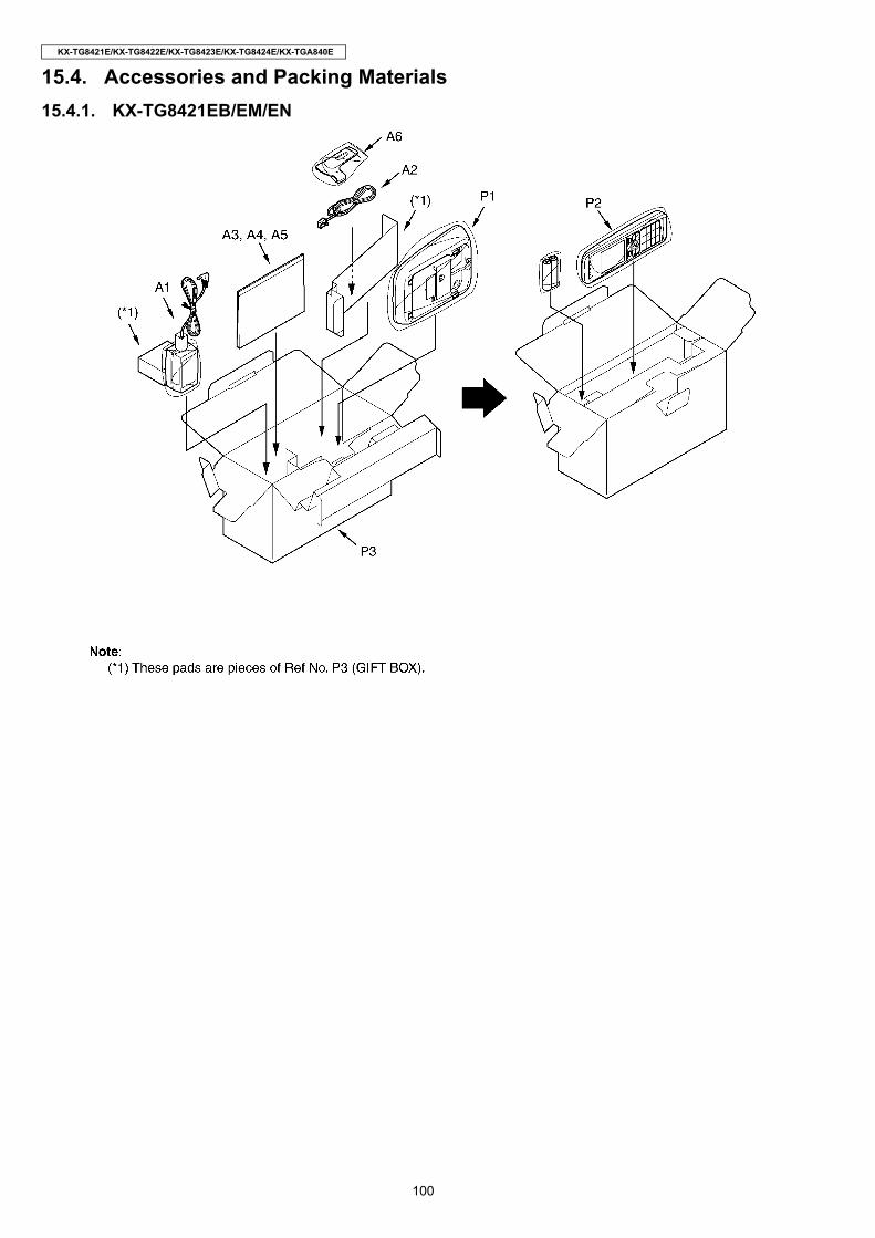
100
KX-TG8421E/KX-TG8422E/KX-TG8423E/KX-TG8424E/KX-TGA840E
15.4. Accessories and Packing Materials15.4.1. KX-TG8421EB/EM/EN

101
KX-TG8421E/KX-TG8422E/KX-TG8423E/KX-TG8424E/KX-TGA840E
15.4.2. KX-TG8422EB/EM/EN

102
KX-TG8421E/KX-TG8422E/KX-TG8423E/KX-TG8424E/KX-TGA840E
15.4.3. KX-TG8423EB/EM/EN
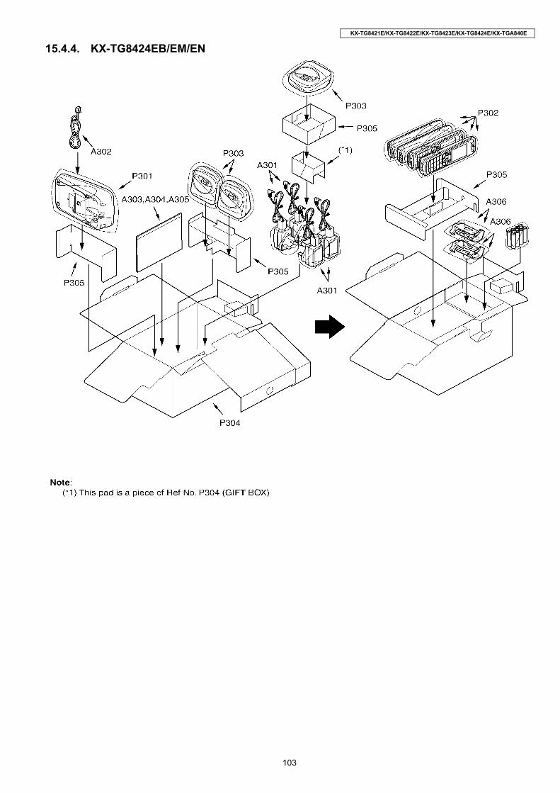
103
KX-TG8421E/KX-TG8422E/KX-TG8423E/KX-TG8424E/KX-TGA840E
15.4.4. KX-TG8424EB/EM/EN

104
KX-TG8421E/KX-TG8422E/KX-TG8423E/KX-TG8424E/KX-TGA840E
15.4.5. KX-TGA840EB/EM/EN

105
KX-TG8421E/KX-TG8422E/KX-TG8423E/KX-TG8424E/KX-TGA840E
15.5. Replacement Part List1. RTL (Retention Time Limited)
Note:The “RTL” marking indicates that its Retention Time isLimited. When production is discontinued, this item will con-tinue to be available only for a specific period of time.This period of time depends on the type of item, andthe local laws governing parts and product retention.At the end of this period, the item will no longer beavailable.
2. Important safety noticeComponents identified by the mark indicates specialcharacteristics important for safety. When replacing anyof these components, only use specified manufacture’sparts.
3. The S mark means the part is one of some identical parts.For that reason, it may be different from the installed part.
4. ISO code (Example: ABS-94HB) of the remarks columnshows quality of the material and a flame resisting gradeabout plastics.
5. RESISTORS & CAPACITORSUnless otherwise specified;All resistors are in ohms (Ω) k=1000 Ω, M=1000 kΩAll capacitors are in MICRO FARADS (µF)p=µµF*Type & Wattage of Resistor
15.5.1. Base Unit15.5.1.1. Cabinet and Electrical Parts
15.5.1.2. Main P.C.Board PartsNote:
(*1) When replacing IC7, IC401 or X1, make the adjustmentusing PNZZTG8421E. Refer to Base Unit (P.68) of Thingsto Do after Replacing IC or X'tal.(*2) When you removing E1, use special tools (ex. Hot airdisordering tool).(*3) Backside of this IC has a ground plate.(*4) Supplied IC is Flat Package Type.
Safety Ref. No.
Part No. Part Name & Description Remarks
1 PNGP1050Y1 PANEL,LCD (for KX-TG8421EB)
ABS-HB
1 PNGP1050X4 PANEL,LCD (for KX-TG8421EM)
ABS-HB
1 PNGP1050X3 PANEL,LCD (for KX-TG8421EN)
ABS-HB
2 PNGG1035Z1 GRILLE (for KX-TG8421EB) ABS-HB2 PNGG1035Z2 GRILLE (for KX-TG8421EM/
EN)ABS-HB
3 PNKM1071Y1 CABINET BODY (for KX-TG8421EB)
ABS-HB
3 PNKM1071X3 CABINET BODY (for KX-TG8421EM)
ABS-HB
3 PNKM1071X2 CABINET BODY (for KX-TG8421EN)
ABS-HB
4 K2ECYZ000001 JACK,DC5 L0AD02A00026 SPEAKER6 PQHG10729Z RUBBER PARTS,SPEAKER7 PQHR11313Z GUIDE,SPEAKER ABS-HB8 PQJJ1T039Y JACK,MODULAR9 PNKE1028Z1 CASE,CHARGE TERMINAL (for
KX-TG8421EB)PS-HB
9 PNKE1028Z2 CASE,CHARGE TERMINAL (forKX-TG8421EM/EN)
PS-HB
10 PNHR1104Z OPTI CCONDUCTIVEPARTS,LED LENS
PS-HB
11 PNBC1023Z1 BUTTON,ERASE ABS-HB12 PNBC1266Y1 BUTTON,ANSWER ON ABS-HB13 PNBC1024Z1 BUTTON,STOP ABS-HB14 PNBC1025Z1 BUTTON,LOCATOR ABS-HB15 PNBC1018Z1 BUTTON,NAVIGATOR KEY (for
KX-TG8421EB)ABS-HB
15 PNBC1018Y5 BUTTON,NAVIGATOR KEY (forKX-TG8421EM)
ABS-HB
15 PNBC1018Y4 BUTTON,NAVIGATOR KEY (forKX-TG8421EN)
ABS-HB
16 PNHR1010Z GUIDE,BUTTON PS-HB17 PNBC1001Z2 BUTTON,MESSAGE (for KX-
TG8421EB/EM)AS-HB
17 PNBC1001Z5 BUTTON,MESSAGE (for KX-TG8421EN)
AS-HB
18 PNJK1047Z KEYBOARD SWITCH19 PNYE1011Z SPACER,ANTENNA20 PNJT1025Z CHARGE TERMINAL21 PNLA1002Z ANTENNA22 PNKF1054X1 CABINET COVER (for KX-
TG8421EB/EM)PS-HB
22 PNKF1054X2 CABINET COVER (for KX-TG8421EN)
PS-HB
23 PQHA10023Z RUBBER PARTS,FOOT24 PNGT1828Z NAME PLATE (for KX-
TG8421EB)24 PNGT1828X NAME PLATE (for KX-
TG8421EM)24 PNGT1828Y NAME PLATE (for KX-
TG8421EN)
Safety Ref. No.
Part No. Part Name & Description Remarks
PCB1 PNWP1G8421EH MAIN P.C.BOARD ASS'Y(RTL)
(ICs)IC1 C0CBAYG00016 IC IC7 C1CB00002906 IC (BBIC(FLASH))
(*1)(*3)(*4)S
IC401 PQWICD300EHR IC (EEPROM) (*1)IC421 C3FBMY000195 ICIC801 C1CB00001842 IC (*3)
(TRANSISTORS)Q3 B1ACGP000007 TRANSISTOR(SI)Q4 PQVTBF822T7 TRANSISTOR(SI)Q5 2SD0874AS TRANSISTOR(SI)Q8 B1ADGE000004 TRANSISTOR(SI)Q9 B1ADGE000004 TRANSISTOR(SI)Q421 2SC6054JSL TRANSISTOR(SI)
(DIODES)D1 B0JCME000035 DIODE(SI)
Safety Ref. No.
Part No. Part Name & Description Remarks

106
KX-TG8421E/KX-TG8422E/KX-TG8423E/KX-TG8424E/KX-TGA840E
D3 B0EDER000009 DIODE(SI)D5 MA111 DIODE(SI) SD6 MA111 DIODE(SI) SD9 MA111 DIODE(SI) SD21 PQVDRLZ20A DIODE(SI) SD22 B0ECKM000008 DIODE(SI)D23 MA8220 DIODE(SI) SDA801 B0DDCD000001 DIODE(SI)DA802 B0DDCD000001 DIODE(SI)
(COILS)L1 PQLQXF330K COIL SL2 PQLQXF330K COIL SL801 G1C27NJ00010 COIL SL802 G1C3N0ZA0063 COILL803 G1C3N0ZA0063 COIL
(COMPONENT PARTS)RA1 D1H810240004 RESISTOR ARRAY SRA402 D1H410320002 RESISTOR ARRAYRA501 EXB28VR000X RESISTOR ARRAYRA80 D1H422120001 RESISTOR ARRAY
(VARISTOR) SA1 J0LF00000026 VARISTOR (SURGE
ABSORBER)
(RESISTORS)R3 PQ4R10XJ184 180k SR4 PQ4R10XJ105 1M SR5 PQ4R10XJ184 180k SR6 PQ4R10XJ105 1M SR7 ERJ3GEYJ565 5.6MR8 ERJ3GEYJ104 100kR9 ERJ3GEYJ565 5.6MR10 ERJ3GEYJ104 100kR14 ERJ3GEYJ104 100kR15 PQ4R10XJ272 2.7k SR16 ERJ2GEJ103 10kR17 ERJ2GEJ222 2.2kR18 ERJ2GEJ273X 27kR19 ERJ2GEJ822 8.2kR20 ERJ2GEJ182 1.8kR21 ERJ12YJ120 12R22 ERJ12YJ270 27R23 ERJ2GEJ104 100kR24 ERJ2GEJ473 47kR27 ERJ2GEJ104 100kR28 ERJ2GEYJ474 470k SR29 ERJ2GEJ121 120R30 ERJ3GEYJ391 390R31 ERJ3GEYJ182 1.8kR32 ERJ2GEJ823 82kR33 ERJ2GEJ102 1kR34 ERJ2GEJ823 82kR35 ERJ2GEJ102 1kR36 ERJ2GEJ124 120kR37 ERJ2GEJ102 1kR38 ERJ2RKF1000 100R39 ERJ2RKF1400 140R42 PQ4R10XJ475 4.7M SR43 PQ4R10XJ475 4.7M SR55 ERJ1TYJ3R9U 3.9R56 ERJ1TYJ3R9U 3.9R75 ERJ2GEJ101 100R76 ERJ2GEJ102 1kR77 ERJ2GEJ103 10kR81 ERJ2GEJ332 3.3kR106 ERJ2GEJ221 220R109 ERJ2GEJ221 220R116 ERJ2GEJ101 100R117 ERJ2GEJ332 3.3kR129 ERJ2GEJ103 10kR130 ERJ2GEJ102 1kR135 ERJ2GEJ103 10kR424 ERJ2GEJ103 10kR425 ERJ2GEJ274 270k
Safety Ref. No.
Part No. Part Name & Description Remarks
R426 ERJ2GEJ561 560R427 ERJ2GEJ561 560R428 ERJ2GEJ561 560R429 ERJ2GEJ332 3.3kR430 ERJ2GEJ100 10R511 ERJ2GE0R00 0R516 ERJ2GE0R00 0R532 ERJ2GE0R00 0R542 ERJ2GE0R00 0R615 D0GA563ZA006 56kR657 ERJ2GEJ103 10kR801 ERJ2GEJ152 1.5kR802 ERJ2GEJ121 120R803 ERJ2GEJ102 1kR804 ERJ2GEJ102 1kR805 ERJ2GEJ470 47R806 ERJ2GEJ221 220R807 ERJ2GEJ221 220R808 ERJ2GEJ152 1.5k
(CAPACITORS)C3 F1K2H681A008 680pC4 F1K2H681A008 680pC5 ECUV1C103KBV 0.01C6 ECUV1C103KBV 0.01C7 ECUV1C104KBV 0.1C8 ECUV1C104KBV 0.1C9 F1K2H681A008 680pC10 F1K2H681A008 680pC14 ECUE1E472KBQ 0.0047C15 PQCUV1A105KB 1C16 PQCUV1A225KB 2.2C17 PQCUV1A225KB 2.2C22 PQCUV1A105KB 1C23 ECJ0EB0J224K 0.22 SC25 ECUE1C103KBQ 0.01C27 F2A1H100B132 10C28 PQCUV1H104ZF 0.1 SC29 F1G1H5R0A480 5pC30 F1G1H5R0A480 5pC31 PQCUV1A225KB 2.2C32 F2A1C1010119 100C36 F2A1A3310040 330C37 F1G1H5R0A480 5pC42 ECUV1C103KBV 0.01C43 ECUV1C103KBV 0.01C51 ECUE1A104KBQ 0.1C52 ECUE1H821KBQ 820pC53 ECUE1H821KBQ 820pC54 ECUE1A333KBQ 0.033C55 ECUE1A823KBQ 0.082C56 ECUV1C104KBV 0.1C60 ECUE1A104KBQ 0.1C61 ECUE1A104KBQ 0.1C65 ECUE1H100DCQ 10pC70 ECUE1H100DCQ 10pC72 ECUE1A104KBQ 0.1C74 ECUE1H100DCQ 10pC75 ECUE1A104KBQ 0.1C84 ECUV1A225KB 2.2C136 ECUE1H100DCQ 10pC137 ECUE1H100DCQ 10pC141 ECJ0EB0J224K 0.22 SC145 ECUE1H100DCQ 10pC146 ECUE1H100DCQ 10pC147 ECUE1H100DCQ 10pC148 ECUE1H100DCQ 10pC149 ECUE1H222KBQ 0.0022C150 ECUE1H222KBQ 0.0022C157 ECUE1H102KBQ 0.001C168 ECUE1H100DCQ 10pC169 ECUE1H100DCQ 10pC170 ECUE1H100DCQ 10pC171 ECUE1H100DCQ 10p
Safety Ref. No.
Part No. Part Name & Description Remarks

107
KX-TG8421E/KX-TG8422E/KX-TG8423E/KX-TG8424E/KX-TGA840E
15.5.1.3. Operational P.C.Board Parts
15.5.2. Handset15.5.2.1. Cabinet and Electrical Parts
15.5.2.2. Main P.C.Board PartsNote:
(*1) Reconfirm the model No. written on the handset’s nameplate when replacing PCB100. Because the model No. ofthe optional handset may differ from the included handset.(*2) When replacing IC1, IC3 or X1, make the adjustmentusing PNZZTG8421E. Refer to Handset (P.69) of Thingsto Do after Replacing IC or X'tal.(*3) When you removing E103, use special tools (ex. Hot airdisordering tool).
C305 ECUE0J105KBQ 1C421 ECUE1C103KBQ 0.01C422 ECUE1A104KBQ 0.1C511 ECUE1H100DCQ 10pC512 ECUE1H100DCQ 10pC513 ECUE1H100DCQ 10pC514 ECUE1H100DCQ 10pC515 ECUE1H100DCQ 10pC516 ECUE1H100DCQ 10pC517 ECUE1H100DCQ 10pC518 ECUE1H100DCQ 10pC519 ECUE1H100DCQ 10pC614 ECUV1A105KBV 1C615 ECUV1A105KBV 1C616 ECUV1A105KBV 1C617 ECUV1A105KBV 1C625 ECUV1A105KBV 1C630 ECUE1H100DCQ 10pC631 ECUE1H100DCQ 10pC802 F1G1H1R8A480 1.8pC803 F1G1H1R5A480 1.5pC804 F1G1H1R8A480 1.8pC805 F1G1H3R3A480 3.3pC806 F1G1H3R3A480 3.3pC808 ECUE1A104KBQ 0.1C809 ECUE1H100DCQ 10pC810 F1G1H2R2A480 2.2pC811 ECUE1H100DCQ 10pC812 ECUE1H100DCQ 10pC813 F1G1H2R2A480 2.2pC814 ECUE1H332KBQ 0.0033C819 ECUE1H100DCQ 10pC820 F1G1HR75A480 0.75pC822 ECUE1H100DCQ 10pC823 ECUE1H101JCQ 100pC825 ECUE1H100DCQ 10pC826 F1G1HR90A480 0.9pC827 ECUE1H100DCQ 10pC834 F1G1HR50A480 0.5pC851 F1G1H2R0A480 2pC853 F1G1H2R0A480 2pC855 ECUE1H100DCQ 10pC856 ECUE1H101JCQ 100pC857 ECUE1H100DCQ 10pC858 ECUE1H101JCQ 100pC859 ECUE1H100DCQ 10pC860 F1G1H3R0A480 3pC861 ECUE1H100DCQ 10p
(OTHERS)E1 PNMC1013Z CASE,MAGNETIC SHIELD(*2)E2 WBX10SH-3.5G LEAD WIRE, PARALLEL WIREX1 H0J103500027 CRYSTAL OSCILLATOR (*1) F1 K5H302Y00003 FUSE
Safety Ref. No.
Part No. Part Name & Description Remarks
PCB2 PNWP2G7431H OPERATIONAL P.C.BOARDASS'Y (RTL)
(DIODES)LED901 PQVDBR1111C LED SLED902 PQVDBR1111C LED S
Safety Ref. No.
Part No. Part Name & Description Remarks
101 PNGP1047Z1 PANEL,LCD (for KX-TGA840EB)
PMMA-HB
Safety Ref. No.
Part No. Part Name & Description Remarks
101 PNGP1047Z3 PANEL,LCD (for KX-TGA840EM)
PMMA-HB
101 PNGP1047Z2 PANEL,LCD (for KX-TGA840EN)
PMMA-HB
102 PNGG1032Z1 GRILL,FRAME (for KX-TGA840EB)
ABS-HB
102 PNGG1032Z2 GRILL,FRAME (for KX-TGA840EM/EN)
ABS-HB
103 PNYE1013Z TAPE,DOUBLESIDED104 PNGG1033Z1 GRILLE (for KX-TGA840EB) ABS-HB104 PNGG1033Y3 GRILLE (for KX-TGA840EM) ABS-HB104 PNGG1033Y2 GRILLE (for KX-TGA840EN) ABS-HB105 PNKM1069Z1 CABINET BODY (for KX-
TGA840EB)ABS-HB
105 PNKM1069Y3 CABINET BODY (for KX-TGA840EM)
ABS-HB
105 PNKM1069Y2 CABINET BODY (for KX-TGA840EN)
ABS-HB
106 PNHR1105Z OPTIC CONDUCTIVE-PARTS,LED LENS
PS-HB
107 L0AD01A00017 RECEIVER108 PQHG10729Z RUBBER PARTS,RECEIVER109 PNYE1011Z SPACER,LCD110 PNBX1047Z1 BUTTON,CURSOL KEY (for
KX-TGA840EB)ABS-HB
110 PNBX1047Y3 BUTTON,CURSOL KEY (forKX-TGA840EM)
ABS-HB
110 PNBX1047Y2 BUTTON,CURSOL KEY (forKX-TGA840EN)
ABS-HB
111 PNYT1013Z1 KEYBOARD SWITCH (for KX-TGA840EB)
111 PNYT1013Z3 KEYBOARD SWITCH (for KX-TGA840EM)
111 PNYT1013Y2 KEYBOARD SWITCH (for KX-TGA840EN)
112 PNBC1267Z1 PUSH BUTTON (for KX-TGA840EB)
112 PNBC1267Z2 PUSH BUTTON (for KX-TGA840EM/EN)
113 PNJT1026Z CHARGE TERMINAL(R)114 PNJT1027Z CHARGE TERMINAL(L)115 PQHR11315Z GUIDE,SPEAKER ABS-HB116 L0AA02A00095 SPEAKER117 PQHS10784Y SPACER,SPEAKER NET118 PQJC10056X BATTERY TERMINAL119 PNKE1027Z1 COVER,EP CAP (for KX-
TGA840EB/EM)119 PNKE1027Z3 COVER,EP CAP (for KX-
TGA840EN)120 PNKF1052Z1 CABINET COVER (for KX-
TGA840EB/EM)ABS-HB
120 PNKF1052Z2 CABINET COVER (for KX-TGA840EN)
ABS-HB
121 PNQT23182Z ATTENTION LABEL122 PNGT1829Z NAME PLATE (for KX-
TGA840EB)122 PNGT1829X NAME PLATE (for KX-
TGA840EM)122 PNGT1829Y NAME PLATE (for KX-
TGA840EN)123 PNHS1079Z SPACER,BATTERY124 PNKK1028Z1 LID,BATTERY (for KX-
TGA840EB/EM)ABS-HB
124 PNKK1028Z2 LID,BATTERY (for KX-TGA840EN)
ABS-HB
Safety Ref. No.
Part No. Part Name & Description Remarks

108
KX-TG8421E/KX-TG8422E/KX-TG8423E/KX-TG8424E/KX-TGA840E
(*4) When replacing the handset LCD, See How toReplace the Handset LCD(P.60).(*5) Backside of this IC has a ground plate.(*6) Supplied IC is Flat Package Type.
Safety Ref. No.
Part No. Part Name & Description Remarks
PCB100 PNWPGA840EXR MAIN P.C.BOARD ASS'Y(RTL) (*1)(ICs)
IC1 C1CB00002906 IC (BBIC (FLASH)) (*2)(*5)(*6)
IC3 PQWIA130EXRR IC (EEPROM) (*2) IC801 C1CB00001842 IC (*5)
(TRANSISTORS)Q2 B1ADGE000004 TRANSISTOR(SI) Q4 B1ADGE000004 TRANSISTOR(SI) Q7 UN9219J TRANSISTOR(SI) SQ9 2SC6054JSL TRANSISTOR(SI) Q11 B1ADCF000161 TRANSISTOR(SI)Q12 B1ADCF000161 TRANSISTOR(SI)
(DIODES)D1 MA2YD2120L DIODE(SI) D7 B0JCME000035 DIODE(SI) D21 MA8043M DIODE(SI) SD22 MA8043M DIODE(SI) SDA801 B0DDCD000001 DIODE(SI)LED1 B3AEB0000124 LEDLED2 B3AEB0000124 LEDLED3 B3AEB0000124 LEDLED4 B3AEB0000124 LEDLED5 B3AEB0000124 LEDLED6 B3AEB0000124 LEDLED12 B3ACB0000216 LED
(COILS)L801 G1C27NJ00010 COILL802 G1C3N6ZA0063 COIL L803 G1C3N6ZA0063 COIL F1 PQLQR2M5N6K COIL S
(COMPONENTS PARTS)RA1 D1H810240004 RESISTOR ARRAY SRA2 D1H410220001 RESISTOR ARRAYRA4 D1H433220001 RESISTOR ARRAYRA61 D1H422120001 RESISTOR ARRAY
(VARISTORS)D13 D4ZZ00000024 VARISTOR D14 D4ZZ00000024 VARISTOR
(CONNECTORS)CN3 K1MN18BA0111 CONNECTORCN4 K2HD103D0001 CONNECTOR
(IC FILTERS)L9 J0JCC0000287 IC FILTER L72 J0JCC0000276 IC FILTER R308 J0JCC0000286 IC FILTER
(RESISTORS)R2 ERJ2GEJ392 3.9kR6 ERJ2GEJ102 1kR7 ERJ2GEJ122 1.2kR8 ERJ2GEJ101 100R12 ERJ2GE0R00 0R20 ERJ2GEJ100 10R22 ERJ2GEJ332 3.3kR25 ERJ2GEJ222 2.2kR27 ERJ2GEJ821 820R28 ERJ2GEJ821 820R30 ERJ3GEYJ273 27kR32 ERJ2GEJ104 100kR33 ERJ2GE0R00 0R34 ERJ2GEJ104 100kR40 ERJ2GEJ103 10kR41 ERJ2GEJ103 10kR42 ERJ2GEJ103 10kR45 ERJ6RSJR10V 0.1R50 ERJ2GEJ332 3.3k
R51 ERJ2GEJ471 470R52 ERJ2GEJ221 220R53 ERJ2GEJ332 3.3kR54 ERJ2GEJ103 10kR55 ERJ2GEJ102 1kR63 ERJ2GEJ101 100R64 ERJ2GEJ103 10kR66 ERJ2GEJ102 1kR71 ERJ3GEYJ820 82R73 ERJ2GEJ820 82R74 ERJ2GEJ820 82R203 D0GA563ZA006 56kR208 ERJ2GE0R00 0R209 ERJ2GE0R00 0R215 ERJ2GE0R00 0R225 ERJ2GE0R00 0R300 ERJ2GEJ271 270R301 ERJ2GEJ271 270R302 ERJ2GEJ271 270R303 ERJ2GEJ271 270R304 ERJ2GEJ271 270R305 ERJ2GEJ271 270R306 ERJ2GEJ101 100R330 ERJ2GEJ105X 1MR331 ERJ2GEJ273X 27kR332 ERJ2GEJ273X 27kR801 ERJ2GEJ681 680R802 ERJ2GEJ101 100R803 ERJ2GEJ102 1kR804 ERJ2GEJ102 1kR805 ERJ2GEJ470 47R806 ERJ2GEJ221 220R807 ERJ2GEJ221 220L74 ERJ2GEJ100 10
(CAPACITORS)C1 F2A0J3310067 330C2 F2A0J3310067 330C5 ECUE1A104KBQ 0.1C10 ECUV1A225KB 2.2C11 ECUE1A104KBQ 0.1C12 PQCUV0J106KB 10C13 ECUE1A104KBQ 0.1C14 ECUE1C103KBQ 0.01C16 PQCUV0J106KB 10C17 ECUE1H100DCQ 10pC18 ECUE1H100DCQ 10pC27 ECUE0J105KBQ 1C29 ECUV1H100DCV 10pC33 ECUE1A104KBQ 0.1C40 ECUE1A104KBQ 0.1C43 ECUE1H100DCQ 10pC44 ECUE1A104KBQ 0.1C45 ECUE1A104KBQ 0.1C46 ECUE1H100DCQ 10pC47 ECUV1A105KBV 1C49 ECUV1A105KBV 1C50 ECUV1A105KBV 1C51 ECUV1A105KBV 1C52 PQCUV0J106KB 10C53 PQCUV0J106KB 10C54 ECUE1H100DCQ 10pC55 ECUE1H100DCQ 10pC70 ECUE1H100DCQ 10pC71 ECUE1H100DCQ 10pC72 ECUE1H100DCQ 10pC73 ECUE1H100DCQ 10pC74 ECUE1H100DCQ 10pC75 ECUE1H100DCQ 10pC82 ECUE1H471KBQ 470pC83 ECUE1H100DCQ 10pC86 PQCUV0J106KB 10C96 ECUE1H100DCQ 10pC97 ECUE1H100DCQ 10p
Safety Ref. No.
Part No. Part Name & Description Remarks

109
KX-TG8421E/KX-TG8422E/KX-TG8423E/KX-TG8424E/KX-TGA840E
15.5.3. Charger Unit15.5.3.1. Cabinet and Electrical Parts
15.5.3.2. Main P.C.Board Parts
15.5.4. Accessories and Packing MaterialsNote:
(*1) You can download and refer to the Operating Instruc-tions (Instruction book) on TSN Server.
15.5.4.1. KX-TG8421EB/EM/EN
15.5.4.2. KX-TG8422EB/EM/EN
C100 F1H1E1050001 1C101 ECUV1C105KBV 1C102 ECUV1C105KBV 1C110 ECUE1H102KBQ 0.001C113 ECUE1H100DCQ 10pC127 ECUE1H102KBQ 0.001C152 ECUE1H102KBQ 0.001C172 ECUV1C104KBV 0.1C184 ECUE1H100DCQ 10pC185 ECUE1H102KBQ 0.001C188 ECUE0J105KBQ 1C331 ECUE0J105KBQ 1C332 ECUE0J105KBQ 1C802 F1G1H2R0A480 2.0pC803 F1G1H1R5A480 1.5p C804 F1G1H2R0A480 2.0p C805 F1G1H3R3A480 3.3pC806 F1G1H3R3A480 3.3pC808 ECUE1A104KBQ 0.1C809 ECUE1H100DCQ 10pC810 F1G1H1R6A480 1.6pC811 ECUE1H100DCQ 10pC812 ECUE1H100DCQ 10pC813 F1G1H1R6A480 1.6p C814 ECUE1H332KBQ 0.0033C819 ECUE1H100DCQ 10pC820 F1G1HR70A480 0.7pC822 ECUE1H100DCQ 10pC825 ECUE1H100DCQ 10pC826 F1G1H2R0A480 2.0pC827 ECUE1H100DCQ 10pC834 F1G1HR50A480 0.5pC859 F1G1H4R0A480 4pC860 ECUE1H100DCQ 10pC861 F1G1H3R0A480 3pC862 F1G1HR50A480 0.5pC863 ECUE1H100DCQ 10pC864 ECUE1H100DCQ 10p
(OTHERS)MIC100 L0CBAY000032 MICROPHONE E101 L5DYDYY00003 LIQUID CRYSTAL DISPLAY
(*4)E102 PQLZ11015Z BACKLIGHT UNITE103 PNMC1013Z CASE,MAGNETIC SHIELD(*2) ABS-HBE104 PNLA1020Z ANTENNAE105 PNVE1002Z BATTERY TERMINALE106 PNJE1022Z SPECIAL SWITCHX1 H0J103500034 CRYSTAL OSCILLATOR (*2) SW1 K0C115A00007 SEESAW SWITCH
Safety Ref. No.
Part No. Part Name & Description Remarks
200 PNLC1007ZB CHARGER UNIT ASS'Ywithout NAME PLATE(for KX-TGA840EB) (RTL)
200 PNLC1007ZM CHARGER UNIT ASS'Ywithout NAME PLATE(for KX-TGA840EM) (RTL)
200 PNLC1007ZN CHARGER UNIT ASS'Ywithout NAME PLATE(for KX-TGA840EN) (RTL)
200-1 PNKM1076Z1 CABINET BODY (for KX-TGA840EB)
PS-HB
200-1 PNKM1076Y4 CABINET BODY (for KX-TGA840EM)
PS-HB
200-1 PNKM1076Y3 CABINET BODY (for KX-TGA840EN)
PS-HB
200-2 PNJT1010Z CHARGE TERMINAL 200-3 PNKF1012Z1 CABINET COVER (for KX-
TGA840EB/EM) ABS-HB
Safety Ref. No.
Part No. Part Name & Description Remarks
200-3 PNKF1012Z5 CABINET COVER (for KX-TGA840EN)
ABS-HB
200-4 PQHA10023Z RUBBER PARTS FOOT CUSHION201 PNGT1837Z NAME PLATE (for KX-
TGA840EB)201 PNGT1837X NAME PLATE (for KX-
TGA840EM)201 PNGT1837Y NAME PLATE (for KX-
TGA840EN)
Safety Ref. No.
Part No. Part Name & Description Remarks
PCB200 PQWPTGA721CH MAIN P.C.BOARD ASS'Y(RTL)
(DIODE)D1 B0JAME000095 DIODE(SI)
(JACK)J1 K2ECYB000001 JACK
(RESISTOR)R1 ERG2SJ100E 10
(FUSE)F1 K5H302Y00003 FUSE
Safety Ref. No.
Part No. Part Name & Description Remarks
A1 PQLV219EY AC ADAPTOR
A2 PQJA87S CORD TELEPHONE A3 PNQX1708Z INSTRUCTION BOOK (*1) A4 PNQW1548Z LEAFLET, QUICK GUIDE A5 PQQW15876Z LEAFLET, SMS GUIDE A6 PNKE1029Z1 HANGER,BELT CLIP (for KX-
TG8421EB/EM)ABS-HB
A6 PNKE1029Z3 HANGER,BELT CLIP (for KX-TG8421EN)
ABS-HB
P1 PNPM1002Z PROTECTION COVER (for BaseUnit)
P2 PQPH10088Z PROTECTION COVER (forHandset)
P3 PNPK1888Z GIFT BOX
Safety Ref. No.
Part No. Part Name & Description Remarks
A101 PQLV219EY AC ADAPTOR
A102 PQJA87S CORD,TELEPHONEA103 PNQX1708Z INSTRUCTION BOOK (*1)A104 PNQW1548Z LEAFLET, QUICK GUIDEA105 PQQW15876Z LEAFLET, SMS GUIDE A106 PNKE1029Z1 HANGER,BELT CLIP (for KX-
TG8422EB/EM)ABS-HB
A106 PNKE1029Z3 HANGER,BELT CLIP (for KX-TG8422EN)
ABS-HB
P101 PNPM1002Z PROTECTION COVER (for BaseUnit)
P102 PQPH10088Z PROTECTION COVER (for Hand-set)
P103 PQPH10101Z PROTECTION COVER (forCharger Unit)
P104 PNPK1889Z GIFT BOXP105 PNPD1154Z CUSHION
Safety Ref. No.
Part No. Part Name & Description Remarks
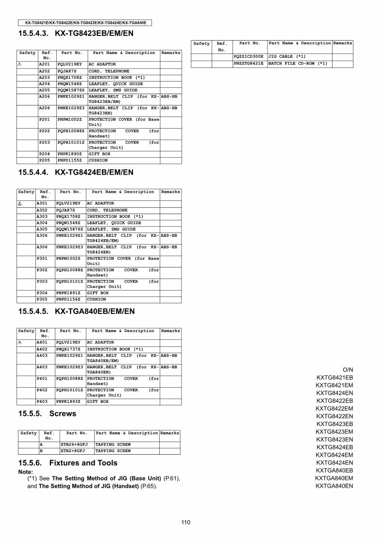
110
KX-TG8421E/KX-TG8422E/KX-TG8423E/KX-TG8424E/KX-TGA840E
15.5.4.3. KX-TG8423EB/EM/EN
15.5.4.4. KX-TG8424EB/EM/EN
15.5.4.5. KX-TGA840EB/EM/EN
15.5.5. Screws
15.5.6. Fixtures and ToolsNote:
(*1) See The Setting Method of JIG (Base Unit) (P.61),and The Setting Method of JIG (Handset) (P.65).
O/NKXTG8421EBKXTG8421EMKXTG8424ENKXTG8422EBKXTG8422EMKXTG8422ENKXTG8423EBKXTG8423EMKXTG8423ENKXTG8424EBKXTG8424EMKXTG8424ENKXTGA840EBKXTGA840EMKXTGA840EN
Safety Ref. No.
Part No. Part Name & Description Remarks
A201 PQLV219EY AC ADAPTOR
A202 PQJA87S CORD, TELEPHONEA203 PNQX1708Z INSTRUCTION BOOK (*1)A204 PNQW1548Z LEAFLET, QUICK GUIDEA205 PQQW15876Z LEAFLET, SMS GUIDEA206 PNKE1029Z1 HANGER,BELT CLIP (for KX-
TG8423EB/EM)ABS-HB
A206 PNKE1029Z3 HANGER,BELT CLIP (for KX-TG8423EN)
ABS-HB
P201 PNPM1002Z PROTECTION COVER (for BaseUnit)
P202 PQPH10088Z PROTECTION COVER (forHandset)
P203 PQPH10101Z PROTECTION COVER (forCharger Unit)
P204 PNPK1890Z GIFT BOXP205 PNPD1155Z CUSHION
Safety Ref. No.
Part No. Part Name & Description Remarks
A301 PQLV219EY AC ADAPTOR
A302 PQJA87S CORD, TELEPHONEA303 PNQX1708Z INSTRUCTION BOOK (*1)A304 PNQW1548Z LEAFLET, QUICK GUIDEA305 PQQW15876Z LEAFLET, SMS GUIDEA306 PNKE1029Z1 HANGER,BELT CLIP (for KX-
TG8424EB/EM)ABS-HB
A306 PNKE1029Z3 HANGER,BELT CLIP (for KX-TG8424EN)
ABS-HB
P301 PNPM1002Z PROTECTION COVER (for BaseUnit)
P302 PQPH10088Z PROTECTION COVER (forHandset)
P303 PQPH10101Z PROTECTION COVER (forCharger Unit)
P304 PNPK1891Z GIFT BOXP305 PNPD1156Z CUSHION
Safety Ref. No.
Part No. Part Name & Description Remarks
A401 PQLV219EY AC ADAPTOR
A402 PNQX1737Z INSTRUCTION BOOK (*1)A403 PNKE1029Z1 HANGER,BELT CLIP (for KX-
TGA840EB/EM)ABS-HB
A403 PNKE1029Z3 HANGER,BELT CLIP (for KX-TGA840EN)
ABS-HB
P401 PQPH10088Z PROTECTION COVER (forHandset)
P402 PQPH10101Z PROTECTION COVER (forCharger Unit)
P403 PNPK1893Z GIFT BOX
Safety Ref. No.
Part No. Part Name & Description Remarks
A XTB26+8GFJ TAPPING SCREWB XTB2+8GFJ TAPPING SCREW
Safety Ref. No.
Part No. Part Name & Description Remarks
PQZZ1CD300E JIG CABLE (*1)
PNZZTG8421E BATCH FILE CD-ROM (*1)