telmo gomes dos santos , pedro m. ramos , pedro ... - imeko · do not enable the detection or...
TRANSCRIPT

16th IMEKO TC4 Symposium Exploring New Frontiers of Instrumentation and Methods for Electrical and Electronic Measurements Sept. 22-24, 2008, Florence, Italy
Non destructive testing of friction stir welding: Comparison of planar eddy current probes
Telmo Gomes dos Santos1, Pedro M. Ramos2, Pedro dos Santos Vilaça1
1IDMEC,DEM, IST, Universidade Técnica de Lisboa, Lisbon, Portugal, [email protected]
2Instituto de Telecomunicações, DEEC, IST, UTL, Lisbon, Portugal, [email protected]
Abstract - Welding of aluminium alloys has undergone a significant development with the Friction Stir Welding (FSW) process. Quality assurance of welded structures is always an important issue for industrial applications and although the good quality of FSW joints, some defects may arise. These defects are difficult or even impossible to detect with conventional non destructive testing (NDT) techniques. This paper presents a detailed analysis about the performance of conventional NDT planar eddy current probes to detect FSW defects. The analysis is based in the impedance measurements of the probes in different standard conditions of lift-off and conductivity. The results show that these types of probes are not enough to deal with the specific FSW defects morphology. Therefore a new type of NDT eddy current probes is proposed and characterized. Comparison results show a higher sensitivity of the new probe.
I. Introduction The Friction Stir Welding Process and Defects Friction Stir Welding (FSW) is a solid state welding process, which proceeds below the melting point of the weld material, i.e., there is no bulk melting in the region of the joint as occurs for conventional fusion welding processes [1]. Instead, the workpieces are joined by the interaction of a rotating non-consumable tool, which is plunged and traversed along the joint line (Figure 1a). The principles behind the technology have been patented and the increase of industrial applications of FSW, namely aerospace, aeronautic, naval and automotive sectors, has been asserting the importance of this process in the scope of joining technologies [2]. In spite of the good quality of FSW beads there are some defects that may arise. Moreover, the microstructural nature of some of these defects (Figure 1b), lead to a very difficult detection when using the existent Non Destructive Testing (NDT) techniques.
a) b)
Figure 1. Friction Stir Welding Process: a) Schematic representation; b) Transversal weld bead
macrography with typical defects on butt joint Eddy Current Probes for NDT of FSW The typical NDT techniques, such as: visual inspection, magnetic particles, liquid penetrant and X-ray, do not enable the detection or quantification of the typical FSW defects, e.g., root defects. The NDT technique more appropriated for that kind of defects is the eddy current test, which is the most

16th IMEKO TC4 Symposium Exploring New Frontiers of Instrumentation and Methods for Electrical and Electronic Measurements Sept. 22-24, 2008, Florence, Italy
commonly NDT technique for detecting small surface defects in metals. This NDT technique involves scanning a wire coil (the eddy current probe) excited by an alternating current across the surface of a metal part. The impedance of the probe is measured as it is scanned. Defects, such as cracks, are detected because they affect the flow of the eddy currents induced in the metal, meaning a decrease of the local conductivity, thereby changing the impedance of the probe. However, this eddy currents flow variations results not only from the presence of defects but is also due to the variations of the probe lift-off from the surface of the material being tested. In fact, the high-sensitive lift-off effect of conventional eddy current probes generates a measurement error which can mask the signal produced by the typical FSW small defects. This makes the detection of those defects difficult or even impossible. This paper presents a detailed analysis about the performance of the conventional planar NDT eddy current probes to detect FSW defects. The reliability of the eddy current probes for NDT applications is strongly dependent of three features (Figure 2): a) a superior response to the conductivity changes when compared to the lift-off influence; b) a higher angle separation between the lift-off and conductivity curves; c) higher relative impedance variation.
σ ↓
↑−offlift
↑f
( )[ ]Re Z Ω
( ) [ ]Im Z Ω
AlZ
AirZ
θ
Figure 2. Typical impedance diagram for a cylindrical helicoidally probe in nonmagnetic material.
III. Experimental procedure
Three different types of planar spiral coils probes were produced and tested: a) 20 circular coils; b) 10 circular coils; c) 10 square coils (Figure 3). All coils were printed on a circuit board and have line width of 100 µm, thickness of 30 µm and distance between successive coils of 100 µm. These types of probes have been suggested [3] to have a high potential for several NDT applications, due to their close proximity to the surface material and the possibility of being printed on a flexible sheet.
a) b) c)
Figure 3. Analysed planar spiral coil probes: a) 20 circular coils; b) 10 circular coils c) 10 square coils. The induced eddy currents are a function of the material conductivity, its magnetic permeability, the measurement frequency and also of the material eventual defects. The lift-off tests were conducted on standard thin film polymers of different thicknesses on top of the material surface and the conductivity tests were carried out on three different materials: Cu, AA2024 (AA stands for Aluminium Alloys) and Pb (99.94-wt%) with 100%, 37.8% and 8.1% of the IACS (International Annealed Copper Standard) respectively. The measurement results were obtained using a Agilent 4294A Precision Impedance Analyzer [4] and the real and imaginary parts of the measured impedance and a remote control application using GPIB. The results for the lift-off measurements are shown in Figure 4 for the AA2024 with 37.8% IACS. For all the probes the influence of the lift-off is clear. Although for the 10 circular coils there is a common impedance value for all lift-offs, this value corresponds to different measurement frequencies and cannot be used to avoid the lift-off measurement problem.
16th IMEKO TC4 Symposium Exploring New Frontiers of Instrumentation and Methods for Electrical and Electronic Measurements Sept. 22-24, 2008, Florence, Italy
0
5
10
15
20
25
30
2 3 4 5
Re(Z) [Ω]
Im(Z) [Ω]
0
5
10
15
0 1 2
Re(Z) [Ω]
Im(Z) [Ω]
0
5
10
15
0 1 2 3
Re(Z) [Ω]
Im(Z) [Ω]
a) b) c)
Figure 4. Real and imaginary components of the measured impedances for the three probes (a) the 20 circular; b) the 10 circular and c) the 10 square) as function of the frequency and the lift-off. The thick lines correspond to constant frequency lines at 100 kHz and 1 MHz. The arrows indicate the increasing lift-offs that correspond to 70 μm, 179 μm, 288 μm, 396 μm, 614 μm, 950 μm, 1980 μm, 3030 μm and
full lift-off. In Figure 5, the results obtained with the three probes and 70 μm of lift-off are shown for the three different materials. From these results it is clear the influence of the material conductivity on the real part of the probe impedance.
0
5
10
15
20
25
30
0 1 2 3 4 5 6
Re(Z) [Ω]
Im(Z) [Ω]
200 kHz
1 MHz
2 MHz
5 MHz
10 MHz
100% IACS
37.8% IACS8,1% IACS
0
5
10
15
0 0.25 0.5 0.75 1 1.25 1.5 1.75 2
Re(Z) [Ω]
Im(Z) [Ω]
200 kHz
1 MHz
2 MHz
5 MHz
10 MHz
100% IACS
37.8% IACS8,1% IACS
0
5
10
15
0 0.5 1 1.5 2 2.5
Re(Z) [Ω]
Im(Z) [Ω]
200 kHz
1 MHz
2 MHz
5 MHz
10 MHz
3
100% IACS37.8% IACS
8,1% IACS
a) b) c)
Figure 5. Real and imaginary components of the measured impedances for the three probes (a) the 20 circular; b) the 10 circular and c) the 10 square) as function of the frequency and the conductivity of the
materials. The thick lines correspond to constant frequency lines at 200 kHz, 1 MHz, 2 MHz, 5 MHz and 10 MHz.
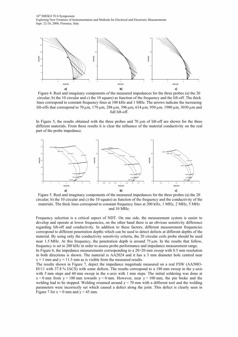
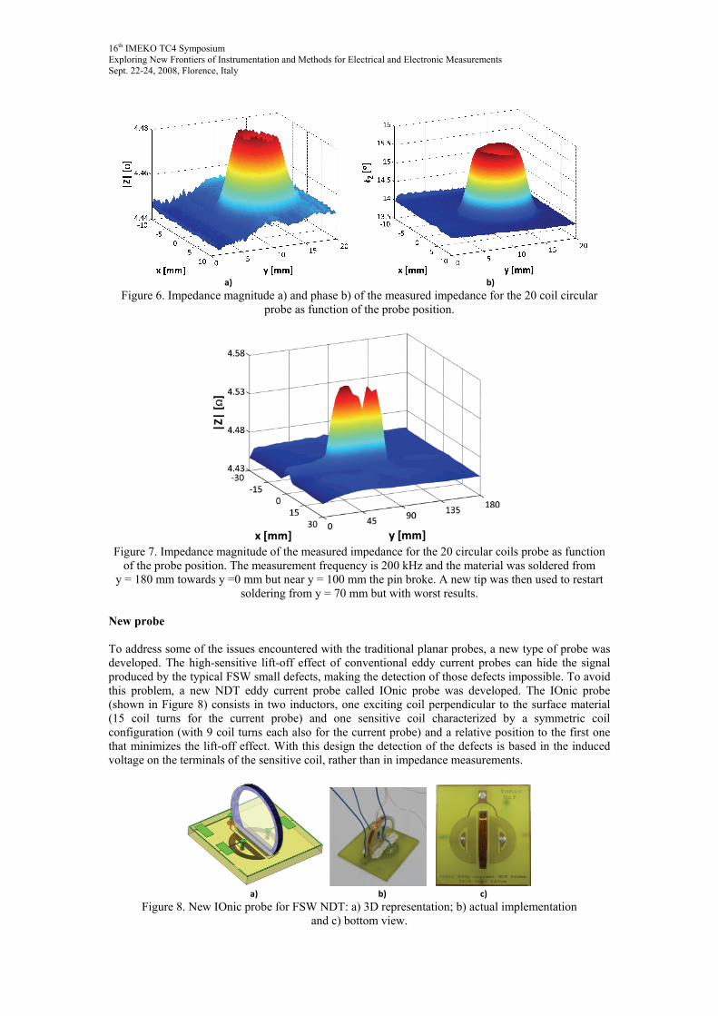
Frequency selection is a critical aspect of NDT. On one side, the measurement system is easier to develop and operate at lower frequencies, on the other hand there is an obvious sensitivity difference regarding lift-off and conductivity. In addition to these factors, different measurement frequencies correspond to different penetration depths which can be used to detect defects at different depths of the material. By using only the conductivity sensitivity criteria, the 20 circular coils probe should be used near 1.5 MHz. At this frequency, the penetration depth is around 75 μm. In the results that follow, frequency is set to 200 kHz in order to assess probe performance and impedance measurement range. In Figure 6, the impedance measurements corresponding to a 20×20 mm sweep with 0.5 mm resolution in both directions is shown. The material is AA2024 and it has a 3 mm diameter hole centred near x = 1 mm and y = 11.5 mm as is visible from the measured results. The results shown in Figure 7, depict the impedance magnitude measured on a real FSW (AA5083-H111 with 37.8 % IACS) with some defects. The results correspond to a 180 mm sweep in the y-axis with 5 mm steps and 60 mm sweep in the x-axis with 1 mm steps. The initial soldering was done at x = 0 mm from y = 180 mm towards y = 0 mm. However, near y = 100 mm, the pin broke and the welding had to be stopped. Welding resumed around y = 70 mm with a different tool and the welding parameters were incorrectly set which caused a defect along the joint. This defect is clearly seen in Figure 7 for x = 0 mm and y < 45 mm.
16th IMEKO TC4 Symposium Exploring New Frontiers of Instrumentation and Methods for Electrical and Electronic Measurements Sept. 22-24, 2008, Florence, Italy
a) b)
Figure 6. Impedance magnitude a) and phase b) of the measured impedance for the 20 coil circular probe as function of the probe position.
Figure 7. Impedance magnitude of the measured impedance for the 20 circular coils probe as function
of the probe position. The measurement frequency is 200 kHz and the material was soldered from y = 180 mm towards y =0 mm but near y = 100 mm the pin broke. A new tip was then used to restart
soldering from y = 70 mm but with worst results. New probe To address some of the issues encountered with the traditional planar probes, a new type of probe was developed. The high-sensitive lift-off effect of conventional eddy current probes can hide the signal produced by the typical FSW small defects, making the detection of those defects impossible. To avoid this problem, a new NDT eddy current probe called IOnic probe was developed. The IOnic probe (shown in Figure 8) consists in two inductors, one exciting coil perpendicular to the surface material (15 coil turns for the current probe) and one sensitive coil characterized by a symmetric coil configuration (with 9 coil turns each also for the current probe) and a relative position to the first one that minimizes the lift-off effect. With this design the detection of the defects is based in the induced voltage on the terminals of the sensitive coil, rather than in impedance measurements.
a) b) c)
Figure 8. New IOnic probe for FSW NDT: a) 3D representation; b) actual implementation and c) bottom view.

16th IMEKO TC4 Symposium Exploring New Frontiers of Instrumentation and Methods for Electrical and Electronic Measurements Sept. 22-24, 2008, Florence, Italy
With this new probe, the measurement procedure is different because the device is no longer an impedance whose value changes with the presence of defects. In the absence of defects the induced voltages in the two planar coils are the same and since their voltage is added in opposition, the total induced voltage is zero. To stimulate the excitation coil a sinewave generator (Agilent 33250A) is used and the current that is supplied to this coil is measured by the voltage across a 10 Ω precision resistor connected in series. The two voltages (the total induced voltage and the voltage across the reference resistor) are acquired by a 16-bit DAQ from National Instruments (NI USB-6251) operating at 500 kS/s with 10000 samples per channel and the ranges set at ±1 V for the voltage across the reference resistor and ±0.1 V for the induced total voltage. The measurement frequency was set to 1.6 MHz to maximize the amplitude fluctuations caused by a ramp defect with 300 μm width and 5.71º slope. Since this measurement frequency is well above the Nyquist frequency (250 kHz) aliasing occurs and the number of folds is used to correct the initial estimated signal frequency. In fact, the sampling rate of 500 kS/s was selected to try and assure that the measurement frequency would happen as far away as possible from the folds. At this sampling rate, the interchannel delay is 1 μs which has to be accounted for in order to estimate correctly the phase difference. The initial frequency estimative is done with the IpDFT [5]. Afterwards this apparent frequency is corrected (due to aliasing) and is sent to the seven-parameter sine-fitting [6] so that the amplitudes and phases of the two signals can be determined. In Figure 9, the real and imaginary components of the ratio between the induced voltage and excitation current are shown as a function of the probe position. For this figure, the x increment is 0.25 mm and the y increment is 1 mm. Notice that, near the ramp defect the measured probe output is similar to the measurements outside the ramp defect. This is caused by the fact that when the probe is centred in the defect, both induced voltages are identical and cancel themselves.
a) b) Figure 9. Real a) and imaginary b) components of the ratio between the induced voltage and excitation
current as measured with the IOnic Probe for the ramp defect described in the text.
To compare the sensitivity of the two types of probes, the measurement across the y dimension of a sequence of 300 μm cuts was done with both probes. The cuts are 20 mm apart with depths of 0.2 mm; 0.5 mm; 1 mm and 1.5 mm. After these single cuts there is a double cut with 1.5 mm and 1 mm with 2 mm separation. The normalized results, measured with the DAQ and the sine-fitting algorithms, are shown in Figure 10. Clearly the sensitivity of the IOnic probe is much bigger than that of the circular planar probe. Notice that, for the last set of cuts (the ones 2 mm apart and centred around 110 mm), the 20 circular coils planar probe shows absolutely no change from the variations it measured for the single cuts (it only has a larger amplitude than the 1.5 mm cut at around 90 mm). The IOnic probe, on the other hand shows a slight change in the variation profile that might be used to detect that it is not a simple cut like the previous ones. In fact, there is a pronounced asymmetry in the falling edges of both the real and imaginary components that is not present in the previous three cuts. Also noteworthy are the results for the first cut centred at 30 mm. For the IOnic probe, there is clearly a different measurement profile. This is caused by the reduced depth of this cut (0.2 mm) and the fact that some of the eddy currents are flowing underneath the actual cut. For 1.6 MHz the penetration depth is around 0.1 mm and so, at a depth of 0.2 mm there is still 13 % of the surface field. Note that, in Figure 9, this profile change is also present near the beginning of the ramp but is not so visible due to the axis limits and the selected point of view.

16th IMEKO TC4 Symposium Exploring New Frontiers of Instrumentation and Methods for Electrical and Electronic Measurements Sept. 22-24, 2008, Florence, Italy
a) b) Figure 10. Normalized (to the values at y = 0 mm) real and imaginary components of the ratio between
the induced voltage and excitation current as measured with the IOnic Probe a) and the 20 circular planar spiral coils probe b).
III. Conclusions
In this paper, a detailed comparison of planar eddy current probes for FSW of aluminium alloys is presented. Traditional planar probes have poor characteristics for the detection of defects in FSW due to the influence of lift-off and also because of their poor sensitivity to defects. The obtained results show that the analyzed planar probes are very sensitive to the lift-off and less sensitive to the material conductivity which is by itself an indication of defects in the friction stir welding process. The 20 circular coils probe was shown to be effective in detecting a 3 mm diameter hole (Figure 6). However, even in this extreme defect situation (not typically seen in FSW) the change in the impedance magnitude was only 0.6 % of the nominal value. To address some of the shortcomings of the traditional planar probes, a new probe called IOnic probe was developed. This probe has an excitation coil and two receiving coils in opposition. This configuration makes the probe less sensitive to lift-off as long as it is the same for both receiving coils. The two coils configuration also makes the probe more sensitive to defects because as soon as the probe nears a defect, a mismatch in the two voltages immediately appears and is detected by the probe. Sensitivity comparison measurements between the IOnic probe and the 20 circular coils planar probe demonstrate the large difference between them (Figure 10).
Acknowledgments The authors would like to acknowledge Fundação para a Ciência e a Tecnologia (FCT) for its financial support via: projects POCTI/EME/60990/2004 (acronym NDTStir), PTDC/EEA-ELC/72875/2006 and the PhD scholarship FCT – SFRH/BD/29004/2006.
References [1] Pedro Vilaça, Telmo Santos, Luisa Quintino, “Experimental analysis, defect evaluation and
computational developments of FSW”, Proceeding of IIW South East, Romania, 2006. [2] Telmo Santos, Bruno Silva, Pedro Vilaça, João Sousa, Luísa Quintino, “Fusão de dados em ensaios
não destrutivos utilizando decisão fuzzy para a avaliação de soldas obtidas pelo processo de fricção linear”, Soldagem e Inspecção, vol. 12, n. 3, pp. 179-187, 2007 (in portuguese).
[3] R. Ditchburn, S. Burke, “Planar rectangular spiral coils in eddy-current nondestructive Inspection”, NDT&E International, vol. 38, n. 8, pp. 690-700, 2005.
[4] Agilent 4294A Precision Impedance Analyzer, Operation Manual and Programming Manual, Agilent Technologies.
[5] H. Renders, J. Schoukens, G. Vilain, “High-accuracy spectrum analysis of sampled discrete frequency signals by analytical leakage compensation,” IEEE Trans. Instr. Meas., vol. 33, no. 4, pp. 287–292, Dec 1984.
[6] Pedro M. Ramos and A. Cruz Serra, “A new sine-fitting algorithm for accurate amplitude and phase measurements in two channel acquisition systems”, Measurement, Elsevier, Vol. 41, No. 2, pp. 135-143, Feb. 2008.