template-assisted synthesis and study of one …
TRANSCRIPT

TEMPLATE-ASSISTED SYNTHESIS AND STUDY OF
ONE-DIMENSIONAL NANOSTRUCTURES ARRAY
LOH PUI YEE
B. Sc. (Hons.), NUS
A THESIS SUBMITTED
FOR THE DEGREE OF DOCTOR OF PHILOSOPHY
DEPARTMENT OF CHEMISTRY
NATIONAL UNIVERSITY OF SINGAPORE
2013


i
Acknowledgements
I would like to express my deepest gratitude to the people who had helped
me through this path less travelled and made this thesis possible.
Firstly, for my PhD supervisor, Associate Professor Chin Wee Shong, who
always find time for me despite her busy schedule. I would like to thank her
for her professional guidance, enthusiastic encouragement and useful
critiques. No matter it was for work or personal matters, she has been of
good counsel and support.
Another big thanks to my co-supervisor, Associate Professor Sow Chorng
Haur, for all the encouragement and productive discussions. His speedy
proof-reading and constructive comments for paper writing are also very
much appreciated.
Special thanks to Mr. Ho Yeow Lin Peter and Ms. Ng Yuting, final year
undergraduate students under my supervision, for their respective
preliminary work on MWCNT/PPV core-shell nanowires and Co/Al-LDH
nanostructures which allowed me to further optimize the synthesis
parameters and study their properties. Thanks to Mr. Lee Kian Keat as well
for sharing his knowledge on electrochemical capacitors and sensors.

Acknowledgements
ii
Many thanks to Ms. Lim Xiaodai Sharon for her kind support in the
synthesis of aligned MWCNT arrays and the usage of focused laser beam
systems in A/P Sow Chorng Haur’s laboratory. Also, thanks to Mr. Ho Kok
Wen and Mr. Lee Ka Yau for their assistance regarding the SEM and EDX
instruments; Dr. Zhang Jixuan and Mr. Henche Kuan in the Department of
Materials Science and Engineering for their support in TEM and XPS usage;
Mr. Teo Hoon Hwee and Ms. See Sin Yin for their guidance in DR-FTIR
measurement; and Mdm Tan Teng Jar for her support in the XRD
measurement.
I am also very grateful to my seniors, Dr. Xu Hairuo and Dr. Yin Fenfang
for their professional guidance and personal encouragement. Thanks also
go to all my group members, Dr. Teo Tingting Sharon, Ms. Tan Zhi Yi, Mr.
Lee Kian Keat, Mr. Huang Baoshi Barry, Ms. Yong Wei Ying Doreen, Ms.
Chi Hong and Mr. Chen Jiaxin, for their support and making my days in the
laboratory always enjoyable.
I am also thankful for the research scholarship provided by National
University of Singapore (NUS).
Finally, my heartfelt gratitude goes to my family and my loving husband
for their unconditional love and encouragement.

iii
Table of Contents
Summary ………………………………………………………………
List of Publications ……………………………………………….…...
List of Tables ………………………………………………………….
List of Figures …………………………………………………………
List of Abbreviations ………………………………………………….
Chapter 1 Introduction
1.1 One-dimensional (1D) nanostructures …………………..
1.1.1 Single-component NWs and NTs ……………….
1.1.2 Multi-component NWs and NTs ………….…….
1.2 Strategies for the synthesis of 1D nanostructures ……….
1.2.1 Vapour-liquid-solid (VLS) and Solution-liquid-
solid (SLS) methods …………………………….
1.2.2 Kinetic-controlled growth methods …………….
1.2.3 Template-assisted methods ……………………...
1.3 Objective and scope of thesis …………………………...
1.4 References ………………………………………………
Chapter 2 Experimental
2.1 List of chemicals and reagents …………………………..
2.2 Synthesis of 1D nanostructures using AAO as template...
viii
xi
xiii
xiv
xxi
1
2
3
4
6
8
12
13
18
21
33
33
34

Table of contents
iv
2.2.1 Synthesis of PPV 1D nanostructures ……………
2.2.2 Electrodeposition of polypyrrole and metallic
components for core-shell 1D nanostructures ….
2.2.3 Synthesis of Co/Al layered double hydroxides
hierarchical 1D nanostructures ………………….
2.3 Synthesis of 1D nanostructures using aligned MWCNT
as template ………………………………………………
2.3.1 Synthesis of aligned MWCNT arrays …………..
2.3.2 Synthesis of aligned MWCNT/PPV core-shell
nanowires ………………………………………..
2.4 Micro-patterning of PPV 1D nanostructures array via
laser pruning technique ………………………………….
2.5 Oxygen reactive ion etching (O2 RIE) and heat
treatment of core-shell nanostructures …………………..
2.6 Measurement of electrochemical capacitance of Co/Al
layered double hydroxides hierarchical 1D
nanostructures …………………………………………...
2.7 Measurement of electrochemical glucose sensing of
Co/Al layered double hydroxides hierarchical 1D
nanostructures …………………………………………...
2.8 Measurement of photocurrent response of aligned
MWCNT/PPV core-shell nanowires ……………………
2.9 Characterization techniques ……………………………..
35
36
37
38
39
40
41
42
43
44
45
46

Table of Contents
v
2.9.1 Scanning Electron Microscopy (SEM) …………
2.9.2 Transmission Electron Microscope (TEM) and
High Resolution TEM (HRTEM) ……………….
2.9.3 Energy Dispersive X-ray Spectroscopy (EDX) …
2.9.4 Diffuse Reflectance Fourier-Transform Infrared
(DR-FTIR) ………………………………………
2.9.5 Raman Scattering Spectroscopy ………………...
2.9.6 UV-Visible Absorption Spectroscopy …………..
2.9.7 Photoluminescence (PL) Spectroscopy …………
2.9.8 Fluorescence Microscopy (FM) …………………
2.9.9 X-ray Diffraction (XRD) ………………………..
2.9.10 X-ray Photoelectron Spectroscopy (XPS) ………
2.10 References ………………………………………………
Chapter 3 Fabrication and Micro-Patterning of Luminescent
Poly(p-phenylene vinylene) Nanowire and Nanotube
Arrays
3.1 PPV 1D nanostructures ………………………………….
3.1.1 Effects of oxygen and moisture in the plating
solution ………………………………………….
3.1.2 Effects of applied potential ……………………...
3.1.3 Characterization of PPV nanostructures ………..
3.2 Micro-patterning of PPV nanostructures array via laser
pruning technique ……………………………………….
46
47
48
48
48
49
49
49
50
50
50
53
55
56
60
63
67

Table of contents
vi
3.2.1 Laser pruning of PPV nanostructure arrays ……..
3.2.2 Optical properties of laser-modified PPV arrays...
3.2.3 Effect of focused laser beam on PPV NTs arrays..
3.3 Summary ………………………………………………...
3.4 References ………………………………………………
Chapter 4 Synthesis of Controllable Core-shell Nanostructures
via Pore Widening Method
4.1 Synthesis and characterizations of core-shell
nanostructures …………………………………………...
4.1.1 Polymer/metal core-shell nanowires …………….
4.1.2 Metal/metal core-shell nanowires ……………….
4.1.3 Multi-layered nanowires ………………………...
4.1.4 Multi-layered nanotubes ………………………...
4.2 Summary ………………………………………………...
4.3 References ………………………………………………
Chapter 5 Synthesis and Electrochemical Properties of
Cobalt/Aluminium Layered Double Hydroxides
Hierarchical Nanostructures
5.1 Synthesis and characterizations of Co/Al-LDH
hierarchical nanostructures ……………………………...
5.2 Electrochemical capacitance of Co/Al-LDH hierarchical
nanostructures …………………………………………...
67
69
71
85
86
91
93
95
100
102
106
109
110
113
118
124

Table of Contents
vii
5.3 Electrochemical glucose sensing of Co/Al-LDH
hierarchical nanostructures ……………………………...
5.4 Summary ………………………………………………...
5.5 References ………………………………………………
Chapter 6 Synthesis and Photocurrent Study of Aligned
MWCNT/PPV Core-shell Nanowires
6.1 Synthesis and characterizations of aligned
MWCNT/PPV core-shell nanowires ……………………
6.2 Optical properties of aligned MWCNT/PPV core-shell
nanowires ………………………………………………..
6.3 Photocurrent response of aligned MWCNT/PPV core-
shell nanowires ………………………………………….
6.4 Summary ………………………………………………...
6.5 References ………………………………………………
Chapter 7 Conclusions and Outlook
131
142
143
149
151
159
162
169
170
175

viii
Summary
The ability to control the length and shell thickness in synthesis of multi-
layered one-dimensional (1D) nanostructures is an important aspect in the
exploration of their properties, leading to the realization of their potential
applications. Template-assisted synthesis using anodic aluminium oxide
(AAO) membrane as sacrificial template and aligned multi-walled carbon
nanotubes (MWCNT) as deposition surface are two versatile methods to
grow 1D nanostructures. Thus, this thesis further demonstrates a few
approaches of using the templates together with electrochemical and some
chemical methods to grow various 1D hetero-nanostructures. Some
potential applications of the resultant nanostructures are also illustrated.
To begin, Chapter 1 gives an overall background and scopes of this
thesis. Chapter 2 then describes all necessary experimental procedures for
syntheses, characterizations and properties measurements of nanostructures
obtained.
In Chapter 3, we established optimal parameters to electropolymerize
poly(p-phenylene vinylene) (PPV) into AAO nanochannels to give
luminescent organic 1D nanostructures. Nanowires (NWs) and nanotubes
(NTs) can be prepared by manipulating the conditions of plating solution
and deposition potential, while their length is controllable by the deposition
time. Micro-patterning via focused laser beam was also demonstrated. An
interesting “red-shifting” of the photoluminescence maxima was observed
upon laser modification in air but not in inert environment.

Summary
ix
To further demonstrate the versatility of AAO, Chapter 4 presents our
Pore-Widening method in creating coaxial multi-layered 1D hetero-
nanostructures. Nanochannels of AAO have a certain thickness which can
be manipulated with controlled etching to create annular gap around the
cores for subsequent deposition of shells. With judicious selection of
materials and sequences of steps, a few strategies are illustrated, leading to
fabrication of various hetero-nanostructures such as polymer/metal,
metal/metal, polymer/metal/metal and metal oxide/metal core-shell
nanostructures.
AAO can be more than just a sacrificial template for deposition of 1D
nanostructures. In Chapter 5, AAO was employed to fabricate cobalt-
aluminium layered double hydroxides (Co/Al-LDH) hierarchical
nanostructures. Here, AAO not only acts as template, but also provides Al3+
ions in the alkaline solution that isomorphously substitute some of the Co2+
during the hydroxide formation, forming Co/Al-LDH NFs on Co NWs.
These arrays can be directly used as electrode for electrochemical capacitor
and glucose sensing applications. Effects of alkaline treatment time on the
morphology, Al content and properties of LDH NFs will also be discussed.
In the last result chapter, Chapter 6 describes the use of aligned
MWCNT as support for growth of 1D nanostructures. Here, the
electropolymerization conditions established in Chapter 3 is utilized to
coaxially grow PPV onto the MWCNT, forming arrays of MWCNT/PPV
core-shell nanostructures. Comparing to constant potentiometry, pulsed
potentiometry was found to show better control of the shell thickness. The

Summary
x
resulting nanostructures were then tested for photocurrent response towards
405 nm laser.
Lastly, Chapter 7 gives an overall conclusion of the thesis work. Some
future outlook and further exploration are also proposed here.

xi
List of Publications
Nanowires with Controllable Core-Shell Structures: A “Pore Widening”
Method. P. Y. Loh, C. M. Liu, C. H. Sow, W. S. Chin. RSC Adv. 4 (2014)
8735-8740.
CoOOH Nanosheet Electrodes: Simple Fabrication for Sensitive
Electrochemical Sensing of Hydrogen Peroxide and Hydrazine. K. K.
Lee, P. Y. Loh, C. H. Sow, W. S. Chin. Biosens. Bioelectron. 39 (2013)
255-260.
CoOOH Nanosheets on Cobalt Substrate as a Non-enzymatic Glucose
Sensor. K. K. Lee, P. Y. Loh, C. H. Sow, W. S. Chin. Electrochem.
Commun. 20 (2012) 128-132.
Facile Fabrication of One-dimensional Multi-component
Nanostructures using Porous Anodized Alumina Membrane. P. Y. Loh,
C. M. Liu, W. C. Pua, F. Y. Kam, W. S. Chin. Cosmos 6 (2010) 221-234.
Fabrication and Micropatterning of Luminescent Poly(p-phenylene
vinylene) Nanotube Arrays. P. Y. Loh, C. M. Liu, C. H. Sow, W. S. Chin.
– manuscript in progress.

List of Publications
xii
Co/Al Layered Double Hydroxides Hierarchical Nanostructures: A
Binderless Electrode for Electrochemical Capacitor. P. Y. Loh, K. K.
Lee, Y. Ng, C. H. Sow, W. S. Chin. – manuscript submitted for publication.
Co/Al Layered Double Hydroxides Hierarchical Nanostructures as a
Sensitive Non-enzymatic Glucose sensor. P. Y. Loh, K. K. Lee, Y. Ng, C.
H. Sow, W. S. Chin. – manuscript in progress.

xiii
List of Tables
Table Page
2.1: Chemicals and solvents used in the work described in this thesis.
3.1: Assignments of the observed vibrational bands of PPV.26
3.2: Peak areas for all fitted components of C 1s and O 1s XPS spectra as shown in Figure 3.12. Data were normalized by respective atomic sensitivity factor (ASF) and number of scans.
3.3: Energy provided by laser spot and energy absorbed by PPV NTs at the specified wavelengths.
5.1: Average atomic percentage obtained from EDX analyses of Co/Al-LDH samples for each alkaline treatment time.
5.2: Examples of Co/Al-LDH-based electrodes reported in the literatures and their EC performances.
5.3: A comparison of non-enzymatic Glc sensing performance of Co-based electrodes in the literature.
6.1: PPV shell thickness estimated from TEM analysis, PC amplitude (Jp-J0), and two characteristic time constants (τ1 and τ2) of PC build-up and decay, at bias 0.10 V for samples prepared at the corresponding PPV deposition pulse time.
33
65
77
84
122
130
138
167

xiv
List of Figures
Figure Page
1.1: Strategies to fabricate 1D nanostructures: (A) dictation by the intrinsic anisotropic crystallographic structure, (B) directed growth by a liquid droplet as in the vapour-liquid-solid (VLS) and solution-liquid-solid (SLS) processes, (C) kinetic control by capping reagent, and (D) template-assisted growth. [Schematics redrawn and adapted from Ref. 51]
1.2: Schematic showing the mechanism for growth of NWs via VLS method. [Schematics redrawn and adapted from Ref. 53]
1.3: Schematic showing the mechanism for growth of NWs via SLS method. [Schematics redrawn and adapted from Ref. 53]
1.4: Schematic diagram showing the formation of NWs, NTs and multi-component nanostructures by complete, incomplete and sequential filling of the nanochannels of AAO, respectively.
1.5: Schematic diagram illustrating the formation of NWs and NTs by templating against the cylindrical micelles or inverse micelles, respectively. [Schematics redrawn and adapted from Ref. 51]
2.1: Three-electrode configuration setup for electrochemical
deposition of nanostructures and measurements of electrochemical properties.
2.2: Schematic diagram for the synthesis of PPV 1D nanostructures by electrodeposition using AAO as template.
2.3: Schematic diagram for the fabrication of Co/Al-LDH hierarchical nanostructures using AAO as template and source of Al3+ ions.
2.4: Schematic diagram for the growth of MWCNT/PPV core-shell nanostuctures on n-type Si via PECVD followed by electrochemical method.
7 9
11
15
17
35
36
38
39

List of Figures
xv
2.5: Schematic of the optical microscope-focused laser beam system used for micro-patterning. For laser pruning in air, samples were placed directly under the laser beam as shown in the bottom left box; while the box in the bottom right shows the chamber for laser pruning in vacuum or helium environment.
2.6: Schematic diagram for the measurement of I-V and PC response of MWCNT and MWCNT/PPV core-shell NWs.
3.1: The mechanism for electrochemical polymerization of PPV from TBX as proposed by Kim et al.18
3.2: SEM images of PPV NWs electrodeposited at -2.34 V for cathodic charge of (A) 0.26 C, (B) 0.5 C, (C) 1.0 C and (D) 2.0 C. Insets show the side-view of the NWs. (E) A plot of the length of PPV NWs synthesized as a function of charge deposited. The line is drawn as a guide.
3.3: SEM images of PPV NTs electrodeposited at -2.34 V using distilled ACN plating solution for cathodic charge of (A) 0.26 C and (B) 2.0 C. The insets show side-view of the NTs. TEM images of PPV NTs prepared for cathodic charge of (C) 0.26 C and (D) 1.0 C. (E) A plot of the length of PPV NTs synthesized as a function of charge deposited.
3.4: TEM images of PPV nanostructures electrodeposited from (A-C) as-received and (D-E) distilled ACN plating solutions for cathodic charge of 1.0 C at the potentials specified. (F) Plot of tubular portion versus applied cathodic potential.
3.5: Representative (A) DR-FTIR and (B) Raman spectra of PPV NWs and NTs, with the characteristic FTIR and Raman peaks of PPV as labelled.26 Detailed assignment is given in Table 3.1. Raman spectra were displaced for ease of comparison.
3.6: UV-visible absorption and PL spectra of PPV NWs and PPV NTs arrays. (Excitation wavelength for PL: 325 nm)
3.7: SEM images of patterns and areas cut using 40mW focused red laser for (A) PPV NWs array and (B) PPV NTs array. Top panels show top views of the laser-pruned patterns. The alphabets “NUS” are the uncut arrays while the surrounding square areas were cut away. Bottom panels show tilted views of the nanostructures areas after laser pruning.
42
45
55
57
59
62
64
66
68

List of Figures
xvi
3.8: PL spectra of (A) PPV NWs and (B) PPV NTs arrays, as-grown and laser-modified (at power 20, 30 and 40 mW) in air, vacuum and helium by focused red laser. (Excitation wavelength: 325 nm)
3.9: Fluorescence microscopic images of patterns cut on (A) PPV NWs array and (B) PPV NTs arrays using 40 mW red laser (660 nm) in air, vacuum and helium environment.
3.10: (A) DR-FTIR and (B) Raman spectra of PPV NTs, as-grown and laser-modified in air and vacuum by focused red laser.
3.11: XPS spectra for (A) Br 3d, (B) C 1s and (C) O 1s binding energy for PPV NTs, as-grown and after laser pruning in air and vacuum using focused red laser. All spectra are normalized with their integral intensities calibrated to unity and offset for ease of comparison.
3.12: XPS spectra for C 1s and O 1s of PPV NTs: (A), (B) as-grown, (C), (D) modified in air using 30 mW focused red laser.
3.13: Effect of laser power used for patterning on the (A) FTIR peak area ratio of 1695 cm-1 to 1512 cm-1, (B) XPS peak area ratio of O 1s to C 1s peaks and (C) PL maxima of PPV NTs, for samples treated in air and in vacuum. Excitation wavelength for PL: 325 nm.
3.14: (A) UV-visible absorption spectra, (B) DR-FTIR spectra and (C) PL spectra of PPV NTs array before and after global blue laser (405 nm, unfocused) irradiation in air and vacuum. Excitation wavelength for PL: 325 nm.
3.15: (A) PL and (B) DR-FTIR spectra of PPV NTs, as-grown and laser-modified in air and vacuum by focused green laser. (Excitation wavelength for PL: 325 nm)
4.1: Schematic of the “Pore Widening” steps to generate (A)
polymer/metal and (B) metal/metal (M1/M2) core-shell nanostructures.
4.2: (A) SEM image of as-grown PPy NWs array and (B) graph
of length of PPy NWs as a function of charge deposited.
4.3: Side (A and B) and top view (C and D) SEM images of the PPy/Ni core-shell NWs prepared after pore widening for 1 hour (A, C) and 2 hours (B, D), respectively.
70
71
73
75
77
79
80
82
94
95
97

List of Figures
xvii
4.4: (A, B) Top view SEM images of the core-shell PPy/Ni NWs
prepared at pore-widening time of (A) 1 hour and (B) 2 hours after exposure to oxygen reactive ion etching for 15 minutes. (C) Graph of Ni shell thickness as function of pore-widening time. (D) Side view SEM image of PPy/Cu core-shell NWs array.
4.5: Analysis of PPy/Ni core-shell NWs shown in Figure 4.3A after heat treatment at 400°C in air for 3 hours. (A) Top view SEM image, and (B) a comparison of the EDX spectra before and after the heat treatment.
4.6: Cu/Ni core-shell NWs array prepared using the “Pore Widening” method. The EDX spectra on the right were taken at three different locations marked as a, b and c on the SEM image on the left.
4.7: Schematic of the growth mechanism of (A) polymer/metal and (B) metal/metal core-shell NWs in a single nanochannel of AAO template.
4.8: Schematic of further “Pore Widening” strategy for synthesis of polymer/metal/metal tri-layered core-shell NWs by repeating steps depicted in Figure 4.1.
4.9: SEM image of PPy/Cu/Ni tri-layer core-shell NWs.
4.10: EDX line analysis of the tri-layered NWs: (A) SEM image of the PPy/Cu/Ni tri-layered core-shell NWs array and (B) the compositional line profiles probed by EDX along the red line in (A), showing well-correlated Ni and Cu signals along the NW axis.
4.11: Schematic procedures for the synthesis of metal oxide/metal DWNT.
4.12: SEM image showing CuxO/Ni DWNT.
4.13: EDX line analysis of the CuxO/Ni DWNT, indicating a fairly uniform distribution of the metal and oxide.
5.1: General structure of a layered double hydroxide (LDH),
with several parameters as defined. [Schematics redrawn and adapted from Ref. 1, 6]
98
100
101
102
103
104
105
106
107
108
114

List of Figures
xviii
5.2: Average length of Co NWs obtained as a function of electrodeposition duration.
5.3: SEM images of Co/Al-LDH samples after alkaline treatment for (A) 1, (B) 18, (C) 24 and (D) 48 hours. The left and right panels show respectively the side and top views for each samples.
5.4: XRD pattern of Co/Al-LDH samples prepared at the specified alkaline treatment time. Characteristic peaks for Co/Al-LDH are as labelled. Reference peaks: Au (JCPDS 01-071-4614), Co (JCPDS 01-071-4652), Cu (JCPDS 01-071-4611) and Co6Al2CO3(OH)16.4H2O (JCPDS 00-051-0045).
5.5: CV curves at scan rate of 10 mV/s for Co/Al-NWNF electrodes in 1 M KOH electrolyte. Samples prepared at varying alkaline treatment time are compared.
5.6: C-D curves at 2.5 mA/cm2 current density for Co/Al-NWNF electrodes in 1 M KOH electrolyte. Samples prepared at varying alkaline treatment time are compared.
5.7: Correlation for Al content and area-specific capacitance at varying current densities against alkaline treatment time.
5.8: Coulombic efficiency against current density for samples at varying alkaline treatment time. Inset: cycle life data at 12.7 mA/cm2.
5.9: (A) CV curves at 10 mV/s in the absence and increasing amount of glucose (Glc) in 0.1 M NaOH solution. Dashed and solid lines are for Co/Al-NWNF-1 and Co/Al-NWNF-24 samples, respectively. (B) A cartoon showing the electrooxidation of glucose on Co/Al-LDH NFs grown on Co NWs.
5.10: Amperometric response upon the successive addition of Glc in 0.1 M NaOH at the respective applied potential for Co/Al-NWNF-1 and Co/Al-NWNF-24. Inset: The corresponding calibration curves. [Note: The dilution effect has been taken into consideration for all concentration values indicated]
5.11: Expanded region of linear range from the calibration curve
in the inset of Figure 5.10.
119
120
123
125
126
128
129
133
135
136

List of Figures
xix
5.12: Amperometric response of Co/Al-NWNF electrodes to 4 mM Glc at 0.3 V in electrolytes of varying NaOH concentration and pH values.
5.13: Amperometric response of Co/Al-NWNF electrodes to 4 mM Glc at 0.3 V in the presence of interfering compounds (UA: uric acid, AA: ascorbic acid) in 0.1 M NaOH electrolyte.
6.1: (A) Low and (B) high magnification of side view SEM images of aligned MWCNT arrays as-grown via PECVD.
6.2: SEM images of MWCNT/PPV obtained via electrodeposition at constant potential of -2.34 V for total charge of 0.5 C at (A) low and (B) high magnification. The white box in (A) indicates area where image (B) was obtained.
6.3: Profile of pulse potential used to electrodeposit PPV onto MWCNT. Shown here are two of the pulse cycles that are repeated to achieve specific duration of deposition.
6.4: Representative SEM images of (A) MWCNT, (B) MWCNT/PPV-10, (C) MWCNT/PPV-20 and (D) MWCNT/PPV-30. The last two numbers in sample labels denote the total duration of the pulse cycles shown in Figure 6.3.
6.5: HRTEM images of (A) MWCNT, (B) MWCNT/PPV-10, (C) MWCNT/PPV-20 and (D) MWCNT/PPV-30. (E) Graph of PPV shell thickness obtained as a function of total pulse time.
6.6: Raman spectra of MWCNT and MWCNT/PPV core-shell NWs electrodeposited at varying pulse durations as indicated. Excitation wavelengths are (A) 785 nm, (B) 633 nm and (C) 532 nm, respectively. D and G bands of MWCNT are indicated in all spectra while characteristic peaks of PPV are indicated in (C).
6.7: Typical UV-visible absorption spectra of MWCNT and MWCNT/PPV-30. The reflectance was normalized such that the mean intensity over all the data points is unity.
139
141
152
153
154
155
156
158
160

List of Figures
xx
6.8: PL spectra of MWCNT and MWCNT/PPV electrodeposited at varying pulse durations as indicated. The PL intensities were normalized such that the mean intensity over all the data points is unity.
6.9: Current density versus potential (J-V) curves of MWCNT and MWCNT/PPV core-shell NWs prepared at the specified pulse times. J-V for double-sided tape is included for comparison.
6.10: Photocurrent (PC) time response of MWCNT and MWCNT/PPV core-shell NWs prepared at indicated pulse durations at bias voltage of 0.1 V. PC for double-sided tape is included for comparison.
6.11: (A) Rising and (B) decay photocurrent time response of MWCNT/PPV-20 at bias voltage of 0.10V upon light “on” and light “off” state, respectively. The black solid lines are the exponential fittings of the corresponding data in gray. Inset boxes show the calculated parameters for each fit.
161
163
164
166

xxi
List of Abbreviations
λexc Excitation wavelength
0D Zero-dimensional
1D One-dimensional
2D Two-dimensional
3D Three-dimensional
AA L-Ascorbic acid
AAO Anodic aluminium oxide
ACN Acetonitrile
ALD Atomic layer deposition
ASF Atomic sensitivity factor
C-D Charge-discharge
CE Counter electrode
CMC Critical micelle concentration
CNT Carbon nanotubes
Co/Al-LDH Cobalt-aluminium layered double hydroxides
Co/Al-NWNF-y Label for “Co/Al-LDH NFs on Co NWs” electrodes,
with y being the hours of alkaline treatment time
during sample preparation
CPs Conducting polymers
CV Cyclic voltammetry
CVD Chemical vapour deposition

List of Abbreviations
xxii
DR-FTIR Diffuse Reflectance Fourier-Transform Infrared
Spectroscopy
DSSC Dye-sensitized solar cells
DWNT Double-walled nanotubes
ECs Electrochemical capacitors
EDLCs Electric double-layer capacitors
EDX Energy Dispersive X-ray Spectroscopy
ESs Electrochemical sensors
Et4NBF4 Tetraethylammonium tetrafluoroborate
EtOH Ethanol
FET Field-effect transistor
FIB Focused ion-beam
FM Fluorescence Microscopy
Glc Glucose
GOx Glucose oxidase
HRTEM High-Resolution Transmission Electron Microscope
HT Hydrotalcite
IEP Isoelectric point
ITO Indium tin oxide
I-V Current-voltage
J-V Current density-voltage
KOH Potassium Hydroxide
LDH Layered double hydroxides

List of Abbreviations
xxiii
LOD Limit of detection
LOL Limit of linearity
M1 First metal component
M2 Second metal component
MWCNT Multi-walled carbon nanotubes
MWCNT/PPV-n Label for samples of MWCNT/PPV core-shell NWs,
where n is the total duration of the overall pulse cycles
in minutes
NaOH Sodium hydroxide
NFs Nanoflakes
NPs Nanoparticles
NRs Nanorods
NSs Nanosheets
NTs Nanotubes
NWs Nanowires
O2 RIE Oxygen reactive ion etching
OPVs Oligophenylene vinylenes
PA Polyacetylene
PANI Polyaniline
PC Photocurrent
PCB Printed circuit board
PECVD Plasma-enhanced chemical vapour deposition
PL Photoluminescence Spectroscopy
List of Abbreviations
xxiv
PPV Poly(p-phenylene vinylene)
PPy Polypyrrole
PTh Polythiophene
RE Reference electrode
RF Radio frequency
rpm Revolutions per minute
RSD Relative standard deviation
sccm Standard cubic centimeter per minute
SEM Scanning Electron Microscope
SLS Solution-liquid-solid
TBX α,α,α’,α’-tetrabromo-p-xylene
TEM Transmission Electron Microscope
TFTs Thin-film transistors
UA Uric acid
VLS Vapour-liquid-solid
WE Working electrode
XPS X-ray Photoelectron Spectroscopy
XRD X-ray Diffraction

1
Chapter 1
Introduction
Nanotechnology involves the manipulation of matters with at least one
dimension sized between 1 to 100 nm. The design and exploitation of such
nanomaterials have attracted numerous research interests, both for
fundamental studies and industrial applications.1-4 This is due to their new
or enhanced size- and shape-dependent properties as compared to their bulk
counterparts. The reduction in sizes can lead to quantum confinement of
electrons which was shown to influence the electrical conductivity and
magnetic susceptibility of these materials.5-8 Besides, their higher surface
area and catalytic properties also proved to be useful for applications in
electrochemical sensors and capacitors.1,4 With the invention and
development of advanced measuring instrumentation, scientists have been
able to “see” and “manipulate” structure on the nanometer region. Such
technological advancement further encourages the research of
nanomaterials for a broader and ever increasing range of applications.
As proposed by Pokropivny et al.,9 nanostructures can be classified
according to their dimensionality as a whole, that is zero-dimensional (0D),
one-dimensional (1D), two-dimensional (2D) and three-dimensional (3D).
0D nanostructures have all three dimensions that are sized in nanometric
size range. Examples are quantum dots, nanoparticles (NPs) and hollow
nanospheres.10-12 As for 1D nanostructures, one of the dimensions is

Chapter 1
2
outside of nanometer range with examples such as nanoribbons, nanobelts,
nanorods (NRs), nanowires (NWs) and nanotubes (NTs).13-17 2D
nanostructures are such as nanoprisms, nanoplates, nanosheets, nanowalls
and nanodisks, with two dimensions outside of nanometer range.18-21 3D
nanostructures are assemblies or combinations of various nanostructures
such as dendritic nanoballs, nanocoils, nanoflowers and branched NWs.22-25
Among these nanostructures, 1D NWs and NTs are the focus of this thesis
work and will be discussed in more details in the following sections.
1.1 One-dimensional (1D) nanostructures
Since the discovery of carbon nanotubes (CNT) in 1991,26 research
interests towards 1D nanostructures have increased tremendously. With
their unique properties and increased surface area arises from their high
aspect ratio (length-to-width), 1D nanostructures have demonstrated
immense potentials both as the active functional materials2-4 or as
interconnects for various nanoscale devices.27-29 As mentioned above, there
are many forms of 1D nanostructures, all of which are characterized by a
high aspect ratio. The most common ones are NRs, NWs and NTs. The
only difference between NWs and NRs is their aspect ratio which is often
defined as more and less than 20 for NWs and NRs, respectively. Their
properties are largely dependent on the type of material but may also be
affected by the shape, morphology and structure (i.e. crystalline or
amorphous).

Chapter 1
3
1.1.1 Single-component NWs and NTs
Single-component 1D nanostructures are simply NWs and NTs that
consist of one type of material. The applications of such nanostructures are
mainly dependent on the properties of material and/or the increased surface
area of the nanostructures. Depending on the material that forms the single-
component NWs or NTs, they can be applied as active functional electrodes
or as interconnects in nanoscale devices.
One example of application as an electrode is the usage of V2O5 NWs
array as cathode for lithium (Li) ion battery.30 With decreased diameter of
the electrode material, the distance that Li+ ion must diffuse within the
electrode would be decreased which then improves the low-temperature
performance of Li ion batteries. This opens up potential utilization of
lithium ion batteries under sub-zero temperatures. In addition, magnetite
Fe3O4 NWs31 and hydrogen-treated cap-opened Si NTs32 also exhibit
excellent performance as anodes for Li-ion battery. Array of 1D metal
oxides nanostructures are also popularly studied as photoelectrodes for dye-
sensitized solar cells (DSSC), especially TiO2 and ZnO NWs and NTs.3
These 1D photoelectrodes were shown to improve charge transfer by
providing direct pathways for electron transport in the device as compared
to NPs films.
Other than the inorganic components, conducting polymer NWs such as
polyaniline (PANI) also demonstrated various useful applications such as
chemical sensors, supercapacitors33 and biosensor.34 Polypyrrole (PPy)

Chapter 1
4
NWs array also exhibited excellent response to pH changes and good
stability over time.35
Recently, an interesting work presented the fabrication of ultra-long Cu
NWs array bumps as “Velcro” interconnects to connect circuits on two
different substrates.28 These arrays were deposited onto conductive
electrode on both Si die and printed circuit board (PCB) substrates. By
attaching these NWs arrays, they form a contact similar to the commercial
“Velcro” type loop fastener.
1.1.2 Multi-component NWs and NTs
It is only natural to progress from single-component towards the
fabrication and design of more complex, multi-component 1D
nanostructures for wider range of applications. In addition to the benefits of
1D morphology, the coupling of different materials into a 1D nanostructure
also presents multi-functionality or new properties arising from synergistic
effects between the different material components, such as p-n junctions or
Schottky diodes. Examples of such nanostructures include segmented NWs,
core-shell NWs and multi-walled NTs, all of which contain hetero-
junctions between various combinations of materials.
Various segmented NWs consisting of metal and conducting polymer
(CP) were fabricated.36 An example is Co-PPy-Co NWs which were
fabricated electrochemically in single-wire form inside the anodic
aluminium oxide (AAO) template.37 Using this metal-CP-metal NW, a
field-effect transistor (FET) was easily produced, simply by patterning a

Chapter 1
5
gate on one side of the wire. The advantages of this in-wire FET include
reproducible metal-organic junctions, controllability of the diameter and
easy integration of the devices. Rather than only a few segments, multi-
segmented NWs were also fabricated such as Ni-Cu and Ni-Pt multi-
segmented NWs arrays.38, 39 These NWs were fabricated in AAO template
using pulsed electrochemical method from a single plating solution
consisting of both metal ions. Both arrays showed enhanced coercivity than
that of the bulk and NWs of Ni, and this can be attributed to single
magnetic domain of cylindrical Ni nanoparticles separated by Cu or Pt
segments.
Core-shell NWs and NTs with coupled core and shell materials have
shown great potential applications in solar cells, sensors and energy
storage.16, 40-43 Various combinations of materials were explored including
semiconductors, metals, metal oxides and conductive polymers.40, 42-48
Some of these hetero-nanostructured architecture reported functional
advantages such as formation of p-i-n junction coaxially within one strand
of core-shell NW40 and as protection of the core material from external
environment by coating a thermally and chemically stable shell over the
core.49 Others also demonstrated enhanced performance due to synergistic
effect between the core and the shell components.16, 42 By tweaking the
synthesis procedures, a nanoscale coaxially gated in-wire thin-film
transistors (TFTs) were realized by fabricating Au/CdS/Au segmented
NWs wrapped around by SiO2.50 Besides, coaxial nanocables consisting of
silver core and amorphous carbon shell were also shown to have potential

Chapter 1
6
as interconnects.27 To properly connect the core, the insulating shell must
first be etched away before depositing the platinum microlead using
focused ion-beam (FIB) technique.
1.2 Strategies for the synthesis of 1D nanostructures
A common challenge in the study of 1D nanomaterials is the
development of simple and cost-effective anisotropic synthesis methods.
Various synthetic strategies have been reported to prepare both single- and
multi-component 1D nanostructures.51-54 These synthesis methods can be
broadly divided into top-down and bottom-up approaches. Top-down
approaches (physical and engineering techniques such as sputtering55 and
lithography13, 56) seek to create structures with smaller dimension from
larger ones; whereas bottom-up approaches seek to arrange smaller
components (e.g. atoms and molecules) into more complex assemblies
(nanostructures). Only the latter approaches will be further discussed here
as it is more relevant to this thesis work.
Chemical synthesis processes are considered to be bottom-up approach
to prepare 1D nanostructures. Among these processes, the growth of 1D
nanostructures often follows one or a combination of the strategies as
illustrated in Figure 1.1. The first strategy as shown in Figure 1.1A
exploits the intrinsic anisotropic crystallographic structures whereby these
materials naturally grow into 1D nanostructures. Since not all materials
have such crystallographic structures, this strategy is limited to only a few
types of material such as molybdenum chalcogenides,57, 58 chalcogens59, 60

Chapter 1
7
and metallophthalocyanines.61-63 As for the second strategy in Figure 1.1B,
the uni-directional growth is incited by reducing the symmetry of the
nucleation seed, achievable from the introduction of liquid-solid interface.
The precursor or starting material for the growth can be supplied via vapour
(as in vapour-liquid-solid, VLS) or solution (as in solution-liquid-solid,
SLS). Uni-directional growth can also be achieved by kinetically limiting
the growth rates of certain facets of a seed with suitable capping reagent as
illustrated by the third strategy in Figure 1.1C. Lastly, 1D nanostructures
can be fabricated using template with 1D morphology as a mould for
directed growth as shown in Figure 1.1D.
Figure 1.1: Strategies to fabricate 1D nanostructures: (A) dictation by the intrinsic anisotropic crystallographic structure, (B) directed growth by a liquid droplet as in the vapour-liquid-solid (VLS) and solution-liquid-solid (SLS) processes, (C) kinetic control by capping reagent, and (D) template-assisted growth. [Schematics redrawn and adapted from Ref. 51]
Chapter 1
8
Since the first strategy is very limited to certain type of materials, it will
not be further discussed in this Chapter. The other three strategies are more
generic, and some popular synthesis methods that apply these strategies
will be briefly discussed in the following sub-sections. In relation to the
work in this thesis, template-assisted methods will be discussed in more
details.
1.2.1 Vapour-liquid-solid (VLS) and Solution-liquid-solid (SLS)
methods
Both VLS and SLS methods have similar mechanism where the growth
of NWs is confined by the introduction of liquid-solid interface which
reduce the symmetry of a seed as illustrated in Figure 1.1B. These methods
often results in highly crystalline NWs and is common for the synthesis of
various semiconductors NWs.
VLS was first developed by Wagner et al.64 in the 1960s and recently re-
examined by Lieber, Yang and many other research groups.65-78 As the
name implies, the starting materials (precursors) are in vapour phase which
would then dissolved into the liquid droplets (catalysts) for growth of solid
NWs. The important steps of VLS method are shown in Figure 1.2 and this
mechanism were confirmed by Yang and co-workers.65 A typical reaction
starts with (i) metal alloying where gaseous precursors dissolved into the
nanosized liquid droplets of catalyst, (ii) crystal nucleation when liquid
droplets are super-saturated with the desired material and (iii) axial growth
where the NRs grow into NWs. Since the 1D growth is mainly induced by

Chapter 1
9
the liquid droplets, one major requirement is that the metal catalyst must be
able to form liquid alloy (ideally a eutectic mixture) with the target solid
material. They must also be inert to other materials and have low vapour
pressure at the growth temperature. To satisfy these requirements, catalysts
used are typically noble metals (e.g. Au, Pt or Ag) or transition metals (e.g.
Ni or Fe) with high melting point. In addition, the diameter of NWs grown
is mainly determined by the size of the catalyst droplets. This was further
demonstrated by Lieber and Yang where the specific sizes of Si and GaP
NWs could be prepared by simply controlling the diameter of
monodispersed gold colloids or clusters used as the catalyst.65-67 The
vapours of precursors can be generated by various methods such as laser
ablation, thermal evaporation, arc discharge and chemical vapour
deposition (CVD), but these did not affect the quality of NWs. Using this
method, various semiconductor NWs and NRs were generated including Si,
Ge, GaN, GaP, ZnS, CdS, ZnO and SiO2.68-78
Figure 1.2: Schematic showing the mechanism for growth of NWs via VLS method. [Schematics redrawn and adapted from Ref. 53]

Chapter 1
10
Based on an analogy to the VLS process, SLS method was first
developed by Buhro et al. to synthesize crystalline NWs of III-V
semiconductors at relatively low temperatures.79 As shown in Figure 1.3,
the mechanism of SLS is analogous to VLS process except that the
precursors are transported to the metal catalyst through solution instead of
vapour phase. Compared to VLS, the SLS method applies lower growth
temperature (often below the boiling point of solvent used) and employs
low-melting-point metals such as Bi, Sn and In as the catalyst to grow
crystalline NWs in solution.79 The diameter of the resulting NWs is also
dependent on the size of metal catalyst, similar to VLS method. Thus,
monodispersed NPs of low-melting-point metals with controlled diameters
were shown useful to produce thin NWs with narrow diameter
distribution.80-83 Other than using metal NPs, it was reported that metal salts
can also be used as the catalyst for NWs growth via SLS method such as
using BiCl3 to grow ZnSe NWs.84 The desired material for NWs is
commonly derived from the decomposition of two organometallic
precursors. For example, GaAs NWs from the decomposition of (t-Bu)3Ga
and As(SiMe3)3 with In-NPs catalyst,80 and CdSe NWs from cadmium
stearate and n-R3PSe (R = butyl or octyl) with Bi-NPs catalyst85 or CdO
and trioctylphosphine selenide using Au/Bi-NPs catalyst.86 There were also
reports on employing clusters as single-source precursors which resulted in
better control and smaller diameter of NWs.87 Recently, SLS method has
been adopted to prepared NWs films which are free-standing on substrates.
This was shown to be feasible by using metal catalyst films88-90 or pre-

Chapter 1
11
formed metal catalyst NPs83 deposited on substrates as the catalyst for
growth of NWs, or using an electrically controlled SLS process to
synthesize the NWs directly on the electrode surface.91, 92
Figure 1.3: Schematic showing the mechanism for growth of NWs via SLS method. [Schematics redrawn and adapted from Ref. 53]
VLS and SLS methods can also be applied to fabricate multi-component
1D nanostructures. Various approaches were reported depending on the
desired type of 1D hetero-nanostructures. Single-step VLS was reported for
the synthesis of core-shell NWs where all precursors for the core and the
shell were introduced at the same time. Here, the core and shell is grown
consecutively which occurs due to differences in the reactivity of the core
and shell materials. Examples are CdS/ZnS, ZnO/(Mg,Zn)O and GaN/BN
core-shell NWs.93-98 Otherwise, segmented or core-shell NWs can also be
obtained by alternating the introduction of precursors for deposition of each
segments or layers for instance Si/SiGe multi-segmented NWs,99 Si/Ge100

Chapter 1
12
and p-i-n Si core-shell NWs40 via VLS methods, and CdS/CdSe,88
ZnSe/ZnTe101 and CdSe/ZnSe90 segmented NWs via SLS methods. Besides,
combination of VLS or SLS processes with other methods can also be
applied to fabricate hetero-nanostructures. This approach allows more
freedom of the combination of desired materials such as CdSe/CdS,102
ZnSe/CdSe84 and CdTe/ZnSe103 core-shell NWs.
1.2.2 Kinetic-controlled growth methods
According to Wulff facets theorem,104 the shape of a single-crystalline
crystal often follow the intrinsic symmetry of the crystal. For instance, most
metallic crystals grow to be a cube rather than a rod. Besides, the growth
kinetics of each crystal planes also determine the final shape of the
crystal.105 This implies possibility to control the final shape of a crystal by
attaching appropriate capping reagent(s) to alter the growth rates of specific
facet. One example of capping agent is 1-hexadecylamine which was
demonstrated in the synthesis of ZnS NRs.106 It was proposed that the
amine group selectively adsorbed to the (110) facet of ZnS nanoscrystals
and minimized its surface energy, thereby impeding the growth along this
plane and promoted the growth along (111) plane to form NWs. Besides
amine group, polymers such as poly(vinyl pyrrolidone) were also used as
capping agent for growth of silver NWs.107
The capping agent can also play an additional role of attacking agent
(catalyst) which simplifies the synthesis of nanostructures. As demonstrated
by Zhang et al.,108, 109 the amine group was proposed to play dual role as

Chapter 1
13
both the attacking agent and capping agent for decomposition of single-
precursor lead thiobenzoate and zinc acetate to give PbS and ZnO
nanostructures, respectively. For the synthesis of PbS NWs, small amount
of thiol was added together with the amine as capping agent for 1D growth.
As the activating agent, the amine may behave like a nucleophile and
attacked the electron-deficient carbon of the carbonyl group of acetate,
leading to an addition-elimination process which generate PbS and ZnO
monomers. The remaining amine groups in the reaction pot would then act
as the capping agent for crystals growth. By adjusting the ratio of amine (or
thiol) to precursor, 1D growth into NWs was successfully obtained.
1.2.3 Template-assisted methods
Template-assisted synthesis as illustrated in Figure 1.1D is a
straightforward route to 1D nanostructures where the template simply
serves as a scaffold for materials to grow in or onto. Using this method, the
morphology of the nanostructures is very much determined by the shape of
the template and synthesis steps chosen for deposition of desired materials.
Overall, this method is simple and cost-effective, which provides high-
throughput and allows easy duplication of the template’s topology.
Nevertheless, the resulting product is often polycrystalline and relatively
low in quantity for each run.
The template can be sacrificial (where the template will be removed
after the deposition of 1D nanostructures) or as deposition surface (where
the template will become part of the desired 1D nanostructures). Typical

Chapter 1
14
templates used are such as anodic aluminium oxide (AAO), track-etched
polycarbonate, self-assembled molecular structures and existing NWs or
NTs. The first three examples are usually the sacrificial type while the last
become part of the desired 1D nanostructures. The former approach of
using the template as sacrificial scaffold commonly involves three steps: (1)
infiltration of the template with precursor or starting material, (2)
conversion of the precursor to material of interest, and (3) selective
removal of template to obtain pure 1D nanostructures. Among the examples
of sacrificial templates mentioned, AAO and track-etched polycarbonate
are considered as hard template while the self-assembled molecular
structures are soft template.
The use of cylindrical nanopores in AAO and track-etched
polycarbonate as template in the synthesis of 1D nanostructures was
pioneered by Martin and co-workers.110-112 These templates are versatile
and can be obtained commercially from a number of vendors. Since these
templates are sacrificial, materials to be fabricated will have to be inert to
the reagent used to remove the template. Nevertheless, various materials
were demonstrated to be compatible with the templates with examples such
as metals, semiconductors, ceramics and polymers.30, 50, 110-125 Most of the
reports on templated synthesis of 1D nanostructures were based on AAO
due to its higher pore density, more ordered array of pores and better
control over the morphology of the resulting product. As shown in Figure
1.4, various 1D nanostructures can be prepared using AAO as the template,
simply by adjusting the way of filling up the nanopores and sequences of

Chapter 1
15
deposition steps.36, 48, 113, 116 A variety of techniques were demonstrated to
infiltrate the template to obtain various 1D nanostructures, ranging from
electrochemical methods48, 119, 120, 124 to chemical methods such as CVD,121
sol-gel,30, 44 layer-by-layer chemical deposition122 and hydrothermal125 or
combinations of these methods.50, 123
Figure 1.4: Schematic diagram showing the formation of NWs, NTs and multi-component nanostructures by complete, incomplete and sequential filling of the nanochannels of AAO, respectively.

Chapter 1
16
Another type of sacrificial template is the cylindrical micelles (or
inverse micelles) which are formed by the self-assembly of surfactant
molecules at their critical micelle concentration (CMC) as shown in Figure
1.5.126 This class of soft template is versatile and useful for generating
relatively large quantities of 1D nanostructures. Similar to the porous
membranes, these surfactant molecules have to be selectively removed to
obtain pure 1D nanostructures. As shown in Figure 1.5, this type of
template often makes use of the interaction between the precursor and one
end of the surfactant molecules. By adjusting the environment of the
solution, either micelles or inverse micelles are formed which will then
determine whether the materials to-be-formed will grow inside or outside
of the cylindrical micelles, forming NWs or NTs respectively. However, it
is often difficult and tedious to prepare and remove the micellar phase of
the soft template. Based on this principle, various 1D nanostructures were
prepared such as gold NRs, tungsten NWs, CdS NTs and NWs.127-130
Polymer-TiO2 segmented NWs were also fabricated by using block co-
micelle as template.131 Recently, it was demonstrated that the surfactant can
also act as a dopant. As shown by Chowdhury et al.,132 camphor sulfonic
acid that was used as surfactant for the growth of PANI NWs were not
removed but remained as the dopant which had improved the conductivity
of the NWs.

Chapter 1
17
Figure 1.5: Schematic diagram illustrating the formation of NWs and NTs by templating against the cylindrical micelles or inverse micelles, respectively. [Schematics redrawn and adapted from Ref. 51]
Rather than sacrificing the scaffold, existing NWs or NTs can be used as
template to fabricate various multi-component 1D nanostructures. The
template acts as the deposition surface and will become part of the desired
nanostructures. This was vastly demonstrated by the synthesis of
CNT/polymer core-shell 1D nanostructures where the polymers were
directly deposited onto the surface of CNT.133-136 Another example is the
synthesis of coaxially coated manganese oxide (MnO2) on vertically
aligned carbon nanofiber arrays.137 Carbon nanofiber array was firstly
formed by plasma enhanced chemical vapour deposition (PECVD) and
MnO2 was deposited onto the nanofibers via pulsed electrodeposition.
Other than coaxial core-shell nanostructures, various groups have
demonstrated the fabrication of hetero-branched NWs using pre-formed
NWs as the template.25

Chapter 1
18
1.3 Objective and scope of thesis
As illustrated above, anisotropic 1D nanostructures possess enhanced
properties and are useful for the miniaturization of electronic,
optoelectronic and electrochemical devices. In the exploration of their
properties that leads to the realization of their potential applications, it is
important to establish our ability to control separately the growth in length
and diameter/shell thickness of multi-component 1D nanostructures.
Simple and cost-effective synthesis methods are also always preferred for
real applications in the industry.
Hence, this project sets out to further explore the use of AAO and
aligned multi-walled carbon nanotubes (MWCNT) as templates to grow
various single- and multi-component 1D nanostructures. While the use of
these templates (especially AAO) has been studied in the literature, our aim
is to develop strategies to prepare unique 1D architectures in a simple and
direct manner through these readily obtainable templates. In the selection of
materials, we have chosen to investigate materials with potentials in optical
and electrochemical applications. Chapter 2 contains all necessary
experimental procedures for the syntheses, characterizations and properties
measurements of these 1D nanostructures obtained. Electrochemical
deposition technique was used as the main fabrication method because of
its ease in controlling the type and length of NWs or NTs produced via the
applied potentials, the variety of electro-active materials and electrolytes,
and the duration of deposition.

Chapter 1
19
In Chapter 3, we established optimal parameters to electrodeposit
poly(p-phenylene vinylene) (PPV) into AAO nanochannels to give
luminescent organic 1D nanostructures. To the best of our knowledge, this
is the first report on the synthesis of PPV 1D nanostructures via template-
assisted electrodeposition method. Compared to reported syntheses of PPV
1D nanostructures that were based on precursor method,138, 139 our method
is less tedious as it does not require post-treatment of samples. In this
Chapter, we show that both PPV NWs and NTs can be prepared by
manipulating the purity of the plating solution and deposition potentials,
while their length can be readily controlled by the electrodeposition
duration. In addition, we also demonstrate the ability of micro-patterning
the PPV arrays via focused laser beam technique. An interesting “red-
shifting” of the photoluminescence maxima was observed upon laser
modification in air but not in an inert environment.
To further demonstrate the versatility of AAO as shape-directing
template, Chapter 4 presents a “Pore Widening” method that we have
developed to fabricate coaxial multi-layered 1D hetero-nanostructures. In
this method, a mild etching reagent was used to controllably etch away the
channel walls of AAO, creating annular gaps around the deposited core
wires for subsequent deposition of shells. With judicious selection of
materials and sequences of steps, a few strategies are illustrated, leading to
the fabrication of various hetero-nanostructures such as polymer/metal,
metal/metal, polymer/metal/metal and metal oxide/metal core-shell
nanostructures.

Chapter 1
20
AAO can be more than just a sacrificial template for the deposition of
1D nanostructures. In Chapter 5, we describe an application of AAO to
fabricate cobalt-aluminium layered double hydroxides (Co/Al-LDH)
hierarchical nanostructures. Here, the AAO not only acts as template, but
also provides Al3+ ions in the alkaline solution that isomorphously
substitute some of the Co2+ ions during the hydroxide formation. The
resulting nanostructures consists of Co/Al-LDH nanoflakes (NFs)
supported onto cobalt NWs. Since these arrays are directly grown onto
current collector, they can be readily used as electrode for electrochemical
capacitor and glucose sensing applications without the need of binder. The
effects of alkaline treatment on the LDH NFs in terms of their morphology
and Al content were studied and will be discussed in this Chapter.
In the last result chapter, Chapter 6 describes the use of aligned
MWCNT as support for the growth of 1D nanostructures. The
electropolymerization conditions established in Chapter 3 was adapted to
coaxially grow PPV onto each strands of MWCNT, forming arrays of
aligned MWCNT/PPV core-shell nanostructures. Both constant
potentiometry and pulsed potentiometry were applied and the latter was
found to show better control of the shell thickness. The photocurrent
responses of the resulting nanostructures were investigated with 405 nm
laser.
Lastly, Chapter 7 gives an overall conclusion of the thesis work. Some
future outlook and further exploration are also proposed here.

Chapter 1
21
1.4 References
1. A. S. Arico, P. Bruce, B. Scrosati, J. M. Tarascon, W. Van
Schalkwijk. Nat. Mater. 4 (2005) 366-377.
2. H. E. Jeong, K. Y. Suh. Nano Today 4 (2009) 335-346.
3. Q. F. Zhang, G. Z. Cao. Nano Today 6 (2011) 91-109.
4. P. Si, Y. J. Huang, T. H. Wang, J. M. Ma. RSC Adv. 3 (2013) 3487-
3502.
5. H. Weller. Adv. Mater. 5 (1993) 88-95.
6. H. Weller. Angew. Chem. Int. Ed. Engl. 32 (1993) 41-53.
7. C. Liu, Z. J. Zhang. Chem. Mater. 13 (2001) 2092-2096.
8. Y. W. Jun, Y. M. Huh, J. S. Choi, J. H. Lee, H. T. Song, S. Kim, S.
Yoon, K. S. Kim, J. S. Shin, J. S. Suh, J. Cheon. J. Am. Chem. Soc.
127 (2005) 5732-5733.
9. V. V. Pokropivny, V. V. Skorokhod. Mater. Sci. Eng., C 27 (2007)
990-993.
10. U. K. Gautam, S. R. C. Vivekchand, A. Govindaraj, G. U. Kulkarni,
N. R. Selvi, C. N. R. Rao. J. Am. Chem. Soc. 127 (2005) 3658-3659.
11. G. Zhang, D. Y. Wang. J. Am. Chem. Soc. 130 (2008) 5616-5617.
12. Y. T. Kim, J. H. Han, B. H. Hong, Y. U. Kwon. Adv. Mater. 22
(2010) 515-518.
13. J. M. Park, K. S. Nalwa, W. Leung, K. Constant, S. Chaudhary, K.
M. Ho. Nanotechnology 21 (2010) 215301.
14. G. R. Li, Z. P. Feng, J. H. Zhong, Z. L. Wang, Y. X. Tong.
Macromolecules 43 (2010) 2178-2183.

Chapter 1
22
15. J. Y. Chen, N. Ahmad, D. W. Shi, W. P. Zhou, X. F. Han. J. Appl.
Phys. 110 (2011) 073912.
16. X. H. Xia, J. P. Tu, Y. Q. Zhang, X. L. Wang, C. D. Gu, X. B. Zhao,
H. J. Fan. ACS Nano 6 (2012) 5531-5538.
17. D. Panda, T. Y. Tseng. J. Mater. Sci. 48 (2013) 6849-6877.
18. X. Y. Dong, X. H. Ji, J. Jing, M. Y. Li, J. Li, W. S. Yang. J. Phys.
Chem. C 114 (2010) 2070-2074.
19. A. K. P. Mann, S. E. Skrabalak. Chem. Mater. 23 (2011) 1017-1022.
20. P. F. Siril, L. Ramos, P. Beaunier, P. Archirel, A. Etcheberry, H.
Remita. Chem. Mater. 21 (2009) 5170-5175.
21. S. Vizireanu, S. D. Stoica, C. Luculescu, L. C. Nistor, B. Mitu, G.
Dinescu. Plasma Sources Sci. Technol. 19 (2010) 034016.
22. L. Wang, Y. Yamauchi. Chem. Mater. 21 (2009) 3562-3569.
23. J. N. Wang, L. F. Su, Z. P. Wu. Cryst. Growth Des. 8 (2008) 1741-
1747.
24. W. W. Lei, D. Liu, J. Zhang, P. W. Zhu, Q. L. Cui, G. T. Zou. Cryst.
Growth Des. 9 (2009) 1489-1493.
25. C. W. Cheng, H. J. Fan. Nano Today 7 (2012) 327-343.
26. S. Iijima. Nature 354 (1991) 56-58.
27. M. R. Gao, W. H. Xu, L. B. Luo, Y. J. Zhan, S. H. Yu. Adv. Mater.
22 (2010) 1977-1981.
28. J. Xu, K. M. Razeeb, S. K. Sitaraman, A. Mathewson. 2012 12th
IEEE Conference on Nanotechnology (IEEE-Nano) (2012).

Chapter 1
23
29. M. D. Brubaker, P. T. Blanchard, J. B. Schlager, A. W. Sanders, A.
Roshko, S. M. Duff, J. M. Gray, V. M. Bright, N. A. Sanford, K. A.
Bertness. Nano Lett. 13 (2013) 374-377.
30. C. R. Sides, C. R. Martin. Adv. Mater. 17 (2005) 125-128.
31. D. W. Su, H. J. Ahn, G. Wang. J. Power Sources 244 (2013) 742-
746.
32. J. Ha, U. Paik. J. Power Sources 244 (2013) 463-468.
33. J. P. Wang, D. H. Zhang. Adv. Polym. Tech. 32 (2013) E323-E368.
34. Y. Q. Hao, B. B. Zhou, F. B. Wang, J. Li, L. Deng, Y. N. Liu.
Biosens. Bioelectron. 52 (2014) 422-426.
35. G. D. Sulka, K. Hnida, A. Brzozka. Electrochim. Acta 104 (2013)
536-541.
36. V. Callegari, S. Demoustier-Champagne. Macromol. Rapid
Commun. 32 (2011) 25-34.
37. H. J. Chung, H. H. Jung, Y. S. Cho, S. Lee, J. H. Ha, J. H. Choi, Y.
Kuk. Appl. Phys. Lett. 86 (2005) 213113.
38. Y. G. Guo, L. J. Wan, C. F. Zhu, D. L. Yang, D. M. Chen, C. L. Bai.
Chem. Mater. 15 (2003) 664-667.
39. H. P. Liang, Y. G. Guo, J. S. Hu, C. F. Zhu, L. J. Wan, C. L. Bai.
Inorg. Chem. 44 (2005) 3013-3015.
40. B. Z. Tian, X. L. Zheng, T. J. Kempa, Y. Fang, N. F. Yu, G. H. Yu,
J. L. Huang, C. M. Lieber. Nature 449 (2007) 885-890.
41. X. H. Xia, J. S. Luo, Z. Y. Zeng, C. Guan, Y. Q. Zhang, J. P. Tu, H.
Zhang, H. J. Fan. Sci. Rep. 2 (2012) 981.

Chapter 1
24
42. C. Y. Yan, H. Jiang, T. Zhao, C. Z. Li, J. Ma, P. S. Lee. J. Mater.
Chem. 21 (2011) 10482-10488.
43. K. M. Fang, Y. Y. Yang, L. Y. Fu, H. T. Zheng, J. H. Yuan, L. Niu.
Sensors and Actuators B-Chemical 191 (2014) 401-407.
44. N. I. Kovtyukhova, T. E. Mallouk, T. S. Mayer. Adv. Mater. 15
(2003) 780-785.
45. J. C. Bao, K. Y. Wang, Z. Xu, H. Zhang, Z. H. Lu. Chem. Commun.
(2003) 208-209.
46. S. Y. Bae, H. W. Seo, H. C. Choi, D. S. Han, J. Park. J. Phys. Chem.
B 109 (2005) 8496-8502.
47. L. Li, Y. W. Yang, G. H. Li, L. D. Zhang. Small 2 (2006) 548-553.
48. M. Lahav, E. A. Weiss, Q. B. Xu, G. M. Whitesides. Nano Lett. 6
(2006) 2166-2171.
49. Y. C. Zhu, Y. Bando, D. F. Xue, F. F. Xu, D. Golberg. J. Am. Chem.
Soc. 125 (2003) 14226-14227.
50. N. I. Kovtyukhova, B. K. Kelley, T. E. Mallouk. J. Am. Chem. Soc.
126 (2004) 12738-12739.
51. Y. N. Xia, P. D. Yang, Y. G. Sun, Y. Y. Wu, B. Mayers, B. Gates,
Y. D. Yin, F. Kim, Y. Q. Yan. Adv. Mater. 15 (2003) 353-389.
52. A. J. Mieszawska, R. Jalilian, G. U. Sumanasekera, F. P. Zamborini.
Small 3 (2007) 722-756.
53. J. Y. Chun, J. W. Lee. Eur. J. Inorg. Chem. (2010) 4251-4263.
54. J. N. Tiwari, R. N. Tiwari, K. S. Kim. Prog. Mater Sci. 57 (2012)
724-803.

Chapter 1
25
55. L. M. Cao, H. Tian, Z. Zhang, X. Y. Zhang, C. X. Gao, W. K.
Wang. Nanotechnology 15 (2004) 139-142.
56. X. M. Yan, S. Kwon, A. M. Contreras, J. Bokor, G. A. Somorjai.
Nano Lett. 5 (2005) 745-748.
57. J. H. Golden, F. J. DiSalvo, J. M. J. Frechet, J. Silcox, M. Thomas, J.
Elman. Science 273 (1996) 782-784.
58. L. Venkataraman, C. M. Lieber. Phys. Rev. Lett. 83 (1999) 5334-
5337.
59. B. Gates, B. Mayers, B. Cattle, Y. N. Xia. Adv. Funct. Mater. 12
(2002) 219-227.
60. B. Mayers, Y. N. Xia. J. Mater. Chem. 12 (2002) 1875-1881.
61. M. Hanack, M. Lang. Adv. Mater. 6 (1994) 819-833.
62. H. S. Nalwa. Appl. Organomet. Chem. 4 (1990) 91-102.
63. T. J. Marks. Angew. Chem. Int. Ed. Engl. 29 (1990) 857-879.
64. R. S. Wagner, W. C. Ellis. Appl. Phys. Lett. 4 (1964) 89-90.
65. Y. Y. Wu, P. D. Yang. J. Am. Chem. Soc. 123 (2001) 3165-3166.
66. M. S. Gudiksen, C. M. Lieber. J. Am. Chem. Soc. 122 (2000) 8801-
8802.
67. Y. Y. Wu, H. Q. Yan, M. Huang, B. Messer, J. H. Song, P. D. Yang.
Chem. Eur. J. 8 (2002) 1261-1268.
68. Y. J. Zhang, Q. Zhang, N. L. Wang, Y. J. Yan, H. H. Zhou, J. Zhu.
J. Cryst. Growth 226 (2001) 185-191.
69. L. W. Yu, L. Rigutti, M. Tchernycheva, S. Misra, M. Foldyna, G.
Picardi, P. R. I. Cabarrocas. Nanotechnology 24 (2013).

Chapter 1
26
70. Y. Y. Wu, P. D. Yang. Chem. Mater. 12 (2000) 605-607.
71. C. C. Chen, C. C. Yeh, C. H. Chen, M. Y. Yu, H. L. Liu, J. J. Wu,
K. H. Chen, L. C. Chen, J. Y. Peng, Y. F. Chen. J. Am. Chem. Soc.
123 (2001) 2791-2798.
72. W. S. Shi, Y. F. Zheng, N. Wang, C. S. Lee, S. T. Lee. J. Vac. Sci.
Technol., B 19 (2001) 1115-1118.
73. Y. W. Wang, L. D. Zhang, C. H. Liang, G. Z. Wang, X. S. Peng.
Chem. Phys. Lett. 357 (2002) 314-318.
74. Y. W. Wang, G. W. Meng, L. D. Zhang, C. H. Liang, J. Zhang.
Chem. Mater. 14 (2002) 1773-1777.
75. M. H. Huang, Y. Y. Wu, H. Feick, N. Tran, E. Weber, P. D. Yang.
Adv. Mater. 13 (2001) 113-116.
76. X. C. Wu, W. H. Song, K. Y. Wang, T. Hu, B. Zhao, Y. P. Sun, J. J.
Du. Chem. Phys. Lett. 336 (2001) 53-56.
77. T. J. Kempa, J. F. Cahoon, S. K. Kim, R. W. Day, D. C. Bell, H. G.
Park, C. M. Lieber. Proc. Natl. Acad. Sci. U.S.A. 109 (2012) 1407-
1412.
78. L. V. Podrezova, S. Porro, V. Cauda, M. Fontana, G. Cicero. Appl.
Phys. A: Mater. Sci. Process. 113 (2013) 623-632.
79. T. J. Trentler, K. M. Hickman, S. C. Goel, A. M. Viano, P. C.
Gibbons, W. E. Buhro. Science 270 (1995) 1791-1794.
80. H. Yu, W. E. Buhro. Adv. Mater. 15 (2003) 416-419.
81. H. Yu, J. B. Li, R. A. Loomis, L. W. Wang, W. E. Buhro. Nat.
Mater. 2 (2003) 517-520.

Chapter 1
27
82. D. D. Fanfair, B. A. Korgel. Cryst. Growth Des. 5 (2005) 1971-
1976.
83. F. D. Wang, V. L. Wayman, R. A. Loomis, W. E. Buhro. ACS Nano
5 (2011) 5188-5194.
84. N. Petchsang, L. Shapoval, F. Vietmeyer, Y. H. Yu, J. H. Hodak, I.
M. Tang, T. H. Kosel, M. Kuno. Nanoscale 3 (2011) 3145-3151.
85. H. Yu, J. B. Li, R. A. Loomis, P. C. Gibbons, L. W. Wang, W. E.
Buhro. J. Am. Chem. Soc. 125 (2003) 16168-16169.
86. J. W. Grebinski, K. L. Hull, J. Zhang, T. H. Kosel, M. Kuno. Chem.
Mater. 16 (2004) 5260-5272.
87. Z. Wang, Z. Li, A. Kornowski, X. D. Ma, A. Myalitsin, A. Mews.
Small 7 (2011) 2464-2468.
88. L. Ouyang, K. N. Maher, C. L. Yu, J. McCarty, H. Park. J. Am.
Chem. Soc. 129 (2007) 133-138.
89. W. C. Kwak, T. G. Kim, W. J. Lee, S. H. Han, Y. M. Sung. J. Phys.
Chem. C 113 (2009) 1615-1619.
90. R. Laocharoensuk, K. Palaniappan, N. A. Smith, R. M. Dickerson,
D. J. Werder, J. K. Baldwin, J. A. Hollingsworth. Nat. Nanotechnol.
8 (2013) 660-666.
91. A. Dorn, C. R. Wong, M. G. Bawendi. Adv. Mater. 21 (2009) 3479-
3482.
92. A. Dorn, P. M. Allen, M. G. Bawendi. ACS Nano 3 (2009) 3260-
3265.
93. Y. J. Hsu, S. Y. Lu. Chem. Commun. (2004) 2102-2103.

Chapter 1
28
94. Y. J. Hsu, S. Y. Lu, Y. F. Lin. Adv. Funct. Mater. 15 (2005) 1350-
1357.
95. Y. W. Heo, M. Kaufman, K. Pruessner, K. N. Siebein, D. P. Norton,
F. Ren. Appl. Phys. A: Mater. Sci. Process. 80 (2005) 263-266.
96. Y. W. Heo, C. Abernathy, K. Pruessner, W. Sigmund, D. P. Norton,
M. Overberg, F. Ren, M. F. Chisholm. J. Appl. Phys. 96 (2004)
3424-3428.
97. W. S. Jang, S. Y. Kim, J. Lee, J. Park, C. J. Park, C. J. Lee. Chem.
Phys. Lett. 422 (2006) 41-45.
98. W. Q. Han, A. Zettl. Appl. Phys. Lett. 81 (2002) 5051-5053.
99. Y. Y. Wu, R. Fan, P. D. Yang. Nano Lett. 2 (2002) 83-86.
100. L. J. Lauhon, M. S. Gudiksen, C. L. Wang, C. M. Lieber. Nature
420 (2002) 57-61.
101. A. G. Dong, F. D. Wang, T. L. Daulton, W. E. Buhro. Nano Lett. 7
(2007) 1308-1313.
102. Z. Li, X. D. Ma, Q. A. Sun, Z. Wang, J. A. Liu, Z. H. Zhu, S. Z.
Qiao, S. C. Smith, G. Q. Lu, A. Mews. Eur. J. Inorg. Chem. (2010)
4325-4331.
103. Y. M. Sung, W. C. Kwak, T. G. Kim. Crystengcomm 14 (2012)
389-392.
104. J. A. Venables. Introduction to Surface and Thin Film Processes.
Cambridge University Press, Cambridge (2000) pp. 4.
105. Z. L. Wang. J. Phys. Chem. B 104 (2000) 1153-1175.

Chapter 1
29
106. J. H. Yu, J. Joo, H. M. Park, S. I. Baik, Y. W. Kim, S. C. Kim, T.
Hyeon. J. Am. Chem. Soc. 127 (2005) 5662-5670.
107. Y. G. Sun, Y. D. Yin, B. T. Mayers, T. Herricks, Y. N. Xia. Chem.
Mater. 14 (2002) 4736-4745.
108. Z. H. Zhang, S. H. Lee, J. J. Vittal, W. S. Chin. J. Phys. Chem. B
110 (2006) 6649-6654.
109. Z. H. Zhang, M. H. Lu, H. R. Xu, W. S. Chin. Chem. Eur. J. 13
(2007) 632-638.
110. C. R. Martin. Science 266 (1994) 1961-1966.
111. C. R. Martin. Chem. Mater. 8 (1996) 1739-1746.
112. J. C. Hulteen, C. R. Martin. J. Mater. Chem. 7 (1997) 1075-1087.
113. S. J. Hurst, E. K. Payne, L. D. Qin, C. A. Mirkin. Angew. Chem. Int.
Edit. 45 (2006) 2672-2692.
114. R. O. Al-Kaysi, T. H. Ghaddar, G. Guirado. J. Nanomater. (2009).
115. F. Massuyeau, J. L. Duvail, H. Athalin, J. M. Lorcy, S. Lefrant, J.
Wery, E. Faulques. Nanotechnology 20 (2009) 155701.
116. C. Wee Shong, P. Weicheng, K. Fong Yu, L. Chenmin, L. Pui Yee.
COSMOS 06 (2010) 221-234.
117. K. R. Lee, Y. U. Kwon. Nano 5 (2010) 75-87.
118. Q. P. Wang, F. F. Min, J. B. Zhu. Mater. Lett. 91 (2013) 9-11.
119. R. Elnathan, R. Kantaev, F. Patolsky. Nano Lett. 8 (2008) 3964-
3972.
120. R. Liu, J. Duay, S. B. Lee. ACS Nano 5 (2011) 5608-5619.

Chapter 1
30
121. X. D. Li, G. W. Meng, Q. L. Xu, M. G. Kong, X. G. Zhu, Z. Q. Chu,
A. P. Li. Nano Lett. 11 (2011) 1704-1709.
122. S. F. Hou, C. C. Harrell, L. Trofin, P. Kohli, C. R. Martin. J. Am.
Chem. Soc. 126 (2004) 5674-5675.
123. D. Z. Zhang, L. A. Luo, Q. Liao, H. Wang, H. B. Fu, J. N. Yao. J.
Phys. Chem. C 115 (2011) 2360-2365.
124. H. Z. Wang, Y. Song, W. H. Liu, S. W. Yao, W. G. Zhang. Mater.
Lett. 93 (2013) 319-321.
125. J. H. Dai, Q. Liu, L. Wang, P. W. Wu, X. Huang, Z. B. Zhu, J. T.
Tian. Mater. Lett. 107 (2013) 333-336.
126. H. Ringsdorf, B. Schlarb, J. Venzmer. Angew. Chem. Int. Edit. 27
(1988) 113-158.
127. Y. J. Xiong, Y. Xie, J. Yang, R. Zhang, C. Z. Wu, G. Du. J. Mater.
Chem. 12 (2002) 3712-3716.
128. Y. Y. Yu, S. S. Chang, C. L. Lee, C. R. C. Wang. J. Phys. Chem. B
101 (1997) 6661-6664.
129. Y. D. Li, X. L. Li, Z. X. Deng, B. C. Zhou, S. S. Fan, J. W. Wang,
X. M. Sun. Angew. Chem. Int. Edit. 41 (2002) 333-335.
130. X. H. Yang, Q. S. Wu, L. Li, Y. P. Ding, G. X. Zhang. Colloids
Surf., A 264 (2005) 172-178.
131. H. Wang, A. J. Patil, K. Liu, S. Petrov, S. Mann, M. A. Winnik, I.
Manners. Adv. Mater. 21 (2009) 1805-1808.
132. D. Chowdhury. J. Phys. Chem. C 115 (2011) 13554-13559.

Chapter 1
31
133. M. Hughes, M. S. P. Shaffer, A. C. Renouf, C. Singh, G. Z. Chen, J.
Fray, A. H. Windle. Adv. Mater. 14 (2002) 382-385.
134. Q. Peng, Z. H. Wen, G. S. Zeng, J. P. Zou, S. Q. Lu. Chem. Lett. 38
(2009) 380-381.
135. Y. P. Fang, J. W. Liu, D. J. Yu, J. P. Wicksted, K. Kalkan, C. O.
Topal, B. N. Flanders, J. D. Wu, J. Li. J. Power Sources 195 (2010)
674-679.
136. X. X. Bai, X. J. Hu, S. Y. Zhou, J. Yan, C. H. Sun, P. Chen, L. F. Li.
Electrochim. Acta 87 (2013) 394-400.
137. J. W. Liu, J. Essner, J. Li. Chem. Mater. 22 (2010) 5022-5030.
138. W. Zhang, Z. H. Huang, E. Y. Yan, C. Wang, Y. Xin, Q. Zhao, Y.
B. Tong. Mater. Sci. Eng., A 443 (2007) 292-295.
139. Y. Xin, Z. B. Ling, S. Y. Li, T. T. Lin, G. D. Liu. Mater. Sci. Eng.,
B 177 (2012) 1094-1097.

Chapter 1
32

33
Chapter 2
Experimental
2.1 List of chemicals and reagents
Table 2.1: Chemicals and solvents used in the work described in this thesis.
Chemical Purity Formula Source
α,α,α’,α’-tetrabromo-p-xylene (TBX) 98% (C6H4)(CHBr2)2 TCI
Tetraethylammonium tetrafluoroborate (Et4NBF4)
99% (CH3CH2)4NBF4 Alfa Aesar
Acetonitrile (ACN) HPLC grade CH3CN Fisher Chemicals
Sodium hydroxide 99-100% NaOH Chemicon Laboratory
Reagent
Cobalt (II) sulfate heptahydrate 99% CoSO4.7H2O
Riedel-De Haën Ag Seelze-Hannover
Cobalt (II) nitrate hexahydrate ≥ 97% Co(NO3)2.6H2O
Hayashi Pure Chemical
Industries Ltd. Nickel (II) sulfate hexahydrate 100% NiSO4.6H2O VWR
Nickel (II) chloride hexahydrate 98% NiCl2.6H2O Merck
Boric acid 99.8% H3BO3 Merck
Potassium hydroxide 85% KOH GCE Laboratory Chemicals
L-Ascorbic acid (AA) 99% C6H8O6 Alfa Aesar
Uric acid (UA) 99% C5H4N4O3 Sigma
Pyrrole 99% C4H5N Acros

Chapter 2
34
2.2 Synthesis of 1D nanostructures using AAO as template
In this thesis, the nanostructures were primarily fabricated using
electrochemical deposition method with AAO as hard template. AAO
nanopore membranes were obtained as Anodisc 47 from Whatman Co.,
pore size ≈ 0.2 µm, thickness ≈ 60 µm, pore density ≈ 109 pores/cm2. All
electrodeposition was carried out using Autolab PGSTAT30
potentiostat/galvanostat. A platinum rod was used as the counter electrode
(CE) and Ag/AgCl (3 M KCl) or Ag/AgCl (saturated LiCl/EtOH) [0.143 V
vs SHE] as the reference electrode (RE) for aqueous and non-aqueous
plating solution, respectively. A thin layer of gold sputtered on one side of
the AAO prior to electrodeposition served as the working electrode (WE)
after making contact with copper foil in the Teflon cell. A hole of about
0.785 cm2 (diameter = 1 cm) in the Teflon cell defined the area of AAO
membrane that was in contact with the plating solution. Kalrez® rubber O-
ring was used to prevent leakage of plating solution into the Teflon cell.
This formed a three-electrode configuration for electrodeposition as
illustrated in Figure 2.1.
Chapter 2
35
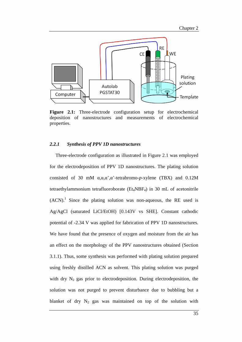
Figure 2.1: Three-electrode configuration setup for electrochemical deposition of nanostructures and measurements of electrochemical properties.
2.2.1 Synthesis of PPV 1D nanostructures
Three-electrode configuration as illustrated in Figure 2.1 was employed
for the electrodeposition of PPV 1D nanostructures. The plating solution
consisted of 30 mM α,α,α’,α’-tetrabromo-p-xylene (TBX) and 0.12M
tetraethylammonium tetrafluoroborate (Et4NBF4) in 30 mL of acetonitrile
(ACN).1 Since the plating solution was non-aqueous, the RE used is
Ag/AgCl (saturated LiCl/EtOH) [0.143V vs SHE]. Constant cathodic
potential of -2.34 V was applied for fabrication of PPV 1D nanostructures.
We have found that the presence of oxygen and moisture from the air has
an effect on the morphology of the PPV nanostructures obtained (Section
3.1.1). Thus, some synthesis was performed with plating solution prepared
using freshly distilled ACN as solvent. This plating solution was purged
with dry N2 gas prior to electrodeposition. During electrodeposition, the
solution was not purged to prevent disturbance due to bubbling but a
blanket of dry N2 gas was maintained on top of the solution with

Chapter 2
36
continuous flow of N2 gas. In order to study the effect of applied potential
on the morphology of PPV nanostructures in Section 3.1.2, constant
potentials ranging from -1.74 V to -2.74 V was chosen to electropolymerize
PPV into the pores of AAO template. After electrodeposition, the template
was removed by soaking in 0.5 M NaOH solution for 1 hour to give free-
standing array of 1D nanostructures on the thin gold substrate. A schematic
diagram of the template-assisted synthesis of PPV nanowires (NWs) or
nanotubes (NTs) is illustrated in Figure 2.2.
Figure 2.2: Schematic diagram for the synthesis of PPV 1D nanostructures by electrodeposition using AAO as template.
2.2.2 Electrodeposition of polypyrrole and metallic components for
core-shell 1D nanostructures
Three-electrode configuration as illustrated in Figure 2.1 was employed
for the electrodeposition of multi-layered core-shell 1D nanostructures in
Chapter 4. Depending on the material of interest to be deposited, the plating
solution and deposition parameters used would be changed accordingly.
For electrodeposition of polypyrrole (PPy), plating solution used
consists of 0.3 M pyrrole and 0.12 M Et4NBF4 with 30 mL ACN as the

Chapter 2
37
solvent. Electrodeposition was carried out at constant potential +1.064V vs
Ag/AgCl (saturated LiCl/EtOH), with charges passed through of 1.0 C.
For nickel (Ni) component, electrodeposition was carried out under a
constant cathodic current density of -5 mA/cm2 from a typical Watts bath
consisting of 165 g/L NiSO4∙6H2O, 22.5 g/L NiCl2∙6H2O and 37 g/L
H3BO3, adjusted to pH 3-4 with H2SO4.2
Lastly, electrodeposition of copper (Cu) was achieved at a constant
cathodic current density of -2 mA/cm2 from a copper complex aqueous
solution consisting of 80 g/L CuSO4∙5H2O, 120 g/L ethylenediamine and
20 g/L KNaC4H4O6∙4H2O.
2.2.3 Synthesis of Co/Al layered double hydroxides hierarchical 1D
nanostructures
Three-electrode configuration as illustrated in Figure 2.1 was also
employed for the fabrication of hierarchical nanostructures of Co/Al
layered double hydroxides (Co/Al-LDH) nanoflakes (NFs) supported on Co
NWs. Firstly, Co NWs were deposited into the nanochannels of AAO
template at a constant cathodic current of -1.5 mA from 30 mL aqueous
solution consisted of 266 g/L CoSO4·7H2O and 40 g/L H3BO3. Since the
plating solution was aqueous, the RE used is Ag/AgCl (3M KCl).
Subsequently, the Co NWs in AAO was rinsed with deionized water and
immersed into 30 mL of 2.5 M NaOH for 1, 18, 24 and 48 hours. These
durations of immersion were chosen to study the effect of alkaline
treatment time in Section 5.1. The alkaline treatment would remove AAO

Chapter 2
38
and form Co/Al-LDH NFs at the same time. This procedure was adapted
from Lee et al. which reported the fabrication of CoOOH NFs on Co foil
using alkaline treatment in a stirred solution.3, 4 A schematic of the
synthesis process is illustrated in Figure 2.3.
Figure 2.3: Schematic diagram for the fabrication of Co/Al-LDH hierarchical nanostructures using AAO as template and source of Al3+ ions.
2.3 Synthesis of 1D nanostructures using aligned MWCNT as
template
In this study, aligned multi-walled carbon nanotubes (MWCNT) was
used as a supporting template for deposition. Here, array of aligned
MWCNT was first prepared on a silicon (Si) substrate, followed by
electropolymerization of PPV onto the MWCNT. The synthesis strategy is
shown in Figure 2.4.

Chapter 2
39
Figure 2.4: Schematic diagram for the growth of MWCNT/PPV core-shell nanostuctures on n-type Si via PECVD followed by electrochemical method.
2.3.1 Synthesis of aligned MWCNT arrays
The arrays of aligned MWCNT was grown using plasma-enhanced
chemical vapour deposition (PECVD) technique5 with iron (Fe)
nanoparticles as catalyst on 1.3 × 1.3 cm n-type Si (100) (doping thickness
500 ± 25 µm, resistivity 1-30 Ω-cm). Before use, the substrates were
cleaned by ultrasonic bath in acetone for 15 minutes, followed by deionised
water for another 5 minutes to remove organic residues and acetone,
respectively. The substrates were then blown dry with nitrogen gas. Then,
the cleaned substrates were subjected to radio frequency (RF) magnetron
sputtering machine to coat a thin layer of Fe catalyst (about 5 nm thickness)
as shown in Figure 2.4 Step 1. Sputtering was carried out at 100 W under
argon gas flow of 20 sccm and process pressure of 12 mTorr for 1 minute

Chapter 2
40
after reaching a vacuum of 2.6 × 10⁻⁶ Torr. Rotation of stage was set to be
at about 12 rpm.
Subsequently, the substrates were transferred into an RF (13.56MHz)
PECVD system where the MWCNT was grown. Once the chamber has
reached vacuum level about 1 × 10⁻⁵ Torr, the temperature for the chamber
and substrates were set at 400 oC and 720 oC, respectively. Next, the
chamber was conditioned with H2 gas (55 sccm) at pressure of 500 mTorr
for 4 minutes. The growth of MWCNT then proceed via two processes: (1)
The Fe layer on Si was etched and reduced by H2 plasma (55 sccm, RF
power 80 W) at substrate temperature of 720 oC and process pressure of
500 mTorr for 10 minutes to form islands of elemental Fe catalyst as shown
in Figure 2.4 Step 2. (2) A mixture of C2H2 (22 sccm) and H2 (55 sccm)
gases was introduced into the chamber at substrate temperature of 720 oC,
working pressure of 1200 mTorr and RF power of 100 W for growth of
MWCNT as shown in Figure 2.4 Step 3. The growth duration was set to 1
hour. Finally, the system was cooled down to room temperature and vented
to atmospheric pressure before the samples were removed.
2.3.2 Synthesis of aligned MWCNT/PPV core-shell nanowires
Using the arrays of aligned MWCNT as-prepared in Section 2.3.1,
MWCNT/PPV core-shell NWs were prepared by coating PPV onto the
MWCNT via electrochemical method as shown in Figure 2.4 Step 4. The
synthesis setup and conditions were similar to that for the synthesis of PPV
nanostructures in Section 2.2.1. Electrodeposition of PPV was carried out

Chapter 2
41
via the three-electrode configuration as shown in Figure 2.1 with the
MWCNT array on Si substrate as WE. A copper tape was used to connect
the conductive surface of the n-type Si to the copper foil in the Teflon cell
to ensure good electrical connection to the MWCNT array, as the bottom
side of the substrate was not conductive. The same plating solution as that
in Section 2.2.1 was employed (30 mM TBX and 0.12 M Et4NBF4) with
the ACN solvent distilled prior to use and the plating solution purged with
nitrogen (N2) before electrodeposition. A blanket of N2 gas was maintained
on top of the solution during electrodeposition to provide a dry and oxygen-
free environment, preventing interferences from the reduction of H2O and
O2 during the synthesis. Optimum parameters for the electrodeposition of
PPV are further discussed in Chapter 6.
2.4 Micro-patterning of PPV 1D nanostructures array via laser
pruning technique
The well-formed PPV nanostructures arrays were subjected to micro-
patterning using laser pruning technique. Details of this technique have
been reported elsewhere.6 In brief, a parallel beam of laser was directed
into a conventional optical microscope whereby it was focused to a tight
spot by the objective lens of the optical microscope system. With the
sample sitting on computer controlled stage, a wide variety of micro
patterns could be readily created. A schematic of the optical microscope-
focused laser beam system set-up is shown in Figure 2.5. The lasers
employed were diode lasers of wavelength 660 nm and 532 nm, with their

Chapter 2
42
laser powers adjusted using a neutral density filter. The raster speed of
patterning was set to be at 65 µm/s.
Figure 2.5: Schematic of the optical microscope-focused laser beam system used for micro-patterning. For laser pruning in air, samples were placed directly under the laser beam as shown in the bottom left box; while the box in the bottom right shows the chamber for laser pruning in vacuum or helium environment.
2.5 Oxygen reactive ion etching (O2 RIE) and heat treatment of
core-shell nanostructures
Oxygen reactive ion etching (O2 RIE) of PPy/Ni core-shell NWs in
Section 4.1.1 was carried out using SAMCO RIE-10N, operated at power

Chapter 2
43
of 20 W and pressure of 0.05 Torr. Samples were placed facing up in the
chamber and etched for 15 minutes.
For the heat treatment of PPy/Ni core-shell NWs to obtain nickel oxide
NTs in Section 4.1.1, samples were placed in the middle of a tube furnace
and treatment was carried out at 400°C in ambient air for 3 hours.
2.6 Measurement of electrochemical capacitance of Co/Al layered
double hydroxides hierarchical 1D nanostructures
An electrochemical half cell was assembled in a three-electrode
configuration as shown in Figure 2.1 with Pt wire as the CE, Ag/AgCl (3M
KCl) as the RE and the Co/Al-LDH nanostructures prepared in Section
2.2.3 as WE. Since the nanostructures are free-standing on gold substrate,
binder was not required to fabricate this WE. The electrochemical
behaviour was studied via cyclic voltammetry (CV) and galvanostatic
charge-discharge (C-D) measurements in 30 mL of 1 M KOH aqueous
solution at ambient condition using Autolab PGSTAT30
potentiostat/galvanostat. CV curves were obtained by scanning the potential
between -0.1 V and 0.5 V at scan rate of 10 mV/s. On the other hand, C-D
curves were recorded at 2.5 mA/cm2, 5.1 mA/cm2 , 10.2 mA/cm2 and 12.7
mA/cm2 in potential range of 0 V to 0.45 V.

Chapter 2
44
2.7 Measurement of electrochemical glucose sensing of Co/Al
layered double hydroxides hierarchical 1D nanostructures
The same three-electrode configuration as described in Section 2.6 and
Autolab PGSTAT30 potentiostat/galvanostat were employed.
To evaluate the glucose (Glc) sensing properties of the Co/Al-LDH
electrodes, CV and hydrodynamic chronoamperometric Glc step addition
were carried out at ambient condition. CV curves in Figure 5.9A were
recorded in potential range of -0.1 V to 0.5 V at 10 mV/s before and after
addition of Glc. Amounts of Glc added were 100 µL, 200 µL and 500 µL of
0.135 M stock solution for corresponding concentrations of 0.5 mM, 1.0
mM and 2.5 mM in 27 mL of 0.1 M NaOH. On the other hand,
hydrodynamic chronoamperometric Glc step addition in Figure 5.10 was
carried out at constant potentials of 0.3 V and 0.4 V with constant stirring
of 700 rpm. Glc was added step-wise at interval of 50 seconds in the
sequence of 10 µL, 20 µL, 40 µL, 80 µL and 100 µL of 0.135 M stock
solution into 27 mL of 0.1 M NaOH for respective added concentration of
0.05 mM, 0.1 mM. 0.2 mM, 0.4 mM and 0.5 mM.
Effect of concentration of NaOH (also pH of the electrolyte) on Glc
sensing was studied in electrolyte concentrations of 0.005 M, 0.01 M, 0.02
M, 0.05 M and 0.1 M NaOH. For each electrolyte, pH of the solution and
the current response at 0.3 V to addition of 4 mM Glc were recorded.
Selectivity of our electrodes were tested against naturally occurring
interfering compounds such as uric acid (UA) and ascorbic acid (AA). The
tests were carried out at 0.3 V to measure current response of 4 mM Glc in

Chapter 2
45
the presence of 0.33 mM of UA and 0.125 mM of AA in 0.1 M NaOH
electrolyte.
2.8 Measurement of photocurrent response of aligned
MWCNT/PPV core-shell nanowires
Here, the MWCNT/PPV core-shell NWs prepared from Section 2.3.2
are tested for their photocurrent (PC) response. Since the n-type Si
substrate may give positive results for current-voltage (I-V) and PC
measurements, the nanostructures were first transferred to a non-conductive
substrate as illustrated in Figure 2.6.
Figure 2.6: Schematic diagram for the measurement of I-V and PC response of MWCNT and MWCNT/PPV core-shell NWs.

Chapter 2
46
Firstly, arrays to be studied were transferred onto double-sided tape
adhered on glass substrate by pressing the array onto the tape, with the
array facing down (Step 1 Figure 2.6). Then, Si substrate was slowly peeled
off, leaving behind the array on the tape (Step 2 Figure 2.6). Both ends of
the sample were subsequently connected to fine copper (Cu) wires using
conductive silver (Ag) paste (Step 3 Figure 2.6). Once the paste dried, the
sample was covered with an opaque card with a small opening of 2 mm × 2
mm, exposing only the middle part of the array to laser irradiation (Step 4
Figure 2.6). During measurements, it was ensured that the electrical
connections at both ends of array were covered to prevent interference due
to irradiation onto the Ag paste electrodes.
The set-up was then connected to Keithley 6430 Source Meter using
metal clips for I-V and PC measurements (Step 5 and 6 Figure 2.6). For I-V
measurement, the voltage was swept from -0.1 V to +0.1 V. For PC
measurement, the current response was recorded over time in the absence
and presence of irradiation at a constant bias voltage of 0.1 V. The presence
of irradiation is denoted as the “on” state and when the beam is blocked, it
is denoted as the “off” state. Blue laser (405 nm) with power of 1.5
mW/mm2 was used as the light source.
2.9 Characterization techniques
2.9.1 Scanning Electron Microscopy (SEM)
SEM was performed in a JEOL JSM 6700-F operating at 10 μA and 5.0
kV to characterize the morphology and dimensions of the nanostructures

Chapter 2
47
obtained. Samples for analysis were prepared by sticking the free-standing
array of nanostructures (which remained on their respective substrates) onto
a metal stud (sample holder). The samples were then mounted into the SEM
chamber for analysis. Samples with less conductive surfaces were sputtered
with a thin layer of platinum using JEOL JFC-1600 Auto Fine Coater
(operating at -20mA for 45s) before analysis.
2.9.2 Transmission Electron Microscope (TEM) and High Resolution
TEM (HRTEM)
TEM was performed in a JEOL JEM 2010F with an acceleration voltage
of 200 kV whereas HRTEM in a JEOL JEM 3010 with an acceleration
voltage of 300kV. Sample preparation for TEM characterization varies for
different type of nanostructures prepared in this thesis. For PPV samples in
Chapter 3, the gold substrate was firstly removed by dipping into
HNO3:HCl = 1:3 mixture solution. The samples were rinsed with deionized
water before releasing the nanostructures from AAO template using 0.5 M
NaOH. The products were washed and centrifuged using distilled water
until pH 7 was reached, followed by dispersion in ethanol. In Chapter 6,
samples of MWCNT and MWCNT/PPV were prepared by scrapping off
small bits of the nanostructures from the Si substrate and dispersed into
100µL of ethanol in microcentrifuge tube. Each solution containing the
dispersed nanostructures was dripped onto a 200 mesh carbon-coated
copper grid and dried in vacuum before TEM analysis.

Chapter 2
48
2.9.3 Energy Dispersive X-ray Spectroscopy (EDX)
EDX analysis was carried out in a JEOL JSM 6701-F electron
microscope operating at 10 μA and 15.0 kV, equipped with EDX detector.
Samples for analysis were prepared by sticking the free-standing array of
nanostructures (which remained on their respective substrates) onto a metal
stud (sample holder). The samples were then mounted into the SEM
chamber for analysis.
2.9.4 Diffuse Reflectance Fourier-Transform Infrared (DR-FTIR)
DR-FTIR spectra were obtained from Nicolet Continuµm FT-IR
Microscope using reflectance mode. Samples to be analyzed would need to
be on gold substrate for better signals. Since the PPV samples in Chapter 3
were free-standing on gold substrate, there was no need for further sample
preparation.
2.9.5 Raman Scattering Spectroscopy
Micro-Raman spectra were obtained from Renishaw inVia Raman
Microscope. For PPV samples in Chapter 3, laser excitation at 785 nm was
chosen to avoid high fluorescence background interference which was
observed if 532 nm was to be used as excitation source. As for Chapter 6,
excitation wavelengths at 532 nm, 633 nm and 785 nm were employed and
the differences in the Raman spectra are discussed in the Chapter. All
Raman analyses were carried out directly on the free-standing
nanostructures on substrate.

Chapter 2
49
2.9.6 UV-Visible Absorption Spectroscopy
UV-visible absorption spectra were acquired from Shimadzu UV-3600,
attached with integrated sphere. For the as-grown PPV samples in Chapter
3, the measurements were carried out with the nanostructures still
embedded in AAO with the gold substrate removed. A baseline was
obtained using pristine AAO membrane before measurement. As for the
MWCNT and MWCNT/PPV core-shell NWs in Chapter 6, samples were
prepared by scrapping the nanostructures from the Si substrate and blended
with BaSO4 using mortar and pestle. The mixture was then pressed onto
sample holder. A baseline was obtained using BaSO4 before measurements.
2.9.7 Photoluminescence (PL) Spectroscopy
In Chapter 3 and Chapter 6, selective-area PL spectra of the PPV NWs
and NTs arrays (before and after laser patterning) and MWCNT/PPV
nanostructures were obtained from Renishaw inVia Raman Microscope
with laser excitation at 325 nm at room temperature. Analyses were carried
out directly on the free-standing nanostructures without need of additional
sample preparation.
2.9.8 Fluorescence Microscopy (FM)
In Chapter 3, the fluorescence images of the patterned PPV arrays were
obtained from Nikon Eclipse Ti Inverted Microscope. Illumination source
was Mercury arc lamp and the filter used was UV-1A (excitation filter at

Chapter 2
50
360-370 nm, dichromatic mirror cut-on at 380 nm, barrier filter cut-on at
420 nm).
2.9.9 X-ray Diffraction (XRD)
XRD patterns were recorded using a Philips X-ray diffractometer with
Cu Kα radiation (λ = 1.54187 Å) scanning in the 2θ range of 10°-80°. The
free-standing arrays of nanostructures were placed onto a glass slide and
then mounted on the sample holder in the instrument for measurement.
2.9.10 X-ray Photoelectron Spectroscopy (XPS)
In Chapter 3, XPS measurements were performed on Kratos Analytical
Axis Ultra DLD using monochromated Al Kα (1486.6 eV) X-ray source at
emission current of 10 mA and voltage of 15 kV. To characterize the
surface of PPV nanostructures before and after laser treatment, the scan
spot size was fixed approximately at 220 µm, which is smaller than the
region of 600 × 600 µm treated with laser.
2.10 References
1. T. H. Kim, S. M. Park. Electrochim. Acta 50 (2005) 1461-1467.
2. G. A. DiBari. Plat. Surf. Finish. 91 (2004) 23-26.
3. K. K. Lee, P. Y. Loh, C. H. Sow, W. S. Chin. Electrochem.
Commun. 20 (2012) 128-132.
4. K. K. Lee, P. Y. Loh, C. H. Sow, W. S. Chin. Biosens. Bioelectron.
39 (2013) 255-260.

Chapter 2
51
5. Y. H. Wang, J. Lin, C. H. Huan, G. S. Chen. Appl. Phys. Lett. 79
(2001) 680-682.
6. K. Y. Lim, C. H. Sow, J. Y. Lin, F. C. Cheong, Z. X. Shen, J. T. L.
Thong, K. C. Chin, A. T. S. Wee. Adv. Mater. 15 (2003) 300-303.

Chapter 2
52
53
Chapter 3
Fabrication and Micro-Patterning of Luminescent
Poly(p-phenylene vinylene) Nanowire and Nanotube
Arrays
Conducting polymers (CPs) have attracted much attention due to their
chemically tuneable optical and electronic properties, as well as their ability
for solution processing.1, 2 These polymers have extended π-conjugation
typically arises from alternating single and double C-C bonds along their
polymer backbone. Some examples of conducting polymers are
polyacetylene (PA), polypyrrole (PPy), polythiophene (PTh), polyaniline
(PANI) and poly(p-phenylene vinylene) (PPV). 1D nanostructures
fabricated from such polymers have been the subject of recent active
research to exploit their unique physical, chemical, electronic and photonic
properties.3-6 One important aspect in the CPs NWs technologies is to
develop reliable methods for the production of such nanostructures with a
good control over critical parameters such as diameter, length, morphology,
and chemical composition.
PPV consists of alternating benzene ring and C=C double bonds along
its polymer chain. It is well-known to exhibit photoluminescence (PL),7
electroluminescence,8 and non-linear optical properties.9 Despite all these
potentials, fabrication of PPV in an intended shape of a desired dimension
is extremely challenging due to the insolubility of PPV in any solvent and

Chapter 3
54
to its intractability. Therefore, one has to rely on soluble precursors that can
be converted chemically or thermally to the final composition. The
sulphonium precursor route first described by Wessling and Zimmerman10
is one of the most widely used method.8, 11, 12
Hence, in the literature PPV NWs or NTs have been prepared from
soluble precursor polymers into the desired morphology followed by
thermal conversion. Some examples are chemical vapour deposition (CVD)
polymerization into AAO template,13 impregnation of precursor solution
into AAO template14 and electrospinning.15-17 In general, these methods are
tedious and/or costly as they require long hours of preparation and
purification of the precursor, post-treatment of samples to convert the
precursors to PPV, high temperature furnace and vacuum system. In
addition, side products have to be removed during these processes, which
are expected to generate many defects such as impurities and bubbles in the
final product.
In this chapter, arrays of PPV 1D nanostructures were prepared by a
simple electrochemical reduction of α,α,α’,α’-tetrabromo-p-xylene (TBX)
into the nanochannels of AAO. While electrodeposition of PPV films had
been reported,18, 19 our work adapted the electrodeposition parameters
together with AAO template to directly prepare free-standing arrays of PPV
1D nanostructures. We established optimal parameters for the
electrodeposition into the AAO nanochannels and found that the
morphology and length of the nanostructures were affected by the purity of
plating solution, applied cathodic potential and amount of charge deposited.

Chapter 3
55
In Section 3.2, we further demonstrated the ability to micro-pattern the PPV
arrays using focused laser beam. A “red-shift” of the PL peak of PPV upon
laser modification in ambient was observed. Further studies were carried
out in attempt to understand the phenomenon.
3.1 PPV 1D nanostructures
Electrodeposition of PPV nanostructures was detailed in Section 2.2.1.
Constant-potential coulometry was carried out to prepare PPV
nanostructures inside the pores of AAO membrane. The template was then
removed, giving free-standing array of PPV nanostructures on the gold
substrate. The mechanism for electrochemical synthesis of PPV from TBX
proposed by Kim et al.18 is as shown in Figure 3.1.
Figure 3.1: The mechanism for electrochemical polymerization of PPV from TBX as proposed by Kim et al.18

Chapter 3
56
3.1.1 Effects of oxygen and moisture in the plating solution
Electropolymerization of PPV from the acetonitrile (ACN) (as-received)
plating solution at constant potential of -2.34 V resulted in well-formed
free-standing PPV NWs arrays as shown in Figure 3.2. As expected, the
length of PPV NWs increased with an increase in charge deposited (Figure
3.2A-C). The correlation is illustrated by a plot of length versus charge
deposited in Figure 3.2E. A self-limiting plateau was obtained, indicating
that PPV NWs can be grown controllably up to about 1.2 µm in length with
this method.
It was observed, however, that the tips of the NWs were not as well-
formed when deposited with cathodic charge of 2.0 C and above (Figure
3.2D). This is probably due to bubbles that were observed on the surface of
the AAO template during prolonged electrodeposition time. These bubbles
were most likely hydrogen gas created from the reduction of oxygen and
moisture in the plating solution. The reaction equations and their respective
standard electrode potentials are summarized as follow:
O2 (g) + 2H2O (l) + 4e- 4OH- (aq) E0 = 0.4 V (vs SHE) … (3.1)
O2 (g) + 4H+ + 4e- 2H2O (l) E0 = 1.23 V (vs SHE) … (3.2)
2H2O (l) + 2e- H2 (g) + 2OH- (aq) E0 = -0.83 V (vs SHE) … (3.3)

Chapter 3
57
Figure 3.2: SEM images of PPV NWs electrodeposited at -2.34 V for cathodic charge of (A) 0.26 C, (B) 0.5 C, (C) 1.0 C and (D) 2.0 C. Insets show the side-view of the NWs. (E) A plot of the length of PPV NWs synthesized as a function of charge deposited. The line is drawn as a guide.

Chapter 3
58
Since the deposition of larger amount of charge would necessitate longer
deposition time, constant agitation from the bubbles formed would have
affected further growth of PPV at the tips of the NWs during prolonged
deposition. These tips could collapse after the removal of AAO template,
forming ruptures or particles on top of the array. As observed in Figure
3.2D, this left behind short segments of NWs standing on the gold substrate.
On the other hand, we observed that different nanostructure morphology
was obtained when the ACN solvent was distilled prior to use and the
plating solution was purged with N2 gas. For the convenience of our
discussion, we refer this synthesis procedure as using “distilled ACN"
solution. With the removal of moisture and oxygen from the plating
solution through distillation and purging, well-formed arrays of PPV NTs
were obtained using the same set-up and synthesis parameters (Figure
3.3A-D). These NTs were well-formed even when deposited at extended
duration at cathodic charge of 2.0 C. However, the tubular section of the
nanostructure was only found near the tips of NTs as clearly illustrated in
the TEM images in Figure 3.3C-D. This NT-NW hybrid structure is quite
common for conducting polymers grown by electrochemistry method using
AAO as template.20-22 The plot of length of NTs versus the amount of
charge deposited in Figure 3.3E suggested a better linear correlation than
that in Figure 3.2E. Thus, PPV NTs with much longer length can be
prepared at the same amount of charge using distilled ACN plating solution.

Chapter 3
59
Figure 3.3: SEM images of PPV NTs electrodeposited at -2.34 V using distilled ACN plating solution for cathodic charge of (A) 0.26 C and (B) 2.0 C. The insets show side-view of the NTs. TEM images of PPV NTs prepared for cathodic charge of (C) 0.26 C and (D) 1.0 C. (E) A plot of the length of PPV NTs synthesized as a function of charge deposited.

Chapter 3
60
The well-deposited PPV NTs from distilled ACN confirmed that the
presence of moisture and oxygen have much effect on the electrodeposition
of PPV in the AAO templates. We hypothesized that, in the presence of
moisture and oxygen in the solution, bubbles evolved from the gold WE
would disturb and increase the diffusion of monomers into the
nanochannels. At constant deposition rate (i.e. applied potential), such
increase in diffusion will lead to sufficient supply of monomers into the
nanochannels and the formation of NWs. On the contrary, when both
oxygen and moisture were removed, there were no bubbles evolved and
diffusion would be slower, resulting to the growth of NTs at the same
deposition rate. In addition, side reactions as indicated by Equations (3.1)
to (3.3) would also affect the actual amount of charge contributing to the
growth of PPV, i.e. shorter NWs were obtained at the same amount of
charge deposited as the NTs.
3.1.2 Effects of applied potential
Next, we investigated the effect of applied potential used in
electrodeposition. For electrodeposition in as-received ACN plating
solution, NWs were obtained at cathodic potentials of -2.04 V and -2.34 V
as shown by TEM images in Figure 3.4A and Figure 3.4B, respectively.
When the cathodic potential was increased to -2.74 V, tubular section was
observed at the tip of the nanostructure but was not well-formed (Figure
3.4C). On the other hand, electrodeposition in distilled ACN plating
solution gave tubular NTs at -2.34 V (Figure 3.3 and Figure 3.4E), and the

Chapter 3
61
tubular section was found to decrease as the applied cathodic potential
decreases from -2.04 V to -1.74 V (Figure 3.4D). These observations are
similar to those reported for electrodeposition of CPs where an increase in
deposition potential often gave more tubular nanostructures, which was
explained by the diffusion mechanism.20-23 Thus, at higher deposition
potentials and the same precursor concentration, deposition rate is
increased but growth is limited by diffusion of monomers, leading to the
formation of NTs. Besides, it was also proposed that polymer tends to
nucleate and grow from the channel walls of AAO due to attractive
interaction such as solvophobic and electrostatic interactions between the
reacting species and pore walls.24, 25
Other than morphology change, the nanostructures appeared to be longer
for increasing cathodic potentials in both plating solutions. As the rate of
electrodeposition increases with cathodic potential, the same amount
deposited may have spread out to form tubular structures thus resulting in
longer nanostructures.
To illustrate the correlation of tubular length and applied potential, a
graph of relative tubular length against the applied cathodic potential was
plotted in Figure 3.4F. This plot excluded the samples prepared at -2.74 V
in the as-received ACN solution as they were not well-formed. There is no
clear correlation obtained from these plots; nevertheless, it is evident that
synthesis in distilled ACN always produces relatively longer tubular
segment compared to that in the as-received ACN at the same amount of
cathodic charge.

Chapter 3
62
Figure 3.4: TEM images of PPV nanostructures electrodeposited from (A-C) as-received and (D-E) distilled ACN plating solutions for cathodic charge of 1.0 C at the potentials specified. (F) Plot of tubular portion versus applied cathodic potential.

Chapter 3
63
In the following discussion, we have chosen to prepare PPV
nanostructures at an optimal cathodic potential of -2.34 V for cathodic
charge of 0.26 C. For convenience, we will label the samples obtained from
the as-received ACN solution as PPV NWs while those from distilled ACN
solution as PPV NTs.
3.1.3 Characterization of PPV nanostructures
The PPV nanostructures were characterized using DR-FTIR (Section
2.8.4) and micro-Raman (Section 2.8.5) to validate the successful
electropolymerization of PPV. Typical IR and Raman spectra obtained are
shown in Figure 3.5A and Figure 3.5B, respectively. Overall, the peak
assignments (as tabulated in Table 3.1) are in good agreement with those
reported for chemically-synthesized PPV films.26 However, these PPV
NWs and NTs may have some extent of oxidation along the polymer chain
as shown by the presence of 1695 cm-1 peak in the IR spectra (Figure 3.5A),
which could be assigned to the carbonyl C=O stretching mode. Thus,
oxidation may have occurred during the synthesis. In the Raman spectra in
Figure 3.5B, the presence of a weak 963 cm-1 band may reflect slight
distortion of vinylene group from its planar trans form.27 From studies of a
series of oligophenylene vinylenes (OPVs),28-31 it was reported that the
relative ratio of peak intensities of 1552 cm-1 (mainly ring stretching) to
1628 cm-1 (mainly vinyl C=C stretch) increases with increasing number of
repeating monomer units, and is up to 1 for the polymeric PPV. In our case,

Chapter 3
64
the relative ratios obtained were found to be about 0.49 and 0.50
respectively for PPV NWs and NTs, suggesting shorter conjugation lengths.
Figure 3.5: Representative (A) DR-FTIR and (B) Raman spectra of PPV NWs and NTs, with the characteristic FTIR and Raman peaks of PPV as labelled.26 Detailed assignment is given in Table 3.1. Raman spectra were displaced for ease of comparison.

Chapter 3
65
Table 3.1: Assignments of the observed vibrational bands of PPV.26
FTIR Raman ν (cm-1) Mode ν (cm-1) Mode
835 C-H out-of-plane bend
for p-disubstituted benzene ring
963 C-H out-of-plane bend
966 C-H out-of-plane bend of trans-vinylene 1173 C-H in-plane bend
1018 CH in-plane bend 1322 Vinyl CH in-plane bend
1109 CH in-plane bend 1414 Ring stretch & in-plane deformation
1213 Vinyl CH in-plane bend 1552 Ring stretch
1275 Ring stretch 1592 Ring stretch, Vinyl C=C stretch
1417 Ring stretch and in-plane deformation 1628 Vinyl C=C stretch, ring
stretch
1512 Ring stretch and in-plane deformation
3025 Vinyl CH stretch
Normalized UV-visible absorption and PL spectra of PPV NWs and NTs
are shown in Figure 3.6. Samples preparations for both characterization
methods were detailed in Section 2.8.6 and Section 2.8.7, respectively. For
PPV NWs, it was observed that the absorption edge onset is at 442 nm and
the absorption maximum appears near 337 nm. For PPV NTs, the onset is
at 467 nm and a peak near 345 nm. The NWs exhibited absorption onset
and peak at shorter wavelength than the NTs, although both of these values
are at shorter wavelength compared to those reported.7, 32 Studies of a series
of OPVs had observed red-shift of absorption wavelengths with increasing
number of repeating monomer units.28-31 Various theoretical calculation
methods were also applied and all demonstrated that the π-π* gap decreases

Chapter 3
66
with increase conjugation length. This suggests that the PPV obtained from
our synthesis has relatively shorter conjugated chain lengths, which
matches the observation derived from IR and Raman studies above. The
relatively more blue-shifted absorption for the NWs may also indicate the
formation of shorter conjugation chain length due to faster rate of
electrodeposition as compared to the NTs.
Figure 3.6: UV-visible absorption and PL spectra of PPV NWs and PPV NTs arrays. (Excitation wavelength for PL: 325 nm)
For the PL spectra in Figure 3.6, both the NWs and NTs showed a broad
peak with maximum at 533 nm and 558 nm, respectively, at excitation
wavelength of 325 nm. A stokes shift between the absorption and PL
maxima indicates that there were relaxations of the excited state before

Chapter 3
67
emission. This broad PL profile is similar to that observed for PPV film
prepared via electrochemical method,32 which is rather lack of resolved
vibronic progressions as compared to chemically prepared PPV.7, 14, 16
3.2 Micro-patterning of PPV nanostructures array via laser
pruning technique
3.2.1 Laser pruning of PPV nanostructure arrays
The well-formed PPV nanostructures arrays were then subjected to
micro-patterning using laser pruning technique33 as described in Section 2.4.
As an initial attempt, a diode laser of wavelength 660 nm (red laser) was
employed and laser power was varied from 20 mW to 40 mW. It was found
that the focused laser beam at power at or above 20mW readily cuts away
the directly exposed PPV NWs and NTs. The patterns obtained and the
areas cut with laser power of 40 mW were imaged using SEM as shown in
Figure 3.7. Based on the tilted views at the bottom panels of each figure in
Figure 3.7, the high laser power had trimmed away almost all of the PPV
NWs and NTs arrays in the exposed areas. The high-power laser has
transferred large amount of energy to the nanostructures, which could then
burn/cut away the organic nanostructures that were exposed to the focused
laser beam.

Chapter 3
68
Figure 3.7: SEM images of patterns and areas cut using 40mW focused red laser for (A) PPV NWs array and (B) PPV NTs array. Top panels show top views of the laser-pruned patterns. The alphabets “NUS” are the uncut arrays while the surrounding square areas were cut away. Bottom panels show tilted views of the nanostructures areas after laser pruning.

Chapter 3
69
3.2.2 Optical properties of laser-modified PPV arrays
These regions treated by laser were readily identified under the optical
microscope, hence micro-PL spectra (excitation wavelength = 325 nm)
from these regions could be captured. The PL spectra for areas cut by
various laser powers as well as those of the as-grown PPV NWs and NTs
were compared. It should be noted that the overall PL intensities for areas
modified by laser are much lower than that of the as-grown PPV
nanostructures. This is expected since PL signal arise from the emitting
polymer nanostructures and there is less remained after the laser pruning.
Thus, these PL spectra, as presented in Figure 3.8, were normalized for
better comparison. From here, we observed interestingly that laser pruning
gave rise to an apparent “red-shifting” of the PL maxima, which appears to
be increasing with increasing laser power used. At higher laser power, we
had only expected larger amounts of PPV would be removed. However,
such red-shift is relatively less obvious for the controlled samples cut under
inert atmosphere, i.e. vacuum (2 mTorr) and helium (200 mTorr)
environment (Figure 3.8).

Chapter 3
70
Figure 3.8: PL spectra of (A) PPV NWs and (B) PPV NTs arrays, as-grown and laser-modified (at power 20, 30 and 40 mW) in air, vacuum and helium by focused red laser. (Excitation wavelength: 325 nm)
This apparent “red-shifting” of the PL maximum is also displayed by a
change of emission colour observed under fluorescence microscope
(Section 2.8.8). The representative images are shown in Figure 3.9A and
Figure 3.9B for PPV NWs and NTs, respectively. The greenish blue

Chapter 3
71
regions are the as-grown PPV nanostructures, while the darken regions are
the cut areas. Note that the region modified by 40 mW laser in air appears
now in orange-brownish colour. Areas modified in vacuum and helium
environment are dark, nevertheless, due to diminished emission intensity.
Figure 3.9: Fluorescence microscopic images of patterns cut on (A) PPV NWs array and (B) PPV NTs arrays using 40 mW red laser (660 nm) in air, vacuum and helium environment.
3.2.3 Effect of focused laser beam on PPV NTs arrays
Since the red-shift of PL maxima was more significant in samples
modified in the air, it was suspected that the phenomenon could be related

Chapter 3
72
to the oxidation of PPV. This led us to investigate changes in the chemical
structures of PPV upon laser pruning in air and in inert environment. Given
that the chemical structure is the same for both PPV NW and NT
nanostructures and similar effects have been observed in both vacuum and
helium environment, we will focus the following discussions on NTs
sample and laser pruning only in air and in vacuum.
To characterize changes of functional groups on the PPV, DR-FTIR and
Raman spectra were obtained before and after the modification in air and
vacuum. From the DR-FTIR spectra as shown in Figure 3.10A, it was
observed that peak area at 1275 cm-1 and 1695 cm-1 increased significantly
while the 966 cm-1 peak diminished with increasing laser power for
samples modified in air. These peaks (as indicated by the arrows in the
figure) correspond to the C-O stretching for carboxyl group, C=O
stretching for carbonyl group and C-H out-of-plane bending of trans-
vinylene mode, respectively.34 For samples modified in the vacuum, the
increase of 1695 cm-1 peak seems to be less than that treated in air. These
observations point towards focused laser-induced oxidation of PPV upon
laser pruning, to larger extent in the air.34

Chapter 3
73
Figure 3.10: (A) DR-FTIR and (B) Raman spectra of PPV NTs, as-grown and laser-modified in air and vacuum by focused red laser.
A comparison of Raman spectra shown in Figure 3.10B indicated no
new peaks for samples modified with laser either in air or in vacuum.
Generally, the peak intensities decreased with increasing laser power. But,
as laser power increases, there is also an increase in the background of the
spectra, at a larger extent for samples modified in air. This is especially

Chapter 3
74
obvious for laser pruning in air at 40 mW where the baseline already starts
at a rather high Raman intensity. This may be due to high fluorescence
background interference27 and corresponds to the red-shifting of PL
maximum upon laser pruning in air as shown in Figure 3.8B.
In order to compare the elemental composition of PPV array before and
after laser modification, XPS spectra were obtained for Br 3d, C 1s and O
1s peaks as shown in Figure 3.11. Details of the measurement were shown
in Section 2.8.10. For ease of comparison, the integral intensities are
calibrated to unity and offset for display. As-grown PPV NTs was found to
contain minute amount of Br with a peak at 71.2 eV as shown in Figure
3.11A. The amount of Br is about 2 % of the total content as estimated
from peak area. Referring to the synthesis mechanism in Figure 3.1, Br may
present as end groups in probable termination by dimerization. The
presence of Br may also arise from minor incomplete electropolymerization.
However, upon laser pruning, no Br 3d peak was observed, indicating the
laser beam had removed this impurity from the surface.
For the C 1s and O 1s core levels, their XPS spectra are as shown in
Figure 3.11B and Figure 3.11C. It was noted that the C 1s peaks for
samples modified in vacuum have similar peak profile as that for the
untreated PPV array. For samples modified in air at high laser power,
nevertheless, the C 1s peak broadened and the intensity decreased. O 1s
peak for samples modified in air also broadened but the intensity increased
compared to the as-grown PPV NTs. The increased amount of oxygen

Chapter 3
75
agrees with the increase of C=O stretching IR mode as shown in Figure
3.10A, indicating larger extent of oxidation upon laser modification in air.
Figure 3.11: XPS spectra for (A) Br 3d, (B) C 1s and (C) O 1s binding energy for PPV NTs, as-grown and after laser pruning in air and vacuum using focused red laser. All spectra are normalized with their integral intensities calibrated to unity and offset for ease of comparison.
To evaluate the change in the chemical states, the C 1s and O 1s peaks
for both as-grown and laser-modified (in air at 30mW) PPV samples, were

Chapter 3
76
fitted as shown in Figure 3.12. For the as-grown sample, three components
were fitted for the C 1s spectrum (Figure 3.12A). The maximum
component at 285.2 eV is due to the aromatic carbons in PPV structure,
286.9 eV is for C-O carbon and 288.1 eV is for C=O carbon.35, 36 On the
contrary, the C 1s spectrum of the laser-modified PPV has four components
fitted (Figure 3.12C). The additional peak of ~18.5 % of fitted area appears
at lower binding energy of 283.8 eV, and is commonly assigned to
graphitic C. In addition, the total normalized peak area for oxygen-attached
carbons were increased, from 44.4 to 51.0 upon laser modification in air
(Table 3.2).
In agreement with the DR-FTIR results, O 1s peak is detected for the
untreated sample indicating slight oxidation of the polymer chain after
synthesis. As shown in Figure 3.12B, this peak can be fitted to two
components at 533.5 eV and 532.4 eV. The same two components are
found in the corresponding O 1s spectrum of the laser-modified PPV except
with an overall increase in intensity (Figure 3.12D). Total peak area was
increased from 26.1 to 48.2 (Table 3.2). Thus, we conclude that laser
pruning in air had resulted in the oxidation and graphitization of PPV.

Chapter 3
77
Figure 3.12: XPS spectra for C 1s and O 1s of PPV NTs: (A), (B) as-grown, (C), (D) modified in air using 30 mW focused red laser.
Table 3.2: Peak areas for all fitted components of C 1s and O 1s XPS spectra as shown in Figure 3.12. Data were normalized by respective atomic sensitivity factor (ASF) and number of scans.
Component Normalized peak area
As-grown PPV Laser-modified PPV C (graphite) - 98.4 C (Ar) 418.9 380.4 C (C-O) 31.2 36.6 C (C=O) 13.2 14.4 O (C=O) 21.2 19.7 O (C-O) 4.9 28.5

Chapter 3
78
In order to further study the effect of laser treatment, we computed the
ratios of FTIR peak area at 1695 cm-1 (C=O stretching) to 1512 cm-1 (ring
stretching and in-plane deformation), and also the ratio of XPS O 1s peak
area to C 1s peak. We plotted these ratios as well as the PL peak maximum
as a function of laser power as shown in Figure 3.13. It is apparent that both
the FTIR peak area ratio and the computed XPS elemental ratio increase
steadily with laser power. In both cases, the increase is most obvious for
laser power at 20 mW, and samples cut in air always showed higher ratios
as compared to those cut in vacuum. Comparing with the PL shift, we noted
that there was no obvious red-shift for samples cut at 20 mW in both air
and vacuum, although the general increasing trend is similar at higher laser
power.
The above results from DR-FTIR and XPS confirmed that PPV had
undergone oxidation upon laser pruning in air. Oxidation could be induced
by the high local temperature generated by the focused laser beam,
particularly in the presence of surrounding oxygen. It was known that
oxidation of PPV (either thermally or photo-induced) commonly occur at
the vinylene groups; free radicals are generated and carboxyl functional
groups are formed, resulting in the scissions of polymer chains.37 In studies
that had employed broad band light with wavelengths > 300 nm and
unfocused lasers (456 nm and 514 nm) as global irradiation source, a blue-
shift in the UV-visible absorption peak was observed and attributed to
shortening of polymer chains due to oxidation.34, 37, 38 It was also mentioned
that the PL spectral position remained unchanged due to diffusion of

Chapter 3
79
exciton to non-degraded layer of polymer film. To the best of our
knowledge, there has been no report on red-shifting of PL peak of PPV
upon laser irradiation in air.
Figure 3.13: Effect of laser power used for patterning on the (A) FTIR peak area ratio of 1695 cm-1 to 1512 cm-1, (B) XPS peak area ratio of O 1s to C 1s peaks and (C) PL maxima of PPV NTs, for samples treated in air and in vacuum. Excitation wavelength for PL: 325 nm.
To compare photo-induced oxidation of our PPV NTs to that reported of
PPV films, blue laser (405 nm, unfocused) was globally irradiated on the
PPV NTs array for 26 minutes and the samples were analyzed. Similar to
those reported,34, 37, 38 UV-visible absorption spectra were blue-shifted upon
irradiation in air and in vacuum (Figure 3.14A). DR-FTIR spectra also

Chapter 3
80
confirmed an increase of peak area at 1275 cm-1 and 1695 cm-1 (as
indicated by the arrows in the figure), demonstrating the occurrence of
oxidation (Figure 3.14B). However, contrary to the literatures, Figure
3.14C showed that the PL peak of our PPV nanostructures red-shifted upon
irradiation in air by the blue laser, although it remained the same for that
treated in vacuum. This clearly indicated that the observed red-shifting of
PL peak is caused by reasons more than oxidation.
Figure 3.14: (A) UV-visible absorption spectra, (B) DR-FTIR spectra and (C) PL spectra of PPV NTs array before and after global blue laser (405 nm, unfocused) irradiation in air and vacuum. Excitation wavelength for PL: 325 nm.

Chapter 3
81
We further investigated the effect using focused green laser at 532 nm.
As shown in Figure 3.15A, the PL peak red-shifted by about 21 nm for
PPV modified in air at 10 mW, as compared to the as-grown PPV. For
samples modified in vacuum, the PL peaks remained similar at lower laser
power (5 mW) but the intensity diminished completely after 10 mW. It
seems that laser pruning in the vacuum using green laser at high power
could remove the NTs completely. Similarly, oxidation of PPV was
deduced from the DR-FTIR spectra in Figure 3.15B. The IR peak area at
1275 cm-1 and 1695 cm-1 (as indicated by the arrows in the figure)
increased significantly upon laser modification at 5 mW in air, compared to
that in vacuum.

Chapter 3
82
Figure 3.15: (A) PL and (B) DR-FTIR spectra of PPV NTs, as-grown and laser-modified in air and vacuum by focused green laser. (Excitation wavelength for PL: 325 nm)
Compared to red laser, the green laser had caused obvious PL red-shift
effect at even lower laser power (10 mW). This could be due to the higher
absorbance of PPV NTs array at 532 nm compared to that at 660 nm (refer
Figure 3.6). With higher absorbance, the percentage of energy uptake by

Chapter 3
83
PPV from that particular laser wavelength is higher even at the same laser
power. To demonstrate this, a few calculations were carried out using the
following Equation 3.4 to 3.9:
Absorbance, )(log0
10 IIA −= (3.4)
% Absorption of incident radiation, %100)1(0×−=
III abs (3.5)
%100)101( ×−= −A (3.6)
Time taken for laser beam to remain at one position, R
Ldtν
= (3.7)
Energy provided by laser beam, L
LL A
tPE = (3.8)
Energy absorbed by PPV at particular wavelength, Labsabs EIE ×= (3.9)
where I0 and I are the intensities of radiation before and after absorption by
PPV, dL is the diameter of laser beam (~5 µm), νR is raster speed of
patterning (65 µm/s), PL is the laser power (W) and AL is the area of laser
spot (mm2). Results of the calculations were compiled in Table 3.3. The
table clearly illustrates that energies absorbed by PPV at 2, 5 and 10 mW of
focused green laser are similar to that at 20, 30 and 40 mW of focused red
laser, respectively. This suggests a reason for efficient laser pruning of PPV
NTs arrays at laser power as low as 2 mW using focused green laser while
the same occurred at 20 mW for red laser. Similarly, PL red-shift effect was

Chapter 3
84
significant at 10 mW for focused green laser while it was at 30 mW or 40
mW for focused red laser. As for unfocused blue laser irradiation, the
energy absorbed by PPV was actually similar to that when PPV was
subjected to 40 mW focused red laser and 10 mW focused green laser.
Hence, the effect of this global blue laser irradiation may be similar to that
when under these lasers. However, PPV was not visibly cut using the blue
laser, probably because it was not focused to a tight laser spot.
Table 3.3: Energy provided by laser spot and energy absorbed by PPV NTs at the specified wavelengths.
Red Green Blue
λ (nm) 660 532 405 AL
(mm2) 1.963 × 10⁻⁵ 1.963 × 10⁻⁵ 78.54
t (s) 0.0769 0.0769 1560
A 0.0057 0.0320 0.6976
Iabs (%) 1.31 7.11 79.93
PL (mW) 20 30 40 2 5 10 40 0.118
EL (J/mm2) 78.35 117.52 156.70 7.83 19.59 39.17 156.70 2.34
Eabs (J/mm2) 1.03 1.54 2.05 0.56 1.39 2.78 11.14 1.87

Chapter 3
85
3.3 Summary
In summary, free-standing arrays of 1D PPV NWs and NTs were
successfully prepared via electrochemical polymerization of TBX inside
the nanochannels of AAO template. The tubular segment of these NWs and
NTs can be manipulated by using as-received or distilled plating solution as
well as controlling the applied cathodic potential, while their lengths can be
controlled by the electrodeposition duration. DR-FTIR spectra provided
fingerprint of PPV and suggested slight oxidation of the as-grown PPV
NWs and NTs. Comparing the UV-visible absorption with the literatures,
we believe this synthesis method produces PPV with shorter conjugation
lengths of the polymer chains. Both PPV NWs and NTs exhibit intense but
broad PL spectra.
Patterning of PPV NWs and NTs were successfully demonstrated using
laser pruning technique that employs focused laser beam. Both red (660 nm)
and green (532 nm) lasers showed feasibility to pattern the 1D
nanostructures array. Interesting “red-shifting” of the PL maxima was
observed upon laser modification in air but not in inert (vacuum and helium)
environment. This was found to correlate with the oxidation of PPV upon
exposure to focused laser beam. We then attempted to induce photo-
oxidation of PPV NTs via an unfocused blue laser irradiation. Similar to
that observed in the literature, UV-visible and FTIR spectra respectively
indicated scission of polymer chain and increase of C=O peak due to
oxidation. In contrary, PL peak red-shifted upon irradiation in air although
it remained the same for that treated in vacuum. To the best of our

Chapter 3
86
knowledge, there was no report in the literature on oxidation of PPV that
caused red-shifting of PL. Hence, oxidation upon laser modification should
not be the only reason for the red-shifting PL observed.
We postulate that the laser modification may have introduced some trap
intermediate states in the band gap, leading to a red-shift of PL maximum.
However, more studies should be carried out to further understand this
phenomenon.
3.4 References
1. S. R. Forrest. Nature 428 (2004) 911-918.
2. G. Malliaras, R. Friend. Phys. Today 58 (2005) 53-58.
3. A. N. Aleshin. Adv. Mater. 18 (2006) 17-27.
4. J. Jang, V. Springer. Conducting Polymer Nanomaterials and
Their Applications, in: Emissive Materials: Nanomaterials,
Springer-Verlag Berlin, Berlin, 2006, pp. 189-259.
5. L. Liu, Y. M. Zhao, N. Q. Jia, Q. Zhou, C. J. Zhao, M. M. Yan, Z.
Y. Jiang. Thin Solid Films 503 (2006) 241-245.
6. Y. Z. Long, M. M. Li, C. Z. Gu, M. X. Wan, J. L. Duvail, Z. W.
Liu, Z. Y. Fan. Prog. Polym. Sci. 36 (2011) 1415-1442.
7. R. H. Friend, D. D. C. Bradley, P. D. Townsend. J. Phys. D: Appl.
Phys. 20 (1987) 1367-1384.
8. J. H. Burroughes, D. D. C. Bradley, A. R. Brown, R. N. Marks, K.
Mackay, R. H. Friend, P. L. Burns, A. B. Holmes. Nature 347
(1990) 539-541.

Chapter 3
87
9. J. I. Jin, H. K. Shim. Nonlinear-Optical Properties of Poly(1,4-
Phenylenevinylene) and Its Derivatives, in: G.A. Lindsay, K.D.
Singer (Eds.) Polymers for Second-Order Nonlinear Optics, 1995,
pp. 223-238.
10. R. A. Wessling. J. Polym. Sci., Pol. Sym. (1985) 55-66.
11. J. D. Stenger-Smith, R. W. Lenz, G. Wegner. Polymer 30 (1989)
1048-1053.
12. A. Marletta, D. Goncalves, O. N. Oliveira, R. M. Faria, F. E. G.
Guimaraes. Adv. Mater. 12 (2000) 69-74.
13. K. Kim, J. I. Jin. Nano Lett. 1 (2001) 631-636.
14. F. Massuyeau, J. L. Duvail, H. Athalin, J. M. Lorcy, S. Lefrant, J.
Wery, E. Faulques. Nanotechnology 20 (2009) 155701.
15. Y. Xin, Z. H. Huang, E. Y. Yan, W. Zhang, Q. Zhao. Appl. Phys.
Lett. 89 (2006) 053101.
16. W. Zhang, Z. H. Huang, E. Y. Yan, C. Wang, Y. Xin, Q. Zhao, Y.
B. Tong. Mater. Sci. Eng., A 443 (2007) 292-295.
17. Y. Xin, Z. B. Ling, S. Y. Li, T. T. Lin, G. D. Liu. Mater. Sci. Eng.,
B 177 (2012) 1094-1097.
18. T.-H. Kim, S.-M. Park. Electrochim. Acta 50 (2005) 1461-1467.
19. H. Nishihara, M. Akasaka, M. Tateishi, K. Aramaki. Chem. Lett.
(1992) 2061-2064.
20. S. I. Cho, W. J. Kwon, S. J. Choi, P. Kim, S. A. Park, J. Kim, S. J.
Son, R. Xiao, S. H. Kim, S. B. Lee. Adv. Mater. 17 (2005) 171-
175.

Chapter 3
88
21. S. I. Cho, D. H. Choi, S. H. Kim, S. B. Lee. Chem. Mater. 17
(2005) 4564-4566.
22. R. Xiao, S. Il Cho, R. Liu, S. B. Lee. J. Am. Chem. Soc. 129 (2007)
4483-4489.
23. O. Reynes, S. Demoustier-Champagne. J. Electrochem. Soc. 152
(2005) D130-D135.
24. C. R. Martin. Adv. Mater. 3 (1991) 457-459.
25. C. R. Martin. Chem. Mater. 8 (1996) 1739-1746.
26. K. Honda, Y. Furukawa, H. Nishide. Vib. Spectrosc. 40 (2006)
149-154.
27. A. Sakamoto, Y. Furukawa, M. Tasumi. J. Phys. Chem. 96 (1992)
1490-1494.
28. B. Tian, G. Zerbi, R. Schenk, K. Mullen. J. Chem. Phys. 95 (1991)
3191-3197.
29. B. Tian, G. Zerbi, K. Mullen. J. Chem. Phys. 95 (1991) 3198-3207.
30. T. P. Nguyen, V. H. Tran, P. Destruel, D. Oelkrug. Synth. Met.
101 (1999) 633-634.
31. E. Mulazzi, A. Ripamonti, J. Wery, B. Dulieu, S. Lefrant. Phys.
Rev. B 60 (1999) 16519-16525.
32. W. P. Chang, W. T. Whang, P. W. Lin. Polymer 37 (1996) 1513-
1518.
33. K. Y. Lim, C. H. Sow, J. Y. Lin, F. C. Cheong, Z. X. Shen, J. T. L.
Thong, K. C. Chin, A. T. S. Wee. Adv. Mater. 15 (2003) 300-303.
34. T. Zyung, J. J. Kim. Appl. Phys. Lett. 67 (1995) 3420-3422.

Chapter 3
89
35. C. D. Wagner, W. M. Riggs, L. E. Davis, J. F. Moulder. Handbook
of X-ray Photoelectron Spectroscopy: A Reference Book of
Standard Spectra for Identification and Interpretation of XPS
Data G.E. Muilenberg, Perkin-Elmer Corporation, Physical
Electronics Division, Eden Prairie, Minnesota, U.S.A. (1979).
36. G. G. Andersson, W. J. H. van Gennip, J. W. Niemantsverdriet, H.
H. Brongersma. Chem. Phys. 278 (2002) 159-167.
37. S. Chambon, A. Rivaton, J. L. Gardette, M. Firon. Polym. Degrad.
Stab. 96 (2011) 1149-1158.
38. Y. G. Gobato, A. Marletta, R. M. Faria, F. E. G. Guimaraes, J. M.
de Souza, E. C. Pereira. Appl. Phys. Lett. 81 (2002) 942-944.

Chapter 3
90

91
Chapter 4
Synthesis of Controllable Core-shell Nanostructures via
Pore Widening Method
Core-shell NTs and NWs with coupled core and shell materials have
been of great scientific and technological interests due to their potential
applications in solar cells, sensors and energy storage.1-4 Various core-shell
1D hetero-nanostructures have been explored with varied combinations of
semiconductor, metal, metal oxide and conductive polymer.1-16 Some of
these hetero-nanostructured architecture reported functional advantages
such as protection of the core material from oxidation,5 or formation of
coaxial p-i-n junction.1 Others also demonstrated enhanced performance
due to synergistic effect between the core and the shell components.3, 4
Arising from the above advantages, much effort has been dedicated to
explore simple and versatile synthetic strategies to prepare core-shell 1D
hetero-nanostructures. Various synthetic strategies have been proposed,
including redox reaction,6 atomic layer deposition (ALD),7 electrospinning8
and high-temperature chemical vapour deposition (CVD).1, 5, 9-11 However,
these methods often include the use of bulky equipment, high temperature
and high vacuum system which increases the cost of fabrication. Template-
assisted synthesis using nanoporous membranes such as AAO is certainly a
cheaper alternative. A range of methodologies have been employed
together with AAO, such as sol-gel,12 pyrolysis,13 surface thermal

Chapter 4
92
oxidation,14 core shrinkage15 and pore etching,16 to generate core-shell
structures.
One of the attractive attributes of template-assisted synthesis method is
the potential to control the dimensions of the core and shell components
independently. However, it is normally more difficult to control the
thickness of the shell component. In the “core shrinkage” method,15 while
the length of the gold sheath in the polyaniline (PANI)/Au core-shell
nanostructures could be controlled, the control of shell thickness remains a
challenge. Another work which reports on pore-etching using diluted
NaOH solution also did not show control of the shell thickness.16, 17 Fast
dissolution of AAO may make NaOH unsuitable for precise control of the
pore-etching and thus the consequent shell thickness. Hence, it would be
more meaningful to find a general way that can achieve core-shell
structures composed of different materials.
In this Chapter, a versatile “Pore Widening” method that can lead to
various multi-layered 1D hetero-nanostructures with adjustable shell
thickness is reported. Here, diluted phosphoric acid (H3PO4) was used
instead of NaOH, which offers more control on the size of the annular gap
in the AAO nanochannels and consequently the thickness of the shell. The
versatility of this approach would be demonstrated through the fabrication
of various types of bi- and multi-layered core-shell NWs and NTs.

Chapter 4
93
4.1 Synthesis and characterizations of core-shell nanostructures
The strategy for the growth of core-shell nanostructures arrays is
illustrated in Figure 4.1. For demonstration purpose, materials employed
are polypyrrole (PPy) as the conductive polymer and copper (Cu), nickel
(Ni) and gold (Au) as the choice of metal components. Synthesis
parameters for each component were detailed in Section 2.2.2. As shown in
Figure 4.1, polymer (or first metal M1) was first electrodeposited into the
nanochannels of AAO (Step 1). We then immersed the AAO containing the
cores into 6 wt.% H3PO4 (Step 2). Such solution was found to slowly
remove the AAO nanochannel walls, leaving an annular gap around the as-
prepared cores (“Pore Widening”). Metal (or second metal M2) was
subsequently electrodeposited into the gap (Step 3) and 1D core-shell
nanostructure array could be achieved after removing the template with 1M
NaOH (Step 4).
Since 6 wt.% H3PO4 and 1 M NaOH are respectively used for pore-
widening and template removal, the choice of materials for the core and
inner shell layer is limited to those inert to the 6 wt.% H3PO4 and 1 M
NaOH. Nonetheless, through judicious selection of materials and sequences
of steps, this “Pore Widening” method remain versatile and various desired
layered 1D nanostructures can be prepared. Using this “Pore Widening”
strategy as shown in Figure 4.1, deposition of a range of coaxial 1D hetero-
nanostructures such as polymer/metal, metal/metal, polymer/metal/metal
and metal oxide/metal core-shell nanostructures, will be demonstrated in
the following sub-sections.

Chapter 4
94
Figure 4.1: Schematic of the “Pore Widening” steps to generate (A) polymer/metal and (B) metal/metal (M1/M2) core-shell nanostructures.

Chapter 4
95
4.1.1 Polymer/metal core-shell nanowires
Polymer/metal core-shell NWs such as PPy/Ni can be obtained via the
procedure illustrated in Figure 4.1A. In this case, there is no limitation to
the choice of core polymer because most polymers are inert to 6 wt.%
H3PO4 but the shell metal must be inert to 1 M NaOH. Before subsequent
deposition of metal shell, the core (PPy NWs) must be ensured to be longer
than the prospective height of the shell to-be grown so as to prevent the
core from being over-grown by the shell. To enable estimation of the length
of PPy NWs, the growth was first calibrated as function of charge deposited.
Shown in Figure 4.2A is the SEM image representative of the PPy NWs.
From the SEM characterization, length of the NWs with respect to charge
deposited was obtained as shown in Figure 4.2B. As expected, the length of
the polymer NWs increases linearly with respect to the charge deposited.
Figure 4.2: (A) SEM image of as-grown PPy NWs array and (B) graph of length of PPy NWs as a function of charge deposited.

Chapter 4
96
The final PPy/Ni core-shell NWs was characterized using SEM and
Figure 4.3 shows the side views (A and B) and top views (C and D) SEM
images of the core-shell NWs after widening the pores for 1 hour (A, C)
and 2 hours (B, D), respectively. The formation of a layer of metal shell
around the core polymer after the “Pore Widening” procedure is clearly
illustrated. The success of this strategy hinges on the fact that 6 wt.%
H3PO4 can gently dissolve and polish the walls of the AAO nanochannels,
which was the reason for this acid to be widely used in the final step of
making AAO membrane.18, 19 A closer examination of the SEM images
shows that the metal sheath grows thicker with the increase of the pore-
widening time. The average shell thickness are estimated to be 25 nm and
55 nm for the pore-widening time of 1 hour (Figure 4.3A, C) and 2 hours
(Figure 4.3B, D), respectively. This is as expected because the annular gap
is created by the slow dissolution of AAO channel walls by the diluted
H3PO4. The longer the AAO is immersed in the acidic solution for pore-
widening, the more AAO is dissolved to give larger annular gap, leading to
thicker shell layer.

Chapter 4
97
Figure 4.3: Side (A and B) and top view (C and D) SEM images of the PPy/Ni core-shell NWs prepared after pore widening for 1 hour (A, C) and 2 hours (B, D), respectively.
In order to clearly show the shell thickness, the nanostructures were
exposed to oxygen reactive ion etching (O2 RIE) (Section 2.5) for 15 mins
which partially remove the extending PPy NWs. With the obstructing PPy
NWs being removed, the SEM images in Figure 4.4A and B now evidently
show the difference in shell thickness corresponding to varying pore-
widening time. By systematically varying the duration of pore-widening, a
calibration plot of shell thickness as function of pore-widening time was
obtained as shown in Figure 4.4C. Shell thickness was found to increase

Chapter 4
98
linearly with pore-widening time, clearly demonstrating the ability of this
method in controlling the shell thickness. In addition, this method also
enables deposition of shells made of various type of metals, only by using
different plating solution during the stage of metal shell deposition (Step 3
in Figure 4.1A). Now, different PPy/metal core-shell NWs in varying shell
thickness, including Ni, Au and Cu can be readily prepared. One example
shown here in Figure 4.4D is the PPy/Cu core-shell NWs array.
Figure 4.4: (A, B) Top view SEM images of the core-shell PPy/Ni NWs prepared at pore-widening time of (A) 1 hour and (B) 2 hours after exposure to oxygen reactive ion etching for 15 minutes. (C) Graph of Ni shell thickness as function of pore-widening time. (D) Side view SEM image of PPy/Cu core-shell NWs array.

Chapter 4
99
Since it is well-known that polymers can be readily removed by suitable
solvent dissolution or heat treatment,8, 20 they may serve as “soft template”
for the fabrication of NTs with controllable wall thickness via our “Pore
Widening” method. This thus opens up another way of making NTs and
even multi-layered NTs (which will be demonstrated in the following
Section 4.1.4), in addition to previously reported NTs synthesis.8, 12, 21, 22
Here, we illustrate a one-step process to obtain nickel oxide NTs using heat
treatment in air (Section 2.5). Figure 4.5A show the SEM image of the
same PPy/Ni sample as in Figure 4.3A after heat treatment at 400°C for 3
hours in ambient air. Indeed the high temperature burnt away the PPy NWs,
leaving behind an array of free-standing NTs.
After the heat treatment, it is noted that the shell surface become
roughened and the thickness increased from about 25 nm to about 60 nm.
Both these observations suggested that the Ni shell have been oxidized into
Ni oxide during the treatment. This is indeed confirmed by EDX analysis
(Section 2.9.3) as shown in Figure 4.5B, which shows a clear oxygen peak
for sample after the heat treatment. The roughening of the surface and
increased thickness of NTs are due to expansion caused by the intercalation
of oxygen into the crystal lattice of Ni metal during the heat treatment.

Chapter 4
100
Figure 4.5: Analysis of PPy/Ni core-shell NWs shown in Figure 4.3A after heat treatment at 400°C in air for 3 hours. (A) Top view SEM image, and (B) a comparison of the EDX spectra before and after the heat treatment.
4.1.2 Metal/metal core-shell nanowires
This pore-widening approach also allows fabrication of metal/metal
core-shell NWs. As already mentioned, the choice of metal for the core is
limited to those inert to the 6 wt.% H3PO4 used for pore-widening step. The
synthesis procedures follow the steps as illustrated in Figure 4.1B for
deposition of M1/M2 core-shell nanostructures. As an example, Cu/Ni
core-shell NWs was prepared using this method where Cu and Ni are the
M1 and M2, respectively. The resulting morphology is as shown in the
SEM image in Figure 4.6. The Ni shell and Cu core are clearly
distinguishable since the surface of Cu portions often appear roughen due
to the formation of a thin layer of oxide when exposed to air. To further
confirm the location of the Ni shell and Cu core, EDX analyses (Section
2.9.3) were carried out at three different locations: the tip (a), the trunk (b)
and the root (c) of the NWs. From the EDX spectra in Figure 4.6a-c, it is

Chapter 4
101
noticed that the relative intensity of Ni to Cu peak gradually decreases from
the tips to the roots of the NWs. This indicates that Ni shells are grown
capped at the tips of Cu NWs.
Figure 4.6: Cu/Ni core-shell NWs array prepared using the “Pore Widening” method. The EDX spectra on the right were taken at three different locations marked as a, b and c on the SEM image on the left.
A question thus arise: why does the morphology of the metal/metal core-
shell NWs (Figure 4.6) differ from that of the polymer/metal core-shell
NWs (Figure 4.3)? Here, an attempt to rationalize the growth mechanism is
shown schematically in Figure 4.7. While doped PPy is a conductive
polymer, its conductivity is inferior in comparison to metal. Thus, atoms of
the shell metal will have higher tendency to deposit directly onto the gold
cathode, causing the shell growth to start from the bottom of the widened

Chapter 4
102
AAO nanochannels (Figure 4.7A). Similar mechanism had been proposed
for the preparation of PANI/Au core-shell nanostructure.15
Figure 4.7: Schematic of the growth mechanism of (A) polymer/metal and (B) metal/metal core-shell NWs in a single nanochannel of AAO template.
On the other hand, for fabrication of metal/metal (M1/M2) core-shell
NWs, the shell deposition can also occur along the length of the conducting
core metal (M1) inside the widened nanochannels as shown in Figure 4.7B.
Due to “point effect”, the deposition of shell metal (M2) will be more
pronounced on the tip rather than at the root of the core metal. The shell
layer would quickly build up at the tips, blocking any diffusion of metal
ions into the bottom gold cathode. This thus prevents the growth of shell at
the cathode or at the root of the core metal, resulting in something like the
“baseball bat” nanostructure as observed in Figure 4.6.
4.1.3 Multi-layered nanowires
In clear contrast to the “core shrinkage” method,15 deposition is certainly
not limited to one single shell component in our method. Additional “Pore

Chapter 4
103
Widening” step can be advantageously applied to create space for
subsequent deposition of second layer of shell to give multi-layered NWs.
The synthesis steps are as shown schematically in Figure 4.8. Here, the
polymer/metal core-shell NWs obtained after Step 3 in Figure 4.1A is
subjected to second pore-widening step which opens up an annular gap
followed by deposition of second shell layer.
Figure 4.8: Schematic of further “Pore Widening” strategy for synthesis of polymer/metal/metal tri-layered core-shell NWs by repeating steps depicted in Figure 4.1.
An example of such multi-layered core-shell nanostructures is
PPy/Cu/Ni tri-layered core-shell NWs, with the PPy as the core, and Cu
and Ni as the first and second shell layer, respectively. The resulting
morphology is as shown in a typical SEM image in Figure 4.9B. As
observed from this SEM image, the outmost shell layer (Ni) appears to be

Chapter 4
104
coating only at the tips of the inner shell layer (Cu), based on the slight
difference in the brightness of the image.
Figure 4.9: SEM image of PPy/Cu/Ni tri-layer core-shell NWs.
To prove the presumption above, elemental profile of this tri-layered
nanostructure was obtained from EDX line analysis (Section 2.9.3) as
shown in Figure 4.10. It is clearly shown here that the tips of the shell
consists mostly of Ni while nearer to the root of the NWs shows larger
amount of Cu, indicating that the inner shell layer is exposed. These
observations proved that the outmost second metal shell (Ni) is deposited
only at the tips but not at the root of the first metal shell layer (Cu). This
correlates to the “point effect” growth mechanism which was discussed in
previous section (Section 4.1.2) for the deposition of metal/metal core-shell
NWs.

Chapter 4
105
Figure 4.10: EDX line analysis of the tri-layered NWs: (A) SEM image of the PPy/Cu/Ni tri-layered core-shell NWs array and (B) the compositional line profiles probed by EDX along the red line in (A), showing well-correlated Ni and Cu signals along the NW axis.

Chapter 4
106
4.1.4 Multi-layered nanotubes
The versatility of this “Pore Widening” method can be further
demonstrated by generating multi-layered NTs via a sensible selection of
materials and sequences of steps. As an example, Figure 4.11 shows the
utilization of the “Pore Widening” method to fabricate metal oxide/metal
double-walled NTs (DWNT). In this case, PPy/Cu core-shell NWs obtained
via procedures in Figure 4.1A would be the starting material. The core-shell
NWs was then subjected to further pore-widening step to provide additional
space for deposition of second layer of shell. Subsequently, the sample was
heated to 300 °C for 40 minutes to decompose the PPy core as well as to
oxidize the Cu shell to CuxO, followed by deposition of second shell layer.
Removal of the template then resulted in the final CuxO/metal DWNT
arrays.
Figure 4.11: Schematic procedures for the synthesis of metal oxide/metal DWNT.
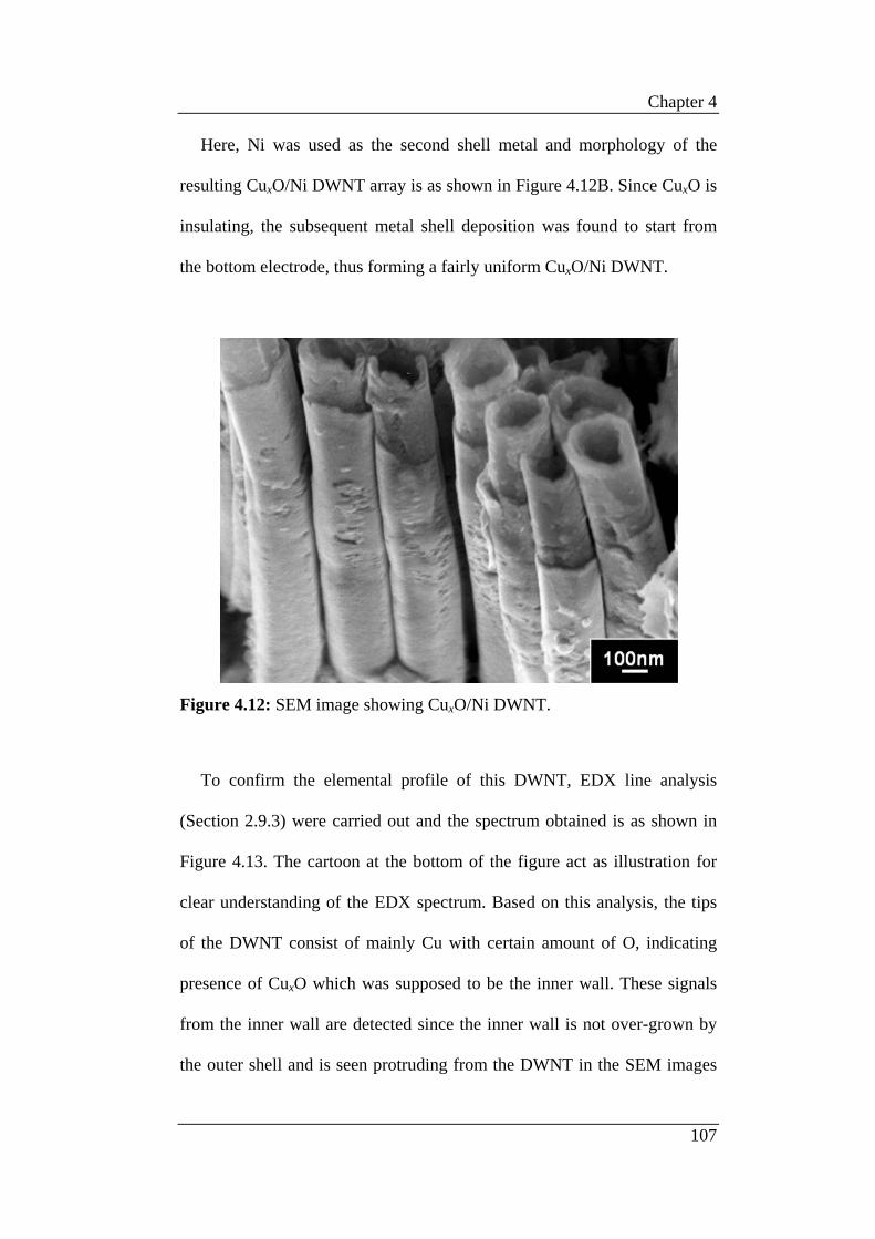
Chapter 4
107
Here, Ni was used as the second shell metal and morphology of the
resulting CuxO/Ni DWNT array is as shown in Figure 4.12B. Since CuxO is
insulating, the subsequent metal shell deposition was found to start from
the bottom electrode, thus forming a fairly uniform CuxO/Ni DWNT.
Figure 4.12: SEM image showing CuxO/Ni DWNT.
To confirm the elemental profile of this DWNT, EDX line analysis
(Section 2.9.3) were carried out and the spectrum obtained is as shown in
Figure 4.13. The cartoon at the bottom of the figure act as illustration for
clear understanding of the EDX spectrum. Based on this analysis, the tips
of the DWNT consist of mainly Cu with certain amount of O, indicating
presence of CuxO which was supposed to be the inner wall. These signals
from the inner wall are detected since the inner wall is not over-grown by
the outer shell and is seen protruding from the DWNT in the SEM images

Chapter 4
108
in both Figure 4.12B and Figure 4.13. Meanwhile, the outmost layer from
the root of the NTs shows signal of Ni, confirming the part grown as the
outer shell consists of Ni. This demonstrates the successful deposition of
CuxO/Ni DWNT via the “Pore Widening” method.
Figure 4.13: EDX line analysis of the CuxO/Ni DWNT, indicating a fairly uniform distribution of the metal and oxide.

Chapter 4
109
4.2 Summary
The versatility of “Pore Widening” method in creating various coaxial
multi-layered 1D hetero-nanostructures was successfully demonstrated.
Diluted H3PO4, which has been used to chemically remove the barrier layer
during the fabrication of AAO membrane, is advantageously used here to
generate an annular gap between the deposited core and the wall of AAO
nanochannel. The presence of this gap thus allows deposition of another
layer of material as the sheath, forming coaxial 1D hetero-nanostructure.
Besides, it was shown that the size of the annular gap and thus the
subsequent thickness of the shell, can be controlled by carefully tuning the
duration of pore-widening. This is of course limited by the thickness of the
AAO nanochannel walls.
Expanding from the architectures demonstrated here, we suggest that our
“Pore Widening” method can be used to fabricate coaxially multi-layered
NWs and NTs with varied combinations of materials. As in most AAO
template-assisted synthesis, the final core and shell components must be
inert to NaOH used to remove the template. Thus, in addition to Au, Cu, Ni
and PPy demonstrated in this report, other possible materials include
PANI,11 poly(p-phenylene vinylene),26, 27 silver,28 SiO2,16 ZnS,19 Bi and
Bi2O3.18 The additional limitation of “Pore Widening” method, of course, is
that the core or inner shell material must also be inert to dilute H3PO4. We
believe many polymeric materials are suitable in this aspect, as well as
most of the inert metals and elements. Hence, we envisage that many
interesting nanostructures can be generated using this “Pore Widening”

Chapter 4
110
approach which will be useful in potential functional devices in various
areas.
4.3 References
1. B. Z. Tian, X. L. Zheng, T. J. Kempa, Y. Fang, N. F. Yu, G. H. Yu,
J. L. Huang, C. M. Lieber. Nature 449 (2007) 885-890.
2. X. H. Xia, J. S. Luo, Z. Y. Zeng, C. Guan, Y. Q. Zhang, J. P. Tu,
H. Zhang, H. J. Fan. Sci. Rep. 2 (2012) 981.
3. C. Y. Yan, H. Jiang, T. Zhao, C. Z. Li, J. Ma, P. S. Lee. J. Mater.
Chem. 21 (2011) 10482-10488.
4. X. H. Xia, J. P. Tu, Y. Q. Zhang, X. L. Wang, C. D. Gu, X. B.
Zhao, H. J. Fan. ACS Nano 6 (2012) 5531-5538.
5. Y. C. Zhu, Y. Bando, D. F. Xue, F. F. Xu, D. Golberg. J. Am.
Chem. Soc. 125 (2003) 14226-14227.
6. X. G. Wen, S. H. Yang. Nano Lett. 2 (2002) 451-454.
7. J. Hwang, B. D. Min, J. S. Lee, K. Keem, K. Cho, M. Y. Sung, M.
S. Lee, S. Kim. Adv. Mater. 16 (2004) 422-425.
8. D. Li, Y. N. Xia. Nano Lett. 4 (2004) 933-938.
9. Q. Li, C. R. Wang. Appl. Phys. Lett. 82 (2003) 1398-1400.
10. Y. B. Li, Y. Bando, D. Golberg, Z. W. Liu. Appl. Phys. Lett. 83
(2003) 999-1001.
11. S. Y. Bae, H. W. Seo, H. C. Choi, D. S. Han, J. Park. J. Phys.
Chem. B 109 (2005) 8496-8502.

Chapter 4
111
12. N. I. Kovtyukhova, T. E. Mallouk, T. S. Mayer. Adv. Mater. 15
(2003) 780-785.
13. J. C. Bao, K. Y. Wang, Z. Xu, H. Zhang, Z. H. Lu. Chem.
Commun. (2003) 208-209.
14. L. Li, Y. W. Yang, G. H. Li, L. D. Zhang. Small 2 (2006) 548-553.
15. M. Lahav, E. A. Weiss, Q. B. Xu, G. M. Whitesides. Nano Lett. 6
(2006) 2166-2171.
16. W. R. Hendren, A. Murphy, P. Evans, D. O'Connor, G. A. Wurtz,
A. V. Zayats, R. Atkinson, R. J. Pollard. J. Phys.-Condes. Matter
20 (2008) 362203.
17. P. R. Evans, W. R. Hendren, R. Atkinson, R. J. Pollard. J.
Electrochem. Soc. 154 (2007) K79-K82.
18. G. E. Thompson, G. C. Wood. Nature 290 (1981) 230-232.
19. H. Masuda, K. Fukuda. Science 268 (1995) 1466-1468.
20. J. E. Mark, ed., Polymer data handbook, Oxford University Press,
New York, 2nd edn, 2009.
21. L. Li, Y. W. Yang, X. H. Huang, G. H. Li, R. Ang, L. D. Zhang.
Appl. Phys. Lett. 88 (2006) 103119.
22. X. C. Dou, G. H. Li, X. H. Huang, L. Li. J. Phys. Chem. C 112
(2008) 8167-8171.

Chapter 4
112

113
Chapter 5
Synthesis and Electrochemical Properties of
Cobalt/Aluminium Layered Double Hydroxides
Hierarchical Nanostructures
Layered double hydroxides (LDH) are a family of anionic clays
consisting of alternating stacking of positively charged brucite-type metal
hydroxide layers and negatively charged interlayer of counter-anions and
water molecules. The positive charge of the brucite-type layer is due to
partial isomorphous substitution of divalent metal cations by trivalent
cations. The general structure of an LDH is shown in Figure 5.1 and can be
defined by the general formula [MII1-xMIII
x(OH)2]x+(An-)x/n.mH2O, where
MII and MIII are the di- and trivalent metal ions and An- is the counter-
anion.1 Since the naturally occurring mineral hydrotalcite (HT)
Mg6Al2(OH)16CO3.4H2O belongs to this class of materials, LDH are also
commonly known as HT-like materials. The nature of MII, MIII, An- (e.g. Cl-,
SO42-, CO3
2-) and the value of the stoichiometric coefficient x can be
tailored to modulate the properties of LDH for various applications.2-5 The
only limitation is that the ionic radii of MII and MIII must not differ much
from those of Mg2+ and Al3+, respectively.1 In the subsequent paragraphs, a
particular LDH will be referred to using the short formula M(II)/M(III)-
LDH.

Chapter 5
114
Figure 5.1: General structure of a layered double hydroxide (LDH), with several parameters as defined. [Schematics redrawn and adapted from Ref. 1, 6]
Co/Al-LDH, with Co2+ as the MII ion and Al3+ the MIII ion, is among the
most commonly studied LDH, popular for its excellent electrochemical
properties.5, 7-10 The Co metal centre is responsible for the redox reaction
that gives the electrochemical properties of the material. The incorporation
of Al3+ was found to enhance the electrochemical properties of Co/Al-LDH
as compared to pure Co(OH)2, as it enables the electrochemical oxidation
of Co to higher oxidation state in a multi-electron process.11, 12 According
to Taube, octahedral Co(III) complexes are inert and inaccessible for rapid

Chapter 5
115
electron transfer due to their d6 low-spin configuration.13, 14 For Co/Al-
LDH, the octahedral symmetry of the Co ligands in the hydroxide layer is
deformed by the smaller and more highly charged Al3+ ion. In this way, the
Co(III) obtained from oxidation of Co(II) can be further oxidized to higher
oxidation state, i.e. Co(IV), resulting in an increase of specific energy in the
high potential range (where Co(III)/Co(IV) redox would occur) in addition
to that in the lower potential range (for Co(II)/Co(III) redox).7, 15, 16 This is
in contrast to that of pure Co(OH)2, where only the latter is observed.17, 18
Due to such improvement via the partial isomorphous substitution of Co2+
by Al3+, Co/Al-LDH has gained importance in the development of
electrochemical capacitors (ECs) and electrochemical sensors (ESs). We
will briefly review each of these applications in the followings.
ECs are power devices that can complement or replace batteries in the
energy storage field due to their fast charging time, high power delivery or
uptake in shorter times, long cycle life, excellent safety and eco-friendly
nature.19, 20 There are two categories of ECs which operate on different
mechanisms, namely, electric double-layer capacitors (EDLCs) and
pseudocapacitors. EDLCs store electrical charge at the interface between
the electrode and electrolyte. For pseudocapacitors, their capacitance arises
from Faradaic redox reactions taking place at the electrode/electrolyte
interface at an appropriate potential range. Comparing these two,
pseudocapacitors generally exhibit larger capacitance, energy density and
lower working voltage than EDLCs, since the Faradaic redox processes
could occur both on surface and in the bulk near the surface of the solid

Chapter 5
116
electrode.21-23 Ruthenium oxide (RuO2) has been one of the most promising
electrode materials for pseudocapacitors but it is too expensive for
commercial use.24 Recent development has found interests in using LDH as
a cheaper alternative but with higher capacitive performance.2, 5 With the
enhanced electrochemical properties via the incorporation of Al3+ and the
lower cost of Co,25 Co/Al-LDH has good potential as a cost-effective
electrode material for pseudocapacitor.7, 8
ESs are chemical sensors which give an electrical signal in response to
chemical reaction between the analyte and the electrode. The signal
obtained can arise from a change in current (amperometry), voltage
(potentiometry) or resistance (conductometry). Majority of the studies were
devoted to amperometric detection of glucose (Glc) that has great
importance in the diagnosis and treatment of diabetes mellitus, as well as in
monitoring and control of food processes. Various amperometric Glc
sensors based on glucose oxidase (GOx) enzyme have been investigated.26,
27 Despite the low detection limit, these enzymatic Glc sensors are often
unstable due to the intrinsic nature of the enzyme.28 This then leads to the
increased attention towards the development of non-enzymatic sensors,
which are more stable, simple, reproducible and free of oxygen limitation.28,
29 Electrodes made up of noble metals and their alloys have been explored
but they are too costly and prone to poisoning by chloride ions.
There is recently a growing trend of exploring LDH as a cheaper
alternative for Glc sensors.4, 5 LDH can either be used as host matrices to
immobilize enzyme or directly as redox catalyst that mediates the

Chapter 5
117
electrooxidation of Glc.4, 5 The latter is applicable as non-enzymatic Glc
sensors and the LDH used often contain redox-active metal centres such as
Ni(II) and Co(II),5 which are responsible for their electrocatalytic
behaviour in basic solution. There were only a few reports on the
application of Co/Al-LDH for electrochemical Glc sensing. Initial reports
showed that Co/Al-LDH is selective towards polyhydric compounds (e.g.
glycerol, Glc and sucrose) in the presence of alcohols, thus it can be used as
a complementary electrode to remove the signals from sugars for
determination of ethanol in beer samples.30, 31 Only recently, Co/Al-LDH
was applied to amperometric and colorimetric detection of Glc in serum
samples, but it was mainly focused on the latter.9
Nanotechnology is becoming increasingly important in the development
for ECs and ESs applications. The high surface area of nanostructured
materials such as nanoflakes (NFs), nanosheets (NSs) and nanowires (NWs)
can offer more active sites, better utilization of materials and rapid transfer
of electron and charge transport, all which can improve the performance of
ECs and ESs.28, 32-34 Hierarchical nanostructures, consisting of a
combination of nanostructures, were recently shown to enhance electrode
performance by further improving the surface area and also the efficiency
of charge transport.17, 35
In this Chapter, we demonstrate a direct synthesis of hierarchical
nanostructure of Co/Al-LDH NFs supported on Co NWs on conductive
substrate. These arrays of nanostructures are ready for use without the need
of binder, thus simplifying the electrode preparation process. Effect of

Chapter 5
118
various synthesis parameters and their electrochemical properties for
pseudocapacitor and Glc sensing will be presented in Section 5.2 and
Section 5.3, respectively.
5.1 Synthesis and characterizations of Co/Al-LDH hierarchical
nanostructures
Hierarchical Co/Al-LDH nanostructures were synthesized according to
details as described in Section 2.2.3. This simple procedure involves first
electrodepositing Co NWs into the AAO nanochannels followed by NaOH
alkaline treatment to remove the template and at the same time forming the
LDH as NFs on the Co NWs surfaces. The length of the Co NWs grown
within the AAO nanochannels can be readily controlled via
electrodeposition duration. The working linear correlation is demonstrated
in Figure 5.2 and, in this Chapter, Co NWs of about 5 μm prepared at 90
minutes were used throughout.

Chapter 5
119
Figure 5.2: Average length of Co NWs obtained as a function of electrodeposition duration.
After the alkaline treatment in 2.5 M NaOH, some NFs were observed
on both the top and sides of the Co NWs as shown in Figure 5.3. These NFs
could arise due to the corrosion of Co NWs in the concentrated alkaline
solution, leading to the precipitation of less soluble Co(OH)2.36 In the
presence of Al3+ arising from the dissolution of AAO template, some Al3+
could isomorphously substitute Co2+ during the hydroxide formation to the
final LDH NFs. Generally, it can be seen that more NFs were formed with
longer alkaline treatment time, especially on top of the NWs array.
Moreover, the NF crystals also became larger and the hexagonal shape
became more defined for prolonged alkaline treatment as shown from the
top views in the right panel of Figure 5.3.

Chapter 5
120
Figure 5.3: SEM images of Co/Al-LDH samples after alkaline treatment for (A) 1, (B) 18, (C) 24 and (D) 48 hours. The left and right panels show respectively the side and top views for each samples.

Chapter 5
121
In comparison to the top layer, NFs on the sides of the NWs are much
smaller in size and the hexagonal shapes less defined. The growth of larger
crystals may be restricted on the sides due to the density of the NWs as the
gap in between the NWs is less than 100 nm. Diffusion of NaOH to
replenish the depleted OH- ions would be much slower in these gaps than at
the top of the NWs.
EDX analysis (Section 2.9.3) confirmed that the NFs contain Al and
their content in atomic percentage ratio, i.e. x = Al / (Al + Co), are
estimated as given in Table 5.1. The Al in the NFs has to originate from the
Al3+ ions provided by the dissolution of the AAO template that is made up
of amorphous amphoteric alumina, Al2O3. Etching by alkaline solution can
be described by Equations 5.1 and 5.2:
2 NaOH + Al2O3 → 2 NaAlO2 + H2O (5.1)
NaAlO2 + 2 H2O → NaOH + Al(OH)3 (5.2)
With the presence of Al3+ ion in the alkaline solution, this ions can be
doped into the lattice of cobalt hydroxide during the hydroxide formation.
This is similar to the formation of HT-like Co/Al-LDH where some Co2+
are isomorphously substituted by Al3+ during the formation of cobalt
hydroxide in the presence of both Co2+ and Al3+ ions in the alkaline
solution.8

Chapter 5
122
From Table 5.1, we found that the Al content increases with the duration
of alkaline treatment but seems to reach a plateau after 24 hours of
treatment. Longer duration of treatment allows time for more Al3+ to be
integrated into the cobalt hydroxide, forming more Co/Al-LDH. The Al
content in the NFs would reach a constant either because the amount of
Al3+ was limited by the AAO template.
Table 5.1: Average atomic percentage obtained from EDX analyses of Co/Al-LDH samples for each alkaline treatment time.
Treatment time (hr) Co (at%) Al (at%) O (at%) Al content, x
[Al / (Al + Co)] 1 93.04 ± 0.93 0.62 ± 0.14 6.34 ± 0.90 0.01 ± 0.01
18 72.69 ± 2.77 6.78 ± 1.03 20.54 ± 1.80 0.09 ± 0.02
24 68.55 ± 1.04 8.30 ± 0.26 23.15 ± 1.09 0.11 ± 0.01
48 60.90 ± 1.44 8.62 ± 0.29 30.47 ± 1.26 0.12 ± 0.01
The formation of Co/Al-LDH was verified using XRD (Section 2.9.9)
and their diffraction patterns are given in Figure 5.4. Peaks characteristic of
metallic Au, Co and Cu are observed and these arise from the Au substrate,
Co NWs and Cu tape, respectively. Cu tape was used to hold the template
to the sample holder for analysis. Other than that, the XRD patterns match
well with characteristic peaks of Co6Al2CO3(OH)16.4H2O (JCPDS card no.
00-051-0045), indicating that our Co/Al-LDH nanostructures are
isomorphous with the hydrotalcitic phase of the reference. These peaks,
especially the (003) diffraction peak, became more intense at longer
duration of alkaline treatment. The increasing XRD peak intensities and the

Chapter 5
123
EDX Al content indicate that this LDH species is increasingly dominant on
the surface of our samples as treatment time increases. By referencing to
the standard XRD database, these samples may contain carbonate (CO32-)
as the interlayer anions in the LDH. This may be due to the presence of
carbon dioxide (CO2) gas in the solution during alkaline treatment.1, 15
Figure 5.4: XRD pattern of Co/Al-LDH samples prepared at the specified alkaline treatment time. Characteristic peaks for Co/Al-LDH are as labelled. Reference peaks: Au (JCPDS 01-071-4614), Co (JCPDS 01-071-4652), Cu (JCPDS 01-071-4611) and Co6Al2CO3(OH)16·4H2O (JCPDS 00-051-0045).
In the following sections, we investigate the applications of these unique
Co/AL-LDH NFs on Co NWs structures as pseudocapacitors and sensors.
For ease of discussion, we will label these electrodes as Co/Al-NWNF-y,

Chapter 5
124
with y being the hours of alkaline treatment time during sample preparation.
From Table 5.1 and the above discussion, it should be noted that the Al
content, or the amount of Co/Al-LDH NFs, increases with y in these
samples.
5.2 Electrochemical capacitance of Co/Al-LDH hierarchical
nanostructures
The electrochemical behaviour of these Co/Al-NWNF nanostructures for
application as EC was first studied via cyclic voltammetry (CV) and
galvanostatic charge-discharge (C-D) measurements (Section 2.6). Typical
CV curves scanned at 10 mV/s in 1 M KOH for samples prepared at
various alkaline treatment time are shown in Figure 5.5. All the curves
show two sets of redox peaks (labelled as I/I’ and II/II’) that are due to the
Faradaic reactions as shown in Equation 5.3 and 5.4, respectively.7
Co(OH)2 + OH- CoOOH + H2O + e- (5.3)
CoOOH + OH- CoO2 + H2O + e- (5.4)
Initially when the sample was alkaline-treated for 1 hour (Co/Al-NWNF-1),
the Faradaic current for redox I/I’ at lower potential range (-0.05 V to 0.1 V)
is larger than that for redox II/II’ (0.2 V to 0.5 V). The CV profile for
Co/Al-NWNF-18 shows a reversing trend, however, as the Faradaic current
for redox II/II’ begin to increases. The current for redox II/II’ further

Chapter 5
125
increases while that for redox I/I’ decreases significantly for Co/Al-NWNF-
24 and Co/Al-NWNF-48.
Figure 5.5: CV curves at scan rate of 10 mV/s for Co/Al-NWNF electrodes in 1 M KOH electrolyte. Samples prepared at varying alkaline treatment time are compared.
These CV curves suggest that Al content in the NFs has significant
effect on the capacitance at high potential range. This observation is similar
to that reported by Gupta et al. for their Al-substituted α-cobalt hydroxide
nanosheet film.7 As mentioned, the incorporation of Al3+ would distort the
octahedral symmetry of Co ligands, enabling the supposedly inert Co(III)

Chapter 5
126
sites to be further oxidized to Co(IV). This thus increases the capacitance in
the high potential range.11, 12
The respective charge-discharge (C-D) curves for the Co/Al-NWNF
samples at 2.5 mA/cm2 in 1M KOH are shown in Figure 5.6. All curves
show the near symmetrical triangular shape, suggesting good
supercapacitive behaviour. Similarly, it was observed that the capacitance
at high potential range also increases with the increase in Al content.
Figure 5.6: C-D curves at 2.5 mA/cm2 current density for Co/Al-NWNF electrodes in 1 M KOH electrolyte. Samples prepared at varying alkaline treatment time are compared.

Chapter 5
127
From these discharge curves, area-specific capacitance (Ca) can be
calculated using Equation 5.5:
VtI
C da ∆
∆= (5.5)
where Id (A/cm2) is the discharge current density, ∆t (s) is the discharge
time and ∆V (V) is the discharge potential range. Thus, Ca for each Co/Al-
NWNF electrode obtained at various current densities were calculated and
plotted in Figure 5.7, together with their corresponding Al content. It is
clearly seen from both plots that Ca and the Al content increase with the
alkaline treatment time in the same way, indicating that the enhancement of
capacitance is correlated to the formation of Co/Al-LDH NFs. The largest
capacitance of 0.510 F/cm2 is obtained from Co/Al-NWNF48, containing
12% Al, measured at current density of 2.5 mA/cm2.
Based on Figure 5.7, all our Co/Al-NWNF electrodes were found to
have similar high-rate capability compared to each other, preserving about
66% of the capacitance at 2.5 mA/cm2 when the current density is increased
to 12.7 mA/cm2. One aspect that could affect the high-rate capability is the
electrode resistance. It was reported for Co/Al-LDH film, however, that
increasing Al content in would decrease the high-rate capability because
the non-electroactive Al increases the internal resistance of the electrode.8
Our samples are thus unique as the high-rate capability is unaffected by the
Al content. We believe that in our case, the probable increase of resistance
is offset by an improved electron transport due to the hierarchical geometry
of Co/Al-LDH NFs supported on Co NWs grown on gold current

Chapter 5
128
collector.17 The NWs allow a direct electron path from the NFs to the
current collector and thus provide a facile electron path for charge transport,
reducing the electrode resistance.
Figure 5.7: Correlation for Al content and area-specific capacitance at varying current densities against alkaline treatment time.
Coulombic efficiency or charge/discharge efficiency is the efficiency
where charge is transferred or transported in a system. This can be
estimated using the equation: η = td/tc x 100%, where td and tc are the
discharge and charge time in seconds, respectively. The coulombic
efficiencies for all samples at each current density are thus calculated and
plotted as shown in Figure 5.8. For the Co/Al-NWNF-48 sample, the
efficiency dropped from 97% to 89% whereas for Co/Al-NWNF-1 sample,

Chapter 5
129
the value dropped from 97% to 74%. This shows that samples treated at
longer duration (which contain high amount of Al) have better reversibility
at large current density than those at shorter treatment time (which contain
low amount of Al).
Figure 5.8: Coulombic efficiency against current density for samples at varying alkaline treatment time. Inset: cycle life data at 12.7 mA/cm2.
The electrochemical stability of our Co/Al-NWNF samples was tested
and the result is shown in the inset of Figure 5.8. All electrodes were
subjected to 3000 continuous C-D cycles at 12.7 mA/cm2 in 1 M KOH
within potential range of 0 V to 0.45 V. Good cycling life was observed
regardless of the alkaline treatment time or Al content in the NFs. After

Chapter 5
130
3000 cycles, the capacitance was retained at more than 90% of their
original capacitance, showing excellent electrochemical stability.
Numerous studies on using Co/Al-LDH as the electrode material for
pseudocapacitor were reported since the last decade.7, 8, 35, 37-40 EC
performances of a few examples are tabulated in Table 5.2. However, fair
comparison is extremely difficult among these literature studies since
electrode performance is dependent on experimental conditions such as the
type of electrolyte, electrolyte pH, electrode matrix and type of current
collectors. Comparatively, our Co/Al-NWNF electrodes exhibit several
merits such as large capacitance and good electrochemical stability.
Table 5.2: Examples of Co/Al-LDH-based electrodes reported in the literatures and their EC performances.
Electrode Material / Current Collector
Method Cm (F/g)
Ca (F/cm2)
Rate capabi-
lity
Cycle life
(cycle no.)
Ref.
Co/Al-NWNF-48 / Au
GS (2.5 mA/cm2, 0-0.45V vs Ag/AgCl 3M
KCl in 1M KOH) - 0.510 66 % 92%
(3000) This study
Co0.92-Al0.08 LDH / SS
GS (1 A/g, 0-0.4V vs Ag/AgCl sat. KCl in 1M
KOH) 843 0.176* - - 7
Co0.75-Al0.25 LDH / ITO
GS (1.3 A/g, 0-0.55V vs Hg/HgO in 6M KOH) 833 0.046* - 95 %
(2000) 8
Co/Al-LDH / Ni foam
GS (60 mA/g, -0.15-0.55V vs Hg/HgO in 6M
KOH) 684 13.68* - 80 %
(1000) 38
Co/Al-LDH / Ni foam
GS (2 A/g, -0.1-0.5V vs SCE in 1M KOH + 0.1M
K3Fe(CN)6) 712 - -
67.0 %
(200) 40
MnO2-CoAl LDH / CFs
GS (1 A/g, -0.2-0.6V vs Hg/HgO in 1M LiOH) 944 1.153* 64.6 % 98.2%
(6000) 35
* Values calculated based on details of setup as described in the literature. SS: stainless steel, ITO: Indium-doped tin oxide, CFs: carbon fibers, GS: Galvanostatic charge-discharge.

Chapter 5
131
5.3 Electrochemical glucose sensing of Co/Al-LDH hierarchical
nanostructures
Other than electrochemical capacitor, Co/Al-LDH was also studied for
its electrocatalytic behaviour applicable as electrochemical sensor. In this
Section, we investigated the electrocatalytic activity of Co/Al-NWNF-1 and
Co/Al-NWNF-24 electrodes towards Glc oxidation for potential application
as amperometric non-enzymatic Glc sensor.
Firstly, the electrocatalytic activity of the electrodes towards oxidation
of Glc in alkaline solution was analyzed using CV (Section 2.7). CV curves
of the two electrodes at scan rate of 10 mV/s in the absence and increasing
amount of Glc in 0.1 M NaOH are shown in Figure 5.9A. In this electrolyte,
both electrodes showed two redox couples (labelled as I/I’ and II/II’) that
are related to the process Co(II)/Co(III) and Co(III)/Co(IV), which appear
to be overlapping. This overlapping of peaks is similarly observed for the
Co/Al-LDH films deposited on indium tin oxide (ITO) substrate by
Scavetta et al.9 Upon the addition of Glc, current increase at redox couple
II/II’ is found to be higher than that at I/I’. This confirms that the
electrooxidation of Glc in alkaline solution at our Co/Al-NWNF electrodes
is mainly mediated by the Co(III)/Co(IV) redox couple, similar to other
works on Co and Ni-based electrochemical Glc sensors.9, 41, 42 The Co(III)
centres can act as redox mediators for Glc oxidation according to the
following equations and the mechanism is illustrated by the cartoon shown
in Figure 5.9B:9

Chapter 5
132
Co(III)-LDH + OH- Co(IV)-LDH(OH-) + e- (5.6)
Co(IV)-LDH(OH-) + Glc Co(III)-LDH + OH- + gluconolactone (5.7)
Based on Equation 5.7, Co(IV) centres would be consumed and reduced to
give more Co(III) in the presence of Glc. Reaction as shown in Equation
5.6 would be pushed forward, resulting in enhancement of anodic peak for
II/II’ redox as reflected in the CV curves in Figure 5.9A.

Chapter 5
133
Figure 5.9: (A) CV curves at 10 mV/s in the absence and increasing amount of glucose (Glc) in 0.1 M NaOH solution. Dashed and solid lines are for Co/Al-NWNF-1 and Co/Al-NWNF-24 samples, respectively. (B) A cartoon showing the electrooxidation of glucose on Co/Al-LDH NFs grown on Co NWs.

Chapter 5
134
Since the electrooxidation of Glc at both electrodes is more pronounced
at region after 0.25 V, applied potentials of 0.3 V and 0.4 V were chosen to
conduct the amperometric Glc sensing measurements (Section 2.7). Figure
5.10 shows rapid and stable current response upon the successive addition
of Glc for both electrodes. As expected from observations derived from CV
curves (Figure 5.9A), the increase of current upon addition of Glc is larger
at 0.4 V than at 0.3 V. Comparing the two electrodes at the same applied
potential, Co/Al-NWNF-24 gives rise to larger current response than that
for Co/Al-NWNF-1. However, as the total Glc concentration in the
electrolyte increases with further addition, the current responses gradually
decrease. This is most probably due to higher tendency of the analyte and
electrocatalytic reaction intermediates to adsorb onto the active sites of the
electrode, thus hindering the catalytic activities and leads to a reduction in
current response. Consequently, this would affect the linear range of the
electrodes at each applied potential as will be discussed in the following
paragraph.

Chapter 5
135
Figure 5.10: Amperometric response upon the successive addition of Glc in 0.1 M NaOH at the respective applied potential for Co/Al-NWNF-1 and Co/Al-NWNF-24. Inset: The corresponding calibration curves. [Note: The dilution effect has been taken into consideration for all concentration values indicated]
From the chronoamperograms, current vs. Glc concentration calibration
plots are generated as shown in the inset of Figure 5.10. The corresponding
linear range of these calibration plots are expanded more clearly in Figure
5.11. Equations for the linear regression of each calibration curve are given
as indicated in the Figure. From the slopes of these curves, it is found that
measurement at 0.4 V gives higher sensitivity than 0.3 V. Though more
sensitive, measurement at 0.4 V resulted in smaller limit of linearity (LOL)
(up to only 0.6 mM Glc) for both electrodes. At this larger applied potential,
more Glc molecules would be oxidized and produce more intermediates,

Chapter 5
136
leading to the higher current response at each Glc addition (i.e. higher
sensitivity). But, this would also cause the adsorption of analyte or
intermediate molecules onto the active sites as mentioned in the preceding
paragraph to occur at much lower concentration than when lower potential
(0.3 V) was applied, resulting in the observed smaller LOL. Larger LOL is
observed at 0.3 V up to 2.40 mM for Co/Al-NWNF-1 and 1.60 mM for
Co/Al-NWNF-24 but at the expense of sensitivity dropping to 68.7 and
188.8 µAmM-1cm-2, respectively.
Figure 5.11: Expanded region of linear range from the calibration curve in the inset of Figure 5.10.

Chapter 5
137
At each applied potential, Co/Al-NWNF-24 is always more sensitive to
the detection of Glc than Co/Al-NWNF-1. This may be because the surface
of Co/Al-NWNF-24 electrode consists of predominantly Co/Al-LDH
species and NFs. Due to the layered structure of Co/Al-LDH, there is a
large interlayer spacing in between the hydroxide layers.1 At the chosen
applied potential, Co(III) centres would be oxidized to Co(IV) as described
by Equation 5.6 and OH- ions would diffuse from the electrolyte to the
surface of active material to ensure electroneutrality. With larger interlayer
spacing, OH- ions easily diffuse into the electrode surface of our Co/Al-
NWNF electrodes. Thus. Equation 5.6 will shift to the right and more
catalytic-active Co(IV) sites would be generated for the electrooxidation of
Glc (Equation 5.7).
A comparison of the Glc sensing performance of our electrodes and
some recently reported Co-based electrodes are tabulated in Table 5.3.
Comparatively, our electrodes exhibit several merits such as high
sensitivity even at low applied potential and relatively high LOL than most
of the electrodes. The only one report that is also based on Co/Al-HT film9
is comparatively less sensitive than our Co/Al-NWNF-24 electrode, even
when their measurement was performed at higher applied potential. We
would attribute the higher performance of our electrodes to the higher
surface area arising from the hierarchical nanostructures designed.

Chapter 5
138
Table 5.3: A comparison of non-enzymatic Glc sensing performance of Co-based electrodes in the literature.
Electrode materials
E (V vs Ag/AgCl)
Sensitivity (µA
mM-1cm-2)
LODa (µM)
LOLb (mM)
Resp. time (s)
Ref.
Co/Al-NWNF-1 (0.1 M NaOH)
0.30 68.7 34.7 2.40
≤ 6c This study
0.40 385.0 16.8 0.60
Co/Al-NWNF-24 (0.1 M NaOH)
0.30 188.8 30.5 1.60
0.40 543.0 17.3 0.60
Co/Al HT film (0.1 M NaOH)
0.50 (vs SCE) 424.0 2.0 1.50 - [9]
Co3O4 NFs (0.1 M NaOH) 0.59 36.25 0.97 2.04 < 7 [42]
Co3O4 NRs
(1.0 M NaOH) 0.50 571.8 0.058 3.50 - [43]
CoOOH nanosheets (0.1 M NaOH)
0.40 341.0 30.9 0.70 < 4 [44]
0.50 967.0 10.6 0.50 a LOD = Limit of detection (S/N = 3); b LOL = Limit of linearity; c Response to 0.5 mM Glc
With OH- ions directly involved in Equation 5.6, concentration of NaOH
(also pH of the electrolyte) would have an effect on the electrooxidation of
Glc in Equation 5.7. As shown in Figure 5.12, it is obvious that the current
response to a constant Glc concentration of 4 mM generally increases with
the NaOH concentration and pH values. This dependency of
electrocatalytic activity on the OH- ion concentration is similar to other
reports on Co and Ni-based Glc sensors.41, 43-45 As mentioned in the
previous paragraph, OH- ions would have to diffuse from the electrolyte

Chapter 5
139
into the surface active material to ensure electroneutrality after the Co(III)
centres in the hydroxide layers are oxidized to Co(IV). At higher OH-
concentration, more OH- is available as counter ion. Equation 5.6 will shift
to the right, generating more catalytic-active Co(IV) sites for
electrooxidation of Glc and thus better sensitivity.
Figure 5.12: Amperometric response of Co/Al-NWNF electrodes to 4 mM Glc at 0.3 V in electrolytes of varying NaOH concentration and pH values.
Comparing the two electrodes, the increased sensitivity with NaOH
concentration and pH of electrolyte was found to be more significant for
Co/Al-NWNF-24. As mentioned in Section 5.1, the main difference
between Co/Al-NWNF-1 and Co/Al-NWNF-24 is the nature of the
dominant surface active material, presumably Co NWs and Co/Al-LDH

Chapter 5
140
NFs for respective electrodes. At the same NaOH concentration, OH- ions
would diffuse more easily into the interlayer of Co/Al-LDH than for Co
due to the larger spacing of the interlayer.1, 46 Hence, the electrode surface
of Co/Al-NWNF-24 is activated to larger extent, leading to much higher
sensitivity towards Glc.
Since the current response arises due to Equation 5.7, any compounds
other than Glc that can be oxidized would interfere with the measurement.
In view of their potential applications as Glc sensor for blood/serum
samples, the selectivity of our electrodes were tested against naturally
occurring interfering compounds such as uric acid (UA) and ascorbic acid
(AA). The tests were carried out at 0.3 V to measure 4 mM Glc against
0.33 mM of UA and 0.125 mM of AA. These concentrations are similar to
that of normal physiological levels.47, 48 As shown in Figure 5.13, Co/Al-
NWNF-24 demonstrates better selectivity against UA and AA than Co/Al-
NWNF-1. The presence of UA and AA in the electrolyte with 4 mM Glc
resulted in only 3% and 4% increase of current response for Co/Al-NWNF-
24 but for Co/Al-NWNF-1, the increase was 30% and 13%, respectively.

Chapter 5
141
Figure 5.13: Amperometric response of Co/Al-NWNF electrodes to 4 mM Glc at 0.3 V in the presence of interfering compounds (UA: uric acid, AA: ascorbic acid) in 0.1 M NaOH electrolyte.
The selectivity towards Glc against UA and AA at our Co/Al-NWNF
electrodes may arise from the repelling effect as described by Ding et al.42
Since both Co/Al-NWNF electrodes in nature are hydroxides in the alkaline
electrolyte and their isoelectric points (IEP) occur at about pH 9.8 - 10.8,49-
51 their surfaces should be negatively charged in the 0.1 M NaOH
electrolyte (pH 12.9) used here. This negatively charged surface would then
repel UA and AA which are also negatively charged in the alkaline
environment due to the loss of proton. Based on such hypothesis, both
Co/Al-NWNF-1 and Co/Al-NWNF-24 should have similar selectivity
towards Glc. Instead, the Co/Al-NWNF-24 was observed to have better

Chapter 5
142
selectivity. This may be due to higher Al content integrated in Co/Al-
NWNF-24 electrode which may further enhance the negative charge of the
electrode surface as the IEP for Al occurs at pH 5.4,52 leading to larger
repelling effect against UA and AA. This demonstrates the potential of
Co/Al-NWNF-24 as a sensitive and selective non-enzymatic sensor for Glc
detection in blood/serum samples.
The reproducibility and stability of both electrodes were also
investigated. All measurements were carried out at 0.3 V in 0.1 M NaOH.
Both Co/Al-NWNF-1 and Co/Al-NWNF-24 electrodes showed good intra-
electrode reproducibility from five repeated measurements of 0.4 mM Glc
(n = 5) with relative standard deviation (RSD) of 2.0% and 2.9%,
respectively. However, the inter-electrode reproducibility in response to 0.4
mM Glc for three electrodes prepared at same synthesis conditions (n = 3)
is only satisfactory. Considerably low RSD of 14.7% and 18.2% were
observed for Co/Al-NWNF-1 and Co/Al-NWNF-24, respectively. Both
electrodes were found to have good stability. After 13 days of storage in
ambient condition, current responses for 0.4 mM Glc at Co/Al-NWNF-1
and Co/Al-NWNF-24 electrodes were found to preserve 96% and 94% of
their initial responses, respectively.
5.4 Summary
Hierarchical nanostructure of Co/Al-LDH NFs supported on Co NWs
was successfully fabricated through an alkaline treatment of Co NWs
embedded in AAO at ambient condition. These nanostructures were grown

Chapter 5
143
on current collector, thus can be used directly as electrode without the need
of binder and tedious electrode preparation procedures such as dispersion,
sonication, drop-casting and drying. The content of Al in NFs was found to
increase with the duration of alkaline treatment and the crystal structure
matched well with HT-like Co6Al2CO3(OH)16.4H2O.
The electrochemical capacitor properties of these Co/Al-LDH
nanostructured electrodes were found to improve with higher Al content
and when Co/Al-LDH is the dominant species on the electrode surface. In
addition to high capacitance value, these electrodes also show good rate
capability and coulombic efficiency, and excellent electrochemical stability.
For the application in non-enzymatic Glc sensor, our nanostructured
electrodes exhibited high sensitivity and low detection limit, with the
highest value of 543.0 µAmM-1cm-2 achieved at applied potential of 0.40 V.
These electrodes also exhibited good selectivity towards Glc in the
presence of uric acid and ascorbic acid, making this electrode a potential
sensitive and selective non-enzymatic sensor for Glc detection in
blood/serum samples.
5.5 References
1. F. Cavani, F. Trifiro, A. Vaccari. Catal. Today 11 (1991) 173-301.
2. X. X. Guo, F. Z. Zhang, D. G. Evans, X. Duan. Chem. Commun.
46 (2010) 5197-5210.
3. H. Abdolmohammad-Zadeh, Z. Rezvani, G. H. Sadeghi, E. Zorufi.
Anal. Chim. Acta 685 (2011) 212-219.

Chapter 5
144
4. D. Tonelli, E. Scavetta, M. Giorgetti. Anal. Bioanal. Chem. 405
(2013) 603-614.
5. C. Mousty, F. Leroux. Recent Patents on Nanotechnology 6 (2012)
174-192.
6. V. Rives, M. A. Ulibarri. Coord. Chem. Rev. 181 (1999) 61-120.
7. V. Gupta, S. Gupta, N. Miura. J. Power Sources 177 (2008) 685-
689.
8. Y. Wang, W. Yang, C. Chen, D. G. Evans. J. Power Sources 184
(2008) 682-690.
9. E. Scavetta, B. Ballarin, D. Tonelli. Electroanalysis 22 (2010)
427-432.
10. I. Gualandi, A. G. Solito, E. Scavetta, D. Tonelli. Electroanalysis
24 (2012) 857-864.
11. D. H. Buss, J. Bauer, W. Diembeck, O. Glemser. J. Chem. Soc.,
Chem. Commun. (1985) 81-82.
12. J. Bauer, D. H. Buss, H. J. Harms, O. Glemser. J. Electrochem.
Soc. 137 (1990) 173-178.
13. H. Taube. Adv. Inorg. Chem. 1 (1959) 1-53.
14. L. E. Orgel. An Introduction to Transition-Metal Chemistry:
Ligand-Field Theory. 2nd ed., Methuen & Co. Ltd., London (1966)
pp. 107-116.
15. E. Scavetta, B. Ballarin, M. Gazzano, D. Tonelli. Electrochim.
Acta 54 (2009) 1027-1033.
Chapter 5
145
16. E. Scavetta, B. Ballarin, C. Corticelli, I. Gualandi, D. Tonelli, V.
Prevot, C. Forano, C. Mousty. J. Power Sources 201 (2012) 360-
367.
17. C. Y. Yan, H. Jiang, T. Zhao, C. Z. Li, J. Ma, P. S. Lee. J. Mater.
Chem. 21 (2011) 10482-10488.
18. L. R. Hou, C. Z. Yuan, L. Yang, L. F. Shen, F. Zhang, X. G.
Zhang. Crystengcomm 13 (2011) 6130-6135.
19. J. R. Miller, P. Simon. Science 321 (2008) 651-652.
20. B. E. Conway. Electrochemical Supercapacitors: Scientific
Fundamentals and Technological Application. Plenum Press, New
York (1999).
21. Y. Zhang, H. Feng, X. B. Wu, L. Z. Wang, A. Q. Zhang, T. C. Xia,
H. C. Dong, X. F. Li, L. S. Zhang. Int. J. Hydrogen Energy 34
(2009) 4889-4899.
22. B. E. Conway, V. Birss, J. Wojtowicz. J. Power Sources 66 (1997)
1-14.
23. G. P. Wang, L. Zhang, J. J. Zhang. Chem. Soc. Rev. 41 (2012)
797-828.
24. H. Lee, M. S. Cho, I. H. Kim, J. D. Nam, Y. Lee. Synth. Met. 160
(2010) 1055-1059.
25. P. C. K. Vesborg, T. F. Jaramillo. RSC Adv. 2 (2012) 7933-7947.
26. B. J. Plowman, S. K. Bhargava, A. P. O'Mullane. Analyst 136
(2011) 5107-5119.
Chapter 5
146
27. D. W. Kimmel, G. LeBlanc, M. E. Meschievitz, D. E. Cliffel. Anal.
Chem. 84 (2012) 685-707.
28. P. Si, Y. J. Huang, T. H. Wang, J. M. Ma. RSC Adv. 3 (2013)
3487-3502.
29. G. F. Wang, X. P. He, L. L. Wang, A. X. Gu, Y. Huang, B. Fang,
B. Y. Geng, X. J. Zhang. Microchimica Acta 180 (2013) 161-186.
30. E. Scavetta, D. Tonelli. Electroanalysis 17 (2005) 363-370.
31. E. Scavetta, B. Ballarin, M. Berrettoni, I. Carpani, M. Giorgetti, D.
Tonelli. Electrochim. Acta 51 (2006) 2129-2134.
32. A. S. Arico, P. Bruce, B. Scrosati, J. M. Tarascon, W. Van
Schalkwijk. Nat. Mater. 4 (2005) 366-377.
33. J. Huang, T. Lei, X. Wei, X. Liu, T. Liu, D. Cao, J. Yin, G. Wang.
J. Power Sources 232 (2013) 370-375.
34. Q. F. Wang, X. F. Wang, B. Liu, G. Yu, X. J. Hou, D. Chen, G. Z.
Shen. J. Mater. Chem. A 1 (2013) 2468-2473.
35. J. W. Zhao, Z. Z. Lu, M. F. Shao, D. P. Yan, M. Wei, D. G. Evans,
X. Duan. RSC Adv. 3 (2013) 1045-1049.
36. A. Groysman. Corrosion for Everybody. Springer, (2010).
37. L.-H. Su, X.-G. Zhang. J. Power Sources 172 (2007) 999-1006.
38. Y. Wang, W. Yang, S. Zhang, D. G. Evans, X. Duan. J.
Electrochem. Soc. 152 (2005) A2130-A2137.
39. L. H. Su, X. G. Zhang, C. H. Mi, Y. Liu. J. Power Sources 179
(2008) 388-394.

Chapter 5
147
40. L. H. Su, X. G. Zhang, C. H. Mi, B. Gao, Y. Liu. Physical
Chemistry Chemical Physics : PCCP 11 (2009) 2195-2202.
41. L. Q. Luo, F. Li, L. M. Zhu, Y. P. Ding, Z. Zhang, D. M. Deng, B.
Lu. Colloids and Surfaces B: Biointerfaces 102 (2013) 307-311.
42. Y. Ding, Y. Wang, L. A. Su, M. Bellagamba, H. Zhang, Y. Lei.
Biosens. Bioelectron. 26 (2010) 542-548.
43. C. W. Kung, C. Y. Lin, Y. H. Lai, R. Vittal, K. C. Ho. Biosens.
Bioelectron. 27 (2011) 125-131.
44. K. K. Lee, P. Y. Loh, C. H. Sow, W. S. Chin. Electrochem.
Commun. 20 (2012) 128-132.
45. J. Yang, W. D. Zhang, S. Gunasekaran. Electrochim. Acta 56
(2011) 5538-5544.
46. A. W. Hull. Phys. Rev. 17 (1921) 571-588.
47. S. Park, H. Boo, T. D. Chung. Anal. Chim. Acta 556 (2006) 46-57.
48. S. Hrapovic, J. H. T. Luong. Anal. Chem. 75 (2003) 3308-3315.
49. Z. Z. Xu, Z. L. Chen, C. Joll, Y. Ben, J. M. Shen, H. Tao. Catal.
Commun. 10 (2009) 1221-1225.
50. K. Jurkiewicz. Int. J. Miner. Process. 17 (1986) 67-81.
51. G. A. Parks. Chem. Rev. 65 (1965) 177-198.
52. G. Lefevre, L. Cerovic, S. Milonjic, M. Fedoroff, J. Finne, A.
Jaubertie. J. Colloid Interface Sci. 337 (2009) 449-455.

Chapter 5
148

149
Chapter 6
Synthesis and Photocurrent Study of Aligned
MWCNT/PPV Core-shell Nanowires
The discovery of carbon nanotubes (CNT)1 have sparked new research
interests towards 1D nanostructures. CNT has high surface area and high
electrical conductivity, as well as unique thermal and mechanical
properties.2-6 Since then, composites of CNT with various polymers began
to sprout in order to attain synergistic effects of the combined materials,
mostly aimed at exploiting the unique mechanical properties of CNT.7
Subsequently, interests in their electronic properties began to grow with the
development of conjugated polymers (CPs) that exhibit unique electronic
and optical properties.8-10 Combination of these two materials are
promising for electronic and optoelectronic devices where improvement
such as higher electrical conductivity, electroluminescence efficiency and
photoconduction have been observed.11-16 These were attributed to the
ability of CNT in providing direct pathways for charge transport, which
enhanced conductivity and electroluminescence, and for separation of
excitons, which improved photoconductivity.
The CNT/CP composites can be in the form of (1) films where loose
strands of CNT are mixed within CP matrices,11-14 (2) compact membranes
consisted of individual CNT/CP core-shell NWs15,17 and (3) free-standing
arrays of perpendicularly aligned CNT/CP core-shell NWs on substrates.16,

Chapter 6
150
18, 19 Each of these has their disadvantages but all showed improvement of
properties compared to individual components. Nevertheless, those in the
form of core-shells were found to give additional advantage of higher
surface area. With the CP wrapping around each strands of CNT, the CNT
not only act as support that increases surface area of CP but also provide
direct pathways for charge transport.15-19 Besides, these CNT/CP core-shell
NWs can be grown on or transferred onto a conductive substrate, thus the
resulting product can be directly used as electrode without the need for
binder and this thus simplifies the electrode preparation process.
Much effort had been dedicated to explore simple synthesis method to
fabricate CNT/CP core-shell NWs such as surfactant-directed20, 21 and
ultrasonic-assisted15, 22 in-situ polymerization, water/oil microemulsion23
and electrochemical polymerization.16-19 Among these methods,
electrochemical polymerization may be the easiest with more control over
the polymer shell thickness via the adjustment of electrodeposition
parameters. Besides, this is one of the most commonly used methods for
deposition of CP shells onto arrays of “aligned” CNT.16, 18, 19
Poly(p-phenylene vinylene) (PPV), which was studied in Chapter 3, is
one of the CP that is popular for its optical and optoelectronic properties.
Composites of CNT with PPV were explored, mostly based on films where
loose strands of CNT are mixed within the PPV matrix.11, 12 The closest
form of CNT/PPV core-shell nanostructures are that reported by Kim et
al.24 and Massuyeau et al.25 The former was in the form of bilayer NTs
consisting of PPV inner layer and carbonized-PPV outer layer. No CNT

Chapter 6
151
was involved but they reported that the carbonized-PPV exhibits similar
electrical conductivity properties. For the latter, many strands of single-
walled CNT were embedded in each strand of PPV NWs within the
nanochannels of AAO.
In this Chapter, we aimed to study composite of PPV with free-standing
arrays of aligned multi-walled CNT (MWCNT) in the form of coaxial
MWCNT/PPV core-shell NWs. Hence, array of perpendicularly aligned
MWCNT produced by plasma-enhanced chemical vapour deposition
(PECVD) is used as template for PPV to deposit onto as the shell.
Preparation conditions for the electrodeposition of PPV shell are adapted
from those established in Chapter 3. Current-voltage (I-V) behaviour and
photocurrent (PC) response of these arrays of MWCNT/PPV core-shell
NWs will be studied and compared to that for MWCNT arrays.
6.1 Synthesis and characterizations of aligned MWCNT/PPV
core-shell nanowires
The free-standing arrays of aligned MWCNT and MWCNT/PPV core-
shell NWs were synthesized following details given in Section 2.3. Shown
in Figure 6.1 are the representative SEM images of the as-grown aligned
MWCNT arrays on n-type Si substrate. Although the strands of MWCNT
are not standing straight in rigid form, it was generally grown upward
perpendicularly from the substrate. The average diameter of the MWCNT
obtained is 21 ± 6 nm.

Chapter 6
152
Figure 6.1: (A) Low and (B) high magnification of side view SEM images of aligned MWCNT arrays as-grown via PECVD.
As a start, electrodeposition of PPV onto the MWCNT was carried out
at constant potential of -2.34 V, which was the optimized parameter used in
Chapter 3. As shown in Figure 6.2, a thick layer of PPV was formed on top
of the MWCNT array. On the other hand, the diameters of the MWCNT
remained small indicating that PPV was not successfully deposited as the
shell. The problem may arise from the rapid and continuous reduction of
TBX precursor to form PPV at the electrode-electrolyte interface when
constant potential was applied. Besides, “point effect” may have occurred
where deposition occurs faster at the tips of MWCNT and block the

Chapter 6
153
diffusion of precursor into the array, preventing deposition of PPV along
the sides of MWCNT.
Figure 6.2: SEM images of MWCNT/PPV obtained via electrodeposition at constant potential of -2.34 V for total charge of 0.5 C at (A) low and (B) high magnification. The white box in (A) indicates area where image (B) was obtained.
For better control of the deposition of PPV around the MWCNT and its
thickness, pulse potentiometry was explored. In principle, this technique
enables slow “layer-by-layer” deposition, and can result in more controlled
growth than constant potential.26, 27 There was no specific rule for the best
pulse parameters28 and Figure 6.3 illustrates one cycle of the square-wave
pulsed-potential sequence optimized for the deposition of PPV shell. This
pulse sequence is repeated many cycles for a specific duration in order to
obtain certain amount of PPV deposited. As shown in the pulse profile,
deposition would occur at the strong negative pulse of deposition potential
(Edep) during ton and punctuated by a positive pulse for duration toff,
followed by a long rest (E = 0 V) for tr. The positive pulse is to ensure no

Chapter 6
154
further reduction process and the resting time (tr) allows restoration of the
depleted starting material on the electrode surface before the next pulse is
applied. The Edep applied here is more cathodic than that used in Chapter 3
in order to push the electropolymerization to occur during the short pulses.
This is similar to many other reports on using pulsed technique for
electrodeposition.26, 27
Figure 6.3: Profile of pulse potential used to electrodeposit PPV onto MWCNT. Shown here are two of the pulse cycles that are repeated to achieve specific duration of deposition.
As shown in the SEM images in Figure 6.4, uniform layer of PPV was
successfully coated coaxially along the lengths of all MWCNT strands.
These PPV shells grew thicker with increasing total duration of pulses from
10 to 30 minutes (samples are labelled as MWCNT/PPV-n from here
onwards, where n is the total duration of the overall pulse cycles in
minutes). This is expected since longer deposition duration leads to larger
amount of charge deposited, which infers more TBX precursor had been
reduced to form PPV.

Chapter 6
155
Figure 6.4: Representative SEM images of (A) MWCNT, (B) MWCNT/PPV-10, (C) MWCNT/PPV-20 and (D) MWCNT/PPV-30. The last two numbers in sample labels denote the total duration of the pulse cycles shown in Figure 6.3.
The corresponding increase of PPV shell thickness is further confirmed
by HRTEM analysis (Section 2.9.2). HRTEM image in Figure 6.5A clearly
shows the multi-walls of the as-grown MWCNT. After 10 minutes of
pulses, the PPV shell is clearly observed but one side appears to be thicker
than the other as shown in Figure 6.5B. As the pulse duration increases
from 20 to 30 minutes, thicker layers of PPV shells are visible in Figure
6.5C and D, respectively. The increasing trend of PPV shell thickness as a
function of pulse time is presented by the plot in Figure 6.5E. The dashed
line gives the linear fit of the plot with a deposition rate of about 0.568
nm/min.

Chapter 6
156
Figure 6.5: HRTEM images of (A) MWCNT, (B) MWCNT/PPV-10, (C) MWCNT/PPV-20 and (D) MWCNT/PPV-30. (E) Graph of PPV shell thickness obtained as a function of total pulse time.

Chapter 6
157
Although pulsed technique was usually reported for the
electrodeposition of metal,26, 27 it was observed here to work just as fine for
the electrodeposition of PPV shell. The success of this preparation is
because the pulses allow slow punctuated growth of polymer on conductive
surfaces including the sides of MWCNT strands and not only at the
MWCNT tips. As mentioned in previous paragraph, the time off (toff) and
resting time (tr) enable the recovery of TBX precursor after depletion in the
reduction pulse and this compensates for the slow diffusion of TBX into the
array of MWCNT.
The nanostructures were further characterized using micro-Raman
spectroscopy (Section 2.9.5) to confirm the deposition of PPV. Typical
Raman spectra for MWCNT and MWCNT/PPV nanostructures obtained at
three different excitation wavelengths (λexc) of 785 nm, 633 nm and 532 nm
are as shown respectively in Figure 6.6A, B and C. The reason for showing
the spectra from three λexc will be discussed later.
Firstly, we will examine the Raman spectra of MWCNT. The as-grown
MWCNT exhibits two main peaks at 1354 cm-1 and 1593 cm-1 at all λexc.
These bands can be identified as the D and G bands, respectively. Ratio of
the peak intensities (ID/IG) appears to be affected by λexc, similar to that
reported.29 Its value is larger than 1 at 785 nm (Figure 6.6A), decreasing
down to near 1 from λexc = 633 nm (Figure 6.6B) to 532 nm (Figure 6.6C).
The higher intensity of D band at longer λexc has been attributed to
resonance with the vibrational bands of impurities and carbon nanoparticles

Chapter 6
158
absorbed onto MWCNT that lies in the near-infrared region.29 In general,
the ratio of ID/IG more or equals to 1 indicates higher level of disorder or
defects in the as-grown MWCNT.
Figure 6.6: Raman spectra of MWCNT and MWCNT/PPV core-shell NWs electrodeposited at varying pulse durations as indicated. Excitation wavelengths are (A) 785 nm, (B) 633 nm and (C) 532 nm, respectively. D and G bands of MWCNT are indicated in all spectra while characteristic peaks of PPV are indicated in (C).
Characteristic Raman peaks of PPV30 were not observed except for one
small peak at 1172 cm-1 in the spectra excited at 785 nm (Figure 6.6A). All
other peaks were completely overwhelmed by the higher intensities D and
G bands of MWCNT. This λexc was applied for the characterization of PPV

Chapter 6
159
nanostructures in Chapter 3 but is not very useful here due to the
interference from MWCNT.
Hence, Raman spectra excited at 633 nm and 532 nm were recorded.
Peaks at 1550 cm-1, 1587 cm-1 and 1626 cm-1 begin to be visible at 633 nm
excitation (Figure 6.6B) while all peaks arising from PPV are observable at
532 nm (Figure 6.6C). These showed that MWCNT has larger contribution
to the Raman spectra at longer λexc than PPV while the reverse is true for
shorter λexc. This is expected since the electronic transitions of MWCNT
are in resonance with near infrared λexc whereas that of PPV is with shorter
λexc.31
Based on Figure 6.6C, while the fluorescence background interference is
increasing, the main peaks of MWCNT are completely covered by the
characteristic peaks of PPV as its thickness increases with longer pulse
duration. In contrast to that obtained in Chapter 3, there was no 963 cm-1
band in the Raman spectra. This may indicate that the vinylene group of
PPV prepared by this pulsed technique is not distorted from planar trans
form, which is Raman-inactive.32 In addition, the ratio of peak 1552 cm-1
and 1628 cm-1 is estimated to be near 1, indicating longer conjugation
length than the PPV NTs prepared in Chapter 3.33
6.2 Optical properties of aligned MWCNT/PPV core-shell
nanowires
Typical UV-visible absorption spectra for the core-shell NWs are
compared with MWCNT as shown in Figure 6.7. Samples preparations for

Chapter 6
160
this characterization were shown in Section 2.9.6. Since the amount of
materials used for measurement was not the same, the reflectance was
normalized for better comparison. Similar to the literature, MWCNT was
found to absorb significantly in the visible region with a peak at 265 nm.34
On the other hand, MWCNT/PPV-30 core-shell nanostructures showed an
absorption peak at 416 nm, which is at longer wavelength than that for PPV
nanostructures in Chapter 3. Thus, consistent with the results from Raman
spectra, PPV prepared here consisted of structure with longer conjugation
length than the PPV nanostructures studied in Chapter 3. The large sloping
background observed here should be due to the core MWCNT.
Figure 6.7: Typical UV-visible absorption spectra of MWCNT and MWCNT/PPV-30. The reflectance was normalized such that the mean intensity over all the data points is unity.

Chapter 6
161
Since PPV is an optically active polymer, the MWCNT/PPV core-shell
NWs were also characterized with PL spectroscopy (Section 2.9.7) and the
PL spectra are shown in Figure 6.8. Since the density of MWCNT and thus
the MWCNT/PPV array may vary for each sample, the PL intensities were
normalized such that the mean over all the data points is unity for better
comparison. As expected, MWCNT did not exhibit any PL, while all
MWCNT/PPV samples exhibit PL as shown in Figure 6.8. The PL profiles
are similar among all 3 samples and also to that for PPV NTs in Chapter 3,
which is reproduced in Figure 6.8 for comparison.
Figure 6.8: PL spectra of MWCNT and MWCNT/PPV electrodeposited at varying pulse durations as indicated. The PL intensities were normalized such that the mean intensity over all the data points is unity.

Chapter 6
162
6.3 Photocurrent response of aligned MWCNT/PPV core-shell
nanowires
Photocurrent (PC) responses of the MWCNT and MWCNT/PPV core-
shell NWs towards 405 nm laser were measured as set up and detailed in
Section 2.8. The areas of arrays to be analyzed in the set-up were 0.16 cm2
for samples MWCNT, MWCNT/PPV-10 and MWCNT/PPV-20. Smaller
area of arrays (0.06 cm2) was measured for MWCNT/PPV-30 due to
difficulty in the transfer of this array to the non-conductive substrate. To
eliminate the effect of this area difference, current density (J) was
calculated for all samples and used for comparison.
Electrical connections of all setup were first tested by sweeping the
potential from -0.1 V to 0.1 V. The resulting current density-voltage (J-V)
curves are shown in Figure 6.9. Within this potential range, the MWCNT
and MWCNT/PPV show characteristics of ohmic contacts between the
electrodes and the arrays. In general, the slopes of J-V curves for
MWCNT/PPV samples are lower than that for MWCNT. This is expected
since the conductivity of PPV is lower than MWCNT, the overall
conductivities of the core-shell arrays are thus relatively lowered. J-V curve
for the double-sided tape, which was used to transfer the arrays onto glass
slide during device set-up, was also compared in Figure 6.9.

Chapter 6
163
Figure 6.9: Current density versus potential (J-V) curves of MWCNT and MWCNT/PPV core-shell NWs prepared at the specified pulse times. J-V for double-sided tape is included for comparison.
To obtain the PC time response of the arrays, current at a constant bias
voltage was recorded over time in the absence (“off”) and presence (“on”)
of irradiation at 405 nm. PC response curves obtained at constant bias
voltage of 0.1 V for all samples are shown in Figure 6.10. The dark current
densities (J0) for all samples were at different values due to slightly varying
conductivity as revealed by the J-V curves in Figure 6.9. Thus, for ease of
comparison, the current densities at the y-axis for Figure 6.10 were
normalized by subtracting the corresponding J0 from all measurements. The
double-sided tape base shows no PC response, thus indicating no
interference from the base of the setup. From Figure 6.10, it is clearly

Chapter 6
164
observed that the PC response increases with increasing PPV shell
thickness.
Figure 6.10: Photocurrent (PC) time response of MWCNT and MWCNT/PPV core-shell NWs prepared at indicated pulse durations at bias voltage of 0.1 V. PC for double-sided tape is included for comparison.
In the attempt to understand the kinetics of PC for the arrays of
MWCNT and MWCNT/PPV core-shell NWs, we attempted to fit the PC
response curves according to various functions. We have found that these
PC responses did not fit well to simple exponential function13, 35 often used
to describe PC of MWCNT and MWCNT/polymer composite films, nor the
stretched exponential relaxation law,36, 37 which was used to describe the
PC decay of PPV films. Instead, it was found that the rising and decay

Chapter 6
165
curves of our PC responses are well described by the two-process
exponential functions38 as below:
Rising: )]exp(1[)]exp(1[2
02
1
010 ττ
ttA
ttAJJ
−−−+
−−−+= (6.1)
Decay: )exp()exp(2
02
1
010 ττ
ttA
ttAJJ
−−+
−−+= (6.2)
Here, J0 is the dark current density and t0 is the initial response time. There
are two characteristic current amplitudes (A1 and A2) and time constants (τ1
and τ2) in the PC response. Examples of curve fittings for PC build-up and
decay are shown in Figure 6.11A and Figure 6.11B, respectively. These are
for the first PC cycle of MWCNT/PPV-20 sample at bias voltage of 0.10 V.
The fittings gave R2 of 0.9980 and 0.9963, respectively, indicating very
good fit of the experimental data.

Chapter 6
166
Figure 6.11: (A) Rising and (B) decay photocurrent time response of MWCNT/PPV-20 at bias voltage of 0.10V upon light “on” and light “off” state, respectively. The black solid lines are the exponential fittings of the corresponding data in gray. Inset boxes show the calculated parameters for each fit.
Included in Figure 6.11A and Figure 6.11B are the fitted parameters for
the corresponding response curves. There are two sets of parameters, each
for a type of process occurring during the PC build-up and decay.

Chapter 6
167
Characteristic time constant τ1 is generally shorter than τ2. Thus, the former
most probably originates from the faster process of photo-generation of
carriers while the latter denotes slower process of thermal effect, carrier
trapping/de-trapping and/or interaction of surface states with the
irradiation.38 In addition, the amplitude of PC upon irradiation, Jp – J0,
where Jp is the peak current density, can also be obtained by combining the
fitted current amplitudes, A1 + A2.
From the fittings of the PC response curves, amplitude of the PC build-
up (Jp – J0) at the first light “on” stage and the average time constants (τ1
and τ2) were compiled in Table 6.1. This table clearly illustrates the
increase of PC with PPV deposition time and thus the PPV shell thickness.
This demonstrates that the PPV shell could improve the photo-response of
the hybrid core-shell NWs towards 405 nm laser.
Table 6.1: PPV shell thickness estimated from TEM analysis, PC amplitude (Jp-J0), and two characteristic time constants (τ1 and τ2) of PC build-up and decay, at bias 0.10 V for samples prepared at the corresponding PPV deposition pulse time.
Pulse time
(mins)
PPV thickness
(nm)
PC (µA/cm2)
Rising Decay
τ1 (s) τ2 (s) τ1 (s) τ2 (s)
0 0 1.28 3.3 21.7 3.2 24.0
10 8.00 1.28 2.2 21.8 2.1 15.8
20 10.76 2.17 1.7 16.1 3.7 24.8
30 16.67 2.41 0.7 22.7 1.5 31.0
Chapter 6
168
The shorter time constant, τ1, for PC build-up was found to be generally
decreasing with increasing PPV shell thickness. This indicates faster
generation of carriers upon irradiation. As shown in Figure 6.7,
MWCNT/PPV exhibits an absorption peak at around 416 nm. Upon
irradiation of 405 nm laser, PPV is expected to absorb most of the photons,
generating more charge carriers that diffuse across the array and increase
the PC. For the PC decay, τ1 is similar to that for PC build-up except for
MWCNT/PPV-20. More studies should be carried out to further confirm
this exception.
The limiting process is obviously the slower process of thermal effect
and charge trapping which is represented by time constant τ2. Based on
Table 6.1, the values for τ2 at PC build-up appear to be quite constant.
Since our MWCNT sample originally contains high amount of disorder or
defects as observed from the Raman peak ratio ID/IG (Figure 6.6), much of
the charge trapping effects occur at the MWCNT. Thus, the value of τ2 is
quite constant even with increasing thickness of PPV shell because it is
limited by the highly disordered or defective MWCNT. For the PC decay,
the τ2 values appear to increase with PPV shell thickness and are generally
larger than those of the PC build-up. In the absence of irradiation, τ2
represents time required for the dissipation of heat accumulated during light
irradiation and trapping of charge. The rate of heat dissipation may be
slower than accumulation process, thus the larger decay τ2 value. In
addition, the increase of decay τ2 has led to larger upward slope for PC

Chapter 6
169
response curves of samples with thicker PPV shell, as shown in Figure 6.10.
The carriers took longer time to decay to the original state when light was
“off” than it was when building-up upon irradiation.
One important note is that the PPV layer could be oxidized upon
irradiation by the 405 nm laser in air, as was observed in Chapter 3 for PPV
NTs. This photo-oxidation of PPV may affect the PC response of this
MWCNT/PPV system. It may not be detrimental, however, as Antoniadis
et al.39 have reported that oxidized PPV film with C=O group was found to
improve the photoconductivity of device.
6.4 Summary
In summary, MWCNT/PPV core-shell NWs were successfully
fabricated via simple pulsed potentiometry. The PPV shell was uniformly
coated along the length of each strands of MWCNT and its thickness
increases linearly with pulse time, showing good control of this method on
the shell growth. Conductivity of the MWCNT/PPV core-shell NWs was
found to be ohmic but less conductive compared to MWCNT. These
MWCNT/PPV NWs exhibit PC response under the irradiation of 405 nm
laser. The rising and decay curves were found to fit well to exponential
functions describing two time-dependent processes. The faster process with
time constant τ1 represents the photo-generation of charge carriers while
the slower process (τ2) describes the thermal effect and charge trapping at
defective sites. With increasing PPV shell thickness, it was observed that
PC also increases. The corresponding τ1 for PC build-up decreases with

Chapter 6
170
PPV shell thickness, indicating improvement of photo-generation of
carriers. The values of τ2 appear to be similar across all samples during PC
build-up. Much of the charge trapping probably occurs at the highly
disordered/defective MWCNT. Comparing to that for PC build-up, τ2 for
PC decay were generally larger and appear to increase with PPV shell
thickness. Rate of heat dissipation may be slower than accumulation
process, leading to larger decay τ2 value.
It is noted that the results presented here are preliminary and more work
would be required to understand effects such as laser power, laser
wavelength, and temperature on the photo-response of the hybrid
nanostructures.
6.5 References
1. S. Iijima. Nature 354 (1991) 56-58.
2. T. W. Ebbesen, H. J. Lezec, H. Hiura, J. W. Bennett, H. F. Ghaemi,
T. Thio. Nature 382 (1996) 54-56.
3. K. Anazawa, K. Shimotani, C. Manabe, H. Watanabe, M. Shimizu.
Appl. Phys. Lett. 81 (2002) 739-741.
4. P. Kim, L. Shi, A. Majumdar, P. L. McEuen. Phys. Rev. Lett. 87
(2001) 215502.
5. M. M. J. Treacy, T. W. Ebbesen, J. M. Gibson. Nature 381 (1996)
678-680.
6. E. W. Wong, P. E. Sheehan, C. M. Lieber. Science 277 (1997)
1971-1975.

Chapter 6
171
7. P. J. F. Harris. Int. Mater. Rev. 49 (2004) 31-43.
8. J. H. Burroughes, D. D. C. Bradley, A. R. Brown, R. N. Marks, K.
Mackay, R. H. Friend, P. L. Burns, A. B. Holmes. Nature 347
(1990) 539-541.
9. C. J. Zhao, H. H. Wang, Z. Y. Jiang. Appl. Surf. Sci. 207 (2003) 6-
12.
10. G. Malliaras, R. Friend. Phys. Today 58 (2005) 53-58.
11. H. Ago, K. Petritsch, M. S. P. Shaffer, A. H. Windle, R. H. Friend.
Adv. Mater. 11 (1999) 1281-1285.
12. Z. H. Xu, Y. Wu, B. Hu, I. N. Ivanov, D. B. Geohegan. Appl. Phys.
Lett. 87 (2005) 263118.
13. P. Stokes, L. W. Liu, J. H. Zou, L. Zhai, Q. Huo, S. I. Khondaker.
Appl. Phys. Lett. 94 (2009) 042110.
14. C. Bounioux, E. A. Katz, R. Yerushalmi-Rozen. Polym. Adv.
Technol. 23 (2012) 1129-1140.
15. L. Li, Z. Y. Qin, X. Liang, Q. Q. Fan, Y. Q. Lu, W. H. Wu, M. F.
Zhu. J. Phys. Chem. C 113 (2009) 5502-5507.
16. Q. Peng, Z. H. Wen, G. S. Zeng, J. P. Zou, S. Q. Lu. Chem. Lett.
38 (2009) 380-381.
17. Y. P. Fang, J. W. Liu, D. J. Yu, J. P. Wicksted, K. Kalkan, C. O.
Topal, B. N. Flanders, J. D. Wu, J. Li. J. Power Sources 195 (2010)
674-679.
18. M. Gao, S. M. Huang, L. M. Dai, G. Wallace, R. P. Gao, Z. L.
Wang. Angew. Chem. Int. Edit. 39 (2000) 3664-3667.

Chapter 6
172
19. M. Hughes, M. S. P. Shaffer, A. C. Renouf, C. Singh, G. Z. Chen,
J. Fray, A. H. Windle. Adv. Mater. 14 (2002) 382-385.
20. X. T. Zhang, J. Zhang, R. M. Wang, T. Zhu, Z. F. Liu.
Chemphyschem 5 (2004) 998-1002.
21. X. X. Bai, X. J. Hu, S. Y. Zhou, J. Yan, C. H. Sun, P. Chen, L. F.
Li. Electrochim. Acta 87 (2013) 394-400.
22. Y. Zhou, Z. Y. Qin, L. Li, Y. Zhang, Y. L. Wei, L. F. Wang, M. F.
Zhu. Electrochim. Acta 55 (2010) 3904-3908.
23. H. F. Guo, H. Zhu, H. Y. Lin, J. Q. Zhang. Mater. Lett. 62 (2008)
3919-3921.
24. K. Kim, B. H. Kim, S. H. Joo, J. S. Park, J. Joo, J. I. Jin. Adv.
Mater. 17 (2005) 464-468.
25. F. Massuyeau, Y. C. Zhao, A. A. El Mel, A. Yaya, F. Geschier, E.
Gautron, S. Lefrant, J. Y. Mevellec, C. Ewels, C. S. Hsu, E.
Faulques, J. Wery, J. L. Duvail. Nano Res. 6 (2013) 149-158.
26. R. Elnathan, R. Kantaev, F. Patolsky. Nano Lett. 8 (2008) 3964-
3972.
27. R. Inguanta, S. Piazza, C. Sunseri. Appl. Surf. Sci. 255 (2009)
8816-8823.
28. N. V. Mandich. Metal Finishing 98 (2000) 375-380.
29. Y. Ouyang, L. M. Cong, L. Chen, Q. X. Liu, Y. Fang. Physica E
40 (2008) 2386-2389.
30. K. Honda, Y. Furukawa, H. Nishide. Vib. Spectrosc 40 (2006)
149-154.

Chapter 6
173
31. E. Mulazzi, R. Perego, H. Aarab, L. Mihut, S. Lefrant, E. Faulques,
J. Wery. Phys. Rev. B 70 (2004) 155206.
32. A. Sakamoto, Y. Furukawa, M. Tasumi. J. Phys. Chem. 96 (1992)
1490-1494.
33. T. P. Nguyen, V. H. Tran, P. Destruel, D. Oelkrug. Synth. Met.
101 (1999) 633-634.
34. H. Ago, M. S. P. Shaffer, D. S. Ginger, A. H. Windle, R. H. Friend.
Phys. Rev. B 61 (2000) 2286-2290.
35. H. B. Huang, Z. Liu, Y. C. Zhao, K. H. Zheng, S. S. Xie, L. F. Sun.
J. Nanosci. Nanotechnol. 9 (2009) 1326-1329.
36. C. H. Lee, G. Yu, A. J. Heeger. Phys. Rev. B 47 (1993) 15543-
15553.
37. B. Dulieu, J. Wery, S. Lefrant, J. Bullot. Phys. Rev. B 57 (1998)
9118-9127.
38. J. L. Sun, J. Xu, J. L. Zhu, B. L. Li. Appl. Phys. A: Mater. Sci.
Process. 91 (2008) 229-233.
39. H. Antoniadis, L. J. Rothberg, F. Papadimitrakopoulos, M. Yan, M.
E. Galvin, M. A. Abkowitz. Phys. Rev. B 50 (1994) 14911-14915.

Chapter 6
174

175
Chapter 7
Conclusions and Outlook
In this thesis, we had presented synthesis of various types of 1D
nanostructures using AAO and MWCNT as the template. AAO were
utilized as the sacrificial template and/or source of Al3+ ions, and MWCNT
as the support for deposition. Electrochemical deposition technique was
used as the main fabrication method for its ease of control over the type and
length of NWs or NTs.
Chapter 3 and Chapter 4 presented the use of AAO as sacrificial shape-
directing template for synthesis of various 1D nanostructures. In Chapter 3,
the template was used to obtain PPV NWs and NTs which were prepared
through the electro-reduction of TBX precursor within the nanochannels of
AAO at constant potential. We have shown that either NWs or NTs can be
obtained by manipulating the conditions of the plating solution and
changing the deposition potential. The former influenced the diffusion of
precursor into the AAO nanochannels while the latter affected the
deposition rate. With an increase in diffusion rate (in the presence of
oxygen and moisture) and slow deposition rate (at low cathodic potential),
mainly NWs were formed. The reverse conditions, on the other hand,
produced mostly NTs.
We have also demonstrated the ability to micro-pattern these arrays of
PPV nanostructures using focused laser beam technique. An interesting

Chapter 7
176
“red-shift” of the PL maximum was observed upon laser modification in air.
Observations from both DR-FTIR and XPS spectra indicated the oxidation
of PPV for regions laser-modified in air. However, based on literatures
findings, oxidation of PPV did not cause any shift in PL peak. Hence, in
addition to oxidation, some other phenomenon, e.g. formation of
intermediate trap states, maybe responsible for the red-shift upon laser
modification. While further investigation is needed to probe this
phenomenon, this technique has the potential to fabricate coloured patterns
on the array of PPV nanostructures by adjusting the laser power and
environment of patterning.
In Chapter 4, we further demonstrated the versatility of AAO as shape-
directing template for synthesis of various coaxial multi-layered 1D
nanostructures. A “Pore Widening” method was developed to manipulate
the width of AAO nanochannels. Here, a mild etching reagent was chosen
to controllably etch away the channel walls of AAO, creating annular gaps
around the deposited core NWs for subsequent deposition of shells. With
judicious selection of materials and sequences of steps, we have illustrated
strategies to fabricate polymer/metal, metal/metal and polymer/metal/metal
core-shell NWs. In addition, metal oxide/metal double-walled NTs were
also prepared using this method. With such flexibility, this “Pore Widening”
method can be extended to fabricate coaxial multi-layered 1D
nanostructures made up of other combination of materials such as metals,
semiconductors and polymers. By coupling the core and shell materials, we

Chapter 7
177
envisage that many interesting nanostructures can be generated that will be
useful in potential functional devices in various areas.
Subsequently in Chapter 5, AAO was shown to be more than just a
sacrificial template. Hierarchical nanostructures of Co/Al-LDH NFs
supported on Co NWs (Co/Al-NWNF) were fabricated using AAO. Here,
AAO was the template to grow Co NWs and also the source providing the
Al3+ ions in the alkaline solution for growth of Co/Al-LDH NFs. The
content of Al in the NFs was found to increase with the duration of alkaline
treatment and the crystal structure matched well with HT-like
Co6Al2CO3(OH)16.4H2O. The resulting arrays were used directly as
electrodes for electrochemical capacitor and glucose sensing applications,
without the need for binder. Overall, the electrochemical capacitance and
glucose sensing capability of these Co/Al-NWNF electrodes were found to
improve when Al content is high and Co/Al-LDH is the dominant species
on the electrode surface. The largest capacitance of 0.510 F/cm2 was
obtained from Co/Al-NWNF-48 containing 12% Al at current density of
2.5 mA/cm2. For application in glucose sensing, high sensitivity value of
543.0 µAmM-1cm-2 was achieved using Co/Al-NWNF-24 as electrode at
applied potential of 0.40 V.
Looking forward, Co/Al-NWNF arrays can also be further tested for
application in detection of other types of analytes such as hydrazine and
hydrogen peroxide. In addition, this synthesis method can also be utilized
to prepare other type of LDH NFs such as Ni/Al-NWNF. Instead of Co
NWs, Ni NWs can be firstly deposited followed by alkaline treatment to

Chapter 7
178
grow Ni/Al-LDH NFs onto the NWs. Furthermore, a combination of LDHs
such as Co/Ni/Al-LDH can also be fabricated by subjecting Co-Ni multi-
segmented NWs to alkaline treatment.
Finally in Chapter 6, we described the use of aligned MWCNT as
supporting template for the growth of MWCNT/PPV core-shell NWs. The
electropolymerization conditions established in Chapter 3 was adapted to
coaxially grow PPV onto each strands of MWCNT, forming arrays of
aligned MWCNT/PPV core-shell NWs. Both constant potentiometry and
pulsed potentiometry were applied. The latter was found to show better
control of the shell thickness. The conductivities of the MWCNT/PPV
core-shell NWs were similar regardless of PPV shell thickness and this was
expected since PPV is generally less conductive. All MWCNT and
MWCNT/PPV exhibited PC response towards 405 nm laser. The rising and
decay curves were found to fit well to exponential functions describing two
time-dependent processes. The faster process represents the photo-
generation of charge carriers while the slower process describes the thermal
effect and charge trapping at defective sites. It was observed that PC
increases with PPV shell thickness. Besides, the time constant representing
the photo-generation of carriers also decreased with increasing shell
thickness.
On the basis of our preliminary findings, more work would be required
to investigate effects such as laser power, laser wavelength and temperature
on the photo-response of the hybrid nanostructures. Nevertheless, by using
similar pulsed deposition method, many other materials other than

Chapter 7
179
polymers (such as CdS, MnO, etc.) can be decorated onto MWCNT. These
hybrid nanostructures have high potential for applications in optoelectronic
and electrochemical capacitor.
In general, synthesis of 1D nanostructures using template-assisted
synthesis has many advantages. It is simple and easy. The use of template
can be combined with various other deposition methods such as sol-gel,
precursor solution infiltration and chemical vapour deposition to fabricate
many 1D nanomaterials. However, the type of materials to be deposited is
limited to those inert to the chemical(s) used to remove the template at the
end of the synthesis procedures. To remove AAO template, for example,
the use of NaOH or diluted acids is necessary. Thus, only materials that are
inert to these reagents can be prepared using this template. In addition,
some impurities due to incomplete removal of template may also be a
problem. Nevertheless, with judicious selection of materials and sequences
of steps, template-assisted method will provide easy and relatively cheap
ways to synthesize 1D nanostructures.