temporary bonding adhesive for thin wafer handling · adhesive tape •high temperature ......
TRANSCRIPT

TEMPORARY BONDING ADHESIVE for Thin Wafer Handling
SemiCon Taiwan September 9, 2016
AI Technology, IncPrinceton Junction, NJ
Kevin Chung, PhD Fred Lo, PhD
1

16 Acres of Manufacturing
and Development Center
in Princeton Junction, NJ
One of the most
comprehensive lines of
microelectronic
packaging and wafer
processing materials 2
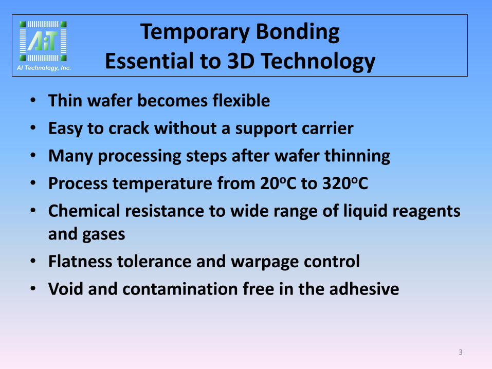
Temporary Bonding Essential to 3D Technology
• Thin wafer becomes flexible
• Easy to crack without a support carrier
• Many processing steps after wafer thinning
• Process temperature from 20oC to 320oC
• Chemical resistance to wide range of liquid reagents and gases
• Flatness tolerance and warpage control
• Void and contamination free in the adhesive
3

Thin Wafer Processing
4Source: ITRI

3D Wafer Level and TSV Processing Needs New Specialty Temporary Bonding Adhesives
5

Temporary Bonding DebondingAdhesive
Ideally one TBDB adhesive to satisfy all processing• Low to high temperature• Resistance to all types of chemicals• Physical mechanical properties
In practice choice of different TBDB depends on • Wafer materials and types• Device types and sensitivity• Support carrier types• Bonding conditions• Process conditions• Debonding conditions• Residues and cleaning issues
6

Temporary Bonding DebondingAdhesive Types by Temperature
Processing temperature ranges
• 20 – 120oC for singulation or back-grinding of fabricated wafers, thin films, ceramics, sensors, lenses, solar cells
• 120 – 180oC for thermoset curing, sputtering
• 180 – 260oC for TSV, etching, bumping, reflow
• 260 – 320oC for plasma, sputtering, metallization
7

Temporary Bonding DebondingAdhesives by Materials Classification
Bonding materials may include
• Low temperature waxes
• Hydrocarbon oligomers and polymers
• Acrylates modified
• Epoxy modified
• Silicones modified
• High temperature thermoplastics
8

Temporary Bonding DebondingAdhesives by Debonding Mechanism
Debonding methods
• Mechanical separation
• UV curing and release
• Heat curing and release
• Thermal sliding
• Chemical activation or solvent swelling
• Laser activation
9
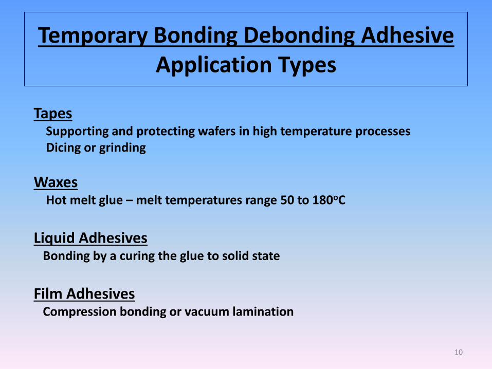
Temporary Bonding Debonding Adhesive Application Types
Tapes Supporting and protecting wafers in high temperature processes Dicing or grinding
Waxes Hot melt glue – melt temperatures range 50 to 180oC
Liquid AdhesivesBonding by a curing the glue to solid state
Film Adhesives Compression bonding or vacuum lamination
10

High Temperature Temporary Bonding Adhesive Tape
• High temperature adhesive supported on high temperature polymer film such as PET, PI, PS, LCP
• High temperature from 150 - 250oC
• CTE and shrinkage consideration
• Cooling down allowing cohesion to minimize residues
• High bond strength but lower modulus
• Double sided sheet available for bonding to carrier
11

Temporary Bonding Debonding AdhesiveIPA Soluble Wax Liquid or Film
• Low viscosity solution in isopropyl alcohol
• Spin coating up to 3000 rpm to get thin coating of rigid non-tacky adhesive layer onto a wafer carrier
• Bonding to a wafer at 85oC
• Over 1000 psi adhesion strength
• Heat slide off at 120 – 130oC
• Rinsing with IPA to remove all residues
• Varieties of IPA-soluble wax to cover temperature ranges from 60oC to 160oC
• Also available as wax-film which can be laminated on to a wafer carrier at 85oC and then bonding to wafer
12

High Temperature Temporary Bonding Hydrocarbon Base Adhesive
• Hydrocarbon base adhesive modified to give adhesion and thermal stability at 150 – 250oC
• Excellent resistance to acids, bases, and polar solvents
• Adhesive in liquid form dissolved in hydrocarbon fluid can be spin coated into thin layer on wafer carrier
• Adhesive in film format can be laminated at 150oC as thin film on wafer carrier
• Adhesive film protected by release liner on both side
• Relatively low bond strength
• Dismount by heat sliding or using non-polar solvents such as naphtha and mineral spirit.
13
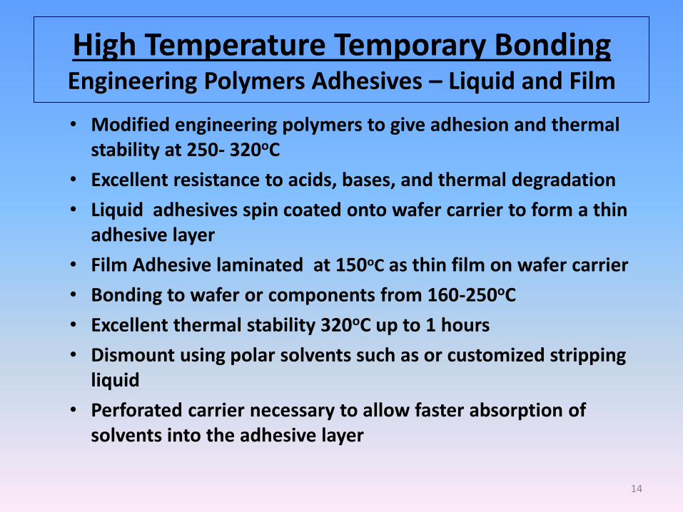
High Temperature Temporary Bonding Engineering Polymers Adhesives – Liquid and Film
• Modified engineering polymers to give adhesion and thermal stability at 250- 320oC
• Excellent resistance to acids, bases, and thermal degradation
• Liquid adhesives spin coated onto wafer carrier to form a thin adhesive layer
• Film Adhesive laminated at 150oC as thin film on wafer carrier
• Bonding to wafer or components from 160-250oC
• Excellent thermal stability 320oC up to 1 hours
• Dismount using polar solvents such as or customized stripping liquid
• Perforated carrier necessary to allow faster absorption of solvents into the adhesive layer
14
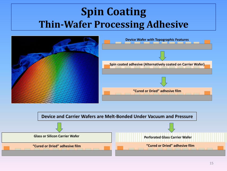
Spin Coating Thin-Wafer Processing Adhesive
15
“Cured or Dried” adhesive film
Glass or Silicon Carrier Wafer Perforated Glass Carrier Wafer
“Cured or Dried” adhesive film
Device and Carrier Wafers are Melt-Bonded Under Vacuum and Pressure
Spin coated adhesive (Alternatively coated on Carrier Wafer)
“Cured or Dried” adhesive film
Device Wafer with Topographic Features

Film Adhesive Simplified Application of Temporary Bonding Adhesive
16

3D Wafer Level and TSV Processing Productivity will be Dramatically Improved with a Properly Engineered
Temporary Bonding Film Instead of Spin Coating Adhesive
17
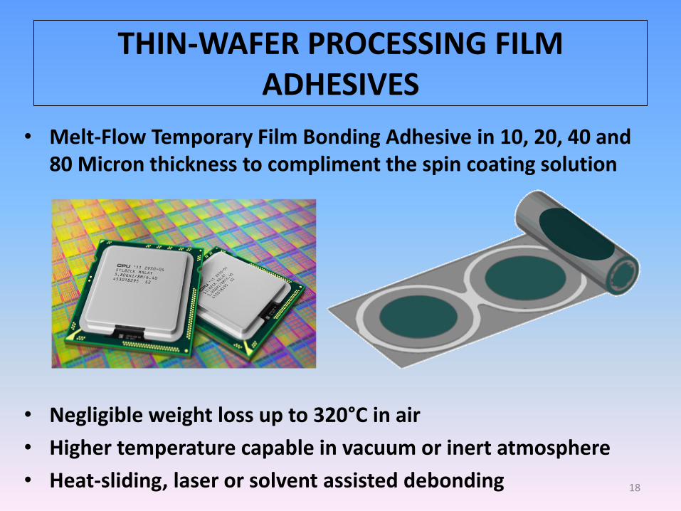
THIN-WAFER PROCESSING FILM ADHESIVES
• Melt-Flow Temporary Film Bonding Adhesive in 10, 20, 40 and 80 Micron thickness to compliment the spin coating solution
• Negligible weight loss up to 320°C in air
• Higher temperature capable in vacuum or inert atmosphere
• Heat-sliding, laser or solvent assisted debonding 18
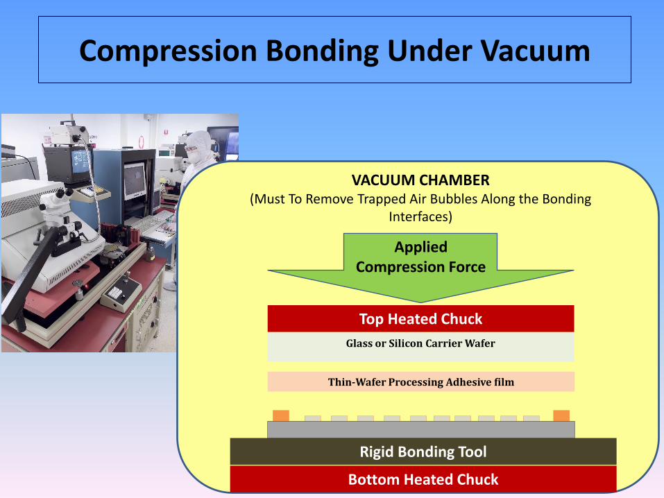
Compression Bonding Under Vacuum
19
Thin-Wafer Processing Adhesive film
Glass or Silicon Carrier Wafer
Top Heated Chuck
Applied Compression Force
Rigid Bonding Tool
Bottom Heated Chuck
VACUUM CHAMBER (Must To Remove Trapped Air Bubbles Along the Bonding
Interfaces)

Thin-Wafer Processing Film Adhesive Enables Options Not Possible with Spin Coating Adhesive
20AIT Thin Wafer Processing Adhesive film
Glass or Silicon Carrier Wafer Perforated Glass Carrier Wafer
AIT Thin Wafer Processing Adhesive Film
Device and Carrier Wafers are Melt-Bonded Under Vacuum and Pressure
Device Wafer with Topographic Features
Place AIT Film Adhesive Between Device and Carrier Wafer
Thin-Wafer Adhesive Films are available up to 80
or more micron while spin coating may need multiple
coatings on both the carrier and device wafer to
achieve the same for high
topographic wafer

Use of Wafer Processing Film Adhesive More Compatible with Clean Room Operations
21

Stresses within Temporary Wafer Processing Must be Minimized with Stress Absorbing Adhesive
3-D Model (Suhir)
1-D Model (AIT, 1986)
Device Wafer
Silicon or Glass Carrier Wafer
WPA
ε
ε
22

It is critical and necessary criterion
that wafer processing are
performed with void-free bonded device and carrier
wafers.
Voids in the bond-line can lead to
defects including poor grind finish, poor uniformity,
stress to thinning wafer during high-vacuum processes,
and others.
23
C-SAM IMAGING OF BONDED PAIR OF
DEVICE AND CARRIER WAFERS IS THE IDEAL METHOD
IN ENSURING COMPLETE VOID-
FREE BONDING

Thin-Wafer Processing Adhesive Maintain Bonding Integrity When Exposed
to Acid, Solvent and Vacuum Exposures
24
Lithography + CVD Oxide Dry Etch + Resist Removal:• Solvent resistance• Plasma resistance• Stripper resistance
Thin-Wafer Processing Adhesive film
Glass or Silicon Carrier Wafer
Thin-Wafer Processing Adhesive film
Glass or Silicon Carrier Wafer
Sputtering + Lithography + Electro-Plating + Resist Removal :• Non-Outgassing in
vacuum• Acid resistance• Stripper resistance
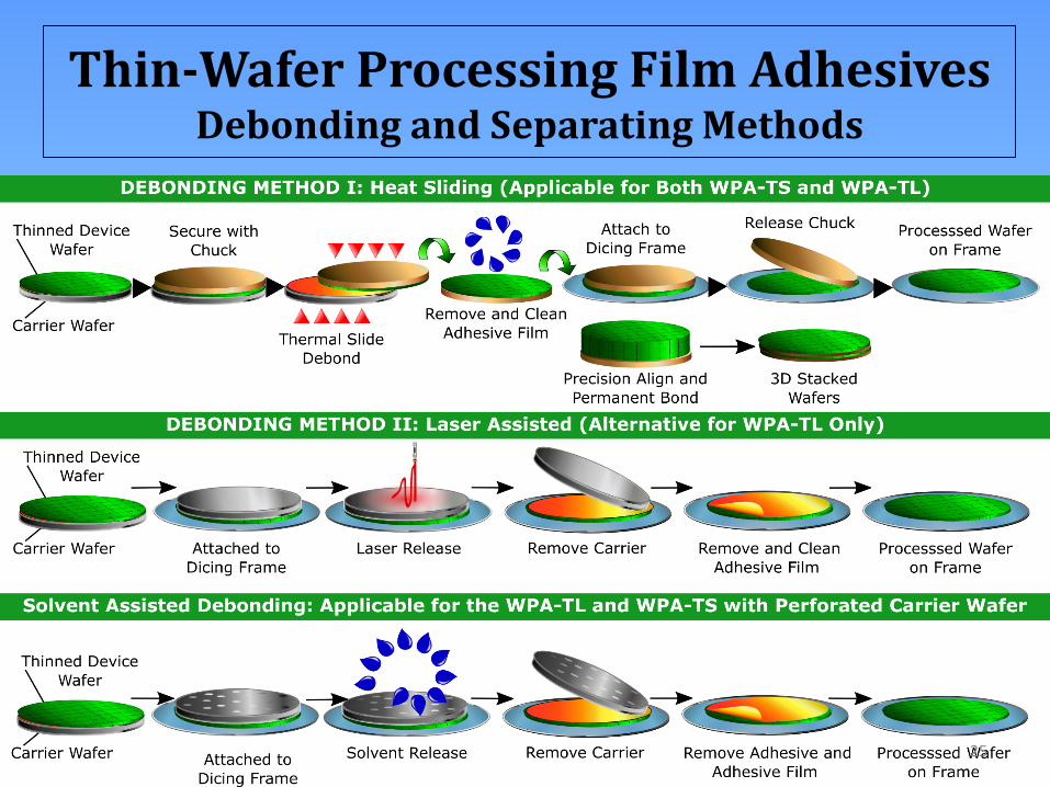
Thin-Wafer Processing Film Adhesives Debonding and Separating Methods
25

Heat-Sliding Separation-Debondingat 250-300°C with Shear Forces
26
Thin-Wafer Processing Adhesive film
Thin -Wafer Processing Adhesive film
Glass or Silicon Carrier Wafer
Top Heated ChuckApplied Shear Force
Rigid Bonding Tool
Bottom Heated Chuck
Applied Shear Force

Thin-Wafer Processing Film Adhesive Ablated by Laser to Allow Ease of Debonding
Separation Between Device and Carrier Wafer
AIT Thin Wafer Processing Adhesive film
Glass or Silicon Carrier Wafer
Tuned Laser Programmed to Pass Through the Glass Carrier and Focused Energy to Heat Up the AIT WPA-TL-330 Layer Below the Carrier Wafer to Locally Decompose a Thin Layer of Adhesive for Debonding-Separation
AIT Thin Wafer Processing Adhesive film
Glass or Silicon Carrier Wafer
27
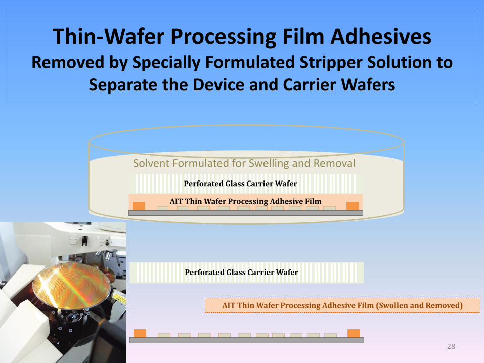
Perforated Glass Carrier Wafer
AIT Thin Wafer Processing Adhesive Film (Swollen and Removed)
Perforated Glass Carrier Wafer
AIT Thin Wafer Processing Adhesive Film
Solvent Formulated for Swelling and Removal
Thin-Wafer Processing Film Adhesives Removed by Specially Formulated Stripper Solution to
Separate the Device and Carrier Wafers
28
Temporary Bonding Debonding AdhesiveSummary Remarks
A diversified portfolio of materials for temporary bonding allows for many different innovative approaches insolvingthe thin wafer processing issues in many different types of processing
Debonding after high temperature processing remains challenging in many applications
Open-minded collaboration among the user, equipment manufacturers, and material suppliers is important for future advance.
29

THANK YOU!AI Technology, Inc. (AIT)www.aitechnology.com
Company History
• AI Technology, Inc. headquarters is located in the company owned complex in Princeton Junction, New Jersey with close to 52,000 square feet office and manufacturing facilities within a 16 acre site. In addition to the New Jersey headquarters, the company has offices in Hong Kong and Shenzhen China. AIT has approximately 80 employees world-wide.
• AIT is an ISO 9001:2000 quality management certified manufacturing company.
1. Pioneered the use of flexible, stress adhesive films and pastes used in most advanced commercial and military applications since 1985
2. More than 30 US patents in materials for electronics and microelectronics manufacturing
3. First phase-change thermal adhesives and pads, patented compressible phase-change thermal interface pads, lowest thermal interface resistance greases and gels, compressible and conformable thermal gap-pads
4. Advanced DDAF: 3 micron thickness for up to 450mm wafer
5. Patent-pending thermally conductive solar back-sheets
6. Insulated metal thermal substrate with 2xtimes thermal conductivity for metal-core printed wiring boards
7. First thin wafer processing temporary bonding film adhesive
Pioneering and Innovative Products and Materials Technologies for Highest Performance and Reliability
Corporate Headquarters in Princeton, New Jersey
30

16 Acres of Manufacturing
and Development Center
in Princeton Junction, NJ
One of the most
comprehensive lines of
microelectronic
packaging and wafer
processing materials 31