terahertz waveguides with low transmission losses...
TRANSCRIPT

Terahertz waveguides with low transmission losses: characterization and applications
Oleg Mitrofanov *a, Miguel Navarro-Cia a,b, Miriam S. Vitiello c, Jeffrey E. Melzer d and James A. Harrington d
aDepartment of Electronic and Electrical Engineering, University College London, London WC1E 7JE, UK
bDepartment of Electrical and Electronic Engineering, Imperial College London, London SW7 2BT, UK
cNEST, CNR—Istituto Nanoscienze and Scuola Normale Superiore, Pisa, Italy dSchool of Engineering, Rutgers University, Piscataway, New Jersey 08854 USA
ABSTRACT
Research in the area of terahertz (THz) waveguides has seen a rapid progress recently and has led to demonstration of THz waveguides with transmission losses comparable to losses in air. We will discuss dielectric-lined hollow metallic waveguides, in which THz waves propagate with attenuation as low as 1 dB/m and dispersion of 6 ps/(THz·m), and compare them to other low-loss THz waveguides. As a key technique for THz waveguide research, we will discuss the application of THz near-field microscopy in combination with THz time-domain spectroscopy for waveguide characterization. This technique allows us to map spatial profiles of normal modes and to measure transmission loss and dispersion spectra for individual modes within the THz range.
Keywords: Terahertz, hollow metallic waveguides, terahertz spectroscopy, near-field imaging, waveguide modes, dispersion, transmission loss, mode interference.
1. INTRODUCTION A number of applications, such as gas spectroscopy, endoscopy, and signal transmission, can be realized and/or simplified by utilizing guided terahertz (THz) wave propagation. THz waveguides can also help solving some technological challenges, for example, integration of THz quantum cascade lasers (QCL) into THz systems through shaping THz beams emitted from QCLs. During the last few years, intensive research on THz waveguides has demonstrated several waveguide concepts and realized relatively low transmission losses (~1 dB/m),1,2 comparable to the level of absorption in air. Waveguides with low dispersion, in addition to the low signal attenuation, are particular interesting as they can enable the use of guided THz waves in time-domain spectroscopy and imaging systems.3 Within the wide spectrum of THz waveguides investigated to date, the group of low-loss THz waveguides shares common features.1,2,4-8 A large hollow (or porous) core is typically used for guiding as THz waves propagating in air suffer smaller attenuation than waves propagating in dielectrics. The core can be filled with either dry air or nitrogen gas to eliminate absorption due to water vapor. A large core diameter is commonly used to reduce the losses due to absorption in the waveguide walls.9 Transmission losses in hollow waveguides typically exhibit a strong dependence on the core size. For example, Ohmic losses is hollow cylindrical metallic waveguides are inversely proportional to the third power of the core radius. The dominant mode profile and size are similar in many low-loss waveguides. As a result, their characterization and integration into THz systems face similar challenges. *[email protected]
Invited Paper
Terahertz Emitters, Receivers, and Applications V, edited by Manijeh Razeghi, Alexei N. Baranov,John M. Zavada, Dimitris Pavlidis, Proc. of SPIE Vol. 9199, 91990I · © 2014 SPIE
CCC code: 0277-786X/14/$18 · doi: 10.1117/12.2062758
Proc. of SPIE Vol. 9199 91990I-1
Downloaded From: http://proceedings.spiedigitallibrary.org/ on 06/17/2015 Terms of Use: http://spiedl.org/terms

Dielectric-lined hollow cylindrical metallic waveguides are among the THz waveguides with the lowest losses demonstrated to date.1,2,9 This waveguide is a modified version of the hollow metallic waveguide, where the inner walls are lined with a thin layer of dielectric.10,11 The inner wall modification has a significant impact on the waveguide characteristics: the transmission loss can be reduced from about 3-5 dB/m in the metallic waveguides to the level below 1 dB/m for the same waveguide size.12,13 This effect is due to a change in the energy distribution for the dominant waveguide mode.9 Compared to the metallic waveguides the energy density is reduced near the waveguides walls. Dispersion in the dielectric-lined hollow waveguides remains relatively small, similar to the hollow metallic waveguides.14 Although we will focus on this type of THz waveguides, the characterization methods and integration aspects discussed below apply to a wider range of THz low-loss waveguides.
2. LOW-LOSS TERAHERTZ WAVEGUIDES 2.1 Transmission losses in THz waveguides
Transmission losses in THz waveguides arise mainly from material absorption. Leakage of the transmitted energy outside of the waveguide volume can be significant in some of the proposed THz waveguides, e.g. in dielectric tube waveguides7 and parallel-plate waveguides.15,16 However in waveguides with complete mode confinement the radiation leakage is avoided, and the material absorption at THz frequencies, which includes Ohmic losses in metallic surfaces and absorption inside dielectrics, remains the main loss mechanism. To minimize the impact of material losses, the general approach of transmitting the energy in a hollow region of the waveguide has been implemented in all low-loss THz waveguides so far.9,17 Closed hollow regions can be filled with nitrogen gas or dry air to eliminate absorption due to water vapor. Waveguide designs following this approach can be divided into three categories: hollow metallic waveguides (including waveguides with dielectric-lined or corrugated walls); photonic crystal waveguides (including pipe waveguides); and porous dielectric waveguides. Reported losses and dispersion for waveguides in these categories can be found in recent review articles.9,17 Transmission losses and dispersion decrease substantially as the area of the hollow region increases. However practical applications of large area waveguides present two major difficulties: waveguide flexibility reduces and the number of supported modes increases. 2.2 Dielectric-lined hollow cylindrical waveguides
The dielectric-lined hollow cylindrical metallic waveguide is a modified hollow metallic waveguide, where the inner metallic surface is coated with a thin dielectric layer, typically 10–50 μm for THz waveguides (Fig. 1(a)). The modified walls change profiles of supported modes. A hybrid HE11 mode, with the transmitted energy concentrated near the waveguide center, is formed in the dielectric-lined waveguide.8 This mode was demonstrated to have attenuation as low as 1 dB/m for a 2.2 mm diameter waveguide,1 and dispersion as low as 6 ps/THz/m at ~2 THz.11 A detailed overview of dielectric-lined waveguides for THz applications the can be found in Ref. 7. Here we summarize their properties. Dispersion and attenuation properties of a dielectric-lined waveguide critically depend on the dielectric layer thickness and the waveguide diameter.7,8,10,11 The dielectric layer creates a wide transmission band for the hybrid HE11 mode. The spectral position of the band is determined by the thickness and the refractive index of the dielectric. A 10 μm thick layer made of common polymers with a refractive index of ~1.5, for example, produces a transmission band centered at 3-4 THz. A thicker layer shifts the transmission band to the lower frequencies. Two approaches have been demonstrated for fabrication of THz dielectric-lined waveguides. The waveguide structure can be made by coating of inner metallic walls with dielectrics and by deposition of metallic films over plastic tubes.1,2,18 Good quality waveguides for the high-frequency THz range (2-5 THz) have been fabricated using the first approach. Fig. 1(b-d) shows examples of waveguides made by coating the inner surface of glass tubing with a 1 μm thick layer of silver and a ~10-14 μm thick layer of polystyrene (PS). This process allows producing waveguides for the region of ~2-3 THz and above. The same process in principle can be applied for waveguides with the transmission band at 1-2 THz if 20-30 μm thick uniform PS films can be deposited. Flexible waveguides can be realized using small diameter (~1 mm) glass tubes.19 The small diameter permits bending this waveguide to a radius of 10-15cm (Fig. 1(d)). The glass tubing however becomes rigid for larger bore diameters required for lower frequencies.
Proc. of SPIE Vol. 9199 91990I-2
Downloaded From: http://proceedings.spiedigitallibrary.org/ on 06/17/2015 Terms of Use: http://spiedl.org/terms

Dielectric-10 5 Van
Ag - 1 linCored =1 -4 mm
Figure 1. (a) Schematic diagram of the inner wall of the dielectric-lined hollow metallic waveguides with typical dimensions for reducing transmission losses at 0.2-5.0 THz. Photographs of dielectric-lined hollow THz waveguides made using glass tubing: (a) cleaved facet of a 1.6 mm diameter waveguide and (b) examples of waveguides with the inner bore diameter ranging from 1.0 mm to 2.2 mm. (d) Bending of a 1mm diameter waveguide made using standard glass tubing.
In the second (reversed) approach, a metallic layer is deposited over a thin-wall plastic tube.2,18 As the wall thickness in available plastic tubes is typically 40-120 μm thick, this approach can produce waveguides only for the low frequency band (0.5-1.5 THz). We fabricated THz waveguides using commercially available Teflon and polyamide tubing. Transmission losses in these waveguides however were found to be larger than in metallic waveguides of similar diameter.
2.3 Application of THz time-domain spectroscopy and imaging for waveguide characterization
In this section we discuss the application of THz time-domain spectroscopy (THz-TDS) for characterization of transmission losses and dispersion. In the THz-TDS method, a THz pulse is sent through the waveguide, and the transmission loss and dispersion characteristics are determined directly from the Fourier spectra of the pulses before and after transmission through the waveguide.20 There are however two difficulties with applying the standard THz-TDS approach. First of all, the large core size in low-loss waveguides generally allows multiple modes of wave propagation. The THz pulse therefore can travel through a multimode waveguide as a superposition of several modes. The Fourier spectra as a result can be affected by interference of these modes and show regular interference peaks.20 Secondly, the coupling coefficient for a THz beam focused on a waveguide (using lenses or parabolic mirrors) varies with frequency. The frequency dependent coupling coefficient therefore may effectively ‘suppress’ or ‘enhance’ losses in a wide band of frequencies. To mitigate these problems, we developed a near-field THz time-domain spectroscopy characterization system utilizing the cut-back loss measurement methodology, commonly used for testing optical waveguides, and near-field spatial mapping. The system diagram is shown in Fig. 2(a). A 1 mm thick ZnTe crystal is used for generation of broadband THz pulses through the process of optical rectification of 100 fs pulses from a Ti:Sapphire mode-locked laser. The generated THz beam is incident on the first THz waveguide after passing though a silicon filter, which blocks the infrared beam. The waveguide input is positioned at a distance of 0.5-2 mm away from the filter. After travelling through the first waveguide, the THz pulse is detected at the waveguide output (within ~0.1-0.2 mm) by a photoconductive antenna behind a metallic screen with a sub-wavelength size aperture.18 The small aperture (typically 10 μm) allows us to map
Proc. of SPIE Vol. 9199 91990I-3
Downloaded From: http://proceedings.spiedigitallibrary.org/ on 06/17/2015 Terms of Use: http://spiedl.org/terms
x(D)
(Ag /RS:149mm
0 5 10 15time (pa) (c)
(a)
excitationpulse 1
ZnTe Si filter
/ wg1gate
detector
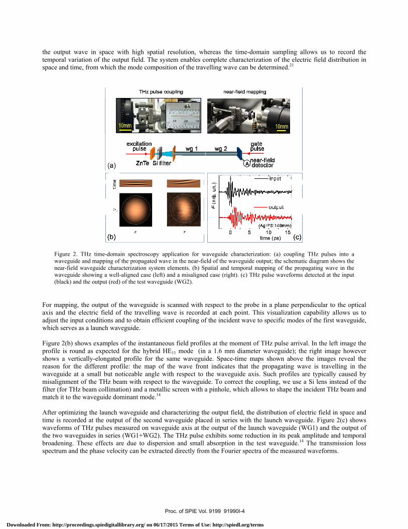
the output wave in space with high spatial resolution, whereas the time-domain sampling allows us to record the temporal variation of the output field. The system enables complete characterization of the electric field distribution in space and time, from which the mode composition of the travelling wave can be determined.21
Figure 2. THz time-domain spectroscopy application for waveguide characterization: (a) coupling THz pulses into a waveguide and mapping of the propagated wave in the near-field of the waveguide output; the schematic diagram shows the near-field waveguide characterization system elements. (b) Spatial and temporal mapping of the propagating wave in the waveguide showing a well-aligned case (left) and a misaligned case (right). (c) THz pulse waveforms detected at the input (black) and the output (red) of the test waveguide (WG2).
For mapping, the output of the waveguide is scanned with respect to the probe in a plane perpendicular to the optical axis and the electric field of the travelling wave is recorded at each point. This visualization capability allows us to adjust the input conditions and to obtain efficient coupling of the incident wave to specific modes of the first waveguide, which serves as a launch waveguide. Figure 2(b) shows examples of the instantaneous field profiles at the moment of THz pulse arrival. In the left image the profile is round as expected for the hybrid HE11 mode (in a 1.6 mm diameter waveguide); the right image however shows a vertically-elongated profile for the same waveguide. Space-time maps shown above the images reveal the reason for the different profile: the map of the wave front indicates that the propagating wave is travelling in the waveguide at a small but noticeable angle with respect to the waveguide axis. Such profiles are typically caused by misalignment of the THz beam with respect to the waveguide. To correct the coupling, we use a Si lens instead of the filter (for THz beam collimation) and a metallic screen with a pinhole, which allows to shape the incident THz beam and match it to the waveguide dominant mode.14 After optimizing the launch waveguide and characterizing the output field, the distribution of electric field in space and time is recorded at the output of the second waveguide placed in series with the launch waveguide. Figure 2(c) shows waveforms of THz pulses measured on waveguide axis at the output of the launch waveguide (WG1) and the output of the two waveguides in series (WG1+WG2). The THz pulse exhibits some reduction in its peak amplitude and temporal broadening. These effects are due to dispersion and small absorption in the test waveguide.14 The transmission loss spectrum and the phase velocity can be extracted directly from the Fourier spectra of the measured waveforms.
Proc. of SPIE Vol. 9199 91990I-4
Downloaded From: http://proceedings.spiedigitallibrary.org/ on 06/17/2015 Terms of Use: http://spiedl.org/terms

20
-0 40
o 60 -
80 -
05 10 1.5
r QdL
exp: TDSmodel.: a=aAg:
- --- tan 8=0.005----tan 8=0.023-
model.: a=0.32aAg:
- - - tan 80.010-2.0 2.5 30
1
IC
-40 (dB) O
0
E311 20
T:s
8 40
801 2 4 5
2.4 Waveguide transmission properties of dielectric-lined hollow metallic waveguides
Low-loss transmission in the dielectric-lined hollow cylindrical metallic waveguides occurs in the first transmission band as the hybrid HE11 mode. Transmission spectra for a 1 mm bore diameter waveguide with a PS layer deposited on silver (Ag) walls are illustrated in Fig. 3. Simulated spectra are plotted in Fig. 3(a) for the PS layer thickness 8, 10 and 14 μm and for nominal and increased losses in the Ag and PS layers. All spectra show the transmission band and two absorption bands with their positions defined by the thickness of the PS layer.
Figure 3. Transmission properties of the HE11 mode in the 1mm diameter PS-lined hollow cylindrical waveguide. (a) Simulated transmission loss spectra of the Ag/PS waveguide with PS thickness: 8 μm (red), 10 μm (blue) and 14 μm (green) for several case of ohmic and dielectric losses. (b) The transmission spectrum measured by the near-field THz-TDS system (red line); the diamond marks the experimentally measured transmission loss of ~4.2 dB/m using a single frequency (2.85THz) QCL and the cutback method. (c) A near-field map of the waveguide mode at ~2 THz (adapted from Ref. 19)
In the center of the transmission band (at ~2.5 THz), the transmission loss is at a level of 4-5 dB/m. In the first absorption band (from ~1 to 1.5 THz), the loss can increase to 70–80 dB/m depending on losses in PS and Ag. Measurements of waveguides with such a variation of transmission properties are susceptible to experimental errors. The low level of absorption in the transmission band ideally requires a long sample, whereas the small amount of output power within the absorption band requires a short sample. The length of the test waveguide sample therefore is chosen to yield measurable loss levels within both the transmission and absorption regions. The experimental results for a test sample of 220 mm long are shown in Fig. 3(b). The spectrum clearly shows the absorption and the transmission bands, consistent with the simulations. To confirm the results of the THz-TDS measurements in the transmission band, the plot also shows the loss value of 4.2 dB/m measured using a THz QCL operating at 2.85THz and the cut-back method.19 The HE11 mode profile at the frequency of ~2 THz shown in Fig. 3(c) also agrees with the simulations (Fig. 3(a)). In the absorption band, however, the measured loss is significantly higher than that predicted by numerical studies. Within the absorption band, the propagating wave carries a significant amount of energy near the walls. It suggests that the impact of the metallic and dielectric layers on the waveguide performance is important. The difficulty of explaining the experimental data with standard numerical models of surface conductivity and surface roughness suggests that it needs to be addressed more rigorously.
Proc. of SPIE Vol. 9199 91990I-5
Downloaded From: http://proceedings.spiedigitallibrary.org/ on 06/17/2015 Terms of Use: http://spiedl.org/terms

Phase velocity
(v/c)
The THz-TDS method also allows us to obtain dispersion characteristics. Figure 4 shows examples of experimental phase velocity plots for the 1.8mm diameter metallic and dielectric-lined metallic waveguides. The measurements agree very well with precise analytical solutions for the TE11 and TE01 modes, showing the accuracy of the characterization method. We note that for the TE01 mode characterization, the near-field probe is positioned at the electric field maximum, displaced from the waveguide axis (inset). For the HE11 mode, which does not have an analytical solution, the dispersion relationship still can be approximated by an analytical model within the transmission band.
Figure 4. Phase velocity plots for the TE11 mode in the metallic (Ag) waveguide (black), and HE11 (red) and TE01 modes in the dielectric-coated (Ag/PS) waveguide: symbols show the experimental data measured in the far-field and near-field zones respectively; solid lines show the exact analytical solutions for the TE11 and TE01 modes in the metallic waveguide and an analytical approximation for the HE11 mode; insets: mode profiles for the TE11, HE11 and TE01 modes with measurement locations marked by crosses (adapted from Ref. 14).
The group-velocity dispersion for the HE11 and TE01 modes in the dielectric-lined waveguide is relatively small because the waves travel mostly outside the dielectric in contrast to the surface wave modes on dielectric-coated metal wires and plates. The waveguide dispersion parameter D was estimated to be 0.08 ps/(μm·m) or 6 ps/(THz·m) for the HE11 mode at 2.3 THz.14 This figure corresponds to a broadening of ~1 ps for a THz pulse with the bandwidth of 80 μm after propagation through a 0.15 m long waveguide.
3. CONCLUSIONS Experimental studies and numerical calculations show that the dielectric-lined hollow metallic waveguides provide some of the best transmission characteristics among THz waveguides within a relatively large band of frequencies. In 2.2-mm diameter waveguides, the loss can be below 1 dB/m, and in 1-mm diameter flexible guides, it increases only up to ~4-5 dB/m. These waveguides can enable large-bandwidth signal transmission over distances of several meters in the spectral range of THz QCLs (2-4 THz). The combination of low loss and relatively low dispersion differentiates these waveguides from other low-loss waveguides. It allows using the waveguides not only for transmission of narrow band signals but also for transmission of THz pulses. Most low-loss THz waveguides support several modes of wave propagation. In order to integrate such waveguides in THz systems, efficient coupling to selected modes is required. The low-loss HE11 mode in the dielectric-lined hollow cylindrical waveguides is convenient for coupling to free space beams: it is linearly polarized with a Gaussian-like profile over a wide band of frequencies [Fig. 3(a)]. Estimated coupling to free space beams is over >90%. As discussed in Section 2.3, point-like THz sources can be efficiently coupled to the HE11 mode using lenses and pinholes. These waveguide can provide a solution for beam shaping of high-performance THz QCLs, which produce highly divergent far-field beam profiles. 1-mm diameter waveguides, which are suited well for the spectral range of THz QCLs, are
Proc. of SPIE Vol. 9199 91990I-6
Downloaded From: http://proceedings.spiedigitallibrary.org/ on 06/17/2015 Terms of Use: http://spiedl.org/terms

flexible enough to bend with a radius of curvature of 100-150 mm. These waveguides can be also integrated into THz spectroscopy and imaging systems. Experimental characterization is a central question for future development of low-loss THz waveguides, where advances in fabrication methods and the use of dielectrics with low absorption can make further improvements. Visualization of propagating modes is particular important for coupling into multimode waveguides, and precise characterization of transmission losses is essential for verifying numerically computed losses.
ACKNOWLEDGEMENTS This work was supported by the Engineering and Physical Sciences Research Council (grant numbers EP/G033870/1 and EP/J017671/1), the Royal Society (grant number UF080745), Imperial College through a Junior Research Fellowship (M.N.-C.), the Italian Ministry of Education, University, and Research through the program “FIRB-Futuro in Ricerca 2010” RBFR10LULP “Fundamental research on terahertz photonic devices” (M.S.V.).
REFERENCES [1] Bowden, B., Harrington, J. A., and Mitrofanov, O., “Silver/polystyrene-coated hollow glass waveguides for the
transmission of terahertz radiation,” Opt. Lett. 32(20), 2945 - 2947 (2007). [2] Matsuura, Y., Takeda, E., “Hollow optical fibers loaded with an inner dielectric film for terahertz broadband
spectroscopy,” J. Opt. Soc. Am. B 25(12), 1949-1954 (2008). [3] Mueckstein, R., Mitrofanov, O., “Imaging of terahertz surface plasmon waves excited on a gold surface by a
focused beam,” Opt. Express 19(4), 3212-3217 (2011). [4] Atakaramians, S., Afshar V, S., Fischer, B.M., Abbott, D., and Monro, T.M., “Porous fibers: a novel approach to
low loss THz waveguides,” Opt. Express 16, 376-379 (2008). [5] Hassani, A., Dupuis, A., and Skorobogatiy, M., “Porous polymer fibers for low-loss Terahertz guiding,” Opt.
Express 16, 6340-6351 (2008) [6] Lu, J. Y., Yu, C. P., Chang, H. C., Chen, H. W., Li, Y. T., Pan, C. L., Sun, C. K., “Terahertz air-core microstructure
fiber,” Appl. Phys. Lett. 92(6), 064105 (2008). [7] Chen, D., and Chen, H., “A novel low-loss Terahertz waveguide: Polymer tube,” Opt. Express 18, 3762-3767
(2010). [8] Nielsen, K., Rasmussen, H. K., Adam, A. J., Planken, P. C., Bang, O., and Jepsen, P.U., “Bendable, low-loss Topas
fibers for the terahertz frequency range,” Opt. Express 17, 8592-8601 (2009). [9] Mitrofanov, O., James, R., Fernández, F. A., Mavrogordatos, T. K., and Harrington, J. A., “Reducing transmission
losses in hollow THz waveguides,” IEEE Trans. THz Sci. Tech. 1, 124-132 (2011). [10] Carlin, J.W., and D’Agostino, P., “Normal Modes in Overmoded Dielectric-Lined Circular Waveguide”, J. Bell
Syst. Tech. 52, 453-486 (1973). [11] Miyagi, M., and Kawakami, S., “Design theory of dielectric-coated circular metallic waveguides for infrared
transmission,” J. Lightwave Technol. 2, 116-126 (1984). [12] Bowden, B., Harrington, J. A., and Mitrofanov, O., “Low-loss modes in hollow metallic terahertz waveguides with
dielectric coatings,” Appl. Phys. Lett. 93(18), 181104, (2008). [13] Tang, X.-L., Shi, Y.-W., Matsuura, Y., Iwai, K., and Miyagi, M., “Transmission characteristics of terahertz hollow
fiber with an absorptive dielectric inner-coating film,” Opt. Lett. 34(14), 2231–2233 (2009). [14] Mitrofanov, O., Harrington, J.A., “Dielectric-lined cylindrical metallic THz waveguides: mode structure and
dispersion. Optics Express,” 18(3), 1898-1903 (2010). [15] Mendis R. and Mittleman, D. M., “An investigation of the lowest-order transverse-electric (TE1) mode of the
parallel-plate waveguide for THz pulse propagation,” J. Opt. Soc. Am. B 26, 6-13 (2009) [16] Mueckstein, R, Navarro-Cía, M, Mitrofanov, O., “Mode interference and radiation leakage in a tapered parallel plate
waveguide for terahertz waves,” Appl. Phys. Lett. 102(14), 141103 (2013). [17] Atakaramians, S., Afshar V., S., Monro, T., and Abbott, D., "Terahertz dielectric waveguides," Adv. Opt. Photon. 5,
169-215 (2013). [18] Melzer, J. E., Navarro-Cía, M., Mitrofanov, O., and Harrington, J. A., "Silver-coated Teflon hollow waveguides for
the delivery of terahertz radiation," Proc. SPIE 8938, (2014).
Proc. of SPIE Vol. 9199 91990I-7
Downloaded From: http://proceedings.spiedigitallibrary.org/ on 06/17/2015 Terms of Use: http://spiedl.org/terms

[19] Navarro-Cía, M., Vitiello, M.S., Bledt, C. M., Melzer, J. E., Harrington, J.A., and Mitrofanov, O., “Terahertz wave transmission in flexible polystyrene-lined hollow metallic waveguides for the 2.5-5 THz band,” Opt. Express 21(20), 23748-23755 (2013).
[20] Gallot, G., Jamison, S. P., McGowan, R. W., and Grischkowsky, D., “Terahertz waveguides,” J. Opt. Soc. Am. B 17, 851–863 (2000).
[21] Mitrofanov, O., Tan, T., Mark, P. R., Bowden, B, and Harrington, J. A., “Waveguide mode imaging and dispersion analysis with terahertz near-field microscopy,” Appl. Phys. Lett. 94(17), 171104 (2009).
Proc. of SPIE Vol. 9199 91990I-8
Downloaded From: http://proceedings.spiedigitallibrary.org/ on 06/17/2015 Terms of Use: http://spiedl.org/terms