terms of use field-effect transistors built from all two...
TRANSCRIPT
ROY ET AL. VOL. 8 ’ NO. 6 ’ 6259–6264 ’ 2014
www.acsnano.org
6259
April 29, 2014
C 2014 American Chemical Society
Field-Effect Transistors Built from AllTwo-DimensionalMaterialComponentsTania Roy,†,‡,§ Mahmut Tosun,†,‡,§ Jeong Seuk Kang,†,‡,§ Angada B. Sachid,† Sujay B. Desai,†,‡,§
Mark Hettick,†,‡,§ Chenming C. Hu,† and Ali Javey†,‡,§,*
†Electrical Engineering and Computer Sciences, University of California, Berkeley, California 94720, United States, ‡Materials Sciences Division, Lawrence BerkeleyNational Laboratory, Berkeley, California 94720, United States, and §Berkeley Sensor and Actuator Center, University of California, Berkeley, California 94720,United States
Two-dimensional (2-D) material sys-tems have aroused immense interestin research due to the possibility of
obtaining thickness uniformity down to amonolayer without surface dangling bonds.Graphene (Gr), as a two-dimensional semi-metal has been studied extensively for thepurpose of analog and digital applications.However, the absence of an intrinsic band-gap in Gr overshadows its attractive proper-ties of small quantum capacitance andextremely high mobilities in scaled transis-tors.13 Transition metal dichalcogenides(TMDC), with an inherent bandgap, tunableby composition and the number of lay-ers, have ignited significant interest andpromise over the past few years for both
electronic and optoelectronic applica-tions.47 For instance, MoS2 and WSe2 havebeen used to obtain excellent switchingcurrent ratios (up to 108), and ideal sub-threshold slope (60mV/decade).812 One ofthe primary advantages of layeredmaterialsis, in principle, the absence of danglingbonds, which rules out performance degra-dation due to interface states.13 Uniquely,heterostructures using two-dimensionalmaterials would not suffer from constraintsof lattice mismatch. A layered material canbe seamlessly transferred onto another, andbond by van der Waal's (vdW) forces, leav-ing the interface pristine. An ideal transistorstructure would, therefore, be composedof a TMDC material as the channel, with a
* Address correspondence [email protected].
Received for review March 28, 2014and accepted April 29, 2014.
Published online10.1021/nn501723y
ABSTRACT
We demonstrate field-effect transistors using heterogeneously stacked two-dimensional materials for all of the components, including the semiconductor,
insulator, and metal layers. Specifically, MoS2 is used as the active channel material, hexagonal-BN as the top-gate dielectric, and graphene as the source/
drain and the top-gate contacts. This transistor exhibits n-type behavior with an ON/OFF current ratio of >106, and an electron mobility of∼33 cm2/V 3 s.
Uniquely, the mobility does not degrade at high gate voltages, presenting an important advantage over conventional Si transistors where enhanced surface
roughness scattering severely reduces carrier mobilities at high gate-fields. A WSe2MoS2 diode with graphene contacts is also demonstrated. The diode
exhibits excellent rectification behavior and a low reverse bias current, suggesting high quality interfaces between the stacked layers. In this work, all
interfaces are based on van der Waals bonding, presenting a unique device architecture where crystalline, layered materials with atomically uniform
thicknesses are stacked on demand, without the lattice parameter constraints. The results demonstrate the promise of using an all-layered material system
for future electronic applications.
KEYWORDS: layered materials . transition metal dichalcogenides . graphene . hexagonal boron nitride . MoS2 . heterolayers
ARTIC
LETerms of Use
ROY ET AL. VOL. 8 ’ NO. 6 ’ 6259–6264 ’ 2014
www.acsnano.org
6260
layered insulator as the gate dielectric, and layeredmetallic source/drain and gate contacts. Atomicallythin p-n diodes have been reported, using MoS2 andWSe2 monolayers as the electron and hole conductinglayers, respectively.1416 These vdW heterostructurediodes have exhibited excellent rectification behaviorowing to the abruptness of the 2D2D interface, withideality factor of 1.2. MoS2 transistors with graphenesource/drain contacts have been used to fabricateflexible, transparent transistors.17 Also, flexible andtransparent MoS2 transistors with graphene source/drain contacts were fabricated with h-BN as back gatedielectric, demonstrating negligible hysteresis in trans-port characteristics.18 Heterostructures with 2D mate-rials have been used for memory applications andtunnel transistors. Gr/MoS2 heterostructures havebeen used for nonvolatile memory cells.19 Tunneltransistors fabricated with Gr/hexagonal-BN (h-BN)/Grand Gr/MoS2/Gr open the prospect of obtaining steeptransistors with such an architecture.20 Vertical Gr/h-BN/Gr heterostacks have also exhibited negative dif-ferential resistance, allowing the prospect of vdWheterostructures in analog electronics.21 Gr/WS2/Grheterostructures have demonstrated strong light-matter interactions, leading to enhanced photonabsorption and electronhole creation.22 This hasopened the possibility of flexible photovoltaic deviceswith layered 2D materials. Heterobilayers of WSe2 andMoS2 have shown strong interlayer coupling withspatially direct absorption and spatially indirect emis-sion, exhibiting yet another unique property of TMDCheterostructures. TMDC heterojunctions with IIIV, Si,and carbon nanotubes have also been explored pre-viously, demonstrating electrically active vdW inter-faces built from highly dissimilar semiconductors.2326
However, a transistor made completely from two-dimensional materials to leverage the absence ofinterface states with digitally controlled and atomicallyuniform thickness has not been reported so far. In thiswork, we use large area chemical vapor deposited
(CVD) Gr to contact few-layer MoS2 crystals. We useexfoliated hexagonal boron nitride as the layeredgate dielectric and exfoliated Gr as the top-gate con-tact. The resulting field-effect transistor (FET) madecompletely of layeredmaterials exhibits a highON/OFFcurrent ratio of >106, with a MoS2 electron mobilityof 33 cm2/V 3 s. We also demonstrate the rectificationbehavior of an all-2D diode, using MoS2WSe2 het-erojunction contacted with Gr as the source/drainelectrodes.Figure 1 shows the fabrication steps and corre-
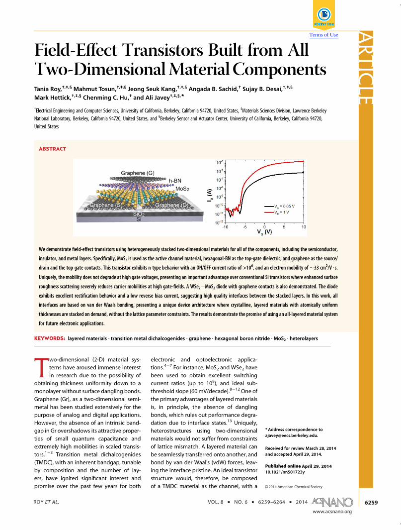
sponding optical images of a representative all-2DFET. The details of the process are as follows. CVDgrown bilayer or monolayer Gr on a Cu foil was coatedwith PMMA. The PMMA-coated substrate was treatedwith dilute HNO3 and the Cu was etched by insertingthe foil into an ammonium persulfate solution bathfor 18 h. After the Cu foil was completely etched away,the floating PMMA coated Gr was scooped out of thebath and transferred onto a Si/SiO2 (260 nm) substrate(Figure 1(i)). The sample was baked at 220 C for 5 minto improveGr adhesion on the SiO2 surface followedbyPMMA removal using acetone.27,28 Ni/Au (30 nm/30 nm) bond padswere then formed by electron-beam(e-beam) lithography, evaporation and resist lift-off. Grwas subsequently patterned using e-beam lithographyand oxygen plasma etching to define the S/D electro-des of the FET (Figure 1(ii)). MoS2, h-BN, and Gr multi-layers as the active channel, gate dielectric, and thegate electrode, respectively, were sequentially stackedon the Gr S/D contacts using a pick and transferprocess. Specifically, MoS2, h-BN and Gr multilayerswere first exfoliated onto Si/SiO2 process substrates.Flakes of interest were patterned into rectangularshapes with desired dimensions using electron-beamlithography and dry etching. MoS2 and h-BN wereetched using XeF2, and Grwas etched usingO2 plasma.The substrates were then spin coated with PMMA(6 μm in thickness). PMMA was used as a carrier layerto pick the flake of interest off the substrate, and to
Figure 1. Schematics (not to scale) of the fabrication process steps (top) and the corresponding optical microscope images(bottom) of a representative all-2D FET. (i) Transfer of large-area CVD grown bilayer graphene onto a Si/SiO2 substrate. (ii)Bilayer graphene patterning by O2 plasma to define S/D contacts. (iii) Transfer of a few-layer MoS2 flake on top of thepatterned grahene S/D contacts. (iv) Transfer of a few-layer h-BN gate dielectric, overlapping theMoS2 channel. (v) Transfer ofamultilayer graphene topgate electrode. (vi) Opticalmicroscope imageof a fully fabricated all-2D transistor. Scale bar is 5 μmfor all images.
ARTIC
LE

ROY ET AL. VOL. 8 ’ NO. 6 ’ 6259–6264 ’ 2014
www.acsnano.org
6261
dry-transfer onto the device substrate. First, using anengraver, the PMMA slab around the patterned flake ofinterest was cut under an optical microscope. The slabwas poked from all sides to release from the SiO2
substrate. The PMMA slab with the flake was thenpicked with a needle under a microscope, and trans-ferred onto the targeted area on the device substrate.The sample was subsequently annealed at 180 C for2 min after each transfer step to improve the adhesionof the transferred flakes to the substrate. The PMMAcarrier layer was removed by immersion in dichloro-methane after each transfer step. With this dry transfermethod, a MoS2 flake was transferred in between theprepatterned Gr S/D contacts (overlapping each Grcontact) to form the active channel (Figure 1(iii)). Ah-BN flake was then dry-transferred onto the MoS2channel area to form the gate dielectric (Figure 1(iv))followed by the transfer of a multilayer Gr flake to formthe top-gate contact (Figure 1(v)). The device wasannealed in forming gas (5% H2, 95% N2) for 3 h at200 C in order to improve the interface properties. Anoptical image of a fully fabricated FET is shown inFigure 1(vi). Note that the alignment accuracy for thismanual pick and transfer process is ∼2 μm. In fact, forthe specific device shown in Figure 1, there is ∼2 μmmisalignment between the Gr gate and S/D electrodes.This results in a gate underlapped MoS2 region whichcontributes to the parasitic resistance of the device, butotherwise does not restrict the switching behavior.In principle, the alignment accuracy and yield can beimproved in the future by using an automated pick andtransfer process. MoS2/WSe2 heterojunction diodeswith Gr contacts were also fabricated using a similartransfer approach, except that MoS2 and WSe2 layerswere sequentially transferred such that each flake is incontact with only one prepatterned Gr electrode, witha MoS2/WSe2 overlap region in the middle of thedevice. All electrical measurements were performedat room temperature, in ambient air.
RESULTS AND DISCUSSION
We first examine the properties of Gr contactedMoS2back-gated FETs (Figure 2a). Figure 2b,c shows the ID-VGand IDVD characteristics of a representative MoS2transistor with Gr S/D contacts. Here the pþSi/SiO2
(260 nm) substrate is used as the back gate. The chan-nel length, L, and width, W, are ∼7 μm and ∼25 μm,respectively. This MoS2 transistor with vdWGr contactsexhibits clear n-type characteristic with ON/OFF cur-rent ratio of ∼106. Notably, the low VDS regime of theoutput characteristics (Figure 2b) is linear without aninflection point. This result suggests that Gr providesefficient contacts to the conduction band of MoS2 forelectron injection. This observation is similar to thosepreviously reported for MoS2 devices with elementalmetal contacts, where the FETs exhibited n-type char-acteristics. We have also characterized Gr contactedWSe2 multilayer devices. In contrast to MoS2 devices,Gr contacted WSe2 FETs exhibit a p-type characteristicwith nonlinear IDVD curves arising from a largeSchottky barrier (SB) height to the valence band ofWSe2 at the Gr interface (Supporting Information,Figure S1). The results suggest that the workfunctionof Gr, which is ∼4.5 eV based on literature,29 is lowenough for contacting electrons in MoS2, but not highenough to form an ohmic contact to holes in WSe2.Given the ability to chemically dope Gr,30 in the future,it should be possible to explore Gr with tuned workfunction to further improve the contact resistancesto both MoS2 and WSe2. This presents potentially aunique feature of Gr contacts over elemental metals.Next we fabricated an all-2D transistor, where a
MoS2 flake (thickness, ∼10 nm) is contacted by bilayerGr S/D, with h-BN (thickness, ∼55 nm) as the top-gatedielectric and multilayer Gr (thickness, ∼10 nm) as thetop-gate electrode (Figure 3a). In this system, all inter-faces are based on vdW bonding, presenting a uniquedevice architecture where crystalline, layeredmaterialsare stacked on demand, without the lattice parameterconstraints. The device has a channel length andwidthof ∼3 and 2.7 μm, respectively. Panels b and c ofFigure 3 depict the transfer and output characteristicsof this all 2-D FET, respectively. The device demon-strates clear n-type switching behavior, with ON/OFFcurrent ratio of >106 (the OFF current being limited bythe noise level of the system).The contact resistance of TMDC devices is generally
significant as compared to the channel resistance.Thus, in order to properly extract the device mobility,the contact resistances must be carefully taken into
Figure 2. Back-gated few-layer MoS2 FET withmonolayer graphene contacts. The pþ Si substrate is used as the back-gate. (a)Device schematic (not to scale). (b) IDVG curves at different VD. (c) IDVD characteristics.
ARTIC
LE

ROY ET AL. VOL. 8 ’ NO. 6 ’ 6259–6264 ’ 2014
www.acsnano.org
6262
account. To extract the mobility of the all-2D FET, weused a model described as follows. The potential fromthe source to the drain is assumed to drop across threeresistors in series, as shown in the inset of Figure 3d: thesource and drain contacts, Rc, and the active channel,RCH. The drain current, ID can be expressed as ID = μCox(W/L)(VGi Vt)(VDi), where μ is themobility, Cox is thecapacitance of the gate oxide,W and L are the channelwidth and length, respectively, Vt is the thresholdvoltage, and VGi and VDi are the intrinsic gate anddrain voltages after subtracting the potential dropsacross the source and drain contact resistances. Thechannel resistance RCH can be then defined as RCH =V
Di/ID = L/(μCoxW(V
Gi Vt)). The total resistance
between the source and the drain is given by Rtotal =RCHþ 2Rc = VD/ID = L/(μCoxW(VGi Vt))þ 2Rc. At highVGi Vt, the channel resistance becomes negligiblewith the total resistance being dominated by thecontacts. That is Rtotal ≈ 2Rc. From the measuredtransfer curves at high VG and VD = 0.05 V, we extractRc ∼ 15 kΩ (see Supporting Information for details). IDcan be expressed as μCox(W/L)(VG Vt IDRc)(VD 2IDRc). Assuming h-BN has a dielectric constant of 4, Coxis calculated to be ∼6.4 108 F/cm2. The extractedelectron mobility for our all-2D device is subsequentlycalculated as a function of VGVt as shown in Figure 3d.The peak mobility is ∼33 cm2/V 3 s which is consistentwith the range of electron mobility values reported inthe literature for MoS2 FETs.
8,31 We also calculate thefield-effect mobility μFE using the expression μFE =dID/dVG(L/WCoxVDS), at VDS = 0.05 V. In this method,
the contact resistance is not corrected for, and themobility is extracted to be 26 cm2/V 3 s, which is slightlylower than the value obtained when the contactresistance is corrected for.Notably, in distinct contrast to conventional Si
MOSFETs, the mobility of the all-2D FET does notdecrease at high gate fields, and remains rather con-stant (Figure 3d). This observation is highly desirablefor FET operation since it reduces the VG dependenceof the ON-state device performance (e.g., speed), thusmaking the eventual circuit design based on thedemonstrated device architecture more robust. Inconventional Si MOSFETs, the mobility drastically de-cays at high gate fields as the carriers are moved closerto the device surface, thereby making them moresusceptible to surface roughness scattering.32 In con-trast, in the all-2D FET, the impact of surface roughnessscattering of carriers is expected to be less severe giventhe vdW nature of the bonds with atomically uniformthicknesses of the semiconductor channel and thegate dielectric. In addition, given the 2D nature of thethin MoS2 layers used, the charge centroid of carriers isexpected to be near the middle of the MoS2 thicknesswith minimal dependence on the gate fields. Thiswas previously observed in ultrathin InAs and WSe2FETs.33,9 These two effects contribute to the lack ofgate dependence in mobility at high gate fields, anddemonstrate an important advantage of the all-2D FET.Finally, we demonstrate an all-2D diode using WSe2
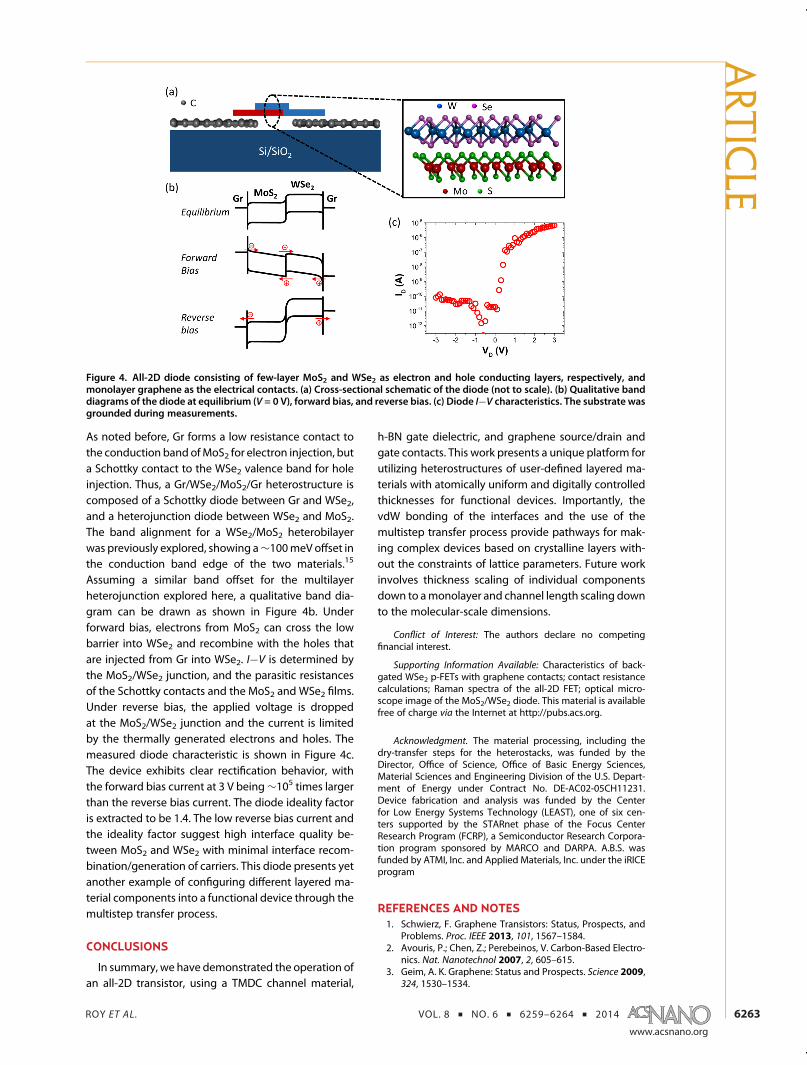
as the hole conducting layer, MoS2 as the electronconducting layer, and Gr as the contacts (Figure 4a).
Figure 3. All-2D MoS2 FET with few-layer h-BN gate dielectric, and bilayer graphene source/drain and multilayer graphenetop-gate electrodes. (a) Device schematic (not to scale). (b) IDVG characteristics at different VD. (c) IDVD characteristics. (d)Extracted mobility as a function of gate voltage, VG Vt. The inset shows the circuit model of the device used for mobilityextraction. The substrate is grounded during all measurements.
ARTIC
LE
ROY ET AL. VOL. 8 ’ NO. 6 ’ 6259–6264 ’ 2014
www.acsnano.org
6263
As noted before, Gr forms a low resistance contact tothe conduction band ofMoS2 for electron injection, buta Schottky contact to the WSe2 valence band for holeinjection. Thus, a Gr/WSe2/MoS2/Gr heterostructure iscomposed of a Schottky diode between Gr and WSe2,and a heterojunction diode between WSe2 and MoS2.The band alignment for a WSe2/MoS2 heterobilayerwas previously explored, showing a∼100meV offset inthe conduction band edge of the two materials.15
Assuming a similar band offset for the multilayerheterojunction explored here, a qualitative band dia-gram can be drawn as shown in Figure 4b. Underforward bias, electrons from MoS2 can cross the lowbarrier into WSe2 and recombine with the holes thatare injected from Gr into WSe2. IV is determined bythe MoS2/WSe2 junction, and the parasitic resistancesof the Schottky contacts and the MoS2 and WSe2 films.Under reverse bias, the applied voltage is droppedat the MoS2/WSe2 junction and the current is limitedby the thermally generated electrons and holes. Themeasured diode characteristic is shown in Figure 4c.The device exhibits clear rectification behavior, withthe forward bias current at 3 V being∼105 times largerthan the reverse bias current. The diode ideality factoris extracted to be 1.4. The low reverse bias current andthe ideality factor suggest high interface quality be-tween MoS2 and WSe2 with minimal interface recom-bination/generation of carriers. This diode presents yetanother example of configuring different layered ma-terial components into a functional device through themultistep transfer process.
CONCLUSIONS
In summary, we have demonstrated the operation ofan all-2D transistor, using a TMDC channel material,
h-BN gate dielectric, and graphene source/drain andgate contacts. This work presents a unique platform forutilizing heterostructures of user-defined layered ma-terials with atomically uniform and digitally controlledthicknesses for functional devices. Importantly, thevdW bonding of the interfaces and the use of themultistep transfer process provide pathways for mak-ing complex devices based on crystalline layers with-out the constraints of lattice parameters. Future workinvolves thickness scaling of individual componentsdown to amonolayer and channel length scaling downto the molecular-scale dimensions.
Conflict of Interest: The authors declare no competingfinancial interest.
Supporting Information Available: Characteristics of back-gated WSe2 p-FETs with graphene contacts; contact resistancecalculations; Raman spectra of the all-2D FET; optical micro-scope image of the MoS2/WSe2 diode. This material is availablefree of charge via the Internet at http://pubs.acs.org.
Acknowledgment. The material processing, including thedry-transfer steps for the heterostacks, was funded by theDirector, Office of Science, Office of Basic Energy Sciences,Material Sciences and Engineering Division of the U.S. Depart-ment of Energy under Contract No. DE-AC02-05CH11231.Device fabrication and analysis was funded by the Centerfor Low Energy Systems Technology (LEAST), one of six cen-ters supported by the STARnet phase of the Focus CenterResearch Program (FCRP), a Semiconductor Research Corpora-tion program sponsored by MARCO and DARPA. A.B.S. wasfunded by ATMI, Inc. and Applied Materials, Inc. under the iRICEprogram
REFERENCES AND NOTES1. Schwierz, F. Graphene Transistors: Status, Prospects, and
Problems. Proc. IEEE 2013, 101, 1567–1584.2. Avouris, P.; Chen, Z.; Perebeinos, V. Carbon-Based Electro-
nics. Nat. Nanotechnol 2007, 2, 605–615.3. Geim, A. K. Graphene: Status and Prospects. Science 2009,
324, 1530–1534.
Figure 4. All-2D diode consisting of few-layer MoS2 and WSe2 as electron and hole conducting layers, respectively, andmonolayer graphene as the electrical contacts. (a) Cross-sectional schematic of the diode (not to scale). (b) Qualitative banddiagrams of the diode at equilibrium (V = 0 V), forward bias, and reverse bias. (c) Diode IV characteristics. The substrate wasgrounded during measurements.
ARTIC
LE

ROY ET AL. VOL. 8 ’ NO. 6 ’ 6259–6264 ’ 2014
www.acsnano.org
6264
4. Liu, H.; Ye, P. D. MoS2 Dual-Gate MOSFET With Atomic-Layer-Deposited Al2O3 as Top-Gate Dielectric. IEEE ElectronDevice Lett. 2012, 33, 546–548.
5. Wang, H.; Yu, L.; Lee, Y.-H.; Shi, Y.; Hsu, A.; Chin, M. L.; Li, L.-J.;Dubey, M.; Kong, J.; Palacios, T. Integrated Circuits Basedon Bilayer MoS2 Transistors. Nano Lett. 2012, 12, 4674–4680.
6. Liu, H.; Xu, K.; Zhang, X.; Ye, P. D. The Integration of High-kDielectric on Two-Dimensional Crystals by Atomic LayerDeposition. Appl. Phys. Lett. 2012, 100–104.
7. Wei, L.; Jiahao, K.; Wei, C.; Sarkar, D.; Khatami, Y.; Jena, D.;Banerjee, K. High-Performance Few-Layer-MoS2 Field-Effect-Transistor with Record LowContact-Resistance. IEEEInt. Electron Devices Meet. 2013, 19.4.1–19.4.4.
8. Fang, H.; Tosun, M.; Seol, G.; Chang, T. C.; Takei, K.; Guo, J.;Javey, A. Degenerate n-Doping of Few-Layer TransitionMetal Dichalcogenides by Potassium. Nano Lett. 2013, 13,1991–1995.
9. Fang, H.; Chuang, S.; Chang, T. C.; Takei, K.; Takahashi, T.;Javey, A. High-Performance Single Layered WSe2 p-FETswith Chemically Doped Contacts. Nano Lett. 2012, 12,3788–3792.
10. Radisavljevic, B.; Whitwick, M. B.; Kis, A. Integrated Circuitsand Logic Operations Based on Single-Layer MoS2. ACSNano 2011, 5, 9934–9938.
11. Chuang, S.; Battaglia, C.; Azcatl, A.; McDonnell, S.; Kang,J. S.; Yin, X.; Tosun, M.; Kapadia, R.; Fang, H.; Wallace, R. M.;Javey, A. MoS2 P-type Transistors and Diodes Enabled byHigh Work Function MoOx Contacts. Nano Lett. 2014, 14,1337–1342.
12. Das, S.; Chen, H.-Y.; Penumatcha, A. V.; Appenzeller, J. HighPerformance Multilayer MoS2 Transistors with ScandiumContacts. Nano Lett. 2013, 13, 100–105.
13. Jena, D. Tunneling Transistors Based onGraphene and 2-DCrystals. Proc. IEEE 2013, 101, 1585–1602.
14. Cheng, R.; Li, D.; Zhou, H.; Wang, C.; Yin, A.; Jiang, S.; Liu, Y.;Chen, Y.; Huang, Y.; Duan, X. Electroluminescence and Pho-tocurrent Generation from Atomically Sharp WSe2/MoS2Heterojunction p-n Diodes. 2014, No. arXiv:1403.3447.
15. Fang, H.; Battaglia, C.; Carraro, C.; Nemsak, S.; Ozdol, B.;Kang, J. S.; Bechtel, H. A.; Desai, S. B.; Kronast, F.; Unal, A. A.;et al. Strong Interlayer Coupling in van der Waals Hetero-structures Built from Single-Layer Chalcogenides. Proc.Natl. Acad. Sci. U.S. A. 2014, 111, 6198–6202.
16. Baugher, B.W. H.; Chuchill, H. O. H.; Yang, Y.; Jarillo-Herrero,P. Optoelectronic Devices Based on Electrically Tunablep-n Diodes in a Monolayer Dichalcogenide. Nat. Nano-technol. 2014, 9, 262–267.
17. Yoon, J.; Park, W.; Bae, G.-Y.; Kim, Y.; Jang, H. S.; Hyun, Y.;Lim, S. K.; Kahng, Y. H.; Hong, W.-K.; Lee, B. H.; Ko, H. C.Highly Flexible and Transparent Multilayer MoS2 Transis-tors with Graphene Electrodes. Small 2013, 9, 3295–3300.
18. Lee, G.-H.; Yu, Y.-J.; Cui, X.; Petrone, N.; Lee, C.-H.; Choi, M. S.;Lee, D.-Y.; Lee, C.; Yoo, W. J.; Watanabe, K.; Taniguchi, T.;et al. Flexible and Transparent MoS2 Field-Effect Transis-tors on Hexagonal Boron Nitride-Graphene Heterostruc-tures. ACS Nano 2013, 7, 7931–7936.
19. Bertolazzi, S.; Krasnozhon, D.; Kis, A. Nonvolatile MemoryCells Based on MoS2/Graphene Heterostructures. ACSNano 2013, 7, 3246–3252.
20. Britnell, L.; Gorbachev, R. V.; Jalil, R.; Belle, B. D.; Schedin, F.;Mishchenko, A.; Georgiou, T.; Katsnelson, M. I.; Eaves, L.;Morozov, S. V.; et al. Field-Effect Tunneling TransistorBased on Vertical Graphene Heterostructures. Science2012, 335, 947–950.
21. Britnell, L.; Gorbachev, R. V.; Geim, A. K.; Ponomarenko,L. A.; Mishchenko, A.; Greenaway, M. T.; Fromhold, T. M.;Novoselov, K. S.; Eaves, L. Resonant Tunnelling and Nega-tive Differential Conductance in Graphene Transistors.Nat. Commun. 2013, 4, No. 1794.
22. Georgiou, T.; Jalil, R.; Belle, B. D.; Britnell, L.; Gorbachev,R. V.; Morozov, S. V.; Kim, Y.-J.; Gholinia, A.; Haigh, S. J.;Makarovsky, O.; et al. Vertical Field-Effect Transistor Basedon graphene-WS2 Heterostructures for Flexible and Trans-parent Electronics. Nat. Nanotechnol 2013, 8, 100–103.
23. Chuang, S.; Kapadia, R.; Fang, H.; Chang, T. C.; Yen, W.-C.;Chueh, Y.-L.; Javey, A. Near-ideal Electrical Properties ofInAs/WSe2 van der Waals Heterojunction Diodes. Appl.Phys. Lett. 2013, 102–105.
24. Rance, G. A.; Marsh, D. H.; Bourne, S. J.; Reade, T. J.;Khlobystov, A. N. van der Waals Interactions betweenNanotubes and Nanoparticles for Controlled Assemblyof Composite Nanostructures. ACS Nano 2010, 4, 4920–4928.
25. Ponomarenko, L. A.; Geim, A. K.; Zhukov, A. A.; Jalil, R.;Morozov, S. V.; Novoselov, K. S.; Grigorieva, I. V.; Hill, E. H.;Cheianov, V. V.; Fal'ko, V. I.; et al. Tunable Metal-InsulatorTransition in Double-Layer Graphene Heterostructures.Nat. Phys. 2011, 7, 958–961.
26. Dean, C. R.; Young, A. F.; Meric, I.; Lee, C.; Wang, L.;Sorgenfrei, S.; Watanabe, K.; Taniguchi, T.; Kim, P.; Shepard,K. L.; et al. Boron Nitride Substrates for High-QualityGraphene Electronics.Nat. Nanotechnol. 2010, 5, 722–726.
27. Chan, J.; Venugopal, A.; Pirkle, A.; McDonnell, S.; Hinojos, D.;Magnuson, C. W.; Ruoff, R. S.; Colombo, L.; Wallace, R. M.;Vogel, E. M. Reducing Extrinsic Performance-LimitingFactors in Graphene Grown by Chemical Vapor Deposi-tion. ACS Nano 2012, 6, 3224–3229.
28. Suk, J. W.; Kitt, A.; Magnuson, C. W.; Hao, Y.; Ahmed, S.; An,J.; Swan, A. K.; Goldberg, B. B.; Ruoff, R. S. Transfer of CVD-Grown Monolayer Graphene onto Arbitrary Substrates.ACS Nano 2011, 5, 6916–6924.
29. Khomyakov, P. A.; Giovannetti, G.; Rusu, P. C.; Brocks, G.;van den Brink, J.; Kelly, P. J. First-Principles Study of theInteraction and Charge Transfer between Graphene andMetals. Phys. Rev. B 2009, 79, 195425.
30. Liu, H.; Liu, Y.; Zhu, D. Chemical Doping of Graphene.J. Mater. Chem. 2011, 21, 3335–3345.
31. Radisavljevic, B.; Radenovic, A.; Brivio, J.; Giacometti, V.; Kis,A. Single-Layer MoS2 Transistors. Nat. Nanotechnol. 2011,6, 147–150.
32. Jin, S.; Fischetti, M. V.; Tang, T.-W. Modeling of Surface-Roughness Scattering in Ultrathin-Body SOIMOSFETs. IEEETrans. Electron Devices 2007, 54, 2191–2203.
33. Takei, K.; Kapadia, R.; Fang, H.; Plis, E.; Krishna, S.; Javey, A.High Quality Interfaces of InAs-on-Insulator Field-EffectTransistors with ZrO2 Gate Dielectrics. Appl. Phys. Lett.2013, 102–105.
ARTIC
LE

S1
Field-Effect Transistors Built from All Two-
Dimensional Material Components
Tania Roy,1,2,3
Mahmut Tosun,1,2,3
Jeong Seuk Kang,1,2,3
Angada B. Sachid,1 Sujay B.
Desai, 1,2,3
Mark Hettick,1,2,3
Chenming C. Hu1, and Ali Javey
1,2,3,†
1Electrical Engineering and Computer Sciences, University of California, Berkeley, CA,
94720.
2Materials Sciences Division, Lawrence Berkeley National Laboratory, Berkeley, CA
94720.
3Berkeley Sensor and Actuator Center, University of California, Berkeley, CA, 94720.
† Corresponding Author: [email protected]
Supporting Information

S2
WSe2 Schottky-barrier FETs with monolayer graphene contacts
Figure S1 shows the ID-VDS, and ID-VGS characteristics of a back-gated FET with WSe2
channel and monolayer graphene contacts. The WSe2 flake is ~5 nm thick. The length
and width of the device are 7 µm and 18 µm, respectively. Graphene forms a Schottky
contact with the valence band of WSe2, allowing for injection of holes but with a high
contact resistance. Here, the p+ Si substrate is used as the back-gate with 260 nm thick
SiO2 as the gate dielectric.
Figure S1. Back-gated WSe2 FET with graphene contacts. (a) Schematic of WSe2 p-FET
with graphene contacts. (b) ID-VD characteristics. (c) ID-VG characteristics.

S3
Contact resistance extraction of All-2D FET
Figure S2 shows the total resistance, Rtot, vs. VGS curve, extracted from the I-V curves of
the all-2D n-FET of Figure 3. Rtot is obtained from VD/ID at VD = 0.08 V. Since only a
limited number of data points were available for gate voltage, VGS, the Rtot vs. VGS curve
is extrapolated using the polynomial b1+b2/x+b3/x2
, where the fitting parameters are
extracted as:
b1 = 29898 = 2Rc
b2 = 4.15895×10⁵
b3 = -4.90489×10⁵
As VGS approaches ∞, Rtotal approached 2Rc, since the channel resistance decreases
substantially. Rc is thus extracted to be ~15 kΩ.
Figure S2: Rtot vs. VGS for the all-2D FET of Figure 3 used to extract Rc.
20 40 60 80 100
20
40
60
80
100
120
Rtot (kΩΩ ΩΩ)
VGS (V)

S4
Raman spectroscopy of layered components in all-2D FET of Fig.1
Figure S3. (a) Optical image of the all-2D FET of Fig. 1 of main text, showing the points
where Raman scan was performed. (b) Raman spectrum at point (i), as marked in panel
(a), where MoS2, h-BN and exfoliated graphene are present. (c) Raman spectrum at point
(ii), where only h-BN is present. (d) Raman spectrum at point (iii), showing the presence
of bilayer graphene. (e) Raman spectrum at point (iv), showing the presence of bilayer
graphene.
S5
Optical microscope image of MoS2/WSe2 heterojunction diode with monolayer graphene
contacts of device shown in Fig. 4
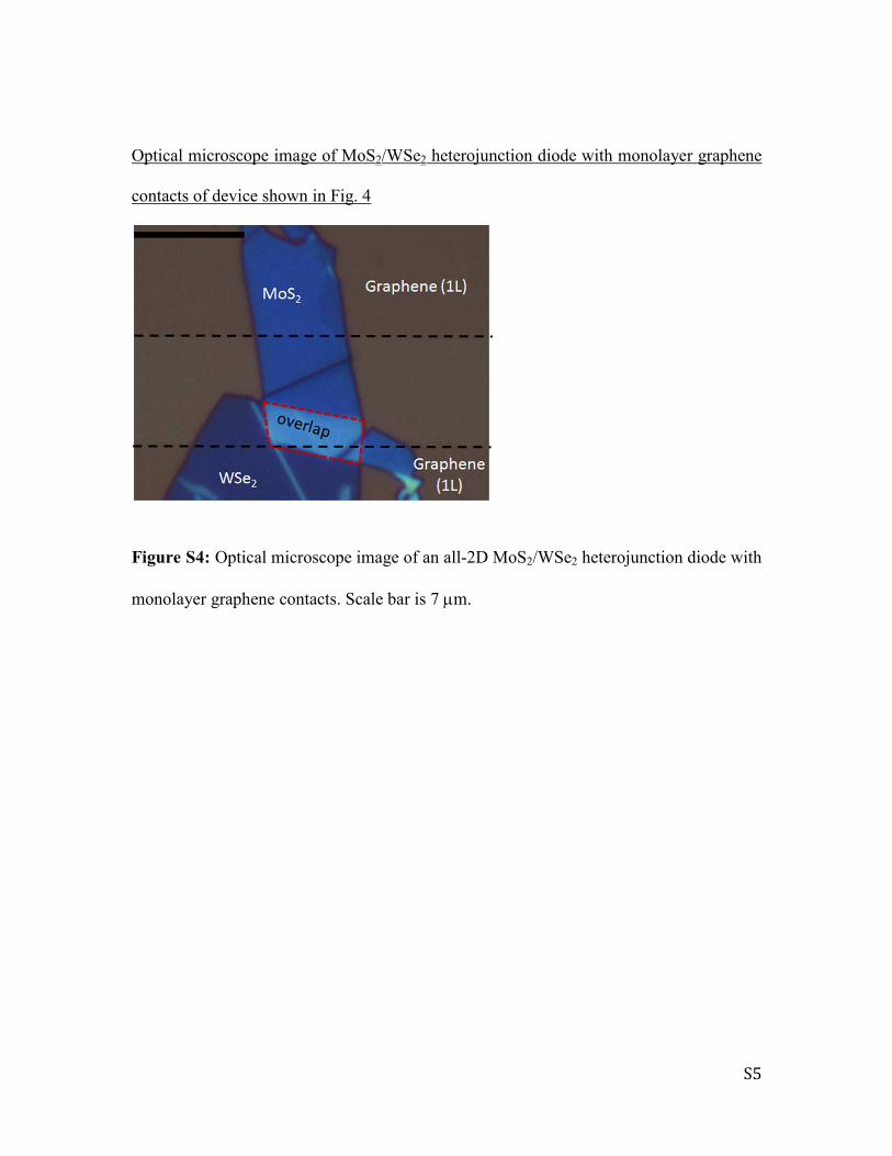
Figure S4: Optical microscope image of an all-2D MoS2/WSe2 heterojunction diode with
monolayer graphene contacts. Scale bar is 7 µm.