tft 17mb20 sm
TRANSCRIPT


1. INTRODUCTION....................................................................................................................... 3 2. AUDIO AMPLIFIER STAGE WITH TDA2822M.................................................................... 3 4. TUNER........................................................................................................................................ 5
General description of UV1316: ............................................................................................. 5 Features of UV1316: ............................................................................................................... 5
5. MICROCONTROLLER (VCTI) ................................................................................................ 5 General Features...................................................................................................................... 5 DRX Features.......................................................................................................................... 6 Multistandard Sound Processor (MSP) Features .................................................................... 7 Video Features......................................................................................................................... 8 Controller Features.................................................................................................................. 9 OSD & Teletext Features ........................................................................................................ 9 Port Allocation ...................................................................................................................... 10
6. SCALER & DEINTERLACER (TSU) ..................................................................................... 13 General Features.................................................................................................................... 13 Display Features................................................................................................................... 13 Auto Detection Features........................................................................................................ 14 OSD Features ........................................................................................................................ 14
7. SAW FILTER ........................................................................................................................... 14 X6897D: ................................................................................................................................ 14 Standard:................................................................................................................................ 14 Features: ................................................................................................................................ 14 Pin configuration: .................................................................................................................. 15 Frequency response: .............................................................................................................. 15
8. IC SPECIFICATIONS ............................................................................................................. 17 8.1. LM1117.......................................................................................................................... 17 8.2. LM1086.......................................................................................................................... 18 8.3. LM317............................................................................................................................ 20 8.4. MP1593 .......................................................................................................................... 20 8.5. IRF7314.......................................................................................................................... 23 8.6. FDC642P........................................................................................................................ 24 8.7. NTGS3446 ..................................................................................................................... 25 8.8. 74HCT4053.................................................................................................................... 26
9.OPEN-SHORT CIRCUIT PROTECTION ................................................................................ 34 10.SERVİCE MENU SETTINGS..................................................................................................35 11. BLOCK DIAGRAM AND SCHEMATICS............................................................................40

1. INTRODUCTION 17MB20 Main Board consists of two major blocks. The first block is analog front-end and this block is handled by highly multifunctional VCTI49XY chip. This IC performs demodulation of Video & Audio from Tuner IF, and CVBS, Audio, RGB, SVHS input selection and processing. It has an audio processor that supports equalizer or tone control, volume control, AVL, surround effect etc. and supplies audio outputs for audio amplifier, scart and line out. It handles video processing such as colour standard detection and demodulation, picture alignment (brightness, contrast, colour etc.). The IC also performs teletext decoding with fastext memory. The processed video is sent to TSU36AWL-M(-1) chip in RGB format and to the scart video output in CVBS format. The TV Tuner is a PLL controlled asymmetrical or a symmetrical IF output type. The IF signal is applied to a single saw filter. After the SAW filter block, VSB modulated sound and picture signals are digitally filtered and demodulated by VCTI. Since VCTI handles all audio processing issues, there is no need for additional audio processor solution on the board. VCTI supports three Audio outputs. These outputs are assigned to audio amplifier, scart audio out and line out. The board employs TDA2822M Class AB Audio Amplifier to drive both the speaker and headphone outputs. The Back End section is handled by TSU36AWL-M(-1) chip. TSU has two ADC inputs. The ADC inputs can handle standard interlaced RGB output from VCTI, PC RGB graphics input and YPbPr input via VGA Connector. ADC0 is assigned to YPbPr input or RGB input via VGA connector and ADC1 is assigned to VCTI RGB output. Scaling and deinterlacing is performed in Back End. TSU chip has an integrated LVDS transmitter which provides double LVDS output support. Backlight brightness level adjustment and backlight on/off control for the inverter, and Panel Logic Circuitry Power on/off control is performed by TSU chip. OSD is displayed by the OSD generator embedded in TSU chip.
2. AUDIO AMPLIFIER STAGE WITH TDA2822M The system is designed with 2XTDA2822M audio amplifiers for main speaker and headphone L/R outputs. There is no any other dedicated audio amplifier for the headphone audio output. In order to switch the audio amplifier output to the speakers or headphone, the headphone output jack is detached for all TV sets with headphone output option. The TDA2822M is a monolithic integrated circuit in 8 leap minidip package, intended for use as low frequency Class AB power amplifier in a wide range of applications in radio and TV sets. For left and right channels two TDA2822M audio amplifiers are used in bridge mode operation to provide 2x2W audio output power with 16 Ohm Speakers at %10 THD.
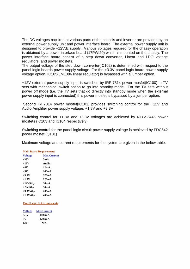
The DC voltages required at various parts of the chassis and inverter are provided by an external power supply unit and power interface board. The external power supply unit is designed to provide +12Vdc supply. Various voltages required for the chassy operation is obtained by a power interface board (17PWI20) which is mounted on the chassy. The power interface board consist of a step down converter, Linear and LDO voltage regulators, and power mosfets. The output voltage of the step down converter(IC102) is determined with respect to the panel logic boards power supply voltage. For the +3.3V panel logic board power supply voltage option, IC105(LM1086 linear regulator) is bypassed with a jumper option. +12V external power supply input is switched by IRF 7314 power mosfet(IC100) in TV sets with mechanical switch option to go into standby mode. For the TV sets without power off mode (i.e. the TV sets that go directly into standby mode when the external power supply input is connected) this power mosfet is bypassed by a jumper option. Second IRF7314 power mosfet(IC101) provides switching control for the +12V and Audio Amplifier power supply voltage. +1,8V and +3.3V Switching control for +1.8V and +3.3V voltages are achieved by NTGS3446 power mosfets (IC103 and IC104 respectively) Switching control for the panel logic circuit power supply voltage is achieved by FDC642 power mosfet (Q101) Maximum voltage and current requirements for the system are given in the below table. Main Board Requirements Voltage Max Current +33V 5mA +12V Audio +8V 12mA +5V 160mA +3.3V 370mA +1.8V 220mA +12VStby 30mA + 5VStby 30mA +3.3Vstby 205mA +1.8Vstby 400mA Panel Logic Cct Requirments Voltage Max Current 3.3V 1100mA 5V 1200mA 12V N/A
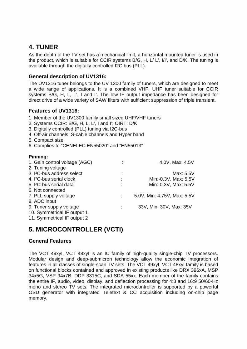
4. TUNER As the depth of the TV set has a mechanical limit, a horizontal mounted tuner is used in the product, which is suitable for CCIR systems B/G, H, L/ L’, I/I’, and D/K. The tuning is available through the digitally controlled I2C bus (PLL).
General description of UV1316: The UV1316 tuner belongs to the UV 1300 family of tuners, which are designed to meet a wide range of applications. It is a combined VHF, UHF tuner suitable for CCIR systems B/G, H, L, L’, I and I’. The low IF output impedance has been designed for direct drive of a wide variety of SAW filters with sufficient suppression of triple transient.
Features of UV1316: 1. Member of the UV1300 family small sized UHF/VHF tuners 2. Systems CCIR: B/G, H, L, L’, I and I’; OIRT: D/K 3. Digitally controlled (PLL) tuning via I2C-bus 4. Off-air channels, S-cable channels and Hyper band 5. Compact size 6. Complies to “CENELEC EN55020” and “EN55013” Pinning: 1. Gain control voltage (AGC) : 4.0V, Max: 4.5V 2. Tuning voltage 3. I²C-bus address select : Max: 5.5V 4. I²C-bus serial clock : Min:-0.3V, Max: 5.5V 5. I²C-bus serial data : Min:-0.3V, Max: 5.5V 6. Not connected 7. PLL supply voltage : 5.0V, Min: 4.75V, Max: 5.5V 8. ADC input 9. Tuner supply voltage : 33V, Min: 30V, Max: 35V 10. Symmetrical IF output 1 11. Symmetrical IF output 2
5. MICROCONTROLLER (VCTI) General Features The VCT 49xyI, VCT 48xyI is an IC family of high-quality single-chip TV processors. Modular design and deep-submicron technology allow the economic integration of features in all classes of single-scan TV sets. The VCT 49xyI, VCT 48xyI family is based on functional blocks contained and approved in existing products like DRX 396xA, MSP 34x5G, VSP 94x7B, DDP 3315C, and SDA 55xx. Each member of the family contains the entire IF, audio, video, display, and deflection processing for 4:3 and 16:9 50/60-Hz mono and stereo TV sets. The integrated microcontroller is supported by a powerful OSD generator with integrated Teletext & CC acquisition including on-chip page memory.

– Submicron CMOS technology – Low-power standby mode – Single 20.25 MHz reference crystal – 8-bit 8051 instruction set compatible CPU – Up to 256 kB on-chip program ROM – WST, PDC, VPS, and WSS acquisition – Up to 10 pages on-chip teletext memory – Multi-standard QSS IF processing with single SAW – FM Radio and RDS with standard TV tuner – TV-sound demodulation: • all A2 standards • all NICAM standards • BTSC/SAP with MNR (DBX optional) • EIA-J – Baseband sound processing for loudspeaker channel: • volume and balance • bass/treble or equalizer • loudness and spatial effect (e.g. pseudo stereo) • Micronas AROUND (virtual Dolby optional) • Micronas BASS and Subwoofer output • further optional and licence requiring sound enhancements as BBE, SRS Wow – CVBS, S-VHS, YCbCr and RGB inputs – ITU656 input – 4H adaptive comb filter (PAL/NTSC) – multi-standard color decoder (PAL/NTSC/SECAM) – Macrovision Detection – Nonlinear horizontal scaling “panorama vision” – Luma and chroma transient improvement (LTI, CTI) – Non-linear color space enhancement (NCE) – Dynamic black level expander (BLE) – Selective Color Enhancer (SCE) – 8/10 bit ITU656 output – Soft start/stop of H-drive
DRX Features The DRX - Analog TV IF- Demodulator performs the entire multistandard Quasi Split Sound (QSS) TV IF processing, AGC, video demodulation, and generation of the second sound IF (SIF) requiring only one SAW filter. The alignment-free DRX does not need special external components. All control functions and status registers are accessible via I2C bus interface. Therefore, it simplifies the design of high-quality, highly standardized IF stages. – Multistandard QSS IF processing with a single SAW – Highly reduced amount of external components (no tank circuit, no potentiometers, no
SAW switching) – Programmable IF frequency (38.9 MHz, 45.75 MHz, 32.9 MHz, 58.75 MHz, 36.125 MHz) – Digital IF processing for the following standards: B/G, D/K, I, L/L’, and M/N – Standard specific digital post filtering – Standard specific digital video/audio splitting – Standard specific digital picture carrier recovery: • alignment-free • quartz-stable and accurate • stable frequency lock at 100% modulation and overmodulation up to 150% • quartz-accurate AFC information – Programmable standard specific digital group delay equalization – Automatically frequency-adjusted Nyquist slope, therefore optimal picture and sound performance over complete lock in frequency range – Standard-specific digital AGC and delayed tuner AGC with programmable tuner Take Over Point
Multistandard Sound Processor (MSP) Features The MSP receives the digital Sound IF signal from the DRX part. The MSP is able to demodulate all TV sound standards worldwide including the digital NICAM system. Depending on the VCTI version, the following demodulation modes can be performed. TV stereo sound standards that are unavailable for a specific VCTI version are processed in analog mono sound of the standard. In that case, stereo or bilingual processing will not be possible. – Sound demodulator and stereo decoder – Audio processing for loudspeaker channels:
• volume • Automatic Volume Correction (AVC) • bass/treble or equalizer • loudness • balance • configurable Subwoofer output
– Optional features for loudspeaker channels: • Virtual Dolby Surround (VDS) • SRS WOW • BBE High Definition Sound
– PMQFP144-2 package: • 6 analog audio inputs • 4 analog audio outputs
– PSSDIP88-1 package: • 4 analog audio inputs • 2 analog audio outputs • 2 configurable analog audio inputs/outputs

Video Features The TVT is a Teletext decoder for decoding World System Teletext data, as well as Video Programming System (VPS), Program Delivery Control (PDC), and Wide-Screen Signalling (WSS) data used for PALplus transmissions (line 23). The device also supports Closed Caption acquisition and decoding. The TVT provides an integrated general-purpose, fully 8051-compatible microcontroller with television-specific hardware features. The microcontroller has been enhanced to provide powerful features such as memory banking, data pointer, additional interrupts, etc. The on-chip display unit for displaying Level 1.5 Teletext data can also be used for customer-defined onscreen displays. The TVT has an internal XRAM of 20 KB and an internal ROM of up to 256 KB. ROMless versions can address up to 1 MB of external RAM and ROM. The 8-bit microcontroller runs at 296 ns cycle time. The controller with dedicated hardware does most of the internal TTX acquisition processing, transfers data to/from external memory interface, and receives/transmits data via I2C-bus interface. In combination with dedicated hardware, the slicer stores TTX data in a VBI buffer of 1 KB. The microcontroller firmware performs all the acquisition tasks (hamming and parity checks, page search, and evaluation of header control bits) once per field. Additionally, the firmware can provide high-end Teletext features like Packet-26 handling, FLOF/TOP and list-pages. The interface-to-user software is optimized for minimal overhead. TVT is realized in deep submicron technology with 1.8 V supply voltage and 3.3 V I/O (TTL compatible). – 11 analog video inputs (CVBS/Y/C/RGB/YCbCr) – 3 analog video outputs – integrated Y+C adder – integrated high-quality A/D converters and associated clamp and AGC circuits – high-performance 4H comb filter (PAL/NTSC) with vertical peaking – multistandard color decoder PAL/NTSC/SECAM including all substandards – macrovision-compliant multistandard sync processing – macrovision detection – RGB/YCbCr component processing and associated contrast, color saturation and tint circuits – high-quality soft mixer controlled by fast blank (alpha blending) – fast blank monitor via I2C – ITU656 input – linear horizontal scaling (0.25 to 4) – nonlinear horizontal scaling “panorama vision” – split screen (OSD and video side by side) – letter box detector (auto-wide) – noise measurement

Controller Features The TVT is a Teletext decoder for decoding World System Teletext data, as well as Video Programming System (VPS), Program Delivery Control (PDC), and Wide-Screen Signalling (WSS) data used for PALplus transmissions (line 23). The device also supports Closed Caption acquisition and decoding. The TVT provides an integrated general-purpose, fully 8051-compatible microcontroller with television-specific hardware features. The microcontroller has been enhanced to provide powerful features such as memory banking, data pointer, additional interrupts, etc. – Single external 20.25 MHz crystal, all necessary clocks are generated internally – Normal mode: 40.5 MHz CPU clock, Power Save mode: 10.125 MHz – Up to 256 KB on-chip program ROM – 256 byte on-chip program RAM – 128 byte on-chip extended stack RAM – 20 kilobyte on-chip extended data RAM (XRAM) – Memory banking up to 1 MB – Non-multiplexed 8-bit data and 20-bit address bus – Eight 16-bit data pointer registers (DPTR) – 4-level, 24-input interrupt controller – Patch module for 16 ROM locations – Two 16-bit reloadable timers – Capture-compare timer for infrared decoding – Watchdog timer – UART – Real time clock (RTC) – PWM units (2 channels 14-bit, 6 channels 8-bit) – 8-bit ADC (4 channels) – I2C bus master/slave interface – Up to 24 programmable I/O ports – Flash version for PMQFP144 and PSSDIP88 packages (SST39LF020 or compatible) – ROM-less version with 1 MB address space for external program and data memory
OSD & Teletext Features The on-chip display unit for displaying Level 1.5 Teletext data can also be used for customer-defined onscreen displays. The TVT has an internal XRAM of 20 KB and an internal ROM of up to 256 KB. ROMless versions can address up to 1 MB of external RAM and ROM. In combination with dedicated hardware, the slicer stores TTX data in a VBI buffer of 1 KB. The microcontroller firmware performs all the acquisition tasks (hamming and parity checks, page search, and evaluation of header control bits) once per field. Additionally, the firmware can provide high-end Teletext features like Packet-26 handling, FLOF/TOP and list-pages. The interface-to-user software is optimized for minimal overhead.

Port Allocation


6. SCALER & DEINTERLACER (TSU) The are two pin compatible IC versions. TSU36AWL-M is a total solution graphics processing IC for LCD displays with panel resolutions up to SXGA(1280X1024), and TSU36AWL-M-1 provides support for resolutions up to SXGA+(1400X1050). TSU36AWL-M(-1) is configured with a high-speed integrated triple-ADC/PLL, a high quality display processing engine, and an integrated multi-purpose output display interface that can support all major panel interface formats. To further reduce system costs, the TSU36AWL-M(-1) also integrates intelligent power management control capability for green-mode requirements and spread-spectrum support for EMI management.
General Features - Two RGB analog input ports support up to 165 MHz (UXGA @ 60Hz) - Full SOG and composite sync support, including copy protected signals
Display Features - Patent-pending Hybrid Image Resolution Converter - Variable sharpness control - Interlaced to progressive conversion - Patent-pending Dynamic Frame-Rate generator (DFR) – short line storage frame extension technique eliminates short lines in output frames - Media Window Enhancement (MWE) - Peaking and coring functions for sharpness enhancement and noise reduction - Brightness and contrast control - Programmable 10-bit gamma correction - sRGB support
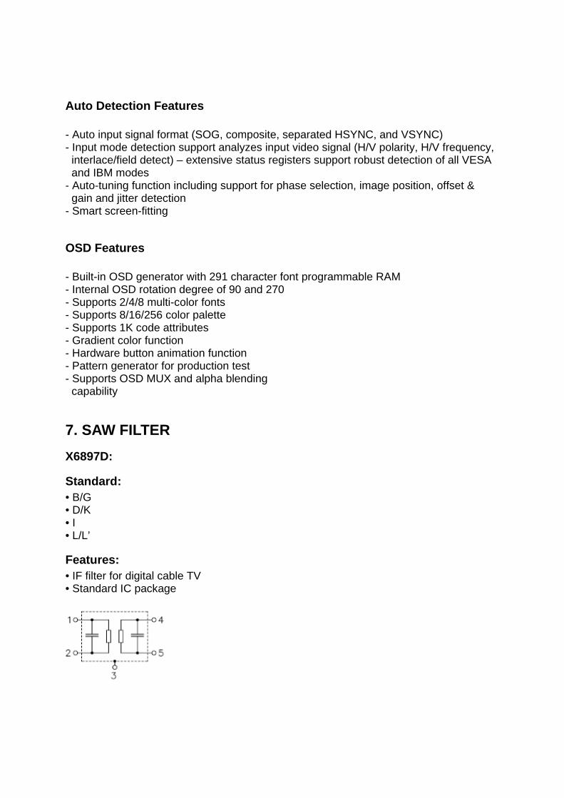
Auto Detection Features - Auto input signal format (SOG, composite, separated HSYNC, and VSYNC) - Input mode detection support analyzes input video signal (H/V polarity, H/V frequency, interlace/field detect) – extensive status registers support robust detection of all VESA and IBM modes - Auto-tuning function including support for phase selection, image position, offset & gain and jitter detection - Smart screen-fitting
OSD Features - Built-in OSD generator with 291 character font programmable RAM - Internal OSD rotation degree of 90 and 270 - Supports 2/4/8 multi-color fonts - Supports 8/16/256 color palette - Supports 1K code attributes - Gradient color function - Hardware button animation function - Pattern generator for production test - Supports OSD MUX and alpha blending capability
7. SAW FILTER X6897D:
Standard: • B/G • D/K • I • L/L’
Features: • IF filter for digital cable TV • Standard IC package

Pin configuration: 1 Input 2 Input - ground 3 Chip carrier - ground 4 Output 5 Output
Frequency response:


8. IC SPECIFICATIONS LM1117 LM1086 LM317 MP1593 IRF7314 FDC642P NTGS3446 74HCT4053 74HC4052 24C64 24LC21 TDA2822M
8.1. LM1117 8.1.1. General Description The LM1117 is a series of low dropout voltage regulators with a dropout of 1.2V at 800mA of load current. It has the same pin-out as National Semiconductor’s industry standard LM317. The LM1117 is available in an adjustable version, which can set the output voltage from 1.25V to 13.8V with only two external resistors. In addition, it is also available in five fixed voltages, 1.8V, 2.5V, 2.85V, 3.3V, and 5V. The LM1117 offers current limiting and thermal shutdown. Its circuit includes a zener trimmed bandgap reference to as-sure output voltage accuracy to within ±1%. The LM1117 series is available in SOT- 223, TO-220, and TO-252 D-PAK packages. A minimum of 10μF tantalum capacitor is required at the output to improve the transient response and stability. 8.1.2. Features • Available in 1.8V, 2.5V, 2.85V, 3.3V, 5V, and Adjustable Versions • Space Saving SOT-223 Package • Current Limiting and Thermal Protection • Output Current 800mA • Line Regulation 0.2% (Max) • Load Regulation 0.4% (Max) • Temperature Range — LM1117 0°C to 125°C — LM1117I -40°C to 125°C 8.1.3. Applications • 2.85V Model for SCSI-2 Active Termination • Post Regulator for Switching DC/DC Converter • High Efficiency Linear Regulators • Battery Charger • Battery Powered Instrumentation

8.1.4. Absolute Maximum Ratings
8.1.5. Connection Diagram
8.2. LM1086 8.2.1. General Description The LM1086 is a low dropout three terminal regulator with 1.5A output current capability. The output voltage is adjustable with the use of a resistor divider. Dropout is guaranteed at a maximum of 500 mV at maximum output current. It's low dropout voltage and fast transient response make it ideal for low voltage microprocessor applications. Internal current and thermal limiting provides protection against any overload condition that would create excessive junction temperature. 8.2.2. Features Low Dropout Voltage 500mV at 1.5A Output Current Fast Transient Response 0.015% Line Regulation 0.1% Load Regulation Internal Thermal and Current Limiting Adjustable or Fixed Output Voltage(1.5, 2.5, 2.85, 3.0, 3.3, 5.0V) Surface Mount Package SOT-223 & TO-263 (D2 Package) 100% Thermal Limit Burn-in 8.2.3. Applications Battery Charger Adjustable Power Supplies

Constant Current Regulators Portable Instrumentation High Efficiency Linear Power Supplies High Efficiency "Green" Computer Systems SMPS Post-Regulator Power PC Supplies Powering VGA & Sound Card 8.2.4. Absolute Maximum Ratings
8.2.5. Connection Diagrams

8.3. LM317 8.3.1. General Description The LM117/LM217/LM317 are monolithic integrated circuit in TO-220, ISOWATT220, TO-packages intended for use as positive adjustable voltage regulators. They are designed to supply more than 1.5A of load current with an output voltage adjustable 1.2 to 37V range. The nominal output voltage is selected by means of only a resistive divider, making exceptionally easy to use and eliminating the stocking of many fixed regulators. 8.3.2. Features Output voltage range: 1.2 to 37V Output current in excess of 1.5A 0.1% Line and Load Regulation Floating Operation for High Voltages Complete Series of Protections: Current Limiting, Thermal Shutdown and SOA Control 8.3.3. Connection Diagram
8.4. MP1593 8.4.1. General Description The MP1593 is a step-down converter with an internal Power MOSFET. It achieves 3A continuous output current over a wide input supply range with excellent load and line regulation. Current mode operation provides fast transient response and eases loop stabilization. Fault condition protection includes cycle-by-cycle current limiting and thermal shutdown. Adjustable soft-start reduces the stress on the input source at turn-on. In shutdown mode the regulator draws 20μA of supply current. The MP1593 requires a minimum number of readily available external components to complete a 3A step down DC to DC converter solution.

8.4.2. Features 3A Output Current Programmable Soft-Start 100mΩ Internal Power MOSFET Switch Stable with Low ESR Output Ceramic Capacitors Up to 95% Efficiency 20μA Shutdown Mode Fixed 385KHz Frequency Thermal Shutdown Cycle-by-Cycle Over Current Protection Wide 4.75 to 28V Operating Input Range Output Adjustable from 1.22V Under Voltage Lockout Available in 8-Pin SOIC Package 8.4.3. Applications Distributed Power Systems Battery Chargers Pre-Regulator for Linear Regulators Flat Panel TVs Set-Top Boxes Cigarette Lighter Powered Devices DVD/PVR Devices 8.4.4. Absolute Maximum Ratings
8.4.5. Electrical Characteristics

8.4.6. Pin Functions Pin1:BS High-Side Gate Drive Boost Input. BS supplies the drive for the high-side N-Channel MOSFET switch. Connect a 10nF or greater capacitor from SW to BS to power the high side switch. Pin2:IN Power Input. IN supplies the power to the IC, as well as the step-down converter switches. Drive IN with a 4.75V to 28V power source. Bypass IN to GND with a suitably large capacitor to eliminate noise on the input to the IC. Pin3:SW Power Switching Output. SW is the switching node that supplies power to the output. Connect the output LC filter from SW to the output load. Note that a capacitor is required from SW to BS to power the high-side switch. Pin4:GND Ground.

Pin5:FB Feedback Input. FB senses the output voltage to regulate that voltage. Drive FB with a resistive voltage divider from the output voltage. The feedback threshold is 1.222V. Pin6:COMP Compensation Node. COMP is used to compensate the regulation control loop. Connect a series RC network from COMP to GND to compensate the regulation control loop. In some cases, an additional capacitor from COMP to GND is required. Pin7:EN Enable Input. EN is a digital input that turns the regulator on or off. Drive EN high to turn on the regulator, drive EN low to turn it off. An Under Voltage Lockout (UVLO) function can be implemented by the addition of a resistor divider from VIN to GND. For complete low current shutdown its needs to be less than 0.7V. For automatic startup, leave EN unconnected. Pin8:SS Soft-Start Control Input. SS controls the soft-start period. Connect a capacitor from SS to GND to set the soft-start period. A 0.1μF capacitor sets the soft-start period to 10ms. To disable the soft-start feature, leave SS unconnected.
8.5. IRF7314 Fifth Generation HEXFETs from International Rectifier utilize advanced processing techniques to achieve extremely low on-resistance per silicon area. This benefit, combined with the fast switching speed and ruggedized device design that HEXFET Power MOSFETs are well known for, provides the designer with an extremely efficient and reliable device for use in a wide variety of applications. The SO-8 has been modified through a customized leadframe for enhanced thermal characteristics and multiple-die capability making it ideal in a variety of power applications. With these improvements, multiple devices can be used in an application with dramatically reduced board space. The package is designed for vapor phase, infra red, or wave soldering techniques.

8.5.1. Absolute Maximum Ratings 7314 (TA = 25°C Unless Otherwise Noted)
8.6. FDC642P 8.6.1. General Description This p-channel 2.5V specified MOSFET is produced using Fairchild’s advanced PowerTrench process that has been especially tailored to minimize on state resistance and yet maintain low gate charge for superior switching performance. 8.6.2 . Features
8.6.3. Absolute Maximum Ratings

8.6.4. Connection Diagram
8.7. NTGS3446 8.7.1. General Description NTGS3446 is an N-channel power mosfet with 5A continuous drain current and low Rds(on) voltage. 8.7.2 . Features
8.7.3. Absolute Maximum Ratings Tc=25C unless otherwise noted

8.7.4. Connection Diagram
8.8. 74HCT4053 8.8.1. General Description The 74HC/HCT4053 are high-speed Si-gate CMOS devices and are pin compatible with the “4053” of the “4000B” series. They are specified in compliance with JEDEC standard no. 7A. The 74HC/HCT4053 are triple 2-channel analog multiplexers/demultiplexers with a common enable input (E). Each multiplexer/demultiplexer has two independent

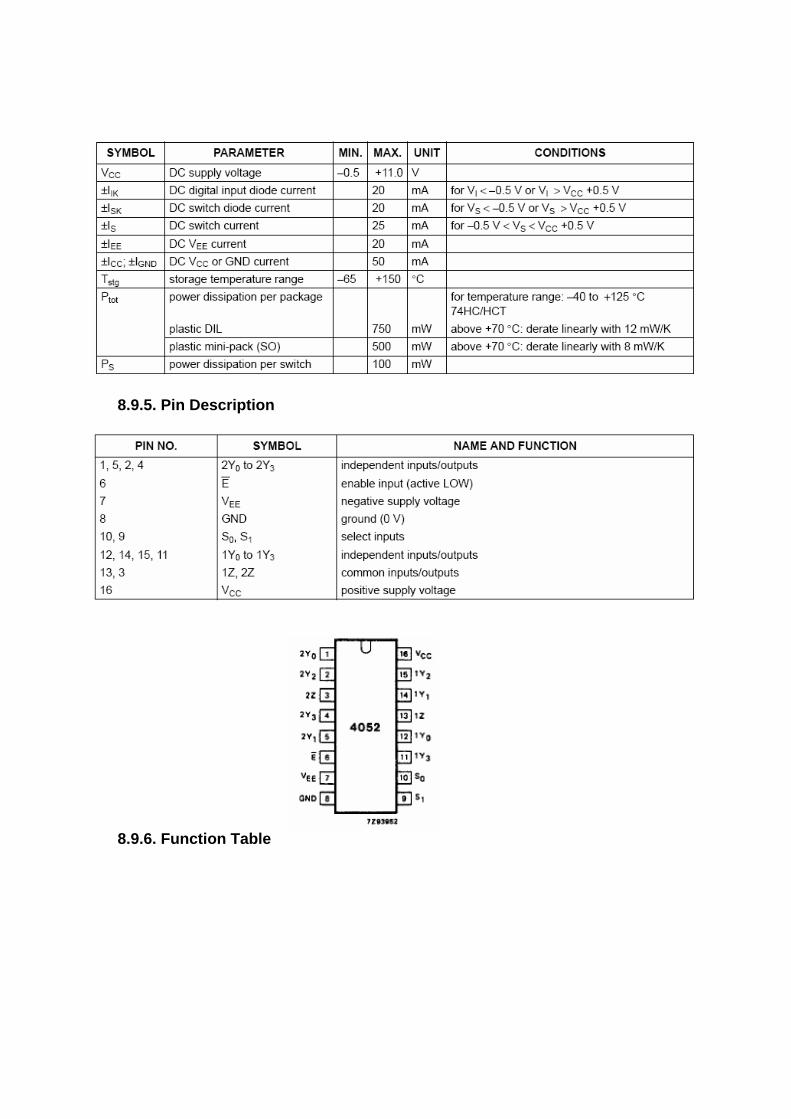
inputs/outputs (nY0 and nY1), a common input/output (nZ) and three digital select inputs (S1 to S3). With E LOW, one of the two switches is selected (low impedance ON-state) by S1 to S3. With E HIGH, all switches are in the high impedance OFF-state, independent of S1 to S3. VCC and GND are the supply voltage pins for the digital control inputs (S1, to S3, and E). The VCC to GND ranges are 2.0 to 10.0 V for HC and 4.5 to 5.5 V for HCT. The analog inputs/outputs (nY0 and nY1, and nZ) can swing between VCC as a positive limit and VEE as a negative limit. VCC - VEE may not exceed 10.0 V. For operation as a digital multiplexer/demultiplexer, VEE is connected to GND (typically ground). 8.8.2. Features Low “ON” resistance: 80 W (typ.) at VCC - VEE = 4.5 V 70 W (typ.) at VCC - VEE = 6.0 V 60 W (typ.) at VCC - VEE = 9.0 V Logic level translation:to enable 5 V logic to communicate with ± 5 V analog signals Typical “break before make” built in Output capability: non-standard ICC category: MSI 8.8.3. Applications Analog multiplexing and demultiplexing Digital multiplexing and demultiplexing Signal gating 8.8.4. Absolute Maximum Ratings
8.8.5. Pin Description

8.8.6. Function Table
8.9. 74HC4052 8.9.1. General Description The 74HC/HCT4052 are high-speed Si-gate CMOS devices and are pin compatible with the “4052” of the “4000B” series. They are specified in compliance with JEDEC standard no. 7A.
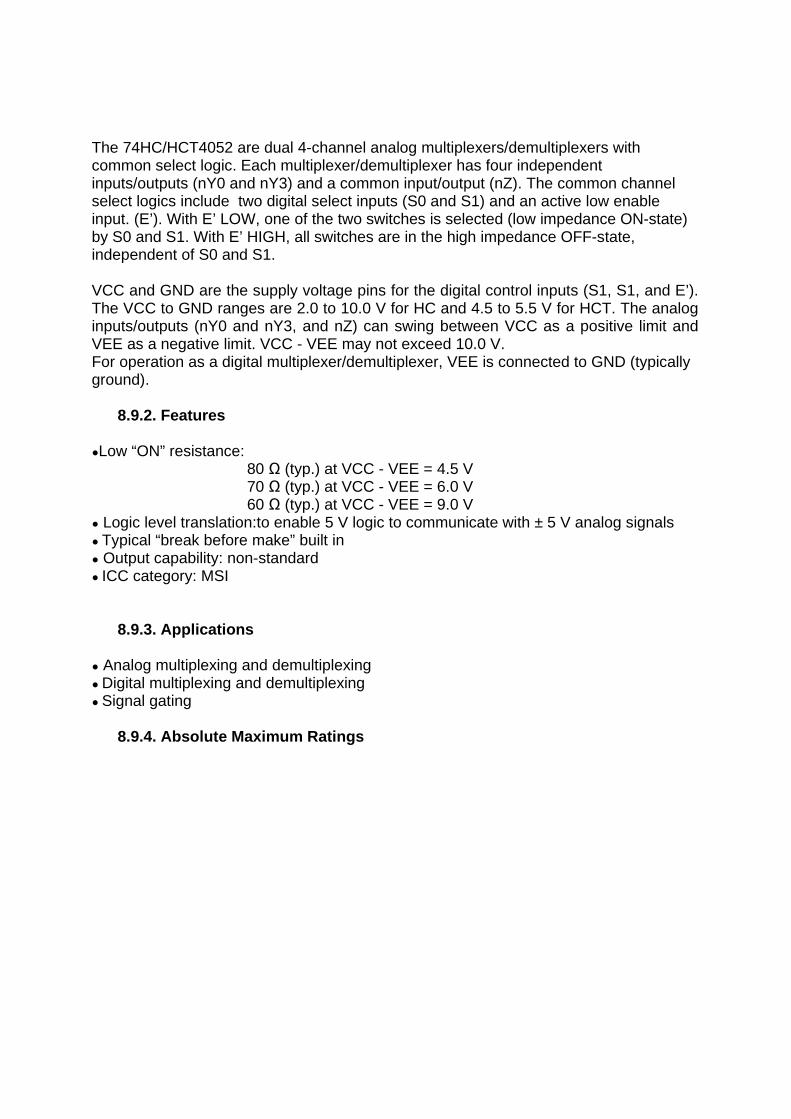
The 74HC/HCT4052 are dual 4-channel analog multiplexers/demultiplexers with common select logic. Each multiplexer/demultiplexer has four independent inputs/outputs (nY0 and nY3) and a common input/output (nZ). The common channel select logics include two digital select inputs (S0 and S1) and an active low enable input. (E’). With E’ LOW, one of the two switches is selected (low impedance ON-state) by S0 and S1. With E’ HIGH, all switches are in the high impedance OFF-state, independent of S0 and S1. VCC and GND are the supply voltage pins for the digital control inputs (S1, S1, and E’). The VCC to GND ranges are 2.0 to 10.0 V for HC and 4.5 to 5.5 V for HCT. The analog inputs/outputs (nY0 and nY3, and nZ) can swing between VCC as a positive limit and VEE as a negative limit. VCC - VEE may not exceed 10.0 V. For operation as a digital multiplexer/demultiplexer, VEE is connected to GND (typically ground). 8.9.2. Features Low “ON” resistance: 80 Ω (typ.) at VCC - VEE = 4.5 V 70 Ω (typ.) at VCC - VEE = 6.0 V 60 Ω (typ.) at VCC - VEE = 9.0 V Logic level translation:to enable 5 V logic to communicate with ± 5 V analog signals Typical “break before make” built in Output capability: non-standard ICC category: MSI 8.9.3. Applications Analog multiplexing and demultiplexing Digital multiplexing and demultiplexing Signal gating 8.9.4. Absolute Maximum Ratings
8.9.5. Pin Description
8.9.6. Function Table
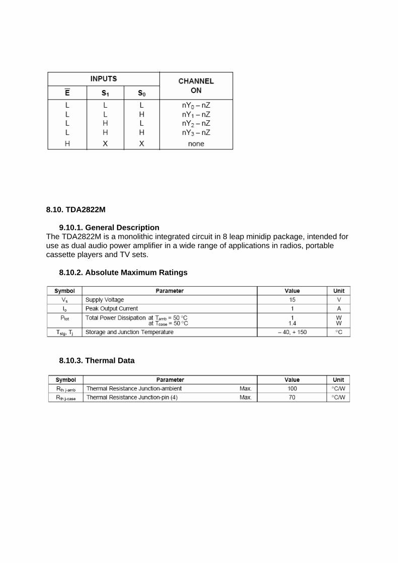
8.10. TDA2822M 9.10.1. General Description The TDA2822M is a monolithic integrated circuit in 8 leap minidip package, intended for use as dual audio power amplifier in a wide range of applications in radios, portable cassette players and TV sets. 8.10.2. Absolute Maximum Ratings
8.10.3. Thermal Data
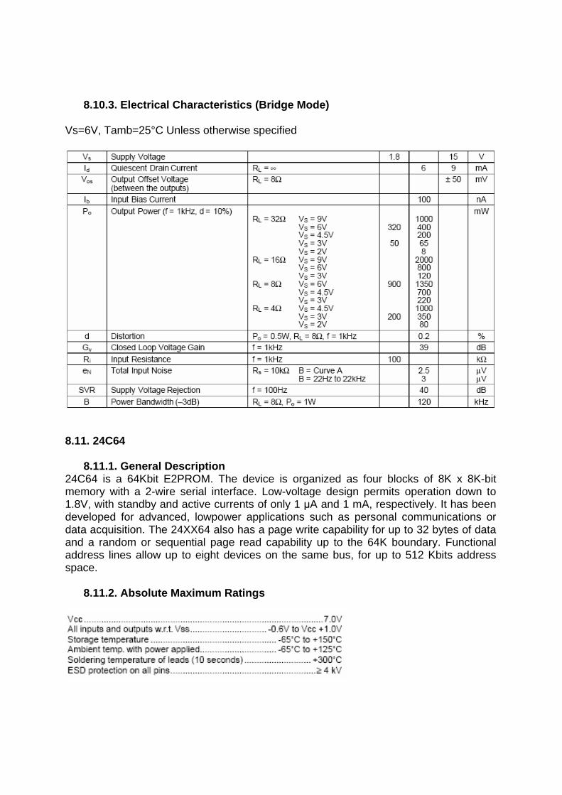
8.10.3. Electrical Characteristics (Bridge Mode) Vs=6V, Tamb=25°C Unless otherwise specified
8.11. 24C64 8.11.1. General Description 24C64 is a 64Kbit E2PROM. The device is organized as four blocks of 8K x 8K-bit memory with a 2-wire serial interface. Low-voltage design permits operation down to 1.8V, with standby and active currents of only 1 μA and 1 mA, respectively. It has been developed for advanced, lowpower applications such as personal communications or data acquisition. The 24XX64 also has a page write capability for up to 32 bytes of data and a random or sequential page read capability up to the 64K boundary. Functional address lines allow up to eight devices on the same bus, for up to 512 Kbits address space. 8.11.2. Absolute Maximum Ratings

8.11.3. Pin Connections
8.12. 24LC21 8.12.1. General Description 24LC21 is a 1Kbit E2PROM, organized by 8 bits. This device operates in two modes: Transmit Only mode and I2C bidirectional mode. When powered the device is initially in transmit only mode with E2PROM data clocked out during the rising edge of the signal applied on VCLK. The device switches to the I2C bidirectional mode upon the falling edge of the signal applied on SCL pin. The device can not switch from the I2C bidirectional mode to the Transmit only mode(except power off-on). The device can operate with a power supply value as low as +2.5V 8.12.2. Absolute Maximum Ratings
8.12.3. Pin Connections

9.OPEN-SHORT CIRCUIT PROTECTION In case of a component fault(open or short) there is a risk of exceeding the maksimum current rating for each of the power supply voltages. So a protection application is implemented in 17MB20. When the TV is ON if one of the ON Mode voltages (+8V, +5V, +3.3V and +12V) goes below the +2V threshold level the protection circuit pulls the PROTECT signal to low and the controller takes the chassy into Standby Mode. Since these voltages are only present in ON Mode, they are all switched off in the Standby Mode. Hence the risk of fire or component damage is prevented.
For the other voltages the above application cannot be implemented. So fuses are inserted serially in the required power supply lines in order to avoid component damage in case of a component failure. The fuse positions and ratings are given in the below table:
Voltage Rating Fuse
Position Voltage Label
Current Rating AC DC
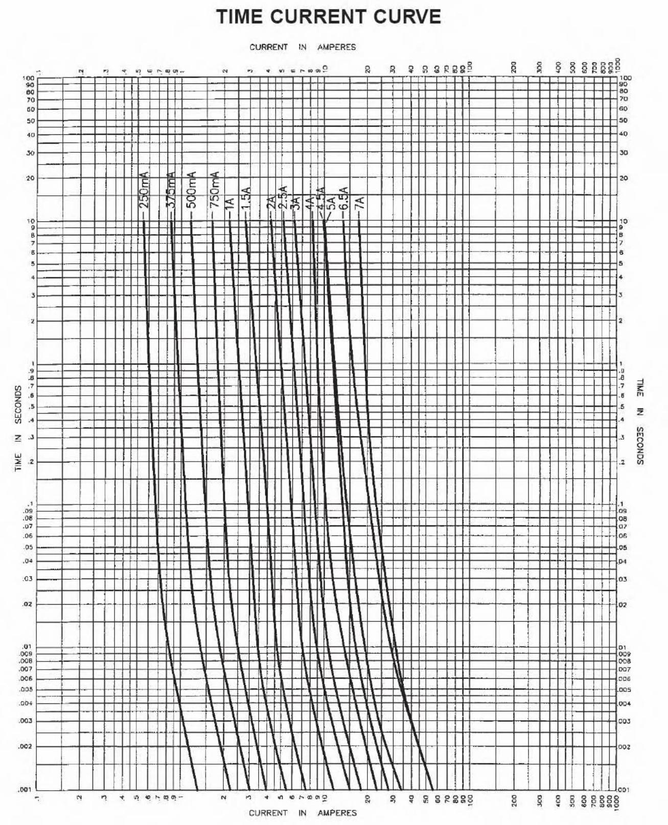
F600 +12V_INV 7A 32V 32V F601 +12V_PSU 5A 32V 32V F603 +3V3Stb 500mA 32V 63V F100 +12VStb 5A 32V 32V F102 +12V_AUD 1A 32V 63V In a possible case of fuse replacement, the inserted fuse must satisfy the above specifications. The fuses are subjected to inrush current for some time time interval, which may cause fuse interruption after service replacement. So, it is recommended to replace the fuses with the original part numbers. The current vs. time graph is given below.

10.SERVICE MENU SETTINGS Remote control code for openning the SERVICE MENU: MENU 4725 1. First APS <Yes/No> 2. BURN_IN_MODE <Yes/No> 3. FACTORY MENU
3.1.1. Language <English, Deutsch, Francais, Spanish, Portuguese, Italiano, Svenska, Dansk, Türkçe, Hungarian, Czech, Polish or Croatian>
3.1.2. Country <Germany, Denmark, Spain, France, Finland, UK, Greece, Hungary, Italy, Norway, Netherlands, Portugal, Poland, Swenden, Slovenia, Slovakia,Turkey, S.Afrika, Others, Japan, Korea, America, Austria, Belgium, Switzerland, Czech Rep.>
3.1.3. Volume <0..63> 3.1.4. Teletext Region < East Europe, West Europe, Cyrillic, Turkish/Greek, Arabic/Hebrew > 3.1.5. Menu Colour <Gray, Transparent> 3.1.6. PC Sharpness <0..31> 3.1.7. PC Colour <0..63> 3.1.8. Picture Mode
3.1.8.1.1.1. Brightness (Bright) <0..63> 3.1.8.1.1.2. Contrast (Bright) <0..63> 3.1.8.1.1.3. Colour (Bright) <0..63> 3.1.8.1.1.4. Sharpness (Bright) <0..31> 3.1.8.1.1.5. Brightness (Standard) <0..63> 3.1.8.1.1.6. Contrast (Standard) <0..63> 3.1.8.1.1.7. Colour (Standard) <0..63> 3.1.8.1.1.8. Sharpness (Standard) <0..31> 3.1.8.1.1.9. Brightness (Soft) <0..63> 3.1.8.1.1.10. Contrast (Soft) <0..63> 3.1.8.1.1.11. Colour (Soft) <0..63> 3.1.8.1.1.12. Sharpness (Soft) <0..31>
4. VCTI DAC Adjust.
4.1.1. Cutoff Red <0..511> 4.1.2. Cutoff Green <0..511> 4.1.3. Cutoff Blue <0..511> 4.1.4. Whitedrv. Red <0..511> 4.1.5. Whitedrv. Green <0..511> 4.1.6. Whitedrv. Blue <0..511> 4.1.7. PAL CVBS Brigh <0..63> 4.1.8. PAL RGB Brigh <0..63> 4.1.9. NTSC CVBS Brigh <0..63> 4.1.10.NTSC RGB Brigh <0..63> 4.1.11.PAL CVBS Color <0..63> 4.1.12.PAL RGB Color <0..63> 4.1.13.NTSC CVBS Color <0..63> 4.1.14.NTSC RGB Color <0..63>

5. Txt & FE OSD Settings 5.1.1. Txt&FE OSD H-Shift <0..255> 5.1.2. Txt&FE OSD V-Shift <0..255> 5.1.3. Txt H-Shift Split Screen <0..255> 5.1.4. Txt&FE OSD Pixel Clock <0..255> 5.1.5. YDELAY PAL <0..3> 5.1.6. YDELAY NTSC <0..3> 5.1.7. PKCOR (RF) <0..31>
6. Options1
6.1.1. IDTV <Yes, No> 6.1.2. SVHS-EXT2 <Yes, No> 6.1.3. FRONT-AV <Yes, No> 6.1.4. SVHS <Yes, No> 6.1.5. PC <Yes, No> 6.1.6. YPBPR <Yes, No> 6.1.7. BLUE SCREEN <Yes, No> 6.1.8. SEARCH FOR BG, DK, I <Yes, No> 6.1.9. SERAC FOR L/L’ <Yes, No> 6.1.10.Pref. Search Standard <BG-DK-I, L-L’, M> 6.1.11.Station Ident <Yes, No> 6.1.12.POWER ON TO STANDBY <Yes, No>
7. Options2 7.1.1. Tuner Options
7.1.1.1.1. Control Byte <128..256> 7.1.1.1.2. BSW1 <0..256> 7.1.1.1.3. BSW2 <0..256> 7.1.1.1.4. BSW3 <0..256> 7.1.1.1.5. VHF1-3-L <0..256> 7.1.1.1.6. VHF1-3-H <0..256> 7.1.1.1.7. VHF3-UHF_L <0..256> 7.1.1.1.8. VHF3-UHF_H <0..256> 7.1.1.1.9. Top Setting-PAL <0..15> 7.1.1.1.10. Top Setting-SECAM <0..15>
7.1.2. Blue Back. On Menu <Yes, No> 7.1.3. Dynamic Bass On Menu <Yes, No> 7.1.4. Vir. Dolby On Menu <Yes, No> 7.1.5. APS Delay Time(ms) <0..250> 7.1.6. Video Peaking <-8..15> 7.1.7. Comb Filter/CTI/LTI <Yes, No> 7.1.8. APS Test Mode <Yes, No>
8. Audio Options 8.1.1. Carrier Mute <Yes, No> 8.1.2. FM Presc_AVL_off <0..256> 8.1.3. NICAM Presc_AVL_off <0..256> 8.1.4. Scart Presc_AVL_off <0..256> 8.1.5. FM Presc_AVL_on <0..256> 8.1.6. NICAM Presc_AVL_on <0..256> 8.1.7. Scart Presc_AVL_on <0..256> 8.1.8. Line-out Via HP <Yes, No>

9. 9-Auto calibration 9.1.1. Exit 9.1.2. AutoColor 9.1.3. AdcGain
R 99 G 99 B 99 9.1.4. ADC Offset
R 133 G 129 B 145 9.1.5. Color temp Cool 9.1.6. Gain
R 140 G 140 B 140 9.1.7. Offset
R 118 G 120 B 127 9.1.8. Con Max 145 9.1.9. Bri Mid 104 9.1.10.Color 32 9.1.11.Sharp 9
10. 10-INIT NVM <Yes/No> 11. 11-SELECTED PANEL <SVA150XGA, M190A1, M190E5> Remote Control Type: RC1090, OTHERS, RC1243 SW Version 17MB20_STD_0.0.XX
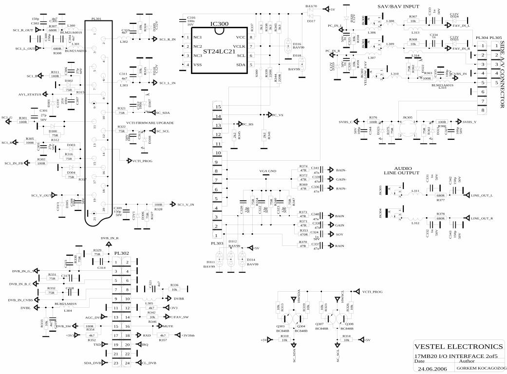
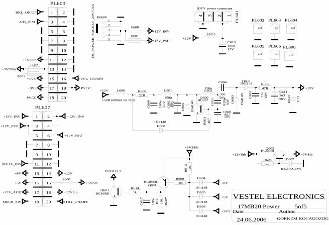
11. BLOCK DIAGRAMS AND SCHEMATICS 17MB20 Block diagrams and schematics are give in the following pages.

Adaptor DC INPUT
SCART
RGB,HS,VS
HW I2C
HW_RESET
LVDS CLK/DATA
RG
B,H
S,VS
/YP
bPr,
SOY
DDC I2C
TUNER
CS
I2C
TV_AGC
DVB_AGC
DVB_I2C
SW_AGC
SW_I2C
RY/G
B/C
RG
B, F
B
SC_L
/R_I
N
AV_
STA
TUS
SC_L
/R_O
UT
DVB_UART/HW_I2C
PRO
G_S
TATU
S
HW_I2C
UART2
UA
RT1
MA
IN Y
/C
SID
E Y/
C
BA
V_C
VBS
SAV_
CVB
S
SC_V
_OU
T
SC_V
_IN
LIN
E_L/
R_O
UT
SAV_
L/R
_IN
BA
V_L/
R_I
N
PC_L
/R_I
N
HP_
L/R
_OU
T
DVB
_L/R
_IN
SW_L/R_INPROG_STATUS
HP_
L/R
_OU
T
DVB_SW
DVB
_SW
SPK
_L/R
+
SPK
_L/R
-
SPK_L/R+
AV_STATUS
15" up to XGAPanel
+12V_PSU+12V_INV
+12V
+8V
+5V
+12V_AUD
+12V
+33V
+3V3
+3V3Stb
+1V8Stb
+1V8
+5VStb
+12VStb
+5VStb
PVCC
PVCC_ON/OFF
STBY_ON/OFF
MECH_SW
16R 16R
17PWI20Power
InterfaceBoard
SelfOscillatingRegulator
SeriesRegulator
SoftSwitch
PL40
0
TDA2822M2X2WRMS
74HC4052
VCT- I
DVBModule
TransistorSwitch
74HC4053
IF IFPL100
SAWFilter
TSU33AWL-LF
E2PROM24LC21
TransistorSwitch
PL30
0
MUTEPORT
BKL_ON/OFF
MUTEPORT
BKL_ON/OFF
MUTEPORT
PVCC_ON/OFF
BRT_ADJ
BRT_ADJ
BKL_ON/OFF
STBY_ON/OFF
I2CE2PROM24LC64
IF
IF
SAVModule
HP OUT(Detached)
BAV IN S-VIDEO IN LINE OUT
S-VIDEO INSAV IN
HP OUT(Detached)/ PC IN
VGA
PC_L/R_IN
PC_L
/R_I
N
IRQ
CVB
S
RGB, CVBS / Y, C Option
PVCC

1200mA +5V
1100mA +3V3
Max Current Voltage
Panel Logic Cct Requirements
400mA +1V8Stb
205mA +3V3Stb
30mA + 5VStb
30mA +12VStb
220mA +1V8
370mA +3V3
160mA +5V
12mA +8V
200mA+12V_AUD
5mA +33V
Max Current Voltage
Main Board Requirements
1200mA +5V
1100mA +3V3
Max Current Voltage
Panel Logic Cct Requirements
400mA +1V8Stb
205mA +3V3Stb
30mA + 5VStb
30mA +12VStb
220mA +1V8
370mA +3V3
160mA +5V
12mA +8V
200mA+12V_AUD
5mA +33V
Max Current Voltage
Main Board Requirements
Adaptor DC INPUT
+12V_PSUFUSE
FUSE +12V_INV
MECH_SW
MOSFETIRF7314 SO-8
STBY_ON/OFF
MPS15933A
SO-8
FDC642PSuper SOT
PVCC_ON/OFF
LM10861,5A
D2PAK
PVCC+3V3/+5V
+3V3Stb
Jumper Option
LM1117800mADPAK
STBY_ON/OFF
+1V8Stb
+1V8
+3V3
+5V/+3V3
SeriesRegulator
Jumper Option
+5VStb+12VStb
+12V_AUD
LM3171,5A
TO220
LM3171,5A
TO220
+8V
+5V
SelfOscillatingRegulator
+33V
+12V_IDTV
17PWI20
NTGS3446
NTGS3446
STBY_ON/OFF
MOSFETIRF7314 SO-8
Jumper Option

100nC176
100n
C151
+3V3Stb
+5V
220n
C164
1N4148
D102
100u
C127
10n
C168
1kR144
CVBS_IN
1kR145
100n
C145
SC1_OUT_L
100n
C148
20.2
5M
Hz
X100
10nC161
IF_CVBS_OUT
100u
C179
100n
C163
4k7R172
100n
C166
+3V3
100u
C133
VCT4932
IC102
1 GND1
3 VREFAU
5 SPEAKERR
7 AOUT1R
9 AIN3R/AOUT2R
11 AIN2R
13 SIF/AIN1R
15 VREFIF
17 IFIN+
19 GNDIF
21 VSUP3.3DIG
23 GND3
25 XTAL1
27 P22
29 VIN11
31 VIN9
2 VSUP8.0AU
4 SPEAKERL
6 AOUT1L
8 AIN3L/AOUT2L
10 AIN2L
12 AIN1L
14 TAGC
16 IFIN-
18 RESETQ
20 VSUP5.0IF 69XREF
71BOUT
73ROUT
75BIN
77RIN
79GNDM
81RSW1
83EW
85VERT+
87VSUP5.0BE
58SDA
60HOUT
62SAFETY
64VSUP3.3DAC
66GND6
68VSUP3.3BE
70VRD
72GOUT
74SVMOUT
76GIN
78FBIN
80SENSE
82RSW2
84VERT-
86TEST
88GND8
22 GND2
24 VSUP1.8DIG 65VSUP3.3IO
67GND7
26 XTAL2
28 P23
30 VIN10
32 VIN8
63GNDDAC
61HFLB
59VPROT
57SCL
33 VIN7
34 VIN6
35 VIN5
36 VIN4
37 VIN3
38 VIN2 51P14
52P15
53P16
54P17
55P20/DFVBL
56P21/PWMV
39 VIN1
40 VOUT1
41 VOUT2
42 VOUT3
43 VSUP1.8FE
44 GND4 45GND5
46VSUP3.3FE
47P10
48P11
49P12
50P13
25V
100u
C138
22pC150
100n
C152
SC1_V_IN
100n
C162
SC1_OUT_R
HWSDA
L112
100u
C178
100RR143
100n
C144
100u
C135
100RR152
3u3C134
100n
C155
100n
C143
100n
C154
100n
C167
LINE_L
100RR153
4k7R171
SW_OUT_L
100RR151
+8V
HWSCL
100n
C146
MAIN_R
+3V3
1n
C158
+1V8Stb22p
C149
100u
C140
100n
C139
+3V3Stb
100u
C136
+3V3Stb
100u
C177
LINE_R
SW_OUT_R
1k
R160
AGC_TV
100nC147
100n
C126
+5V
MAIN_L
L110BLM21A601S
100n
C142
L111
+3V3
+1V8Stb
100n
C153
4u7C182
1n
C165
IF2
IF1+8V
22u
C119
+8V
BC848BQ103
BC848B
Q101
1k
R102
+8V
22u
C105
1k
R114
22u
C106
SC1_OUT_L
SC1_OUT_R
SC1_L_OUT
1kR104
SC1_R_OUT
BC848BQ102
LINE_OUT_R
1k
R115
BC848BQ100
22u
C115
+8V
LINE_OUT_L
1n
C160
1n
C159
LINE_L
WP
+3V3Stb
100u
C113
100R
R110
24LC32A
IC100
1 A0
2 A1
3 A2
4 VSS 5SDA
6SCL
7WP
8VCC
100RR111
10n
C108
VCTI_HS
IRQ
100u
C132
16V
100n
C156
100n
C169
+3V3Stb
100n
C174
10kR175
100R
R186
100RR187
100RR135
100RR141
100RR142
470RR140
470RR138
470RR139
100R
R248
HWSCLHWSDA
100R
R246
100R
R238
TXDRXD
100R
R240
IR
MECH_SW
S113PL102
1
2
3
4
5
6
PL
10
3
1234
MECH_SW
LED2220RR158
S116
PL
10
4
1 2 3 4 5
KEY
L108
BLM21A601S
L106
L104
L105
L107
L109
BLM21A601S L117
BLM21A601S
L115
L116
BLM21A601S
L101
3k9
R128
10k
R134
4k7
R174
+3V3Stb
LED1
+3V3Stb4k7R163
22RR161
50V
22p
C175
22p C170
22RR162
270kR170
820k
R183
AV1_STATUS
100RR185 2k2
R190+3V3Stb
KEY
IR
15kR137
+3V3Stb
100RR150
R1784k7
TXD
4k7R179
CS
+3V3Stb 4k7R136
HWRESET
4k7R180
MUTE
100RR192
100RR191
SVHS_Y
SVHS_C
SDA
SCL
SC1_R
SC1_G
SC1_B
SC1_IN_FB10k
R176+3V3
BC848B
Q110
4k7R193
+3V3
200R
R199
100RR206
75R
R218
47RR212
47n
C194
BIN-
100RR208
47n
C191
47n
C190
75R
R227
200R
R205
47n
C193
BLUEO
75R
R229
100RR207
75R
R217
1RR201
BLUEO
BC858BQ120
+5VA
GREENO
BC858BQ116
47nC189
1RR200
REDO
200R
R196
BC858BQ115
47RR211
1RR202
BC858BQ119
47RR213
BC858BQ117
+5VA
GIN+
BC858BQ121
47n
C195
RIN+
75R
R228
+5VA
GREENO
RIN-
BIN+
REDO
GIN-
75R
R216
SDA
HWSCL
BC848B
Q106
CS
10k
R129
10k
R130
R12247k
R12747k
BC848B
Q105
SCL
R12447k
+3V3Stb
HWSDA
10kR131
10k
R133
BC848BQ108
BC848B
Q107
R12347k
SC
L_S
W
IF2
+5V
R116
100R
TV
/DV
B_S
WIT
CH
5k1
R121
10n
C123
1N
4148
D101
4k7
R107
R126
5k1
1uL100
5k1R125
S111
IF1R
105
100R
75R
R132
16V100u
C120
S108
10u
C124
22u
L102
PL1001
2
3
+33V
100u
C107
100n
C102
+5V
R119
100R
100n
C109
39pC118
1uC112
39pC114
TU
10
0TECH2949PG40B
AG
C1
TU
2
AS
3
SC
L4
SD
A5
NC
6
VS
7
NC
/AD
C8
VS
T9
IF2
10
IF1
11
AGC_SW
S101
SD
A_S
W
10nC122
3k3
R120
50V10n
C121
TV/DVB_SWITCH
SDA_DVB
AGC_TV
+5V
+3V3Stb
S102
S103
AGC_SW
S105
SCL
74HCT4053
IC101
1 2Y1
2 2Y0
3 3Y1
4 3Z
5 3Y0
6 E
7 VEE
8 GND 9S3
10S2
11S1
121Y0
131Y1
141Z
152Z
16VCC
SCL_SW
AGC_DVB
S104
SCL_DVB
S100
SDA
SDA_SW
100R
R117
100RR118
100n
C117
100n
C116
100R
R103
100n
C103
100R
R106
100n
C104
390R
R223
390R
R224
390R
R225
100u
C180
+3V3Stb
+3V3Stb
3k9R109
3k9R108
+3V3Stb
S109
S110
BC848BQ123
BC848BQ122
10kR244
10kR232
10kR239
10kR234
47kR233
47kR245
+3V3
+5V
+3V3
+5V
BLM21A601S
L113
WP
+3V3Stb
+5V
33k
R235
33kR168
POWCON
POWCON
STBY_ON/OFF
+3V3Stb
R165470R
470RR166
470RR167
100n
C171
100n
C172
100n
C173
50V
DVB_IN_B_C
DVB_IN_G_Y
DVB_IN_R
PROTECT
S124
2k7
R188
10k
R184
KEY
S118
S119
BZ
T55C
5V
1
D103
C5V
1
D104
+3V3
1u
C111
+3V3
10k
R100
10k
R113
1u
C101
10k
R112
1u
C110
1u
C100
+3V3
+3V3
10k
R101
+5VA
S106
PL101
1
2
3
4
5
DVB_IN_B_C
DVB_IN_G_Y
DVB_IN_CVBS
25V100n
C125
C5V
1
D100
BC848B
Q104
LINE_R
4k7 R169
100RR182
PC/FAV_SW
LED24k7
R164+3V3Stb
16V100n
C157
16V100n
C137
+3V3Stb
PL
10
5
1 2 3 4
16V100n
C141
BOUT
BOUT
GOUT
GOUT
ROUT
ROUT
+5VStb390RR155
4k7R159
+5VStb390RR148
BC848BQ109
1k
R173
LED1
+5VStb
M74HC4052
IC103
1 Y0
2 Y2
3 COM_Y_OUT_IN
4 Y3
5 Y1
6 INH
7 VEE
8 GND 9B
10A
11X3
12X0
13COM_X_OUT_IN
14X1
15X2
16VCC
DVB_SW
PC/FAV_SW
220n
C128
220n
C129
220n
C130
220n
C131
FAV_IN_R
FAV_IN_L
DVBL
DVBR
1kR147
1k
R146
SC1_R_IN
SC1_L_IN
SW_OUT_R
SW_OUT_L
100nC188
100nC199
+8V
S123
S122
S121
100kR242
100kR236
100n
C187
+8V
100kR220
+8V 100kR214
50V100n
C200
100kR243
50V100n
C201
+8V
100kR237
PC_IN_L
100kR215
100n
C186
100kR222
+8V
PC_IN_R
100kR247
+8V
100kR241
100n
C202
100kR209
+8V
100kR219
100n
C185
470R
R203
16V
100n
C184
820R
R204
BC858BQ118
SC1_V_OUT75RR221
27k
R197
IF_CVBS_OUT
50V
47p
C192
BC848BQ114
+8V
910RR210
10k
R198
47RR154
47R
R149
+3V3Stb
+3V3Stb
RXD
S125
BC848B
Q125
+3V3Stb
S126
10kR249
BC848BQ124
BF799Q126
BF799Q127
150RR250
150RR251
150R
R252
150R
R253
50V
1n
C203
50V
1n
C204
47k
R254
47k
R255
47k
R256
47k
R257
+5V
470R
R258
470R
R259
+5V
50V1n
C205
50V1n
C206
DIF1 DIF2 DIF2
DIF1
S127
S128
IF2
IF1
S129
S130S131
S132
390RR260
390R
R261
16V10u
C207
16V
10u
C208
S133
S134
33kR262
33kR263
10k
R264
10k
R265
S135
S136
S137
S138
FILTER_SAW_X6897DZ100
IN11
IN22GND
3
OUT1 4
OUT2 5
BLM21A601S
L114
+3V3Stb
1kR266
+3V3
BC848B
Q128
1k
R267
4k7R268
+5V
S139
+3V3Stb
ID-TV UYGULAMASINDA 2K LIK EEPROM TAKILACAK 30016178
FOR FLASH PROG.AND VCTI DEBUG
FOR MSTAR DEBUG
24.06.2006AuthorDate
17MB20 VCTI 1of5
GORKEM KOCAGOZOG
VESTEL ELECTRONICS
KEYPAD
GND_TUNER
PTC
IDT
V I
F C
ON
.
150p
C300
25V
100n
C307
4n7C310SC1_R_OUT
D302
150p
C302
4n7
C304
SC1_R
SC1_V_IN
C5V
1
D305
AV1_STATUS
D303
C5V
1
D306
L302
D300
L301
BLM21A601S
50V150pC309
50V
27p
C301
SC1_G
50V
27p
C303
SC1_IN_FB
SC1_B
680R
R308
4n7
C311
SC1_L_IN
SC1_R_IN
SC1_L_OUT
680RR307
150p
C308
50V
L303
C15V
D301
L300
BLM21A601S
4n7C305
D304
50V
27p
C306
SC1_V_OUT
A
JK303 1
23
A
JK304 1
23
LINE_OUT_L
LINE_OUT_R
PL301
1
2
3
4
5
6
7
8
9
10
11
12
13
14
15
16
17
18
19
20
21
PL303
1
2
3
4
5
6
7
8
9
10
11
12
13
14
15
BAV99
D311
BAV99
D312
BAV99
D314
+5V50V
12p
C320
50V
12p
C322
50V
12p
C323
220R
R344S300
+5V
BAV99
D318
PC_HS
ST24LC21
IC300
1 NC1
3 NC3 6SCL
8VCC
2 NC2
4 VSS
7VCLK
5SDA
PC_VS
3k3
R338
3k3
R34316V
100nC316
3k3
R337
BAV99D316
220R
R339
BAV70
D317
75R
R321
D308
A 1K 2
100n
C312
D307
A1K2
50V
100n
C313
SC_SDA
75R
R322
10k
R367
A
JK301 1
23
50V
1n
C333
A
YE
LL
OW
_F
AV
JK302 1
23
A
JK300 1
23
10k
R3681n
C334
FAV_IN_L
FAV_IN_R
100RR360
JK305
12
34
50V
100p
C344
75R
R375
SVHS_C
50V
100p
C327
100R
R376
SVHS_Y
75R
R361
D323
A 1K 2
D321
A 1K 2
10k
R325
10k
R324
100RR302
75R
R347
75R
R340
75R
R334
75RR315
75R
R312
75R
R316
75RR317
75R
R327
50V
1n
C331
L312
680R
R378
50V1n
C332
680R
R377
50V
150p
C343
50V
150p
C342
L311
100R
R328
100RR305
100RR301
100RR311
2k2
R341
2k2
R345
CVBS_IN
50V
100p
C335
100R
R363D322
A1K2
75R
R362
L308
L309
L310
BC848B
Q304
BC848B
Q303BC848B
Q307
BC848B
Q308
HW
SD
A
HW
SC
L
10k
R323
10k
R326
10k
R313
10k
R319
VCTI_PROGS
C_S
DA
SC
_S
CL
SC_SCL
+5V+5V 10kR314
10kR310
10k
R358
10k
R359
50V
1n
C325
50V
1n
C326
PC_IN_L
PC_IN_R
L306 L313
L314L307
C12V
D309
C12V
D310
C12V
D320
C12V
D319
C12VD324
C12VD325 PL304
1
2
3
4
5
6
7
8
PL305
1
2
3
4
5BLM21A601S
L315
PL302
1 2
3 4
5 6
7 8
9 10
11 12
13 14
15 16
17 18
19 20
21 22
23 24
75RR329
C314
DVB_IN_R
C315
DVB_IN_G_Y
75RR331
DVB_IN_B_C
C317
C318
DVB_IN_CVBS
75R
R332
DVBL
10k
R333
4n7
C319
L304
BLM21A601S
10k
R336
DVBR
4n7
C321
L305
AGC_DVB
+3V3
10k
R346
4k7
R342
PC/FAV_SW
4k7
R352
DVB_SW 100RR354
+3V3 4k7
R357
MUTE
RXD
TXD IRQ
SDA_DVB SCL_DVB
75R
R330
47RR373
47n
C340BAIN
50V1n
C324
47RR371
47n
C338GAIN
470RR353
SOY
RAIN47RR370
47n
C337
47RR374
BAIN-47n
C341
GAIN-47n
C33947R
R372
47n
C33647R
R369RAIN-
VCTI_PROG
+3V3Stb
VCTI FIRMWARE UPGRADE
SAV/BAV INPUT
17MB20 I/O INTERFACE 2of5
VESTEL ELECTRONICS
24.06.2006
Date Author
SID
E A
/V C
ON
NE
CT
OR
AUDIOLINE OUTPUT
GORKEM KOCAGOZOGL
VGA GND

A_TXOUT2+
A_TXOUT2-
PVCC
A_TXOUT3+
50V100nC447
A_TXOUT0-
25V100nC439
50V10n
C445
A_TXOUT3-
50V10n
C435
A_TXCLKOUT-
L407BLM21PG221SN1
A_TXCLKOUT+
A_TXOUT1+
S425
A_TXOUT1-
S426
A_TXOUT0+
L406
+3V3
S407
+3V3
S405
PWM2
+5V
BC848B
Q400
S404
C5V
1
D406
A1K2
+5V
16V
100n
C403
16V
100n
C400
16V
100n
C404
+3V3
VDDP
VDDC
L400
BLM21A601S
AVDD
L404
BLM21A601S
L401
BLM21A601S
+1V8
10u
C411
10u
C407
10u
C416
10u
C412
16V
47u
C417
50V
4u7
C427
C5V
1
D404
C5V
1
D400
C5V
1
D401
C5V
1
D405
100n
C419
100n
C420AV
DD
PC
_V
S
VC
TI_
HS
390R
R401
100n
C423
BIN
+
BIN
-
GIN
-
RIN
+
RIN
-
GIN
+
RA
IN-
BA
IN-
BA
IN
RA
IN
GA
IN
GA
IN-
SO
Y
100n
C430
100n
C431
S412 100n
C434
100n
C433
VDDP
100n
C429
100n
C426
VDDP
100n
C425
VDDCVDDP
100n
C418
22R
R417
3k9
R415
22R
R411
HWSCL
50V
39p
C442
HWSDA
CS
50V
39p
C441
50V
39p
C443
+3V3Stb3k9
R414
22RR416
+3V3Stb
4k7
R409
S413
+8V
S414
2k2
R413
BC848BQ404
470RR410
+3V3
16V100nC446
+5V
1kR420
4k7R412
4k7
R418
50V
4u7
C448
2k2
R419
PWM0
PWM0
22kR404 BC848B
Q403
10kR407
+3V3
10kR408
S411
100k
R405
BC848BQ402
50V
4u7
C432
10k
R406
PVCC_ON/OFF
100n
C428
PWM1
PWM1
100n
C438 VDDC
VDDP
100n
C437
100n
C436
100n
C408
VDDC
100n
C409
HWRESET
100R
R400
C401
14.3
1818M
Hz
X400
22pC402
100n
C410
AVDD
PC
_H
S
AV
DD AV
DD
VDDP
VD
DC
S409
S410 10k
R402
BC848B
Q401
S408
10k
R403
S415
S416
S417
S418
S419
S420
S421
S422
S423
S424
BKL_ON/OFF
A/D_DIM
A_T
XO
UT
3+
A_T
XO
UT
0-
A_T
XO
UT
3-
A_T
XO
UT
0+
A_T
XC
LK
OU
T+
A_T
XO
UT
1-
A_T
XC
LK
OU
T-
A_T
XO
UT
1+
A_T
XO
UT
2+
A_T
XO
UT
2-
PL403
1 2
3 4
5 6
7 8
9 10
11 12
13 14
15 16
17 18
19 20
TSU36AWL_M_LF
IC400
1N
C_
1
2G
ND
_1
3G
ND
_2
4R
EX
T
5A
VD
D_
1
6G
ND
_3
7A
VD
D_
2
8H
SY
NC
1
9V
SY
NC
1
10
BIN
1P
11
BIN
1M
12
SO
GIN
1
13
GIN
1P
14
GIN
1M
15
RIN
1P
16
RIN
1M
31DDC_CLK
32VDDP_1
33GND_5
34VDDC_0
35PWM0
36NC_2
37NC_3
38CS
39SCL
40SDA
41NC_4
42NC_5
43DDCROM_DAT
44DDCROM_CLK
45NC_6
46NC_7
65
LV
A0
M
66
VD
DC
_2
67
LV
B3
P
68
LV
B3
M
69
LV
BC
KP
70
LV
BC
KM
71
LV
B2
P
72
LV
B2
M
73
LV
B1
P
74
LV
B1
M
75
VD
DP
_5
76
GN
D_
9
77
LV
B0
P
78
LV
B0
M
79
GN
D_
10
80
BY
PA
SS
85 NC_8
86 PWM1_2
87 VDDP_6
88 NC_9
89 NC_10
90 NC_11
91 NC_12
92 NC_13
93 PWM0_2
94 NC_14
95 NC_15
96 XIN
97 XOUT
98 AVDD_?4
99 PWM2_2
100 NC_161
7B
IN0
M
18
BIN
0P
19
GIN
0M
20
GIN
0P
61
LV
A2
M
62
LV
A1
P
63
LV
A1
M
64
LV
A0
P
21
SO
GIN
0
22
RIN
0M
23
RIN
0P
24
AV
DD
_3
57
GN
D_
8
58
LV
AC
KP
59
LV
AC
KM
60
LV
P2
P
25
RE
FM
26
RE
FP
27
HS
YN
C0
28
VS
YN
C0
29
GN
D_
4
30
DD
C_
DA
T
47PWM2_1
48PWM1_1
49VDDP_2
50GND_6
51
VD
DC
_1
52
GN
D_
7
53
VD
DP
_3
54
LV
P3
P
55
LV
A3
M
56
VD
DP
_4
81 VCTRL
82 VDDC_3
83 GND_11
84 HWRESET
PL404
1 2
3 4
5 6
7 8
9 10
11 12
13 14
15 16
17 18
19 20
21 22
23 24
25 26
27 28
29 30
BC848B
Q405
4k7
R421
S427
+3V3
B_TXOUT2+
B_TXOUT0+
B_TXOUT2-
B_TXOUT0- B_TXOUT3+
B_TXOUT1-
B_TXCLKOUT-
B_TXOUT3-
B_TXCLKOUT+
B_TXOUT1+
S428
S429
S430
S431
S432S433
S434
S435
S436
S437
S438
AV
DD
100n
C440
VD
DP
PWM2
B_T
XO
UT
2+
B_T
XO
UT
2-
B_T
XC
LK
OU
T+
B_T
XO
UT
1-
B_T
XC
LK
OU
T-
B_T
XO
UT
1+
B_T
XO
UT
3+
B_T
XO
UT
3-
B_T
XO
UT
0-
B_T
XO
UT
0+
16V
100n
C449
100k
R422
22kR423
Date
VESTEL ELECTRONICS
24.06.2006
Author17MB20 SCALER 3of5
GORKEM KOCAGOZOGLU

PL501
1
2
PL500
1
2
MAIN_L
TDA2822M
IC501
1OUT1
2SUPPLY_VOLT
3OUT2
4GND5 IN21
6 IN22
7 IN11
8 IN12
25V100n
C508
25V
100n
C511
25V
100n
C510
4R
7R
506
4R7R504
4R
7R
507
TDA2822M
IC500
1OUT1
2SUPPLY_VOLT
3OUT2
4GND5 IN21
6 IN22
7 IN11
8 IN12
4R7R505
25V
100n
C509
25V100n
C515
25V
100n
C512
+12V_AUD
+12V_AUD
50V
10n
C507
50V
10n
C506
50V
10u
C504
50V
10u
C502
25V
10n
C505
25V
10n
C503
1k
R503
1k
R502
3k3R501
3k3R500
63V680n
C501
63V680n
C500
PH
JAC
KJK
500
1
2
3
4
5
6
7
8
9
MAIN_R
C12VD505
PC
_IN
_L
PC
_IN
_R
10kR511
BL
M21A
601S
L504
50V4n7
C518
10k
R510
C12VD503
50V4n7
C519
BL
M21A
601S
L505
HP_L
HP_L
HP_R
HP_R
RIGHT+ LEFT+
RIGHT+
LEFT+
LEFT-
LEFT-
RIGHT-
RIGHT-
LEFT+
RIGHT+
C12V
D504 A1
K2
C12V
D501
A 1K 2
L503
L500
C12V
D500
A 1K 2
L501
C12V
D502
A 1K 2
L502
PL502
1
2
3
4
5
S501
S500
LEFT+
RIGHT+
50V
47u
C513
50V
47u
C514
50V1u
C516
50V1u
C517
220RR508
220RR509
MUTE1kR512
4k7R513
10k
R514
1kR516
BC848BQ500
BC848BQ501
BC
858B
Q502
1N
4148
D506
16V
470u
C520
+3V3Stb
+12VStb
10k
R515
MUTE_INV
16V
10u
C521
24.06.2006
AuthorDate17MB20 AUDIO 4of5
Gorkem Kocagozoglu
VESTEL ELECTRONICS
4-5/7-8: Unplugged5-6/8-9: Plugged
LE
FT
SP
KR
IGH
T S
PK
F601
+12V_INV
DC
_P
OW
ER
_S
OC
KE
T_20V
/7.5
A
JK6001
2
3
4
5
F600
+12V_PSU
1N4148D602
150u
L601
50V4n7
C606
47RR605
+12V
22RR600
50V
820p
C605150R 600mA lik ferit
L600
50V33n
C604
4k7
R601
1N
4148
D603
50V
4n7
C601
25V
100n
C600
50V
33n
C609
1N4148
D600
150uL602
+33V
50V3u3C611
BC337Q600
1N
4148
D601
PL
60
1
1234
10k
R607
+12V
35V100uC613
PROTECT
L603
16V
100n
C617
1N4148
D60510k
R613
+8V
1N4148
D606
+3V3
10kR609
BC858BQ601
+5V
1N4148
D604
+3V3StbBC548B
Q602
6k8R608
+5VStb+12VStb
BZX79C5V6
D607
C33
D608
PL603
1
PL604
1
PL605
1
PL606
1
PL602
1
PL600
1 2
3 4
5 6
7 8
9 10
11 12
13 14
15 16
17 18
19 20
PVCC_ON/OFF
PL607
1 2
3 4
5 6
7 8
9 10
11 12
13 14
15 16
17 18
19 20
BKL_ON/OFF
A/D_DIM
+1V8Stb
+3V3Stb
+1V8
+3V3
PVCC
PVCC
+12V_INV
+12V_PSU
+12V_INV
+12V_PSU
+12VStb
STBY_ON/OFF
+5V
+12V_AUD
MECH_SW
+8V +12V
S600+5VStb
PL608
1
BC848BQ603
1kR614
F602
MUTE_INV
F603
Date
VESTEL ELECTRONICS
24.06.2006
Author17MB20 Power 5of5
GORKEM KOCAGOZOGL
IDTV power connector

50V100n
C125
50V100nC140
1k
R117
HER206
D100
BC848BQ105
10RR125
10kR127
+12VStb
16V100uC141
22k
R120
+12VStb
100n
C127
+12V_AUD
+12V
10RR129
22kR130
BC848B
Q103
IRF7314
IC101
1 S1
3 S2 6D2A
8D1A
2 G1
4 G2
7D1
5D2
22k
R124
+3V3Stb
LM1086IC105
1GND
2VOUT3 VIN
16V100nC107
220R
R105
1RR107
16V
100n
C105 390R
R106
+5V/+3V3Stb
16V220uC118
50V
22u
C111
16V100nC115
16V100nC101
S100
SS
33
IC12
50V100nC119
30k
R122
50V100nC106
+12VStb
+5V/+3V3Stb
150R 600mA lik ferit
L101
150R 600mA lik ferit
L100
2k
R121
16V220uC138
16V
22u
C129
50V10n
C133
16V
22u
C132
50V
100n
C130
16V220uC112
10u
L102
50V22n
C123
50V
100n
C137
50V100nC100
1k
R128
22uH_3.9A_SMD
L103
50V
10u
C114
50V
10u
C117 MP1593-DC/DC
IC102
1 BS
3 SW 6COMP
8SS
2 IN
4 GND
7EN
5FB
50V10n
C134
10kR126
7k5
R131
+1V8Stb
LM1117-DPAK-1.8VIC106
4
VOUT2OUT
1
GND3 IN
16V100nC108
+3V3Stb
16V100uC116
16V100nC113
PVCC
16V10u
C109BC848B
Q100
PVCC_ON/OFF FDC642PQ101
1234 5 6
22kR103
22k
R104
+5V/+3V3Stb
10kR101
100n
C110
+12V_PSU
50V
100n
C102
220u
C120
16V50V100nC122
MECH_SW
50V100nC104
+12VStb
22k
R102
22kR100
IRF7314
IC100
1 S1
3 S2 6D2A
8D1A
2 G1
4 G2
7D1
5D2 MUTE_INV
STBY_ON/OFF
16V100uC143
+12V_INV
50V100nC142
BKL_ON/OFF
A/D_DIM
+12V_PSU
+12V_INV
+5V/+3V3Stb
+12V_PSU
+5V
+12V_INV
+12VStb
+12V_AUD
STBY_ON/OFF
MECH_SW
PVCC_ON/OFF
PVCC PVCC
+3V3
+1V8
+3V3Stb
+1V8Stb
A/D_DIM
BKL_ON/OFF
PL101
1 2
3 4
5 6
7 8
9 10
11 12
13 14
15 16
17 18
19 20
PL100
1 2
3 4
5 6
7 8
9 10
11 12
13 14
15 16
17 18
19 20
S101
100RR114
50V
68n
C124
STBY_ON/OFF
NTGS3446
IC103
1 D1
3 G 4S
6D4
2 D2 5D3
+1V8Stb
12k
R110
BC848B
Q102
+1V8
16V
47u
C128
16V
100u
C136
3k3
R112
4k7
R111
+12VStb
3k3
R113
16V
47u
C131
3k3
R119
+3V3Stb
BC848BQ104
12k
R115
50V
68n
C126
+12VStb
16V
100u
C139
100RR123
3k3
R118
+3V3
NTGS3446
IC104
1 D1
3 G 4S
6D4
2 D2 5D3
1kR116
PL102
1
2
3
4
5
6
7
8
9
10
11
16V
100n
C144
16V
100n
C145
+8V
+12V
MUTE_INV
BC848B
Q106
+3V3Stb
10RR134
10RR135
HER206
D101
LM317IC107
1ADJ
2OUT3 IN
LM317IC108
1ADJ
2OUT3 IN
35V
100u
C146
16V
100u
C147
35V
100u
C148
16V
47u
C149
16V
47u
C150
16V
100n
C151
16V
100n
C152
16V
100n
C153
16V
100n
C154
+12V
16V
100n
C155
16V
100n
C156
91R
R136
470R
R137
47R
R138
220R
R139
680R
R140
1R
R141
+8V +8V +5VS
TB
Y_O
N/O
FF
_IN
V
STBY_ON/OFF_INV
+1V8
+3V3Stb
F100
F101
F102
50V
100n
C157
OPTIONAL JUMPER
R120 will be 15k ohm for 3.3V output.
C134 will be 8.2 nF for 3.3V output.
Optional NC
Optional NC
R130 will be 5.6k ohm for 3.3V output.
Tact Switch Option
24.06.2006 Gorkem Kocagozoglu Date17PWI20-1
VESTEL ELECTRONICS

˜G$
1"
2"
23"
24"
1"
1"
2"
88"
25" 43"
44" 1"
45"
46" 64"
20"
69" 87"
3" 4"
2" 1"
5"
1"
E "
B "
C "
E "
B "
C "
UA"
17MB20-1" 110706"
C107"
C11
3"
C120"
C124"
C127"
C132" C133"
C134"
C136"
C138"
C14
0"
C177"
C178"
C179"
C180"
J157
"
C182"
J155
"
C521"
C520"
PL302"
R37
2"
PL404" C407" C411"
C412"
C416"
C417" PL403"
PL600"
PL607"
C427"
C432"
C448"
C513"
C51
4"
R206"
C611"
C613"
J182
" J1
51"
J173
"
J179
"
IC50
0"
IC50
1"
IC10
0"
IC10
2"
JK300"
JK30
1"
JK302"
JK30
3"
JK30
4"
JK30
5"
JK50
0"
JK60
0"
PL100"
PL101" PL102"
PL104"
PL105"
PL301"
R207"
PL30
3"
PL30
4"
PL30
5"
R208"
R37
4"
PL50
2"
PL60
1"
J137
" J1
36"
J167
"
J130"
Q60
0"
PL60
2"
R14
5"
PL603"
PL604"
PL605"
PL60
6"
R37
3"
R211"
C10
0"
C101"
C105"
C10
6"
C11
0"
C111"
C11
5"
C119"
C13
5"
R400"
J125
"
J107"
C500" C501"
C502"
C504"
C516"
C517"
R212"
D607"
Z100"
L100
"
R213"
L601
"
L602
"
PL103"
PL500" PL501"
J201"
Q60
2"
R10
0"
R10
1"
R10
5"
R110"
R111"
R11
2"
R11
3"
D10
2"
R11
8"
R13
4"
R13
5"
R10
3"
R14
1"
R14
2"
R14
4"
J112"
J120
"
R10
6"
R11
7"
R15
3"
R15
8"
R15
9"
R16
1"
R16
8"
R18
3"
R18
5"
R18
6"
R18
7"
S113
"
R19
0"
R19
1"
R250"
R251"
R200"
R201"
R202"
S600
"
J150
"
J127
"
R22
1"
J132
"
R30
1"
R15
0"
J135
"
R30
5"
J134
"
R31
1"
R512"
R32
1"
R32
8"
R15
2"
J199"
J202
"
R13
8"
J122
"
R13
9"
R14
0"
R36
0"
R36
3"
J121
"
J119
"
J148
"
R37
6"
J147
"
J238
"
S104"
J223
"
J104
"
J100
"
J222"
S405"
S409"
S413"
S414"
J158
"
PL60
8"
TU100"
X100
"
X400"
J166
"
J163
"
J240
"
J162
"
J220
"
J165
" J1
15"
J114
"
J113
"
J169
"
J168
"
J153
"
J152
"
J219
"
R32
2"
J224
"
J241
"
J205
"
J197
"
R35
7"
R35
4"
J233"
J231" J228"
J226"
J225"
J117
"
J203
"
J186
" J1
87"
J188
"
J206"
J133
"
J131
"
J146
"
J235"
J211"
J232
" J234"
J217
"
J214" J213"
J221
"
J189
"
J184
"
J209"
J129
"
J128
"
J118
"
J123
"
J139
"
J239"
J204
"
J215"
J212"
J208"
J200
"
J236
"
J237
"
J178
"
J177
"
J161
"
J164
" J160
"
J170"
J109" J106"
J159
"
J145
"
J124"
J126"
J154"
J171"
J181"
J102"
J101"
J180"
J183"
J192"
J156
"
J190"
J138
"
J149
"
J175
" J1
74"
J176
"
J191"
J227
"
J230"
J143
"
J193"
J141"
J110
" J1
11"
J142
"
J195"
J185
"
J198"
J196"
J172
"
J140
"
J229"
J216
"
J103
"
J116
"
J144"
J105"
J242"
R27
2"
J108"
J207"
J194"
J210
"

PG$
C10
2"
C103"
C104"
C107"
C10
8"
C109"
C112"
C11
3"
C114" C116"
C11
7"
C118"
C120"
C121"
C122"
C123"
C12
4"
C127"
C132" C133"
C134"
C136"
C13
7"
C13
8"
C13
9"
C14
0"
C14
1"
C14
2"
C143"
C14
7"
C14
8"
C14
9"
C15
0"
C15
6"
C15
7"
C15
8"
C15
9"
C16
0"
C16
1"
C16
2"
C16
3"
C16
4"
C16
5" C
166"
C16
7"
C16
8"
C16
9"
C20
7"
C17
4"
C175"
C17
6"
C17
7"
C178"
C179"
C18
0"
J157
"
C182"
J155
"
C184"
C18
8"
C192"
C521"
C44
9"
C520"
C199"
C30
0"
C301"
C30
2"
C30
3"
C304" C305"
C306"
C30
7"
C30
8"
C30
9"
C31
0"
C31
1"
C31
2" C313"
C314"
C317"
C316"
C315"
C318"
C319" C
321"
C32
5"
C326"
C327"
PL302"
R36
9"
R37
2"
C331"
C33
2"
C333"
C334"
C33
5"
C34
2"
C34
3"
C344"
C40
0"
C401"
C40
2"
C403" C40
4"
IC400"
PL404"
C407"
C408"
C40
9"
C41
0"
C41
1"
C41
2"
Q12
8"
Q40
5"
Q50
0"
C41
6"
C41
7"
C41
8"
C419"
C42
0"
PL403"
PL600"
C42
3"
PL607"
C42
5"
C426"
C427"
C42
8"
C42
9"
C43
0"
C208"
C432"
C43
4"
C43
5"
C436"
C43
7"
C438"
C43
9"
C44
0"
C441"
C442"
C443"
Q124"
C44
5"
C44
6"
C44
7"
C448"
C50
3"
C505"
C506"
C507"
C50
8"
C509"
C51
0" C
511"
C51
2"
C513"
C51
4"
C515"
C51
8"
C51
9"
Q50
1"
Q60
3"
C600"
C60
1"
R254"
R257"
C60
6"
R255"
R256"
C60
9"
R206"
C611"
R258"
C613"
R259"
J182
"
J151"
C617"
J173
"
J179
"
R514"
D10
0"
D10
3"
D104"
D300" D302" D303"
D304" D305" D306"
D32
1"
D32
2"
D32
3"
D40
0"
D40
1"
D311"
D31
2"
R515"
D314"
R42
2"
D31
6"
D31
8"
S13
3"
S13
4"
D404" D40
5"
D40
6"
D30
1"
D30
7"
D308"
D309"
D31
0"
D319"
D32
0"
D324"
D325"
D500"
D50
1"
D50
2"
D50
3"
D50
4"
D50
5"
D601"
D60
3"
D101"
IC300"
IC500"
IC501"
S438"
IC100"
IC10
1"
IC102"
IC10
3"
S127"
JK300" JK301" JK302" JK303" JK304" JK305"
JK500"
JK600"
PL1
00"
PL101" PL102"
PL1
04"
PL105"
S12
8"
PL301"
R207"
PL303"
PL304"
PL305"
R208"
R37
4"
PL502"
S41
5"
R24
6"
PL6
01"
Q108"
S12
9"
S13
0"
S13
1"
S13
2"
J137
"
J136
"
Q400"
Q40
1"
Q40
2"
Q40
3"
Q40
4"
J167
"
J130"
S13
9"
Q60
0"
R10
2"
R104"
R114"
R11
5"
PL602"
R132"
R16
0"
R17
0"
R173"
R17
5"
S42
7"
R196"
R198"
R199"
R204"
R20
5"
R24
8"
S42
8"
D602"
R219" R220"
R22
2"
S42
9"
S43
0"
S43
1"
R235"
R236"
R23
7"
R24
1"
R14
5"
R315" R316"
R317"
R32
4"
R32
5"
R327"
PL603"
PL604"
PL605"
PL606"
S43
2"
R12
8"
R34
1"
R34
5"
R37
0" R
371"
R
373"
R35
8"
R359"
R36
1"
R36
2"
C32
4"
C33
6"
C33
7"
R367"
R36
8"
C33
8"
C33
9"
C34
0"
R375"
R40
5"
R41
2"
R413"
R50
2"
R503"
R51
0"
R51
1"
S43
3"
R60
7"
S43
4"
S10
1"
S106"
S108"
S43
5"
S12
3"
S43
6"
R211"
S40
4"
S41
2"
S426"
S43
7"
C10
0"
C10
1"
C105"
C10
6"
C110"
C11
1"
C115"
C11
9"
C12
5"
C126"
C128"
C12
9"
C130" C131"
C13
5"
C144"
C14
5"
C14
6"
C151"
C152"
C15
3"
C154"
C15
5"
C17
1"
C17
2"
C17
3"
C18
5"
C18
6" C187"
C189"
C190" C191"
C193" C194" C195"
C20
0"
C20
1"
C20
2"
C32
0" C
322"
C323"
C34
1"
R146" R14
7"
R35
3"
R40
0"
J125"
J107"
C433"
C50
0"
C50
1"
C502"
C50
4"
C51
6"
C51
7"
C604"
C605"
D60
0"
R329"
D31
7"
R212"
D604"
D60
5"
D60
6"
D607"
D60
8"
R312"
F600
"
F601
"
Z100
"
C20
3"
L100"
L101
"
L102"
L104
"
L105
" L106"
L107"
L108"
R330"
L110
"
L111
"
R331"
L113
"
C20
4"
L115
"
L116
"
L117
"
L300
" L3
01"
L302
"
L303"
R332"
R333"
L306
"
L307
"
L308
"
L309
"
L310
"
L311"
L312"
L313
"
L314
"
L400"
L401"
C205"
C20
6"
L404"
R213"
L406
"
L407
"
L500"
L501
"
L502
"
L503"
L504
"
L505
"
L600" L601"
L602
"
L603"
PL1
03"
PL500"
PL5
01"
Q100" Q101"
Q102"
Q10
3"
Q104"
Q105" Q106"
Q10
7"
Q109" Q110"
Q114"
Q115"
Q116"
Q117"
Q118"
Q119"
Q120"
Q121" Q122"
Q12
3"
R33
6"
D50
6"
J201"
Q303"
Q304"
Q30
7"
Q30
8"
Q60
1"
Q60
2"
R10
0"
R10
1"
R17
6"
R10
5"
R34
6"
F603"
R10
8"
R10
9"
R110"
R111"
R11
2"
R11
3"
D10
2"
L109
"
R11
8"
R119"
L305"
R121"
R12
2"
R123" R124"
R125"
R12
6"
R127"
R12
9"
R13
0"
R13
1"
R133"
R13
4"
R13
5"
R13
6"
R13
7"
L112
"
L304"
R10
3"
R141" R142"
R143"
R14
4"
L114
"
J112"
J120
" R
148"
R14
9"
R10
6"
R151"
R11
7"
R15
3"
R15
4"
R15
5"
Q126"
Q12
7"
R158"
R15
9"
R16
1"
R162"
R16
3"
R16
4"
R16
5"
R16
6"
R16
7"
R16
8"
R16
9"
R17
1"
R17
2"
R17
4"
R116"
Q50
2"
R17
8"
R17
9"
R18
0"
C43
1"
R18
3"
R18
4"
R18
5"
R18
6"
R18
7"
R18
8"
S11
3"
R19
0"
R19
1"
R192"
R19
3"
R250"
R251"
R197"
R200"
R201"
R202"
R203"
R20
9"
R21
0"
S60
0"
J150
"
J127
" R21
4"
R21
5"
R21
6"
R21
7"
R21
8"
R22
1"
R223"
R224"
R225"
R227"
R228"
R229"
R232"
R233"
R23
4"
R238"
R239" R240"
R242"
R243"
R244"
R245"
J132
"
R247"
J288"
R25
2"
R30
1"
R15
0"
R253"
J135
"
R30
5"
J134
"
R30
7"
R30
8"
R26
6"
R31
0"
R31
1"
R313"
R31
4"
R26
7"
R31
9"
R512"
R321"
L315
"
R32
3"
R326"
R328"
R334"
J296
"
R337"
R338"
R339"
R34
0"
R15
2"
R343"
R34
4"
R30
2"
R34
7"
J199"
R120"
J202
"
R13
8"
J122
"
R13
9"
R14
0"
R36
0"
R36
3"
J121
"
J119
"
J148
"
R37
6"
R377" R378"
J147
"
R401"
R402"
R40
3"
R40
4"
R40
6"
R407"
R40
8"
R409"
R41
0"
R411"
R414"
R415"
R416" R417"
R418"
R419" R42
0"
R500"
R50
1"
R50
4"
R505"
R50
6"
R507"
Q125"
R107"
R516"
R26
8"
R42
1"
R600"
R60
1"
R51
3"
R42
3"
R605"
R61
4"
R60
8"
R609"
J238
"
J295
"
R613"
S100"
S10
2"
S10
3"
S104" S105"
R24
9"
S10
9"
S11
0"
S11
1"
R50
8"
J223
"
J104
"
J100"
S11
6"
S11
8"
S11
9"
S121"
S12
2"
S12
4"
S300"
R50
9"
J298"
J222"
S405"
S407"
S40
8"
S409"
F602
"
S41
1"
S413"
S414"
S41
6"
S41
7"
S41
8"
S41
9"
S42
0"
S42
1"
S42
2"
S423"
S424"
J158
"
S425"
S50
0"
S50
1"
PL608"
TU100"
X10
0"
X40
0"
J166
"
J163
"
J240
"
J162
"
J220
"
J165
"
J115
"
J114"
J113
"
J169
"
J168
"
J153
"
J152
"
J219
"
R32
2"
R34
2"
J290"
J224
"
J241
"
S125"
S126"
J205
"
J197
"
R35
2"
R35
7"
R35
4"
J233"
J231"
J228"
J226"
J225"
J117
"
J203
"
J186
"
J187
" J1
88"
J206"
J133
"
J131
"
J146
"
J284"
J289
"
J235"
J211"
J232
"
J300
"
J234"
J217
"
J214"
J213"
J283
"
J221
"
J301
"
J189
"
J184
"
J209" J1
29" J1
28"
J118
"
J123
"
J139"
J285
"
J274"
J239"
J204
"
J215"
J212"
J208"
J200
"
J299"
J294"
J292
"
J291"
J236
" J237
"
J297
" J1
78"
J177
"
J161
"
J164
"
J160
"
J170"
J109
" J1
06"
J159
"
J145"
J124" J126"
J154"
J171"
J181"
J102"
J101"
J180"
J183"
J192"
J156
"
J286
"
J190"
J138
"
J149
"
J175
"
J174
"
J176
"
J191"
J302"
J227
"
J230"
J143
"
J193"
J141"
J110
"
J111
"
J142
"
J195"
J185"
J198"
J278
" J196
"
J172"
J140
"
J279"
J229
"
J216
"
J103
"
J116
"
J144"
J275"
J105"
J242"
J276"
J277"
R182"
R26
9"
R270"
R271"
R27
2"
R37
9"
S410"
J108"
J273"
J272
"
J270"
J207" J282"
J281"
J280"
J194"
J293
"
J210
"
J271
"

ÀH$
1"
1"
1"
1"
M" M" AS"
280706" 17PWI20-2"
C112" C118"
C10
4"
C10
7"
C108"
C10
9"
C111" C
120"
C114"
C11
5"
C11
3"
C117"
C116"
C138"
C12
8"
C13
1"
C129"
C13
2"
C136"
C146"
C139"
R116"
C141"
C126"
C14
3"
IC12
"
IC10
2"
IC10
6"
PL10
1"
PL100"
IC10
3"
Q103"
IC10
4"
Q10
5"
R12
6"
C147"
C11
0"
C123"
C14
8"
IC105" R118"
R119"
R123"
L102
" L1
03" PL
102"
C14
9"
C150"
Q101"
R10
4"
R105"
C15
5"
R138" R117"
R121"
R12
2"
R12
7"
R13
0"
D100" D101"
F102
"
IC107"
IC108" R13
4"
R13
5"
R13
7"
S100"
S101"

¸D$
C10
0"
C10
1"
C112"
C157"
C118"
C105"
C106"
C109"
C111"
C120"
C116"
C138"
C119"
C128"
C14
4"
C122"
C131"
C125"
C13
0"
C136"
C134"
C14
6"
C139"
Q102"
Q104"
C137"
R11
1"
C140"
C124"
C141"
C14
2"
C143"
IC10
2"
PL101"
PL100"
C14
5"
Q100"
R107"
R12
8"
R110"
R131"
C14
7"
C102"
R115"
C127"
C133"
R112"
C14
8"
IC10
0"
IC10
1"
R113"
L100
"
L101
"
R114"
PL1
02"
C14
9"
C15
0"
R100"
R101"
R102"
R10
3"
R106"
C15
1"
C15
2"
C15
3" C
154"
C15
6"
Q106"
R14
1" R12
0"
R124"
R125"
R129"
D100"
D101"
F100
"
F101"
R13
6"
R139" R14
0"
S100"
S101"

NO LEVEL CODE NAME QUANTITY POSITION1 1 20181872 SNOW BOX ASSY TFT(F/B) 1510/11 12 2 20166591 SNOW BOX FRONT LCD 1510/11 14 2 20166683 SNOW BOX BACK LCD 1510/11 1
21 2 20188267 BUTTON FUNC.TFT XX10-11 (SILVER/P) 122 3 20174894 BUTTON FUNC.TFT XX10-11 (EKO.GRAY/I) 125 2 20188268 BUT.ON/OFF TFT XX10-11 (SILVER/P)(SM BAS 126 3 20174895 BUT.ON/OFF TFT XX10/11 (EKO.GRAY)(SM BAS 131 2 20188269 FOOT ASSY 1510/11 (SILVER/P) 137 3 35000180 SCREW C ZN YSMB M3*6 ROHS 538 3 35004316 SCREW P C ZN YSMB 3*6.5 RoHS 541 3 45004526 HINGE TFT 1510-11 ROHS 145 2 35015033 SCREW C ZN YSMB M3x12 (ST) ROHS 446 1 20264518 POWER CORD ASSY.SAFE(EUR.WAL PLG)-PKG 147 2 30002376 POWER CORDSAFE MON.(EUR.WAL PLG)PKG RoHS 149 1 20278423 BRACKET CHS.MB20(VER 4)15"EKO.GRAY(I) 151 2 20188317 MD.ASY.17LD12-LED BOARD 1510/11(ROHS 153 4 30010688 LED RED/GREEN VDC30354 3MM RoHS 1 D1054 4 30031033 PREAMPLIFIER TFMS5360 RoHS 1 IC1055 4 30037373 CNAS 5P-6/560 FLT W/C UL2468AWG24 RoHS 1 PL261 7 30000459 RES CF 1/4W 100R J. ROHS 1 R163 5 30000371 CAP EL 22UF 50V M ROHS 1 C1064 2 20262601 MD.ASY.17TK36-6SW 2010/11TFT (MB24)(ROHS 167 4 30027440 PUSH SWITCH ON/OFF 0.1A/12RoHS 1 SW668 4 30032684 SWITCH TACT(4) 1N ROHS 6 SW1 SW2 SW3 SW4 SW569 4 30043389 CNAS 4P/600 FLT W/C UL2468 AWG24 RoHS 1 PL178 2 20273526 MD.ASY.17HP20-1510/11 (MB20) ROHS 181 4 30031582 CONN HEADER 5P 2.5MM TOP WHT SD RoHS 1 PL10085 6 30000371 CAP EL 22UF 50V M ROHS 2 C100 C10193 4 30034322 SPEAKER 16R 5W 33x105MM ROHS 194 4 40024101 BUSH RUBBER BRACKET TFT2000/1 (I) 296 4 30034322 SPEAKER 16R 5W 33x105MM ROHS 197 4 30040688 CNAS 2P/450&500 SI SPK.NELTW/FER TFTRoHS 198 4 40024101 BUSH RUBBER BRACKET TFT2000/1 (I) 2
100 2 30032581 CNAS 5P/500 TUB SIS W/DC UL1007 ROHS 1108 2 20283463 M.ASSY.MB20-MAN-1XX212213X1X 1110 4 30000649 RES CF 1/2W 33R J. ROHS 1 C417111 4 30001612 IC AAMP TDA2822M 2*1W PDIP8 RoHS 2 IC500 IC501112 4 30008778 XTAL 20.250 13p HC49U ROHS 1 X100113 4 30012385 CONN HEADER 4P 2.5MM TOP RED ROHS 1 PL105114 4 30017946 XTAL 14.318 MHZ ROHS 1 X400115 4 30018089 SOCET SCART BLACK TFT RoHS 1 PL301116 4 30027932 DC POWER SOCKET 7.5ARoHS 1 JK600117 4 30031051 CONN HEADER 2P 2.5MM TOP WHT SD RoHS 1 PL500118 4 30031054 CONN HEADER 2P 2.5MM TOP BLUE SD RoHS 1 PL501119 4 30032779 SOCKET IC 8P (DIP) ROHS 1 IC100120 4 30033112 CONN HEADER 4P 2.5MM TOP WHT SD RoHS 1 PL103121 4 30033113 CONN HEADER 5P 2.5MM TOP BLK SD RoHS 1 PL104122 4 30040264 TUNER WSP (PLL)38.9 MK4-HRZ (ASYM) RoHS 1 TU100123 4 30047160 IC VCT4913G PZ (PSSDIP88) 512K ROHS 1 IC102126 4 30032639 JACK RCA 1P YELLOW 28 FAV ROHS 1 JK302128 4 30032636 JACK RCA 1P WHITE 28 FAV ROHS 1 JK300129 4 30032638 JACK RCA 1P RED 28 FAV ROHS 1 JK301131 4 30032636 JACK RCA 1P WHITE 28 FAV ROHS 1 JK303132 4 30032638 JACK RCA 1P RED 28 FAV ROHS 1 JK304134 4 30032635 CONN HEADER 6P 2.5MM TOP WHT SD. ROHS 1 PL101136 4 30032640 JACK 4P DIN TYPE FOR SVHS ROHS 1 JK305137 3 20263046 MD.ASY.17PWI20-3,3V (MB20) ROHS 1140 6 30018047 CONN HEADER 11P 1.25MM SIDE RoHS 1 PL102148 9 30001329 DIODE 1N4007 1A/1000V 30A 2 D100 D101150 7 30000352 CAP EL 100UF 16V MROHS 6 C116 C136 C139 C143 C146151 7 30000362 CAP EL 1UF 50V M. ROHS 1 C149152 7 30000375 CAP EL 220UF 16V M ROHS 2 C118 C138153 7 30000376 CAP EL 220UF 25V M. ROHS 1 C120154 7 30000387 CAP EL 33UF 50V M ROHS 1 C147155 7 30000407 CAP EL 470UF 16V M. ROHS 1 C112157 6 30000312 CAP SMD 22NF 50V K (0805) ROHS 1 C123159 6 30007739 IC REG LM317T ADJ/1.5A D2PAK RoHS 2 IC107 IC108173 6 30018574 DIODE SCH SS33 3A/30V DO214AB ROHS 1 IC12174 6 30020606 IC LDO LM1117 1.8V/800mA DPAK ROHS 1 IC106

177 6 30042561 IC MP1593 SO8 RoHS 1 IC102179 6 30050466 FUSE SAFE SMD 1A/63VDC 1206 ROHS 1 F102210 6 30035282 FUSE SAFE SMD 5A/32VDC (33A/1MSINR)ROHS 1 F100212 6 30012593 CAP SMD 8.2NF 50V K (0603) ROHS 1 C133215 4 30031582 CONN HEADER 5P 2.5MM TOP WHT SD RoHS 1 PL502217 2 30021752 IC EEPROM M24C64WBN6 64Kbx8 DIP8 RoHS 1219 2 35000180 SCREW C ZN YSMB M3*6 ROHS 6220 2 35000231 SCREW SK C NI YFMB 2.9*6.5 ROHS 6221 2 35008081 SCREW P C ZN YFMB 3*9.5 RoHS 11222 2 35008191 SCREW P C ZN YSMB 3*12 RoHS 7223 2 35008812 SCREW P C ZN RYSB 3x10 RoHS 4224 2 35012594 SCREW M 3*8 YSB TAPTITE (ROHS) 1225 1 20293862 BACK CVR.TFT 1510/11(EKO.GRAY/P)(MB20) 1232 3 50043776 LABEL LOT W/BARCODE (100X280) SHARP 1,05235 2 50066573 CARTON BOX 1510/11 TFT NOBRAND HAM4LÜ(2) 0,25236 2 50094917 CARTON BOX VE.ITA.INNO HIT IH1510 1237 1 20293947 LBL.BCK.CVR.VE.IT.INNO HIT IH1510 (MB20) 1238 2 20117442 LBL.BCK.CVR.ASSY (TFT) (WO/UL) 1239 3 50029093 LABEL LOT W/BARCODE (54X201) 1,05241 1 20293948 ARTWORK INNO HIT IH1510 (MB20) 1242 2 30002391 BATTERY AAA UM4 1.5V GREEN RoHS 2243 2 30025312 R/C 1243 SILVER RoHS 1244 2 50029633 WARRANTY CARD VES.ITA. (ITL) 1245 2 50062966 SERVICE SHEET VESTEL ITALYA 1246 2 50094918 I/B INNO HIT IH1510 MB20/1243/ITA/ENG 1247 1 30043224 PSU 12VDC 3A C14 4PO WOPFC SAFE-PKG RoHS 1248 1 40013492 LOGO INNO HIT (W/P-SILVER-BRUSH-HST)ROHS 1249 1 45004396 TFT WALL MOUNT 17"/20"23" -PKG RoHS 1250 1 50018337 NYLON SHIELD 50*90 (15+15) HDPE 14'' 24,5251 1 50071156 LBL.CARTON BOX VES.ITA.EURO.DIR.WEEE M. 1