the 8051 microcontroller by i. scott mackenzie (4th edition)
TRANSCRIPT


FOURTH EDITION
I. Scott MacKenzieYork University
Raphael C.-W. PhanSwinburne University of Technology
(Sarawak Campus)
Pearson Education International
If you purchased this book within the United States or Canada you should be aware that it has been
wrongfully imported without the approval of the Publisher or the Author.
Editor-in-Chief: Vernon AnthonyProduction Editor: Rex DavidsonDesign Coordinator: Diane ErnsbergerEditorial Assistant: Lara DimmickCover Designer: Candace RowleyCover art: Getty ImagesProduction Manager: Matt OttenwellerSenior Marketing Manager: Ben LeonardMarketing Assistant: Les RobertsSenior Marketing Coordinator: Liz Farrell
This book was set in Times Roman by Laserwords Pte. Ltd. It was printed and bound by R. R. Donnelley & SonsCompany. The cover was printed by Coral Graphic Services, Inc.
Copyright C 2007, 1999, 1995, 1992 by Pearson Education, Inc., Upper Saddle River, New Jersey 07458. PearsonPrentice Hall. All rights reserved. Printed in the United States of America. This publication is protected by Copyrightand permission should be obtained from the publisher prior to any prohibited reproduction, storage in a retrieval system,or transmission in any form or by any means, electronic, mechanical, photocopying, recording, or likewise. Forinformation regarding pennission(s), write to: Rights and Permissions Department.
Pearson Prentice Hall ism a trademark of Pearson Education, Inc.Pearson® is a registered trademark of Pearson plcPrentice Hall® is a registered trademark of Pearson Education, Inc.
Pearson Education LTD.
Pearson Education Australia PTY, LimitedPearson Education Singapore, Pte. Ltd
Pearson Education North Asia Ltd
Pearson Education Canada, Ltd.
Pearson Educacon de Mexico, S.A. de C.V.
Pearson Education -- JapanPearson Education Malaysia, Pte. Ltd
Pearson Education, Upper Saddle River, New Jersey
1 0 9 8 7 6 5 4 3 2 1
ISBN 0-13-205975-4

This book examines the hardware and software features of the MCS-51 family of micro-controllers. The intended audience is college or university students of electronics,computer technology, and electrical or computer engineering, or practicing technicians orengineers interested in learning about microcontrollers.
The means to effectively fulfill that audience's informational needs were tested andrefined in the development of this book. In its prototype form, The 8051 Microcontrollerwas the basis of a fifth-semester course for college students in computer engineering. Asdetailed in Chapter 11, students built an 8051 single-board computer as part of this course.That computer, in turn, has been used as the target system for a final, sixth-semester"project" course in which students design, implement, and document a "product"controlled by the 8051 microcontroller and incorporating original software and hardware.
Because the 8051—like all microcontrollers—contains a high degree of functional-ity, the book emphasizes architecture and programming rather than electrical details. Thesoftware topics are delivered in the context of Intel's assembler (ASM51) and linker/locator (RL51).
Four new chapters are included in this edition, and the main additional feature is theinformation about using 8051 C programming as an alternative to the assembly languageused in earlier editions. Programming in C allows for structured programs and isespecially useful in coding big and complex 8051-based projects.
All examples are annotated to assist both the student and the teacher. The examplesbegin by stating a problem followed by a straightforward solution. Then, following the so-lution, there is a discussion that explores the inner workings of the problem and thesolution. The approach is to explain and to elaborate, taking into account differentperspectives that enter into the example.
It is our view that courses on microprocessors or microcontrollers are inherentlymore difficult to deliver than courses in, for example, digital systems, because a linearsequence of topics is hard to devise. The very first program that is demonstrated tostudents brings with it significant assumptions, such as a knowledge of the CPU'sprogramming model and addressing modes, the distinction between an address and thecontent of an address, and so on. For this reason, a course based on this book should notattempt to follow strictly the sequence presented. Chapter 1 is a good starting point,however. It serves as a general introduction to microcontrollers, with particular emphasison the distinctions between microcontrollers and microprocessors.
iii

iv | PREFACE
Chapter 2 introduces the hardware architecture of the 8051 microcontroller and its coun-terparts that form the MCS-51 family. Concise examples are presented using short sequencesof instructions. Instructors should be prepared at this point to introduce, in parallel, topics fromChapters 3 and 7 and Appendices A and C to support the requisite software knowledge in theseexamples. Appendix A is particularly valuable, since it contains in a single figure the entire8051 instruction set.
Chapter 3 introduces the instruction set, beginning with definitions of the 8051'saddressing modes. The instruction set has convenient categories of instructions (datatransfer, branch, etc.) that facilitate a step-wise presentation. Numerous brief examplesdemonstrate each addressing mode and each type of instruction.
Chapters 4, 5, and 6 progress through the 8051's on-chip features, beginning with thetimers, advancing to the serial port (which requires a timer as a baud rate generator), andconcluding with interrupts. The examples in these chapters are longer and more complexthan those presented earlier. Instructors are wise not to rush into these chapters; it isessential that students gain solid understanding of the 8051's hardware architecture andinstruction set before advancing to these topics.
Many of the topics in Chapter 7 will be covered, by necessity, in progressing throughthe first six chapters. Nevertheless, this chapter is perhaps the most important for devel-oping in students the potential to undertake large-scale projects. Advanced topics such asassemble-time expression evaluation, modular programming, linking and locating, andmacro programming will be a significant challenge for many students. At this point, theimportance of hands-on experience cannot be overemphasized. Students should be encour-aged to experiment by entering the examples in the chapter into the computer andobserving the output and error messages provided by ASM51, RL51, and the object-to-hexconversion utility (OH).
Chapter 8 lays the foundation for C programming the 8051. It highlights differencesbetween this higher-level language compared to assembly language, and differences be-tween conventional C language for computer systems and C for an embedded microcon-troller such as the 8051.
Some advanced topics relating to programming methods, style, and the developmentenvironment are presented in Chapters 9 and 10. These chapters address larger, more con-ceptual topics important in professional development environments.
Chapter 11 presents several design examples incorporating selected hardware withsupporting software. The software is fully annotated and is the real focus in these examples.The fourth edition includes several additional interfaces: a liquid crystal display (LCD), the8255, an RS-232 serial interface, a Centronics parallel interface, sensors, relays, and a steppermotor. One of the designs in Chapter 11 is the SBC-51 - the 8051 single-board computer. TheSBC-5l can form the basis of a course on the 8051 microcontroller. A short monitor programis included (see Appendix G), which is sufficient to get "up and running." A developmentenvironment also requires a host computer, which doubles as a dumb terminal for controllingthe SBC-5l after programs have been downloaded for execution.
Many dozens of students have wire-wrapped prototype versions of the SBC duringyears that Scott has taught 8051-based courses to computer engineering students. Raphaelalso thanks his Microprocessor Fundamentals, Microprocessor Applications, and Embedded

PREFACE | v
Microcontrollers students, who enthusiastically undertook assignments and projects based on the 8051.There is also a new chapter, Chapter 12, on the design and interface examples given in Chapter 11,
but with the solutions in C rather than in assembly language.Chapter 13 presents some more advanced examples of 8051 projects for students and concentrates
on the discussion of design choices and the importance of pseudo code in the design process, prior to theactual coding.
Chapter 14 talks briefly about some 8051 derivative devices that are descendants of the 8051 butwith enhancements such as increases in speed and memory size, additional built-in peripherals, andenhanced network capabilities and security mechanisms.
Also worth mentioning is the treatment of smart cards and data security in this edition, notably inChapters 12, 13, and 14, and in Appendix J. This information is included because of the increasingpopularity of smart cards using 8-bit microcontrollers such as the 8051 to run security software to protectconfidential information.
The book makes extensive use of and builds on Intel's literature on the MCS-51 devices. In particular,Appendix C contains the definitions of all 8051 instructions, and Appendix E contains the 8051 data sheet.Intel's cooperation is gratefully acknowledged.
All the 8051 C examples in this edition have been compiled, debugged, and tested with Keil's,µision2 IDE, available for download at http://www.keil.com. We also thank the following for their reviewand invaluable comments, criticism, and suggestions: Dwight Egbert, University of Nevada; Marty Kaliski,Cal Polytech State University; Claude Kansaku, Oregon Institute of Technology; and Ron Tinkham, SantaFe Community College. Raphael thanks his wife, Grace, for her understanding and patience, and forsacrificing all the nights, weekends, and public holidays to keep him company in writing this edition. Infact, without her gentle nudges, this edition would not have been completed. This edition is dedicated toher.
I. Scott MacKenzie Raphael C.-W.Phan

vi | PREFACE
CONTENTS
1 INTRODUCTION TO MICROCONTROLLERS 1
1.1 Introduction 1
1.2 Terminology 3
1.3 The Central Processing Unit 4
1.4 Semiconductor Memory: RAM and ROM 5
1.5 The Buses: Address, Data, and Control 6
1.6 Input/Output Devices 7
1.6.1 Mass Storage Devices | 1.6.2 Human Interface Devices | 1.6.3Control/Monitor Devices
1.7 Programs: Big and Small 8
1.8 Micros, Minis, and Mainframes 9
1.9 Microprocessors vs. Microcontrollers 101.9.1 Hardware Architecture | 1.9.2 Applications | 1.9.3 Instruction Set Features
1.10 New Concepts 12
1.11 Gains and Losses: A Design Example 13
Problems 14
2 HARDWARE SUMMARY 17
2.1 MCS-51 Family Overview 17
2.2 Once Around the Pins 182.2.1 Port 0 | 2.2.2 Port 1 | 2.2.3 Port 2 | 2.2.4 Port 3 |2.2.5 PSEN (Program Store Enable) | 2.2.6 ALE (Address Latch Enable) | 2.2.7EA (External Access) | 2.2.8 RST (Reset) | 2.2.9 On-Chip Oscillator Inputs |2.2.10 Power Connections
2.3 I/O Port Structure 22
2.4 Timing and the Machine Cycle 23
2.5 Memory Organization 24
vii

viii | CONTENTS
2.5.1 General-Purpose RAM | 2.5.2 Bit-Addressable RAM | 2.5.3
Register Banks
2.6 Special Function Registers 28
2.6.1 Program Status Word | 2.6.2 B Register | 2.6.3 Stack Pointer | 2.6.4 DataPointer | 2.6.5 Port Registers | 2.6.6 Timer Registers | 2.6.7 Serial Port Registers |2.6.8 Interrupt Registers | 2.6.9 Power Control Register
2.7 External Memory 36
2.7.1 Accessing External Code Memory | 2.7.2 Accessing External Memory | 2.7.3Address Decoding | 2.7.4 Overlapping the External Code and Data Spaces
2.8 8032/8052 Enhancements 41
2.9 Reset Operation 43
Summary 44
Problems 44
3 INSTRUCTION SET SUMMARY 493.1 Introduction 49
3.2 Addressing Modes 50
3.2.1 Register Addressing | 3.2.2 Direct Addressing | 3.2.3 IndirectAddressing | 3.2.4 Immediate Addressing | 3.2.5 Relative Addressing | 3.2.6Absolute Addressing | 3.2.7 Long Addressing | 3.2.8 Indexed Addressing
3.3 Instruction Types 59
3.3.1 Arithmetic Instructions | 3.3.2 Logical Instructions | 3.3.3 Data TransferInstructions | 3.3.4 Boolean Instructions | 3.3.5 Program Branching Instructions
Summary 7 8
Problems 7 8
4 TIMER OPERATION 87
4.1 Introduction 87
4.2 Timer Mode Register (TMOD) 89
4.3 Timer Control Register (TCON) 89
4.4 Timer Modes and the Overflow Flag 90
4.4.1 13-Bit Timer Mode (Mode 0) | 4.4.2 16-Bit Timer Mode (Mode 1) | 4.4.3 8-Bit Auto-Reload Mode (Mode 2) | 4.4.4 Split Timer Mode (Mode 3)
4.5 Clocking Sources 92
4.5.1 Interval Timing | 4.5.2 Event Counting
4.6 Starting, Stopping, and Controlling the Timers 93
4.7 Initializing and Accessing Timer Registers 95
4.7.1 Reading a Timer "on the Fly"
4.8 Short, Medium, and Long Intervals 96
4.9 Producing Exact Frequencies 102
4.9.1 Eliminating Round-off Errors | 4.9.2 Compensating for Overhead Due to
Instructions
4.10 8052 Timer 2 105
4.10.1 Auto-Reload Mode | 4.10.2 Capture Mode
4.11 Baud Rate Generation 106
Summary 1 0 7
Problems 107
5 SERIAL PORT OPERATION 1115.1 Introduction 111
5.2 Serial Communication 111
5.3 Serial Port Buffer Register (SBUF) 112
5.4 Serial Port Control Register (SCON) 113
5.5 Modes of Operation 113
5.5.1 8-Bit Shift Register (Mode 0) | 5.5.2 8-Bit UART with Variable Baud Rate(Mode 1) | 5.5.3 9-Bit UART with Fixed Baud Rate (Mode 2) | 5.5.4 9-BitUART with Variable Baud Rate (Mode 3)
5.6 Full Duplex Serial Communication: Issues 117
5.7 Initialization and Accessing Serial Port Registers 118
5.7.1 Receiver Enable | 5.7.2 The Ninth Data Bit | 5.7.3 Adding a Parity Bit |5.7.4 Interrupt Flags |
5.8 Multiprocessor Communications 119
5.9 Serial Port Baud Rates 120
5.9.1 Using Timer 1 as the Baud Rate Clock
Summary 1 2 7
Problems 128
6 INTERRUPTS 1316.1 Introduction 131
6.2 8051 Interrupt Organization 132
6.2.1 Enabling and Disabling Interrupts | 6.2.2 Interrupt Priority | 6.2.3Polling Sequence
CONTENTS | ix

6.3 Processing Interrupts 136
6.3.1 Interrupt Vectors
6.4 Program Design Using Interrupts 137
6.4.1 Small Interrupt Service Routines | 6.4.2 Large Interrupt Service
Routines
6.5 Timer Interrupts 139
6.6 Serial Port Interrupts 142
6.7 External Interrupts 143
6.8 Interrupt Timings 148
Summary 149
Problems 150
7 ASSEMBLY LANGUAGE PROGRAMMING 1517.1 Introduction 151
7.2 Assembler Operation 152
7.2.1 Pass One | 7.2.2 Pass Two
7.3 Assembly Language Program Format 155
7.3.1 Label Field | 7.3.2 Mnemonic Field | 7.3.3 Operand Field | 7.3.4 CommentField | 7.3.5 Special Assembler Symbols | 7.3.6 Indirect Address | 7.3.7 ImmediateData | 7.3.8 Data Address | 7.3.9 Bit Address | 7.3.10 Code Address | 7.3.11Generic Jumps and Calls
7.4 Assemble-Time Expression Evaluation 160
7.4.1 Number Bases | 7.4.2 Character Strings | 7.4.3 Arithmetic Operators | 7.4.4Logical Operators | 7.4.5 Special Operators | 7.4.6 Relational Operators | 7.4.7Expression Examples | 7.4.8 Operator Precedence
7.5 Assembler Directives 164
7.5.1 Assembler State Control | 7.5.2 Symbol Definition | 7.5.3 StorageInitialization/Reservation | 7.5.4 Program Linkage | 7.5.5 Segment SelectionDirectives
7.6 Assembler Controls 173
7.7 Linker Operation 173
7.8 Annotated Example: Linking Relocatable Segments and Modules 176
7.8.1 ECHO.LST | 7.8.2 IO.LST | 7.8.3 EXAMPLE.M51
7.9 Macros 183
7.9.1 Parameter Passing | 7.9.2 Local Labels | 7.9.3 Repeat Operations | 7.9.4Control Flow Operations |
Summary 1 8 8
Problems 188
x | CONTENTS

CONTENTS | xi
8 8051 C PROGRAMMING 191
8.1 Introduction 191
8.2 Advantages and Disadvantages of 8051 C 191
8.3 8051 C Compilers 192
8.4 Data Types 193
8.5 Memory Types and Models 197
8.6 Arrays 198
8.7 Structures 199
8.8 Pointers 199
8.8.1 A Pointer's Memory Type V 8.8.2 Typed Pointers |8.8.3 Untyped Pointers
8.9 Functions 202
8.9.1 Parameter Passing | 8.9.2 Return Values
8.10 Some 8051 C Examples 204
8.10.1 The First Program || 8.10.2 Timers | 8.10.3 Serial Port | 8.10.4Interrupts
Summary 214
Problems 214
9 PROGRAM STRUCTURE AND DESIGN 217
9.1 Introduction 217
9.2 Advantages and Disadvantages of Structured Programming 219
9.3 The Three Structures 220
9.3.1 Statements | 9.3.2 The Loop Structure | 9.3.3 The Choice Structure
9.4 Pseudo Code Syntax 234
9.5 Assembly Language Programming Style 237
9.5.1 Labels | 9.5.2 Comments || 9.5.3 Comment Blocks | 9.5.4 Saving
Registers on the Stack | 9.5.5 The Use of Equates || 9.5.6 The Use ofSubroutines | 9.5.7 Program Organization
9.6 8051 C Programming Style 243
9.6.1 Comments | 9.6.2 The Use of Defines | 9.6.3 The Use of Functions | 9.6.4The Use of Arrays and Pointers | 9.6.5 Program Organization
Summary 2 4 5
Problems 2 4 5

xii | CONTENTS
10 TOOLS AND TECHNIQUES FOR PROGRAMDEVELOPMENT 24710.1 Introduction 247
10.2 The Development Cycle 247
10.2.1 Software Development | 10.2.2 Hardware Development
10.3 Integration and Verification 251
10.3.1 Software Simulation | 10.3.2 Hardware Emulation | 10.3.3Execution from RAM | 10.3.4 Execution from EPROM | 10.3.5 TheFactory Mask Process
10.4 Commands and Environments 255
Summary 2 5 7
Problems 2 5 7
11 DESIGN AND INTERFACE EXAMPLES 25911.1 Introduction 259
11.2 The SBC-51 259
11.3 Hexadecimal Keypad Interface 265
11.4 Interface to Multiple 7-Segment LEDs 267
11.5 Interface to Liquid Crystal Displays (LCDs) 273
11.6 Loudspeaker Interface 276
11.7 Nonvolatile RAM Interface 277
11.8 Input/Output Expansion 282
11.8.1 Using Shift Registers | 11.8.2 Using the 8255
11.9 RS232 (EIA-232) Serial Interface 291
11.10 Centronics Parallel Interface 294
11.11 Analog Output 296
11.12 Analog Input 300
11.13 Interface to Sensors 303
11.14 Interface to Relays 306
11.15 Stepper Motor Interface 310Summary 315
Problems 3 1 5
12 DESIGN AND INTERFACE EXAMPLES IN C 319
12.1 Introduction 319
12.2 Hexadecimal Keypad Interface 319
12.3 Interface to Multiple 7-Segment LEDs 323

12.4 Interface to Liquid Crystal Displays (LCDs) 325
12.5 Loudspeaker Interface 327
12.6 Nonvolatile RAM Interface 329
12.7 Input/Output Expansion 333
12.8 RS232 (EIA-232) Serial Interface 337
12.9 Centronics Parallel Interface 339
12.10 Analog Output 341
12.11 Analog Input 342
12.12 Interface to Sensors 344
12.13 Interface to Relays 346
12.14 Stepper Motor Interface 347Problems 350
13 EXAMPLE STUDENT PROJECTS 353
13.1 Introduction 353
13.2 Home Security System 353
13.2.1 Project Description | 13 .2.2 System Specifications13.2.3 System Design | 13.2.4 Software Design
13.3 Elevator System 355
13.3.1 Project Description | 13 .3.2 System Specifications13.3.3 System Design | 3.3.4 Software Design
13. 4 Tic- Tac- Toe 358
13.4.1 Project Description | 13 .4.2 System Specifications
13.4.3 Software Design
13.5 Calculator 363
13.5.1 Project Description | 13.5.2 System Specifications
13.5.3 Software Design
13. 6 Micromouse 36613.6.1 Project Description | 13.6.2 System Specifications13.6.3 System Design | 13.6.4 Software Design
13.7 A Soccer-Playing Robot 369
13.7.1 Project Description | 13.7.2 System Specifications13.7.3 System Design | 13.7.4 Software Design
13.8 A Smart Card Application 371
13.8.1 Basic Security Concepts | 13.8.2 Project Description |13.8.3 System Specifications | 13.8.4 Software Design
Summary 373
Problems 374
CONTENTS | xiii
xiv | CONTENTS
14 8051 DERIVATIVES 377
14.1 Introduction 377
14.2 MCS-151TM TM and MCS-251TM TM 377
14.3 Microcontrollers with Flash Memory and NVRAM 377
14.4 Microcontrollers with ADCs and DACs 378
14.5 High-Speed Microcontrollers 378
14.6 Network Microcontrollers 379
14.7 Secure Microcontrollers 379
Summary 379
Problems 380
APPENDICESA Quick Reference Chart 381
B Opcode Map 383
C Instruction Definitions 385
D Special Function Registers 431
E 8051 Data Sheet 439
F ASCII Code Chart 455
G MON51—An 8051 Monitor Program 457
H A Guide to Keil's µVision2 IDE 499
I A Guide to the 8052 Simulator 507
J The Advanced Encryption Standard 515
K Sources of 8051 Development Products 521
BIBLIOGRAPHY 527
INDEX 529
Introduction to Microcontrollers
1.1 INTRODUCTION
Although computers have been with us for only a few decades, their impact has been pro-found, rivaling that of the telephone, automobile, or television. Their presence is felt by usall, whether computer programmers or recipients of monthly bills printed by a large com-puter system and delivered by mail. Our notion of computers usually categorizes them as"data processors," performing numeric operations with inexhaustible competence.
We confront computers of a vastly different breed in a more subtle context performingtasks in a quiet, efficient, and even humble manner, their presence often unnoticed. As acentral component in many industrial, automotive, and consumer products, we find com-puters at the supermarket inside cash registers and scales; at home in ovens, washing ma-chines, alarm clocks, and thermostats; at play in toys, VCRs, stereo equipment, and musicalinstruments; at the office in typewriters and photocopiers; in cars in dashboards and ignitionsystems; and in industrial equipment such as drill presses and phototypesetters. In these set-tings computers are performing "control" functions by interfacing with the "real world" toturn devices on and off and to monitor conditions. Microcontrollers (as opposed to micro-computers or microprocessors) are often found in applications such as these.
It's hard to imagine the present world of electronic tool toys without the micro-processor. Yet this single-chip wonder has barely reached its 35th birthday. In 1971 IntelCorporation introduced the 8080, the first successful microprocessor. Shortly thereafter,Motorola, RCA, and then MOS Technology and Zilog introduced similar devices: the6800, 1801, 6502, and Z80, respectively. Alone these integrated circuits (ICs) were ratherhelpless (and they remain so); but as part of a single-board computer (SBC) they becamethe central component in useful products for learning about and designing withmicroprocessors. These SBCs, of which the D2 by Motorola, KIM-1 by MOS Technology,and SDK-85 by Intel are the most memorable, quickly found their way into design labs atcolleges, universities, and electronics companies.
1

2 | CHAPTER 1
A device similar to the microprocessor is the microcontroller. In 1976 Intel introducedthe 8748, the first device in the MCS-48TM family of microcontrollers. Within a single inte-grated circuit containing over 17,000 transistors, the 8748 delivered a CPU, 1K byte ofEPROM, 64 bytes of RAM, 27 I/O pins, and an 8-bit timer. This IC, and other MCS-48TM
devices that followed, soon became an industry standard in control-oriented applications.Replacement of electromechanical components in products such as washing machines andtraffic light controllers was a popular application initially and remains so. Other productswhere microcontrollers can be found include automobiles, industrial equipment, consumerentertainment products, and computer peripherals. (Owners of an IBM PC need only lookinside the keyboard for an example of a microcontroller in a minimum-component design.)
The power, size, and complexity of microcontrollers advanced an order of magnitude in1980 with Intel's announcement of the 8051, the first device in the MCS-51TM family of mi-crocontrollers. In comparison to the 8048, this device contains over 60,000 transistors, 4K bytesROM, 128 bytes of RAM, 32 I/O lines, a serial port, and two 16-bit timers—a remarkableamount of circuitry for a single IC (see Figure 1-1). New members have been added to the MCS-51TM family, and today variations exist virtually doubling these specifications. SiemensCorporation, a second source for MCS-51TM components, offers the SAB80515, an enhanced8051 in a 68-pin parade with six 8-bit I/O ports, 13 interrupt sources, and an 8-bit A/D converterwith eight input channels. Chapter 14 also discusses several other enhanced variants of the 8051.The 8051 family is well established as one of the most versatile and powerful of the 8-bitmicrocontrollers, its position as a leading microcontroller entrenched for years to come.
This book is about the MCS-51TM family of microcontrollers. The followingchapters introduce the hardware and software architecture of the MCS-51TM family anddemonstrate through numerous design examples how this family of devices can participatein electronic designs with a minimum of additional components.
FIGURE 1-1The 8051 microcontroller. (a) An 8051 die (b) An 8751 with on-chip EPROM (Courtesy Intel Corporation)
INTRODUCTION TO MICROCONTROLLERS | 3
In the following sections, through a brief introduction to computer architecture, we shalldevelop a working vocabulary of the many acronyms and buzz words that prevail (and oftenconfound) in this field. Since many terms have vague and overlapping definitions subject tothe prejudices of large corporations and the whims of various authors, our treatment ispractical rather than academic. Each term is presented in its most common setting with astraightforward explanation.
1.2 TERMINOLOGY
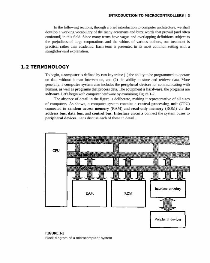
To begin, a computer is defined by two key traits: (1) the ability to be programmed to operateon data without human intervention, and (2) the ability to store and retrieve data. Moregenerally, a computer system also includes the peripheral devices for communicating withhumans, as well as programs that process data. The equipment is hardware, the programs aresoftware. Let's begin with computer hardware by examining Figure 1-2.
The absence of detail in the figure is deliberate, making it representative of all sizesof computers. As shown, a computer system contains a central processing unit (CPU)connected to random access memory (RAM) and read-only memory (ROM) via theaddress bus, data bus, and control bus. Interface circuits connect the system buses toperipheral devices. Let's discuss each of these in detail.
FIGURE 1-2Block diagram of a microcomputer system

4 | CHAPTER 1
1.3 THE CENTRAL PROCESSING UNIT
The CPU, as the "brain" of the computer system, administers all activity in the system and per-forms all operations on data. Most of the CPU's mystique is undeserved, since it is just a col-lection of logic circuits that continuously performs two operations: fetching instructions andexecuting instructions. The CPU has the ability to understand and execute instructions based ona set of binary codes, each representing a simple operation. These instructions are usuallyarithmetic (add, subtract, multiply, divide), logic (AND, OR, NOT, etc.), data movement, orbranch operations, and are represented by a set of binary codes called the instruction set.
Figure 1-3 is an extremely simplified view of the inside of a CPU. It shows a set ofregisters for the temporary storage of information, an arithmetic and logic unit (ALU) forperforming operations on this information, an instruction decode and control unit that de-termines the operation to perform and sets in motion the necessary actions to perform it,and two additional registers. The instruction register (IR) holds the binary code for eachinstruction as it is executed, and the program counter (PC) holds the memory address ofthe next instruction to be executed.
Fetching an instruction from the system RAM or ROM is one of the most funda-mental operations performed by the CPU. It involves the following steps: (a) the contentsof the program counter are placed on the address bus, (b) a READ control signal isactivated, (c) data (the instruction opcode) are read from RAM and placed on the data bus,(d) the op-code is latched into the CPU's internal instruction register, and (e) the programcounter is incremented to prepare for the next fetch from memory. Figure 1-4 illustratesthe flow of information for an instruction fetch.
The execution stage involves decoding (or deciphering) the opcode and generating con-trol signals to gate internal registers in and out of the ALU and to signal the ALU to perform
FIGURE 1-3
The central processing unit
(CPU)

INTRODUCTION TO MICROCONTROLLERS | 5
FIGURE 1-4
Bus activity for an opcode fetch cycle
the specified operation. Due to the wide variety of possible operations, this explanation issomewhat limited in scope. It applies to a simple operation such as "increment register."More complex instructions require more steps, such as reading a second and third byte asdata for the operation.
A series of instructions combined to perform a meaningful task is called a program,or software, and herein is the real mystique. The degree to which tasks are efficiently andcorrectly carried out is determined for the most part by the quality of software, not by thesophistication of the CPU. Programs, then, "drive" the CPU, and in doing so they occa-sionally go amiss, mimicking the frailties of their authors. Phrases such as "The computermade a mistake" are misguided. Although equipment breakdowns are inevitable, mistakesin results are usually a sign of poor programs or operator error.
1.4 SEMICONDUCTOR MEMORY: RAM AND ROM
Programs and data are stored in memory. The variations of computer memory are so vast,their accompanying terms so plentiful, and technology breakthroughs so frequent, that ex-tensive and continual study is required to keep abreast of the latest developments. Thememory devices directly accessible by the CPU consist of semiconductor ICs (integratedcircuits) called RAM and ROM. There are two features that distinguish RAM and ROM:first, RAM is read/write memory while ROM is read-only memory; and second, RAM isvolatile (the contents are lost when power is removed), while ROM is nonvolatile.
Most computer systems have a disk drive and a small amount of ROM, just enoughto hold the short, frequently used software routines that perform input/output operations.

6 | CHAPTER 1
User programs and data are stored on disk and are loaded into RAM for execution. Withthe continual drop in the per-byte cost of RAM, small computer systems often containmillions of bytes of RAM.
1.5 THE BUSES: ADDRESS, DATA, AND CONTROL
A bus is a collection of wires carrying information with a common purpose. Access to thecircuitry around the CPU is provided by three buses: the address bus, data bus, andcontrol bus. For each read or write operation, the CPU specifies the location of the data(or instruction) by placing an address on the address bus and then activates a signal on thecontrol bus, indicating whether the operation is a read or write. Read operations retrieve abyte of data from memory at the location specified and place it on the data bus. The CPUreads the data and places it in one of its internal registers. For a write operation, the CPUoutputs data on the data bus. Because of the control signal, memory recognizes theoperation as a write cycle and stores the data in the location specified.
Most small computers have 16 or 20 address lines. Given n address lines, each with thepossibility of being high (1) or low (0), 2n locations can be accessed. A 16-bit address bus,therefore, can access 216 = 65,536 locations, and a 20-bit address can access 220 = 1,048,576locations. The abbreviation K (for kilo) stands for 210 = 1024; therefore, 16 bits can address26 x 210 = 64K locations, whereas 20 bits can address 1024K or 1 M locations. Theabbreviation M (for mega) stands for 220 = 1024 x 1024 = 1024K = 1,048,576.
The data bus carries information between the CPU and memory or between the CPUand I/O devices. Extensive research effort has been expended in determining the sort of ac-tivities that consume a computer's valuable execution time. Evidently computers spend upto two thirds of their time simply moving data. Since the majority of move operations arebetween a CPU register and external RAM or ROM, the number of lines (the width) of thedata bus is important for overall performance. This limitation-by-width is a bottleneck:There may be vast amounts of memory on the system, and the CPU may possess tremen-dous computational power, but access to the data—data movement between the memoryand CPU via the data bus—is bottlenecked by the width of the data bus.
This trait is so important that it is common to add a prefix indicating the extent ofthis bottleneck. The phrase "16-bit computer" refers to a computer with 16 lines on its databus. Most computers fit the 4-bit, 8-bit, 16-bit, or 32-bit classification, with overallcomputing power increasing as the width of the data bus increases.
Note that the data bus, as shown in Figure 1-2, is bidirectional, and the address busis unidirectional. Address information is always supplied by the CPU (as indicated by thearrow in Figure 1-2), yet data may travel in either direction depending on whether a reador write operation is intended.1 Note also that the term "data" is used in a general sense:the "information" that travels on the data bus may be the instructions of a program, anaddress appended to an instruction, or the data used by the program.
1Address information is sometimes also provided by direct memory access (DMA) circuitry (in
addition to the CPU).
INTRODUCTION TO MICROCONTROLLERS | 7
The control bus is a hodgepodge of signals, each having a specific role in the orderlycontrol of system activity. As a rule, control signals are timing signals supplied by the CPUto synchronize the movement of information on the address and data buses. Although thereare usually three signals, such as CLOCK, READ, and WRITE, for basic data movementbetween the CPU and memory, the names and operation of these signals are highly de-pendent on the specific CPU. The manufacturer's data sheets must be consulted for details.
1.6 INPUT/OUTPUT DEVICES
I/O devices, or "computer peripherals," provide the path for communication between thecomputer system and the "real world." Without these, computer systems would be ratherintroverted machines, of little use to the people who use them. Three classes of I/Odevices are mass storage, human interface, and control/monitor.
1.6.1 Mass Storage Devices
Like semiconductor RAMS and ROMs, mass storage devices are players in the arena ofmemory technology—constantly growing, ever improving. As the name suggests, they holdlarge quantities of information (programs or data) that cannot fit into the computer'srelatively small RAM or "main" memory. This information must be loaded into main mem-ory before the CPU accesses it. Classified according to ease of access, mass storage devicesare either online or archival. Online storage, usually on magnetic disk, is available to theCPU without human intervention upon the request of a program, and archival storage holdsdata that are rarely needed and require manual loading onto the system. Archival storage isusually on magnetic tapes or disks, although optical discs, such as CD-ROM or WORMtechnology, are now emerging and may alter the notion of archival storage due to their re-liability, high capacity, and low cost.2
1.6.2 Human Interface Devices
The union of human and machine is realized by a multitude of human interface devices,the most common being the video display terminal (VDT) and printer. Although printersare strictly output devices that generate hardcopy output, VDTs are really two devices,since they contain a keyboard for input and a CRT (cathode-ray tube) for output. An entirefield of engineering, called "ergonomics" or "human factors," has evolved from thenecessity to design these peripheral devices with humans in mind, the goal being the safe,comfortable, and efficient mating of the characteristics of people with the machines theyuse. Indeed, there are more companies that manufacture this class of peripheral devicethan companies that manufacture computers. For most computer systems, there are at leastthree of these devices: a keyboard, CRT, and printer. Other human interface devicesinclude the joystick, light pen, mouse, microphone, and loudspeaker.
2"CD-ROM" stands for compact-disc read-only memory. "WORM" stands for write-once read-mostly. A CD-
ROM contains 700 Mbyte of storage, enough to store the entire 32 volumes of Encyclopedia Britannica.

8 | CHAPTER 1
1.6.3 Control/Monitor Devices
By way of control/monitor devices (and some meticulously designed interface electronicsand software), computers can perform a myriad of control-oriented tasks, and perform themunceasingly, without fatigue, far beyond the capabilities of humans. Applications such astemperature control of a building, home security, elevator control, home appliance control,and even welding parts of an automobile, are all made possible using these devices.
Control devices are outputs, or actuators, that can affect the world around themwhen supplied with a voltage or current (e.g., motors and relays). Monitoring devices areinputs, or sensors, which are stimulated by heat, light, pressure, motion, etc., and convertthis energy to a voltage or current read by the computer (e.g., phototransistors,thermistors, and switches). The interface circuitry converts the voltage or current to binarydata, or vice versa, and through software an orderly relationship between inputs andoutputs is established. The hardware and software interfacing of these devices tomicrocontrollers is one of the main themes in this book.
1.7 PROGRAMS: BIG AND SMALL
The preceding discussion has focused on computer systems hardware with only a passingmention of the programs, or software, that make them work. The relative emphasis placedon hardware versus software has shifted dramatically in recent years. Whereas the earlydays of computing witnessed the materials, manufacturing, and maintenance costs of com-puter hardware far surpassing the software costs, today, with mass-produced LSI (large-scale integrated) chips, hardware costs are less dominant. It is the labor-intensive job ofwriting, documenting, maintaining, updating, and distributing software that constitutes thebulk of the expense in automating a process using computers.
Let's examine the different types of software. Figure 1-5 illustrates three levels ofsoftware between the user and the hardware of a computer system: the application soft-ware, the operating system, and the input/output subroutines.
At the lowest level, the input/output subroutines directly manipulate the hardware ofthe system, reading characters from the keyboard, writing characters to the CRT, readingblocks of information from the disk, and so on. Since these subroutines are so intimatelylinked to the hardware, they are written by the hardware designers and are (usually) storedin ROM. (They are the BIOS—basic input/output system—on the IBM PC, for example.)
To provide close access to the system hardware for programmers, explicit entry andexit conditions are defined for the input/output subroutines. One only needs to initializevalues in CPU registers and call the subroutine; the action is carried out with resultsreturned in CPU registers or left in system RAM.
As well as a full complement of input/output subroutines, the ROM contains a start-upprogram that executes when the system is powered up or reset manually by the operator. Thenonvolatile nature of ROM is essential here since this program must exist upon power-up."Housekeeping" chores, such as checking for options, initializing memory, performing diag-nostic checks, etc., are all performed by the start-up program. Last, but not least, a bootstraploader routine reads the first track (a small program) from the disk into RAM and passes con-trol to it. This program then loads the RAM-resident portion of the operating system (a large

INTRODUCTION TO MICROCONTROLLERS | 9
program) from the disk and passes control to it, thus comThere is a saying that "the system has pulled itself up by
The operating system is a large collection of progsystem and provide the mechanism to access, manage, anresources. These abilities exist through the operating sutility programs, which in turn facilitate the developmeapplications software is well designed, the user interactsknowledge of the operating system. Providing an effeinterface is a prime objective in the design of applications
1.8 MICROS, MINIS, AND MAINFRAMES
Using their size and power as a starting point, we classminicomputers, or mainframe computers. A key trait of maging of the CPU: It is contained within a single integratthe other hand, minicomputers and mainframe computers,every architectural detail, have CPUs consisting of mult(minicomputers) to several circuit boards of ICs (mainfnecessary to achieve the high speeds and computational po
Typical microcomputers such as the IBM PC, AAmiga incorporate a microprocessor as their CPU. The Rrequire many ICs, with the component count often incrterface circuits vary considerably in complexity, dependin
FIGURE 1-5
Levels of software
pleting the start-up of the system.its own bootstraps."
rams that come with the computerd effectively utilize the computer'system's command language andnt of applications software. If thewith the computer with little or noctive, meaningful, and safe usersoftware.
ify computers as microcomputers,icrocomputers is the size and pack-ed circuit—a microprocessor. Onas well as being more complex in
iple ICs, ranging from several ICsrames). This increased capacity iswer of larger computers.pple Macintosh, and CommodoreAM, ROM, and interface circuits
easing with computing power. In-g on the I/O devices. Driving the

10 | CHAPTER 1
loudspeaker contained in most microcomputers, for example, requires only a couple of logicgates. The disk interface, however, usually involves many ICs, some in LSI packages.
Another feature separating micros from minis and mainframes is that microcomputers aresingle-user, single-task systems-they interact with one user, and they execute one program at atime Minis and mainframes, on the other hand, are multiuser, multitasking systems-they canaccommodate many users and programs simultaneously. Actually, the simultaneous executionof programs is an illusion resulting from "time slicing" CPU resources. (Multiprocessingsystems, however, use multiple CPUs to execute tasks simultaneously.)
1.9 MICROPROCESSORS VS. MICROCONTROLLERS
It was pointed out above that microprocessors are single-chip CPUs used in microcomputers.How, then, do microcontrollers differ from microprocessors? This question can be addressedfrom three perspectives: hardware architecture, applications, and instruction set features.
1.9.1 Hardware Architecture
To highlight the difference between microcontrollers and microprocessors, Figure 1-2 is
redrawn in Figure 1-6, showing more detail.Whereas a microprocessor is a single-chip CPU, a microcontroller contains, in a sin-
gle IC, a CPU and much of the remaining circuitry of a complete microcomputer system.The components within the dotted line in Figure 1-6 are an integral part of most micro-controller ICs. As well as the CPU, microcontrollers include RAM, ROM, a serialinterface, a parallel interface, timer, and interrupt scheduling circuitry—all within the sameIC. Of course, the amount of on-chip RAM does not approach that of even a modestmicrocomputer system; but, as we shall learn, this is not a limitation, since microcontrollersare intended for vastly different applications.
An important feature of microcontrollers is the built-in interrupt system. As control-oriented devices, microcontrollers are often called upon to respond to external stimuli(interrupts) in real time. They must perform fast context switching, suspending oneprocess while executing another in response to an "event." The opening of a microwaveoven's door is an example of an event that might cause an interrupt in a microcontroller-based product. Of course, most microprocessors can also implement powerful interruptschemes, but external components are usually required. A microcontroller's on-chipcircuitry includes all the interrupt handling circuitry necessary.
1.9.2 Applications
Microprocessors are most commonly used as the CPU in microcomputer systems. Thisfunction is what they are designed for, and this is where their strengths lie. Microcontrollers,however, are found in small, minimum-component designs performing control-oriented ac-tivities. These designs were often implemented in the past, using dozens or even hundreds ofdigital ICs. A microcontroller can aid in reducing the overall component count. All that isrequired is a microcontroller, a small number of support components, and a control program

INTRODUCTION TO MICROCONTROLLERS | 11
FIGURE 1-6Detailed block diagram of a microcomputer system
in ROM. Microcontrollers are suited to "control" of I/O devices in designs requiring aminimum component count, whereas microprocessors are suited to "processing"information in computer systems.
1.9.3 Instruction Set Features
Due to the deficiencies in applications, microcontrollers have somewhat different requirementsfor their instruction sets than microprocessors. Microprocessor instruction sets are "processingintensive," implying they have powerful addressing modes with instructions catering to oper-ations on large volumes of data. Their instructions operate on nibbles, bytes, words, or evendouble words.3 Addressing modes provide access to large arrays of data, using address pointersand offsets. Auto-increment and auto-decrement modes simplify stepping through arrays onbyte, word, or double-word boundaries. Privileged instructions cannot execute within the userprogram. The list goes on.
3The most common interpretation of these terms is 4 bits = 1 nibble, 8 bits = 1 byte, 16 bits = 1 word,and 32 bits = 1 double word.
12 | CHAPTER 1
Microcontrollers, on the other hand, have instruction sets catering to the control ofinputs and outputs. The interface to many inputs and outputs uses a single bit. Forexample, a motor may be turned on and off by a solenoid energized by a 1-bit output port.Micro-controllers have instructions to set and clear individual bits and perform other bit-oriented operations such as logically ANDing, ORing, or EXORing bits, jumping if a bit isset or clear, and so on. This powerful feature is rarely present in microprocessors, whichare usually designed to operate on bytes or larger units of data.
In the control and monitoring of devices (perhaps with a 1-bit interface), microcon-trollers have built-in circuitry and instructions for input/output operations, event timing,and enabling and setting priority levels for interrupts caused by external stimuli. Micro-processors often require additional circuitry (serial interface ICs, interrupt controllers,timers, etc.) to perform similar operations. Nevertheless, the sheer processing capability ofa microcontroller never approaches that of a microprocessor (all else being equal), since agreat deal of the IC's "real estate" is consumed by the on-chip functions—at the expense ofprocessing power, of course.
Since the on-chip real estate is at a premium in microcontrollers, the instructions mustbe extremely compact, with the majority implemented in a single byte. A design criterion isoften that the control program must fit into the on-chip ROM, since the addition of evenone external ROM adds too much cost to the final product. A tight encoding scheme for theinstruction set is essential. This is rarely a feature of microprocessors; their powerful ad-dressing modes bring with them a less-than-compact encoding of instructions.
1.10 NEW CONCEPTS
Microcontrollers, like other products considered in retrospect to have been a breakthrough,have arrived out of two complementary forces: market need and new technology. The newtechnology is just that mentioned above: semiconductors with more transistors in lessspace, mass produced at a lower cost. The market need is the industrial and consumer ap-petite for more sophisticated tools and toys.4 This demand encompasses a lot of territory.The most illustrative example, perhaps, is the automobile dashboard. Witness the transfor-mation of the car's "control center" over the past decade—made possible by the microcon-troller and other technological developments. Once, drivers were content to know theirspeed; today they may find a display of fuel economy and estimated time of arrival. Onceit was sufficient to know if a seatbelt was unfastened while starting the car; today, we are"told" which seatbelt is the culprit. If a door is ajar, we are again duly informed by thespoken word. (Perhaps the seatbelt is stuck in the door.)
This brings to mind a necessary comment. Microprocessors (and in this sense micro-controllers) have been dubbed "solutions looking for a problem." It seems they have provedso effective at reducing the complexity of circuitry in (consumer) products, that manufac-turers are often too eager to include superfluous features simply because they are easy to
41t is sometimes argued that "market need" is really "market want," spurred on by the self-propelled growth oftechnology.

INTRODUCTION TO MICROCONTROLLERS | 13
design into the product. The result often lacks eloquence—a showstopper initially, but anannoyance finally. The most stark example of this bells-and-whistles approach occurs inthe recent appearance of products that talk. Whether automobiles, toys, or toasters, theyare usually examples of tackiness and overdesign-1980s art deco, perhaps. Rest assuredthat once the dust has settled and the novelty has diminished, only the subtle andappropriate will remain.
Microcontrollers are specialized. They are not used in computers per se, but inindustrial and consumer products. Users of such products are quite often unaware ofthe existence of microcontrollers: to them, the internal components are but an inconse-quential detail of design. Consider as examples microwave ovens, programmable ther-mostats, electronic scales, and even cars. The electronics within each of these productstypically incorporates a microcontroller interfacing to push buttons, switches, lights,and alarms on a front panel; yet user operation mimics that of the electromechanicalpredecessors, with the exception of some added features. The microcontroller is invisi-ble to the user.
Unlike computer systems, which are defined by their ability to be programmed andthen reprogrammed, microcontrollers are permanently programmed for one task. Thiscomparison results in a stark architectural difference between the two. Computer systemshave a high RAM-to-ROM ratio, with user programs executing in a relatively large RAMspace and hardware interfacing routines executing in a small ROM space. Microcontrollers,on the other hand, have a high ROM-to-RAM ratio. The control program, perhapsrelatively large, is stored in ROM, while RAM is used only for temporary storage. Sincethe control program is stored permanently in ROM, it has been dubbed firmware. Indegrees of "firmness," it lies somewhere between software—the programs in RAM that arelost when power is removed—and hardware—the physical circuits. The difference betweensoftware and hardware is somewhat analogous to the difference between a page of paper(hardware) and words written on a page (software). Consider firmware as a standard formletter, designed and printed for a single purpose.
1.11 GAINS AND LOSSES: A DESIGN EXAMPLE
The tasks performed by microcontrollers are not new. What is new is that designs are im-plemented with fewer components than before. Designs previously requiring tens or evenhundreds of ICs are implemented today with only a handful of components, including amicrocontroller. The reduced component count, a direct result of the microcontroller's pro-grammability and high degree of integration, usually translates into shorter developmenttime, lower manufacturing cost, lower power consumption, and higher reliability. Logicoperations that require several ICs can often be implemented within the microcontroller,with the addition of a control program.
One tradeoff is speed. Microcontroller-based solutions are never as fast as the dis-crete counterparts. Situations requiring extremely fast response to events (a minority of ap-plications) are poorly handled by microcontrollers. For example, consider in Figure 1-7 thesomewhat trivial implementation of the NAND operation using an 8051 microcontroller.

14 | CHAPTER 1
It is not at all obvious that a microcontroller could be used for such an operation, butit can. The software must perform the operations shown in the flowchart in Figure 1-8.The 8051 assembly language program for this logic operation is shown below.
LOOP: MOV C,P1.4 ;READ P1.4 BIT INTO CARRY FLAGANL C,P1.5 ;AND WITH P1.5ANL C,P1.6 ;AND WITH P1.6CPL C ;CONVERT TO "NAND" RESULTMOV P1.7,C ;SEND TO P1.7 OUTPUT BITSJMP LOOP ;REPEAT
If this program executes on an 8051 microcontroller, indeed the 3-input NANDfunction is realized. (It could be verified with a voltmeter or oscilloscope.) The propa-gation delay from an input transition to the correct output level is quite long, at least incomparison to the equivalent TTL (transistor-transistor logic) circuit. Depending on whenthe input changed relative to the program sensing the change, the delay is from 3 to 17microseconds. (This assumes standard 8051 operation using a 12 MHz crystal.) Theequivalent TTL propagation delay is on the order of 10 nanoseconds—about three ordersof magnitude less. Obviously, there is no contest when comparing the speed of micro-controllers with TTL implementations of the same function.
In many applications, particularly those with human operation, whether the delaysare measured in nanoseconds, microseconds, or milliseconds is inconsequential. (Whenthe oil pressure drops in your car, do you need to be informed within microseconds?) Thelogic gate example illustrates that microcontrollers can implement logic operations.Furthermore, as designs become complex, the advantages of the microcontroller-baseddesign begin to take hold. The reduced component count has advantages, as mentionedearlier; but, also, the operations in the control program make it possible to introducechanges in design by modifying only the software. This modification has minimal impacton the manufacturing cycle.
This concludes our introduction to microcontrollers. In the next chapter, we beginour examination of the MCS-51TM family of devices.
PROBLEMS
1.1 What was the first widely used microprocessor? In what year was it introduced andby what company?
FIGURE 1-7
Microcontroller implementation of a simple
logic operation

INTRODUCTION TO MICROCONTROLLERS | 15
FIGURE 1-8
Flowchart for logic gate
program
1.2 Two of the smaller microprocessor companies in the 1970and Zilog. Name the microprocessor that each of these com
1.3 What year was the 8051 microcontroller introduced? Whthe 8051, and in what year was it introduced?
1.4 Name the two types of semiconductor memory discussed inretains its contents when powered-off? What is the commoproperty?
1.5 Which register in a CPU always contains an address? Whthis register?
1.6 During an opcode fetch, what is the information on theWhat is the direction of information flow on these buses du
1.7 How many bytes of data can be addressed by a computaddress bus and an 8-bit data bus?
1.8 What is the usual meaning of "16-bit" in the phrase "16-bit1.9 What is the difference between online storage and archival1.10 What type of technology is used for archival storage beside
s were MOS Technologypanies introduced.
at was the predecessor to
this chapter. Which typen term that describes this
at address is contained in
address and data buses?ring an opcode fetch?er system with an 18-bit
computer"?storage?
s magnetic tape and disk?
16 | CHAPTER 1
1.11 With regard to computing systems, what is the goal of the field of engineeringknown as "human factors"?
1.12 Consider the following human interface devices: a joystick, a light pen, a mouse,a microphone, and a loudspeaker. Which are input devices? Which are output devices?
1.13 Of the three levels of software presented in this chapter, which is the lowest level?What is the purpose of this level of software?
1.14 What is the difference between an actuator and a sensor? Give an example of each.1.15 What is firmware? Comparing a microcontroller-based system to a micro-
processor-based system, which is more likely to rely on firmware? Why?1.16 What is an important feature of a microcontroller's instruction set that dis-
tinguishes it from a microprocessor?1.17 Name five products not mentioned in this chapter that are likely to use a microcontroller.

Hardware Summary
2.1 MCS-51TM FAMILY OVERVIEW
The MCS-51TM is a family of microcontroller ICs developed, manufactured, and marketedby Intel Corporation. Other IC manufacturers, such as Siemens, Advanced Micro Devices,Fujitsu, and Philips are licensed "second source" suppliers of devices in the MCS-51TM
family. Each microcontroller in the family boasts a complement of features suited to a par-ticular design setting.
In this chapter the hardware architecture of the MCS-51TM family is introduced. In-tel's data sheet for the entry-level devices (e.g., the 8051AH) is found in Appendix E. Thisappendix should be consulted for further details, for example, on electrical properties ofthese devices.
Many of the hardware features are illustrated with short sequences of instructions.Brief descriptions are provided with each example, but complete details of the instructionset are deferred to Chapter 3. See also Appendix A for a summary of the 8051 instructionset or Appendix C for definitions of each 8051 instruction.
The generic MCS-51TM IC is the 8051, the first device in the family offered com-mercially. Its features are summarized below.
4K bytes ROM (factory mask programmed) 128 bytes RAM Four 8-bit I/O (Input/Output) ports Two 16-bit timers Serial interface 64K external code memory space 64K external data memory space Boolean processor (operates on single bits) 210 bit-addressable locations 4 µs multiply/divide
17
18 | CHAPTER 2
TABLE 2-1
Comparison of MCS-51TM ICs
PartNumber
On-ChipCode Memory
On-ChipData Memory Timers
8051 4 K ROM 128 bytes 28031 0 K 128 bytes 28751 4 K EPROM 128 bytes 28052 8 K ROM 256 bytes 38032 0 K 256 bytes 38752 8 K EPROM 256 bytes 3
Other members of the MCS-51TM family offer different combinations of on-chip ROM or EPROM, on-chip RAM, or a third timer. Each of the MCS-51TM ICsis also offered in a low-power CMOS version (see Table 2-1).
The term "8051" loosely refers to the MCS-51TM family of microcontrollers.When discussion centers on an enhancement to the basic 8051 device, the specificpart number is used. The features mentioned above are shown in the blockdiagram in Figure 2-1. (See also Appendix D.)
2.2 ONCE AROUND THE PINS
This section introduces the 8051 hardware architecture from an externalperspective—the pinouts (see Figure 2-2). A brief description of the function ofeach pin follows.
As evident in Figure 2-2, 32 of the 8051's 40 pins function as I/O port lines.However, 24 of these lines are dual-purpose (26 on the 8032/8052). Each canoperate as I/O, or as a control line or part of the address or data bus.
Designs requiring a minimum of external memory or other externalcomponents use these ports for general purpose I/O. The eight lines in each portcan be treated as a unit in interfacing to parallel devices such as printers, digital-to-analog converters, and so on. Or, each line can operate independently ininterfacing to single-bit devices such as switches, LEDs, transistors, solenoids,motors, and loudspeakers.
2.2.1 Port 0
Port 0 is a dual-purpose port on pins 32-39 of the 8051 IC. In minimum-componentdesigns, it is used as a general purpose I/O port. For larger designs with external memory,it becomes a multiplexed address and data bus. (See 2.7 External Memory.)
2.2.2 Port 1
Port 1 is a dedicated I/O port on pins 1-8. The pins, designated as P1.0, P1.1, P1.2, etc., are
available for interfacing to external devices as required. No alternate functions are as signed

HARDWARE SUMMARY | 19
for Port 1 pins; thus, they are used solely for interfacing to external devices. Exceptionsare the 8032/8052 ICs, which use P1.0 and P1.1 either as I/O lines or as external inputs tothe third timer.
2.2.3 Port 2
Port 2 (pins 21-28) is a dual-purpose port serving as general purpose I/O, or as the high-byte of the address bus for designs with external code memory or more than 256 bytes ofexternal data memory. (See 2.7 External Memory.)
2.2.4 Port 3
Port 3 is a dual-purpose port on pins 10-17. As well as general-purpose i/o, these pins aremultifunctional, with each having an alternate purpose related to special features of the8051. The alternate purpose of the Port 3 and Port 1 pins is summarized in Table 2-2.
20 | CHAPTER 2
FIGURE 2-2
8051 pinouts
2.2.5 PSEN (Program Store Enable)
The 8051 has four dedicated bus control signals. Program Store Enable ( PSEN ) is an out-
put signal on pin 29. It is a control signal that enables external program (code) memory. It
usually connects to an EPROM's (Erasable Programmable Read-Only Memory) Output
Enable ( OE ) pin to permit reading of program bytes.

HARDWARE SUMMARY | 21
TABLE 2-2
Alternate pin functions for port pins
The ( PSEN ) signal pulses low during the fetch stage of an instruction, which is
stored in external program memory. The binary codes of a program (opcodes) are read
from EPROM, travel across the data bus, and are latched into the 8051's instruction
register for decoding. When executing a program from internal ROM (8051/8052),
( PSEN ) remains in the inactive (high) state.
2.2.6 ALE (Address Latch Enable)
The ALE output signal on pin 30 will be familiar to anyone who has worked with Intel's8085, 8088, or 8086 microprocessors. The 8051 similarly uses ALE for demultiplexingthe address and data bus. When Port 0 is used in its alternate mode—as the data bus andthe low-byte of the address busALE is the signal that latches the address into an externalregister during the first half of a memory cycle. This done, the Port 0 lines are thenavailable for data input or output during the second half of the memory cycle, when thedata transfer takes place. (See 2.7 External Memory.)
The ALE signal pulses at 1/6th the on-chip oscillator frequency and can be used as ageneral-purpose clock for the rest of the system. If the 8051 is clocked from a 12 MHzcrystal, the ALE signal oscillates at 2 MHz. The only exception is during the MOVXinstruction, when one ALE pulse is missed. (See Figure 2-11.) This pin is also used for theprogramming input pulse for EPROM versions of the 8051.
2.2.7 EA (External Access)
The EA input signal on pin 31 is generally tied high (+5 V) or low (ground). If high, the
8051/8052 executes programs from internal ROM when executing in the lower 4K/8K of
memory. If low, programs execute from external memory only (and PSEN pulses low
accordingly). EA must be tied low for 8031/8032 ICs, since there is no on-chip program
memory. If EA is tied low on an 8051/8052, internal ROM is disabled and programs exe-
cute from external EPROM. The EPROM versions of the 8051 also use the EA line for the
+21 volt supply (Vpp)for programming the internal EPROM.

22 | CHAPTER 2
2.3 I/O
2.2.8 RST (Reset)
The RST input on pin 9 is the master reset for the 8051. When this signal is brought highfor at least two machine cycles, the 8051 internal registers are loaded with appropriatevalues for an orderly system start-up. For normal operation, RST is low. (See 2.9 ResetOperation.)
2.2.9 On-Chip Oscillator Inputs
As shown in Figure 2-2, the 8051 features an on-chip oscillator that is typically driven by acrystal connected to pins 18 and 19. Stabilizing capacitors are also required as shown.
The nominal crystal frequency is 12 MHz for most ICs in the MCS-51TM family,although the 80C31BH-1 can operate with crystal frequencies up to 16 MHz. The on-chiposcillator needn't be driven by a crystal. As shown in Figure 2-3, a TTL clock source canbe connected to XTAL1 and XTAL2.
2.2.10 Power Connections
The 8051 operates from a single +5 volt supply. The Vcc connection is on pin 40, and theVss (ground) connection is on pin 20.
PORT STRUCTURE
The internal circuitry for the port pins is shown in abbreviated form in Figure 2-4. Writingto a port pin loads data into a port latch that drives a field-effect transistor connected to theport pin. The drive capability is four low-power Schottky TTL loads for Ports 1, 2, and 3;and eight LS loads for Port 0. (See Appendix E for more details.) Note that the pull-upresistor is absent on Port 0 (except when functioning as the external address/data bus). Anexternal pull-up resistor may be needed, depending on the input characteristics of thedevice driven by the port pin.
There is both a "read latch" and "read pin" capability. Instructions that require a read-modify-write operation (e.g., CPL P1.5) read the latch to avoid misinterpreting the voltagelevel in the event the pin is heavily loaded (e.g., when driving the base of a transistor). In-structions that input a port bit (e.g., MOV C,P1.5) read the pin. The port latch must contain
FIGURE 2-3
Driving the 8051 from a TTL oscillator

HARDWARE SUMMARY | 23
FIGURE 2-4Circuitry for I/O ports
a 1, in this case, otherwise the FET driver is ON and pulls tile output low. A system resetsets all port latches, so port pins may be used as inputs without explicitly setting tile portlatches. If, however, a port latch is cleared (e.g., CLR P1.5), then it cannot function subse-quently as an input unless the latch is set first (e.g., SETB P1.5).
Figure 2-4 does not show the circuitry for the alternate functions for Ports 0, 2, and3. When the alternate function is in effect, the output drivers are switched to an internaladdress (Port 2), address/data (Port 0), or control (Port 3) signal, as appropriate.
2.4 TIMING AND THE MACHINE CYCLE
The 8051's on-chip oscillator is driven by an external quartz crystal through pins 18 and19. This crystal has a typical frequency of 12 MHz, meaning that it generates 12 millionclock cycles per second. These oscillator clock cycles form the basis of the 8051's timingand synchronization: Every operation performed by the 8051 is in step with these cycles.
With the oscillator clock as reference, the 8051 requires two such clock cycles to per-form a single discrete operation, which is either fetching an instruction, decoding, or exe-cuting it. This duration of two clock cycles is also called a state. Therefore, in order to fullyprocess an instruction, the 8051 would generally require six such states, or 12 clock cyclessince it would have to first fetch and decode the instruction before it goes to execute it. Thisduration of six states is also known as one machine cycle. Of course, more complex in-structions would take more than one machine cycle to be carried out. Both Appendix B andC provide a list of the number of machine cycles for all the 8051 instructions. This numberranges from one to four machine cycles. Figure 2-5 shows the relationship between oscillatorclock cycles (P), states (S), and a machine cycle.
Typically, the 8051's on-chip oscillator, fosc is driven by a 12 MHz crystal, so theperiod of one clock pulse, Tclock = 1/fosc = 1/12 MHz = 83.33 ns. One machine cycle con-sists of 12 such clock pulses, hence its duration is 83.33 ns x 12 = 1 µs.
24 | CHAPTER 2
2.5 MEM
ORY ORGANIZATIONMost microprocessors implement a shared memory space for data and programs. This isreasonable, since programs are usually stored on a disk and loaded into RAM for execu-tion; thus both the data and programs reside in the system RAM. Microcontrollers, on theother hand, are rarely used as the CPU in "computer systems." Instead, they are employedas the central component in control-oriented designs. There is limited memory, and there isno disk drive or disk operating system. The control program must reside in ROM.
For this reason, the 8051 implements a separate memory space for programs (code)and data. As shown in Table 2-1, both the code and data may be internal; however, bothexpand using external components to a maximum of 64K code memory and 64K datamemory.
The internal memory consists of on-chip ROM (8051/8052 only) and on-chip dataRAM. The on-chip RAM contains a rich arrangement of general-purpose storage, bit-addressable storage, register banks, and special function registers.
Two notable features are: (a) the registers and input/output ports are memory mappedand accessible like any other memory location, and (b) the stack resides within the internalRAM, rather than in external RAM as typical of microprocessors.
Figure 2-6 summarizes the memory spaces for the ROM-less 8031 device withoutshowing any detail of the on-chip data memory. (8032/8052 enhancements are summarizedlater.)
Figure 2-7 gives the details of the on-chip data memory. As shown, the internal datamemory space is divided between internal RAM (00H-7FH) and special function regis-ters (80H-0FFH). A confusion sometimes arises between the concept of internal (on-chip)data memory and internal RAM. The 8051's internal data memory space has the range from00H-0FFH, which is 256 bytes. However, only the lower half (00H-7FH) of the internalmemory space is for general data while the upper half (80H-0FFH) is mostly for specificpurposes and not for general data; hence, only the lower half is considered to be internalRAM. The internal data RAM is further sub-divided into register banks (00H-1FH), bit-addressable RAM (20H-2FH), and general-purpose RAM (30H-7FH). Each of these sec-tions of internal memory is discussed below.
2.5.1 General-Purpose RAM
Although Figure 2-7 shows 80 bytes of general-purpose RAM from addresses 30H to 7FH,the bottom 48 bytes from 00H to 2FH can be used similarly (although these locations haveother purposes as discussed below).
FIGURE 2-5
Relationship between oscillator
clock cycles, states, and the
machine cycle

HARDWARE SUMMARY | 25
FIGURE 2-6
Summary of the 8031 memory spaces
Any location in the general-purpose RAM can be accessed freely using the direct orindirect addressing modes. For example, to read the contents of internal RAM address5FH into the accumulator, the following instruction could be used:
MOV A,5FH
This instruction moves a byte of data using direct addressing to specify the "source location"(i.e., address 5FH). The destination for the data is implicitly specified in the instruction op-code as the A accumulator. (Note: Addressing modes are discussed in detail in Chapter 3.)
Internal RAM can also be accessed using indirect addressing through R0 or R1. Forexample, the following two instructions perform the same operation as the single instruc-tion above:
MOV R0,#5FH
MOV A,@R0
The first instruction uses immediate addressing to move the value 5FH into register R0,and the second instruction uses indirect addressing to move the data "pointed at by R0"into the accumulator.

26 | CHAPTER 2
FIGURE 2-7
Summary of the 8051 on-chip data memory
2.5.2 Bit-Addressable RAM
The 8051 contains 210 bit-addressable locations, of which 128 are at byte addresses 20Hthrough 2FH, and the rest are in the special function registers (discussed below).
The idea of individually accessing bits through software is a powerful feature ofmost microcontrollers. Bits can be set, cleared, ANDed, ORed, etc., with a singleinstruction. Most microprocessors require a read-modify-write sequence of instructions toachieve the same effect. Furthermore, the 8051 I/O ports are bit-addressable, simplifyingthe software interface to single-bit inputs and outputs.

HARDWARE SUMMARY | 27
There are 128 general-purpose bit-addressable locations at byte addresses 20Hthrough 2FH (8 bits/byte x 16 bytes = 128 bits). These addresses are accessed as bytes oras bits, depending on the instruction. For example, to set bit 67H, the following instructioncould be used:
SETB 67H
Referring to Figure 2-7, note that "bit address 67H" is the most-significant bit at"byte address 2CH." The instruction above has no effect on the other bits at this address.Most microprocessors would perform the same operation as follows:
MOV A, 2CH ;READ ENTIRE BYTEORL A,#10000000B ;SET MOST-SIGNIFICANT BITMOV 2CH,A ;WRITE BACK ENTIRE BYTE
EXAMPLE What instruction would be used to set bit 3 in byte address 25H?2.1
Solution
SETB 2BH
Discussion
Byte address 25H is within the bit-addressable area of internal memory (see Figure 2-7).The bit addresses within this byte, starting at bit 0, are 28H, 29H, etc. Bit 3 within byte ad-dress 25H is at bit address 2BH.
2.5.3 Register Banks
The bottom 32 locations of internal memory contain the register banks. The 8051 instruc-tion set supports eight registers, R0 through R7, and by default (after a system reset) theseregisters are at addresses 00H-07H. The following instruction, then, reads the contents ofaddress 05H into the accumulator:
MOV A,R5
This instruction is a 1-byte instruction using register addressing. Of course, the same oper-ation could be performed in a 2-byte instruction, using the direct address as byte 2:
MOV A,05H
Instructions using registers R0 to R7 are shorter than the equivalent instructionsusing direct addressing. Data values used frequently should use one of these registers.
The active register bank may be altered by changing the register bank select bits inthe program status word (discussed below). Assuming, then, that register bank 3 is active,the following instruction writes the contents of the accumulator into location 18H:
MOV R0,A

28 | CHAPTER 2
The idea of "register banks" permits fast and effective "context switching," wherebyseparate sections of software use a private set of registers independent of other sections ofsoftware.
EXAMPLE What is the address of register 5 in register bank 3?
2.2 Solution
1DH
Discussion
Register bank 3 occupies internal memory locations 18H to 1FH (see Figure 2-7), with R0at address 18H, R1 at address 19H, etc. Register 5 (R5) is at address 1DH.
2.6 SPECIAL FUNCTION REGISTERS
Internal registers on most microprocessors are accessed implicitly by the instruction set.For example, "INCA" on the 6809 microprocessor increments the contents of the A accu-mulator. The operation is specified implicitly within the instruction opcode. Similar accessto registers is also used on the 8051 microcontroller. In fact, the 8051 instruction "INC A"performs the same operation.
The 8051 internal registers are configured as part of the on-chip RAM: therefore,each register also has an address.1 This is reasonable for the 8051, since it has so many reg-isters. As well as R0 to R7, there are 21 special function registers (SFRs) at the top ofinternal RAM, from addresses 80H to 0FFH. (See Figure 2-7 and Appendix D.) Note thatmost of the 128 addresses from 80H to 0FFH are not defined. Only 21 SFR addresses aredefined (26 on the 8032/8052).
Although the accumulator (A or ACC) may be accessed implicitly as shown previ-ously, most SFRs are accessed using direct addressing. Note in Figure 2-7 that some SFRsare both bit-addressable and byte-addressable. Programmers should be careful when ac-cessing bits versus bytes. For example, the instruction
SETB 0E0H
sets bit 0 in the accumulator, leaving the other bits unchanged. The trick is to recognizethat 0E0H is both the byte address of the entire accumulator and the bit address of theleast-significant bit in the accumulator. Since the SETB instruction operates on bits (notbytes), only the addressed bit is affected. Notice that the addressable bits within theSFRs have the five high-order address bits matching those of the SFR. For example, Port1 is at byte address 90H or 10010000B. The bits within Port 1 have addresses 90H to97H, or 10010xxxB.
1The program counter and the instruction register are exceptions. Since these registers are rarely manipulateddirectly, nothing is gained by placing them in the on-chip RAM.

HARDWARE SUMMARY | 29
EXAMPLE What instruction could be used to set the most-significant bit in the B accumulator while2.3 leaving the other bits intact?
Solution
SETB 0F7H
Discussion
The B accumulator is at byte address 0F0H in the special function register space ofinternal memory (see Figure 2-7). Individual bits are accessible, with bit 0 at address0F0H, bit 1 at address 0F1H, etc. Bit 7 of the B accumulator is at bit address 0F7H.
The PSW is discussed in detail in the following section. The other SFRs are brieflyintroduced following the PSW, with detailed discussions deferred to later chapters.
2.6.1 Program Status Word
The program status word (PSW) at address 0D0H contains status bits as summarized inTable 2-3. Each of the PSW bits is examined below.
2.6.1.1 Carry Flag The carry flag (C or CY) is dual-purpose. It is used in thetraditional way for arithmetic operations: set if there is a carry out of bit 7 during an add,or set if there is a borrow into bit 7 during a subtract. For example, if the accumulatorcontains 0FFH, then the instruction
ADD A,#1
leaves the accumulator equal to 00H and sets the carry flag in the PSW.

30 | CHAPTER 2
EXAMPLE What is the state of the carry flag and the content of the accumulator after execution of the2.4 following instruction sequence?
MOV R5,#55HMOV A,#0AAHADD A,R5
Solution
C = 0, ACC = 0FFH
Discussion
The binary addition that occurs in the third instruction is illustrated below.
01010101 (R5 = 55H)+10101010 (ACC = 0AAH)11111111 (Result in ACC = 0FFH)
The addition does not generate a carry of the most-significant bit (bit 7); therefore, thecarry bit is cleared. The final result in the accumulator is 0FFH = 25510.
The carry flag is also the "Boolean accumulator," serving as a 1-bit register forBoolean instructions operating on bits. For example, the following instruction ANDs bit25H with the carry flag and places the result back in the carry flag:
ANL C,25H
2.6.1.2 Auxiliary Carry Flag When adding binary-coded-decimal (BCD) values,the auxiliary carry flag (AC) is set if a carry was generated out of bit 3 into bit 4 or if theresult in the lower nibble is in the range 0AH-0FH. If the values added are BCD, then theadd instruction must be followed by DA A (decimal adjust accumulator) to bring resultsgreater than 9 back into range.
EXAMPLE What is the state of the auxiliary carry flag and the content of the accumulator after2.5 execution of the instruction sequence below?
MOV R5,#1MOV A,#9ADD A,R5
Solution
AC = 1, ACC = 0AH
Discussion
The binary addition that takes place in the third instruction is illustrated below.
100000001 (R5 = 01H)
+00001001 (ACC = 09H)00001010 (Result in ACC = 0AH)

HARDWARE SUMMARY | 31
Although no carry occurred during the binary addition, the low-order nibble of the result is1010B = 0AH. Since this is greater than 910, the auxiliary carry bit is set. If the additioninstruction is followed by a decimal adjust instruction (DA A), the final result in the accu-mulator is 0001000B 10H. As a binary-coded decimal number, 10H = 1010 which is thecorrect result of 910 + 110.
2.6.1.3 Flag 0 Flag 0 (F0) is a general-purpose flag bit available for user appli-cations.
2.6.1.4 Register Bank Select Bits The register bank select bits (RS0 and RS1)determine the active register bank. They are cleared after a system reset and are changedby software as needed. For example, the following three instructions enable register bank3 and then move the content of R7 (byte address 1FH) to the accumulator:
SETB RS1SETB RS0MOV A,R7
When the above program is assembled, the correct bit addresses are substituted for thesymbols "RS1" and "RS0." Thus, the instruction SETB RS1 is the same as SETB 0D4H.
EXAMPLE Illustrate an instruction sequence to make register bank 2 the active register bank. Assume2.6 that the previously active register bank is unknown.
Solution
SETB RS1CLR RS0
Discussion
The result of the above instructions is to place 102 = 210 in the register bank select bits inthe program status word. The active register bank becomes bank 2. If it was known thatthe register bank bits had not changed since the last CPU reset operation, the secondinstruction would not be necessary; however, since an unknown state was assumed, bothregister select bits are explicitly initialized.
2.6.1.5 Overflow Flag The overflow flag (OV) is set after an addition or sub-traction operation if there was an arithmetic overflow. When signed numbers are added orsubtracted, software can examine this bit to determine if the result is in the proper range.When unsigned numbers are added, the OV bit can be ignored. Results greater than +127or less than -128 will set the OV bit. For example, the following addition causes an over-flow and sets the OV bit in the PSW:
Hex: 0F Decimal: 15
+7F +1278E 142
As a signed number, 8EH represents -116, which is clearly not the correct result of142; therefore, the OV bit is set.

32 | CHAPTER 2
EXAMPLE What is the state of the overflow flag and the content of the accumulator after the execution
2.7 of the following instruction sequence?
MOV R7,#0FFHMOV A,#0FHADD A,R7
Solution
OV = 0, ACC = 0EH
Discussion
R7 is initialized with 0FFH, which as a signed number equals -110. The accumulator is ini-tialized with 0FH, which equals 1510. The result of the addition is 15 + ( -1 ) = 14 = 0EH.Since 14 is within the allowable range for 8-bit signed numbers (-128 to +127), no over-flow occurs and the OV bit is cleared. (Note, however, that the C bit is set because theaddition generates a carry out of bit 7.)
2.6.1.6 Parity Bit The parity bit (P) is automatically set or cleared each machinecycle to establish even parity with the accumulator. The number of 1-bits in the accumula-tor plus the P bit is always even. If, for example, the accumulator contains 10101101, Pwill contain 1 (establishing a total of six 1-bits; i.e., an even number of 1s). The parity bit ismost commonly used in conjunction with serial port routines to include a parity bit beforetransmission or to check for parity after reception.
EXAMPLE What is the state of the P bit after execution of the following instruction?2.8
MOV A,#55H
Solution
P = 0
DiscussionIn binary, 55H equals 01010101B. This pattern has four bits equal to 1. Since 4 is an evennumber, the P bit is set to zero. The total number of bits equal to 1, counting those in theaccumulator and the P bit, is four, thus achieving even parity.
2.6.2 B Register
The B register, or accumulator B, at address 0F0H is used along with the accumulator formultiply and divide operations. The MUL AB instruction multiplies the 8-bit unsigned val-ues in A and B and leaves the 16-bit result in A (low-byte) and B (high-byte). The DIV ABinstruction divides A by B, leaving the integer result in A and the remainder in B. The Bregister can also be treated as a general-purpose scratch-pad register. It is bit-addressablethrough bit addresses 0F0H to 0F7H.
HARDWARE SUMMARY | 33
2.6.3 Stack Pointer
The stack pointer (SP) is an 8-bit register at address 81H. It contains the address of the dataitem currently on the top of the stack. Stack operations include "pushing" data on the stackand "popping" data off the stack. Pushing on the stack increments the SP before writing data,and popping from the stack reads data and then decrements the SP. The 8051 stack is kept ininternal RAM and is limited to addresses accessible by indirect addressing. These are the first128 bytes on the 8031/8051 or the full 256 bytes of on-chip RAM on the 8032/8052.
To reinitialize the SP with the stack beginning at 60H, the following instruction is used:
MOV SP,#5FH
On the 8031/8051 this would limit the stack to 32 bytes, since the uppermost address ofon-chip RAM is 7FH. The value 5FH is used, since the SP increments to 60H before thefirst push operation.
EXAMPLE What instruction would be used to initialize the stack pointer on an 8052 to create a 48-byte2.9 stack at the top of internal memory?
Solution
MOV SP,#0CFH
Discussion
Since the 8052 has 256 bytes of internal memory, a 48-byte stack positioned at the top wouldoccupy locations 0D0H to 0FFH. Since the SP increments before the first item is placed onthe stack, it should be initialized to the address just below the starting location, 0CFH.
Designers may choose not to reinitialize the stack pointer and let it retain its defaultvalue upon system reset. The reset value of 07H maintains compatibility with the 8051'spredecessor, the 8048, and results in the first stack write storing data in location 08H. Ifthe application software does not reinitialize the SP, then register bank 1 (and perhaps 2and 3) is not available, since this area of internal RAM is the stack.
The stack is accessed explicitly by the PUSH and POP instructions to temporarilystore and retrieve data, or implicitly by the subroutine call (ACALL, LCALL) and return(RET, RETI) instructions to save and restore the program counter.
2.6.4 Data Pointer
The data pointer (DPTR), used to access external code or data memory, is a 16-bit registerat addresses 82H (DPL, low-byte) and 83H (DPH, high-byte). The following three instruc-tions write 55H into external RAM location 1000H:
MOV A,#55HMOV DPTR,#1000HMOVX @DPTR,A
The first instruction uses immediate addressing to load the data constant 55H into the ac-cumulator. The second instruction also uses immediate addressing, this time to load the

34 | CHAPTER 2
16-bit address constant 1000H into the data pointer. The third instruction uses indirect ad-dressing to move the value in A (55H) to the external RAM location whose address is inthe DPTR (1000H). The "X" in the mnemonic "MOVX" indicates that the move instructionaccesses external data memory.
2.6.5 Port Registers
The 8051 I/O ports consist of Port 0 at address 80H, Port 1 at address 90H, Port 2 ataddress 0A0H, and Port 3 at address 0B0H. Ports 0, 2, and 3 may not be available for I/O ifexternal memory is used or if some of the 8051 special features are used (interrupts, serialport, etc.). Nevertheless, P1.2 to P1.7 are always available as general purpose I/O lines.
All ports are bit-addressable. This capability provides powerful interfacing possibi-lities. If a motor is connected through a solenoid and transistor driver to Port 1 bit 7, forexample, it could be turned on and off using a single 8051 instruction:
SETB P1.7
might turn the motor on, and
CLR P1.7
might turn it off.The instructions above use the dot operator to address a bit within a bit-addressable
byte location. The assembler performs the necessary conversion; thus, the following twoinstructions are the same:
CLR P1.7CLR 97H
The use of predefined assembler symbols (e.g., P1) is discussed in detail in Chapter 7.In another example, consider the interface to a device with a status bit called BUSY,
which is set when the device is busy and clear when it is ready. If BUSY connects to, say,Port 1 bit 5, the following loop could be used to wait for the device to become ready:
WAIT: JB P1.5,WAIT
This instruction means "if the bit P1.5 is set, jump to the label WAIT." In other words"jump back and check it again."
2.6.6 Timer Registers
The 8051 contains two 16-bit timer/counters for timing intervals or counting events. Timer 0is at addresses 8AH (TL0, low-byte) and 8CH (TH0, high-byte), and Timer 1 is at addresses8BH (TLl, low-byte) and 8DH (TH1, high-byte). Timer operation is set by the timer moderegister (TMOD) at address 89H and the timer control register (TCON) at address 88H. OnlyTCON is bit-addressable. The timers are discussed in detail in Chapter 4.
2.6.7 Serial Port Registers
The 8051 contains an on-chip serial port for communicating with serial devices such as ter-minals or modems, or for interfaces with other ICs with a serial interface (A/D converters,shift registers, nonvolatile RAMs, etc.). One register, the serial data buffer (SBUF) ataddress 99H, holds both the transmit data and receive data. Writing to SBUF loads data for

HARDWARE SUMMARY | 35
transmission; reading SBUF accesses received data. Various modes of operationare programmable through the bit-addressable serial port control register (SCON)at address 98H. Serial port operation is discussed in detail in Chapter 5.
2.6.8 Interrupt Registers
The 8051 has a 5-source, 2-priority level interrupt structure. Interrupts aredisabled after a system reset and then enabled by writing to the interrupt enableregister (1E) at address 0A8H. The priority level is set through the interruptpriority register (IP) at address 0B8H. Both registers are bit-addressable.Interrupts are discussed in detail in Chapter 6.
2.6.9 Power Control Register
The power control register (PCON) at address 87H contains miscellaneous control bits.These are summarized in Table 2-4.
The SMOD bit doubles the serial port baud rate when in Modes 1, 2, or 3.(See Chapter 5.) PCON bits 6, 5, and 4 are undefined. Bits 3 and 2 are general-purpose flag bits available for user applications.
The power control bits, power down (PD) and idle (IDL), were originallyavailable in all MCS-51TM family ICs but are now implemented only in the CMOSversions. PCON is not bit-addressable.
2.6.9.1 Idle Mode An instruction that sets the IDL bit will be the last
instruction executed before entering idle mode. In idle mode the internal clock
signal is gated off to the CPU, but not to the interrupt, timer, and serial port
functions. The CPU status is preserved and all register contents are maintained.
Port pins also retain their logic levels. ALE and ( PSEN ) are held high.
Idle mode is terminated by any enabled interrupt or by a system reset. Either condi-tion clears the IDL bit.
2.6.9.2 Power Down Mode An instruction that sets the PD bit will be the last in-struction executed before entering power down mode. In power down mode, (1) the on-chip
TABLE 2-4 PCON register summary
Bit Symbol Description
7 SMOD Double-baud rate bit; when set, baud rate is doubled in serialport modes 1, 2, or 3
6 Undefined5 Undefined4 Undefined3 GF1 General purpose flag bit 12 GFO General purpose flag bit 01* PD Power down; set to activate power down mode; only exit is0* IDL Idle mode; set to activate idle mode; only exit is an
interrupt or system reset
*Only implemented in CMOS versions

36 | CHAPTER 2
oscillator is stopped, (2) all functions are stopped, (3) all on-chip RAM contents are
retained, (4) port pins retain their logic levels, and (5) ALE and ( PSEN ) are held low. The
only exit is a system reset.During power down mode, Vcc can be as low as 2V. Care should be taken not to
lower Vcc until after power down mode is entered, and to restore Vcc to 5V at least 10oscillator cycles before the RST pin goes low again (upon leaving power down mode).
2.7 EXTERNAL MEMORY
It is important that microcontrollers have expansion capabilities beyond the on-chip resourcesto avoid a potential design bottleneck. If any resources must be expanded (memory, I/O, etc.),then the capability must exist. The MCS-51TM architecture provides this in the form of a 64Kexternal code memory space and a 64K external data memory space. Extra ROM and RAMcan be added as needed. Peripheral interface ICs can also be added to expand the I/O capa-bility. These become part of the external data memory space using memory-mapped I/O.
When external memory is used, Port 0 is unavailable as an I/O port. It becomes a multi-plexed address (A0-A7) and data (D0-D7) bus, with ALE latching the low-byte of the address atthe beginning of each external memory cycle. Port 2 is usually (but not always) employed forthe high-byte of the address bus.
FIGURE 2-8
Multiplexing the address bus (low-byte) and data bus

HARDWARE SUMMARY | 37
Before discussing the specific details of multiplexing the address and data buses, thegeneral idea is presented in Figure 2-8. A nonmultiplexed arrangement uses 16 dedicatedaddress lines and eight dedicated data lines, for a total of 24 pins. The multiplexed arrangementcombines eight lines for the data bus and the low-byte of the address bus, with another eightlines for the high-byte of the address bus—a total of 16 pins. The savings in pins allows otherfunctions to be offered in a 40-pin DIP (dual inline package).
Here's how the multiplexed arrangement works: during the first half of eachmemory cycle, the low-byte of the address is provided on Port 0 and is latched using ALE.A 74HC373 (or equivalent) latch holds the low-byte of the address stable for the durationof the memory cycle. During the second half of the memory cycle, Port 0 is used as thedata bus, and data are read or written depending on the operation.
2.7.1 Accessing External Code Memory
External code memory is read-only memory enabled by the ( PSEN ) signal. When an ex-ternal EPROM is used, both Ports 0 and 2 are unavailable as general purpose I/O ports.The hardware connections for external EPROM memory are shown in Figure 2-9.
An 8051 machine cycle is 12 oscillator periods. If the on-chip oscillator is driven bya 12 MHz crystal, a machine cycle is 1 µs in duration. During a typical machine cycle,ALE pulses twice and 2 bytes are read from program memory. (If the current instruction isa 1-byte instruction, the second byte is discarded.) The timing for this operation, known asan opcode fetch, is shown in Figure 2-10.
FIGURE 2-9Accessing external code memory

38 | CHAPTER 2
Note: PCH = Program counter high bytePCL = Program counter low byte
FIGURE 2-10
Read timing for external code memory
2.7.2 Accessing External Memory
External data memory is read/write memory enabled by the RD and WR —the alter-
nate pin functions for P3.7 and P3.6. The only access to external data memory is with
the MOVX instruction, using either the 16-bit data pointer (DPTR), R0, or R1 as the
address register.
RAMs may be interfaced to the 8051 the same way as EPROMs except the. RD line
connects to the RAM's output enable ( WR ) line and WR connects to the RAM's write
( W ) line. The connections for the address and data bus are the same as for EPROMs. Us-
ing Ports 0 and 2 as above, up to 64 K bytes of external data RAM can be connected to
the 8051.
A timing diagram for a read operation to external data memory is shown in Figure 2-
11 for the MOVX A,@DPTR instruction. Notice that both an ALE pulse and a ( PSEN )
pulse are skipped in lieu of a pulse on the RD line to enable the RAM.2
The timing for a write cycle (MOVX @DPTR,A) is much the same except the WR
line pulses low and data are output on Port 0. ( RD remains high.)Port 2 is relieved of its alternate function (of supplying the high-byte of the address)
in minimum component systems, which use no external code memory and only a smallamount of external data memory. Eight-bit addresses can access external data memoryfor small page-oriented memory configurations. If more than one 256-byte page of RAM
2If MOVX instructions (and external RAM) are never used, then ALE pulses consistently at 1/6th the crystal
frequency.

HARDWARE SUMMARY | 39
FIGURE 2-11Timing for MOVX instruction
is used, then a few bits from Port 2 (or some other port) can select a page. Forexample, a 1K byte RAM (i.e., four 256-byte pages) can be interfaced to the 8051 asshown in Figure 2-12.
Port 2 bits 0 and 1 must be initialized to select a page, and then a MOVX instructionis used to read or write data within that page. For example, assuming P2.0 = P2.1 = 0, the
FIGURE 2-12Interface to 1K RAM

40 | CHAPTER 2
following instructions could be used to read the content of external RAM address 0050Hinto the accumulator:
MOV R0,#50HMOVX A,@R0
In order to read the last address in this RAM, 03FFH, the two page select bits must be set.The following instruction sequence could be used:
SETB P2.0SETB P2.1
MOV R0,#0FFHMOVX A,@R0

HARDWARE SUMMARY | 41
A feature of this design is that Port 2 bits 2would be if the DPTR was the address register. P
2.7.3 Address Decoding
If multiple EPROMs and/or RAMs are interequired. The decoding is similar to that requireif 8K byte EPROMs or RAMs are used, then tmemory ICs on 8K boundaries: 0000H-1FFFH,
Typically, a decoder IC such as the 74HC
the chip select ( RD ) inputs on the memory IC
system with multiple 2764 8K EPROMs and
separate enable lines ( PSEN for code memo
8051 can accommodate up to 64K each of EPRO
2.7.4 Overlapping the External Co
Since code memory is read-only, an awkward
8051 software. How is software "written into" a
be executed from the "read-only" code space?
code and data memory spaces. Since PSEN is u
to read data memory, a RAM can occupy code
OE line to the logical AND (negative-input NO
in Figure 2-14 allows the RAM IC to be written
memory. Thus, a program can be loaded into th
and executed (by accessing it as code memory).
2.8 8032/8052 ENHANCEMENTS
The 8032/8052 ICs (and the CMOS and/or EPRthe 8031/8051 ICs. First, there is an additional 1
FIGURE 2-14Overlapping the external code anddata spaces
to 7 are not needed as address bits, as they2.2 to P2.7 are available for I/O purposes.
rfaced to an 8051, address decoding isd for most microprocessors. For example,he address bus must be decoded to select2000H-3FFFH, and so on.
138 is used with its outputs connected to
s. This is illustrated in Figure 2-13 for a
6264 8K RAMs. Remember, due to the
ry, RD and WR for data memory), the
M and RAM.
de and Data Spaces
situation arises during the development of
target system for debugging if it can only
A common trick is to overlap the external
sed to read code memory and RD is used
and data memory space by connecting its
R) of PSEN and RD . The circuit shown
as data memory and read as data or code
e RAM (by writing to it as data memory)
OM versions) offer two enhancements to28 bytes of on-chip RAM from addresses

42 | CHAPTER 2
80H to 0FFH. So as not to conflict with the SFRs (which have the sameaddresses), the additional 1/8K of RAM is only accessible using indirectaddressing. An instruction such as
M0V A,0F0H
moves the contents of the B register to the accumulator on all MCS-51TM ICs. The in-
struction sequence
MOV R0,#0F0HMOV A,@R0
reads into the accumulator the content of internal address 0F0H on the 8032/8052 ICs butis undefined on the 8031/8051 ICs. The internal memory organization of the 8032/8052ICs is summarized in Figure 2-15.
The second 8032/8052 enhancement is an additional 16-bit timer, Timer 2, which isprogrammed through five additional special function registers. These are summarized inTable 2-5. See Chapter 4 for more details.
TABLE 2-5
Timer 2 registers
Registration Address Description Bit-Addressable
T2CONRCAP2LRCAP2HTL2TH2
0C8H0CAH0CBH0CCH0CDH
ControlLow-byte captureHigh-byte captureTimer 2 low-byteTimer 2 high-byte
YesNoNoNoNo
FIGURE 2-15
8032/52 memory spaces

(a) Manual reset (b) Power-on reset
HARDWARE SUMMARY | 43
FIGURE 2-16
Two circuits for system
reset.
(a) Manual reset(b) Power-on reset.
2.9 RESET OPERATION
The 8051 is reset by holding RST high for at least two machine cycles and thenreturning it low. RST may be manually activated using a switch, or it may beactivated upon power-up using an RC (resistor-capacitor) network. Figure 2-16illustrates two circuits for implementing system reset.
The state of all the 8051 registers after a system reset is summarized inTable 2-6. The most important of these registers, perhaps, is the program counter,which is loaded with 0000H. When RST returns low, program execution alwaysbegins at the first location in code memory: address 0000H. The content of on-chip RAM is not affected by a reset operation.
TABLE 2-6
Register values after system reset
Register(s) Contents
Program counter 0000HAccumulator 00HB register 00HPSW 00HSP 07HDPTR 0000HPorts 0-3 0FFHIP (8031/8051) XX000000BIP (8032/8052) 0X000000BIE (8031/8051) 0XX00000BE (8032/8052) XX000000BTimer registers 00HSCON 00HSBUF 00HPCON (HMOS) 0XXXXXXXBPCON (CMOS) 0XX00000B

44 | CHAPTER 2
SUMMARY
This chapter has summarized the 8051 hardware architecture. Before developing usefulapplications, though, we must understand the 8051 instruction set. The next chapterfocuses on the 8051 instructions and addressing modes. The discussions of the timer,serial port, and interrupt SFRs were deliberately sparse in this chapter because dedicatedchapters follow that examine these in detail.
PROBLEMS
2.1 Name four manufacturers of the 8051 microcontroller, besides Intel.2.2 Which device in the MCS-51TM family would probably be used for a product that
will be manufactured in large quantities with a large on-chip program?2.3 What instruction could be used to set the least-significant bit at byte address 25H?2.4 What instruction sequence could be used to place the logical OR of the bits at bit
addresses 00H and 01H into bit address 02H?2.5 What instruction sequence could be used to read bit 0 of Port 0 and write the state of
the bit read to bit 0 of Port 3?2.6 Illustrate an instruction sequence to read bit 0 and bit 1 of Port 0 and write a status
condition to bit 0 of Port 3 as follows: If both bits read are 1, write a 1 to the outputstatus bit, otherwise write a B.
2.7 Illustrate an instruction sequence to read bit 0 and bit 1 of Port 0 and write a statuscondition to bit 0 of Port 3 as follows: If either bit is 1, but not both, write a 1 to theoutput status bit, otherwise write a 0.
2.8 Illustrate an instruction sequence to read bit 0 and bit 1 of Port 0 and write a statuscondition to bit 0 of Port 3 as follows: If either bit read is 1, write a 0 to the outputstatus bit, otherwise write a 1.
2.9 For the three preceding questions, illustrate the operation using logic gates.2.10 What bit addresses are set to 1 as a result of the following instructions?
a. MOV 26H,#26H
b. MOV R0,#26H
c. MOV @R0,#7AH
d. MOV A,#13H
e. MOV 30H,#55H
f. XRL 30H,#0AAH
g. SETB P1.1
h. MOV P3,#0CH
2.11 What 1-byte instruction has the same effect as the following 2-byte instruc-tion?
MOV 0E0H,#55H
2.12 Illustrate an instruction sequence to store the value 0ABH in external RAM at address9A00.

HARDWARE SUMMARY | 45
2.13 How many special function registers are defined on the 8052?2.14 What is the value of the 8051's stack pointer immediately after a system reset?2.15 What instruction would be used to initialize the stack pointer to create a 64-byte
stack at the top of internal memory (a) on the 8031 or (b) on the 8032?2.16 What instruction would be used to initialize the stack pointer to create a 32-byte
stack at the top of memory (a) on the 8051 or (b) on the 8052?2.17 A certain subroutine makes extensive use of registers R0-R7. Illustrate how this
subroutine could switch the active register bank to bank 3 upon entry and restore thepreviously active register bank upon exit.
2.18 What is the active register bank after execution of each of the followinginstructions?
a. MOV PSW,#0FDH
b. MOV PSW,#18H
c. MOV PSW,#08H
2.19 What is the active register bank after execution of each of the followinginstructions?
i. MOV PSW,#0C8H
j. MOV PSW,#50H
k. MOV PSW,#10H
2.20 The 8BC31BH-1 can operate using a 16 MHz crystal connected to its XTAL1 andXTAL2 inputs. If MOVX instructions are not used, what is the frequency of the sig-nal on ALE?
2.21 If an 8051 is operating from a 4 MHz crystal, what is the duration of a machinecycle?
2.22 If an 8051 is operating from a 10 MHz crystal, what is the frequency of the wave-form on ALE? Assume the software is not accessing external RAM.
2.23 What is the duty cycle of ALE? Assume that software is not accessing externalRAM. (Note: Duty cycle is defined as the proportion of time a pulse waveform ishigh.)
2.24 Section 2.9 states that the 8051 is reset if the RST pin is held high for a minimum oftwo machine cycles. (Note: As stated in the 8051's DC Characteristics in AppendixE, a "high" on RST is 2.5 volts minimum.)
a) If an 8051 is operating from an 8 MHz crystal, what is the minimum length oftime for RST to be high to achieve a system reset?
b) Figure 2-16a shows an RC circuit for a manual reset. While the reset button isdepressed, RST = 5 volts and the system is held in a reset state. How longafter the reset button is released will the 8051 remain in a reset state?
2.25 How many low-power Schottky loads can be driven by the port line P1.7 on pin 8?2.26 Name the 8051 control bus signals used to select external EPROMs and external
RAMs.2.27 What is the bit address of the most-significant bit at byte address 25H in the 8051's
internal data memory?2.28 What is the bit address of bit 3 in byte address 2FH in the 8051's internal data
memory?

46 | CHAPTER 2
2.29 Some of the bit addressable locations in the 8031's on-chip data memory are boughtout as signals on the 8031 IC. Which ones? What are their pin numbers and what aretheir bit addresses?
2.30 Identify the bit position and byte address for each of the following SETBinstructions.
a. SETB 37H
b. SETB 77H
c. SETB 0F7H
2.31 Identify the bit position and byte address for each of the following SETB instructions.
a. SETB 0A8H
b. SETB 84H
c. SETB 63H
2.32 What instruction sets the least-significant bit of the accumulator without affecting theother seven bits?
2.33 What is the state of the P bit in the PSW after execution of each of the following in-structions?
a. MOV A,#55H
b. MOV A,#0F8H
c. MOV A,#0FFH
2.34 What is the state of the P bit in the PSW after execution of each of the following in-structions?
a. CLR A
b. MOV A,#03H
c. MOV A,#0ABH
2.35 What instruction sequence could be used to copy the content of R7 to external RAMlocation 100H?
2.36 Illustrate an instruction sequence to read external RAM address 08F5H and place thebyte read into the B accumulator.
2.37 Assume the first instruction executed following a system reset is a subroutine call. Atwhat addresses in internal RAM is the program counter saved before branching to thesubroutine?
2.38 Consider the instruction MOV SP,#08FH. (a) What is the effect of this instruction ifexecuted on an 8032? (b) What is its effect if executed on an 8031?
2.39 If an 8031 program is designed to use only register bank zero, then the stack pointerneed not be initialized. However, if an 8031 program is designed to use all fourregister banks, then it is imperative that the stack pointer be explicitly initialized.Why?
2.40 What is the difference between the 8051's idle mode and power-down mode?2.41 What instruction could be used to force the 8051 in power-down mode?2.42 Illustrate how two 32K-byte static RAMs could be interfaced to the 8051 so that they
occupy the full 64K external data space.2.43 If the contents of the following are:
A = 55H
B = 11H

HARDWARE SUMMARY | 47
Internal RAM location 30H = 33H
SP = 00H
What would the contents be upon reset?2.44 Explain the term "I/O expansion."2.45 What are the differences between memory-mapped I/O and port I/O? Explain.2.46 An 8051 microcontroller is to execute programs from an external ROM. Specify the
control signals and their logic values for enabling external ROM access. Also spec-ify the register (and its initial value after reset) that will identify the first instructionto be fetched.
2.47 The 8051 is said to have 128 bytes of internal data memory. However, referring tothe memory map in Figure 2-7, the on-chip data memory of the 8051 is from 00H to0FFH, giving 256 locations. Why is this so?
2.48 Explain the difference between the stack and the stack pointer (SP) by using anexample.

48 | CHAPTER 2
Instruction Set Summary
3.1 INTRODUCTION
Just as sentences are made of words, programs are made of instructions. When programs areconstructed from logical, well-thought-out sequences of instructions, fast, efficient, and evenelegant programs result. Unique to each family of computers is its instruction set, arepertoire of primitive operations such as "add," "move," or "jump." This chapter introducesthe MCS-51TM instruction set through an examination of addressing modes and examplesfrom typical programming situations. Appendix A contains a summary chart of all the 8051instructions. Appendix C provides a detailed description of each instruction. These appen-dices should be consulted for subsequent reference.
Programming techniques are not discussed, nor is the operation of the assembler pro-gram used to convert assembly language programs (mnemonics, labels, etc.) into machinelanguage programs (binary codes). These topics are the subject of Chapter 7.
The MCS-51TM instruction set is optimized for 8-bit control applications. It providesa variety of fast, compact addressing modes for accessing the internal RAM to facilitateoperations on small data structures. The instruction set offers extensive support for 1-bitvariables, allowing direct bit manipulation in control and logic systems that requireBoolean processing.
As typical of 8-bit processors, 8051 instructions have 8-bit opcodes. This structureprovides a possibility of 28 = 256 instructions. Of these, 255 are implemented and 1 isundefined. As well as the opcode, some instructions have one or two additional bytes fordata or addresses. In all, there are 139 1-byte instructions, 92 2-byte instructions, and 243-byte instructions. The Opcode Map in Appendix B shows, for each opcode, themnemonic, the number of bytes in the instruction, and the number of machine cycles toexecute the instruction.
4 9

50 | CHAPTER 3
3.2 ADDRESSING MODES
When instructions operate on data, the question arises: "Where are the data?" The answerto this question lies in the 8051's "addressing modes." There are several possibleaddressing modes and there are several possible answers to the question, such as "in byte2 of the instruction," "in register R4," "in direct address 35H," or perhaps "in external datamemory at the address contained in the data pointer."
Addressing modes are an integral part of each computer's instruction set. They allowspecifying the source or destination of data in different ways, depending on the program-ming situation. In this section, we'll examine all the 8051 addressing modes and give ex-amples of each. There are eight modes available:
Register Direct Indirect Immediate Relative Absolute Long Indexed
3.2.1 Register Addressing
The 8051 programmer has access to eight "working registers," numbered R0 through R7. In-structions using register addressing are encoded using the three least-significant bits of the in-struction opcode to specify a register within this logical address space. Thus, a function codeand operand address can be combined to form a short (1-byte) instruction. (See Figure 3-1a.)
The 8051 assembly language indicates register addressing with the symbol Rn wheren is from 0 to 7. For example, to add the contents of Register 7 to the accumulator, the fol-lowing instruction is used
ADD A,R7
and the opcode is 00101111B. The upper five bits, 00101, indicate the instruction, and the
lower three bits, 111, the register. Convince yourself that this is the correct opcode bylooking up this instruction in Appendix C.
EXAMPLE What is the opcode for the following instruction? What does this instruction do?3.1
MOV A,R7
Solution
0EFH. This instruction moves the 8-bit content of register 7 (in the active register bank) tothe accumulator.
DiscussionAppendix C lists all 8051 instructions, sorted alphabetically by mnemonic. The generalform of move byte instructions is
MOV destination_byte,source_byte

INSTRUCTION SET SUMMARY | 51
There are 15 variations identified. In this example, we are concerned with MOV A,Rn. Thebinary opcode appears as 11101rrr. The low-order three bits identify the source register, whichis R7 in this example. Substituting "111" for "rrr" yields an opcode of 11101111B = 0EFH.
There are four "banks" of working registers, but only one is active at a time. Physi-cally, the register banks occupy the first 32 bytes of on-chip data RAM (addresses 00H-1FH) with PSW bits 4 and 3 determining the active bank. A hardware reset enables bank0, but a different bank is selected by modifying PSW bits 4 and 3 accordingly. For ex-ample, the instruction
MOV PSW,#00011000B
FIGURE 3-18051 Addressing modes. (a) Register addressing (b) Direct addressing (c) Indirect
addressing (d) Immediate addressing (e) Relative addressing (f) Absolute addressing (g)
Long addressing (h) Indexed addressing

52 | CHAPTER 3
activates register bank 3 by setting the register bank, select bits (RS1 and RS0) in PSW bit
positions 4 and 3.Some instructions are specific to a certain register, such as the accumulator, data
pointer, etc., so address bits are not needed. The opcode itself indicates the register. These"register-specific" instructions refer to the accumulator as "A," the data pointer as "DPTR,"the program counter as "PC," the carry flag as "C," and the accumulator-B register pair as"AB." For example,
INC DPTR
is a 1-byte instruction that adds to the 16-bit data pointer. Consult Appendix C to
determine the opcode for this instruction.
EXAMPLE (a) What is the opcode for the following instruction? (b) What does this instruction do?3.2
MUL AB
Solution
(a) 0A4H. (b) This instruction multiplies the unsigned 8-bit value in the accumulator by theunsigned 8-bit value in register B. The 16-bit product is left in the accumulator (low byte)and register B (high byte).
3.2.2 Direct Addressing
Direct addressing can access any on-chip variable or hardware register. An additional byteis appended to the opcode specifying the location to be used. (See Figure 3-1b.)
Depending on the high-order bit of the direct address, one of two on-chip memoryspaces is selected. When bit 7 = 0, the direct address is between 0 and 127 (00H-7FH) andthe 128 low-order on-chip RAM locations are referenced. All I/O ports and special function,control, or status registers, however, are assigned addresses between 128 and 255 (80H-0FFH). When the direct address byte is between these limits (bit 7 = 1), the correspondingspecial function register is accessed. For example, Ports 0 and 1 are assigned directaddresses 80H and 90H, respectively. It is usually not necessary to know the addresses ofthese registers; the assembler allows for and understands the mnemonic abbreviations ("P0"for Port 0, "TMOD" for timer mode register, etc.). Some assemblers, such as Intel's ASM51,automatically include the definition of predefined symbols. Other assemblers may use aseparate source file containing the definitions. As an example of direct addressing, theinstruction
MOV P1,A
transfers the content of the accumulator to Port 1. The direct address of Port 1 (90H) isdetermined by the assembler and inserted as byte 2 of the instruction. The source of thedata, the accumulator, is specified implicitly in the opcode. Using Appendix C as a refer-ence, the complete encoding of this instruction is
10001001 - 1st byte (opcode)10010000 - 2nd byte (address of P1)

INSTRUCTION SET SUMMARY | 53
EXAMPLE What are the machine-language bytes for the following instruction?3.3
MOV SCON,#55H
Solution
75H, 98H, 55H
Discussion
The general form of this instruction is
MOV direct,#data
As noted in Appendix C, the instruction is three bytes long. The first byte is the opcode,75H. The second byte is the direct address of the SCON special function register, 98H (seeFigure 2-6 or Appendix D). The third byte is the immediate data, 55H.
3.2.3 Indirect Addressing
How is a variable identified if its address is determined, computed, or modified while aprogram is running? This situation arises when manipulating sequential memory locations,indexed entries within tables in RAM, multiple-precision numbers, or character strings.Register or direct addressing cannot be used, since they require operand addresses to beknown at assemble-time.
The 8051 solution is indirect addressing. R0 and R1 may operate as "pointer" regis-ters—their contents indicating an address in internal RAM where data are written or read.The least-significant bit of the instruction opcode determines which register (R0 or R1) isused as the pointer. (See Figure 3-1c.)
In 8051 assembly language, indirect addressing is represented by a commercial "at"sign (@) preceding R0 or R1. As an example, if R1 contains 40H and internal memory ad-dress 40H contains 55H, the instruction
MOV A,@R0
moves 55H into the accumulator.
EXAMPLE (a) What is the opcode for the following instruction? (b) What does this instruction do?3.4
MOV A,@R0
Solution
(a) 0E6H. (b) This instruction moves a byte of data from internal RAM to the accumulator.The data are moved from the location whose address is in R0.
Discussion
This instruction is of the general form
MOV A,@Ri

54 | CHAPTER 3
The binary opcode, as looked-up in Appendix C, is 1110011i. Since "R0" is specified as theindirect register, "0" is substituted for "i" in the opcode. The opcode is 11100110B = E6H.
Indirect addressing is essential when stepping through sequential memory locations. Forexample, the following instruction sequence clears internal RAM from address 60H to 7FH:
MOV R0,#60H
LOOP: MOV @R0,#0INC R0CJNE R0,#80H,LOOP
(continue)
The first instruction initializes R0 with the starting address of the block of memory; thesecond instruction uses indirect addressing to move 00H to the location pointed at by R0the third instruction increments the pointer (R0) to the next address; and the lastinstruction tests the pointer to see if the end of the block has been reached. The test uses80H, rather than 7FH, because the increment occurs after the indirect move. This ensuresthe final location (7FH) is written to before terminating.
3.2.4 Immediate Addressing
When a source operand is a constant rather than a variable (i.e., the instruction uses avalue known at assemble-time), then the constant can be incorporated into the instructionas a byte of "immediate" data. An additional instruction byte contains the value. (SeeFigure 3-1d.)
In assembly language, immediate operands are preceded by a number sign (#). Theoperand may be a numeric constant, a symbolic variable, or an arithmetic expression usingconstants, symbols, and operators. The assembler computes the value and substitutes theimmediate data into the instruction. For example, the instruction
MOV A,#12
loads the value 12 (0CH) into the accumulator. (It is assumed the constant "12" is in deci-mal notation, since it is not followed by "H.")
With one exception, all instructions using immediate addressing use an 8-bit dataconstant for the immediate data. When initializing the data pointer, a 16-bit constant is re-quired. For example,
MOV DPTR, #8000H
is a 3-byte instruction that loads the 16-bit constant 8000H into the data pointer.
EXAMPLE What are the hexadecimal and binary machine language bytes for the following instruction?3.5
ADD A,#15
Solution
Binary: 00100100B, 00001111B. Hexadecimal: 24H, 0FH.

INSTRUCTION SET SUMMARY | 55
Discussion
This instruction is of the general form
ADD A,#data
The opcode, as looked up in Appendix C, is 00100100B = 24H. The second byte of theinstruction is the immediate data. This is specified in the instruction as 1510 = 00001111 B= 0FH.
3.2.5 Relative Addressing
Relative addressing is used only with certain jump instructions. A relative address (or off-set) is an 8-bit signed value, which is added to the program counter to form the address ofthe next instruction executed. Since an 8-bit signed offset is used, the range for jumping is-128 to +127 locations. The relative offset is appended to the instruction as an additionalbyte. (See Figure 3-le.)
Prior to the addition, the program counter is incremented to the address followingthe jump instruction; thus, the new address is relative to the next instruction, not theaddress of the jump instruction. (See Figure 3-2.)
Normally, this detail is of no concern to the programmer, since jump destinations areusually specified as labels and the assembler determines the relative offset accordingly. Forexample, if the label THERE represents an instruction at location 1040H, and the instruction
SJMP THERE
is in memory at locations 1000H and 1001H, the assembler will assign a relative offset of3EH as byte 2 of the instruction (1002H + 3EH = 1040H).
FIGURE 3-2Calculating the offset for relative addressing. (a) Short jump ahead in memory (b) Short jumpback in memory

56 | CHAPTER 3
Relative addressing offers the advantage of providing position-independent code(since "absolute" addresses are not used), but the disadvantage that the jump destinationsare limited in range.
EXAMPLE The instruction3.6
SJMP 9030H
is in memory location 9000H and 9001H. What are the machine language bytes for thisinstruction?
Solution
80H, 2EH
Discussion
This instruction is of the general form
SJMP relative
As looked up in Appendix C, the instruction is two bytes long, beginning with 10000000B= 80H as the opcode. The second byte is an 8-bit signed value which is the relative offset.Since we are jumping "ahead" in memory for this example, the offset is positive. As shownin Figure 3-2, the source address is the address "after" the jump instruction. The offset isadded to this value to obtain the destination address for the jump. Rather than draw apicture and count out the offset, as in Figure 3-2, we can compute the offset arithmeticallyas follows:
source address + offset = destination_address
o r
offset = destination_address - source, address
In this example the source address is 9002H (the address after the jump instruction) andthe destination address is 9030H, so
offset = 9030H - 9002H = 2EH
EXAMPLE An SJMP instruction with a machine language representation of 80H F6H is in memory3.7 locations 0802H and 0803H. To what address will the jump occur?
Solution
07FAH
Discussion
The offset for this jump instruction is 0F6H, which is a negative number: The jump is "back"in memory. The source address for the jump is the address following the jump instruction,which for this example is 0804H. To compute the destination address, we simply add the
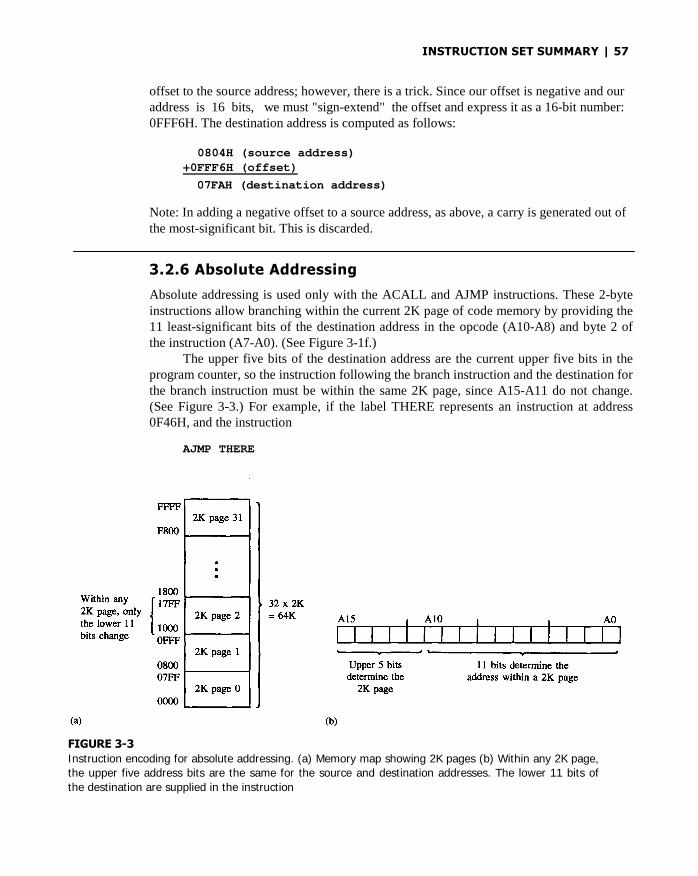
INSTRUCTION SET SUMMARY | 57
offset to the source address; however, there is a trick. Since our offset is negative and ouraddress is 16 bits, we must "sign-extend" the offset and express it as a 16-bit number:0FFF6H. The destination address is computed as follows:
0804H (source address)+0FFF6H (offset)
07FAH (destination address)
Note: In adding a negative offset to a source address, as above, a carry is generated out ofthe most-significant bit. This is discarded.
3.2.6 Absolute Addressing
Absolute addressing is used only with the ACALL and AJMP instructions. These 2-byteinstructions allow branching within the current 2K page of code memory by providing the11 least-significant bits of the destination address in the opcode (A10-A8) and byte 2 ofthe instruction (A7-A0). (See Figure 3-1f.)
The upper five bits of the destination address are the current upper five bits in theprogram counter, so the instruction following the branch instruction and the destination forthe branch instruction must be within the same 2K page, since A15-A11 do not change.(See Figure 3-3.) For example, if the label THERE represents an instruction at address0F46H, and the instruction
AJMP THERE
FIGURE 3-3
Instruction encoding for absolute addressing. (a) Memory map showing 2K pages (b) Within any 2K page,
the upper five address bits are the same for the source and destination addresses. The lower 11 bits of
the destination are supplied in the instruction

58 | CHAPTER 3
is in memory locations 0900H and 0901H, the assembler will encode the instruction as
11100001 - 1st byte (Al0-A8 + opcode)
01000110 - 2nd byte (A7-A0)
The underlined bits are the low-order 11 bits of the destination address, 0F46H =0000111101000110B. The upper five bits in the program counter will not change whenthis instruction executes. Note that both the AJMP instruction and the destination arewithin the 2K page bounded by 0800H and 0FFFH (see Figure 3-3), and therefore havethe upper five address bits in common.
Absolute addressing offers the advantage of short (2-byte) instructions, but has the dis-advantages of limiting the range for the destination and providing position-dependent code.
EXAMPLE An ACALL instruction is in memory locations 1024H and 1025H. The subroutine to3.8 which the call is directed begins in memory location 17A6H. What are the machine
language bytes for the ACALL instruction?
Solution
F1H, A6H
Discussion
As found in Appendix C, the encoding for the ACALL instruction is
aaal000l aaaaaaaa
The low-order 11 bits of the destination address are inserted into the instruction with bits10-8 placed in the high-order bits of the opcode and with bits 7-0 forming the second byteof the instruction. The destination address (17A6H) is shown below in binary with thelow-order 11 bits identified as a group of three bits (10-8) and a group of eight bits (7-F).
00010111 10100110 = 17A6H... aaa aaaaaaaa
The task is simply to correctly position the 11 bits from the destination address into the in-struction bytes. This positioning is illustrated as follows:
lll1000l 10100ll0 = 0F1A6H
aaa ............... aaaaaaaa
Note: Absolute addressing can only be used if the high-order five bits are the same in boththe source and destination addresses. It is this property that identifies the source and desti-nation addresses as falling within the same 2K page.
3.2.7 Long Addressing
Long addressing is used only with the LCALL and LJMP instructions. These 3-byte instructionsinclude a full 16-bit destination address as bytes 2 and 3 of the instruction. (See Figure 3-1g.)The advantage is that the full 64K code space may be used, but the disadvantage is that the
INSTRUCTION SET SUMMARY | 59
instructions are three bytes long and are position-dependent. Position-dependence is a dis-advantage because the program cannot execute at different addresses. If, for example, aprogram begins at 2000H and an instruction such as LJMP 2040H appears, then theprogram cannot be moved to, say, 4000H. The LJMP instruction would still jump to2040H, which is not the correct location after the program has been moved.
EXAMPLE What are the machine language bytes for the following instruction?
3.9 LJMP 8AF2H
Solution
02H, 8AH, F2H
Discussion
As given in Appendix C, the LJMP instruction is three bytes long with the opcode (02H) inthe first byte and the 16-bit destination address in bytes 2 and 3. The high byte of the des-tination address (8AH) is in byte 2, and the low byte (0F2H) is in byte 3.
3.2.8 Indexed Addressing
Indexed addressing uses a base register (either the program counter or the data pointer) andan offset (the accumulator) in forming the effective address for a JMP or MOVC instruc-tion. (See Figure 3-1h.) Jump tables or look-up tables are easily created using indexed ad-dressing. Examples are provided in Appendix C for the MOVC A,@A+<base-reg> andJMP @A+ DPTR instructions.
EXAMPLE What is the opcode for the following instruction?
3.10 MOVC A,@A+DPTR
Solution
93H
Discussion
The answer is found simply by looking up the MOVC instruction in Appendix C. The in-struction is only one byte long, with the opcode specifying both the operation and the ad-dressing mode. This instruction moves a byte of data from code memory to the accumulator.The address in code memory is found by adding the index (the present state of the accu-mulator) to the base register (the data pointer). When the instruction finishes executing, theindex is lost because it is overwritten with the value moved from code memory.
3.3 INSTRUCTION TYPES
The 8051 instructions are divided among five functional groups:
Arithmetic Logical Data transfer
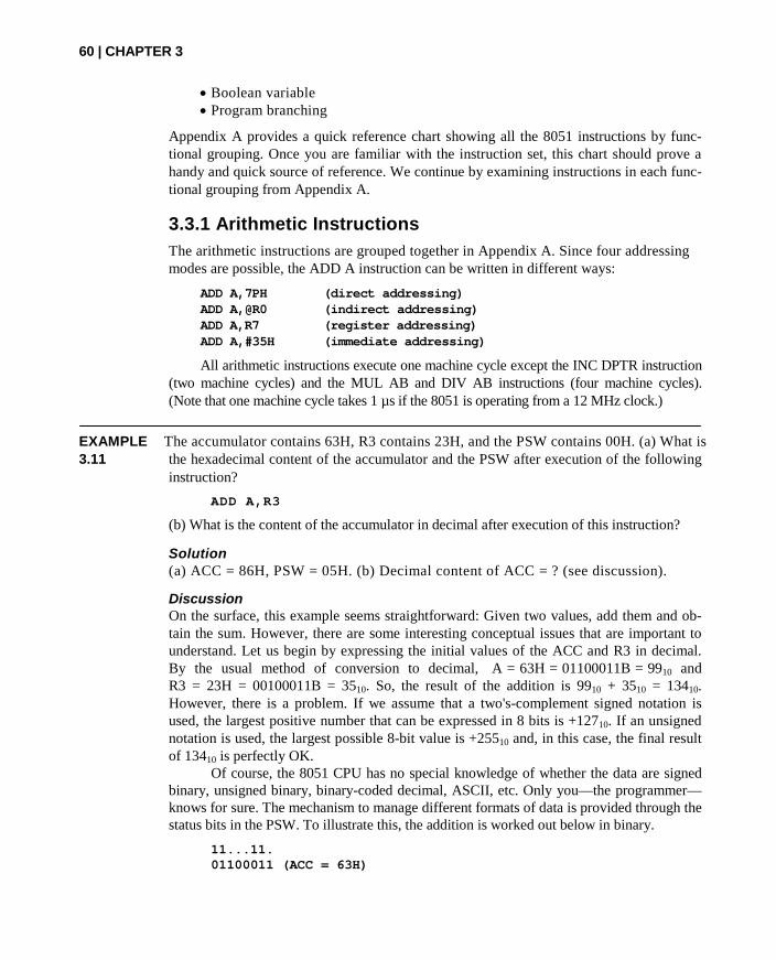
60 | CHAPTER 3
Boolean variable Program branching
Appendix A provides a quick reference chart showing all the 8051 instructions by func-tional grouping. Once you are familiar with the instruction set, this chart should prove ahandy and quick source of reference. We continue by examining instructions in each func-tional grouping from Appendix A.
3.3.1 Arithmetic Instructions
The arithmetic instructions are grouped together in Appendix A. Since four addressingmodes are possible, the ADD A instruction can be written in different ways:
ADD A,7PH (direct addressing)ADD A,@R0 (indirect addressing)ADD A,R7 (register addressing)ADD A,#35H (immediate addressing)
All arithmetic instructions execute one machine cycle except the INC DPTR instruction(two machine cycles) and the MUL AB and DIV AB instructions (four machine cycles).(Note that one machine cycle takes 1 µs if the 8051 is operating from a 12 MHz clock.)
EXAMPLE The accumulator contains 63H, R3 contains 23H, and the PSW contains 00H. (a) What is3.11 the hexadecimal content of the accumulator and the PSW after execution of the following
instruction?
ADD A,R3
(b) What is the content of the accumulator in decimal after execution of this instruction?
Solution(a) ACC = 86H, PSW = 05H. (b) Decimal content of ACC = ? (see discussion).
DiscussionOn the surface, this example seems straightforward: Given two values, add them and ob-tain the sum. However, there are some interesting conceptual issues that are important tounderstand. Let us begin by expressing the initial values of the ACC and R3 in decimal.By the usual method of conversion to decimal, A = 63H = 01100011B = 9910 andR3 = 23H = 00100011B = 3510. So, the result of the addition is 9910 + 3510 = 13410.However, there is a problem. If we assume that a two's-complement signed notation isused, the largest positive number that can be expressed in 8 bits is +12710. If an unsignednotation is used, the largest possible 8-bit value is +25510 and, in this case, the final resultof 13410 is perfectly OK.
Of course, the 8051 CPU has no special knowledge of whether the data are signedbinary, unsigned binary, binary-coded decimal, ASCII, etc. Only you—the programmer—knows for sure. The mechanism to manage different formats of data is provided through thestatus bits in the PSW. To illustrate this, the addition is worked out below in binary.
11...11.01100011 (ACC = 63H)
INSTRUCTION SET SUMMARY | 61
+00100011 (R3 = 23H)10000110 (result stored in ACC = 86H)
The result is 10000110B = 86H. Note above that carries occurred out of bits 0, 1, 5, and6. Carries did not occur out of bits 2, 3, 4, and 7. Because there was no carry out of bit 7,the C (carry) bit in the PSW is not set after the addition.
As for the OV (overflow) bit, the following description appears in Appendix C forthe ADD instruction: "the OV bit is set if there is a carry out of bit 6 but not out of bit 7,or a carry out of bit 7 but not out of bit 6; otherwise OV is cleared." This is a formal wayof saying, "the OV bit is set if the result is out of range for 8-bit signed numbers." In thisexample, there was a carry out of bit 6 but not out of bit 7; therefore, the OV bit is set.This makes sense if the data are signed, because the allowable range is -12810 to +12710
and the result of 9910 + 3510 is "out of range."
From the 8051 CPU's perspective, it is also possible that the data are binary-codeddecimal (only the programmer knows for sure!), and it will set or clear the auxiliary carrybit accordingly. Since a carry did not occur out of bit 3, the AC bit is cleared.
Finally, the P bit in the PSW is set or cleared to establish even parity with the accu-mulator. Because the result in the ACC has three bits equal to one, the P bit is set,bringing the total to four - an even number. The final value in the PSW is 00000101B =05H. Only the OV and P bits are set; the other bits are cleared (see Table 2-3).
The second question in this example is, "What is the content of the accumulator indecimal after execution of this instruction?" And it is here that we delve into the importantconcept of the meaning or interpretation of the data on which a CPU like the 8051 operates.Because the original problem did not indicate a format or representation for the original data,we cannot answer the question with certainty, hence the "?" in the solution. There are,however, at least two possible answers. First, if we assume the original data are in unsignedbinary notation, then the result is "in range" (because C = 0) and the answer is 13410. Sec-ond, if we assume the data are in signed binary notation using twos-complement notation,then the correct answer is "out of range" (because OV = 1). The important point is that themeaning or representation scheme in effect is not a characteristic of the CPU, but, rather, itis determined by the way the data are managed by the software.
EXAMPLE Illustrate an instruction sequence to subtract the content of R6 from R7 and leave the3.12 result in R7.
Solution
MOV A,R7CLR CSUBB A,R6MOV R7,A
Discussion
For both addition and subtraction, the accumulator holds one of the values for the operation.So, the first instruction above moves one of the bytes to the accumulator to prepare forthe operation. The second instruction clears the carry flag in the program status word. Thisis required because the only form of the subtract instruction is SUBB—subtract withborrow.
62 | CHAPTER 3
The operation subtracts from the accumulator the source byte and the carry bit. For subtractoperations, the carry bit serves as a "borrow" bit. If the state of the carry bit is unknown, itmust be explicitly cleared using CLR C before executing SUBB. The third instruction per-forms the subtraction, leaving the result in the accumulator. The fourth instruction movesthe result into R7.
The 8051 provides powerful addressing of its internal memory space. Any locationcan be incremented or decremented using direct addressing without going through the ac-cumulator. For example, if internal RAM location 7FH contains 40H, then the instruction
INC 7FH
increments this value, leaving 41H in location 7FH.
EXAMPLE Suppose the 8051 did not have an instruction to directly increment an internal RAM3.13 location. How could this operation be achieved?
Solution
MOVE A,directINC AMOV direct,A
Discussion
The first instruction moves a byte of data from an internal RAM location to the accumula-tor. The second instruction increments the value read (which is now in the accumulator),and the third instruction writes the result back to internal RAM. Not only is thisinstruction sequence longer and slower than the single-instruction equivalent (INC direct),the previous value of the accumulator is lost.
One of the INC instructions operates on the 16-bit data pointer. Since the datapointer generates 16-bit addresses for external memory, incrementing it in one operation isa useful feature. Unfortunately, a decrement data pointer instruction is not provided andrequires a sequence of instructions such as the following:
DEC DPL ;DECREMENT LOW-BYTE OF DPTRMOV R7,DPL ;MOVE TO R7CJNE R7,#0FFH,SKIP ;IF UNDERFLOOR TO FFDEC DPH ;DECREMENT HIGH-BYTE TOO
SKIP: (continue)
The high- and low-bytes of the DPTR must be decremented separately; however, the high-byte (DPH) is only decremented if the low-byte (DPL) underflows from 00H to 0FFH.
The MUL AB instruction multiplies the accumulator by the data in the B register andputs the 16-bit product into the concatenated B (high-byte) and accumulator (low-byte)registers. DIV AB divides the accumulator by the data in the B register, leaving the 8-bit

INSTRUCTION SET SUMMARY | 63
quotient in the accumulator and the 8-bit remainder in the B register. For example, if Acontains 25 (19H) and B contains 6 (06H), the instruction
DIV AB
divides the content of A by the content of B. The A accumulator is left with the value 4and the B accumulator is left with the value 1. (25 6 = 4 with a remainder of 1.)
EXAMPLE The accumulator contains 55H, the B register contains 22H, and the program status word3.14 contains 00H. What are the contents of these registers after execution of the following
instruction?
MUL AB
Solution
ACC = 4AH, B = 0BH, PSW = 05H
Discussion
You might be able to compute the answer using a calculator; otherwise begin by express-ing the original values in decimal: ACC = 55H = 8510 and B = 22H = 3410. The prod-uct is 8510 x 3410 = 2,89010 = 0B4AH. The high byte (0BH) is placed in register B andthe low byte (4AH) is placed in the accumulator. The P bit in the PSW is set to establisheven parity with the accumulator. Since the result is greater than 25510, the overflow flagis set, leaving the PSW containing 05H.
EXAMPLE The accumulator contains 1FH. What is the largest value that could be in register B such3.15 that the OV bit would not be set after executing the following instruction?
MUL AB
Solution
08H
Discussion
The accumulator contains 1FH = 3110. The overflow flag is set following MUL if the
product is greater than 25510. The largest number that 3110 can be multiplied by withoutthe product exceeding 25510 is 810 = 08H. (Note 3110 x 810 = 24810, 3110 x 910 =27910.)
For BCD (binary-coded decimal) arithmetic, ADD and ADDC must be followed bya DA A (decimal adjust) operation to ensure the result is in range for BCD. Note thatDAA will not convert a binary number to BCD; it produces a meaningful result only asthe second step in the addition of two BCD bytes. For example, if A contains the BCDvalue 59 (59H), then the instruction sequence
ADD A,#1DA A

64 | CHAPTER 3
first adds 1 to A, leaving the result 5AH, then adjusts the result to the correct BCD valueof 60 (60H). (59 + 1 = 60.)
EXAMPLE Illustrate how to add two 4-digit binary-coded decimal numbers. The first is in internal3.16 memory locations 40H and 41H, and the second is in locations 42H and 43H. The most-
significant digits are in locations 40H and 42H. Place the BCD result in locations 40H and41H.
Solution
MOV A,41HADD A,42HDA AMOV 42H,AMOV A,42HADDC A,40HDA A
MOV 40H,A
Discussion
This is an example of "multiprecision arithmetic," whereby a CPU is called upon to per-form arithmetic operations on data that are larger than the CPU's natural data size. Eventhough the 8051's arithmetic instructions operate on bytes, it is possible to add or subtractlarger data, for example, 16 bits or 32 bits. This is also true for binary-coded decimal num-bers. To add two 4-digit numbers, two byte additions are required.
The trick in multiprecision arithmetic is in propagating carries from byte to byte.During addition, carries are naturally propagated from bit to bit within a byte, but frombyte to byte, a carry—if it occurs—is temporarily held in the C bit in the PSW. Since acarry cannot occur into the low-order bytes, the first add instruction above is the generic"ADD." However, "ADDC" is required for the second add operation to include the carrythat may have occurred from the low-order byte. Both add instructions are followed byDA A to perform the necessary adjustment for binary-coded decimal values.
3.3.2 Logical Instructions
The 8051 logical instructions (see Appendix A) perform Boolean operations (AND, OR,Exclusive OR, and NOT) on bytes of data on a bit-by-bit basis. If the accumulatorcontains 00110101B, then the following AND logical instruction
ANL A,#01010011B
leaves the accumulator holding 00010001B. This is illustrated below.
01010022 (immediate data)AND 00220102 (original value of A)
00010002 (result in A)

INSTRUCTION SET SUMMARY | 65
Since the addressing modes for the logical instructions are the same as those forarithmetic instructions, the AND logical instruction can take several forms:
ANL A,55H (direct addressing)ANL A,@R0 (indirect addressing)ANL A,R6 (register addressing)ANL A,#33H (immediate addressing)
All logical instructions using the accumulator as one of the operands execute in onemachine cycle. The others take two machine cycles.
Logical operations can be performed on any byte in the internal data memory spacewithout going through the accumulator. The "XRL direct,#data" instruction offers a quickand easy way to invert port bits, as in
XRL P1,#0FFH
This instruction performs a read-modify-write operation. The eight bits at Port 1 are read;then each bit read is exclusive ORed with the corresponding bit in the immediate data.Since the eight bits of immediate data are all 1s, the effect is to complement each bit read
(e.g., A 1 = A ). The result is written back to Port 1.
The rotate instructions (RL A and RR A) shift the accumulator one bit to the left orright. For a left rotation, the MSB rolls into the LSB position. For a right rotation, the LSBrolls into the MSB position. The RLC A and RRC A variations are 9-bit rotates using theaccumulator and the carry flag in the PSW. If, for example, the carry flag contains 1 and Acontains 00H, then the instruction
RRC A
leaves the carry flag clear and A equal to 80H. The carry flag rotates into ACC.7 andACC.0 rotates into the carry flag.
The SWAP A instruction exchanges the high and low nibbles within theaccumulator. This is a useful operation in BCD manipulations. For example, if theaccumulator contains a binary number that is known to be less than 10010, it is quicklyconverted to BCD as follows:
MOV B,#10DIV ABSWAP AADD A,B
Dividing the number by 10 in the first two instructions leaves the tens digit in the low nib-ble of the accumulator, and the ones digit in the B register. The SWAP and ADD instruc-tions move the tens digit to the high nibble of the accumulator, and the ones digit to thelow nibble.
EXAMPLE Illustrate two ways to rotate the content of the accumulator three positions to the left3.17 Discuss the pros and cons of each method in terms of memory requirements and speed of
execution.

66 | CHAPTER 3
Solution(a) RL A
RL ARL A
(b) SWAP A
RR A
Discussion
Solution (a) is the most obvious approach, whereas solution (b) uses a trick. The SWAP Ainstruction swaps the low-order and high-order nibbles in the accumulator, and, as notedin Appendix C, this is equivalent to a 4-bit rotate operation. To undo the fourth rotation, afinal rotate to the right is used.
Although the effect of solutions (a) and (b) is the same, they are slightly different interms of memory usage and execution speed. All instructions above are 1-byte, 1-cycle in-structions (see Appendix C), so solution (a) uses three bytes of memory and takes threeCPU cycles to execute. Solution (b) uses only two bytes of memory and executes in twoCPU cycles. The difference may seem minuscule, but in the world of embedded controlsystems, squeezing every last ounce out of a program is often a design requirement.
EXAMPLE Write an instruction sequence to reverse the bits in the accumulator. Bit 7 and bit 0 are3.18 swapped, bit 6 and bit 1 are swapped, etc.
SolutionMOV R7,#8
LOOP: RLC A
XCH A,0F0H
RRC A
XCH A,0F0H
DJNZ R7,LOOP
XCH A,0F0H
Discussion
The gymnastics required in this example are sometimes called "dancing with bits." Thetask may seem contrived, but it is amazing how often situations arise that necessitatefiddling with the position of bits within bytes.
The approach taken in the solution is to build the new value in the B register by suc-cessively shifting a bit out of the accumulator into the carry bit and then shifting the samebit back into the B register. To reverse the bit pattern, the first shift is "to the left" and thesecond shift is "to the right." Because the rotate instruction only operates on the accumu-lator, the B register and the accumulator are exchanged (XCH) following each rotate. A fi-nal XCH positions the correct result in the accumulator. Note: The B register is at directaddress 0F0H.
3.3.3 Data Transfer Instructions
3.3.3.1 Internal RAM The instructions that move data within the internal memoryspaces (see Appendix A) execute in either one or two machine cycles. The instruction format
MOV <destination>, <source>
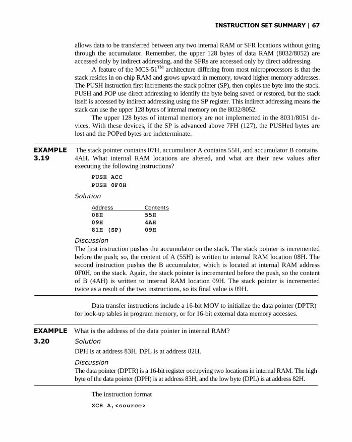
INSTRUCTION SET SUMMARY | 67
allows data to be transferred between any two internal RAM or SFR locations without goingthrough the accumulator. Remember, the upper 128 bytes of data RAM (8032/8052) areaccessed only by indirect addressing, and the SFRs are accessed only by direct addressing.
A feature of the MCS-51TM architecture differing from most microprocessors is that thestack resides in on-chip RAM and grows upward in memory, toward higher memory addresses.The PUSH instruction first increments the stack pointer (SP), then copies the byte into the stack.PUSH and POP use direct addressing to identify the byte being saved or restored, but the stackitself is accessed by indirect addressing using the SP register. This indirect addressing means thestack can use the upper 128 bytes of internal memory on the 8032/8052.
The upper 128 bytes of internal memory are not implemented in the 8031/8051 de-vices. With these devices, if the SP is advanced above 7FH (127), the PUSHed bytes arelost and the POPed bytes are indeterminate.
EXAMPLE The stack pointer contains 07H, accumulator A contains 55H, and accumulator B contains3.19 4AH. What internal RAM locations are altered, and what are their new values after
executing the following instructions?
PUSH ACC
PUSH 0F0H
Solution
Address Contents
08H 55H09H 4AH81H (SP) 09H
Discussion
The first instruction pushes the accumulator on the stack. The stack pointer is incrementedbefore the push; so, the content of A (55H) is written to internal RAM location 08H. Thesecond instruction pushes the B accumulator, which is located at internal RAM address0F0H, on the stack. Again, the stack pointer is incremented before the push, so the contentof B (4AH) is written to internal RAM location 09H. The stack pointer is incrementedtwice as a result of the two instructions, so its final value is 09H.
Data transfer instructions include a 16-bit MOV to initialize the data pointer (DPTR)for look-up tables in program memory, or for 16-bit external data memory accesses.
EXAMPLE What is the address of the data pointer in internal RAM?
3.20 Solution
DPH is at address 83H. DPL is at address 82H.
Discussion
The data pointer (DPTR) is a 16-bit register occupying two locations in internal RAM. The highbyte of the data pointer (DPH) is at address 83H, and the low byte (DPL) is at address 82H.
The instruction format
XCH A,<source>
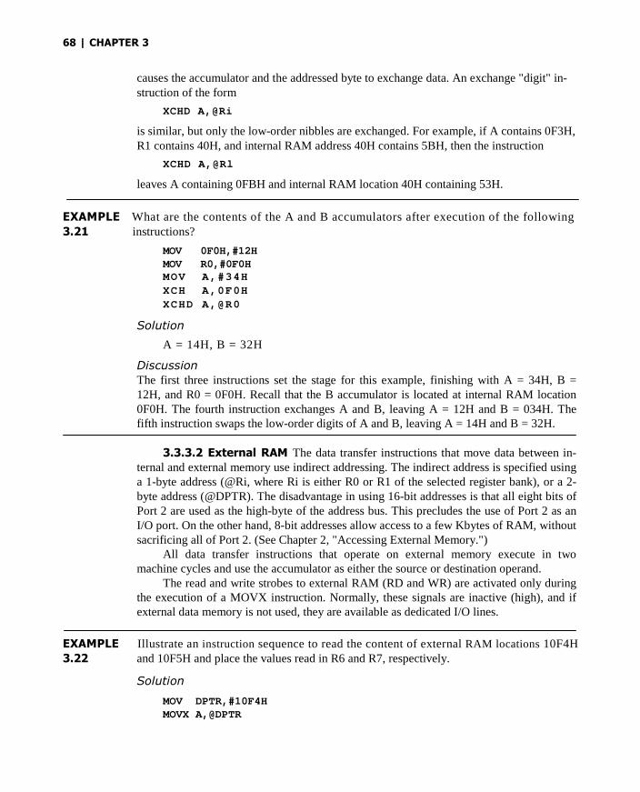
68 | CHAPTER 3
causes the accumulator and the addressed byte to exchange data. An exchange "digit" in-struction of the form
XCHD A,@Ri
is similar, but only the low-order nibbles are exchanged. For example, if A contains 0F3H,R1 contains 40H, and internal RAM address 40H contains 5BH, then the instruction
XCHD A,@Rl
leaves A containing 0FBH and internal RAM location 40H containing 53H.
EXAMPLE What are the contents of the A and B accumulators after execution of the following3.21 instructions?
MOV 0F0H,#12HMOV R0,#0F0HMOV A,#34H
XCH A,0F0H
XCHD A,@R0
Solution
A = 14H, B = 32H
Discussion
The first three instructions set the stage for this example, finishing with A = 34H, B =12H, and R0 = 0F0H. Recall that the B accumulator is located at internal RAM location0F0H. The fourth instruction exchanges A and B, leaving A = 12H and B = 034H. Thefifth instruction swaps the low-order digits of A and B, leaving A = 14H and B = 32H.
3.3.3.2 External RAM The data transfer instructions that move data between in-ternal and external memory use indirect addressing. The indirect address is specified usinga 1-byte address (@Ri, where Ri is either R0 or R1 of the selected register bank), or a 2-byte address (@DPTR). The disadvantage in using 16-bit addresses is that all eight bits ofPort 2 are used as the high-byte of the address bus. This precludes the use of Port 2 as anI/O port. On the other hand, 8-bit addresses allow access to a few Kbytes of RAM, withoutsacrificing all of Port 2. (See Chapter 2, "Accessing External Memory.")
All data transfer instructions that operate on external memory execute in twomachine cycles and use the accumulator as either the source or destination operand.
The read and write strobes to external RAM (RD and WR) are activated only duringthe execution of a MOVX instruction. Normally, these signals are inactive (high), and ifexternal data memory is not used, they are available as dedicated I/O lines.
EXAMPLE Illustrate an instruction sequence to read the content of external RAM locations 10F4H3.22 and 10F5H and place the values read in R6 and R7, respectively.
Solution
MOV DPTR,#10F4HMOVX A,@DPTR

INSTRUCTION SET SUMMARY | 69
MOV R6,AINC DPTRMOVX A,@DPTRMOV R7,A
DiscussionThe first instruction initializes the data pointer with the first of the two external addresses to beread. The second instruction reads a byte from external memory location 10F4H and places it inthe accumulator. The third instruction transfers the byte read to register 6. Note that the MOVXinstruction must use the accumulator as either the source or destination of data. The fourth in-struction increments the data pointer, leaving it pointing to the second of the two external ad-dresses to be read. The fifth instruction reads a byte from external memory location 10F4H andplaces it in the accumulator. The sixth instruction transfers the byte read to register 7.
3.3.3.3 Look-Up Tables Two data transfer instructions are available for reading look-up tables in program memory. Since they access program memory, the look-up tables can onlybe read, not updated. The mnemonic is MOVC for "move constant." MOVC uses either theprogram counter or the data pointer as the base register and the accumulator as the offset.
The instruction
MOVC A,@A+DPTR
can accommodate a table of 246 entries, numbered 0 through 255. The number of the de-sired entry is loaded into the accumulator and the data pointer is initialized to thebeginning of the table. The instruction
MOVC A,@A+PC
works the same way, except the program counter is the base address. The table is usually ac-cessed through a subroutine. First, the number of the desired entry is loaded into the accumu-lator, and then the subroutine is called. The setup and call sequence would be coded as follows:
MOV A,#ENTRY_NUMBERCALL LOOKUP
.
.
.LOOKUP: INC A
MOVC A,@A+PCRET
TABLE: DB data, data, data, data, ...
The table immediately follows the RET instruction in program memory. The INC instruc-tion is needed because the PC points to the RET instruction when MOVC executes. Incre-menting the accumulator will effectively bypass the RET instruction when the table look-uptakes place.
Note however that even though we would expect to get a table of 256 entries whenusing this technique, we only get 255 entries in this case since we lose one entry due to theeffect of the INC A instruction. Consider the entry number of 255 that is moved into the ac-cumulator. The INC A instruction increments it by 1, causing the value 255 to recycle back

70 | CHAPTER 3
to 0 since the accumulator is 8 bits in size. The next instruction, MOVC A,@A+PC, wouldattempt to load the accumulator with the value of RET, which is invalid. Therefore, validentries are only from 0 to 254.
EXAMPLE Write a subroutine called SQUARE to compute the square of an integer between 0 and3.23 9. Enter the subroutine with the integer in A,and return with the square of the integer in A.
Write two versions of the subroutine: (a) using a look-up table, and (b) without using alookup table. Then (c) illustrate a call sequence to convert 6 to its square, 36.
Solution
a. Using a look-up table:
SQUARE: INC A
MOVC A,@A+PCRET
TABLE: DB 0,1,4,9,16,25,36,49,64,81
b. Without using a look-up table:
SQUARE: PUSH 0F0HMOV 0F0H,AMUL ABPOP 0F0HRET
c. Call sequence:
MOV A,#6CALL SQUARE
Discussion
The solution in (a) and the call sequence in (c) are straightforward implementations of a lookuptable in program memory. For this example, however, there is an interesting alternative ap-proach, as shown in (b). By copying the content of A to the B accumulator (in internal RAMlocation 0FFH), and then multiplying B times A using MUL AB, the square is computed andleft in A. Since the B accumulator is overwritten by the second instruction, it is first saved onthe stack and then restored from the stack before returning from the subroutine. ThePUSH/POP instructions may not be needed, depending on the context; however, it is goodprogramming practice to design subroutines to have as few side effects as possible.
In comparing solutions (a) and (b), we find an interesting tradeoff. Solution (a) is 13bytes, including the look-up table, whereas solution (b) is only eight bytes. However, so-lution (a) executes in five CPU cycles, whereas solution (b) executes in 11 cycles. Thetradeoff is that solution (a) is faster (which is good!) but consumes more memory (whichis bad!), compared with solution (b), which is slower (which is bad!) but consumes lessmemory (which is good!). This tradeoff would be more pronounced if the look-up tablewas large, because every entry adds one byte to the size of the routine.
In many situations, the relationship between the index to a table and the entrieswithin a table is not as simple as in this example, and using a look-up table is the onlyviable implementation.
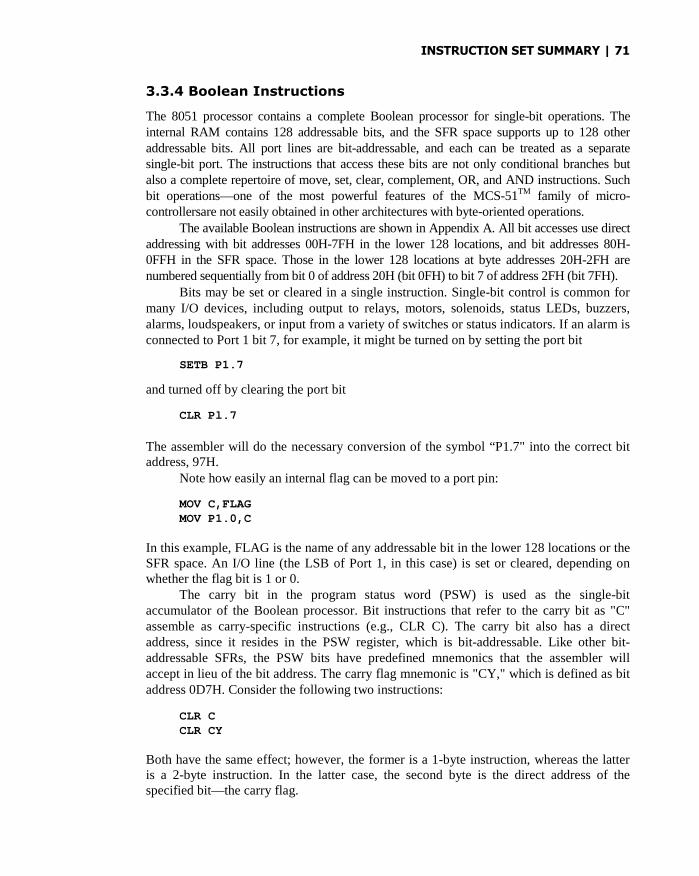
INSTRUCTION SET SUMMARY | 71
3.3.4 Boolean Instructions
The 8051 processor contains a complete Boolean processor for single-bit operations. Theinternal RAM contains 128 addressable bits, and the SFR space supports up to 128 otheraddressable bits. All port lines are bit-addressable, and each can be treated as a separatesingle-bit port. The instructions that access these bits are not only conditional branches butalso a complete repertoire of move, set, clear, complement, OR, and AND instructions. Suchbit operations—one of the most powerful features of the MCS-51TM family of micro-controllersare not easily obtained in other architectures with byte-oriented operations.
The available Boolean instructions are shown in Appendix A. All bit accesses use directaddressing with bit addresses 00H-7FH in the lower 128 locations, and bit addresses 80H-0FFH in the SFR space. Those in the lower 128 locations at byte addresses 20H-2FH arenumbered sequentially from bit 0 of address 20H (bit 0FH) to bit 7 of address 2FH (bit 7FH).
Bits may be set or cleared in a single instruction. Single-bit control is common formany I/O devices, including output to relays, motors, solenoids, status LEDs, buzzers,alarms, loudspeakers, or input from a variety of switches or status indicators. If an alarm isconnected to Port 1 bit 7, for example, it might be turned on by setting the port bit
SETB P1.7
and turned off by clearing the port bit
CLR Pl.7
The assembler will do the necessary conversion of the symbol “P1.7" into the correct bitaddress, 97H.
Note how easily an internal flag can be moved to a port pin:
MOV C,FLAGMOV P1.0,C
In this example, FLAG is the name of any addressable bit in the lower 128 locations or theSFR space. An I/O line (the LSB of Port 1, in this case) is set or cleared, depending onwhether the flag bit is 1 or 0.
The carry bit in the program status word (PSW) is used as the single-bitaccumulator of the Boolean processor. Bit instructions that refer to the carry bit as "C"assemble as carry-specific instructions (e.g., CLR C). The carry bit also has a directaddress, since it resides in the PSW register, which is bit-addressable. Like other bit-addressable SFRs, the PSW bits have predefined mnemonics that the assembler willaccept in lieu of the bit address. The carry flag mnemonic is "CY," which is defined as bitaddress 0D7H. Consider the following two instructions:
CLR CCLR CY
Both have the same effect; however, the former is a 1-byte instruction, whereas the latteris a 2-byte instruction. In the latter case, the second byte is the direct address of thespecified bit—the carry flag.
72 | CHAPTER 3
Logical operations such as AND, OR, NAND, NOR, and NOT are easy toimplement for single-bit variables. Furthermore, the variables may be input or outputsignals on the 8051's I/O ports. Thus, the state of an I/O pin may be directly read or writtenaccompanied by a Boolean operation. Suppose one wanted to compute the logical AND ofthe input signals on bit 0 and bit 1 of Port 1 and output the result to bit 2 of Port 1. Thislogical relationship is illustrated in Figure 3-4.
The following instruction sequence creates this logical operation:
LOOP: MOV C,P1.0 ;n1 = 1 cycle
ANL C,P1.1 ;n2 = 2 cycles
MOV P1.2,C ;n3 = 2 cycles
SJMP LOOP ;n4 = 2 cycles
Bits P1.0 and P1.1 are continuously read with the logical AND of the result continuouslypresented on P1.2.
If the logic operation in Figure 3-4 is implemented using a typical electronic logiccircuit, such as a 74AL508, then the input-to-output propagation delay is on the order of 7ns. This is the time from an input signal transition to the correct logic level appearing atthe output. What is the worst-case propagation delay for the circuit in Figure 3-4 if imple-mented using the software above? Figure 3-5 will assist in answering this question. Theworst-case scenario is that P1.0 changes just after the first instruction, shown at "A" in thefigure. The change is not sensed until the next pass through the loop. The correct outputstate appears at "B" in the figure. The solid line in Figure 3-5 illustrates the sequence of in-structions for the worst-case scenario. The number of CPU cycles from "A" to "B," fol-lowing the solid line, is 11. At 12 MHz operation the worst-case delay is 11 µs. Obviouslythere is "no contest" in comparing the speed of a microcontroller with speed of electroniclogic circuits. The software implementation for Figure 3-4 is about a thousand timesslower than a 74LS08 AND gate!
Note that the Boolean instructions include ANL (AND logical) and ORL (OR logical)operations, but not the XRL (exclusive OR logical) operation. An XRL operation is simple
FIGURE 3-4
Simple implementation of a logical
AND operation
FIGURE 3-5
Instruction sequence for worst-
case propagation delay

INSTRUCTION SET SUMMARY | 73
to implement. Suppose, for example, it is required to form the exclusive OR of two bits,BIT1 and BIT2, and leave the result in the carry flag. The instructions are shown below.
MOV BIT1JNB BIT2,SKIPCPL C
SKIP: (continue)
First, BIT1 is moved to the carry flag. If BIT2 = 0, then C contains the correct re-sult; that is, BIT1 BIT2 = BIT1 if BIT2 = 0. If BIT2 = 1, C contains the complement ofthe correct result. Complementing C completes the operation.
3.3.4.1 Bit Testing The code in the example above uses the JNB instruction, oneof a series of bit-test instructions that jump if the addressed bit is set (JC, JB, JBC) or if theaddressed bit is not set (JNC, JNB). In the above case, if BIT2 = 0 the CPL instruction isskipped. JBC (jump if bit set then clear bit) executes the jump if the addressed bit is set,and also clears the bit; thus, a flag can be tested and cleared in a single instruction.
All PSW bits are directly addressable, so the parity bit or the general purpose flags,for example, are also available for bit-test instructions.
3.3.5 Program Branching Instructions
As evident in Appendix A, there are numerous instructions to control the flow ofprograms, including those that call and return from subroutines or branch conditionally orunconditionally. These possibilities are enhanced further by the three addressing modes forthe program branching instructions.
There are three variations of the JMP instruction: SJMP, LJMP, and AJMP (usingrelative, long, and absolute addressing, respectively). Intel's assembler (ASM51) allowsthe use of the generic JMP mnemonic if the programmer does not care which variation isencoded. Assemblers from other companies may not offer this feature. The generic JMPassembles to AJMP if the destination contains no forward reference and is within the same2K page (as the instruction following the AJMP). Otherwise, it assembles to LJMP. Thegeneneric CALL instruction (see below) works the same way.
The SJMP instruction specifies the destination address as a relative offset, as shownin the earlier discussion on addressing modes. Since the instruction is two bytes long (anopcode plus a relative offset), the jump distance is limited to -128 to +127 bytes relative tothe address following the SJMP.
The LJMP instruction specifies the destination address as a 16-bit constant. Sincethe instruction is three bytes long (an opcode plus two address bytes), the destinationaddress can be anywhere in the 64K program memory space.
The AJMP instruction specifies the destination address as an 11-bit constant. As withSJMP, this instruction is two bytes long, but the encoding is different. The opeode containsthree of the 11 address bits, and byte 2 holds the low-order eight bits of the destination ad-dress. When the instruction is executed, these 11 bits replace the low-order 11 bits in thePC, and the high-order five bits in the PC stay the same. The destination, therefore, mustbe within the same 2K block as the instruction following the AJMP. Since there is 64K of

74 | CHAPTER 3
code memory space, there are 32 such blocks, each beginning at a 2K address boundary(0000H, 0800H, 1000H, 1800H, etc., up to 0F800H; see Figure 3-3).
In all cases the programmer specifies the destination address to the assembler in theusual way - as a label or as a 16-bit constant. The assembler will put the destinationaddress into the correct format for the given instruction. If the format required by theinstruction will not support the distance to the specified destination address, a "destinationout of range" message is given.
3.3.5.1 Jump Tables The JMP @A+DPTR instruction supports case-dependentjumps for jump tables. The destination address is computed at execution time as the sumof the 16-bit DPTR register and the accumulator. Typically the DPTR is loaded with theaddress of a jump table, and the accumulator acts as an index. If, for example, five "cases"are desired, a value from 0 through 4 is loaded into the accumulator and a jump to theappropriate case is performed as follows:
MOV DPTR,#JUMP_TABLEMOV A,#INDEX_NUMBERRL AJMP @A+DPTR
The RL A instruction above converts the index number (0 through 4) to an even number inthe range 0 through 8 because each entry in the jump table is a 2-byte address:
JUMP_TABLE: AJMP CASE0AJMP CASE1AJMP CASE2AJMP CASE3
EXAMPLE Suppose the jump table above begins at code memory location 8100H with the following3.24 memory assignments:
Address Content8100 0l810l B88102 0l8103 438104 418105 768106 El
8107 F0
a. What is the beginning and ending address of the 2K block of code memory withinwhich these instructions reside?
b. At what addresses do CASE0 through CASE3 begin?
Solution
a. 8000H to 87FFH
b. CASE0 begins at address 80B8HCASE1 begins at address 8043H
INSTRUCTION SET SUMMARY | 75
CASE2 begins at address 8276HCASE3 begins at address 87F0H
Discussion
This example has more to do with absolute addressing than with jump tables. The jumptable consists of a series of four ACALL instructions. Since this instruction uses absoluteaddressing, the jump destinations must be within the same 2K page as the ACALLinstructions. A 2K page is a block of code memory with the upper five address bits thesame. The upper five bits in 8100H are 1000B. The other 11 address bits for each CASEroutine consist of the upper three bits in the ACALL opcode and the second byte of theACALL instruction. Consider ACALL CASE3, which is located in locations 8106H (21H)and 8107H (0F0H). The upper three bits of the opcode are 111B and the second byte of theinstruction is 11110000B. Concatenating the three binary patterns in the order just givenyields 10000111 11110000B = 87F0H, the address of the CASE3 routine.
3.3.5.2 Subroutines and Interrupts There are two variations of the CALL in-struction: ACALL and LCALL, using absolute and long addressing, respectively. As withJMP, the generic CALL mnemonic may be used with Intel's assembler if the programmerdoes not care which way the address is encoded. Either instruction pushes the content of theprogram counter on the stack and loads the program counter with the address specified in theinstruction. Note that the PC will contain the address of the instruction following the CALLinstruction when it gets pushed on the stack. The PC is pushed on the stack low-byte first,high-byte second. The bytes are popped from the stack in the reverse order. For example, ifan LCALL instruction is in code memory at locations 1000H-1002H and the SP contains20H, then LCALL (a) pushes the return address (1003H) on the internal stack, placing 03Hin 21H and 10H in 22H; (b) leaves the SP containing 22H; and (c) jumps to the subroutine byloading the PC with the address contained in bytes 2 and 3 of the instruction.
EXAMPLE The following instruction
3.25 LCALL COSINE
is in code memory at addresses 0204H through 0206H, and the subroutine COSINEbegins at code memory address 043AH. Assume the stack pointer contains 3AH justbefore this instruction executes. What internal RAM locations are altered, and what aretheir new values after execution of the LCALL instruction?
Solution
Address Contents3BH 07H3CH 02H81H (SP) 3CH
Discussion
Since the LCALL instruction is three bytes long, the instruction following it is at code mem-ory location 0207H. This is the address to which the program must return at the end of thesubroutine, and it is the address that is saved on the stack before branching to the subroutine.

76 | CHAPTER 3
Since the stack pointer contains 3AH initially, and, since it is incremented before writingto the stack, the low byte of the return address (02H) is saved at internal memory location3BH, and the high byte of the return address (02H) is saved at internal memory location3CH. Since two bytes are saved on the stack, the SP is incremented twice and contains3CH after the LCALL instruction executes. Note that the stack pointer is a specialfunction register located at internal RAM address 81H.
The LCALL and ACALL instructions have the same restrictions on the destinationaddress as the LJMP and AJMP instructions just discussed.
Subroutines should end with an RET instruction, which returns execution to the in-struction following the CALL. There is nothing magical about the way the RETinstruction gets back to the main program. It simply "pops" the last two bytes off the stackand places them in the program counter. It is a cardinal rule of programming withsubroutines that they should always be entered with a CALL instruction, and they shouldalways be exited with a RET instruction. Jumping in or out of a subroutine any other wayusually fouls up the stack and causes the program to crash.
RETI is used to return from an interrupt service routine (ISR). The only differencebetween RET and RETI is that RETI signals the interrupt control system that the interruptin progress is done. If there is no interrupt pending at the time RETI is executed, thenRETI is functionally identical to RET. Interrupts and the RETI instruction are discussed inmore detail in Chapter 6.
EXAMPLE The stack pointer contains 1CH just prior to the execution of3.26
RET
at the end of a subroutine. What is the value of the stack pointer after execution of this in-
struction?
Solution
1CH
Discussion
The return address for the subroutine is 16 bits or two bytes. The purpose of the RET in-struction is to retrieve two bytes from the stack and place them in the program counter,thus allowing the program to continue executing at the location following the callinstruction that leads to the subroutine. Regardless of what address this may be, the stackpointer contains two less than its value before RET executed.
EXAMPLE XORing Bits3.27 The 8051 instruction set does not include an instruction to XOR two bit values. Write a
subroutine XRB that effectively behaves as an instruction to XOR two bits in the formXRB C, P. This means that the two bit values are stored in C and P, respectively, prior tothe calling of the subroutine, and the XORed result should be put back in C.
INSTRUCTION SET SUMMARY | 77
Solution
XRB: MOV 20H,C ;backup the first bit, x
ANL C,/P ;C = x y
MOV 21H,C ;backup partial result, x y
MOV C,P ;put second bit, y in C
ANL C,/20H ;C = y x
ORL C,21H ;C = y x + x y
Discussion
There are three approaches to solve this problem. In this example, we use the fact thatxy = x y + y x. The other two cases are left as an exercise for the reader in the prob-lems section:
Change each bit into a byte and then do XOR on the bytes Use JB and JNB.
3.3.5.3 Conditional Jumps The 8051 offers a variety of conditional jump in-structions. All of these specify the destination address using relative addressing and so arelimited to a jump distance of -128 to +127 bytes from the instruction following the con-ditional jump instruction. Note, however, that the user specifies the destination address thesame way as with the other jumps, as a label or 16-bit constant. The assembler does the rest.
There is no 0-bit in the PSW. The JZ and JNZ instructions test the accumulator datafor that condition.
The DJNZ instruction (decrement and jump if not zero) is for loop control. To exe-cute a loop N times, load a counter byte with N and terminate the loop with a DJNZ to thebeginning of the loop, as shown below for N = 10.
MOV R7,#10
LOOP: (begin loop)
.
.
.(end loop)DJNZ R7,LOOP(continue)
The CJNE instruction (compare and jump if not equal) is also used for loop control.Two bytes are specified in the operand field of the instruction, and the jump is executedonly if the two bytes are not equal. If, for example, a character has just been read into theaccumulator from the serial port and it is desired to jump to an instruction identified by thelabel TERMINATE if the character is CONTROL-C (03H), then the following instructionscould be used:
CJNE A,#03H,SKIPSJMP TERMINATE
SKIP: (continue)
78 | CHAPTER 3
Since the jump occurs only if A CONTROL-C, a skip is used to bypass the terminatingjump instruction except when the desired code is read.
Another application of this instruction is in "greater than" or "less than" comparisons.The two bytes in the operand field are taken as unsigned integers. If the first is less thanthe second, the carry flag is set. If the first is greater than or equal to the second, the carryflag is cleared. For example, if it is desired to jump to BIG if the value in the accumulatoris greater than or equal to 20H, the following instructions could be used:
CJNE A,#20H,$+3JNC BIG
The jump destination for CJNE is specified as "$+3." The dollar sign ($) is a specialassembler symbol representing the address of the current instruction. Since CJNE is a 3-byteinstruction, "$+3" is the address of the next instruction, JNC. In other words, the CJNE in-struction follows through to the JNC instruction regardless of the result of the compare. Thesole purpose of the compare is to set or clear the carry flag. The JNC instruction decideswhether or not the jump takes place. This example is one instance in which the 8051 approachto a common programming situation is more awkward than with most microprocessors; how-ever, as we shall see in Chapter 7, the use of macros allows powerful instruction sequences,such as the example above, to be constructed and executed using a single mnemonic.
SUMMARY
This chapter has presented the 8051 instruction set. The reader is encouraged to refer toAppendix C for more examples of using this instruction set. 0f course, nothing beats prac-tice so the reader should really try out as many programming examples as possible. Thenext three chapters will discuss more programming examples in terms of interacting withthe 8051's on-chip peripherals: the timers, the serial port, and the interrupts.
PROBLEMS
3.1 What are the hexadecimal bytes for the following instructions?a. INC DPTR
b. MOV A,#-2
c. MOVX @DPTR,A
d. CJNE A,#0DH,$+3
e. PUSH ACC
f. SETB P2.2
3.2 What are the hexadecimal bytes for the following instructions?a. MOV DPH,#84H
b. JNB ACC.0,$
c. POP DPH
d. MOV A,#'='

INSTRUCTION SET SUMMARY | 79
e. XLR A,#'S'
f. CLR C
3.3 What instructions are represented by the following machine language bytes?a. 07EH, 002H
b. 0C2H, 097H
c. 013H
d. 0F6H
e. 022H
f. 090H, 080H, 030H
3.4 What instructions are represented by the following machine language bytes?a. 0EFH
b. 012H, 080H, 050H
c. 0F5H, 08DH
d. 004H
e. 083H
f. 075H, 0BAH, 0E7H
3.5 List all the 8051's 3-byte instructions with an opcode ending in 5H.3.6 List all the 8031's 2-byte instructions beginning with 2H.3.7 Illustrate how the content of internal address 50H could be transferred to the
accumulator, using indirect addressing.3.8 Illustrate two ways to transfer the content of the accumulator to internal RAM
address 3CH.3.9 What opcode is undefined on the 8051?3.10 How many opcodes are defined on the 8052?3.11 The following is an 8051 instruction:
MOV 50H,#0FFH
a. What is the opcode for this instruction?b. How many bytes long is this instruction?c. Explain the purpose of each byte of this instruction.d. How many machine cycles are required to execute this instruction?e. If an 8051 is operating from a 16 MHz crystal, how long does this instruction
take to execute?
3.12 The following is an 8051 instruction:
CJNE A,#'Q',AHEAD
a. What is the opcode for this instruction?b. How many bytes long is this instruction?c. Explain the purpose of each byte of this instruction.d. How many machine cycles are required to execute this instruction?e. If an 8051 is operating from a 10 MHz crystal, how long does this instruction
take to execute?
3.13 What is the relative offset for the instruction
SJMP AHEAD
if the instruction is in locations 0400H and 0401H, and the label AHEADrepresents the instruction at address 041FH?

INSTRUCTION SET SUMMARY | 81
(a) (b) (c)
FIGURE 3-6
Logic gate programming problems. (a) 3-input NOR. (b) 8-input NAND. (c) 3-gate logic operation.
3.26 Assume the PSW contains 0C0H and accumulator A contains 40H just before thefollowing instruction executes:
RLC A
What is the content of accumulator A after this instruction executes?3.27 Assume the PSW contains 78H and the accumulator contains 81H. What is the con-
tent of the accumulator after the following instruction executes?
RRC A
3.28 What instruction sequence could be used to create a 5 µs low-going pulse on P1.7?Assume P1.7 is high initially and the 8041 is operating from a 12 MHz crystal.
3.29 Write a program to create an 83.3 kHz square wave on P1.0. (Assume 12 MHzoperation.)
3.30 Write a program to generate a 4 µs active-high pulse on P1.7 every 200 µs.3.31 Write programs to implement the logic operations shown in Figure 3-6. For each
program, what is the worst-case propagation delay from an input transition to anout-put transition? Assume 12 MHz operation.
3.32 Write programs to implement the logic operations shown in Figure 3-7. For eachprogram, what is the worst-case propagation delay from an input transition to anoutput transition? Assume 12 MHz operation.
3.33 What is the content of accumulator A after the following instruction sequenceexecutes?
MOV A,#7FH
MOV 50H,#29H
FIGURE 3-7
Logic gate programming problems. (a) 2-gate logic circuit. (b) 3-gate logic circuit.(c) 4-input NOR.

80 | CHAPTER 3
SJMP BACK
if the instruction is in locations 0A051H and 0A041H, and the label BACKrepresents the instruction at address 9FE0H?
3.15 Assume the instructionAJMP AHEAD
is in code memory at addresses 2FF0H and 2FF1H, and the label AHEAD correspondsto an instruction at address 2F96H. What are the hexadecimal machine language bytesfor this instruction?
3.16 Assume the instructionACALL FACTORIAL
is in code memory at locations 06F5H and 06F5H, and the label FACTORIALcorresponds to a subroutine beginning at address 07ABH. What are the machinelanguage bytes for this instruction?
3.17 At a certain point in a program, it is desired to jump to the label EXIT if theaccumulator equals the carriage return ASCII code. What instruction(s) would beused?
3.18 At a certain point in a program, it is desired to jump to the label EXIT if theaccumulator equals the ASCII code for 'Q' or 'q,' or continue on otherwise. Whatinstruction(s) would be used?
3.19 The instructionSJMP BACK
is in code memory at address 0100H and 0101H and the label BACK corresponds toan instruction at address 00AEH. What are the hexadecimal machine language bytesfor this instruction?
3.20 The instructionCJNE R7,#'Z',NOTZED
is in code memory at addresses 022AH through 022CH. What are the machinelanguage bytes for this instruction?
3.21 What does the following instruction do?SETH 0D7H
What is a better way to perform the same operation? Why?3.22 What is the difference between the following two instructions?
INC A
INC ACC
3.23 What are the machine language bytes for the instruction
LJMP ONWARD
if the label ONWARD represents the instruction at address 0A0F6H?3.24 Assume accumulator A contains 4AH. What is the result in accumulator A after the
following instruction executes?XRL A,#0FFH
3.25 Assume the accumulator contains 29H. What is the content of the accumulator afterthe following instruction executes?
ORL A,#47H
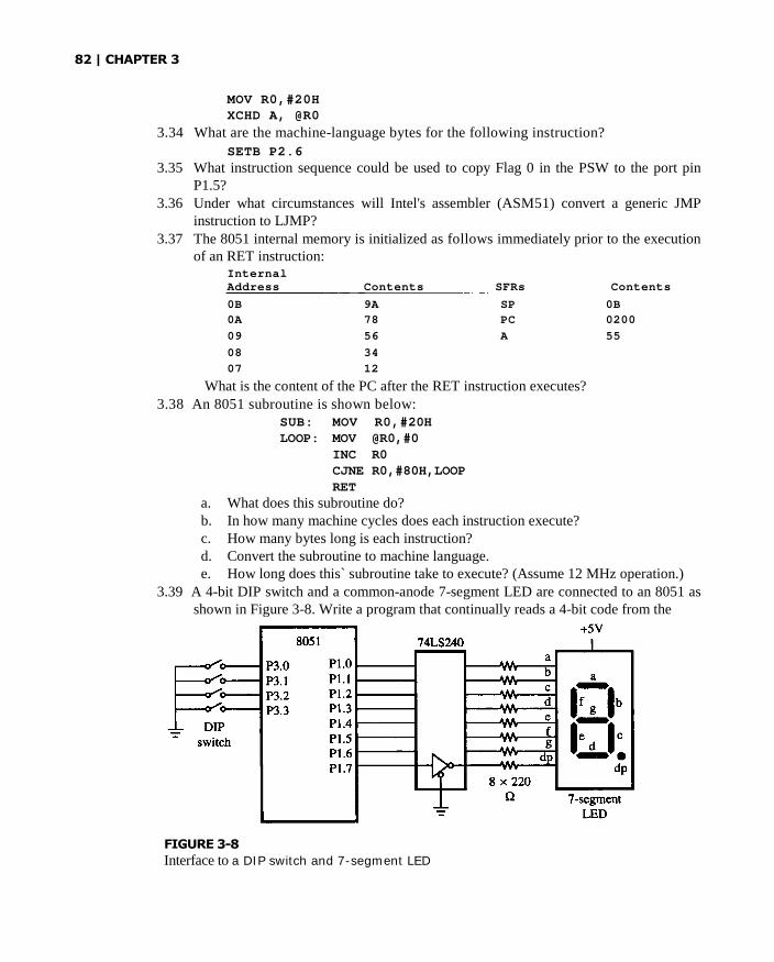
82 | CHAPTER 3
MOV R0,#20HXCHD A, @R0
3.34 What are the machine-language bytes for the following instruction?
SETB P2.6
3.35 What instruction sequence could be used to copy Flag 0 in the PSW to the port pinP1.5?
3.36 Under what circumstances will Intel's assembler (ASM51) convert a generic JMPinstruction to LJMP?
3.37 The 8051 internal memory is initialized as follows immediately prior to the executionof an RET instruction:
InternalAddress Contents SFRs Contents
0B 9A SP 0B
0A 78 PC 0200
09 56 A 55
08 34
07 12
What is the content of the PC after the RET instruction executes?3.38 An 8051 subroutine is shown below:
SUB: MOV R0,#20HLOOP: MOV @R0,#0
INC R0CJNE R0,#80H,LOOPRET
a. What does this subroutine do?b. In how many machine cycles does each instruction execute?c. How many bytes long is each instruction?d. Convert the subroutine to machine language.e. How long does this` subroutine take to execute? (Assume 12 MHz operation.)
3.39 A 4-bit DIP switch and a common-anode 7-segment LED are connected to an 8051 asshown in Figure 3-8. Write a program that continually reads a 4-bit code from the
FIGURE 3-8
Interface to a DIP switch and 7-segment LED

INSTRUCTION SET SUMMARY | 83
DIP switch and updates the LEDs to display the appropriate hexadecimal character.For example, if the code 1100B is read, the hexadecimal character "C" should ap-pear; thus, segments a through g, respectively, should be ON, OFF, OFF, ON, ON,ON, and OFF. Note that setting an 8041 port pin to"1" turns the corresponding seg-ment "ON." (See Figure 3-8.)
3.40 What type of move instruction would you use to move a value into:a. internal data memoryb. internal code memoryc. external data memoryd. external code memory
3.41 What is a look-up table? What are the advantages of using look-up tables?3.42 What is the difference between the two instructions below? Describe how each one
works in detail.MOV A,@R0MOV A,R0
3.43 For the assembly language program given below, find the memory locations affected,and what are the final contents of these affected locations.
MOV R0,#10HREP: MOV @R0,#55H
INC R0CJNE R0,#20H,REPMOV R1,#00H
LOOP: MOV @R1,#AAHDEC R1CJNE R1,#5FH,LOOP
END
3.44 For the following assembly language program, find the memory locations affected,and what are the new values.
MOV R0,#7FH
LOOP: MOV @R0,#7FHDEC R0CJNE R0,#20H,LOOPMOV R1,#00H
NEXT: MOV @R1,#00HINC R1CJNE R1,#5FH,NEXTEND
3.45 Suppose the following memory locations contain the initial values as follows:

84 | CHAPTER 3
What are the contents of the memory locations 30H, 78H and 7FH after theexecution of each instruction below? Why? (Assume each instruction is independentof the other.)
a. CPL 7FH
b. CLR 78H
c. MOV 7FH,78H
3.46 Write an assembly language program to add all the numbers in internal RAM locationsstarting from 30H to 6FH. Store the result in internal RAM location 70H. Writecomments for each line of code.
3.47 The factorial operation, denoted by the symbol 1' is often found in mathematics, es-pecially in calculations of probability. For example, 5! = 5 x 4 x 3 x 2 x 1. Write anassembly language program to calculate the factorial of a number that is stored in RAMlocation 44H. Put the result of the calculation into RAM location 77H.
3.48 The accumulator A contains a 5-bit number, x (excluding the number 0). Write aprogram to use a look-up table to find the result of 20 log10 x. Round yourprecomputations to integers.
3.49 Write an assembly language program using look-up tables to calculate the exponentialfunction ex of a value x in the accumulator. The result (rounded off to the nearestinteger) should be returned in R1 (high byte) and R0 (low byte). For example, if youhave the value 2 in the accumulator, your result should be R1 = 0 and R0 = 7.
3.50 Write an assembly language program to perform the multiplication of two numbers inR0 and R1. DO NOT USE the MUL AB instruction! Instead, use other instructions todo so. The higher-order byte of the result should be put in R3 while the lower-orderbyte of the result should be put in R2.
3.51 What are subroutines? Explain the advantages of using subroutines in your assemblylanguage programs.
3.52 The term nested subroutines refers to the use of two or more subroutines, each onecalled within another.
a. Write a subroutine called POW that calculates the result of the number intheaccumulator A raised to the power of a number stored in the B register. Forexample, if A = 2 and B = 3, then your result should be 23 = 8. Return the 16-bitanswer in the accumulator, A (for the low byte) and B register (for the high byte).
b.Then, write another subroutine called CALCULATE that calculates the value of 34
- 23 and returns the 16-bit answer in A (low byte) and B (high byte). Yoursubroutine should call the POW subroutine to do the exponentiations (raising anumber to the power of another number).
3.53 Write a subroutine called SUM that calculates the sum of two numbers in the accu-mulator A and the B register, and returns the answer in the accumulator, A. Then, writeanother subroutine called TOTAL that calculates the sum of three numbers in R1, R2,and R3. Do not use the ADD instruction in the TOTAL subroutine. Instead, youshould call the SUM subroutine to do the additions. Return the total sum in R5.
3.54 The 8051 provides the XCHD instruction to exchange the lower-order nibbles of twovalues. Write a subroutine XCHH that exchanges the higher-order nibbles of the twovalues in A and B.

INSTRUCTION SET SUMMARY | 85
3.55 Write a subroutine XRB to compute the XOR of two bit values in C and P. The resultshould be stored in C. Write comments for each line of code.
3.56 The subroutine GUESSME below can be used to perform a very useful operation thatis not provided by the 8051's built-in instructions.
a. Write the comments for each line of code.b.Explain what you think the subroutine is used for.
GUESSME: CLR CRRC ADJNZ R0,GUESSME END
3.57 Write an assembly language program to perform division of two numbers in R0 andR1. The quotient should be stored in A and the remainder in B. DO NOT USE theDIV AB instruction!
3.58 Example 3.27 considered a subroutine XRB that effectively behaves as an instructionto XOR two bits in the form XRB C, P. This means that the two bit values are storedin C and P prior to the calling of the subroutine, and the X0Red result should be putback in C. Rewrite the subroutine to XOR two bits based on the following methods:
a. Change each bit into a byte and then do XOR on the bytesb.Use JB and JNB instructions
3.59 Internal memory locations 30H to 39H contain the numbers 0 to 9, respectively.Write the assembly language instructions to reverse the order in which the numbersare stored: 0 is put in 39H, 1 in 38H, etc.
(Hint: Use PUSH and POP instructions.)3.60 Write the assembly language instructions to add two 16-bit numbers.

86 | CHAPTER 3

Timer Operation
4.1 INTRODUCTION
In this chapter we examine the 8051's on-chip timers. We begin with a simplified view oftimers as they are commonly used with microprocessors or microcontrollers.
A timer is a series of divide-by-2 flip-flops that receive an input signal as a clockingsource. The clock is applied to the first flip-flop, which divides the clock frequency by 2.The output of the first flip-flop clocks the second flip-flop, which also divides by 2, and soon. Since each successive stage divides by 2, a timer with n stages divides the input clockfrequency by 2n. The output of the last stage clocks a timer overflow flip-flop, or flag,
which is tested by software or generates an interrupt. The binary value in the timer flip-flops can be thought of as a "count" of the number of clock pulses (or "events") since thetimer was started. A 16-bit timer, for example, would count from 0000H-to-0FFFFH. Theoverflow flag is set on the 0FFFFH-to-0000H overflow of the count.
The operation of a simple timer is illustrated in Figure 4-1 for a 3-bit timer. Eachstage is shown as a type-D negative-edge-triggered flip-flop operating in divide-by-2mode (i.e., the Q output connects to the D input). The flag flip-flop is simply a type-Dlatch, set by the last stage in the timer. It is evident in the timing diagram in Figure 4-1bthat the first stage (Q0) toggles at 1/2 the clock frequency, the second stage at 1/4 the clockfrequency, and so on. The count is shown in decimal and is easily verified by examiningthe state of the three flip-flops. For example, the count "4" occurs when Q2 = 1, Q1 = 0,and Qo = 0 (410 = 1002).
Timers are used in virtually all control-oriented applications, and the 8051 timersare no exception. There are two 16-bit timers each with four modes of operation. A third16-bit timer with three modes of operation is added on the 8052. The timers are used for(a) interval timing, (b) event counting, or (c) baud rate generation for the built-in serial
87

88 | CHAPTER 4
FIGURE 4-1
A 3-bit timer. (a) Schematic. (b) Timing diagram.
port. Each is a 16-bit timer; therefore, the 16th
or last stage divides the input clock fre-
quency by 216 = 65,536.In interval timing applications, a timer is programmed to overflow at a regular inter-
val and set the timer overflow flag. The flag is used to synchronize the program to performan action such as checking the state of inputs or sending data to outputs. Other applicationscan use the regular clocking of the timer to measure the elapsed time between two condi-tions (e.g., pulse width measurements).
Event counting is used to determine the number of occurrences of an event, ratherthan to measure the elapsed time between events. An "event" is any external stimulus thatprovides a 1-to-0 transition to a pin on the 8051 IC. The timers can also provide the baudrate clock for the 8051's internal serial port.
The 8051 timers are accessed using six special function registers. (See Table 4-1.)An additional five SFRs provide access to the third timer in the 8052.

TIMER OPERATION | 89
TABLE 4-1Timer special function registers
4.2 TIMER MODE REGISTER (TMOD)
The TMOD register contains two groups of four bits that set the operating mode for Timer0 and Timer 1. (See Table 4-2 and Table 4-3.)
TMOD is not bit-addressable, nor does it need to be. Generally, it is loaded once bysoftware at the beginning of a program to initialize the timer mode. Thereafter, the timercan be stopped, started, and so on by accessing the other timer SFRs.
4.3 TIMER CONTROL REGISTER (TCON)
The TCON register contains status and control bits for Timer 0 and Timer 1 (see Table 4-4). The upper four bits in TCON (TCON.4—TCON.7) are used to turn the timers on andoff (TR0, TR1), or to signal a timer overflow (TF0, TF1). These bits are used extensivelyin the examples in this chapter.
TABLE 4-2TMOD (timer mode) register summary

90 | CHAPTER 4
TABLE 4-3 Timer modes
M1 M0 Mode Description
0 0 0 13-bit timer mode (8048 mode)0 1 1 16-bit timer mode1 0 2 8-bit auto-reload mode1 1 3 Split timer mode:
Timer 0: TL0 is an 8-bit timer controlled by timer 0mode bits; TH0, the same except controlled by timer 1mode bits Timer 1: stopped
The lower four bits in TCON (TCON.0—TCON.3) have nothing to do with thetimers. They are used to detect and initiate external interrupts. Discussion of these bits isdeferred until Chapter 6, when interrupts are discussed.
4.4 TIMER MODES AND THE OVERFLOW FLAG
Each timer is discussed below. Since there are two timers on the 8051, the notation "x" isused to imply either Timer 0 or Timer 1; thus, "THx" means either TH1 or TH0,depending on the timer.
The arrangement of timer registers TLx and THx and the timer overflow flags TFxis shown in Figure 4-2 for each mode.
TABLE 4-4TCON (timer control) register summary

TIMER OPERATION | 91
FIGURE 4-2
Timer modes (a) Mode 0 (b) Mode 1 (c) Mode 2 (d) Mode 3
4.4.1 13-Bit Timer Mode (Mode 0)
Mode 0 is a 13-bit timer mode that provides compatibility with the 8051's predecessor, the8048. It is not generally used in new designs. (See Figure 4-2a.) The timer high-byte(THx) is cascaded with the five least-significant bits of the timer low-byte (TLx) to form a13-bit timer. The upper three bits of TLx are not used.
92 | CHAPTER 4
4.4.2 16-Bit Timer Mode (Mode 1)
Mode 1 is a 16-bit timer mode and is the same as mode 0, except the timer is operating asa full 16-bit timer. The clock is applied to the combined high and low timer registers(TLx/THx). As clock pulses are received, the timer counts up: 0000H, 0001H, 0002H, etc.An overflow occurs on the 0FFFFH-to-0000H transition of the count and sets the timeroverflow flag. The timer continues to count. The overflow flag is the TFx bit in TCONthat is read or written by software. (See Figure 4-2b.)
The most-significant bit (MSB) of the value in the timer registers is THx bit 7, andthe least-significant bit (LSB) is TLx bit 0. The LSB toggles at the input clock frequencydivided by 2, while the MSB toggles at the input clock frequency divided by 65,536 (i.e.,216.) The timer registers (TLx/THx) may be read or written at any time by software.
4.4.3 8-Bit Auto-Reload Mode (Mode 2)
Mode 2 is 8-bit auto-reload mode. The timer low-byte (TLx) operates as an 8-bit timer whilethe timer high-byte (THx) holds a reload value. When the count overflows from 0FFH, notonly is the timer flag set, but the value in THx is loaded into TLx; counting continues from thisvalue up to the next 0FFH overflow, and so on. This mode is convenient, since timer overflowsoccur at specific periodic intervals once TMOD and THx are initialized. (See Figure 4-2c.) IfTLx contains 4FH, for example, the time counts continuously from 4FH to 0FFH.
4.4.4 Split Timer Mode (Mode 3)
Mode 3 is the split timer mode and is different for each timer. Timer 0 in mode 3 is splitinto two 8-bit timers. TL0 and TH0 act as separate timers with overflows setting the TF0and TF1 bits, respectively.
Timer 1 is stopped in mode 3 but can be started by switching it into one of the othermodes. The only limitation is that the usual Timer 1 overflow flag, TF1, is not affected byTimer 1 overflows, since it is connected to TH0.
Mode 3 essentially provides an extra 8-bit timer: The 8051 appears to have a thirdtimer. When Timer 0 is in mode 3, Timer 1 can be turned on and off by switching it out ofand into its own mode 3. It can still be used by the serial port as a baud rate generator, or itcan be used in any way not requiring interrupts (since it is no longer connected to TF1).
4.5 CLOCKING SOURCES
Figure 4-2 does not show how the timers are clocked. There are two possible clock sources,selected by writing to the counter/timer (C/ T ) bit in TMOD when the timer is initialized.One clocking source is used for interval timing, the other for event counting.
4.5.1 Interval Timing
If C/ T = 0, continuous timer operation is selected and the timer is clocked from the on-chip oscillator. A divide-by-12 stage is added to reduce the clocking frequency to a valuereasonable for most applications.

TIMER OPERATION | 93
FIGURE 4-3
Clocking source
When continuous timer operation is selected, the timer is used for interval timing.The timer registers (TLx/THx) increment at a rate of 1/12th the frequency of the on-chiposcillator; thus, a 12 MHz crystal would yield a clock rate of 1 MHz. Timer overflowsoccur after a fixed number of clocks, depending on the initial value loaded into the timerregisters, TLx/THx.
4.5.2 Event Counting
If C/ T = 1, the timer is clocked from an external source. In most applications, this externalsource supplies the timer with a pulse upon the occurrence of an "event"—the timer isevent counting. The number of events is determined in software by reading the timer reg-isters TLx/THx, since the 16-bit value in these registers increments for each event.
The external clock source comes by way of the alternate functions of the Port 3 pins.Port 3 bit 4 (P3.4) serves as the external clocking input for Timer 0 and is known as "T0"in this context. P3.5, or "Tl" is the clocking input for Timer 1. (See Figure 4-3.)
In counter applications, the timer registers are incremented in response to a 1-to-0transition at the external input, Tx. The external input is sampled during S5P2 of everymachine cycle; thus, when the input shows a high in one cycle and a low in the next, thecount is incremented. The new value appears in the timer registers during S3P1 of thecycle following the one in which the transition is detected. Since it takes two machinecycles (2 µs) to recognize a 1-to-0 transition, the maximum external frequency is 500 kHz(assuming 12 MHz operation).
4.6 STARTING, STOPPING, AND CONTROLLING THE TIMERS
Figure 4-2 illustrates the various configurations for the timer registers, TLx and THx, andthe timer overflow flags, TFx. The two possibilities for clocking the timers are shown inFigure 4-3. We now demonstrate how to start, stop, and control the timers.
The simplest method for starting and stopping the timers is with the run-control bit,TRx, in TCON. TRx is clear after a system reset; thus, the timers are disabled (stopped) bydefault. TRx is set by software to start the timers. (See Figure 4-4.)

94 | CHAPTER 4
FIGURE 4-5
Timer 1 oper
Since TRx is in the bit-addressable register TCON, it is easy to start and stop thetimers within a program. For example, Timer 0 is started by
SETB TR0
and stopped by
CLR TR0
The assembler will perform the necessary symbolic conversion from "TR0" to the correctbit address. SETB TR0 is exactly the same as SETB 8CH.
Another method for controlling the timers is with the GATE bit in TMOD and theexternal input INTx. Setting GATE = 1 allows the timer to be controlled by INTx. This isuseful for pulse width measurements as follows. Assume INT0 is low but pulses high for aperiod of time to be measured. Initialize Timer 0 for mode 1, 16-bit timer mode, with
ating in mode 1
FIGURE 4-4
Starting and stopping the
timers
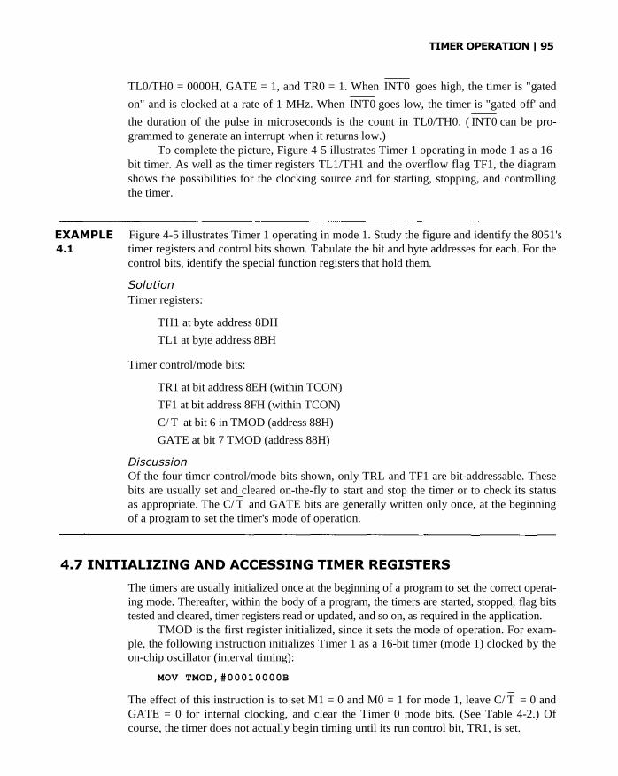
TIMER OPERATION | 95
TL0/TH0 = 0000H, GATE = 1, and TR0 = 1. When INT0 goes high, the timer is "gated
on" and is clocked at a rate of 1 MHz. When INT0 goes low, the timer is "gated off' and
the duration of the pulse in microseconds is the count in TL0/TH0. ( INT0 can be pro-grammed to generate an interrupt when it returns low.)
To complete the picture, Figure 4-5 illustrates Timer 1 operating in mode 1 as a 16-bit timer. As well as the timer registers TL1/TH1 and the overflow flag TF1, the diagramshows the possibilities for the clocking source and for starting, stopping, and controllingthe timer.
EXAMPLE Figure 4-5 illustrates Timer 1 operating in mode 1. Study the figure and identify the 8051's4.1 timer registers and control bits shown. Tabulate the bit and byte addresses for each. For the
control bits, identify the special function registers that hold them.
Solution
Timer registers:
TH1 at byte address 8DH
TL1 at byte address 8BH
Timer control/mode bits:
TR1 at bit address 8EH (within TCON)
TF1 at bit address 8FH (within TCON)
C/ T at bit 6 in TMOD (address 88H)
GATE at bit 7 TMOD (address 88H)
Discussion
Of the four timer control/mode bits shown, only TRL and TF1 are bit-addressable. Thesebits are usually set and cleared on-the-fly to start and stop the timer or to check its statusas appropriate. The C/ T and GATE bits are generally written only once, at the beginningof a program to set the timer's mode of operation.
4.7 INITIALIZING AND ACCESSING TIMER REGISTERS
The timers are usually initialized once at the beginning of a program to set the correct operat-ing mode. Thereafter, within the body of a program, the timers are started, stopped, flag bitstested and cleared, timer registers read or updated, and so on, as required in the application.
TMOD is the first register initialized, since it sets the mode of operation. For exam-ple, the following instruction initializes Timer 1 as a 16-bit timer (mode 1) clocked by theon-chip oscillator (interval timing):
MOV TMOD,#00010000B
The effect of this instruction is to set M1 = 0 and M0 = 1 for mode 1, leave C/ T = 0 andGATE = 0 for internal clocking, and clear the Timer 0 mode bits. (See Table 4-2.) Ofcourse, the timer does not actually begin timing until its run control bit, TR1, is set.

96 | CHAPTER 4
If an initial count is necessary, the timer registers TL1/TH1 must also be initialized.Remembering that the timers count up and set the overflow flag on an 0FFFFH-to-0000Htransition, a 100 µs interval could be timed by initializing TL1/TH1 to 100 counts less than0000H. The correct value is -100 or 0FF9CH. The following instructions do the job:
MOV TL1,#9CHMOV TH1,#0FFH
The timer is then started by setting the run control bit as follows:
SETB TR1
The overflow flag is automatically set 100 µs later. Software can sit in a "wait loop" for100 µs using a conditional branch instruction that returns to itself as long as the overflowflag is not set:
WAIT: JNB TF1,WAIT
When the timer overflows, it is necessary to stop the timer and clear the overflow flag in
software:
CLR TR1CLR TF1
4.7.1 Reading a Timer "on the Fly"
In some applications, it is necessary to read the value in the timer registers "on the fly."There is a potential problem that is simple to guard against in software. Since two timer reg-isters must be read, a "phase error" may occur if the low-byte overflows into the high-bytebetween the two read operations. A value may be read that never existed. The solution is toread the high-byte first, then the low-byte, and then read the high-byte again. If the high-byte has changed, repeat the read operations. The instructions below read the contents of thetimer registers TL1/TH1 into registers R6/R7, correctly dealing with this problem.
AGAIN: MOV A,THHMOV R6,TL1
CJNE A,THH,AGAINMOV R7,A
4.8 SHORT, MEDIUM, AND LONG INTERVALS
What is the range of intervals that can be timed? This issue is examined assuming the 8051is operating from a 12 MHz crystal. The on-chip oscillator is divided by 12 and clocks thetimers at a rate of 1 MHz.
The shortest possible interval is limited, not by the timer clock frequency, but bysoftware. Presumably, something must occur at regular intervals, and it is the duration ofinstructions that limit this for very short intervals. The shortest instruction on the 8051 isone machine cycle or one microsecond. Table 4-5 summarizes the techniques for creatingintervals of various lengths. (Operation from a 12 MHz crystal is assumed.)

TIMER OPERATION | 97
TABLE 4-5
Techniques for programming timed intervals (12 MHz operation)
EXAMPLE Pulse Wave Generation
4.2 Write a program that creates a periodic waveform on P1.0 with as high a frequency aspossible. What are the frequency and duty cycle of the waveform?
Solution
Discussion
This program creates a pulse waveform on P1.0 with a period of 4 µs. and a frequency of250 kHz. In each cycle, the signal is high for 1 µs. and low for 3 µs. This corresponds to aduty cycle of 1/4 = 0.25 or 25% (see Figure 4-6).
It might appear at first that the instructions in Figure 4-6 are misplaced, but they arenot. The SETB P1.0 instruction, for example, does not actually set the port bit until the endof the instruction, during S6P2.
The period of the waveform can be lengthened by inserting NOP instructions into theloop. Each NOP adds 1 machine cycle or 1 µs to the period of the waveform. For example,adding two NOP instructions after the SETB P1.0 instruction would make the output a squarewave (duty cycle = 50%) with a period of 6 µs and a frequency of 166.7 kHz. Beyond a point,software tuning is cumbersome, and a timer is the best choice to create time delays.
FIGURE 4-6
Waveform for example

98 | CHAPTER 4
EXAMPLE Square Wave Generation4.3 Write a program that creates a square wave on P1.0 with as high a frequency as possible.
What are the frequency and duty cycle of the waveform?
Solution
Discussion
The period is 6 µs : high-time = low-time = 3 µs. The frequency is 166.67 kHz and the dutycycle is 50% so this is a square wave, in contrast to the previous example which was not asquare wave.
Moderate-length intervals are easily obtained using 8-bit auto-reload mode, mode 2.Since the timed interval is set by an 8-bit count, the longest possible interval before overflowis 28 = 256 µs.
EXAMPLE 10 kHz Square Wave4.4 Write a program using Timer 0 to create a 10 kHz square wave on P1.0.
Solution
DiscussionThe program above creates a square wave on P1.0 with a high-time of 50 µs and a low-time of50 µs. Since the interval is less than 256 µs, timer mode 2 can be used. An overflow every 50µs requires a TH0 reload value of 50 counts less than 00H, or -50.
The program uses a complement bit instruction (CPL, line 12) rather than SETB andCLR. Between each complement operation, a delay of 1/2 the desired period (50 µs) isprogrammed using Timer 0 in 8-bit auto-reload mode. The reload value is specified usingdecimal notation as -50 (line 8), rather than using hexadecimal notation. The assemblerperforms the necessary conversion. Note that the timer overflow flag (TF0) is explicitlycleared in software after each overflow (line 11).
Timed intervals longer than 256 µs must use 16-bit timer mode, mode 1. The longestdelay is 216 = 65,536 µs or about 0.066 seconds. The inconvenience of mode 1 is that the

TIMER OPERATION | 99
timer registers must be reinitialized after each overflow, whereas reloading is automatic in
mode 2.
EXAMPLE 1 kHz Square Wave4.5 Write a program using Timer 0 to create a 1kHz square wave on P1.0.
Solution
DiscussionA 1 kHz square wave requires a high-time of 500 µs and a low-time of 500 µs. Since theinterval is longer than 256 µs, mode 2 cannot be used. Full 16-bit timer mode, mode 1, isrequired. The main difference in the software is that the timer registers, TL0 and TH0, arereinitialized after each overflow (lines 8 and 9).
There is a slight discrepancy in the output frequency in the program above. Thisresults from the extra instructions inserted after the timer overflow to reinitialize the timer.If exactly 1 kHz is required, the reload value for TL0/TH0 must be adjusted somewhat.Such errors do not occur in auto-reload mode, since the timer is never stoppe - it overflowsat a consistent rate set by the reload value in TH0.
Since there are two timers in the 8051, a program could make use of them to simul-taneously generate two different waveforms on separate port pins.
EXAMPLE Using Two Timers Simultaneously4.6 Write a program that creates a square wave on P1.0 with a frequency of 10kHz and a square
wave on P2.0 with a frequency of 1kHz.
Solution

100 | CHAPTER 4
DiscussionBoth timers 0 and 1 are used in this case to simultaneously generate two square waves onP1.0 and P2.0, respectively. The value written into TMOD initializes both timers at thesame time. Even though the timers are running simultaneously, the testing for overflow hasto be done in sequence. Timer 0 is checked first since its period is smaller in order to avoidmissing its overflows. Notice that Timer 0 is set to operate in mode 2 auto-reload mode sothere is no need to reload the count after every overflow. Meanwhile, Timer 1 operates inmode 1 so its count must be reloaded every time an overflow occurs.
Intervals longer than 0.066 seconds can be achieved by cascading Timer 0 andTimer 1 through software, but this ties up both timers. A more practical approach uses oneof the timers in 16-bit mode with a software loop counting overflows. The desiredoperation is performed every n overflows.
EXAMPLE Buzzer Interface
4.7 A buzzer is connected to P1.7, and a debounced switch is connected to P1.6 (see Figure 4-7).Write a program that reads the logic level provided by the switch and sounds the buzzer for 1second for each 1-to-0 transition detected.
Solution
TIMER OPERATION | 101
DiscussionThe buzzer in Figure 4-7 is a piezo ceramic transducer that vibrates when stimulated with aDC voltage. A typical example is the Projects Unlimited AI-430 that generates a tone ofabout 3 kHz at 5 volts DC. An inverter is used as a driver since the AI-430 draws 7 mA ofcurrent. As indicated in the 8051's DC Characteristics in Appendix E, Port 1pins can sink amaximum of 1.6 mA. The AI-430 costs a few dollars.
The main loop in the software consists of six instructions (lines 10-15). In line 10, aone-instruction loop is executed to wait for the input signal on P1.7 to go high. Then an-other one-instruction loop (line 11) executes to wait for the input signal to go low. Whenthis happens, the buzzer sounds for 1 second. This is implemented in the next three in-structions. First, P1.7 is set to sound the buzzer (line 12); second, a 1-second delay sub-routine is called (line 13), and, third, P1.7 is cleared to silence the buzzer (line 14). Thenthe main loop is executed again (line 15).
The delay subroutine (lines 17-25) uses the technique identified in Table 4-6 as "16-bit timer plus software loops." In theory, delays of any length can be created. In thisexample, a 1-second delay is created by using a count of —10,000 for TH0/TL0 with 16-bit timer mode. The effect is to create a 10,000 µs delay. This delay (lines 18-23) isenclosed within a loop that executes 100 times, using R7 as a counter. The effect is a 1-second delay.
FIGURE 4-7 Buzzer example
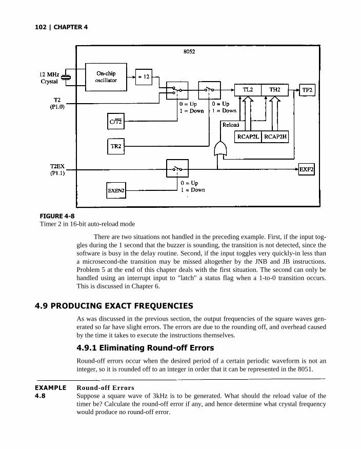
102 | CHAPTER 4
FIGURE 4-8
Timer 2 in 16-bit auto-reload mode
There are two situations not handled in the preceding example. First, if the input tog-gles during the 1 second that the buzzer is sounding, the transition is not detected, since thesoftware is busy in the delay routine. Second, if the input toggles very quickly-in less thana microsecond-the transition may be missed altogether by the JNB and JB instructions.Problem 5 at the end of this chapter deals with the first situation. The second can only behandled using an interrupt input to "latch" a status flag when a 1-to-0 transition occurs.This is discussed in Chapter 6.
4.9 PRODUCING EXACT FREQUENCIES
As was discussed in the previous section, the output frequencies of the square waves gen-erated so far have slight errors. The errors are due to the rounding off, and overhead causedby the time it takes to execute the instructions themselves.
4.9.1 Eliminating Round-off Errors
Round-off errors occur when the desired period of a certain periodic waveform is not aninteger, so it is rounded off to an integer in order that it can be represented in the 8051.
EXAMPLE Round-off Errors4.8 Suppose a square wave of 3kHz is to be generated. What should the reload value of the
timer be? Calculate the round-off error if any, and hence determine what crystal frequencywould produce no round-off error.

TIMER OPERATION | 103
Solution
A frequency of 3 kHz means the period should be 333.33 µs, so the high-time = low-time= 166.67 s. Since the 8051 can only handle integer count values, the timer reload valueshould be 167 counts before overflow, or —167. Notice that we have rounded off thedesired count to an integer value. The actual period is hence 167 x 2 x 1s = 334 µs so theactual frequency is 2.994 kHz. The round-off error is:
Discussion
Our previous examples used a crystal frequency of 12 MHz but that causes round-offerrors. Assuming that a count of 167 is used, our goal is to calculate the crystal frequencyso that an exact square wave with a frequency of 3 kHz is obtained.
Desired period = 333.33 µs so
4.9.2 Compensating for Overhead Due to Instructions
Instructions take some time to be carried out. The simplest of instructions require onemachine cycle while the most complex ones require 4. Therefore, instructions also add tothe time delay and if we prefer exact frequencies, we would need to adjust our initial timercounts to compensate for the overhead caused by the execution of these instructions.Example 4.9 considers a very simple demonstration of this.
EXAMPLE Rewrite the program of Example 4.5 to compensate for the overhead delay due to instructions4.9 in the program.
Solution
8H00 H ORG 8H00H8H00 75890H 2 MOV TMOD, #0HH ;H6-bit timer mode
8103 758CFE 3 LOOP: MOV TH0, #0FEH ;-490 (high byte)
104 | CHAPTER 4
Discussion
The program is exactly the same as that in Example 4.5. Only the reload value is different.In this case, a value of -490 was chosen to compensate for the overhead due to instruc-tions. Let's analyze to see why we chose this value.
TABLE 4-6
T2CON (Timer 2 control) register summary
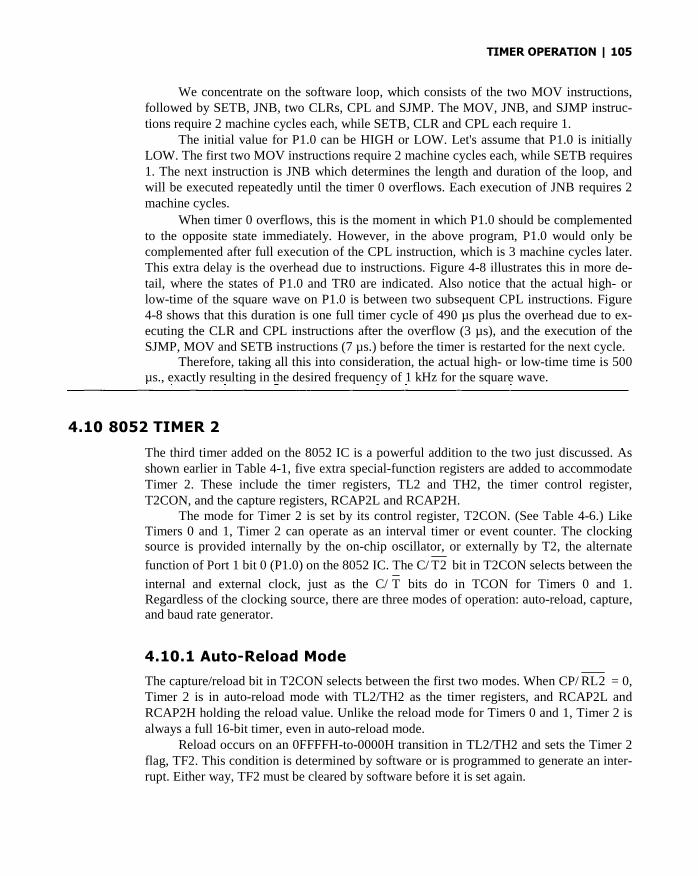
TIMER OPERATION | 105
We concentrate on the software loop, which consists of the two MOV instructions,followed by SETB, JNB, two CLRs, CPL and SJMP. The MOV, JNB, and SJMP instruc-tions require 2 machine cycles each, while SETB, CLR and CPL each require 1.
The initial value for P1.0 can be HIGH or LOW. Let's assume that P1.0 is initiallyLOW. The first two MOV instructions require 2 machine cycles each, while SETB requires1. The next instruction is JNB which determines the length and duration of the loop, andwill be executed repeatedly until the timer 0 overflows. Each execution of JNB requires 2machine cycles.
When timer 0 overflows, this is the moment in which P1.0 should be complementedto the opposite state immediately. However, in the above program, P1.0 would only becomplemented after full execution of the CPL instruction, which is 3 machine cycles later.This extra delay is the overhead due to instructions. Figure 4-8 illustrates this in more de-tail, where the states of P1.0 and TR0 are indicated. Also notice that the actual high- orlow-time of the square wave on P1.0 is between two subsequent CPL instructions. Figure4-8 shows that this duration is one full timer cycle of 490 µs plus the overhead due to ex-ecuting the CLR and CPL instructions after the overflow (3 µs), and the execution of theSJMP, MOV and SETB instructions (7 µs.) before the timer is restarted for the next cycle.
Therefore, taking all this into consideration, the actual high- or low-time time is 500µs., exactly resulting in the desired frequency of 1 kHz for the square wave.
4.10 8052 TIMER 2
The third timer added on the 8052 IC is a powerful addition to the two just discussed. Asshown earlier in Table 4-1, five extra special-function registers are added to accommodateTimer 2. These include the timer registers, TL2 and TH2, the timer control register,T2CON, and the capture registers, RCAP2L and RCAP2H.
The mode for Timer 2 is set by its control register, T2CON. (See Table 4-6.) LikeTimers 0 and 1, Timer 2 can operate as an interval timer or event counter. The clockingsource is provided internally by the on-chip oscillator, or externally by T2, the alternate
function of Port 1 bit 0 (P1.0) on the 8052 IC. The C/ T2 bit in T2CON selects between the
internal and external clock, just as the C/ T bits do in TCON for Timers 0 and 1.Regardless of the clocking source, there are three modes of operation: auto-reload, capture,and baud rate generator.
4.10.1 Auto-Reload Mode
The capture/reload bit in T2CON selects between the first two modes. When CP/ RL2 = 0,Timer 2 is in auto-reload mode with TL2/TH2 as the timer registers, and RCAP2L andRCAP2H holding the reload value. Unlike the reload mode for Timers 0 and 1, Timer 2 isalways a full 16-bit timer, even in auto-reload mode.
Reload occurs on an 0FFFFH-to-0000H transition in TL2/TH2 and sets the Timer 2flag, TF2. This condition is determined by software or is programmed to generate an inter-rupt. Either way, TF2 must be cleared by software before it is set again.
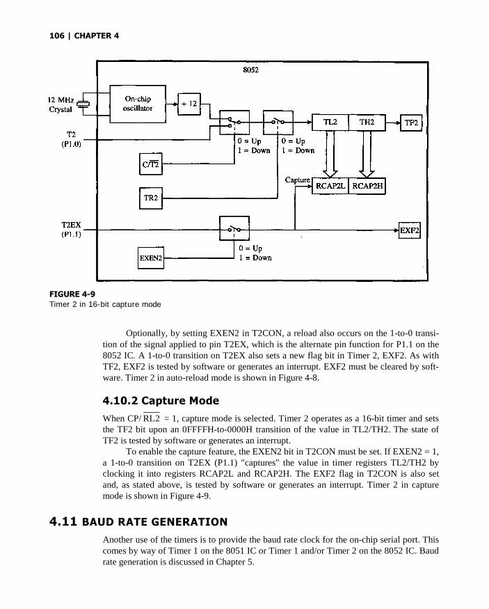
106 | CHAPTER 4
FIGURE 4-9
Timer 2 in 16-bit capture mode
Optionally, by setting EXEN2 in T2CON, a reload also occurs on the 1-to-0 transi-tion of the signal applied to pin T2EX, which is the alternate pin function for P1.1 on the8052 IC. A 1-to-0 transition on T2EX also sets a new flag bit in Timer 2, EXF2. As withTF2, EXF2 is tested by software or generates an interrupt. EXF2 must be cleared by soft-ware. Timer 2 in auto-reload mode is shown in Figure 4-8.
4.10.2 Capture Mode
When CP/ RL2 = 1, capture mode is selected. Timer 2 operates as a 16-bit timer and setsthe TF2 bit upon an 0FFFFH-to-0000H transition of the value in TL2/TH2. The state ofTF2 is tested by software or generates an interrupt.
To enable the capture feature, the EXEN2 bit in T2CON must be set. If EXEN2 = 1,a 1-to-0 transition on T2EX (P1.1) "captures" the value in timer registers TL2/TH2 byclocking it into registers RCAP2L and RCAP2H. The EXF2 flag in T2CON is also setand, as stated above, is tested by software or generates an interrupt. Timer 2 in capturemode is shown in Figure 4-9.
4.11 BAUD RATE GENERATION
Another use of the timers is to provide the baud rate clock for the on-chip serial port. Thiscomes by way of Timer 1 on the 8051 IC or Timer 1 and/or Timer 2 on the 8052 IC. Baudrate generation is discussed in Chapter 5.

TIMER OPERATION | 107
SUMMARY
This chapter has introduced the 8051 and 8052 timers. The software solutions for theexamples presented here feature one common but rather limiting trait. They consume allof the CPU's execution time. The programs execute in wait loops, waiting for a timeroverflow. This is fine for learning purposes, but for practical control-oriented applicationsusing microcontrollers, the CPU must perform other duties and respond to external events,such as an operator entering a parameter from a keyboard. In the chapter on interrupts, weshall demonstrate how to use the timers in an "interrupt-driven" environment. The timeroverflow flags are not tested in a software loop but generate an interrupt. Another programtemporarily interrupts the main program while an action is performed that affects the timerinterrupt (perhaps toggling a port bit). Through interrupts, the illusion of doing severalthings simultaneously is created.
PROBLEMS
4.1 Write an 8051 program that creates a square wave on P1.5 with a frequency of 100kHz. (Hint: Don't use the timers.)
4.2 What is the effect of the following instruction?
SETB 8EH
4.3 What is the effect of the following instruction?
MOV TMOD,#11010101B
4.4 Consider the three-instruction program shown in Example 4.2. What are the fre-quency and duty cycle of the waveform created on P1.0 for a 16 MHz 8051?
4.5 Rewrite the solution to Example 4.7 to include a "restart" mode. If a 1-to-0 transi-tion occurs while the buzzer is sounding, restart the timing loop to continue the buzzfor another second. This is illustrated in Figure 4-10.
4.6 Write an 8051 program to generate a 12 kHz square wave on P1.2 using Timer 0.4.7 Design a "turnstile" application using Timer 1 to determine when the 10,000th per-
son has entered a fairground. Assume (a) a turnstile sensor connects to TI and gen-erates a pulse each time the turnstile is rotated, and (b) a light is connected to P1.7that is on when P1.7 = 1, and off otherwise. Count "events" at T1 and turn on thelight at P1.7 when the 10,000th person enters the fairground. (See Figure 4-11.)
FIGURE 4-10Timing for modified
buzzer example
108 | CHAPTER
4
4
4
4
4
4
4
4
4
.8 The international tuning standard for musical instruments is "A above middle C" ata frequency of 440 Hz. Write an 8051 program to generate this tuning frequency andsound a 440 Hz tone on a loudspeaker connected to P1.1. (See Figure 4-12.) Due torounding of the values placed in TL1/TH1, there is a slight error in the output fre-quency. What is the exact output frequency, and what is the percentage error? Whatvalue of crystal would yield exactly 440 Hz with the program you have written?
.9 Write an 8051 program to generate a 500 Hz signal on P1.0, using Timer 0. Thewave form should have a 30% duty cycle (duty cycle = high-time / period).
.10 The circuit shown in Figure 4-13 will provide an extremely accurate 60 Hz signal toT2 by tapping the secondary of a power supply transformer. Initialize Timer 2 suchthat it is clocked by T2 and overflows once per second. Upon each overflow, updatea time-of-day value stored in the 8052's internal memory at locations 50H (hours),51H (minutes), and 52H (seconds). More timer examples and problems are found inChapter 6.
.11 a. Write the program to generate a (30% duty cycle) rectangular pulse wave onP1.0, and a square wave on P2.0.
b. Hence, determine the (i) round-off error, and (ii) error due to instructionoverhead for both waveforms.
.12 Write a program to generate a 2.5 kHz waveform on P1.0 with a 20% duty cycle.Show your workings and write comments for each line of the code.
.13 Consider an external crystal oscillator with a frequency of 16 MHz instead of the stan-dard 12MHz. Write a program to generate a periodic waveform on P1.0 with the highestpossible frequency. Hence, calculate the frequency and duty cycle of that waveform.
.14 Suppose you want to use the 8051's timer to time the duration of 1 hour. Whatmode should you ask the timer to be in? Why?4.15 Suppose you are required to generate a square waveform on P1.0 with afrequency of 21 kHz having a duty cycle of 10%, what mode should you use the timerin? Why?
.16 What is the highest value that an 8051 timer can count to? If you use an 8051's timeras an event counter, what effect will it have on your counting? Why?
FIGURE 4-11Turnstile problem
FIGURE 4-12Loudspeaker interface

TIMER OPERATION | 109
FIGURE 4-13
60 Hz time base
4.17 What do you mean by a 16-bit timer? Explain.4.18 a. Write a program to generate a 3 kHz waveform on P2.0 with a 30% duty cycle.
Show your workings and write comments for each line of the code. Makeadjustments to overcome the delay overhead due to instructions.
b. For the program above, is there any truncation error? If so, calculate thepercentage error. If not, why do you say so?

110 | CHAPTER 4
Serial Port Operation
5.1 INTRODUCTION
The 8051 includes an on-chip serial port that can operate in several modes over a widerange of frequencies. The essential function of the serial port is to perform parallel-to-serial conversion for output data, and serial-to-parallel conversion for input data.
Hardware access to the serial port is through the TXD and RXD pins introduced inChapter 2. These pins are the alternate functions for two Port 3 bits, P3.1 on pin 11(TXD), and P3.0 on pin 10 (RXD).
The serial port features full duplex operation (simultaneous transmission and recep-tion) and receive buffering, allowing one character to be received and held in a bufferwhile a second character is received. If the CPU reads the first character before the secondis fully received, data are not lost.
The serial port frequency of operation, or baud rate, can be fixed (derived from the8051 on-chip oscillator) or variable. If a variable baud rate is used, Timer 1 supplies thebaud rate clock and must be programmed accordingly. (On the 8032/8052, Timer 2 can beprogrammed to supply the baud rate clock.)
Two special function registers, the serial port buffer register (SBUF) and the serialport control register (SCON), provide software access to the serial port.
5.2 SERIAL COMMUNICATION
Before we move on to discuss the operation of the 8051 serial port, we first touch on somebasic concepts of serial communication. Serial communication involves the transmission ofbits of data through only one communication line. The data are transmitted bit by bit in eithersynchronous or asynchronous format. Synchronous serial communication transmits onewhole block of characters in synchronization with a reference clock while asynchronous
111
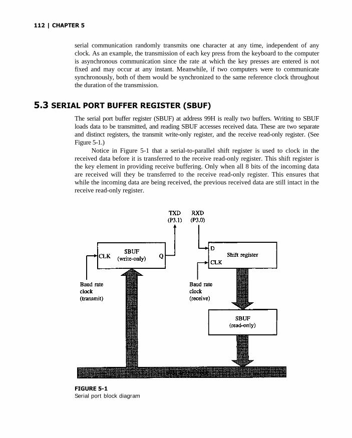
112 | CHAPTER 5
serial communication randomly transmits one character at any time, independent of anyclock. As an example, the transmission of each key press from the keyboard to the computeris asynchronous communication since the rate at which the key presses are entered is notfixed and may occur at any instant. Meanwhile, if two computers were to communicatesynchronously, both of them would be synchronized to the same reference clock throughoutthe duration of the transmission.
5.3 SERIAL PORT BUFFER REGISTER (SBUF)
The serial port buffer register (SBUF) at address 99H is really two buffers. Writing to SBUFloads data to be transmitted, and reading SBUF accesses received data. These are two separateand distinct registers, the transmit write-only register, and the receive read-only register. (SeeFigure 5-1.)
Notice in Figure 5-1 that a serial-to-parallel shift register is used to clock in thereceived data before it is transferred to the receive read-only register. This shift register isthe key element in providing receive buffering. Only when all 8 bits of the incoming dataare received will they be transferred to the receive read-only register. This ensures thatwhile the incoming data are being received, the previous received data are still intact in thereceive read-only register.
FIGURE 5-1
Serial port block diagram
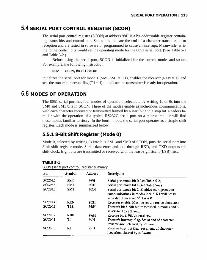
SERIAL PORT OPERATION | 113
5.4 SERIAL PORT CONTROL REGISTER (SCON)
The serial port control register (SCON) at address 98H is a bit-addressable register contain-ing status bits and control bits. Status bits indicate the end of a character transmission orreception and are tested in software or programmed to cause an interrupt. Meanwhile, writ-ing to the control bits would set the operating mode for the 8051 serial port. (See Table 5-1and Table 5-2.)
Before using the serial port, SCON is initialized for the correct mode, and so on.For example, the following instruction
MOV SCON,#01010010B
initializes the serial port for mode 1 (SM0/SM1 = 0/1), enables the receiver (REN = 1), andsets the transmit interrupt flag (T1 = 1) to indicate the transmitter is ready for operation.
5.5 MODES OF OPERATION
The 8051 serial port has four modes of operation, selectable by writing 1s or 0s into theSM0 and SM1 bits in SCON. Three of the modes enable asynchronous communications,with each character received or transmitted framed by a start bit and a stop bit. Readers fa-miliar with the operation of a typical RS232C serial port on a microcomputer will findthese modes familiar territory. In the fourth mode, the serial port operates as a simple shiftregister. Each mode is summarized below.
5.5.1 8-Bit Shift Register (Mode 0)
Mode 0, selected by writing 0s into bits SM1 and SM0 of SCON, puts the serial port into8-bit shift register mode. Serial data enter and exit through RXD, and TXD outputs theshift clock. Eight bits are transmitted or received with the least-significant (LSB) first.
TABLE 5-1SCON (serial port control) register summary

114 | CHAPTER 5
TABLE 5-2Serial Dort modes
The baud rate is fixed at 1/12th the on-chip oscillator frequency. The terms "RXD"and "TXD" are misleading in this mode. The RXD line is used for both data input and out-put, and the TXD line serves as the clock.
Transmission is initiated by any instruction that writes data to SBUF. Data are shifted outon the RXD line (P3.0) with clock pulses sent out the TXD line (P3.1). Each transmitted bit isvalid on the RXD pin for one machine cycle. During each machine cycle, the clock signal goeslow on S3P1 and returns high on S6P1. The timing for output data is shown in Figure 5-2.
Reception is initiated when the receiver enable bit (REN) is 1 and the receive interruptbit (RI) is 0. The general rule is to set REN at the beginning of a program to initialize theserial port and then clear RI to begin a data input operation. When RI is cleared, clockpulses are written out the TXD line, beginning the following machine cycle, and data areclocked in the RXD line. Obviously, it is up to the attached circuitry to provide data on the
FIGURE 5-2Serial port transmit timing for mode 0
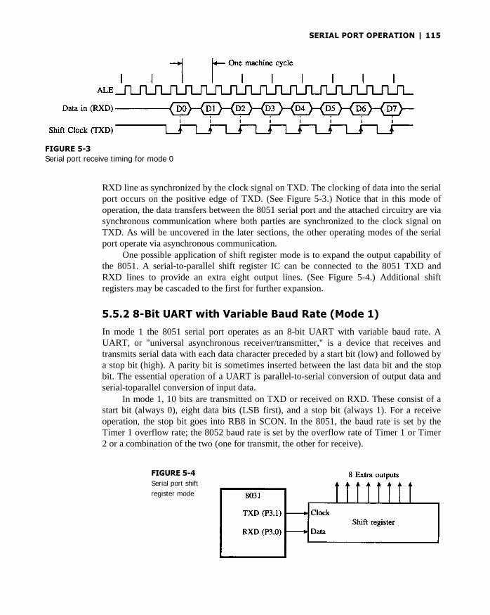
SERIAL PORT OPERATION | 115
FIGURE 5-3
Serial port receive timing for mode 0
RXD line as synchronized by the clock signal on TXD. The clocking of data into the serialport occurs on the positive edge of TXD. (See Figure 5-3.) Notice that in this mode ofoperation, the data transfers between the 8051 serial port and the attached circuitry are viasynchronous communication where both parties are synchronized to the clock signal onTXD. As will be uncovered in the later sections, the other operating modes of the serialport operate via asynchronous communication.
One possible application of shift register mode is to expand the output capability ofthe 8051. A serial-to-parallel shift register IC can be connected to the 8051 TXD andRXD lines to provide an extra eight output lines. (See Figure 5-4.) Additional shiftregisters may be cascaded to the first for further expansion.
5.5.2 8-Bit UART with Variable Baud Rate (Mode 1)
In mode 1 the 8051 serial port operates as an 8-bit UART with variable baud rate. AUART, or "universal asynchronous receiver/transmitter," is a device that receives andtransmits serial data with each data character preceded by a start bit (low) and followed bya stop bit (high). A parity bit is sometimes inserted between the last data bit and the stopbit. The essential operation of a UART is parallel-to-serial conversion of output data andserial-toparallel conversion of input data.
In mode 1, 10 bits are transmitted on TXD or received on RXD. These consist of astart bit (always 0), eight data bits (LSB first), and a stop bit (always 1). For a receiveoperation, the stop bit goes into RB8 in SCON. In the 8051, the baud rate is set by theTimer 1 overflow rate; the 8052 baud rate is set by the overflow rate of Timer 1 or Timer2 or a combination of the two (one for transmit, the other for receive).
FIGURE 5-4
Serial port shift
register mode

116| CHAPTER 5
FIGURE 5-6
Setting the seri
Clocking and synchronizing the serial port shift registers in modes 1, 2, and 3 isestablished by a 4-bit divide-by-16 counter, the output of which is the baud rate clock. (SeeFigure 5-5.) The input to this counter is selected through software, as discussed later.
Transmission is initiated by writing to SBUF but does not actually start until the nextrollover of the divide-by-16 counter supplying the serial port baud rate. Shifted data are out-putted on the TXD line beginning with the start bit, followed by the eight data bits, then the stopbit. The period for each bit is the reciprocal of the baud rate as programmed in the timer. Thetransmit interrupt flag (TI) is set as soon as the stop bit appears on TXD. (See Figure 5-6.)
Reception is initiated by a 1-to-0 transition on RXD. The divide-by-16 counter isimmediately reset to align the counts with the incoming bit stream (the next bit arrives onthe next divide-by-16 rollover, and so on). The incoming bit stream is sampled in themiddle of the 16 counts.
The receiver includes "false start bit detection" by requiring a 0 state eight countsafter the first 1-to-0 transition. If this does not occur, it is assumed that the receiver wastriggered by noise rather than by a valid character. The receiver is reset and returns to theidle state, looking for the next 1-to-0 transition.
Assuming a valid start bit was detected, character reception continues. The start bitskipped and eight data bits are clocked into the serial port shift register. When all eight bitshave been clocked in, the following occur:
1. The ninth bit (the stop bit) is clocked into RB8 in SCON,2. SBUF is loaded with the eight data bits, and3. The receiver interrupt flag (RI) is set.
al port T1 flag
FIGURE 5-5
Serial port clocking

SERIAL PORT OPERATION | 117
These only occur, however, if the following conditions exist:
1. RI = 0, and2. SM2 = 1 and the received stop bit = 1, or SM2 = 0.
The requirement that RI = 0 ensures that software has read the previous character(and cleared RI). The second condition sounds complicated but applies only in multi-processor communications mode (see below). It implies, "Do not set RI in multiprocessorcommunications mode when the ninth data bit is 0."
5.5.3 9-Bit UART with Fixed Baud Rate (Mode 2)
When SM1 = 1 and SM0 = 0, the serial port operates in mode 2 as a 9-bit UART with afixed baud rate. Eleven bits are transmitted or received: a start bit, eight data bits, a pro-grammable ninth data bit, and a stop bit. On transmission, the ninth bit is whatever hasbeen put in TB8 in SCON (perhaps a parity bit). On reception, the ninth bit received isplaced in RB8. The baud rate in mode 2 is either 1/32nd or 1/64th the on-chip oscillatorfrequency. (See 5.9 Serial Port Baud Rates.)
5.5.4 9-Bit UART with Variable Baud Rate (Mode 3)
Mode 3, 9-bit UART with variable baud rate, is the same as mode 2 except the baud rateis programmable and provided by the timer. In fact, modes 1, 2, and 3 are very similar.The differences lie in the baud rates (fixed in mode 2, variable in modes 1 and 3) and inthe number of data bits (eight in mode 1, nine in modes 2 and 3).
5.6 FULL DUPLEX SERIAL COMMUNICATION: ISSUES
The 8051's serial port allows for full duplex operation, which means that both transmission andreception of characters can be done simultaneously. However, there are some issues involved.
The first issue involves the physical connections. Full duplex communication mustuse two separate lines, one for transmission and one for reception, otherwise the signalsfrom both parties would collide. In mode 0 of the serial port operation, only one line, theRXD, is used for both transmission and reception, hence full duplex cannot be achieved inthis mode. In fact, as has been previously discussed in the section on the serial port modesof operation, mode 0 provides only half duplex operation. Meanwhile, all the other threemodes use two separate lines, TXD and RXD for transmission and reception respectively,hence they allow for full duplex operation.
Secondly, the timing and synchronization must be considered. A common questionasked by the student when told that the serial port can operate in full duplex is: "Suppose theserial port is transmitting a character to a serial device, so both the 8051 and the serial deviceare in synchronization. What would happen when in the midst of this, an incomingcharacter is detected on the RXD line?" This poses an interesting question. For an answerto this, there is a need to understand the internal structure of the serial port. The 8051 serialport consists of two physically separate SBUF registers as shown in Figure 5-1. The transmit

118 | CHAPTER 5
write-only register is clocked by a transmit baud rate clock while the receive read-only re-gister is clocked by a receive baud rate clock. Both clocks are based on the overflow rate ofTimer 1, as has been previously discussed (See Section 5.5.2 Mode 1.) Despite this fact,however, both baud rate clocks are separate and independent.
Transmission is initiated by writing to SBUF but only starts when the next rolloverof the transmit baud rate clock is detected. Meanwhile, if any incoming character is de-tected, the 1-to-0 transition that denotes the start bit will immediately reset the receive baudrate clock so that the 8051 is synchronized with the device attached to the serial port.
Towards the end of this chapter, an example that demonstrates the full duplex opera-tion of the serial port will be given.
5.7 INITIALIZATION AND ACCESSING SERIAL PORT REGISTERS
5.7.1 Receiver Enable
The receiver enable bit (REN) in SCON must be set by software to enable the reception ofcharacters. This is usually done at the beginning of a program when the serial port, timers,etc., are initialized. This can be done in two ways. The instruction
SETB REN
explicitly sets REN, or the instruction
MOV SCON,#xxx1xxxxB
sets REN and sets or clears the other bits in SCON, as required. (The x's must be 1s or 0sto set the mode of operation.)
5.7.2 The Ninth Data Bit
The ninth data bit transmitted in modes 2 and 3 must be loaded into TB8 by software. The ninthdata bit received is placed in RB8. Software may or may not require a ninth data bit, dependingon the specifications of the serial device with which communications are established. (The ninthdata bit also plays an important role in multiprocessor communications. See below.)
5.7.3 Adding a Parity Bit
A common use for the ninth data bit is to add parity to a character. As discussed in Chapter2, the P bit in the program status word (PSW) is set or cleared every machine cycle to es-tablish even parity with the eight bits in the accumulator. If, for example, communicationsrequire eight data bits plus even parity, the following instructions could be used to transmitthe eight bits in the accumulator with even parity added in the ninth bit:
MOV C,P ; PUT EVEN PARITY BIT IN TBSMOV TBS,C ; THIS BECOMES THE 9TH DATA BITMOV SBUF,A ; MOVE S BITS FROM ACC TO SBUF

SERIAL PORT OPERATION | 119
If odd parity is required, then the instructions must be modified as follows:
MOV C,P ; PUT EVEN PARITY BIT IN C FLAGCPL C ; CONVERT TO ODD PARITY
MOV TB8,CMOV SBUF,A
Of course, the use of parity is not limited to modes 2 and 3. In mode 1, the eightdata bits transmitted can consist of seven data bits plus a parity bit. In order to transmit a7-bit ASCII code with even parity in bit 8, the following instructions could be used:
CLR ACC.7 ; ENSURE MSB IS CLEAR
; EVEN PARITY IS IN P
MOV C,P ; COPY TO C
MOV ACC.7,C ; PUT EVEN PARITY INTO MSB
MOV SBUF,A ; SEND CHARACTER
; 7 DATA BITS PLUS EVEN PARITY
5.7.4 Interrupt Flags
The receive and transmit interrupt flags (RI and TI) in SCON play an important role in 8051serial communications. Both bits are set by hardware but must be cleared by software.
Typically, RI is set at the end of character reception and indicates "receive bufferfull." This condition is tested in software or programmed to cause an interrupt. (Interruptsare discussed in Chapter 6.) If software wishes to input a character from the device con-nected to the serial port (perhaps a video display terminal), it must wait until RI is set,then clear RI and read the character from SBUF. This is shown below.
WAIT: JNB RI,WAIT ; CHECK RI UNTIL SETCLR RI ; CLEAR RIMOV A,SBUF ; READ CHARACTER
TI is set at the end of character transmission and indicates "transmit buffer empty."If software wishes to send a character to the device connected to the serial port, it mustfirst check that the serial port is ready. In other words, if a previous character was sent,wait until transmission is finished before sending the next character. The followinginstructions transmit the character in the accumulator:
WAIT: JNB TI,WAIT ;CHECK TI UNTIL SET
CLR TI ;CLEAR TIMOV SBUF,A ;SEND CHARACTER
The receive and transmit instruction sequences above are usually part of standard inputcharacter and output character subroutines. These are described in more detail in Example5.2 and Example 5.3.
5.8 MULTIPROCESSOR COMMUNICATIONS
Modes 2 and 3 have a special provision for multiprocessor communications. In these modes,nine data bits are received and the ninth bit goes into RB8. The port can be programmed so

120 | CHAPTER 5
FIGURE 5-7Multiprocessor communication
that when the stop bit is received, the serial port interrupt is activated only if RB8 = 1. Thisfeature is enabled by setting the SM2 bit in SCON. An application of this is in a networkingenvironment using multiple 8051s in a master/slave arrangement, as shown in Figure 5-7.
When the master processor wants to transmit a block of data to one of several slaves,it first sends out an address byte that identifies the target slave. An address byte differsfrom a data byte in that the ninth bit is 1 in an address byte and 0 in a data byte. An addressbyte, however, interrupts all slaves, so that each can examine the received byte to test if itis being addressed. The addressed slave will clear its SM2 bit and prepare to receive thedata bytes that follow. The slaves that weren't addressed leave their SM2 bits set and goabout their business, ignoring the incoming data bytes. They will be interrupted again whenthe next address byte is transmitted by the master processor. Special schemes can bedevised so that once a master/slave link is established, the slave can also transmit to themaster. The trick is not to use the ninth data bit after a link has been established (otherwiseother slaves may be inadvertently selected).
SM2 has no effect in mode 0, and in mode 1 it can be used to check the validity ofthe stop bit. In mode 1 reception, if SM2 = 1, the receive interrupt will not be activated un-less a valid stop bit is received.
5.9 SERIAL PORT BAUD RATES
As evident in Table 5-2, the baud rate is fixed in modes 0 and 3. In mode 0 it is always theon-chip oscillator frequency divided by 12. Usually a crystal drives the 8051's on-chiposcillator, but another clock source can be used as well. (See Chapter 2.) Assuming anominal oscillator frequency of 12 MHz, the mode 0 baud rate is 1 MHz. (See Figure 5-8a.)
By default following a system reset, the mode 2 baud rate is the oscillator frequencydivided by 64. The baud rate is also affected by a bit in the power control register, PCON.

SERIAL PORT OPERATION | 121
FIGURE 5-8Serial port clocking sources (a) Mode 0 (b) Mode 2 (c) Modes 1 and 3
Bit 7 of PCON is the SMOD bit. Setting SMOD has the effect of doubling the baud rate inmodes 1, 2, and 3. In mode 2, the baud rate can be doubled from a default value of 1/64ththe oscillator frequency (SMOD = 0), to 1/32nd the oscillator frequency (SMOD = 1). (SeeFigure 5-8b.)
Since PCON is not bit-addressable, setting SMOD without altering the other PCONbits requires a "read-modify-write" operation. The following instructions set SMOD:
MOV A,PCON ;GET CURRENT VALUE OF PCONSETB ACC.7 ;SET BIT 7 (SMOD)MOV PCON,A ;WRITE VALUE BACK TO PCON
The 8051 baud rates in modes 1 and 3 are determined by the Timer 1 overflow rate. Sincethe timer operates at a relatively high frequency, the overflow is further divided by 32 (16if SMOD = 1) before providing the baud rate clock to the serial port. The 8052 baud ratein modes 1 and 3 is determined by the Timer 1 or Timer 2 overflow rates, or both.
5.9.1 Using Timer 1 as the Baud Rate Clock
Considering only an 8051 for the moment, the usual technique for baud rate generation is toinitialize TMOD for 8-bit auto-reload mode (timer mode 2) and put the correct reload valuein TH1 to yield the proper overflow rate for the baud rate. TMOD is initialized as follows:
MOV TMOD,#0010xxxxB
The x's are 1s or 0s as needed for Timer 0.

122 | CHAPTER 5
This is not the only possibility. Very low baud rates can be achieved by using 16-bitmode, timer mode 2 with TMOD = 0001xxxxB. There is a slight software overhead,however, since the TH1/TL1 registers must be reinitialized after each overflow. Thiswould be performed in an interrupt service routine. Another option is to clock Timer 1externally using T1 (P3.5). Regardless the baud rate is the Timer 1 overflow rate dividedby 32 (or divided by 16, if SMOD = 1).
The formula for determining the baud rate in modes 1 and 3, therefore, is
BAUD RATE = TIMER1 OVERFLOW RATE 32
For example, 1200 baud operation requires an overflow rate calculated as follows:
1200 = TIMER1 OVERFLOW RATE 32TIMER1 OVERFLOW RATE = 38.4 kHz
If a 12 MHz crystal drives the on-chip oscillator, Timer 1 is clocked at a rate of 1MHz or 1000 kHz. Since the timer must overflow at a rate of 38.4 kHz and the timer isclocked at a rate of 1000 kHz, an overflow is required every 1000 38.4 = 26.04 clocks.(Round to 26.) Since the timer counts up and overflows on the 0FFH-to-00H transition ofthe count, 26 counts less than 0 is the required reload value for TH1. The correct value is-26. The easiest way to put the reload value into TH1 is
MOV TH1,#-26
The assembler will perform the necessary conversion. In this case -26 is convertedto 0E6H; thus, the instruction above is identical to
MOV TH1,#0E6H
Due to rounding, there is a slight error in the resulting baud rate. Generally, a 5% er-ror is tolerable using asynchronous (start/stop) communications. Exact baud rates are pos-sible using an 11.059 MHz crystal. Table 5-3 summarizes the TH1 reload values for themost common baud rates, using a 12.000 MHz or 11.059 MHz crystal.
TABLE 5-3Baud rate summary
TH1 Reload Actual Baud
Baud Rate Crystal Frequency SMOD Value Rate Error
9600 12.000 MHz 1 -7 (0F9H) 8923 7%2400 12.000 MHz 0 -13 (0F3H) 2404 0.16%1200 12.000 MHz 0 -26 (0E6H) 1202 0.16%19200 11.059 MHz 1 -3 (0FDH) 19200 09600 11.059 MHz 0 -3 (0FDH) 9600 02400 11.059 MHz 0 -12 (0F4H) 2400 01200 11.059 MHz 0 -24 (0E8H) 1200 0
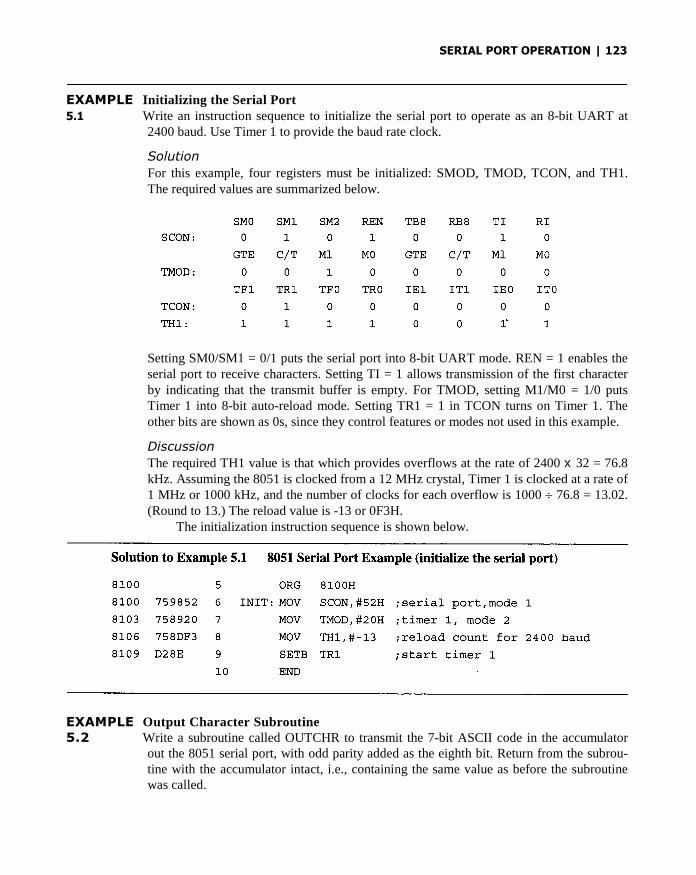
SERIAL PORT OPERATION | 123
EXAMPLE Initializing the Serial Port5.1 Write an instruction sequence to initialize the serial port to operate as an 8-bit UART at
2400 baud. Use Timer 1 to provide the baud rate clock.
Solution
For this example, four registers must be initialized: SMOD, TMOD, TCON, and TH1.The required values are summarized below.
Setting SM0/SM1 = 0/1 puts the serial port into 8-bit UART mode. REN = 1 enables theserial port to receive characters. Setting TI = 1 allows transmission of the first characterby indicating that the transmit buffer is empty. For TMOD, setting M1/M0 = 1/0 putsTimer 1 into 8-bit auto-reload mode. Setting TR1 = 1 in TCON turns on Timer 1. Theother bits are shown as 0s, since they control features or modes not used in this example.
Discussion
The required TH1 value is that which provides overflows at the rate of 2400 x 32 = 76.8kHz. Assuming the 8051 is clocked from a 12 MHz crystal, Timer 1 is clocked at a rate of1 MHz or 1000 kHz, and the number of clocks for each overflow is 1000 76.8 = 13.02.(Round to 13.) The reload value is -13 or 0F3H.
The initialization instruction sequence is shown below.
EXAMPLE Output Character Subroutine5.2 Write a subroutine called OUTCHR to transmit the 7-bit ASCII code in the accumulator
out the 8051 serial port, with odd parity added as the eighth bit. Return from the subrou-tine with the accumulator intact, i.e., containing the same value as before the subroutinewas called.

124 | CHAPTER 5
Solution
This example and the next illustrate two of the most common subroutines on microcom-puter systems with an attached RS232 terminal: output character (OUTCHR) and inputcharacter (INCHAR).
8100 5 ORG 8100H
8100 A2D0 6 OUTCHR: MOV C.P ;put parity bit in C flag
8102 B3 7 CPL C ;change to odd parity
8103 92E7 8 MOV ACC.7.C ;add to character code
8105 3099FD 9 AGAIN: JNB TI.AGAIN ;Tx empty? no:check again
8108 C299 10 CLR TI ;yes: clear flag and
810A F599 11 MOV SBUF.A ;send character
810C C2E7 12 CLR ACC.7 ;strip off parity bit and
810E 22 13 RET ; return
14 END
Discussion
The first three instructions place odd parity in the accumulator bit 7. Since the P bit in thePSW establishes even parity with the accumulator, it is complemented before being placedin ACC.7. The JNB instruction creates a "wait loop," repeatedly testing the transmit inter-rupt flag (TI) until it is set. When TI is set (because the previous character transmission isfinished), it is cleared and then the character in the accumulator is written into the serialport buffer (SBUF). Transmission begins on the next rollover of the divide-by-l6 counterthat clocks the serial port. (See Figure 5-5.) Finally, ACC.7 is cleared so that the returnvalue is the same as the 7-bit code passed to the subroutine.
The OUTCHR subroutine is a building block and is of little use by itself. At a"higher level" this subroutine is called to transmit a single character or a string ofcharacters. For example, the following instructions transmit the ASCII code for the letter"Z" to the serial device attached to the 8051's serial port:
MOV A.#'Z'
CALL OUTCHR
(continue)
As a natural extension to this idea, Problem 1 at the end of this chapter uses OUTCHR asa building block in an OUTSTR (output string) subroutine that transmits a sequence ofASCII codes (terminated by a NULL byte, 00H) to the serial device attached to the 8051'sserial port.
EXAMPLE Input Character Subroutine5.3 Write a subroutine called INCHAR to input a character from the 8051's serial port and re-
turn with the 7-bit ASCII code in the accumulator. Expect odd parity in the eighth bit re-ceived and set the carry flag if there is a parity error.

SERIAL PORT OPERATION | 125
Solution
Discussion
This subroutine begins by waiting for the receive interrupt flag (RI) to be set, indicatingthat a character is waiting in SBUF to be read. When RI is set, the JNB instruction fallsthrough to the next instruction. RI is cleared and the code in SBUF is read into the accu-mulator. The P bit in the PSW establishes even parity with the accumulator, so it shouldbe set if the accumulator, on its own, correctly contains odd parity in bit 7. Moving the Pbit into the carry flag and complementing it leaves CY = 0 if there is no error. On theother hand, if the accumulator contains a parity error, then CY = 1, correctly indicating"parity error." Finally, ACC.7 is cleared to ensure that only a 7-bit code is returned to thecalling program.
EXAMPLE Full Duplex Operation5.4 Write a program that continually transmits characters from a transmit buffer (internal
RAM 30H to 4FH). If incoming characters are detected on the serial port, store them inthe receive buffer starting at internal RAM location 50H. Assume that the 8051 serial porthas already been initialized in mode H.
Solution
This example shows how the serial port can be used in full duplex operation, i.e., trans-mission and reception are done simultaneously.

126 | CHAPTER 5
Discussion
This program first uses the two registers R0 and R1 to point to the transmit and receivebuffers respectively. It then checks to see if a character has been received or if theprevious character to be transmitted has already been sent out. Notice that reception isprocessed first. This is because reception is more critical since the 8051 is depending onan external device for an incoming character, which must be processed and stored as soonas possible else it might be overwritten by subsequent incoming characters. Recall that theserial port can hold at most one character in its buffer while a second is being received. Ifan incoming character has been fully received, it is read from SBUF and checked forparity before being stored into the receive buffer whose current empty location is pointedto by R1. R1 is next incremented to point to the next available location and the programgoes back to checking. When the previous transmission is finished, the program first getsthe character to be transmitted from the transmit buffer. R0 is used as the pointer to thenext character in the transmit buffer. The odd parity is then placed in bit 7 of the codebefore it is sent to the SBUF for transmission. R1 is then incremented to point to the nextcharacter. The program also checks for the end of the transmit buffer, upon which itwould recycle back to the beginning of the buffer. Finally, the program goes back tochecking for further receptions or transmission.
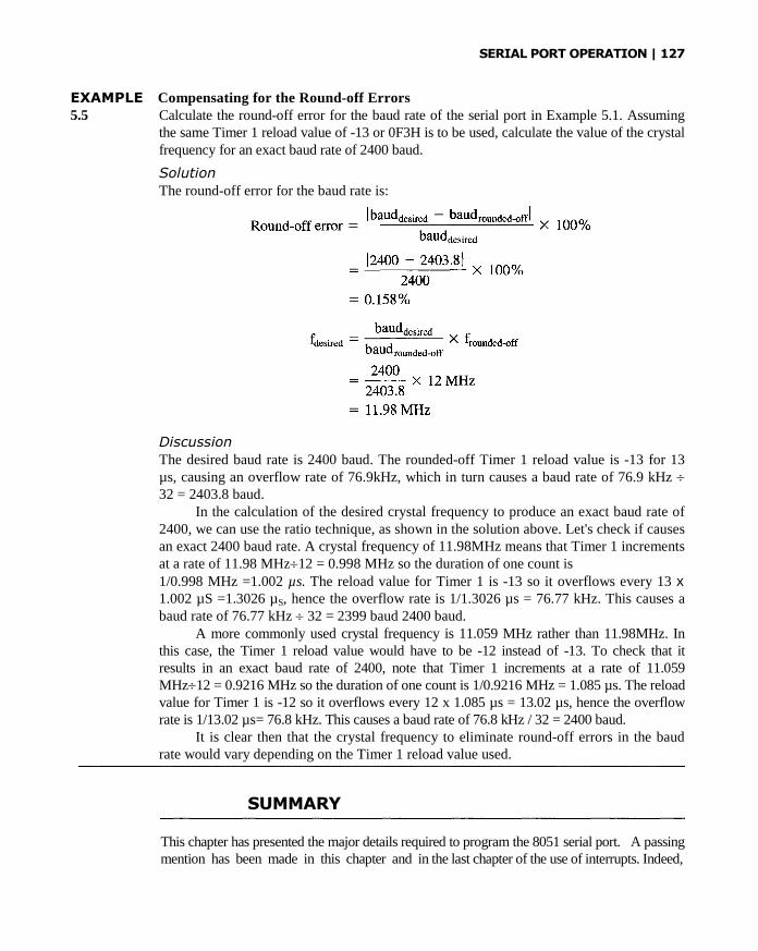
SERIAL PORT OPERATION | 127
EXAMPLE Compensating for the Round-off Errors5.5 Calculate the round-off error for the baud rate of the serial port in Example 5.1. Assuming
the same Timer 1 reload value of -13 or 0F3H is to be used, calculate the value of the crystalfrequency for an exact baud rate of 2400 baud.
Solution
The round-off error for the baud rate is:
Discussion
The desired baud rate is 2400 baud. The rounded-off Timer 1 reload value is -13 for 13µs, causing an overflow rate of 76.9kHz, which in turn causes a baud rate of 76.9 kHz 32 = 2403.8 baud.
In the calculation of the desired crystal frequency to produce an exact baud rate of2400, we can use the ratio technique, as shown in the solution above. Let's check if causesan exact 2400 baud rate. A crystal frequency of 11.98MHz means that Timer 1 incrementsat a rate of 11.98 MHz12 = 0.998 MHz so the duration of one count is1/0.998 MHz =1.002 µs. The reload value for Timer 1 is -13 so it overflows every 13 x1.002 µS =1.3026 µS, hence the overflow rate is 1/1.3026 µs = 76.77 kHz. This causes abaud rate of 76.77 kHz 32 = 2399 baud 2400 baud.
A more commonly used crystal frequency is 11.059 MHz rather than 11.98MHz. Inthis case, the Timer 1 reload value would have to be -12 instead of -13. To check that itresults in an exact baud rate of 2400, note that Timer 1 increments at a rate of 11.059MHz12 = 0.9216 MHz so the duration of one count is 1/0.9216 MHz = 1.085 µs. The reloadvalue for Timer 1 is -12 so it overflows every 12 x 1.085 µs = 13.02 µs, hence the overflowrate is 1/13.02 µs= 76.8 kHz. This causes a baud rate of 76.8 kHz / 32 = 2400 baud.
It is clear then that the crystal frequency to eliminate round-off errors in the baudrate would vary depending on the Timer 1 reload value used.
SUMMARY
This chapter has presented the major details required to program the 8051 serial port. A passingmention has been made in this chapter and in the last chapter of the use of interrupts. Indeed,
128 | CHAPTER 5
advanced applications using the 8051 timers or serial ports generally require input/outputoperations to be synchronized by interrupts. This is the topic of the next chapter.
PROBLEMS
The following problems are typical of the software routines for interfacing terminals (orother serial devices) to a microcomputer. Assume the 8051 serial port is initialized in 8-bitUART mode and the baud rate is provided by Timer 1.
5.1 Write a subroutine called OUTSTR that sends a null-terminated string of ASCIIcodes to the device (perhaps a VDT) connected to the 8051 serial port. Assume thestring of ASCII codes is in external code memory and the calling program puts theaddress of the string in the data pointer before calling OUTSTR. A null-terminatedstring is a series of ASCII bytes terminated with a 00H byte.
5.2 Write a subroutine called INLINE that inputs a line of ASCII codes from thedevice connected to the 8051 serial port and places it in internal data memorybeginning at address 50H. Assume the line is terminated with a carriage returncode. Place the carriage return code in the line buffer along with the other codes,and then terminate the line buffer with a null byte (00H).
5.3 Write a program that continually sends the alphabet (lowercase) to the device at-tached to the 8051 serial port. Use the OUTCHR subroutine written earlier.
5.4 Assuming the availability of the OUTCHR subroutine, write a program that contin-ually sends the displayable ASCII set (codes 20H to 7EH) to the device attached tothe 8051 serial port.
5.5 Modify the solution to the above problem to suspend and resume output to thescreen, using XOFF and XON codes entered on the keyboard. All other codesreceived should be ignored. (Note: XOFF = CONTROL-S = 13H, XON =CONTROL-Q = 11H)
5.6 Assume the availability of the INCHAR and OUTCHR subroutines and write aprogram that inputs characters from the keyboard and echoes them back to thescreen, converting lowercase characters to uppercase.
5.7 Assume the availability of the INCHAR and OUTCHR subroutines and write aprogram that inputs characters from the device attached to the 8051 serial port andechoes them back substituting period (.) for any control characters (ASCII codes00H to 1FH, and 7FH).
5.8 Assume the availability of the OUTCHR subroutine, and write a program thatclears the screen on the VDT attached to the 8051 serial port and then sends yourname to the VDT 10 times on 10 separate lines. The clear screen function on VDTsis accomplished by transmitting a CONTROL-Z on many terminals or <ESC> [2 Jon terminals that support ANSI (American National Standards Institute) escapesequences. Use either method in your solution.
5.9 Figure 5-4 illustrates a technique for expanding the output capability of the 8051.Assuming such a configuration, write a program that initializes the 8051 serial port
SERIAL PORT OPERATION | 129
for shift register mode and then maps the contents of internal memory location 20H to the eightextra outputs, 10 times per second.
5.10 Which type of serial communication does the 8051's serial port support? Simplex, half- or fullduplex? Why? Explain the components within the serial port and how they support this type ofserial communication.
5.11 Explain how the 8051's input/output (I/O) capability can be expanded by using the serial port.What is the disadvantage of such a method?
5.12 Write a subroutine called OUTCHR9 to transmit a 9-bit code (C8C7C6C5C4C3- C2C1C0) out the 8051serial port. Note that C8 is in the LSB of B register while C7C6C5C4C3C2C1C0 are in theaccumulator. Return from the subroutine with all registers intact.
5.13 Write a subroutine called INCHAR8 to input an 8-bit extended ASCII character from the 8051'sserial port and return with the 8-bit code in the accumulator. Expect odd parity in the ninth bitreceived and set the carry flag if there is a parity error.
5.14 Write a subroutine called OUTCHR8 to transmit the 8-bit extended ASCII code in the accumulatorout the 8051 serial port, with odd parity added as the ninth bit. Return from the subroutine with theaccumulator intact.
5.15 a. Write an instruction sequence to initialize the serial port to operate as a 9-bit UART at 9600baud. Use Timer 1 to provide the baud rate clock, assuming that the crystal oscillatorfrequency, fosc = 12 MHz.
b. Is the resulting baud rate exactly 9600 baud? If not, what is the percentage error (% error)?Hence, calculate the value of fosc to achieve an exact baud rate of 9600 baud.

130 | CHAPTER 5
Interrupts
6.1 INTRODUCTION
An interrupt is the occurrence of a condition—an event—that causes a temporary suspen-sion of a program while the condition is serviced by another program. Interrupts play animportant role in the design and implementation of microcontroller applications. They allowa system to respond asynchronously to an event and deal with the event while anotherprogram is executing. An interrupt-driven system gives the illusion of doing many thingssimultaneously. Of course, the CPU cannot execute more than one instruction at a time; but itcan temporarily suspend execution of one program, execute another, then return to the firstprogram. In a way, this is like a subroutine. The CPU executes another program—thesubroutine—and then returns to the original program. The difference is that in an interrupt-driven system, the interruption is a response to an "event" that occurs asynchronously withthe main program. It is not known when the main program will be interrupted.
The program that deals with an interrupt is called an interrupt service routine (ISR)or interrupt handler. The ISR executes in response to the interrupt and generally performsan input or output operation to a device. When an interrupt occurs, the main program tem-porarily suspends execution and branches to the ISR; the ISR executes, performs the opera-tion, and terminates with a "return from interrupt" instruction; the main program continueswhere it left off. It is common to refer to the main program as executing at base-level andthe ISRs as executing at interrupt-level. The terms foreground (base-level) and back-ground (interrupt-level) are also used. This brief view of interrupts is depicted in Figure 6-1, showing (a) the execution of a program without interrupts and (b) execution at base-levelwith occasional interrupts and ISRs executing at interrupt-level.
A typical example of interrupts is manual input, using a keyboard. Consider an appli-cation for a microwave oven. The main program (foreground) might control a microwavepower element for cooking; yet, during cooking, the system must respond to manual input
131
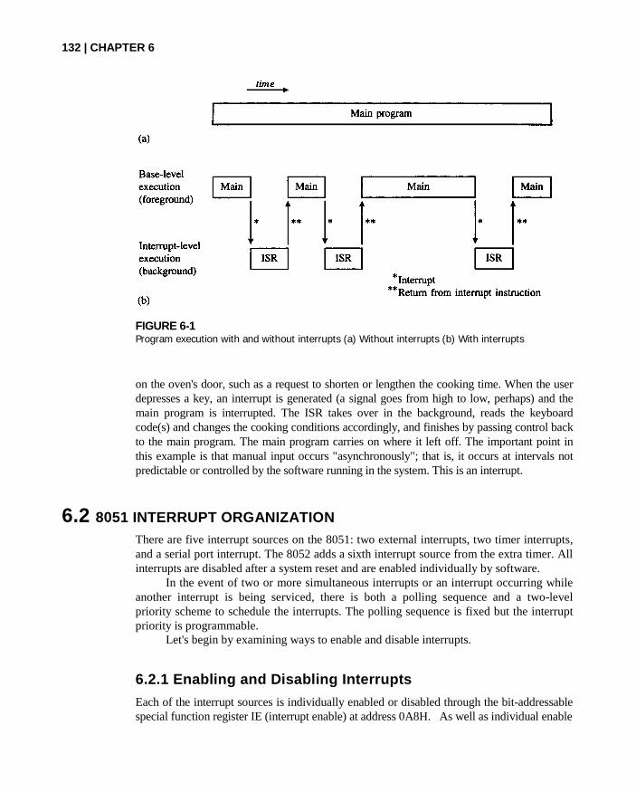
132 | CHAPTER 6
FIGURE 6-1Program execution with and without interrupts (a) Without interrupts (b) With interrupts
on the oven's door, such as a request to shorten or lengthen the cooking time. When the userdepresses a key, an interrupt is generated (a signal goes from high to low, perhaps) and themain program is interrupted. The ISR takes over in the background, reads the keyboardcode(s) and changes the cooking conditions accordingly, and finishes by passing control backto the main program. The main program carries on where it left off. The important point inthis example is that manual input occurs "asynchronously"; that is, it occurs at intervals notpredictable or controlled by the software running in the system. This is an interrupt.
6.2 8051 INTERRUPT ORGANIZATION
There are five interrupt sources on the 8051: two external interrupts, two timer interrupts,and a serial port interrupt. The 8052 adds a sixth interrupt source from the extra timer. Allinterrupts are disabled after a system reset and are enabled individually by software.
In the event of two or more simultaneous interrupts or an interrupt occurring whileanother interrupt is being serviced, there is both a polling sequence and a two-levelpriority scheme to schedule the interrupts. The polling sequence is fixed but the interruptpriority is programmable.
Let's begin by examining ways to enable and disable interrupts.
6.2.1 Enabling and Disabling Interrupts
Each of the interrupt sources is individually enabled or disabled through the bit-addressablespecial function register IE (interrupt enable) at address 0A8H. As well as individual enable

INTERRUPTS | 133
TABLE 6-1IE (interrupt enable) register summary
bits for each interrupt source, there is a global enable/disable bit that is cleared to disableall interrupts or set to turn on interrupts. (See Table 6-1.)
Two bits must be set to enable any interrupt: the individual enable bit and the globalenable bit. For example, timer 1 interrupts are enabled as follows:
SETB ET1 ;ENABLE Timer 1 INTERRUPT
SETB EA ;SET GLOBAL ENABLE BIT
This could also be coded as
MOV IE,#10001000B
Although these two approaches have exactly the same effect following a system reset, theeffect is different if IE is written "on-the-fly" in the middle of a program. The firstapproach has no effect on the other five bits in the IE register, whereas the second approachexplicitly clears the other bits. It is fine to initialize IE with a "move byte" instruction at thebeginning of a program (i.e., following a power-up or system reset), but enabling anddisabling interrupts on-the-fly within a program should use "set bit" and "clear bit"instructions to avoid side effects with other bits in the IE register.
6.2.2 Interrupt Priority
Each interrupt source is individually programmed to one of two priority levels through thebit-addressable special function register IP (interrupt priority) at address 0B8H. (SeeTable 6-2.)
IP is cleared after a system reset to place all interrupts at the lower priority level bydefault. The idea of "priorities" allows an ISR to be interrupted by an interrupt if the newinterrupt is of higher priority than the interrupt currently being serviced. This is straight-forward on the 8051, since there are only two priority levels. If a low-priority ISR is exe-cuting when a high-priority interrupt occurs, the ISR is interrupted. A high-priority ISRcannot be interrupted.

134 | CHAPTER 6
TABLE 6-2
IP (interrupt priority) register summary
Bit Symbol Bit Address Description (1 = Higher Level, 0 = Lower Level)
IP.7 — — UndefinedIP.6 — — UndefinedIP.5 PT2 0BDH Priority for Timer 2 interrupt (8052)IP.4 PS 0BCH Priority for serial port interrupt
IP.3 PT1 0BBH Priority for Timer 1 interruptIP.2 PX1 0BAH Priority for external 1 interruptIP.1 PT0 0B9H Priority for Timer 0 interruptIP.0 PX0 0B8H Priority for external 0 interrupt
The main program, executing at base level and not associated with anyinterrupt, can always be interrupted regardless of the priority of the interrupt. Iftwo interrupts of different priorities occur simultaneously, the higher priorityinterrupt will be serviced first.
6.2.3 Polling Sequence
If two interrupts of the same priority occur simultaneously, a fixed polling sequencedetermines which is serviced first. The polling sequence is external 0, Timer 0,external 1, Timer 1, Serial Port, Timer 2.
Figure 6-2 illustrates the five interrupt sources, the individual and globalenable mechanism, the polling sequence, and the priority levels. The state of allinterrupt sources is available through the respective flag bits in the SFRs. Ofcourse, if any interrupt is disabled, an interrupt does not occur, but software canstill test the interrupt flag. The timer and serial port examples in the previous twochapters used the interrupt flags extensively without actually using interrupts.
A serial port interrupt results from the logical OR of a receive interrupt (8052)or a transmit interrupt (TI). Likewise, Timer 2 interrupts are generated by a timeoverflow (TF2) or by the external input flag (EXF2). The flag bits that generateinterrupts are summarized in Table 6-3.
TABLE 6-3
Interrupt flag bits
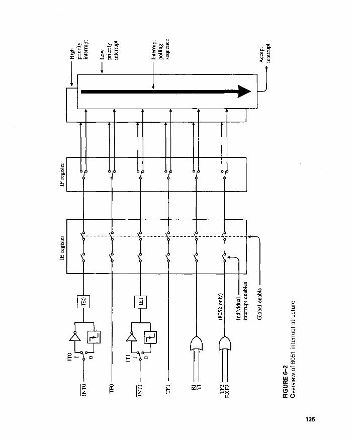

136 | CHAPTER 6
6.3 PROCESSING INTERRUPTS
When an interrupt occurs and is accepted by the CPU, the main program is interrupted.The following actions occur:
The current instruction completes execution. The PC is saved on the stack. The current interrupt status is saved internally. Interrupts are blocked at the level of the interrupt. The PC is loaded with the vector address of the ISR. The ISR executes.
The ISR executes and takes action in response to the interrupt. The ISR finisheswith a RETI (return from interrupt) instruction. This retrieves the old value of the PC fromthe stack and restores the old interrupt status. Execution of the main program continueswhere it left off.
6.3.1 Interrupt Vectors
When an interrupt is accepted, the value loaded into the PC is called the interrupt vector.It is the address of the start of the ISR for the interrupting source. The interrupt vectors aregiven in Table 6-4.
The system reset vector (RST at address 0000H) is included in this table, since, in thissense, it is like an interrupt: it interrupts the main program and loads the PC with a new value.
When "vectoring to an interrupt," the flag that caused the interrupt is automaticallycleared by hardware. The exceptions are RI and TI for serial port interrupts, and TF2 andEXF2 for Timer 2 interrupts. Since there are two possible sources for each of these inter-rupts, it is not practical for the CPU to clear the interrupt flag. These bits must be tested inthe ISR to determine the source of the interrupt, and then the interrupting flag is cleared bysoftware. Usually a branch occurs to the appropriate action, depending on the source ofthe interrupt.
Since the interrupt vectors are at the bottom of code memory, the first instruction ofthe main program is often a jump above this area of memory, such as LJMP 0030H.
TABLE 6-4
Interrupt vectors
Interrupt Flag Vector Address
System resetExternal 0Timer 0External 1Timer 1Serial portTimer 2
RSTIE0TF0IE1TF0RI or TITF2 or EXF2
0000H0003H000BH0013H001BH0023H002BH

INTERRUPTS | 137.
6.4 PROGRAM DESIGN USING INTERRUPTS
The examples in Chapter 3 and Chapter 4 did not use interrupts but made extensive use of"wait loops" to test the timer overflow flags (TF0, TF1, or TF2) or the serial port transmitand receive flags (TI or RI). The problem in this approach is that the CPU's valuable ex-ecution time is fully consumed waiting for flags to be set. This is inappropriate for control-oriented applications where a microcontroller must interact with many input and outputdevices simultaneously.
In this section, examples are developed to demonstrate practical methods for imple-menting software for control-oriented applications. The key ingredient is the interrupt. Al-though the examples are not necessarily bigger, they are more complex, and in recognitionof this, we proceed one step at a time. The reader is advised to follow the examples slowlyand to examine the software meticulously. Some of the most difficult bugs in systemdesigns often involve interrupts. The details must be understood thoroughly.
Since we are using interrupts, the examples will be complete and self-contained. Eachprogram starts at address 0000H with the assumption that it begins execution following asystem reset. The idea is that eventually these programs develop into full-fledged applica-tions that reside in ROM or EPROM.
The suggested framework for a self-contained program using interrupts is shown below.
The first instruction jumps to address 0030H, just above the vector locations wherethe ISRs begin, as given in Table 6-4. As shown in Figure 6-3, the main program begins ataddress 0030H.
6.4.1 Small Interrupt Service Routines
Interrupt service routines must begin near the bottom of code memory at the addressesshown in Table 6-4. Although there are only eight bytes between each interrupt entrypoint, this is often enough memory to perform the desired operation and return from theISR to the main program.
If only one interrupt source was used, say Timer 0, then the following frameworkcould be used:
ORG 0000H ;RESETLJMP MAIN
ORG 000BH ;Timer 0 ENTRY POINT

138 | CHAPTER 6
If more interrupts are used, care must be taken to ensure they start at the correct location(see Table 6-4) and do not overrun the next ISR. Since only one interrupt is used in theexample above, the main program can begin immediately after the RETI instruction.
6.4.2 Large Interrupt Service Routines
If an ISR is longer than eight bytes, it may be necessary to move it elsewhere in codememory or it may trespass on the entry point for the next interrupt. Typically, the ISRbegins with a jump to another area of code memory where the ISR can stretch out.Considering only Timer 0 for the moment, the following framework could be used:
FIGURE 6-3Memory organization when interrupts are used

INTERRUPTS | 139
To keep it simple, our programs will only do one thing at a time initially. The main orforeground program initializes the timer, serial port, and interrupt registers as appropriate,and then does nothing. The work is done totally in the ISR. After the initializeinstructions, the main program consists of the following instruction:
HERE: SJMP HERE
When an interrupt occurs, the main program is interrupted temporarily while theISR executes. The RETI instruction at the end of the ISR returns control to the mainprogram, and it continues doing nothing. This is not as farfetched as one might think. Incontrol-oriented applications, the bulk of the work is in fact done in the interrupt routines.
6.5 TIMER INTERRUPTS
Timer interrupts occur when the timer overflow flag, TFx, is set upon overflow of thetimer registers, THx/TLx. When the 8051 goes to service this interrupt, the timer overflowflag, TFx is automatically cleared by hardware. Therefore, with interrupts enabled, there isno need to explicitly clear TFx in software as was done in Chapter 4 where timers wereused without interrupts.
EXAMPLE Square Wave Using Timer Interrupts
6.1 Write a program using Timer 0 and interrupts to create a 10 kHz square wave on P1.0.
Solution
Discussion
With timer interrupts enabled, the event that generates the interrupt is the setting of thetimer flag, TFx, upon overflow of the timer registers, THx/TLx. This example appears inChapter 4 without using interrupts. The bulk of the program is the same except it is noworganized into the framework for interrupts.
The solution is a complete program. It could be burned into EPROM and installed inan 8051 single-board computer for execution. Immediately after reset, the program counteris loaded with 0000H. The first instruction executed is LJMP MAIN, which branches overthe timer ISR to address 0030H in code memory. The next three instructions (lines 11-13)

140 | CHAPTER 6
initialize Timer 0 for 8-bit auto-reload mode with overflows every 50 µs. The MOV instruc-tion in line 14 enables Timer 0 interrupts, so each overflow of the timer generates an interrupt.Of course, the first overflow will not occur for 50 µs, so the main program falls through to the"do-nothing" loop. Each 50 µs an interrupt occurs; the main program is interrupted and theTimer 0 ISR executes. The ISR simply complements the port bit (line 8) and returns to themain program (line 9) where the do-nothing loop executes for another 50 µs.
Note that the timer flag, TF0, is not explicitly cleared by software. When interruptsare enabled, TF0 is automatically cleared by hardware when the CPU services theinterrupt.
Since the solution is a "complete" program, we must be aware of how the stack isoperating. The return address for the ISR is the location of the SJMP instruction. Thisaddress is pushed on the 8051's internal stack prior to vectoring to the interrupt and ispopped from the stack when the RETI instruction executes (line 9). Since the SP was notinitialized, it defaults to the reset value of 07H. The push operation leaves the returnaddress in internal RAM locations 08H (PCH) and 09H (PCL).
EXAMPLE Two Square Waves Using Interrupts6.2 Write a program using interrupts to simultaneously create 7 kHz and 500 Hz square
waves on P1.7 and P1.6.
SolutionThe hardware configuration with the timings for the desired waveforms is shown in Figure6-4.
This combination of outputs would be extremely difficult to generate on a non-inter-rupt-driven system. Timer 0, providing synchronization for the 7 kHz signal, operates inmode 2, as in the previous example; and timer 1, providing synchronization for the 500 Hzsignal, operates in mode 1, 16-bit timer mode. Since 500 Hz requires a high-time of 1 ms
FIGURE 6-4Waveform example

INTERRUPTS | 141
and low-time of 1 ms, mode 2 cannot be used. (Recall that 256 ms is the maximum timedinterval in mode 2 when the 8051 is operating at 12 MHz.) Here's the program:
Discussion
Again, the framework is for a complete program that could be installed in EPROM orROM on an 8051-based product. The main program and the ISRs are located above the
vector locations for the system reset and interrupts. Both waveforms are created by
"CPL bit" instructions; however, the timed intervals necessitate a slightly different
approach for each.
Since the TL1/TH1 registers must be reloaded after each overflow (i.e., after each in-
terrupt), Timer 1 ISR (a) stops the timer, (b) reloads TL1/TH1, (c) starts the timer, and then
(d) complements the port bit. Note also that TL1/TH1 are not initialized at the beginning of
the main program, unlike TH0. Since TL1/TH1 must be reinitialized after each overflow, TF1is set in the main program by software to "force" an initial interrupt as soon as interrupts are
turned on. This effectively gets the 500 Hz waveform started.
The Timer 0 ISR, as in the previous example, simply complements the port bit andreturns to the main program. SJMP $ is used in the main program as the abbreviated form ofHERE: SJMP HERE. The two forms are functionally equivalent. (See "Special AssemblerSymbols" in Chapter 7.)

142 | CHAPTER 6
6.6 SERIAL PORT INTERRUPTS
Serial port interrupts occur when either the transmit interrupt flag (TI) or the receive inter-rupt flag (RI) is set. A transmit interrupt occurs when transmission of the previouscharacter written to SBUF has finished. A receive interrupt occurs when a character hasbeen completely received and is waiting in SBUF to be read.
Serial port interrupts are slightly different from timer interrupts. The flag that causesa serial port interrupt is not cleared by hardware when the CPU vectors to the interrupt.The reason is that there are two sources for a serial port interrupt, TI or RI. The source ofthe interrupt must be determined in the ISR and the interrupting flag cleared by software.Recall that with timer interrupts the interrupting flag is cleared by hardware when theprocessor vectors to the ISR.
EXAMPLE Character Output Using Interrupts6.3 Write a program using interrupts to continually transmit the ASCII code set (excluding
control codes) to a terminal attached to the 8051's serial port.
Solution
There are 128 7-bit codes in the ASCII chart. (See Appendix F.) These consist of 95 graphiccodes (20H to 7EH) and 33 control codes (00H to 1FH, and 7FH). The program shown belowis self-contained and executable from EPROM or ROM immediately after a system reset.
D
At
iscussion
fter jumping to MAIN at code address 0030H, the first three instructions initialize Timer 1
o provide a 1200 baud clock to the serial port (lines 10-12). MOV SCON,#42H initializes
INTERRUPTS | 143
the serial port for mode 1 (8-bit UART) and sets the TI flag to force an interrupt as soon asinterrupts are enabled. Then, the first ASCII graphic code (20H) is loaded into A andserial port interrupts are enabled. Finally, the main body of the program enters a do-nothing loop (SJMP $).
The serial port interrupt service routine does all the work once the main programsets up initial conditions. The first two instructions check the accumulator, and if theASCII code has reached 7FH (i.e., the last code transmitted was 7EH), reset theaccumulator to 20H (lines 19-20). Then, the ASCII code is sent to the serial port buffer(MOV SBUF,A), the code is incremented (INC A), the transmit interrupt flag is cleared(CLR TI), and the ISR is terminated (RETI). Control returns to the main program andSJMP $ executes until TI is set at the end of the next character transmission.
If we compare the CPU's speed to the rate of character transmission, we see thatSJMP $ executes for a very large percentage of the time for this program. What is this per-centage? At 1200 baud, each bit transmitted takes 11200 = 0.833 ms. Eight data bits plus astart-and-stop bit, therefore, take 8.33 ms or 8333 µs. The worst-case execution time for theSPJSR is found by totaling the number of cycles for each instruction and multiplying by 1µs (assuming 12 MHz operation). This turns out to be 8 µs. So, of the 8333 µs for eachcharacter transmission, only 8 µs are for the interrupt service routine. The SJMP $instruction executes about 8325 8333 x 100 = 99.90% of the time. Since interrupts areused, the SJMP $ instruction could be replaced with other instructions performing othertasks required in the application. Interrupts would still occur every 8.33 ms, and characterswould still be transmitted out the serial port as they are in the above program.
6.7 EXTERNAL INTERRUPTS
External interrupts occur as a result of a low-level or negative edge on the INT0 or INT1pin on the 8051 IC. These are the alternate functions for Port 3 bits P3.2 (pin 12) and P3.3(pin 13), respectively.
The flags that actually generate these interrupts are bits IE0 and IE1 in TCON.When an external interrupt is generated, the flag that generated it is cleared by hardwarewhen vectoring to the ISR only if the interrupt was transition-activated. If the interruptwas level-activated, then the external requesting source controls the level of the requestflag, rather than the on-chip hardware.
The choice of low-level-activated interrupts versus negative-edge-activated interruptsis programmable through the IT0 and IT1 bits in TCON. For example, if IT1 = 0, externalinterrupt 1 is triggered by a detected low at the INT1 pin. If IT1 = 1, external interrupt 1 isedge-triggered. In this mode, if successive samples of the INT1 pin show a high in onecycle and a low in the next, the interrupt request flag IE1 in ICON is set. Flag bit IE1 thenrequests the interrupt.
Since the external interrupt pins are sampled once each machine cycle, an inputshould be held for at least 12 oscillator periods to ensure proper sampling. If the externalinterrupt is transition-activated, the external source must hold the request pin high for atleast one cycle and then hold it low for at least one more cycle to ensure the transition isdetected. IE0 and IE1 are automatically cleared when the CPU vectors to the interrupt.

144 | CHAPTER 6
If the external interrupt is level-activated, the external source must hold the requestactive until the requested interrupt is actually generated. Then it must deactivate therequest before the interrupt service routine is completed, or another interrupt will begenerated. Usually, an action taken in the ISR causes the requesting source to return theinterrupting signal to the inactive state.
EXAMPLE Furnace Controller6.4 Using interrupts, design an 8051 furnace controller that keeps a building at 20°C ± 1°C.
Solution
The following interface is assumed for this example. The furnace ON/OFF solenoid isconnected to P1.7 such that
P1.7 = 1 for solenoid engaged (furnace ON)P1.7 = 0 for solenoid disengaged (furnace OFF)
Temperature sensors are connected to INT0 and INT1 and provide HOT and COLD
signals, respectively, such that
HOT = 0 if T> 21°CCOLD = 0 if T< 19°C
The program should turn on the furnace for T < 19°C and turn it off for T > 21°C. Thehardware configuration and a timing diagram are shown in Figure 6-5.
Discussion
The first three instructions in the main program (lines 14-16) turn on external interrupts and
make both INT0 and INT1 negative-edge triggered. Since the current state of the HOT
(P3.3) and COLD (P3.3) inputs is not known, the next three instructions (lines 17-19) are
required to turn the furnace ON or OFF, as appropriate. First, the furnace is turned ON

INTERRUPTS | 145
FIGURE 6-5Furnace example. (a) Hardware connections (b) Timing
(SETB P1.7), and then the HOT input is sampled (JB P3.2,SKIP). If HOT is high, then T< 21°C, so the next instruction is skipped and the furnace is left ON. If, however, HOT islow, then T > 21°C. In this case the jump does not take place. The next instruction turnsthe furnace OFF (CLR P1.7) before entering the do-nothing loop.
Once everything is set up properly in the main program, little remains to be done.Each time the temperature rises above 21°C or falls below 19°C, an interrupt occurs. TheISRs simply turn the furnace ON (SETB P1.7) or OFF (CLR P1.7), as appropriate, andreturn to the main program.
Note that an ORG 0003H statement is not necessary immediately before theEX0ISR label. Since the LJMP MAIN instruction is three bytes long, EX0ISR is certain tostart at 0003H, the correct entry point for external 0 interrupts.
EXAMPLE Intrusion Warning System6.5 Design an intrusion warning system using interrupts that sounds a 400 Hz tone for 1
second (using a loudspeaker connected to P1.7) whenever a door sensor connected toINT0 makes a high-to-low transition.

146 | CHAPTER 6
FIGURE 6-6
Loudspeaker interface using interrupts (a) Hardware connections (b) Timing
Solution
The solution to this example uses three interrupts: external 0 (door sensor), Timer 0 (1second timeout), and Timer 1 (400 Hz tone). The hardware configuration and timings areshown in Figure 6-6.

INTERRUPTS | 147
Discussion
This is our largest program thus far. Five distinct sections are the interrupt vector locations, the
main program, and the three interrupt service routines. All vector locations contain LJMP
instructions to the respective routines. The main program, starting at code address 0030H,
contains only four instructions. SETB IT0 configures the door sensing interrupt input as
negative-edge triggered. MOV TMOD,#11H configures both timers for mode 1, 16-bit timer
mode. Only the external 0 interrupt is enabled initially (MOV IE,#81H), so a "door-open"
condition is needed before any interrupt is accepted. Finally, SJMP $ puts the main program in
a do-nothing loop.
When a door-open condition is sensed (by a high-to-low transition of INT0 ), an
external 0 interrupt is generated, EX0ISR begins by putting the constant 20 in R7 (see
below), then sets the overflow flags for both timers to force timer interrupts to occur.
Timer interrupts will only occur, however, if the respective bits are enabled in the IEregister. The next two instructions (SETB ET0 and SETB ET1) enable timer interrupts. Finally,
EX0ISR terminates with a RETI to the main program.
Timer 0 creates the 1 second timeout, and Timer 1 creates the 400 Hz tone. After
EX0ISR returns to the main program, timer interrupts are immediately generated (and
accepted after one execution of SJMP $). Because of the fixed polling sequence (see
Figure 6-2), the Timer 0 interrupt is serviced first. A 1 second timeout is created by pro-
gramming 20 repetitions of a 50,000 s timeout. R7 serves as the counter. Nineteen
times out of 20, T0ISR operates as follows. First, Timer 0 is turned off and R7 is decre-
mented. Then, TH0/TL is reloaded with -50,000, the timer is turned back on, and the
interrupt is terminated. On the 20th Timer 0 interrupt, R7 is decremented to 0 (1 second
has elapsed). Both timer interrupts are disabled (CLR ET0, CLR ET1) and the interrupt
is terminated. No further timer interrupts will be generated until the next "door-open"
condition is sensed.

148 | CHAPTER 6
FIGURE 6-7
Sampling of interrupts on S5P2
The 400 Hz tone is programmed using Timer 1 interrupts, 400 Hz requires a period of1/400 = 2,500 µs or 1,250 high-time and 1,25 µs low-time. Each timer 1 ISR simply puts —1250 in TH1/TL1, complements the port bit driving the loudspeaker, then terminates.
6.8 INTERRUPT TIMINGS
Interrupts are sampled and latched on S5P2 of each machine cycle. (See Figure 6-7.) Theyare polled on the next machine cycle, and if an interrupt condition exists, it is accepted if(a) no other interrupt of equal or higher priority is in progress, (b) the polling cycle is thelast cycle in an instruction, and (c) the current instruction is not a RETI or any access toIE or IP. During the next two cycles, the processor pushes the PC on the stack and loadsthe PC with the interrupt vector address. The ISR begins.
The stipulation that the current instruction is not RETI ensures that at least one in-struction executes after each interrupt service routine. The timing is shown in Figure 6-8.
FIGURE 6-8
Polling of interrupts

INTERRUPTS | 149
FIGURE 6-9Interrupt latency
The time between an interrupt condition occurring and the ISR beginning is calledinterrupt latency. Interrupt latency is critical in many control applications. With a 12MHz crystal, the interrupt latency can be as short as 3.25 µs on the 8051. An 8051 systemthat uses one high-priority interrupt will have a worst-case interrupt latency of 9.25 µs (as-suming the high-priority interrupt is always enabled). This occurs if the interrupt conditionhappens just before the RETI of a level 0 ISR that is followed by a multiply instruction(see Figure 6-9).
SUMMARY
This chapter has presented the major details required to embark on the design of interrupt-driven systems with the 805I microcontroller. Readers are advised to begin programmingwith interrupts in increments. The examples in this chapter serve as a good first contactwith 8051 interrupts.
The 8051 single-board computers usually contain a monitor program in EPROMresiding at the bottom of code memory. If interrupts are not used in the monitorprogram, the vector locations probably contain LJMP instructions to an area of CODERAM where user applications are loaded for execution and debugging. Themanufacturer's literature will provide the addresses for programmers to use as entrypoints for interrupt service routines. Alternatively, users can simply "look" in theinterrupt vector locations, using the monitor program's commands for examining codememory locations. The content of code memory address 0003H, for example, willcontain the opcode of the first instruction to execute for an external 0 interrupt. If this isan LJMP opcode (22H: see Appendix B), then the next two addresses (0004H and0005H) contain the address of the ISR, and so on.
Alternately, users can develop self-contained interrupt applications, as shown inthe examples. The object bytes can be burned into EPROM and installed in the targetsystem at code address 000EH. When the system is powered up or reset, the applica-tion begins execution without the need of a monitor program for loading and startingthe application.
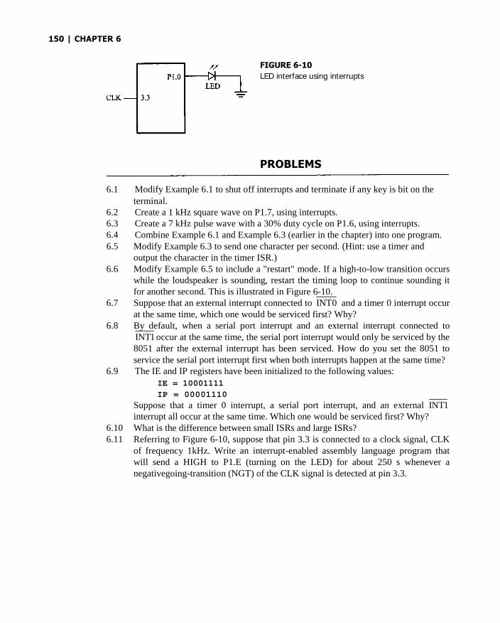
150 | CHAPTER 6
FIGURE 6-10
LED interface using interrupts
PROBLEMS
6.1 Modify Example 6.1 to shut off interrupts and terminate if any key is bit on theterminal.
6.2 Create a 1 kHz square wave on P1.7, using interrupts.6.3 Create a 7 kHz pulse wave with a 30% duty cycle on P1.6, using interrupts.6.4 Combine Example 6.1 and Example 6.3 (earlier in the chapter) into one program.6.5 Modify Example 6.3 to send one character per second. (Hint: use a timer and
output the character in the timer ISR.)6.6 Modify Example 6.5 to include a "restart" mode. If a high-to-low transition occurs
while the loudspeaker is sounding, restart the timing loop to continue sounding itfor another second. This is illustrated in Figure 6-10.
6.7 Suppose that an external interrupt connected to INT0 and a timer 0 interrupt occurat the same time, which one would be serviced first? Why?
6.8 By default, when a serial port interrupt and an external interrupt connected toINT1 occur at the same time, the serial port interrupt would only be serviced by the8051 after the external interrupt has been serviced. How do you set the 8051 toservice the serial port interrupt first when both interrupts happen at the same time?
6.9 The IE and IP registers have been initialized to the following values:IE = 10001111
IP = 00001110
Suppose that a timer 0 interrupt, a serial port interrupt, and an external INT1interrupt all occur at the same time. Which one would be serviced first? Why?
6.10 What is the difference between small ISRs and large ISRs?6.11 Referring to Figure 6-10, suppose that pin 3.3 is connected to a clock signal, CLK
of frequency 1kHz. Write an interrupt-enabled assembly language program thatwill send a HIGH to P1.E (turning on the LED) for about 250 s whenever anegativegoing-transition (NGT) of the CLK signal is detected at pin 3.3.
Assembly LanguageProgramming
7.1 INTRODUCTION
This chapter introduces assembly language programming for the 8051 microcontroller.Assembly language is a computer language lying between the extremes of machine languageand high-level language. Typical high-level languages like Pascal or C use words andstatements that are easily understood by humans, although still a long way from "natural"language. Machine language is the binary language of computers. A machine language pro-gram is a series of binary bytes representing instructions the computer can execute.
Assembly language replaces the binary codes of machine language with easy to re-member "mnemonics" that facilitate programming. For example, an addition instructionin machine language might be represented by the code "10110011." It might berepresented in assembly language by the mnemonic "ADD." Programming withmnemonics is obviously preferable to programming with binary codes.
Of course, this is not the whole story. Instructions operate on data, and the locationof the data is specified by various "addressing modes" embedded in the binary code of themachine language instruction. So, there may be several variations of the ADD instruction,depending on what is added. The rules for specifying these variations are central to thetheme of assembly language programming.
An assembly language program is not executable by a computer. Once written, theprogram must undergo translation to machine language. In the example above, themnemonic "ADD" must be translated to the binary code "10110011." Depending on thecomplexity of the programming environment, this translation may involve one or moresteps before an executable machine language program results. As a minimum, a programcalled an "assembler" is required to translate the instruction mnemonics to machinelanguage binary codes. A further step may require a "linker" to combine portions ofprograms from separate files and to set the address in memory at which the program mayexecute. We begin with a few definitions.
151

152 | CHAPTER 7
An assembly language program is a program written using labels, mnemonics, andso on, in which each statement corresponds to a machine instruction. Assembly languageprograms, often called source code or symbolic code, cannot be executed by a computer.
A machine language program is a program containing binary codes that representinstructions to a computer. Machine language programs, often called object code, are exe-cutable by a computer.
An assembler is a program that translates an assembly language program into a ma-chine language program. The machine language program (object code) may be in"absolute" form or in "relocatable" form. In the latter case, "linking" is required to set theabsolute address for execution.
A linker is a program that combines relocatable object programs (modules) and pro-duces an absolute object program that is executable by a computer. A linker is sometimescalled a "linker/locator" to reflect its separate functions of combining relocatable modules(linking) and setting the address for execution (locating).
A segment is a unit of code or data memory. A segment may be relocatable or ab-solute. A relocatable segment has a name, type, and other attributes that allow the linker tocombine it with other partial segments, if required, and to correctly locate the segment. Anabsolute segment has no name and cannot be combined with other segments.
A module contains one or more segments or partial segments. A module has a nameassigned by the user. The module definitions determine the scope of local symbols. Anobject file contains one or more modules. A module may be thought of as a "file" in manyinstances.
A program consists of a single absolute module, merging all absolute andrelocatable segments from all input modules. A program contains only the binary codesfor instructions (with addresses and data constants) that are understood by a computer.
7.2 ASSEMBLER OPERATION
There are many assembler programs and other support programs available to facilitate thedevelopment of applications for the 8051 microcontroller. Intel's original MCS-51TM
family assembler, ASM51TM, is no longer available commercially. However, it set thestandard to which the others are compared. In this chapter, we focus on assembly languageprogramming as undertaken using the most common features of ASM51. Although manyfeatures are standardized, some may not be implemented in assemblers from othercompanies.
ASM51 is a powerful assembler with all the bells and whistles. It is available on Inteldevelopment systems and on the IBM PC family of microcomputers. Since these "host"computers contain a CPU chip other than the 8051, ASM51 is called a cross assembler. An8051 source program may be written on the host computer (using any text editor) and maybe assembled to an object file and listing file (using ASM51), but the program may not beexecuted. Since the host system's CPU chip is not an 8051, it does not understand the binaryinstructions in the object file. Execution on the host computer requires either hardware e-mulation or software simulation of the target CPU. A third possibility is to download theobject program to an 8051-based target system for execution. Hardware emulation, softwaresimulation, downloading, and other development techniques are discussed in Chapter 10.

ASSEMBLY LANGUAGE PROGRAMMING | 153
ASM51 is invoked from the system prompt by
ASM51 source file [assembler controls]
The source file is assembled and any assembler controls specified take effect. (Assemblercontrols, which are optional, are discussed later in this chapter.) The assembler receives asource file as input (e.g., PROGRAM.SRC) and generates an object file(PROGRAM.OBJ) and listing file (PROGRAM .LST) as output. This is illustrated inFigure 7-1.
Since most assemblers scan the source program twice in performing the translationto machine language, they are described as two-pass assemblers. The assembler uses alocation counter as the address of instructions and the values for labels. The action ofeach pass is described below.
7.2.1 Pass One
During the first pass, the source file is scanned line-by-line and a symbol table isbuilt. The location counter defaults to 0 or is set by the ORG (set origin) directive.As the file is scanned, the location counter is incremented by the length of eachinstruction. Define data directives (DBs or DWs) increment the location counter bythe number of bytes defined. Reserve memory directives (DSs) increment thelocation counter by the number of bytes reserved.
Each time a label is found at the beginning of a line, it is placed in the symbol tablealong with the current value of the location counter. Symbols that are defined using equatedirectives (EQUs) are placed in the symbol table along with the "equated" value. The sym-bol table is saved and then used during pass two.
7.2.2 Pass Two
During pass two, the object and listing files are created. Mnemonics are converted to op-codes and placed in the output files. Operands are evaluated and placed after the instruction
opcodes. Where symbols appear in the operand field, their values are retrieved from the
FIGURE 7-1
Assembling a source program
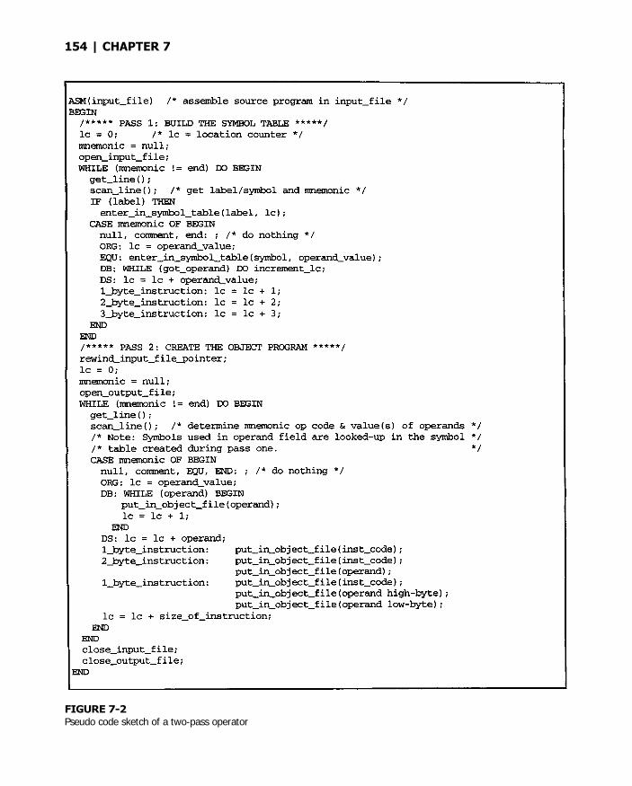
154 | CHAPTER 7
FIGURE 7-2Pseudo code sketch of a two-pass operator
ASSEMBLY LANGUAGE PROGRAMMING | 155
symbol table (created during pass one) and used in calculating the correct data oraddresses for the instructions.
Since two passes are performed, the source program may use "forward references,"that is, use a symbol before it is defined. This would occur, for example, in branchingahead in a program.
The object file, if it is absolute, contains only the binary bytes (00H-0FFH) of themachine language program. A relocatable object file will also contain a symbol table andother information required for linking and locating. The listing file contains ASCII textcodes (20H-7EH) for both the source program and the hexadecimal bytes in the machinelanguage program.
A good demonstration of the distinction between an object file and a listing file is todisplay each on the host computer's CRT display (using, for example, the TYPE commandon MS-DOS systems). The listing file clearly displays, with each line of output containingan address, opcode, and perhaps data, followed by the program statement from the sourcefile. The listing file displays properly because it contains only ASCII text codes. Display-ing the object file is a problem, however. The output will appear as "garbage," since theobject file contains binary codes of an 8051 machine language program, rather than ASCIItext codes.
In Figure 7-2, a sketch of a two-pass assembler is shown written in a pseudo com-puter language (similar to Pascal or C) to enhance readability.
7.3 ASSEMBLY LANGUAGE PROGRAM FORMAT
Assembly language programs contain the following:
Machine instructions Assembler directives Assembler controls Comments
Machine instructions are the familiar mnemonics of executable instructions (e.g.,ANL). Assembler directives are instructions to the assembler program that define programstructure, symbols, data, constants, and so on (e.g., ORG). Assembler controls set assem-bler modes and direct assembly flow (e.g., $TITLE). Comments enhance the readability ofprograms by explaining the purpose and operation of instruction sequences.
Those lines containing machine instructions or assembler directives must be writtenfollowing specific rules understood by the assembler. Each line is divided into "fields"separated by space or tab characters. The general format for each line is as follows:
[label:] mnemonic [operand] [,operand] [.. .] [;comment]
Only the mnemonic field is mandatory. Many assemblers require the label field, if present,to begin on the left in column 1, and subsequent fields to be separated by space or tabcharacters. With ASM51, the label field needn't begin in column 1 and the mnemonic fieldneedn't be on the same line as the label field. The operand field must, however, begin onthe same line as the mnemonic field. The fields are described below.

156 | CHAPTER 7
7.3.1 Label Field
A label represents the address of the instruction (or data) that follows. When branching tothis instruction, this label is used in the operand field of the branch or jump instruction(e.g., SJMP SKIP).
Whereas the term "label" always represents an address, the term "symbol" is moregeneral. Labels are one type of symbol and are identified by the requirement that they mustterminate with a colon (:). Symbols are assigned values or attributes, using directives suchas EQU, SEGMENT, BIT, DATA, etc. Symbols may be addresses, data constants, namesof segments, or other constructs conceived by the programmer. Symbols do not terminatewith a colon. In the example below, PAR is a symbol and START is a label (which is atype of symbol).
PAR EQU 500 ;"PAR" IS A SYMBOL WHICH;REPRESENTS THE VALUE 500
START: MOV A,#0FFH ;"START" IS A LABEL WHICH;REPRESENTS THE ADDRESS OF;THE MOV INSTRUCTION
A symbol (or label) must begin with a letter, question mark, or underscore ( _ ); mustbe followed by letters, digit, "?", or "_"; and can contain up to 31 characters.
1Symbols
may use upper- or lowercase characters, but they are treated the same. Reserved words(mnemonics, operators, predefined symbols, and directives) may not be used.
7.3.2 Mnemonic Field
Instruction mnemonics or assembler directives go into mnemonic field, which follows thelabel field. Examples of instruction mnemonics are ADD, MOV, DIV, or INC. Examplesof assembler directives are ORG, EQU, or DB. Assembler directives are described later inthis chapter.
7.3.3 Operand Field
The operand field follows the mnemonic field. This field contains the address or data used bythe instruction. A label may be used to represent the address of the data, or a symbol may beused to represent a data constant. The possibilities for the operand field are largely dependenton the operation. Some operations have no operand (e.g., the RET instruction), while othersallow for multiple operands separated by commas. Indeed, the possibilities for the operandfield are numerous, and we shall elaborate on these at length. But first, the comment field.
7.3.4 Comment Field
Remarks to clarify the program go into comment field at the end of each line. Commentsmust begin with a semicolon (;). Entire lines may be comment lines by beginning them with
1The reader is reminded that the rules specified in this chapter apply to Intel's ASM51. Other assemblers may
have different requirements.
ASSEMBLY LANGUAGE PROGRAMMING | 157
a semicolon. Subroutines and large sections of a program generally begin with a commentblock—several lines of comments that explain the general properties of the section of soft-ware that follows.
7.3.5 Special Assembler Symbols
Special assembler symbols are used for the register-specific addressing modes. These in-clude A, R0 through R7, DPTR, PC, C, and AB. In addition, a dollar sign ($) can be usedto refer to the current value of the location counter. Some examples follow.
SETB CINC DPTRJNB TI,$
The last instruction above makes effective use of ASM51's location counter to avoid usinga label. It could also be written as
HERE: JNB TI,HERE
7.3.6 Indirect Address
For certain instructions, the operand field may specify a register that contains the addressof the data. The commercial "at" sign (@) indicates address indirection and may only beused with R0, R1, the DPTR, or the PC, depending on the instruction. For example,
ADD A,@R0MOVC A,@A+PC
The first instruction above retrieves a byte of data from internal RAM at the address spec-ified in R0. The second instruction retrieves a byte of data from external code memory atthe address formed by adding the contents of the accumulator to the program counter.Note that the value of the program counter, when the add takes place, is the address of theinstruction following MOVC. For both instructions above, the value retrieved is placedinto the accumulator.
7.3.7 Immediate Data
Instructions using immediate addressing provide data in the operand field that becomepart of the instruction. Immediate data are preceded with a pound sign ( # ). For example,
CONSTANT EQU 100MOV A,#0FEHORL 40H,#CONSTANT
All immediate data operations (except MOV DPTR,#data) require eight bits of data. Theimmediate data are evaluated as a 16-bit constant, and then the low-byte is used. All bits in

158 | CHAPTER 7
the high-byte must be the same (00H or 0FFH) or the error message "value will not fit in abyte" is generated. For example, the following instructions are syntactically correct:
MOV A,#0FF00HMOV A,#00FFH
But the following two instructions generate error messages:
MOV A,#0FE00HMOV A,#01FFH
If signed decimal notation is used, constants from -256 to +255 may also be used.For example, the following two instructions are equivalent (and syntactically correct):
MOV A,#-256MOV A,#0FF00H
Both instructions above put 00H into accumulator A.
7.3.8 Data Address
Many instructions access memory locations using direct addressing and require an on-chipdata memory address (00H to 7FH) or an SFR address (80H to 0FFH) in the operand field.Predefined symbols may be used for the SFR addresses. For example,
MOV A,45HMOV A,SBUF ;SAME AS MOV A,99H
7.3.9 Bit Address
One of the most powerful features of the 8051 is the ability to access individual bits with-out the need for masking operations on bytes. Instructions accessing bit-addressable loca-tions must provide a bit address in internal data memory (00H to 7FH) or a bit address inthe SFRs (80H to 0FFH).
There are three ways to specify a bit address in an instruction: (a) explicitly by giv-ing the address, (b) using the dot operator between the byte address and the bit position,and (c) using a predefined assembler symbol. Some examples follow.
SETB 0E7H ;EXPLICIT BIT ADDRESSSETB ACC.7 ;DOT OPERATOR (SAME AS ABOVE)JNB TI,$ ;"TI" IS A PRE-DEFINED SYMBOLJNB 99H,$ ;(SAME AS ABOVE)
7.3.10 Code Address
A code address is used in the operand field for jump instructions, including relative jumps(SJMP and conditional jumps), absolute jumps and calls (ACALL, AJMP), and long jumpsand calls (LJMP, LCALL).

ASSEMBLY LANGUAGE PROGRAMMING | 159
The code address is usually given in the form of a label. For example,
HERE:
SJMP HERE
ASM51 will determine the correct code address and insert into the instruction the correct8-bit signed offset, 11-bit page address, or 16-bit long address, as appropriate.
7.3.11 Generic Jumps and Calls
ASM51 allows programmers to use a generic JMP or CALL mnemonic. "JMP" can beused instead of SJMP, AJMP or LJMP; and "CALL" can be used instead of ACALL orLCALL. The assembler converts the generic mnemonic to a "real" instruction following afew simple rules. The generic mnemonic converts to the short form (for JMP only) if noforward references are used and the jump destination is within -128 locations, or to theabsolute form if no forward references are used and the instruction following the JMP orCALL instruction is in the same 2 K block as the destination instruction. If short orabsolute forms cannot be used, the conversion is to the long form.
The conversion is not necessarily the best programming choice. For example, ifbranching ahead a few instructions, the generic JMP will always convert to LJMP eventhough an SJMP is probably better. Consider the assembled instruction sequence in Figure7-3 using three generic jumps. The first jump (line 3) assembles as SJMP because thedestination is before the jump (i.e., no forward reference) and the offset is less than -128.The ORG directive in line 4 creates a gap of 200 locations between the label START andthe second jump, so the conversion on line 5 is to AJMP because the offset is too great forSJMP. Note also that the address following the second jump (12FEH) and the address ofSTART (1234H) are within the same 2K page, which, for this instruction sequence, isbounded by 1000H and 17FFH. This criterion must be met for absolute addressing. Thethird jump assembles as LJMP because the destination (FINISH) is not yet defined when
FIGURE 7-3Use of the generic JMP mnemonic

160 | CHAPTER 7
the jump is assembled (i.e., a forward reference is used). The reader can verify that the con-version is as stated by examining the object field for each jump instruction. Verify the hexa-decimal codes with those found in Appendix C for SJMP, AJMP, and LJMP.
7.4 ASSEMBLE-TIME EXPRESSION EVALUATION
Values and constants in the operand field may be expressed three ways: (a) explicitly(e.g., 0EFH), (b) with a predefined symbol (e.g., ACC), or (c) with an expression (e.g., 2+ 3). The use of expressions provides a powerful technique for making assembly languageprograms more readable and more flexible. When an expression is used, the assemblercalculates a value and inserts it into the instruction.
All expression calculations are performed using 16-bit arithmetic; however, either 8or 16 bits are inserted into the instruction as needed. For example, the following two in-structions are the same:
MOV DPTR,#04FFH + 3MOV DPTR,#0502H ;ENTIRE 16-BIT RESULT USED
If the same expression is used in a "MOV A,#data" instruction, however, the errormessage "value will not fit in a byte" is generated by ASM51. An overview of the rulesfor evaluating expressions follows.
7.4.1 Number Bases
The base for numeric constants is indicated in the usual way for Intel microprocessors.Constants must be followed with "B" for binary, "0" or "Q" for octal, "D" or nothing fordecimal, or "H" for hexadecimal. For example, the following instructions are the same:
MOV A,#15
MOV A,#1111BMOV A,#0FHMOV A,#17QMOV A,#15D
Note that a digit must be the first character for hexadecimal constants in order to differen-tiate them from labels (i.e., "0A5H" not "A5H").
7.4.2 Character Strings
Strings using one or two characters may be used as operands in expressions. The ASCIIcodes are converted to the binary equivalent by the assembler. Character constants areenclosed in single quotes 0. Some examples follow.
CJNE A,#'Q',AGAINSUBB A,#'0' ;CONVERT ASCII DIGIT TO
;BINARY DIGITMOV DPTR,#'AB'MOV DPTR,#4142H ;SAME AS ABOVE

ASSEMBLY LANGUAGE PROGRAMMING | 161
7.4.3 Arithmetic Operators
The arithmetic operators are
+ addition
- subtraction* multiplication
/ divisionMOD modulo (remainder after division)
For example, the following two instructions are the same:
MOV A,10+10HMOV A,#1AH
The following two instructions are also the same:
MOV A,#25 MOD 7MOV A,#4
Since the MOD operator could be confused with a symbol, it must be separated from itsoperands by at least one space or tab character, or the operands must be enclosed in paren-theses. The same applies for the other operators composed of letters.
7.4.4 Logical Operators
The logical operators are
OR logical ORAND logical ANDXOR logical Exclusive ORNOT logical NOT (complement)
The operation is applied on the corresponding bits in each operand. The operator must beseparated from the operands by space or tab characters. For example, the following twoinstructions are the same:
MOV A,#'9' AND 0FHMOV A,#9
The NOT operator only takes one operand. The following three MOV instructions are thesame:
THREE EQU 3MINUS_THREE EQU -3
MOV A,#(NOT THREE)+1MOV A,#MINUS_THREEMOV A,#11111101B

162 | CHAPTER 7
7.4.5 Special Operators
The special operators are
SHR shift rightSHL shift leftHIGH high-byteLOW low-byte
() evaluate first
For example, the following two instructions are the same:
MOV A,#8 SHL 1MOV A,#12H
The following two instructions are also the same:
MOV A,#HIGH 1234HMOV A,#12H
7.4.6 Relational Operators
When a relational operator is used between two operands, the result is always false(0000H) or true (0FFFFH). The operators are
E Q = e q u a l sNE <> not equalsLT < less thanLE <= less than or equal toGT > greater thanGE >= greater than or equal to
Note that for each operator, two forms are acceptable (e.g., "EQ" or "="). In the followingexamples, all relational tests are "true":
MOV A,#5 = 5MOV A,#5 NE 4MOV A,#'X' LT 'Z'MOV A,#'X' >= 'X'MOV A,#$ > 0
MOV A,#100 GE 50
So, the assembled instructions are all equal to
MOV A,#0FFH
Even though expressions evaluate to 16-bit results (i.e., 0FFFFH), in the examples aboveonly the low-order eight bits are used, since the instruction is a move byte operation. Theresult is not considered too big in this case, because as signed numbers the 16-bit value0FFFFH and the 8-bit value 0FFH are the same ( -1).
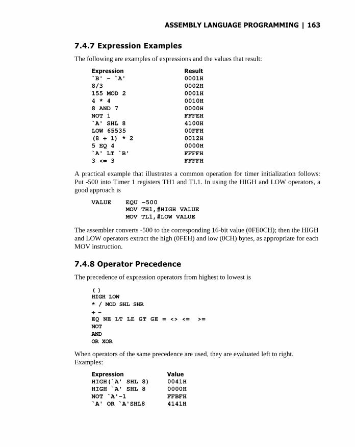
ASSEMBLY LANGUAGE PROGRAMMING | 163
7.4.7 Expression Examples
The following are examples of expressions and the values that result:
Expression Result
`B' - `A' 0001H8/3 0002H155 MOD 2 0001H4 * 4 0010H8 AND 7 0000HNOT 1 FFFEH`A' SHL 8 4100HLOW 65535 00FFH(8 + 1) * 2 0012H5 EQ 4 0000H`A' LT `B' FFFFH3 <= 3 FFFFH
A practical example that illustrates a common operation for timer initialization follows:Put -500 into Timer 1 registers TH1 and TL1. In using the HIGH and LOW operators, agood approach is
VALUE EQU -500MOV TH1,#HIGH VALUEMOV TL1,#LOW VALUE
The assembler converts -500 to the corresponding 16-bit value (0FE0CH); then the HIGHand LOW operators extract the high (0FEH) and low (0CH) bytes, as appropriate for eachMOV instruction.
7.4.8 Operator Precedence
The precedence of expression operators from highest to lowest is
( )HIGH LOW* / MOD SHL SHR
+ -EQ NE LT LE GT GE = <> <= >=NOTANDOR XOR
When operators of the same precedence are used, they are evaluated left to right.Examples:
Expression ValueHIGH(`A' SHL 8) 0041HHIGH `A' SHL 8 0000HNOT `A'-1 FFBFH`A' OR `A'SHL8 4141H
164 | CHAPTER 7
7.5 ASSEMBLER DIRECTIVES
Assembler directives are instructions to the assembler program. They are not assemblylanguage instructions executable by the target microprocessor. However, they are placedin the mnemonic field of the program. With the exception of DB and DW, they have nodirect effect on the contents of memory.
ASM51 provides several categories of directives:
Assembler state control (ORG, END, USING) Symbol definition (SEGMENT, EQU, SET, DATA, IDATA, XDATA, BIT, CODE) Storage initialization/reservation (DS, DBIT, DB, DW) Program linkage (PUBLIC, EXTRN, NAME) Segment selection (RSEG, CSEG, DSEG, ISEG, ESEG, XSEG)
Each assembler directive is presented below, ordered by category.
7.5.1 Assembler State Control
7.5.1.1 ORG (Set Origin) The format for the ORG (set origin) directive is
ORG expression
The ORG directive alters the location counter to set a new program origin for statementsthat follow. A label is not permitted. Two examples follow.
ORG 100H ;SET LOCATION COUNTER TO 100HORG ($ + 1000H) AND 0F000H ;SET TO NEXT 4K BOUNDARY
The ORG directive can be used in any segment type. If the current segment is absolute,the value will be an absolute address in the current segment. If a relocatable segment isactive, the value of the ORG expression is treated as an offset from the base address of thecurrent instance of the segment.
7.5.1.2 End The format for the END directive is
END
END should be the last statement in the source file. No label is permitted and nothing be-yond the END statement is processed by the assembler.
7.5.1.3 Using The format for the USING directive is
USING expression
This directive informs ASM51 of the currently active register bank. Subsequent uses ofthe predefined symbolic register addresses AR0 to AR7 will convert to the appropriatedirect address for the active register bank. Consider the following sequence:
USING 3PUSH AR7
ASSEMBLY LANGUAGE PROGRAMMING | 165
USING 1PUSH AR7
The first push above assembles to PUSH 1FH (R7 in bank 3), whereas the second pushassembles to PUSH 0FH (R7 in bank 1).
Note that USING does not actually switch register banks; it only informs ASM51 ofthe active bank. Executing 8051 instructions is the only way to switch register banks. Thisis illustrated by modifying the example above as follows:
MOV PSW,#00001000B ;SELECT REGISTER BANK 3USING 3
PUSH AR7 ;ASSEMBLE TO PUSH 1FHMOV PSW,#00001000B ;SELECT REGISTER BANK 1USING 1PUSH AR7 ;ASSEMBLE TO PUSH 0FH
7.5.2 Symbol Definition
The symbol definition directives create symbols that represent segments, registers, numbers,and addresses. None of these directives may be preceded by a label. Symbols defined by thesedirectives may not have been previously defined and may not be redefined by any means. TheSET directive is the only exception. Symbol definition directives are described below.
7.5.2.1 Segment The format for the SEGMENT directive is shown below.
symbol SEGMENT segment_type
The symbol is the name of a relocatable segment. In the use of segments, ASM51 is morecomplex than conventional assemblers, which generally support only "code" and "data"segment types. However, ASM51 defines additional segment types to accommodate thediverse memory spaces in the 8051. The following are the defined 8051 segment types(memory spaces):
CODE (the code segment) XDATA (the external data space) DATA (the internal data space accessible by direct addressing, 00H-7FH) IDATA (the entire internal data space accessible by indirect addressing, 00H-7FH,
00H-0FFH on the 8052) BIT (the bit space; overlapping byte locations 20H-2FH of the internal data
space)
For example, the statement
EPROM SEGMENT CODE
declares the symbol EPROM to be a SEGMENT of type CODE. Note that this statementsimply declares what EPROM is. To actually begin using this segment, the RSEGdirective is used (see below).
166 | CHAPTER 7
7.5.2.2 EQU (Equate) The format for the EQU directive is
Symbol EQU expression
The EQU directive assigns a numeric value to a specified symbol name. The symbolmust be a valid symbol name, and the expression must conform to the rules describedearlier. The following are examples of the EQU directive:
N27 EQU 27 ;SET N27 TO THE VALUE 27HERE EQU $ ;SET "HERE" TO THE VALUE
;OF THE LOCATION COUNTERCR EQU ODH ;SET CR (CARRIAGE RETURN) TO ODH
MESSAGE: DB `This is a message'LENGTH EQU $ - MESSAGE ;"LENGTH" EQUALS LENGTH OF
"MESSAGE"
7.5.2.3 Other Symbol Definition Directives The SET directive is similar to theEQU directive except the symbol may be redefined later, using another SET directive.
The DATA, IDATA, XDATA, BIT, and CODE directives assign addresses of thecorresponding segment type to a symbol. These directives are not essential. A similareffect can be achieved using the EQU directive; if used, however, they evoke powerfultype-checking by ASM51. Consider the following two directives and four instructions:
FLAG1 EQU 05HFLAG2 BIT 05H
SETB FLAG1SETB FLAG2MOV FLAG1,#0MOV FLAG2,#0
The use of FLAG2 in the last instruction in this sequence will generate a "data segment addressexpected" error message from ASM51. Since FLAG2 is defined as a bit address (using the BITdirective), it can be used in a set bit instruction, but it cannot be used in a move byte instruction.Hence, the error. Even though FLAG1 represents the same value (05H), it was defined usingEQU and does not have an associated address space. This is not an advantage of EQU, but,rather, a disadvantage. By properly defining address symbols for use in a specific memory space(using the directives BIT, DATA, XDATA, etc.), the programmer takes advantage of ASM51'spowerful type-checking and avoids bugs from the misuse of symbols.
7.5.3 Storage Initialization/Reservation
The storage initialization and reservation directives initialize and reserve space in eitherword, byte, or bit units. The space reserved starts at the location indicated by the currentvalue of the location counter in the currently active segment. These directives may be pre-ceded by a label. The storage initialization/reservation directives are described below.
7.5.3.1 DS (Define Storage) The format for the DS (define storage) directive is
[label:] DS expression

ASSEMBLY LANGUAGE PROGRAMMING | 167
The DS directive reserves space in byte units. It can be used in any segment typeexcept BIT. The expression must be a valid assemble-time expression with no forwardreferences and no relocatable or external references. When a DS statement is encounteredin a program, the location counter of the current segment is incremented by the value ofthe expression. The sum of the location counter and the specified expression should notexceed the limitations of the current address space.
The following statements create a 40-byte buffer in the internal data segment:
DSEG AT 30H ;PUT IN DATA SEGMENT (ABSOLUTE, INTERNAL)LENGTH EQU 40
BUFFER: DS LENGTH ;40 BYTES RESERVED
The label BUFFER represents the address of the first location of reserved memory. Forthis example, the buffer begins at address 30H because "AT 30H" is specified with DSEG.(See 7.5.5.2 Selecting Absolute Segments.) This buffer could be cleared using thefollowing instruction sequence:
MOV R7,#LENGTHMOV R0,#BUFFER
LOOP: MOV @R0,#0
DJNZ R7,LOOP(continue)
To create a 1000-byte buffer in external RAM starting at 4000H, the following directivescould be used:
XSTART EQU 4000HXLENGTH EQU 1000
XSEG AT XSTARTXBUFFER: DS XLENGTH
This buffer could be cleared with the following instruction sequence:
MOV DPTR,#XBUFFERLOOP: CLR A
MOVX @DPTRINC DPTRMOV A,DPLCJNE A,#LOW (XBUFFER + XLENGTH + 1),LOOPMOV A,DPHCJNE A,#HIGH(XBUFFER + XLENGTH + 1),LOOP
(continue)
This is an excellent example of a powerful use of ASM51's operators and assemble-timeexpressions. Since an instruction does not exist to compare the data pointer with an imme-diate value, the operation must be fabricated from available instructions. Two compares arerequired, one each for the high- and low-bytes of the DPTR. Furthermore, the compare-and-jump-if-not-equal instruction works only with the accumulator or a register, so the datapointer bytes must be moved into the accumulator before the CJNE instruction. The loop

168 | CHAPTER 7
terminates only when the data pointer has reached BUFFER + LENGTH + 1. (The " +1 " isneeded because the data pointer is incremented after the last MOVX instruction.)
7.5.3.2 DEBIT The format for the DEBIT (define bit) directive is,
[label:] DEBIT expression
The DEBIT directive reserves space in bit units. It can be used only in a BIT segment. Theexpression must be a valid assemble-time expression with no forward references. When theDEBIT statement is encountered in a program, the location counter of the current (BIT)segment is incremented by the value of the expression. Note that in a BIT segment, thebasic unit of the location counter is bits rather than bytes. The following directives createthree flags in an absolute bit segment:
BSEG ;BIT SEGMENT (ABSOLUTE)KBFLAG: DEBIT 1 ;KEYBOARD STATUSPRFLAG: DEBIT 1 ;PRINTER STATUSDKFLAG: DEBIT 1 ;DISK STATUS
Since an address is not specified with BSEG in the example above, the address of the flagsdefined by DEBIT could be determined (if one wishes to do so) by examining the symboltable in the .LST or .M51 files. (See Figure 7-1 and Figure 7-6.) If the definitions above werethe first use of BSEG, then KBFLAG would be at bit address 00H (bit 0 of byte address 20H;see Figure 2-6.) If other bits were defined previously using BSEG, then the definitions abovewould follow the last bit defined. (See 7.5.5.2. Selecting Absolute Segments.)
7.5.3.3 DB (Define Byte) The format for the DB (define byte) directive is
[label:] DB expression expression][...]
The DB directive initializes code memory with byte values. Since it is used to actually placedata constants in code memory, a CODE segment must be active. The expression list is a se-ries of one or more byte values (each of which may be an expression) separated by commas.
The DB directive permits character strings (enclosed in single quotes) longer thantwo characters as long as they are not part of an expression. Each character in the string isconverted to the corresponding ASCII code. If a label is used, it is assigned the address ofthe first byte. For example, the following statements
CSEG AT 0100HSQUARES: DB 0,1,4,9,16,25 ;SQUARES OF NUMBERS 0-5
MESSAGE: DB 'Login:',0 ;NULL-TERMINATED CHARACTER STRING
when assembled, result in the following hexadecimal memory assignments for externalcode memory:
Address Contents0100 000101 01

ASSEMBLY LANGUAGE PROGRAMMING | 169
0102 040103 090104 100105 190106 4C0107 6F0108 670109 69010A 6E010B 3A
010C 00
7.5.3.4 DW (Define Word) The format for the DW (define word) directive is
[label:] DW expression [ ,expression][...]
The DW directive is the same as the DB directive except two memory locations (16 bits)are assigned for each data item. For example, the statements
CSEG AT 200HDW $,`A',1234H,2,`BC'
result in the following hexadecimal memory assignments:
Address Contents0200 020201 000202 000203 410204 120205 340206 000207 020208 420209 43
7.5.4 Program Linkage
Program linkage directives allow the separately assembled modules (files) to communicate bypermitting intermodule references and the naming of modules. In the following discussion, a"module" can be considered a "file." (In fact, a module may encompass more than one file.)
7.5.4.1 Public The format for the PUBLIC (public symbol) directive is
PUBLIC symbol [,symbol] [...]
The PUBLIC directive allows the list of specified symbols to be known and used outsidethe currently assembled module. A symbol declared PUBLIC must be defined in the

170 | CHAPTER 7
current module. Declaring it PUBLIC allows it to be referenced in another module. Forexample,
PUBLIC INCHAR, OUTCHR, INLINE, OUTSTR
7.5.4.2 Extrn The format for the EXTRN (external symbol) directive is
EXTRN segment_type(symbol [,symbol] [...], ...)
The EXTRN directive lists symbols to be referenced in the current module that are definedin other modules. The list of external symbols must have a segment type associated witheach symbol in the list. (The segment types are CODE, XDATA, DATA, IDATA, BIT,and NUMBER. NUMBER is a type-less symbol defined by EQU.) The segment typeindicates the way a symbol may be used. The information is important at link-time toensure symbols are used properly in different modules.
The PUBLIC and EXTRN directives work together. Consider the two files shown inFigure 7-4, MAIN.SRC and MESSAGES.SRC. The subroutines HELLO and GOODBYEare defined in the module MESSAGES but are made available to other modules using thePUBLIC directive. The subroutines are called in the module MAIN even though they arenot defined there. The EXTRN directive declares that these symbols are defined in anothermodule.
FIGURE 7-4Use of the EXTRN and PUBLIC assembler directives
ASSEMBLY LANGUAGE PROGRAMMING | 171
Neither MAIN.SRC nor MESSAGE.SRC is a complete program; they must be as-sembled separately and linked together to form an executable program. During linking,the external references are resolved with correct addresses inserted as the destination forthe CALL instructions.
7.5.4.3 Name The format for the NAME directive is
NAME module_name
All the usual rules for symbol names apply to module names. If a name is not provided,the module takes on the file name (without a drive or subdirectory specifier and withoutan extension). In the absence of any use of the NAME directive, a program will containone module for each file. The concept of "modules," therefore, is somewhat cumber-some, at least for relatively small programming problems. Even programs of moderatesize (encompassing, for example, several files complete with relocatable segments)needn't use the NAME directive and needn't pay any special attention to the concept of"modules." For this reason, it was mentioned in the definition that a module may beconsidered a "file," to simplify learning ASM51. However, for very large programs(several thousand lines of code, or more), it makes sense to partition the problem intomodules, where, for example, each module may encompass several files containingroutines having a common purpose.
7.5.5 Segment Selection Directives
When the assembler encounters a segment selection directive, it diverts the followingcode or data into the selected segment until another segment is selected by a segmentselection directive. The directive may select a previously defined relocatable segment oroptionally create and select absolute segments.
7.5.5.1 RSEG (Relocatable Segment) The format for the RSEG (relocatablesegment) directive is
RSEG segment_name
where "segment_name" is the name of a relocatable segment previously defined with theSEGMENT directive. RSEG is a "segment selection" directive that diverts subsequentcode or data into the named segment until another segment selection directive is en-countered.
7.5.5.2 Selecting Absolute Segments RSEG selects a relocatable segment. An"absolute" segment, on the other hand, is selected using one of the following directives:
CSEG (AT address)DSEG (AT address)ISEG (AT address)BSEG (AT address)XSEG (AT address)

172 | CHAPTER 7
These directives select an absolute segment within the code, internal data, indirect internaldata, bit, or external data address spaces, respectively. If an absolute address is provided(by indicating "AT address"), the assembler terminates the last absolute address segment,if any, of the specified segment type and creates a new absolute segment starting at thataddress. If an absolute address is not specified, the last absolute segment of the specifiedtype is continued. If no absolute segment of this type was previously selected and the ab-solute address is omitted, a new segment is created starting at location 0. Forward refer-ences are not allowed and start addresses must be absolute.
Each segment has its own location counter, which is always set to 0 initially. The de-fault segment is an absolute code segment; therefore, the initial state of the assembler islocation 0000H in the absolute code segment. When another segment is chosen for the firsttime, the location counter of the former segment retains the last active value. When that for-mer segment is reselected, the location counter picks up at the last active value. The ORGdirective may be used to change the location counter within the currently selected segment.Figure 7-5 shows examples of defining and initiating relocatable and absolute segments.
The first two lines in Figure 7-5 declare the symbols ONCHIP and EPROM to be seg-ments of type DATA (internal data RAM) and CODE, respectively. Line 4 begins an absolutebit segment starting at bit address 70H (bit 0 of byte address 2EH; see Figure 2-6). Next,FLAG1 and FLAG2 are created as labels corresponding to bit-addressable locations 70H and71H. RSEG in line 8 begins the relocatable ONCHIP segment for internal data RAM. TOTALand COUNT are labels corresponding to byte locations. SUM16 is a label corresponding to aword (two-byte) location. The next occurrence of RSEG in line 13 begins the relocatableEPROM segment for code memory. The label BEGIN is the address of the first
FIGURE 7-5
Defining and initiating absolute and relocatable segments
ASSEMBLY LANGUAGE PROGRAMMING | 173
instruction in this instance of the EPROM. Note that it is not possible to determine the ad-dress of the labels TOTAL, COUNT, SUM 16, and BEGIN from Figure 7-5. Since theselabels occur in relocatable segments, the object file must be processed by thelinker/locator (see 7.7 Linker Operation) with starting addresses specified for the ONCHIPand EPROM segments. The .M51 listing file created by the linker/locator gives theabsolute addresses for these labels. FLAG1 and FLAG2, however, always correspond tobit addresses 70H and 71H because they are defined in an absolute BIT segment.
7.6 ASSEMBLER CONTROLS
Assembler controls establish the format of the listing and object files by regulating the actionsof ASM51. For the most part, assembler controls affect the look of the listing file, withouthaving any effect on the program itself. They can be entered on the invocation line when aprogram is assembled, or they can be placed in the source file. Assembler controls appearingin the source file must be preceded with a dollar sign and must begin in column 1.
There are two categories of assembler controls: primary and general. Primary controlscan be placed in the invocation line or at the beginning of the source program. Only otherprimary controls may precede a primary control. General controls may be placed anywherein the source program. Figure 7-6 shows the assembler controls supported by ASM51.
7.7 LINKER OPERATION
In developing large application programs, it is common to divide tasks into subprogramsor modules containing sections of code (usually subroutines) that can be written separatelyfrom the overall program. The term "modular programming" refers to this programmingstrategy. Generally, modules are relocatable, meaning they are not intended for a specificaddress in the code or data space. A linking and locating program is needed to combinethe modules into one absolute object module that can be executed.
Intel's RL51 is a typical linker/locator. It processes a series of relocatable objectmodules as input and creates an executable machine language program (PROGRAM, per-haps) and a listing file containing a memory map and symbol table (PROGRAM.M51).This is illustrated in Figure 7-7.
As relocatable modules are combined, all values for external symbols are resolvedwith values inserted into the output file. The linker is invoked from the system prompt by
RL51 input_list [TO output_list] [location_controls]
The input_list is a list of relocatable object modules (files) separated by commas.The output_list is the name of the output absolute object module. If none is supplied, itdefaults to the name of the first input file without any suffix. The location_controls setstart addresses for the named segments.
For example, suppose three modules or files (MAIN.OBJ, MESSAGES.OBJ, andSUBROUTINES.OBJ) are to be combined into an executable program (EXAMPLE), andthat these modules each contain two relocatable segments, one called EPROM of type CODE,and the other called ONCHIP of type DATA. Suppose further that the code segment
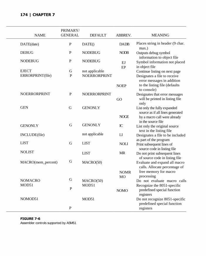
174 | CHAPTER 7
NAMEPRIMARY/GENERAL DEFAULT ABBREV. MEANING
DATE(date)
DEBUG
NODEBUG
EJECTERRORPRINT(file)
NOERRORPRINT
GEN
GENONLY
INCLUDE(file)
LIST
NOLIST
MACRO(mem_percent)
NOMACROMOD51
NOMOD51
P
P
P
GP
P
G
G
G
G
G
P
P
DATE()
NODEBUG
NODEBUG
not applicableNOERRORPRINT
NOERRORPRINT
GENONLY
GENONLY
not applicable
LIST
LIST
MACRO(50)
MACRO(50)MOD51
MOD51
DADB
NODB
EJEP
NOEP
GO
NOGE
IC
LI
NOLI
MR
NOMRMO
NOMO
Places string in header (9 char.max.)
Outputs debug symbolinformation to object file
Symbol information not placedin object fileContinue listing on next pageDesignates a file to receive
error messages in additionto the listing file (defaultsto console)
Designates that error messageswill be printed in listing fileonly
List only the fully expandedsource as if all lines generatedby a macro call were alreadyin the source file
List only the original sourcetext in the listing file
Designates a file to be includedas part of the programPrint subsequent lines of
source code in listing fileDo not print subsequent lines
of source code in listing fileEvaluate and expand all macro
calls. Allocate percentage offree memory for macroprocessing
Do not evaluate macro callsRecognize the 8051-specific
predefined special functionregisters
Do not recognize 8051-specificpredefined special functionregisters
FIGURE 7-6
Assembler controls supported by ASM51

NAMEPRIMARY/GENERAL DEFAULT ABBREV. MEANING
OBJECT(file) P OBJECT(source.OBJ) OJ Designates file to receiveobject code
NOOBJECT P OBJECT(source.OBJ) NOOJ Designates that no objectfile will be created
PAGING P PAGING PI Designates that listing filebe broken into pages andeach will have a header
NOPAGING P PAGING NOPI Designates that listing file willcontain no page breaks
PAGELENGTH(N) P PAGELENGT(60) PL Sets maximum number of linesin each page of listing file(range = 10 to 65,536)
PAGE WIDTH(N) P PAGEWIDTH(120) PW Sets maximum number ofcharacters in each line oflisting file (range = 72 to 132)
PRINT(file) P PRINT(source.LST) PR Designates file to receivesource listing
NOPRINT P PRINT(source.LST) NOPR Designates that no listingfile will be created
SAVE G not applicable SA Stores current control settingsfrom SAVE stack
RESTORE G not applicable RS Restores control settings fromSAVE stack
REGISTERBANK(rb,...) P REGISTERBANK(0) RB Indicates one or more banksused in program module
NOREGISTERBANK P REGISTERBANK(0) NORB Indicates that no register banksare used
SYMBOLS P SYMBOLS SB Creates a formatted table of allsymbols used in program
NOSYMBOLS P SYMBOLS NOSB Designates that no symboltable is created
TITLE(string) G TITLE() TT Places a string inallCTubsequent pageheaders (max. 60 characters)
WORKFILES(path) P same as source WF Designates alternate pathfor temporary workfiles
XREF P NOXREF XR Creates a cross referencelisting of all symbolsused in program
NOXREF P NOXREF NOXR Designates that no crossreference list is created
FIGURE 7-6continued
175
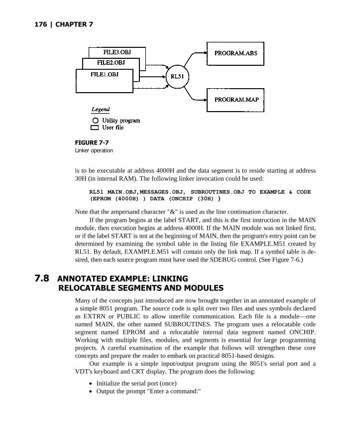
176 | CHAPTER 7
FIGURE 7-7
Linker operation
is to be executable at address 4000H and the data segment is to reside starting at address30H (in internal RAM). The following linker invocation could be used:
RL51 MAIN.OBJ,MESSAGES.OBJ, SUBROUTINES.OBJ TO EXAMPLE & CODE(EPROM (4000H) ) DATA (ONCHIP (30H) )
Note that the ampersand character "&" is used as the line continuation character.
If the program begins at the label START, and this is the first instruction in the MAINmodule, then execution begins at address 4000H. If the MAIN module was not linked first,or if the label START is not at the beginning of MAIN, then the program's entry point can bedetermined by examining the symbol table in the listing file EXAMPLE.M51 created byRL51. By default, EXAMPLE.M51 will contain only the link map. If a symbol table is de-sired, then each source program must have used the SDEBUG control. (See Figure 7-6.)
7.8 ANNOTATED EXAMPLE: LINKINGRELOCATABLE SEGMENTS AND MODULES
Many of the concepts just introduced are now brought together in an annotated example ofa simple 8051 program. The source code is split over two files and uses symbols declaredas EXTRN or PUBLIC to allow interfile communication. Each file is a module—onenamed MAIN, the other named SUBROUTINES. The program uses a relocatable codesegment named EPROM and a relocatable internal data segment named ONCHIP.Working with multiple files, modules, and segments is essential for large programmingprojects. A careful examination of the example that follows will strengthen these coreconcepts and prepare the reader to embark on practical 8051-based designs.
Our example is a simple input/output program using the 8051's serial port and aVDT's keyboard and CRT display. The program does the following:
Initialize the serial port (once) Output the prompt "Enter a command:"

ASSEMBLY LANGUAGE PROGRAMMING | 177
Input a line from the keyboard, echoing each character as it is received Echo back the entire line Repeat
Figure 7-8 shows (a) the listing file (ECHO.LST) for the first source file, (b) the list-ing file (IO.LST) for the second source file, and (c) the listing file (EXAMPLE.M51) cre-ated by the linker/locator.
7.8.1 ECHO.LST
Figure 7-8a shows the contents of the file ECHO.LST created by ASM51 when the sourcefile (ECHO.SRC) was assembled. The first several lines in the listing file provide generalinformation on the programming environment. Among other things, the invocation line isrestated in an expanded form showing the path to the files. Note the use of the assemblercontrol EP (for ERRORPRINT) on the invocation line. This causes error messages to besent to the console as well as the listing file. (See Figure 7-6.)
The original source file is shown under the column heading SOURCE, just to theright of the column LINE. As evident, ECHO.SRC contains 22 lines. Lines 1 to 4 containassembler controls. (See Figure 7-6.) $DEBUG inline 1 instructs ASM51 to place a sym-bol table in the object file, ECHO.OBJ. This is necessary for hardware emulation or forthe linker/locator to create a symbol table in its listing file. $TITLE defines a string to beplaced at the top of each page of the listing file. $PAGEW1DTH specifies the maximumwidth of each line in the listing file. $NOPAGING prevents page breaks (form feeds) frombeing inserted into the listing file. Most assembler controls affect the look of the outputlisting file. Some trial and error will usually produce the desire output for printing.
The NAME assembler directive in line 6 defines the current file as part of the mod-ule MAIN. For this example, no further instance of the MAIN module is used; however,larger projects may include other files also defined as part of the MAIN module. It mayhelp the reader for the rest of this example to read "file" for the term "module."
Lines 7 and 8 identify the symbols used in the current module but defined elsewhere.Without these EXTRN directives, ASM51 will generate the message "undefined symbol"on each line in the source program where one of these symbols is used. The "segmenttype" must also be defined for each symbol to ensure its proper use. All of the externalsymbols defined in this example are of type CODE.
Symbol definitions come next. Line 10 defines the symbol CR as the carriage returnASCII code 0DH. Line 11 defines the symbol EPROM as a segment of type CODE. Recallthat the SEGMENT directive defines only what the symbol is—nothing more, nothing less.
The RSEG directive in line 13 begins the relocatable segment named EPROM. SubFrequent instructions, data constant definitions, and so on, will be placed in the EPROMcode segment.
The program begins on line 14 at the label MAIN. The first instruction in the programis a call to the subroutine INIT, which will initialize the 8051's serial port. The assembledcode under the OBJ column contains the correct opcode (12H for LCALL); however, bytes2 and 3 of the instruction (the address of the subroutine) appear as 0000H followed by theletter "F." The linker/locator must "fix" this when the program modules are linked together

FIGURE 7-8a
Annotated example: linking relocatable segments and modules. (a) ECHO.LST. (b) IO.LST. (c) EXAMPLE.M51.
178
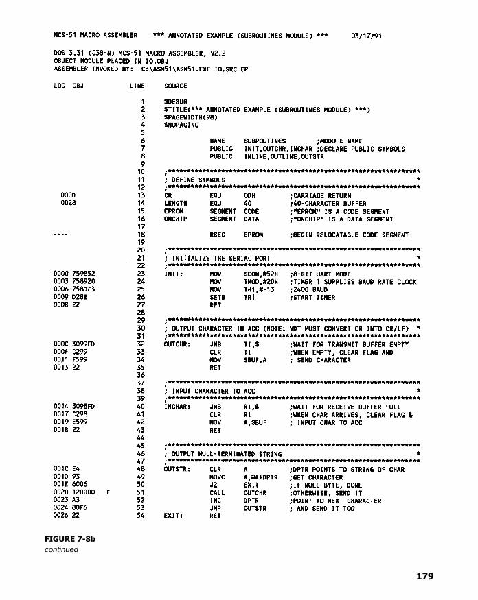
FIGURE 7-8b
continued
179
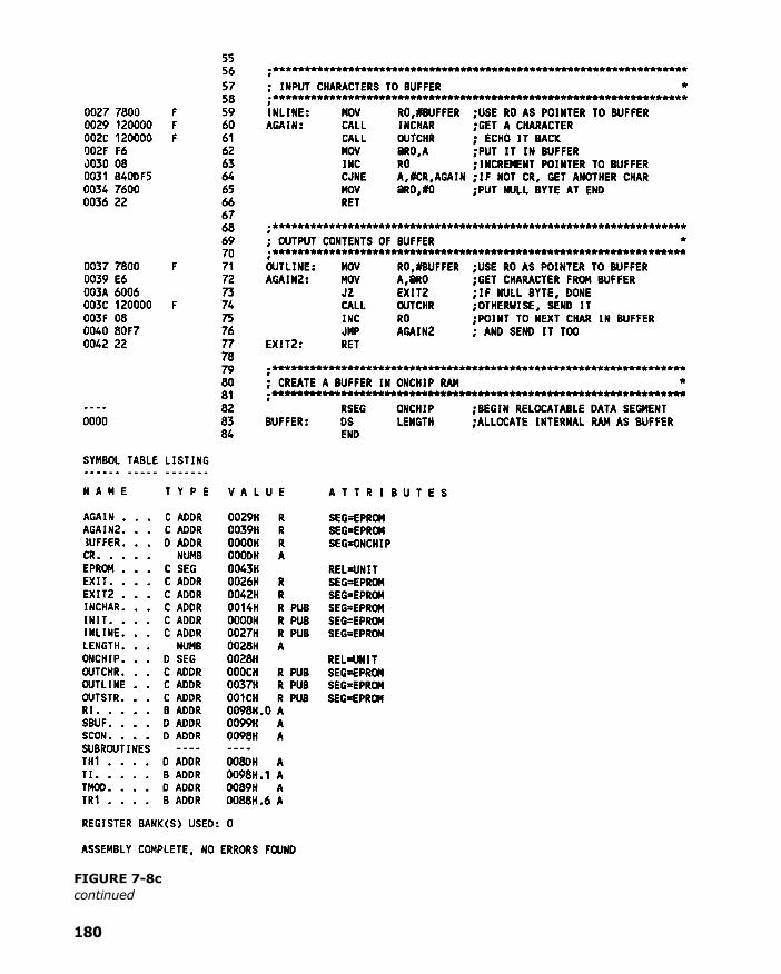
FIGURE 7-8c
continued
180

FIGURE 7-8d
continued
181

182 | CHAPTER 7
and addresses are set for the relocatable segments. Note, too, that the address under theLOC column is also entered as 0000H. Since the EPROM segment is relocatable, it is notknown at assemble-time where the segment will start. All relocatable segments willdisplay 0000H as the starting address in the listing file.
The rest of the program instructions are on lines 15 to 19. A prompt message is sentto the VDT by loading the DPTR with a starting address of the prompt and calling the sub-routine OUTSTR. Since the OUTSTR, INLINE, and OUTLINE subroutines are not de-fined in ECHO.SRC, one can only guess at their operation from the name of thesubroutine and the comment lines.
The prompt is a null-terminated ASCII string, which is placed in the EPROM codesegment using the DB (define byte) directive on line 21. Since the prompt bytes are con-stant (i.e., unchanging), it is correct to place them in code memory (even though they aredata bytes). The prompt begins with a carriage return to ensure it displays on a new line.(In this example, it is assumed the VDT converts CR to CR/LF.)
All the symbols and labels in ECHO.SRC appear in the symbol table at the bottom ofECHO.LST. Since the EPROM segment is relocatable and the subroutines are external,the VALUE column is not of much use. The value for the symbol EPROM, however,gives the length of the segment, which in this case is 24H or 36 bytes.
7.8.2 IO.LST
Figure 7-8b shows the contents of the file IO.LST—the file containing the input/outputsubroutines. This module is named SUBROUTINES in line 6. Lines 7 and 8 declare allsubroutine names as PUBLIC symbols. This makes these symbols available to othermodules. Note that all the subroutines are made public even though only four of themwere used in the MAIN module. Perhaps, as the program grows, other modules will beadded that may need these subroutines. So, they are all made public.
Lines 13 to 16 define several symbols. Once again, EPROM is used as the name ofthe code segment. Another segment is used in this module. ONCHIP is defined in line 17as an internal data segment.
The subroutines are each written in turn beginning at line 20. The comment block be-ginning each is deliberately brief in this example; however, a more detailed description ofa subroutine is usually given. It is useful to provide, for example, entry and exit conditionsfor each subroutine.
After the last subroutine, a buffer in internal RAM is created using the ONCHIP seg-ment. The segment is started using RSEG (line 82), and the buffer is created using the DS(define storage) directive (line 83). The length of the buffer is assigned to the symbolLENGTH "equated" at the top of the program (line 14) as 40. The placement in the sourcefile of the definition of the symbol LENGTH and of the instance of the segment ONCHIPis largely a matter of taste. Both could also be positioned just before or after the INLINEsubroutine, where they are used.
As with the EPROM segment, ONCHIP is given an initial address of 0000H under theLOC column at line 83. Again, the actual location of the ONCHIP segment will not bedetermined until link-time (see below). The letter "F' appears in numerous locations inIO.LST. Each line so identified contains an instruction using a symbol whose value cannot
ASSEMBLY LANGUAGE PROGRAMMING | 183
be determined at assemble-time. The zeros placed in the object file at these locations willbe replaced with "absolute" values by the linker/locator.
7.8.3 EXAMPLE.M51
Figure 7-8c shows the contents of the file EXAMPLE.M51 created by the linker/locatorprogram, RL51. The invocation line is repeated near the top of EXAMPLE.M51 andshould be examined carefully. Here it is again (leaving out the path):
RL51 ECHO.OBJ,IO.OBJ TO EXAMPLE CODE (EPROM (8000H)) & DATA(ONCHIP (30H))
Following the command, the object modules are listed separated by commas in the orderthey are to be linked. Following the input list, the optional control TO EXAMPLE is spec-ified providing the name for the absolute object module created by RL51. If omitted, thename of the first file in the input list is used (without any file extension). The listing file,in this example, automatically takes on the name EXAMPLE.M51. Finally, the locatingcontrols CODE and DATA specify the names of segments of the associated type and theabsolute address at which the segment is to begin. In this example the EPROM codesegment begins at address 8000H and the ONCHIP data segment begins at byte address30H in the 8051's internal RAM.
Following the restatement of the invocation line, EXAMPLE.M151 contains a list ofthe input modules included by RL51. In this example only two files (ECHO.OBJ andIO.OBJ) and two modules (MAIN and SUBROUTINES) are listed. If the NAME directivehad not been used in the source files, the module names would be the same as the file names.
The link map appears next. Both the ONCHIP and EPROM segments are identified,and the starting address and the length (in hexadecimal) are given for each. ONCHIP isidentified as a data segment starting at address 30H and 28H (40) bytes in length. EPROMis identified as a code segment starting at address 8000H and 67H (103) bytes in length.
Finally, EXAMPLE.M51 contains a symbol table. All symbols (including labels) usedin the program are listed, sorted on a module-by-module basis. All values are "absolute."Remember that the symbol table in the .M51 file can only be created if the $DEBUGassembler control is placed at the top of each source file. The INIT subroutine address(which we noted earlier was absent in ECHO.LST) is identified under the SUBROUTINESmodule as 8024H. This address is substituted as the code address in any object module usingthe instruction CALL INIT, as noted earlier in the MAIN module. Knowing the absolutevalue of labels is important when debugging. When a bug is found, often a temporary"patch" can be made by modifying the program bytes and re-executing the program. If thepatch fixes the bug, the appropriate change is made to the source program.
7.9 MACROS
For the final topic in this chapter, we return to ASM51. The macro processing facility(MPL) of ASM51 is a "string replacement" facility. Macros allow frequently used sectionsof code to be defined once using a simple mnemonic and used anywhere in the program by
184 | CHAPTER 7
inserting the mnemonic. Programming using macros is a powerful extension of the tech-niques described thus far. Macros can be defined anywhere in a source program and sub-sequently used like any other instruction. The syntax for a macro definition is
%*DEFINE (call_pattern) (macro_body)
Once defined, the call pattern is like a mnemonic; it may be used like any assemblylanguage instruction by placing it in the mnemonic field of a program. Macros are madedistinct from "real" instructions by preceding them with a percent sign, "%". When thesource program is assembled, everything within the macro-body, on a character-by-character basis, is substituted for the call-pattern. The mystique of macros is largely un-founded. They provide a simple means for replacing cumbersome instruction patterns withprimitive, easy-to-remember mnemonics. The substitution, we reiterate, is on a character-by-character basis-nothing more, nothing less.
For example, if the following macro definition appears at the beginning of a source file,
%*DEFINE (PUSH_DPTR)(PUSH DPHPUSH DPL)
then the statement
%PUSHDPTR
will appear in the .LST file as
PUSH DPHPUSH DPL
The example above is a typical macro. Since the 8051 stack instructions operateonly on direct addresses, pushing the data pointer requires two PUSH instructions. Asimilar macro can be created to POP the data pointer.
There are several distinct advantages in using macros:
A source program using macros is more readable, since the macro mnemonic isgenerally more indicative of the intended operation than the equivalent assemblerinstructions.
The source program is shorter and requires less typing. Using macros reduces bugs. Using macros frees the programmer from dealing with low-level details.
The last two points above are related. Once a macro is written and debugged, it is used freelywithout the worry of bugs. In the PUSH_DPTR example above, if PUSH and POP instruc-tions are used rather than push and pop macros, the programmer may inadvertently reversethe order of the pushes or pops. (Was it the high-byte or low-byte that was pushed first?) Thiswould create a bug. Using macros, however, the details are worked out once—when themacro is written—and the macro is used freely thereafter, without the worry of bugs.
Since the replacement is on a character-by-character basis, the macro definitionshould be carefully constructed with carriage returns, tabs, etc., to ensure proper alignment
ASSEMBLY LANGUAGE PROGRAMMING | 185
of the macro statements with the rest of the assembly language program. Some trial anderror is required.
There are advanced features of ASM51's macro-processing facility that allow forparameter passing, local labels, repeat operations, assembly flow control, and so on. Theseare discussed below.
7.9.1 Parameter Passing
A macro with parameters passed from the main program has the following modified
format:
%*DEFINE (macro_name (parameter_list)) (macro_body)
For example, if the following macro is defined,
%*DEFINE (CMPA# (VALUE))(CINE A,#%VALUE,$ + 3)
then the macro call
%CPA# (20H)
will expand to the following instruction in the .LST file:
CJNE A,#20H,$ + 3
Although the 8051 does not have a "compare accumulator" instruction, one is easily cre-ated using the CJNE instruction with "$ +3" (the next instruction) as the destination for theconditional jump. The CMPA# mnemonic may be easier to remember for many program-mers. Besides, use of the macro unburdens the programmer from remembering notationaldetails, such as " $ +3."
Let's develop another example. It would be nice if the 8051 had instructions such as
JUMP IF ACCUMULATOR GREATER THAN XJUMP IF ACCUMULATOR GREATER THAN OR EQUAL TO XJUMP IF ACCUMULATOR LESS THAN X
JUMP IF ACCUMULATOR LESS THAN OR EQUAL TO X
but it does not. These operations can be created using CJNE followed by JC or JNC, but thedetails are tricky. Suppose, for example, it is desired to jump to the label GREATER_THANif the accumulator contains an ASCII code greater than "Z" (5AH). The following instructionsequence would work:
CJNE A,#5BH,$+3JNC GREATER_THAN
The CJNE instruction subtracts 5BH (i.e., "Z" + 1) from the content of A and sets or clearsthe carry flag accordingly. CJNE leaves C = 1 for accumulator values 00H up to andincluding 5AH. (Note: 5AH - 5BH < 0, therefore C = 1; but 5BH - 5BH = 0,

186 | CHAPTER 7
therefore C = 0.) Jumping to GREATER_THAN on the condition "not carry" correctlyjumps for accumulator values 5BH, 5CH, 5DH, and so on, up to FFH. Once details suchas these are worked out, they can be simplified by inventing an appropriate mnemonic,defining a macro, and using the macro instead of the corresponding instruction sequence.Here's the definition for a "jumps if greater than" macro:
%*DEFINE (JGT(VALUE, LABEL))(CJNE A,#%VALUE+1,$+3 ;JGTJNC %LABEL)
To test if the accumulator contains an ASCII code greater than "Z," as just discussed, themacro would be called as
%JGT ('Z',GREATER_THAN)
ASM5 1 would expand this into
CJNE A,#5BH,$+3 ;JGTJNC GREATER_THAN
The JGT macro is an excellent example of a relevant and powerful use of macros. By us-ing macros, the programmer benefits by using a meaningful mnemonic and avoidingmessy and potentially bug-ridden details.
7.9.2 Local Labels
Local labels may be used within a macro using the following format:
%*DEFINE(macro_name [(parameter_list)])[LOCAL list_of_local_labels] (macro_body)
For example, the following macro definition
%*DEFINE (DEC_DPTR) LOCAL SKIP(DEC DPL ;DECREMENT DATA POINTERMOV A,DPL
CJNE A,#0FFH,%SKIPDEC DPH
%SKIP:
would be called as
%DECDPTR
and would be expanded by ASM51 into
DEC DPL ;DECREMENT DATA POINTERMOV A,DPLCJNE A, #0FFH, SKIP00DEC DPH
SKIP00
ASSEMBLY LANGUAGE PROGRAMMING | 187
Note that a local label generally will not conflict with the same label used elsewhere in thesource program, since ASM51 appends a numeric code to the local label when the macrois expanded. Furthermore, the next use of the same local label receives the next numericcode, and so on.
The macro above has a potential "side effect." The accumulator is used as a tempo-rary holding place for DPL. If the macro is used within a section of code that uses A foranother purpose, the value in A would be lost. This side effect probably represents a bugin the program. The macro definition could guard against this by saving A on the stack.Here's an alternate definition for the DEC_DPTR macro:
%*DEFINE (DEC_DPTR) LOCAL SKIP(PUSHACC
DEC DPL ;DECREMENT DATA POINTERMOV A,DPL
CJNE A,#0FFH,%SKIPDEC DPH
%SKIP: POP ACC
)
7.9.3 Repeat Operations
This is one of several built-in (predefined) macros. The format is
%REPEAT (expression) (text)
For example, to fill a block of memory with 100 NOP instructions,
%REPEAT(100) (NOP
)
7.9.4 Control Flow Operations
The conditional assembly of sections of code is provided by ASM51's control flow macrodefinition. The format is
%IF(expression) THEN (balanced_text)[ELSE (balanced_text) ]FI
For example,
INTERNAL EQU 1 ;1 = 8051 SERIAL I/O DRIVERS;0 = 8251 SERIAL I/O DRIVERS
.
.%IF (INTERNAL) THEN
(INCHED: . ;8051 DRIVERS
OUTCHR:
188 | CHAPTER 7
)ELSE(INCHED: ;8251 DRIVERS
OUTCHR:
In this example, the symbol INTERNAL is given the value 1 to select I/O subroutinesfor the 8051's serial port, or the value 0 to select I/O subroutines for an external UART,in this case the 8251. The IF macro causes ASM51 to assemble one set of drivers andskip over the other. Elsewhere in the program, the INCHAR and BUTCHERsubroutines are used without consideration for the particular hardware configuration.As long as the program as assembled with the correct value for INTERNAL, the correctsubroutine is executed.
SUMMARY
This chapter has presented major concepts of assembly language programming the 8051,including standard program formats and the use of assembler directives and macros to helpmake a program more readable, compact, and orderly.
As program sizes increase, one wonders if there are other ways to write 8051 pro-grams in a more structured and English-like manner. In the next chapter, we will discusssuch an alternative, the 8051 C language.
PROBLEMS
7.1 Recast the following instructions with the operand expressed in binary.
MOV A,#255
MOV A,#11Q
MOV A,#11Q
MOV A,#'A'
7.2 Recast each of the following instructions with the operand expressed in hexadecimal.
MOV A,#255
MOV A,#-3
MOV A,#'z'
MOV A,#'33Q
MOV A,#'$'
MOV A,#64
7.3 What is wrong with the coding of the following instruction?
ORL 80H,#F0H

ASSEMBLY LANGUAGE PROGRAMMING | 189
7.4 Identify the error in the following symbols.
?byte.bit
@GOOD_bye
1ST_FLAG
MY_PROGRAM
7.5 Recast the following instructions with the expression evaluated as a 16-bit hexa-decimal constant.
MOV DPTR, # 'C' EQ 48
MOV DPTR,# HIGH'AB'
MOV DPTR,#-1
MOV DPTR,#NOT (257 MOD 256)
7.6 Recast each of the following instructions with the source location specified as ahexadecimal address, rather than in symbolic form.
MOV A, PSW
MOV A, P0
MOV A, DPH
MOV A, TLC
MOV A, IP
MOV A, TMOD
7.7 Recast each of the following instructions with the source location specified in sym-bolic form, rather than as a hexadecimal address.
MOV A,0B0H
MOV A,99H
MOV A,82H
MOV A,85H
MOV A,0A8H
MOV A,0D0H
7.8 What are the "segment types" defined by ASM51 for the 8051, and what memoryspaces do they represent?
7.9 How could a relocatable segment in external data memory be defined, selected, anda 100-byte buffer created? (Give the segment the name "OFFCHIP" and give thebuffer the name "BUFFER.")
7.10 A certain application requires five status bits (FLAG1 to FLAGS). How could a 5-bit buffer be defined in an absolute BIT segment starting at bit address 0811? Atwhat byte address do these bits reside?
7.11 What are two good reasons for making generous use of the EQU directive inassembly language programs?
7.12 What is the difference between the DB and DW directives?7.13 What are the memory assignments for the following assembler directives:
ORG 0FH
DW $ SHL4 4
D5 65535
DW 'C'

190 | CHAPTER 7
7.14 What directive is used to select an absolute code segment?7.15 A file called "ASCII" contains 33 equate directives, one for each control code:
NUL EQU 0CH ;NULL 5YTE
SOH EQU 01H ;STEDT OF HEADER
US EQU 7FH ;UNIT SEPARATOR
DEL EQU 7FH ;DELETE
How could these definitions be made known in another file—a source program—without actually inserting the equates into that file?
7.16 In order for a printout of a listing file to look nice, it is desirable to have eachsub-routine begin at the top of a page. How is this accomplished?
7.17 Write the definition for a macro that could be used to fill a block of external datamemory with a data constant. Pass the starting address, length, and data constant tothe macro as parameters.
7.18 Write the definition for the following macros:
JGE-jump to LABEL if accumulator is greater than or equal to VALUEJLT-jump to LABEL if accumulator is less than VALUEJGE-jump to LABEL if accumulator is less than or equal to VALUEJGE-jump to LABEL if accumulator is outside the range LOWER and UPPER
7.19 Write the definition for a macro called CJNE DPTR that will jump to LABEL ifthe data pointer does not contain VALUE. Define the macro so that the contents ofall registers and memory locations are left intact.

8051 C Programming
8.1 INTRODUCTION
Throughout the earlier chapters, we have discussed how to communicate with the 8051 byusing the assembly language. In fact, there is another way by which we can talk to the 8051.This is called 8051 C language, an often-preferred choice when the complexity of a programincreases considerably. This chapter introduces the 8051 C language as an alternative to theassembly language programming. The choice of which to use is entirely up to you, theprogrammer. Factors that commonly influence such a decision are the desired speed, codesize, and ease of programming. Since the intent of this chapter is to present the basics ofprogramming the 8051 in C, we will assume that the reader is already familiar with con-ventional C programming, as is often the case due to C's popularity and widespread usage.
8.2 ADVANTAGES AND DISADVANTAGES OF 8051 C
The advantages of programming the 8051 in C as compared to assembly are:
Offers all the benefits of high-level, structured programming languages such as C,including the ease of writing subroutines, and others discussed in more detail inSection 9.2
Often relieves the programmer of the hardware details that the compiler handleson behalf of the programmer
Easier to write, especially for large and complex programs Produces more readable program source codes
Nevertheless, 8051 C, being very similar to the conventional C language, also suffersfrom the following disadvantages:
191

192 | CHAPTER 8
Possesses the disadvantages of high-level, structured programming languages, as
mentioned in Section 9.2 Generally generates larger machine codes Programmer has less control and less ability to directly interact with the hardware
To compare between 8051 C and assembly language, consider the solution to Example4.5, written below in 8051 C language.
sbit portbit = P1^0; /* Use variable portbit to refer to P1.0 */main( )TMOD = 1;{while (1)
{TH0 = 0xFE;TL0 = 0xC;TR0 = 1;while (TF0 != 1);TR0 = 0;TF0 = 0;portbit = !(P1^0);}
}
Notice that both the assembly and C language solutions for Example 4.5 require almost thesame number of lines. However, the difference lies in the readability of these programs. TheC version seems more human than assembly, and is hence more readable. This often helpsfacilitate the human programmer's efforts to write even very complex programs. The assem-bly language version is more closely related to the machine code, and though less readable,often results in more compact machine code. As with this example, the resultant machinecode from the assembly version takes 83 bytes while that of the C version requires 149bytes, an increase of 79.5%!
The human programmer's choice of either high-level C language or assembly lan-guage for talking to the 8051, whose language is machine language, presents aninteresting picture, as shown in Figure 8-1.
8.3 8051 C COMPILERS
We saw in Figure 8-1 that a compiler is needed to convert programs written in 8051 C languageinto machine language, just as an assembler is needed in the case of programs written inassembly language. A compiler basically acts just like an assembler, except that it is more com-plex since the difference between C and machine language is far greater than that between as-sembly and machine language. Hence the compiler faces a greater task to bridge that difference.
Currently, there exist various 8051 C compilers, which offer almost similar functions.All our examples and programs have been compiled and tested with Keil's µVision 2 IDE

8051 C PROGRAMMING | 193
FIGURE 8-1
Conversion between human, high-level, assembly, and machine language
by Keil Software,1 an integrated 8051 program development environment that includes itsC51 cross compiler for C (Refer to Appendix H for a guide to using µVision 2 IDE). Across compiler is a compiler that normally runs on a platform such as IBM compatible PCsbut is meant to compile programs into codes to be run on other platforms such as the 8051.
8.4 DATA TYPES
8051 C is very much like the conventional C language, except that several extensions andadaptations have been made to make it suitable for the 8051 programming environment.The first concern for the 8051 C programmer is the data types. Recall that a data type issomething we use to store data. Readers will be familiar with the basic C data types suchas int, char, and float, which are used to create variables to store integers, characters, orfloating-points. In 8051 C, all the basic C data types are supported, plus a few additionaldata types meant to be used specifically with the 8051.
Table 8-1 gives a list of the common data types used in 8051 C. The ones in bold arethe specific 8051 extensions. The data type bit can be used to declare variables that residein the 8051's bit-addressable locations (namely byte locations 20H to 2FH or bit locations00H to 7FH). Obviously, these bit variables can only store bit values of either 0 or 1. Asan example, the following C statement:
bit flag = 0;
declares a bit variable called flag and initializes it to 0.The data type sbit is somewhat similar to the bit data type, except that it is normally
used to declare 1-bit variables that reside in special function registers (SFRs). For example:
sbit P = 0xD0;
1Keil Software, Inc., 1501 10a' Street, Suite 110, Plano, TX 75074. Website: http://www.keil.com
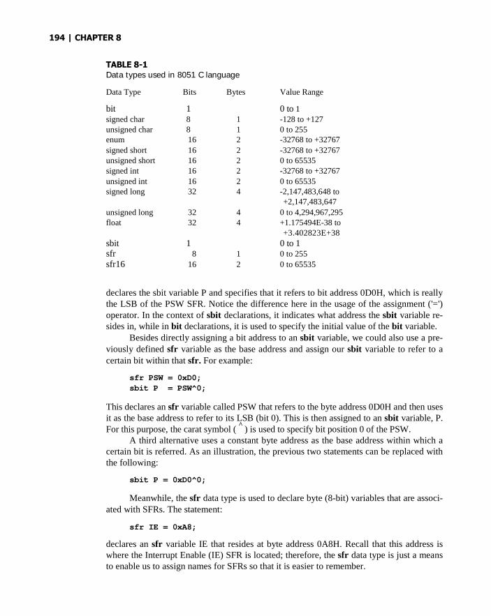
194 | CHAPTER 8
TABLE 8-1Data types used in 8051 C language
Data Type Bits Bytes Value Range
bit 1 0 to 1signed char 8 1 -128 to +127unsigned char 8 1 0 to 255enum 16 2 -32768 to +32767
signed short 16 2 -32768 to +32767unsigned short 16 2 0 to 65535signed int 16 2 -32768 to +32767
unsigned int 16 2 0 to 65535signed long 32 4 -2,147,483,648 to
+2,147,483,647
unsigned long 32 4 0 to 4,294,967,295float 32 4 +1.175494E-38 to
+3.402823E+38
sbit 1 0 to 1sfr 8 1 0 to 255
sfr16 16 2 0 to 65535
declares the sbit variable P and specifies that it refers to bit address 0D0H, which is reallythe LSB of the PSW SFR. Notice the difference here in the usage of the assignment ('=')operator. In the context of sbit declarations, it indicates what address the sbit variable re-sides in, while in bit declarations, it is used to specify the initial value of the bit variable.
Besides directly assigning a bit address to an sbit variable, we could also use a pre-viously defined sfr variable as the base address and assign our sbit variable to refer to acertain bit within that sfr. For example:
sfr PSW = 0xD0;sbit P = PSW^0;
This declares an sfr variable called PSW that refers to the byte address 0D0H and then usesit as the base address to refer to its LSB (bit 0). This is then assigned to an sbit variable, P.For this purpose, the carat symbol (
^) is used to specify bit position 0 of the PSW.
A third alternative uses a constant byte address as the base address within which acertain bit is referred. As an illustration, the previous two statements can be replaced withthe following:
sbit P = 0xD0^0;
Meanwhile, the sfr data type is used to declare byte (8-bit) variables that are associ-ated with SFRs. The statement:
sfr IE = 0xA8;
declares an sfr variable IE that resides at byte address 0A8H. Recall that this address iswhere the Interrupt Enable (IE) SFR is located; therefore, the sfr data type is just a meansto enable us to assign names for SFRs so that it is easier to remember.
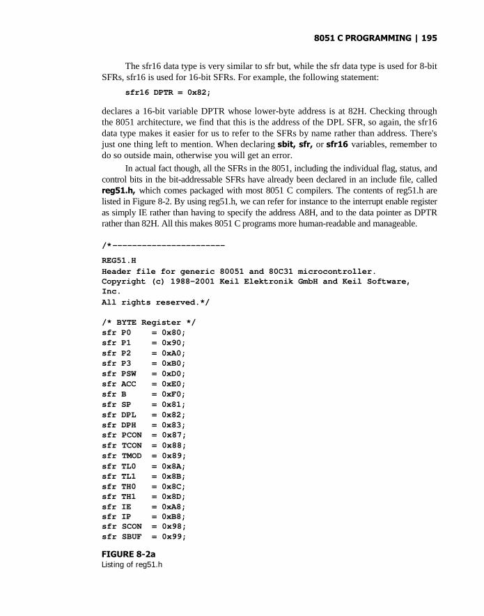
8051 C PROGRAMMING | 195
The sfr16 data type is very similar to sfr but, while the sfr data type is used for 8-bitSFRs, sfr16 is used for 16-bit SFRs. For example, the following statement:
sfr16 DPTR = 0x82;
declares a 16-bit variable DPTR whose lower-byte address is at 82H. Checking throughthe 8051 architecture, we find that this is the address of the DPL SFR, so again, the sfr16data type makes it easier for us to refer to the SFRs by name rather than address. There'sjust one thing left to mention. When declaring sbit, sfr, or sfr16 variables, remember todo so outside main, otherwise you will get an error.
In actual fact though, all the SFRs in the 8051, including the individual flag, status, andcontrol bits in the bit-addressable SFRs have already been declared in an include file, calledreg51.h, which comes packaged with most 8051 C compilers. The contents of reg51.h arelisted in Figure 8-2. By using reg51.h, we can refer for instance to the interrupt enable registeras simply IE rather than having to specify the address A8H, and to the data pointer as DPTRrather than 82H. All this makes 8051 C programs more human-readable and manageable.
/*-----------------------
REG51.H
Header file for generic 80051 and 80C31 microcontroller.Copyright (c) 1988-2001 Keil Elektronik GmbH and Keil Software,Inc.
All rights reserved.*/
/* BYTE Register */sfr P0 = 0x80;sfr P1 = 0x90;
sfr P2 = 0xA0;sfr P3 = 0xB0;sfr PSW = 0xD0;sfr ACC = 0xE0;sfr B = 0xF0;sfr SP = 0x81;sfr DPL = 0x82;sfr DPH = 0x83;sfr PCON = 0x87;
sfr TCON = 0x88;sfr TMOD = 0x89;
sfr TL0 = 0x8A;sfr TL1 = 0x8B;sfr TH0 = 0x8C;sfr TH1 = 0x8D;sfr IE = 0xA8;sfr IP = 0xB8;sfr SCON = 0x98;sfr SBUF = 0x99;
FIGURE 8-2aListing of reg51.h

/* BIT Register
*/ /* PSW */
sbit CY = 0xD7;sbit AC = 0xD6;
sbit F0 = 0xD5;sbit RS1 = 0xD4;sbit RS0 = 0xD3;
sbit OV = 0xD2;
sbit P = OxDO;
/* TCON */
sbit TF1 = 0x8F;
sbit TR1 = 0x8E;
sbit TF0 = 0x8D;
sbit TR0 = 0x8C;
sbit IE1 = 0x8B;
sbit IT1 = 0x8A;
sbit IE0 = 0x89;
sbit IT0 = 0x88;
/* IE */
sbit EA = 0xAF;sbit ES = 0xAC;
sbit ET1 = 0xAB;
sbit EX1 = 0xAA;
sbit ET0 = 0xA9;
sbit EX0 = 0xA8;
/* IP */sbit PS = 0xBC;
sbit PT1 = 0xBB;
sbit PX1 = 0xBA;
sbit PT0 = 0xB9;
sbit PX0 = 0xB8;
/* P3 */
sbit RD = 0xB7;
sbit WR = 0xB6;
sbit T1 = 0xB5;sbit T0 = 0xB4;sbit INT1 = 0xB3;sbit INT0 = 0xB2;sbit TXD = 0xBl;sbit RXD = 0xB0;
/* SCON */sbit SM0 = 0x9F;sbit SM1 = 0x9E;sbit SM2 = 0x9D;sbit REN = 0x9C;sbit TB8 = 0x9B;sbit RB8 = 0x9A;
sbit TI = 0x99;
sbit RI = 0x98;
FIGURE 8-2b
continued196
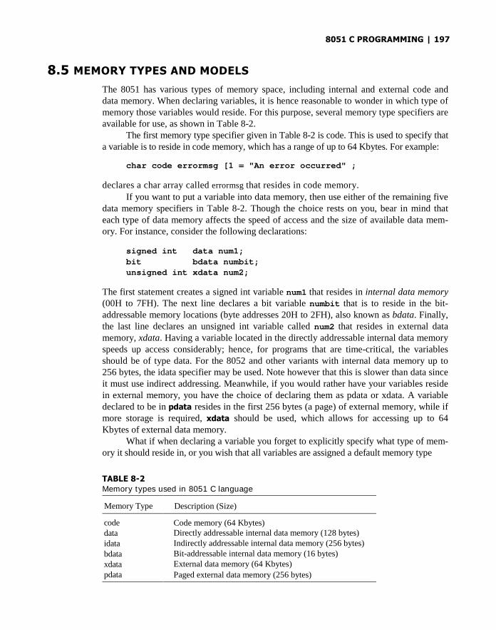
8051 C PROGRAMMING | 197
8.5 MEMORY TYPES AND MODELS
The 8051 has various types of memory space, including internal and external code anddata memory. When declaring variables, it is hence reasonable to wonder in which type ofmemory those variables would reside. For this purpose, several memory type specifiers areavailable for use, as shown in Table 8-2.
The first memory type specifier given in Table 8-2 is code. This is used to specify thata variable is to reside in code memory, which has a range of up to 64 Kbytes. For example:
char code errormsg [1 = "An error occurred" ;
declares a char array called errormsg that resides in code memory.
If you want to put a variable into data memory, then use either of the remaining fivedata memory specifiers in Table 8-2. Though the choice rests on you, bear in mind thateach type of data memory affects the speed of access and the size of available data mem-ory. For instance, consider the following declarations:
signed int data num1;
bit bdata numbit;unsigned int xdata num2;
The first statement creates a signed int variable num1 that resides in internal data memory(00H to 7FH). The next line declares a bit variable numbit that is to reside in the bit-addressable memory locations (byte addresses 20H to 2FH), also known as bdata. Finally,the last line declares an unsigned int variable called num2 that resides in external datamemory, xdata. Having a variable located in the directly addressable internal data memoryspeeds up access considerably; hence, for programs that are time-critical, the variablesshould be of type data. For the 8052 and other variants with internal data memory up to256 bytes, the idata specifier may be used. Note however that this is slower than data sinceit must use indirect addressing. Meanwhile, if you would rather have your variables residein external memory, you have the choice of declaring them as pdata or xdata. A variabledeclared to be in pdata resides in the first 256 bytes (a page) of external memory, while ifmore storage is required, xdata should be used, which allows for accessing up to 64Kbytes of external data memory.
What if when declaring a variable you forget to explicitly specify what type of mem-ory it should reside in, or you wish that all variables are assigned a default memory type
TABLE 8-2
Memory types used in 8051 C language
Memory Type Description (Size)
codedataidatabdataxdatapdata
Code memory (64 Kbytes)Directly addressable internal data memory (128 bytes)Indirectly addressable internal data memory (256 bytes)Bit-addressable internal data memory (16 bytes)External data memory (64 Kbytes)
Paged external data memory (256 bytes)

198 | CHAPTER 8
TABLE 8-3Memory models used in 8051 C language
Memory Model Description
Small
Compact
Large
Variables default to the internal data memory (data)
Variables default to the first 256 bytes of external
data memory (pdata)Variables default to external data memory (xdata)
without having to specify them one by one? In this case, we make use of memory models. Table 8-3
lists the various memory models that you can use.
A program is explicitly selected to be in a certain memory model by using the C di-
rective, #pragma. Otherwise, the default memory model is small. It is recommended that
programs use the small memory model as it allows for the fastest possible access by de-
faulting all variables to reside in internal data memory.
The compact memory model causes all variables to default to the first page of external data
memory while the large memory model causes all variables to default to the full external data
memory range of up to 64 Kbytes.
8.6 ARRAYS
Often, a group of variables used to store data of the same type need to be grouped together
for better readability. For example, the ASCII table for decimal digits would be as in Table
8-4. To store such a table in an 8051 C program, an array could be used. An array is a group
of variables of the same data type, all of which could be accessed by using the name of the
array along with an appropriate index.
The array to store the decimal ASCII table is:
int table([0] ={0x30,0x31,0x32,0x33,0x34,0x35,0x36,0x37,0x38, 0x39};
TABLE 8-4ASCII table for decimal digits
Decimal Digit ASCII Code In Hex
0 30H1 31H2 32H3 33H4 34H5 35H6 36H7 37H8 38H9 39H
8051 C PROGRAMMING | 199
Notice that all the elements of an array are separated by commas. To access an individualelement, an index starting from 0 is used. For instance, table[0] refers to the firstelement while table[9] refers to the last element in this ASCII table.
8.7 STRUCTURES
Sometimes it is also desired that variables of different data types but which are related toeach other in some way be grouped together. For example, the name, age, and date of birthof a person would be stored in different types of variables, but all refer to the person's per-sonal details. In such a case, a structure can be declared. A structure is a group of relatedvariables that could be of different data types. Such a structure is declared by:
struct person {
char name[10];
int age;
long DOB;
};
Once such a structure has been declared, it can be used like a data type specifier to createstructure variables that have the member's name, age, and DOB. For example:
struct person grace = {"Grace", 22, 01311980};
would create a structure variable grace to store the name, age, and date of birth of a personcalled Grace. Then in order to access the specific members within the per son structurevariable, use the variable name followed by the dot operator ( . ) and the member name.Therefore, grace.name, grace.age, grace.DOB would refer to Grace's name, age,and date of birth, respectively.
8.8 POINTERS
When programming the 8051 in assembly, sometimes registers such as R0, R1, and DPTRare used to store the addresses of some data in a certain memory location. When data is ac-cessed via these registers, indirect addressing is used. In this case, we say that R0, R1, orDPTR are used to point to the data, so they are essentially pointers.
Correspondingly in C, indirect access of data can be done through specially definedpointer variables. Many students studying C shy away from pointers. In fact, pointers aresimply just special types of variables, but whereas normal variables are used to directlystore data, pointer variables are used to store the addresses of the data. Just bear in mindthat whether you use normal variables or pointer variables, you still get to access the datain the end. It is just whether you go directly to where it is stored and get the data, as in thecase of normal variables, or first consult a directory to check the location of that data be-fore going there to get it, as in the case of pointer variables. Figure 8-3 contrasts betweenhow data is accessed via normal variables and via pointers.

200 | CHAPTER 8
FIGURE 8-3Different ways of accessing data. (a) Via normal variables (b) Via pointer variables
Declaring a pointer follows the format:
data_type * pointer_name;where
data_type refers to which type of data that the pointer is pointing todenotes that this is a pointer variable
pointer_name is the name of the pointer
As an example, the following declarations:
int * numPtr;int num;numPtr = #
first declares a pointer variable called numPtr that will be used to point to data of typeint. The second declaration declares a normal variable and is put there for comparison. Thethird line assigns the address of the num variable to the numPtr pointer. The address ofany variable can be obtained by using the address operator, &, as is used in this example.Bear in mind that once assigned, the numPtr pointer contains the address of the num
variable, not the value of its data.The above example could also be rewritten such that the pointer is straightaway ini-
tialized with an address when it is first declared:
int num;int * numPtr = #
In order to further illustrate the difference between normal variables and pointer
variables, consider the following, which is not a full C program but simply a fragment to
illustrate our point:
int num = 7;int * numPtr = #printf("%d\n", num);

8051 C PROGRAMMING | 201
printf("%d\n", numPtr);printf("%d\n", #)printf("%d\n", *numPtr);
The first line declares a normal variable, num, which is initialized to contain the data 7.Next, a pointer variable, numPtr, is declared, which is initialized to point to the address ofnum. The next four lines use the printf () function, which causes some data to be printedto some display terminal connected to the serial port. The first such line displays the con-tents of the num variable, which is in this case the value 7. The next displays the contents ofthe numPtr pointer, which is really some weird-looking number that is the address of thenum variable. The third such line also displays the address of the num variable because theaddress operator is used to obtain num's address. The last line displays the actual data towhich the numPtr pointer is pointing, which is 7. The * symbol is called the indirectionoperator, and when used with a pointer, indirectly obtains the data whose address is pointedto by the pointer. Therefore, the output display on the terminal would show:
713452 (or some other weird-looking number)13452 (or some other weird-looking number)7
Later, after we have covered Section 8.10, which discusses how to write complete C pro-grams, you will be able to verify the output for yourself.
8.8.1 A Pointer's Memory Type
Recall that pointers are also variables, so the question arises where they should be stored.When declaring pointers, we can specify different types of memory areas that these point-ers should be in, for example:
int * xdata numPtr = #
This is the same as our previous pointer examples. We declare a pointer numPtr, whichpoints to data of type int stored in the num variable. The difference here is the use of thememory type specifier xdata after the * . This specifies that the pointer numPtr should re-side in external data memory (xdata), and we say that the pointer's memory type is xdata.
8.8.2 Typed Pointers
We can go even further when declaring pointers. Consider the example:
int data * xdata numPtr = #
The above statement declares the same pointer numPtr to reside in external data memory(xdata), and this pointer points to data of type int that is itself stored in the variable num
in internal data memory (data). The memory type specifier, data, before the * specifiesthe data memory type while the memory type specifier, xdata, after the * specifies thepointer memory type.
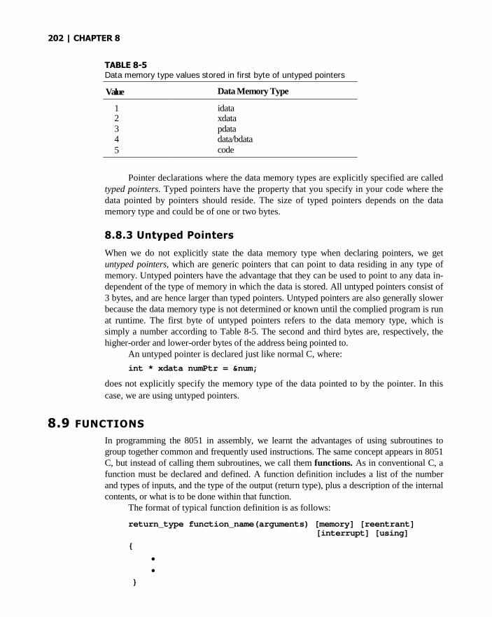
202 | CHAPTER 8
TABLE 8-5Data memory type values stored in first byte of untyped pointers
Value Data Memory Type
1 idata2 xdata3 pdata4 data/bdata5 code
Pointer declarations where the data memory types are explicitly specified are calledtyped pointers. Typed pointers have the property that you specify in your code where thedata pointed by pointers should reside. The size of typed pointers depends on the datamemory type and could be of one or two bytes.
8.8.3 Untyped Pointers
When we do not explicitly state the data memory type when declaring pointers, we getuntyped pointers, which are generic pointers that can point to data residing in any type ofmemory. Untyped pointers have the advantage that they can be used to point to any data in-dependent of the type of memory in which the data is stored. All untyped pointers consist of3 bytes, and are hence larger than typed pointers. Untyped pointers are also generally slowerbecause the data memory type is not determined or known until the complied program is runat runtime. The first byte of untyped pointers refers to the data memory type, which issimply a number according to Table 8-5. The second and third bytes are, respectively, thehigher-order and lower-order bytes of the address being pointed to.
An untyped pointer is declared just like normal C, where:
int * xdata numPtr = #
does not explicitly specify the memory type of the data pointed to by the pointer. In this
case, we are using untyped pointers.
8.9 FUNCTIONS
In programming the 8051 in assembly, we learnt the advantages of using subroutines togroup together common and frequently used instructions. The same concept appears in 8051C, but instead of calling them subroutines, we call them functions. As in conventional C, afunction must be declared and defined. A function definition includes a list of the numberand types of inputs, and the type of the output (return type), plus a description of the internalcontents, or what is to be done within that function.
The format of typical function definition is as follows:
return_type function_name(arguments) [memory] [reentrant][interrupt] [using]
{
}

8051 C PROGRAMMING | 203
where2
return_type refers to the data type of the return (output) valuefunction_name is any name that you wish to call the function asarguments is the list of the type and number of input (argument) valuesmemory refers to an explicit memory model (small, compact or large)reentrant refers to whether the function is reentrant (recursive)interrupt indicates that the function is actually an ISRUsing explicitly specifies which register bank to use
Consider a typical example, a function to calculate the sum of two numbers:
int sum(int a,int b)
{return a + b;}
This function is called sum and takes in two arguments, both of type int. The return type isalso int, meaning that the output (return value) would be an int. Within the body of the func-tion, delimited by braces, we see that the return value is basically the sum of the two ar-guments. In our example above, we omitted explicitly specifying the options: memory,reentrant, interrupt, and us ing. This means that the arguments passed to the function wouldbe using the default small memory model, meaning that they would be stored in internal datamemory. This function is also by default non-recursive and a normal function, not an ISR.Meanwhile, the default register bank used is bank 0.
8.9.1 Parameter Passing
In 8051 C, parameters are passed to and from functions and used as function arguments(inputs). Nevertheless, the technical details of where and how these parameters are stored aretransparent to the programmer, who does not need to worry about thesetechnicalitie2rheowever, we will briefly discuss in this section how parameters are passed inorder to appreciate how the compiler takes care of this on our behalf. In 8051 C, parametersare passed through the registers or through memory. Passing parameters through registers isfaster and is the default way in which things are done. The registers used and their purposeare described in more detail in Table 8-6.
TABLE 8-6Registers used in parameter passing
Number ofArgument
Char/1-BytePointer
INT/2-BytePointer Long/Float
GenericPointer
123
R7R5R3
R6 & R7R4 & R5R2 & R3
R4--R7R4-R7
R1-R3
2The statements delimited by square brackets indicate that they are optional.

204 | CHAPTER 8
TABLE 8-7
Registers used in returning values from functions
Return Type Register Description
Bitchar/unsigned char/1-byte pointerint/unsigned int/2-byte pointerlong/unsigned longfloatgeneric pointer
Carry Flag (C)R7R6&R7R4-R7R4-R7R1-R3
MSB in R6, LSB in R7 MSBin R4, LSB in R7 32-bit IEEEformat Memory type inR3,MSB in R2, LSB in R1
Since there are only eight registers in the 8051, there may be situations where we donot have enough registers for parameter passing. When this happens, the remaining param-eters can be passed through fixed memory locations. To specify that all parameters will bepassed via memory, the NOREGPARMs control directive is used. To specify the reverse,use the REGPARMs control directive.
8.9.2 Return Values
Unlike parameters, which can be passed by using either registers or memory locations,output values must be returned from functions via registers. Table 8-7 shows the registersused in returning different types of values from functions.
8.10 SOME 8051 C EXAMPLES
We have so far briefly covered the basic concepts of programming the 8051 in C. In thissection, we will look at various examples of how to write such programs. All the 8051 Cprograms discussed henceforth have been compiled and tested on Keil's µVision2, whichis an 8051 integrated development environment (IDE) that includes source code editing,compiling, and debugging.3
8.10.1 The First Program
As is customary in any introductory course on high-level, structured proi,amming languages,the first demonstrative example is a simple program that displays the message "Hello World,"
#include <REG51.H> /* SFR declarations */#include <stdio.h> /* Declarations for I/O
functions(eg. printf) */
main (){SCON = 0x52; /* serial port, mode 1 */
TMOD = 0x20; /* timer 1, mode 2 */
3A free evaluation version is available at http://www.keil.com.
8051 C PROGRAMMING | 205
TH1 = -13; /* reload count for 2400baud */
TR1 = 1; /* start timer 1 */
while (1) /* repeat forever */{printf ("Hello World\n"); /* Display "Hello World" */}
}
The program above continually displays the message "Hello World" to the device attachedto the serial port, which is by default connected to a simulated serial window. For furtherdetails about interacting with µVision2 IDE, refer to Appendix H or Keil's documentationsin µVision2's Help.
8.10.2 Timers
In Chapter 4, ideas of how to interact with the 8051's built-in timers were discussed. As abasis of comparison between programming the 8051 in assembly language and in C, wewill give here C solutions for some of the Chapter 4 examples.
EXAMPLE Pulse Wave Generation8.1 Write a program that creates a periodic waveform on P1.0 with as high a frequency as
possible.
Solution
#include <REGS1.H> /* SFR declarations */
shit portbit = Pl^0; /* Use variable portbit to refer toPi.0 */
main 0{while (1) /* repeat forever */
{portbit = 1; /* set P1.0 */portbit = 0; /* clear P1.0 */}
}
Discussion
This program is actually the C version for Example 4.2. In the program, port P1.0 needs tobe set and cleared repeatedly. This is done by simply writing a 1 and 0 to it. Since P1 hasalready been declared in the REG51.H header file, we can refer to its LSB by declaring anshit variable and using that in the main program.
There is one thing that we should note when making use of instructions to generatetiming delays and waveforms. In assembly, we could easily do so by taking note of how

206 | CHAPTER 8
many machine cycles it takes to execute a certain instruction. In C, however, it is cannotbe directly determined how long it would take to execute a certain statement, loop, orfunctions. All these depend on the specific C compiler used, since different compilers usedifferent levels of optimization and hence generate different combinations of assemblylanguage instructions and subsequently machine code.
The best way is to look at the specific assembly language instructions generated bythe compiler for a certain C statement and determine how many machine cycles they wouldtake. In µVision2 IDE, you can disassemble your C program into assembly language byviewing the Disassembly Window. Refer to Appendix H or Keil's Help documentation formore information.
EXAMPLE 10 kHz Square Wave8.2 Write a program using Timer 0 to create a 10kHz square wave on P1.0.
Solution
#include <REG51.H> /* SRR declarations */shit portbit = P1^0; /* Use variable portbit to
refer to Pi.H */
main ()
{TMOD = 2; /* 8-bit auto-reload mode */TH0 = -50; /* -50 reload value in TH0TR0 = 1; /* start timer 0 */
while (i) /* repeat forever */
{while (TF0 != 1); /* wait for overflow */TF0 = 0; /* clear timer overflow flag */portbit = !(portbit); /* toggle Pi.0 */}
}
Discussion
This is really the C version for Example 4.4. For an infinite loop, the while statement isused, with its condition a constant value of 1. In C, 1 denotes TRUE whereas a 0 denotesFALSE. Hence, in this case the condition would always be true, causing the whilestatement to be repeated indefinitely.
EXAMPLE 1 kHz Square Wave8.3 Write a program using Timer 0 to create a 1 kHz square wave on P1.0.
Solution
#include <REGS1.H> /* SFR declarations */sbit portbit = P1^0; /* Use variable portbit to
refer to Pi.0 */

8051 C PROGRAMMING | 207
main ()
{TMOD = 1; /* 16-bit timer mode */while (1) /* repeat forever */
{TH0 = 0xFE; /* -500 (high byte)TL0 = 0x0C; /* -500 (low byte)TR0 = 1; /* start timer 0 */while (TH0 != 1); /* wait for overflow */TR0 = 0; /* stop timer 0 */TF0 = 0; /* clear timer overflow flag */portbit = =(portbit); /* toggle Pi.0 */
}}
Discussion
This is the C version for Example 4.5 and is very similar to the previous example.
EXAMPLE Buzzer Interface8.4 A buzzer is connected to P1.7, and a debounced switch is connected to P1.6. Write a pro-
gram that reads the logic level provided by the switch and sounds the buzzer for 1 secondfor each 1-to-0 transition detected.
Solution
#include <REG51.H> /* SFR declarations */
int hundred = 100;
sbit inbit = P1^6; /* Use variable inbit to refer toP1.6 */
sbit outbit = P1^7; /* Use variable outbit to refer toPi.7 */
unsigned char R7; /* use 8-bit variable to representR7 */
void delay(void); /* Function prototype */main ()
{TMOD = 1; /* use timer 0 in mode 1 */while (1) /* repeat forever */
{while (inbit!=1); /* wait for 1 input*/while (inbit==1); /* wait for 0 input*/outbit = 1; /* turn buzzer on */delay(); /* wait for 1 second */outbit = 0; /* turn buzzer off */}
}

208 | CHAPTER 8
void delay(void)
{R7 = hundred;do
{TH0 = 0xD8; /* -10000 (high byte) */TL0= 0xF0; /* -10000 (low byte) */TR0 = 1;while (TF0 != 1);TF0 = 0;TR0 = 0;R7 -= 1;
while (R7!=0);}
Discussion
This example uses a function called delay() together with the main function. Since thefunction is defined after main, a on-line function prototype should be added prior to mainto allow the compiler to know that such a function exists. R7 is also not defined in theREG51.H header file, so it is defined here before being used in the delay() function. Thisis done to maintain direct correspondence to the assembly language solution of this ex-ample problem in Example 4.7. In reality when one programs in C, rather than using thegeneral purpose registers R0 to R7, one would simply declare variables instead. This isalso because the registers R0 to R7 are used by the compiler for parameter passing to andfrom functions.
8.10.3 Serial Port
In this section, we will give example solutions to the examples previously discussed inChapter 5 concerning the 8051 serial port.
EXAMPLE Initializing the Serial Port8.5 Write an instruction sequence to initialize the serial port to operate as an 8-bit UART at
2400 baud. Use Timer 1 to provide the baud rate clock.
Solution
#include <REG51> /* SFR declarations */
main (){
SCON = 0x52; /* serial port, mode 1 */TMOD = 0x20; /* timer 1, mode 2 */TH1 = -13; /* reload count for 2400 baud */TR1 = 1; /* start timer 1 */}

8051 C PROGRAMMING | 209
EXAMPLE Output Character Subroutine8.6 Write a function called OUTCHR to transmit the 7-bit ASCII code in the accumulator out
the 8051 serial port, with odd parity added as the 8th bit. Return from the function with theaccumulator intact.
Solution
#include <REG51.H> /* SFR declarations */
shit AccMSB = ACC^ 7; /* Use variable AccMSE to refer toACC.7 */
void OUTCHR(void){CY = P; /* put parity hit in C flag */CY = !CY; /* change to odd parity */AccMSB = CY; /* add to character code */while (TI != 1); /* Tx empty? no: check again */TI = 0; /* yes: clear flag and */SEUF = ACC; /* send character */AccMSB = 0; /* strip off parity hit */
}
Discussion
In the program, the MSB of the accumulator, ACC needs to be accessed so an shitvariable, AccMSE, is declared that refers to this MSB.
EXAMPLE Input Character Subroutine8.7 Write a function called INCHAR to input a character from the 8051's serial port and return
with the 7-bit ASCII code in the accumulator. Expect odd parity in the eighth bit receivedand set the carry flag if there is a parity error.
Solution
#include <REG51.H> /* SFR declarations */sbit AccMSB = ACC^7; /* Use variable AccMSB to refer to
ACC.7 */
void INCHAR(void)
{while (RI != 1); /* wait for character */RI = 0; /* clear flag */ACC = SBUF; /* read char into accumulator */CY = P; /* for odd parity in accumulator, P
should he set */CY = !CY; /* complementing correctly indicates ii
"error" */AccMSB = 0; /* strip off parity */
}

210 | CHAPTER 8
8.10.4 Interrupts
From our discussion of functions in Section 8.9, we know that interrupt service routines(ISRs) are written in very much the same way as normal functions, with the exception thatthe "interrupt" statement is used in the function definition. We will now show how the exam-ples from Chapter 6 on interrupts can be solved with programs written in 8051 C.
EXAMPLE Square Wave Using Timer Interrupts8.8 Write a program using Timer 0 and interrupts to create a 10 kHz square wave on P1.0.
Solution
#include <REG51.H> /* SFR declarations */
sbit portbit = P1^0; /* Use variable portbit to referto P1.0 */
main ()
{TMOD = 0x02; /* timer 0, mode 2 */
TH0 = -50; /* 50 ps delay */TR0 = 1; /* start timer */IE = 0x82; /* enable timer 0 interrupt */
while(1); /* repeat forever */
}
void T0ISR(void) interrupt 1{portbit = !portbit; /* toggle port hit Pi.0 */}
Discussion
This program introduces the use of an interrupt function, a special type of function that isautomatic whenever the corresponding interrupt occurs. Note that the interrupt statement isfollowed by an interrupt number, in this case, 1, which refers to a timer/counter 0 interrupt.Table 8-8 gives a list of the various interrupt numbers, types, and vector addresses.
EXAMPLE Two Square Waves Using Timer Interrupts8.9 Write a program using interrupts to simultaneously create kHz and 500Hz square waves
on P1.7 and P1.6.
Solution
#include <REG51.H> /* SFR declarations */
sbit portsev = P1^7; /* Use variable portsev to refer toP1.7 */
sbit portsix = P1^6; /* Use varibhle portsix to refer toP1.6 */

8051 C PROGRAMMING | 211
TABLE 8-8
Standard 8051 interrupts and interrupt numbers
Interrupt Number Description Vector Address
0 External INT 0 0003H1 Timer/Counter 0 000BH2 External INT 1 0013H3 Timer/Counter 1 0018H4 Serial Port 0023H
main (){TMOD = 0x12; /* timer 1, mode 1; twhile(i);ode 2 */
TH0 = -71; /* 7kHz using timer 0*/TR0 = 1; /* start timer */
TF1 = 1; /* force timer 1 interrupt */IE = 0x8A; /* enable both timer interrupts */while(1); /* repeat forever */}
void T0ISR(void) interrupt 1{portsev = !portsev; /* toghit Pi.6 bit P1.7 */}
void T1ISR(void) interrupt 3
{TR1 = 0;
TH1 = OxFC; /* 1 lms high time & */TL1 = 0x18; /* low time */TR1 = 1;
portsix = !portsix; /* toggle port bit P1.6 */}
Discussion
In this example, two interrupt functions are used to service Timer 0 and Timer 1 interrupts. As
can be seen from Table 8-8, the corresponding interrupt numbers are 1 and 3, respectively.
EXAMPLE Character Output Using Interrupts8.10 Write a program using interrupts to continually transmit the ASCII code set (excluding control
codes) to a terminal attached to the 8051's serial port.
Solution
#include <REG51.H> /* SFR declarations
*/ main()
{TMOD = 0x20; /* timer 1, mode 2 */TH1 = -26; /* 12000 baud reload value */
212 | CHAPTER 8
TR1 = 1; /* start timer */SCON = 0x42; /* mode 1, set TI to force 18t interrupt */ACC = 0x20; /* send ASCII space first */IE = 0x90; /* enahle serial port interrupt */while(1); /* repeat forever */
}
void SPISR(void) interrupt 4
{if (ACC == 0x7F) /* if finished ASCII set */
ACC = 0x20; /* reset to space */SBUF = ACC; /* send char. to serial port */ACC = ACC + 1; /* increment ASCII code */TI = 0; /* clear interrupt flag */
}
Discussion
This program uses an interrupt function to service a serial port interrupt request, where the interruptnumber used is 4. Note also that even though there is no restriction on what name you should usefor an interrupt function, the convention is to use explicit names such as SPISR and T0ISR to referto these interrupt functions.
EXAMPLE Furnace Controller8.11 Using interrupts, design an 8051 furnace controller that keeps a building at 20°C ± 1°C.
Solution
#include <REG51.H> /* SFR declarations */
sbit outbit = P1^7; /* Use variahle outbit to refer toP1.7 */
sbit hotbit = P3^2; /* Use variahle hotbit to refer to P3.2*/
main ()
{IE = 0x85; /* enahle external interrupts */IT0 = 1; /* negative edge triggered */IT1 = 1;outbit = 1; /* turn furnace on */if (hotbit != 1) /* if T > 21 degrees, */
outbit = 0; /* turn it off */while(1); /* repeat forever
*/
}
void EX0ISR(void) interrupt 0
{outhit = 0; /* turn furnace off */}

8051 C PROGRAMMING | 213
void EX0ISR(void) interrupt 2
{outbit = 1; /* turn furnace on */}
Discussion
Again, as this example shows, writing interrupt functions to service external interrupts issimilar to writing such functions for timer and serial port interrupts. The difference lies inthe interrupt numbers being used, which can be obtained from Table 8-8. Note again thatthe interrupt functions have been explicitly named.
EXAMPLE Intrusion Warning System
8.12 Design an intrusion warning system using interrupts that sounds a 400Hz tone for 1second (using a loudspeaker connected to P1.7) whenever a door sensor connected toINT0 makes a high-to-low transition.
Solution
#include <REG51.H> /* SFR declarations */
sbit outhit = P1^7; /* use variahle outhit to refer to P1.7 */unsigned char R7; /* use 8-bit variahle to represent R7 */
main()
{IT0 = 1; /* negative edge activated */TMOD = 0x11; /* 16-bit timer mode */
IE = 0x81; /* enable EXT 0 only */while(1); /* repeat forever */}
void T0ISR(void) interrupt 0{R7 = 20; /* 20 x 5000 µs = 1 second */
TF0 = 1; /* force timer 0 interrupt */TF1 = 1; /* force timer 1 interrupt */ET0 = 1; /* hegin tone for 1 second */ET1 = 1; /* enahle timer interrupts */
/* timer interrupts will do the work */}
void EX0ISR(void) interrupt 1
{TR0 = 0; /* stop timer */R7 = R7 - 1; /* decrement R7 */
if (R7 == 0) /* if 20th time, */
{ET0 = 0; /* disahle itself */ET1 = 0;}
214 | CHAPTER 8
else
{TH0 = 0x3C; /* 0.05 sec. delay */TL0 = 0xB0;
TR0 = 1;
}
}
void T1ISR(void) interrupt 3
{TR1 = 0;TH1 = 0xFB; /* count for 400 Hz*/TL1 = 0x1E;
outbit = !outbit; /* music maestro! */TR1 = 1;}
DiscussionThis is a combination of several interrupt functions previously discussed.
SUMMARY
This chapter has introduced the concepts of programming the 8051 in C, in contrast to previouschapters, which discussed programming the 8051 in assembly language. Nevertheless, whetherit be assembly language or C, both make it possible to write programs, especially complex onesin an organized manner, the structured way. This will be the topic of the next chapter.
PROBLEMS
8.1 How does the 8051 C language differ from the conventional C language in terms ofdata types?
8.2 Suppose you wish to declare a variable to store a bit value at physical bit address20H. Describe how you would do so in 8051 C.
8.3 What is the use of the carat (^) symbol in terms of bit addressable locations?8.4 In how many ways can you declare shit variables? Explain each way by giving
an example.8.5 What is the difference between an SFR and an unsigned char variable?8.6 Differentiate between the terms "memory types" and "memory models."8.7 Explain the difference between a function and an interrupt function.8.8 Explain, by giving an example, what you understand by a pointer.8.9 Suppose you would like to have most of your program variables residing in external
RAM while a few time-critical variables should reside in the first 128 bytes of in-ternal RAM. Briefly describe how you could achieve this.

8051 C PROGRAMMING | 215
8.10 Why is it not advisable to use the accumulator, ACC, when programming in C?8.11 Write a C program having numbers 1 to 10 in code memory, and that copies the odd (respectively
even) numbers to external data memory when P1.0 is set (respectively cleared).8.12 Write an 8051 C program to continually move a string of ASCII characters stored in internal data
memory at location 30H to external data memory at location 1234H.8.13 a. Show how you create a lookup table in code memory to store the first 10 values of the
function f (x) = ex+2 corresponding to x = {1, 2, ... , 10}.b. Next, declare a pointer that is stored in an indirectly accessible internal RAM location anduse that to obtain the value of f(2) and print it out on the screen.

216 | CHAPTER 8
Program Structure and Design
9.1 INTRODUCTION
What makes one program better than the next? Beyond simple views such as "it works,"the answer to this question is complex and depends on many factors: maintenance require-ments, computer language, quality of documentation, development time, program length,execution time, reliability, security, and so on. In this chapter we introduce the characteris-tics of good programs and some techniques for developing good programs. We begin withan introduction to structured programming techniques.
Structured programming is a technique for organizing and coding programs thatreduces complexity, improves clarity, and facilitates debugging and modifying. The idea ofproperly structuring programs is emphasized in most programming tasks, and we advance ithere as well. The power of this approach can be appreciated by considering the followingstatement: All programs may be written using only three structures. This seems too good tobe true, but it's not. "Statements," "loops," and "choices" form a complete set of structures,and all programs can be realized using only these three structures. Program control ispassed through the structures without unconditional branches to other structures. Eachstructure has one entry point and one exit point. Typically, a structured program contains ahierarchy of subroutines, each with a single entry point and a single exit point.1
The purpose of this chapter is to introduce structured programming as applied to as-sembly language programming and 8051 C programming. This is especially useful in thecontext of assembly language programming, since although high-level languages (such asPascal or C) promote structured programming through their statements (WHILE, FOR,etc.) and notational conventions (indentation), assembly language lacks such inherent pro-perties. Nevertheless, assembly language programming can benefit tremendously through
1In high-level languages, programs are composed of functions or procedures.
217
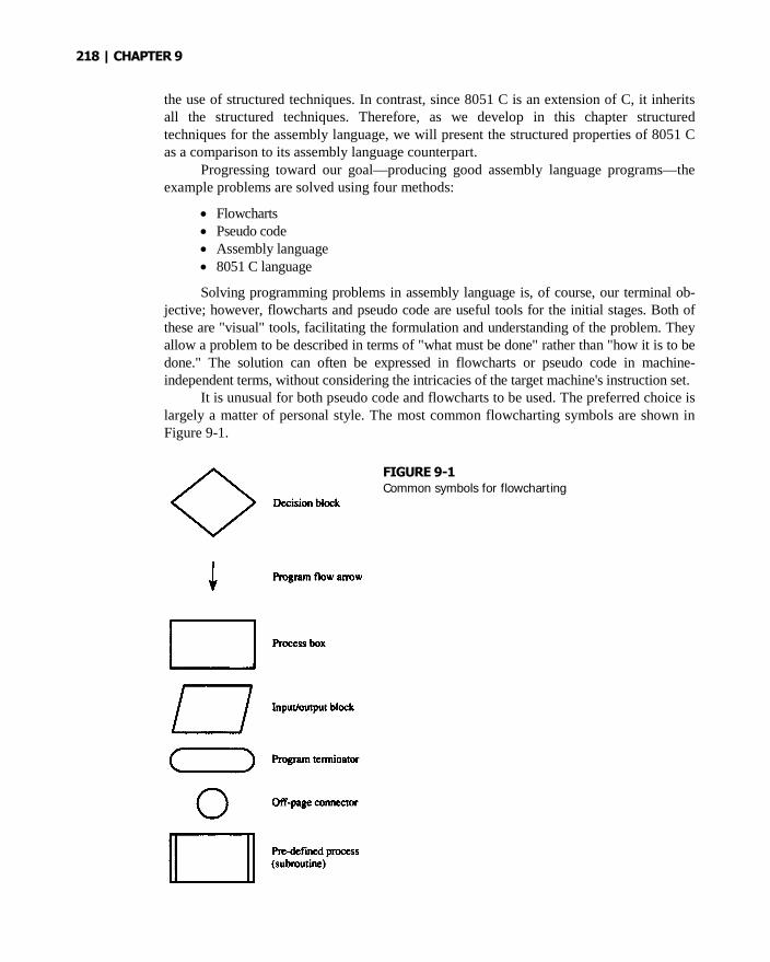
218 | CHAPTER 9
the use of structured techniques. In contrast, since 8051 C is an extension of C, it inheritsall the structured techniques. Therefore, as we develop in this chapter structuredtechniques for the assembly language, we will present the structured properties of 8051 Cas a comparison to its assembly language counterpart.
Progressing toward our goal—producing good assembly language programs—theexample problems are solved using four methods:
Flowcharts Pseudo code Assembly language 8051 C language
Solving programming problems in assembly language is, of course, our terminal ob-jective; however, flowcharts and pseudo code are useful tools for the initial stages. Both ofthese are "visual" tools, facilitating the formulation and understanding of the problem. Theyallow a problem to be described in terms of "what must be done" rather than "how it is to bedone." The solution can often be expressed in flowcharts or pseudo code in machine-independent terms, without considering the intricacies of the target machine's instruction set.
It is unusual for both pseudo code and flowcharts to be used. The preferred choice islargely a matter of personal style. The most common flowcharting symbols are shown inFigure 9-1.
FIGURE 9-1Common symbols for flowcharting

PROGRAM STRUCTURE AND DESIGN | 219
Pseudo code is just what the name suggests: "sort of a computer language. The ideahas been used informally in the past as a convenient way to sketch out solutions to pro-gramming problems. As applied here, pseudo code mimics the syntax of Pascal or C in itsnotation of structure, yet at the same time it encourages the use of natural language in de-scribing actions. Thus, statements such as
[get a character from the keyboard]
may appear in pseudo code. The benefit in using pseudo code lies in the strict adherence tostructure in combination with informal language. Thus we may see
IF [condition is true]THEN [do statement 1]ELSE BEGIN
[do statement 2][do statement 3]
END
o r
IF [the temperature is less than 20 degrees Celsius]THEN [wear a jacket]ELSE BEGIN
[wear a short sleeve shirt][bring sunglasses]
END
The use of keywords, indentation, and order is essential for the effective use of pseudocode. Our goal is to clearly demonstrate the solution to a programming problem usingflowcharts and/or pseudo code, such that the translation to assembly language is easierthan direct coding in assembly language. The final product is also easier to read, debug,and maintain. Pseudo code will be defined formally in a later section.
9.2 ADVANTAGES AND DISADVANTAGESOF STRUCTURED PROGRAMMING
The advantages of adopting a structured approach to programming are numerous. Theseinclude the following:
The sequence of operations is simple to trace, thus facilitating debugging. There are a finite number of structures with standardized terminology. Structures lend themselves easily to building subroutines. The set of structures is complete; that is, all programs can be written using three
structures. Structures are self-documenting and, therefore, easy to read. Structures are easy to describe in flowcharts, syntax diagrams, pseudo code, and so on. Structured programming results in increased programmer productivity—pro-
grams can be written faster.

220 | CHAPTER 9
However, some tradeoffs occur. Structured programming has disadvantages, such as thefollowing:
Only a few high-level languages (Pascal, C, PL/M) accept the structures directly;others require an extra stage of translation.
Structured programs may execute more slowly and require more memory than theunstructured equivalent.
Some problems (a minority) are more difficult to solve using only the three struc-tures rather than a brute-force "spaghetti" approach.
Nested structures can be difficult to follow.
9.3 THE THREE STRUCTURES
All programming problems can be solved using three structures:
Statements Loops Choice
The completeness of the three structures seems unlikely; but, with the addition ofnesting (structures within structures), it is easily demonstrated that any programming pro-blem can be solved using only three structures. Let's examine each in detail.
9.3.1 Statements
Statements provide the basic mechanism to do something. Possibilities include the simpleassigning of a value to a variable, such as
[count = 0]
or a call to a subroutine, such as
PRINT STRING("Select Option:")
Anywhere a single statement can be used, a group of statements, or astatement block, can be used. This is accomplished in pseudo code by enclosing thestatements between the keywords BEGIN and END as follows:
BEGIN
[statement 1]
[statement 2]
[statement 3]
END
Note that the statements within the statement block are indented from the BEGIN andEND keywords. This is an important feature of structured programming.
9.3.2 The Loop Structure
The second of the basic structures is the "loop," used to repeatedly perform an operation.Adding a series of numbers or searching a list for a value are two examples of programming

PROGRAM STRUCTURE AND DESIGN | 221
FIGURE 9-2
Flowchart for the WHILE/DO structure
problems that require loops. The term "iteration" is also used in this context. Although there areseveral possible forms of loops, only two are necessary, WHILE/DO and REPEAT/UNTIL.
9.3.2.1 The WHILE/DO Statement The WHILE/DO statement provides theeasiest means for implementing loops. It is called a "statement," since it is treated like astatement—as a single unit with a single entry point (the beginning) and a single exit point(the ending). The pseudo code format is Pseudo Code:
WHILE [condition] DO[statement]
The "condition" is a "relational expression" that evaluates to "true" or "false." If the con-dition is true, the statement (or statement block) following the "DO" is executed, and thenthe condition is reevaluated. This is repeated until the relational expression yields a falseresponse; this causes "statement" to be skipped, with program execution continuing at thenext statement. The WHILE/DO structure is shown in the flowchart in Figure 9-2.
EXAMPLE WHILE/DO Structure
9.1 Illustrate a WHILE/DO structure such that while the 8051 carry flag is set, a statement isexecuted.
Solution
Pseudo Code:
WHILE[c == 1]DO[statement]
(Note: The double equal sign is used to distinguish the relational operator, which tests forequality, from the assignment operator, the single equal sign [see 9.4 Pseudo Code Syntax].)

222|CHAPTER9
Flowchart:
9.2
Assembly Language:
ENTER: JNC EXITSTATEMENT: (statement)
JMP ENTER
EXIT: (continue)
8051 C:
while (c == 1){statement;}
As a general rule, the actions within the statement block must affect at least one variablein the relational expression; otherwise a bug in the form of an infinite loop results.
SUM Subroutine
FIGURE9-3Flowchart for Example 9.1
EXAMPLE
Write an 8051 subroutine called SUM to calculate the sum of a series of numbers.Parameters passed to the subroutine include the length of the series in R7 and the startingaddress of the series in R0. (Assume the series is in 8051 internal memory.) Return withthe sum in the accumulator.
Solution
Pseudo Code:
[sum = 0]WHILE [length > 0] DO BEGIN
[sum = sum + @pointer)[increment pointer][decrement length]
END

PROGRAM STRUCTURE AND DESIGN | 223
F
FF
lowchart:
IGURE 9-4
lowchart for Example 9.2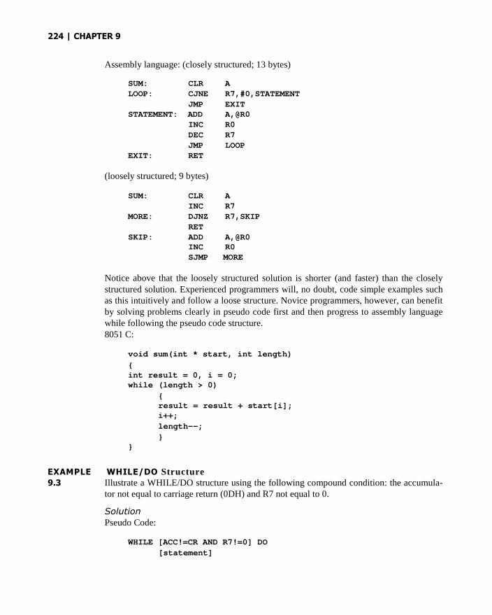
224 | CHAPTER 9
Assembly language: (closely structured; 13 bytes)
SUM: CLR ALOOP: CJNE R7,#0,STATEMENT
JMP EXITSTATEMENT: ADD A,@R0
INC R0DEC R7JMP LOOP
EXIT: RET
(loosely structured; 9 bytes)
SUM: CLR AINC R7
MORE: DJNZ R7,SKIPRET
SKIP: ADD A,@R0INC R0SJMP MORE
Notice above that the loosely structured solution is shorter (and faster) than the closelystructured solution. Experienced programmers will, no doubt, code simple examples suchas this intuitively and follow a loose structure. Novice programmers, however, can benefitby solving problems clearly in pseudo code first and then progress to assembly languagewhile following the pseudo code structure.8051 C:
void sum(int * start, int length)
{int result = 0, i = 0;while (length > 0)
{result = result + start[i];i++;
length--;
}}
EXAMPLE WHILE/DO Structure9.3 Illustrate a WHILE/DO structure using the following compound condition: the accumula-
tor not equal to carriage return (0DH) and R7 not equal to 0.
Solution
Pseudo Code:
WHILE [ACC!=CR AND R7!=0] DO
[statement]

PROGRAM STRUCTURE AND DESIGN | 225
Flowchart:
Assembly Language:
ENTER: CJNE A
JMP E
SKIP: CJNE R
JMP E
STATEMENT: one or
.
.
.JMP EN
EXIT: (contin
8051 C:
while( (ACC != C) &
statement;)
FIGURE 9-5
Flowchart for Example 9.3
,#0DH,SKIP
XIT
7,#0,STATEMENT
XIT
more statements)
TER
ue)
& (R7 != 0) )
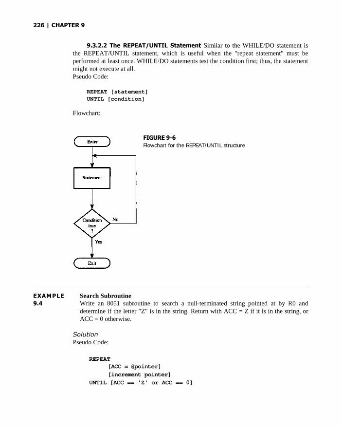
226 | CHAPTER 9
9.3.2.2 The REPEAT/UNTIL Statement Similar to the WHILE/DO statement isthe REPEAT/UNTIL statement, which is useful when the "repeat statement" must beperformed at least once. WHILE/DO statements test the condition first; thus, the statementmight not execute at all.Pseudo Code:
REPEAT [statement]UNTIL [condition]
Flowchart:
EXAMPLE
9.4
Search SubroutineWrite an 8051 subroutine to search a null-terminated string pointed at by R0 anddetermine if the letter "Z" is in the string. Return with ACC = Z if it is in the string, orACC = 0 otherwise.
Solution
Pseudo Code:
REPEAT[ACC = @pointer]
[increment pointer]
UNTIL [ACC == 'Z' or ACC == 0]
FIGURE 9-6
Flowchart for the REPEAT/UNTIL structure

PROGRAM STRUCTURE AND DESIGN | 227
Flowchart:
FIGURE 9-7
Assembly Language:
STATEMENT: MOV A,INC R0JZ EXCJNE A,
EXIT: RET
8051 C:
char statement(cha
{char a;do
{a = *start;start++;}
Flowchart for Example 9.4
@R0
IT#'Z',STATEMENT
r * start)

228 | CHAPTER 9
while ( (a != 'z') || (a != 0) );return a;
}
9.3.3 The Choice Structure
The third basic structure is that of "choice"—the programmer's "fork in the road." The twomost common arrangements are the IF/THEN/ELSE statement and the CASE statement.
9.3.3.1 The IF/THEN/ELSE Statement The IF/THEN/ELSE statement is usedwhen one of two statements (or statement blocks) must be chosen, depending on a con-dition. The ELSE part of the statement is optional.Pseudo Code:
IF [condition]THEN[statement 1]ELSE[statement 2]
Flowchart:
EXAMPLE
9.5
Character TestWrite a sequence of instructions to input and test a character from the serial port. If thecharacter is displayable ASCII (i.e., in the range 20H to 7EH), echo it as is; otherwise,echo a period (.).
FIGURE 9-8Flowchart for the IF/THEN/ELSE
structure

PROGRAM STRUCTURE AND DESIGN | 229
SolutionPseudo Code:
[input character]IF [character == graphic]
THEN [echo character]
ELSE [echo '.']
Flowchart:
Assembly Language: (closel
ENTER: ACAACAJNC
STMENT1: ACAJMP
STMENT2: MOVACA
EXIT: (co
FIGURE 9-9Flowchart for Example 9.5
y structured; 14 bytes)
LL INCHLL ISGRPH
STMENT2LL OUTCHR
EXITA,#'.'
LL BUTCHERntinue)

230 | CHAPTER 9
(loosely structured; 10 bytes)
ACALL INCHACALL ISGRPHJC SKIPMOV A,#'.'
SKIP: ACALL OUTCHR(continue)
8051 C:
while (1)
{char a;
a = inchar();
if (isgrph(a))
outchr(a);
elseoutchar(`.');
}
Modify the structure to repeat indefinitely:
WHILE [1] DO BEGIN
[input character]
IF [character == graphic]
THEN [echo character]
ELSE [echo '.']
END
9.3.3.2 The CASE Statement The CASE statement is a handy variation of theIF/THEN/ELSE statement. It is used when one statement from many must be chosen asdetermined by a value.Pseudo Code:
CASE [expression] OF
0:[statement 0]
1:[statement 1]
2:[statement 2]
.
.
.
n:[statement n]
[default statement]
END_CASE
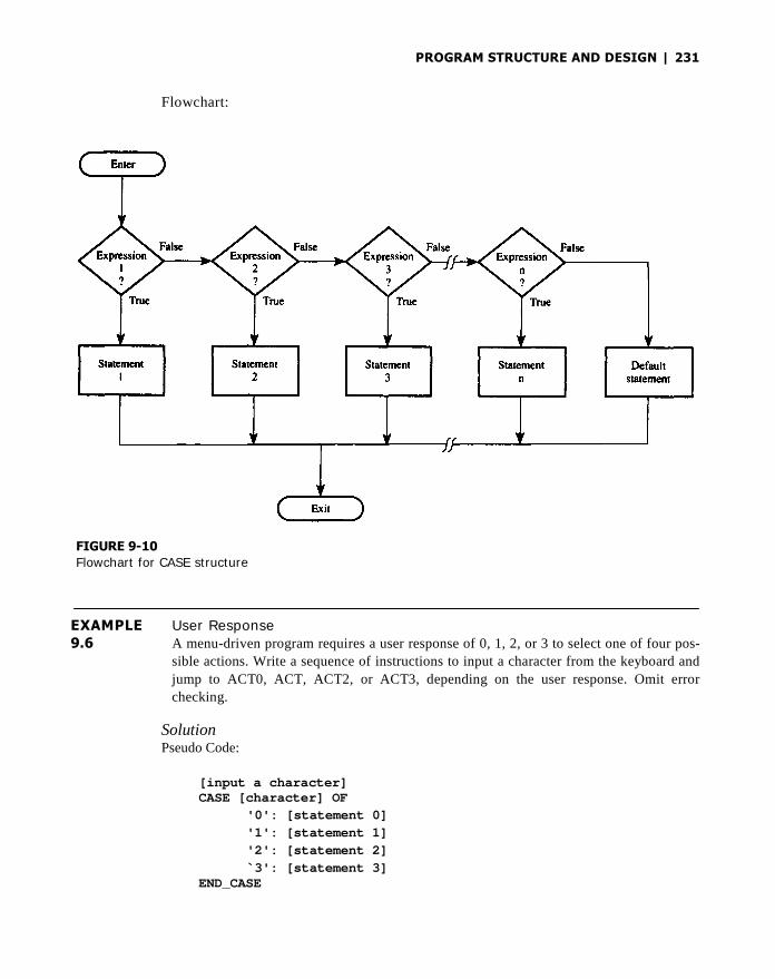
PROGRAM STRUCTURE AND DESIGN | 231
Flowchart:
FIGURE 9-10
Flowchart for CASE structure
EXAMPLE User Response
9.6 A menu-driven program requires a user response of 0, 1, 2, or 3 to select one of four pos-
sible actions. Write a sequence of instructions to input a character from the keyboard and
jump to ACT0, ACT, ACT2, or ACT3, depending on the user response. Omit error
checking.
SolutionPseudo Code:
[input a character]CASE [character] OF
'0': [statement 0]
'1': [statement 1]
'2': [statement 2]
`3': [statement 3]END_CASE

232 | CHAPTER 9
Flowchart:
FIGURE 9-11
Flowchart for Example 9.6
Assembly Language: (closely structured)
CALL INCHCJNE A,#'0',SKIP1
ACT0: .
.
.JMP EXIT
SKIP: CJNE A,#'1',SKIP2ACT: .
.
.JMP EXIT
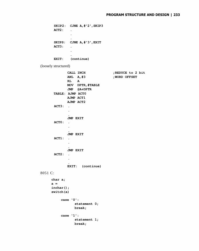
PROGRAM STRUCTURE AND DESIGN | 233
SKIP2: CJNE A,#'2',SKIP3ACT2: .
.
.SKIPS: CJNE A,#'3',EXITACT3: .
.
.EXIT: (continue)
(loosely structured)
CALL INCH ;REDUCE to 2 bitANL A,#3 ;WORD OFFSETRL AMOV DPTR,#TABLEJMP @A+DPTR
TABLE: AJMP ACT0AJMP ACT1AJMP ACT2
ACT3: .
.
.JMP EXIT
ACT0: .
.
.JMP EXIT
ACT1: .
.
.JMP EXIT
ACT2: .
.
.EXIT: (continue)
8051 C:
char a;a =inchar();switch(a)
case '0':statement 0;break;
case '1':statement 1;break;

234 | CHAPTER 9
case '2':statement 2;break;
case '3':statement 3;
}
9.3.3.3 The GOTO Statement GOTO statements can always be avoided by usingthe structures just presented. Some times a GOTO statement provides an easy method ofterminating a structure when errors occur; however, exercise extreme caution. When theprogram is coded in assembly language, GOTO statements usually become unconditionaljump instructions. A problem will arise, for example, if a subroutine is entered in the usualway (a CALL subroutine instruction), but is exited using a jump instruction rather than areturn from subroutine instruction. The return address will be left on the stack, and eventu-ally a stack overflow will occur.
9.4 PSEUDO CODE SYNTAX
Since pseudo code is similar to a high-level language such as Pascal or C, it is worthwhiledefining it somewhat more formally, so that, for example, a pseudo code program can bewritten by one programmer and converted to assembly language by another programmer.
We should acknowledge too that pseudo code is not always the best approach for de-signing programs. While it offers the advantage of easy construction on a word processor(with subsequent modifications), it suffers from a disadvantage common to other program-ming languages: pseudo code programs are written line-by-line, so parallel operations are notimmediately obvious. With flowcharts, on the other hand, parallel operations can be placedphysically adjacent to one another, thus improving the conceptual model (see Figure 9-10).
Before presenting a formal syntax, the following tips are offered to enhance thepower of solving programming problems, using pseudo code.
Use descriptive language for statements. Avoid machine dependencies in statements. Enclose conditions and statements in brackets: [ ]. Begin all subroutines with their names followed by a set of parentheses: 0. Pa-
rameters passed to subroutines are entered (by name or by value) within theparentheses.
End all subroutines with RETURN followed by parentheses. Return values are en-tered within the parentheses.
Examples of subroutines:
INCHAR ()[statement]
. . .RETURN (char)
OUTCHR(char) STRLEN(pointer)[statement] [statement]
. . . . . .RETURN ( ) RETURN(length)

PROGRAM STRUCTURE AND DESIGN | 235
Use lowercase text except for reserved words and subroutine names. Indent all statements from the structure entry and exit points. When a LOOP or
CHOOSE structure is started, the statements within the structure appear at the nextlevel of indentation.
Use the commercial at sign (@) for indirect addressing.
The following is a suggested syntax for pseudo code.
Reserved Words:
BEGIN ENDREPEAT UNTILWHILE DOIF THEN ELSECASE OFRETURN
Arithmetic Operators:
+ addition- subtraction
* multiplication/ division
% modulus (remainder after division)
Relational Operators: (result is true or false)
== true if values equal to each other
!= true if values not equal< true if first value less than second<= true if first value <= second value
> true if first value > second value>= true if first value >= second value&& true if both values are true|| true if either value is true
Bitwise Logical Operators:
& logical AND| logical OR^ logical exclusive OR~ logical NOT (one's complement)>> logical shift right<< logical shift left
Assignment Operators:
= set equal to
op = assignment operation shorthand where "op" is oneof + - * / << >> & ^ |e.g.: j += 4 is equivalent to j = j + 4

236 | CHAPTER 9
Precedence Operation:
( )
Indirect Address:
@
Operator Precedence:
( )~ @
* / %+ -<< >>< <= > >=
== !=
&
|&&
||
= += -= *= etc.
Note 1. Do not confuse relational operators with bitwise logical operators. Bitwise logicaloperators are generally used in assignment statements such as
[lower_nibble = byte & 0FH]
whereas relational operators are generally used in conditional expressions such as
IF [char 1= 'Q' && char !=0DH] THEN ...
Note 2. Do not confuse the relational operator "= =" with the assignment operator "=." For
example, the Boolean expression
j = = 9
is either true or false depending on whether or not j is equal to the value 9, whereas the
assignment statement
j = 9
assigns the value 9 to the variable j.
Structures:Statement:
[do something]
Statement Block:
BEGIN[statement]
PROGRAM STRUCTURE AND DESIGN | 237
[statement]. . .
END
WHILE/DO:
WHILE [condition] DO[statement]
REPEAT/UNTIL:
REPEAT
[statement]UNTIL [condition]
IF/THEN/ELSE:
IF [condition]
THEN [statement 1]ELSE [statement 2])
CASE/OF:
CASE [expression] OF1:[statement1]2:[statement2]3:[statement3]
.
.
.n:[statement n]
[default statement]END_CASE
9.5 ASSEMBLY LANGUAGE PROGRAMMING STYLE
It is important to adopt a clear and consistent style in assembly language programming. This is
particularly important when one is working as part of a team, since individuals must be able to
read and understand each other's programs.
The assembly language solutions to problems up to this point have been deliberately
sketchy. For larger programming tasks, however, a more critical approach is required. The
following tips are offered to help improve assembly language programming style.
9.5.1 Labels
Use labels that are descriptive of the destination they represent. For example, when
branching back to repeatedly perform an operation, use a label such as "LOOP," "BACK,"
"MORE," etc. When skipping over a few instructions in the program, use a label such

238 | CHAPTER 9
as "SKIP" or "AHEAD." When repeatedly checking a status bit, use a label such as"WAIT" or "AGAIN."
The choice of labels is restricted somewhat when one is using a simple memory-resident or absolute assembler. These assemblers treat the entire program as a unit, thuslimiting the use of common labels. Several techniques circumvent this problem. Commonlabels can be sequentially numbered, such as SKIP, SKIP, SKIP3 , etc.; or perhaps withinsubroutines all labels can use the name of the subroutine followed by a number, such asSEND, SEND2, SEND3, etc. There is an obvious loss of clarity here, since the labelsSEND2 and SEND3 are not likely to reflect the skipping or looping actions taking place.
More sophisticated assemblers, such as ASM51, allow each subroutine (or acommon group of subroutines) to exist as a separate file that is assembled independent ofthe main program. The main program is also assembled on its own and then combinedwith the subroutines using a linking and locating program that, among other things,resolves external references between the files. This type of assembler, usually called a"relocatable" assembler, allows the same label to appear in different files.
9.5.2 Comments
The use of comments cannot be overemphasized, particularly in assembly language pro-gramming, which is inherently abstract. All lines of code, except those with truly obviousactions, should include a comment.
Conditional jump instructions are effectively commented using a question similar tothe flowchart question for a similar operation. The "yes" and "no" answers to the questionshould appear in comments at the lines representing the "jump" and "no jump" actions. Forexample, in the INLINE subroutine below, note the style of comments used to test for thecarriage return <CR>code.
; *************************************************************;; INPUT LINE OF CHARACTERS; INLINELINE MUST END WITH <CR>; MAXIMUM LENGTH 31 CHARACTERS INCLUDE <CR>;ENTER: NO CONDITIONS
;EXIT: ASCII CODES IN INTERNAL DATA RAM; 0 STORED AT END OF LINE;USES INCHAR, OUTCHR;; *************************************************************;INLINE: PUSH 00H ;SAVE R0 ON STACK
PUSH 07H ;SAVE R7 ON STACKPUSH ACC ;SAVE ACCUMULATOR ON STACKMOV R0,#60H ;SET UP BUFFER AT 60HMOV R7,#31 ;MAXIMUM LENGTH OF LINE
STMENT: ACALL INCHAR ;INPUT A CHARACTER
ACALL OUTCHR ;ECHO TO CONSOLE

PROGRAM STRUCTURE AND DESIGN | 239
MOV @R0,A ;STORE IN BUFFERINC RE ;INCREMENT BUFFER POINTERDEC R7 ;DECREMENT LENGTH COUNTERCJNE A,#0DH, SKIP ;IS CHARACTER = <CR>?SJMP EXIT ;YES: EXIT
SKIP: CJNE R7,#0,STMENT ;NO: GET ANOTHER CHARACTEREXIT: MOV @R0,#0
POP ACC ;RETRIEVE REGISTERS FROM;STACK
POP 07HPOP 00HRET
9.5.3 Comment Blocks
Comment lines are essential at the beginning of each subroutine. Since subroutinesperform well-defined tasks commonly needed throughout a program, they should begeneral-purpose and well documented. Each subroutine is preceded by a comment block,a series of comment lines that explicitly state
The name of the subroutine The operation performed Entry conditions Exit conditions Name of other subroutines used (if any) Name of registers affected by the subroutine (if any)
The INLINE subroutine above is a good example of a well-commented subroutine.
9.5.4 Saving Registers on the Stack
As applications grow in size and complexity, new subroutines are often written that buildupon and use existing subroutines. Thus, subroutines are calling other subroutines, whichin turn call other subroutines, and so on. These are called "nested subroutines." There isno danger in nesting subroutines so long as the stack has enough room to hold the returnaddresses. This is not a problem, since nesting beyond several levels is rare.
A potential problem, however, lies in the use of registers within subroutines. As thehierarchy of subroutines grows, it becomes more and more difficult to keep track of whatregisters are affected by subroutines. A solid programming practice, then, is to save regis-ters on the stack that are altered by a subroutine, and then restore them at the end of thesubroutine. Note that the INLINE subroutine shown above saves and retrieves R0, R7, andthe accumulator using the stack. When INLINE returns to the calling subroutine, theseregisters contain the same value as when INLINE was called.
9.5.5 The Use of Equates
Defining constants with equate statements makes programs easier to read and maintain.Equates appear at the beginning of a program to define constants such as carriage return

240 | CHAPTER 9
(<CR>) and line feed (<LF>), or addresses of registers inside peripheral ICs such as STA-TUS or CONTROL.
The constant can be used throughout the program by substituting the equated symbol forthe value. When the program is assembled, the value is substituted for the symbol. A generoususe of equates makes a program more maintainable, as well as more readable. If a constant mustbe changed, only one line needs changing—the line where the symbol is equated. When the pro-gram is reassembled, the new value is automatically substituted wherever the symbol is used.
9.5.6 The Use of Subroutines
As programs grow in size, it is important to "divide and conquer"; that is, subdivide largeand complex operations into small and simple operations. These small and simple opera-tions are programmed as subroutines. Subroutines are hierarchical in that simple subrou-tines can be used by more complex subroutines, and so on.
A flowchart references a subroutine using the "predefined process" box. (See Figure9-1.) The use of this symbol indicates that another flowchart elsewhere describes thedetails of the operation.
Subroutines are constructed in pseudo code as complete sections of code, beginning withtheir names and parentheses. Within the parentheses are the names or values of parameterspassed to the subroutine (if any). Each subroutine ends with the keyword RETURN followed byparentheses containing the name or value of parameters returned by the subroutine (if any).
Perhaps the simplest example of subroutine hierarchy is the output stung(OUTSTR) and output character (OUTCHR) subroutines. The OUTSTR subroutine (ahigh-level routine) calls the OUTCHR subroutine (a low-level routine).
The flowcharts, pseudo code, and 8051 assembly and C language solutions areshown below.
Pseudo Code:
OUTCHR (char)[put odd parity in bit 7]REPEAT [test transmit buffer]UNTIL [buffer empty][clear transmit buffer empty flag][move char to transmit buffer]
[clear parity bit]RETURN ()OUTSTR (pointer)
WHILE [(char = @pointer) !=0] BEGINOUTCHR (char)[increment pointer]
ENDRETURN()
Assembly language:
OUTCHR: MOV C,P ;PUT PARITY BIT IN C FLAGCPL C ;CHANGE TO ODD PARITYMOV ACC.7,C ;ADD TO CHARACTER
AGAIN: JNB TI,AGAIN ;TX EMPTY?

PROGRAM STRUCTURE AND DESIGN | 241
CLR TI ;YES: CLEAR FLAG ANDMOV SBUF,A ; SEND CHARACTERCLR ACC.7 ;STRIP OFF PARITY BIT ANDRET ; RETURN
OUTCHR: MOV A,@DPTR ;GET CHARACTERJZ EXIT ;IF 0, DONE
CALL OUTSTR ;OTHERWISE SEND ITINC DPTR ;INCREMENT POINTERSJMP OUTCHR ; AND GET NEXT CHARACTER
EXIT: RET
Flowchart:
FIGURE 9-12Flowchart for OUTCHR subroutine

242 | CHAPTER 9
8051C
sbit AccMSB = ACC^7;void outchr (char a)
{ACC = a;CY = P;
CY = !CY;AccMSB = CY;while (TI != 1);TI = 0;SBUF = ACC;AccMSB = 0;
}void outstr(char * msg)
{while (*msg !='\0')
outchr(*p++);}
FIGURE 9-13Flowchart for OUTSTR subroutine

PROGRAM STRUCTURE AND DESIGN | 243
9.5.7 Program Organization
Although programs are often written piecemeal (i.e., subroutines are written separatelyfrom the main program), all programs should be consistent in their final organization. Ingeneral, the sections of a program are ordered as follows:
Equates Initialization instructions Main body of program Subroutines Data constant definitions (DB and DW) RAM data locations defined using the DS directive
All but the last item above are called the "code segment" and the RAM data locations arecalled the "data segment." Code and data segments are traditionally separate, since code isoften destined for ROM or EPROM, whereas RAM data are always destined for RAM.Note that data constants and strings defined using the DB or DW directives are part of thecode segment (not the data segment), since these data are unchanging constants and, there-fore, are part of the program.
9.6 8051 C PROGRAMMING STYLE
When programming in 8051 C, it is even more necessary to be clear and consistent. This isbecause programmers usually write in C when their 8051 programs are large and complex,and involve several programmers working on it at the same time. The following should benoted when programming the 8051 in C.
9.6.1 Comments
In C, comments are enclosed in between the /* and */ symbols. For example, the com-mented "Hello World" program is given below:
main (){SCON = 0x52; /* perial port, mode 1 */TMOD = 0x20; /* timer 1, mode 2 */TH1 = -13; /* reload count for 2400 baud */TR1 = 1; /* start timer 1 */while (1) /* repeat forever */
{printf ("Hello World\n"); /* Dipplay "Hello World" */}
}

244 | CHAPTER 9
9.6.2 The Use of Defines
You should define constants with aliases so that your program is more readable and it is easierfor you to change the constant in future by simply changing one line of code. For example:
#define PI 3.1415927#define MAX 10
int circleArea(int radiup){return (PI * radius * radius);}
main(){int i;for (i = 0; i < MAX; i++)
circleArea(i);}
The example program above defines PI as the constant = 3.1415927 while MAX is de-fined as the constant number 10. PI is used to calculate the area of a circle while MAX isthe maximum number of different circle areas that are being calculated. If, for example,one desires to calculate areas of 20 different circles, then the value of MAX can be changedby simply changing the definition line to #define MAX 20.
9.6.3 The Use of Functions
C programs, being large and complex, are normally written by several programmerssimultaneously. This is possible by using the modular programming approach, whichbreaks parts of the program into modules and functions. Dividing the program intofunctions allows for more modularity and makes the overall program clearer and easier tofollow. This approach has been adopted in the interface and design example programsdiscussed in Chapter 12.
9.6.4 The Use of Arrays and Pointers
When it is desired to store a sequence of some related data, it is good to use arrays and havethem pointed to by pointers. Recall that pointers store addresses of memory locations.Hence, the address of the first element of an array could be assigned to a pointer. Then eacharray element could be accessed by adding a suitable offset to the pointer value and deref-erencing it. As an example, lookup tables can be optimally implemented by using arrays.
Arrays are also useful when storing strings. For example, the message "This is awelcome message" could be stored in memory as an array by simply using the line: char* MSG = {"Thip is a welcome message." } which would use an array ofcharacters to store the string.

PROGRAM STRUCTURE AND DESIGN | 245
9.6.5 Program Organization
To standardize the layout and organization, we have adopted the following program organization whenwriting 8051 C programs:
Includes Constant Definitions Variable Definitions Function Prototypes Main Function Function Definitions
Constant definitions are lines such as #define PI 3.1415927 while variable definitions are those suchas char A. Function prototypes are one-line statements such as void HTOA (void) that consist of thefunction name, return type, and parameter list. Meanwhile, function definitions are the full definitions ofoperations done in the functions, for example:
void HTOA(void) {A = A & 0xF; if(A>=0xA)
A = A + 7;A = A + '0';}
SUMMARY
This chapter has introduced structured programming techniques through flowcharting and pseudo code.Suggestions were offered on designing and presenting programs to enhance their readability. In the nextchapter, some of the tools and techniques for developing programs are presented.
PROBLEMS
9.1 Illustrate a WHILE/DO structure such that while the accumulator is less than or equal to 7EH, astatement block is executed.
9.2 Illustrate a WHILE/DO structure using the following compound condition: (accumulator greaterthan zero and R7 greater than zero) or the carry flag equal to 1. Treat the values in the accumulatorand R7 as unsigned integers.
9.3 Write a subroutine to find the place of the most significant 1 in the accumulator. Return with"place" in R7. For example, if ACC = 00010000B, return with R7 = 4.
9.4 Write a subroutine called INLINE to input a line of characters from the console and place them ininternal memory, starting at location 60H. Maximum line length is 31 characters, including thecarriage return. Put 0 at the end of the line.

246 | CHAPTER 9

Tools and Techniques forProgram Development
10.1 INTRODUCTION
In this chapter, the process of developing microcontroller- or microprocessor-based pro-ducts is described as it follows a series of steps and utilizes a variety of tools. Inprogressing from concept to product, numerous steps are involved and numerous tools areused. The most common steps and tools are presented as found in typical design scenariosemploying the 8051 microcontroller.
Design is a highly creative activity, and in recognition of this we state at the outsetthat substantial leeway is required for individuals or development teams. Such autonomymay be difficult to achieve for very large or safety-critical projects, however. Admittedly,in such environments the management of the process and the validation of the results mustsatisfy a higher order. The present chapter addresses the development of relatively small-scale products, such as controllers for microwave ovens, automobile dashboards,computer peripherals, electronic typewriters, or high-fidelity audio equipment.
The steps required and the tools and techniques available are presented and elabo-rated on, and examples are given. Developing an understanding of the steps is important,but strict adherence to their sequence is not advocated. It is felt that forcing the develop-ment process along ordered, isolated activities is usually overstressed and probably wrong.Later in the chapter we will present an all-in-one development scenario, where the avail-able resources are known and called upon following the instinct of the designer. We beginby examining the steps in the development cycle.
10.2 THE DEVELOPMENT CYCLE
Proceeding from concept to product is usually shown in a flow diagram known as thedevelopment cycle, similar to that shown in Figure 10-1. The reader may notice that
247

248 | CHAPTER 10
FIGURE 10-1
The development cycle
there is nothing particularly "cyclic" about the steps shown. Indeed, the figure shows theideal and impossible scenario of "no breakdowns." Of course, problems arise. Debugging(finding and fixing problems) is needed at every step in the development cycle withcorrections introduced by reengaging in an earlier activity. Depending on the severity ofthe error, the correction may be trivial or, in the extreme, may return the designer to theconcept stage. Thus, there is an implied connection in Figure 10-1 from the output of anystep in the development cycle to any earlier step.
The steps along the top path in Figure 10-1 correspond to software development,while those along the bottom correspond to hardware development. The two paths meet ata critical and complicated step called "integration and verification," which leads to accept-ance of the design as a "product." Not shown are various steps subsequent to acceptance ofthe design. These include, for example, manufacturing, testing, distribution, andmarketing. The dotted line in Figure 10-1 encompasses the steps of primary concern in thischapter (and book). These will be elaborated in more detail later. But first, we begin byexamining the steps in software development.
10.2.1 Software Development
The steps in the top path in Figure 10-1 are discussed in this section, beginning with thespecification of the application software.
Specifying Software. Specifying software is the task of explicitly stating what the soft-ware will do. This may be approached in several ways. At a superficial level,specifications may first address the user interface; that is, how the user will interact withand control the system. (What effects will result from and be observed for each actiontaken?) If switches, dials, or audio or visual indicators are employed on the prototypehardware, the explicit purpose and operation of each should be stated.

TOOLS AND TECHNIQUES FOR PROGRAM DEVELOPMENT | 249
Formal methods have been devised by computer scientists for specifying softwarerequirements; however, they are not generally used in the design of microcontroller-basedapplications, which are small in comparison to application software destined for main-frame computers.
Software specifications may also address details of system operation below the user level.For example, a controller for a photocopier may monitor internal conditions necessary for nor-mal or safe operation, such as temperature, current, voltage, or paper movement. These condi-tions are largely independent of the user interface but still must be accommodated by software.
Specifications can be modularized by system function with entry and exit conditionsdefined to allow intermodule communication. The techniques described in the previouschapter for documenting subroutines are a reasonable first step in specifying software.
Interrupt-driven systems require careful planning and have unique characteristics thatmust be addressed at the specification stage. Activities without time-critical requirementsmay be placed in the foreground loop or in a round-robin sequence for handling by timedinterrupts. Time-critical activities generate high-priority interrupts that take over the systemfor immediate handling. Software specifications may emphasize execution time on suchsystems. How long does each subroutine or interrupt service routine (ISR) take to execute?How often is each ISR executed? ISRs that execute asynchronously (in response to anevent) may take over the system at any time. It may be necessary to block them in some in-stances or to preempt (interrupt) them in others. Software specifications for such systemsmust address priority levels, polling sequences, and the possibility of dynamically reas-signing priority levels or polling sequences within ISRs.
Designing Software. Designing the software is a task designers are likely to jump intowithout a lot of planning. There are two common techniques for designing software priorto coding: flowcharts and pseudo code. These were the topic of Chapter 9.
Editing and Translation. The editing and translation of software occur, at least initially, ina tight cycle. Errors detected by the assembler are quickly corrected by editing the sourcefile and reassembling. Since the assembler has no idea of the purpose of the program andchecks only for "grammatical" errors (e.g., missing commas, undefined instructions), theerrors detected are syntax errors. They are also called assemble-time errors.
Preliminary Testing. A run-time error will not appear until the program is executed by asimulator or in the target system. These errors may be elusive, requiring careful observation ofCPU activity at each stage in the program. A debugger is a system program that executes a userprogram for the purpose of finding run-time errors. The debugger includes features such asexecuting the program until a certain address (a breakpoint) is reached, and single-steppingthrough instructions while displaying CPU registers, status bits, or input/output ports.
10.2.2 Hardware Development
For the most part, this book has not emphasized hardware development. Since the 8051 isa highly integrated device, we have focused on learning the 8051's internal architectureand exploiting its on-chip resources through software. The examples presented thus farhave used only simple interfaces to external components.

250 | CHAPTER 10
Specifying Hardware. Specifying the hardware involves assigning quantitative data tosystem functions. For example, a robotic arm project should be specified in terms of numberof articulations, reach, speed, accuracy, torque, power requirements, and so on. Designers areoften required to provide a specification sheet analogous to that accompanying an audio am-plifier or VCR. Other hardware specifications include physical size and weight, CPU speed,amount and type of memory, memory map assignments, I/O ports, optional features, etc.
Designing Hardware. The conventional method of hardware design, employing a penciland a logic template, is still widely used but may be enhanced through computer-aideddesign (CAD) software. Although many CAD tools are for the mechanical or civil engi-neering disciplines, some are specifically geared for electronic engineering. The two mostcommon examples are tools for drawing schematic diagrams and tools for laying outprinted circuit hoards (PCBs). Although these programs have a long learning curve, theresults are impressive. Some schematic drawing programs produce files that can be readby PCB programs to automatically generate a layout.
Building the Prototype. There are pathetically few shortcuts for the labors of prototyp-ing. Whether breadboarding a simple interface to a bus or port connector on a single-board computer (SBC), or wire wrapping an entire controller board, the techniques ofprototyping are only developed with a great deal of practice. Large companies with largebudgets may proceed directly to a printed circuit board format, even for the first iterationof hardware design. Projects undertaken by small companies, students, or hobbyists,however, are more likely to use the traditional wire wrapping method for prototypes.
Preliminary Testing. The first test of hardware is undertaken in the absence of any ap-plication software. Step-wise testing is important: there's no point in measuring a clocksignal using an oscilloscope before the presence of power-supply voltages has beenverified. The following sequence may be followed:
Visual checks Continuity checks DC measurements AC measurements
Visual and continuity checks should occur before power is applied to the board. Con-tinuity checks using an ohmmeter should be conducted from the IC side of the prototype,from IC pin to IC pin. This way, the IC pin-to-socket and socket pin-to-wire connection areboth verified. ICs should be removed when power is first applied to the prototype. DCvoltages should be verified throughout the board with a voltmeter. Finally, AC measurementsare made with the ICs installed to verify clock signals, and so on.
After verifying the connections, voltages, and clock signals, debugging becomespragmatic: Is the prototype functioning as planned? If not, corrective action may take thedesigner back to the construction, design, or specification of the hardware.
If the design is a complete system with a CPU, a single wiring error may prevent theCPU from completing its reset sequence: The first instruction after reset may never exe-cute! A powerful debugging trick is to drive the CPU's reset line with a low frequencysquare wave ( kHz) and observe (with an oscilloscope or logic analyzer) bus activityimmediately following reset.

TOOLS AND TECHNIQUES FOR PROGRAM DEVELOPMENT | 251
Functional testing of the board may require application software or a monitor pro-gram to "work" the board through its motions. It is at this stage that software must assist incompleting the development cycle.
10.3 INTEGRATION AND VERIFICATION
The most difficult stage in the development cycle occurs when hardware meets software.Some very subtle bugs that eluded simulation (if undertaken) emerge under real-time exe-cution. The problem is confounded by the need for a full complement of resources: hard-ware such as the PC development system, target system, power supply, cables, and testequipment; and software such as the monitor program, operating system, terminal emula-tion program, and so on.
We shall elaborate on the integration and verification step by first expanding thearea within the dotted line in Figure 10-1. (See Figure 10-2.)
Figure 10-2 shows utility programs and development tools within circles, user fileswithin squares, and "execution environments" within double-lined squares. The use of aneditor to create a source file is straightforward. The translation step (from Figure 10-1) isshown in two stages. An assembler (e.g., ASM51) converts a source file to an object file,and a linker/locator (e.g., RL51) combines one or more relocatable object files into a sin-gle absolute object file for execution in a target system or simulator. The assembler andlinker/locator also create listing files.
The most common filename suffixes are shown in parentheses for each file type. Al-though any filename and suffix usually can be provided as an argument, assemblers varyin their choice of default suffixes.
If the program was written originally in a single file following an absolute format,linking and locating are not necessary. In this case, the alternate path in Figure 10-2 showsthe assembler generating an absolute object file.
It is also possible (although not emphasized in this book) that high-level languages,such as C or PL/M, are used instead of, or in addition to, assembly language. Translation re-quires a cross-compiler to generate the relocatable object modules for linking and locating.
A librarian may also participate, such as Intel's LIB51. Relocatable object modulesthat are general-purpose and useful for many projects (most likely subroutines) may bestored in "libraries." RL51 receives the library name as an argument and searches the li-brary for the code (subroutines) corresponding to previously declared external symbolsthat have not been resolved at that point in linking/locating.
10.3.1 Software Simulation
Five execution environments are shown in Figure 10-2. Preliminary testing (see Figure 10-1)proceeds in the absence of the target system. This is shown in Figure 10-2 as software sim-ulation. A simulator is a program that executes on the development system and imitates thearchitecture of the target machine. An 8051 simulator, for example, would contain a fictitious(or "simulated") register for each of the special function registers and fictitious memorylocations corresponding to the 8051's internal and external memory spaces. Programs

FIGURE 10-2
Detailed steps in the development cycle
TOOLS AND TECHNIQUES FOR PROGRAM DEVELOPMENT | 253
are executed in simulation mode with progress presented on the development system'sCRT display. Simulators are useful for early testing; however, portions of the applicationprogram that directly manipulate hardware must be integrated with the target system fortesting.
10.3.2 Hardware Emulation
A direct connection between the development system and the target system is possiblethrough a hardware emulator (or in-circuit emulator). The emulator contains a proces-sor that replaces the processor IC in the target system. The emulator processor, however,is under the direct control of the development system. This allows software to execute inthe environment of the target system without leaving the development system. Commandsare available to single-step the software, execute to a breakpoint (or the nth occurrence of abreakpoint), and so on. Furthermore, execution is at full speed, so time-dependent bugsmay surface that eluded debugging under simulation.
The main drawback of hardware emulators is cost. PC-hosted units sell in the $2,000to $7,000 (U.S.) range, which is beyond the budget of most hobbyists and stretches thebudgets of most colleges or universities (if equipping an entire laboratory, for example).Companies supporting professional development environments, however, will not hesitateto invest in hardware emulators. The benefit in accelerating the product developmentprocess easily justifies the cost.
10.3.3 Execution from RAM
An effective and simple scenario for testing software in the target system is possible, evenif a hardware emulator is not available. If the target system contains external RAM config-ured to overlap the external code space (using the method discussed in Chapter 2; see 2.6.4,Data Pointer), then the absolute object program can be transferred, or "downloaded," fromthe development system to the target system and executed in the target system.
Intel Hexadecimal Format. As shown in Figure 10-2, an extra stage of translation isrequired to convert the absolute object file to a standard ASCII format for transmission.Since object files contain binary codes, they cannot be displayed or printed. Thisweakness is alleviated by splitting each binary byte into two nibbles and converting eachnibble to the corresponding hexadecimal ASCII character. For example, the byte 1AHcannot be transmitted to a printer because in ASCII it represents a control character ratherthan a graphic character. However, the bytes 31H and 41H can be transmitted to a printerbecause they correspond to graphic or displayable ASCII codes. In fact, these two byteswill print as "1A." (See Appendix F.)
One standard for storing machine language programs in .a displayable or printableformat is known as "Intel hexadecimal format." An Intel hex file is a series of lines or"hex records" containing the following fields:
Field Bytes Description
Record mark 1 ":"indicates start-of-recordRecord length 2 number of data bytes in record

254 | CHAPTER 10
Load address 4 starting address for data bytesRecord type 2 00 = data record; 01 = end recordData bytes 0-16 dataChecksum 2 sum of all bytes in record +
checksum = 0
These fields are shown in the Intel hexadecimal file in Figure 10-3. Conversion programs areavailable that receive an absolute object program as input, convert the machine languagebytes to Intel hexadecimal format, and generate a hex file as output. Intel's conversion utilityis called OH.
10.3.4 Execution from EPROM
Once a satisfactory degree of performance is obtained through execution in RAM (orthrough in-circuit emulation), the software is burned into EPROM and installed in the sys-tem as firmware. Two types of EPROMs are identified in Figure 10-2 as examples. The8751 is the EPROM version of the 8051, and the 2764 is a common, general-purposeEPROM used in many microprocessor- or microcontroller-based products. Systems de-signed using an 8751 benefit in that Ports 0 and 2 are available for I/O, rather than func-tioning as the address and data buses. However, 8751s are relatively expensive comparedto 2764s ($30 versus $5, for example).
10.3.5 The Factory Mask Process
If a final design is destined for mass production, then a cost-effective alternative to EPROMis a factory mask ROM, such as the 8051. An 8051 is functionally identical to an 8751; how-ever, code memory cannot be changed on an 8051. The data are permanently entered duringthe IC manufacturing cycle using a "mask"-essentially a photographic plate that passes or
FIGURE 10-3
Intel hexadecimal format

TOOLS AND TECHNIQUES FOR PROGRAM DEVELOPMENT | 255
masks (i.e., blocks) light during a stage of manufacturing. Connections to memory cells inthe 8051 are either made or blocked, thus programming each cell as a 1 or 0.
The choice of using an 8751 versus an 8051 is largely economic. A factory maskdevice is considerably cheaper than the EPROM device; however, there is a large setupfee to produce the mask and initiate a custom manufacturing cycle. A tradeoff point can beidentified to determine the feasibility of each approach. For example, if 8751s sell for $25and 8051s sell for $5 plus a $5,000 setup fee, then the break-even point is
25 n = 5 n + 500020 n = 5000
n = 250 units
A production run of 250 units or more would justify the use of the 8051 over the 8751.The situation is more complicated when comparing designs using an 8051 versus an
8031 + 2764, for example. In the latter case, the 8031 + 2764 alternative is much cheaperthan an 8751 with on-chip EPROM, so the tradeoff point occurs at much greaterquantities. If an 8031 + 2764 sells for, say, $7, then the break-even point is
7 n = 5 n + 50002 n = 5000
n = 2500 units
A production run of 1000 units would not justify use of the 8051—or so it seems. The use ofexternal EPROM means that Ports 0 and 2 are unavailable for I/O. This may be a critical pointthat prevents the 8031 + 2764 approach. Even if the loss of on-chip I/O is not a concern, otherfactors enter. The 8031 + 2764 approach requires two ICs instead of one. This complicatesmanufacturing, testing, maintenance, reliability, procurement, and a host of other seemingly in-nocent, but nevertheless real, dimensions of product design. Furthermore, the 8031 + 2764design will be physically larger than the 8051 design. If the final product necessitates a smallform factor, then the 8051 may have to be used, regardless of the additional cost.
10.4 COMMANDS AND ENVIRONMENTS
In this section the overall development environment is considered. We present the notionthat at any time the designer is working within an "environment" with commands doingthe work. The central environment is the operating system on the host system, which ismost likely MS-DOS running on a member of the PC family of microcomputers. Assuggested in Figure 10-4, some commands return to MS-DOS upon completion, whileothers evoke a new environment.
Invoking Commands. Commands are either resident (e.g., DIR) or transient (e.g.,FORMAT, DISKCOPY). A resident command is in memory at all times, ready for execu-tion (e.g., DIR). A transient command is an executable disk file that is loaded intomemory for execution (e.g., FORMAT).
Application programs are similar to transient commands in that they exist as an exe-cutable disk file and are invoked from the MS-DOS prompt. However, there are still manypossibilities. Commands or applications may be invoked as part of a batch file, by a func-tion key, or from a menu-driven user interface acting as a front-end for MS-DOS.

256 | CHAPTER 10
FIGURE 10-4The development environment
If command arguments are needed, there are many possibilities again. Although argu-ments are typically entered on the invocation line following the command, somecommands have default values for arguments, or prompt the user for arguments.Unfortunately, there is no standard mechanism, such as the "dialogue box" used in theMacintosh interface, to retrieve extra information needed for a command or application.
Some applications, such as editors, "take over" the system and bring the user into anew environment for subsequent activities.
Environments. As evident in Figure 10-4, some software tools such as the simulator, in-circuit emulator, or EPROM programmer evoke their own environment. Learning the nuances
TOOLS AND TECHNIQUES FOR PROGRAM DEVELOPMENT | 257
of each takes time, due to the great variety of techniques for directing the activities of theenvironment: cursor keys, function keys, first-letter commands, menu highlighting, defaultpaths, and so on. It is often possible to switch among environments while leaving them ac-tive. For example, terminal emulators and editors usually allow switching to DOSmomentarily to execute commands. The MS-DOS command EXIT immediately brings theuser back the suspended environment.
Methodology. As research in artificial intelligence and cognitive science has discovered,modeling human "problem solving" is a slippery business. Humans appear to approach theelements of a situation in parallel, simultaneously weighing possible actions and proceeding byintuition. The methodology suggested here recognizes this human quality. The steps in thedevelopment cycle and the tools and techniques afforded by the development environmentshould be clearly understood, but the overall process should support substantial freedom.
The basic operation of commands is to "translate," "view," or "evoke" (a new environ-ment). The results of translation should be viewed to verify results. We can take the attitude ofnot believing the outcome of any translation (assembling, EPROM programming, etc.) andverify everything by viewing results. Tools for viewing are commands such as DIR (Were theexpected output files created?), TYPE (What's in the output file?), EDIT, PRINT, and so on.
SUMMARY
The tools and techniques available for designing microcontroller-based products havebeen introduced in this chapter. There is no substitute for experience, however. Success indesign requires considerable intuition, a valuable commodity that cannot be delivered in atextbook. The age-old expression "trial and error" still rings true as the main techniqueemployed by designers for turning ideas into real products.
PROBLEMS
10.1 If 8751 EPROMs sell for $30 in any quantity and a mask-programmed 8051 sellsfor $3 plus a $10,000 setup fee, how many units are necessary to justify use of the8051 device? What is the savings for projected sales of 3,000 units of the finalproduct if the 8051 is used instead of the 8751?
10.2 Below is an 8051 program in Intel hex format.
a. What is the starting address of the program?b. What is the length of the program?c. What is the last address of the program?
258 | CHAPTER 10
10.3 The following is a single line from an Intel hex file with an error in the checksum.The incorrect checksum appears in the last two characters as "00." What is the cor-rect checksum?
10.4 The contents of an Intel hex file are shown below.
Recreate the original source program that this file represents.

Design and Interface Examples
11.1 INTRODUCTION
Many of the 8051's hardware and software features are brought together in this chapterthrough several design and interface examples. The first is an 8051 single-board computer—the SBC-51—suitable for learning about the 8051 or developing 8051-based products. TheSBC-51 uses a substantial monitor program offering basic commands for system operationand user interaction. The monitor program (MON51) is described in detail in Appendix G.
The interface examples are advanced in comparison to those presented in previouschapters. Each example includes a hardware schematic, a statement of the designobjective, a software listing of a program that achieves the design objective, and a generaldescription of the operation of the hardware and software. The software listings areextensively commented and should be consulted for specific details.
11.2 THE SBC-51
Several companies offer 8051 single-board computers similar to that described in thissection. Surprisingly, the basic design of an 8051 single-board computer does not varysubstantially among the various products offered. Since many features are "on-chip,"designing an 8051 single-board computer is straightforward. For the most part, only thebasic connections to external memory and the interface to a host computer are required.
A monitor program in EPROM is also required. The most basic system requirements,such as examining and changing memory locations or downloading application programsfrom a host computer, are needed to get "up and running." The SBC-51 described hereworks together with a simple monitor program to provide these basic functions.
259
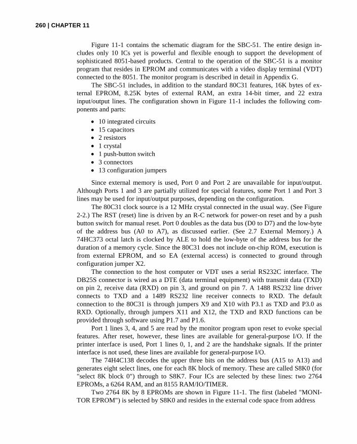
260 | CHAPTER 11
Figure 11-1 contains the schematic diagram for the SBC-51. The entire design in-cludes only 10 ICs yet is powerful and flexible enough to support the development ofsophisticated 8051-based products. Central to the operation of the SBC-51 is a monitorprogram that resides in EPROM and communicates with a video display terminal (VDT)connected to the 8051. The monitor program is described in detail in Appendix G.
The SBC-51 includes, in addition to the standard 80C31 features, 16K bytes of ex-ternal EPROM, 8.25K bytes of external RAM, an extra 14-bit timer, and 22 extrainput/output lines. The configuration shown in Figure 11-1 includes the following com-ponents and parts:
10 integrated circuits 15 capacitors 2 resistors 1 crystal 1 push-button switch 3 connectors 13 configuration jumpers
Since external memory is used, Port 0 and Port 2 are unavailable for input/output.Although Ports 1 and 3 are partially utilized for special features, some Port 1 and Port 3lines may be used for input/output purposes, depending on the configuration.
The 80C31 clock source is a 12 MHz crystal connected in the usual way. (See Figure2-2.) The RST (reset) line is driven by an R-C network for power-on reset and by a pushbutton switch for manual reset. Port 0 doubles as the data bus (D0 to D7) and the low-byteof the address bus (A0 to A7), as discussed earlier. (See 2.7 External Memory.) A74HC373 octal latch is clocked by ALE to hold the low-byte of the address bus for theduration of a memory cycle. Since the 80C31 does not include on-chip ROM, execution isfrom external EPROM, and so EA (external access) is connected to ground throughconfiguration jumper X2.
The connection to the host computer or VDT uses a serial RS232C interface. TheDB25S connector is wired as a DTE (data terminal equipment) with transmit data (TXD)on pin 2, receive data (RXD) on pin 3, and ground on pin 7. A 1488 RS232 line driverconnects to TXD and a 1489 RS232 line receiver connects to RXD. The defaultconnection to the 80C31 is through jumpers X9 and X10 with P3.1 as TXD and P3.0 asRXD. Optionally, through jumpers X11 and X12, the TXD and RXD functions can beprovided through software using P1.7 and P1.6.
Port 1 lines 3, 4, and 5 are read by the monitor program upon reset to evoke specialfeatures. After reset, however, these lines are available for general-purpose I/O. If theprinter interface is used, Port 1 lines 0, 1, and 2 are the handshake signals. If the printerinterface is not used, these lines are available for general-purpose I/O.
The 74H4C138 decodes the upper three bits on the address bus (A15 to A13) andgenerates eight select lines, one for each 8K block of memory. These are called S8K0 (for"select 8K block 0") through to S8K7. Four ICs are selected by these lines: two 2764EPROMs, a 6264 RAM, and an 8155 RAM/IO/TIMER.
Two 2764 8K by 8 EPROMs are shown in Figure 11-1. The first (labeled "MONI-TOR EPROM") is selected by S8K0 and resides in the external code space from address

FIGURE 11-1a
An 8051 single-board computer—the SBC-51 (a) Processor and serial port interface; (b) Address
decoding, RAM, and EPROM; (c) 8155 and power connections
261

FIGURE 11-1bcontinued
262
DESIGN AND INTERFACE EXAMPLES | 263
FIGURE 11-1c
continued

264 | CHAPTER 11
0000H to 1FFFH. Since the SBC-51 will begin execution from address 0000H
immediately after a system reset, the monitor program must reside in this IC. The second
2764 is labeled "USER EPROM" and is selected by S8K1 for execution at addresses 2000H
to 3FFFH. This IC is intended for user applications and is not needed for basic system
operation. Note that both EPROMs are selected only if CE (chip enable; pin 20) is active (or
low) and OE is also active (or low). OE is driven by the 80C31's PSEN line; thus selection
is in the external code space, as expected.
The 6264 8K by 8 RAM IC is selected by S8K4 (if jumper X6 is installed, asshown), so it resides at addresses 8000H to 9FFFH. The RAM is selected to occupy boththe external data space and the external code space using the method described earlier.(See Section 2.7.4 Overlapping the External Code and Data Spaces.) This dual occupancyallows user programs to be loaded (or written) to the RAM as "data memory" and thenexecuted as "code memory."
The 8155 RAM/IO/TIMER is a peripheral interface IC that was added to
demonstrate the expansion capabilities of the SBC-51. It is easy to add other peripheral
interface ICs in a similar way. The 8155 is selected by S8K0 placing it at the bottom of
memory. No conflict occurs with the monitor EPROM (which also resides at the bottom
of memory, but in the external code space) because the 8155 is further selected for read
and write operations using RD and WR .The 8155 contains the following features:
256 bytes of RAM 22 input/output lines 14-bit timer
Address line A8 connects to the 8155's IO/ M line (pin 7) and selects the RAM when lowand the I/O lines or timer when high. The I/O lines and timer are accessed from six ad-dresses, so the total address range of the 8155 is 0000H to 0105H (256 + 6 addresses).These are summarized below.
Address Purpose
0000H first RAM addressOther RAM addresses
OOFFH last RAM address
0100H Interval/command register0101H Port A0102H Port B0103H Port C0104H Low-order 8 bits of timer count0105H High-order 6 bits of timer count & 2 bits of
timer mode
Although the manufacturer's data sheet should be consulted for details of the 8155's ope-ration, configuring the I/O ports is extremely easy. By default all port lines are inputs aftera system reset; therefore, no "initialize" operation is needed to read input devices

DESIGN AND INTERFACE EXAMPLES | 265
connected to the 8155. To read Port A into the accumulator, for example, the followinginstruction sequence is used:
MOV DPTR,#0100H ;DPTR points to 8155 Port AMOVX A,@DPTR ;read Port A into Acc
To program Port A and Port B as outputs, is must first be written into the command registerbits 0 and 1, respectively. For example, to configure Port B as an output port and leave PortA and Port C as input, the following instruction sequence is used:
MOV DPTR,#0100H ;8155 command register
MOV A,#0000001OB ;Port B = output
MOVX @DPTR,A ;initialize 8155
Port C is configured as an output by writing 1s to the command register bits 2 and 3. Allthree ports would be configured as output as follows:
MOV DPTR,#0100H ;8155 command register
MOV A,#00001111B ;all ports = output
MOVX @DPTR ;initialize 8155
Port A of the 8155 is shown connected to a 20-pin header labeled "Centronics printerinterface." This interface is for demonstration purposes only. MON51 includes a PCHAR(print character) subroutine and directs output to the VDT and a parallel printer ifCONTROL-Z is entered on the keyboard. (See Appendix G.) Of course, Port A can be usedfor other purposes if desired.
Power-supply connections are also shown in Figure 11-1. The filter capacitorsare particularly important for the +5 volt supply to avoid glitches due to inductive ef-fects when digital devices switch. If the SBC-51 is constructed on a prototype board(for example, by wire wrapping), these capacitors should be considered critical. Place a10 µF electrolytic capacitor where power enters the prototype board, and 0.01 µF ce-ramic capacitors beside the socket for each IC, wired between the +5 volt pin and theground pin.
Since the SBC-51 is small and inexpensive, it is easy to construct a prototype andgain hands-on experience through the monitor program and the interfacing examples in thischapter. Wire wrapping is the most practical method of construction. The SBC-51 is alsoavailable assembled and tested on a printed-circuit board (see Figure 11-2).
This concludes our description of the SBC-51. The following sections contain exam-ples of interfaces to peripheral devices that have been developed to connect to the SBC-51(or a similar 8051 single-board computer).
11.3 HEXADECIMAL KEYPAD INTERFACE
Interfaces to keypads are common for microcontroller-based designs. Keypad inputand LED output are an economical choice for a user interface and are often adequate

266|CHAPTER11
FIGURE11-2The printed-circuit board version of the SBC-51 (Courtesy URDA, Inc.)
for complex applications. Examples include the user interface to microwave ovens orautomated banking machines. Figure 11-3 shows an interface between Port 1 and ahexadecimal keypad. The keypad contains 16 keys arranged in four rows and four columns.The row lines are connected to Port 1 bits 4-7, the column lines to Port 1 bits 0-3.
FIGURE11-3Interface to hexadecimal keypad

DESIGN AND INTERFACE EXAMPLES | 267
EXAMPLE Design Objective
11.1 Write a program that continually reads hexadecimal characters from the keypad and echoesthe corresponding ASCII code to the console.
On the surface, this example seems quite simple. The software can be divided intothe following steps:
1. Get a hexadecimal character from the keypad.2. Convert the hexadecimal code to ASCII.3. Send the ASCII code to the VDT.4. Go to step 1.
In fact, the software solution shown in Figure 11-4 follows this exact pattern (seelines 16-19). Of course, the work is done in the subroutines. Note that steps 2 and 3 aboveare implemented by calling subroutines in MON51. Of course, the code could have beenextracted from MON51 and placed in the listing in Figure 11-4, but that's wasteful. In-stead, the MON51 entry points for these subroutines are defined near the top of the listing(in lines 12-13) using the symbols HTOA and OUTCHR, and then the subroutines arecalled in the MAIN program loop in the usual way. Incidentally, the entry points forMON51 subroutines can be found in the symbol table created by RL51 when MON51 waslinked and located. The entry points for HTOA and OUTCHR, for example, are found inAppendix G.
The real challenge for this example is writing the subroutines IN_HEX and
GET_KEY. GET_KEY does the work of scanning the row and column lines of the key
pad to determine if a key is pressed. If no key is pressed, it returns with C = 0. If a key is
pressed, it returns with C = 1 and the hexadecimal code for the key in the accumulator bits
0-3.
IN_HEX performs software debouncing. Since the keypad is a series of mechanical
switches, contact closure and release include bounce—the rapid but brief make-and-break
of the switch contacts. Debouncing is performed by calling GET_HEX repeatedly until 50
consecutive calls return with C = 1. Any call to GET_HEX returning with C = 0 is inter-
preted as noise (i.e., bounce) and the counter is reset. After detecting a legitimate key clo-
sure, IN_HEX then waits for 50 consecutive calls to GET_HEX returning with C = 0. This
ensures a clean key release before the next call to GET_HEX.The software in Figure 11-4 works, but it is not particularly elegant. Since interrupts
are not used, the program's utility within a larger application is limited. A reasonable im-provement, therefore, is to redesign the software, using interrupts. An interrupt-driven in-terface is illustrated in the next example.
11.4 INTERFACE TO MULTIPLE 7-SEGMENT LEDS
An interface to a 7-segment LED display was presented in a problem at the end ofChapter 3. (See Figure 3-8.) Unfortunately, the interface used seven lines on Port 1,so it represents a poor allocation of the 8051's on-chip resources. In this section, we

FIGURE 11-4a
Software for keypad interface
268
DESIGN AND INTERFACE EXAMPLES | 269
FIGURE 11-4b
continued
demonstrate an interface to four 7-segment LEDs using only three of the 8051's I/O lines.This, obviously, is a much-improved design, particularly if multiple segments must beconnected.
Central to the design is the Motorola MC14499 7-segment decoder/driver, which in-cludes much of the circuitry necessary to drive four displays. The only additional componentsare a 0.015 µF timing capacitor, seven 47 Ohm current-limiting resistors, and four 2N3904transistors. Figure 11-5 shows the connections between the 80051, the MC14499, and the four7-segment LEDs.
EXAMPLE Design Objective
11.2 Assume BCD digits are stored in internal RAM locations 70H and 71H. Copy the BCD dig-its to the LED display 10 times per second using interrupts.
The software to accomplish the above objective is shown in Figure 11-6. The list-ing illustrates a number of concepts discussed earlier. The low-level details of sendingdata to the MC14499 are found in the subroutines UPDATE and OUTS. At a higherlevel, this example illustrates the design of interrupt-driven applications with a signifi-cant amount of foreground and background activity (unlike the examples in Chapter 6,which operated only in the background). The interrupts for this example coexist withMON51, which does not itself use interrupts. The monitor program executes in theforeground while the program in Figure 11-6 executes at interrupt-level in thebackground. When the program is started (e.g., by entering the MON51 commandGO8000; see Appendix G), conditions are initialized for the necessary interrupt-initiated updating of the LED displays, and then control quickly passes back to themonitor program. Monitor commands can be executed in the usual way; meanwhile,interrupts are occurring in the background. If, for example, the monitor SET commandis used to change internal RAM locations 70H and 71H, the changes are seenimmediately (within 0.1 s) on the 7-segment LED displays.Note the overall structure of the program. The following sections appear in order:
Assembler controls (lines 1-3) Comment block (lines 4-30)
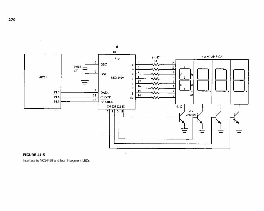
270
FIGURE 11-5
Interface to MC14499 and four 7-segment LEDs

FIGURE 11-6a
Software for MC14499 interface
271

272 | CHAPTER 11
FIGURE 11-6bcontinued

DESIGN AND INTERFACE EXAMPLES | 273
Definition of symbols (lines 31-38) Define storage declarations (lines 40-42) Jump table for program and interrupt entry points (lines 44-51) Main section (MAIN; lines 56-69) External interrupt service routine (EXTOISR; lines 74-77) Update LED display subroutine (UPDATE; lines 89-97) Output byte subroutine (OUT8; lines 103-113) Code to handle unimplemented interrupts (lines 118-123)
The program is written for execution at address 8000H in the SBC-5l's 6264 RAM IC.Since interrupts vector through locations at the bottom of memory, the monitor programincludes a jump table redirecting interrupts to addresses starting at address 8000H. (SeeAppendix G.) The program entry point is conveniently 8000H; however, an LJMP in-struction (line 45; see Figure 11-6) passes control to the label MAIN. All the initializeinstructions are contained in lines 56-68. The MAIN section terminates by jumping backthe monitor program.
11.5 INTERFACE TO LIQUID CRYSTAL DISPLAYS (LCDS)
The previous section saw the use of 7-segment LEDs for display purposes. The 7-segmentdisplay is sufficient for displaying numbers and simple characters but some more complexcharacters require the use of other alternatives such as the liquid crystal display (LCD).One very popular application of LCDs is in scientific calculators. In this section, we willshow how to interface to a simple LCD consisting of two lines of 16 characters, eachcharacter formed by a 5 x 7 dot matrix. Most LCDs are compatible with the de factoHitachi HD44780 standard. The connections between the 8051 and an HD44780-compatible LCD are straightforward and are shown in Figure 11-7.
FIGURE 11-7Interface to an LCD

274 | CHAPTER 11
EXAMPLE Design Objective11.3 Assume that ASCII characters are stored in internal RAM locations 30H-7FH. Write a pro-
gram to continually display these characters on the LCD, 16 characters at a time.
The software listing for this is in Figure 11-8. As previously shown in Figure 11-7,
the LCD has three control lines: Register Select (RS), Read/Write (R/ W ), and Enable (E).
When RS = 0, a command word is to be sent to the LCD while if RS = 1, a data word
would be sent
FIGURE 11-8aSoftware for LCD interface

DESIGN AND INTERFACE EXAMPLES | 275
FIGURE 11-8bcontinued

276 | CHAPTER 11
TABLE 11-1
LCD command codes
Code Description
1 Cleardisplay screen2 Return tohomeposition4 Shift cursor to left5 Shift display right6 Shift cursor to right7 Shift display left8 Display off, cursor offA Display off, cursor onC Display on, cursor offE Display on, cursor blinkingF Display on, cursor not blinking10 Shift cursor to left14 Shift cursor to right18 Shift entire display to left1C Shift entire display to right80 Forcecursor tobeginningof1
stline
C0 Force cursor to beginningof2nd line38 2 lines, 5 X 7 matrix display
instead. R/ W = 1 means that the 8051 would be reading from the LCD whereas R/ W = 0means that the 8051 is writing to the LCD. Finally, E has to be set high and then brought low tosignal to the LCD that its attention is required to process the command or data currently avail-able at its data pins. Table 11-1 shows the command codes that could be issued to the LCD.
The software first calls an INIT subroutine to initialize the display modes andsettings before proceeding to display on the LCD a sequence of 16 ASCII characters at atime. Notice that before sending any data to the LCD, a WAIT subroutine is called first towait as long as the LCD is busy. This can be determined from pin 7 of the LCD's data bus,D7. Only when the LCD is no longer busy would the software call the OUT subroutine tosend a byte of data or command to the LCD's data bus.
11.6 LOUDSPEAKER INTERFACE
Figure 11-9 shows an interface between an 8031 and a loudspeaker. Small loudspeakers,such as those found in personal computers or children's toys, can be driven from a single
FIGURE 11-9
Interface to a loudspeaker

DESIGN AND INTERFACE EXAMPLES | 277
logic gate, as shown. One side of the loudspeaker's coil connects to +5 volts, the other tothe output of a 74LS04 logic inverter. The inverter is required because it has a higher drivecapability than the port lines on the 8031.
EXAMPLE Design Objective
11.4 Write an interrupt-driven program that continually plays an A-major musical scale.
Musical melodies are easy to generate from an 8051, using a simple loudspeaker in-terface. We begin with some music theory. The frequency for each note in an A-majormusical scale is given in the comment block at the top of the software listing in Figure 11-10 (lines 14-21). The first frequency is 440 Hz (called "A above middle C"), which is theinternational reference frequency for musical instruments using the equal-tempered scale(e.g., the piano). The frequency of all other notes can be determined by multiplying thisfrequency by 2n/12, where n is the number of steps (or "semitones") to the note being calcu-lated. The easiest example is A', one octave, or 12 steps, above A, which has a frequencyof 440 X 212/12 = 880 Hz. This is the last note in our musical scale. (See Figure 11-10, line21.) With reference to the bottom note (or "root") in any major scale in steps is 2, 4, 5, 7,9, 11, and 12. For example, the note "E" in Figure 11-10 (line 18) is seven steps above theroot; thus its frequency is 440 X 27/12 = 659.26 Hz.
To create a musical scale, two timings are required: the timing from one note to thenext, and the timing for toggling the port bit that drives the loudspeaker. These twotimings are vastly different. To play the melody at a rate of four notes/second, forexample, a time-out (or interrupt) is needed every 250 ms. To create the frequency for thefirst note in the scale, a timeout is needed every 1.136 ms. (See Figure 11-10, line 14.)
The software in Figure 11-10 initializes both timers for 16-bit timer mode (line 43)and uses Timer 0 interrupts for the note changes, and Timer 1 interrupts for the frequencyof notes. The reload values for the note frequencies are read from a look-up table (lines90-104). Consult the listing in Figure 11-10 for further details.
11.7 NONVOLATILE RAM INTERFACE
Nonvolatile RAMS (NVRAMs) are semiconductor memories that maintain their contents inthe absence of power. NVRAMs incorporate both standard static RAM cells and electricallyerasable programmable ROM (EEPROM) cells. Each bit of the static RAM is overlaid witha bit of EEPROM. Data can be transferred back and forth between the two memories.
NVRAMs occupy an important niche in microprocessor- and microcontroller-basedapplications. They are used to store setup data or parameters that are changed occasionallyby the user but must be retained when power is lost.
As an example, many VDT designs avoid the use of DIP switches (which are proneto failure) and use NVRAMs to store setup information such as baud rate, parity on/off,parity odd/even, and so on. Each time the VDT is turned on, these parameters are recalledfrom NVRAM and the system is initialized accordingly. When a parameter is changed bythe user (via the keyboard), the new value is stored in NVRAM.
Modems with an auto-dial feature usually hold phone numbers in internal memory.These phone numbers are often stored in a NVRAM so they will be retained in the event ofa power outage. Ten phone numbers with seven digits each can be stored in 35 bytes (byencoding each digits in BCD notation)
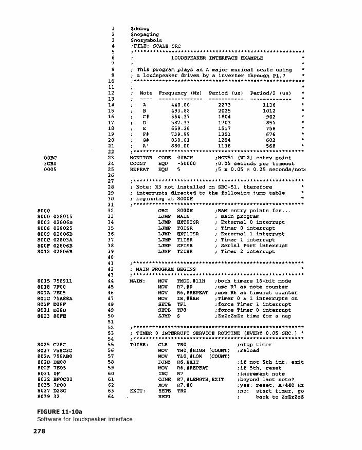
FIGURE 11-10a
Software for loudspeaker interface
278

DESIGN AND INTERFACE EXAMPLES | 279
FIGURE 11-10b
continued

280 | CHAPTER 11
FIGURE 11-11
Cover page for the X2444 nonvolatile RAM data sheet
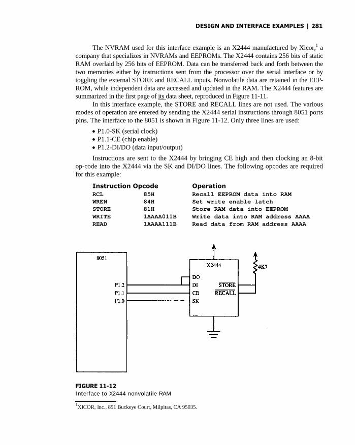
DESIGN AND INTERFACE EXAMPLES | 281
The NVRAM used for this interface example is an X2444 manufactured by Xicor,1 acompany that specializes in NVRAMs and EEPROMs. The X2444 contains 256 bits of staticRAM overlaid by 256 bits of EEPROM. Data can be transferred back and forth between thetwo memories either by instructions sent from the processor over the serial interface or bytoggling the external STORE and RECALL inputs. Nonvolatile data are retained in the EEP-ROM, while independent data are accessed and updated in the RAM. The X2444 features aresummarized in the first page of its data sheet, reproduced in Figure 11-11.
In this interface example, the STORE and RECALL lines are not used. The variousmodes of operation are entered by sending the X2444 serial instructions through 8051 portspins. The interface to the 8051 is shown in Figure 11-12. Only three lines are used:
P1.0-SK (serial clock) P1.1-CE (chip enable) P1.2-DI/DO (data input/output)
Instructions are sent to the X2444 by bringing CE high and then clocking an 8-bitop-code into the X2444 via the SK and DI/DO lines. The following opcodes are requiredfor this example:
Instruction Opcode Operation
RCL 85H Recall EEPROM data into RAMWREN 84H Set write enable latchSTORE 81H Store RAM data into EEPROMWRITE 1AAAA011B Write data into RAM address AAAAREAD 1AAAA111B Read data from RAM address AAAA
FIGURE 11-12
Interface to X2444 nonvolatile RAM
1XICOR, Inc., 851 Buckeye Court, Milpitas, CA 95035.

282 | CHAPTER 11
EXAMPLE Design Objective
11.5 Write the following two programs. The first, called SAVE, copies the contents of 8051internal locations 60H-7FH to the X2444 EEPROM. The second, called RECOVER,reads previously saved data from the X2444 EEPROM and restores it to locations60H-7FH. These are two distinct programs. Typically the SAVE program is executedwhen ever nonvolatile information is changed (for example, by a user altering aconfiguration parameter). The RECOVER program is executed each time the system ispowered up or reset. For this example, the nonvolatile information is kept in the 8051internal locations 60H-7FH (presumably for access by a control program executing infirmware). The software listing is shown in Figure 11-13.
The operations of saving and recovering data involve the following steps:
Write Data into the X2444
1. Execute RCL (recall) instruction.2. Execute WREN (set write enable latch) instruction.3. Write data into X2444 RAN.4. Execute STO (store RAM into EEPROM) instruction.
5. Execute SLEEP instruction.
Read Data from X2444
1. Execute RCL (recall) instruction.2. Read data from X2444 RAM.
3. Execute SLEEP instruction.
As an example of what the software drivers must do, Figure 11-14 illustrates the timingdiagram to send the RCL instruction to the X2444. Several of the bits are actually "don'tcares" (as specified in the data sheet); however, they are shown as 0s in the figure.
The timing for the WRITE data and READ data instructions is slightly different.For these, the 8-bit opcode is followed immediately by 16 bits of data, and chip enableremains high for all 24 bits. For the read instruction, the eight bits (the opcode) are writtento the X2444, then 16 data bits are read from the X2444. Separate subroutines are used forreading eight bits (R_BYTE; lines 106-112) and writing eight bits (W_BYTE; lines 117-123). For specific details, consult the software listing.
11.8 INPUT/OUTPUT EXPANSION
The 8051 has four input/output ports, Port 0 to Port 3. If external memory is used, then all orpart of Port 0 and Port 2 would be taken up as data and/or address lines, thereby reducing thenumber of available I/O lines for general purpose I/O usage. In this section, we will discusstwo simple ways to increase the number of I/O lines. This is called expanding the I/O.
11.8.1 Using Shift Registers
Our next example illustrates a simple way to increase the number of input lines on the8051. Three port lines are used to interface to multiple (in this example, 2) 74HC165parallel-in serial-out shift registers. (See Figure 11-15.) The additional inputs are sampled

FIGURE 11-13a
Software for X2444 interface
283

284 | CHAPTER 11
FIGURE 11-13bcontinued

DESIGN AND INTERFACE EXAMPLES | 285
FIGURE 11-14Timing for the X2444 recall instruction
periodically by pulsing the SHIFT/LOAD line low. The data are then read into the 8051by reading the DATA IN line and pulsing the CLOCK line. Each pulse on the clock lineshifts the data ("down," as shown in Figure 11-15), so the next read to DATA IN reads thenext bit, and so on.
EXAMPLE Design Objective
11.6 Write a subroutine that copies the state of the 16 inputs in Figure 11-15 to 8051 internalRAM locations 25H and 26H.
The software to accomplish this is shown in Figure 11-16. Note that the main pro-gram loop consists of calls to two subroutines: GET_BYTES and DISPLAY_RESULTS(lines 34-35). The latter subroutine is included to illustrate a useful technique for debug-ging when resources are limited. DISPLAY_RESULTS (lines 72-83) reads the data frominternal locations 25H and 26H and sends each nibble to the console as a hexadecimalcharacter. This provides a simple visual interface to verify if the program and interface areworking. As input lines are toggled high and low, changes will immediately appear on theconsole (if the interface and program are working properly).
The GET_BYTES subroutine (lines 44-58) takes 112 µs to execute when two74HC165s are used and the system operates from a 12 MHz crystal. If the inputs weresampled, for example, 20 times per second, GET_BYTES would consume 112 ÷ 50,000 =0.2% of the CPU's execution time. This would have a minimal impact on the system's re-sources; however, increasing the number of input lines and/or the sampling rate may start toimpact overall system performance. Consult the software listing for further details.
11.8.2 Using the 8255
The 8255 is a programmable peripheral interface (PPI) IC that can be used to expand the805l's I/O. The 8255 is a 40-pin IC chip with three 8-bit ports known as Port A, Port B,and Port C. There are also two active-low input control signals, RD and WR, used toconnect to their 8051 counterparts. Meanwhile, pins D0 to D7 are the data pins used toconnect to the data bus of the 8051.
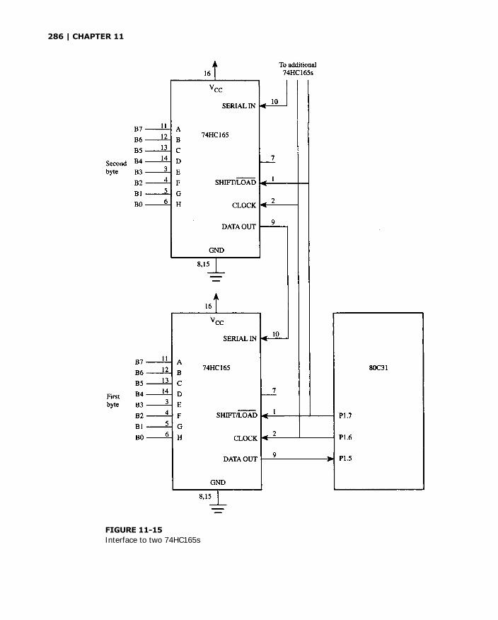
286 | CHAPTER 11
FIGURE 11-15
Interface to two 74HC165s

FIGURE 11-16a
Software for 75HC165 interface
287

288 | CHAPTER 11
FIGURE 11-16b
continued
Two input control pins. A0 and Al, are used to select specific ports within the 8255(See Table 11-2.) However, note that if both A0 and Al are set, this does not select a portbut instead selects the control register. The control register is an 8-bit register (See Table11-3) within the 8255 that is used to specify the mode of operation for all the three ports.This is similar to the 805l's TMOD and SCON registers, which are used to set theoperating modes of its timers and serial port, respectively.
The 8255 ports can be directed to operate in any one of four modes, but here we will justuse the simplest mode, mode 0 (Basic I/0). This mode sets the ports to provide simple input andoutput operations similar to the normal 8051 ports 0 to 3. Other more complex modes allow forhandshaking, which basically allows two devices (in this case the 8051 and the I/O device) tocommunicate more intelligently with each other through a series of handshaking signals.
TABLE 11-2
8255 port selection
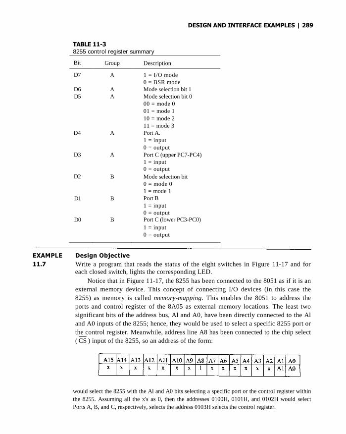
DESIGN AND INTERFACE EXAMPLES | 289
TABLE 11-38255 control register summary
Bit Group Description
D7 A 1 = I/O mode0 = BSR mode
D6 A Mode selection bit 1D5 A Mode selection bit 0
00 = mode 001 = mode 1
10 = mode 211 = mode 3
D4 A Port A.1 = input0 = output
D3 A Port C (upper PC7-PC4)1 = input0 = output
D2 B Mode selection bit0 = mode 01 = mode 1
D1 B Port B1 = input0 = output
D0 B Port C (lower PC3-PC0)
1 = input0 = output
EXAMPLE Design Objective
11.7 Write a program that reads the status of the eight switches in Figure 11-17 and foreach closed switch, lights the corresponding LED.
Notice that in Figure 11-17, the 8255 has been connected to the 8051 as if it is an
external memory device. This concept of connecting I/O devices (in this case the
8255) as memory is called memory-mapping. This enables the 8051 to address the
ports and control register of the 8A05 as external memory locations. The least two
significant bits of the address bus, Al and A0, have been directly connected to the Al
and A0 inputs of the 8255; hence, they would be used to select a specific 8255 port or
the control register. Meanwhile, address line A8 has been connected to the chip select
( CS ) input of the 8255, so an address of the form:
would select the 8255 with the Al and A0 bits selecting a specific port or the control register within
the 8255. Assuming all the x's as 0, then the addresses 0100H, 0101H, and 0102H would select
Ports A, B, and C, respectively, selects the address 0103H selects the control register.
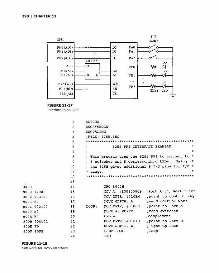
290 | CHAPTER 11
FIGURE 11-17
Interface to an 8255
FIGURE 11-18
Software for 8255 interface

DESIGN AND INTERFACE EXAMPLES | 291
This is a very simple interface example, and the software to do this is given in Figure11-18. The first step is to select the control register in order to set the mode of operation to 0.This is followed by sending out the appropriate control word to initialize Port A as input andPort B as output. Observe that the switches connected to Port A are in direct correspondenceto the LEDs connected to Port B. For example, a closed switch at pin 0 of Port A would give alow, signaling that we should light the corresponding LED at pin 0 of Port B by sending ahigh to that pin. Hence, Port A is first selected and its contents read into the accumulator,indicating the current status of the switches. Then, all we need to do is to complement thecontents of the accumulator, select Port B, and send the contents of the accumulator out to it.
11.9 RS232 (EIA-232) SERIAL INTERFACE
We have learn that the 8051 consists of a built-in serial port for interfacing to serial I/O de-vices. In fact, we could also connect the 8051 to the serial port of a personal computer (PC).The PC's serial port follows the RS232 or EIA-232 serial interface standard and for this rea-son, a normal RS232 cable can be used to connect between a PC and the 8051. The RS232cable is terminated at both ends by a connector (called DB-25) with 25 pins. However, sincenot all of these pins are used in most PC applications, there is also a different connector ver-sion called the DB-9 with only nine more commonly used pins. Whether it is DB-25 or DB-9,the three most important pins are the receive data (RXD), transmit data (TXD), and ground(GND). The RS232 serial interface also allows for handshaking, where in order to establish acommunications channel, one device initiates by sending the request to send (RTS) signal toanother device and waits for the corresponding clear to send (CTS) signal to be returned.Upon reception of CTS, the two devices can then communicate messages back and forth.
When connecting the 8051 to the RS232 serial interface, one major concern is thedifference in voltage levels between them. The 8051 uses the TTL voltage levels where a5V would indicate a high while a DV indicates a low. Meanwhile, for the RS232, a high isdefined as being +3V to +15V while a low is between -5V to -15V. Because of thisdifference, connections between the 8051 and the RS232 have to be done through linedrivers. Line drivers basically function to convert between the two different voltage levelsso that a high or low as understood by the 8051 also means a high or low to the RS232 andvice versa. Figure 11-19 shows how the 8051 is connected to the RS232 serial interface viaRS232 line drivers such as the 1488/1489.
FIGURE 11-19Interface to RS232

292 | CHAPTER 11
EXAMPLE Design Objective11.8 The 8051 is connected to the PC through the RS232 serial interface. Write a program that
inputs decimal numbers from the PC attached to the 8051 serial port, and sends the corre-sponding ASCII code out to the screen.
The software for this is shown in Figure 11-20. First, the FACE subroutine iscalled for initializing the serial port and to perform the handshaking with the serial in-terface before an initial message is transmitted. For this purpose, the serial port is setfor mode 1, 8-bit UART and the corresponding baud rate to 9600 baud. The RTSsignal is then asserted and the 8051 waits for the acknowledging CTS signal from theserial interface. Only when CTS is detected will an initial message be sent out throughthe serial port.
FIGURE 11-20a
Software for RS232 interface
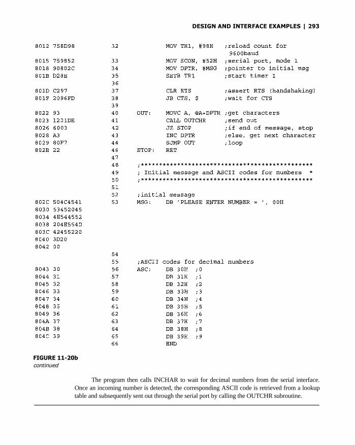
DESIGN AND INTERFACE EXAMPLES | 293
FIGURE 11-20b
continued
The program then calls INCHAR to wait for decimal numbers from the serial interface.
Once an incoming number is detected, the corresponding ASCII code is retrieved from a lookuptable and subsequently sent out through the serial port by calling the OUTCHR subroutine.
294 | CHAPTER 11
TABLE 11-4DB-25 Centronics parallel interface pins
11.10 CENTRONICS PARALLEL INTERFACE
The most common printer interface is the Centronics parallel interface. This has becomethe de facto standard for parallel interface, just like its RS232 counterpart in the previoussection. The Centronics parallel interface specifies 36 signals. This interface can either beterminated by a 36-pin Centronics connector, or even a DB-25 connector, as is more com-mon on most PCs nowadays. (See Table 11-4.) In this section, we will see how to connectthe 8051 to a printer through the DB-25 Centronics parallel interface.
The Centronics parallel interface consists of eight data pins to carry a byte of data for
printing. When a byte of data has been made available at these data pins, the 8051 sends a
STROBE signal that allows the 8051 to inform the printer that data is available at its data
pins. If the printer is not busy, it would send a corresponding ACK signal to indicate that it
has successfully processed the print request. Otherwise, a BUSY signal would be sent instead.
EXAMPLE Design Objective
11.9 Write a program to query the printer and then continually send a test message to it for printing.
Figure 11-21 shows the connection of the 8051 to a printer via the Centronics parallel
interface. The corresponding software is given in Figure 11-22. The program first activates the
STROBE signal to the printer and then checks the status of the printer to ensure that it is not
busy (BUSY = 0), that there is still paper (PAPER END = 0), that it has been selected (SLOT
= 1), and that there is no error ( ERROR = 1). If any of the conditions are

FIGURE 11-21
Interface to Centronics parallel interface
FIGURE 11-22a
Software for Centronics parallel interface
295
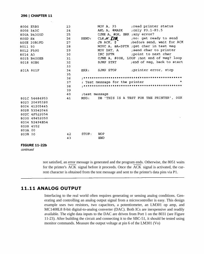
296 | CHAPTER 11
FIGURE 11-22b
continued
not satisfied, an error message is generated and the program ends. Otherwise, the 8051 waits
for the printer's ACK signal before it proceeds. Once the ACK signal is activated, the cur-
rent character is obtained from the test message and sent to the printer's data pins via P1.
11.11 ANALOG OUTPUT
Interfacing to the real world often requires generating or sensing analog conditions. Gen-erating and controlling an analog output signal from a microcontroller is easy. This designexample uses two resistors, two capacitors, a potentiometer, an LM301 op amp, andMC1408L8 8-bit digital-to-analog converter (DAC). Both ICs are inexpensive and readilyavailable. The eight data inputs to the DAC are driven from Port 1 on the 8031 (see Figure11-23). After building the circuit and connecting it to the SBC-51, it should be tested usingmonitor commands. Measure the output voltage at pin 6 of the LM301 (Vo)

DESIGN AND INTERFACE EXAMPLES | 297
while writing different values to Port 1 and adjusting the 1K potentiometer. The outputshould vary from 0 volts (P1 = 00H) to about 10 volts (P1 = 0FFH).
Once the circuit is operating correctly, we are ready to have fun with the interfacesoftware. The usual test program is a sawtooth waveform generator that sends a value tothe DAC, increments the value, sends it again, and so on (see question 3 at the end of thischapter). However, we will embark on a much more ambitious design—a digitallycontrolled sine wave generator.
EXAMPLE Design Objective11.10 Write a program to generate a sine wave using the DAC interface in Figure 11-23. Use a
constant call STEP to set the frequency of the sine wave. Make the program interruptdriven with an update rate of 10 kHz.
Since the number-crunching capabilities of the 8031 are very limited, the only rea-sonable approach to this problem is to use a look-up table. We need a table with 8-bitvalues corresponding to one period of a sine wave. The values should start around 127,increase to 255, decrease through 127 to D, and rise back up to 127, following the patternof a sine wave.
A reasonable rendition of a sine wave requires a relatively large table; so the ques-tion arises, how do we generate the table? Manual methods are impractical. The easiest
FIGURE 11-23Interface to MC1408L8
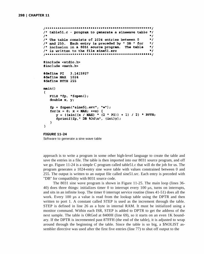
298 | CHAPTER 11
FIGURE 11-24
Software to generate a sine wave table
approach is to write a program in some other high-level language to create the table andsave the entries in a file. The table is then imported into our 8031 source program, and offwe go. Figure 11-24 is a simple C program called table51.c that will do the job for us. Theprogram generates a 1024-entry sine wave table with values constrained between 0 and255. The output is written to an output file called sine51.src. Each entry is preceded with"DB" for compatibility with 8031 source code.
The 8031 sine wave program is shown in Figure 11-25. The main loop (lines 36-40) does three things: initializes timer 0 to interrupt every 100 s, turns on interrupts,and sits in an infinite loop. The timer 0 interrupt service routine (lines 41-51) does all thework. Every 100 µs a value is read from the lookup table using the DPTR and thenwritten to port 1. A constant called STEP is used as the increment through the table.STEP is defined in line 26 as a byte in internal RAM. It must be initialized using amonitor command. Within each ISR, STEP is added to DPTR to get the address of thenext sample. The table is ORGed at 8400H (line 69), so it starts on an even 1K bound-ary. If the DPTR is incremented past 87FFH (the end of the table), it is adjusted to wraparound through the beginning of the table. Since the table is so big, a $NOLIST as-sembler directive was used after the first five entries (line 77) to shut off output to the

FIGURE 11-25a
8031 Sine wave program
299

300 | CHAPTER 11
FIGURE 11-25b
continued
listing file. A $LIST directive was used in line 1092 (not shown) to turn the listingback on for the last five entries. The frequency of the sine wave is controlled by threeparameters: STEP, the size of the table, and the timer interrupt period, as explained inlines 16-20 of the listing.
11.12 ANALOG INPUT
Our next design example is an analog input channel. The circuit in Figure 11-26 uses oneresistor, one capacitor, a trimpot, and an ADC0804 analog-to-digital converter (ADC). TheADC0804 is an inexpensive ADC (National Semiconductor Corp.) that converts an inputvoltage to an 8-bit digital word in about 100 µs.
The ADC0804 is controlled by a write input ( WR ) and an interrupt output ( INTR )
A conversion is started by pulsing WR low. When the conversion is complete (100 ms
later), the ADC0804 asserts INTR , making it low. INTR is de-asserted (high) on the
next 1-to-0 transition of WR, which initiates the next conversion. INTR and WR connect
to the 8031 lines P1.1 and P1.0, respectively. For this example, we use Port A of the 8155
for the data transfer, as shown in the figure.The ADC0804 operates from an internal clock created by the RC network con-
necting to pins 19 and 4. The analog input voltage is a differential signal applied to theVin( + ) and Vin( - ) inputs on pins 6 and 7. For this example Vin( - ) is grounded and Vin(+ ) is driven from the center tap of the trimpot. Vin(+ ) will range from 0 to +5 volts, ascontrolled by the trimpot. Consult the data sheet for a detailed description of the operationof the ADC0804.

DESIGN AND INTERFACE EXAMPLES | 301
FIGURE 11-26Interface to ADC0804 ADC
EXAMPLE Design Objective
11.11 Write a program to continually sense the voltage at the trimpot's center tap (as convertedby the ADC0804). Report the result on the console as an ASCII byte.
The program in Figure 11-27 achieves the objective stated above. Since the 8155
ports default to input upon reset, an initialize sequence is not necessary. Port A is at
address 0101H in external memory and is easily read using a MOVX instruction. A
conversion is started by clearing and setting P1.0 (lines 34-35), the ADC0804's WR
input. Then, the program sits in a loop waiting for the ADC0804 to finish the conversion
and assert INTR at P1.1 (line 36). The data are read in lines 37 and 38 and then sent to
the console, using MON51's OUT2HX subroutine (line 39). As the program runs, a byte is
displayed on the console. It will range from 00H to 0FFH as the trimpot is adjusted.The program in Figure 11-27 is a rough first approximation of the potential for ana-
log input. It is possible to replace the trimpot with other analog inputs. Temperature sens-ing is achieved using a thermistor—a device with a resistance that varies withtemperature. Speech input is possible using a microphone. The ADC80804's conversionperiod of 100 µs translates into a sampling frequency of 10 kHz. This is sufficient tocapture signals with up to 5 kHz bandwidth, roughly equivalent to a voice-gradetelephone line. Additional circuitry is required to boost the low-level signals provided bytypical microphones to the 0-5 volt range expected by the ADC0804. Additionally, asample-and-hold circuit is needed to maintain a constant voltage for the duration of eachconversion. We'll leave it to the reader to explore these possibilities.

FIGURE 11-27
Software for ADC0804 interface
302

DESIGN AND INTERFACE EXAMPLES | 303
11.13 INTERFACE TO SENSORS
In Chapter 6's section on external interrupts, an example was given on the furnace controller thatmakes use of a simple temperature sensor. In this section, we will look at a more complextemperature sensor, the DS1620 digital thermometer and thermostat, manufactured by Maxim.2
The DS1620 is an 8-pin IC with three thermal alarm outputs, THIGH, TLOW, and TCOM.THIGH goes high if the measured temperature is greater than or equal to the user-defined hightemperature, TH. On the other hand, TLOW goes high if the temperature is less than or equal tothe user-defined low temperature, TL. In contrast, TCOM goes high when the temperatureexceeds TH and only returns low when the temperature is less than TL.
To use the DS1620 along with the 8051, the DS1620 has to be configured for 3-wirecommunications. This is so called due to the fact that the communication between them isdone through a group of three wires, namely the data input/output (DQ) pin, the clock input(CLK/CONV) pin, and the reset input (RST) pin. Communication is initiated by setting theRST, and as clock signals are sent to the DS1620 through the CLK pin, data would beclocked in or out through the DQ pin, with the LSB sent first.
Figure 11-28 shows the connections between the 8051 and the DS1620. Interactingwith the DS1620 requires the 8051 to issue commands (see Table 11-5) to it.
FIGURE 11-28Interface to DS1620
TABLE 11-5DS1620 command set
2Maxim Integrated Products, Inc., 120 San Gabriel Drive, Sunnyvale, CA 94086.
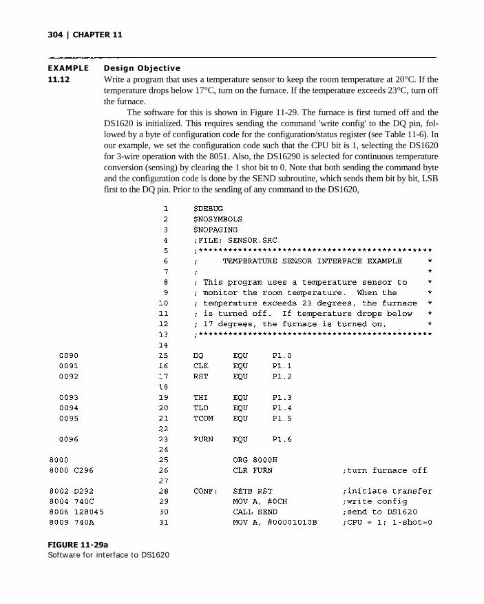
304 | CHAPTER 11
EXAMPLE Design Objective
11.12 Write a program that uses a temperature sensor to keep the room temperature at 20°C. If thetemperature drops below 17°C, turn on the furnace. If the temperature exceeds 23°C, turn offthe furnace.
The software for this is shown in Figure 11-29. The furnace is first turned off and theDS1620 is initialized. This requires sending the command 'write config' to the DQ pin, fol-lowed by a byte of configuration code for the configuration/status register (see Table 11-6). Inour example, we set the configuration code such that the CPU bit is 1, selecting the DS1620for 3-wire operation with the 8051. Also, the DS16290 is selected for continuous temperatureconversion (sensing) by clearing the 1 shot bit to 0. Note that both sending the command byteand the configuration code is done by the SEND subroutine, which sends them bit by bit, LSBfirst to the DQ pin. Prior to the sending of any command to the DS1620,
FIGURE 11-29a
Software for interface to DS1620

DESIGN AND INTERFACE EXAMPLES | 305
FIGURE 11-29bcontinued

306 | CHAPTER 11
TABLE 11-6DS1620 configuration/status register
transfer has to be initiated by raising RST to high. When the command has been sent, thetransfer is stopped by clearing RST.
After the 'write config' command, the user-defined high temperature, TH, and the user-defined low temperature, TL, is set. Next, a 'start convert' command is issued to direct theDS1620 to start sensing the temperature. The 8051 then waits in an indefinite loop on thestatus of the THIGH and TLOW outputs and turns the furnace on or off correspondingly.
11.14 INTERFACE TO RELAYS
A relay is a switch whose contacts are opened or closed due to a magnetic field produced bythe application of electricity to it. In essence, relays can be thought of as magneto-mechanical
FIGURE 11-30Internal connections for G6RN
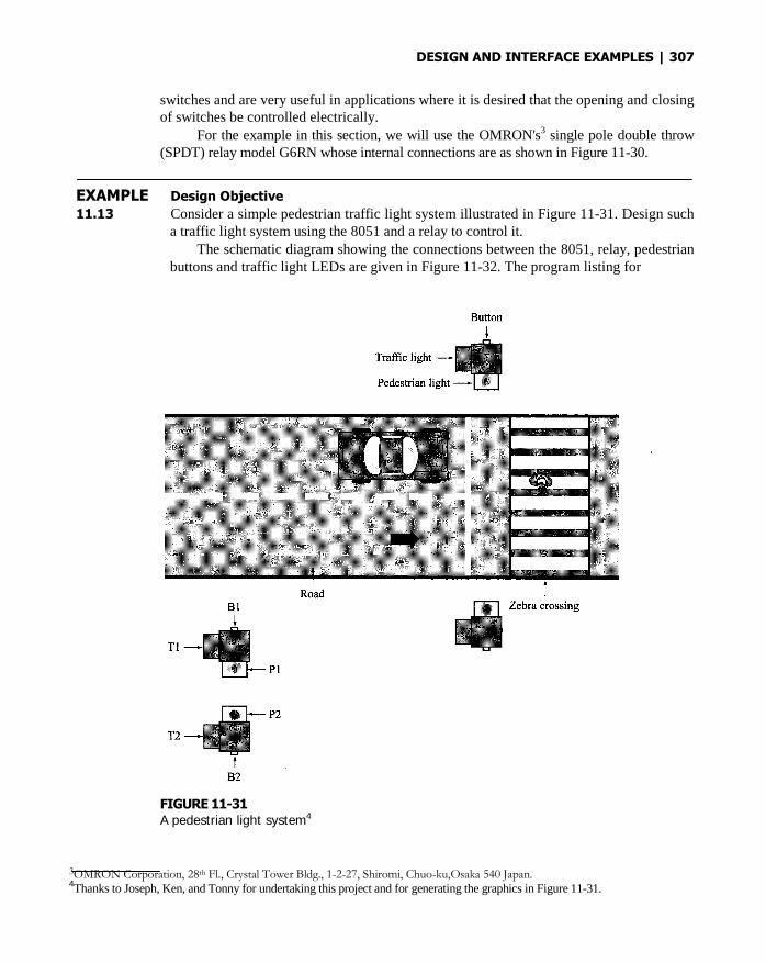
DESIGN AND INTERFACE EXAMPLES | 307
switches and are very useful in applications where it is desired that the opening and closingof switches be controlled electrically.
For the example in this section, we will use the OMRON's3 single pole double throw(SPDT) relay model G6RN whose internal connections are as shown in Figure 11-30.
EXAMPLE Design Objective
11.13 Consider a simple pedestrian traffic light system illustrated in Figure 11-31. Design sucha traffic light system using the 8051 and a relay to control it.
The schematic diagram showing the connections between the 8051, relay, pedestrianbuttons and traffic light LEDs are given in Figure 11-32. The program listing for
FIGURE 11-31A pedestrian light system4
3OMRON Corporation, 28th Fl., Crystal Tower Bldg., 1-2-27, Shiromi, Chuo-ku,Osaka 540 Japan.4Thanks to Joseph, Ken, and Tonny for undertaking this project and for generating the graphics in Figure 11-31.

308 | CHAPTER 11
FIGURE 11-32Interface to G6RN: Pedestrian Light System
the corresponding software is in Figure 11-33. The main program enables the relevantinterrupts and waits until a pedestrian pushes a button (B1 or B2 depending on which sideof the road he or she is on). Initially, port 1.0 is LOW, and the pole within the relay causesthe GREEN traffic light and RED pedestrian light to be on. Once a button is pressed, thisgenerates an interrupt INT0 to the 8051, which calls the corresponding interrupt serviceroutine EX0ISR, the main bulk of the program. Within this ISR, port 1.0 is set, causing
FIGURE 11-33a
Software for interface to the G6RN

DESIGN AND INTERFACE EXAMPLES | 309
FIGURE 11-33b
continued
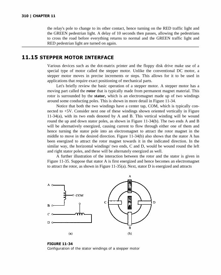
310 | CHAPTER 11
the relay's pole to change to its other contact, hence turning on the RED traffic light andthe GREEN pedestrian light. A delay of 10 seconds then passes, allowing the pedestriansto cross the road before everything returns to normal and the GREEN traffic light andRED pedestrian light are turned on again.
11.15 STEPPER MOTOR INTERFACE
Various devices such as the dot-matrix printer and the floppy disk drive make use of aspecial type of motor called the stepper motor. Unlike the conventional DC motor, astepper motor moves in precise increments or steps. This allows for it to be used inapplications that require exact positioning of mechanical parts.
Let's briefly review the basic operation of a stepper motor. A stepper motor has amoving part called the rotor that is typically made from permanent magnet material. Thisrotor is surrounded by the stator, which is an electromagnet made up of two windingsaround some conducting poles. This is shown in more detail in Figure 11-34.
Notice that both the two windings have a center tap, COM, which is typically con-nected to +5V. Consider next one of these windings shown oriented vertically in Figure11-34(a), with its two ends denoted by A and B. This vertical winding will be woundround the up and down stator poles, as shown in Figure 11-34(b). The two ends A and Bwill be alternatively energized, causing current to flow through either one of them andhence turning the stator pole into an electromagnet to attract the rotor magnet in themiddle to move in the desired direction. Figure 11-34(b) also shows that the stator A hasbeen energized to attract the rotor magnet towards it in the indicated direction. In thesimilar way, the horizontal windings' two ends, C and D, would be wound round the leftand right stator poles, and these will be alternately energized as well.
A further illustration of the interaction between the rotor and the stator is given inFigure 11-35. Suppose that stator A is first energized and hence becomes an electromagnetto attract the rotor, as shown in Figure 11-35(a). Next, stator D is energized and attracts
FIGURE 11-34
Configuration of the stator windings of a stepper motor

DESIGN AND INTERFACE EXAMPLES | 311
FIGURE 11-35
Rotating the rotor of the stepper motor
the rotor towards it, as in Figure 11-35(b). This is followed by energizing stator B, againattracting the rotor as in Figure 11-35(c). Finally, stator C is energized and similarly at-tracts the rotor. The energizing of the stators in the sequence A, D, B, C causes the rotor torotate in clockwise direction to complete one revolution, or the rotor is said to have madea 360° clockwise rotation. In contrast, if the stators are energized in the opposite sequence,the rotor would make a counterclockwise rotation.
Notice that the rotor, when operated in this way, moves to four unique positions asit steps to one full rotation, where each step involves a rotation of 90°. A stepper motor ofsuch type is called a 4-step stepper motor. For finer resolutions, 8-step stepper motorscan be used, where a step makes a rotation of 45. This is achieved for example byenergizing the stator poles not only one at a time but alternatively energizing two adjacentstators at a time. For example, to rotate the stepper motor clockwise, we energize thestator poles according to the sequence A, AD, D, DB, B, BC, C, CA. The first three stepsare illustrated in Figure 11-36.
FIGURE 11-36
Half-step rotation of the stepper motor

312 | CHAPTER 11
The connection from the 8051 to the windings of the stepper motor has to be madethrough a stepper motor driver as the currents from the 8051 port pins are insufficient todrive the windings. Figure 11-37 shows how the ULN2003 stepper motor driver interfacesthe 8051 to the stepper motor.
With the connections in Figure 11-37, it is clear that to energize a stator pole, a high '1'has to be written to the corresponding port pin connected to it, allowing current to flow throughthe stator windings thus turning it into an electromagnet. The sequence of steps for both the 4-step and 8-step stepper motors are given in Table 11-7 and Table 11-8, respectively.
TABLE 11-7
Full-step 4-step sequence for clockwise rotation
TABLE 11-8Half-step 8-step sequence for clockwise rotation
FIGURE 11-37
Interface to the stepper
motor

DESIGN AND INTERFACE EXAMPLES | 313
EXAMPLE Design Objective11.14 Write a program to initially rotate the stepper motor clockwise. If a switch connected to
INT0 makes a high-to-low transition, change the direction of rotation, in this case it be-comes counterclockwise.
The software for this is shown in Figure 11-38. Since the external interrupt 0 ( INT0 )
is used to detect the high-to-low transition, a relevant ISR for INT0 is included as part of
FIGURE 11-38aSoftware for stepper motor interface

FIGURE 11-38b
continued
314

DESIGN AND INTERFACE EXAMPLES | 315
the program such that the direction bit, D, is complemented at every occurrence of a high-
to-low transition at INT0 . There are also two functions, CW and CCW, to cause the step-
per motor to rotate clockwise and anticlockwise, respectively, plus a simple subroutine
that generates a delay of 1 second.The main program initially directs the stepper motor to rotate in a clockwise fashion.
Upon completion of one cycle of rotation, the current direction is checked by referring toD, and then either CW or CCW would be called to continue rotating the stepper motor inthe direction indicated by D.
SUMMARY
This concludes our examination of interface examples. The designs presented illustrate manyof the concepts required to implement sophisticated interfaces using an 8051 microcontroller.
There is no substitute for hands-on experience, however. The examples in this chapter,and those presented earlier, are best understood through a trial-and-error process. Implement-ing the examples on a real system, such as the SBC-51, is the best way to develop the conceptspresented in this book. This book has provided a basis for students to explore further the pos-sibilities of using a microcontroller such as the 8051 in minimum component designs.
PROBLEMS
11.1 Use the loudspeaker interface in Figure 11-9 to repeatedly play the musical melodyshown in Figure 11-39.
11.2 Reconfigure the 74HC165 interface in Figure 11-15 and rewrite the accompanyingsoftware in Figure 11-16 to use the 8051's serial port (in mode 0) for the clock and datalines.
11.3 If the following program is used with the digital-to-analog output circuit in Figure 11-23, a sawtooth wave results. (Assume 12 MHz operation.)
STEP EQU 1
MAIN MOV P1,A
ADD A,#STEP
SJMP MAIN
FIGURE 11-39Musical melody for Problem 11.1
316 | CHAPTER 11
a. What is the frequency of the sawtooth wave?b. What value for STEP will achieve an output frequency of 10 kHz (approximately)?c. Derive the equation for frequency, given STEP.
11.4 Several of the programs in this chapter used MON51 subroutines. If a program isto use the subroutine ISDIG (to check if a byte is an ASCII digit), what addressfrom MON51 must be equated to the symbol ISDIG?
11.5 Write a program to create a 1 kHz square wave on P1.7 using the 8155 timer andexternal 0 interrupts. (Hint: consult an 8155 data sheet.)
11.6 Assume the 74HC165 interface in Figure 11-15 is expanded to 6 ICs, providing 48additional input lines.a. How should the program in Figure 11-16 be modified to read the 48 input lines?b. Where will the data be stored in the 8031's internal RAM?c. What is the new duration of the GET_BYTES subroutine in Figure 11-16?d. If GET_BYTES is placed in an interrupt service routine that executes every
second, what percentage of the CPU's execution time is spent reading the48 inputs from the 74HCl65s?
11.7 In Figure 11-25, the constant STEP was defined as a byte of internal data atlocation 50H using the following assembler directive:
STEP DATA 50H
This is the correct way to define STEP; however, the following would also work:
STEP EQU 50H
In the latter case, type-checking is not performed by ASM51 when the program isassembled. Give an example of an incorrect use of the label STEP that would notgenerate an assemble-time error if STEP were defined with EQU, but wouldgenerate an error if STEP were defined properly, using DATA.
11.8 Suppose a 16-key HEX keypad has been connected to the 8051 as shown in Figure11-40. The columns are numbered from left to right, starting from 0, while therows are numbered from up to down, also starting from 0. Suppose that when akey-press is detected, the HIT subroutine is called, and R6 contains the column in-formation and the upper 4 bits of P1 contain the row information, where
Write the subroutine HIT that uses the values in R6 and P1 to output the value of thekey pressed. Show your steps.

DESIGN AND INTERFACE EXAMPLES | 317
FIGURE 11-40
11.9 Rewrite
to the 80
11.10 We have8255 andthose mo
11.11 Comparedifferencand mode
11.12 Write the
11.13 Researchspecific e
HEX keypad
the software for the LCD in Figure 11-8 to continually display the message "Welcome
51 Microcontroller Experience. Hope you enjoy your reading adventure."
seen how to use the 8255 in mode 0. Research on the more complex modes of thehence write the assembly language instructions to initialize the 8255's ports to each of
des.
between the serial and parallel interface. What in your opinion is the most significante? Hence why do you think serial interfaces are commonly used with keyboards, mice,ms while parallel interfaces are used with printers?corresponding pseudo code for the pedestrian traffic light software in Figure 11-33.
the types and applications of stepper motors. Select three such applications and givexplanations as to why the stepper motor is used in each of them.

318 | CHAPTER 11
Write the subroutine HIT that uses the values in R6 and P1 to output the value of thekey pressed. Show your steps.

Design and InterfaceExamples in C
12.1 INTRODUCTION
In the previous chapter, several design and interface examples involving the 8051 werepresented, with the corresponding interface programs written in assembly language. Thischapter will tackle these interface problems by writing similar proof-of-concept programsin 8051 C. This will give a clearer view on the difference and also the similarities betweenthe two languages that we use to interact with the 8051.
12.2 HEXADECIMAL KEYPAD INTERFACE
Recall from the discussion of the previous chapter the hexadecimal keypad interfacewhere the design objective was to write a program to continually read hexadecimalcharacters from the 4 x 4 keypad and echo the corresponding ASCII code to the console. Asimilar 8051 C program is shown in Example 12.1.
EXAMPLE Hexadecimal Keypad Interface12.1 Rewrite in C language the software for the hexadecimal keypad interface in Figure 11-4.
Solution
#include <reg51.h>#include <stdio.h>
unsigned char R3, R5, R6, R7, tempA;unsigned char bdata A; /* represents ACC */sbit aMSB = A^7; /* variable aMSB to refer to
A.7 */
319
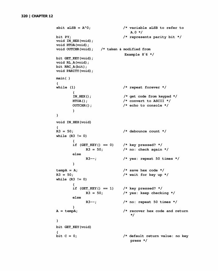
sbit aLSB = A^0; /* variable aLSB to refer toA.0 */
bit PY; /* represents parity bit */void IN_HEX(void);void HTOA(void);void OUTCHR(void); /* taken & modified from
Example 8-6 */bit GET_KEY(void);void RL_A(void);bit RRC_A(bit);void PARITY(void);
main( )
{while (1) /* repeat forever */
{IN_HEX(); /* get code from keypad */HTOA(); /* convert to ASCII */OUTCHR(); /* echo to console */
}}
void IN_HEX(void)
{R3 = 50; /* debounce count */
while (R3 != 0)
{if (GET_KEY() == 0) /* key pressed? */
R3 = 50; /* no: check again */
elseR3--; /* yes: repeat 50 times */
}
tempA = A; /* save hex code */R3 = 50; /* wait for key up */while (R3 != 0)
{if (GET_KEY() == 1) /* key pressed? */
R3 = 50; /* yes: keep checking */else
R3--; /* no: repeat 50 times */
}A = tempA; /* recover hex code and return
*/
}
bit GET_KEY(void)
{bit C = 0; /* default return value: no key
press */
320 | CHAPTER 12

DESIGN AND INTERFACE EXAMPLES IN C | 321
A = 0xFE; /* start with column 0 */
for (R6 = 4; R6 > 0; R6--) /* check all 4 columns */{P1 = A; /* activate column line
*/A = P1; /* read back Port 0 */tempA = A&(0xF0); /* isolate row lines */if (tempA == 0xF0) /* row lines active? */
RL_A(); /* no: move to nextcolumn line */
else{R7 = A; /* save in R6 */A = 4; /* prepare to calculate
col. weighting */C = 0;A = A - R6; /* 4 - R6 = weighting */R6 = A; /* save in R6 */A = R7; /* restore scan code */A = ( R7 << 4 | R7 >> 4 );/* put in low nibble */
for (R5 = 4; R5 > 0; R5--)/* use R5 as counter*/ {
C = RRC_A(C); /* rotate ACC until 0 */if (C == 0)
break; /* done when C = 0 */else
R6 = R6 + 4; /* add 4 until row found*/
}C = 1; /* key pressed! */A = R6; /* code in ACC */return C;}
}return C;}
void RL_A(void){bit tempBit;tempest = aMSB; /* backup MSB of A */A = A << 1; /* rotate A left */aLSB = tempBit;} /* rotate aLSB into MSB */
bit RRC_A(bit C)
{bit tempBit;
tempBit = C; /* backup C */

322 | CHAPTER 12C = aLSB; /* rotate A.0 into C */A = A >> 1; /* rotate A right */aMSB = tempBit; /* rotate C into A.7 */return C; }
void HTOA(void){A = A & 0xF; /* ensure upper nibble clear */if (A >= 0xA) /* 'A' to 'F'? */
A = A + 7; /* yes: add extra */A = A + '0'; /* no: convert directly */}
void OUTCHR(void){PARITY(); /* get even parity of A and put
in PY */PY = !PY; /* change to odd parity */aMSB = PY; /* add to character code */while (TI != 1); /* Tx empty? no: check again */TI = 0; /* yes: clear flag and */SBUF = A; /* send character */aMSB = 0; /* strip off parity bit */}
void PARITY(void){int i;PY = 0; /* initialize parity to 0 */for ( i = 0; i < 8 ; i++ ) /* calculate parity of A*/
PY ^= ( A >> i ) & 1;}
Discussion
Recall that registers R0 to R7 are used for storing parameters in C functions. For this rea-son, it is often not advisable to use these registers for temporary storage when programingthe 8051 in C. Instead, simply declare any 8-bit variable for this purpose. Notice also thatin our example above, we intentionally named the temporary variables with the registernames R3 to R7 so that it is easier to relate our C program to the assembly language coun-terpart in Figure 11-4.
Due to the same reason, the accumulator, ACC, is used in most operations and hence isoften overwritten with data, so should not be used in your C programs. In our above example,we used a temporary bit-addressable variable A to represent the accumulator.
Since we do not use the ACC but use a representative, A, instead, the parity of Awould not be automatically updated in the parity flag, P. Instead, we would need tocompute it on our own. Therefore, we slightly modified OTCHR() to include the callingof a function PARITY( ) that computes the parity of A and stores it in a bit, PY.

DESIGN AND INTERFACE EXAMPLES IN C | 323
In our solution, we also included two functions, RL_A( ) and RRC_A( ), whichbasically work in the same way as the assembly language instructions RL A and RRC A.
We had to do this in C since no such C statements or functions support rotations. In C,only shift operations (denoted by <<) are supported.
12.3 INTERFACE TO MULTIPLE 7-SEGMENT LEDS
In Chapter 11, an assembly language program to interface the 8051 to multiple 7-segmentLEDs was presented. Specifically, the program was to copy BCD digits stored in internalRAM locations 70H to 71H, and send them to the LED display 10 times per second usinginterrupts. What follows will be a rough outline of a possible program written in C. It isleft to the reader to fine-tune and adapt it according to his individual preferences.
EXAMPLE Interface to Multiple 7-Segment LEDs
12.2 Rewrite in C language the software for the multiple 7-segment LED interface in Figure 11-6.
Solution
#include <reg5l.h>#include <stdio.h>
unsigned char bdata A; /* represents ACC */
int xdata * idata DPTR; /* DPTR in idata, points toxdata */
sbit DIN = P1^0; /* MC14499 interface lines */sbit CLOCK = P1^6;sbit ENABLE = P1^5;sbit aLSB = A^0;sbit aMSB = A^0;
int xdata X8155 = 0x100; /* 8155 address */
int xdata TIMER = X8155 + 4; /* timer registers */int count = 4000; /* interrupts @ 2000 ps */unsigned char mode = 0x40; /* timer mode hits */
int digits, icount;unsigned char tempA;
void UPDATE(void);void OUT8(void);bit RLC_A(bit);
main( )
{DPTR = TIMER; /* initialize 8155 timer */A = 0xA0; /* low byte of count for 500 Hz
square wave */DPTR[TIMER] = A;TIMER++;
A = 0xF; /* high byte of count */DPTR[TIMER] = A;
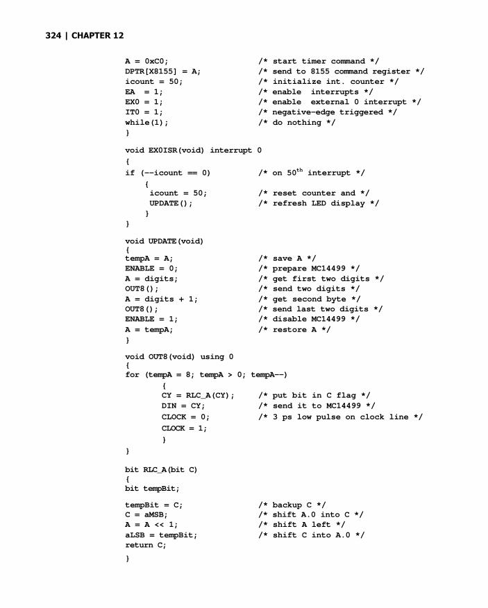
324 | CHAPTER 12
A = 0xC0; /* start timer command */DPTR[X8155] = A; /* send to 8155 command register */icount = 50; /* initialize int. counter */EA = 1; /* enable interrupts */EX0 = 1; /* enable external 0 interrupt */IT0 = 1; /* negative-edge triggered */
while(1); /* do nothing */}
void EX0ISR(void) interrupt 0
{
if (--icount == 0) /* on 50th interrupt */
{icount = 50; /* reset counter and */UPDATE(); /* refresh LED display */}
}
void UPDATE(void){tempA = A; /* save A */ENABLE = 0; /* prepare MC14499 */A = digits; /* get first two digits */OUT8(); /* send two digits */
A = digits + 1; /* get second byte */OUT8(); /* send last two digits */ENABLE = 1; /* disable MC14499 */
A = tempA; /* restore A */
}
void OUT8(void) using 0{for (tempA = 8; tempA > 0; tempA--)
{CY = RLC_A(CY); /* put bit in C flag */
DIN = CY; /* send it to MC14499 */
CLOCK = 0; /* 3 ps low pulse on clock line */
CLOCK = 1;
}
}
bit RLC_A(bit C){bit tempBit;
tempBit = C; /* backup C */C = aMSB; /* shift A.0 into C */A = A << 1; /* shift A left */
aLSB = tempBit; /* shift C into A.0 */return C;
}

DESIGN AND INTERFACE EXAMPLES IN C | 325
Discussion
In the 8051, the DPTR is used as a pointer to point to external memory locations. In orderto directly relate our C program to its assembly language counterpart, we use the declara-tion int xdata * idata DPTR to mean that the DPTR is a 16-bit pointer stored in idatamemory (where SFRs are located) which points to a location in xdata memory. In as-sembly language, elements in lookup tables are obtained by the instruction MOV @DPTP,A
or MOVC @DPTP,A, where the DPTR holds the base (starting) address of the table whileA is the index to a specific element. The situation is similar in C. A pointer, which we cancall DPTR, can be used to point to the Hirst element of an array (which is the C equivalentof a lookup table). Then, the statement DPTR[A] would refer to a specific element in thearray, where A is the index.
12.4 INTERFACE TO LIQUID CRYSTAL DISPLAYS (LCDS)
Section 11.5 presented an interface example involving an LCD. The program that waswritten continually retrieved ASCII characters from internal RAM locations 30H-7FH anddisplayed them on the LCD, 16 characters at a time. The same program, rewritten in C, isshown in Example 12.3.
EXAMPLE Interface to LCDs
12.3 Rewrite in C language the software for the LCD interface in Figure 11-8.
Solution
#include <reg51.h>#include <stdio.h>
sbit PS = P3^0;sbit RW = P3^1;sbit E = P3^2;sbit busy = P1^7;unsigned char bdata A; /* represents ACC */unsigned char * ptr;unsigned char count;void INIT(void);void NEW(void);void DISP(void);void WAIT(void);void OUT(void);
main( ){INIT(); /* initialize LCD */count = 16; /* initialize character count */while(1)
{for (ptr = 0x30; ptr < 0x80; ptr++, count--)}

326 | CHAPTER 12
A = *ptr; /* get next character */DISP(); /* display on LCD */if (count==0)
{count = 16; /* if end of line, reinitialize count */NEW(); /* and refresh LCD */}
}}
}
void INIT(void)
{A= 0x38; /* 2 lines, 5 X 7 matrix */WAIT(); /* wait for LCD to he free */RS = 0; /* output a command */OUT(); /* send it out */A = 0x0E; /* LCD on, cursor on */WAIT(); /* wait for LCD to he free */RS = 0; /* output a command */OUT(); /* send it out */NEW(); /* refresh LCD display */}
void NEW(void){A = 0x80; /* clear LCD */WAIT(); /* wait for LCD to he free */RS = 0; /* output a command */OUT(); /* send it out */
A = 0x80; /* cursor: line 1, position 1 */WAIT(); /* wait for LCD to he free */RS = 0; /* output a command */OUT(); /* send it out */}
void DISP(void){WAIT(); /* wait for LCD to be free */RS = 1; /* output a data */OUT(); /* send it out */}
void WAIT(void){do
{RS = 0; /* command */
RW = 1; /* read */busy = 1; /* make busy bit = input */

DESIGN AND INTERFACE EXAMPLES IN C | 327
E = 1; /* l-to-0 transition to */E = 0; /* enable LCD */}
while (busy); /* if busy, wait */
}
void OUT(void)
{
P1 = A; /* get ready output to LCD */RW = 0; /* write */
E = 1; /* l-to-0 transition to */E = 0; /* enable LCD */}
Discussion
In this example, we need to access some consecutive internal RAM locations. In assemblylanguage, this would be done via indirect addressing. In C, we make use of pointers andsince the pointed locations should be in internal RAM, our pointer, say ptr should be de-fined with the statement unsigned char data * ptr. We use unsigned char heresince memory locations contain 8-bit values. The rest of the program is straightforward.
12.5 LOUDSPEAKER INTERFACE
Recall that in Section 11.6 in the previous chapter, an interrupt-driven assembly languageprogram to continually play an A-major musical scale was presented. The followingExample 12.4 shows the corresponding program in C.
EXAMPLE Loudspeaker Interface
12.4 Rewrite in C language the software for the loudspeaker interface in Figure 11-10.
Solution
#include <reg51.h>#include <stdio.h>
#define LENGTH 12
sbit outbit = P1^7;
int reload; /* use this to temporarily store thereload */
/* value for the current note */int code * PC; /* PC points to the TABLE */int REPEAT = 5; /* reload value = -50000 causes 0.05
sec per */
/* timeout. Do 5 times, to get 5 x0.05 */
/* = 0.25 seconds per note */int ncount, tcount; /* note counter & timeout counter */
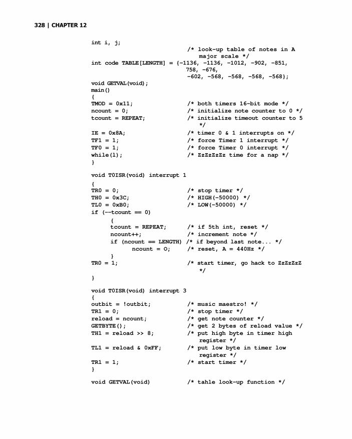
328 | CHAPTER 12
int i, j;/* look-up table of notes in A
major scale */int code TABLE[LENGTH] = {-1136, -1136, -1012, -902, -851,
758, -676,-602, -568, -568, -568, -568};
void GETVAL(void);main(){TMOD = 0x11; /* both timers 16-bit mode */ncount = 0; /* initialize note counter to 0 */tcount = REPEAT; /* initialize timeout counter to 5
*/
IE = 0x8A; /* timer 0 & 1 interrupts on */TF1 = 1; /* force Timer 1 interrupt */TF0 = 1; /* force Timer 0 interrupt */while(l); /* ZzZzZzZz time for a nap */}
void T0ISR(void) interrupt 1
{TR0 = 0; /* stop timer */TH0 = 0x3C; /* HIGH(-50000) */TL0 = 0xB0; /* LOW(-50000) */if (--tcount == 0)
{tcount = REPEAT; /* if 5th int, reset */ncount++; /* increment note */if (ncount == LENGTH) /* if beyond last note... */
ncount = O; /* reset, A = 440Hz */}
TR0 = 1; /* start timer, go hack to ZzZzZzZ
*/}
void T0ISR(void) interrupt 3{outbit = !outbit; /* music maestro! */TR1 = 0; /* stop timer */reload = ncount; /* get note counter */GETBYTE(); /* get 2 bytes of reload value */TH1 = reload >> 8; /* put high byte in timer high
register */TL1 = reload & 0xFF; /* put low byte in timer low
register */TR1 = 1; /* start timer */}
void GETVAL(void) /* tahle look-up function */

DESIGN AND INTERFACE EXAMPLES IN C | 329
{PC = TABLE; /* point to TABLE */reload = PC[reload]; /* read from TABLE into reload */
}
Discussion
The assembly language solution in Figure 11-10 uses a lookup table in code memory. To dothe same thing in C, we use an array that is stored in code memory. In our solution above,this array is called TABLE. The task of obtaining elements from this array is performed bya function GETVAL( ) that makes use of a pointer PC to access the array elements. Noticethat in contrast to the assembly language solution in Figure 11-10, we do not have to readfrom the table two times. This is because in C, you can define lookup tables with 16-bit el-ements to store each reload value as an element within it, as has been done in our exampleabove. Thus, we only read once from the table to get the 16-bit reload value. Then, we shiftit to the right by 8 bits to get its high byte, and simply mask off the higher 8 bits (by AND-ing them with 0) to get its low byte.
12.6 NONVOLATILE RAM INTERFACE
It was shown in Section 11.7 how a nonvolatile RAM (NVRAM) retains its contents evenduring the absence of power. An interface example was also given on how to copycontents from the 8051 to the NVRAM and to later read back the values stored. Theprogram in C is given by following Example 12.5.
EXAMPLE NVRAM Interface
12.5 Rewrite in C language, the software for the NVRAM interface in Figure 11-13.
Solution
#include <reg51.h>#include <reg5l.h>#include <stdio.h>#define RECALL 0x85 /* X2444 recall instruction */#define WRITE 0x84 /* X2444 write enable instruction */#define STORE 0x81 /* X2444 store instruction */#define SLEEP 0x82 /* X2444 sleep instruction */#define W_DATA 0x83 /* X2444 write data instruction */#define R_DATA 0x87 /* X2444 read data instruction */#define LENGTH 32 /* 32 hytes saved/restored */
unsigned char * R0; /* used to point to NVRAM locations */unsigned char R5, R6, R7;
unsigned char bdata A; /* represents accumulator */sbit aMSB = A^7; /* variahle aMSB to refer to A.7 */sbit aLSB = A^0; /* variable aLSB to refer to A.0 */sbit DIN = P1^2; /* X2444 interface lines */
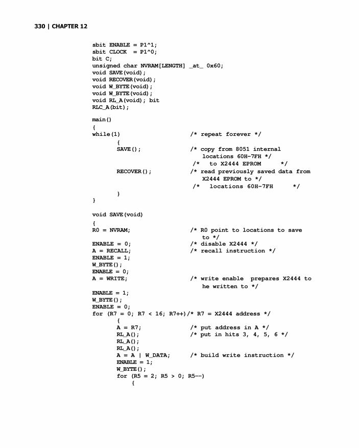
330 | CHAPTER 12
sbit ENABLE = P1^1;sbit CLOCK = P1^0;bit C;unsigned char NVRAM[LENGTH] _at_ 0x60;void SAVE(void);void RECOVER(void);void W_BYTE(void);void W_BYTE(void);void RL_A(void); bitRLC_A(bit);
main()
{while(1) /* repeat forever */
{SAVE(); /* copy from 8051 internal
locations 60H-7FH *//* to X2444 EPROM */
RECOVER(); /* read previously saved data fromX2444 EPROM to */
/* locations 60H-7FH */}
}
void SAVE(void)
{R0 = NVRAM; /* R0 point to locations to save
to */ENABLE = 0; /* disable X2444 */A = RECALL; /* recall instruction */ENABLE = 1;W_BYTE();ENABLE = 0;A = WRITE; /* write enable prepares X2444 to
he written to */ENABLE = 1;W_BYTE();ENABLE = 0;for (R7 = 0; R7 < 16; R7++)/* R7 = X2444 address */
{A = R7; /* put address in A */RL_A(); /* put in hits 3, 4, 5, 6 */RL_A();RL_A();A = A | W_DATA; /* build write instruction */ENABLE = 1;W_BYTE();for (R5 = 2; R5 > 0; R5--)
{

DESIGN AND INTERFACE EXAMPLES IN C | 331
A = *R0; /* get 8051 data */R0++; /* point to next byte */W_BYTE(); /* send byte to X2444 */}
ENABLE = 0;}A = STORE; /* if finished, copy to EPROM */ENABLE = 1;W_BYTE();ENABLE = 0;A = SLEEP; /* put X2444 to sleep */ENABLE = 1;W_BYTE();ENABLE = 0;}
void RECOVER(void)
{R0 = NVRAN;ENABLE = 0;A = RECALL; /* recall instruction */ENABLE = 1;W_BYTE();ENABLE = 0;for (R7 = 0; R7 < 16; R7++)/* R7 = X2444 address */
{A = R7; /* put address in A */RL_A(); /* build read instruction */RL_A();RL_A();A = A | R_DATA;ENABLE = 1;W_BYTE(); /* send read instruction
*/for (R5 = 2; R5 > 0; R5--)
{R_BYTE(); /* read byte of data */*R0 = A; /* put in 8051 RAM */R0++; /* point to next location */}
ENABLE = 0;}A = SLEEP; /* put X2444 to sleep */ENABLE = 1;R_BYTE();ENABLE = 0;}
void R_BYTE(void){for (R6 = 8; R6 > 0; R6--) /* use R6 as bit counter */

332 | CHAPTER 12
{C = DIN; /* put X2444 data bit in C */C = RLC_A(C); /* build byte in Accumulator */CLOCK = 1; /* toggle clock line (l us) */CLOCK = 0;}
}
void W_BYTE(void){for (R6 = 8; R6 > 0; R6--) /* use R6 as bit counter */
{C = RLC_A(C); /* put bit to write in C */DIN = C; /* put in X2444 DATA IN line */CLOCK = 1; /* clock bit into X2444 */CLOCK = 0;}
}
void RL_A(void)
{bit tempBit;
tempBit = aMSB; /* backup MSB of A */A = A << 1; /* rotate A left */aLSB = tempBit; /* rotate LSB into MSB */}
bit RLC_A(bit C){bit tempBit;
tempBit = C; /* backup C */C = aMSB; /* shift ACC.7 into C */A = A << 1; /* shift ACC left */aLSB = tempBit; /* shift C into ACC.0 */return C;}
DiscussionThis program requires that 32 bytes be allocated in internal data memory locations from 60H-7FH. This is achieved by declaring an array, NVRAM of 32 byte elements, and specifying thatit should start at absolute address 60H. The main program continually performs the saving ofdata bytes from internal data locations 60H-7FH to the NVRAM, and the restoring ofpreviously saved data from the NVRAM to the internal data locations 60H-7FH. Elements areread from the NVRAM array indirectly by way of a pointer, R0. Data are sent serially to andfrom the NVRAM, and the functions W_BYTE ( ) and R_BYTE ( ) are respectively used forthat purpose.

DESIGN AND INTERFACE EXAMPLES IN C | 333
12.7 INPUT/OUTPUT EXPANSION
In the previous chapter, two ways to expand the I/O were demonstrated in assembly lang-uage. The following two examples show how the same thing can be done in C. In par-ticular, Example 12.6 shows the method of I/O expansion by using shift registers, whileExample 12.7 shows how to expand the I/O by using the 8255.
EXAMPLE Interface to Shift Registers
12.6 Rewrite in C language the software for the Shift Register interface in Figure 11-16.
Solution
#include <reg51.h>#define COUNT 2 /* numher of shift registers */unsigned char bdata * R0;
unsigned char R6, R7;
unsigned char xdata * idata DPTR; /* DPTR in data, points to xdata */unsigned char bdata A; /* represents ACC */sbit aMSB = A^7;sbit aLSB = A^0;
sbit SHIFT = P1^7; /* SHIFT/LOAD input: 1 = shift,0 = load */
sbit CLOCK = P1^6; /* CLOCK input */sbit DOUT = P1^5; /* DATA OUT output */bit C;
bit PY; /* represents PARITY bit */
char * BANNER = {"*** TEST 74HC165 INTERFACE ***\n"};unsigned char bdata BUFFER[COUNT]; /* buffer to store hytes read */void GET_BYTES(void);void SEND_HELLO_MESSAGE(void);void DISPLAY_RESULTS(void);bit RRC_A(bit C);void OUTSTR(void);void OUTCHR(void);void OUT2HEX(void);void SWAP_A(void);void PARITY(void);void HTOA(void);main(){CLOCK = 1; /* set interface lines initially in */
SHIFT = 1; /* ... case not already */DOUT = 1; /* DOUT must he set (input ) */SEND_HELLO_MESSAGE(); /* banner message */while(l) /* loop forever */
{GET_BYTES(); /* read shift registers */

DISPLAY_ RESULTS(); /* show results */}
}
void GET_BYTES(void){for (R6 = COUNT; R6 > 0; R6--) /* use R6 as byte counter */
{R0 = 0x25; /* use R0 as pointer to buffer in bdata */SHIFT = 0; /* load into shift registers hy pulsing... */SHIFT = 1; /* ... SHIFT/LOAD low */for (R7 = 8; R7 > 0; R7--)/* use R7 as bit counter */
{C = DOUT; /* get a bit (put it in C) */C = RRC_A(C); /* put in A.0 (LSB 1st) */CLOCK = 0; /* pulse CLOCK line (shifts hits towards */CLOCK = 1; /* ... DATA OUT */}
*R0 = A; /* if 8th shift, put in buffer */
R0++; /* increment pointer to buffer */
}}
void SEND_HELLO_MESSAGE(void){DPTR = BANNER; /* point to hello message */OUTSTR(); /* send it to console */}
void DISPLAY_RESULTS(void){R0 = 0x25; /* R0 points to bytes */for (R6 = COUNT; R6 > 0; R6--) /* use R6 as byte counter */
{A = *R0; /* get byte */R0++; /* increment pointer */OUT2HEX(); /* output as 2 hex character */A = ' '; /* separate hytes */
OUTSTR();
} /* repeat for each byte */
A = '\n'; /* begin a new line */OUTCHR();}
bit RRC_A(bit C){bit tempBit;
tempBit = C; /* backup C */C = aLSB; /* rotate A.0 into C */A = A >> 1; /* rotate A right */
334 | CHAPTER 12

DESIGN AND INTERFACE EXAMPLES IN C | 335
aMSB = tempBit; /* rotate C into A.7 */return C;
}
void OUTSTR(void)
{while (1)
{A = 0;
A = DPTR[A]; /* get ASCII code */if (A == 0) /* if last code, done */
break;
OUTCHR(); /* if not last code, send it */A++; /* point to next code */
}}
void OUTCHR(void)
{PARITY(); /* get even parity of A and put in AY */PY = !PY; /* change to odd parity */aMSB = PY; /* add to character code */
while (TI != 1); /* Tx empty? no: check again */TI = 0; /* yes: clear flag and */SBUF = A; /* send character */
aMSB = 0; /* strip off parity bit */
}
void OUT2HEX(void)
{unsigned char tempA = A; /* save A in tempA */SWAP_A(); /* send high nihble first */A = A & 0xf; /* mask off unwanted nihhle */HTOA(); /* convert hex nihble to ASCII */
OUTCHR(); /* send to serial port */A = tempA; /* restore A and send low nibble */A = A & 0xf;HTOA();
OUTCHR();
A = tempA;
}
void SWAP_A(void)
{A = (A >> 4) | (A << 4); /* swap upper and lower nibbles of A */
}
void PARITY(void)
{int i;
PY = 0; /* initialize parity to 0 */
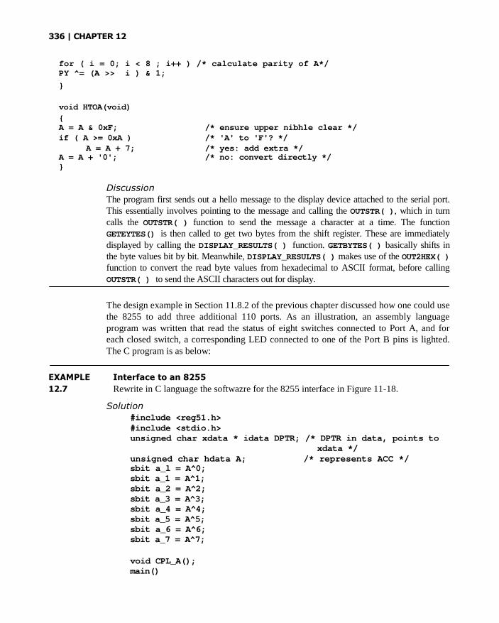
336 | CHAPTER 12
for ( i = 0; i < 8 ; i++ ) /* calculate parity of A*/PY ^= (A >> i ) & 1;
}
void HTOA(void)
{A = A & 0xF; /* ensure upper nibhle clear */if ( A >= 0xA ) /* 'A' to 'F'? */
A = A + 7; /* yes: add extra */A = A + '0'; /* no: convert directly */}
Discussion
The program first sends out a hello message to the display device attached to the serial port.This essentially involves pointing to the message and calling the OUTSTR( ), which in turncalls the OUTSTR( ) function to send the message a character at a time. The functionGETEYTES() is then called to get two bytes from the shift register. These are immediatelydisplayed by calling the DISPLAY_RESULTS( ) function. GETBYTES( ) basically shifts inthe byte values bit by bit. Meanwhile, DISPLAY_RESULTS( ) makes use of the OUT2HEX( )
function to convert the read byte values from hexadecimal to ASCII format, before callingOUTSTR( ) to send the ASCII characters out for display.
The design example in Section 11.8.2 of the previous chapter discussed how one could usethe 8255 to add three additional 110 ports. As an illustration, an assembly languageprogram was written that read the status of eight switches connected to Port A, and foreach closed switch, a corresponding LED connected to one of the Port B pins is lighted.The C program is as below:
EXAMPLE Interface to an 8255
12.7 Rewrite in C language the softwazre for the 8255 interface in Figure 11-18.
Solution#include <reg51.h>#include <stdio.h>unsigned char xdata * idata DPTR; /* DPTR in data, points to
xdata */unsigned char hdata A; /* represents ACC */sbit a_l = A^0;sbit a_1 = A^1;sbit a_2 = A^2;sbit a_3 = A^3;sbit a_4 = A^4;sbit a_5 = A^5;sbit a_6 = A^6;sbit a_7 = A^7;
void CPL_A();main()
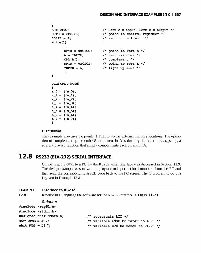
DESIGN AND INTERFACE EXAMPLES IN C | 337
{A = 0x90; /* Port A = input, Port B = output */DPTR = 0x0103; /* point to control register */*DPTR = A; /* send control word */while(1)
{DPTR = 0x0100; /* point to Port A */A = *DPTR; /* read switches */CPL_A(); /* complement */DPTR = 0x0101; /* point to Port E */*DPTR = A; /* light up LEDs */}
}
void CPL_A(void){a_0 = (!a_0);a_1 = (!a_1);a_2 = (!a_2);a_3 = (!a_3);a_4 = (!a_4);a_5 = (!a_5);a_6 = (!a_6);a_7 = (!a_7);}
Discussion
This example also uses the pointer DPTR to access external memory locations. The opera-tion of complementing the entire 8-bit content in A is done by the function CPL_A( ), astraightforward function that simply complements each bit within A.
12.8 RS232 (EIA-232) SERIAL INTERFACE
Connecting the 8051 to a PC via the RS232 serial interface was discussed in Section 11.9.The design example was to write a program to input decimal numbers from the PC andthen send the corresponding ASCII code back to the PC screen. The C program to do thisis given in Example 12.8.
EXAMPLE Interface to RS232
12.8 Rewrite in C language the software for the RS232 interface in Figure 11-20.
Solution
#include <reg5l.h>
#include <stdio.h>
unsigned char bdata A; /* represents ACC */sbit aMSB = A^7; /* variable aMSB to refer to A.7 */
sbit RTS = P1^7; /* variable RTS to refer to P1.7 */

338 | CHAPTER 12
sbit CTS = P1^6; /* variable CTS to refer to P1.6 */
bit C; /* represents carry bit */
unsigned char code * idata DPTR; /* DPTR in data, points to code */unsigned char code ASC[10] ={0x30, 0x31, 0x32, 0x33, 0x34, 0x35, 0x36,
0x37,0x38, 0x39; /* ASCII table */char code * MSG = {"PLEASE 1NTER NUMBER = "}; /* initial message */void FACE(void);void INCHAR(void); /* taken & modified from Example 8-7 */void OUTCHR(void); /* taken & modified from Example 8-6 */
void PARITY(void);
main(){FACE(); /* initialize serial port & do handshake */
DPTR = ASC; /* point to ASCII table */
while(1){INCHAR(); /* get decimal number and put in A */
A = DPTR[A]; /* convert to ASCII and store back in A */
OUTCHR(); /* output ASCII to serial port */
}}
void FACE(void){TMOD = 0x20; /* timer 1, mode 2 */TH1 = 0x98; /* reload count for 9600 baud */SC0N = 0x52; /* serial port, mode 1 */DPTR = MSG; /* pointer to initial message */TR1 = 1; /* start timer 1 */RTS = 0; /* assert RTS */while (CTS == 1); /* wait for CTS */do
{A = DPTR[A]; /* get ASCII characters */OUTCHR(); /* send out */DPTR++; /* if not end of message, get next character */}
while (A != 0); /* else if end of message, stop */}
void INCHAR(void){while (RI != 1); /* wait for character */
RI = 0; /* clear flag */

DESIGN AND INTERFACE EXAMPLES IN C | 339
A = SBUF; /* read char into A */
PARITY(); /* get even parity of A and put in AY */
C = PY; /* for odd parity in accumulator, PY shouldbe set */
C = !C; /* complementing correctly indicates if"error" */
aMSB = 0; /* strip off parity */
}
void OUTCHR(void)
{
PARITY(); /* get even parity of A and put in PY */
PY = !PY; /* change to odd parity */
aMSB = PY; /* add to character code */
while (TI != 1); /* Tx empty? no: check again */
TI = 0; /* yes: clear flag and */
SBUF = A; /* send character */
aMSB = 0; /* strip off parity bit */
}
void PARITY(void){int i;
PY = 0; /* initialize parity to 0 */
for ( i = 0; i < 8 ; i++ ) /* calculate parity of A*/
PY ^= ( A >> i ) & 1;
}
Discussion
This example employs familiar concepts such as using a temporary bit-addressable vari-able, A, to represent the accumulator, using an array in code memory to represent alookup table and using the pointer, DPTR, to access the lookup table. Besides that, werecall that in assembly language, we sometimes wish to store data in consecutive locationsin code memory by using the DE or DW assembler directives. This can be implemented inC by using an array that is stored in code memory.We also make use of the functionINCHAR( ), which is similar to the INCHAR( ) function discussed in Chapter 8, exceptthat since A is used instead of the accumulator, we need to compute the parity ourselvesby calling the PARITY( ) function, causing the parity to be stored in PY.
12.9 CENTRONICS PARALLEL INTERFACE
Printers interact with computers via the parallel port, and the common standard used iscalled the Centronics parallel interface. We demonstrated in the previous chapter aprogram to check the status of the printer before continually sending a test message to itfor printing. Example 12.9 shows just how this can be done in C.

340 | CHAPTER 12
EXAMPLE Interface to Centronics Parallel Interface
12.9 Rewrite in C language the software for the parallel interface in Figure 11-22.
Solution
#include <reg5l.h>#include <stdio.h>
unsigned char bdata A; /* represents ACC */unsigned char MASK = 0x3C; /* only check 4 of the bits */unsigned char OK = 0x30; /* normal values of the 4 status bits */sbit STR = P3^0;sbit ACK = P3^1;sbit BUSY = P3^2;char code * MSG = {"THIS IS A TEST FOR THE PRINTER"}; /* test msg */
unsigned char code * idata DPTR; /* DPTR in data, points to code */main()
{while (1)
{DPTR = MSG; /* point to test message */do{P3 = MASK; /* activate STROEE, P3.1-P3.5 as input */A = P3; /* read printer status */A = A & MASK; /* only P3.1-P3.5 are wanted */if (A != OK) /* any error? */
return; /* yes: stop */A = 0; /* no error, get ready to send */while (ACK == 1); /* before send, wait for ACK */
A = DPTR[A]; /* get char in test message */P1 = A; /* send char to printer */DPTR++; /* if not end, get next character */
while ( A != 0 ); /* else if end of message, stop */}
}
Discussion
Here, the 8-bit variable MASK is used to store the masking value, specifying which bits to bemasked off (ignored) by being cleared to zero. Bear in mind that a logical AND operationis denoted by one ampersand symbol "&" and not two. Two ampersands "&&" woulddenote a relational AND operator.

DESIGN AND INTERFACE EXAMPLES IN C | 341
12.10 ANALOG OUTPUT
Interfacing to an analog device often requires the use of ADCs and DACs. In Section 11.11,it was shown how to connect the 8051 to the MC1408L8 DAC to generate an analog sinewave by using a lookup table. Here we will present the corresponding C program.
EXAMPLE Analog Output
12.10 Rewrite in C language the software for the DAC interface in Figure 11-25.
Solution
#include <reg51.h>
#define MAX 1024
/* truncated TABLE of 1024 entries */unsigned char TABLE[MAX] = {127, 128, 129, 130, 131, ...};
int data STEP = 1; /* can he initialized to any increment value */unsigned char A; /* represents ACC */
int index = 0; /* use to point to entries in TABLE */
main( ){TMOD = 0x2; /* 8-bit, auto reload */
TH0 = -100; /* 100 ms delay */TR0 = 1; /* start timer */
IE = 0x82; /* enable timer 0 interrupt */while(1); /* main loop does nothing! */}
void T0ISR (void) interrupt 1{index = index + STEP; /* add STEP to index */if ( index > MAX )
index = 0; /* if end of TAELE, back to beginning */A = TABLE[index]; /* get entry */P1 = A; /* send it */
}
Discussion
The main program initializes the Timer 0, enables the corresponding Timer 0 interrupt, andthen does nothing. The bulk of the program lies in the Timer 0 interrupt function which, uponevery occurrence of the interrupt, accesses an entry from TABLE[], which is an array of 1024entries between 0 and 255 that correspond to the magnitudes of one period of a sine wave.(Notice that in the program above, TAELE[] is shown in truncated form.) When the end ofthe table is reached, the table index is reinitialized to 0 so that the next entry obtained

342 | CHAPTER 12
would again be starting from the beginning of the table. Prior to the running of this pro-gram, a separate program similar to that in Figure 11-24 is used to generate the 1024 en-tries of TABLE[].
12.11 ANALOG INPUT
Figure 11-27 demonstrated how an assembly language program is used to use an ADC toread and convert the voltage at a trimpot's center tap into digital form so that the correspon-ding ASCII code can be output to the console. Given here is the program rewritten in C.
EXAMPLE Analog Input
12.11 Rewrite in C language the software for the ADC interface in Figure 11-27.
Solution
#include <reg51.h>#define PORTA 0x101 /* 8155 Port A */
int xdata * idata DPTR; /* DPTR in idata, points to xdata */
unsigned char bdata A; /* represents ACC */sbit aMSB = A^7; /* variable aMSE to refer to A.7 */sbit aLSB = A^0; /* variable aLSE to refer to A.0 */sbit WRITE = P1^0; /* ADC0804 WR line */sbit INTR = P1^1; /* ADC0804 INTR line */
bit PY; /* represents parity bit */
char * BANNER = ("*** TEST ADC0804 ***\n"};void OUTSTR(void);void 0UTCHR(void);void OUT2HEX(void);void SWAP_A(void);void PARITY(void);void HTOA(void);
main()
{DPTR = BANNER; /* send message */OUTSTR();while (1)
{WRITE = 0; /* toggle WR line */WRITE = 1;while (INTR == 1); /* wait for INTR = 0 */DPTR = PORTA; /* knit DPTR -> Port A */A = *DPTR; /* read ADC0804 data */OUT2HEX(); /* send data to console */}
}
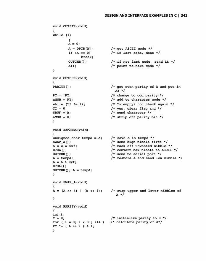
DESIGN AND INTERFACE EXAMPLES IN C | 343
void OUTSTR(void)
{while (1)
{A = 0;
A = DPTR[A]; /* get ASCII code */if (A == 0) /* if last code, done */
break;
OUTCHR(); /* if not last code, send it */A++; /* point to next code */
}
void OUTCHR(void){
PARITY(); /* get even parity of A and put inAY */
PY = !PY; /* change to odd parity */aMSB = PY; /* add to character code */
while (TI != 1); /* Tx empty? no: check again */TI = 0; /* yes: clear flag and */SBUF = A; /* send character */
aMSB = 0; /* strip off parity bit */
}
void OUT2HEX(void){unsigned char tempA = A; /* save A in tempA */SWAP_A(); /* send high nibble first */A = A & 0xf; /* mask off unwanted nibble */HTOA(); /* convert hex nibble to ASCII */OUTCHR(); /* send to serial port */A = tempA; /* restore A and send low nibble */A = A & 0xf;HTOA();OUTCHR(); A = tempA;}
void SWAP_A(void){
A = (A >> 4) | (A << 4); /* swap upper and lower nibbles ofA */
}
void PARITY(void){int i;Y = 0; /* initialize parity to 0 */for ( i = 0; i < 8 ; i++ ) /* calculate parity of A*/PY ^= ( A >> i ) & 1;}
344 | CHAPTER 12
void HTOA(void)
{A = A & 0xF; /* ensure upper nibble clear */if ( A >= 0xA ) /* 'A' to 'F'? */
A = A + 7; /* yes: add extra */A = A + '0'; /* no: convert directly */}
Discussion
The main program first displays a message to the console, and then toggles the WR line tobegin analog-to-digital conversion. It then waits for the ADC's INTR line to go low indi-cating that the conversion is complete before it reads data from the ADC via the 8155'sport A. The data is next converted to hexadecimal format before being sent out to theconsole for display.
12.12 INTERFACE TO SENSORS
In this section, we again discuss how the 8051 can interact with a typical sensor, the tem-perature sensor. Recall that in Chapter 11, we presented an assembly language program tomonitor the room temperature by using the DS1620 temperature sensor. When the roomtemperature is higher than 23°C, the furnace is turned on and the alarm sounds. If the tem-perature falls below 17°C, the furnace is switched off and the alarm is switched off. Weshow in Example 12.12 the corresponding C example to accomplish this.
EXAMPLE Interface to DS1620
12.12 Rewrite in C language the software for the sensor interface in Figure 11-29.
Solution
#include <reg5l.h>
#include <stdio.h>
unsigned char bdata A; /* represents ACC */
sbit aMSB = A^7; /* variable aMSB to refer to A.7 */
sbit aLSB = A^0; /* variable aLSB to refer to A.0 */
sbit DQ = P1^0;
sbit CLK = P1^1;
sbit RST = P1^2;
sbit THI = P1^3;
sbit TLO = P1^4;
sbit TC0M = P1^5;
sbit FURN = P1^6;
int i;
void SEND(void);
bit RRC_A(bit);

DESIGN AND INTERFACE EXAMPLES IN C | 345
main()
{
FURN = 0; /* turn furnace off */
RST = 1; /* initiate transfer */
A = 0xC; /* write config */
SEND(); /* send to DS1620 */
RST = 0; /* stop transfer */
RST = 1; /* initiate transfer */
A = 1; /* write TH */
SEND(); /* send to DS1620 */
A = 44; /* TH = 44 X 0.5 °C = 22 °C */
SEND(); /* send to DS1620 */
RST = 0; /* stop transfer */
RST = 1; /* initiate transfer */
A = 2; /* write TL */
SEND(); /* send to DS1620 */
A = 36; /* TL = 36 X 0.5 °C = 18 °C */
SEND(); /* send to DS1620 */
RST = 0; /* stop transfer */
RST = 1; /* initiate transfer */
A = 0xEE; /* start temperature sensing */
SEND(); /* send to DS1620 */
RST = 0; /* stop transfer */
while(1) /* keep sensing forever */
{
if (THI == 1) /* if T>= 22 °C, furnace = off */
FURN = 0;
if (TLO == 1) /* if T<= 18 °C, furnace = on */
FURN = 1;
}
}
void SEND(void)
{
for (i = 8; i > 0; i--) /* loop for all 8 bits */{CLK = 0; /* start clock cycle */CY = RRC_A(CY); /* rotate A into CY, LSB first */DQ = CY; /* send out bit to DB */CLK = 1; /* complete the clock cycle */}
}
346 | CHAPTER 12
bit RRC_A(bit C){bit tempBit;tempBit = C; /* backup C */C = aLSB; /* rotate A.0 into C */A = A >> 1; /* rotate A right */aMSB = tempBit; /* rotate C into A.7 */return C;}
Discussion
Most of the functionality in this example is done by the function send(), which serially(starting with the LSB) sends an 8-bit data to the port pin connected to the DQ (data) inputof the sensor.
12.13 INTERFACE TO RELAYS
In the last chapter, a very interesting application of relays was presented, that of a pedes-trian traffic light system. The 8051 electrically controlled the relay to switch between twostates, either to turn on the RED traffic light and GREEN pedestrian light in order to allowpedestrians to cross the road, or to turn on the GREEN traffic light and RED pedestrianlight. The program written in C to control all this is given in Example 12.13.
EXAMPLE Interface to a Relay: Pedestrian Traffic Light System
12.13 Rewrite in C language the software for the relay interface in Figure 11-33.
Solution
#include <reg51.h>
#include <stdio.h>
sbit LEDs = P1^0;
int thousand = 1000; /* 1000 X 10000 us = 10 secs */int count; /* to store the count values */
void delay(void);
main( )
{IE = 0x81; /* enable INT0 */
IT0 = 1; /* negative edge triggered */TMOD = 1; /* timer 0 in mode 1 */

DESIGN AND INTERFACE EXAMPLES IN C | 347
LEDs = 0; /* initially, traffic = GREEN,pedestrian = RED */
while (1); /* wait forever */}
void delay(void) /* 10-second delay */{for (count = thousand; count > 0; count —)
{TH0 = 0x6C;TL0 = 0x70;TR0 = 1;while(TF0 != 1);TF0 = 0;TR0 = 0;}
}
void EX0ISR(void) interrupt 0{LEDs = 1; /* traffic light = RED, pedestrian =
GREEN */delay(); /* wait 10 seconds */LEDs = 0; /* traffic light = GREEN, pedestrian =
RED */}
DiscussionComparing this program with its assembly language counterpart in the previous chapter, itwould seem that they are very similar. The only difference lies in the amount of delaygenerated by the delay( ) function, which is supposed to wait for 10 seconds to allowpedestrians to cross the road before the traffic and pedestrian lights switch back to theirinitial states. Nevertheless, the actual delay generated by this delay( ) function dependson which 8051 C compiler is used. In order to determine the exact amount of delaygenerated, we should view the corresponding assembly language instructions generated bythe compiler. In Keil's µVision2 IDE, this is done by choosing the Disassembly Windowfrom the View menu.
12.14 STEPPER MOTOR INTERFACE
The stepper motor finds interesting applications where precision-positioning of compo-nents is required. We saw in Chapter 11 an example assembly language program thatdemonstrated how to initially rotate a stepper motor clockwise, and whenever a switchconnected to external interrupt 0 (INT0) causes a high-to-low transition, the direction ofrotation should be reversed. In this section, we present the equivalent C program.

348 | CHAPTER 12
EXAMPLE Interface to a stepper motor
12.14 Rewrite in C language the software for the stepper motor interface in Figure 11-38.
Solution
#include <reg51.h>#include <stdio.h>
unsigned char A; /* ACC mirror */unsigned char tempA; /* temp variable */unsigned char code * idata DPTR; /* DATR in data, points to
code */bit D; /* direction bit for current
direction */int HUNDRED = 100; /* 100 X 10000 us = 1 sec */
/* 8-step sequence forclockwise rotation */
unsigned char code SEQ[8] = {0x9, 0x8, 0xC, 0x4, 0x6, 0x2,0x3, 0x1};
void CW(void);void CCW(void);void delay(void);
main()
{IE = 0x81; /* enable INTO */
IT0 = 1; /* negative edge triggered */TMOD = 1; /* timer 0 in mode 1 */D = 0; /* initialize D = 0 for
clockwise rotation */CW(); /* initial rotation is
clockwise */while(1) /* repeat forever */
{if (D != 1) /* previously clockwise? */
CCW(); /* no: change to clockwise */else
CW(); /* yes: change tocounterclockwise */
void CW(void) /* function for clockwiserotation */
{DATR = SEQ; /* point to start of table */for (A = 0; A < 8; A++)
{tempA = A; /* backup index in A */

DESIGN AND INTERFACE EXAMPLES IN C | 349
A = DPTR[A]; /* get step pattern into 4 LSBs ofA */
A = A | (P1&0xF0); /* retain 4 MSBs of A1 and put intoA */
P1 = A; /* send to stepper motor */delay(); /* wait for 1 sec */A = tempA; /* restore index into A */
}
}
void CCW(void) /*function for counterclockwiserotation */
{DPTR = SEQ; /* point to start of tahle */for (A = 7; A >= 0; A==)
{tempA = A; /* hackup index in A */A = DPTR[A]; /* get step pattern into 4 LSBs of
A */A = A | (P1&0xF0); /* retain 4 MSBs of P1 and put into
A */
P1 = A; /* send to stepper motor */delay(); /* wait for 1 sec */A = tempA; /* restore index into A */
}}
void delay(void) /* 1 second delay */
{for (tempA = HUNDRED; tempA > 0; tempA--)
{TH0 = 0x6C;TL0 = 0x70;TR0 = 1;while(TF0 != 1);TF0 = 0;TR0 = 0;
}
}
void EX0ISR(void) interrupt 0
{D = !D; /* complement direction bit */
}
Discussion
The program basically consists of the cw() and ccw() functions that directly interact withthe stepper motor and direct it to rotate clockwise and counterclockwise respectively. Theonly difference between these two functions, though, is just the sequence of step patternsbeing written to the stepper motor. In between the writing of a step pattern to the stepper

350 | CHAPTER 12
motor, the delay( ) function is called to give ample time for the stepper motor to digesteach step pattern.
PROBLEMS
12.1 Rewrite the software for the LCD to continually display the message "Welcome tothe 8051 Microcontroller Experience. Hope you enjoy your reading adventure."
12.2 Imagine that the stepper motor is used to automatically turn the knob of asafe. Based on a sequence of user-supplied numbers, the stepper motorturns the knob by the specified number of steps clockwise, then counter-clockwise, clockwise, etc. For example, if the sequence is 8, 0, 1, 6, 0, 9,9, then the stepper motor first turns clockwise by 8 steps, turns counter-clockwise by 0 steps, turns clockwise again by 1 step, and so on. Write afunction safe (int * seq, int seqsize) to receive as input a se-quence of numbers that have been stored in an array of size seqsize, andthen turns the stepper motor according to the input sequence. Assume theavailability of the CW () and the ccw ( ) functions.
12.3 The 8051 microcontroller is commonly used in smart cards, which are cards not onlywith built-in memory but also a built-in microcontroller as its brain, making itcapable of running programs from within itself. Some of the information containedin smart cards is confidential, hence there is a need for some form of protection fromunauthorized access. This is usually done by encrypting the information. Encryptionis the process of transforming confidential information (normally called theplaintext) into an unintelligible form (called the ciphertext). Once in this form, evenif someone were to eavesdrop or spy on it, he would not be able to understand itsmeaning. The only way to get back the original information is to perform the reverseprocess, called decryption. The Caesar cipher is one method of encryption that datesback to the days of the Roman empire, and is named after its inventor Julius Caesar.Though simple by today's standards, and no longer in use to protect information, anunderstanding of how it works helps to give us a basic idea of encryption. A moredetailed treatment of security and encryption will be given in Chapter 13.
Consider the English alphabet:
Imagine if we shifted all the alphabets 3 positions to the left, such that we obtain anew set of alphabets:
Then, given any confidential message, we replace each character from the first setof alphabets with a character from the second set of alphabets. For example, everyBA' we see will be replaced with a 'D', every 'B' with an BE', every 'C' with an 'F'and so on.
So the message:
would be encrypted to:

DESIGN AND INTERFACE EXAMPLES IN C | 351
Write a function CaesarEncrypt (char * plain, char * cipher) that takes in two messagestrings (arrays of characters), plain and cipher, respectively. Encrypt the message plainand save the encrypted message in cipher.
12.4 With reference to the previous question, write the corresponding function Caes - arDecrypt
(char * plain, char * cipher) to decrypt a message stored in cipher and save the decryptedmessage in plain.

352 | CHAPTER 12
Example Student Projects
13.1 INTRODUCTION
Students are often eager to do work on microcontroller and other robot-based projects.When assigned the task of constructing 8051-based projects, one often wonders in amaze-ment at the enthusiasm and keen interest shown by the students. The student reader hasalso seen some design and interface problems in Chapters 11 and 12. As an extension ofthat, we will attempt in this chapter to outline potential student projects that would help totie together all the concepts discussed in the earlier chapters of this book.
We will start with one of the simplest such projects: an 8051-based home securitysystem. Other more advanced-level projects would include a simple elevator system, aTic-TacToe game, an 8051-based calculator, a micromouse, a soccer-playing robot, and asmart card application.
13.2 HOME SECURITY SYSTEM
One of the simplest projects to build up the design skills in the student is the 8051-basedhome security system. This is basically a demonstration of how to interact with I/Odevices through the 8051's I/O ports.
13.2.1 Project Description
A sample project description for such a home security system could be:
Design an 8051 microcontroller-based home security system that has 64 Kbyte externalcode memory and 64 Kbyte external data memory. Assume you only have 8 K EPROMsand 8 K RAMs available.
353

354 | CHAPTER 13
Your security system should be able to detect when any of these sections of the househave been opened or intruded by a burglar:
1. gate2. front door3. back door4. any window
When one of them has been opened, turn on an alarm and also use a seven-segmentdisplay to display the corresponding house section. For example, if the gate is open,display 1. If any window is open, display 4.
13.2.2 System Specifications
The first thing for the student in tackling this project is to determine the required componentsfor the system. Based on the project description, it is clear that the following are needed:
1 x 8051 microcontroller 8 x 8Kbyte ROM/EPROM/EEPROM 8 x 8Kbyte RAM 4 x sensors 1 x alarm 1 x 7-segment display
The requirement was that the system should have 64 Kbyte of external codememory, but since only 8 Kbyte ROM chips are available, we would have to make dowith having eight of them in cascade. The same goes for implementing the external datamemory. We need to detect intrusions at four different points of the house as outlined inthe project description, hence we would need at least four sensors which could be infrared,light, or even switch sensors. Besides these, the project also requires the use of an alarmand a seven-segment display to indicate the point of intrusion. Notice that the list abovedoes not include the components needed for the external crystal clock circuit and resetcircuit. For details of such components, please consult Figure 2-2 in Chapter 2.
13.2.3 System Design
The next step involves making design choices to come up with a system that meets therequirements and specifications previously outlined. This includes deciding where to connectwhat to, what to use the 8051 I/O ports for; culminating in an overall schematic diagram show-ing the 8051 and how its pins (I/O, control, and clock) are connected to external memory andvarious 1/0 devices such as the sensors, alarm, and seven-segment display. Students might alsowant to use a 74LS47 BCD-to-seven-segment decoder to minimize the I/O port pins.
13.2.4 Software Design
Having decided on the hardware connections, the student can then proceed to designing andprogramming the software to control the 8051 and how it should interact with the externaldevices. This is often done with reference to the overall schematic diagram. Some questions
EXAMPLE STUDENT PROJECTS | 355
that you should ask yourself, and hence the corresponding programming decisions thatyou should make, include:
How should I sense the intrusion points? Via polling or interrupt? What priority should I assign to each intrusion point? When an intrusion occurs, what should I do? Should my system be programmed to detect more than one intrusion at a time? Should I include a capability to reset or deactivate the system? Should I allow the home owner to customize the system? Would the system have any security? For example, how should I ensure only the
home owner can customize or deactivate the system?
Often, in coming up with such questions, you need to put yourself in the shoes of theactual user to be able to better understand the situation and the problem that you aretrying to solve with the system.
Given below is a sample pseudo code for this home security system:Pseudo Code:
WHILE [1] DO BEGINWHILE [sensor == false] DO
[wait]CASE [sensor] OF
`gate': [display = 0]
frontdoor': (display = 1]`backdoor': [display = 2]`windows': [display = 3]
END_CASE[alarm = on]IF [reset == TRUE && password == TRUE]
THEN [alarm = off]END
The pseudo code above shows that the program is in an infinite loop. As long as no sensoris triggered, the program waits and does nothing. When a sensor is triggered, it is checkedto see which intrusion point it corresponds to, after which a number from 0 to 3 is displayedon the seven-segment display to indicate the point of intrusion. Next, the alarm is turned on.The program also allows for a reset mode where if the correct owner password is keyed in,the security system is reset and the alarm is turned off.
13.3 ELEVATOR SYSTEM
An elevator system is another interesting project that students could undertake. For sim-plicity, we will only consider a three-floor elevator system.
13.3.1 Project Description
The project description follows:
Design an 8051-based elevator system that supports three floors, namely ground, firstfloor, and second floor

356 | CHAPTER 13
Your system should consist of two parts:
1. Inside the ElevatorFigure 13-1 shows the inside of the elevator. The floor request buttons, G, 1, and 2, are used bythe elevator passenger to request the floor to which he wants to travel. The open (respectivelyclose) door buttons are used by the passenger to open (or close) the elevator door. Meanwhile,there is also a corresponding door open-close indicator, which is basically a series of eightLEDs arranged from left to right, flashing one at a time. When the flashing LED is leftmost, thisindicates that the door is closed. When the flashing LED is rightmost, the door is fully open.
2. Outside the ElevatorFigure 13-2 shows the outside of the elevator. The floor indicators are available at eachfloor to indicate whether the elevator is currently at that floor. The summon elevator but-tons are used by the waiting passenger outside the elevator to summon the elevator to hisfloors, and to indicate which direction the passenger wants to travel, up or down.
13.3.2 System Specifications
A thorough read through the project description reveals that we would require:
1 x 8051 microcontroller 9 x switch buttons (five for inside, four for outside)
FIGURE 13-1Inside the elevator
FIGURE 13-2Outside the elevator

EXAMPLE STUDENT PROJECTS | 357
11 x LEDs (eight for door open-close indicator, three for floor indicators) 1 x 7-segment display
It is clear that this project merely involves the interaction with switches and LEDs, plus aseven-segment display. Therefore, it is not much different from the home security systemin the previous section. The only thing here is that we are considering a totally differentscenario, and the sequence of happenings (opening door, elevator moving, etc.) is morecomplex than the home security system.
13.3.3 System Design
The system design stage in this case would involve deciding which port pins to connect tothe switch buttons, the LEDs, and the seven-segment display. Also, since the elevator sys-tem does not require the use of external memory, all four ports of the 8051 are availablefor I/O purposes so we have plenty to spare.
13.3.4 Software Design
The resultant program for this elevator system would be more complex because variousscenarios have to be considered, including:
Is the elevator currently on the same floor as that on which the up/down buttonrequest is made?
Is the elevator going in the same direction as the request? If not, but the requesting floor is nearer, would it stop and service this first or
ignore it and finish servicing an existing request? Would the elevator be servicing the nearest requesting floors first or would it be
constantly moving in one direction from the lowest requesting floor to thehighest, before changing direction and repeating the process?
If there is no request, what should the elevator be doing?
There are various alternatives to handling the problem and previous students have come upwith all sorts of ways to tackle this. A possible program could follow along the lines of thepseudo code below:Pseudo Code:
[start at ground floor]WHILE [1] DO BEGIN
WHILE [elevator summon == FALSE] DO[wait]
IF [summoning floor == current floor]THEN BEGIN
[door = open]WHILE [open door button == TRUE] DO
[wait][door = close]
END
[direction = up]
358 | CHAPTER 13
BEGIN
WHILE [ [summoning floor != current floor] &&[requested floor != current floor] ] DO BEGIN
IF [current floor == TOP_FLOOR]THEN [direction = down]
IF [current floor == TOP_FLOOR]
THEN [direction = up]IF [direction == up]
THEN [current floor = current floor + 1]ELSE [current floor = current floor - 1]
[floor indicator = current floor][floor display = current floor]
ENDBEGIN
[door = open]WHILE [open door button == TRUE] DO
[wait][door = close]END
ENDEND
Here, the current floor is the floor on which the elevator is currently at; thesummoning floor is the floor on which a waiting passenger outside the elevator haspressed the summon elevator button; while the requested floor refers to the floorrequested by the passenger from within the elevator by pressing the floor request button.
The program is in an infinite loop and the elevator is initially on the ground floor,waiting to be summoned by people who are in need of the elevator on their floor. Whenthe elevator is summoned, the program checks if the elevator is already on that floor, andif so would open the elevator door, wait for a while, and only close the door when theopen door button is no longer pressed. The elevator then moves up.
As the elevator is going up from one floor to the next, the program checks if thereare any elevator summons on the current floor, or if any passenger within the elevator hadrequested to go to that floor. If not, the elevator keeps going to the next floor. If thecurrent floor is already the top or bottom floor, the direction of travel is reversed. At thesame time, the floor indicators outside the elevator as well as the floor displays within theelevator would be updated to correspond to the current floor.
If the current floor is either the summoning floor or the requested floor, then the ele-vator opens its door, and waits for the passenger to release the open door button beforeit closes the elevator doors.
13.4 TIC-TAC-TOE
A more challenging project for students would be the development of games, and the corre-sponding artificial intelligence (AI) that would allow the program to compete with humans andwith each other. One such project is the developing the Tic-Tac-Toe game based on the 8051.

EXAMPLE STUDENT PROJECTS | 359
TABLE 13-1
Playing modes
MODE P1.3 (M1) P1.4 (M1)
0 - Human vs Human 0 01 - Human vs AI 0 12 - AI vs Human 1 0
13.4.1 Project Description
First, the project description and rules of the game have to be outlined: Design an 8051-
based Tic-Tac-Toe game that consists of two parts:
1. Tic-Tac-Toe Game EnvironmentAt the start of the game, the player(s) selects one of three playing modes: Human vsHuman, Human vs AI, and AI vs Human. The playing mode is input via two port pins, P1.3and P1.4, and is shown in more detail in Table 13-1.
There should be a 3 x 3 Tic-Tac-Toe panel (see Figure 13-3) to indicate which boxhas already been selected by a player. A selected box would either light up as yellow(Player 1) or red (Player 2). When a vertical, horizontal, or diagonal row of three boxes ofthe same color has been selected, the corresponding player wins the game. Otherwise, ifall boxes have been selected but no such row occurs, the game ends in a draw Each of thenine boxes basically consists of a yellow and red LED, and all these LEDs are connectedto the 8051 through Ports 0, 1, and 2 as indicated in Figure 13-4.
Each player takes turns to interact with a 3 x 3 matrix keypad to select a certain boxduring his turn. The connections of the 8051 to the keypad are via Port 3. Player 1indicates the end of his turn by setting P0.4 (Elf), which lights up an end-of-turn LED.Similarly, Player 2 ends his turn by setting his end-of-turn LED connected to P0.3 (E2).
At the end of the game, the results will be indicated on LEDs connected to P2.3 andP2.4, whose details are in Table 13-2.
2. Tic-Tac-Toe Artificial Intelligence (AI) ComponentThe Al component should be able to play as either player 1 or player 2 and should attemptas best as it could to win over the human player.
FIGURE 13-3Tic-Tac-Toe
1 2 3
4 5 6
7 8 9
pane

360 | CHAPTER 13
FIGURE 13-4Connecting the 8051 to the Tic-Tac-Toe pane
13.4.2 System Specifications
The Tic-Tac-Toe system consists of mostly LEDs and a 3 X 3 keypad for interacting withthe human player. A detailed list of components needed is as follows:
1 x 8051 microcontroller 1 x keypad (3 x 3) 11 x yellow LEDs 11 x red LEDs
TABLE 13-2Final results indicated on LEDs connected to P1.3 and P1.4
MODE P2.3 (F1) P2.4 (F0)
Player 1 (Yellow) Wins 1 0Player 2 (Red) Wins 0 1
Draw 1 1
EXAMPLE STUDENT PROJECTS | 361
So you see, there really is nothing much to the Tic-Tac-Toe hardware. What is more im-portant is the logical and clear organization of the LEDs to avoid confusions on the part ofthe human player.
13.4.3 Software Design
In writing the game environment component, some questions come to mind:
How do you determine the end of a player's turn? How should you check and hence run a playing mode? How do you determine if the game was won by a player or ended in a draw?
Meanwhile, for the AI part of the project:
How do you determine the best box position? How do you block an opponent's bid for a three-in-one row? Are there any more advanced and subtle techniques to fool the opponent into
selecting a box to your advantage? Should the AI strategy be fixed or should it adaptively change based on the
current situation?
The pseudo code for a possible Tic-Tac-Toe game environment is given below:Pseudo Code:
WHILE [input == FALSE][wait]
[current player = yellow]CASE [mode] OF
`0': BEGINWHILE [1] DO BEGIN
[check current player color]WHILE DO [player input == FALSE]
[wait][selected box == player color]IF [3-in-a-row == TRUE]
THEN BEGIN[display winner]
[end game]END
IF [all boxes selected == TRUE]THEN BEGIN
[display draw][end game]
ENDEND
END
`1': BEGIN[current player = human]WHILE [1] DO BEGIN
[check current player color]

362 | CHAPTER 13
IF [current player == AI]THEN [call AI]
WHILE DO [input == FALSE][wait]
[selected box == player color]IF [3-in-a-row == TRUE]
THEN BEGIN[display winner][end game]
ENDIF [all boxes selected == TRUE]
THEN BEGIN[display draw][end game]
ENDcurrent player = other player]
ENDEND
`2': BEGIN
[current player = AI]WHILE [1] DO BEGIN
[check current player color]IF [current player == AI]
THEN [call AI]WHILE DO [input == FALSE]
[wait][selected box == player color]IF [3-in-a-row == TRUE]
THEN BEGIN[display winner][end game]
ENDIF [all boxes selected == TRUE]
THEN BEGIN
[display draw][end game]
END[current player = other player]END
END
END_CASE
This program waits for the player to give an input to start playing Tic-Tac-Toe. Once aninput is detected, it checks to see what mode of play has been selected. If it is mode 0,which is "Human vs Human," then the program goes into an infinite loop and checks to seewho is the current player and waits for the current player to make his turn. When an inputhas been made, meaning a certain box has been selected, the program displays changes thecolor of that box to the corresponding color of the current player. After the current player

EXAMPLE STUDENT PROJECTS | 363
has taken his or her turn, the program checks to see if there are any three boxes of the samecolor in a vertical, horizontal, or diagonal row. In such a situation, the winner is displayedand the game ends. Otherwise, the program checks if all boxes have been selected, whichmeans that the game is a draw and this result is also displayed.
Otherwise, if mode 1, which is "Human vs AI," has been selected, the first player tostart is the human player. Going into an infinite loop, the program then checks the currentplayer. If the current player is the AI, the AI function would be called to calculate the bestbox to choose. Whether it is the AI or a human player, when a box has been selected by aplayer, it is displayed with the player's color. The program proceeds to check for threeequally-colored boxes in the same row, upon which it has detected a winner, displays theresult, and ends the game.
Mode 2 with "AI vs Human" is also similar to mode 1, with the difference that thefirst player to start is the AI.Meanwhile, the pseudo code for a possible Tic-Tac-Toe's AI is given below:Pseudo Code:
IF [opponent's 2-in-one row == TRUE]THEN [block opponent's chance]
ELSE BEGIN[calculate best box position]WHILE [box == taken] DO
[calculate next best box position][select box]END
The AI looks simple enough. The main priority is to first block an opponent's attempt atgetting three boxes in a row so if two boxes in a row are detected, then the AI's choicewould be to select the third box in order to block the attempt and prevent the opponentfrom winning. Next, if there are not two boxes in a row, that means the AI is still safe andhas more flexibility to choose a box based on its calculations. If the best box has alreadybeen taken, it calculates the next best box and so on until it finds a free box upon which itimmediately selects. Simple it may seem, but the real task of programming the AI lies inthe calculation of the best box positions. Here is what distinguishes the best AI fromamong the rest.
The separation of the software into two parts helps ease the programmer's task. Thisalso provides an interesting exercise on modular programming, where a program isdivided into modules, each written by a separate programmer. Once the programming isdone, the modules are integrated into one complete program. Modular programming allowsfor several parts of a program to be developed concurrently and is best suited for large andcomplex programming projects.
13.5 CALCULATOR
Calculators are so common these days that we sometimes tend to take them for granted. As afurther exercise in 8051-based system design and interfacing, an 8051-based would be a con-tenting project. Of course, to keep it simple, only the basic operations would be considered.
364 | CHAPTER 13
13.5.1 Project Description
The project description proceeds as follows:
Design an 8-bit 8051-based calculator to perform simple arithmetic operations such as:
Addition Subtraction
Multiplication Division Logical AND Logical OR Logical NOT Logical XOR Square Square root Cube Cubic root Inversion Exponentiation Factorial Modulo operation Percentage Pi Basic memory operations
Your calculator should be able to support 16-bit answers, which should be displayed oneither LCD or 7-segment displays. User input should be via a matrix keypad whose layoutshould be designed.
13.5.2 System Specifications
The calculator requires a matrix keypad for input, and either an LCD or seven-segmentdisplay for output. Besides these, there should at least be one push button switch forswitching on the calculator, and a corresponding LED to indicate that the calculator is on.Therefore, the components needed for this system would be:
1 x 8051 microcontroller 1 x matrix keypad 1 x LCD or 5 x 7-segment displays 1 x LED 1 x push button switch
13.5.3 Software Design
The software to control this system would be similar to that of operating systems such asWindows or MS-DOS, in which all arithmetic and logical operations as well as interactions

EXAMPLE STUDENT PROJECTS | 365
with input and output devices are handled by the program. In writing this program, the fol-lowing should be considered:
How do you determine if the key pressed by the user is a number or an operation? How should you handle operator precedence? Should you allow for accumulated operations? Should the calculator operate with unsigned or signed numbers? Should the calculator support decimal points? How would you implement each type of arithmetic or logical operation? Would you use lookup tables?
A possible 8051 calculator could operate based on the following pseudo code:Pseudo Code:
WHILE (1) DO BEGINWHILE [keypress == FALSE]
[wait]CASE [keypress] OF
`numeric': BEGIN
[save numeric value]
[format for 7-segment display][send to 7-segment display]END
`operation': BEGIN[determine operation][save operation]END
`memory operation': BEGIN[determine operation][perform operation]END
`equal': BEGIN
[recall saved numeric values and operations][perform operations]
[format result for 7-segment display][send to 7-segment display]END
END_CASEEND
The program waits indefinitely for a key press. When a key press is detected, it is checkedto see if it corresponds to a numeric value, arithmetic or logical operation, a memoryoperation, or the equal key. When the former two are detected, the program checksspecifically which value or operation they are and saves them. A numeric value wouldalso be formatted and sent to the seven-segment display. If a memory operation isrequested, the program immediately determines what memory operation is requested andservices it. Finally, if the equal key is pressed, it means the user is ready to see theresults, so all previously saved numeric values and operations are recalled and performedaccording to precedence. The result is then formatted and sent to the 7-segment display.
366 | CHAPTER 13
13.6 MICROMOUSE
When you connect the 8051 (the brain), some sensors (the eyes, ears, etc.), and some mo-tors (the hands and feet), you get a basic robot. One such robot is the micromouse, whichis the name for a robot that imitates a mouse and which tries to solve a maze. Solving amaze requires that the micromouse start from one end and slowly learn, mostly by trial anderror as well as memorizing, the correct path to the other end of the maze. Once it hasfound the correct path and reached the other end of the maze, it should be able to followthis path the next time it is put in the maze. Micromouse contests are popular and held inmany areas around the world. In this section, we will consider a micromouse project.
13.6.1 Project Description
As usual, we describe details of the project:
Design an 8051 microcontroller-based micromouse that should have the ability to moveforward, turn left and right as well as make U-turns. It should be able to solve a maze asfast as possible and once solved, should store the correct path in its memory.
13.6.2 System Specifications
In order to move forward and make turns, the micromouse should have two motors attached,respectively, to its left and right wheels. It should also be able to know if it has reached adead end, or if there is a wall on its left or right if it wanted to turn in that direction. For that,it would need some sensors. Two infrared sensors would suffice. Probably we could alsoinclude some LEDs to indicate what the micromouse is currently supposed to do, that iswhether it is going forward, turning left, right, or making a U-turn. The micromouse wouldalso need some large external memory for memorizing paths previously traversed. There-fore, the components for the micromouse are:
1 x 8051 microcontroller 2 x motors 2 x infrared sensors 1 x 64Kbyte RAM 2 x LEDs
13.6.3 System Design
The main part of the system design stage is to decide where to put the infrared sensors.The infrared sensor is typically made of two parts arranged side by side: an infrared LEDto emit infrared light and an infrared detector (phototransistor) to detect the presence ofany infrared light. If a wall is in the way of the sensor, the infrared light emitted by theinfrared LED would be reflected and subsequently detected by the infrared detector.Otherwise, if no wall is present, there would be no reflection and hence no infrared lightwould be detected. This is how the micromouse would know if there are any walls in acertain direction.
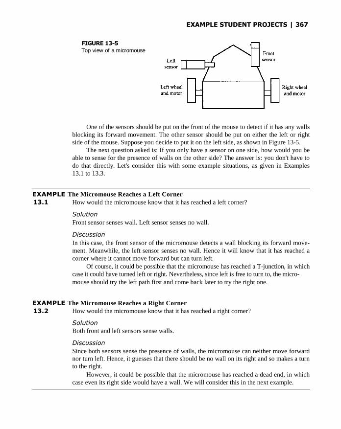
EXAMPLE STUDENT PROJECTS | 367
FIGURE 13-5
Top view of a micromouse
One of the sensors should be put on the front of the mouse to detect if it has any wallsblocking its forward movement. The other sensor should be put on either the left or rightside of the mouse. Suppose you decide to put it on the left side, as shown in Figure 13-5.
The next question asked is: If you only have a sensor on one side, how would you beable to sense for the presence of walls on the other side? The answer is: you don't have todo that directly. Let's consider this with some example situations, as given in Examples13.1 to 13.3.
EXAMPLE The Micromouse Reaches a Left Corner13.1 How would the micromouse know that it has reached a left corner?
Solution
Front sensor senses wall. Left sensor senses no wall.
Discussion
In this case, the front sensor of the micromouse detects a wall blocking its forward move-ment. Meanwhile, the left sensor senses no wall. Hence it will know that it has reached acorner where it cannot move forward but can turn left.
Of course, it could be possible that the micromouse has reached a T-junction, in whichcase it could have turned left or right. Nevertheless, since left is free to turn to, the micro-mouse should try the left path first and come back later to try the right one.
EXAMPLE The Micromouse Reaches a Right Corner13.2 How would the micromouse know that it has reached a right corner?
Solution
Both front and left sensors sense walls.
Discussion
Since both sensors sense the presence of walls, the micromouse can neither move forwardnor turn left. Hence, it guesses that there should be no wall on its right and so makes a turnto the right.
However, it could be possible that the micromouse has reached a dead end, in whichcase even its right side would have a wall. We will consider this in the next example.

368 | CHAPTER 13
EXAMPLE The Micromouse Reaches a Dead End13.3 How would the micromouse know that it has reached a dead end?
Solution
Previously, both front and left sensors sensed walls. After it makes a right turn, the frontsensor again senses a wall.
Discussion
Previously, both the front and left sensors sensed walls, so the micromouse turned right.However, after making the turn, its front sensor still senses a wall. This could only happenif it were at a dead end. In this case, it should turn right a second time, so that it has effec-tively made two right turns. This is essentially a U-turn. It can now proceed forward totrace back its steps and leave the dead end.
13.6.4 Software Design
The software for the micromouse is somewhat complicated and requires some deepthinking. Several issues include:
How would the micromouse detect left corners, right corners, and dead ends? How do you make the micromouse turn left or right? In what order should the micromouse test out all the possible paths? Should the
nearest or furthest branches be fully tested first? How should the micromouse remember previously traversed paths?
The pseudo code for the micromouse program is as follows:Pseudo Code:
WHILE [1] DO BEGIN[left motor = right motor = forward]IF [front sensor == wall]
IF [left sensor == no wall]THEN BEGIN
[left motor = backward][right motor = forward]
ENDELSE BEGIN
[left motor = forward][right motor = backward]IF [front sensor == wall]
THEN BEGIN[left motor = forward][right motor = backward]
ENDEND
[memorize path]END
The issue of detecting corners and dead ends has just been discussed in Examples 13.1 to 13.3.What about turning left and right? This can easily be solved. If the micromouse is to go forward,

EXAMPLE STUDENT PROJECTS | 369
both motors should turn forward. If it wants to go left, the left motor should go backwardswhile the right motor should go forward. Similarly, to turn right, the left motor should goforward while the right motor should go backwards.
The pseudo code above shows that the program goes into an infinite loop, and ini-tially goes forward. If it senses a wall in front, it proceeds to sense if there is a wall on itsleft. If not, it turns left. Otherwise, it turns right. After turning right, it senses if there is awall in front. If there still is then it is at a dead end, so it turns right again. Now that it hasdone the required turns, it can proceed to go forward. During all this while, themicromouse is also memorizing the paths that it has previously traversed.
The main challenge in programming the micromouse lies in the one line: [memorizepath]. How should the micromouse memorize the paths to ensure that the next time itcomes to the same T-junction or crossroad, it would not choose paths with dead ends?This will be the subject of immersing thought and vigorous programming trials.
13.7 A SOCCER-PLAYING ROBOT
The previous section discussed how an 8051 could be used as the brain for a mouse-likerobot, enabling it to find its way through a maze and hence solve it. In fact, the 8051 canbe used to control any robot, and is among the popular microcontrollers that are used byrobot enthusiasts as robot brains. Robot contests are held around the world, and are veryinteresting sights indeed. Participating robots would be required to do all sorts of tasksranging from playing simple sports to more complicated tasks such as climbing stairs. Inthis section, we will discuss how an 8051 is used to control a soccer-playing robot.
13.7.1 Project Description
Design an 8051 microcontroller-based robot to take part in a robo-soccer contest, lasting 10minutes. During each match, two robots playing as blue and red are put in a grey-carpetedarena with randomly placed blue and red balls of 15mm in diameter. A common goal is lo-cated at one end of the arena and is illuminated by bright lights. Each robot should detect thepresence of balls, sense the ball colors, and collect balls of its own color. However, it shouldonly store one ball at a time. Once it has collected a ball, it should search for the commongoal and kick the ball into the goal.
13.7.2 System Specifications
Similar to the micromouse, the robot should have wheels attached to motors. It wouldalso need some light sensors (LED and phototransistor pairs) to detect the goal, and ballcolors, plus some contact sensors such as switches to detect walls or the opponent robot.Since the robot is to stand alone, it should have nonvolatile memory. In this case, anEPROM would be a good choice since this would allow the program to be overwritten atwill, which is often desirable. The required components are then:
1 x 8051 microcontroller 2 x motors 4 x wheels
370 | CHAPTER 13
2 x light sensors (LED and phototransistor pair) 4 x switches 1 x EPROM
13.7.3 System Design
In designing this robot system, where to put the light and contact sensors is important. Forexample, the light sensors to sense the ball colors should be well shaded from their exter-nal surroundings, otherwise it would affect the color detection. This is especially so whenthe robot is very near the goal. The brightness of the goal lights would interfere with thelight from the sensor's LED and cause confusion.
Another design issue is the kicking mechanism. Various methods exist to kick theball, and watching different students think up different ideas would be part of the fun.Some would use motors to swing a shaft to make contact with the ball, similar to howbaseball players hit with their bats. However, the limitation of this technique is that thekick would be less powerful than if an elastic energy were used. Hence, some would preferto attach the shaft to a piece of rubber band, and use a motor to stretch it. Then when therobot is ready to kick, the motor moves into a position such that the rubber band isreleased, forcing the shaft to swing towards the ball and kick it out of the robot.
13.7.4 Software Design
Some issues related to the robot software are:
How would the robot detect walls and opponent robots? How should the robot turn? When the robot reaches a corner, should it turn right or left? Should it always turn
to one direction or should it alternate, or turn randomly? How should randomness be implemented? How would the robot detect ball colors? How would the robot detect the direction of the goal? How should the robot kick? What strategy should the robot use against its opponent? Should it be more offen-
sive, defensive, or switch strategies halfway through the match? How should the robot move around the arena? Should it move randomly, or
should it move in a certain pattern? If so, what would be the best pattern to ensurethat it covers as much ground as possible?
Given below is a sample pseudo code for the robot playing blue:Pseudo Code:
WHILE [1] DO BEGIN[walk in spiral pattern]IF [contact sensor == TRUE]
THEN BEGIN[reverse][turn left or right]
END

EXAMPLE STUDENT PROJECTS | 371
IF [light sensor == BLUE]IF [balls collected < 1]
THEN BEGIN[collect ball][sense goal lights]
IF [goal detected == TRUE]THEN BEGIN
[stop][kick]
ENDEND
IF [light sensor == RED]IF [time left == 5 minutes]
IF [balls collected < 1]THEN BEGIN
[collect ball]
[go straight forward]IF [wall detected]
[release ball]END
END
The program directs the robot to walk in a spiral pattern, believed by some to be agood pattern that allows the robot to cover much ground. When a contact sensor returnsTRUE, this indicates that it has either moved against a wall or an opponent, upon whichthe robot reverses and either turns right or left, away from the obstacle, before proceedingwith its forward movement. If the light sensor detects a BLUE ball, which is its own color,it checks to see if it already has a ball within its storage. Otherwise, it collects the ball andimmediately goes in search of the goal. Once the goal is detected, the robot stops and kicksthe ball in. If the light sensor senses a RED ball, the robot checks if there are only 5 min-utes left in the match. If so, it will switch to a more offensive strategy where it collects anopponent ball, goes straight forward, expecting to bump into a wall sooner or later. Whenit does, it releases the ball. Balls right next to the wall are usually much harder to collect.This would be the BLUE robot's strategy against the opponent.
13.8 A SMART CARD APPLICATION
Microcontrollers are finding increasing usage in smart cards, which are cards that inte-grate both memory and a microcontroller within its physical limits. Imagine having acomputer so small that we can wrap it up with a piece of plastic that fits into our wallet:That's a smart card. Smart cards are being used as national identity cards, drivinglicenses, passport information, and electronic cash (e-cash). Since these smart cardscontain personal as well as sensitive financial information, and would be issued to thepublic, it is vital that the information contained within it be protected from beingaccessed or tampered with by unauthorized parties. The following subsection brieflydescribes basic security concepts for a better understanding of how the informationwithin smart cards can be protected.
372 | CHAPTER 13
13.8.1 Basic Security Concepts
Information security typically requires that confidentiality, authentication, and integrityto be guaranteed. Confidentiality ensures that only authorized parties can access and viewthe information. Authentication proves the identity of a party while integrity allows one todetermine whether information has been modified without permission.
All these are possible by using cryptographic techniques such as encryption,digital signatures, and message authentication. Encryption is the process of trans-forming some confidential information into unintelligible form in order to protect itfrom being accessed. Standard encryption methods are the Data Encryption Standard(DES) and its variant, the triple-DES. Incidentally, the latter is also used in many cur-rent Automatic Teller Machine (ATM) cards to protect the user Personal IdentificationNumbers (PINs).
Meanwhile, a digital signature is similar in concept to its physical handwritten coun-terpart. However, instead of using a handwritten signature or a thumbprint, a digital signa-ture uses some bits of secret data to prove the identity of a party. Message authentication isdone by using some secret bits of data to perform an operation on the message to obtainwhat is called a message authentication code (MAC). This is similar to a checksum andis used to check if the message has been modified. Since the MAC can only be obtainedwhen you know the secret data, this ensures that unauthorized parties cannot modify themessage without being detected because the MAC would be different.
13.8.2 Project Description
Recall that in the problems section of the previous chapter, we discussed a very simpleencryption method called the Caesar cipher. We will now consider a slightly more com-plicated and generalized version, the polyalphabetic cipher. Even so, this encryptionmethod is also not in use today to protect information because it is very easy to crack byusing computer programs. However, for ease of illustration, we will consider it in thissection, and only touch on currently secure methods in the problems section at the end ofthis chapter.The polyalphabetic cipher is similar to the Caesar cipher except that instead of shiftingthe original plaintext set of alphabets a fixed three positions to the left, it is shifted left bya variable number of positions. For example, shifting by 10 positions to the left, theplaintext alphabet set would be replaced by a ciphertext alphabet set as follows:Plaintext alphabets A B C D E F G H I J K L M N O P Q R S T U V W X Y ZCiphertext alphabets K LM N O P Q R S T U VW X Y ZA B C D E F G H I Jso the message THIS IS SECRET is encrypted into DRSC SC COMBOD.Design an 8051 microcontroller-based smart card that encrypts by using the polyalpha-betic cipher, null-terminated messages stored in its EPROM starting at location 1234H.
13.8.3 System Specifications
The smart card system is really quite simple, consisting of just the 8051 and an EPROM,whether external or built into the microcontroller, in which case we would be using an 8071
EXAMPLE STUDENT PROJECTS | 373
instead of an 8051. We might choose to add in some extra features, for example an LCDto display both plaintext and ciphertext messages. The components are:
1 x 8051 microcontroller 1 x EPROM 1 x LCD
13.8.4 Software Design
When writing the encryption software, several issues might be:
How would the number of shifts be determined? Would it be randomly chosen, orwould the user be allowed to specify?
Are there any number of shifts that should not be permitted? For example, shiftingby 0, 26, 52, or any multiple of 26 positions would cause the ciphertext to beexactly the same as the ciphertext, resulting in no encryption at all.
Pseudo Code:
BEGIN[determine number of shifts][location = 1234H]REPEAT
BEGIN
[get character from location][encrypt character]
[store back in location]END
UNTIL [character == NULL]END
The software is straightforward enough. First, the number of shifts is determined, and thefirst location is set to 1234H. The program then gets a character from the current location,encrypts it with the polyalphabetic cipher and stores the encrypted character back into thecurrent location, hence overwriting the previously stored character. This is repeated until aNULL character is detected, indicating the end of the message.
SUMMARY
We have described some advanced 8051-based projects that we feel would be challengingas well as interesting to students. Possible solutions are discussed in an orderly fashionstarting from a careful study of the project description to a specification of the systemrequirements and components. This is followed by a subsection on software design whichconsiders some programming decisions and the corresponding pseudo code description ofthe software.

374 | CHAPTER 13
PROBLEMS
13.1 Draw the schematic diagram for the home security system project in Section 13.2showing all the connections between the 8051 and the alarm, sensors, seven-segment display, and external memory chips. Hence, write the software (inassembly or C) to control this system.
13.2 Draw the schematic diagram for the elevator system project in Section 13.3 show-ing all the connections between the 8051 and the LEDs, switches, and seven-segment display.
13.3 Observe the behavior of several elevator systems in your university or any buildingnear you. In what order do these systems service the elevator requests? Why do youthink such an order is used?
13.4 Draw the schematic diagram for the Tic-Tac-Toe project in Section 13.4 showingall the connections between the 8051, the keypad, the LEDs, and switches. Hence,write the software (in assembly or C) for this system.
13.5 Draw the schematic diagram for the calculator project in Section 13.5 showing allthe connections between the 8051 and the keypad, display, LED, and switch.
13.6 Write the assembly language subroutine or C function to perform any two of thearithmetic operations listed in the project description of the 8051 calculator.
13.7 Draw the schematic diagram for the micromouse project in Section 13.6 showingall the connections between the 8051 and the motors, sensors, LEDs, and externalmemory.
13.8 Give some thought to the problem of programming the micromouse:a. Testing out all possible paths: In which order do you think they should be
tested out? Nearest branches first, or the furthest? Why?b. Memorizing previously traversed paths: What do you think is the best way for
the micromouse to achieve this? Why?13.9 When using smart cards for personal identification, it is often desired that the photo
of the individual also be embedded within the card. However, one limitation of thesmart card is its small memory size. Research currently used techniques of embed-ding photos into smart cards.
13.10 One day in class, you chance upon a folded piece of paper, written by a certainclassmate to another classmate of the opposite sex. "Interesting," you think toyourself as the smile on your face widens. But the smile turns to disbelief when yousee that the rest of the message reads as follows:
atih spit idcxywi
You have just learnt about the Caesar cipher in class the other day, so you guessthat the classmate must have used that. But after sitting down and trying todecipher the message, you find that it was not the Caesar cipher. Nevertheless, youare sure it must be something similar, just that unlike the Caesar cipher where youshift by three positions to the right, you do not know how many shifts yourclassmate used. A polyalphabetic cipher was used!Suddenly it dawns on you: use the 8051 to decipher it! Write an 8051 program todecipher the message.

EXAMPLE STUDENT PROJECTS | 375
Hint: You would need to perform what we call a dictionary attack: Try all possible shifts andcompare each deciphered word with words in a dictionary to see if you get any matches. Once youget matches for all three words, you have most probably deciphered the message successfully.Assume that you have a dictionary with 1000 entries including the words of the original message,and which is represented by the following array of characters:
char * d ic t ionary = { "a" , "ab le " , "about " , . . . } ;
where dictionary [0] gives you "a" , dictionary [1] gives you "able", etc.Assume all characters are in lowercase, with the ASCII codes given in the table below:
TABLE 13-3 Partial ASCII table
ASCII Code
Character Decimal Hex Binary
a 97 61H 01100001b 98 62H 01100010
c 99 63H 01100011
d 100 64H 01100100
e 101 65H 01100101
f 102 66H 01100110
g 103 67H 01100111
. . .
Write the pseudo code for such a program.13.11 Write the corresponding 8051 C solution to Problem 13.10. Hence, use it to decode the message.
13.12 The Advanced Encryption Standard (AES) is a recent encryption standard chosen to replace theDES and triple-DES in future security applications. Research on how the AES works and write an8051 program (whether in assembly or C) to implement the AES. A brief description of the AESis also given in Appendix J.

376 | CHAPTER 13

8051 Derivatives
14.1 INTRODUCTION
Since the advent of the MCS-51TM family of microcontroller ICs, newer and more advancedversions have sprung up. These 8051 derivatives have additional memory, built-in I/0 suchas ADCs and DACs, and other extended peripherals. In this section, we will briefly reviewsome of these derivatives.
14.2 MCS-151TM AND MCS-251TM
Intel has produced advanced versions of the MCS-51TM family. These are the MCS-151TM,with five times increased performance, followed by the MCS-251TM family with 15 timesperformance increase. The MCS-251 TM family has an advanced architecture that increasesthe efficiency for 8051 C language programming, an extended instruction set that includes16- and 32-bit arithmetic and logic instructions, plus increased memory size options (seeTable 14-1). Here, One-Time Programmable (OTP) ROM refers to EPROM-like codememory but without the quartz glass window for erasing the contents. This reduces thepackaging cost but prevents the OTP ROM from being erased with ultraviolet (UV) light;hence, it can only be programmed once. ROMless versions are also available.
14.3 MICROCONTROLLERS WITH FLASH MEMORYAND NVRAM
In Chapter 2 we were introduced to the MCS-51TM with different types of on-chip codememory ranging from the ROMless 8031, through to the 8051 with on-chip ROM, andthe 8751 with on-chip EPROM.
377
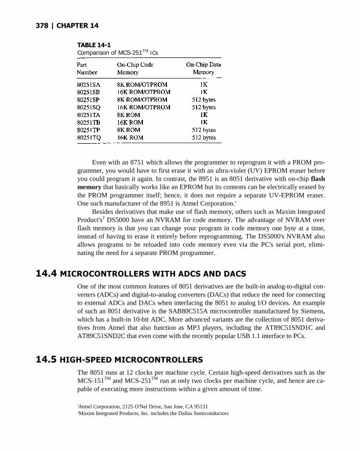
378 | CHAPTER 14
TABLE 14-1Comparison of MCS-251TM ICs
Even with an 8751 which allows the programmer to reprogram it with a PROM pro-grammer, you would have to first erase it with an ultra-violet (UV) EPROM eraser beforeyou could program it again. In contrast, the 8951 is an 8051 derivative with on-chip flashmemory that basically works like an EPROM but its contents can be electrically erased bythe PROM programmer itself; hence, it does not require a separate UV-EPROM eraser.One such manufacturer of the 8951 is Atmel Corporation.'
Besides derivatives that make use of flash memory, others such as Maxim IntegratedProduct's2 DS5000 have an NVRAM for code memory. The advantage of NVRAM overflash memory is that you can change your program in code memory one byte at a time,instead of having to erase it entirely before reprogramming. The DS5000's NVRAM alsoallows programs to be reloaded into code memory even via the PC's serial port, elimi-nating the need for a separate PROM programmer.
14.4 MICROCONTROLLERS WITH ADCS AND DACS
One of the most common features of 8051 derivatives are the built-in analog-to-digital con-verters (ADCs) and digital-to-analog converters (DACs) that reduce the need for connectingto external ADCs and DACs when interfacing the 8051 to analog I/O devices. An exampleof such an 8051 derivative is the SAB80C515A microcontroller manufactured by Siemens,which has a built-in 10-bit ADC. More advanced variants are the collection of 8051 deriva-tives from Atmel that also function as MP3 players, including the AT89C51SND1C andAT89C51SND2C that even come with the recently popular USB 1.1 interface to PCs.
14.5 HIGH-SPEED MICROCONTROLLERS
The 8051 runs at 12 clocks per machine cycle. Certain high-speed derivatives such as theMCS-151TM and MCS-251TM run at only two clocks per machine cycle, and hence are ca-pable of executing more instructions within a given amount of time.
'Atmel Corporation, 2125 O'Nel Drive, San Jose, CA 951312Maxim Integrated Products, Inc. includes the Dallas Semiconductors

8051 DERIVATIVES | 379
Maxim also produces various types of 8051 derivatives, including high-speed micro-controllers, network microcontrollers, and secure microcontrollers. Its high-speed microcon-troilers run at four clocks per machine cycle compared to the 8051's 12 clocks, while its ultrahigh-speed microcontroller, the DS89C420, runs at one clock per machine cycle. Other en-hancements over the 8051 include more interrupt sources and increased memory sizes.
14.6 NETWORK MICROCONTROLLERS
The network microcontrollers manufactured by Maxim support various network protocolssuch as the Ethernet and Controller Area Network (CAN). Other network microcontrollerssuch as the 83751 by Philips3 support the Inter-Integrated Circuit (I2C) network interfacewhile the COM20051 by Standard Microsystems4 supports the ARCNET token ring net-work protocol. Such network protocols allow several microcontrollers and other processorsto be connected as a network to share and exchange data. Atmel's ATWebSEG-32 is an8051 derivative that supports internet connection (TCP/IP) and the Ethernet.
14.7 SECURE MICROCONTROLLERS
In the previous chapter, we had a look at how the 8051 can be used as the brain in smartcards. This included a discussion of how confidential information could be protected viasoftware encryption. In fact, encryption can be done by dedicated security hardware, andseveral 8051 derivatives such as Maxim's secure 8051 microcontrollers have been pro-duced to achieve this.
The security system in the smart card that allows encryption, digital signatures,and message authentication to be performed is commonly called a public-keyinfrastructure (PKI). This PKI is commonly embedded within secure microcontrollersand is supported by hardware peripherals built into these microcontrollers, for instanceMaxim's DS5240, which has a Modulo Arithmetic Accelerator (MAA) to supportmodulo arithmetic operations, used extensively in PKIs. Other secure microcontrollerssuch as Maxim's DS5000 support hardware encryption of the programs loaded into itscode memory. By encrypting these programs, even if the smart card is tampered withand its programs accessed without authorization, the attacker would not be able tounderstand the meaning of the programs.
SUMMARY
In this chapter, we have described the many derivatives of the 8051. These enhanced ver-sions of the 8051 typically have better types of on-chip memory, larger memory size,higher speed, and more built-in peripherals to support interactions with analog I/O devices,network, and security applications.
3Philips Semiconductors, 811 E. Argues Avenue, Box 3409, Sunnyvale, CA 940884Standard Microsystems Corporation, 80 Arkay Drive, Hauppauge, NY 11788
380 | CHAPTER 14
That being said, the final decision of selecting the most suitable 8051 or derivativefor your project depends on a set of criteria such as the amount and type of on-chip ROMand RAM, speed, as well as advanced I/O, network, and security requirements.
PROBLEMS
14.1 Conduct research on the various 8051 derivative manufacturers and list out other de-rivatives with built-in ADCs or DACs.
14.2 Conduct research on the 8051 manufacturers and list out other secure microcon-trollers. Include their security features.
14.3 Are there other enhancements to the 8051 that are not discussed in this chapter? Listout the enhancements if any, and examples of such derivatives.

Quick Reference Chart
MNEMONIC DESCRIPTION MNEMONIC DESCRIPTION
Arithmetic OperationsADD A,source add source to AADD A,#dataADDC A,source add with carryADDC A,#dataSUBB A,source subtract from ASUBB data with borrowINC A incrementINC sourceDEC A decrementDEC sourceINC DPTR increment DPTRMUL AB multiply A & BDIV AB divide A by BDA A decimal adjust A
Logical OperationsANL A,source logical ANDANL A,#dataANL dlrect,AANL direct,#dataORL A,source logical ORORL A,#dataORL direct,AORL direct,#dataXRL A,source logical XOR
XRL A,#dataXRL direct,AXRL direct,#dataCLR A clear ACPL A complement ARL A rotate A leftRLC A (through C)RR A rotate A rightRRC A (through C)SWAP A swap nibbles
LEGEND
Rn register addressing using R0-R7direct 8-bit internal address (00H-0FFH)@Ri indirect addressing using R0 or R1source any of [Rn,direct,@Ri]dest any of [Rn,direct,@Ri]#data 8-bit constant included in inst.#data 16 16-bit constantbit 8-bit direct address of bitrel signed 8-bit offsetaddr11 11-bit address in current 2k pageaddr16 16-bit address
FIGURE A-1
Quick reference chart
381

382

Opcode Map
383

3
84
Instruction Definitions1
LEGEND
Symbol Interpretation
is replaced by ...() the contents of . . .(( )) the data pointed at by . . .rrr one of eight registers; 000 = R0, 001 = R1, etc.dddddddd data bitsaaaaaaaa address bitsbbbbbbbb address of a bit
indirect addressing using R0 (i = 0) or R1 (i = 1)eeeeeeee 8-bit relative address
ACALL addr11
Function: Absolute Call
Description: ACALL unconditionally calls a subroutine located at the indicatedaddress. The instruction increments the PC twice to obtain the addressof the following instruction, then pushes the 16-bit result onto thestack (low-order byte first) and increments the stack pointer twice.The destination address is obtained by successively concatenating thefive high-order bits of the incremented PC, opcode bits 7-5, and thesecond byte of the instruction.
1Adapted from 8-Bit Embedded Controllers (270645). Santa Clara, CA: Intel Corporation, 1991, by permission
of Intel Corporation.
385

386 | APPENDIX C
The subroutine called must therefore start within the same 2K block ofthe program memory as the first byte of the instruction followingACALL. No flags are affected.
Example: Initially SP equals 07H. The label "SUBRTN" is a program memorylocation 0345H. After executing the instruction,
ACALL SUBRTN
at location 0123H, the SP contains 09H, internal RAM locations 08Hand 09H contain 25H and 01H, respectively, and the PC contains0345H.
Bytes: 2
Cycles: 2
Encoding: aaal000l aaaaaaaa
Note: aaa = A10-A8 and aaaaaaaa = A7-A0 of thedestination address.
Operation: (PC) (PC) + 2
(SP) (SP) + 1
((SP)) (PC7-PC0)
(SP) (SP) + 1
((SP)) (PC15-PC8)
(PC10-PC0) page address
ADD A,<src-byte>
Function: Add
Description: ADD adds the byte variable indicated to the accumulator,leaving theresult in the accumulator. The carry and auxiliary-carry flags are set,respectively, if there is a carry-out from bit 7 or bit 3, and clearedotherwise. When adding unsigned integers, the carry flag indicates anoverflow occurred.
OV is set if there is a carry-out of bit 6 but not out of bit 7, or a carry-out of bit 7 but not out of bit 6; otherwise OV is cleared. When addingsigned integers, OV indicates a negative number is produced as thesum of two positive operands, or a positive sum from two negativeoperands.
Four source-operand addressing modes are allowed: register, direct,register-indirect, or immediate.
Example: The accumulator holds 0C3H (11000011B) and register 0 holds 0AH(10101010B). The instruction,

INSTRUCTION DEFINITIONS | 387ADD A,R0
leaves 6DH (01101110B) in the accumulator with the AC flag clearedand both the carry flag and OV set to 1.
ADD A,Rn
Bytes: 1
Cycles: 1
Encoding: 00101rrr
Operation: (A) (A) + (Rn)
ADD A,direct
Bytes: 2
Cycles: 1
Encoding: 00100101 aaaaaaaa
Operation: (A) (A) + (direct)
ADD A,@Ri
Bytes: 1
Cycles: 1
Encoding: 0010011i
Operation: (A) (A) + ((Ri))
ADD A,#data
Bytes: 2
Cycles: 1
Encoding: 00100100 dddddddd
Operation: (A) (A) + #data
ADDC A,<src-byte>
Function: Add with Carry
Description: ADDC simultaneously adds the byte variable indicated, the carry flag,and the accumulator contents, leaving the result in the accumulator.The carry and auxiliary-carry flags are set, respectively, if there is acarry-out from bit 7 or bit 3, and cleared otherwise. When addingunsigned integers, the carry flag indicates an overflow occurred.
388 | APPENDIX C
OV is set if there is a carryout of bit 6 but not out of bit 7, or a carry-out of bit 7 but not out of bit 6; otherwise OV is cleared. When addingsigned integers, OV indicates a negative number is produced as thesum of two positive operands, or a positive sum from two negativeoperands.
Four source-operand addressing modes are allowed: register, direct,register-indirect, or immediate.
Example: The accumulator holds 0C3H (11000011B) and register 0 holds 0AAH(10101010B) with the carry flag set. The instruction,
ADDC A,Rn
leaves 6EH (01101110B) in the accumulator with AC cleared and boththe carry flag and OV set to 1.
ADDC A,Rn
Bytes: 1
Cycles: 1
Encoding: 00110rrr
Operation: (A) (A) + (C) + (Rn)
ADDC A,direct
Bytes: 2
Cycles: 1
Encoding: 00110101 aaaaaaaa
Operation: (A) (A) + (C) + (direct)
ADDC A,@Ri
Bytes: 1
Cycles: 1
Encoding: 0011011i
Operation: (A) (A) + (C) + (Ri)
ADDC A,#data
Bytes: 2
Cycles: 1
Encoding: 00110100 dddddddd
Operation: (A) (A) + (C) + #data

INSTRUCTION DEFINITIONS | 389
AJMP addr11
Function: Absolute Jump
Description: AJMP transfers program execution to the indicated address, which isformed at run-time by concatenating the high-order five bits of the PC(after incrementing the PC twice), opcode bits 7-5, and the secondbyte of the instruction. The destination must therefore be within thesame 2K block of program memory as the first byte of the instructionfollowing AJMP.
Example: The label "JMPADR" is at program memory location 0123H. Theinstruction,
AJMP JMPADR
is at location 0345H and loads the PC with 0123H.
Bytes: 2
Cycles: 2
Encoding: aaa0000l aaaaaaaa
Note: aaa = A10-A8 and aaaaaaaa = A7-A0 of the destination address.
Operation: (PC) (PC) + 2
(PC10-PC0) page address
ANL <dest-byte>,<src-byte>
Function: Logical-AND for byte variables
Description: ANL performs the bitwise logical-AND operation between thevariables indicated and stores the results in the destination variable.No flags are affected.
The two operands allow six addressing mode combinations. When thedestination is the accumulator, the source can use register, direct,register-indirect, or immediate addressing; when the destination is adirect address, the source can be the accumulator or immediate data.
Note: When this instruction is used to modify an output port, the valueused as the original port data is read from the output data latch, not theinput pins.
Example: If the accumulator holds 0C3H (11000011B) and register 0 holds 55H(010101011B), then the instruction,
ANL A,R0
leaves 41H (01000001H) in the accumulator.
390 | APPENDIX C
When the destination is a directly addressed byte, this instructionclears combinations of bits in any RAM location or hardware register.The mask byte determining the pattern of bits to be cleared is either aconstant contained in the instruction or a value computed in theaccumulator at run-time. The instruction,
ANL P1,#01110011B
clears bits 7, 3, and 2 of output Port 1.
ANL A,Rn
Bytes: 1
Cycles: 1
Encoding: 01011rrr
Operation: (A) (A) AND (Rn)
ANL A,direct
Bytes: 2
Cycles: 1
Encoding: 0101010l aaaaaaaa
Operation: (A) (A) AND (direct)
ANL A,@Ri
Bytes: 1
Cycles: 1
Encoding: 0101011i
Operation: (A) (A) AND ((Ri))
ANL A,#data
Bytes: 2
Cycles: 1
Encoding: 01010100 dddddddd
Operation: (A) (A) AND #data
ANL direct,A
Bytes: 2
INSTRUCTION DEFINITIONS | 391
Cycles: 1
Encoding: 01010010 aaaaaaaa
Operation: (direct) (direct) AND (A)
ANL direct,#data
Bytes: 3
Cycles: 2
Encoding: 01010011 aaaaaaaa dddddddd
Operation: (direct) (direct) AND #data
ANL C,<src-bit>
Function: Logical-AND for bit variables
Description: If the Boolean value of the source bit is a logical O, then clear thecarry flag; otherwise, leave the carry flag in its current state. A slash (/)preceding the operand in the assembly language program indicates that thelogical complement of the addressed bit is used as the source value, but thesource bit itself is not affected. No other flags are affected.
Only direct addressing is allowed for the source operand.
Example: Set the carry flag if, and only if, P1.0 = 1, ACC.7 = 1, and OV = 0:
MOV C,P1.0 ;LOAD C WITH INPUT PIN STATEANL C,ACC.7 ;AND CARRY WITH ACC BIT 7ANL C,/OV ;AND WITH INVERSE OF OV FLAG
ANL C,bitBytes: 2
Cycles: 2
Encoding: 10000010 bbbbbbbb
Operation: (C) (C) AND (bit)
ANL C,bitBytes: 2Cycles:2Encoding: 10110000 bbbbbbbb
Operation: (C) (C) AND NOT(bit)

392 | APPENDIX C
CALL (See ACALL, or LCALL) CJNE
<dest-byte>,<src-byte>,rel
Function: Compare and Jump if Not Equal
Description: CJNE compares the magnitudes of the first two operands, andbranches if their values are not equal. The branch destination iscomputed by adding the signed relative-displacement in the lastinstruction byte to the PC, after incrementing the PC to the start of thenext instruction. The carry flag is set if the unsigned integer value of<dest-byte>is less than the unsigned integer value of <src-byte>;otherwise, the carry flag is cleared. Neither operand is affected.
The first two operands allow four addressing mode combinations: theaccumulator may be compared with any directly addressed byte orimmediate data, and any indirect RAM location or working registercan be compared with an immediate constant.
Example: The accumulator contains 34H. Register 7 contains 56H. The firstinstruction in the sequence
CJNE R7,#60H,NOT_EQ; . . . . . . ;R7 = 60H
NOTEQ: JC REGROW ;IF R7 < 60H; . . . . . . ;R7 > 60HREG LOW . . . . . . ;R7 < 60H
sets the carry flag and branches to the instruction at label NOT_EQ.By testing the carry flag, this instruction determines whether R7 isgreater or less than 60H.
If the data being presented to Port 1 is also 34H, then the instruction,
WAIT: CJNE A,P1,WAIT
clears the carry flag and continues with the next instruction, since theaccumulator does equal the data read from Port 1. (If some other valueis inputted on P1, the program loops at this point until the P1 datachanges to 34H.)
CJNE A,direct,rel
Bytes: 3
Cycles: 2
Encoding: 1011010l aaaaaaaa eeeeeeee
Operation: (PC) (PC) + 3
INSTRUCTION DEFINITIONS | 393
IF (A)<>(direct)
THEN
(PC) (PC) + relative address
IF (A) <(direct)
THEN
(C) 1
ELSE
(C) 0
CJNE A#data,rel
Bytes: 3
Cycles: 2
Encoding: 10110100 dddddddd eeeeeeee
Operation: (PC) (PC) + 3
IF (A) <> data
THEN
(PC) (PC) + relative address
IF (A) < data
THEN
(C) 1
ELSE
(C) 0
CJNE Rn,#data,rel
Bytes: 3
Cycles: 2
Encoding: 10111rrr dddddddd eeeeeeee
Operation: (PC) (PC) + 3
IF (Rn) <> data
THEN
(PC) (PC) + relative address
IF (Rn)<data
THEN
(C) 1
ELSE
(C) 0

394 | APPENDIX C
CJNE @Ri,#data,rel
Bytes: 3
Cycles: 2
Encoding: 1011011i eeeeeeee
Operation: (PC) (PC) + 3
IF ((Ri)) <> data
THEN
(PC) (PC) + relative address
IF ((Ri)) < data
THEN
(C) 1
ELSE
(C) 0
CLR A
Function: Clear Accumulator
Description: The accumulator is cleared (all bits set to 0). No flags are affected.
Example: The accumulator contains 5CH (01011100B). The instruction,
CLR A
leaves the accumulator set to 00H (00000000B).
Bytes: 1
Cycles: 1
Encoding: 11100100
Operation: (A) 0
CLR bit
Function: Clear bit
Description: The indicated bit is cleared (reset to 0). No other flags are affected.CLR can operate on the carry flag or any directly addressable bit.
Example: Port 1 has previously been written with 5DH (01011101B). Theinstruction,
CLR P1.2
leaves the port set to 59H (01011001B).

INSTRUCTION DEFINITIONS | 395
CLR C
Bytes: 1
Cycles: 1
Encoding: 11000011
Operation: (C) 0
CLR bit
Bytes: 2
Cycles: 1
Encoding: 11000010 bbbbbbbb
Operation: (bit) 0
CPL A
Function: Complement Accumulator
Description: Each bit of the accumulator is logically complemented (Vscomplement). Bits that previously contained a 1 are changed to a 0and vice versa. No flags are affected.
Example: The accumulator contains 5CH (01011100B). The instruction,
CPL A
leaves the accumulator set to 0A3H (10100011B).
Bytes: 1
Cycles: 1
Encoding: 11110100
Opera t i o n : (A) NOT(A)
CPL bit
Function: Complement bit
Description: The bit variable specified is complemented. A bit that was a 1 ischanged to 0 and vice versa. No other flags are affected. CLR canoperate on the carry or any directly addressable bit.
Note: When this instruction is used to modify an output pin, the value used asthe original data is from the output data latch, not the input pin.
Example: Port 1 has previously been written with 5BH (01011011B). Theinstructions,
396 | APPENDIX C
CPL P1.1CPL P1.2
leave the port set to 5BH (01011011B).
CPL C
Bytes: 1
Cycles: 1
Encoding: 10110011
Operation: (C) NOT(C)
CPL bit
Bytes: 2
Cycles: 1
Encoding: 1010010 bbbbbbbb
Operation: (bit) NOT(bit)
DA A
Function: Decimal-adjust Accumulator for Addition
Description: DA A adjusts the 8-bit value in the accumulator resulting from theearlier addition of two variables (each in packed-BCD format),producing two 4-bit digits. Any ADD or ADDC instruction may beused to perform the addition.
If accumulator bits 3-0 are greater than 9 (xxxx1010-xxxx1111), or if theAC flag is 1, 6 is added to the accumulator, producing the proper BCDdigit in the low-order nibble. This internal addition sets the carry flag if acarry-out of the low-order 4-bit field propagated through all high-orderbits, but it does not clear the carry flag otherwise.
If the carry flag is now set, or if the four high-order bits now exceed 9(1010xxxx-1111xxxx), these high-order bits are incremented by 6,producing the proper BCD digit in the high-order bits, but not clearing thecarry. The carry flag thus indicates if the sum of the original two BCDvariables is greater than 99, allowing precision decimal addition. OV is notaffected.
All of the above occurs during one instruction cycle. Essentially, thisinstruction performs the decimal conversion by adding 00H, 06H,

INSTRUCTION DEFINITIONS | 397
60H, or 66H to the accumulator, depending on initial accumulatorand PSW conditions.
Note: DA A cannot simply convert a hexadecimal number in theaccumulator to BCD notation, nor does DA A apply to decimalsubtraction.
Example: The accumulator holds the value 56H (01010l10B), representing thepacked BCD digits of the decimal number 56. Register 3 containsthe value 67H (01100111B), representing the packed BCD digits ofthe decimal 67. The carry flag is set. The instructions,
ADDC A,R3DA A
first perform a standard 2s-complement binary addi-tion, resulting inthe value 0BEH (1011110B) in the accumulator. The carry andauxiliary-carry flag are cleared.
The decimal adjust instruction then alters the accu-mulator to thevalue 24H (00100100B), indicating the packed BCD digits of thedecimal number 24, the low-order two digits of the decimal sum of56, 67, and the carry-in. The carry flag is set by the decimal adjustinstruction, indicating that a decimal overflow occurr-ed. The truesum of 56, 67, and 1 is 124.
BCD variables can be incremented or decremented by adding 01H or99H. If the accumulator initially holds 30H (representing the digits30 decimal), then the instructions,
ADD A,#99H
DA A
leave the carry set and 29H in the accumulator, since 30 + 99 = 129.The low-order byte of the sum can be interpreted to mean 30 - 1 =29.
Bytes: 1Cycles: 1Encoding: 11010100
Operation: (Assume the contents of the accumulator are BCD.)
IF [[(A3-A0)>9] AND [(AC = 1]]
THEN (A3-A0) (A3-A0) + 6
AND
IF [[A7-A4)>9] AND [(C) = 1]]
THEN (A7-A4) (A7-A4) + 6)
398 | APPENDIX C
DEC BYTE
Function: Decrement
Description: The variable indicated is decremented by 1. An original value of 00Hunderflows to 0FFH. No flags are affected. Four operand addressingmodes are allowed: accumulator, register, direct, or register-indirect.
Note: When this instruction is used to modify an output port, the valueused as the original port data is from the output data latch, not theinput pins.
Example: Register 0 contains 7FH (01111111B). Internal RAM locations 7EHand 7FH contain 00H and 40H, respectively. The instructions,
D E C @ R 0D E C R 0D E C @ R 0
leave register 0 set to 7EH and internal RAM locations 7EH and 7FHset to 0FFH and 3FH.
DEC A
Bytes: 1
Cycles: 1
Encoding: 00010100
Operation: (A) (A) - 1
DEC Rn
Bytes: 1
Cycles: 1
Encoding: 00011rrr
Operation: (Rn) (Rn) - 1
DEC direct
Bytes: 2
Cycles: 1
Encoding: 00010101 aaaaaaaa
Operation: (direct) (direct) - 1
INSTRUCTION DEFINITIONS | 399
DEC @Rib
Bytes: 1
Cycles: 1
Encoding: 0001011i
Operation: ((Ri)) ((Ri)) — 1
DIV AB
Function: Divide
Description: DIV AB divides the unsigned 8-bit integer in the accumulator by theunsigned 8-bit integer in register B. The accumulator receives theinteger part of the quotient; register B receives the integer remainder.The carry and OV flags are cleared.
Exception: If B originally contained 00H, the values returned in theaccumulator and B-register are undefined and the overflow flag is set.The carry flag is cleared in any case.
Example: The accumulator contains 251 (0FBH or 11111011B) and B contains 18(12H or 00010010B). The instruction,
DIV AB
leaves 13 in the accumulator (0DH or 00001101B) and the value 17(11H or 0001000B) in B, since 251 = 13 x 18 + 17. Carry and OV areboth cleared.
Bytes: 1
Cycles: 4
Encoding: 10000100
Operation: (A) QUOTIENT OF (A)/(B)
(B) REMAINDER OF (A)/(B)
DJNZ <byte>,<rel-addr>
Function: Decrement and Jump if Not Zero
Description: DJNZ decrements the location indicated by the first operand,andbranches to the address indicated by the second operand if theresulting value is not 0. An original value of 00H underflows to 0FFH.No flags are affected. The branch destination is computed by addingthe signed relative-displacement value in the last instruction byte tothe PC, after incrementing the PC to the first byte of the followinginstruction.
400 | APPENDIX C
The location decremented may be a register or directly addressed byte.
Note: When this instruction is used to modify an output port, the valueused as the original port data are read from the output data latch, notthe input pins.
Example: Internal RAM locations 40H, 50H, and 60H contain the values 01H,70H, and 15H, respectively. The instructions,
DJNZ 40H,LABEL1DJNZ 40H,LABEL2DJNZ 40H,LABEL3
cause a jump to the instruction at LABEL2 with the values 00H, 6FH,and 15H in the 3 RAM locations. The first jump is not taken becausethe result was 0.
This instruction provides a simple way to execute a program loop agiven number of times, or to add a moderate time delay (from 2 to 512machine cycles) with a single instruction. The instructions,
MOV R2,#8TOGGLE: CPL P2.7
DJNZ R2,TOGGLE
toggle P1.7 eight times, causing four output pulses to appear at bit 7 ofoutput Port 1. Each pulse lasts three machine cycles, two for DJNZand one to alter the pin.
DJNZ Rn,rel
Bytes: 2
Cycles: 2
Encoding: 11011rrr eeeeeeee
Operation: (PC) (PC) + 2
(Rn) (Rn) — 1
IF (Rn)0
THEN
(PC) (PC) + byte_2
DJNZ direct,rel
Bytes: 3
Cycles: 2

INSTRUCTION DEFINITIONS | 401
Encoding: 11010101 aaaaaaaa eeeeeeee
Operation: (PC) (PC) + 2
(direct) (direct) — 1
IF (direct) <> 0
THEN
(PC) (PC) + byte_2
INC <byte>
Function: Increment
Description: INC increments the indicated variable by 1. An original value of 0FFHoverflows to 00H. No flags are affected. Three addressing modes areallowed: register, direct, or register-indirect.
Note: When this instruction is used to modify an output port, the valueused as the original port data is from the output data latch, not theinput pins.
Example: Register 0 contains 7EH (0111110B). Internal RAMlocations 7EH and 7FH contain 0FFH and 40H, respectively. Theinstructions,
INC @R0INC R0INC @R0
leave register 0 set to 7FH and internal RAM locations 7EH and 7FHholding (respectively) 00H and 41H.
INC A
Bytes: 1
Cycles: 1
Encoding: 00000100
Operation: (A) (A) + 1
INC Rn
Bytes: 1
Cycles: 1
Encoding: 00001rrr
Operation: (Rn) (Rn) + 1

402 | APPENDIX C
INC direct
Bytes: 2
Cycles: 1
Encoding: 00000101 aaaaaaaa
Operation: (direct) (direct) + 1
INC @Ri
Bytes: 1
Cycles: 1
Encoding: 0000011i
Operation: ((Ri)) ((Ri)) + 1
INC DPTR
Function: Increment Data Pointer
Description: Increment the 16-bit data pointer by 1. A 16-bit increment (modulo216) is performed; an overflow of the low-order byte of the datapointer (DPL) from 0FFH to 00H increments the high-order byte(DPH). No flags are affected.
This is the only 16-bit register that can be incremented.
Example: Registers DPH and DPL contain 12H and 0FEH, respectively. Theinstructions,
INC DPTRINC DPTRINC DPTR
change DPH and DPL to 13H and 01H.
Bytes: 1
Cycles: 2
Encoding: 10100011
Operation: (DPTR) (DPTR) + 1
JB bit, rel
Function: Jump if Bit set
Description: If the indicated bit is a 1, jump to the address indicated; other-wise, proceed with the next instruction. The branch destination is

INSTRUCTION DEFINITIONS | 403
computed by adding the signed relative-displacement in the thirdinstruction byte to the PC, after incrementing the PC to the first byteof the next instruction. The bit tested is not modified. No flags areaffected.
Example: The data present at input port 1 are 11001010B. The accumulatorholds 56H (01010110B). The instructions,
JB P1.2,LABEL1JB ACC.2,LABEL2
cause program execution to branch to the instruction at LABEL2.
Bytes: 3
Cycles: 2
Encoding: 0100000 bbbbbbbb eeeeeeee
Operation: (PC) (PC) + 3
IF (bit) = 1
THEN
(PC) (PC) + byte_2
JBC bit,rel
Function: Jump if Bit set and Clear bit
Description: If the indicated bit is 1, clear it and branch to the address indicated;otherwise proceed with the next instruction. The bit is not cleared if itis already a 0. The branch destination is computed by adding thesigned relative-displacement in the third instruction byte to the PC,after incrementing the PC to the first byte of the next instruction. Noflags are affected.
Note: When this instruction is used to modify an output port, the valueused as the original port data is read from the output data latch, not theinput pins.
Example: The accumulator holds 56H (01010110B). The instructions,
JBC ACC.3,LABEL1JBC ACC.2,LABEL2
cause program execution to continue at the instruction identified byLABEL2, with the accumulator modified to 52H (01010010B).
Bytes: 3
Cycles: 2
Encoding: 00010000 bbbbbbbb eeeeeeee

404 | APPENDIX C
Operation: (PC) (PC) + 3
IF(bit) = 1
THEN
(bit) 0
(PC) (PC) + byte_2
JC rel
Function: Jump if Carry is set
Description: If the carry flag is set, branch to the address indicated; otherwise roceedwith the next instruction. The branch destination is computed by addingthe signed relative-displacement in the second instruction byte to the PC,after incrementing the PC twice. No flags are affected.
Example: The carry flag is cleared. The instructions,
JC LABEL1CPL C
JC LABEL2
set the carry, and cause program execution to continue at theinstruction identified by LABEL2.
Bytes: 2
Cycles: 2
Encoding: 01000000 eeeeeeee
Operation: (PC) (PC) + 2
IF (C) = 1
THEN
(PC) + (PC) + byte_2
JMP <dest>(See SJMP, AJMP, or LJMP)
JMP@A+DPTR
Function: Jump indirect
Description: Add the 8-bit unsigned contents of the accumulator with the 16-bitpointer, and load the resulting sum to the program counter. This is theaddress for subsequent instruction fetches. Sixteen-bit addition isperformed (modulo 216): a carry-out from the low-order eight bitspropagates through the higher-order bits. Neither the accumulator northe data pointer is altered. No flags are affected.

INSTRUCTION DEFINITIONS | 405
Example: An even number from 0 to 6 is in the accumulator. The followinginstructions branch to 1 of 4 AJMP instructions in a jump tablestarting at JMP_TBL:
MOV DPTR,#JMP_TBLJMP @A + DPTR
JMP_TBL: AJMP LABEL0AJMP LABEL1AJMP LABEL2AJMP LABEL3
If the accumulator equals 04H when starting this sequence, executionjumps to LABEL2. Remember that AJMP is a two-byte instruction, sothe jump instruction starts at every other address.
Bytes: 1
Cycles: 2
Encoding: 01110011
Operation: (PC) (PC) + (A) + (DPIR)
JNB bit,rel
Function: Jump if Bit Not set
Description: If the indicated bit is a 0, branch to the indicated address; otherwise,proceed with the next instruction. The branch destination is computed byadding the signed relative-displacement in the third instruction byte to thePC, after incrementing the PC to the first byte of the next instruction. Thebit tested is not modified. No flags are affected.
Example: The data present at input Port 1 are 110010108. The accumulator holds56H (01010110B). The instructions,
JNB P1.3,LABEL1JNB ACC.3,LABEL2
cause program execution to continue at the instruction at LABEL2.
Bytes: 3
Cycles: 2
Encoding: 00110000 bbbbbbbb eeeeeeee
Operation: (PC) (PC) + 3
IF (bit) = 0
THEN
(PC) (PC) + byte_2
406 | APPENDIX C
JNC rel
Function: Jump if Carry not set
Description: If the carry flag is a 0, branch to the address indicated; otherwise,proceed with the next instruction. The branch destination is computedby adding the signed relative-displacement in the second instructionbyte to the PC, after incrementing the PC twice to point to the nextinstruction. The carry flag is not modified.
Example: The carry flag is set. The instructions,
JNC LABEL1CPL CJNC LABEL2
clear the carry flag and cause program execution to continue at theinstruction identified by LABEL2.
Bytes: 2
Cycles: 2
Encoding: 01010000 eeeeeeee
Operation: (PC) (PC) + 2
IF (C) = 0
THEN
(PC) (PC) + b yte_2
JNZ rel
Function: Jump if accumulator Not Zero
Description: If any bit of the accumulator is a 1, branch to the indicated address;otherwise, proceed with the next instruction. The branch destination iscomputed by adding the signed relative-displacement in the secondinstruction byte to the PC, after incrementing the PC twice. Theaccumulator is not modified. No flags are affected.
Example: The accumulator originally holds 00H. The instructions,
JNZ LABEL1INC A
JNZ LABEL2
set the accumulator to 01H and continue at LABEL2.
Bytes: 2
Cycles: 2
Encoding: 01110000 eeeeeeee

INSTRUCTION DEFINITIONS | 407
Operation: (PC) (PC) + 2
IF (A)<>0
THEN
(PC) (PC) + byte_2
JZ rel
Function: Jump if accumulator Zero
Description: If all bits of the accumulator are 0, branch to the indicated address;otherwise, proceed with the next instruction. The branch destination iscomputed by adding the signed relative-displacement in the secondinstruction byte to the PC, after incrementing the PC twice. Theaccumulator is not modified. No flags are affected.
Example: The accumulator originally holds 01H. The instructions,
JZ LABEL1DEC A
JZ LABEL2
change the accumulator to 00H and cause program execution tocontinue at the instruction identified by LABEL2.
Bytes: 2
Cycles: 2
Encoding: 01100000 eeeeeeee
Operation: (PC) (PC) + 2
IF (A) = 0
THEN
(PC) (PC) + byte_2
LCALL addr16
Function: Long Call to subroutine
Description: LCALL calls a subroutine located at the indicated address. Theinstruction adds 3 to the program counter to generate the address ofthe next instruction and then pushes the 16-bit result onto the stack(low-byte first), incrementing the stack pointer by 2. The high-orderand low-order bytes of the PC are then loaded, respectively, with thesecond and third bytes of the LCALL instruction. Program executioncontinues with the instruction at this address. The subroutine maytherefore begin anywhere in the full 64K-byte program memoryaddress space. No flags are affected.

408 | APPENDIX C
Example: Initially the stack pointer equals 07H. The label "SUBRTN" isassigned to program memory location 1234H. After executing theinstruction,
LCALL SUBRTN
at location 0123H, the stack pointer contains 09H, internal RAMlocations 08H and 09H contain 26H and 01H, and the PC contains1234H.
Bytes: 3
Cycles: 2
Encoding: 00010010 aaaaaaaa aaaaaaaa
Note: Byte 2 contains address bits 16-8, byte 3 contains address bits 7-0.
Operation: (PC) (PC) + 3
(SP) (SP) + 1
((SP)) (PC7-PC0)
(SP) (SP) + 1
((SP)) (PC15-PC8)
(PC) addr15 - addr0
LJMP addr16
Function: Long Jump
Description: LJMP causes an unconditional branch to the indicated address byloading the high-order and low-order bytes of the PC (respectively)with the second and third instruction bytes. The destination maytherefore be anywhere in the full 64K program memory address space.No flags are affected.
Example: The label "JMPADR" is assigned to the instruction at programmemory location 1234H. The instruction,
LJMP JMPADR
at location 0123H loads the program counter with 1234H.
Bytes: 3
Cycles: 2
Encoding: 00010010 aaaaaaaa aaaaaaaa
Note: Byte 2 contains address bits 16-8, byte 3 contains address bits 7-0.
Operation: (PC) addr16-addr0

INSTRUCTION DEFINITIONS | 409
MOV<dest-byte>,<src-byte>
Function: Move byte variable
Description: The byte variable indicated by the second operand is copied into thelocation specified by the first operand. The source byte is not affected.No other register or flag is affected.
This is by far the most flexible operation. Fifteen combinations ofsource and destination addressing modes are allowed.
Example: Internal RAM location 30H holds 40H. The value of RAM location40H is 10H. The data present at input Port 1 are 11001010B (0CAH).The instructions,
MOV R0,#30H ;R0 30HMOV A,@R0 ;A 40HMOV R1,A; ;R1 40HMOV B,@R1 ;B 10HMOV @R1,P1 ;RAM 40H)
; 0CAHMOVE P2,P1 ;P2 00CAH
leave the value 30H in register 0, 40H in both the accumulator andregister 1, 10H in register B, and 0CAH (11001010B) both in RAMlocation 40H and output on Port 2.
MOV A,Rn
Bytes: 1
Cycles: 1
Encoding: 11101ra
Operation: (A) (Rn)
MOV A,direct
Bytes: 2
Cycles: 1
Encoding: 11100101 aaaaaaaa
Operation: (A) (direct)
Note: MOV A,ACC is not a valid instruction.
MOV A,@Ri
Bytes: 1
Cycles: 1

410 | APPENDIX C
Encoding: 1110011i
Operation: (A) ((Ri))
MOV A,#data
Bytes: 2
Cycles: 1
Encoding: 01110100 dddddddd
Operation: (A) #data
MOV Rn,A
Bytes: 1
Cycles: 1
Encoding: 01111rrr
Operation: (Rn) (A)
MOV Rn,direct
Bytes: 2
Cycles: 2
Encoding: 10101rrr
Operation: (Rn) (direct)
MOV Rn,#data
Bytes: 2
Cycles: 1
Encoding: 01111rrr dddddddd
Operation: (Rn) #data
MOV direct,A
Bytes: 2
Cycles: 1
Encoding: 11110101 aaaaaaaa
Operation: (direct) A

INSTRUCTION DEFINITIONS | 411
MOV direct,Rn
Bytes: 2
Cycles: 2
Encoding: 10001m aaaaaaaa
Operation: (direct) (Rn)
MOV direct,direct
Bytes: 3
Cycles: 2
Encoding: 10000101 aaaaaaaa aaaaaaaa
Note: Byte 2 contains the source address;
Byte 3 contains the destination address.
Operation: (direct) (direct)
MOV direct,@Ri
Bytes: 2
Cycles: 2
Encoding: 1000011i aaaaaaaa
Opera t ion : (d i r ec t ) ( (R i ) )
MOV direct,#data
Bytes: 3
Cycles: 2
Encoding: 01110101 aaaaaaaa dddddddd
Operat ion: (direct) #data
MOV @Ri,A
Bytes: 1
Cycles: 1
Encoding: 1111011i
Operation: ((Ri)) A

412 | APPENDIX C
MOV @Ri,direct
Bytes: 2
Cycles: 2
Encoding: 1010011i aaaaaaaa
Operation: ((Ri)) (direct)
MOV @Ri,#data
Bytes: 2
Cycles: 1
Encoding: 0111011i dddddddd
Operation: ((Ri)) #data
MOV <dest-bit>,<src-bit>
Function: Move bit variable
Description: The Boolean variable indicated by the second operand is copied intothe location specified by the first operand. One of the operands mustbe the carry flag; the other may be any directly addressable bit. Noother register or flag is affected.
Example: The carry flag is originally set. The data present at input Port 2 is11000101B. The data previously written to output Port 1 are 35H(00110101B). The instructions,
MOV P1.3,CMOV C,P3.3MOV P1.2,C
leave the carry cleared and change Port 1 to 39H (00111001B).
MOV C,bit
Bytes: 2
Cycles: 1
Encoding: 10100010 bbbbbbbb
Operation: (C) (bit)
MOV bit,C
Bytes: 2

INSTRUCTION DEFINITIONS | 413
Cycles: 2
Encoding: 10010010 bit address
Operation: (bit) (C)
MOV DPTR,#data16
Function: Load Data Pointer with a 16-bit constant
Description: The data pointer is loaded with the 16-bit constant indicated. The 16-bitconstant is located in the second and third bytes of the instruction.The second byte (DPH) is the high-order byte, while the third byte(DPL) holds the low-order byte. No flags are affected.
Example: The instruction,
MOV DPTR,#1234H
loads the value 1234H into the data pointer: DPH holds 12H andDPL holds 34H.
Bytes: 3
Cycles: 2
Encoding: 10010000 dddddddd dddddddd
Note: Byte 2 contains immediate data bits 15-8, byte 3 contains bits7-0.
Operation: (DPTR) #data 16
MOVC A,@A+<base-reg>
Function: Move code byte or constant byte.
Description: The MOVC instructions load the accumulator with a code byte orconstant byte from program memory. The address of the bytefetched is the sum of the original unsigned 8-bit accumulatorcontents and the contents of a 16-bit base register, which may beeither the data pointer or the PC. In the latter case, the PC isincremented to the address of the following instruction before beingadded to the accumulator; otherwise, the base register is not altered.Sixteen-bit addition is performed so a carryout from the low-order 8bits may propagate through higher-order bits. No flags are affected.
Example: A value between 0 and 3 is in the accumulator. The followingsubroutine translates the value in the accumulator to 1 of 4 valuesdefined by the DB (define byte) directive.
REL_PC: INC AMOVC A,@A + PCRETDB 66H

414 | APPENDIX C
DB 77HDB 88HDB 99H
If the subroutine is called with the accumulator equal to 01H, itreturns with 77H in the accumulator. The INC A before the MOVCinstruction is needed to "get around" the RET instruction above thetable. If several bytes of code separate the MOVC from the table, thecorresponding number should be added to the accumulator instead.
MOVC A,@A+DPTR
Bytes: 1
Cycles: 2
Encoding: 10010011
Operation: (A) ((A) + (DPTR))
MOVC A,@A+PC
Bytes: 1
Cycles: 2
Encoding: 10000011
Operation: (PC) (PC) + 1
(A) ((A) + (PC))
MOVX <dest-byte>,<src-byte>
Function: Move External
Description: The MOVX instructions transfer data between the accumulator and abyte of external data memory; hence the "X" appended to the MOV.There are two types of instructions, differing in whether they providean 8-bit or 16-bit indirect address to the external data RAM.
In the first type, the contents of R0 or R1 in the current register bankprovide an 8-bit address multiplexed with data on P0. Eight bits aresufficient for external I/O expansion decoding or for a relativelysmall RAM array. For somewhat larger arrays, any output port pinscan be used to output higher-order address bits. These pins would becontrolled by an output instruction preceding the MOVX.
In the second type of MOVX instruction, the data pointer generates a16-bit address. P2 outputs the high-order eight address bits (thecontents of DPH), while P0 multiplexes the low-order eight bits(DPL) with data. The P2 special function register retains its previous
INSTRUCTION DEFINITIONS | 415
contents while the P2 output buffers are emitting the contents ofDPH. This form is faster and more efficient when accessing verylarge data arrays (up to 64K bytes), since no additional instructionsare needed to set up the output ports.
It is possible in some situations to mix the two MOVX types. A largeRAM array with its high-order address lines driven by P2 can beaddressed via the data pointer, or with code to output high-order addressbits to P2 followed by a MOVX instruction using R0 or R1.
Example: An external 256-byte RAM using multiplexed address/data lines(e.g., an Intel 8155 RAM/I/O/TIMER) is connected to the 8051 Port0. Port 3 provides control lines for the external RAM. Ports 1 and 2are used for normal 1/O. Registers 0 and 1 contain 12H and 34H.Location 34H of the external RAM holds the value 56H. Theinstruction sequence
MOVX A,@RiMOVX @R0,A
copies the value 56H into both the accumulator and external RAMlocation 12H.
MOVX A,@Ri
Bytes: 1
Cycles: 2
Encoding: 1110001i
Operation: (A) ((Ri))
MOVX A,@DPTR
Bytes: 1
Cycles: 2
Encoding: 11100000
Operation: (A) ( ( D P T R ) )
MOVX @Ri,A
Bytes: 1
Cycles: 2
Encoding: 11110011
Operation: ((Ri)) (A)

416 | APPENDIX C
MOVX @DPTR,A
Bytes: 1
Cycles: 2
Encoding: 11110000
Operation: (DPTR) (A)
MUL AB
Function: Multiply
Description: MUL AB multiplies the unsigned 8-bit integers in the accumulatorand register B. The low-order byte of the 16-bit product is left in theaccumulator, and the high-order byte in B. If the product is greaterthan 255 (0FFH), the overflow flag is set; otherwise it is cleared.The carry flag is always cleared.
Example: Originally the accumulator holds the value 80 (50H). Register Bholds the value 160 (0A0H). The instruction,
MUL AB
gives the product 12,800 (3200H), so B is changed to 32H(00110010B) and the accumulator is cleared. The overflow flag isset, and carry is cleared.
Bytes: 1
Cycles: 4
Encoding: 10100100
Operation: (B) HIGH BYTE OF (A) x (B)
(A) LOW BYTE OF (A) x (B)
NOP
Function: No Operation
Description: Execution continues at the following instruction. Other than the PC,no register or flags are affected.
Example: It is desired to produce a low-going output pulse on bit 7 of Port 2lasting exactly five cycles. A simple SETB/CLR sequence generatesa one-cycle pulse, so four additional cycles must be inserted. Thismay be done (assuming no interrupts are enabled) with theinstructions,
CLR P2.7NOP
INSTRUCTION DEFINITIONS | 417
NOPNOPNOPSETB P2.7
Bytes: 1
Cycles: 1
Encoding: 00000000
Operation: (PC) (PC) + 1
ORL <dest-byte>,<src-byte>
Function: Logical-OR for byte variables
Description: ORL performs the bitwise logical-OR operation between theindicated variables, storing the results in the destination byte. Noflags are affected.
The 2 operands allow 6 addressing mode combinations. When thedestination is the accumulator, the source can use register, direct,register-indirect, or immediate addressing; when the destination is adirect address, the source can be the accumulator or immediate data.
Note: When this instruction is used to modify an output port, thevalue used as the original port data is read from the output data latch,not the input pins.
Example: If the accumulator holds 0C3H (11000011B) and R0 holds 55H(01010101) then the instruction,
ORL A,R0
leaves the accumulator holding the value 0D7H (11010111B).Whenthe destination is a directly addressed byte, the instruction can setcombinations of bits in any RAM location or hardware register. Thepattern of bits to be set is determined by a mask byte, which may beeither a constant data value in the instruction or a variable computedin the accumulator at run-time. The instruction,
ORL P1,00110010B
sets bits 5, 4, and 1 of output Port 1.
ORL A,Rn
Bytes: 1
Cycles: 1
418 | APPENDIX C
Encoding: 01001m
Operation: (A) (A) OR (Rn)
ORL A,direct
Bytes: 2
Cycles: 1
Encoding: 01000101 aaaaaaaa
Operation: (A) (A) OR (direct)
ORL A,@Ri
Bytes: 1
Cycles: 1
Encoding: 0100011i
Operation: (A) (A) OR ((Ri))
ORL A,#data
Bytes: 2
Cycles: 1
Encoding: 01000100 dddddddd
Operation: (A) (A) OR #data
ORL direct,A
Bytes: 2
Cycles: 1
Encoding: 01000010 aaaaaaaa
Operation: (direct) (direct) OR (A)00
ORL direct,#data
Bytes: 3
Cycles: 2
Encoding: 01000011 aaaaaaaa dddddddd
Operation: (direct) (direct) OR #data

INSTRUCTION DEFINITIONS | 419
ORL C,<src-bit>
Function: Logical-OR for bit variables
Description: Set the carry flag if the Boolean value is a logical 1; leave the carryin its current state otherwise. A slash (/) preceding the operand in theassembly language indicates that the logical complement of theaddressed bit is used as the source value, but the source bit itself isnot affected. No other flags are affected.
Example: Set the carry flag if, and only if, P1.0 = 1, ACC.7 = 1, or OV = 0.
MOV C,P1.0 ;LOAD CY WITH INPUT PIN Pi.0ORL C,ACC.7 ;OR CY WITH THE ACC, BIT7ORL C,/OV ;OR CY WITH INVERSE OF OV
ORL C,bit
Bytes: 2
Cycles: 2
Encoding: 01110010 bbbbbbbb
Operation: (C) (C) OR (bit)
ORL C,/bit
Bytes: 2
Cycles: 2
Encoding: 10100000 bbbbbbbb
Operation: (C) (C) OR NOT(bit)
POP direct
Function: Pop from stack
Description: The contents of the internal RAM location addressed by the stackpointer are read, and the stack pointer is decremented by 1. Thevalue read is then transferred to the directly addressed byteindicated. No flags are affected.
Example: The stack pointer originally contains the value 32H, and internalRAM locations 30H through 32H contain the values 20H, 23H, and01H, respectively. The instructions,
POP DPHPOP DPL

420 | APPENDIX C
leave the stack pointer equal to the value 30H and the data pointerset to 0123H. At this point the instruction,
POP SP
leaves the stack pointer set to 20H. Note that in this special case thestack pointer is decremented to 2FH before being loaded with thevalue popped (20H).
Bytes: 2
Cycles: 2
Encoding: 11010000 aaaaaaaa
Operation: (direct) ((SP))
(SP) (SP) — 1
PUSH direct
Function: Push onto stack
Description: The stack pointer is incremented by 1. The contents of the indicatedvariable are then copied into the internal RAM location addressed bythe stack pointer. Otherwise, no flags are affected.
Example: On entering an interrupt routine, the stack pointer contains 09H. Thedata pointer holds the value 0123H. The instructions,
PUSH DPLPUSH DPH
leave the stack pointer set to 0BH and store 23H and 01H in internalRAM locations 0AH and 0BH, respectively.
Bytes: 2
Cycles: 2
Encoding: 11000000 aaaaaaaa
Operation: (SP) (SP) + 1
( (SP)) (direct)
RET
Function: Return from subroutine
Description: RET pops the high- and low-order bytes of the PC successively fromthe stack, decrementing the stack pointer by 2. Program executioncontinues at the resulting address, generally the instruction immediatelyfollowing an ACALL or LCALL. No flags are affected.
INSTRUCTION DEFINITIONS | 421
Example: The stack pointer originally contains the value 0BH. Internal RAMlocations 0AH and 0BH contain the values 23H and 01H,respectively. The instruction,
RET
leaves the stack pointer equal to the value 09H. Program executioncontinues at location 0123H.
Bytes: 1
Cycles: 2
Encoding: 00100010
Operation: (PC1-PC8) ((SP))
(SP) (SP) — 1
(PC7-PC0) ((SP))
(SP) (SP) — 1
RETI
Function: Return from interrupt
Description: RETI pops the high- and low-order bytes of the PC successivelyfrom the stack and restores the interrupt logic to accept additionalinterrupts at the same priority level as the one just processed. The stackpointer is left decremented by 2. No other registers are affected; the PSWis not automatically restored to its preinterrupt status. Program executioncontinues at the resulting address, which is generally an instructionimmediately after the point at which the interrupt request is detected. If alower- or same-level interrupt is pending when the RETI instruction isexecuted, then one instruction is executed before the pending interrupt isprocessed.
Example: The stack pointer originally contains the value 0BH. An interrupt isdetected during the instruction ending at location 0123H. InternalRAM locations 0AH and 0BH contain the values 23H and 01H,respectively. The instruction,
RETI
leaves the stack pointer equal to 09H and returns program executionto location 0123H.
Bytes: 1
Cycles: 2
Encoding: 00110010
Operation: (PC15-PC8) ((SP))

422 | APPENDIX C
(SP) (SP) — 1
(PC7-PC0) ((SP))
(SP) (SP) — 1
RL A
Function: Rotate Accumulator Left
Description: The eight bits in the accumulator are rotated one bit to the left. Bit 7is rotated into the bit 0 position. No flags are affected.
Example: The accumulator holds the value 0C5H (11000101B). The instruction,
RL A
leaves the accumulator holding the value 8BH (10001011B) with thecarry unaffected.
Bytes: 1
Cycles: 1
Encoding: 00100011
Operation: (An + 1) (An), n = 0-6
(A0) (A7)
RLC A
Function: Rotate Accumulator Left through the Carry flag
Description: The eight bits in the accumulator and the carry flag are together rotated onebit to the left. Bit 7 moves into the carry flag; the original state of the carryflag moves into the bit 0 position. No other flags are affected.
Example: The accumulator holds the value 0C5H (11000101B), and the carry is 0.The instruction,
RLC A
leaves the accumulator holding the value 8BH (10001011B) with thecarry set.
Bytes: 1
Cycles: 1
Encoding: 00110011
Operation: (An + 1) (An), n = 0-6

INSTRUCTION DEFINITIONS | 423
(A0) (C)
(C) (A7)
RR A
Function: Rotate Accumulator Right
Description: The eight bits in the accumulator are rotated one bit to the right. Bit0 is rotated into the bit 7 position. No flags are affected.
Example: The accumulator holds the value 0C5H (11000101B) with the carryunaffected. The instruction,
RR A
leaves the accumulator holding the value 0E2H (11100010B) withthe carry unaffected.
Bytes: 1
Cycles: 1
Encoding: 00000011
Operation: (An) (An+1), n = 0 — 6
(A7) (A0)
RRC A
Function: Rotate Accumulator Right through Carry flag
Description: The eight bits in the accumulator and the carry flag are togetherrotated one bit to the right. Bit 0 moves into the carry flag; theoriginal value of the carry flag moves into the bit 7 position. Noother flags are affected.
Example: The accumulator holds the value 0C5H (11000101B), the carry is 0.The instruction,
RRC A
leaves the accumulator holding the value 62H (01100010B) with thecarry set.
Bytes: 1
Cycles: 1
Encoding: 00010011
Operation: (An) (An + 1), n = 0 — 6
(A7) (C)
(C) (A0)

424 | APPENDIX C
SETB <bit>
Function: Set Bit
Description: SETB sets the indicated bit to 1. SETB can operate on the carry flag orany directly addressable bit. No other flags are affected.
Example: The carry flag is cleared. Output Port 1 has been written with thevalue 34H (00110100B). The instructions,
SETB CSETB P1.0
leave the carry flag set to 1 and change the data output on Port 1 to35H (00110101B).
SETB C
Bytes: 1
Cycles: 1
Encoding: 11010011
Operation: ( C ) 1
SETB bit
Bytes: 2
Cycles: 1
Encoding: 11010010 bbbbbbbb
Operation: (bit) 1
SJMP rel
Function: Short Jump
Description: Program control branches unconditionally to the address indicated.The branch destination is computed by adding the signeddisplacement in the second instruction byte to the PC afterincrementing the PC twice. Therefore, the range of destinationsallowed is from 128 bytes preceding this instruction to 127 bytesfollowing it.
Example: The label "RELADR" is assigned to an instruction at programmemory location 0123H. The instruction,
SJMP RELADR
assembles into location 0100H. After the instruction is executed, thePC contains the value 0123H.

INSTRUCTION DEFINITIONS | 425
(Note: Under the above conditions, the instruction following SJMP isat 0102H. Therefore, the displacement byte of the instruction is therelative offset (0123H - 0102H = 21H. Put another way, an SJMPwith a displacement of 0FEH is a 1-instruction infinite loop.)
Bytes: 2
Cycles: 2
Encoding: 10000000 eeeeeeee
Operation: (PC) (PC) + 2
(PC) (PC) + byte_2
SUBB A,<src-byte>
Function: Subtract with borrow
Description: SUBB subtracts the indicated variable and the carry flag togetherfrom the accumulator, leaving the result in the accumulator. SUBBsets the carry (borrow) flag if a borrow is needed for bit 7 and clearsC otherwise. (If C is set before executing a SUBB instruction, thisindicates that a borrow is needed for the previous step in a multiple-precision subtraction, so the carry is subtracted from the accumulatoralong with the source operand.) AC is set if a borrow is needed forbit 3, and cleared otherwise. OV is set if a borrow is needed into bit6, but not into bit 7, or into bit 7, but not into bit 6.
When subtracting signed integers, OV indicates that a negativenumber is produced when a negative value is subtracted from apositive value, or a positive number is produced when a positivenumber is subtracted from a negative number.
The source operand allows four addressing modes: register, direct,register-indirect, or immediate.
Example: The accumulator holds 0C9H (11001001B), register 2 holds 54H(01010100B), and the carry flag is set. The instruction,
SUBB A,R2
leaves the value 74H (01110100B) in the accumulator, with the carryflag and AC cleared but OV set.
Notice that 0C9H minus 54H is 75H. The difference between thisand the above result is due to the carry (borrow) flag being set beforethe operation. If the state of the carry is not known before starting asingle or multiple-precision subtraction, it should be explicitlycleared by a CLR C instruction.
426 | APPENDIX C
SUBB A,Rn
Bytes: 1
Cycles: 1
Encoding: 10011rrr
Operation: (A) (A) — (C) — (Rn)
SUBB A,direct
Bytes: 2
Cycles: 1
Encoding: 10010101 aaaaaaaa
Operation: (A) (A) — (C) — (direct)
SUBB A,@Ri
Bytes: 1
Cycles: 1
Encoding: 1001011i
Operation: (A) (A) — (C) — ((Ri))
SUBB A,#data
Bytes: 2
Cycles: 1
Encoding: 10010100 dddddddd
Operation: (A) (A) — (C) — #data
SWAP A
Function: Swap nibbles within the Accumulator
Description: SWAP A interchanges the low- and high-order nibbles (4-bit fields) of theaccumulator (bits 3-0 and bits 7-4). The operation can also be thoughtof as a 4-bit rotate instruction. No flags are affected.
Example: The accumulator holds the value 0C5H (11000101B). Theinstruction,
SWAP A
leaves the accumulator holding the value 5CH (01011100B).
INSTRUCTION DEFINITIONS | 427
Bytes: 1
Cycles: 1
Encoding: 11000100
Operation: (A3-A0)(A7-A4)
XCH A,<byte>
Function: Exchange Accumulator with byte variable
Description: XCH loads the accumulator with the contents of the indicatedvariable, at the same time writing the original accumulator contentsto the indicated variable. The source/destination operand can useregister, direct, or register-indirect addressing.
Example: R0 contains the address 20H. The accumulator holds the value 3FH(00111111B). Internal RAM location 20H holds the value 75H(01110101B). The instruction,
XCH A,@R0
leaves RAM location 20H holding the values 3FH (00111111B) and75H (01110101B) in the accumulator.
XCH A,Rn
Bytes: 1
Cycles: 1
Encoding: 11001rr
Operation: (A) (Rn)
XCH A,direct
Bytes: 2
Cycles: 1
Encoding: 11000101 aaaaaaaa
Operation: (A) (direct)
XCH A,@Ri
Bytes: 1
Cycles: 1

428 | APPENDIX C
Encoding: 1100011i
Operation: (A) ((Ri))
XCHD A,@R0
Function: Exchange Digit
Description: XCHD exchanges the low-order nibble of the accumulator (bits 0-3),generally representing a hexadecimal or BCD digit, with that of theinternal RAM location indirectly addressed by the specified register.The high-order nibbles (bits 7-4) of each register are not affected. Noflags are affected.
Example: R0 contains the address 20H. The accumulator holds the value 36H(00110110B). Internal RAM location 20H holds the value 75H(011110101B). The instruction,
XCHD A,@R0
leaves RAM location 20H holding the value 76H (01110110B) and35H (00110101B) in the accumulator.
Bytes: 1
Cycles: 1
Encoding: 1101011i
Operation: (A3-A0) ((Ri3-Ri0))
XRL<dest-byte>,<src-byte>
Function: Logical Exclusive-OR for byte variables
Description: XRL performs the bitwise logical exclusive-OR operation betweenthe indicated variables, storing the results in the destination. Noflags are affected.
The two operands allow six addressing mode combinations. Whenthe destination is the accumulator, the source can use register, direct,register-indirect, or immediate addressing; when the destination is adirect address, the source can be the accumulator or immediate data.
Note: When this instruction is used to modify an output port, thevalue used as the original port data is read from the output data latch,not the input pins.
Example: If the accumulator holds 0C3H (11000011B) and register 0 holds0AAH (10101010B), then the instruction,

INSTRUCTION DEFINITIONS | 429
XRL A,Rn
leaves the accumulator holding the value 69H (01101001B).
When the destination is a directly addressed byte, this instructioncan complement combinations of bits in any RAM location orhardware register. The pattern of bits to be complemented is thendetermined in the accumulator at run-time. The instruction,
XRL P1,#00110001B
complements bits 5, 4, and 0 of output Port 1.
XRL A,Rn
Bytes: 1
Cycles: 1
Encoding: 01101rrr
Operation: (A) (A) (Rn)
XRL A,direct
Bytes: 2
Cycles: 1
Encoding: 01100101 aaaaaaaa
Operation: (A) (A) (direct)
XRL A,@R0
Bytes: 1
Cycles: 1
Encoding: 0110011i
Operation: (A) (A) ((Ri))
XRL A,#data
Bytes: 2
Cycles: 1
Encoding: 01100100 dddddddd
Operation: (A) (A) #data

430 | APPENDIX C
XRL direct,A
Bytes: 2
Cycles: 1
Encoding: 01100010 aaaaaaaa
Operation: (direct) (direct) (A)
XRL direct,#data
Bytes: 3
Cycles: 2
Encoding: 01100011 aaaaaaaa dddddddd
Operation: (direct) (direct) #data
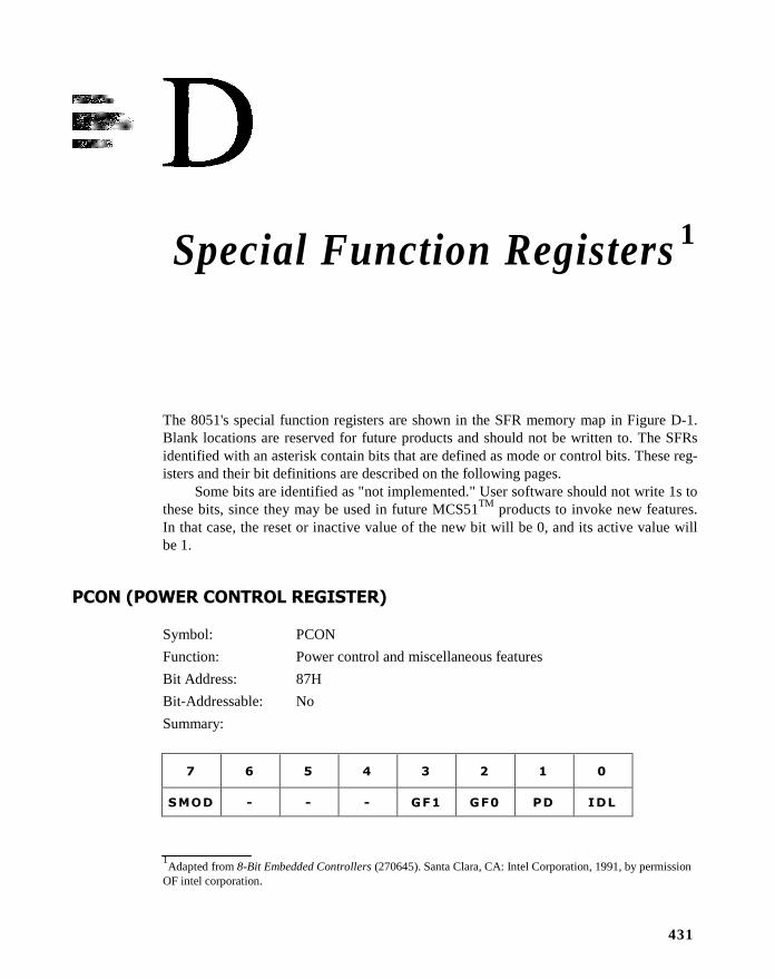
Special Function Registers 1
The 8051's special function registers are shown in the SFR memory map in Figure D-1.Blank locations are reserved for future products and should not be written to. The SFRsidentified with an asterisk contain bits that are defined as mode or control bits. These reg-isters and their bit definitions are described on the following pages.
Some bits are identified as "not implemented." User software should not write 1s tothese bits, since they may be used in future MCS51
TMproducts to invoke new features.
In that case, the reset or inactive value of the new bit will be 0, and its active value willbe 1.
PCON (POWER CONTROL REGISTER)
Symbol: PCON
Function: Power control and miscellaneous features
Bit Address: 87H
Bit-Addressable: No
Summary:
7 6 5 4 3 2 1 0
SMOD - - - GF1 GF0 PD IDL
1Adapted from 8-Bit Embedded Controllers (270645). Santa Clara, CA: Intel Corporation, 1991, by permission
OF intel corporation.
431

432 | APPENDIX D
Bit Definitions:Bit BitSymbol Description
SMOD Double baud rate. If timer 1 is used to generate baud rate and SMOD = 1,the baud rate is doubled when the serial port is used in modes 1, 2, or 3.
—Not implemented; reserved for future use.
—Not implemented; reserved for future use.
—Not implemented; reserved for future use.
GF1 General purpose flag bit 1.
GF0 General purpose flag bit 0.
PD Power down bit. Setting this bit activates power down operation in theCMOS version of the 8051.2
IDL Idle mode bit. Setting this bit activates idle mode operation in the CMOSversions of the 8051.2
8 Bytes
B
A C C
P S W *
T 2 C O N * RCAP2L RCAP2H T L 2 T H 2
I P *
P 3
I E *
P 2
S C O N * S B U F
P 1
T C O N * T M O D * T L 0 T L 1 T H 0 T H 1
F8
F0
E8
E0
D8
D0
C8
C0
B8
B0
A8
A0
98
90
88
80 P 0 S P D P L D P H P S W *
FF
F7
EF
E7
DF
D7
CF
C7
BF
B7
AF
A7
9F
97
8F
87
Bit *SFRs containing mode or controll bitsaddressable
FIGURE D-P3
Special function register memory map
21f 1s are writen to PD and IDL at the same time, PD take precedence

SPECIAL FUNCTION REGISTERS | 433
TCON (TIMER/COUNTER CONTROL REGISTER)
Symbol: TCON
Function: Timer/Counter Control
Bit Address: 88H
Bit-Addressable: Yes
Summary:
7 6 5 4 3 2 1 0
TF1 TR1 TF0 TR0 IE1 IT1 IE0 IT0
Bit Definitions:Bit BitSymbol Position Address Description
TF1 TCON.7 8FH Timer 1 overflow flag. Set by hardware whenthe timer/counter 1 overflow, cleared bysoftware or by hardware as processor vectorsto the interrupt service routine.
TR1 TCON.6 8EH Timer 1 run control bit. Set/cleared bysoftware to turn timer/counter 1 ON/OFF.
TF0 TCON.5 8DH Timer overflow flag. (See TF1)
TR0 TCON.4 8CH Timer 0 run control fit. (See TR1)
IE1 TCON.3 8BH External interrupt 1 edge flag. Set by hardwarewhen external interrupt edge is detected;cleared by hardware when interrupt isprocesse.
IT1 TCON.2 8AH Interrupt 1 type control bit. Set/cleared bysoftware to specify failing-edge/low-leveltriggered exteITll interrupt.
IE0 TCON.1 89H External interrupt 0 edge flag. (See IE1)
IT0 TCON.0 88H Interrupt 0 type control bit. (See IT1)
SCON (SERIAL CONTROL REGISTER)
Symbol: SCON
Function: Serial Port Control
Bit Address: 98H
Bit-Addressable: Yes

434 | APPENDIX D
TABLE D-1
SM0 SM1 Mode Description Baud Rate
0 0 0 Shift Register FOSC ¸ 12*0 1 1 8-bit UART Variable1 0 2 9-bit UART FOSC¸ 64 or FOSC ¸ 32
1 1 3 9SMt UART Variable
*FOSCis the oscillator frequency of the 8051 IC. Typically, this is derived from a crystal source of 12 MHz.
Summary:
7 6 5 4 3 2 1 0
SM0 SM1 SM2 REN TB8 RB8 TI RI
Bit DefinitionBit BitSymbol Position Address Description
SM0 SCON.7 9FH Serial port mode bit 0. (See Table D-l)
SM1 SCON.6 9EH Serial port mode bit 1. (See Table D-l)
SM2 SCON.5 9DH Serial port mode bit 2. Enable themultiprocessor communication feature inmodes 2 and 3. In mode 2 or 3, if SM2 is set to1, then RI will not be activated if the receivedninth data bit (RB8) is 0. In mode l, if SM2 =l, then RI will not be activated if a valid stopbit was not received. In mode 0, SM2 shouldbe 0.
REN SCON.4 9CH Receiver enable. Set/cleared by software toenable/disable reception.
TB8 SCON.3 9BH Transmit bit 8. The ninth bit that will betransmitted in modes 2 and 3. Set/cleared bysoftware.
RB8 SCON.2 9AH Receive bit 8. In modes 2 and 3, RB8 is theninth data bit that was received. In mode 1, ifSM2 = 0, RB8 is the stop bit that wasreceived. In mode 0, TB8 is not used.
TI SCON.1 99H
.
Transmit interrupt. Set by hardware at the endof the eighth bit time in mode 0, or at thebeginning of the stop bit in the other modes.Must be cleared by software .
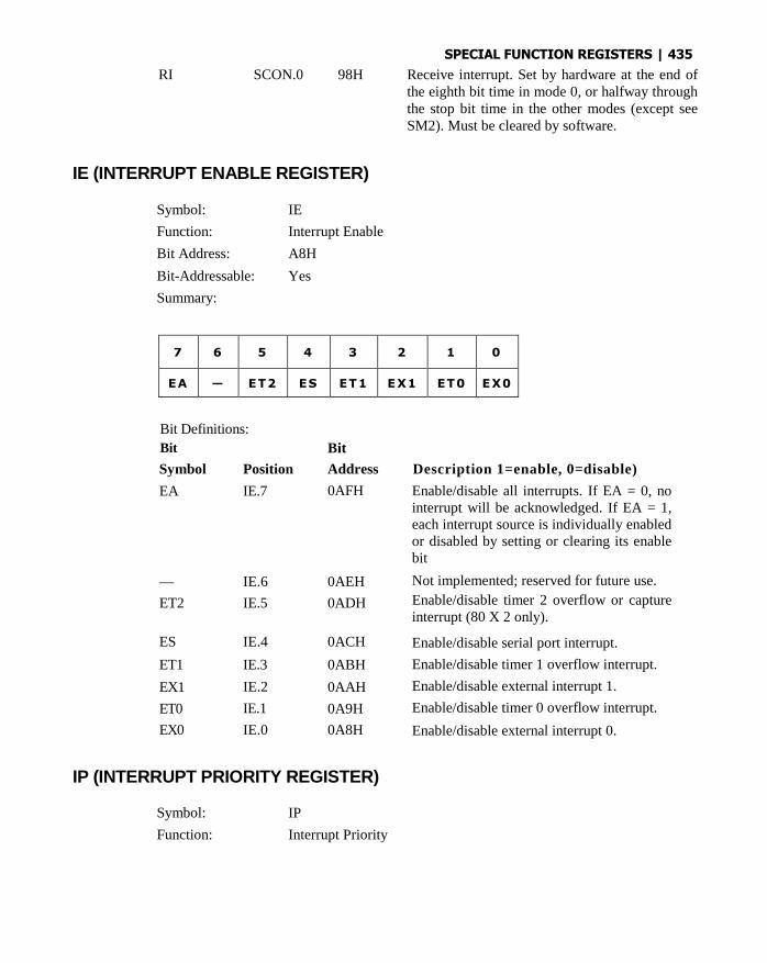
SPECIAL FUNCTION REGISTERS | 435
RI SCON.0 98H Receive interrupt. Set by hardware at the end ofthe eighth bit time in mode 0, or halfway throughthe stop bit time in the other modes (except seeSM2). Must be cleared by software.
IE (INTERRUPT ENABLE REGISTER)
Symbol: IE
Function: Interrupt Enable
Bit Address: A8H
Bit-Addressable: Yes
Summary:
7 6 5 4 3 2 1 0
EA — ET2 ES ET1 EX1 ET0 EX0
Bit Definitions:
Bit Bit
Symbol Position Address Description 1=enable, 0=disable)
EA IE.7 0AFH Enable/disable all interrupts. If EA = 0, nointerrupt will be acknowledged. If EA = 1,each interrupt source is individually enabledor disabled by setting or clearing its enablebit
— IE.6 0AEH Not implemented; reserved for future use.
ET2 IE.5 0ADH Enable/disable timer 2 overflow or captureinterrupt (80 X 2 only).
ES IE.4 0ACH Enable/disable serial port interrupt.
ET1 IE.3 0ABH Enable/disable timer 1 overflow interrupt.
EX1 IE.2 0AAH Enable/disable external interrupt 1.
ET0 IE.1 0A9H Enable/disable timer 0 overflow interrupt.
EX0 IE.0 0A8H Enable/disable external interrupt 0.
IP (INTERRUPT PRIORITY REGISTER)
Symbol: IP
Function: Interrupt Priority

436 | APPENDIX D
Bit Address: 0B8H
Bit-Addressable: Yes
Summary:
7 6 5 4 3 2 1 0
– – PT2 PS PT1 PX1 PT0 PX0
Bit Definitions:Bit Bit Description
Symbol Position Address (1 = high priority, 0 = low priority)
— P.7 0BFH Not implemented reserved for future use.
— IP.6 0BEH Not implemented; reserved for future use.
PT2 IP.5 0BDH Timer 2 interrupt priority level (80 X 2 only).
PS IP.4 0BCH Serial port interrupt priority level.
PT1 IP.3 0BBH Timer 1 interrupt priority level.
PX1 IP.2 0BAH External interrupt 1 priority level.
PT0 IP.1 0B9H Timer 0 interrupt priority level.
PX0 IP.0 0B8H External interrupt 0 priority level.
T2CON (TIMER/COUNTER 2 CONTROL REGISTER)
SyIP.H: T2CON
Function: Timer/Counter 2 Control
Bit Address: C8H
Bit-Addressable: Yes
Summary:
7 6 5 4 3 2 1 0
TF2 EXF2 RCLK TCLK EXEN2 TR2 C/T2 CP/RL2
Bit Definitions:Bit Bit
Symbol Position Address Description
TF2 T2CON.7 0CFH Timer 2 overflow flag. Set by hardware andcleared by software. TF2 cannot be set wheneither RCLK = 1 or TCLK = 1.
SPECIAL FUNCTION REGISTERS | 437
EXF2 T2CON.6 0CEHTimer 2 external flag. Set when either acapture or reload is caused by a negativetransition on T2EX and EXEN2 = 1. Whentimer 2 interrupt is enabled, EXF2 = 1 willcause the CPU to vector to the timer interruptservice routine. EXF2 must be cleared bysoftware.
RCLK T2CON.5 0CDH Receive clock. When set, causes the serial portto use timer 2 overflow pulses for its receiveclock in modes 1 and 3. RCLK = 0 causestimer 1 overflow to be used for the receiveclock.
TCLK T2CON.4 0CCH Transmit clock. When set, causes the serialport to use timer overflow pulses for itstransmit clock in modes 1 and 3. TCLK = 0causes timer 1 overflows to be used for thetransmit clock.
EXEN2 T2CON.3 0CBH Timer 2 external enable flag. When set, allowsa capture of reload to occur as a result ofnegative transition on T2EX if timer 2 is notbeing used to clock to serial port. EXEN2 = 0causes timer 2 to ignore events at T2EX.
TR2 T2CON.2 0CAH Timer 2 run bit. Software START/STOPcontrol for timer 2; A logic 1 starts the timer.
C/T2 T2CON.1 0C9H Counter/timer select for timer 2. 0 = internaltimer, 1 = external event counter (falling edgetriggered).
CP/RL2 T2CON.0 0C8H Capture/reload flag. When set captures willoccur on negative transitions at T2EXCPIRL2
EXEN2 = 1. When cleared, auto-reloads willoccur either with timer 2 overflows or onnegative transitions at T2EX when EXEN2 =1. When either RCLK = 1 or TCLK = 1, thisbit is ignored and the timer is forced toautoreload on timer 2 overflows.
PSW (PROGRAM STATUS WORD)
Symbol: PSW
Function: Program Status
Bit Address: 0D0H
Bit Addressable: Yes
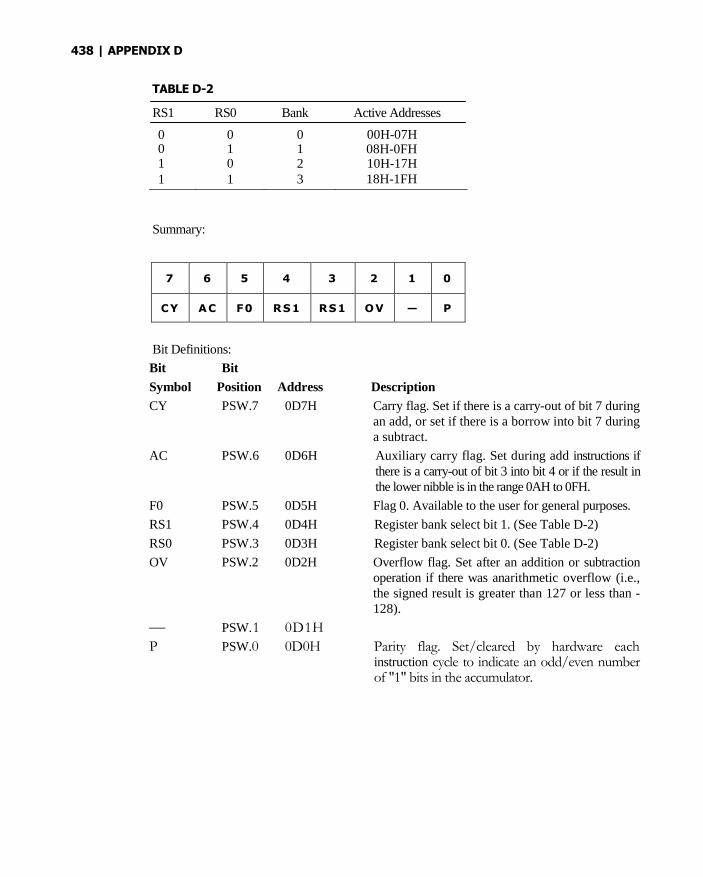
438 | APPENDIX D
TABLE D-2
RS1 RS0 Bank Active Addresses
0 0 0 00H-07H0 1 1 08H-0FH1 0 2 10H-17H1 1 3 18H-1FH
Summary:
7 6 5 4 3 2 1 0
CY AC F0 RS1 RS1 OV — P
Bit Definitions:
Bit Bit
Symbol Position Address Description
CY PSW.7 0D7H Carry flag. Set if there is a carry-out of bit 7 duringan add, or set if there is a borrow into bit 7 duringa subtract.
AC PSW.6 0D6H Auxiliary carry flag. Set during add instructions ifthere is a carry-out of bit 3 into bit 4 or if the result inthe lower nibble is in the range 0AH to 0FH.
F0 PSW.5 0D5H Flag 0. Available to the user for general purposes.
RS1 PSW.4 0D4H Register bank select bit 1. (See Table D-2)
RS0 PSW.3 0D3H Register bank select bit 0. (See Table D-2)
OV PSW.2 0D2H Overflow flag. Set after an addition or subtractionoperation if there was anarithmetic overflow (i.e.,the signed result is greater than 127 or less than -128).
— PSW.1 0D1H
P PSW.0 0D0H Parity flag. Set/cleared by hardware eachinstruction cycle to indicate an odd/even numberof "1" bits in the accumulator.

8051 Data Sheet 1
1Reprinted with permission of Intel Corporation from 8-Bit Embeded Controllers (270645). Santa Clara, CA:
Intel Corporation, 1991.
439
440 | APPENDIX E

8051 DATA SHEET | 441

442 | APPENDIX E

8051 DATA SHEET | 443

444 | APPENDIX E

8051 DATA SHEET | 445

446 | APPENDIX E

8051 DATA SHEET | 447

448 | APPENDIX E

8051 DATA SHEET | 449
450 | APPENDIX E

8051 DATA SHEET | 451

452 | APPENDIX E

8051 DATA SHEET | 453

454 | APPENDIX E
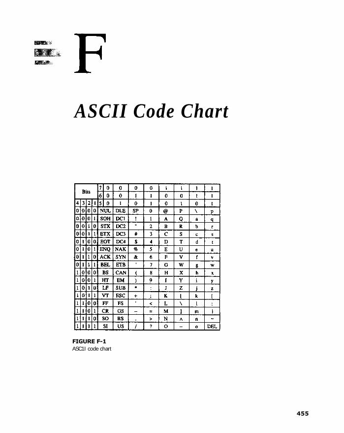
ASCII Code Chart
FIGURE F-1
ASC1I code chart
455

456 | APPENDIX E
MON51—An 8051 MonitorProgram
This appendix contains the listing for an 8051 monitor program (MON51) along with ageneral description of its design and operation. Many of the concepts in assembly lan-guage programming developed earlier in short examples (see Chapter 7) can be reinforcedby reviewing this appendix. The source and listing files for MON51 are contained on thediskette accompanying this text.
MON51 is a monitor program written for the 8051 microcontroller and, more speci-fically, for the SBC-51 single-board computer (see Chapter 11). We begin with adescription of the purpose of a monitor program and then give a summary of MON51commands. The overall operation of MON51 and some design details are also described.The final pages of this appendix contain listings of each assembled source file, the listingcreated by RL51, and a dump of MON51 in Intel hexadecimal format.
A monitor program is not an operating system. It is a small program with commands thatprovide a primitive level of system operation and user interaction. The major difference is thatoperating systems are found on larger computers with disk drives, while monitor programs arefound on small systems, such as the SBC-51, with a keyboard (or keypad) for input and a CRT(or LEDs) for output. Some single-board computers also provide mass storage using an audiocassette interface.
MON51 is an 8051 assembly language program approximately two kilobytes inlength. It was written on an Intel iPDS100 development system using an editor (CREDIT),a cross assembler (ASM51), and a linker/locator (RL51). Testing and debugging were per-formed using a hardware emulator (EMV51) connected to an Intel SDK-51TM single-board computer. It is worth mentioning that hardware emulators are such powerful toolsthat the first version of MON51 burned into EPROM was essentially "bug-free."
MON51 was developed using modular programming techniques. Ten source files wereused, including nine program files and one macro definition file. To keep the listing files rel-atively short for this appendix, the "create symbol table" option was switched off in each
457

458 | APPENDIX G
source file using the $NOSYMBOLS assembler control. (See MAIN.LST, line 4 on p. 466.)However, since the $DEBUG assembler control was also used, the listing file created by thelinker/locator, RL51, contains a complete, absolute symbol table for the entire program. Thelinker/locator absolute output was placed in V12 (for "version 12") and the listing file wasplaced in V12.M51. The OH (object-to-hex) utility was used to convert the absolute outputto an Intel hex file, V12.HEX, suitable for printing, downloading to a target system, orburning into EPROM. (Spaces have been inserted into the hex file to improve readability.)
The files appearing in this appendix are identified below.
File Page
ASM51 Listings
MAIN.LST 466
GETPAR.LST 470
IO.LST 473
CONVRT.LST 478
LOAD.LST 479
DUMP.LST 481
SFR.LST 484
IS.LST 488
SET.LST 489
Macro Definitions
MACROS.SRC 493
RL51 Listing
V12.M51 494
Hex File
V12.HEX 496
COMMANDS AND SPECIFICATIONS
MON51 uses the 8051's on-chip serial port for input/output. It requires an RS232C VDT ope-rating at 2400 baud with seven data bits, one stop bit, and odd parity. Command line editing ispossible using the BACKSPACE or DELETE keys to back up and correct mistakes. VT100escape sequences are used (see below).
The following four commands are supported:
DUMP dump the contents of a range of memory locations tothe console
SET examine single memory locations and set their contents to anew value
GO go to user program at a specified address
LOAD load an Intel hex-formatted file
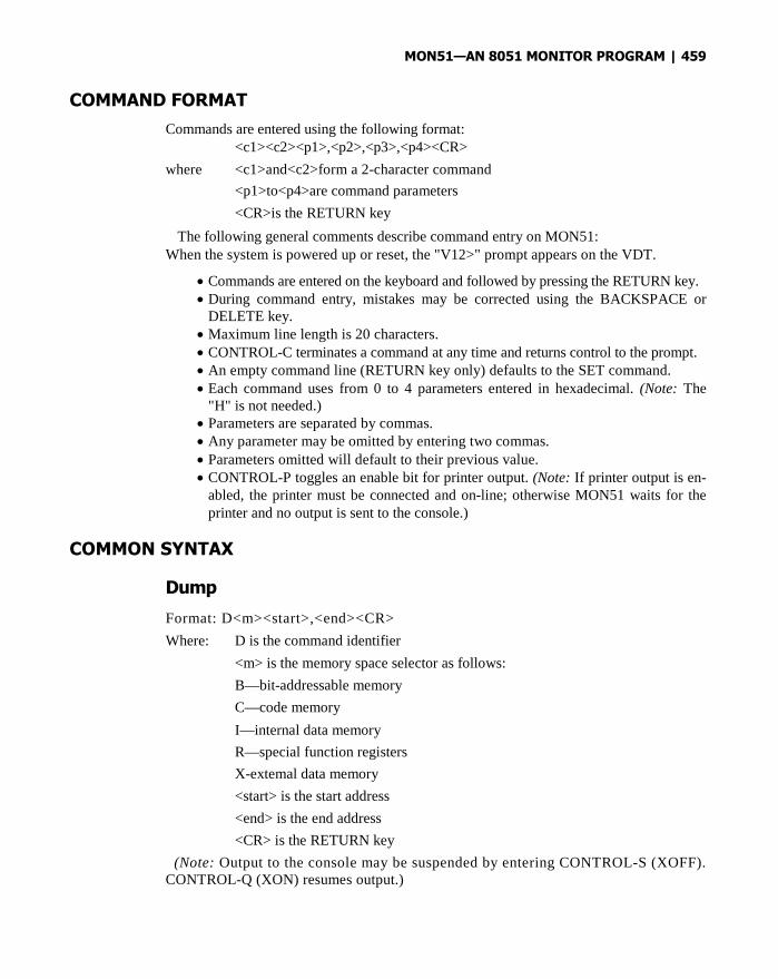
MON51—AN 8051 MONITOR PROGRAM | 459
COMMAND FORMAT
Commands are entered using the following format:<c1><c2><p1>,<p2>,<p3>,<p4><CR>
where <c1>and<c2>form a 2-character command
<p1>to<p4>are command parameters
<CR>is the RETURN key
The following general comments describe command entry on MON51:When the system is powered up or reset, the "V12>" prompt appears on the VDT.
Commands are entered on the keyboard and followed by pressing the RETURN key. During command entry, mistakes may be corrected using the BACKSPACE or
DELETE key. Maximum line length is 20 characters. CONTROL-C terminates a command at any time and returns control to the prompt. An empty command line (RETURN key only) defaults to the SET command. Each command uses from 0 to 4 parameters entered in hexadecimal. (Note: The
"H" is not needed.) Parameters are separated by commas. Any parameter may be omitted by entering two commas. Parameters omitted will default to their previous value. CONTROL-P toggles an enable bit for printer output. (Note: If printer output is en-
abled, the printer must be connected and on-line; otherwise MON51 waits for theprinter and no output is sent to the console.)
COMMON SYNTAX
Dump
Format: D<m><start>,<end><CR>
Where: D is the command identifier
<m> is the memory space selector as follows:
B—bit-addressable memory
C—code memory
I—internal data memory
R—special function registers
X-extemal data memory
<start> is the start address
<end> is the end address
<CR> is the RETURN key
(Note: Output to the console may be suspended by entering CONTROL-S (XOFF).CONTROL-Q (XON) resumes output.)
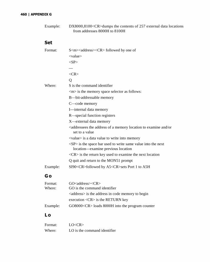
Example: DX8000,8100<CR>dumps the contents of 257 external data locationsfrom addresses 8000H to 8100H
Set
Format: S<m><address><CR> followed by one of
<value>
<SP>
—
<CR>
Q
Where: S is the command identifier
<m> is the memory space selector as follows:
B—bit-addressable memory
C—code memory
I—internal data memory
R—special function registers
X—external data memory
<addressees the address of a memory location to examine and/orset to a value
<value> is a data value to write into memory
<SP> is the space bar used to write same value into the nextlocation—examine previous location
<CR> is the return key used to examine the next location
Q quit and return to the MON51 prompt
Example: SI90<CR>followed by A5<CR>sets Port 1 to A5H
G o
Format: GO<address><CR>Where: GO is the command identifier
<address> is the address in code memory to begin
execution <CR> is the RETURN key
Example: GO8000<CR> loads 8000H into the program counter
L o
Format: LO<CR>
Where: LO is the command identifier
460 | APPENDIX G

MON51—AN 8051 MONITOR PROGRAM | 461
<CR>is the RETURN key
Example: LO<CR> The message "<host download to SBC-51>" appears.MON51 receives an Intel hex-formatted file at the serial port and writesthe bytes received into external data memory. When the transfer iscomplete, the message "EOF—file download OK" appears. Note: Usethe DUMP command to verify that the transfer was successful.
GENERAL OPERATION OF MON51
The general operation of MON51 is described by the following steps:
1. Initialize registers and memory locations.2. Send prompt to VDT display.3. Get a command line from VDT keyboard.4. Decode command.5. Execute command6. Go to step 2.
Although numerous subroutines and program modules participate in the overall opera-tion of MON51, the basic framework to implement the above steps is found in MAIN.LST.The instructions to initialize registers and memory locations (step 1) are lines 171 to 200 (seepp. 467-68). The prompt is sent to the VDT display in lines 201 and 202, and then a commandis inputted from the VDT keyboard in lines 203 and 204 (steps 3 and 4). The command is de-coded in lines 205 to 224. MON51 is designed to support 26 commands, one for each letter inthe alphabet. Only four are implemented, however, while the others are for future expansionor custom applications. Decoding the command entails (a) using the first character in the inputline buffer to look up the command's address from the table in lines 227 to 252, (b) placing thecommand's address on the stack (1 byte at a time), and (c) popping the address into the pro-gram counter using the RET instruction (line 225).
The code for the DUMP, SET, and LOAD commands is contained in separate files,while the code for the GO command is found in MAIN.LST in lines 268 to 274. Numeroussubroutines are used throughout MON51 and can be found in the various listings provided.
During command decoding, the subroutine GETPAR is called (line 224). This sub-routine gets parameters from the input line (which are stored in the line buffer as ASCIIcharacters) and converts them to binary, placing the results in internal RAM at four 16-bitlocations starting at the label PARMTR (see GETPAR.LST, line 58 on p. 471). These pa-rameters are needed by the commands DUMP, SET, and GO.
After each command is executed, control is passed back to MON51 at the labelGETCMD (line 200 in MAIN.LST) and the above steps are repeated. User programs may ter-minate, using the address of GETCMD (00BCH) as the destination of an LJMP instruction.
MON51 contains numerous comments, and each subroutine and file contains a com-ment block explaining the general operation of the section of code that follows. Readersinterested in understanding the intricacies of MON51 operation are directed to the listingfiles and comment lines for further details. In the following section, the overall design ofMON51 is discussed.

462 | APPENDIX G
THE DESIGN OF MON51
Developing an understanding of the "design" (as opposed to the operation) is also important,since MON51 incorporates—on a relatively large scale—many of the concepts developed ear-lier in brief examples. The following paragraphs elaborate on key design features that can beadopted in developing software for 8051-based designs. In a sense, then, the present appendixis like a case study—describing the design details of an existing 8051 software product.
Assembler controls, as mentioned in Chapter 7, are used primarily to control the for-mat and content of the listing files created by ASM51 and RL51. At the top of each of thenine program listings, several assembler controls appear. These were chosen primarily toproduce listing files suitable for reproduction in this appendix. Note in MAIN.LST, for ex-ample, that the control $NOLIST is used in line 6. This was used because line 7 (notlisted) contained the control $INCLUDE(MACROS.SRC), which directed ASM51 to thefile containing the macro definitions (pp. 493-94). Turning the "list" option off and on justbefore and after the $INCLUDE statement prevented ASM51 from needlessly putting themacro definitions into MAIN.LST.
Many of the assembler directives supported by ASM51 appear throughout theMON51 listing files. Recall (Section 7.5 Assembler Directives) that ASM51 supports fivecategories of directives:
Assembler state control Symbol definition Storage initialization/reservation Program linkage Segment selection
Examples from each of these categories appear in the listings.
Assembler State Control. The only assembler state control directives used in MON51 areEND and USING. The ORG directive was never used, since the code and data segmentswere designed to be relocatable with addresses established only at link-time.1 An instanceof USING can be found in GETPAR.LST, line 108 on p. 472.
Symbol Definitions. Many symbols are defined throughout MON51, as, for example, inMAIN.LST, lines 115 to 127 (pp. 466-67). Note in particular the definitions for EPROM,ONCHIP, and BITRAM. EPROM is defined as the name for a code segment. Similarly,ONCHEP is defined as the data segment and BITRAM is defined as the bit segment. All threeare, by definition, relocatable. Recall that the segment type "DATA" corresponds to the 8051on-chip data space accessible by direct addressing (00H to 7FH). All instructions in MON51go in the EPROM code segment, all on-chip data locations are defined in the ONCHIP datasegment, and all bit locations are defined in the BITRAM segment.
Storage Initialization/Reservation. The define byte directive (DB) is used throughoutMON51 to initialize code memory with byte constants. Usually, the definition is for ASCIIcharacter strings sent to the console as part of MON51 's normal operation. For example,the prompt characters for MON51 are defined in MAIN.LST on lines 288 and 289.
1The only exception to this is the absolute definition of the stack using the DSEG directive (see p. 469, line 288).

MON51—AN 8051 MONITOR PROGRAM | 463
Other definitions include the escape sequence sent to the console to back up the cursor.MON51 is designed to work with VT100 compatible terminals. If the BACKSPACE orDELETE key is pressed while you are entering a line, the escape sequence <ESC>0 [(or hexa-decimal bytes 1BH, 5BH, and 44H)] must be sent to the terminal. These bytes are defined as anull-terminated ASCII string (see IO.LST, line 144 on p. 475) using the DB directive. Oncethe code for the BACKSPACE or DELETE key is detected (see lines 17 and 18 on p. 473 andlines 133 and 135 on p. 475), the pointer to the input line buffer is decremented twice, and the"back-up cursor" escape sequence is sent to the console, using the output string (OUT-SIR)subroutine. (See lines 136 to 139 on p. 475.)
Storage locations are reserved using either the define storage (DS) or define bit(DBIT) directives. The first instance of a DS directive defines a 24-byte stack (see line288 in MAIN.LST) in an absolute data segment starting at address 08H in internal RAM.MON51 does not use register banks 1 to 3, so internal RAM addresses 08H to 1FH havebeen reserved for the stack. The default value of 07H for the stack pointer ensures that thefirst write to the stack is at address 08H. A 20-byte buffer for the command line isreserved at line 296 in MAIN.LST. Several bit locations are reserved in the BITRAM bitsegment at the end of MAIN.LST.
Program Linkage. The PUBLIC and EXTRN directives are used near the beginning ofmost source files. PUBLIC declares which symbols defined in a particular file are to bemade available for use in other source files. EXTRN declares which symbols are used in thecurrent source file but are defined in another source file. The NAME directive is not used inMON51; therefore, each file is a module with the file name serving as the module name.
Several of the files for MON51 hold the source code for subroutines used elsewhere.For example, IO.LST (pp. 473-78) contains the source code for the input/output subrou-tines INCHAR, OUTCHR, INLINE, OUTSTR, OUTHEX, and OUT2HX. These subrou-tines are all declared as "public" in line 26 (p. 473). Other files that use these subroutinesmust contain a statement declaring these symbols as external code address symbols (e.g.,MAIN,LST, line 108 on p. 466). Where these subroutines are called, the address for theLCALL or ACALL instruction is unknown by ASM51, so "F" appears in the listing file toindicate that linking/locating is required to "fix" the instruction. For example, inMAIN,LST the prompt is sent to the console in line 202, using ACALL OUTSTR. Thisinstruction appears in the listing as 1100H with an "F' beside it. The linker/locator, RL51,will determine the correct absolute address of the OUTSTR subroutines and fix theinstruction. In this example, since the addressing mode is absolute within the current 2Kpage, the fix substitutes 11 bits into the instruction—three bits in the upper byte and alleight bits in the lower byte.
Segment Selection. The segment selection directives are RSEG to select a relocatablesegment, and the five directives to select an absolute segment of a specified memory space(DSEG, BSEG, XSEG, CSEG, and ISEG). The RSEG is used at least once in each file tobegin the EPROM code segment (e.g., MAIN,LST, line 129, p. 467). Other instances ofRSEG appear as necessary to select the ONCHIP data segment (e.g., MAIN,LST, line295) or the BITRAM bit segment (e.g., MAIN,LST, line 306, p. 470). The only instanceof an absolute segment is the definition of the stack at absolute internal RAM address 08H(MAIN,LST, line 287, p. 469).

464 | APPENDIX G
OPTION JUMPERS
The SBC-51 has three jumpers on Port 1 that are read by software to evoke special features.MON51 reads these jumpers after a system reset and sets or clears corresponding bit locations(see MAIN.LST lines 171 to 176). Each jumper has a special purpose as outlined below.
Jumper Installed PurposeX3 NO normal execution
YES jump to 2000H upon reset
X4 NO interrupt jump table at 80xxH
YES interrupt jump table at 20xxH
X13 NO normal execution
YES software UART (see below)
Caution should be exercised when you are interfacing I/O circuitry to Port 1. If the attachedinterface presents a logic 0 to the corresponding pin during a system reset, this is interpretedby MON51 as if the jumper were installed, and the option listed above takes effect.
Reset Entry Point. Jumper X3 can be installed to force a jump to 2000H immediately aftera system reset (see MAIN.LST, line 199). This is useful in order to have both the MON51EPROM and a user EPROM installed simultaneously and to select which executes upon re-set. If, for example, the user program does not use a VDT, then it is inconvenient to powerup in "MON51 mode" just to enter GO2000H to evoke the user program. The installationof jumper X3 avoids the need for this.
Interrupt Jump Tables. Although MON51 does not use interrupts, user applications that co-exist with MON51 can adopt an interrupt-driven design. Since MON51 resides in EPROMstarting at address 0000H and since all interrupts vector to locations near the bottom of memory,a jump table was devised to allow user applications executing at other addresses to employinterrupts. Based on the default hardware configuration of the SBC-51, user applications gen-erally execute either in RAM starting at 8000H or in EPROM starting at 2000H. If a user ap-plication enables interrupts and subsequently an interrupt occurs and is accepted, the interruptvector address (i.e., entry point) is one of 0003H, 000BH, and 0013H, etc., depending on thesource of the interrupt (see Table 6-4). At each interrupt vector address in MON51, there is ashort instruction sequence that jumps to a location either in the user EPROM at 20xxH or inRAM at 80xxH, depending on whether or not jumper X4 is installed on the SBC-51 (seeMAIN.LST, lines 150 to 183). The correct entry point for each interrupt is listed below.
INTERRUPT ENTRY POINT
Interrupt Source X4 Installed X4 Not Installed
(default entry point) 2000H 8000HExternal 0 2003H 8003HTimer 0 2006H 8006HExternal 1 2009H 8009HTimer 1 200CH 800CHSerial Port 200FH 800FHTimer 2 2012H 8012H
MON51—AN 8051 MONITOR PROGRAM | 465
The entry points above are spaced three locations apart, leaving just enough room for anLJMP instruction to the interrupt service routine. If operation is from a 12 MHz crystal, 6µs is added to the interrupt latency because of the overhead of this scheme (due to the JNBand LJMP instructions in MON51 and the LJMP instruction in the user program). Ofcourse, if user applications do not use interrupts, programs may begin at 2000H or 8000Hand proceed through the above entry points.
For an example of a user application using interrupts that coexists with MON51, seethe MC14499 interface project in Chapter 11.
Software UART. When jumper X13 is installed, MON51 implements a software UARTfor serial input/output instead of using the 8051's on-chip serial port. This feature is usefulfor developing interfaces to serial devices other than the default terminal. Note that thebaud rate is 1200 if the software UART is used. The operation of the software UART isdescribed in IO.LST (p. 477, 11.219-278).
THE LINK MAP AND SYMBOL TABLE
One of the most important listings is that produced by the linker/locator, RL51. This list-ing, V12.M51 (pp. 494-96), contains a link map and symbol table. The link map shows thestarting address and length of the three relocatable segments used by MON51 (p. 495).The addresses are absolute at this stage, since the segments have been located by RL51based on the specifications provided in the invocation line (p. 494). The symbol tablegives the absolute values assigned to all relocatable symbols (as assigned by RL51 at link-time). It is partitioned alphabetically by module (i.e., file) in the order linked.
As an example, the absolute address of the OUTSTR subroutine is determined bylooking up OUTSTR in the IO module (p. 495-96). The address of OUTSTR in MON51version 12 is 0282H.
INTEL HEX FILE
The final listing is that produced by the OH (object-to-hex) conversion utility. The listingV12.HEX (pp. 496-98) contains the machine-language bytes of the MON51 program inIntel hexadecimal format. For example, the OUTSTR subroutine starts at address 0282H.On p. 497, the first three bytes of this subroutine appear as E4H, 93H, and 60H. Referringdirectly to the OUTSTR subroutine in the IO.LST confirms that these values are correct(see p. 476, 11.156-158).
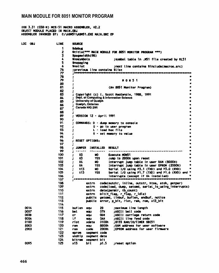
MAIN MODULE FOR 8051 MONITOR PROGRAM
466

467

468
469
470

471
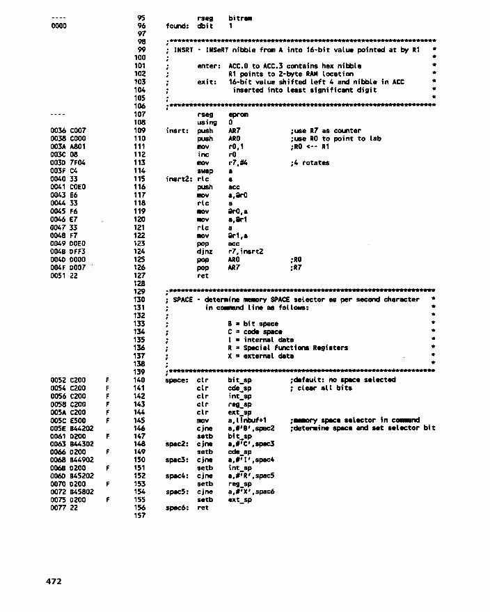
472
473
474

475

476
477

CONVERSION SUBROUTINES
478

479

480

481

482

483

READ AND WRITE SFRs
484

485

486
487

"IS" ROUTINES
488
489

490

491

492

493

V12.M51
494

495

V12.HEX
496

497
498 | APPENDIX G

A Guide to Keil'sµVISION2 IDE
INTRODUCTION
Keil's µVision2 Integrated Development Environment (IDE)1
is software that allows the8051 C programmer to edit, compile, run, and debug 8051 C programs. This appendixpresents a brief guide to using the µVision2 IDE.
THE µVISION2 WORKSPACE
When you double-click the µVision2 IDE, you will see a screen similar to the one shownin Figure H-1. The main windows that appear are the Workspace, the Edit window, and theOutput window.
The Workspace is a pane with three tabs that open different windows—Files, Regs,and Books. The Files window (see Figure H-2) allows you to manage the source code filesthat you want to include in your current project. Right-click the Simulator option and thenchoose "Select Device for Target 'Simulators" to indicate the target 8051 or derivativedevice for which you want to write a C program. To add a file to your project, simplyright-click the "Source Group 1" option and browse for the desired C file.
If you prefer to create a new program, then select New from the File menu and start key-ing the code for your program. When you have finished, save it as a C file and add it to yourproject. In Figure H-2, you can see that the sole file included in the project is test.c. Double-clicka file name to open it and it will display in the Edit window, as shown in Figure H-1.
COMPILING AND DEBUGGING
When you have finished editing your program, the next thing you want to do is compile it tosee if there are any compile errors. For this, you could select "Build target" from the Project
1An evaluation version is available for download at http://www.keil.com/demo/.
499

FIGURE H-1
µVision2 IDE
500
FIGURE H-2The Files window

A GUIDE TO KEIL'S µVISION2 IDE | 501
FIGURE H-3
Select "Build target" from the Project menu
menu (see Figure H-3). This will compile all recently updated files in your project. Alterna-tively, you could select "Translate ... " to compile only the C file you have currently high-lighted, or "Rebuild all target files" to compile all files in your project, regardless of whetheror not you have just updated them. The Output tab should display 0 errors.
Before downloading the compiled program into the ROM of your 8051, it is advis-able to test and debug it to determine if it executes as desired. Select "Start/Stop DebugSession" from the Debug menu (see Figure H-4). If you want to run the program frombeginning to the end, select "Go" from the Debug menu. Otherwise, if you would like toexecute one C statement at a time, select the "Step" option.
In the debugging session, as you are stepping through or running your program, youcan choose to view the status of registers by clicking on the Regs tab to open the Regswindow (see Figure H-5).
FIGURE H-4
Select "Start/Stop Debug Session" from the Debug menu

502|APPENDIXH
Figure H-5 shows the Regs windhighlighted. You can also view the memfrom the View menu. The Memory winlower-right corner of the screen. Figurecations starting from 0103H. If you womemory, then click in the text box to threfers to internal data memory and 0000Keying C instead of D enables you to vlocation, simply double-click the locatFigure H-7) and key the new value intoues in decimal or in hex, using standard
Viewing the contents and status ofthem from the Peripherals menu. As an etents of Port 0.
FIGURE H-6
Memory window
FIGURE H-5
ow with the stack pointer (SP) and its contentsory contents by selecting "Memory Window"
dow (see Figure H-6) normally appears at theH-6 shows the contents of external memory lo-uld rather look at the contents of internal datae right of "Address:" and key D:0000, where Dspecify the starting location you want to view.
iew code memory. To modify a certain memoryion and choose "Modify Memory at ... " (seethe edit box that appears. You can enter the val-C notation.the on-chip peripherals is also easy by selectingxample, Figure H-8 shows how to view the con-
Regs window
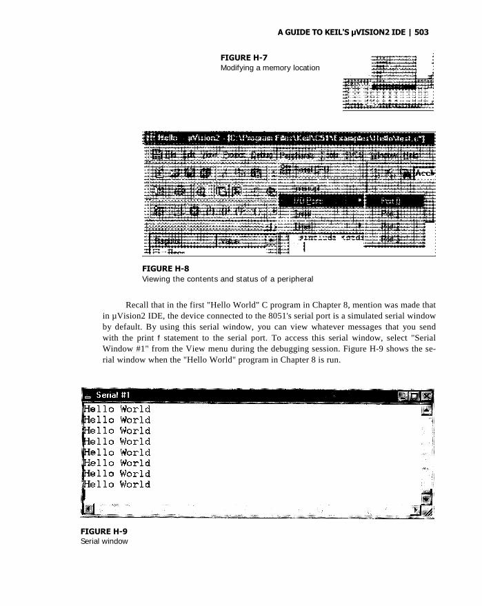
A GUIDE TO KEIL'S µVISION2 IDE | 503
FIGURE H-8
Viewing the contents and status of a peripheral
Recall that in the first "Hello World" C program in Chapter 8, mention was made that
in µVision2 IDE, the device connected to the 8051's serial port is a simulated serial window
by default. By using this serial window, you can view whatever messages that you send
with the print f statement to the serial port. To access this serial window, select "Serial
Window #1" from the View menu during the debugging session. Figure H-9 shows the se-
rial window when the "Hello World" program in Chapter 8 is run.
FIGURE H-7
Modifying a memory location
FIGURE H-9Serial window

5
04 | APPENDIX HIn the section on timers in Chapter 8, you learned that you could direct the µVision2'sC compiler to disassemble your C programs into assembly language. To view the correspon-ding assembly language version of your program, select "Disassembly Window" from theView menu. Figure H-10 shows the disassembly of our "Hello World" program, with theoriginal C statements shown right above their corresponding assembly language instructions.
FIGURE H-10Disassembly window
FIGURE H-11Options for the target
A GUIDE TO KEIL'S µVISION2 IDE | 505
FIGURE H-12
Output options tab
Once you are satisfied with the debugging and simulation of your program, you candirect the µVision2 to generate the machine code as a HEX file. Right-click the Simulatoroption in the Files window, and then select "Options for Target ... " (see Figure H-11).Click the Output tab and check the "Create HEX File" option (see Figure H-12).
With this option selected, the next time you build the target, a HEX file would becreated in the same directory as your C file. You can then download this HEX file intoROM, and the 8051 will be ready to execute the program the moment you switch it on.

A Guide to the 8052Simulator
INTRODUCTION
The 8052 Simulator for Windows is software that simulates the entire operation of the8051 or 8052 microcontroller, plus all its registers, internal RAM locations, I/O ports,timers, serial ports, and interrupts. During the initial stages of developing an 8051—or8052—based system, you can test the assembled or compiled program entirely insoftware with the help of this simulator, without having to worry about the actualhardware. This appendix provides a brief guide to using the 8052 Simulator.
The 8052 Simulator
The main window of the 8052 Simulator is as shown in Figure I-1. The first thing you needto do is to load an already assembled or compiled program that has been saved in Intel HEXformat. Most 8051 assemblers and compilers have an option to save the assembled or com-piled output in this format. Figure 1-2 shows how this is done by selecting the "Open Intel-Standard File" from the File menu and then browsing for the Intel HEX file.
The loaded program is now ready to be tested. First, you can choose to view variouscomponents of the 8051, such as the internal RAM, I/O ports, special function registers(SFRs), and timers. Select each of these from the View menu, as shown in Figure 1-3.
Figure 1-4 shows the Internal Memory (RAM) window that was selected from theView menu. All the rows of the first column represent the addresses of 16 memory locations,the contents of which are displayed in the 16 columns on the right. For example, the first rowconsists of the internal memory locations 00H to 0FH, and as can be seen in Figure 1-4, thecontent of each is 0. To modify any location, click it and then key the new value in hexa-decimal form. Alternatively, you can choose to check (set) or leave unchecked (clear) any ofthe 8 bits in that location.
'By Vault Information Services, 8174 S. Holly PMB 272, Littleton, CO 80122, U.S.A.E-mail: [email protected].
507
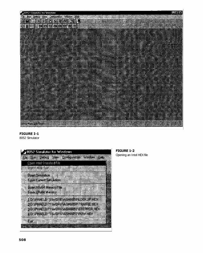
F
8
5
IGURE I-1
052 Simulator
FIGURE 1-2
Opening an Intel HEX file
08

F
V
IGURE 1-4
iewing internal RAM
FIGURE 1-3
Viewing internal components of the
8051
509

5
10|APPENDIXIYou can choose to view the contents of up to 64K of external RAM from the sameView menu. Selecting "I/O Ports" from the View menu displays the Ports window (seeFigure 1-5), which is straightforward enough. The contents of all four I/O ports are shownin the figure. You can modify their contents using a process similar to that used to modifyinternal or external RAM.
Figure 1-6 shows the SFRs window, which displays the contents of all the SFRs inthe 8051's upper 128 internal RAM locations. Again, their contents can be modified by
FIGURE 1-6
Viewing SFRs
FIGURE 1-5
Viewing I/O ports

F
V
A GUIDE TO THE 8052 SIMULATOR | 511
clicking on the white boxes and then keying the new value in hex. Notice also that at thebottom of the SFRs window is the "Current Instruction" section. The box at left in thisarea shows the location in code memory of the next instruction to be executed while theright box shows that next instruction.
Also available for viewing is the Timers window (see Figure I-7), which shows thecontents of the TCON and TMOD registers as well as the timer count values of Timers 0,1, and 2 (for the 8052).
The serial port is also simulated by a terminal window (see Figure I-8) that displayswhatever characters are sent to the serial port. The full version of the 8052 Simulator also
IGURE 1-8
iewing the terminal window
FIGURE 1-7
Viewing timers

512 | APPENDIX I
supports connection of the 8051's serial port to the computer's COMM/serial port, so thatany data sent to or received from the 8051 serial port would be sent to or received fromthe computer's COMM/serial port.
Let's assume that the HEX file corresponding to the assembly language program inFigure 11-33 has been loaded. This is the program for the pedestrian traffic light system.To test execute the program, first display the relevant windows using the View menu. Forexample, you could display the internal RAM, I/O ports, and SFRs windows. Next, youcould choose to run the entire program right by choosing the "Execute Program" from theRun menu. You can stop the program execution at any time by selecting "Stop" from thesame menu. Alternatively, you could execute each instruction one by one by choosing"Single Step" from the Debug menu, or use F8, the shortcut key for the option that willallow you to run each step separately.
For example, the first instruction in the traffic light program is to jump to MAIN.Press F8 once to execute this instruction, and then press F8 again to execute the next in-struction, which is to move the value 81H into the IE register (see Figure 1-9). You willsee that the content displayed in the IE register's is now 81H. In a similar way, you canstep through the rest of the program one step at a time, checking the suitable SFR, internalRAM locations, I/O ports, or timers to see if they are changed as expected. To reset theprogram to the beginning, simply choose "Reset Program" from the Run menu.
At any time during the program execution or as you execute it one step at a time, youcan select "Program Analysis" from the View menu to display useful information such asthe number of instructions so far executed and how many machine cycles have been used.
FIGURE 1-9Checking the program one step at a time

A GUIDE TO THE 8052 SIMULATOR | 513
There is also an Execution History area in the Program Analysis window that lists all pre-viously executed instructions (see Figure I-10.)
An added feature in the 8052 Simulator is the 4 x 5 keypad simulator (see Figure I-11).This simulates the functions of a 4 x 5 keypad, similar to the 4 x 4 hexadecimal keypad dis-cussed in Chapter 11. You can customize the names of any key simply by right-clicking thekey you want to change and then keying the new name.
FIGURE 1-10The Program Analysis window
FIGURE I-11The keypad simulator

514 | APPENDIX I
You can also customize which port pins will be used to connect the rows andcolumns by selecting "Keypad Configuration" from the Configuration menu. This isshown in Figure 1-12.
FIGURE 1-12
The Keypad Configuration window

The Advanced EncryptionStandard
INTRODUCTION
As the 8051 is used more and more in smart cards, where the security of information is almostalways important, it is most often used to execute software or hardware implementations ofencryption methods. The current standard for encryption is the Advanced Encryption Standard(AES), a recent and secure method that was officially adopted in 2000 by the U.S. NationalInstitute of Standards & Technology (NIST) for encrypting confidential, nonclassifiedinformation in the United States. It is expected that the AES will replace the Data EncryptionStandard in ATM cards, smart cards, online transactions, and other security-relatedapplications. Therefore, the study of the 8051 would not be complete without a discussion ofthe AES. This appendix is intended to acquaint the reader on how the AES works so that youwill understand how the AES can be implemented with the 8051.
BLOCK ENCRYPTION
These days, messages and information are digitally stored in files in the computer in terms ofbits of 1 s and 0s. These messages vary in size from a few bytes to a few hundredmegabytes. For that reason, current encryption methods specify a standard input block size,typically 128 bits. A message that is to be encrypted first must be broken down into blocksof 128 bits, and then each block is encrypted. The encrypted blocks are then concatenated toform the encrypted message. See Figure J-1 for an illustration of this process.
HOW THE AES WORKS
For the purpose of describing the AES, its designers represented the 128-bit input block asa 4 x 4 array of bytes. An element of this array is denoted by a1, where i and j are the rowand column indices respectively, numbered from 0 to 3, as shown in Figure J-2.
5 1 5
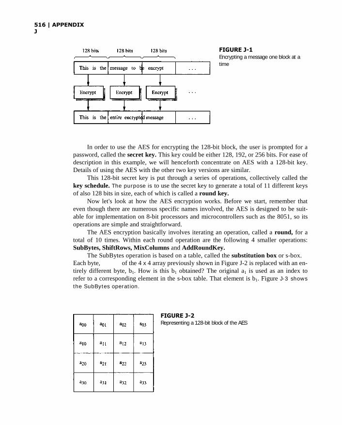
516 | APPENDJ
pdD
ko
eao
tS
Etrt
IX
In order to use the AES for encrypting the 128-bit block, the user is prompted for aassword, called the secret key. This key could be either 128, 192, or 256 bits. For ease ofescription in this example, we will henceforth concentrate on AES with a 128-bit key.etails of using the AES with the other two key versions are similar.
This 128-bit secret key is put through a series of operations, collectively called theey schedule. The purpose is to use the secret key to generate a total of 11 different keysf also 128 bits in size, each of which is called a round key.
Now let's look at how the AES encryption works. Before we start, remember thatven though there are numerous specific names involved, the AES is designed to be suit-ble for implementation on 8-bit processors and microcontrollers such as the 8051, so itsperations are simple and straightforward.
The AES encryption basically involves iterating an operation, called a round, for aotal of 10 times. Within each round operation are the following 4 smaller operations:ubBytes, ShiftRows, MixColumns and AddRoundKey.
The SubBytes operation is based on a table, called the substitution box or s-box.ach byte, of the 4 x 4 array previously shown in Figure J-2 is replaced with an en-
irely different byte, b1. How is this b1 obtained? The original a1 is used as an index toefer to a corresponding element in the s-box table. That element is b1. Figure J-3 shows
he SubBytes operation.
FIGURE J-1Encrypting a message one block at a
time
FIGURE J-2Representing a 128-bit block of the AES
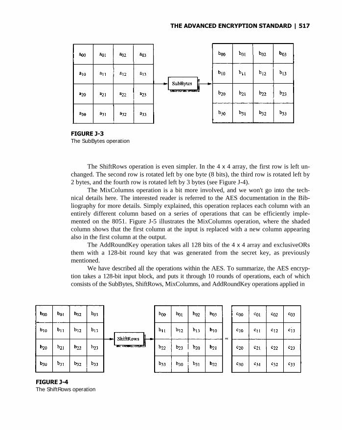
THE ADVANCED ENCRYPTION STANDARD | 517
FIGURE J-3The SubBytes operation
The ShiftRows operation is even simpler. In the 4 x 4 array, the first row is left un-changed. The second row is rotated left by one byte (8 bits), the third row is rotated left by2 bytes, and the fourth row is rotated left by 3 bytes (see Figure J-4).
The MixColumns operation is a bit more involved, and we won't go into the tech-nical details here. The interested reader is referred to the AES documentation in the Bib-liography for more details. Simply explained, this operation replaces each column with anentirely different column based on a series of operations that can be efficiently imple-mented on the 8051. Figure J-5 illustrates the MixColumns operation, where the shadedcolumn shows that the first column at the input is replaced with a new column appearingalso in the first column at the output.
The AddRoundKey operation takes all 128 bits of the 4 x 4 array and exclusiveORsthem with a 128-bit round key that was generated from the secret key, as previouslymentioned.
We have described all the operations within the AES. To summarize, the AES encryp-tion takes a 128-bit input block, and puts it through 10 rounds of operations, each of whichconsists of the SubBytes, ShiftRows, MixColumns, and AddRoundKey operations applied in
FIGURE J-4The ShiftRows operation

518 | APPENDIX J
FIGURE J-5
The MixColumns operation
sequence. However, an extra AddRoundKey operation is added prior to the first round,and the MixColumns operation is omitted from the last round. These slight adjustmentsare design choices to make encryption and decryption similar in structure. This similarityis desired because it allows for more compact hardware and software implementations. Anillustration of the entire AES encryption process is shown in Figure J-6.
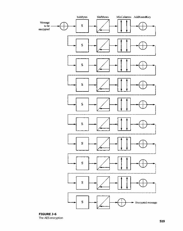
FIGURE J-6The AES encryption
519
Sources of 8051Development Products
Allen Systems, 2151 Fairfax Road, Columbus, OH 43221
Product: FX-31 8052-BASIC SBC
Description: 8052 single-board computer with built-in BASIC interpreter
Product: CA-51
Description: 8051 cross assembler
Host Computer: IBM PC and compatibles
Product: DP-31/535
Description: Single-board computer based on Siemens 80535 CPU
Applied Microsystems Corp., 5020 148th Ave. N. E., P.O. Box
97002, Redmond, WA 98073-9702
Product: EC7000
Description: 8051 microcontroller emulator
Host Computer: IBM PC and compatibles
Aprotek, 1071-A Avenida Acaso, Camarillo, CA 93010
Product: PA8751
Description: 8751 programming adapter
Features: Adapts 8751 EPROM microcontrollers to any EPROMprogrammer as a 2732
521

522 | APPENDIX K
Avoset Systems, Inc., 804 South State St.,
Dover, DE 19901
Product: XASM51
Description: 8051 cross assembler
Host Computer: IBM PC and compatibles
Product: AVSIM51
Description: 8051 family simulator
Host Computer: IBM PC and compatibles
Binary Technology, Inc., B.O. Box 67, Meridan,
NH 03770
Product: SIBEC-Il
Description: 8052 single-board computer with built-in BASICinterpreter
Cybernetic Micro Systems, Inc., P.O. Box 3000,
San Gregorio, CA 94074
Product: CYS8051
Description: 8051 cross assembler
Host Computer: IBM PC and compatibles
Features: Does not generate relocatable modules
Product: SIM8051
Description: 8051 simulator
Host Computer: IBM PC and compatibles
Product: CYS8051
Description: EPROM programmer for 8751
Interface: RS232 serial
Decmation, Inc., 3375 Scott Blvd., Suite #236,
Santa Clara, CA 95054
Product: ASM51, PLM51 SIM51, etc.
Description: 8051 development software
Host Computer: VAX, PDP-11, IBM PC and compatibles
SOURCES OF 8051 DEVELOPMENT PRODUCTS | 523
HiTech Equipment Corp., 9560 Black Mountain Road,
San Diego, CA 92126
Product: 8051 SIM
Description: 8051 simulator
Host Computer: IBM PC/XT or Z80 CP/M microcomputers
Huntsville Microsystems, Inc., P.O. Box 12415, 4040
South Memorial Parkway, Huntsville, AL 35802
Product: SBE-31, HMI-200-8051
Description: 8051 emulator
Interface: Serial
Host Computer: Various computers with CP/M or MS-DOS operating system
Keil Software, Inc., 1501 10" Street, Suite 110,
Plano, TX 75074
Product: µVision2 IDE
Description: 8051 C compiler and debugger
Host Computer: IBM PC and compatibles
Logical Systems Corp., 6184 Beall Station, Syracuse,
NY 13217
Product: UPA8751
Description: 8751 programming adaptor
Features: Adapts 8751 to 2732 socket for installation into any EPROMprogrammer
Product: SIM51
Description: 8051 simulator and debugger
Host Computer: IBM PC (MS-DOS, CP/M) and compatibles
Micromint, Inc., 4 Park Street, Vernon, CT 06066
Product: BCC52
Description: 8052 single-board computer with built-in interpreter
524 | APPENDIX K
Nohau Corp., 51 East Campbell Ave., Suite 107E, Campbell,
CA 95008
Product: EMV51-PC
Description: 8051 emulator
Host Computer: IBM PC and compatibles
Relational Memory Systems, Inc., P.O. Box 6719, San Jose,
CA 95150
Product: ASM51 RLINK, RLOC, GLIB, OBJCON
Description: 8051 software development tools
Host Computer: IBM PC and compatibles
Scientific Engineering Laboratories, Inc., 104 Charles Street,
Suite 143, Boston, MA 02114
Product: XPAS51
Description: 8051 PASCAL cross compiler
Host Computer: IBM PC and compatibles
Single Board Systems, B.O. Box 3788, Salem, OR 97306
Product: SBS-52
Description: 8052 single-board computer with built-in BASIC interpreter
Software Development Systems, Inc., 3110 Woodstock Drive,
Downers Grove, IL 60515
Product: A51
Description: 8051 cross assembler
Host Computer: Various systems running MS-DOS, Xenix, or Unix
Universal Cross Assemblers, P.O. Box 384, Bedford,
Nova Scotia B4A 2X3, Canada
Product: CROSS-16
Description: 8051 cross assembler
Host Computer: IBM PC and compatibles

SOURCES OF 8051 DEVELOPMENT PRODUCTS | 525
URDA, Inc., 1811 Jancey St., Suite #200, Pittsburgh, PA 15206
Product: SBC-51
Description: PC board version of SBC-51 described in this text
Z-World, 2065 Martin Ave. #110, Santa Clara, CA 95050
Product: IBM PC co-processor
Description: Co-processor plugs into PC or PC/AT; runs Intel's ISIS operatingsystem and software development tools
IC MANUFACTURERS
The following companies are manufacturers and/or developers of the 8051 and derivative ICs.Intel Corp., 3065 Bowers Avenue, Santa Clara, CA 95051Siemens Components, Inc., 2191 Laurelwood Road, Santa Clara, CA 95054Signetics/Philips, 811 East Argues Ave., Sunnyvale, CA 94088-3409Advanced Micro Devices, Inc., 901 Thompson Place, P.O. Box 3453, Sunnyvale,
CA 94088-3453Fujitsu Microelectronics, Inc., 3320 Scott Blvd., Santa Clara, CA 95054-3197

526 | BIBLIOGRAPHY

ARTICLES
Ball, S. Embedded debugging tricks. Circuit Cellar (1995, September): 20-23.Boyet, H., and R. Katz. The 8051 one-chip microcomputer. Byte (1981, December):
288-311.Cantrell, T. Audio processor chips for the masses. Circuit Cellar (1995, November):
70-76.Cantrell, T. Chip on patrol. Circuit Cellar (1995, June): 64-71.Cantrell, T. Plan '251 for outer space!: Intel's 8xC251SB. Circuit Cellar (1995, March):
72-77.Cantrell, T. UFO alert. Circuit Cellar (1995, January): 100-107.Cheung, H. DRAM on an 8031: It's not as hard as you'd think. Circuit Cellar (1994,
September): 24-31.Ciarcia, S. Build the BASIC-52 computer/controller. Byte (1985, August): 105-117.Ciarcia, S. Build a gray-scale video digitizer—Part 1: Display/receiver. Byte (1987,
May): 95-106.Ciarcia, S. Build a gray-scale video digitizer—Part 2: Byte (1987, June): 129-138.Ciarcia, S. Build an intelligent serial EPROM programmer. Byte (1986, October):
103-119.Ciarcia, S. Build a trainable infrared master controller. Byte (1987, March): 113-123.Ciarcia, S. Why microcontrollers?—Part 1. Byte (1988, August): 239-245.Ciarcia, S. Why microcontrollers?—Part 2. Byte (1988, September): 303-323.Collier, M., and F. Gweme. Preventing the ultimate blow: A portable checking unit for
8751s. Circuit Cellar (1994, September): 48-43.Dinwiddle, G. An 8031 in-circuit emulator. Byte (1986, July): 181-194.Dybowski, J. Atmel's AT29C2051 flash-based microcontroller. Circuit Cellar (1995,
February): 76-80.Dybowski, J. Beef up the 8052 with the DS87C520. Circuit Cellar, no. 52 (1994,
November): 76-82.Dybowski, J. Embedded development. Circuit Cellar (1995, March): 78-84.Messick, P., and J. Battle. Build a MIDI input for your Casio SK-1 Keyboard (1987,
August): 34-40.Natarajan, K. S., and C. Eswarn Design of a CCITT V.22 modem. Microprocessors and
Microsystems 12(9) (1988, November): 532-535.
527
528 | BIBLIOGRAPHY
National Institute of Standards and Technology (NIST). Advanced Encryption Standard,Federal Information Processing Standard (FIPS) 197. (2002). Online:http://csrc.nist.gov/encryption/aes.
Schenker, J. Controller chip cuts keyboard redesign to weeks. Electronics 61(2) (1988,January 21): 42E-42F.
Vaidya, D. M. Microsystem design with the 8052-BASIC microcontroller.Microprocessors and Microsystems 9(8) (1985, October): 405-411.
Vaidya, D. M. Software development for the 8052-BASIC microcontroller.
Microprocessors and Microsystems 9(10) (1985, December): 481-485.Wallace, H. No emulator? Try a one-wire debugger. Circuit Cellar (1995, January):
20-23.
Warner, W. Use a single-chip microprocessor as the heart of your positioncontroller EDN (1988, Sept. 1) 161-168.
Yeskey, D. In-circuit 8051 emulator is a tool for the masses. Electronic Design (1988,January 7): 202.
BOOKS
8-bit Embedded Controllers (270645). Santa Clara, CA: Intel, 1991.Ayala, K. J. The 8051 Microcontroller: Architecture, Programming, and Applications.
New York: West, 1991.
Barnett, R. H. The 8051 Family of Microcontrollers. New Jersey: Prentice Hall, 1995.Boyet, H., and R. Katz. The 8051: Programming Interfacing Applications. New York:
MTI Publications, 1981.
Cx51 Compiler: Optimizing C Compiler and Library Reference for Classic and Extended8051 Microcontrollers. Keil Software, 2001.
Getting Started with µVision2 and the C51 Microcontroller Development Tools. KeilSoftware, 2001.
Mazidi, M. A., and J. G. Mazidi. The 8051 Microcontroller and Embedded Systems.New Jersey: Prentice Hall, 2000.
MCS-51 Macro Assembler User's Guide (9800937-03). Santa Clara, CA: Intel, 1983.Schultz, T. C and the 8051: Hardware, Modular Programming, and Multitasking.
New Jersey: Prentice Hall, 1998.Schneier, B. Applied Cryptography: Protocols, Algorithms, and Source Code in C.
New York: John Wiley & Sons, 1996.Stallings, W. Cryptography and Network Security: Principles and Practice. New Jersey:
Prentice Hall, 1999.Stewart, J. W., and K. X. Miao. The 8051 Microcontroller: Hardware, Software and
Interfacing. New Jersey: Prentice Hall, 1999.Yeralan, S., and A. Ahluwalia. Programming and Interfacing the 8051 Microcontroller.
Massachusetts: Prentice Hall, 1995.

1 kHz square wave, example, 99,206-207
3-wire communication, 3034-step stepper motor, 3117-segment LED display, interface to,
267-273,323-3258-bit auto-reload mode, 928-bit shift register, 113-1158-bit UART, with variable baud rate,
115-1178-step stepper motor, 3119-bit UART, 11710kHz square wave, example, 98-99,
206-20713-bit timer mode, 9116-bit timer mode, 92,9474HC165, 28675HC165, 287-28880C31BH 228031
external access (EA), 21summary of memory space, 24-25
8032,19enhancements, 41-43external access (EA), 21
8051block diagram of, 19configuration of, 260-263driving, from TTL oscillator, 22-23external access (EA), 21features of, 17-22illus., 2NAND operation using, 13-15pinouts, 18-22sources for development products,
521-525summary of on-chip data memory, 24,
26-27See also MCS-51
8051 C language
advantages and disadvantages of,191-192
as alternative to assembly languageprogramming, 191
arrays, 198-199compilers, 192-193data types, 193-196examples of, 204-214functions, 202-204memory types and models, 197-198pointers, 199-202structures, 199
8051 C programming style, 243-2458051 data sheet, 439-4538051 derivatives
high-speed microcontrollers, 378-379introduction, 377MCS-l51 and MCS-251, 377microcontrollers with ADCs and
DACs, 378microcontrollers with flash memory
and NVRAM, 377-378network microcontrollers, 379secure microcontrollers, 379
8051 monitor program (MON51), 259,457-498
command format, 459commands and specifications, 458common syntax, 459-461conversion subroutines, 478-479design on, 462-463dump memory to console, 481-484general operation of, 461get parameters from input line,
470-473Go, 460input/output routines, 473-478Intel HEX file, 465"IS" routines, 488-489link map and symbol table, 465
Lo, 460-461load Intel HEX file, 479-481macro.src, 493-494main module for, 466-470option jumpers, 464-465overview, 457-458read and write special register
functions (SFRs), 484-487Set, 460set memory to value, 489-493V12.HEX 496-498V12.M51,494-496
8052enhancements, 41-43external access (EA), 21port 1,19
8052 simulator, 507-514check program, 512-513introduction, 507-508Keypad Configuration window, 514keypad simulator, 513open Intel HEX file, 508Program Analysis window, 513view internal components of 8051,
509view internal RAM, 509view I/O ports, 510view special function registers
(SFRs), 510-511view terminal window, 511-512view timers, 511
8052 timer 2,105-1068085,218086,218088,218255,285-291,336-337
Absolute addressing, 57-58 AbsoluteCall instructions (ACALL),
75-76,385-386
529

530 | INDEX
Absolute code segment, 171-173Absolute jump, 73,76,158-159,389Absolute segments, selecting, 171-173AC. See Auxiliary carry flag (AC)ACALL. See Absolute Call instructions
(ACALL)Actuator, 8ADC. See Analog-to-digital converter
(ADC)ADC0804, 300-302ADD, 63,386-387ADD A, 386-387ADDC. See Add with carry (ADDC)Address bus
defined, 3,6multiplexing, and data bus, 36-37
Address decoding, 40-41Addressing modes
absolute addressing, 57-58direct addressing, 52-53immediate addressing, 54-55indexed addressing, 59indirect addressing, 53-54long addressing, 58-59register addressing, 50-52relative addressing, 55-57
Address latch enable (ALE), 21,35-36AddRoundKey, 516-519Add with carry (ADDC), 63,387-388Advanced Encryption Standard (AES)
block encryption, 515defined, 375illustration of process, 519introduction, 515working, 515-519
Advanced Micro Devices, Inc., 525AES. See Advanced Encryption
Standard (AES)AGAIN label, 238AHEAD label, 238AJMP. See Absolute jumpALE. See Address latch enable (ALE)Allen Systems, 521ALU. See Arithmetic and logic unit
(ALU)Analog input, 300-302,342-344Analog output, 296-300,342-344Analog-to-digital converter (ADC), 378AND, 64,71-72ANDed, 26ANDing, 12ANL, 389-391ANL C, 391Apple Macintosh, 9
Applications, 10-12Application software, 8-9Applied Microsystems Corp., 521Aprotek, 521Archival storage, 7ARCNET token ring network protocol,
379Arithmetic and logic unit (ALU), 4Arithmetic instructions, 59-64Arithmetic operators, 161,235Array, 198-199,244ASCII codes, 142-143,155,160,455ASCII table, for decimal digits, 198-199ASM51
assembler controls supported by,173-175
macro processing facility (MPL),183-188
Assembler, defined, 151-152Assembler controls, 155,173-175Assembler directives
assembler state control, 164-165program linkage, 169-171segment selection, 171-173storage initialization/reservation,
166-169symbol definition, 165-166
Assembler operationASM51 152-153pass one, 153pass two, 153-155
Assembler state control, 164-165Assembler symbols, special, 157Assemble-time error, 249Assemble-time expression evaluation,
160-163Assembly language program, 152Assembly language programming
8051 C language as alternative to, 191assembler controls, 173assembler directives, 164-173assembler operation, 152-155assemble-time expression evaluation,
160-163comments, 238-239format, 155-160labels, 237-238linker operation, 173-176linking relocatable segments and
modules, 176-183macros, 183-188overview, 151-152program organization, 243saving registers on stack, 239
use of equates, 239-240 useof subroutines, 240-242See also Structured programming
Assignment operators, 235-236Asynchronous format, 111-112,115AT89C15SND1C, 378AT89C15SND2C, 378ATM. See Automatic Teller Machine
(ATM)Atmel, 378-379"At" sign (@), 157,235ATWebSEG-32, 379Authentication, 372Auto-decrement modes, 11 Auto-increment, 11Automatic Teller Machine (ATM),372 Auto-reload mode, 105-106Auxiliary carry flag (AC), 30-31Avoset Systems, Inc., 522
Background interrupt level, 131-132BACK label, 237Base-level interrupt, 131-132Basic input/output system (BIOS), 8Baud rate, 111Baud rate generation, 87,106Baud rate summary, 122Binary-coded decimal (BCD), 30,63Binary data, convert voltage to, 8Binary Technology, Inc., 522BIOS. See Basic input/output system
(BIOS)Bit address, 158Bit-addressable internal data memory
(bdata), 166,197,202Bit-addressable RAM, 26-27Bit data type, 193-195Bit testing, 73Bitwise logical operators, 235-236Block encryption, 515Boolean accumulator, 30Boolean instructions, 71-73Boolean operations, 64Boolean variable instruction, 60Bootstrap loader, 8Breakpoint, 249B register, 32Built-in interrupt system, 10Bus, defined, 6. See also Address bus;
Control bus; Data busBUSY, 34Buzzer interface, example, 100-101,
207-208Bytes, 11
INDEX | 531
C, 151. See also 8051 C language; 8051C programming style
CAD. See Computer-aided (CAD)software
Caesar, Julius, 351Caesar cipher, 351,372Calculator, student project, 363-365CALL instructions, 73-76,158-160. See
also Absolute call instructions(ACALL); LCALL
CAN. See Controller Area Network(CAN)
Capture mode, 106Carriage return (CR), 239-240Carry flag, 29-30CASE statement, 230-234,237Cathode-ray tube (CRT), 7CD-ROM. See Compact-disc read-only
memory (CD-ROM)Central environment, 255-256Central processing unit (CPU), 3-5Centronics parallel interface, 294-296,
340-341Character output using interrupts,
example, 142-143,211-212Character strings, 160Character test, example, 228-230Choice structure, 220
CASE statement, 230-231GOTO statement, 234IF/THEN/ELSE statement, 228-230
Ciphertext, 350CJNE instruction, 77-78,185,392-394Clear Accumulator, 394Clear bit (CLR bit), 394-395Cleared, 26Clear to send (CTS), 291CLOCK, 7Clock cycle, 23-24Clocking, serial port, 116Clocking sources, 92-93CLR bit. See Clear bit (CLR bit)Code, 172,197Code address, 158-159CODE directive, 166Code memory (code), 166,197Code segment, 243Command language, 9Commands, 255-257Comment blocks, 237Comment field, 156-157Comments, 155,238-239,243Commodore Amiga, 9Compact-disc read-only memory
(CD-ROM), 7
Compact memory, 198Compare accumulator instruction, 185Compare and Jump if Not Equal. See
CJNECompiler, 192-193Complement Accumulator, 395Complement bit, 395-396Computer, defined, 3Computer-aided (CAD) software, 250Computer system, defined, 3COM20051 379Condition, 221Conditional jumps, 77-78,238Confidentiality, 372Constant definitions, 245Control bus, 3,6Control flow operations, 187-188Controller Area Network (CAN), 379Control/monitor device, 7-8CPL A, 395CPL bit, 395-396CPU. See Central processing unit (CPU)Cross assembler, 152Cross-compiler, 251CRT. See Cathode-ray tube (CRT)Cryptographic technique, 372CTS. See Clear to send (CTS)Cybernetic Micro Systems, Inc., 522
DA A. See Decimal adjust accumulator(DA A)
DAC. See Digital-to-analog converter(DAC)
"Dancing with bits," 66Data, defined, 6. See also Internal data
memory (data)Data address, 158Data bus, 3,6,36-37Data directives (DBs or DWs), 153,243Data Encryption Standard (DES), 372,
515Data pointer (DPTR), 33-34,9402Data segment, 243Data transfer instructions, 59
external RAM, 68-69internal RAM, 66-68look-up tables, 69-70
DB-9, 291DB-25, 291, 294DBIT directive, 168D2 by Motorola, 1Debugger, 249Debugging, 248DEC byte, 398-399
Decimal adjust accumulator (DA A),30-31,63,396-397
Decision block, 218Decmation, Inc., 522Decrement, 398-399Decrement and Jump if Not
Zero (DJNZ), 77,399-401Decryption, 350
Define byte (DB) directive, 168-169 Defines, 244Define storage (DS) directive, 166-167Define word (DW) directive, 169DES. See Data Encryption Standard
(DES)Development cycle
defined, 247-248detailed steps in, 252flowchart for, 248hardware development, 249-251software development, 248-249
Development environment, 256Dictionary attack, 375Digital signature, 372Digital-to-analog converter (DAC),
296-300,378DIP switch, 277Direct access memory (DMA), 6Direct addressing, 52-53Directives. See individual directivesDirectly addressable internal data
memory (data), 197,201-202Disk interface, 10DJNZ See Decrement and Jump if Not
Zero (DJNZ)DMA. See Direct access memory
(DMA)Double words, 11DPTR. See Data pointer (DPTR)DS. See Reserve memory directive (DS)DS89C420, 379DS5000 378-379DS5240, 379DS162O
command set, 303configuration/status register, 306interface to, 345-346software for interface, 304-306
EA. See External access (EA)ECHO.LST, 177-182Elevator system, student project, 355-358 Encryption, 350-351,372. See also
Advanced Encryption Standard(AES)

532 | INDEX
END directive, 164English alphabet, 351Environments, 255-257EPROM. See Erasable Programmable
Read-Only Memory (EPROM)Equate directive (EQU), 153,166Equates, 239-240Erasable Programmable Read-Only
Memory (EPROM), 2,20-21,37-38,172,254-255
Ethernet, 379Event. See InterruptsEvent counting, 87-88,93Exchange Accumulator with byte
variable, 427-428Exchange Digit (XCHD), 428Exclusive OR, 64EXF2. See External input flag (EXF2)EXIT subroutine, 241EXORing bits, 12Expression example, 163External access (EA), 21External code memory, accessing, 37-38External data address space, 172External data memory (xdata), 166,197,
201-202External input flag (EXF2), 134External interrupt, 143-148External memory
accessing, 38-41accessing external code memory,
36-41address decoding, 40-41multiplexing address bus and data
bus, 36-37overlapping external code and data
spaces, 41External RAM, 68-69EXTRN directive, 170
Factorial operation (!), 84Factory mask process, 254-255Fetching, 4-5,37-38Fields, 155-157. See also entries for
individual fieldsFilename suffix, 251Firmware, 13,254Flag, 87Flag flip-flop, 87Flash memory, 377-378flowcharts, 218Foreground (base-level) interrupt,
131-132"Forward references," 155
Frequencies, producing exact, 102-105Fujitsu Microelectronics, Inc., 525Full duplex, 111,117-118,125-126Function definitions, 245Function prototypes, 245Functions
defined, 202example of, 203parameter passing, 203return values, 204use of, in 8051 C programming style,
244Furnace controller, example, 144-145,
212-213
General controls, 173General-purpose RAM, 24-26GND. See Ground(GND) GOTO statement,234 Ground (GND), 291G6RN, 307-310
Hardwaredefined, 3versus software, 8-9
Hardware architecture, 10-12Hardware development, 249-251. See
also Development cycleHardware emulator, 253Hexadecimal keypad interface, 265-267,
319-323HEX records, 253-254High-speed microcontrollers, 378-379Hilech Equipment Corp., 523Home security system, student project,
353-355"Housekeeping" chores, 8Human interface, 7Huntsville Microsystems, Inc., 523
IBM, 8-9IC. See Integrated circuit (IC)IC manufacturers, 525IDE. See µVision2 Integrated
Development Environment(IDE)
Idle mode, 35IE. See Interrupt enable register (IE)IF/THEN/ELSE statement, 228-230,237Immediate addressing, 54-55Immediate data, 157-158INC, 401INC DPTR, 402In-circuit emulator, 253
Includes, 245Increment, 401-402Increment Data Pointer, 402Indentation, 219Indexed addressing, 59Indirect address, 53-54,157,236Indirect internal data, 172Indirectly addressable internal data
memory (idata), 166,197,202Initializing serial port, 123,208INLINE subroutine, 238-239Input character subroutine, example,
125,209Input/output block, 218Input/output device (I/O device), 9
control/monitor device, 8human interface device, 7mass storage device, 7
Input/output expansion8255,282-294,336-337shift registers, 282,285-286,333-336
Input/output program, example of,176-177
Input/output subroutines, 8-9Instruction decode and control unit, 4Instruction opcode, 4-5Instruction register (IR), 4Instructions
compensating for overhead due to,103-105
definitions, 385-430See also Assembler directives
Instruction set, 4addressing modes, 50-59 features, 10-12instruction types, 59-78 overview, 49
Instruction typesarithmetic, 59-64Boolean instructions, 71-73 datatransfer instructions, 59,66-70logical instructions, 59,64-66program branching instructions, 73-78 See also entries for individual types
Integrated circuit (IC), 1,5,9. See alsoRandom access memory(RAM); Read-only memory(ROM)
Integrity, 372Intel Corporation, 1-2,173,431,525Intel hexadecimal format, 253-254Intel HEX file, 508Interface circuit, defined, 3 Inter-Integrated Circuit, 379

INDEX | 533
Internal data, 172Internal data memory (data), 166,197,
201-202Internal RAM, 24,66-68Interrupt circuitry, 10-11Interrupt-driven system, 131,249Interrupt enable register (IE), 35,
132-133,435Interrupt flag, 119Interrupt flag bits, 134Interrupt handler, 131Interrupt latency, 149Interrupt level, 131-132Interrupt priority register (IP), 35,
133-134,435-436Interrupts, 75-77
character output using, 211-212enabling and disabling, 132-133example, 131-132external, 143-148furnace controller, example, 212-213intrusion warning system, example,
213-214loudspeaker using, 146-148memory organization when using, 138organization, 132-135overview, 131-132polling sequence, 134-135processing, 136program design using, 137-139serial port, 142-143square wave using timer example, 210timer, 139-141two square waves using timer
example, 210-211Interrupt service routine (ISR), 76,131,
137-139,249Interrupt timings, 148-149Interrupt vector, 136Interval timing, 87-88,92-93INTR line, 244Intrusion warning system, example,
145-148,213-214Invoking commands, 255-257I/O device. See Input/output device (I/O
device)IO.LST 178-183I/O port structure, 22-23IP. See Interrupt priority register (IP)IR. See Instruction register (IR)IR. See Interrupt service routine (IS)
JBC bit, 403-404JC rel, 404
JMP@A+DPTR, 404-405JMP mnemonic generic, 159JNB bit,rel, 405JNC instruction, 78JNC rel, 406JNZ instruction, 77,406-407Joystick, 7Jump if accumulator Not Zero, 406-407Jump if accumulator Zero, 407Jump if Bit Not set, 405Jump if Bit set and Clear bit, 403-404Jump if Carry is set, 404Jump if Carry not set, 406Jump indirect, 404-405Jumps, 158-160,238. See also entries
for individual jumpsJump tables, 74-75JZ instruction, 77JZ rel, 407
Keil Software, Inc., 192-193,204,523Keyboard, 7Keypad interface, software for, 268-
269. See also 7-segment LEDdisplay, interface to
Key schedule, 516Keyword, 219KIM-1, 1
Label, 237-238Label field, 155-157Large interrupt service routine, 138-139Large memory, 198Large-scale integrated (LSI) chips, 8LCALL instruction, 75-76,407-408LIB51 251Librarian, 251Light pen, 7Line feed (LF), 240Linkage operation, 173-176Linker, 151-152Linker operation, 176Link/locator, 173Liquid crystal display (LCD), interface
to, 273-276,325-327$LIST directive, 300Listing file, 155LJMP. See Long jump (LJMP)Load Data Pointer with a 16-bit
constant, 413Local label, 186-187Location counter, 153Logical-AND for bit variables, 391Logical-AND for byte variables, 389-391
Logical Exclusive-OR for byte variables(XRL), 428-430
Logical instructions, 59,64-66Logical operations. See Boolean
instructionsLogical operators, 161Logical-OR for bit variable, 419Logical-OR for byte variable, 417-418Logical Systems Corp., 523Logic gate program, flowchart for, 14-15Long addressing, 58-59Long Call to subroutine, 407-408Long interval instruction, 96-102Long jump (LJMP), 73,76,158-159,
273,408Look-up tables, 69-70LOOP label, 237Loop structure, 220
REPEAT/UNTIL statement, 226search subroutine, 226-228SUM subroutine, 222-224WHILE/DO structure, 221-222,
224-225Loudspeaker, 7
interface to, 276-279,327-329interface using interrupts, 146-148
LSI. See Large-scale integrated (LSI)chips
MAA. See Modulo ArithmeticAccelerator (MAA)
MAC. See Message authentication code(MAC)
Machine cycle, 23-24Machine language, 151Machine language program, 152Macro processing facility (MPL),
183-188Macros, 183
advantages in using, 184-185control flow operations, 187-188 example of, 184local labels, 186-187parameter passing, 185-186repeat operations, 187
Mainframe computer, 9—l0Main function, 245Mass storage, 7Maxim, 379Maxim Integrated Product, 378MC14499, interface to, 270-272MCS-48, 1MCS-51 2, 377
absolute maximum ratings, 444A.C. characteristic, 445-446

534 | INDEX
MCS-51 Continuedblock diagram, 441comparison of different versions,
17-18,24connections, 442design considerations, 443EPROM characteristics, 451-453external clock drive, 450external data memory read cyle, 448external data memory write cycle, 448external program memory read cycle,
447features, 440hardware architecture, 17-43instruction set, 49-85oscillator characteristics, 443PIN descriptions, 441-443serial port timing, shift register mode,
449See also 8051; 8051 data sheet
MCS-151, 378-379 MCS-251 377-379 Med iuminterval inst ruct ion , 96-102Memory
external, 36-41semiconductor, 5-6small, medium, and large, 198types for 8051 C language, 197
Memory map, 173-175,289Memory models, for 8051 C language,
198Memory organization
general-purpose RAM, 24-26register banks, 27-28when interrupts are used, 138
Message authentication code (MAC), 372Microcomputer system, block diagram
of, 3,11Microcontroller(s)
with ADCs and DACs, 378defined, 1-2with flash memory and NVRAM,
377-378high-speed, 378-379illus., implementation of simple logic
operation, 14market needs and technology, 12-13microprocessor versus, 10-12network, 379power, size, and complexity of, 2secure, 379speed, 13-15
Micromint, Inc., 523Micromouse, student project, 366-369
Microphone, 7Microprocessor, 9
versus microcontroller, 10-12new concepts, 12-13
Minicomputer, 9-10MixColumns, 516-519Mnemonic field, 155-156Mnemonics, 151MOD operator, 161Modular programming, 173,363Module, defined, 152Module name, 171Modulo Arithmetic Accelerator (MAA),
379MON51 See 8051 monitor program
(MON51)Monitor program. See 8051 monitor
program (MON51)MORE label, 237MOS Technology, 1Most significant bit (MSB), 92Motorola, 1Mouse, 7MOV DPTR,#data16, 413Move bit variable, 412-413Move byte variable, 409-412Move code byte or constant byte,
413-414Move External, 414-416MOVX instruction, 38-39MPL. See Macro processing facility
(MPL)MSB. See Most significant bit (MSB)Multiple, 416Multiprecision arithmetic, 64Multiprocessor communications,
119-120µVision2 Integrated Development
Environment (IDE), 499-505compiling and debugging, 499-505Disassembly window, 504File window, 500introduction, 499Memory window, 502Output options tab, 505Regs window, 502Serial window, 503workspace for, 499
NAME directive, 171NAND, 13-15,72National Institute of Standards &
Technology (NIST), 515National Semiconductor Corp., 300-302
Nested subroutine, 84,239Network microcontrollers, 379Nibbles, 11Ninth data bit, 118NIST. See National Institute of
Standards & Technology (NIST)Nohau Corp., 524Nonvolatile RAM (NVRAM) interface,
277-282,329-332No Operation (NOP), 416-417NOR operator, 72NOT operator, 64,72,161Number bases, 160Number sign (#), 54NVRAM, 377-378
Object file, 155OE. See Output Enable (OE)Off-page connector, 218ONCHIP, 172On-chip oscillator input, 22-23One pass assembler, 153One-Time Programmable (OTP) ROM,
377Online storage, 7"On the fly," 96Opcode fetch cycle, bus activity for, 5Opcodes, 21,37-38Operand field, 155-157Operating system software, 8-9Operator precedence, 163,236Optical disc, 7OR, 64,71-72Order, 219ORed, 26ORG directive, 164,172ORing, 12Oscillator, 22Oscillator clock cycle, 23-24Output character (OUTCHR) subroutine,
123-124,209,240-241Output Enable (OE), 20OUTSTR subroutine, 240-242OV. See Overflow flag (OV)Overflow flag (OV)
defined, 31-32timer modes and, 90-92
Overhead, compensating for, due toinstructions, 103-105
P. See Parity bit (P)Paged external data memory (pdata),
197,202Parallel interface, 10-11

INDEX | 535
Parameter passing, 185-186,203-204Parity bit (P)
adding, 118-119defined, 32
Pascal, 151Pass one, 153Pass two, 153-155PC, 8-9PC. See Program counter (PC)PCBs. See Printed circuit boards (PCBs)PCON. See Power control register
(PCON)Pedestrian traffic light system, 307-310,
347-348Peripheral device, defined, 3Personal Identification Numbers (PINs),
372Philips, 379PINs. See Personal Identification
Numbers (PINE)PKI. See Public-key infrastructure (PM)Pointers
defined, 199different ways of accessing data,
200-201memory type, 201typed, 201-202untyped, 202use of, in 8051 C programming style,
244Pointer's memory type, 201-202Polling sequence, 134-135Polyalphabetic cipher, 372Pop from stack (POP direct), 419-420Port 0,18Port 1, 18-19Port 2,19Port 3,19-21Port register, 34Pound sign (#), 157-158Power connection, 22Power control register (PCON), 35-36,
431-432Power down mode, 35-36PPI. See Programmable peripheral
interface (PPI)Precedence operation, 236Pre-defined process (subroutine), 218Printed circuit boards (PCBs), 250Printer, 7Process box, 218Program branching instruction, 60
conditional jumps, 77-78interrupts, 75-77
jump tables, 74-75subroutines, 75-77variations of, 73
Program counter (PC), 4Program development
commands and environment, 255-257development cycle, 247-251integration and verification, 251-255
Program flow arrow, 218Program linkage, 169-171Programmable peripheral interface
(PPI), 285. See also 8255Program organization, in 8051 C
programming style, 245Program(s)
defined, 5-6,152types of, 8-9See also Software
Program status word (PSW), 437-438auxiliary carry flag (AC), 30-31carry flag, 29-30overflow flag (OV), 31-32parity bit (P), 32register bank select bits, 31
Program Store Enable (PSEN), 20-21,35-37
Program terminator, 218PROM programmer, 378PSEN. See Program Store Enable
(PSEN)Pseudo code, 217-218
examples of subroutines, 234-235suggested syntax for, 235-237
PSW. See Program status word (PSW)PUBLIC directive, 169-170Public-key infrastructure (PKI), 379Pulse wave generation, example, 97,
205-206PUSH instruction, 67Push onto stack (PUSH direct)
instruction, 420
RAM. See Random access memory(RAM)
RAM data location, 243. See also Datasegment
Random access memory (RAM), 8bit-addressable, 26-27defined, 3external, 68-69features, 5-6general purpose, 24-26internal, 66-68testing software, 253-254
RCA, 1READ, 7READ control signal, 4"Read latch," 22Read-modify-write operation, 22Read-only memory (ROM), 8
defined, 3features, 5-6
"Read pin," 22Receive buffering, 111Receive data (RXD), 291Receive interrupt flag (RI), 119,134Receiver enable (REN), 118Reg51.h 195-196Register addressing, 50-52Register bank, 27-28Register bank select bits, 31Registers, 4,239Relational expression, 221Relational Memory Systems, Inc., 524Relational operator, 162,235-236Relative addressing, 55-57Relative jump, 158-159Relays, interface to, 306-310,346-348Relocatable object file, 155Relocatable object models, 251Relocatable segment (RSEG), 171,
176-183REN. See Receiver enable (REN)Repeat operations, 187REPEAT/UNTIL statement, 226,237Reserved words, 235Reserve memory directive (DS), 153Reset (RST), 22,43Resident, 255RET instruction, 76,420-421RETI instruction, 76,138-139,421-422RETURN, 240Return from interrupt, 421-422Return from subroutine, 420-421Return values, 204RI. See Receive interrupt flag (RI)RL51 173, 251RL A, 422RLC A, 422-423Robot, 366. See also entries for
individual robotsROM. See Read-only memory (ROM)Rotate Accumulator, 423Rotate Accumulator Left, 422Rotate Accumulator Left through the
Carry flag, 422-423Rotate Accumulator Right through Carry
flag, 423

536 | INDEX
Rotor, 310-311Round, 516Round key, 516Round-off errors, example, 103,127RR A, 423RRC A, 423RSEG. See Relocatable segment (RSEG)RSEG directive, 165-166RS232 (IEA-232) serial interface,
294-294,337-340RST. See Reset (RST)Run-time error, 249RXD. See Receive data (RXD)
SAB80C515A,378 378SBC. See Single-board computer (SBC)SBC-51, 259
components and parts, 260printed circuit board version of, 266schematic design for, 260-265
Sbit data type, 193-195SBUF. See Serial port buffer register
(SBUF)Schottky TTL, 22Scientific Engineering Laboratories,
Inc., 524SCON. See Serial port control register
(SCON)SDK-85, 1Search subroutine, 226-228Secret key, 516Secure microcontrollers, 379Segment, defined, 152SEGMENT directive, 165Segment selection directives, 171-173Semiconductor memory, 5-6SEND label, 238Sensors, 8,303-306,344-346Serial communication, 111-112,
117-118Serial data buffer (SBUF), 34Serial interface, 10-11Serial port
block diagram of,112 clocking, 116initializing, 123,208input character subroutine, 209modes, 114output character subroutine, 209setting T1 flag, 116
Serial port baud rate baudrate summary, 122compensating for round-off errors
example, 127
default, 120-121full duplex operation example,
125-126initializing serial port example, 123input character subroutine example,
125output character subroutine example,
123-124using timer 1 as baud rate clock,
121-127"wait loop," 124
Serial port buffer register (SBUF),111-112
Serial port control register (SCON), 35,111,113,433-435
Serial port interrupts, 142-143Serial port operation
full duplex serial communication,117-118
initialization and accessing serial portregisters, 118-119
modes of, 113-117multiprocessor communications,
119-120serial communication, 111-112 serialport baud rates, 120-127 serial portbuffer register (SBUF), 112 serialport control register (SCON),
113Serial port receive timing, 115Serial port register, 34-35,118-119Serial port shift register mode, 115Serial port transmit timing, 114Set, 226SETB, 424Set Bit, 424SET directive, 166SFR. See Special function register (SFR)Sfr data type, 194-195Sfr16 data type, 194-195Shift register mode, 115Shift registers, 282,285-286,333-336ShiftRows, 516-517Short interval instruction, 96-102Short jump (SJMP), 73,424-425Siemens Corporation, 2,378Signetics/Philips, 525Simens Compponents, Inc., 525Simulator, 251-253Sine wave table, 297-300Single-board computer (SBC), 1,250Single Board Systems, 524Single-stepping, 249SJMP. See Short jump (SJMP)
SKIP label, 238Small interrupt service routine,
137-138Small memory, 198Smart card, 350,371-374Soccer-playing robot, 369-371Software
defined, 3,5designing, 249editing and translation, 249hardware versus, 8-9levels of, 9preliminary testing, 249See also Development cycle;
ProgramSoftware Development Systems, Inc.,
524Software simulation, 251-253SP. See Stack pointer (SP)Special assembler symbols, 157Special function register (SFR)
8051 instruction, 28accumulator, 28B register, 32data pointer (DPTR), 33-34interrupt enable register (1E), 35,435interrupt priority register (IP),
435-436memory map, 432port register, 34power control register (PCON),
35-36,431-432program status word (PSW), 29-32,
437-438serial port control register (SCON),
433-435serial port register, 34-35stack pointer (SP), 33timer, 88-89timer/counter control register
(TCON), 433timer/counter 2 control register
(T2CON), 436-437time register, 34
Special operator, 162Split timer mode, 92SQUARE subroutine, 70Square wave generation, example, 98Square wave using timer interrupts,
example, 139-141Stack, save registers on, 239Stack pointer (SP), 33Standard Microsystems, 379Start-up programs, 8-9
INDEX | 537
State, 23-24Statement block, 220
Stator, 310Stepper motor
configuration of stator windings of,
310half-step rotation of, 311interface to, 312,348-350rotating rotor of, 311
software for interface to, 313-315
Storage initialization/reservation, 166-169String replacement facility, 183. See also
Macros
Structure, 199Structured programming
8051 C programming style, 243-245advantages and disadvantages of,
219-220assembly language programming
style, 237-243choice, 220,228-234choice structure, 228-234
loops, 220-228overview, 217-219pseudo code syntax, 234-237statement block, 220
SUBB. See Subtract with borrow(SUBB)
SubBytes, 516-517
Subroutines, 75-77use of, 240-242use of registers within, 239
See also Interrupts and entries for
individual types of subroutinesSubtract with borrow (SUBB), 61-62,
425-426
SUM subroutine, 222-224Swap nibble within Accumulator (SWAP
A), 66,426-427
Symbol, 156. See also entries for
individual symbolsSymbol definition, 165-166
Symbol table, 153,173-175,183Synchronous format, 111-112,115Syntax error, 249
TCON. See Timer/counter controlregister (TCON)
TF2. See Timer overflow flag (TF2)TI. See Transmit interrupt flag (TI)Tic-tac-toe, student project, 358-363Timed intervals, 96-102Timer/counter control register (TCON),
34,89-90,93-94,433
Timer/counter 2 control register(T2CON), 42,102
Timer interrupts, 139-141Timer mode register (TMOD), 34,89Timer operation, 87-109
baud rate generation, 106
clocking sources, 92-93
8052 timer 2,105-106initializing and accessing timer
registers, 95-96
overview, 87-89producing exact frequencies, 102-105
short, medium, and long intervals,
96-102starting, stopping, and controlling
timers, 93-95timer control register (TCON), 89
timer mode register (TMOD), 34,89timer modes and overflow flag (OV),
90-92
Timer overflow flag (TF2), 134Timer register, 34,42,95-96
Timer(s)defined, 87-88example, 99-100,205
modes, 34,90-92reading "on the fly," 96
starting, stopping, and controlling,
93-95Timer special function registers, 88-89MOD. See Timer mode register
(TMOD)
Transient, 255Transistor-transistor logic (TTL), 15Transistor-transistor logic (TEL)
oscillator, 22-23Translation step, 250-252
Transmit data (TXD), 291
Transmit interrupt flag (TI), 119,134TTL. See Transistor-transistor logic
(TTL)
T2CON. See Timer/counter 2 controlregister (T2CON)
Two-pass assembler, 153-155Two square waves using interrupts,
example, 140-141,210-211TXD. See Transmit data (TXD)Typed pointer, 201-202
UART. See Universal asynchronousreceiver/transmitter (UART)
Ultra-violet (UV) EPROM eraser, 378Universal asynchronous receiver/
transmitter (UART), 115-117
Universal Cross Assemblers,524 Untyped pointer, 202
URDA, Inc., 525USB 1.1,378User response, example, 231-234 USING directive, 164-165Utility program, 9
Variable definitions, 245VDT. See Video display terminal(VDT) Video display terminal (VDT), 7Voltage, convert, to binary data, 8
WAIT label, 238
"Wait loop," 124,137Waveform example, 140WHILE/DO structure, 221-222,
224-225,237Words, 11
WORM, 7WRITE, 7WR line, 244
XCH. See Exchange Accumulator withbyte variable
XCHD. See Exchange Digit (XCHD)Xdata. See External data memory (xdata)
XICOR, Inc., 291X2444 nonvolatile RAM, 282
cover page for datasheet, 280interface to, 281
software for interface, 283-284timing for recall instruction, 285
XRL. See Logical Exclusive-OR for bytevariables (XRL)
XTAL1, 22XTAL2, 22
Zilog, 1 Z-World, 525

538 | BIBLIOGRAPHY