the circuit and physical design of the power4 …mr56/cs838/paper14.pdf · by j. d. warnock j. m....
TRANSCRIPT

by J. D. WarnockJ. M. KeatyJ. PetrovickJ. G. ClabesC. J. KircherB. L. KrauterP. J. RestleB. A. ZoricC. J. Anderson
The circuitand physicaldesign ofthe POWER4microprocessor
The IBM POWER4 processor is a 174-million-transistor chip that runs at a clock frequencyof greater than 1.3 GHz. It contains twomicroprocessor cores, high-speed buses,and an on-chip memory subsystem. Thecomplexity and size of POWER4, togetherwith its high operating frequency, presented anumber of significant challenges for its multi-site design team. This paper describes thecircuit and physical design of POWER4 andgives results that were achieved. Emphasis isplaced on aspects of the design methodology,clock distribution, circuits, power, integration,and timing that enabled the design team tomeet the project goals and to complete thedesign on schedule.
IntroductionThe POWER4 chip provides the processing power foreServer p690, the recently introduced high-end, IBM 64-bit POWER-architecture, 8-to-32-way server system [1].The chip, shown in Figure 1, includes two microprocessors,1.44 MB of shared L2 cache memory plus the directoryfor a 32MB off-chip cache, a 500�-MHz interconnectionfabric, high-bandwidth buses and I/O designed to allowbuilding an eight-way system on a single multi-chipmodule, and the logic needed to support large SMPs [2].
The microprocessor core is an out-of-order, speculative,eight-issue superscalar design containing eight executionunits, a 64KB L1 instruction cache, and a 32KB, dual-ported data cache [1, 3].
The POWER4 chips were fabricated in the state-of-the-art IBM 0.18-�m CMOS 8S3 SOI (silicon-on-insulator)technology with seven levels of copper wiring [4]. Someof the features of this technology are given in Table 1.Characteristics of the POWER4 chip fabricated in thistechnology are given in Table 2. Using these chips, a 32-way SMP system has been operated in our laboratory atclock frequencies exceeding 1.3 GHz. Work is in progressto release the POWER4 design in CMOS 9S technology,which will significantly reduce the chip area as well asimprove performance and decrease power dissipation.
The complexity and size of POWER4, together withits high operating frequency, presented a number ofsignificant challenges for the design team. The chipcomplexity (as measured by transistor count) is five to tentimes greater than that of chips available when the designof POWER4 was started, straining the capabilities of thedesign team, methodology, and tools to deliver a correctlyfunctioning chip. The high-frequency goal for such a largechip placed stringent requirements on the circuits, clocknetwork, and power distribution, as well as on theengineering of long wires in which signals required severalclock cycles to traverse the chip in a frequently noisyenvironment. In addition, the design was carried out by a
�Copyright 2002 by International Business Machines Corporation. Copying in printed form for private use is permitted without payment of royalty provided that (1) eachreproduction is done without alteration and (2) the Journal reference and IBM copyright notice are included on the first page. The title and abstract, but no other portions, of thispaper may be copied or distributed royalty free without further permission by computer-based and other information-service systems. Permission to republish any other portion of
this paper must be obtained from the Editor.
0018-8646/02/$5.00 © 2002 IBM
IBM J. RES. & DEV. VOL. 46 NO. 1 JANUARY 2002 J. D. WARNOCK ET AL.
27

multi-site team, necessitating the development of ways tosynchronize the design environment and data (as well asthe design team).
In the following sections of this paper, the designmethodology, clock network, circuits, power distribution,integration, and timing approaches used to meet thesechallenges for the POWER4 chip are described, andresults achieved for POWER4 are presented.
Design methodologyThe design methodology for the POWER4 microprocessorfeatured a hierarchical approach across multiple aspects ofthe design. The chip was organized physically and logically
in a four-level hierarchy, as illustrated in Figure 2.
typically containing 50 000 transistors. Units compriseapproximately 50 related macros, with the microprocessorcore made up of six units. The highest level is the chip,which contains two cores plus the units associated with theon-chip memory subsystem and interconnection fabric.This hierarchy facilitates concurrent design across all fourlevels. While the macros (blocks such as adders, SRAMs,and control logic) are being designed at the transistor and
Figure 1
POWER4 chip photograph showing the principal functional units in the microprocessor core and in the memory subsystem.
Figure 2
Elements in the physical and logical hierarchy used to design the POWER4 chip.
Core Core
Chip
Core
FPU FXU
IFU Unit F
Unit F
Unit F
Macro 1
Unit ZUnit X
Macro n
Macro n
Macro 1
Macro 3
Macro 2
Unit A
Macros, units, core,and chip all generateinitial timing andfloorplan contracts
Memory subsystem
Table 1 Features of the IBM CMOS 8S3 SOItechnology.
Gate Leff 0.09 �mGate oxide 2.3 nm
Metal layers pitch thicknessM1 0.5 �m 0.31 �mM2 0.63 �m 0.31 �mM3–M5 0.63 �m 0.42 �mM6 (MQ) 1.26 �m 0.92 �mM7 (LM) 1.26 �m 0.92 �m
Dielectric �r �4.2
Vdd 1.6 V
Table 2 Characteristics of the POWER4 chip fabricatedin CMOS 8S3 SOI.
Clock frequency ( fc) �1.3 GHzPower 115 W (@ 1.1 GHz, 1.5 V)Transistors 174,000,000
Macros (unique/total) 1015 4341Custom 442 2002RLM 523 2158SRAM 50 181
Total C4s 6380Signal I/Os 2200I/O bandwidth �500 Mb/s
Bus frequency 1/2 fcEngineered wiresBuffers and invertersDecoupling cap 300 nF
J. D. WARNOCK ET AL. IBM J. RES. & DEV. VOL. 46 NO. 1 JANUARY 2002
28
35K
The smallest members of the hierarchy are “macros”
100K

standard-cell level, the units and then in turn the coreand chip are concurrently being floorplanned and timed.Provided that the proper contracts have been created, allof this work can proceed independently and in parallel.Further parallelism of design was employed by separatingthe design tasks of logic entry and simulation from thoseof circuit design, floorplanning, and timing. For each ofthe four hierarchies, the logic design and simulation wereable to progress in parallel with the circuit design of thatentity, with a final formal verification step to ensureequivalence [5].
Design phasesThe design process was divided into several successivephases— high-level design, schematic design, and physicaldesign—with increasing refinement of the design occurringat each phase. The design process flows for these phasesare shown in Figures 3–5. At the start of high-level design,the chip was partitioned into chip, core, unit, and macro“blocks” as described above. The high-level logic is writtenin VHDL and compiled into physical blocks that matchthis hierarchy. Transistor-level and standard-cell-leveldesign can then be performed in parallel with macro-levelsimulation and logic entry. Similarly, at the unit, core, andchip levels, floorplanning and even timing can begin inparallel with the higher-level logic design and simulation.The main deliveries from any block owner at this time are“contracts.” Contracts are the early size and timing budgets
that allow the design of various blocks, floorplanning, andtiming to proceed in concert. At the completion of high-level design, consistent contracts are in place across alllevels of the hierarchy.
The next phase, schematic design (Figure 4), is markedby complete transistor-level schematics for macros,including near-final transistor sizings along with R and Cestimates for wires. These in turn allow more detailedfloorplan abstracts of macros, complete with blockagemaps for wiring on upper levels and sufficiently accuratetiming rules. The newly refined floorplannable objectsallow for concrete physical design at the unit, core, andchip levels, complete with engineered buses and knownavailable routing tracks at all levels. Timing at this point isproceeding at all levels of the hierarchy, with the addeddegree of accuracy provided by the macro-level timingrules and R and C estimates for unit, core, and chip wires.During the schematic design phase, the logic designprogresses toward completing the VHDL with ever-increasing confidence due to accumulating simulation
Figure 3
Design flow used during high-level design. The rectangular shapes represent tools used to complete a portion of the design. The cylinders represent design data, and the circle the verification of the VHDL logic.
Compile Floorplannableobjects
VHDL
Floorplan
Timingcontracts
Integrationcontracts
Timing
Reports
Cyclesim
Compile
Figure 4
Compile
Pathmill
Unit/core/chiptiming
Harmony Einscheck GateMaker
Formalverification Netlister
Design flow used during schematic design. The rectangular shapes represent tools used to complete a portion of the design. The cylinders represent design data and the circle the verification of the VHDL logic.
Refinedfloorplan
VHDL
Standardcell macro
Reports
Timingrules
Schematic
Transistor-level
netlist
Cyclesim
Synthesis/placeand route
(Standardcell
macros)
(Custommacros)
Reports Reports Testmodel
IBM J. RES. & DEV. VOL. 46 NO. 1 JANUARY 2002 J. D. WARNOCK ET AL.
29

at the unit, core, and chip levels. At this point, theschematics and VHDL are verified through formalverification at the macro level.
The final phase, physical design (Figure 5), begins whenthe logic has reached a high level of stability and when thetiming goals have been met. It progresses until physicallayouts exist for each macro, allowing the generation offinal parasitic-extraction-based transistor-level timingrules, and detailed abstracts containing the macro sizesand complete metal blockage maps. The macros are foldedinto the unit-level integration and timing tasks as they arecompleted, replacing schematic-based timing rules andabstracts. Final unit wiring and extraction, final corewiring and extraction, and final chip wiring and extractionare performed at this time, leading to the final timingruns. The now completely simulated logic is verifiedagainst the physical design, and the chip design iscomplete.
Design flow and toolsAt the start of the POWER4 microprocessor design, a toolsuite and methodology were put together by picking thebest elements of established IBM microprocessor design
methodologies, such as POWER3, S/390* G4, andPowerPC 615 [6, 7], and combining them with new ideasspecific to this design. A mix of IBM-developed andvendor-supplied design automation software was used toprovide a transistor-level design system at the macro leveland a quick-turnaround, convergent design system at theupper levels of the hierarchy. The tools and methodologycould be employed on the same design across six IBMsites: Austin, Yorktown, Poughkeepsie, Burlington,Rochester, and Fishkill. This was accomplished in largepart due to the Common Tools Environment (CTE) [8].The 174 million transistors that make up the chip arepartitioned into more than 1000 unique macros, many ofwhich were used several times. To ensure that each ofthese macros was production-ready, an elaborate designdata audit system was employed [9]. Each macro wasgraded (A, B, C, D, F) on the basis of the results ofrunning each of 26 tools. This resulted in more than16 000 grades which had to be an A before the chip wasreleased to manufacturing. Roughly 500 of the macroswere synthesized standard-cell macros, or RLMs (randomlogic macros) built using automated placement and routing.Here we were able to combine IBM BooleDozer* [10] and
Figure 5
Design flow used during physical design. The rectangular shapes represent tools used to complete a portion of the design. The cylinders represent design data and the circle the verification of the VHDL logic.
Compile
Pathmill
Unit/core/chipnoise analysis
Unit/core/chiptiming
Formalverification
Harmony
DRC/yield/methodology Unit/core/chip
DRC/yield
3DX/Netlister
Finalfloorplan
Final layout
VHDL
Reports
Timingrules
Finalcyclesim
Einscheck
Netlister LVS
LVS
Dracula LVS
AbGen Router
Schematic
Netlist
Abstract
NetlistsSpice
Noise rule
LayoutCustom macros
Reports
J. D. WARNOCK ET AL. IBM J. RES. & DEV. VOL. 46 NO. 1 JANUARY 2002
30

placement and wiring by Cadence** to create a physicallyaware synthesis system which resulted in meaningful first-pass standard-cell macro timings and physical designs.
The remaining macros were primarily custom macrosthat were designed and verified using a transistor-levelmethodology. At the start of the design, a design guidewas written with several chapters containing explicit rulesgoverning the design of the custom macros. An electricalcircuit-checking tool was developed (EinsCheck) whichverified that these rules were met. The scope of the rulesspanned transistor topology, transistor sizings, loading,and RC delays. The custom macros were timed at thetransistor level using the vendor-supplied tool Pathmill.**By timing at the transistor level, inaccuracies and needlesspessimism that arise from a block-based timing approachwere avoided. Noise analysis was also performed at thetransistor level for the custom macros using the IBMEDA-developed tool Harmony [11]. For both timing andnoise analysis, each run on a custom macro served twopurposes. First, a detailed report was provided whichshowed the timing and noise characteristics of the macrointernals; second, timing and noise rules were producedwhich were used for timing and noise analysis at upperlevels of the hierarchy. All three of the transistor-leveltools mentioned above—EinsCheck, Pathmill, andHarmony—were used both in the schematic design phase,in which transistor parasitics and wiring resistance andcapacitance were estimated, and in the physical designphase, in which each custom macro was extracted usingthe Dracula** tool. Formal verification was also performedat the transistor level by creating a netlist from theschematic and proving equivalence with the VHDL,using the IBM tool Verity [12]. Analogously, test-modelgeneration was performed by IBM GateMaker [13], whichused the transistor-level netlist to create the test model.Finally, each macro underwent physical verification byrunning design-rule checking (verifying that all shapes-based ground rules had been observed), logical-to-physicalverification (ensuring that the schematic and the layoutwere equivalent), methodology checks (special shapes-basedchecking which ensured that the macros could be assembledinto a unit), and yield checking (a shapes-based checkwhich looked for potential yield detractors). Thesephysical verification checks were implemented in an IBMEDA-developed tool, Niagara. In addition, one extra setof methodology checks were performed on each macrousing code written in the Cadence SKILL** language.
Clock designA high-quality global clock signal must be distributed toevery latch and clocked circuit for the success of a high-frequency microprocessor. The global clock distributionbecomes especially challenging for such a large andcomplex chip because of the longer wires and gain needed
to drive the large distributed clock load. An SOI-specificphase-locked-loop (PLL) design and a simple yetextensively optimized clock-distribution strategy achievedan unexcelled measured jitter of 35 ps and skew of 20 ps.Simple clock timing and rapid bring-up were facilitated byusing a single chip-wide global clock domain with no skewfeedback or adjustment settings.
A single PLL was used, placed near the center of thechip to minimize the global clock-distribution delay. Ananalog power supply was generated on chip for the analogPLL circuits using a capacitor mounted on the surface ofthe chip module. The PLL oscillator runs at twice the chipclock frequency and is divided by 2 to generate a 50%duty-cycle global clock.
The design of the PLL was SOI-specific, adapted from aprevious design [14]. The primary focus of the SOI designwas to add body contacts to the analog circuits whileminimizing the body resistance and the device-widthuncertainty that accompany a body-contacted device. Inaddition, the capacitor structures used in the PLL weremodified to maintain leakage levels acceptable for correctcircuit operation. The SOI capacitor structures wereimproved by adding a thicker oxide structure and throughstrategic layout of the capacitor recessed-oxide openings.
The SOI PLL design resulted in less than 10 ps of cyclecompression from the PLL and 35 ps total compressionfrom the PLL plus clock distribution. The chip-to-chipjitter, defined as the maximum phase difference betweenclock edges on different processor chips, is 150 ps. Theprimary goals of minimum clock uncertainty margin andtiming simplicity were achieved through the design andtuning of the single global net that covered the entirechip. Since the resulting modeled skew was negligible, theclock timing consisted only of an uncertainty due to modeland process errors. For simplicity, this was assumed to beidentical for each of the 15 200 global clock pins. Theability to neglect modeled skew and use a simple constantclock uncertainty across the whole chip contributed torapid chip-timing progress.
Global clock-distribution networkThe global clock-distribution and tuning strategy used wasan extension of previous server microprocessor designs[15]. The topology is shown schematically in Figure 6.Figure 7 illustrates this network in greater detail using a3D visualization showing all wire and buffer delays. Thefirst part of the clock distribution consists of buffered H-trees, designed as symmetrically as possible, which drivethe final set of 64 carefully placed sector buffers (shownin Figure 7). The 64 sector buffers each drive a tunablesector tree network, designed for minimum delay withoutlength matching. These final sector trees all drive a singlefull-chip clock grid (appearing at the top of Figure 7) at1024 evenly spaced points. We also see from Figure 7 that
IBM J. RES. & DEV. VOL. 46 NO. 1 JANUARY 2002 J. D. WARNOCK ET AL.
31
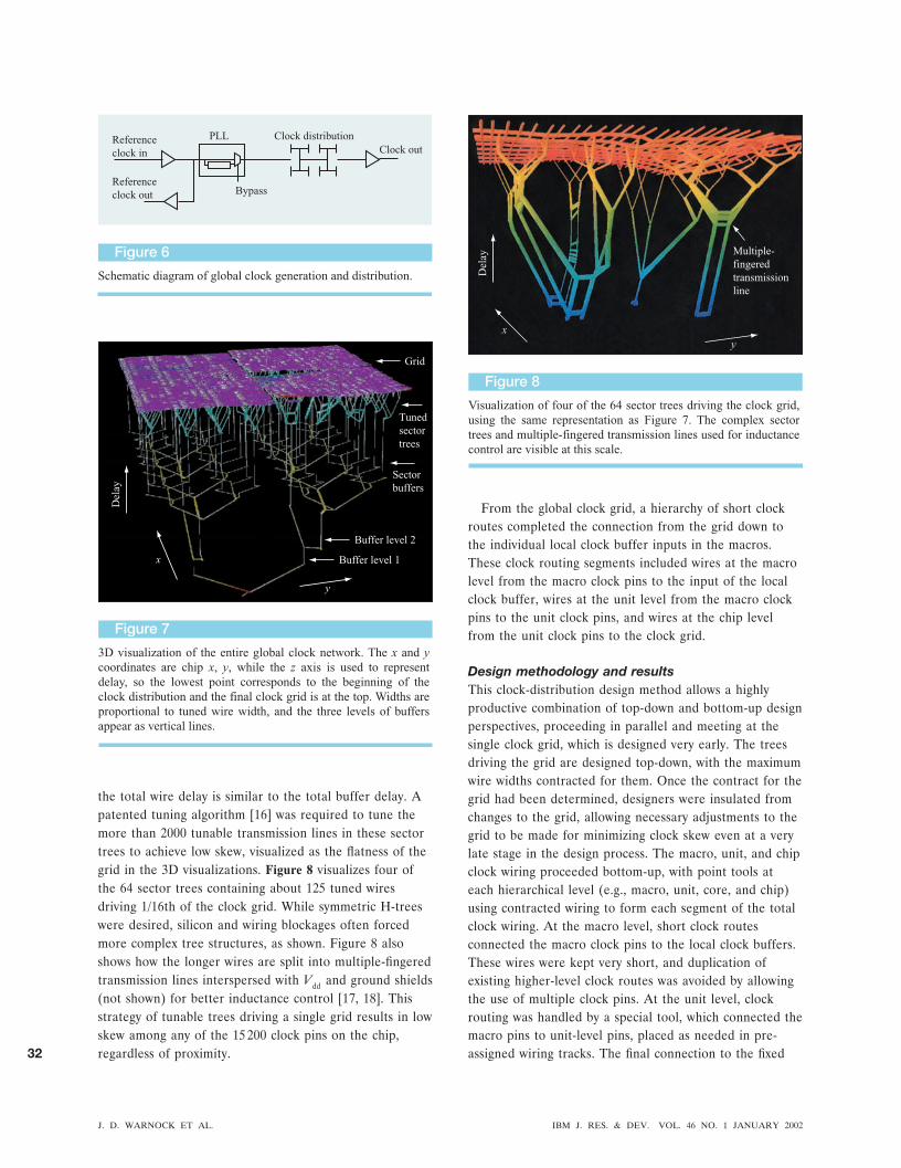
the total wire delay is similar to the total buffer delay. Apatented tuning algorithm [16] was required to tune themore than 2000 tunable transmission lines in these sectortrees to achieve low skew, visualized as the flatness of thegrid in the 3D visualizations. Figure 8 visualizes four ofthe 64 sector trees containing about 125 tuned wiresdriving 1/16th of the clock grid. While symmetric H-treeswere desired, silicon and wiring blockages often forcedmore complex tree structures, as shown. Figure 8 alsoshows how the longer wires are split into multiple-fingeredtransmission lines interspersed with Vdd and ground shields(not shown) for better inductance control [17, 18]. Thisstrategy of tunable trees driving a single grid results in lowskew among any of the 15 200 clock pins on the chip,regardless of proximity.
From the global clock grid, a hierarchy of short clockroutes completed the connection from the grid down tothe individual local clock buffer inputs in the macros.These clock routing segments included wires at the macrolevel from the macro clock pins to the input of the localclock buffer, wires at the unit level from the macro clockpins to the unit clock pins, and wires at the chip levelfrom the unit clock pins to the clock grid.
Design methodology and resultsThis clock-distribution design method allows a highlyproductive combination of top-down and bottom-up designperspectives, proceeding in parallel and meeting at thesingle clock grid, which is designed very early. The treesdriving the grid are designed top-down, with the maximumwire widths contracted for them. Once the contract for thegrid had been determined, designers were insulated fromchanges to the grid, allowing necessary adjustments to thegrid to be made for minimizing clock skew even at a verylate stage in the design process. The macro, unit, and chipclock wiring proceeded bottom-up, with point tools ateach hierarchical level (e.g., macro, unit, core, and chip)using contracted wiring to form each segment of the totalclock wiring. At the macro level, short clock routesconnected the macro clock pins to the local clock buffers.These wires were kept very short, and duplication ofexisting higher-level clock routes was avoided by allowingthe use of multiple clock pins. At the unit level, clockrouting was handled by a special tool, which connected themacro pins to unit-level pins, placed as needed in pre-assigned wiring tracks. The final connection to the fixed
Figure 6
Schematic diagram of global clock generation and distribution.
PLL
Bypass
Referenceclock in
Referenceclock out
Clock distributionClock out
Figure 7
3D visualization of the entire global clock network. The x and y coordinates are chip x, y, while the z axis is used to represent delay, so the lowest point corresponds to the beginning of the clock distribution and the final clock grid is at the top. Widths are proportional to tuned wire width, and the three levels of buffers appear as vertical lines.
Del
ay
Grid
Tunedsectortrees
Sectorbuffers
Buffer level 2
Buffer level 1
y
x
Figure 8
Visualization of four of the 64 sector trees driving the clock grid, using the same representation as Figure 7. The complex sector trees and multiple-fingered transmission lines used for inductance control are visible at this scale.
Del
ay Multiple-fingeredtransmissionline
yx
J. D. WARNOCK ET AL. IBM J. RES. & DEV. VOL. 46 NO. 1 JANUARY 2002
32

clock grid was completed with a tool run at the chip level,connecting unit-level pins to the grid. At this point, theclock tuning and the bottom-up clock routing process stillhave a great deal of flexibility to respond rapidly to evenlate changes. Repeated practice routing and tuning wereperformed by a small, focused global clock team as theclock pins and buffer placements evolved to guaranteefeasibility and speed the design process.
Measurements of jitter and skew can be carried outusing the I/Os on the chip. In addition, approximately 100top-metal probe pads were included for direct probingof the global clock grid and buffers. Results on actualPOWER4 microprocessor chips show long-distanceskews ranging from 20 ps to 40 ps (cf. Figure 9). This isimproved from early test-chip hardware, which showedas much as 70 ps skew from across-chip channel-lengthvariations [19]. Detailed waveforms at the input andoutput of each global clock buffer were also measuredand compared with simulation to verify the specializedmodeling used to design the clock grid. Good agreementwas found. Thus, we have achieved a “correct-by-design”clock-distribution methodology. It is based on our designexperience and measurements from a series of increasinglyfast, complex server microprocessors. This method resultsin a high-quality global clock without having to usefeedback or adjustment circuitry to control skews.
Circuit designThe cycle-time target for the processor was set early in theproject and played a fundamental role in defining thepipeline structure and shaping all aspects of the circuitdesign as implementation proceeded. Early on, criticaltiming paths through the processor were simulated indetail in order to verify the feasibility of the designpoint and to help structure the pipeline for maximumperformance. Based on this early work, the goal for therest of the circuit design was to match the performance setduring these early studies, with custom design techniquesfor most of the dataflow macros and logic synthesis formost of the control logic—an approach similar to thatused previously [20]. Special circuit-analysis and modelingtechniques were used throughout the design in order toallow full exploitation of all of the benefits of the IBMadvanced SOI technology.
The sheer size of the chip, its complexity, and thenumber of transistors placed some important constraintson the design which could not be ignored in the push tomeet the aggressive cycle-time target on schedule. Theseconstraints led to the adoption of a primarily static-circuitdesign strategy, with dynamic circuits used only sparinglyin SRAMs and other critical regions of the processor core.Power dissipation was a significant concern, and it was akey factor in the decision to adopt a predominantly static-circuit design approach. In addition, the SOI technology,
including uncertainties associated with the modelingof the floating-body effect [21–23] and its impact onnoise immunity [22, 24 –27] and overall chip decouplingcapacitance requirements [26], was another factor behindthe choice of a primarily static design style. Finally, thesize and logical complexity of the chip posed risks tomeeting the schedule; choosing a simple, robust circuitstyle helped to minimize overall risk to the projectschedule with most efficient use of CAD tool and designresources. The size and complexity of the chip alsorequired rigorous testability guidelines, requiring almostall cycle boundary latches to be LSSD-compatible formaximum dc and ac test coverage.
Another important circuit design constraint was thelimit placed on signal slew rates. A global slew rate limitequal to one third of the cycle time was set and enforcedfor all signals (local and global) across the whole chip.The goal was to ensure a robust design, minimizingthe effects of coupled noise on chip timing and alsominimizing the effects of wiring-process variability onoverall path delay. Nets with poor slew also were foundto be more sensitive to device process variations andmodeling uncertainties, even where long wires and RCdelays were not significant factors. The general philosophywas that chip cycle-time goals also had to include theslew-limit targets; it was understood from the beginningthat the real hardware would function at the desiredcycle time only if the slew-limit targets were also met.
The following sections describe how these designconstraints were met without sacrificing cycle time. Thelatch design is described first, including a description ofthe local clocking scheme and clock controls. Then thecircuit design styles are discussed, including a description
Figure 9
Global clock waveforms showing 20 ps of measured skew.
1.5
1.0
0.5
0.0
0 500 1000 1500 2000 2500
20 ps skew
Vol
ts (
V)
Time (ps)
IBM J. RES. & DEV. VOL. 46 NO. 1 JANUARY 2002 J. D. WARNOCK ET AL.
33

of some of the special techniques used to enhanceperformance. Finally, the implementation of both customdataflow designs and control RLMs is discussed.
Latch designBy far the majority of the latches in the design wereconventional transmission-gate master–slave flip-flops,as shown in Figure 10. These latches were designed to
minimize exposure to noise-induced upset, to provide alow soft-error-rate (SER) exposure, and to be generallytolerant of a certain amount of local clock skew. Ingeneral, designers were given some degrees of freedomin specifying the latch parameters, and the final designswere subject to a layout-based checking routine to verifycompliance with all latch, clocking, and other circuitdesign rules. As shown in Figure 10, designers wereallowed to customize the logic gate which drives into thefirst transmission gate, thereby minimizing the overheadimposed by the latch. The transmission gates and the twoinverters in the data path could also be sized by designers(within specified limits) in order to separately control andoptimize the latch power, setup time, and clock-to-data-out delay.
The two local clock phases (c1 and c2), as well as thescan clock, were derived locally from one tap of the globalclock, as shown in Figure 11. Each local clock buffercontained two control inputs for test and debug capability.In addition, where extra margin was needed for protectionagainst race conditions, the designer could make use ofthe “local_u” setting as shown, in order to delay the risingclock edge on a buffer-by-buffer basis. The “global_u”signals were sourced from scan-only latch banks insidethe functional units, and were used to selectively delaythe rising clock edge for debugging purposes. Each globalsignal was routed to a large number of local clock buffers,with a partitioning strategy determined by the circuit andlogic teams. The stop controls were pipelined from thechip onboard processor (COP) to all clock buffers acrossthe chip, with the final segment from the local pipelinelatch into the buffer having to occur in half a clock cycle.The c1 and scan clock buffers had separate stop controls,allowing arbitrary sequencing of the scan and c1 (system)clocks. For most of the latches, the c2 clock was free-running, with the stop signal tied to ground. However,outside the processor core, certain regions of logic weredesigned to operate at integer multiples of the core cycletime. In this case, pipeline stop signals were used to fireboth c1 and c2 clocks in a programmable fashion, therebysetting the frequency for logic operation in a givendomain. For example, firing the clocks on alternate cycleswould be appropriate for a 2:1 frequency reduction, everythird cycle for 3:1 operation, etc.
For critical timing paths, designers were given themeans to reduce the overhead imposed by the standardflip-flop, which included two embedded inverters and abuilt-in setup time penalty for potential clock skew,process variability, and across-chip linewidth variation(ACLV). Separate master and slave latch designs wereprovided, which could be inserted at arbitrary points inthe logic. As shown in Figure 12, this allows logic signalson critical timing paths to propagate through alternating
Figure 10
Standard transmission-gate master–slave flip-flop with LSSD capability. The input logic gate is specified independently by the designer, with constraints on gate type, drive strength, and physical proximity.
scan_in
scan_out
data_in data_out
c1_b
c1_bc1
c2_bc2
c1_b
c1
c1
c2
c2
c2_b
c2_bscanclk_b
scanclk_b
scanclk_b
scanclk
scanclk
scanclk
l1 l2Attachedlogicgate
Figure 11
Local clock buffers for master–slave latch, including pipeline latches for ac test control signals. The pin “local_u” can be tied either to a supply (“nominal” case) or to the global clock (rising edge delayed) on a buffer-by-buffer basis. Pipeline latches for COP control signals were usually shared among a number of local clock buffers.
c1_stop
c1
c2
c2_stop
global_clk
global_clk
c1_global_u_b
c2_global_u_b
c1_local_u
c2_local_u
scanclk_stop
global_clk
scanclk_global_u_b
scanclk_local_u
scanclk
COPlogic
COPlogic
J. D. WARNOCK ET AL. IBM J. RES. & DEV. VOL. 46 NO. 1 JANUARY 2002
34

cycle-boundary (master, or c1) and mid-cycle (slave, orc2) latches without incurring a setup time penalty. Latchplacement is also simplified. On average, a half cycle oflogic is allowed between c1 and c2 latches or betweenc2 and c1 latches. However, less logic between any twolatches means that time is given up to the logic followingthe receiving latch, and more logic means that time istaken from the following logic. Figure 13 shows anexample of a master-only latch with LSSD compatibility[2]. The area overhead for LSSD compatibility issignificant in this case, since an additional c2 latch mustbe provided (aside from the separate c2 added to thedownstream logic) for scan functionality. However, even inthis situation, the extra area was a relatively small additionto the overall total, and the flexibility of this schemewould often allow area savings in other parts of thedesign.
Although the split-latch scheme offered many benefitsin terms of its flexibility, resistance to clock skew, processvariation, and overall reduction of the latch overhead oncritical paths, there were some substantial drawbacks tothe use of these latches in the processor design. Mostnotable among these was the increased difficulty of timingpaths through logic containing these latches. The timingtool had to be able to deal with multi-cycle paths throughtransparent latches, including loops and other difficulttopological situations, and then had to present the timingdata in an intelligible way. In addition, there were certainac test issues which had to be addressed, including the factthat it became difficult to assess how many back-to-backcycles would be needed to capture all of the critical timingpaths through the machine. Also, ac timing failures couldbecome much more difficult to debug, at least in principle.
Circuit stylesFor reasons mentioned earlier, complementary staticcircuits were used predominantly in the design. Thedesigners were allowed to use these circuits with fewrestrictions. Limits were placed on effective beta ratio(p-to-n strength ratio), minimum device size (for trackingand process variability concerns), maximum stack height,and node slew (for noise, tracking, and process/modelsensitivity reasons). Although the maximum allowed stackheights were 4 and 3 for n-FETs and p-FETs, respectively,the recommended procedure was to limit designs(especially in timing-critical paths) to 3 and 2 forn-FETs and p-FETs, respectively. This recommendationwas made on the basis of the sensitivity of wide gates tosimultaneously switching inputs, model uncertainties in thelinear regime of the device operation, sensitivity to bodyvoltage, and the desire to avoid having any one gate oronly a few gates contribute a large fraction of the delayin a given cycle.
The technology also offered reduced-Vt (thresholdvoltage) n-FET and p-FET devices, which provided aperformance improvement of about 10% over the standardVt counterparts, but at the cost of higher off-state leakagecurrents. Therefore, it was desirable to use these low-Vt
devices selectively, in only the most timing-critical parts ofthe design. The process technology was planned such thatthe ground rules allowed swapping from normal Vt to lowVt at the last moment, usually with minimal or no other
Figure 12
Split-latch clocking diagram. c1 and c2 latches are transparent on alternate half-cycles, allowing logic to propagate through successive cycles of logic in a way that is tolerant of any local clock skew. In addition, variability in timing delays due to modeling uncertainty or process linewidth variation can be averaged out over several cycles, since time can be “borrowed” from the following cycle if the signal arrives a little late at a given latch, or “given” to the following cycle if the signal is early.
Clock
Transparent Transparent Transparent
c1 c1c2Logic A Logic B
Figure 13
Scannable split-latch (c1) design. Designers were allowed to tune the transmission gate size, and could specify input and output gates (with constraints on gate type, drive strength, output load, and physical proximity).
scan_in
data_in data_out
c1_b
c1_bc1
c2_bc2
c1_b
c1
c1
c2
c2
c2_bc2_b
scanclk_b
scanclk_b
scanclk_b
scanclkscanclk
scanclk
Attachedlogicgate
Attachedlogicgate
scan_out
Inputs from other latchesor logic gates
IBM J. RES. & DEV. VOL. 46 NO. 1 JANUARY 2002 J. D. WARNOCK ET AL.
35

effect to the circuit layout. In this way, the decision to uselow-Vt devices could be postponed until near the end ofthe design process, and low-Vt devices could be selectivelyemployed only where necessary. Overall, less than 10%of the logic transistors were implemented with low-Vt
devices, thereby avoiding a large increase in chip standbycurrent while still capturing the performance benefit ofthese devices.
One particular benefit of using static circuits in thedesign was that this design style allowed designers to makefull use of various design automation aids, including anadvanced circuit tuner [28, 29] providing rapid designturnaround for investigation of different circuit topologiesand implementations, and detailed performance tuningbased on layout parasitics. An example of how this processworks is shown in Figure 14 [30]. In the instruction-fetch/branch unit, these techniques were used to build aseries of eight compact static carry-lookahead Ling adders[31] used for branch-target address calculation. The delaythrough the 24-bit adder and built-in four-way multiplexorwas reduced to about 400 ps (or a little over 9 FO4, whereone FO4 delay unit is the average delay of an inverterwith a fan-out of 4). This adder ended up being nearly asfast as the dynamic adder originally considered for thisfunction, but at a fraction of the cost in terms of power,and with improved allowance for overhead routability.
In addition to complementary static circuits, an attemptwas made to use certain circuit styles thought to be moreoptimal for use in SOI technology. One such family usedwas complementary passgate logic (CPL), an example ofwhich is shown in Figure 15. In these circuits, couplingbetween source/drain and the body of the passgate devicehelps to raise the body voltage during a 0 3 1 transition,lowering the threshold voltage and speeding the transition.However, such circuits tend to operate in regions wherethe device models are less accurate, they are sensitive tovariations in threshold voltage (especially in the linearregime), and they are also typically very sensitive tohistory-dependent delay effects [32]. These issues meantthat substantial extra design timing margin had to beadded to ensure that these circuits met the chip cycle-time design targets.
Another circuit style used rather widely involvednetworks of transmission-gate circuits, an example ofwhich is shown in Figure 16 [error check and correction(ECC) logic in the L2 control]. Since the ECC function ison the critical path for accessing the L2 cache upon an L1miss, the Hamming matrix was optimized for the lowestnumber of logic levels and highest number of shared termswithout compromising the single-error correction– double-error detection (SEC–DED) requirement. The X(N)OR4gate was the best choice as a compact fast building blockfor this function, since the H-matrix could be optimizedto map directly into such a gate representation with aminimum number of terms. XOR logic functions areparticularly well suited for implementation with passgatenetworks, and the addition of the complementary p-FETin each transmission gate, along with careful gate tuningand slew optimization, ensured that the design had therequired degree of robustness and insensitivity to processvariations. The use of low-Vt gates was also very effective
Figure 14
Rapid-turnaround-time semicustom design process. Design auto-mation at each step allowed rapid iteration and optimization of the design, and also provided a means of exploring a much wider design space than would otherwise have been possible.
Schematic, builtwith set of
two-parametergates
Autogeneratecompatible
layoutsfor all gates
Tune withtuner
Timing,checking,
verification
Parasiticextraction
Layout
Place androute
Parasiticcap info
Userconstraints
Res
truc
ture
, if
nece
ssar
y
Figure 15
Circuit schematic of part of the 3:2 compressor used in the floating-point multiplier array, implemented in CPL logic.
sum_b sum
a_xnor_ba_xor_b
a_ba
b_b
b
c_b
c
J. D. WARNOCK ET AL. IBM J. RES. & DEV. VOL. 46 NO. 1 JANUARY 2002
36

in improving the speed and slew characteristics of thesecircuits.
Finally, a number of dynamic circuits were used on thechip for certain critical applications. The usage of dynamiccircuits was limited to some of the register files, arraycircuitry, and some circuitry in the load/store unit,designed to interface smoothly with the dynamic circuitryin the data cache array. Both footed and non-footeddomino circuits were used, with special techniques used toovercome unique SOI noise issues [24, 25] and a variety oftools to check for noise exposures or other weaknesses inthe design. In addition, any half-cycle timing paths weredesigned with extra margin to account for possible duty-cycle variations in the clock waveforms.
Circuit design and layoutThe most critical designs employed full-custom techniquesfor both the circuit design and the subsequent layout.Critical design aspects which drove this level ofcustomization could include timing/cycle-time issues, areaissues, and/or routability/wiring issues. These designs(usually dataflow structures), typically took the longestamount of time to implement, but offered the mostperformance potential, with generally more optimal usageof area and wire resources. Often these designs containedmany reusable components (multiplexors, latch cells, clockbuffers, etc.) in order to reduce the resources required forimplementation. In addition, larger blocks inside custommacros (adders, incrementors, comparators) were oftenbuilt using the semicustom techniques described in theprevious section. Area, power, pin placement, and timingof these macro sub-blocks could be customized dependingon the application. A typical custom macro partition mightcontain from 20 000 to 50 000 transistors. Overall, the chipcontained more than 400 unique custom macro blocks.
“Bit stacking” of standard-cell library “books” wasanother technique used successfully for implementationof certain large dataflow structures in regions of the chipwhere area and wiring channels were at a premium.As the name suggests, large structures were organizedin a dataflow-like manner, with special techniques used toorganize and place the individual library books. Thisallowed fast implementation of complex dataflowstructures, with considerable ability to make changes latein the design cycle, while still maintaining the dataflowstructure to minimize usage of wiring resources and toorganize the flow of signals/data through the logic.
Control logic and standard-cell libraryThe control logic was implemented in the form ofdiscrete RLMs, implemented with gates from astandard-cell library [33]. The control logic wassynthesized from the high-level VHDL description, withvarious degrees of customization and optimization options
available to improve the initial result from synthesis.After synthesis, a variety of specialized place-and-routetechniques were used to implement the design, withiterations back through an incremental synthesis processto optimize the clock network, tune critical timing pathsthrough the design, and fix node slew violations. In somecases, the resulting design was extracted and timed usingthe same methodology as that used for the custom macros,although in many cases the RLM was timed at the gatelevel, using the library timing rules. In either case, thisautomated design flow allowed control logic debug andtiming work to continue to a very late stage in the designprocess without gating the schedule of the final design tape-out. This allowed the control logic to be implemented insuch a way that it did not limit the overall chip cycle time.
The structure and the various special features of thestandard-cell library were crucial to the success of theeffort to close timing on the control logic. The libraryconsisted of a relatively narrow series of simple logicgates, but each logic gate was supported with a widematrix of options including a broad range of devicewidths, tapered stacks, several n:p width ratios, andnormal- vs. low-device-threshold-voltage (Vt) books(Table 3). The goal was to allow the designer to achievea result which was as close to a full-custom result aspossible. To this end, a number of special latch cellswere built with an integrated logic book (Figure 17),which allowed merging logic with the latch cell butavoided exposure of the latch transmission gate inputto potentially noisy wires. Split-latch designs were also
Figure 16
An xor4 gate used in the error check and correction (ECC) logic in the L2 control, implemented with low-VT gates. The ECC logic function was well suited to implementation with transmission gate circuits.
in0
in1
in2
in3xnor23
xnor01
xor01
out
xor23
IBM J. RES. & DEV. VOL. 46 NO. 1 JANUARY 2002 J. D. WARNOCK ET AL.
37

available, with an integrated front-and-back logic gate(Figure 18). These designs gave the RLM designeralmost the same ability as the custom designer to minimizethe latch overhead and provide for clock-skew-tolerantoperation.
The library also supported a number of optimizationprocedures which could be carried out after all otherphysical design steps were completed, without requiring
any placement or wiring changes. On critical paths, thefinal, layout-based macro timing could be improved byautomatically replacing standard-Vt books with their low-Vt counterparts, which were designed to have completelycompatible footprints. This technique ensured that suchlow-Vt books (with higher performance but also higherleakage) were used only where necessary. In addition, alllatch books which were not driving critical signals could be
Figure 17
Library master–slave flip-flop with integrated front-end logic gate choices.
scan_in
data_in I2I1
c1_b
c1_bc1
c2_bc2
c1_b
c1
c2_b
c2
c1 c2
c2_bscanclk_b
scanclk_b
scanclk_b
scanclk
scanclk
scanclk
scan_out
Input gate:eight choices
Latch body:two choices• low power• normal power
Output buffer:two choices• light load• heavy load
Table 3 Standard-cell library composition (excluding latches and clock buffers), showing the width and depth and some of thespecial features available. Limited numbers of special-purpose cells, including XOR/XNOR gates, were also included in the library.
Logic gate Beta ratiosavailable
Power levels(input cap)
Number ofVt options
Number oftapered cells
Total numberof cells
INV 5 34 2 0 340
NAND2 5 29 2 28 318NAND3 4 23 2 22 206NAND4 3 16 2 0 96
NOR2 5 16 2 16 176NOR3 3 6 2 0 36
AOI21 5 16 2 0 160AOI12 5 16 2 0 160AOI22 5 16 2 0 160
OAI21 5 16 2 0 160OAI12 5 16 2 0 160OAI22 5 16 2 0 160
J. D. WARNOCK ET AL. IBM J. RES. & DEV. VOL. 46 NO. 1 JANUARY 2002
38

replaced with low-power books (along with the local clockbuffer), again with footprint-compatible cells. Since a largefraction of the chip power was devoted to clocking andlatching, this technique was able to offer significant powersavings in the RLM macros. Finally, all white spaceinside the RLMs was filled with a combination of specialdecoupling capacitor cells and a gate-array backfill. Thegate-array backfill could be customized into logic gates(inv, nand2, nand3, nor2) using only the metal designlayers, allowing logic fixes to be made with changes toonly the metal layers. This quick-fix capability allowed forfaster turnaround of late logic fixes, significantly speedingup the overall system bringup time.
Power distributionThe design of the power-distribution network had threeprincipal constraints based on our previous experience.First, the average dc voltage drop for the chip had tobe limited to less than 30 mV for power densities up to1 W/mm2. Second, transient power fluctuations occur whenthe total chip power changes abruptly over a few cycles,causing the power supply to oscillate at the resonantfrequency of the package/chip; the power network designhad to limit such fluctuations to be less than �10% of the
nominal power supply. And finally, the common-modenoise on global interconnects had to be less than 200 mVfor the worst-case wide-bus activity.
Because similar objectives had been imposed on earlierIBM microprocessor designs, the methods for analyzingand accomplishing the first two targets were wellunderstood: A dc circuit analysis of the proposed powergrid in regions with sparse power and ground C4s wouldpredict worst-case dc drop with sufficient accuracy. Aseries of transient analyses of the chip/package duringmaximum power change would predict how muchdecoupling capacitance was required to hold fluctuationsto 10% of supply voltage. For a total POWER4 chippower of �115 W and a maximum transient powerchange of �25 W, it was necessary to embed 250 nFof decoupling capacitance into critical areas of the chip.
These values of the total chip power and the maximumtransient power change were determined by combiningcircuit power analysis results with unit-level logicsimulation results. The circuit power analysis yieldedpower-dissipation equations as functions of input switchingfactors, while the logic simulation analysis yielded worst-case switching factors on a unit-by-unit basis.
The circuit power equations were obtained by analyzingevery circuit and macro schematic with CPAM [34].
Figure 18
Split-latch design for standard cell library, showing front- and back-end logic gate choices. For the output gate, the latch drives one input; other inputs come from other logic blocks (same clock phase as latch output).
scan_in
data_in data_out
c1_b
c1_bc1
c2_bc2
c1_b
c1
c1
c2_bc2_b
c2
c2
scanclk_b
scanclk_b
scanclk_b
scanclkscanclk
scanclk
scan_out
Input gate:eight choices
Latch body:one choice
Output gate type:six choices �two load choices
IBM J. RES. & DEV. VOL. 46 NO. 1 JANUARY 2002 J. D. WARNOCK ET AL.
39
CPAM is an IBM power-analysis tool that uses IBMACES1 as its simulation engine, enabling it to analyzecircuits of up to 500 000 transistors. CPAM also takes intoaccount logic orthogonality between inputs. With test andcontrol inputs set at functional states, CPAM is first runto determine the power with only the clocks toggling andthen rerun to determine the power with “random” inputvectors applied to the circuit. During the second poweranalysis, CPAM controls the switching factor betweenconsecutive input vectors to a user-specified value—typically 50%.
The worst-case switching factors were obtained byhaving the chip architects define worst-case simulationpatterns. These patterns were run on both the core andfull-chip logic models using the IBM TEXSIM logicsimulator. Switching factors were obtained by simplycounting the number of times each node toggled ona unit-by-unit basis and dividing by the number ofsimulation cycles.
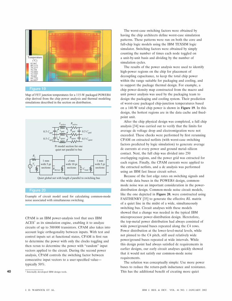
The results of the power analysis were used to identifyhigh-power regions on the chip for placement ofdecoupling capacitance, to keep the total chip powerwithin the range suitable for packaging and cooling, andto support the package thermal design. For example, achip power-density map constructed from the macro andunit power analysis was used by the packaging team todesign the packaging and cooling system. Their predictionof worst-case packaged chip-junction temperatures basedon a 140-W total chip power is shown in Figure 19. In thisdesign, the hottest regions are in the data cache and fixed-point unit.
After the chip physical design was completed, a full chipanalysis [34] was carried out to verify that the limits foraverage dc voltage drop and electromigration were notexceeded. These checks were performed by first rerunningCPAM on extracted netlists (with worst-case switchingfactors predicted by logic simulation) to generate averagedc currents at every power and ground metal–siliconcontact. Next, the full chip was divided into 250overlapping regions, and the power grid was extracted foreach region. Finally, the CPAM currents were applied tothe extracted netlists, and a dc analysis was performedusing an IBM fast linear circuit solver.
Because of the fast edge rates on switching signals andthe wide data buses in the POWER4 design, common-mode noise was an important consideration in the power-distribution design. Common-mode noise circuit models,like the one depicted in Figure 20, were constructed usingFASTHENRY [35] to generate the effective RL matrixof a quiet line in the midst of a wide, simultaneouslyswitching bus. Circuit analyses with these modelsshowed that a change was needed in the typical IBMmicroprocessor power-distribution design. Heretofore,the top-metal power distribution had always consisted ofwide power/ground buses repeated along the C4 rows.Power distribution at the lower-level-metal levels, whilenot pinned to the C4 pitch, still used relatively widepower/ground buses repeated at wide intervals. Whilethis design point had always satisfied dc requirements inearlier designs, our early circuit analyses quickly showedthat it would not satisfy our common-mode noiserequirements.
The solution was conceptually simple: Use more powerbuses to reduce the return-path inductance and resistance.This has the additional benefit of creating more quiet1 Internally developed IBM design tools.
82.00780.117378.227776.33874.448372.558770.66968.779366.8897
Temperature(�C)
Figure 19
Map of FET junction temperatures for a 115-W packaged POWER4 chip derived from the chip power analysis and thermal modeling simulations described in the section on distribution.
Figure 20
Example of circuit model used for calculating common-mode noise associated with simultaneous switching.
Pi model section for onequiet net parallel to bus
0.5 Cgnd
0.5 Cquiet
0.5 Cgnd
0.5 Cquiet
Lactive Ractive
Rs
Rdevice Cload
Vs
Lgnd Rgnd
Lquiet Rquiet
1 mmwith 5 pisections
1 mmwith 5 pisections
d mmwith 10 pisections
Quiet global net with length d parallel to switching bus
J. D. WARNOCK ET AL. IBM J. RES. & DEV. VOL. 46 NO. 1 JANUARY 2002
40

wiring tracks, but required additional (scarce) wiringtracks. Some additional tracks were obtained byredesigning and qualifying a new rectangular metal C4 paddesign, and, after considerable analysis and negotiationwith unit and chip integrators, the power grid that cameclosest to meeting the dc-noise, common-mode-noise,quiet-wiring-track, and wirability requirements was afourteen-wiring-track image. This is depicted in Figure 21along with predictions for worst-case common-mode noise.It devotes four wiring tracks to power and ground and tenwiring tracks to signal wiring. Because portions of thedesign were unable to strictly conform to this image,exceptions were allowed provided that some roughguidelines were followed: Power and ground should useat least 25% of the wiring tracks, and no more than tensignal wires were permitted between power buses.
IntegrationThe integration cycle begins with floorplanning at therespective level of hierarchy: unit, core, or chip. Thenetlist is built from the VHDL description through acompilation process utilizing both high-level (Hiasynth)and low-level (BooleDozer) synthesis. The resulting netlistis then imported into the Cadence design framework inthe form of an autoLayout view. The design frameworkserves as the repository of the design data for all designelements: custom, RLM, unit, core, chip. The newautoLayout view is initialized with any previousfloorplanning information.
FloorplanningOnce the floorplan is created, the integrator sets the blocksizes and aspect ratios through a set of iterative moves.The floorplanning environment allows for rectilinearshapes on blocks to maximize area utilization. Size andaspect ratios are communicated to each block ownerfor feedback. Once block sizes and aspect ratios areestablished, pin assignment and track allocations aremade.
Significant over-block routing is utilized to minimizewire length, reduce congestion, and improve timing. Tofacilitate over-block routing, detailed blockage contractsare established between adjoining upper (parent) andlower (child) members of the hierarchy. These contractsspecify the exact routing tracks on each routing layerwhich are used by the parent and child. The childblockage is represented to the parent in the form of anabstract. Every floorplannable object has an abstract:custom, rlm, unit, core. The child uses an inverse imageof the abstract (a cover) to perform internal routing. Thecover is automatically derived from the abstract. If a childshell needs to share chip-level resources, an additionalcover (the parent_cover) is needed which is a union of allof the chip infrastructure that appears above all instances
of the child. This view is automatically generated at eachlevel of hierarchy and propagated downward to the leafcells. Additional constraints are also enforced in theabstract/cover to ensure smooth child/child andparent/child interaction. For example, the parent “owns”the routing track immediately outside the outline of thechild for purposes of adjacent via rules. Therefore, thechild’s cover contains additional via blockages to preventvia placement on the track immediately inside the outlineof the child. Once a blockage contract is established, pinassignment can be performed on the child cells. Pins areassigned only on routing tracks owned by the child. In thisway, accessibility from within the child is guaranteed, andthrough-tracks assigned to the parent are not interruptedby child pins. Pins are predominately assigned at theperimeter of blocks. However, pin placement anywherewithin the child outline is allowed. Pins must be accessibleto the parent from the pin layer or any layer above thepin. Pins must be accessible to the child from the pin layeror any layer below. Via obstructions are placed above orbelow the pins in the respective cover or abstract toensure that the parent and child do not conflict ata pin.
Figure 21
Example of common-mode noise simulation results. Noise on quiet wires is calculated for several different switching assump-tions on nearby wires. Inset shows a cross section of the 14-bit image with power wires shaded.
Quiet M3 with 100%M7/M5 activity
Quiet M4 with 100%M6 activity
Quiet M4 with 100%M6 activity
Quiet M3 with 100%M7/M5 activity
Quiet net length (mm)
Rising waveformapproaching quiet sink
Rising waveformapproaching quiet source
Bitimage
0.20
0.10
0.00
�0.10
�0.20
�0.300.0 0.5 1.0 1.5 2.0 2.5 3.0 3.5 4.0 4.5 5.0
Qui
et n
et n
oise
(V
)
M7
M6M5M4M3M2
IBM J. RES. & DEV. VOL. 46 NO. 1 JANUARY 2002 J. D. WARNOCK ET AL.
41

Architecturally significant buses received specialattention during the floorplanning of units, core, and chip.Net length guidelines were established during floorplanningto control time-of-flight and slew rates of nets. The largesize of most units meant that buses could not span theunit without intermediate buffers or latches. Therefore,the locations of buses, buffers, and latches were plannedearly in the process so that changes could be incorporatedinto the architecture. In addition, in areas where busesspanned large distances over a unit, buffer locations wereestablished, and “holes” were opened in the unit toaccommodate the buffer. The buffer or latch blockageand power pins are reflected in the parent_cover of the child.Nets which were not timing-sensitive or architecturallyimportant were routed around large units, where theycould be buffered and latched at appropriate intervals.
RLM buildThe random logic macro (RLM) build methodology wasdesigned as a complementary process to create high-performance synthesized control blocks for each level ofthe floorplan. The process that was defined uses iterativetiming-driven design at all levels: synthesis, placement,clock insertion and optimization, routing, and post-placement/routing optimization. The flow uses a combinationof internal synthesis tools and transformations, qplace fortiming-driven placement, and wroute for timing-drivenrouting.
The RLM build process begins with synthesis of a netlistfrom VHDL using wire-load models derived from actualphysical parameters of numerous completed RLMs. In thisinitial netlist, the clock network is not fully implemented.A local clock buffer (LCB) for each unique clock-phasecombination is connected to all of the correspondinglatches. In addition, a single clock control block (LCBdriver) is connected to all LCBs. Next, an initial timing-driven placement is performed while ignoring the clock,scan, and miscellaneous control nets and with the LCB andLCB driver blocks placed at the origin. The placement givesthe optimal data-path placement in order to achievetiming without consideration of the clock network. Clocknetwork insertion is performed on the basis of thisplacement. During this phase, the correct number of LCBsare inserted and connected to the correct number oflatches to meet clock-distribution constraints. An initialLCB placement is made, and all of the associated latchesare placed in a placement region around the LCB. A secondtiming-driven placement is then performed, with the LCBlocations fixed and the latches allowed to float within theirrespective regions. Next, routing is performed in twosteps. First, the clock network from RLM input pins to theinput pins of the LCBs receives a network of virtual pinsand subnets to replace the original net. This allows forstraight point–point routing from the input pins to the LCB.
During this phase, the clock nets from the LCBs to thelatches are also weighted to provide priority routing.Timing-driven routing is performed on the entire RLM, withthe clock nets receiving priority over signal nets. At theconclusion of the route, the design can be modified withpost-physical design synthesis transforms to optimizeperformance. The design can then be incrementally placedand routed to correct any changes.
Infrastructure and wiringThe chip infrastructure comprises all of the necessarydesign elements to distribute clock, power, and I/O toobjects in the floorplan. These three portions of thedesign use the topmost levels of thick, wide metal tocontrol RC delay, IR drop, and impedance. Since thesethree portions consume a large amount of wiring resourceand in many cases compete for the same routing areas,they must be designed and optimized concurrently.
The infrastructure design process begins with signal I/Oassignment based on the floorplan positions of criticalcomponents. Feedback is also incorporated from thepackage to modify the location of signal I/O. Next, aninitial clock distribution is created with ideal bufferlocations. The I/O trunk wires and an initial powerdistribution are created using the top thick metal levels LMand MQ. A process of iteration is used to create the finalallocations for the signal I/O wires, clock distribution, andpower. Once this iteration process is complete, the finaldetermination of the location, widths, spaces, and pitchesof the clock distribution, signal I/O trunks, and powerdistribution is complete. The remaining tracks on LM/MQare now available for the engineered buses.
Engineered buses are buses which are defined to bearchitecturally critical in maintaining performance.They typically control topological problems caused bythe need to span large floorplanned blocks. To improvethe performance of these buses, they are routed on thethicker, lower-resistance LM/MQ wiring levels. They may,in addition, be specified to be wider than the nominalLM/MQ wire width. Wire codes are used to model thesewires accurately in the chip timing environment. The listof engineered wires and the associated widths/spaces arederived from the wire codes to ensure that the engineeredroutes match the topologies estimated in timing.
To manage data volume and performance, a blockagemap and pin model are abstracted from the autoLayoutview of the design. At this point in the process, for netsthat require extremely exact placement to control delay,slew rate, or coupled noise, trunk routes are placed withSKILL code. The trunk routes can be point-to-point,contain one turn, or contain one “T” junction. ICCraftsman** is now used to complete the routes fromthe trunks to associated pins, and to route all otherengineered routes. IC Craftsman allows fully off-grid
J. D. WARNOCK ET AL. IBM J. RES. & DEV. VOL. 46 NO. 1 JANUARY 2002
42

routing of the engineered routes with extremely complexrules governing width, space, and neighboring nets. Thiscreates the most efficient use of routing resources for bothengineered and non-engineered routes. The engineeredroutes in POWER4 are shown in Figure 22; there areapproximately 35 000 such routes out of a total of 120 000nets at the chip level.
To complete the chip routing, a layout view of theengineered routes is abstracted and added to the chipautoPlaced view. Normal “non-engineered” routes arerequired to route around the blockages defined by theengineered routes. Non-engineered routes are routed on-grid. They can take the form of wide or normal-widthwires. Because of the on-grid routing, wide wires areinherently less efficient in the use of routing resources.Wide wires are routed first, by default, by wroute. Otherdefault-width wires are also priority-routed in groupsbased on criticality with the use of “selectNet” lists.Finally, all remaining noncritical nets are routed. Theentire process of routing normal routes takes approximately1.5 hours. This turnaround time was critical to ensure thatrapid timing learning could be achieved with extractedrouting information.
Global buffering of non-engineered nets is essentialto control propagation delay, slew-rate degradation,and coupled noise on long nets. Buffering rules wereestablished to screen nets that required buffering withoutthe need to do a timing run. For example, a single-cyclenet exceeding 3000 tracks in length required a buffer.Similar rules exist for multi-cycle and test nets. Tofacilitate rapid buffer insertion and timing, a set of toolswere developed to work with buffers that were pre-placedat each level of the hierarchy. For example, the chiphas approximately 450 32-bit buffer packs inserted asuniformly as possible throughout the floorplan. Initially,these buffer packs are inserted with all inputs groundedand the outputs floating. Two modes were used toaccomplish most of the needed buffering. In the first, theexact topology of the buffered net was described in a file.The files would then be interpreted and the net bufferedaccordingly. In the second, a net could be bufferedautomatically by finding the shortest path from the sourceto all sinks by traversing available buffer packs. Since theglobal buffering solution is not defined in the VHDL,it is necessary to reapply the solution each time a chip isinitialized with a new VHDL release. To facilitate this, acompanion tool wrote the existing buffering topology toa file, such that it could be reapplied on subsequentreleases.
Because of the number of nets at the chip level,rapid iteration to improve timing was necessary. Themethodology was established to complete a timingiteration daily. This included a review of the previoustiming run, buffer changes, a full chip global and final
route, 3D extraction of the routed data, and a full chip-timing run.
Checking strategyThe checking strategy was instrumental in ensuring thatthe final chip could be assembled with a minimum ofproblems. Because of the size of the chip, a large numberof problems at the end of the design cycle would be toodifficult to detect and fix. Therefore, the checkingmethodology was developed to treat each unit andthe core as a “chiplet.” In addition, a robust set of“methodology” checks were developed to ensure that allmacros, units, and the core could be correctly integratedat the next level of hierarchy.
In order to check an entity as a chiplet, it is necessaryto understand the environment in which the chiplet residesin the chip. To model this environment, the cover (routingcontract with the parent) and the parent_cover (fixed chip-level infrastructure) were added to the unit for DRC andLVS verification. Since the covers contain blockage layers,as opposed to manufacturable shapes, a separate set ofchecks were included for spacing of manufacturableshapes to blockages of the same layer. No minimum-areachecks were done on the blockage shapes, since they arenot required to comply with area rules. Similarly, theblockage shapes were considered during the LVS run forpurposes of determining shorts, since any manufacturableshape touching a blockage in a cover would be a short toa parent object.
Figure 22
Engineered buses in POWER4. The green (vertical) routes are in the MQ (sixth) wiring level; the lavender (horizontal) ones are in the LM (seventh).
IBM J. RES. & DEV. VOL. 46 NO. 1 JANUARY 2002 J. D. WARNOCK ET AL.
43

A separate-methodology DRC deck was created tocheck additional design constraints above and beyond thedesign rules necessary for manufacturing specified in theDRC deck. These checks concentrated on ensuringthe quality of the blocks as well as their ability to beintegrated at the next level of hierarchy. The types ofdesign constraints checked included ensuring that allmanufacturable shapes are “one-half ground rule” (i.e.,conform to a symmetric half of the shape definition, or“ground rule”) for the boundary of the floorplan block,power buses are on the correct periodicity, and clock pinsare in the correct track. Additional checks maintained thequality of the design for routing. For example, pins werechecked to ensure that they were on grid and accessiblefrom the same layer or the layer above.
Chip timing and extractionTiming closure at frequencies above 1 GHz in large,complex system-on-a-chip designs requires both thecapability for rapid iterative refinement and a high degreeof concurrency among timing activities occurring at alllevels of the design, including macro, unit, processor core,and chip. The scale and complexity of these timing tasksposed a major challenge to the POWER4 chip timingteam. In addition, the transparent latches described earlieradded to the difficulty of the timing task, with criticaltiming paths at the chip level frequently involving asmany as 10 to 20 stages of transparent latches traversingmultiple units. Finally, the timing methodology had to dealsimultaneously with multiple frequency domains, in whichcertain parts of the chip operated at different multiples ofthe global clock frequency. Since the exact multiple of theclock frequency used in these regions was programmable,the timing analysis had to provide the worst-case timingfor any selection of the multiple clock frequencies, forpaths potentially traversing more than one frequencydomain.
Hierarchical timing strategyTiming closure was pursued concurrently by the circuitand logic designers at the macro level, by the unit team atthe unit level, and by the global timing and integrationteam at the levels of the processor core, the memorysubsystem (GPS), and the chip (cf. Figure 2). The timingmethodology exploited the physical design hierarchy tofacilitate a “divide and conquer” approach to timingclosure. Because of the lack of hard timing boundariesat all levels of the hierarchy, this required frequentcommunication of updated timing contracts to reflecthow design changes in one block affected the timingrequirements of the other blocks in the design. This inturn drove the requirement for frequent timing iterationsat the chip level. Timing contracts were determinedhierarchically starting at the global chip level and then
propagated down the hierarchy through the processor coreand memory subsystem to the units and then on to theindividual macros. These contracts were generated nightlyfrom each chip-level timing run and consisted of input pinarrival times and slews, and output pin required times andlumped capacitive loads. Input arrival and output requiredtimes were both computed to distribute positive andnegative slack so as to provide individual macros andunits with contracts that, if achieved, would close timingglobally. Capacitive loads were computed as Ceff (effectivecapacitance seen at the driver output) as opposed to Ctot
(total lumped capacitance on the net) to model the effectof resistive shielding on long unit and global chip nets,and to optimize timing closure for minimum delay onwire-dominated paths. On the basis of these contracts,macro, unit, processor core, GPS, and chip timing allproceeded in parallel, passing information back and forthregularly to validate the ongoing work at all levels astiming was iterated toward global closure.
An important requirement of the hierarchical timingmethodology was the ability to incorporate a mixof (sometimes inconsistent) data with differingaccuracy/quality characteristics from different levels of thedesign hierarchy and from different regions of the design.This feature was essential, since different parts of thedesign proceeded toward completion at different rates.Early on in the design, chip-level timing was based on aninitial chip floorplan, using time-of-flight delays for unit-to-unit routes estimated in ChipBench*, the floorplanningtool which was also the interface to the IBM static timingtool, EinsTimer. Closure of timing at this level was usedto refine the floorplan and generate the first unit-timingcontracts. Unit-level timing was based on estimated delaysfrom the initial unit floorplans, with macro-level delaysfrom hand-coded Delay Calculator Language (DCL) rules,or with lists of asserted times required for macro inputs,and times at which macro outputs were available. As thedesign proceeded, these simple macro timing rules werereplaced by synthesized networks of standard-cell librarybooks (for RLMs), and timing rules (DCMs) for custommacros, based either upon macro schematic descriptionsor upon physical data extracted from layout. Estimatedwires at different levels of the hierarchy were graduallyreplaced with extracted data from real routed wires, untilfinally the whole chip was timed with data extracted fromthe physical design. At intermediate stages in the design,it was therefore necessary to use a mix of estimatedand/or incomplete data along with all the latest extracteddata as shown in Figure 23. A normal mix of design datacould include, for example, extracted SPICE2 RC networksfrom actual global routes at the chip level, in combination
2 SPICE: Software Process Improvement and Capability Emulation, an ISOstandard simulation process.
J. D. WARNOCK ET AL. IBM J. RES. & DEV. VOL. 46 NO. 1 JANUARY 2002
44
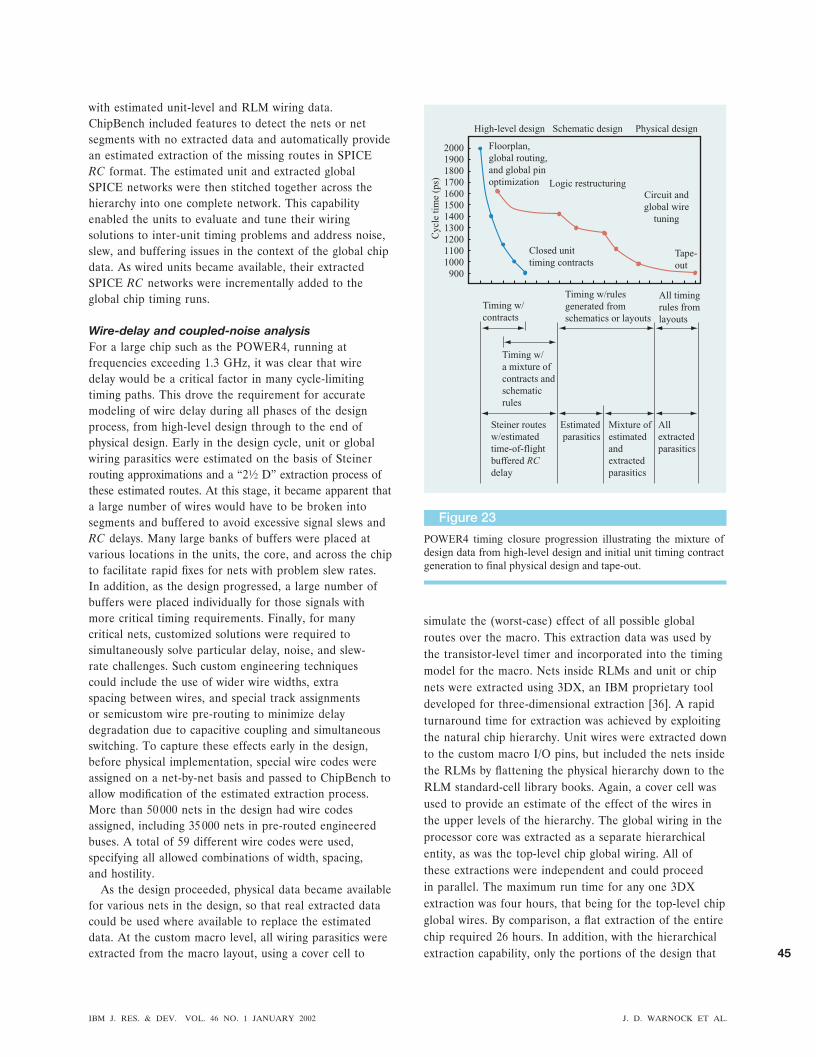
with estimated unit-level and RLM wiring data.ChipBench included features to detect the nets or netsegments with no extracted data and automatically providean estimated extraction of the missing routes in SPICERC format. The estimated unit and extracted globalSPICE networks were then stitched together across thehierarchy into one complete network. This capabilityenabled the units to evaluate and tune their wiringsolutions to inter-unit timing problems and address noise,slew, and buffering issues in the context of the global chipdata. As wired units became available, their extractedSPICE RC networks were incrementally added to theglobal chip timing runs.
Wire-delay and coupled-noise analysisFor a large chip such as the POWER4, running atfrequencies exceeding 1.3 GHz, it was clear that wiredelay would be a critical factor in many cycle-limitingtiming paths. This drove the requirement for accuratemodeling of wire delay during all phases of the designprocess, from high-level design through to the end ofphysical design. Early in the design cycle, unit or globalwiring parasitics were estimated on the basis of Steinerrouting approximations and a “21⁄2 D” extraction process ofthese estimated routes. At this stage, it became apparent thata large number of wires would have to be broken intosegments and buffered to avoid excessive signal slews andRC delays. Many large banks of buffers were placed atvarious locations in the units, the core, and across the chipto facilitate rapid fixes for nets with problem slew rates.In addition, as the design progressed, a large number ofbuffers were placed individually for those signals withmore critical timing requirements. Finally, for manycritical nets, customized solutions were required tosimultaneously solve particular delay, noise, and slew-rate challenges. Such custom engineering techniquescould include the use of wider wire widths, extraspacing between wires, and special track assignmentsor semicustom wire pre-routing to minimize delaydegradation due to capacitive coupling and simultaneousswitching. To capture these effects early in the design,before physical implementation, special wire codes wereassigned on a net-by-net basis and passed to ChipBench toallow modification of the estimated extraction process.More than 50 000 nets in the design had wire codesassigned, including 35 000 nets in pre-routed engineeredbuses. A total of 59 different wire codes were used,specifying all allowed combinations of width, spacing,and hostility.
As the design proceeded, physical data became availablefor various nets in the design, so that real extracted datacould be used where available to replace the estimateddata. At the custom macro level, all wiring parasitics wereextracted from the macro layout, using a cover cell to
simulate the (worst-case) effect of all possible globalroutes over the macro. This extraction data was used bythe transistor-level timer and incorporated into the timingmodel for the macro. Nets inside RLMs and unit or chipnets were extracted using 3DX, an IBM proprietary tooldeveloped for three-dimensional extraction [36]. A rapidturnaround time for extraction was achieved by exploitingthe natural chip hierarchy. Unit wires were extracted downto the custom macro I/O pins, but included the nets insidethe RLMs by flattening the physical hierarchy down to theRLM standard-cell library books. Again, a cover cell wasused to provide an estimate of the effect of the wires inthe upper levels of the hierarchy. The global wiring in theprocessor core was extracted as a separate hierarchicalentity, as was the top-level chip global wiring. All ofthese extractions were independent and could proceedin parallel. The maximum run time for any one 3DXextraction was four hours, that being for the top-level chipglobal wires. By comparison, a flat extraction of the entirechip required 26 hours. In addition, with the hierarchicalextraction capability, only the portions of the design that
Figure 23
POWER4 timing closure progression illustrating the mixture of design data from high-level design and initial unit timing contract generation to final physical design and tape-out.
9001000
Timing w/contracts
Timing w/a mixture ofcontracts andschematicrules
1100
140013001200
1500160017001800
20001900
Cyc
le ti
me
(ps)
High-level design Schematic design Physical design
Estimated parasitics
Mixture ofestimatedandextractedparasitics
Allextractedparasitics
All timingrules fromlayouts
Timing w/rulesgenerated fromschematics or layouts
Closed unittiming contracts
Tape-out
Floorplan,global routing,and global pinoptimization Logic restructuring
Circuit andglobal wire
tuning
Steiner routesw/estimatedtime-of-flightbuffered RCdelay
IBM J. RES. & DEV. VOL. 46 NO. 1 JANUARY 2002 J. D. WARNOCK ET AL.
45

had actually changed from the previous run had to bere-extracted.
Every net in the design not contained inside a custommacro was modeled for EinsTimer as a distributed RCnetwork in SPICE format, created by stitching togetherthe segments across the hierarchical boundaries. Each netwas analyzed from source to sinks and transformed byan AWE/RICE (asymptotic waveform evaluation/rapidinterconnect circuit evaluation) Order 4 analysis into anear-end load used to determine the driving-block delay(Ceff), a PI model used to calculate near-end slew, andfor each sink, a poles-and-residue representation of thetransfer function used to determine the far-end slewand the RC delay of the wire to that sink. This analysisachieved agreement to within 5% of the delay predictedby SPICE circuit simulation of the extracted data.
Delay degradation due to capacitive coupling andsimultaneous switching, referred to as “noise impact ontiming,” is a very significant effect for high-performancedesigns for technologies at and beyond the 0.18-�mgeneration. In addition to explicitly modeling noiseimpacts on timing using wire codes on estimated wires, itwas necessary to have a methodology that analyzed theactual extracted routes in the context of the chip static-timing analysis. As soon as global routing data wasavailable at the chip and processor core levels, explicitcapacitive uplifts were calculated on a net-by-net basis.The input to this analysis included the extracted RCnetworks modeling the wires, timing windows specifyingcoincident edges from EinsTimer runs using non-upliftedwire extraction data, and information from the floorplanand the physical database specifying adjacency of netsegments. Timing-window files were created from eachdaily chip timing run, and consisted of rising and falling
edge times and slew rates for both early- and late-arrivingsignals on each net. From the physical data, pairs ofphysically adjacent victim and aggressor nets were chosenfor analysis. Falling (rising)-edge data of an aggressor netwas compared to rising (falling)-edge data at the sink ofthe victim net, and the timing overlap was determined bythe slew rates of the nets with an assumed 100-ps “windowof vulnerability.” The percentage of timing overlap wasthen used to scale the side-to-side capacitance betweenthe two nets in the extraction. That is,
Cuplift � Ctop � Cbottom � Cleft*(1 � left_overlap%)
� Cright*(1 � right_overlap%).
The data extracted for the chip was postprocessed, andthe capacitance on nets was increased on the basis of theabove formula. This updated extracted data was then fedback into a chip timing run to determine which nets wereexperiencing unacceptable delay degradation due to noisecoupling. This information was used to drive floorplanningand wiring changes in the next chip timing iteration, toensure that the chip achieved its cycle time under actualoperating conditions. Figure 24 shows a comparison offinal POWER4 path-delay histogram results using bothextracted routes and extracted routes after postprocessingto include noise effect on timing uplifts.
Timing data and statisticsTiming closure on the design required rapid timingiteration with an overnight turnaround time in thepresence of a very large amount of design data [2]. Thecomplete timing/integration process is shown in Figure 25.The POWER4 design had a total of 4341 instances ofmacros of all types, instantiated from 1015 unique designblocks. (Table 2 shows the breakdown of instances andunique blocks by type.) In addition, there wereapproximately 100 000 buffers and inverters added tomaintain slew rates at or below one third of the cycle timeon long nets. In the case of custom and array macros,each unique macro had an associated timing rule (DCM)that described all paths through the macro from primaryinput to primary output, with input slew and output loadsensitivities, as well as data and clock delay segments toeach latch point internal to the macro. For dynamiccircuits, each node where clock meets data is captured inthe DCM, allowing visibility of all timing checks in theglobal timing analysis. DCMs for complex array macroswere generated from a transistor-level timing analysis,modeling the SRAM cells with a gray-box description.RLMs were described at the gate level using thesynthesized standard-cell netlist and the timing delay rulesfor each library book. Thus, in each chip timing run, everylatch and every dynamic node was represented in thetiming model, along with a total of 1.1 million nets in the
Figure 24
Illustration of the effect of the noise uplift on timing. POWER4 path delays are shown before and after taking into account the additional wire delay due to noise effects.
�40 �20 0 20 40 60 80 100 120 140Timing slack (ps)
0
20
40
60
80
100
120
Lat
e-m
ode
setu
p ch
ecks
(th
ousa
nds)
With noise impactWithout noise impact
J. D. WARNOCK ET AL. IBM J. RES. & DEV. VOL. 46 NO. 1 JANUARY 2002
46

netlist. Of these, 121 713 were top-level chip global nets,and 21 711 were processor-core-level global nets. Againstthis model 3.5 million setup checks were performed in latemode at points where clock signals met data signals inlatches or dynamic circuits. The total number of timingchecks of all types performed in each chip run was9.8 million. Depending on the configuration of the timingrun and the mix of actual versus estimated design data,the amount of real memory required was in the rangeof 12 GB to 14 GB, with run times of about 5 to 6 hoursto the start of timing-report generation on an RS/6000*Model S80 configured with 64 GB of real memory.Approximately half of this time was taken up by readingin the netlist, timing rules, and extracted RC networks, as
well as building and initializing the internal data structuresfor the timing model. The actual static timing analysistypically took 2.5–3 hours. Generation of the entirecomplement of reports and analysis required an additional5 to 6 hours to complete. A total of 1.9 GB of timingreports and analysis were generated from each chip timingrun. This data was broken down, analyzed, and organizedby processor core and GPS, individual unit, and, in thecase of timing contracts, by unit and macro. This was onecomponent of the 24-hour-turnaround time achieved forthe chip-integration design cycle. Figure 26 shows theresults of iterating this process: A histogram of the finalnominal path delays obtained from static timing for thePOWER4 processor.
The POWER4 design includes LBIST and ABIST(Logic/Array Built-In Self-Test) capability to enable full-frequency ac testing of the logic and arrays. Such testingon pre-final POWER4 chips revealed that several circuitmacros ran slower than predicted from static timing. Thespeed of the critical paths in these macros was increasedin the final design. Typical fast ac LBIST laboratory testresults measured on POWER4 after these paths wereimproved are shown in Figure 27.
SummaryThe 174-million-transistor �1.3-GHz POWER4 chip,containing two microprocessor cores and an on-chipmemory subsystem, is a large, complex, high-frequencychip designed by a multi-site design team. Theperformance and schedule goals set at the beginning ofthe project were met successfully. This paper describesthe circuit and physical design of POWER4, emphasizingaspects that were important to the project’s success in theareas of design methodology, clock distribution, circuits,power, integration, and timing.
Figure 25
POWER4 timing flow. This process was iterated daily during the physical design phase to close timing.
VIM
Timer files ReportsAsserts
Spice
Spice
GL/1
Reports
< 12 hr
< 12 hr
< 12 hr
< 48 hr
< 24 hr
Non-uplift timing
Noiseimpacton timing
Upliftanalysis
Capacitanceadjust
Chipbench /EinsTimer
Chipbench /EinsTimer
Extraction
Core or chipwiring
Analysis/update(wires, buffers)
Notes:• Executed 2–3 months prior to tape-out• Fully extracted data from routed designs • Hierarchical extraction• Custom logic handled separately • Dracula • Harmony• Extraction done for • Early • Late
Extracted units (flat or hierarchical)Incrementally extracted RLMsCustom NDRsVIMs
Figure 26
Histogram of the POWER4 processor path delays.
�40 �20 0 20 40 60 80 100 120 140 160 180 200 220 240 260 280Timing slack (ps)
Lat
e-m
ode
timin
g ch
ecks
(th
ousa
nds)
0
50
100
150
200
IBM J. RES. & DEV. VOL. 46 NO. 1 JANUARY 2002 J. D. WARNOCK ET AL.
47

Managing the complexity of the design represented amajor challenge. Several approaches have been describedthat helped the POWER4 design to be completedcorrectly and to achieve its technical and schedule goals:The design was extensively partitioned (both horizontallyand hierarchically) into blocks that could be designedconcurrently. Capability was established for daily floorplanand timing updates to give feedback to the blockdesigners. Updatable contracts were used betweenneighboring blocks for timing, block size/shape, pins,and wiring. Verification, checking, and audit tools wereprovided to ensure that the design was correct and thatthe design requirements were met by each block in thedesign. Spare circuits were provided to allow late changesto be made quickly and more easily. In addition, acommon tools environment was developed that was usedto keep the design synchronized among the multipledesign sites.
A number of approaches have been described that haveenabled the achievement of POWER4 performance goals.Results on them were presented: Top-down timingcontracts were used that could be adjusted frequently onthe basis of bottom-up design results; this enabled allaspects of the design to iteratively converge on the timinggoals. Sophisticated clock network analysis and tuningminimized design margin required for clock uncertainty.Advanced circuit techniques were used to speed up criticalpaths, including the use of transparent latches, low-Vt
devices, and circuit tuning tools. Key buses and critical
long-wire paths were engineered early in the design andassigned fast wiring channels. Noise analysis was carriedout, and the design was adjusted to minimize its impact.
AcknowledgmentsThe authors wish to acknowledge all of our colleagues onthe POWER4 design team, as well as many others in IBMwho have contributed to the POWER4 design. We wouldespecially like to acknowledge the contributions of M.Amatangelo, C. Carter, S. Chu, J. DiLullo, P. Dudley, J.Eckhardt, J. Friedrick, I. Bendrihem, S. Neely, R. Kemink,P.-F. Lu, J. LeBlanc, G. Northrop, G. Nusbaum, D. Plass,G. Plumb, T. Rosser, S. Runyon, M. Scheuermann, P.Strenski, J. Venuto, J. Wagoner, R. Weiss, and S. Weitzel.
*Trademark or registered trademark of International BusinessMachines Corporation.
**Trademark or registered trademark of Cadence DesignSystems, Inc., Synopsis, Inc., or Cooper & Chyan Technology,Inc.
References1. J. M. Tendler, J. S. Dodson, J. S. Fields, Jr., H. Le, and
B. Sinharoy, “POWER4 System Microarchitecture,” IBMJ. Res. & Dev. 46, 5–25 (2002, this issue).
2. C. J. Anderson, J. Petrovick, J. M. Keaty, J. Warnock,G. Nusbaum, J. M. Tendler, C. Carter, S. Chu, J. Clabes,J. DiLullo, P. Dudley, P. Harvey, B. Krauter, J. LeBlanc,P.-F. Lu, B. McCredie, G. Plum, P. Restle, S. Runyon,M. Scheuermann, S. Schmidt, J. Wagoner, R. Weiss,S. Weitzel, and B. Zoric, “Physical Design of a Fourth-Generation POWER GHz Microprocessor,” IEEEInternational Solid-State Circuits Conference, Digestof Technical Papers, February 2001, pp. 232–233.
3. Keith Diefendorff, “POWER4 Focuses on MemoryBandwidth,” Microprocessor Report, October 6, 1999, p. 11.
4. E. Leobandung, E. Barth, M. Sherony, S.-H. Lo,R. Schulz, W. Chu, M. Khare, D. Sadana, D. Schepis,R. Bolam, J. Sleight, F. White, F. Assaderaghi, D. Moy,G. Biery, R. Goldblatt, T.-C. Chen, B. Davari, andG. Shahidi, “High Performance 0.18 �m SOI CMOSTechnology,” IEEE IEDM Tech. Digest, pp. 679 – 682(1999).
5. J. Petrovick and E. Seymour, “IBM POWER4 ChipIntegration,” presented at the Hot Chips 12 Conference,August 13–15, 2000; see http://www.hotchips.org.
6. K. L. Shepard, S. M. Carey, E. K. Cho, B. W. Curran,R. F. Hatch, D. E. Hoffman, S. A. McCabe, G. A.Northrop, and R. Seigler, “Design Methodology for theS/390 Parallel Enterprise Server G4 Microprocessors,”IBM J. Res. & Dev. 41, 515–547 (1997).
7. A. Bertolet, K. Carpenter, K. Carrig, A. Chu, A. Dean,F. Farraiolo, S. Kenyon, D. Phan, J. Petrovick, G. Rodgers,D. Willmott, T. Bairley, T. Decker, V. Girardi, Y. Lapid,M. Murphy, and R. Weiss, “A Pseudo-HierarchicalMethodology for High-Performance MicroprocessorDesign,” Proceedings of the International Symposium onPhysical Design, April 1997, pp. 124 –129.
8. G. P. Rodgers, I. G. Bendrihem, T. J. Bucelot, B. D.Burchett, and J. C. Collins, “Infrastructure Requirementsfor a Large-Scale, Multi-Site VLSI Development Project,”IBM J. Res. & Dev. 46, 87–95 (2002, this issue).
9. P. Dudley and G. Rodgers, “Multi-Site MicroprocessorAuditing and Data Management Methodology,” presented
Figure 27
Typical fast results of LBIST (Logic Built-In Self Test) on-chip ac testing for POWER4. The maximum operational frequency is given for each scan chain. A scan chain comprises a group of circuit macros from a given region of the design.
LSU
_ 6FX
U_ 1
ISU
_ 1ID
U_ 1
LSU
_ 2IS
U_ 1
7FX
U_ 0
ISU
_ 0L
SU_ 4
CO
RE
DB
G_ 2
ISU
_ 8L
SU_ 1
2L
SU_ 1
FXU
_ 2IF
U_ 1
2FP
U_ 0
ISU
_ 5IF
U_ 1
0IS
U_ 1
9L
SU_ 0
FPU
_ 2C
OR
ED
BG
_ 0L
SU_ 1
1IS
U_ 1
0IS
U_ 1
8IS
U_ 1
5IS
U_ 7
IFU
_ 6C
OR
ER
AS_
0IF
U_ 3
IFU
_ 8IF
U_ 5
ISU
_ 3IF
U_ 0
Scan chain
1600
1650
1700
1750
1800
1850
Freq
uenc
y (
MH
z)
(c0): JXFKTEG_3_7
Supply voltage � 1.6 V
Frequency limitof measurementsystem
J. D. WARNOCK ET AL. IBM J. RES. & DEV. VOL. 46 NO. 1 JANUARY 2002
48

at the International Cadence UserGroup Conference,September 1999.
10. D. Brand, R. Damiano, L. van Ginneken, and A. Drumm,“In the Driver’s Seat of BooleDozer,” Proceedings of theInternational Conference on Computer Design, 1994, pp.518 –521.
11. K. L. Shepard, V. Narayanan, and R. Rose, “Harmony:Static Noise Analysis of Deep Submicron DigitalIntegrated Circuits,” IEEE Trans. Computer-Aided DesignInt. Circuits & Syst. 18, 1132–1150 (1999).
12. A. Kuehlmann, A. Srinivasan, and D. P. LaPotin,“Verity—A Formal Verification Program for CustomCMOS Circuits,” IBM J. Res. & Dev. 39, 149 –165(January/March 1995).
13. S. Kundu, “GateMaker: A Transistor to Gate LevelModel Extractor for Simulation, Automatic Test PatternGeneration and Verification,” Proceedings of the IEEEInternational Test Conference, 1998, pp. 372–381.
14. P. J. Restle, T. G. McNamara, D. A. Webber, P. J.Camporese, K. F. Eng, K. A. Jenkins, D. N. Allen, M. J.Rohn, M. P. Quaranta, D. W. Boerstler, C. J. Alpert,C. A. Carter, R. N. Bailey, J. G. Petrovick, B. L. Krauter,and B. D. McCredie, “A Clock Distribution Method forMicroprocessors,” IEEE J. Solid-State Circuits 36, 792–799(May 2001).
15. P. J. Restle, “Technical Visualizations in VLSI Design,”Proceedings of the 38th ACM/IEEE Design AutomationConference, Paper 31.1; see http://dac.com.
16. P. J. Camporese, A. Deutsch, T. G. McNamara, P. Restle,and D. Webber, “X-Y Grid Tree Tuning Method,” U.S.Patent 6,205,571, March 20, 2001.
17. P. J. Restle, K. A. Jenkins, A. Deutsche, and P. W. Cook,“Measurement and Modeling of On-Chip Transmission-Line Effects in a 400 MHz Microprocessor,” IEEEJ. Solid-State Circuits 33, 662– 665 (April 1998).
18. A. Deutsch, G. Kopcsay, P. Restle, H. Smith, G. Katopis,W. Becker, P. Coteus, C. Surovic, B. Rubin, R. Dunne,T. Gallo, K. Jenkins, L. Terman, and R. Dennard, “WhenAre Transmission-Line Effects Important for On ChipInterconnections?,” IEEE Trans. Microwave Theor.Techniques 45, 1836 –1846 (October 1997).
19. B. McCredie, J. Badar, R. Bailey, P. Chou, C. Carter,D. Dreps, J. Eckhardt, D. Ervin, M. Floyd, A. Haridass,D. Heidel, M. Immediato, J. Keaty, B. Krauter, J. LeBlanc,L. Leitner, D. Malone, D. Mikan, Jr., M. Nealon,J. Petrovick, D. Plass, K. Reick, P. Restle, R. Robertazzi,T. Skergan, K. Stawiasz, H. Stigdon, J. Vargus, andJ. Warnock, “A 1 GHz POWER4 Testchip Design,”presented at Hot Chips 11, Symposium on High-Performance Chips, Palo Alto, CA, August 1999.
20. L. Sigal, J. D. Warnock, B. W. Curran, Y. H. Chan, P. J.Camporese, M. D. Mayo, W. V. Huott, D. R. Knebel,C. T. Chuang, J. P. Eckhardt, and P. T. Wu, “CircuitDesign Techniques for the High-Performance CMOS IBMS/390 Parallel Enterprise Server G4 Microprocessor,” IBMJ. Res. & Dev. 41, 489 –503 (1997).
21. K. Bernstein and N. Rohrer, SOI Circuit Design Concepts,Kluwer Academic Publishers, New York, 2000, Ch. 3.
22. P.-F. Lu, T. Ching, J. J. Chuang, L. F. Wagner, C. M.Hsieh, J. B. Kuang, L. L. C. Hsu, M. M. Pellela, Jr.,S. F. S. Chu, and C. J. Anderson, “Floating-Body Effectsin Partially Depleted SOI CMOS Circuits,” IEEE J. Solid-State Circuits 32, 1241–1253 (1997).
23. S. K. H. Fung, N. Zamdmer, I. Yang, M. Sherony, ShihHsieh Lo, L. Wagner, T. C. Chen, G. Shahidi, and F.Assaderaghi, “Impact of the Gate-to-Body TunnelingCurrent on SOI History Effect,” Proceedings of the IEEEInternational SOI Conference, October 2000, pp. 122–123.
24. A. G. Aipperspach, D. H. Allen, D. T. Cox, N. V. Phan,and S. N. Storino, “A 0.2-�m, 1.8-V, SOI, 550-MHz, 64-bPowerPC Microprocessor with Copper Interconnects,”
IEEE J. Solid-State Circuits 34, 1430 –1435 (November1999).
25. D. Stasiak, J. Tran, F. Mounes-Toussi, and S. Storino,“A 2nd Generation 440 ps SOI 64b Adder,” IEEEIEDM Tech. Digest, pp. 288 –289, 465 (February 2000).
26. Ching-Te Chuang, Pong Fe Lu, and C. J. Anderson, “SOIfor Digital CMOS VLSI: Design Considerations andAdvances,” Proc. IEEE 86, 689 –720 (April 1998).
27. K. L. Shepard and D.-J. Kim, “Static Noise Analysis forDigital Integrated Circuits in Partially-Depleted Silicon-On-Insulator Technology,” Proceedings of the ACM/IEEEDesign Automation Conference, June 2000, pp. 239 –242.
28. C. Visweswariah and A. R. Conn, “Formulation of StaticCircuit Optimization with Reduced Size, Degeneracy, andRedundancy by Timing Graph Manipulation, Proceedingsof the IEEE/ACM International Conference on Computer-Aided Design, November 1999, pp. 244 –251.
29. A. R. Conn, I. M. Elfadel, W. W. Molzen, Jr., P. R.O’Brien, P. N. Strenski, C. Visweswariah, and C. B.Whan, “Gradient-Based Optimization of Custom CircuitsUsing a Static-Timing Formulation,” Proceedings of theACM/IEEE Design Automation Conference, June 1999, pp.452– 459.
30. G. Northrop and P.-F. Lu, “A Semi-Custom Design Flowin High-Performance Microprocessor Design,” Proceedingsof the 38th ACM/IEEE Design Automation Conference,Paper 27.2, June 2001; see http://dac.com.
31. Huey Ling, “High-Speed Binary Adder,” IBM J. Res. &Dev. 25, 156 –166 (1981).
32. C. T. Chuang and R. Puri, “SOI Digital CMOS VLSI—A Design Perspective,” Proceedings of the ACM/IEEEDesign Automation Conference, June 1999, pp. 709 –714.
33. B. Curran, P. Camporese, S. Carey, Y. Chan, Y.-H. Chan,R. Clemen, R. Crea, D. H. Hoffman, T. Koprowski,M. Mayo, T. McPherson, G. Northrop, L. Sigal, H. Smith,F. Tanzi, and P. Williams, “A 1.1GHz First 64bGeneration Z900 Microprocessor,” IEEE IEDM Tech.Digest, pp. 238 –239, 452 (February 2001).
34. J. Scott Neely, Howard H. Chen, Steven G. Walker,James Venuto, and Thomas Bucelot, “CPAM: A CommonPower Analysis Methodology for High-Performance VLSIDesign,” Proceedings of the 9th Topical Meeting on theElectrical Performance of Electronic Packaging, 2000, pp.303–306.
35. Mattan Kamon, Michael J. Tsuk, and Jacob K. White,“FASTHENRY: A Multipole-Accelerated 3-D InductanceExtraction Program,” IEEE Trans. Microwave Theor.Techniques 42, 1750 –1758 (September 1994).
36. R. M. Averill III, K. G. Barkley, M. A. Bowen, P. J.Camporese, A. H. Dansky, R. F. Hatch, D. E. Hoffman,M. D. Mayo, S. A. McCabe, T. G. McNamara, T. J.McPherson, G. A. Northrop, L. Sigal, H. Smith, D. A.Webber, and P. M. Williams, “Chip IntegrationMethodology for the IBM S/390 G5 and G6 CustomMicroprocessors,” IBM J. Res. & Dev. 43, 681–706 (1999).
Received June 21, 2001; accepted for publicationJanuary 8, 2002
IBM J. RES. & DEV. VOL. 46 NO. 1 JANUARY 2002 J. D. WARNOCK ET AL.
49

James D. Warnock IBM Research Division, Thomas J.Watson Research Center, P.O. Box 218, Yorktown Heights, NewYork 10598 ([email protected]). Dr. Warnock received thePh.D. degree in physics from the Massachusetts Institute ofTechnology in 1985. Since then he has been at the IBMThomas J. Watson Research Center, Yorktown Heights,New York, working on advanced bipolar and CMOS silicontechnologies, and more recently in the area of circuit designfor high-performance digital microprocessors. This includedwork on the S/390 G4 processor and also on the POWER4chip, where he was the circuit design team leader. CurrentlyDr. Warnock is working on the Sony/Toshiba/IBM BroadbandEngine, a leading-edge design in advanced IBM SOItechnology. Dr. Warnock has experience in process technologyand device design as well as SOI digital circuit design; he hasauthored or co-authored more than 160 conference or journalpapers.
John M. Keaty IBM Microelectronics Division, 11400 BurnetRoad, Austin, Texas 78758 ([email protected]). Mr. Keatyreceived a B.S. degree in mathematics from the StateUniversity of New York at Plattsburgh in 1974, and anM.A. degree in mathematics in 1977 and an M.S. degreein computer science in 1980, both from the Universityof Wisconsin at Madison. He then joined the IBMMicroelectronics Division in Burlington, Vermont, to workon automated diagnostic systems for semiconductor logicproducts. Since that time he has worked in ASIC ProductDevelopment on several CMOS logic families and also onIndustry Standard Microprocessor Development in the IBMMicroelectronics Division before transferring to the IBMServer Group in Austin, Texas, in 1996. There Mr. Keatywas responsible for timing of the Spinnaker processor inthe POWER4 system. He is currently a Senior Engineerin the IBM Microelectronics Division STI Design Center,responsible for global integration of next-generationbroadband processors.
John Petrovick Mr. Petrovick was a Senior Technical StaffMember in the POWER4 custom microprocessor design groupin Austin, Texas. He received a B.S. degree in electricalengineering from Arizona State University in 1983, and anM.S. degree in electrical and computer engineering from theUniversity of Massachusetts in 1985. In 1985 he joined IBMMicroelectronics, where he was responsible for circuit designand physical design methodologies for ASIC products. Heheld a variety of positions related to the physical designand design methodologies of custom X86 and RISCmicroprocessors before leaving IBM in 2001.
Joachim G. Clabes IBM Enterprise Systems Group, 11400Burnet Road, Austin, Texas 78758 ([email protected]).Dr. Clabes received a Ph.D. degree in physics from theTechnical University of Clausthal, Germany, in 1978. He wasan assistant professor in the Institute of Solid State Physicsat the University of Hannover, Germany, from 1978 to 1983,working on semiconductor surface and interface phenomena.From 1980 to 1981, he was a visiting scientist at the IBMThomas J. Watson Research Center, working on metal/siliconinterfaces. He joined the Research Center in 1983 in theMaterials Analysis Department and collaborated on a widerange of materials science and advanced development projectswithin IBM. In 1993 Dr. Clabes joined the microprocessordevelopment program, initially working as a circuit designer
on S/390 G4 and subsequently as unit circuit leader on Pulsarand POWER4. Since moving to the Enterprise Systems Groupin 2000, he has been the circuit design leader for POWER5.His research interests are in high-performance circuits, designmethodology, and power-sensitive design concepts.
Charles J. Kircher IBM Research Division, Thomas J.Watson Research Center, P.O. Box 218, Yorktown Heights, NewYork 10598 ([email protected]). Dr. Kircher is Manager ofAdvanced RISC Circuit Design at the IBM Thomas J. WatsonResearch Center, Yorktown Heights, New York. He receiveda Ph.D. degree in electrical engineering from NorthwesternUniversity and joined IBM in 1967. He has worked on andmanaged a variety of projects in Si CMOS, Josephson tunneljunction, and GaAs technologies, investigating devices forhigh-speed logic, lasers, and related aspects of device physicsand technology. Dr. Kircher is an author or coauthor ofnumerous publications; he holds several patents and IBMawards in these fields. Since 1997 he has managed theResearch teams working on circuit and physical designfor the POWER4 microprocessor.
Byron L. Krauter IBM Enterprise Systems Group, 11400Burnet Road, Austin, Texas 78758 ([email protected]). Dr.Krauter received the B.S. degree in physics and mathematicsand the M.S. degree in electrical engineering from theUniversity of Nebraska, Lincoln, in 1976 and 1978,respectively. He received the Ph.D. degree in electricalengineering from the University of Texas, Austin, in 1995. Hehas been with IBM since 1979 and is currently working in aVLSI CAD tools development group in Austin, Texas. Dr.Krauter’s research interests include sparse boundary elementmethod (BEM) techniques for inductance and capacitanceextraction and on-chip interconnect analysis.
Phillip J. Restle IBM Research Division, Thomas J. WatsonResearch Center, P.O. Box 218, Yorktown Heights, New York10598 ([email protected]). Dr. Restle received a B.A. degreein physics from Oberlin College in 1979, and a Ph.D. degreein physics from the University of Illinois at Urbana in 1986.He then joined the IBM Thomas J. Watson Research Center,where he initially worked on CMOS parametric testingand modeling, CMOS oxide-trap noise, package testing,and DRAM variable retention time. Since 1993 he hasconcentrated on tools and designs for VLSI clock distributionnetworks contributing to ten IBM server microprocessors, aswell as high-performance ASIC designs. Dr. Restle receivedIBM awards for the S/390 G4, G5, and G6 microprocessors in1997, 1998, and 1999 and for VLSI clock distribution designand methodology in 2001. He holds four patents, has written20 papers, and has given keynotes, invited talks, and tutorialson clock distribution, high-frequency on-chip interconnects,and technical visualizations in VLSI design.
Brian A. Zoric IBM Enterprise Systems Group, 11400 BurnetRoad, Austin, Texas 78758 ([email protected]). Mr. Zoricreceived his B.S. degree in electrical engineering from theUniversity of Pittsburgh in 1990. He joined IBM that sameyear and has worked in the areas of CMOS VLSI design anddesign methodologies. Mr. Zoric is currently managing a teamof engineers in support of the POWER4 design methodology.
J. D. WARNOCK ET AL. IBM J. RES. & DEV. VOL. 46 NO. 1 JANUARY 2002
50

Carl J. Anderson IBM Enterprise Systems Group, 11400Burnet Road, Austin, Texas 78757 ([email protected]). Dr.Anderson received his B.S. degree in physics from theUniversity of Missouri in 1974 and his Ph.D. degree, also inphysics, from the University of Wisconsin in 1979. He joinedthe IBM Research Division in 1979, initally working oncircuit design, package design, and testing for the Josephsonsuperconducting computer program. From 1983 to 1992 heworked in design and fabrication on the GaAs optoelectronicsproject. In 1992 Dr. Anderson became the circuit designmanager of the G4 S/390 project, and was responsible forthe first implementation of the S/390 high-end mainframe incustom CMOS technology (older designs had been in bipolartechnology). In 1997 he moved to IBM Austin and beganwork on the POWER4 microprocessor. Dr. Andersonmanaged and was responsible for the physical designof the POWER4 microprocessor.
IBM J. RES. & DEV. VOL. 46 NO. 1 JANUARY 2002 J. D. WARNOCK ET AL.
51