the design of a 10bit 15mhz analog to digital convertor
TRANSCRIPT
Rochester Institute of Technology Rochester Institute of Technology
RIT Scholar Works RIT Scholar Works
Theses
8-1-1993
The design of a 10bit 15MHz analog to digital convertor The design of a 10bit 15MHz analog to digital convertor
Scott L. TeWinkle
Follow this and additional works at: https://scholarworks.rit.edu/theses
Recommended Citation Recommended Citation TeWinkle, Scott L., "The design of a 10bit 15MHz analog to digital convertor" (1993). Thesis. Rochester Institute of Technology. Accessed from
This Thesis is brought to you for free and open access by RIT Scholar Works. It has been accepted for inclusion in Theses by an authorized administrator of RIT Scholar Works. For more information, please contact [email protected].
THE DESIGN ofa 10bit 15MHz ANALOG TO DIGITAL CONVERTOR
by
Scott L. TeWinkle
A Thesis Submitted
In
Partial Fulfillment
of the
Requirements for the Degree of
MASTER OF SCIENCE
In
Electrical Engineering
Approved by: Prof. Lynn Fuller(Thesis Advisor)
Prof. Renan Turkman
Prof. Robert Pearson
Prof.(Department Head)
DEPARTMENT OF ELECTRICAL ENGINEERING
COLLEGE OF ENGINEERING
ROCHESTER INSTITUTE OF TECHNOLOGY
ROCHESTER, NEW YORK
AUGUST 1993
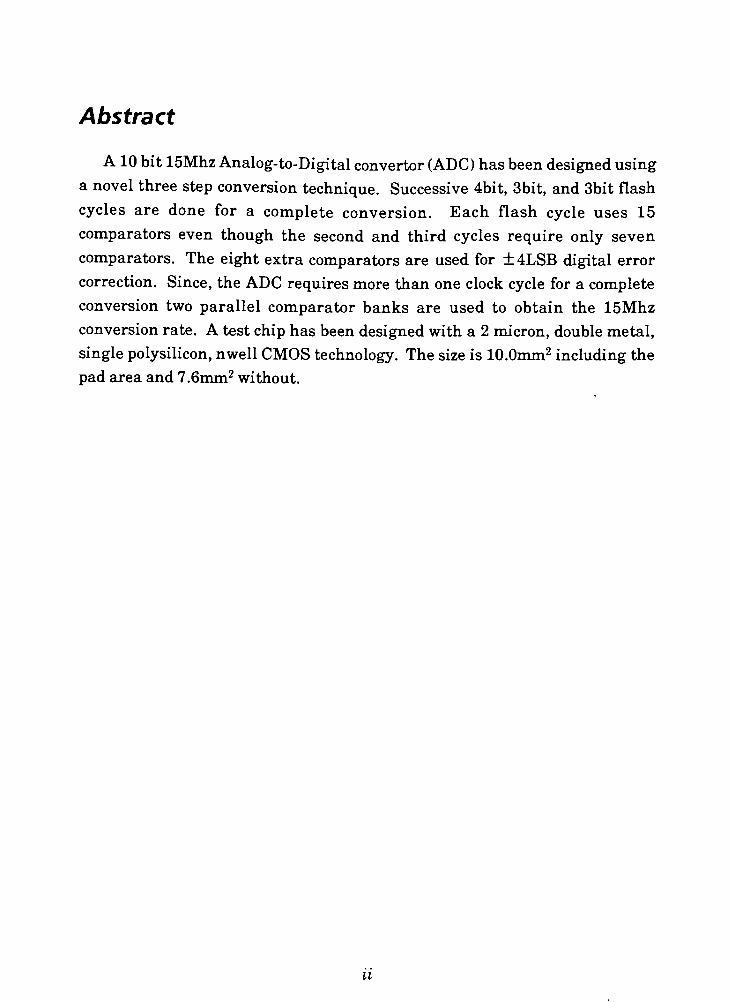
Abstract
A 10 bit 15MhzAnalog-to-Digital converter (ADC) has been designed using
a novel three step conversion technique. Successive 4bit, 3bit, and 3bit flash
cycles are done for a complete conversion. Each flash cycle uses 15
comparators even though the second and third cycles require only seven
comparators. The eight extra comparators are used for 4LSB digital error
correction. Since, the ADC requires more than one clock cycle for a complete
conversion two parallel comparator banks are used to obtain the 15Mhz
conversion rate. A test chip has been designed with a 2 micron, double metal,
single polysilicon, nwell CMOS technology. The size is 10.0mm2 including the
pad area and7.6mm2
without.
u
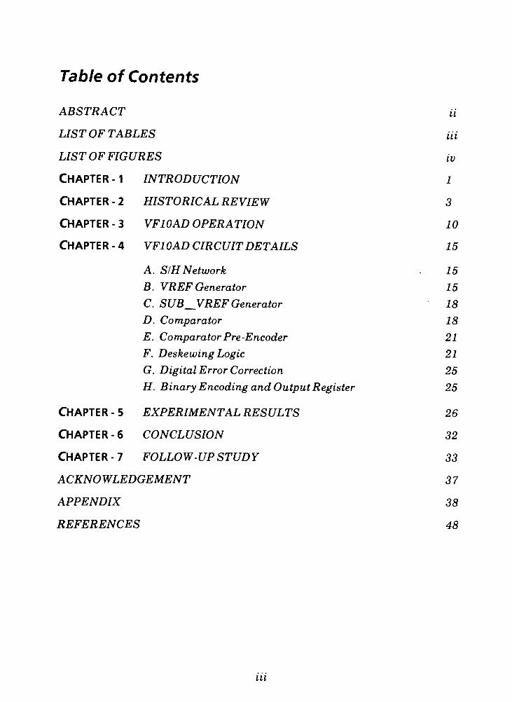
Table ofContents
ABSTRACT
LISTOF TABLES
LISTOFFIGURES
CHAPTER - 1 INTRODUCTION
HISTORICAL REVIEW
VF10AD OPERATION
VF10AD CIRCUITDETAILS
A. S/HNetwork
B. VREFGenerator
C. SUB Generator
D. Comparator
E. Comparator Pre-Encoder
F. DeskewingLogic
G. DigitalError Correction
H. BinaryEncoding and OutputRegister
CHAPTER -2
CHAPTER -3
CHAPTER -4
CHAPTER -5
CHAPTER - 6
CHAPTER -7
EXPERIMENTAL RESULTS
CONCLUSION
FOLLOW-UP STUDY
ACKNOWLEDGEMENT
APPENDIX
REFERENCES
u
Hi
iv
1
3
10
15
15
15
18
18
21
21
25
25
26
32
33
37
38
48
in
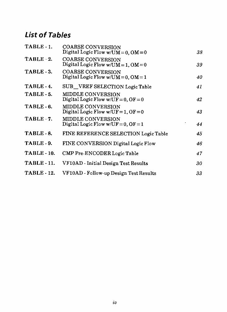
List of Tables
TABLE - 1.
TABLE 2.
TABLE - 3.
TABLE - 4.
TABLE - 5.
TABLE - 6.
TABLE 7.
TABLE - 8.
TABLE - 9.
TABLE - 10.
TABLE -11.
TABLE - 12.
COARSE CONVERSIONDigital Logic Flow w/UM= 0, OM= 0
COARSE CONVERSIONDigital Logic Flow w/UM= 1, OM= 0
COARSE CONVERSIONDigital Logic Flow w/UM= 0, OM= 1
SUB_VREF SELECTION Logic Table
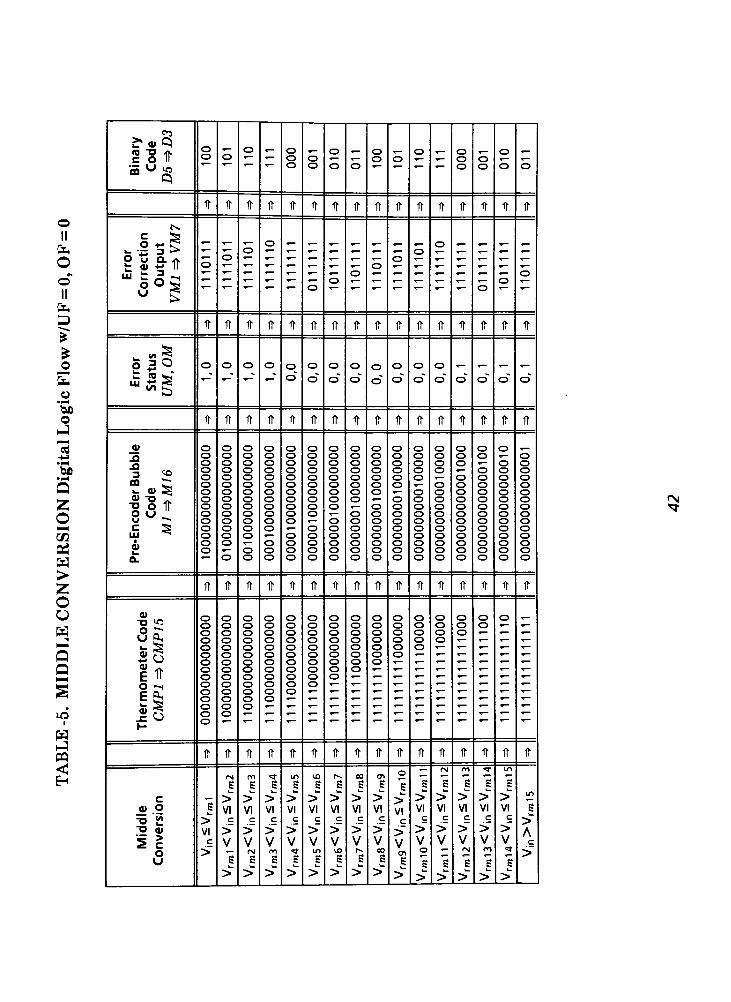
MIDDLE CONVERSIONDigital Logic Floww/UF= 0, OF= 0
MIDDLE CONVERSIONDigital Logic Floww/UF= 1, OF= 0
MIDDLE CONVERSION
Digital Logic Floww/UF= 0, OF= 1
FINE REFERENCE SELECTION Logic Table
FINE CONVERSION Digital Logic Flow
CMP Pre-ENCODER Logic Table
VF10AD - Initial Design Test Results
VF10AD - Follow-up DesignTestResults
38
39
40
41
42
43
44
45
46
47
30
33
w
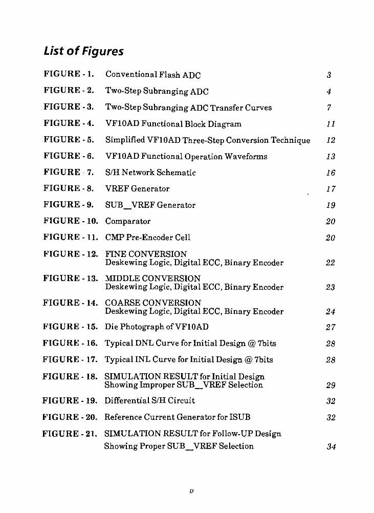
List ofFigures
FIGURE - 1. Conventional FlashADC 3
FIGURE - 2. Two-Step SubrangingADC 4
FIGURE - 3. Two-Step Subranging ADC Transfer Curves 7
FIGURE - 4. VF10AD Functional Block Diagram 1 1
FIGURE - 5. Simplified VF10AD Three-Step Conversion Technique 12
FIGURE - 6. VF10AD Functional OperationWaveforms 13
FIGURE - 7. S/H Network Schematic 1 6
FIGURE - 8. VREF Generator 1 7
FIGURE -9. SUB_VREF Generator 19
FIGURE -10. Comparator 20
FIGURE -11. CMP Pre-Encoder Cell 20
FIGURE - 12. FINE CONVERSION
Deskewing Logic, Digital ECC, Binary Encoder 22
FIGURE - 13. MIDDLE CONVERSION
Deskewing Logic, Digital ECC, Binary Encoder 23
FIGURE - 14. COARSE CONVERSION
Deskewing Logic, Digital ECC, BinaryEncoder 24
FIGURE -15. Die Photograph ofVF10AD 27
FIGURE - 16. Typical DNL Curve for Initial Design@ 7bits 28
FIGURE - 17. Typical INL Curve for Initial Design @ 7bits 28
FIGURE - 18. SIMULATION RESULT for Initial Design
Showing Improper SUB_VREF Selection 29
FIGURE -19. Differential S/H Circuit 32
FIGURE - 20. Reference CurrentGenerator for ISUB 32
FIGURE - 21. SIMULATION RESULT for Follow-UP Design
ShowingProper SUB_VREF Selection 34
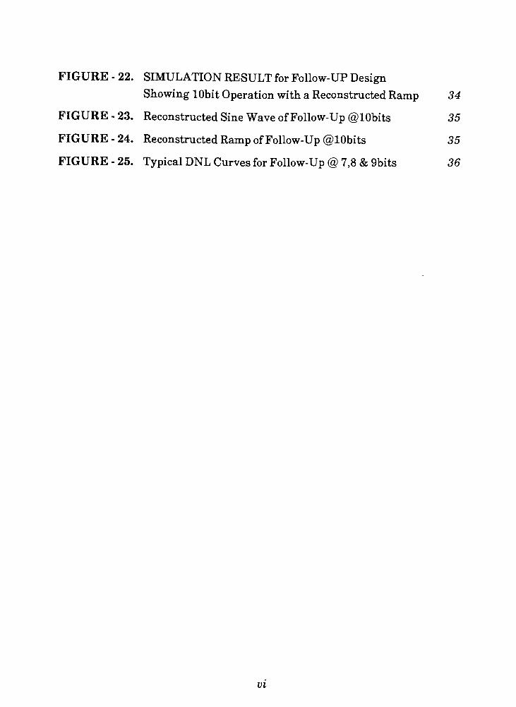
FIGURE - 22. SIMULATION RESULT for Follow-UPDesign
Showing lObit Operation with a Reconstructed Ramp 34
FIGURE - 23. Reconstructed SineWave ofFollow-Up @10bits 35
FIGURE - 24. Reconstructed Ramp ofFollow-Up@10bits 35
FIGURE -25. Typical DNL Curves for Follow-Up @ 7,8 &9bits 36
VI
Chapter - 1
Introduction
For most video frequency systems 8bits of ADC resolution is still widely
accepted. In general, the cost of the extra memory required in lObit systems
has created some inertia to keep the standard video resolution at 8bits. In
addition, advances in video processing techniques has made it possible to
increase the effective 8bit resolution by 30% or more by only converting the
active video information and stripping out the horizontal and vertical sync
signals. However, this may not be the case much longer, due mainly to the
increasing demand for HDTV. Even though the US HDTV standards are not
to be completed until 1993, several companies are anticipating the
specifications required of this evolvingADCmarket and are introducing lObit
designs capable ofconversion frequencies all the way up to 75Mhz [1, 2, 3].
The beginning of this lObit ADC evolution has been made possible mainly
because of the advances made in CMOS process technology and with the
emergence of the BiCMOS technologies. Since, the middle of the 1980's the
minimum feature size of the state-of-the-art production CMOS processes has
steadily declined from(2-3) micron to readily available (0.8-1.0) micron with
the trend continuing. Currently, submicron processes (both CMOS and
BiCMOS) (0.3-0.5) micron, are already reported to be yielding prototype
quantities ofSRAM and DRAM chip designs [4-5]. Projections have beenmade
that are based on past industry trends that predicts 0.15 micron processes will
be in use by the year 2000 [6]. Also, during the same period, the size ofwafer
diameters have increased from (2-3) inches to six inches. This represents an
increase in wafer area of (4-9)X. In fact, there is some talk in the industry to
move to eight inch and even 12 inch wafers. In addition, processes now provide
the added flexibility of commonly two and three metal interconnects and
multiple polysilicon layers (again up to 5 have been reported [7]) along with
multiple threshold transistors and precision integrated resistor and capacitor
elements. It is this combination of technology advances that has allowed the
design and fabrication of lObit ADCs.
The lObit video frequency ADC (VF10AD) that has been designed is based
on a three-step subranging conversion technique. This architecture was
developed in order to obtain a very small compact circuit that is suitable for
advanced ASIC and DSP design. It uses digital error correction with the
maximum correction capability to simplify the circuit design without
sacrificing any ADC area and power and uses pipelining to obtain the video
frequency conversion rate of 15Mhz.
Chapter - 2
Historical Review
Traditionally,monolithic video frequency (5 to 20MHz) ADCs have been by
necessity flash architecture converters [8]. A flash ADC requires 2n-l
comparators and2nmatch resistors for n bits of resolution (Fig. 1). The
2n
resistors are connected in series betweenVrt andVrb. Each resistor tap point
corresponds to an output code. The comparators are placed along the resistor
ladder at each tap point and compare Vln to Vtap. The output of the
comparator bank is a thermometer code with a"1"
to"0"
transition indicating
the location ofVrN- A true flash ADC does not have a S/H resulting in a large
input capacitance and does the entire conversion in one clock cycle making
very high speed conversion possible [9]. As the resolution of a flash ADC is
increased from n= 8bits to n = 10bits, the comparator count, resistor count,
input capacitance, area and power increase 4X. Consequently, even with the
state of the art processes that are available, the flash architecture is not the
best approach for small, low cost lObit video frequencyADC design.
To overcome the drawbacks of the flash ADC, the two-step subranging
architecture was developed (Fig. 2) [10]. The major advantage of this
architecture was that only2X(2n/2
1) comparators and2n
resistors were
required for n bits of resolution. For n= 10 this represents a 16X reduction in
the number of comparators, however, the resulting area and power savings
were obtained at the sacrifice of conversion speed. Depending on the exact
implementation there is atleast a 2X reduction in conversion speed because
multiple clock cycles were required to complete a conversion [11-14]. In
addition, the architecture by design requires a S/H with the benefit of
significantly reducing the input capacitance of the ADC making the external
drive circuits easier to design. A complete conversion with this type of ADC
architecture is done in two low resolution flash steps. The first step is the
coarse conversion it determines the MSBs while the second step is the fine
conversion and determines the LSBs. The conversion results from each step
are then combined to obtain the final higher resolution result. In the first step,
the MSB comparator bank, is connected to every2n/2
tap of the resistor ladder

FIGURE -1. Conventional Flash ADC
VRT VIN
COMPARATOR ARRAY (2n-1)
RESISTOR LADDER (2n)
Digital
Output
CLK
VIN
Digital
Output DATA(N-1) X DATA (N) )C
ThermOfneter \
AAA&r&AAA\\

FIGURE -2. Two-Step Subranging ADC
VRH
VRL
RESISTOR LADDER (2n)
^
YLSB LATCH BANK
<D &
BINARY ENCODER/DECODER
LSBs (&>
FW
=N
SUB
RANGE
ENCODERV
MSB
LATCH
BANK
&
BINARY
ENCODER/
DECODER
MSBs
<
MSB COMPARATORS (2n/2-1)
/ VIN
S/H 0
LSB COMPARATORS (2n/2-1)
1 CONVERSION CYCLE = 3 CLK CYCLES -
CLK
VIN
DATA
<D
SAMPLE
VIN (N)
<2>
MSB
COMPARATORS
SWITCHED INTO
RESISTOR TAPS
AND MSB
DECISION IS
MADE
MSB
DECISION IS
DECODED AND
LSB SUBRANGE
IS SELECTED
3>
LSB
COMPARATORS
SWITCHED INTO
RESISTOR TAPS
OF THE
SELECTED
SUBRANGE
LSB
DECISION IS
DECODED
DIGITAL
OUTPUTS ARE
UPDATED
and compared to the sampled version ofVin. The coarse conversion result is
then decoded and used to select the LSB reference voltages by performing a
D/A operation. In the second step the LSB comparator bank is connected to the
2n/2-l resistor taps between the selected reference voltages and compared to the
same Vin.
The two-step subranging architecture relies on matching of better than
+ 1LSB between the coarse conversion step and the fine conversion step for all
code transitions to avoid large nonlinearities in the output transfer curve (Fig.
3a). If the mismatch is > 1LSB missing codes will begin to appear causing
the output to no longer be monotonic (Fig. 3b). The major error sources that
contribute to the mismatch are S/H droop during the hold time, difference in
offset of MSB and LSB comparator banks, MSB decoder offset, and resistor
ladder mismatching. The matching requirements double for each additional
bit of resolution, as a result, increasing the resolution from n= 8 bits to n= 10
bits corresponds to a 4X increase.
As the resolution and the linearity requirements of ADCs increased this
subranging architecture limitation was addressed by the technique of digital
error correction. The concept behind digital error correction is to compensate
for the mismatches and not eliminate or reduce them. This is done by
expanding the size of the LSB comparator bank so that it extends into the
adjacent fine subranges by an amount equal to themaximum ( ) offset that is
expected (one comparator for each LSB of offset). The results of the expanded
comparators are then used to adjust the coarse conversion result up or down
accordingly. For example, if after the fine conversion, the thermometer code
has a"1"
to"0"
transition in the expanded area above the selected fine
subrange the MSB result is increased by one code and then added to the fine
result (Fig. 3c). However, the main drawback of using digital error correction
for a two-step ADC is having to add the extra comparators. The maximum
correction range is obtained by using2"y2
additional comparators. For n= 8
this corresponds to 16 additional comparators and for n = 10 the number
increases to 32. This represents an increase of 33% in the total number of
comparators required. Consequently, if the maximum correction range is
required by a two-step ADC then using only a digital error correction
techniquemaybe too expensive to implement due to the area required.

>
a
u
_
<
C
o>
c
(0
_a
3
xA
l/l
>
-}
u_.
<u-
l/t
c
(0
u
Q
<
c
"5>c
re_.
_Q
3t/t
Q.
i
O
sir-
00
_.
o_.
_.
V!-
0)vt
5to
3
Q
<
c
D>
C
(0-.
__
3
\U 3
\u_
U_
T A1 1 A 1Q 13 !-<-' Q-3l-Q-_5t-
-OK<-i QDh-31-
DC
(
Auu
A
t \1 1 \ 1Q
_ I -=C -0_3h---_3l- <_.-(_> l-<- O -3
1- a. z> I-
u
Q
<
c
"5c
(0_.
J_
3(/
_l
<LU
__
\
NQ (J I <_i Q-l"a-3>- -l_l !-<- 0->l---_3(-
For this reason, several new ADC circuit techniques were developed that
targeted the reduction or cancellation of comparator offset. Some of the ones
that have become"standard"
in subranging ADC design are unified
autozeroing of comparators [10], differential comparator design, and a
recycling comparator scheme [11]. Unified comparator autozeroing is used to
cancel both the offset within the comparator and the offset caused a difference
in comparator offset between the MSB and LSB comparator banks. This is
done by doing a comparator autozero at the beginning of the conversion cycle
and then using the comparator for all conversion steps simply by switching in
different reference voltages, is done only once and then used by all conversion
steps. Differential comparator design reduces and cancels induced comparator
offset by taking samples of the reference voltages and analog input at the same
time. A recycling comparator scheme is similar to the unified comparator in
that the same comparator is used for all conversion steps but is different in
that the autozero is done once for each step. Recycling does not cancel
comparator offset as well as the unified comparator but, it allows for a faster
conversion cycles because of the the comparator can operate faster. This is
because the unified comparator is always in a high gain configuration after
autozero causing the recovery time after a compare to be larger. Some
comparator saturation elimination techniques have been used [13] to reduce
the comparator recovery time. All of these techniques, although they
effectively reduce the comparator offset, also reduce the maximum conversion
frequency even more because additional clock cycles are required to the
autozeroing and recycling, however, by implementing a unified or recycling
comparator scheme the minimum number of comparators can be reduced by
1/2 to2n/2
1. For n= 8 this corresponds to 15 comparators and for n= 10, 31
comparators. This is a 50% reduction.
Finally, to increase the maximum conversion speed capable of subranging
ADCsmany now use parallel processing or pipelining [15]. The idea is to use
two or more comparator banks that are each processing a different analog
sample at the same time. Although, the number of comparators required for
the ADC is increased, the other functional blocks (resistor ladder, decoders,
output register, and clock generation) can all be shared with a minimal
8
amount of overhead. The tradeoff can be made between power and speed
depending on the circuit requirements.
To summarize, the flash ADC architecture is not appropriate for low cost
lObit video frequency convertors because of the number of comparators
required. The two-step subranging ADC architecture evolved mainly as a
vehicle to reduce the number of comparators by up to 16X, however, the basic
circuit performance is limited by the matching between the conversion steps.
For this reason, the digital error correction technique was developed. It
however, is too costlywhen implemented withmaximum correction capability,
which is more than likely needed at lObit resolution. For lObits this
represents 32 additional comparators. As a result, new offset cancelling
techniques emerged that reduce the impact ofdigital error correction but, they
also reduce the maximum because of the additional clock cycle overhead.
Finally, to increase the conversion speed parallel processing or pipelining is
used at the penalty of atleast 2X number of comparators but with minimal
additional silicon overhead. Many different ADC architectures continue to be
reported that are based on the concepts that have been discussed, however,
none use themaximum digital error correction capability due to the number of
comparators required. The VF10AD test chip that has been designed is one of
these architectures, however, the algorithm it uses employs maximum digital
error correction capability without the penalty of the additional comparators.
This is done by using a three step conversion scheme of 4,3, and 3bit steps
instead of two. The details ofwhich follow.
Chapter - 3
VF10AD Operation
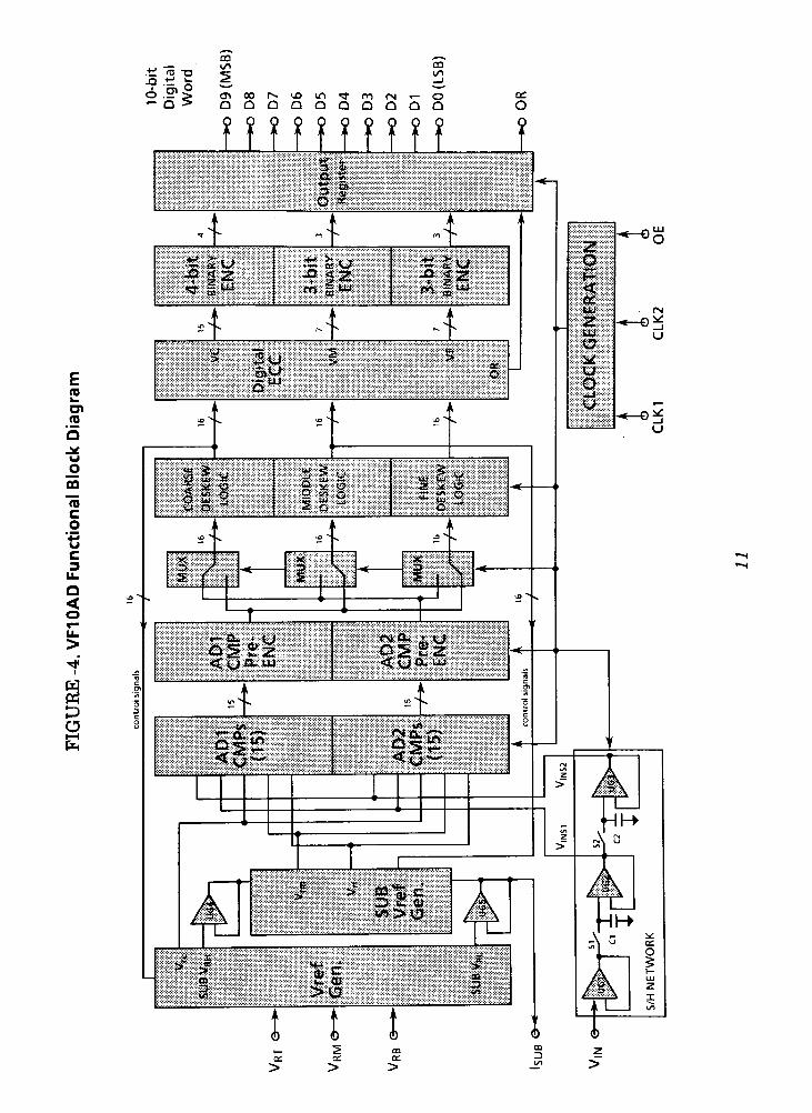
The VF10AD (Fig. 4) will convert all analog input voltages (Vin) that are
within the conversion limits (Vrt- and VrbO established by the external
reference voltages, Vrt and Vrm. Any Vin that is beyond these () is
considered out-of-range and the digital outputword (D9-D0) will remain at full
scale (ie. all l's ifVin>Vrt' or all O's ifVin<Vrb*). IfVin is withinVrt' and
Vrb' the ADC will convert it to an equivalent lObit digital output word in
three subranging conversion steps (Fig. 5). The first subranging step, or
COARSE conversion, determines the four MSBs, D9-D6. The second
subranging step, or the MIDDLE conversion, determines D5-D3. The third
and final subranging step, or FINE conversion, determines the three LSBs,
D2-D0. In order to increase the conversion rate, VF10AD, has two parallel
ADCs, AD1 and AD2, operating in a pipelined manner. However, the only
circuits that are actually duplicated are the comparator and pre-encoder. This
is possible because of the way the conversion cycles for each ADC are pipelined
(Fig. 6).
A conversion cycle for either AD1 or AD2 begins with the comparators
sampling Vinsi and the coarse reference voltages, Vrc(i_i5), simultaneously.
The differential voltage (ViNSl-Vrc(l-15)) is amplified and the coarse
conversion is achieved (Table 1). The conversion results are pre-encoded to
generate the control signals which select the conversion limits for the middle
conversion, SUB Vrh and SUB Vrl, (Table 4) and are alsomultiplexed into
the coarse deskewing logic. Next, the subrange reference generator generates
15 reference voltages, Vrm(i-i5), between SUB_Vrh and SUB_Vrl. These
voltages along with VinS2 are again sampled simultaneously by the same
ADC comparator that was used for the coarse conversion. The differential
voltage (ViNS2-Vrm(l-15)) is then amplified and the middle conversion is
achieved (Table 5). The middle conversion is pre-encoded to generate the
control signals that select the fine reference voltages, Vrf(i-i5) (Table 8), and
are also multiplexed into the middle deskewing logic. Since, the middle
conversion is a 3bit operation, only seven reference voltages are required. The
10
aa
01o >o >
o ^
WOONlfllll'JfilN'-O
____________________
f Y f f f f H f ? Y
Ere_.
o>
re
w
co
"rec
o
'^w
c
3U.
Q
<o
>
Oii

3+>
W
0>
<c
o
"3!
>
c
o
u
Q.
vn
V
V_.
_c
r-
Q
<o
LO _"> m rsi
VV^VKh-VA^Aa^Vas r~
LL. U_
c_ 0_
lo -"
^"
m <N
U_ LL. LL. LL. Ll_ U_
_________
to rr>
_00
<M
u- >.__
ou
o
a.
E
ID
oII
o_
>
__Vj_VL. . .j-vtW^-~*W-
u
0_ Q_
uQ_ J
o_
c_
>
ID
U
Q_
UQ_
U
0_
'
O -Q
u **in -o
.
Q_ 0_ L_>
<(LU
o > s-
u __o
TO-
u

o
01
a.
u
>.
u
c
o
Oi
>
c
ou
I/I
E
00
__
-J
u
CM
__
-_
<
rN
Q
<<
eight extra voltages are used for digital error detection and correction. The
middle conversion can correct for up to 128mV (equal to4LSB @6bits
resolution) of offset relative to the coarse conversion. In the third and final
conversion step Vrf(i-i5) and VinS2 are sampled simultaneously by the same
comparator used for the coarse andmiddle conversions, the differential voltage
(ViNS2-Vrf(i-i5)) amplified, and the fine conversion achieved (Table 9). The
fine conversion (like the middle) is also a 3bit operation and once again the
extra reference voltages are used for digital error detection and correction.
The fine conversion can correct for up to 8mV (equal to 4LSB @10bits
resolution) of offset relative to the middle conversion. The fine conversion
results are pre-encoded and multiplexed into the fine deskewing logic. After
the deskewing logic digital error correction and binary decoding are done and
the digital output word, D9-D0, is transferred to the output registerand the
conversion complete.
14

Chapter - 4
VF10AD Circuit Description
A. SIH NETWORK
This section consists of three unity gain buffers, UG1-UG3, and two S/H
circuits (Fig. 7). The analog input voltage, Vin, is buffered by UG1, then
sampled by SI and held on Cl, buffered byUG2, sampled by S2 and held on C2,
and finally buffered again by UG3. The output voltage of UG2, Vinsi, is
connected to the coarse sampling input of the AD1 and AD2 comparators. The
output voltage of UG3, VinS2, is connected to both the middle and fine
sampling inputs of the AD1 and AD2 comparators. UG1-UG3 are two stage
opamps connected in the unity gain configuration. The S/H circuits (S1,C1
and S2,C2) are connected in series in order to take advantage of the error
correction circuit between the coarse and middle conversion steps and reduce
the matching requirements ofVinsi and VinS2- The switches, SI and S2, use
dummy switches to reduce the sample to hold step in Vinsi and VinS2- This
minimizes the offset betweenVinsi and VinS2 and allows both the middle and
fine conversions to sample VinS2- The hold capacitors, Cl and C2, are really
two capacitors of half value on each side of the sample switches. This allows
the channel charge to divide equally between the source and the drain of the
sample switchesminimizing the variability of the S/H step ofVinsi andVinS2-
B. VREF GENERATOR
This section consists of 18 resistors (Rc(l-18))> two unity gain buffers (UG4
andUG5), and 32 nmos switches (Fig. 8). The resistors are connected between
the external reference voltages, Vrt and Vrb, to generate the coarse
conversion reference voltages, Vrc(i-i5), and middle conversion's limits
SUB Vrh and SUB Vr_. Vrb is connected to the bottom of the first resistor
and Vrt connected to the top of the 18th resistor. The center tap of the
generator can be connected to a voltage equal to (Vrt-Vrb)/2+Vrb if it is
necessary to reduce integral nonlinearity (INL). Vrc(i-i5) are obtained by
tapping the generator between at Rc(i) and Rc(i+ 1) where i= 1-15. SUB_Vrh
is obtained from a 16 to 1 multiplex ofVrc(i), where i = 2-17 andSUB_Vrl from
15

o__
LU
>
<
<__
oI-
u
re
EXV
_c
_>
</l
._-
13
Oi i
En
I
\
\
\
\
S
>
CO
cm
II
c
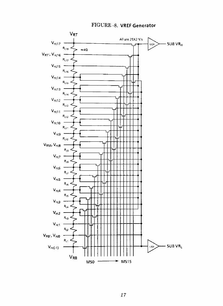
FIGURE -8. VREF Generator
Vrt
v rc17
Vrt. Vrci6
Vrc15
'rc14
Vrc13
'rc12
Vrc11
Vrc10
'rc9
VRM- Vrc8
'rc7
Vrc6
'rc5
Vrc4
Vrc3
'rc2
VrC1
Vrb', Vrc0
Vrc(-1)
All are 25X2N'
s
Rcl8 <;> _,4Q
~L_r
J U
RC17 <-~>
_r
Rc16 "^A.
L.J
r LJ
j
T
RC15 ^A L
[ L_l
JRc14 *~^>
L X
r l_J
T
Rc13 <~AL J
r LJ
t
Rc12 "^"-^L J
r~
LJ
T
RC11 ^""^L J
r LJ
IRc10 <~^>
L J
f~
U_l
JRc9 P^
L J
f L,J
JRC8 "^^y.
L J
jLJ
T
RC7 <~p>L J
f~
_.-1
J
Rc6<>L J
jLJ
T
Rcs*^L J
[ LJ
T
RC4 *""->
i J
L J
"]J
L J
Rc2 <L
L J
Rcl <
L J
V| _
L J
ug4^> SUB VRH
SUBVR,
MSO MS15
17
a 16 to 1 multiplex ofVrc(i), where i = (-l)-14. SUB_Vrh and SUB_Vrl are
buffered byUG4 and UG5 so that the SUB_VREFGENERATOR does not load
the VREF GENERATOR. The pre-encoded coarse conversion result is used as
the muxxing control signals to the 32 switches (Table 4). UG4 and UG5 are
two stage opamps with an output stage connected in the unity gain
configuration.
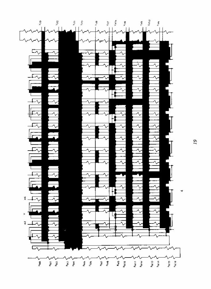
C SUB_VREF GENERATOR
This section consists of 192 resistors (4_ each) Rm(1-192) and 16 banks of 15
nmos switches (Fig. 9). The resistors are connected between SUB Vrh and
SUB Vrl from the vref generator and generates the middle and fine
conversion's reference voltages, Vrm(i-i5) andVrf(i-i5). SUB Vrl is connected
to the bottom of the first resistor, Rmi, while SUB Vrh is connected to the top
resistor Rmi92- A constant but adjustable current, IsuB, is pulled from from
the resistor ladder at SUB Vrl so that the offset of UG5 is equal to that of
UG4. IsuB is nominally set equal to 2XIsuBVREF> however, it can be adjusted
up or down in order to match the offsets of UG4 and UG5. Vrm(i_i5) are
obtained by tapping the voltage divider between Rm(32+ 8D and Rm(33 + 8_)>
where i = 1-15. Vrf(i-i5) are selected by exercising 1 of 16 banks of switches
that are connected to the generator between Rm29 and Rmi63- If
Vrm(i)<ViN<=Vrm(i+ i) then, Vrf(j) =RM(28+8i+i), where i = 1-15 andj = 1-15.
The pre-encoded middle conversion results are used as the muxxing control
signals to select the correct switch bank (Table 5).
D. COMPARATOR
The VF10AD has a total of only 30 comparators (CMP). This compares to
1023 that are required for a full flash ADC and 126 for a two step half flash or
subrangingADC. Each CMP is a recycling (ie. the same comparator is used for
all conversion steps) differential circuit consisting of a sampling stage, a
positive feedback gain stage, and a latching circuit (Fig. 10). The CMPs are
reset (ie. offset is cancelled) each conversion step by sampling Vin and a
reference voltage simultaneously (Vrc, Vrm, or Vrf), storing the values on the
input gates of the gain stage while it is in a low gain condition. The
comparison is made by enabling the positive feedback and amplifying the
difference between the two input voltages. IfVin >(Vrc, Vrm, orVrf) the CMP
18
O}

FIGURE -10. AD1 and AD2 Comparator
A|N
T
P1 \
REF
IT
P2\
A
P3
\
"I
A
P3
SAMPLE STEP - PI is open. P2 & P3 are closed
COMPARE STEP- P1 is closed, P2&P3 are openi
Out
DFFQ_ Q
DFF Q- Q*
FIGURE -11. CMP Pre-Encoder Cell (AD1 and AD2)
clkF
c\kH
clkE
clkG
ZD
Clock for AD1
Clock forAD2ClkG
c\kF(refer to CLOCK GENERATION
Logic Diagram)
T^O-P^O- C0-C15 (to Coarse Deskewing Logic)
__T^>Q(j>0 MO-M 1 5 (to Middle Deskewing Logic)
rT___r"Nor^o~~ po-F ! s (t Fine Deskewin9 L9ii:'
Node Name
A N
B (N-1)*
N and (N-1 ) referto CMP(N) and CMP(N-1)
20
outputs a digital "1". If Vin < (Vrc, Vrm, or Vrf) the output is a "0". The
comparator output is then stored in the latch circuit while the CMP is reset for
the next conversion step.
The CMPs are divided into two parallel banks of 15 CMPs each. One bank
is for AD1 and the other for AD2. The output vector from each comparator
bank is a thermometer code. That is, for every CMP with Vr(C)m, or f) > = Vin
the output is"1"
while all others are "0". AD1 and AD2 share the same vref
and sub-vrefgenerators, deskewing logic, binary encoder, error correction, and
output register. They, however, require separate pre-encoders because of the
way the coarse and fine conversion cycles overlap. The CMP arrays for the
middle and fine conversions have been expanded from seven to 15. The extra
CMPs are used for digital error correction. The CMP banks for AD1 and AD2
are also integrated in the layout in order tominimize their contribution to any
offset between AD1 and AD2.
E. COMPARATOR PRE-ENCODER
The comparator pre-encoder consists of 32 nor gates that are divided into
two banks of 16 each (Fig. 11). One bank is for AD1 and the other for AD2.
The encoder banks detect the"l-to-0"
crossing in the thermometer code of the
driving CMP bank for each step of the conversion cycle. The encoder output is
converted into a bubble vector of all "0"s and a single"1"
corresponding to the
"l-to-0"
crossing (Table 10). The encoding is done by comparing the results of
theNth and the (N-1) CMPs. IfCMP(N-l) ="1"
and CMP(N)="0"
the encoder
outputs a "1", otherwise the output is a "0". The outputs of the encoder banks
are thenmultiplexed into the deskewing logic coarse,middle, or fine.
F. DESKEWING LOGIC
The purpose of the deskewing logic is to provide a digital delay in the data
path ofeach conversion step so that the complete conversion is processed by the
digital error correction and binary encoder circuits at the same time. This
circuit consists entirely of clocked D flip flops. The coarse deskewing logic is
three registerswide, themiddle two and the fine one (Fig.'s 12, 13 and 14).
21
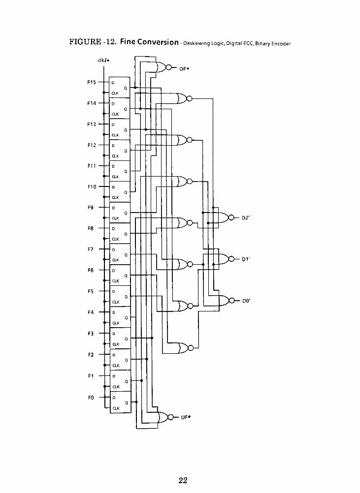
FIGURE -12. Fine Conversion -
Deskewing Logic, Digital ECC, Binary Encoder
JO-DO"
22

13. Middle ConverSJOn - Deskewing Logic, Digital ECC, Binary Encoder
M15
M14
M13
M12
M11
M10
M9
M8
M7
M6
M5
M4
M3
M2
M1
MO
FINE REF. SELECTSUM*
23

FIGURE -14. Coarse Conversion Deskew ing Logic, Digital ECC, Binary Encoder
MIDDLE REF. SELECTSUM*
C15
C14
C13
C12
C11
C10
C9
C8
C7
C6
C5
C4
C3
C2
C1
CO
MIDDLE REF. SELECTS
UM*
24
G. DIGITAL ERROR CORRECTION
The VF10AD uses digital error correction to correct for some of the ADC
nonidealities. This circuit corrects for the offset voltages that will exist
between the coarse and middle conversion steps and between the middle and
fine conversion steps. This is done by expanding the number ofCMPs used by
the middle and fine conversions from the seven required for a 3bit conversion
to 15. The eight extra CMPs expand into the adjacent middle and fine
conversion ranges by four CMPs. If an error condition occurs the CMP
thermometer code will have a"l-to-0"
transition somewhere in this expanded
area. There are two possible error conditions, over-range and under-range.
Over-range is the condition when the present conversion step (middle or fine)
determines that Vin is above the conversion range that was selected by the
previous conversion step (coarse ormiddle). Under-range is the exact opposite.
After the conversion cycle is complete the out-of-range bits from the fine
conversion, UF and OF,"ripple"
back to the middle conversion. The middle
conversion is then adjusted up or down if necessary depending on whether an
over-range (OF = 1, Table 6) or an under-range (UF = 1, Table 7) condition has
occurred. The middle conversion out-of-range bits, UM and OM, are then set
or reset and transferred to the coarse conversion. The coarse conversion
results are then also adjusted accordingly (Table 2 and 3) and the out-of-range
bits, UFLOW and OFLOW are set or reset. If the coarse over-range bit is set
(OFLOW= 1) then an overflow condition was detected (ie. Vln>VrtO or if the
under-range bit is set (UFLOW= 1) an underflow condition was detected (ie.
Vin<Vrb').
H. BINARY ENCODING and OUTPUTREGISTER
The binary encoder converts the digital error corrected data to a binary
coding using nine eight input nand gates (Fig.'s 12, 13 and 14). If the overflow
bit is set, OFLOW= 1, the encoder sets the digital word to full scale of al "l"s.
If the underflow bit is set, UFLOW = 1, the digital word is reset to full scale of
all "0"s. The digital output register is a bank of 10 one bit latch circuits with a
tristateable CMOS level output driver.
25
Chapter - 5
Experimental Results
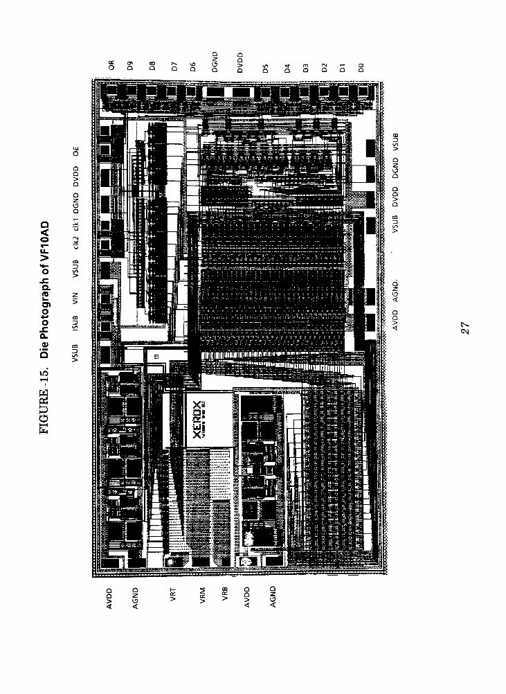
The prototype lObit video frequency ADC, VF10AD, that has been
described was implemented using a single polysilicon, double metal, nwell,
2.0um CMOS process. The die size is approximately10.0mm2
including the
pad I/O and7.6mm2
without it. It dissipates around 410mW at 7.5MHz from a
single 5V supply. A photo of the die is shown in Figure 15. The ADC contains
approximately 4000 transistors.
During testing and debug the VF10AD was found to have typical
performance curves as is shown in Figures 16 and 17. Only 7bits of the lObits
were found to be fully functioning over the entire analog input range, however,
all lObits were found to be functioning for the lower l/16th of the same
conversion range. Outside of this range, the lower three LSBs are stuck in the
"011"
overrange condition. It was discovered that SUB Vrh and SUB Vrl
were being incorrectly updated during the fine conversion cycle sample
operation, causing the lowest sub reference section to be sampled every
conversion cycle resulting in an over-range condition. Chip level simulations
confirm this (Fig. 18). The conversion speed of the VF10AD is being limited to
7.5MHz because there is a slew rate difference at the output ofUG4 and UG5
(from SUB VREF Generator) that is causing a gain error to exist between the
coarse and middle conversions as the rate is increased above 7.5MHz resulting
in missing codes. The cause of the slew difference is the additional loading
(approximately lOpF) on SUB Vrl due to the IsUB probe. If IsuB was not
required, the conversion rate would be limited to approximately 10MHz still
less than the goal of 15MHz. This is because the slew rate of UG4 was
measured to be 0.8V/ns about 25% less than the lV/ns (UG5 is worse due to
ISUB) that is required for 15MHz operation. Also, the S/H step ofVinS2 was
found to vary from 5mV to +8mV over the analog input range. This is on
the edge of themiddle to fine conversion correction range and will likely result
in nonlinearities at the lObit level but at the 7bit level it is not a factor because
one LSB is equal to 16mV. The DC characteristics ofUG(l-5) were measured
and found to have a gain of 0.999X and an offset of < lmV over the analog
26
a
a>
Q
Q
z
XD
a
,_
Q __
<o
rsl
__
^~
u.
>m
H- r>
o>
Q.to Z
O)>
O+> m
o _3
_:
(/l
a.
XV m
a_D
v>
r>.
CN
?>
<
Q
Z<_>
<
o_
>0_
>
0
>
Q
Q
>
< <

FIGURE -16. Typical DNL Curve for Initial Design @ 7bits
L
S
B
-0.5
CODE (0-127)
FIGURE -17. Typical INL Curve for Initial Design @ 7bits
L
S
B
-0.5
CODE (0-127)
28

FIGURE -18. Simulation Result Showing Improper SUB_VREF Selection
W/ TLZ^D
'. Scooe **;
_:x.r
29
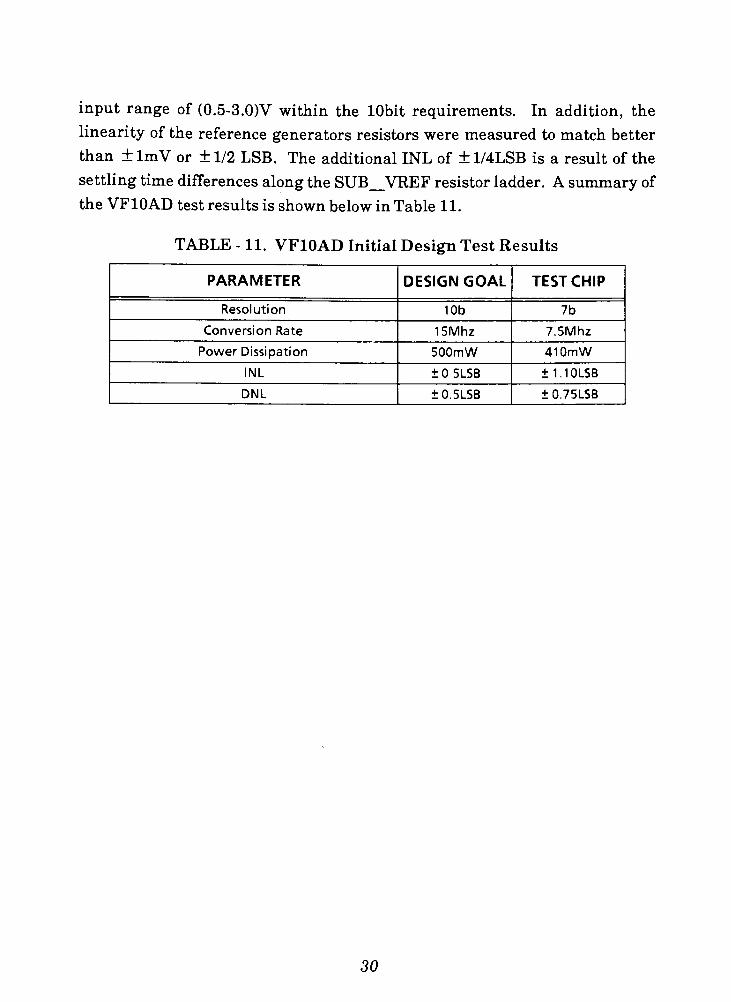
input range of (0.5-3.0)V within the lObit requirements. In addition, the
linearity of the reference generators resistors were measured to match better
than lmV or 1/2 LSB. The additional INL of 1/4LSB is a result of the
settling time differences along the SUB_VREF resistor ladder. A summary of
the VF10AD test results is shown below in Table 11.
TABLE - 11. VF10AD Initial Design Test Results
PARAMETER DESIGN GOAL TEST CHIP
Resolution 10b 7b
Conversion Rate 15Mhz 7.5Mhz
Power Dissipation 500mW 410mW
INL 0.5LSB 1.1 OLSB
DNL + 0.5LSB 0.75LSB
30
Chapter - 6
Conclusion
Even though the VF10AD did not function 100% as was intended the
experimental results that were able to be obtained confirm the feasibility of
the conversion technique, however, there are some design improvements that
should bemade. First, the magnitude of the S/H step has to be reduced so that
it does not use the entire fine to middle conversion correction range. The best
method to accomplish this is to use a differential sampling circuit like in
Figure 19. Themajor advantage of this circuit is that the S/H step is virtually
eliminated by making it a common mode signal. There will be some residual
left due to the finite common mode gain of the opamp and small differences in
the hold step of the sample switches. Second, the IsuB loading affect should be
removed. This could be done using IsuB to bias an on-chip current source that
would provide the pull down for the SUB VREF generator as shown in Figure
20. Third, the power of the reference ladder has to be optimized for 15MHz
operation to reduce the power dissipation. It presently, dissipates 60mW of
power, an over design.
The 15Mhz conversion speed will be obtainable by increasing the
bandwidth of UG(l-5) and eliminating the extra SUB Vrl loading due to
ISUB- The bandwidth increase could be easily done by doing a redesign at
submicron design rules instead of the 2 micron rules used or by using the brute
force approach of using more power (not the desired path). Also, based on the
laddermeasurements the INL of the VF10AD is not expected to be < 1/2LSB,
however, if the quarter tap points of the reference generator are made external
or if amethod ofselfcalibration was used 1/2 LSBmay be possible.
31
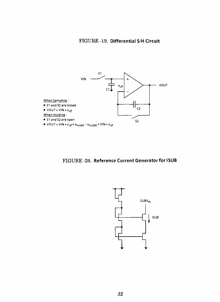
FIGURE -19. Differential S/H Circuit
VIN
When Sampling :
S1 and S2 are closed
VOUT = VIN + uoff
When Holding :
S1 and S2 are open
VOUT = VIN + vofr+ vholdsl-
vholdS2= VIN + voff
VOUT
FIGURE -20. Reference CurrentGenerator for ISUB
SUBVRL
ISUB
32
Chapter - 7
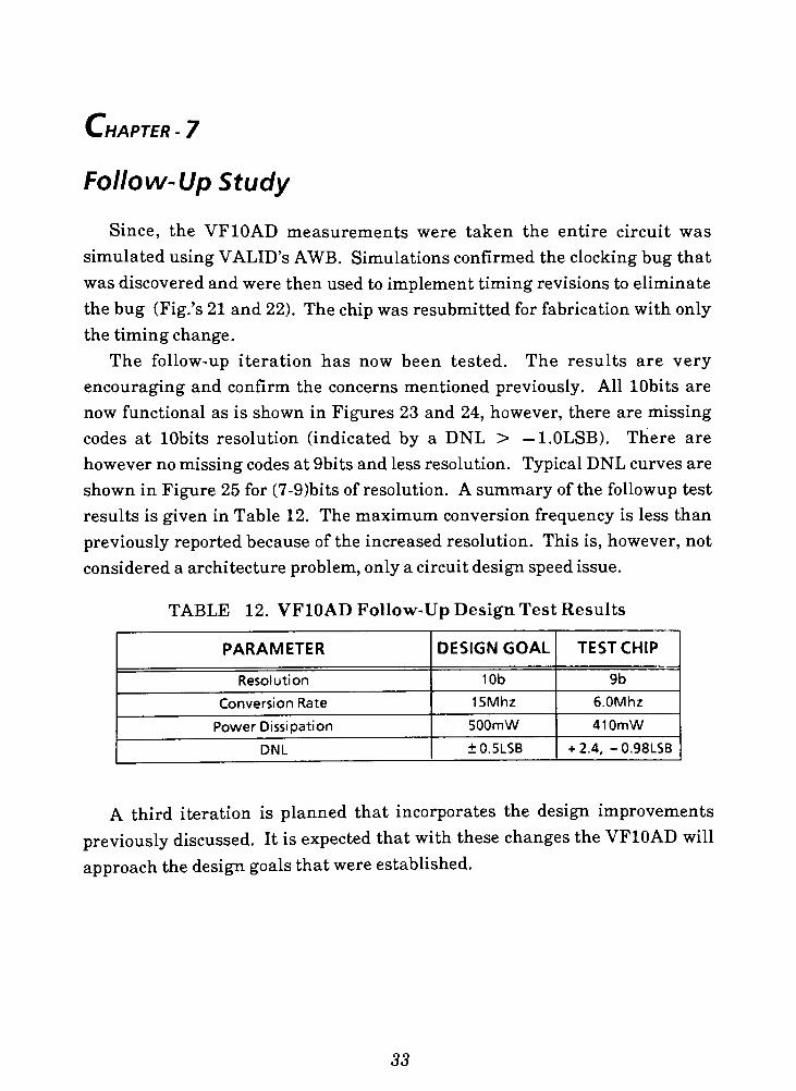
Follow-Up Study
Since, the VF10AD measurements were taken the entire circuit was
simulated using VALID's AWB. Simulations confirmed the clocking bug that
was discovered and were then used to implement timing revisions to eliminate
the bug (Fig.'s 21 and 22). The chip was resubmitted for fabrication with only
the timing change.
The follow-up iteration has now been tested. The results are very
encouraging and confirm the concerns mentioned previously. All lObits are
now functional as is shown in Figures 23 and 24, however, there are missing
codes at lObits resolution (indicated by a DNL > 1.0LSB). There are
however nomissing codes at 9bits and less resolution. Typical DNL curves are
shown in Figure 25 for (7-9)bits of resolution. A summary of the followup test
results is given in Table 12. The maximum conversion frequency is less than
previously reported because of the increased resolution. This is, however, not
considered a architecture problem, only a circuit design speed issue.
TABLE 12. VF10AD Follow-Up Design Test Results
PARAMETER DESIGN GOAL TEST CHIP
Resolution 10b 9b
Conversion Rate 15Mhz 6.0Mhz
Power Dissipation 500mW 410mW
DNL 0.5LSB + 2.4, - 0.98LSB
A third iteration is planned that incorporates the design improvements
previously discussed. It is expected thatwith these changes the VF10AD will
approach the design goals that were established.
33

FIGURE -21. Simulation Result Showing Proper SUB_Vref Operation
-_=T
Jm7t -.<,.: cscod.'TLnPD
| " a_ ,, | _.-..w
-
Ma
*"" 17 j
/:
A
Cl
FIGURE -22. Simulation Result of Reconstructed Ramp @ lObits
mi!/Cad l_.p.. ,ri2flD
,. 1 1 --, ._,. --.*-, 1 J<.l.t
^_j_ . __= ___
'
r"
v
!h
V
.S-ODB 9Bt j ON
,
IN
2 3c_oa 5-,
OFT'
Sua
; OFT SUEL
I ^m , a ,.
Func uai.
34
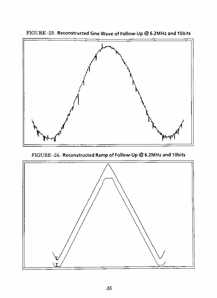
FIGURE -23. Reconstructed Sine Wave of Follow-Up @ 6.2MHz and lObits
FIGURE -24. Reconstructed Ramp of Follow-Up @ 6.2MHz and lObits
35
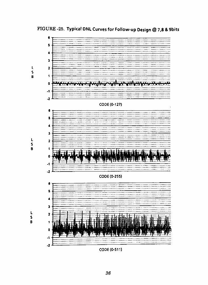
FIGURE -25. Typical DNL Curves for Follow-up Design @ 7.8 & 9bits
L
S
B
L
S
B
L
S
B
'rWjji&xfc^^
CODE (0-127)
CODE (0-255)
_eSifWiTFWiirilFHWilfllllFiWI'iiinnWSWsilljpi'ivr
CODE (0-511)
36
Acknowledgements
I would like to thank XEROX Corp. for fabricating the VF10AD, Mike E.
Colling for doing the probe card layout, Fred O. Hayes for doing the probe card
circuit design and test software, and David J. Metcalfe for comparator design
consultation.
37

c
a
O
VpH
_)
o
CS
be
Q
o
>zo<_
Hgg
O
(J
o
oo
o
o
oo
o
o
oo
o
o
o
o
o
o
o
o o
o
o
o
o
o
o
o o
oo o
o -
ft ft ft ft ft ft ft ft ft ft ft ft ft ft ft ft
=
o
oo
ft ft ft ft ft ft ft ft ft ft ft ft ft ft ft ft
o
<3
o o
o
o o o o o o
o
o
o
o o o o o o
ft ft ft ft ft ft ft ft ft ft ft ft ft ft ft ft
o
o
oo
o
o
o
ooo
o
o
o
oo
o
oo
o
o
ooo
o
o
o
o
oo
o
o
o
o
o
oo
o
o
o
o
o
oo
o
o
oo
o
o
oo
o
o
o
oo
o
o
o
o
oo
o
o
oo
o
o
o
oo
o
o
oo
o
oo
o
oo
o
o
o
o
o
oooo
ooo
o
oo
o
o
o
o
o
oooo
o
oo
o
oo
o
o
oo
ooo
o
o
o
oo
o
oo
o
oo
o
o
oo
o
o
o
oo
o
oo
ooo
o
oo
o
o
o
ooo
o
o
ooo
o
oo
o
o
oo
o
ooo
o
ooo
o
oo
o
oo
o
oo
o
o
ooo
o
o
oo
o
o
oo
o
o
o
o
o
oo
o
oo
o
o
oo
o
o
o
o
o
oo
ooooo
o
oo
o
oo
o
o
oo
o
o
oo
o
oo
o
o
ft ft ft ft ft ft ft ft ft ft ft ft ft ft ft ft
=>
ooooooooooooooo
o
o
o
o
o
o
o
o
o
ooooo
o
oooooooooooo
ooo
ooo
o
o
oo
o
o
o
o
o
o
o
o
o
o
o
o
o
o
oo
ooooo
oo
o
ooooooo
o
ooooo
o
o
o
oo
o
oo
o
o
o
o
o
o
o
o
o
oooo
oooo
o
oo
o
o
o
^~
ft ft ft ft ft ft ft ft ft ft ft ft ft ft ft ft
>
VIc
>
CM
>
VIc
>
V
u
>
m
>
VIc
>
VCMo
>
"3-
<y
>
VI
c
>
Vm
>
ino
>
VIc
>
V"3-
<_
>
u
>
VIc
>
Vin
>
u
>
VIc
>
V
u
>
CO
>
VIc
>
V
>
<_n
>
VIc
>
VCOu
>
o
-
>
VI
>
V
>
>
VIc
>
Vo
t_>
>
fNJ
>
VIc
>
V
_
>
m
<y-_
>
VIc
>
V
<_
>
a-
-
>
VIc
>
Vm
ut_-
>
m
o1
>
VIc
>
V
_
>
in
o
>
Ac
>
00

o
5
JO
beo
be
5
Oii
GO
>
oo
wGO
<oo
w
E-i
o
o
o
o
o
o
oo
ooo
o
o
oo
o
o
o
o
o
o
o
o o
o
oo
o
o
o
o o
o
o o
o
ft ft li ft li ft ft ft ft ft ft ft ft ft ft ft
oo
ft ft ft ft ft ft ft ft ft ft ft ft ft ft ft ft
o o o
o
o
o
o o
o
o
cT
o
<_
o
o
o o o o o o
o
o
ft ft ft ft ft ft ft ft ft ft ft ft ft ft ft ft
oo
o
oooo
o
ooooo
o
o
o
o
o
ooo
oooooo
o
o
o
o
o
ooo
ooooo
ooo
oo
ooo
o
oooo
oooo
o
oo
oo
o
o
oo
o
ooo
o
oooo
oo
o
ooo
oooo
o
oo
o
o
oo
o
oo
o
ooo
o
oo
o
o
o
oo
o
ooo
oo
o
o
o
oo
o
o
o
oo
oo
o
o
o
oo
oo
o
o
o
o
oo
ooo
o
o
o
oo
o
o
oo
oo
oo
o
oo
o
oo
oo
o
oo
o
o
o
o
o
oo
o
ooo
o
o
oo
o
o
o
o
o
oo
o
oo
o
o
ooo
o
o
o
o
oo
o
o
oo
o
o
oo
o
o
oo
oo
o
oo
o
oo
oo
oo
o
o
oo
o
o
oo
oo
o
o
o
oo
ft ft ft ft ft ft ft ft ft ft ft ft ft ft ft ft
=*
o
ooooooooooooo
o
o
oo
oo
o
o
o
oooo
o
o
oo
oo
o
o
o
o
o
o
o
o
o
oooooooooooo
o
o
o
o
oo
o
o
ooo
o
oo
oooo
o
o
o
oooo
o
o
o
o
o
oo
o
o
o
o
o
o
oo
o
o
o
oo
o
ooooo
o
o
ooo
oooo
ooo
o
o
o
-
ft ft ft ft ft ft ft ft ft ft ft ft ft ft ft ft
_
>
VIc
>
_
>
VIc
>
V
u
>
m
>
VIc
>
V
>
_
>
VIc
>
Vco
>
in
>
VIc
>
V<*u
>
>
VIc
>
Vm
>
o
>
VIc
>
V
u
>
COo
>
VIc
>
V
o
>
>
VIc
>
VCO
>
o
>
VIc
>
V
o
>
>
VIc
>
Vo
_
>
("SI
_
>
VIc
>
V
>
on
o
>
VIc
>
V
__
>
>
VIc
>
Vm
u
>
in
u
>
VIc
>
V
>
m
o
>
Ac
>
en
2o
o
SupH
beo
-*_
bo
Q
ZohI
GO
tfH
>
o
<oo
CO
W
pq
<*
o
o
o
o
o
ooo
oo
o
o
o
o
o o
o
o
o
o
o
o
o o
o
o o
o --
ft ft ft ft ft ft ft ft ft ft ft ft ft ft ft ft
=>
o
o
oo o
ft ft ft ft ft ft ft ft ft ft ft ft ft ft ft ft
o
o
o o
o
o
o
o o o o o o o o o o o
ft ft ft ft ft ft ft ft ft ft ft ft ft ft ft ft
=>
o
o
oo
o
o
o
oooo
o
o
o
o
o
ooo
o
o
oo
oo
o
o
oo
o
oo
o
o
o
oo
o
o
oo
oo
oo
o
o
o
o
oo
o
o
o
ooo
o
o
o
o
o
oo
o
o
o
o
ooo
o
ooo
o
o
oo
o
o
ooo
o
ooo
o
o
o
o
oo
o
o
oo
o
oooo
o
o
o
o
oo
o
o
oo
o
oo
o
o
oo
oo
o
oo
o
o
o
o
ooo
ooo
oo
o
oo
o
oo
o
ooo
o
o
o.
oo
o
oo
ooo
oooo
o
oo
o
o
oo
o
oo
o
oo
o
o
o
oo
o
o
o
o
o
oo
o
oo
o
o
oo
o
o
o
o
o
oo
o
ooo
o
oo
o
o
o
o
o
o
oo
o
ooo
o
oo
o
o
o
oo
oo
o
o
oo
o
ooo
oo
ft ft ft ft ft ft ft ft ft ft ft ft ft ft ft ft
=>
o
ooo
o
oo
o
oo
o
o
ooo
o
ooooooooooooo
o
o
o
o
o
ooo
oo
o
o
o
ooooo
ooooooo
oo
o
o
o
o
o
ooo
o
o
oooooo
oo
o
o
o
o
o
o
o
o
o
o
o
o
o
oo
ooo
o
o
ooooo
oooooo
ooooo
oo
o
o
o
o
o
o
oo
^~
ft ft ft ft ft ft ft ft ft ft ft ft ft ft ft ft
>
VIc
>
u
>
VIc
>
V
_
_
>
>
VIc
>
VfN
_-
>
_
>
VIc
>
Vmo
>
_
>
VIc
>
V
>
10
>
VIc
>
Vin
>
>
VIc
>
V_)
>
oou
>
VIc
>
V
>
<_
>
VIc
>
VCO
>
o
u
>
VIc
>
Venu
>
>
VIc
>
Vo
_
>
r-4
o
>
VIc
>
V
_
>
m
u
>
VIc
>
VCM
u
>
-
>
VIc
>
Vm
>
m
u
>
VIc
>
V!
u_.
>
in
>
Ac
>
o

XV
o
."J
K
V*
Oto-J
fcO aii
S
J^
>**__
GO
-o
-o
fc 03w OSOS
> q
PQ
-J
GO
o
t* ui _.
w a,H-l <u
PQ CO
<J a
H o
CO
>
o(J_.
>
u
>
CMU
>
u
>
"3-
u
>
in
vj
>
CO
> >
CO_
>
enu
>
o
u
>
vj
>
rM
u
>
m
u
>
3-
>
co
CMU
>
enu
> >
inu
> >
u
>
COu
>
en_
>
o
u
>
w
>
CM
VJ
> >
u
>
in
VJ
> >
V
>
ft ft ft ft ft ft ft ft ft ft ft ft ft ft ft ft
o i2 o o o o O O O o o O o o o o o -
<_ iC o o o o o o O o o O o o o o - o
o 2 o o o o o o O o o O o o o - o o
2 o o o o o o O o o O o o - o o o
o 2 o o o o o o o o o O o - o o o o
o ^ o o o o o o o o o O - o o o o o
w o o o o o o o o o - o o o o o o
O Cn o o o o o o o o - o o o o o o o
<J 00 o o o o o o o - o o o o o o o o
O r- o o o o o o - o o o o o o o o o
(J U3 o o o o o - o o o o o o o o o o
O U"> o o o o - o o o o o o o o o o o
CJ <T o o o - o o o o o o o o o o o o
o m o o - o o o o o o o o o o o o o
cj rsi o - o o o o o o o o o o o o o o
cj - - o o o o o o o o o o o o o o o
ft ft ft ft ft ft ft ft ft ft ft ft ft ft ft ft
>
VIc
>
CMU__
>
VIc
>
V
>
mu
>
VIc
>
VCMU
>
a-
_
>
VIc
>
Vmu
>
inu
>
VIc
>
V
>
l_>_
>
VIc
>
Vinu
>
u
>
VIc
>
V
u
>
CO
>
VIc
>
V
VJ
>
enu
>
VIc
>
V00u
>
o
vj
>
VIc
>
Ven
>
>
VIc
>
Vo
V_.
>
>
VIc
>
V
u
>
en
u
>
VIc
>
VCM
u
>
u
>
VIc
>
Ven
u
>
in
u
>
VIc
>
V
o
>
in
u
>
Ac
>
fa
o
fa
!3
Et
J3
fa
pH
be
o
13-pi
pH
be
Q
ZO
GO
Pi
fa
>zo
fa
10
fa
PQ
<
Eh
o
o oo - o
o
ooo
o
o o
o
o o
o
^o
o
ooo
o
o o
ft ft ft ft ft ft ft ft ft ft ft ft ft ft ft ft
=>
o
oo -
o
o -
o
o
ft ft ft ft ft ft ft ft ft ft ft ft ft ft ft ft
o o o o o o o o o o o o
o o o
ft ft ft ft ft ft ft ft ft ft ft ft ft ft ft ft
Ml
o
oo
o
o
o
ooo
o
o
o
ooo
o
oo
o
o
ooooo
oooo
o
o
o
o
oo
o
o
oo
o
o
oo
oo
oo
o
oo
o
oooo
o
o
ooo
o
o
o
oo
o
o
oo
o
o
ooo
o
o
o
o
oo
o
o
ooo
o
oo
oo
oo
o
o
oo
o
o
o
o
o
oo
oo
oo
o
o
o
oo
o
oo
o
ooo
o
o
oo
o
o
oo
o
oo
o
ooo
o
o
o
oo
o
o
o
o
ooo
o
oo
o
o
o
ooo
o
oo
oo
o
ooo
o
o
o
oo
oo
o
o
oo
o
oooo
o
o
o
o
oo
o
oooo
ooo
o
o
o
o
o
oo
o
o
oo
o
ooo
o
o
oo
o
ooo
oo
oo
ooo
o
ooo
o
o
oo
ooo
o
oo
o
o
ft ft ft ft ft ft ft ft ft ft ft ft ft ft ft ft
=>
o
oo
oooooooooooo
oooooooooooooo
ooooooooooooo
ooooo
o
ooo
ooo
o
o
ooooooooo
o
ooooooooo
o
oooooooo
ooooooo
o
ooooooo
ooooo
o
oo
o
o
o
o
o
o
o
oo
o
o
oo
-
ft ft ft ft ft ft ft ft ft ft ft ft ft ft ft ft
1>
VIc
>
IN
s
>
VIc
>
V
>
m
__
>
VIc
>
VCM
s
>
cr
s
>
VIc
>
Von
s!_.
>
in
1>
VIc
>
V
>
CO
s
>
VIc
>
V
s
>
s
>
VIc
>
VCO
s
>
CO
>
VIc
>
V
s
>
en
s
>
VIc
>
VCO
Iw.
>
o
s
>
VIc
>
Ven
s
>
>
VIc
>
Vo
"i>
CM
s
>
VIc
>
V
"i>
on
"i>
VIc
>
VCM
1>
<3
e_.
>
VIc
>
Von
>
LT)
"i>
VIc
>
V"Cf
s__
>
un
s
>
Ac
>

o
II
fa
O
H
II
fa
P
o
fa
boo
be
Q
ZoII
_!
fa
>zou
faJ
_
fa
PQ
Eh
o
o
o oo
~
o
o
ooo
o
o o
o
o oo - o
o
o
o
o
o
o
ft ft ft ft ft ft ft ft ft ft ft ft ft ft ft ft
=>
oo
oo
ft ft ft ft ft ft ft ft ft ft ft ft ft ft ft ft
o o o o o o
o
o
o
o
o
o
o
o
o
o
o
o
o
o
o o o o
ft ft ft ft ft ft ft ft ft ft ft ft ft ft ft ft
Ml
o
oo
ooooo
o
oooo
oo
o
o
oo
ooo
o
o
ooo
o
o
o
o
o
oo
o
oo
o
o
oo
o
o
o
o
oo
ooo
ooo
oo
o
o
oo
o
oo
oo
o
ooo
o
oo
oo
o
o
oo
o
oo
o
oo
o
o
o
oo
o
o
oo
o
oo
o
oo
o
oo
o
oo
o
oo
o
ooo
o
o
ooo
oo
o
o
oo
o
ooo
o
o
ooo
ooo
o
oo
o
oo
o
oo
oo
o
ooo
o
oo
o
oo
oo
o
oo
ooo
o
o
o
oo
o
o
ooo
oo
ooo
o
o
o
o
o
o
oo
ooooo
oo
o
o
oo
o
oo
o
oo
o
oo
oo
o
o
o
oo
o
oo
oo
o
oo
ooo
o
o
oo
o
oo
oo
o
oo
oo
o
o
ft ft ft ft ft ft ft ft ft ft ft ft ft ft ft ft
=*
o
oooooooooooooo
o
o
oo
o
o
oooooooo
o
ooooooooooo
o
ooooo
o
o
ooooo
ooo
o
o
oooo
oo
o
o
o
o
oooo
oo
o
o
o
o
oo
o
o
o
o
ooooo
o
o
o
ooo
o
o
o
ooo
o
oo
ooo
o
o
oo
o
o
o
o
o
o
o
o*
ft ft ft ft ft ft ft ft ft ft ft ft ft ft ft ft
sv_
>
VIc
>
OM
s
>
VIc
>
V
s
>
s
>
VIc
>
VOM
s
>
"3
s
>
VIc
>
Vm
s
>
in
s
>
VIc
>
V
s
>
IO
s
>
VIc
>
V_>
E
>
s
>
VIc
>
VCO
s
>
CO
s
>
VIc
>
Vrv
s
>
en
s
>
VIc
>
VCO
s
>
o
>
VIc
>
Ven
s
>
_
>
VIc
>
Vo
s__
>
CM
s
>
VIc
>
V
"i>
"i>
VIc
>
VCM
s
>
"i>
VIc
>
Vm
s
>
s
>
VIc
>
V
>
in
1>
Ac
>

fa
o
o
II
fa
fa
o
be
o
"borH
Q
Zo
GO
P-?
fa
>
zo
fahJ
fa
PQ
<J
oo
-
o
o
oo
o
o
o o
oo o
o
-
o
o
oo
o
o
o o
o
o
ft ft ft ft ft ft ft ft ft ft ft ft ft ft ft ft
=>
o
o - - - - o - -
oo
li ft ft ft ft ft ft ft ft ft ft ft ft ft ft ft
o o o
o
o o
o
o
o
o
o
o
o
o
o
o
o o o o o o
ft ft ft ft ft ft ft ft ft ft ft ft ft ft ft ft
o
oo
oo
oooo
ooooo
o
o
o
ooo
oooo
o
oooo
o
o
o
o
ooo
o
ooo
ooo
oo
oo
o
oo
o
oo
o
o
oo
o
oo
oo
o
o
oo
o
oo
oo
o
o
oo
o
o
o
oo
o
o
oo
o
oo
o
oo
oo
o
o
oo
o
oo
o
ooo
o
o
o
oo
o
o
oo
o
o
o
ooo
o
o
oo
o
oo
oo
o
oo
o
ooo
o
oo
o
ooo
oo
oo
o
o
oo
o
o
oo
o
o
o
oo
o
ooo
o
oo
o
o
oo
oo
oo
o
o
oo
o
oo
o
o
o
o
oo
oo
o
o
oo
o
oo
oo
oo
oo
o
ooo
ooo
o
o
o
o
oo
oo
o
oo
o
oo
o
o
o
o
o
oo
o
oo
o
oo
o
oo
o
o
ft ft ft ft ft ft ft ft ft ft ft ft ft ft ft ft
=>
o
oooooooooooooo
ooooo
ooo
oo
o
ooo
ooo
o
o
o
oo
oo
ooo
ooooooooooo
o
o
o
oooooo
o
o
o
o
oooo
o
o
o
o
o
o
ooooo
o
o
o
ooooo
oo
o
o
ooooo
o
o
ooooo
o
o
ooo
o
o
oo
oo
o
oo
o
-
ft ft ft ft ft ft ft ft ft ft ft ft ft ft ft ft
>
VIc
>
CM
s
>
VIc
>
V
e
>
s
>
VIc
>
V
e
>
-_
>
VIc
>
Von
s
>
in
s
>
VIc
>
V
s
>
*_>
s
>
VIc
>
Vin
s
>
IV.
s
>
VIc
>
VCO
s
>
CO
s
>
VIc
>
V
s
>
en
s
>
VIc
>
VCO
s
>
o
>
VIc
>
Ven
e
>
s_.
>
VIc
>
Vo
s
>
Osl
>
VIc
>
V
>
on
s
>
VIc
>
VOM
>
>cr
s
>
VIc
>
Vrn
s_
>
m
>
VIc
>
V
"i>
in
1>
Ac
>

CO
CD
Ccy-.
<u ^CU
ft:h- cu
p-1
O "tt-j CD
Ki
u
Z 1)
o*4
HCJ
faJfaro __
n
fa Q,CJ ri
Z Ofa <u
Pi -o
fa -o
fa
fa
3
05
Pi Pfa
z O
fa O
oo hq
fa w
i-Q
PQ
_.
a,
< to
H_.
o
CJ
>*!5rN o CD
m10
SO a_OOI
CO <o
O
fl-
fM
Om
CO
m
SO^-
fN
VO
^2 TOI r-.
mU1
SOrn
COai
ao o\
in
orr,
fN
en
i-N m
in
in SO
^5 O OO _
u-i 3 r--o
COCO SO
en or*i O
fN
CO
fN
so
mvT3-
IN
m
o
VO
= OI 1/1
in - CO
m
o
- OI
rN
in (Tl-3-
in
OI
in
CO so
infN
(Dor*
CO _
CO Oi
fN
Oo CO so
fN
t
<T
oin
CO
m
^S r*.
enm
un _*
OI
_ R COmai
o
en
o
r-. in
rN 5fji
in
_
5fN O
ID00
voSO
CO o>
o
o00
oso
fN
fN
mo CO so
in
1/1
men
in
0)
m
r*.
VO
U1
CO <T*enen
IV
o
in m
rN m
OI
m <T
in
in
>^ mfN a
moo
mso
o aOO CO
oi
ID
oT fN a CO ID
in
>*
en
<T
en fv
m SO oo
OI
CO
r
en
in
o 5 fN fN
IV m fTlin
V. LOfN O en l_
m 3r>4 _
COCOCO
<o
eno
fN O
fN
CO
fN
IDm
fN
in
m<n
vT
in
in i_ v
OT
CO
m
o -
OI
fN
in
T in
t?"o
CO
00
rn
VO
m ID
o(V
CO SO
COTOi
fN
oo CO SO
fN m
fN o
m
OI
fN on
1/1 onm 5 id
in
CO
m
eno
en
o
r*. in
fN m T vT
t-CO
in
_>
fn 3fN O
ID
CO
>D
so
3rN
en
o
oa)
oso
fN
fN
mO CO
2 o O o O O O O o O O O O o O O -
S o O o o o o o o O O o O o O - O
s*
o O o o o o o o o o o o o - o o
S_
o O o o o o o o o o o o - o o o
2 o o o o o o o o o o o - o o o o
:= o o o o o o o o o o - o o o o o
2 o o o o o o o o o - o o o o o o
g en o o o o o o o o - o o o o o o o
CO o o o o o o o - o o o o o o o o
S - o o o o o o - o o o o o o o o o
g CO o o o o o - o o o o o o o o o o
s o o o o - o o o o o o o o o o o
s * o o o - o o o o o o o o o o o
m o o - o o o o o o o o o o o o o
N o - o o o o o o o o o o o o o o
- - o o o o o o o o o o o o o o o
E
>
VIc
>
0M
E
>
VIc
>
V
Et_.
>
>
VIc
>
VOM
E
>
<3
E
>
VIc
>
Ven
E
>
LO
E
>
VIc
>
V>=r
E
>
CO
E
>
VIc
>
Vin
s_
>
Up
>
VIc
>
VCO
E
>
CO
E
>
VIc
>
V
Et_.
>
en
E
>
VIc
>
VCO
E
>
o
E
>
VIc
>
Ven
E
>
I>
VIc
>
Vo
E
>
E
>
VIc
>
V
E
>
m
E
>
VIc
>
VOM
E
>
E
>
VIc
>
Vm
E_
>
LO
E
>
VIc
>
Vvt
E
>
in
E
>
Ac
>
sa
aS3
_
-o
s
*

pt
fa
opH
be
o
13P4
bep*
Q
Zo
c/_
fa
>ZoCJ
fa
z
?fat-Q
PQ
<
o
o oo
^oo
oo
o
o
o o
oo o
o - o
ooo
o
o
o o
ft ft ft ft ft ft ft ft ft ft ft ft ft li ft ft
=>
ooo
^
~
ooo
oo
^jE
oo
ft ft ft ft ft ft ft ft ft ft ft ft ft ft ft ft
o o o o o o
o
o
o
o
o
o
o
o
o
o
o
o
o o o o o
ft ft ft ft ft ft ft ft ft ft ft ft ft ft ft ft
Fl
oo
o
ooo
o
o
ooo
oooo
o
o
ooo
oo
o
oooo
oo
o
oo
o
oo
o
ooo
o
oo
o
oo
oo
o
o
oo
o
ooo
o
o
o
oo
o
oo
o
oo
o
o
oo
o
oo
oo
o
oo
o
o
oo
o
oo
o
oo
o
o
oo
o
oo
o
oo
o
o
o
oo
o
o
o
oo
o
oo
oo
o
oo
o
oo
o
oo
oo
o
oo
oo
oo
oo
oo
o
oo
o
oo
oo
oo
o
oo
o
o
o
oo
o
o
o
oo
o
oo
o
oo
o
oo
o
o
o
oo
oo
oo
o
oo
o
o
oo
oo
oo
o
oo
oo
o
oo
oo
o
oo
o
oo
ooo
o
oo
o
o
o
oo
o
oo
oooo
o
oo
o
o
oooo
oo
o
oo
oo
o
oo
ft ft ft ft ft ft ft ft ft ft ft ft ft ft ft ft
=>
ooooooooooooooo
ooooooooooo
ooo
o
oooooooo
oo
o
o
o
o
oooo
o
oo
o
o
o
oooooooo
oo
o
o
ooooo
oo
oo
o
o
ooo
o
o
o
o
o
oooooo
o
o
ooooo
o
oooooo
oo
ooo
oo
o
o
o
oo
o
oo
-
ft ft ft ft ft ft ft ft ft ft ft ft ft ft ft ft
c
o
_.
OJ>
c
OVJ
OI
iZ
>
VIc
>
>
VIc
>
V
>
>
VI_
>
V
c_-
>
>
VIc
>
V
>
e.
>
VIc
>
V
a.
>
>
VIc
>
V
>
>
VIc
>
V
>
>
VIc
>
V
>
>
VIc
>
V
>
o
>
VIc
>
V
>
>
VIc
>
Vo
>
OM
c.
>
VIc
>
V
1
>
>
VIc
>
VOM
>
vt
>
VIc
>
Ven
>
LO
>
VIc
>
V
>
in
>
Ac
>
_

-2
.V/
'&O
fa
fao
Pi
fa
QOCJ
zfaI
CD1h
fa
O
-o
-o
a
QOCJ
I
CD_.
fapj.
3
a
O
o
CJ_.
CD*_
gO
B
J-s
E-.
ICJ
H i o o o o o o o o o o o o o o o ,-
h i2 o o o o o o o o o o o o o o --
o
2 o o o o o o o o o o o o o --
o o
H o o o o o o o o o o o o - o o o
X o o o o o o o o o o o *-
o o o o
H I- o o o o o o o o o o - o o o o o
H 2 o o o o o o o o o - o o o o o o
H en o o o o o o o '- o o o o o o o
H oo o o o o o o o - o o o o o o o o
H rv o o o o o o - o o o o o o o o o
H co o o o o o - o o o o o o o o o o
H lo o o o o - o o o o o o o o o o o
H vt o o o - o o o o o o o o o o o o
H on o o - o o o o o o o o o o o o o
H om o - o o o o o o o o o o o o o o
H *-
- o o o o o o o o o o o o o o o
-?- fN m *T in ID - GO en
o - fN m T u, ID
O -a a, i_o o o o o o o o o o o o o o o ,_
Oi=a,2o o o o o o o o o o o o o __
O _S a, ^ o o o o o o o o o o o o o _ _ r-,
O^ ft, 2 o o o o o o o o o o o o __ ,_ ,_ ,
o pa a, :=o o o o o o o o o o o
0_2Q, o o o o o o o o o o
CJ -s a, eno o o o o o o o o
o -a a, coo o o o o o o o
CJ -2 a, rv
o o o o o o o
cj . a, u>o o o o o o
cj .2 a, ^ o o o o o
cj -5. a, o o o o
cj -2 a, ono o o
cj pa a, omo o
O ps, a,-
o
x
=
C
x
=
Mx
=
F
K
>
VIc
>
OM
K
>
VIc
>
V
>
m
H
>
VIc
>
VOM
H
>
vt
H
>
VIc
>
Vm
H
>
LO
H
>
VIc
>
Vvf
>
CO
H
>
VIc
>
VLO
H
>
Ov
Jj>
VIc
>
VCO
H_.
>
COMi_
>
VIc
>
Vrv
K
>
H
>
VIc
>
VcoH
>
o
K
>
VIc
>
Ven
I.
>
H
>
VIc
>
Vo
>
>
VIc
>
V
K
>
"h_.
>
VIc
>
VCM
>
vt
H
>
VIc
>
Vm
H1
>
m
>
VIc
>
Vvt
>
LO
K
>
Ac
>
rs
References
[1]. AnalogDevices, part# AD9060 (lObit 75MHz ADC).
[2]. TRW LSI Products, part# TDC1020 (lObit 20MHzADC).
[3]. Hitachi, part# HA19214NT (lObit 15MHz ADC).
[4]. Sasaki, K. et al., "A 7ns 140mW 1Mb CMOS SRAMwith Current Sense
Amplifier",ISSCC DIGEST ofTECHNICAL PAPERS, pp. 208-09, February 1992.
[5]. Hatsuhiro, K. et al, "A 9ns 4Mb BiCMOS SRAMwith 3.3VOperation",ISSCC DIGEST ofTECHNICAL PAPERS, pp. 210-11, February 1992.
[6]. Hiroyoshi, K., "Future Technological and Econmic Prospects forVLSI",ISSCC DIGEST ofTECHNICAL PAPERS, pp. 16-19, February 1993.
[7]. Sasaki, K. et al., "A 16Mb CMOS SRAMwith a 2.3um2 Single-Bit-
Memory Cell",ISSCC DIGEST ofTECHNICAL PAPERS, pp. 250-1, February 1993.
[8]. Kumamoto, T. etal., "An 8-bit High-Speed CMOS A/D Converter",IEEE JOURNAL ofSOLID STATE CIRCUITS, pp. 976-81, December1986.
[9]. Peetz, B. et al., "An 8-bit 250 Megasample per SecondAnalog-to-Digital
Converter: OperationWithout a Sample and Hold", IEEE JOURNAL of
SOLID STATE CIRCUITS,pp. 997-1002, December 1986.
[10], Dingwall, A. et al., "An 8-MHz CMOS Subranging 8-Bit AD
Converter",IEEE JOURNAL ofSOLID STATE CIRCUITS, pp. 1139-43, December
1985.
[11]. Hosotani, S. et al., "An 8-bit 20 -MS/s CMOS A/D Converterwith 50-
mW Power Consumption", IEEE JOURNAL ofSOLID STATE
CIRCUITS, pp. 167-72, February 1990.
[12]. Mayes, M. et al., "AMultistep A/D Converter Familywith Efficient
____*c_ii__sc__ir_!
IEEE JOURNAL ofSOLID STATE CIRCUITS, pp. 1492-97, December
1989.
[13]. Matsuura, T. et al., "An 8-b 50-MHz 225-mW SUBMICROM CMOS
ADC USING SATURATION ELIMINATED COMPARATORS", ISSCC
DIGEST ofTECHNICAL PAPERS, pp. 6.4.1-4, February 1990.
48
[14]. Doernberg J et al., "A 10-bit 5-Msample/s CMOS Two-Step Flash
fqftq ' JOURNAL ofSOLID STATE CIRCUITS, pp.241-49, April
[15]. Lewis, S. et al., "A Pipelined 5-Msample/s 9-bitAnalog-to-DigitalConverter
, IEEE JOURNAL ofSOLID STATE CIRCUITS, pp.954-961,December 1987.
49