the effect of filler loading ratios and moisture on dc
TRANSCRIPT
IOP Publishing Journal of Physics D: Applied Physics
Journal XX (XXXX) XXXXXX https://doi.org/XXXX/XXXX
xxxx-xxxx/xx/xxxxxx 1 © xxxx IOP Publishing Ltd
The Effect of Filler Loading Ratios and Moisture on
DC Conductivity and Space Charge Behaviour of
SiO2 and hBN Filled Epoxy Nanocomposites
Dayuan Qiang1,2, Yan Wang1,2, Xinyu Wang1,2, George Chen1,2 and Thomas
Andritsch1,2
1 School of Electronic and Computer Science, University of Southampton, Southampton, United
Kingdom 2 The Tony Davis High Voltage Laboratory, University of Southampton, Southampton, United Kingdom
E-mail: [email protected]
Received xxxxxx
Accepted for publication xxxxxx
Published xxxxxx
Abstract
Nanocomposites those exhibit good insulation properties have already attracted numbers of research and their electrical
properties are believed to be related to charge dynamics in bulk of materials. However, it is still unclear on how nanofiller
loading ratios, surface treatment and resultant changes in morphology influence the charge dynamics of nanocomposites. In
this paper, we have clearly mentioned the influence of adding nanoparticles into epoxy resins and the characteristics of the
movement of charges in the materials based on combining analysis on morphology, DC conductivity and space charge
measurements. The presence of spherical nanoparticles (SiO2) introduced additional traps in bulk, which impaired the charge
injection and reduced the mobility of charge carriers in samples of low filler loading ratios (e.g., 0.5 wt%). However, in silica-
based samples of higher filler loadings, more nanoparticles further caused a higher density of traps, which resulted in lower
average distance between arbitrary traps/ inter-particle surface distances and thus charge carriers required less energy when
moving from one to another by hopping or the quantum tunnelling mechanism. The surface treatment of SiO2 particles
introduced deep traps which helped the separation of particles or related traps, and to some extent restricted the transport of
charge carriers. In addition, hBN particles seem to act as barriers to charge injection and movement due to the layered structures
and large numbers of resultant shallow traps in bulk. In term of moisture effect, the presence of water led to an obvious increase
in charge injection and mobility, and resulted in the higher mobility of charge carriers in both base materials and within
traps/particles of nanocomposites. The existence of water shells around spherical particles could contribute to a higher
probability of the quantum tunnelling process and the formation of conductive percolation channels.
Keywords: epoxy nanocomposites, electrical properties, charge dynamics, hopping and tunnelling process, moisture
1. Introduction
Epoxy resins are types of epoxy oligomers, which generally
refer to organic molecules without high molecular mass, have
excellent adhesion, chemical and heat resistance, mechanical
properties, and insulating properties. It is one of the most
commonly used thermosetting materials in high voltage
apparatus as insulation, owing to its good mechanical and
electrical properties, and chemical stability [1]. Because
nanoparticles are potentially to reinforce properties of unfilled
epoxy, its nanocomposites have attracted broad interest [2-4].
Owing to the unique characteristics of nano-size fillers,
nanoparticle reinforced epoxy resins displayed obvious
improvements in their properties [5, 6], however, introducing
nanofillers can also sometimes result in a reduction of
insulation properties or insignificant changes [7, 8].

Journal XX (XXXX) XXXXXX Dayuan Qiang et al
2
When a sufficiently high electric field is applied to epoxy
resins, charges can be injected into the bulk of materials, and
could travel within the material under an external electric
field. In this case, the electrical properties of the epoxy resin
would also be changed. This change is not only due to the high
applied field, but also the temperature, the electrode and
polymer interface [9]. Earlier studies have also found that
charge trapping, tunnelling and hopping conduction determine
the charge transport in the materials [10-13]. There are few
kinds of literature which report electrical conduction of silica
and boron nitride based nanocomposites [14-17]. Most of their
results show an increase in direct current (DC) conductivity
when the fillers are introduced, while results from Hui et al.
indicate conductivity only increased in the samples of high
filler loading ratios with moisture [14].
In term of space charge, it is a surplus of charge carriers,
including electrons, ions and holes distributed into the
polymer material. These charges are moving around and
trapped in the material. The trapped charges could lead to
space charge limited current (SCLC), which causes electrical
breakdown or aging problems of the polymer when the applied
electric field is high enough [10]. Space charge usually occurs
in dielectric material and is one of the most important factors
that will decide the dielectric properties of the material [12].
The space charges mainly come from the electrode injection
and generation within the polymer materials [18]. Earlier
studies have also shown that the presence of nanofillers in the
epoxy resin influences the accumulation of space charge.
When compared to pure epoxy, epoxy nanocomposites seem
to have less accumulated charges. It has also been reported
that the dynamics of charges in epoxy nanocomposites result
in faster-charging intensity, especially for negative charges.
Results by Fabiani et al. indicate the space charge built-up and
charge mobility are obviously influenced by filler loadings
[19]. Moreover, Some researchers believe that the
improvements in properties of epoxy resins result from the
surface effects of nanoparticles [20, 21]. Andritsch et al. point
out changes in the structure due to the introduction of
nanoparticles and surface functionalisation could contribute to
the unique space charge behaviour of epoxy nanocomposites.
They also remarked the different results due to introducing
different nanofillers [19]. Thus, the type of filler is also an
important factor affecting the properties, and they must be
chosen carefully.
In addition, epoxy has the problem of absorbing water from
humid ambient environments, and the loaded fillers could
exacerbate or even lead to the formation of water shells, as
studied by Zou et al. This is the result of free volume and
hydroxyl groups on the surface of nanoparticles [22]. Further,
Hui et al. hypothesised the formation of water shell
surrounding the particles and consequent changes in the inter-
particle/aggregate distances are two major factors affecting
the dielectric behavior and percolation of silica-based
nanocomposites [14]. Hosier et al. studied the effects of water
on the dielectric properties of PE nanocomposites, and based
on this they simulated the water shell and resulting
percolation. They concluded the dramatic effects of moisture
compared to the dispersion of particles, and emphasised the
importance of understanding and controlling environmental
water during industrial practices [23]. However, there are few
studies focusing on epoxy based nanocomposites.
Therefore, in this paper, we employ a range of epoxy
nanocomposites to investigate specific objectives as below:
(i) To investigate the effect of filler loading ratios and
moisture on charge dynamics of epoxy nanocomposites.
(ii) To investigate the effect of nanofillers, surface
treatment and resultant changes in morphology on charge
dynamics: nanoparticles introduced in this work are nano
silica (with and without surface treatment) and hexagonal
boron nitride (hBN).
2. Experiment Preparation
2.1 Materials
The samples for testing were prepared based on bisphenol-
A diglycidyl ether (D.E.R. 332, density 1.16 g·cm-3) cured
with polyether amine hardener (Jeffamine D-230, density
0.948 g·cm-3) supplied by Huntsman. The nanoparticles used
in the study are commercially available untreated SiO2 and
hexagonal boron nitride (hBN) provided by Sigma-Aldrich
and Momentive respectively. More information is detailed and
listed in Table 1. Moreover, trimethoxy (octyl) silane was used
as coupling agent to produce C8-treated nano SiO2 in order to
remove the hydroxyl groups on surface of SiO2 particles and
form relatively hydrophobic and unfunctional surface
structures for better dispersion of particles. In addition, film
samples were prepared with a thickness of 0.145 ± 0.01 mm.
In the process of sample preparation, epoxy and its
nanocomposites were cured at 120 ºC for 4 hours with the ratio
between epoxy resin and hardener was 1000:344 [24].
Filler loading ratios of nanoparticles are 0.5, 1, 3 and
5 wt%, and following abbreviations are used while coding the
samples: EP for epoxy resin, S for untreated nano silica
composites, ST for treated silica, B for boron nitride and the
number represents the filler loading. For example, EPS05
represents epoxy nanocomposites filled with 0.5 wt%
untreated silica and EPST1 is for 1 wt% treated silica loaded
epoxy nanocomposites.
Table 1 Particle information
Type Size (nm) Shape
SiO2 10-20 (BET) Spherical
hBN
900 (APS)
200-500
(Crystal Size)
Hexagonal
Platelets

Journal XX (XXXX) XXXXXX Dayuan Qiang et al
3
2.2 Sample Conditioning
There are four relative humidity (RH) conditions in the test.
• All dry samples were held in the vacuum oven (103 Pa,
60 ºC, for 72 h) and then stored in a vacuum desiccator with
dried silica gel at 293 K.
• Ambient Humidity (A.RH): These samples were exposed
to the laboratory environment for 10 days where
temperature and RH were controlled at 293 K and (36.1 ±
6.7) %.
• 60% RH: These samples were stored in a RH controlled
chamber at 293 K, where actual RH is in the range from 56
to 62%.
• Saturated: These samples were immersed in de-ionised
water for 10 days before testing at 293 K.
The samples were held in a humid environment but were
periodically removed and weighed using a microbalance. The
measurements were continued until the weight becomes
stable. This took about 10 days in A.RH, 60% RH and totally
saturated environments.
2.3 Characterisation Methods
EVO 50 scanning electron microscopy (SEM) was used to
characterise the morphology of epoxy and its nanocomposites.
The gun voltage was set to 15 kV with a working distance of
7-12 mm. All samples were coated with gold before the test
by the Emitech K550X sputter coater at 25 mA for 3 min for
each sample.
DC conductivity measurements were carried out on
samples that were pre-conditioned in different humidity
environments. Before DC conductivity testing the thin film
samples were sputter coated with gold to create electrodes on
both sides with a diameter of 30 mm. The sample was then
placed between two parallel electrodes (20 mm in diameter)
and a voltage between 5 and 6 kV was applied in order to
achieve an average electric field of ~40 kV·mm-1 inside the
sample. A Keithley 6487 pico-ammeter was used to measure
the current through the specimen as a function of time, DC
conductivity was then calculated from this data by software
running on the experiment control computer. All the tests were
carried out at 20 ºC under ambient RH conditions.
Pulsed electro-acoustic (PEA) technique was used to
measure the space charge distribution in the samples [25]. The
principle of the PEA measurement is to apply a short pulse
voltage across the sample and then to record the acoustic
vibrations that are caused by the motions of space charge that
is distributed within the sample. This is shown
diagrammatically in Fig. 1.
FIG. 1 Illustration of PEA method.
“Volts-on” measurements were taken in the experiments,
meaning that the readings will be taken by applying a pulse
when a voltage is applied to the samples. Before the
measurements, a reference measurement also needs to be
taken. For the epoxy resin samples, the voltage for reference
measurement is set to 1.5 kV. The applied voltage during the
volts-on measurements is ~5 to 6 kV. Thus, the applied
electric field is maintained at 40 kV·mm-1. The readings are
taken using a software package called “Easy Data” at 0
seconds, 120 seconds, 300 seconds, 600 seconds, 1200
seconds, 1800 seconds, 2400 seconds, 3000 seconds and 3600
seconds. After this measurement is complete, a test of space
charge decay is also processed: data is collected at 0 seconds,
30 seconds, 60 seconds, 90 seconds, 120 seconds, 150
seconds, and 180 seconds. In the interests of clarity, only
selected data are presented in the results.
3. Experiment Results and Analysis
3.1 Scanning Electron Microscope
The SEM images of EPS and EPST samples are shown in
Fig. 2 and 3. It is noticed that the number of particles in EPS
samples increases with filler loading ratios. In 3 wt% of
EPS samples, obvious agglomerations of particles/aggregates
have appeared (as circled) and it seems that the fillers have
had a significant impact on the structure of the matrix,
especially in EPS samples shown in Fig. 2. The more
perturbed matrix morphology may lead to deteriorated
electrical properties in epoxy nanocomposites. Comparing
EPS and EPST samples, it is easy to note that the surface
treatment acts to reduce disturbance of the polymer matrix,
this is especially clear for high filler ratios of SiO2 samples
when compared Fig. 2(b) with Fig. 3.

Journal XX (XXXX) XXXXXX Dayuan Qiang et al
4
FIG. 2 SEM image of: (a) EPS3; (b) EPS5, ×5000.
FIG. 3 SEM image of EPST5, ×5000.
Fig. 4 shows an example of histograms (EPS3) of the
measured inter-particle/aggregate 1st nearest neighbour
distance which is often used to evaluate the dispersion state of
nanoparticles [14]. The quantitative data of EPS and EPST are
then calculated and summarised in Table 2. It is obvious inter-
particle distances of both silica-based epoxy nanocomposites
samples decrease as the filler loading is increased, and also,
EPST shows relatively better dispersion than EPS samples.
FIG. 4 Histogram of measured 1st Nearest Neighbor Distance of EPS3
(occurrence probability curve of EPST3 shown as a dashed line).
Table 2 Quantification data of SEM images, EPS and EPST samples in 1, 3,
5 wt%
Sample Code
Weighted 1st
Nearest
Neighbour
Distance (nm)
Sample Code
Weighted 1st
Nearest
Neighbour
Distance (nm)
EPS1 291.11 EPST1 353.12
EPS3 218.48 EPST3 277.10
EPS5 177.60 EPST5 245.16
FIG. 5 SEM image of: (a) EPB1; (b) EPB5, ×5000.

Journal XX (XXXX) XXXXXX Dayuan Qiang et al
5
The SEM images of EPB samples are shown in Fig. 5. For
this type of nanoparticles it can be concluded that there are
two main distinct forms, which have also been observed in
clay platelet-based nanocomposites [26]: First, due to the
sonication process, particles can be exfoliated and solely
dispersed in the matrix. Second, some exfoliated particle
plates could intercalate with the chains or their segments [26].
The presence of these kinds of hBN particles/aggregates
could lead to some stress concentration sites and initiation of
cracks [27] as shown in Fig. 5(a). The cracking and disruption
of the matrix become more severe in samples of higher filler
loading. It is noted that hBN particles have a much more
noticeable impact on the morphology of base material than
SiO2 nanoparticle and tend to produce a layered structure in
the matrix shown in Fig. 5(b). In our previous work, these
types of structures are proved to result in more short polymer
chains in bulk [24] than that of silica-based samples.
3.2 DC Conductivity
FIG. 6 DC conductivity of pure and EPS samples in each filler loading ratio,
dry, 293K.
FIG. 7 DC conductivity of pure and EPST samples in each filler loading
ratio, dry, 293K.
The DC conductivity of pure, EPS, EPST and EPB samples
in each filler loading ratio at 293K are plotted in Fig. 6-8 as a
function of time. All the data in the last 600s of each curve are
plotted, with an error bar also included. It is noted that, in all
kinds of nanocomposites, conductivity increases with the
growth of filler loading ratios. However, it should be noted
that the variation of EPB samples is obviously smaller than
that of SiO2 based samples.
FIG. 8 DC conductivity of pure and EPB samples in each filler loading ratio,
dry, 293K.
The DC conductivity of pure, EPS, EPST and EPB samples
of 1 and 3 wt% are shown in Fig. 9 and 10. It is noted that
EPST1 samples have similar and slightly higher conductivity
when compared to EPS1 samples, which becomes more
obvious at 3 wt%. This is likely to be caused by impurities
introduced by surface treatment, which acts as additional
charge carriers, resulting in high conductivity. The samples
with higher loading ratios clearly contain larger amounts of
this kind of carrier; our experiment is consistent with analysis,
which is also reported in [28]. However, water absorption
should cause an increase of conductivity after 1000s in EPS1
and EPS3 samples during the test, that is the reason why the
conductivity of EPS in the last 600s is higher than that of
EPST in both 1 and 3 wt%.
FIG. 9 DC conductivity of epoxy and its nanocomposites (1 wt%), dry,
293K.

Journal XX (XXXX) XXXXXX Dayuan Qiang et al
6
FIG. 10 DC conductivity of epoxy and its nanocomposites (3 wt%), dry,
293K.
The effect of moisture on pure epoxy samples is shown in
Fig. 11. The conductivity rises with the increase in RH
conditions due to the enhancement of the mobility of charge
carriers. The ratios of conductivity in A. RH, 60RH and
saturated samples appear similar to that of the water uptake
percentage measured in our previous work [24] as they are
0.40%, 0.52% and 1.86% respectively. Same phenomena are
also observed in all epoxy nanocomposites under same filler
loadings as shown in Fig. 12 and 13. Moreover, it is obvious
that DC conductivity of silica-based samples under same RH
conditions both show and increase with the growth of filler
loadings (with samples in 60RH in Fig. 14 as an example).
However, EPB samples in all RH conditions exhibit opposite
trends when compared to EPS and EPST samples, showing
lower conductivity in 3 wt% even though conductivity still
increases under RH conditions. This behaviour could be due
to the fact that the morphology discussed in section 3.1 from
the presence of nano-hBN particles is more dominant than
moisture on the conductivity of EPB samples.
FIG. 11 DC conductivity of pure epoxy resins in each RH condition, 293K.
FIG. 12 DC conductivity of pure and EPS3 in each RH condition, 293K.
FIG. 13 DC conductivity of pure and EPST3 in each RH condition, 293K.
FIG. 14 DC conductivity of epoxy and its nanocomposites in 1 and 3 wt%,
60RH, 293K.
3.3 Space Charge
Results of the “volts-on” space charge measurement on
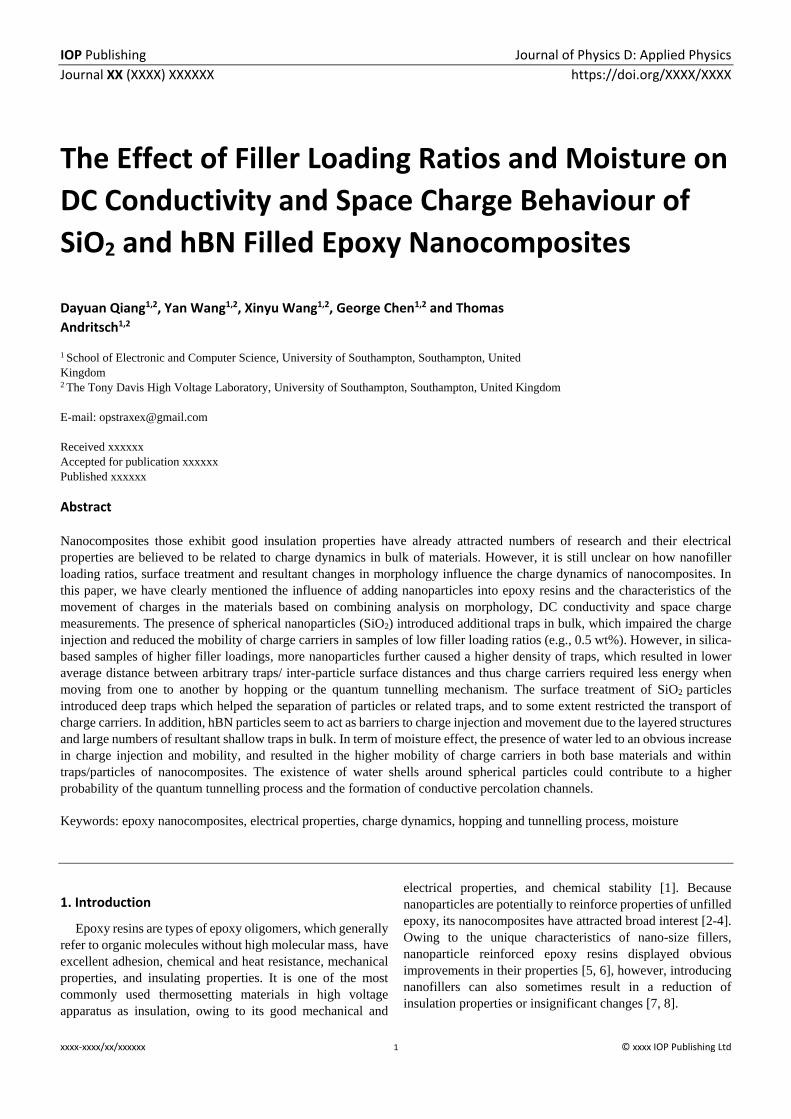
pure specimens are shown in Fig. 15.
Journal XX (XXXX) XXXXXX Dayuan Qiang et al
7
FIG. 15 Space charge profile of pure samples at 40 kV·mm-1, dry.
As the PEA system only measures the net charges, this
might be covered by the charge injection. Thus, in an attempt
to reflect more details of the charge distribution in bulk, a
subtraction method was employed to remove the capacitive
charges from the electrodes [29]. In this method, the reference
data is multiplied by the ratio between the applied voltage and
a reference voltage; this can be considered as the charge
density data at the applied voltage without the effect of space
charges in bulk. The actual measured charge density data
obtained from the volts-on measurement minus the multiplied,
will reveal the injected charges in the sample and its induced
charge at the electrodes. This can be expressed as below [29]:
(1)
where and are the reference and applied voltages,
is the space charge density after subtraction, and
and represent the charge density at the applied
voltage and reference voltage respectively. This method is
applied to the results of unfilled epoxy (shown in Fig. 16) and
all the nanocomposites.
Moreover, the total charge amount and charge density
within the bulk of the sample can be calculated using
Equations 2 and 3, as follows:
(2)
(3)
where and are the charge density of positive
and negative charges respectively, is the electrode area
equal to 50.265 mm2 (with a radius of 4 mm), is the
thickness of samples (145 ± 10 µm), is the total charge
amount, and is total charge density in
bulk.
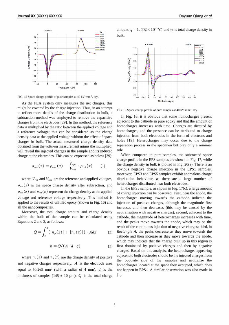
FIG. 16 Space charge profile of pure samples at 40 kV·mm-1, dry.
In Fig. 16, it is obvious that some homocharges present
adjacent to the cathode in pure epoxy and that the amount of
homocharges increases with time. Charges are dictated by
homocharges, and the presence can be attributed to charge
injection from both electrodes in the form of electrons and
holes [19]. Heterocharges may occur due to the charge
separation process in the specimen but play only a minimal
role.
When compared to pure samples, the subtracted space
charge profile in the EPS samples are shown in Fig. 17, while
the charge density in bulk is plotted in Fig. 20(a). There is an
obvious negative charge injection in the EPS1 samples;
moreover, EPS3 and EPS5 samples exhibit anomalous charge
distribution behaviour, as there are a large number of
heterocharges distributed near both electrodes.
In the EPS5 sample, as shown in Fig. 17(c), a large amount
of charge injection can be observed. First, near the anode, the
homocharges moving towards the cathode indicate the
injection of positive charges, although the magnitude first
increases and then decreases (this may be caused by the
neutralisation with negative charges); second, adjacent to the
cathode, the magnitude of heterocharges increases with time,
and the peaks move towards the anode, which may be the
result of the continuous injection of negative charges; third, in
Rectangle A, the peaks decrease as they move towards the
cathode and then increase as they move towards the anode,
which may indicate that the charge built up in this region is
first dominated by positive charges and then by negative
charges. Based on this analysis, the heterocharges appearing
adjacent to both electrodes should be the injected charges from
the opposite side of the samples and neutralise the
homocharges located at the space they occupied, which does
not happen in EPS1. A similar observation was also made in
[1].

Journal XX (XXXX) XXXXXX Dayuan Qiang et al
8
Moreover, since the PEA technique can only show the net
charge distribution in bulk, the total charge amount of EPS3
before 750s is lower than that of and EPS1 (as shown in
Fig. 20(a)), which is due to the neutralisation at both
electrodes. The analysis above suggests that samples filled
with more untreated SiO2 particles will have a larger charge
injection and higher charge mobility in bulk. In other words,
as conductivity is the product of charge carrier concentration
and mobility , they will have higher conductivity. This is
consistent with the results observed in section 3.2.
FIG. 17 Subtracted space charge profile of EPS at 40 kV·mm-1: (a) 1 wt%;
(b) 3 wt%; (c) 5 wt%, dry (dash curves indicate the ideal charge distributions
without neutralisation).
FIG. 18 Subtracted space charge profile of EPST at 40 kV·mm-1: (a) 1 wt%;
(b) 3 wt%; (c) 5 wt%, dry (dash curves indicate the ideal charge distributions
without neutralisation).
The subtracted space charge distribution in the EPST
samples are shown in Fig. 18, while the charge density in bulk
is plotted in Fig. 20(b). In EPST1, homocharges are presented
at both electrodes and move towards the middle of the sample.

Journal XX (XXXX) XXXXXX Dayuan Qiang et al
9
FIG. 19 Subtracted space charge profile of EPB at 40 kV·mm-1: (a) 1 wt%;
(b) 3 wt%; (c) 5 wt%, dry.
Moreover, as shown in Fig. 20(b), the lower charge
injection rate of EPST1 at the beginning may be evidence for
deep traps introduced by the surface treatment presence of
which is proved by our previous work [24] and would restrict
the charge mobility in bulk. Moreover, with the increase of
filler loadings, fast initial charge built-up and similar charge
neutralisation phenomena as in EPS3 and EPS5 are observed
in EPST5. However, the injected charges traveling through the
whole bulk are not as numerous as those in the EPS3 and EPS5
samples, which consequently show heterocharges at both
electrodes.
FIG. 20 Charge density in bulk of pure, EPS, EPST and EPB of 1, 3 and
5 wt%, dry.
Fig. 19 shows the subtracted space charge profile in EPB
samples. Obviously, in EPB samples, charges are dominated
by homocharges. It can be seen that the injected negative
charges gradually increase and move towards the middle of

Journal XX (XXXX) XXXXXX Dayuan Qiang et al
10
the bulk with the growth of filler loading ratios. Moreover,
EPB samples clearly show suppressed injection when
compared to silica-based ones and an increase in initial built-
up charge with the growth of filler loadings, which may refer
to the presence of shallow traps in bulk [13] due to the
morphology in bulk.
FIG. 21 Comparison of space charge decay of charge density in bulk of
epoxy and its nanocomposites of 1, 3 and 5 wt%, dry.
The space decay measurements of pure, EPS, EPST and
EPB samples are then carried out, and the charge densities in
bulk are then summarised in Fig. 21 while space charge decay
rates are calculated and shown in Table 3. Among all types of
samples, the residual charges increase as the filler loading
ratio increases and could indicate more traps in samples due
to the addition of more fillers. EPS samples show a gradually
rising decay rate as loadings increase, which provides
evidence for the existence of traps due to the presence of
nanofillers. However, EPST samples show a contrary trend:
the decay rate decreases, while the residual charge amount in
bulk is the highest among all samples types for each filler
loading. This is caused by the additional deep traps in the
EPST samples, since charges decay slower from deep traps,
which are usually related to chemical changes in bulk, than
from shallow traps, which are caused by the physical defects
[30]. The high rate in EPST3 should be caused by increased
charge mobility due to the growth of filler loadings, and with
the further increase in filled particles, the mobility of charge
carriers is restricted. Thus, it can be concluded that the
presence of nano-SiO2 fillers could mainly lead to physical
changes and resultant shallow traps in bulk, while surface
treatments act as chemical changes that will introduce more
deep traps. Regarding the EPB samples, residual charge
amounts in bulk are the lowest compared to EPS and EPST
(shown in Fig. 21), and the space charge decay rates increase
with the growth of filler loadings, especially in EPB5 (shown
in Table 3). Thus, according to the previous analysis, the traps
in EPB samples are likely to be shallow traps. As mentioned
in the above discussion of the morphology of EPB samples
(see section 3.1), these traps are due to the presence of hBN
particles which result in physical defects [30] such as layered
structures/cracks.
Table 3 Space charge decay rate of epoxy and its nanocomposites.
Sample
Code
Filler Loading Ratio
0 wt% 1 wt% 3 wt% 5 wt%
EP 1.13E+23 - - -
EPS - 1.18E+23 1.36E+23 1.75E+23
EPST - 1.13E+23 1.47E+23 1.09E+23
EPB - 1.41E+23 1.21E+23 2.58E+23
Regarding the moisture effects on space charge behaviour,
the “volts-on” PEA measurement results of epoxy and its
nanocomposites under ambient and 60% relative humidity
conditions are shown in Fig. 22 to 25. In Fig. 22, pure samples
show that the homocharge injection and initial charge build-
up rate significantly increases with moisture. However, the
magnitude near the cathode decreases and shows an increase
at the anode with the growth of the RH condition. It is noted
that more charges are injected into bulk, and that the presence
of moisture results in the injected charge amounts and
mobilities. Moreover, negative charges present in the middle
of samples under both RH conditions and seem to contain
more in bulk of samples under 60RH.
This should first be attributed to the water molecules that
produce ions (OH-, H3O+) and holes coming from the anode
[14, 31]. More water content means that more ionised charges

Journal XX (XXXX) XXXXXX Dayuan Qiang et al
11
will be present in the bulk of samples. Second, as electrons
can travel through inter-chain spaces [32, 33] where water
could locate, negative charges obviously appear in the bulk of
RH conditioned samples and even neutralise some positive
charges at the anode from 600s onwards (see Fig. 22 (b)).
Moreover, there is also a presence of neutralisation near the
cathode at later times, indicating the movement of positive
charges.
FIG. 22 Subtracted space charge profile of pure samples at 40 kV·mm-1: (a)
A.RH; (b) 60RH.
As shown in Fig. 23, for EPS1 and EPS3, the initial
injection rate and neutralisation phenomena become quicker
and more obvious with the growth of RH conditions and filler
loadings, indicating the higher mobility of both positive and
negative charges. Moreover, more obvious increases in the
magnitude of heterocharges near the anode than those adjacent
to the cathode indicate the dominance of negative charges in
the 60RH condition due to the presence of water in the matrix,
which is also found in pure samples and leads to higher
mobility.
In the case of EPST samples, as shown in Fig. 24 (a), the
charge distribution of EPST1 is dominated by homocharges,
which may be caused by more deep traps in bulk due to the
surface treatment. Once more nanofillers are added, EPST
shows obvious charge injection (see Fig. 24(b)). Unlike the
presence of neutralisation in EPS samples, EPST3 under
A.RH conditions is more dominant by positive charges. As
surface treatment introduces additional deep traps, positive
charges can travel along these traps while becoming more
mobile as water uptake increases. However, when RH
conditions rise to 60%, negative charges still show dominance
and positive charges move inside the bulk of material as
shown in Fig. 24(c).
FIG. 23 Subtracted space charge profile of EPS at 40 kV·mm-1: (a) 1 wt%,
A.RH; (b) 3 wt%, A.RH; (c) 3 wt%, 60RH.
Journal XX (XXXX) XXXXXX Dayuan Qiang et al
12
FIG. 24 Subtracted space charge profile of EPST at 40 kV·mm-1: (a) 1 wt%,
A.RH; (b) 3 wt%, A.RH; (c) 3 wt%, 60RH.
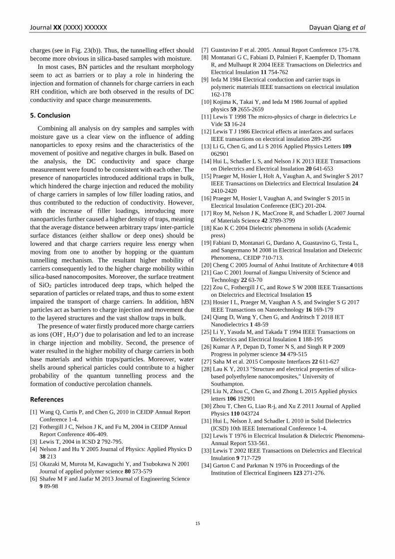
As can be seen in Fig. 25(a) and (b), EPB samples only
show homocharge in bulk, and there is an increase of
magnitude near the cathode as water content rises. Moreover,
there are negative charges in the middle of samples under the
60RH condition. One possible source could be the ions from
water (H3O+ and OH-), while another more important source
is the increased injection in the form of negative charges.
Moreover, when comparing Fig. 25(b) and (c), the
neutralisation in samples with higher filler loadings indicate
the increase in mobility of positive charges, a phenomenon
also found in EPS and EPST samples. This is likely to be due
to the presence of water which contributes to the movement of
positive charges [33].
FIG. 25 Subtracted space charge profile of EPB at 40 kV·mm-1: (a) 1 wt%,
A.RH; (b) 3 wt%, A.RH; (c) 3 wt%, 60RH.
4. Discussion
The term “trap sites” is usually used to explain the charge
dynamics of polymer dielectrics. Regarding conduction in
polymer insulators, taking PE as an example, it is believed to
be dominated by electrons and the transport of carriers takes

Journal XX (XXXX) XXXXXX Dayuan Qiang et al
13
place along the amorphous regions and is limited by traps [34,
35]. One of the mechanisms for charge transport is known as
thermally activated hopping from one trap to another, where
the electron/hole gained sufficient energy could overcome the
potential barrier by thermal fluctuations to reach. Another
mechanism is that an electron/hole can move from one trap to
a close adjacent one by means of quantum mechanical
tunnelling, as an electron is not only well-defined as a particle
and the electron-wave can tunnel through narrow barriers by
simply ‘appearing’ to a nearby trap [36]. Charge mobility is
strongly influenced by the concentration of traps sites and the
presence of nanoparticles could introduce traps around [37].
In case of the hopping process, the relationship between
mobility and concentrations of traps can be expressed by
following equation [38]:
(4)
where is the concentration of traps and is the
localisation length of localised states. It is obvious, in the case
of the hopping process, the mobility of charges is inversely
proportional to the inter-trap distance.
Moreover, in some previous research, tunnelling process is
also suggested to explain charge transport in polymer
nanocomposites with higher filler ratios [13, 39]. There
provides a good way to understand the suppressed charge
transport in samples of low filler loading ratios and increased
charge dynamics in that of high ratios. Equation 5 represents
the characteristic of charge transport by tunnelling mechanism
[39].
(5)
where C and B are constants, is the applied electric field,
is the trap depth or barrier height, is the separation
distance between two adjacent traps in the field direction and
is the characteristic tunnelling distance. Based on this
equation, the charge transport by tunnelling mechanism can be
influenced by three parameters: separation distance between
two adjacent traps, traps depth and the electric field.
Thus, it is easy to understand the charge dynamics in
nanocomposites of 0.5 wt%. For example in Fig. 6, EPS05
shows slightly lower conductivity than pure samples; this is
likely due to the presence of nanoparticles [40], and resultant
traps near the surface could capture the charge carriers (see
Fig. 26(a)). As the inter-traps distance in samples of low filler
ratios is large which is hard for carriers to transport from one
to another, neither by hopping process nor tunelling
mechanism, these trapped charges near the surface generate an
opposite electric field and reduce the applied electric field,
which will hinder the charge injection, thus reducing the
mobility of charge carriers and finally resulting in a reduction
in conductivity [41].
However, with an increase in filler loadings, more
nanofillers will lead to a higher density of traps; this means
the average distance between arbitrary traps should be lower
in samples with higher filler loadings and that charge carriers
will require less energy when moving from one to another (as
shown in Fig. 26 (b)). The resultant increased carrier mobility
will lead to higher conductivity. Moreover, the observed
phenomena of neutralisation in space charge behaviour of EPS
is recombination of positive and negative charges. If regarding
nanofillers as recombination centres [33], the shorter average
surface distance between nanoparticles in samples of high
filler loadings (shown in Table 4) should also result in a higher
conductivity value. EPST samples should share a similar
mechanism and it is easy to understand their lower charge
mobility in bulk.
FIG. 26 Schematic of charge distribution in nanocomposites of uniformly
distributed traps with: (a) low loading ratio; (b) high loading ratio.
EPB samples are slightly different from silica-based
samples. This is likely due to the vastly more complex
morphology in bulk (as has been shown in section 3.1) and the
enormous traps adjacent to the surface, which not only come
from the presence of nanoparticles but also the resultant
morphology of matrix (shown in Fig. 5), significantly reduce
the applied electric field and thus the amount of injected

Journal XX (XXXX) XXXXXX Dayuan Qiang et al
14
charges. Presence of plate-like nano-hBN fillers seem to act as
barriers for charge injection and movement, and lead to lower
conductivity (as shown in Fig. 8) which is determined by the
product of , even in the samples of high filler loading
ratios.
Table 4 Weighted surface distance of EPS and EPST in filler loading ratios
of 1, 3 and 5 wt%
Sample Code
Weighted
Average
Surface
Distance (nm)
Sample Code
Weighted
Average
Surface
Distance (nm)
EPS1 180.43 EPST1 257.35
EPS3 155.27 EPST3 200.08
EPS5 121.59 EPST5 157.97
Table 5 Weighted surface distance of EPS and EPST samples in 1 and 3wt%
under dry, 60RH and saturated conditions
Sample Code Dry (nm) 60RH (nm) Saturated (nm)
EPS1 180.43 157.93 137.09
EPS3 155.27 134.92 115.50
EPST1 257.35 239.58 224.29
EPST3 200.08 178.22 155.31
In term of moisture effect, presence of water in bulk will
surely increase the charge injection and mobility according to
the results of pure samples. In EPS and EPST samples,
increased conductivity is evident in samples of higher filler
loadings. Firstly, this is due to the presence of more water,
leading to higher mobility values of charge carriers in both
base materials and within traps/particles. Secondly, to
consider the effect of the shorter distance between traps due to
presence of particles, the surface distances of EPS and EPST
samples under dry, 60RH and saturated conditions based on
the water-shell model and shell thickness analysis in our
previous work (higher the RH condition, thicker the water
shell) [24] are presented in Table 5. It is obvious that shorter
average surface distance is evident in samples with higher
water content and filler loadings; this will make it easier for
carriers to move from one trap site to another if particles are
regarded as recombination centres [33]. In some cases, the
overlapped water shells could even provide channels for
charge carriers to travel through. This is schematically shown
in Fig. 27. Moreover, the effect of hopping and quantum
tunnelling processes may be more obvious in higher RH
conditions. As hopping distance may be larger than the
distance stated in Table 5, it is assumed that the tunnelling
effect may become much more significant due to the presence
of moisture. Some researchers have reported various
tunnelling distances between traps, and one has quantified it
as ~10 nm [42]. If this value is taken as the threshold of
tunnelling, the percentages of the surface distances between
one particle and the closest one that are smaller than 10 nm
under dry, 60RH and saturated conditions are listed in
Table 6.
FIG. 27 Schematic of charge distribution in nanocomposites of uniformly
distributed traps with water shells.
Table 6 Percentage of weighted surface distance <10 nm of EPS and EPST
samples in 1 and 3wt% under dry, 60RH and saturated conditions
Sample Code Dry (%) 60RH (%) Saturated (%)
EPS1 17.25 48.61 65.57
EPS3 18.50 49.73 70.32
EPST1 14.57 40.13 51.79
EPST3 16.54 48.48 62.88
As shown in Table 6, it is noted that, under the dry
condition, the percentages of both EPS and EPST are lower
than 20% and increase slightly with the growth of filler
loadings. Moreover, the slightly smaller ones in the EPST
samples are likely due to the surface treatment. With the
presence of moisture, the percentages show significant
increases of ~30% in samples under 60RH condition and a
further increase ~10-15% in saturated ones. A similar ratio is
also found in the experimental results of the conductivity of 3
wt% samples, as is shown in Fig. 12 and 13, rather than the
ratio of water uptake between these two RH conditions (in
previous work [24]). Results for 1 wt% show similar trends.
This is also supported by the results of space charge behaviour
in Fig. 23 and 24. The reduction in the distance of arbitrary
deep traps (introduced by surface treament) related to the
inter-particle distance may result in the higher probability of
trapped charges passing through the potential well by the
quantum tunnelling mechanism [13] (based on results of
EPST3 relative to EPST1 in Table 6), which could contributes
to the dominance of positive charges and move-in in EPST3
(see in Fig. 24(b)) while EPS3 is more dominant by negative
Journal XX (XXXX) XXXXXX Dayuan Qiang et al
15
charges (see in Fig. 23(b)). Thus, the tunnelling effect should
become more obvious in silica-based samples with moisture.
In most cases, BN particles and the resultant morphology
seem to act as barriers or to play a role in hindering the
injection and formation of channels for charge carriers in each
RH condition, which are both observed in the results of DC
conductivity and space charge measurements.
5. Conclusion
Combining all analysis on dry samples and samples with
moisture gave us a clear view on the influence of adding
nanoparticles to epoxy resins and the characteristics of the
movement of positive and negative charges in bulk. Based on
the analysis, the DC conductivity and space charge
measurement were found to be consistent with each other. The
presence of nanoparticles introduced additional traps in bulk,
which hindered the charge injection and reduced the mobility
of charge carriers in samples of low filler loading ratios, and
thus contributed to the reduction of conductivity. However,
with the increase of filler loadings, introducing more
nanoparticles further caused a higher density of traps, meaning
that the average distance between arbitrary traps/ inter-particle
surface distances (either shallow or deep ones) should be
lowered and that charge carriers require less energy when
moving from one to another by hopping or the quantum
tunnelling mechanism. The resultant higher mobility of
carriers consequently led to the higher charge mobility within
silica-based nanocomposites. Moreover, the surface treatment
of SiO2 particles introduced deep traps, which helped the
separation of particles or related traps, and thus to some extent
impaired the transport of charge carriers. In addition, hBN
particles act as barriers to charge injection and movement due
to the layered structures and the vast shallow traps in bulk.
The presence of water firstly produced more charge carriers
as ions (OH-, H3O+) due to polarisation and led to an increase
in charge injection and mobility. Second, the presence of
water resulted in the higher mobility of charge carriers in both
base materials and within traps/particles. Moreover, water
shells around spherical particles could contribute to a higher
probability of the quantum tunnelling process and the
formation of conductive percolation channels.
References
[1] Wang Q, Curtis P, and Chen G, 2010 in CEIDP Annual Report
Conference 1-4.
[2] Fothergill J C, Nelson J K, and Fu M, 2004 in CEIDP Annual
Report Conference 406-409.
[3] Lewis T, 2004 in ICSD 2 792-795.
[4] Nelson J and Hu Y 2005 Journal of Physics: Applied Physics D
38 213
[5] Okazaki M, Murota M, Kawaguchi Y, and Tsubokawa N 2001
Journal of applied polymer science 80 573-579
[6] Shafee M F and Jaafar M 2013 Journal of Engineering Science
9 89-98
[7] Guastavino F et al. 2005. Annual Report Conference 175-178.
[8] Montanari G C, Fabiani D, Palmieri F, Kaempfer D, Thomann
R, and Mulhaupt R 2004 IEEE Transactions on Dielectrics and
Electrical Insulation 11 754-762
[9] Ieda M 1984 Electrical conduction and carrier traps in
polymeric materials IEEE transactions on electrical insulation
162-178
[10] Kojima K, Takai Y, and Ieda M 1986 Journal of applied
physics 59 2655-2659
[11] Lewis T 1998 The micro-physics of charge in dielectrics Le
Vide 53 16-24
[12] Lewis T J 1986 Electrical effects at interfaces and surfaces
IEEE transactions on electrical insulation 289-295
[13] Li G, Chen G, and Li S 2016 Applied Physics Letters 109
062901
[14] Hui L, Schadler L S, and Nelson J K 2013 IEEE Transactions
on Dielectrics and Electrical Insulation 20 641-653
[15] Praeger M, Hosier I, Holt A, Vaughan A, and Swingler S 2017
IEEE Transactions on Dielectrics and Electrical Insulation 24
2410-2420
[16] Praeger M, Hosier I, Vaughan A, and Swingler S 2015 in
Electrical Insulation Conference (EIC) 201-204.
[17] Roy M, Nelson J K, MacCrone R, and Schadler L 2007 Journal
of Materials Science 42 3789-3799
[18] Kao K C 2004 Dielectric phenomena in solids (Academic
press)
[19] Fabiani D, Montanari G, Dardano A, Guastavino G, Testa L,
and Sangermano M 2008 in Electrical Insulation and Dielectric
Phenomena,. CEIDP 710-713.
[20] Cheng C 2005 Journal of Anhui Institute of Architecture 4 018
[21] Gao C 2001 Journal of Jiangsu University of Science and
Technology 22 63-70
[22] Zou C, Fothergill J C, and Rowe S W 2008 IEEE Transactions
on Dielectrics and Electrical Insulation 15
[23] Hosier I L, Praeger M, Vaughan A S, and Swingler S G 2017
IEEE Transactions on Nanotechnology 16 169-179
[24] Qiang D, Wang Y, Chen G, and Andritsch T 2018 IET
Nanodielectrics 1 48-59
[25] Li Y, Yasuda M, and Takada T 1994 IEEE Transactions on
Dielectrics and Electrical Insulation 1 188-195
[26] Kumar A P, Depan D, Tomer N S, and Singh R P 2009
Progress in polymer science 34 479-515
[27] Saha M et al. 2015 Composite Interfaces 22 611-627
[28] Lau K Y, 2013 "Structure and electrical properties of silica-
based polyethylene nanocomposites," University of
Southampton.
[29] Liu N, Zhou C, Chen G, and Zhong L 2015 Applied physics
letters 106 192901
[30] Zhou T, Chen G, Liao R-j, and Xu Z 2011 Journal of Applied
Physics 110 043724
[31] Hui L, Nelson J, and Schadler L 2010 in Solid Dielectrics
(ICSD) 10th IEEE International Conference 1-4.
[32] Lewis T 1976 in Electrical Insulation & Dielectric Phenomena-
Annual Report 533-561.
[33] Lewis T 2002 IEEE Transactions on Dielectrics and Electrical
Insulation 9 717-729
[34] Garton C and Parkman N 1976 in Proceedings of the
Institution of Electrical Engineers 123 271-276.

Journal XX (XXXX) XXXXXX Dayuan Qiang et al
16
[35] Pelissou S, St-Onge H, and Wertheimer M 1988 IEEE
transactions on electrical insulation 23 325-333
[36] Merzbacher E 1998 Quantum Mechanics Inc., New York
[37] Takada T, Hayase Y, Tanaka Y, and Okamoto T 2007 Annual
Report-Conference on Electrical Insulation and Dielectric
Phenomena 417-420.
[38] Baranovski S and Rubel O 2006 Description of charge
transport in amorphous semiconductors Charge transport in
disordered solids with applications in electronics 49-96
[39] Chen G, Li S, and Zhong L 2015 in Properties and
Applications of Dielectric Materials (ICPADM) 36-39.
[40] Lau K, Vaughan A, Chen G, Hosier I, Holt A, and Ching K Y
2014 IEEE Transactions on Dielectrics and Electrical Insulation
21 340-351
[41] Chen G, Tay T, Davies A, Tanaka Y, and Takada T 2001 IEEE
Transactions on Dielectrics and Electrical Insulation 8 867-873
[42] Lubyshev D I, González‐Borrero P P, Marega E, Petitprez E,
La Scala N, and Basmaji P 1996 Applied Physics Letters 68
205-207