the game of arkanoid - ernetthe game of arkanoid students: ankit gupta 2003cs10153 ravi gupta...
TRANSCRIPT

DIGITAL HARDWARE DESIGN
PROJECT REPORT
The Game Of Arkanoid
Students: Ankit Gupta 2003CS10153 Ravi Gupta 2003CS10185
Instructor: Prof. M. Balakrishnan

INDEX
1. Functionality of the Project 2. Input Output Block Diagram 3. Design Description 4. Simulation 5. UCF File 6. Implementation Details 7. Refinements 8. Conclusion

FUNCTIONALITY OF THE PROJECT
The objective of the project is to build an arcade game using the Xilinx FPGA kit.
The red player is on the base line. The blue ones are the bombs falling randomly from the top. The purple one represents the bullet shot by the player. The player can move horizontally on the base line and shoot the bombs. He has to avoid collision with the bombs. Once he collides he loses the chance and the game has to be restarted now.

INPUT-OUTPUT BLOCK DIAGRAM
The user interface from the keyboard is: a) 9 : resetting the game b) 7 : starting the game again c) * : move left d) # : move right e) 8 : shoot the bullet The display on the LED matrix is made blank once you lose a life. The game has to be restarted by the pressing 7 “start”.

DESIGN DESCRIPTION
BLOCK DIAGRAM

1. INPUT INTERFACE
Input Interface Inputs: a) 15 Hz clock b) 16K clock Outputs: a) RESET : reset the system b) SHOT : shoot a bullet c) SHR : move player left d) SHL : move player right e) LEVELLER : change the playing level

This subsystem consists of two major parts as seen in the following image: One is the standard keyboard interface. It takes in two clocks and gives out the following signals:
a) keypress b) star c) hash d) 4 bit number
The other part is a decoding system which checks for various keyboard keys as inputs and passes them further for processing. 2. MAIN STATE MACHINE
State Diagram (8MHz)

Input: a) CLK : 8MHz clock b) RESET : resetting the game to start it afresh c) START : for starting the game d) ENDLIFE : signal to indicate if one life is over Output: a) S1 : reinitialize the whole system for new game b) showother : signal for showing nothing on the LEDs 0 => valid display 1 => no display
3. PLAYER
Player module

Inputs: a) CLOCK : 8 MHz clock for the internal state machine
of the top module (explained below ) b) SHR : move the player left (shifting right) c) SHL : move the player right (shifting left) d) LD : repositioning the player for a new game Outputs: a) PL : 3 bit signal for the column in which the left part of the player is b) PC : 3 bit signal for the column in which the center part of the player is c) PR : 3 bit signal for the column in which the right part of the player is Functionality: This subsystem stores the position of the player at any time and reflects the changes done while the player is moved while the course of the game. Implementation: The basic idea is to store the three positions of the player in three data registers. This data can be shifted either to the right or to the left. At any time the next data to be put, for both right and left movement is made available. The shift right signal selects the data to be updated. Thus the implementation is basically of a bi-directional shift register with the basic storage element being a collection of 3 bits. Depending on the shift left or shift right signal, the appropriate data is selected.

NOTE:
0 1 2 3 4 5 6 7 0 1 2 3 4 5 6 7 {2,3,4} goes to {1,2,3} , hence for left movement, the data of player needs to be shifted right. Similarly, for right movement, the data of the player needs to be shifted left. The implementation of this bi-shift register is done by a data part and a state machine. The data part is:

The clock for these registers is generated by the following state machine:
State Machine (8MHz)
This state machine generates the clock for loading the data into the register once the data to be loaded has been made totally stable.
4. BULLET This module stores and regularly updates the position of the bullet on the 8X8 LED matrix. It also takes in the bomb data and regularly checks if at any time the bullet has hit a bomb, that is the position of the bomb and the bullet become equal. It generates the “end signal” on such an event. Also, once the end signal is generated the positions of the hitting bullet are passed on to the “bomb module” which then removes that bomb from its storage.

The implementation off the above module is done in the following way:
The description of the “BULLETS” is given below. The data register is used to store the data of the bullet which has hit the bomb. NOTE: The “BUL” signal changes after a short time but in the mean time the “end” signal coming as the clock stores this value in the register. If this had not been done, then the BUL signal could not have been used for checking which bomb has been actually hit. The implementation in terms of the data part and the state machine is on the following page:

Bullet Storage Module (Data Part) Two four bit counters are used to store the rows and columns of the bullet. The column counter is set to an invalid value of 15 if there is no bullet in the field. The row counter is continuously decremented at a rate of 15 HZ and reset to 7 once it has reached 15. The shoot signal indicates that a new bullet is being shot. The bullet is shot from the center of the player(BOMB_ROW).

NOTE: The control has been set up in such a manner that there can be only one bullet in the field at a time.
Inputs: set, end, shoot
State Machine (8MHz) Inputs: a) set: tells if the row has reached the value of 15 so it is a time to set it to 7 now. b) end: tells if a bullet has hit a bomb. If yes then the bullet must
invalid now. c) shoot: external signal to shoot a new bullet

Output: a) ld: signals the shooting of a new bullet and loads the column at which the bullet was shot in the column register and the row register is reset to 7. 5. BOMBS
Before going to the actual implementation, the representation and storage of bombs is discussed. Note that we can have a maximum of 64 bombs on the 8X8 LED matrix display.
8 8 8 … … … … … live bomb invalid bomb
In this way, in each 8 bit register, we store the status of bombs in each row. This data is shifted at the rate of 1-2 Hz which the rate at which the bombs are being dropped.
The actual implementation consists of using a module which
is store of eight 8 bit registers on which various operations are defined. Each of the eight bit registers has been implemented using 8 D flip flops. This has been done because bit level control is needed to have access to each bomb in the system.

The actual implementation is described on the next page:
Data Part
ROM: This is a 32X8 bits memory which stores the data of which set of bombs to let fall at a time. The data stored in the ROM is:
DEPTH 32 WIDTH 8 RADIX 16 ADDRESS DATA 00: FF, 01: 01, 02: 02, 03: 04, 04: 08, 05: 10, 06: 20, 07: 40, 08: 80, 09: 00,

0A: 01, 0B: 02, 0C: 04, 0D: 08, 0E: 10, 0F: 20, 10: 40, 11: 80, 12: 00, 13: 10, 14: 00, 15: 00, 16: 10, 17: 44, 18: 00, 19: 10, 1A: 50, 1B: 02, 1C: 10, 1D: 01, 1E: 30, 1F: 10 BOMB2: It is the set of eight 8 bit registers described earlier.
It allows the following operations: a) Resetting all the 64 bits to the initial data b) Resetting one bit given its correct position and register
of occurrence. (i.e. making a bomb invalid once it is hit)
c) Shifting the data at 8 bit level. (i.e. letting the bombs fall). Each of these registers represent a row of bombs on the LED matrix.

Functionality: Once the positive clock edge comes, a new set of bombs has to be dropped. So the whole 8 blocks of data is shifted and the new data coming from an address in the ROM is loaded into the 0th row block. The controls for loading the data comes from the following state machine:
State Machine (16K)

Here the BombDrop signal is same as the BCLK signal shown in the data part. This naming has been redone so as to avoid any confusion with the clock of 8MHz with which the state machine works. The edge transition from S2 to S3 ensures that the data from the ROM has been stabilized to be put into the data registers.
Inputs:
a) load : for loading the initial data into the registers b) bomclk : this is clock of about 1 Hz which determines the rate at which the bombs fall. It is generated using the 4 bit counter with 15 Hz clock. Decoding 15 in this counter gives the clock of about 1 Hz. c) end : this signal indicates that a bomb has been hit and its time to invalidate the bomb. d) hitting_bullet : this 7 bit bus gives me the address of the bomb which is hit. Outputs: Zero [7-0] One [7-0] Two [7-0] Three [7-0] Four [7-0] Five [7-0] Six [7-0] Seven [7-0] These are the eight buses which give out the whole data about the status of bombs in the 64 bit system.

6. Display Bombs
DATA PART This module is used to multiplex the data of eight bombs of each row sequentially for display as well as checking with the bullet collision. This output is also used for testing if the player has collided with any of the bombs. The selecting in the MUXes is basically done through 6 bits of a continuously incrementing counter at 16K. The upper three bits are first used to select the row which is to be displayed. This gives me the 8 bits of the row with each bit standing for the life of the bomb at that position. Now the lower 3 bits are used to select the column out of these live bits. Since a counter is being used, the lower 3 bits will traverse the bombs of a row once every time the upper three bits change thus leading to proper display of bombs. Also note that this

sequential data of the bombs is also used for testing their collision with the bullets. The data of the bombs should not change before every bomb has been displayed at least once. So, Let tbomclk be the time period of the clock which controls the falling of the bombs and tbomparse be the rate at which the counter for parsing the display data sequentially is run. tbomclk > 64 * tbomparse
fbomparse > 64 * fbomclk fbomparse > 64 Hz
Hence the clock being used for display is 4 KHz which is perfectly fine. The counter for parsing is a 7 bit counter. The limit of the counter is 67. This is done with the view that the msb is used to multiplex later the data between the bombs(BZ) and the (player+bullet)(AZ). Once it reaches 0 to 63, it shows the data of the bombs and once the msb becomes 1, the player and bullet are displayed and then the cycle restarts again. This explains the logic behind displaying the data using the technique of sequential multiplexing. Now, the rest of the display components will be shown. The logic behind their implementation has been explained above. Also note that depending on the livebomb signal, we multiplex the current value the counter(depicting the address of bomb) and an invalid value(no display of bomb).

Multiplexing player data and bullet into AZ
Total Multiplexing Of AZ and BZ into the final outputs for the FPGA
Note that if the “gameover” signal is high then an invalid data is passed on to the LED interface so that there is no display.

7. Collision Detection Functionality This module checks if at any moment of time the player has been hit by a bomb. If yes, then it generates the “blasted” signal which is then fed back to the main state machine for processing. This feedback processing has already been discussed. Inputs: a) PL : Left part of the player b) PC : Central part of the player c) PR : Right part of the player d) BZ : Sequential bombs data from the previous module Outputs: a) blasted : 1 means player has been hit by the bullet, 0 means otherwise Implementation: This logic is implemented by simply using 3 comparators, one for each part of the player body and the equality comparison being done with BZ. “blasted” signal is generated by ORing the results of the comparators.

8. 8X8 LED Matrix Display
SCHEMATIC DESCRIPTION This module takes input the 4 bit row and 4 bit column and generates the appropriate control signals for the 8X8 LED matrix display on the FPGA. NOTE: Though 3 bits are enough for selecting among 8 rows and columns, 4 bits for each have been used so that the invalid data (nothing to be displayed) can be distinguished with the valid data for display. This grew out of our need to show nothing on the FPGA at some time instants.
Simulation The whole system is quite complex as a whole to simulate since at any instant of time, the bombs are falling down, the bullet moving up and the player potentially moving left or right. The net number of signals for the output is very large: a) 8X64 bits for bombs b) 8 bits for the bullet c) 16 bits for the player Though these have been multiplexed at the end, but showing all the functionality takes just too long and is not feasible to display in a single sheet. Hence the simulation for the whole system has not been done. Due to the above problem, the timing calculations had to be done by us manually because the system consists of various sub modules working independently at their own frequencies. The timing issues in case of display have been discussed in the display module above.
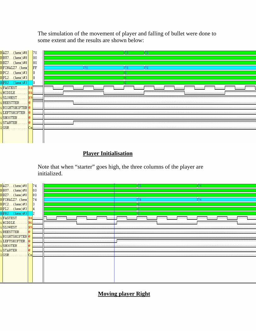
The simulation of the movement of player and falling of bullet were done to some extent and the results are shown below:
Player Initialisation Note that when “starter” goes high, the three columns of the player are initialized.
Moving player Right

Note that as the “left shifter” signal goes high, the player coordinates are moved right.
Shooting a Bullet Note that as shooter goes high, there is a new bullet data in the AZ signal, which is continuously multiplexing the data of player and bullet. We can clearly see the data bullet varying as: 65 55 45 35 25 15 These are some simulations which were done for some particular parts of circuit. As explained above it is not feasible to simulate the circuit as a whole.

Bombs Falling Simulation We can clearly see the data in each row of the matrix (i.e. the bombs falling a regular rate).

UCF FILE # CN 17 TO 20 NET KR0 LOC=P56; NET KR1 LOC=P57; NET KR2 LOC=P58; NET KR3 LOC=P59; NET KC0 LOC=P60; NET KC1 LOC=P61; NET KC2 LOC=P62; # CN 13 TO CN 9 NET C<4> LOC=P14; NET C<5> LOC=P15; NET C<6> LOC=P16; NET C<7> LOC=P17; NET C<0> LOC=P18; NET C<1> LOC=P19; NET C<2> LOC=P20; NET C<3> LOC=P23; NET R<6> LOC=P24; NET R<5> LOC=P25; NET R<2> LOC=P26; NET R<7> LOC=P27; # CN14 TO CN12 NET R<0> LOC=P35; NET G<5> LOC=P36; NET G<4> LOC=P37; NET R<3> LOC=P38; NET R<4> LOC=P39; NET G<0> LOC=P40; NET G<6> LOC=P44; NET R<1> LOC=P45; NET G<7> LOC=P46; NET G<1> LOC=P47; NET G<2> LOC=P48; NET G<3> LOC=P49;

Implementation Results Design Summary: Number of CLBs 271 out of 400 67% Total CLB Flops: 128 out of 800 16% 4 input LUTs: 290 out of 800 36% 3 input LUTs: 105 out of 400 26% 32X1 ROMs: 8 Number of bonded IOBs: 32 out of 61 52% IOB Flops: 0 IOB Latches: 0 Number of pullups: 4 out of 112 3% Number of TBUFs: 72 out of 880 8% Number of OSC: 1 out of 1 100% Total equivalent gate count for design: 4140 Additional JTAG gate count for IOBs: 1536 Device utilization summary: Number of External IOBs 32 out of 160 52% Flops: 0 Latches: 0 Number of OSCILLATORs 1 out of 1 100% Number of PULLUPs 4 out of 112 3% Number of TBUFs 72 out of 880 8% Design statistics: Minimum period: 78.359ns
(Maximum frequency: 12.762MHz) Maximum net delay: 23.303ns

REFINEMENTS The developed system works out quite well in the end. The various refinements which could have been done are: 1. Better Display At this point of time, there is some problem in the display that is a particular set of LEDs glow without any control. We have identified the problem with this. This is because of multiplexing of data at a very high rate. Since the number of elements to be glown at any instant of time is very large, we have no choice but to sequentially multiplex the data into the FPGA. The identified solutions to this problem are: a) Slower clock can be used but that deteriorated the display of other elements as the blinking increases. This is again due to the the large number of elements to be displayed. b) At present, any LED on the field can be a bomb in our system. The number of elements to be displayed can be drastically reduced if we decide to keep only one live bomb in each row. That would reduce the number to only 12 elements to displayed in comparison to 67 now. This can certainly improve the quality if the display. c) The LED matrix module can be redisgned to take the input as we want it to have. That is, if we can have a module that simultaneously taken in a set of positions and glow those LEDs then that can certainly be of a great help. 2. Scoring The score can be displayed on the seven segment LED display on the FPGA. This could not be done because we could not find a single FPGA kit on which the connector 21 would work fully fine. Some boards which we tested did not have enough

working pins so as to possibly connect them with the SSD. The scoring is done internally but cannot be transferred outside. 3. Multi Level Game This can be brought in quite easily by using different ROMs for storage of bombs. With the increasing score, the ROMs can be multiplexed to go to higher level after the player acquires a particular set of score limit. 4. Multiple Life Game At present, the player is given a new life every time. A functionality can be put in such that the new lives do not come once the player has got over with a preset number of lives. This is a trivial change which requires only the main state machine to be changed and nothing else.

CONCLUSION
The objective of the project has been duly fulfilled by developing the above game with the specifications we thought of. It could have been much better with the above mentioned refinements if some more time would have been there. In all, it was a very nice and learning experience in the lab and we heartily thank our instructor Prof. M. Balakrishnan, Teaching Assistant : Anant Vishnoi, and Lab Assistant MrSharma for their due support.