the influence of clamping and residual stress on …
TRANSCRIPT

The Pennsylvania State University
Department of Materials Science and Engineering
THE INFLUENCE OF CLAMPING AND RESIDUAL STRESS ON SCALING EFFECTS
IN Pb(Zr0.3Ti0.7)O3 THIN FILMS FOR PIEZOMEMS APPLICATIONS
A Dissertation in
Your Graduate Major
by
Lyndsey M. Denis
© 2019 Lyndsey M. Denis
Submitted in Partial Fulfillment
of the Requirements
for the Degree of
Doctor of Philosophy
August 2019

ii
The dissertation of Lyndsey M. Denis was reviewed and approved* by the following:
Susan Trolier-McKinstry
Professor of Ceramic Science and Engineering and Electrical Engineering
Dissertation Advisor
Chair of Committee
Clive Randall
Professor of Materials Science and Engineering
Roman Engel-Herbert
Associate Professor of Materials Science and Engineering, Chemistry, and Physics
Michael Lanagan
Professor of Engineering Science and Mechanics
Jacob Jones
Special Member
Professor of Materials Science and Engineering
North Carolina State University
Suzanne Mohney
Professor of Materials Science and Engineering and Electrical Engineering
Chair, Intercollege Graduate Degree Program in Materials Science and Engineering
*Signatures are on file in the Graduate School

iii
Abstract
Ferroelectric thin films such as lead zirconate titanate (PZT) have high dielectric
and piezoelectric properties which can be utilized in actuators, sensors, transducers, and
energy harvesters in microelectromechanical systems (MEMS). A small film thickness
enables low voltage operation of such devices; however, property degradation limits the
extent that the film thickness can be reduced while maintaining performance. This
dissertation describes the impact that different electrical and mechanical boundary
conditions have on the dielectric properties of PZT thin films for a variety of thicknesses
(ranging from 0.27 to 1.11 µm). Specifically, variations in elastic layer thickness,
substrate clamping, residual stress and domain state were investigated. A novel approach
to quantitatively deconstruct the relative permittivity into three contributions (intrinsic,
reversible extrinsic and irreversible extrinsic) was developed using a combination of X-
ray diffraction and Rayleigh analysis. This work aims to determine which factors are
associated with scaling effects in tetragonal {001} textured Pb0.99(Zr0.3Ti0.7)0.98Nb0.02O3
(PZT 30/70) thin films.
It is generally accepted that scaling effects play a key role in the suppression of
ferroelectric responses in thin films (< 1 μm), though the type and extent of this
contribution is still debated. Scaling effects refer to the size-induced degradation of
properties at length scales exceeding those associated with the ferroelectric stability limit.
For a blanket PZT 30/70 film clamped to a Si substrate, the thickness dependence of the
irreversible and reversible Rayleigh coefficients was investigated using Rayleigh
analysis. The irreversible Rayleigh coefficient was found to be thickness dependent. By
iv
partially releasing the films from the substrate, the suppression of extrinsic contributions
to the relative permittivity was alleviated. A greater increase in the irreversible Rayleigh
coefficient was observed for thicker films (1.11 μm) compared to thinner films (0.56 μm
– 0.27 μm). Therefore, substrate clamping contributes to scaling effects. After the films
were partially declamped from the substrate, the irreversible contributions increased up to
23% in Nb-doped films and became more frequency-dependent (by up to 29%).
Defects in a low-dielectric, Mn-doped seed layer also suppressed the extrinsic as
well as the intrinsic contributions to the relative permittivity and contributed to the
observed thickness dependence in the irreversible and reversible Rayleigh coefficients.
The influence of the seed layer on dielectric properties was accounted for using a
capacitor in series model. The suppressed frequency dependence in the clamped films
was attributed to the pinning of irreversible domain walls active at lower frequencies.
Both the seed layer and substrate clamping contributed to the pinning of irreversible
domain walls.
The thickness dependence of intrinsic and extrinsic contributions to the dielectric
properties was elucidated from a combination of X-ray diffraction and Rayleigh analysis.
In situ synchrotron X-ray diffraction was used to understand the influence of residual
stress and substrate clamping on the domain state, ferroelastic domain reorientation and
electric-field-induced strain in PZT 30/70 thin films. A thickness-dependent in-plane
tensile stress developed in clamped, blanket PZT films during processing which dictates
the domain structure even after poling. Defects and thermal stresses contribute to the
greater in-plane tensile stress in the thinner films, resulting in this thickness dependence.

v
However, after the films were partially declamped from the substrate and annealed, the
residual stress was alleviated. As a result, the thickness dependence of the volume
fraction of c-domains largely disappeared, and the out-of-plane d-spacings for both a and
c-domains increased in the thinnest film.
By poling the films, irreversible changes in the domain state and domain structure
were induced as a result of 90° domain reorientation, domain coarsening, and lattice
strain. Upon poling, thicker films experienced a greater coarsening of c-domains which
resulted in reduced domain wall densities and a larger change in the reversible Rayleigh
coefficient. The volume fraction of c-domains was used to calculate the intrinsic relative
permittivity; the reversible Rayleigh coefficient was then used to separate the intrinsic
and the reversible extrinsic contributions. The reversible extrinsic response contributed to
more than 70% of the overall relative permittivity and was thickness dependent even after
poling and upon release.
Some PiezoMEMS devices, such as cantilevers and fixed-fixed beams, operate in
a partially released state. For these devices, the thickness of the passive layer is known to
tune the rigidity, deflection and resonance frequency for tailored device performance.
However, as the rigidity of the device increases, at some point the ferroelastic response of
the active layer will be suppressed. Therefore, the influence of passive layer thickness on
the performance of the active layer is of interest.
The deflection of cantilevers and fixed-fixed beams with a tetragonal {001} PZT
30/70 active layer and a SiO2 elastic layer in an IrO2/PZT/PbTiO3/Pt/TiO2/SiO2 device
stack was characterized experimentally and by finite element modeling. Differences in

vi
the magnitude of the tip displacement were attributed to the variances in rigidity of the
device stack associated with different SiO2 thicknesses. It was found that bending of the
cantilevers was dictated by the competing integrated stresses of the IrO2 top electrode and
the SiO2 elastic layer. Upon release, the PZT films showed increased reversible Rayleigh
coefficients but decreased irreversible Rayleigh coefficients, regardless of SiO2 thickness
(2.035 and 0.76 µm), for both cantilever and fixed-fixed beam geometries. These data
suggest that upon release, at least some of the domain walls transition from irreversible to
reversible motion. For cantilevers and fixed-fixed beams with the thinner SiO2 layers, the
electroded PZT region deflected downward, placing PZT under further in-plane tension.
This was correlated with a further decrease in the irreversible and reversible domain wall
motion contributions to the relative permittivity.

vii
TABLE OF CONTENTS
List of Figures ................................................................................................................................. x
List of Tables ............................................................................................................................... xvi
Acknowledgements .................................................................................................................... xvii
Chapter: 1 Introduction and Background ................................................................................... 1
1.1 Piezoelectrics ................................................................................................................. 1
1.2 Ferroelectrics ................................................................................................................. 2
1.3 Lead Zirconate Titanate ................................................................................................. 4
1.4 Ferroelectric Domain Structure and Formation ............................................................. 5
1.5 Rayleigh Analysis .......................................................................................................... 7
1.6 X-ray Diffraction ........................................................................................................... 9
1.7 Residual Stresses in Thin Films ................................................................................... 12
1.8 Scaling Effects ............................................................................................................. 13
Chapter: 2 Thickness Dependent Response of Domain Wall Motion in Declamped {001}
Pb(Zr0.3Ti0.7)O3 Thin Films ............................................................................................ 17
2.1 Introduction ................................................................................................................. 17
2.2 Experimental Procedure............................................................................................... 20
2.2.1 Film Synthesis and Nanofabrication ...................................................................... 20
2.2.2 Characterization ...................................................................................................... 25
2.2.3 Capacitor in Series Model ...................................................................................... 27
2.3 Results ......................................................................................................................... 29
2.3.1 Thickness Dependence of Polarization Hysteresis in Declamped Films ................ 29
2.3.2 Irreversible Contributions to Permittivity .............................................................. 31
2.3.2.1 Thickness Dependence in Clamped Films ..................................................... 31
2.3.2.2 Thickness Dependence in Released Films ..................................................... 33
2.3.3 Frequency Dependence of αε .................................................................................. 35
2.3.4 Intrinsic and Reversible Contributions to Permittivity ........................................... 36
2.3.4.1 Thickness Dependence in Clamped Films ..................................................... 36
2.3.4.2 Thickness Dependence of Released Films ..................................................... 37
2.3.5 Frequency Dependence of εinitial ............................................................................. 38
2.4 Discussion .................................................................................................................... 40

viii
2.4.1 Capacitor-in-Series Model...................................................................................... 40
2.4.2 Substrate Clamping Effects .................................................................................... 42
2.5 Conclusions ................................................................................................................. 43
Chapter: 3 Residual Stress and Ferroelastic Domain Reorientation in Declamped {001}
Pb(Zr0.3Ti0.7)O3 Films ...................................................................................................... 44
3.1 Introduction ................................................................................................................. 44
3.2 Experimental Procedure............................................................................................... 47
3.2.1 Film Synthesis and Nanofabrication ...................................................................... 47
3.2.2 X-ray Measurements and Analysis ......................................................................... 49
3.3 Results and Discussion ................................................................................................ 53
3.3.1 Thickness Dependence of the Domain State .......................................................... 53
3.3.2 Thickness Dependence of Residual Stress ............................................................. 57
3.3.3 Rayleigh poling study ............................................................................................. 67
3.4 Conclusions ................................................................................................................. 73
Chapter: 4 Influence of Elastic Layer Thickness on Mechanical and Ferroelastic Behavior
of PiezoMEMS Beams .................................................................................................... 75
4.1 Introduction ................................................................................................................. 75
4.2 Fabrication ................................................................................................................... 79
4.3 Modeling ...................................................................................................................... 82
4.4 Characterization ........................................................................................................... 83
4.5 Results and Discussion ................................................................................................ 84
4.5.1 Influence of Stress and Thickness on Cantilever Tip Deflection ........................... 84
4.5.2 FEA Modeling of Cantilever Tip Deflection .......................................................... 87
4.5.3 Influence of Etch Process on Fixed-Fixed Beam Buckling .................................... 92
4.5.4 Impact of Nanofabrication and Tip Deflection on Electrical Properties ................ 95
4.6 Conclusions ............................................................................................................... 100
Chapter: 5 Conclusions ............................................................................................................. 102
Chapter: 6 Future Work ........................................................................................................... 107
6.1 Depth Profiling using X-ray Diffraction .................................................................... 107
6.1.1 Glancing-incidence X-ray Diffraction .................................................................. 107
6.1.2 X-ray Nanodiffraction .......................................................................................... 111
6.1.3 In Situ X-ray Microscopy ..................................................................................... 113
6.2 Application of Relative Permittivity Deconstruction ................................................ 115
ix
6.2.1 Assessing the Possibility of a Critical Film Thickness ......................................... 115
6.2.2 Permittivity Deconstruction for Various Compositions ....................................... 116
6.3 TEM Analysis of Domain Structure .......................................................................... 117
6.4 Detecting Dead-layers using Curie-Weiss Behavior ................................................. 117
References ................................................................................................................................... 119
Appendix ..................................................................................................................................... 145
Matlab Codes for Data Processing ......................................................................................... 145
A.1. Capacitor in Series Seed Layer Correction ................................................................ 145
A.2. Rayleigh Analysis for Large Frequency Sweeps ....................................................... 148
A.3. File Conversion to Matlab Files from .diel ................................................................ 150

x
List of Figures
Figure 1-1: A comparison of the cubic paralelectric phase and tetragonal ferroelectric
phase of the perovskite crystal structure ABO3. The displacement is exaggerated for
clarity. .............................................................................................................................. 3
Figure 1-2: The PbTiO3-PbZrO3 binary sub-solidus phase diagram with an overlay
comparison of the dielectric constant (K) vs. mole % of PbTiO3 measured at room
temperature, adapted from B. Jaffe et al.[15] A maximum in K is observed near the
morphotropic phase boundary. The monoclinic phase is not shown. .............................. 5
Figure 1-3: The intrinsic and extrinsic response to an applied electric field. The intrinsic
response is associated with the displacement of the central cation parallel to the
applied field, resulting in the distortion of the unit cell. The extrinsic response is the
movement of interfaces such as 90° and 180° domain walls in a tetragonal system. ...... 6
Figure 1-4: Polarization vs. electric field (P-E) hysteresis loop of a polycrystalline and
single crystal ferroelectric ceramic. The polycrystalline P-E loop was measured on a
{001}-textured, 1.11 µm tetragonal Pb(Zr0.3Ti0.7)O3 thin film. Schematics A-F
represent different domain states during a P-E cycle for an appropriately oriented
single crystal with only 180° domain walls present. ........................................................ 7
Figure 1-5: A diagram of reversible motion of a domain wall within a deep potential
energy well and irreversible motion of a domain wall within a shallow potential
energy well within a potential energy landscape of a ferroelectric material. ................... 9
Figure 1-6: (a) An XRD pattern showing the change in the 002 and 200 peak position
during application of an electric field for a {001}-textured, 1.11 µm tetragonal
Pb(Zr0.3Ti0.7)O3 thin film. (b) A complimentary schematic showing the change in the
out-of-plane d-spacings of a and c-domains during application of electric field in the
out-of-plane direction with crystallographic representations of the d-spacings with
respect to the spontaneous polarization direction (c). The dashed lines in (b)
correspond to the original shape. The red dashed lines in (c) correspond to the
original shape. .................................................................................................................. 10
Figure 1-7: The thickness dependence of the relative permittivity (εr,33) and piezoelectric
coefficient (d33) measured at room temperature of a variety of ferroelectric materials
including polycrystalline and epitaxial PZT thin films with either morphotropic or
tetragonal composition, polycrystalline PLaZT of various compositions, and other
PZT-based and lead-free materials for a variety of processing conditions. Figure
taken from Ihlefeld et al.[34] ........................................................................................... 14
Figure 1-8: (a) A diagram of the low dielectric permittivity regions (light blue) along the
film-substrate interface, film surface and grain boundaries within a thin film with
columnar grains. As the film thickness or grain size is scaled down, the volume
fraction of the low dielectric permittivity regions increases. (b) and (c) shows the
thickness dependence of the relative permittivity (εr) as a result of the scaling of film
thickness and grain size, respectively. This figure is adapted from Ihlefeld et al.[34] .... 15

xi
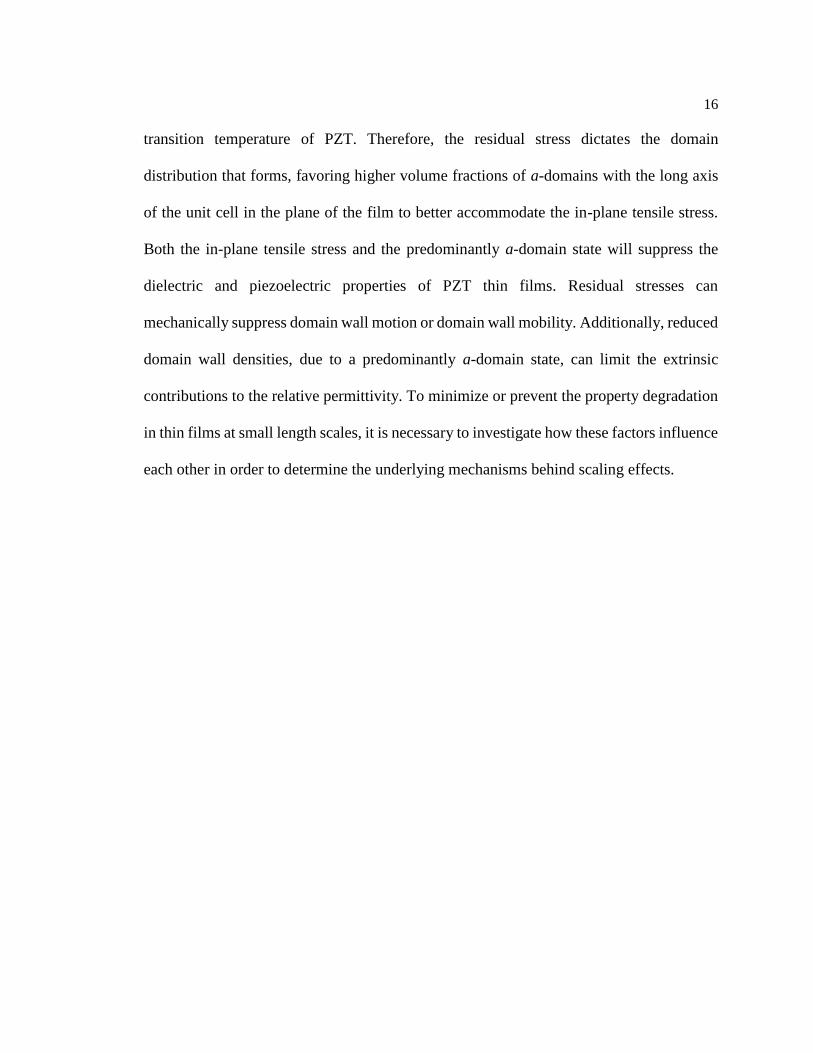
Figure 2-1: X-ray diffraction patterns depicting the dependence of the preferred
orientation of the 1% Mn-doped PZT 30/70 Mitsubishi Materials seed layer on the
spin rates for chemical solution deposition. ..................................................................... 21
Figure 2-2: Schematic of the layer-by-layer crystallization steps used to grow PZT 30/70
thin films ranging in thickness from 0.27 μm to 1.1 μm for (a) films doped with 2%
Nb and (b) films doped with 1% Mn. The cross section of the
Pt/PZT/Pt/TiO2/SiO2/Si stack is also shown. ................................................................... 22
Figure 2-3: Top-down micrographs of PZT 30/70 thin films for thickness ranging from
0.27 μm to 1.1 μm showing the distribution of grain sizes. A cross-sectional
micrograph of the 0.56 μm PZT thin film on a Pt electrode illustrating columnar
grain growth of the film. There is no evidence of porosity or secondary phases. ............ 22
Figure 2-4: (a) A top down view of the Pt electrode for each release state: clamped or
0% released, 25% released, 50% released and 75% released. The different degrees of
release were achieved by varying the density of the etch pits within one electroded
region. (b) 3-D cross-sectional schematics of the release structures including the etch
pits that run vertically through the Pt/PZT/Pt/TiO2/SiO2 stack and the 100 μm
diameter etch trench that was undercut into the Si substrate below each etch pit
region (not to scale). (c) An optical microscope image of the top down view of part
of a released electrode and (d) a cross-sectional micrograph of the released
Pt/PZT/Pt/TiO2/SiO2 stack suspended above the etch trench. ......................................... 24
Figure 2-5: Phase pure X-ray diffraction patterns of tetragonal {001} textured PZT 30/70
thin films doped with 2% Nb and thicknesses ranging from 0.27 μm to 1.1 μm (a, b).
The peak fitting of the 002/200 peaks for the 1.1 μm film is shown (c). The
normalized volume fraction of c-domains (ν002) is also shown as a function of film
thickness (d). Note: error bars are smaller than the symbol size. ..................................... 26
Figure 2-6: (a) Measured relative permittivity vs. a.c. field and (b) frequency dispersion
of the Rayleigh parameter αε and εinitial for clamped the seed layer of 0.06 μm
thickness and 1% Mn-doped PZT 30/70 composition. The frequency dispersion of
the Rayleigh parameter αε (c) and εinitial (d) for clamped 0.38-0.35 μm 1% Mn-doped
PZT 30/70 films grown using PSU-made sol gel compared to a clamped 0.35 μm 1%
Mn-doped PZT 30/70 film grown using Mitsubishi Materials solution is also shown.
The Mitsubishi Materials solution was exclusively used for growth of the 0.06 μm
seed layer.......................................................................................................................... 28
Figure 2-7: Polarization vs. electric field hysteresis loops of clamped 2% Nb-doped PZT
30/70 thin films of varying thickness ranging from 0.27 μm to 1.1 μm. ......................... 30
Figure 2-8: The change in P–E hysteresis loops of 2% Nb-doped PZT 30/70 thin films
between the clamped and 75% released states for (a) 1.11 μm, (b) 0.38 μm, and (c)
0.27 μm thick films. The evolution of the P–E loop for the 0.38 μm thick film is also
shown for clamped, 25%, 50% and 75% released states. ................................................ 31
Figure 2-9: Frequency dispersion of the Rayleigh parameter αε as a function of film
thickness ranging from 0.27 μm to 1.1 μm for PZT 30/70 thin films doped with 2%

xii
Nb in the clamped state before applying the capacitor in series model (Seed + Film)
(a), in the clamped state after applying the model (Film) (b) and in the 75% released
state after applying the model (c). .................................................................................... 32
Figure 2-10: A micrograph of the torn electroded regions extending from the etch pit
after global released. ........................................................................................................ 34
Figure 2-11: Frequency dispersion of the Rayleigh parameter αε as a function of release
state including clamped or 0% released, 25% released, 50% released and 75%
released from the substrate for 0.27 μm thick PZT 30/70 thin film doped with 2%
Nb. .................................................................................................................................... 35
Figure 2-12: Frequency dependence (B) of the Rayleigh parameter αε as a function of
film thickness for PZT 30/70 thin films doped with 2% Nb (a) for the clamped state
before applying the capacitor in series model (Seed + Film), the clamped state after
applying the model (Film), and the 75% release state after applying the model. The
dashed and dotted boxes represent values of B(αε) for the 0.27 and 0.56 μm films,
respectively. Complementary frequency dispersion of the Rayleigh parameter αε are
also shown for thickness 0.27 μm (b) and 0.56 μm (c). ................................................... 35
Figure 2-13: Frequency dispersion of the Rayleigh parameter εinitial as a function of film
thickness ranging from 0.27 μm to 1.1 μm for PZT 30/70 thin films doped with 2%
Nb in the clamped state before applying the capacitor in series model (Seed + Film)
(a), in the clamped state after applying the model (Film) (b) and in the 75% released
state after applying the model (c). .................................................................................... 37
Figure 2-14: Frequency dispersion of the Rayleigh parameter εinitial as a function of
release state including clamped or 0% released, 25% released, 50% released and
75% released from the substrate for 0.27 μm thick PZT 30/70 thin film doped with
2% Nb. ............................................................................................................................. 38
Figure 2-15: Frequency dependence (B) of the Rayleigh parameter εinitial as a function of
film thickness for PZT 30/70 thin films doped with 2% Nb for the clamped state
before applying the capacitor in series model (Seed + Film), the clamped state after
applying the model (Film) and the 75% release state after applying the model. ............. 39
Figure 2-16: The change in the Rayleigh parameters αε (a-b) and εinitial (c-d) as a function
of film thickness for PZT 30/70 thin films doped with 2% Nb. (a, c) Represents the
change after applying the capacitor in series model. (b, d) Represents the change
upon release...................................................................................................................... 41
Figure 3-1: (a) A schematic of the applied electric field cycles during the in situ XRD
study, (b) 2D diffraction image of the PZT 30/70 thin film with labeled reflections,
(c) an example of the changes in peak intensity during application of electric field
for the 1.11 μm PZT film, and (d) Asymmetric Pearson VII fits of the 002 and 200
reflections of the 1.11 μm PZT film at 0*Ec. ................................................................... 50
Figure 3-2: (a) The volume fraction of c-domains (ν002) as a function of applied electric
field is shown for 2% Nb-doped PZT 30/70 thin films of thicknesses 0.27 µm, 0.56
xiii
µm, and 1.11 µm in the clamped state and in the released state. The 75% released
1.11 µm thick film exceeded a threshold current of 1x10⁻⁴ Amps/cm2 at electric
fields exceeding 2*Ec. Therefore, the data for the released 1.11 µm film above
1.5*Ec were removed. (b) The fraction of 90° domain reorientation (η002) as a
function of applied electric field is also shown for the clamped state and the released
state. ................................................................................................................................. 54
Figure 3-3: The evolution of the normalized volume fraction of c-domains (ν001) during
layer-by-layer crystallization for 2% Nb-doped PZT 30/70 thin films processed via
chemical solution deposition for thicknesses ranging from ~80 nm (1 layer) to ~500
nm (6 layers). ................................................................................................................... 55
Figure 3-4: The d-spacing for the 002 (a) and 200 reflections (b) (d002 and d200,
respectively) as a function of applied electric field increment for 2% Nb-doped PZT
30/70 thin films of thicknesses 0.27 µm, 0.38 µm, 0.56 µm, and 1.11 µm in the
clamped state and the 75% released state are shown. ...................................................... 58
Figure 3-5: The thickness dependence of d-spacing for the 200 reflection (d200) for 2%
Nb-doped PZT 30/70 thin films of thicknesses 0.27 µm, 0.56 µm, and 1.11 µm at
room temperature (30 °C) and above the tetragonal to cubic phase transition
temperature (500 °C). ....................................................................................................... 59
Figure 3-6: The d-spacing for the 002 and 200 reflections (d002 and d200, respectively) as
a function of applied electric field increment for 2% Nb-doped PZT 30/70 thin films
of thicknesses (a,e) 0.27 µm, (b,f) 0.38 µm, (c,g) 0.56 µm, and (d,h) 1.11 µm in the
clamped state and the 75% released state are shown and compared to d-spacing
values for their bulk counterparts. .................................................................................... 62
Figure 3-7: (a) The full width half maximum (FWHM) for the 002 and 200 reflections as
a function of applied electric field is plotted for 2% Nb-doped PZT 30/70 thin films
of thicknesses 1.11 µm. (b) FWHM for the 200 reflection as a function of applied
electric field is plotted for clamped films of thicknesses ranging from 0.27 µm to
1.11 µm (left); and FWHM for the 200 reflection as a function of applied electric
field is plotted for the 0.27 µm film for all release states (right). .................................... 63
Figure 3-8: A model of the domain structure within one grain before (left) and after
(right) poling to 3*Ec. In general, the volume fraction of c-domains increases, and
the c-domains coarsen upon application of electric field. ................................................ 64
Figure 3-9: The crystallite size and microstrain as a function of film thickness for 2%
Nb-doped PZT 30/70 thin films in the clamped, unpoled state. ...................................... 65
Figure 3-10: Frequency dispersion of the Rayleigh parameter αε as a function of film
thickness ranging from 0.27 µm to 1.11 µm for 2% Nb-doped PZT 30/70 thin films
in the clamped state for unpoled (a) and poled (b) films, as well as in the 75%
released state for unpoled (c) and poled (d) films. ........................................................... 68
Figure 3-11: Frequency dispersion of the Rayleigh parameter εinitial as a function of film
thickness ranging from 0.27 µm to 1.11 µm for 2% Nb-doped PZT 30/70 thin films

xiv
in the clamped state for unpoled (a) and poled (b) films, as well as in the 75%
released state for unpoled (c) and poled (d) films. .......................................................... 70
Figure 3-12: The intrinsic (εr,intrinsic) and reversible, extrinsic (εr,extrinsic) contributions to
the permittivity as a function of film thickness ranging from 0.27 µm to 1.11 µm for
2% Nb-doped PZT 30/70 thin films in the clamped and 75% released state for
unpoled (a), as well as in the clamped state for unpoled and poled films (b). ................. 71
Figure 3-13: The intrinsic (εr,intrinsic), reversible and irreversible extrinsic (εr,extrinsic)
contributions to the permittivity as a function of film thickness ranging from 0.27
µm to 1.11 µm for 2% Nb-doped PZT 30/70 thin films in the clamped state for
unpoled (a) and poled films (b), as well as in the 75% released state for unpoled (c)
and poled films (d). .......................................................................................................... 73
Figure 4-1: A schematic illustrating the dimensions and film stack of the fixed-fixed
beams, including a top down view of the patterned features (a) and side view of the
device stack (b) with a SEM image of the device with a 2.035 µm SiO2 elastic layer.
Also shown is a schematic listing of the dimensions and film stack for cantilevers of
lengths ranging from 250 µm to 50 µm, including a top down view of the patterned
features (c) and side view of the device stack (d) with a SEM image of cantilevers
with a 2.035 µm SiO2 elastic layer. .................................................................................. 80
Figure 4-2: Vertical displacement of a cantilever across the length (x-position) of a 250
µm long beam for a device with a 2.035 µm thick SiO2 elastic layer and a 0.76 µm
thick SiO2 elastic layer. The cantilever displacements were determined using the
optical profilometry images inset in the graph for each device. ...................................... 85
Figure 4-3: A cross-sectional schematic of the thermal residual stress that develops post-
processing for a multilayered device, with a 0.76 µm thick SiO2 layer and a 2.035
µm thick SiO2 layer, processed on a Si substrate. The z-position of the neutral axis is
shown for each device. ..................................................................................................... 86
Figure 4-4: The mesh used for FEA simulations of the multilayered PiezoMEMS device. ... 88
Figure 4-5: A 2-D COMSOL model of the tip deflection of a 250 µm long cantilever,
and a schematic cross-section showing the residual stress in each layer after
deflection for a device with a 2.035 µm thick SiO2 elastic layer and a 0.76 µm thick
SiO2 elastic layer. ............................................................................................................. 89
Figure 4-6: (a) The linear relationship between the residual stress ratio (σPZT/σSiO2) and
the PZT Young’s Modulus (EPZT) plotted for a device with a 2.035 µm thick SiO2
elastic layer and a 0.76 µm thick SiO2 elastic layer. The comparison is shown for
two different SiO2 Young’s Modulus (ESiO2): 60 GPa and 100 GPa. Contour plots of
σPZT vs. σSiO2 for a variety of cantilever tip displacements for a device with a 2.035
µm thick SiO2 elastic layer (b, d) and a 0.76 µm thick SiO2 elastic layer (c, e) for
𝜎𝐼𝑟𝑂2 for 900 MPa and 1100 MPa.................................................................................. 90
Figure 4-7: The vertical deflection of fixed-fixed beams across the length (x-position) of
a ~1,000 µm long beam for a device with a 2.035 µm thick SiO2 elastic layer and a

xv
0.76 µm thick SiO2 elastic layer. The buckling and vertical deflection of the fixed-
fixed beams were determined using the optical profilometry images inset in the
graph for each device. ...................................................................................................... 93
Figure 4-8: A cross-sectional schematic of the neutral axis and bending moment (M) is
shown across the length of a fixed-fixed beam with a 0.76 µm thick SiO2 layer and a
2.035 µm thick SiO2 layer. ............................................................................................... 95
Figure 4-9: Optical profilometry image of a fixed-fixed beam device with a 2.035 µm
SiO2 layer that is partially and non-uniformly released after an interrupted XeF2
etch. .................................................................................................................................. 95
Figure 4-10: Polarization vs. electric field (P-E) hysteresis loops of an unpoled (a)
clamped PZT 30/70 thin film, (b) cantilever and (c) fixed-fixed beam for a device
with a 2.035 µm thick SiO2 elastic layer and a 0.76 µm thick SiO2 elastic layer. P-E
loops of a poled fixed-fixed beam for devices with the different SiO2 elastic layer
thicknesses are also shown (d). Complementary optical profilometry images are
shown for each device. ..................................................................................................... 96
Figure 4-11: Frequency dispersion of the Rayleigh parameter αε of a (a) clamped PZT
30/70 thin film, (b) cantilever and (c) fixed-fixed beam for a device with a 2.035 µm
thick SiO2 elastic layer and a 0.76 µm thick SiO2 elastic layer. Also included is the
frequency dispersion of the Rayleigh parameter εinitial of a (d) clamped PZT 30/70
thin film, (e) cantilever and (f) fixed-fixed beam for a device with a 2.035 µm thick
SiO2 elastic layer and a 0.76 µm thick SiO2 elastic layer................................................. 99
Figure 6-1: Grazing incidence XRD patterns of polycrystalline PZT 35/65 thin films.
The evolution of the phase coexistence of tetragonal and rhombohedral phases as a
function of incidence angle (i.e. film depth) is shown. This figure was taken from M.
B. Kelman et al.[143] ....................................................................................................... 110
Figure 6-2: Schematics comparing techniques for using nanoprobe X-ray diffraction in
(a) transmission mode and (b) grazing incidence angle reflectance mode in order to
achieve depth profiling of strain and domain distributions in a multilayered
ferroelectric thin film. ...................................................................................................... 112
Figure 6-3: A diagram of the experimental set up for multi-scale 3D imaging of strain
and structure using dark-field X-ray microscopy. Figure taken from H. Simons et
al.[157] ............................................................................................................................. 114

xvi
List of Tables
Table 2-1: Etch conditions for released structures .................................................................. 23
Table 2-2: Frequency dependence of Rayleigh parameter αε (cm/kV) ................................... 39
Table 2-3: Frequency dependence of Rayleigh parameter εinitial ............................................. 39
Table 3-1: Microstructure and Electrical Properties for Clamped PZT 30/70 Films .............. 48
Table 4-1: Film Thickness and Material Properties of Device Layers ................................... 82

xvii
Acknowledgements
I would like to extend my most sincere gratitude to my advisor Professor Susan
Trolier-McKinstry for the mentorship and guidance that she provided during my PhD
studies. Throughout my time at Penn State, I’ve grown intellectually and in self-sufficiency
as a researcher. This is due largely to the hands-on instruction and motivation that Dr.
McKinstry provided, while still giving me the freedom to gain my own experiences and
connections. I am very appreciative of the high expectations she holds for her students
which pushed me to improve myself every day. In particular, I’m most thankful for the
opportunity to learn and adopt her exemplary techniques for effective teaching, a passion
that we both share. Hopefully, in the future, I will have the opportunity to implement this
teaching style in my own classroom.
A special thank you to my undergraduate advisor Professor Jacob Jones who has
continuously invested in my success over the last 10 years, even remotely as my
collaborator at NCSU. As a freshman undergraduate student, I was eager to gain knowledge
in materials science and hands-on experience working in a laboratory. Thankfully, he saw
my potential, valued my assertiveness and offered me an undergraduate research position
in his lab. From this time onward, my love for ceramic processing and my appreciation for
the complexity of ferroelectric materials grew, ultimately fueling my desire to obtain my
Ph.D. in this field.
Over the last 5 years, I have had the privilege of conducting multiple experiments
at national laboratories such as Argonne National Laboratory in Chicago and the European

xviii
Synchrotron Radiation Facility in Grenoble, France. The success of these experiments
would not have been possible without the beamline scientists and beamtime members. In
particular, I would like to thank Yang Ren, Olaf Borkiewicz, Guy Jennings, Rick Spence,
Phil Ryan, and Dmitry Chernyshov for their time during the set up and implementation of
the experiments. They also provided invaluable understanding of ferroelectrics, intellectual
conversation and suggestions for data interpretation. Additionally, I would like to thank
the individual members of the team, which most often included Giovanni Esteves, Hanhan
Zhou, and Julian Walker, among others. The long hours in the car, at the synchrotron
facilities and during night shifts were made exponentially better by the light-hearted nature,
great sense of humor, and unwavering commitment of these friends and colleagues.
I am very grateful for the opportunity to work with colleagues at the Army Research
Laboratory, such as Ron Polcawich, Ryan Rudy, and Jeffrey Pulskamp. Additionally, I
would like to thank Brian Power and Joel Martin of the Army Research Laboratory and
Steven Isaacson of General Technical Services for their assistance in the nanofabrication
of the PiezoMEMS devices used in Chapter 4 of this thesis. The experience that I’ve gained
through this project have helped pave the way towards the start of my career as a research
scientist in a DoD lab.
I would also like to thank past and present STM group members. I was very
fortunate to have senior group members who voluntarily provided equipment training,
processing advice, wisdom, scientific ideas and constructive criticism throughout my Ph.D.
In particular, I would like to thank Trent Borman, Kathleen Coleman, Nicole Hall, Chris

xix
Cheng, Tianning Liu and Dixiong Wang for their shared ideas, conference companionship
and continued friendship.
The research conducted during my Ph.D. would not have been possible without the
training and guidance provided by the Nanofabrication and MCL staff. I wanted to
particularly thank Nichole Wonderling for the many hours she spent with me in the XRD
room calibrating an instrument, analyzing data, perfecting sample alignment, and
designing new and fun attachments for the XRD tools. I also want to thank Beth Jones,
Mike Labella and Bill Drawl for all their help with sample fabrication, sputtering and
photolithography. I have been truly blessed to work in such a friendly and family-like
environment created through the kindness and generosity of the MCL and Nanofab staff.
Thank you to my thesis committee, Professor Clive Randall, Dr. Roman Engel-
Herbert, Professor Michael Lanagan, and Professor Jacob Jones who have supported and
challenged me throughout my Ph.D. They have had uncompromising, high expectations
for the quality of my thesis, education and research, which has led to my exponential
growth as a scientist. For this, I am grateful.
Although my family does not hold degrees in the STEM field and may not
understand the details of my dissertation, they have whole-heartedly supported me through
my graduate studies. I am so incredibly blessed to have their constant love and praise. I
know that, no matter which path I take from here on, they will be nothing but proud.
Through my time at Penn State, I have made lasting friendships with so many
people. I would like to thank those that ate lunch with me almost every day in the third-

xx
floor commons of MSC. We enjoyed a great view and the ability to share our daily
frustrations, joys and accomplishments. I would also like to thank the Saturday game night
group for forcing me to set aside research and studying to spend time with friends and learn
a new board game. Thank you for fueling my love for themed parties, wine and cheese
nights, experimental baking, among other things. I also want to acknowledge a close group
of friends that I call my cohortians. You have been my family away from home. Finally, I
would like to thank my fiancée who I met my first year at Penn State. Since the start of our
Ph.D. program, he has been by my side as a study partner, friend, and confidante. I’m so
glad to have shared this experience with him and look forward to the rest of our lives
together.
I gratefully acknowledge funding from the National Science Foundation (DMR-
1410907, DMR-1409399, DGE-1255832) and a National Science Foundation Graduate
Research Fellowship Program, the U.S. Army Research Office, U.S. Department of Energy
under contract No. DE-AC02-06CH11357, the Alfred P. Sloan Foundation and the
Pennsylvania State University’s Institute for CyberScience Advanced CyberInfrastructure
(ICS-ACI).

1
Chapter: 1 Introduction and Background
1.1 Piezoelectrics
Piezoelectrics are a type of electroceramic that exhibit the ability to interconvert
mechanical and electrical energies. There are two types of piezoelectric effects: the direct
effect and the converse effect.[1] The direct effect describes the materials ability to develop
dielectric displacement (𝐷𝑖) when subject to an applied mechanical stress (𝜎𝑗𝑘), as shown
in Equation 1-1.
𝐷𝑖 = 𝑑𝑖𝑗𝑘𝜎𝑗𝑘 1-1
In all tensor relationships mentioned, such as that in Equation 1-1, the tensor is described
in an orthogonal coordinate system and utilizes summation over repeated indices.[2] The
piezoelectric coefficient (𝑑𝑖𝑗𝑘) can be used to describe the linear relationship between stress
and polarization. In order for a material to exhibit piezoelectricity, a non-centrosymmetric
crystal structure, i.e. a crystal structure that lacks a center of symmetry, is needed.
Piezoelectric sensors take advantage of the direct effect, whereas the converse effect is
utilized in actuator applications. The converse effect describes the material’s ability to
mechanically strain (𝑥𝑖𝑗) in response to an applied electric field (𝐸𝑘), as shown in Equation
1-2.
𝑥𝑖𝑗 = 𝑑𝑘𝑖𝑗𝐸𝑘 1-2
This coupling allows for multi-functionality and enables the advancement of many
modern technologies. For example, thin film piezoelectrics combined with silicon
technology leads to miniaturized mechanical devices such as microelectromechanical
2
systems (MEMS) including sensors, actuators, switches and
transducers.[3][4][5][6][7][8][9][10][11][12]
For insulating materials, a polarization is induced via application of an electric
field. As a result, charge is collected on the surface of the material. The total charge density
(i.e. the dielectric displacement, 𝐷𝑖) can be related to the induced polarization (𝑃𝑖) and
applied electric field using Equation 1-3.
𝐷𝑖 = 𝜀0𝐸𝑖 + 𝑃𝑖 1-3
The constant 𝜀0 represents the dielectric permittivity of a vacuum (8.854x10⁻¹² F/m). Like
the dielectric displacement, the induced polarization is also dependent on the applied
electric field, as shown in Equation 1-4, where 𝜒𝑖𝑗 is the dielectric susceptibility.
𝑃𝑖 = 𝜀0𝜒𝑖𝑗𝐸𝑗 1-4
By combining Equation 1-3 and Equation 1-4, a relationship between the dielectric
displacement and the applied electric field can be obtained, as shown in Equation 1-5.
𝐷𝑖 = (1 − 𝜒𝑖𝑗)𝜀0𝐸𝑗 1-5
The permittivity (𝜀𝑖𝑗) of the dielectric is defined in Equation 1-6. The relative permittivity
is normalized relative to that of a vacuum: 𝜀𝑟 =𝜀𝑖𝑗
𝜀0.
𝜀𝑖𝑗 = (1 + 𝜒𝑖𝑗)𝜀0 1-6
1.2 Ferroelectrics
Ferroelectrics are a type of piezoelectric that exhibit a spontaneous polarization (Ps)
which is reorientable with an applied electric field along crystallographically defined

3
directions.[13] Polarization reversal is commonly utilized in non-volatile FRAM to write
memory. Ferroelectricity can only occur in materials that are non-centrosymmetric and
have a unique polar axis. Axes of the orthogonal coordinate system (x, y, z) are oriented
(where possible) along crystallographic axes of a material, with the z-axis typically defined
along the polarization direction or normal to a thin film’s surface. Atomistically, the
polarization arises from a separation of the center of positive and negative charge in a unit
cell. In a tetragonal perovskite crystal structure with chemical formula ABO3, Ps occurs
along the z-axis in which the central cation (B) is displaced relative to the anion (O)
octahedra. Figure 1-1 shows an example of a perovskite crystal structure in the cubic (non-
polar) paralelectric phase, in which Ps does not exist, and the tetragonal (polar) ferroelectric
phase, in which Ps results from the displacement of the Ti central cation along the long axis
of the unit cell.
Figure 1-1: A comparison of the cubic paralelectric phase and tetragonal ferroelectric phase of the perovskite
crystal structure ABO3. The displacement is exaggerated for clarity.

4
1.3 Lead Zirconate Titanate
Lead-based perovskites such as Pb(ZrxTi1-x)O3 (PZT) are common ferroelectric
materials used in PiezoMEMS technology for their relatively high dielectric and
piezoelectric properties compared to non-ferroelectric, piezoelectric materials.[14] For
these and other applications, ferroelectrics are incorporated into thin films which can be
scaled by reducing film thickness to reduce operation voltage.
PZT is a solid solution of ferroelectric PbTiO3 and antiferroelectric ZrTiO3. As
such, the crystal structure of PZT changes with composition. A Zr:Ti ratio of less than
52:48 will result in a tetragonal crystal structure with P4mm symmetry; whereas, a Zr:Ti
ratio that is between 56:44 and 95:05 will result in a rhombohedral crystal structure with
R3m symmetry, as shown in the phase diagram of Figure 1-2.[15] At the morphotropic
phase boundary, where the Zr:Ti ratio is ~52:48, multiple phases exist, resulting in
structural instability and enhanced dielectric and piezoelectric properties, as shown for the
dielectric constant (K) in Figure 1-2.[15][16]
5
1.4 Ferroelectric Domain Structure and Formation
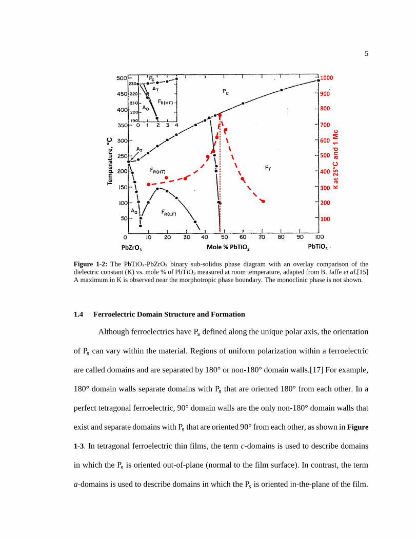
Although ferroelectrics have Ps defined along the unique polar axis, the orientation
of Ps can vary within the material. Regions of uniform polarization within a ferroelectric
are called domains and are separated by 180° or non-180° domain walls.[17] For example,
180° domain walls separate domains with Ps that are oriented 180° from each other. In a
perfect tetragonal ferroelectric, 90° domain walls are the only non-180° domain walls that
exist and separate domains with Ps that are oriented 90° from each other, as shown in Figure
1-3. In tetragonal ferroelectric thin films, the term c-domains is used to describe domains
in which the Ps is oriented out-of-plane (normal to the film surface). In contrast, the term
a-domains is used to describe domains in which the Ps is oriented in-the-plane of the film.
Figure 1-2: The PbTiO3-PbZrO3 binary sub-solidus phase diagram with an overlay comparison of the
dielectric constant (K) vs. mole % of PbTiO3 measured at room temperature, adapted from B. Jaffe et al.[15]
A maximum in K is observed near the morphotropic phase boundary. The monoclinic phase is not shown.

6
By switching the direction of the applied electric field, Ps can be switched from -P
to +P, represented by the ferroelectric polarization vs. electric field hysteresis loop (P-E
loop), as shown in Figure 1-4.[18][19] At low applied alternating-current (ac) electric
fields, there is a linear relationship between polarization and field amplitude (segment AB
in the figure). This is an intrinsic response, in which the electric field further displaces the
center of positive and negative charge in domains with Ps parallel to the applied electric
field, resulting in a distortion of the unit cell. If a large enough field is applied, Ps oriented
at an angle to the applied field direction will be reoriented parallel to parallel to the applied
field direction. This is an extrinsic response, resulting in a nonlinear increase in polarization
with the applied electric field (segment BC in the figure). As domains with Ps parallel to
the applied field direction nucleate and grow, domain wall motion occurs. Due to its
piezoelectric properties, a lattice strain can occur during non-180° domains reorientation,
known as ferroelectric/ferroelastic domain reorientation, since domains switch between
dissimilar unit cell dimensions. In contrast, 180° domain reorientation or ferroelectric
domain orientation does not result in changes in strain of the unit cell. Finally, at high
Figure 1-3: The intrinsic and extrinsic response to an applied electric field. The intrinsic response is
associated with the displacement of the central cation parallel to the applied field, resulting in the distortion
of the unit cell. The extrinsic response is the movement of interfaces such as 90° and 180° domain walls in a
tetragonal system.

7
fields, the P-E loop saturates when all domains have been reoriented to the applied electric
field, resulting in a mono-domain material.
1.5 Rayleigh Analysis
The nonlinearity in the relative permittivity along with the hysteresis in the
polarization can be quantified at sub-coercive, alternating current (ac) electric fields using
the Rayleigh law, as shown in Equation 1-7 and 1-8.[20][21]
𝑃(𝐸) = 𝜀0(𝜀𝑖𝑛𝑖𝑡𝑖𝑎𝑙 + 𝛼𝜀𝐸0)𝐸 ±𝛼𝜀
2𝜀0(𝐸0
2 − 𝐸2) 1-7
Figure 1-4: Polarization vs. electric field (P-E) hysteresis loop of a polycrystalline and single crystal
ferroelectric ceramic. The polycrystalline P-E loop was measured on a {001}-textured, 1.11 µm tetragonal
Pb(Zr0.3Ti0.7)O3 thin film. Schematics A-F represent different domain states during a P-E cycle for an
appropriately oriented single crystal with only 180° domain walls present.

8
𝜀𝑟 = 𝜀𝑖𝑛𝑖𝑡𝑖𝑎𝑙 + 𝛼𝜀𝐸0 1-8
Equation 1-7 describes the nonlinear dependence of the polarization (𝑃) on the
driving field (𝐸), where 𝐸 = 𝐸0 sin(𝜔𝑡), 𝐸0is the driving field amplitude, 𝜀𝑖𝑛𝑖𝑡𝑖𝑎𝑙 is the
reversible dielectric Rayleigh coefficient and 𝛼𝜀 is the irreversible Rayleigh coefficient.
𝜀𝑖𝑛𝑖𝑡𝑖𝑎𝑙 arises from the reversible extrinsic contributions as well as the intrinsic
contributions to the permittivity. 𝛼𝜀 is associated with the irreversible movement of
interfaces, i.e. domain walls or phase boundaries over a potential energy barrier within a
random potential energy landscape.[21] The complex potential energy landscape is dictated
by local strains and internal electric fields that exist within the material as a result of defects
and residual stresses, as shown in Figure 1-5. At low applied electric fields, domain walls
oscillate reversible within a deep potential energy minima. If a large enough electric field
is applied, however, the potential energy barrier for domain wall motion can be overcome,
resulting in irreversible movement of domain walls from one minimum to another. To
quantify the irreversible and reversible domain wall motion contributions to the relative
permittivity, the potential energy landscape needs to remain constant, which is typically
achieved by limiting the applied electric field amplitude to half the coercive field (𝐸0 <
0.5 ∗ 𝐸𝑐). Chapter 2 uses Rayleigh analysis to describe the film thickness dependence of
domain wall motion contributions in a clamped, blanket film and how the thickness
dependence changes when the film is released from the substrate. Although Rayleigh
analysis can be used to separate irreversible extrinsic contributions from the overall
response, the technique is unable to differentiate the intrinsic response from the reversible
extrinsic response, and is therefore limited.

9
1.6 X-ray Diffraction
X-ray diffraction (XRD) is used for characterizing a variety of material properties
related to crystallographic structure including phase, orientation, crystallite size, domain
distributions, lattice strain and microstrain. Synchrotron sources offer high brilliance X-
rays and advanced X-ray optics which are useful for irradiating a small volume of material,
such as thin films, or spatially small features, such as electroded features on MEMS
devices. Additionally, synchrotron facilities provide advanced detectors which enable
time-resolved diffraction of crystallographic changes stimulated by external electric fields.
The application of an electric field while measuring XRD patterns in situ can
provide additional information about the electromechanical response in ferroelectric
materials including electric field induced lattice strain and ferroelectric/ferroelastic domain
reorientation. An intrinsic response to an applied electric field will result in lattice strain
and is indicated by the shifting of the peak positions in an XRD pattern. For example, in a
{001} textured tetragonal perovskite ferroelectrics in which only a and c-domains exist,
the peak position of the 00l reflection will decrease to lower 2θ positions (higher d-
Figure 1-5: A diagram of reversible motion of a domain wall within a deep potential energy well and
irreversible motion of a domain wall within a shallow potential energy well within a potential energy
landscape of a ferroelectric material.

10
spacing); whereas that of the h00 reflection will increase to higher 2θ positions (lower d-
spacing) during application of an electric field oriented normal to the film surface, as shown
in Figure 1-6. These peak shifts correspond to the increase of the out-of-plane d-spacing of
the c-domains and the decrease of the out-of-plane d-spacing of the a-domains in response
to the applied electric field.
An extrinsic response to an applied electric field will result in ferroelastic domain
reorientation and is indicated by the change in integrated peak intensity. For a {001}
textured tetragonal perovskite ferroelectrics in which only a and c-domains exist,
ferroelastic 90° domain reorientation (𝜂002) can be calculated as the electric field induced
change in the volume fraction of c-domains in the direction normal to the film surface
(𝜈002), as shown in Equation 1-9.
Figure 1-6: (a) An XRD pattern showing the change in the 002 and 200 peak position during application of
an electric field for a {001}-textured, 1.11 µm tetragonal Pb(Zr0.3Ti0.7)O3 thin film. (b) A complimentary
schematic showing the change in the out-of-plane d-spacings of a and c-domains during application of
electric field in the out-of-plane direction with crystallographic representations of the d-spacings with respect
to the spontaneous polarization direction (c). The dashed lines in (b) correspond to the original shape. The
red dashed lines in (c) correspond to the original shape.

11
𝜂002 = 𝜈002 − 𝜈0020𝑓𝑖𝑒𝑙𝑑
1-9
𝜈002 is determined from the integrated intensities of the 002 and 200 reflections, using
Equation 1-10.[22][23]
𝜈002 =
𝐼002
𝐼002′
𝐼002
𝐼002′ + 2
𝐼200
𝐼200′
1-10
The term 𝐼ℎ𝑘𝑙 represents the integrated intensity of the hkl reflection where 00l
represents c-domain reflections and h00 represents a-domain reflections. 𝐼ℎ𝑘𝑙′ represents
the reference intensity from the powder diffraction file (𝐼002′ =109 and 𝐼200
′ =249 for PZT
30/70).[24]
XRD can be coupled with Rayleigh analysis to deconvolute the intrinsic
contributions from the reversible, extrinsic contributions to the relative permittivity
represented in the reversible Rayleigh coefficient 𝜀𝑖𝑛𝑖𝑡𝑖𝑎𝑙. Based on the volume fraction of
a-domains and c-domains measured during XRD, intrinsic relative permittivity values can
be calculated using Equation 1-11 which accounts for the inherent dielectric anisotropy of
a tetragonal PZT film.
𝜀𝑟,𝑖𝑛𝑡𝑟𝑖𝑛𝑠𝑖𝑐 = 𝜈200 ∗ (𝜒11 + 1) + 𝜈002 ∗ (𝜒33 + 1) 1-11
In this equation, 𝜈002 is the volume fraction of c-domains determined from
diffraction measurements. The free dielectric susceptibility values were taken from
reference [25]. The reversible, extrinsic contributions to the relative permittivity can be
determined using Equation 1-12, in which 𝜀𝑖𝑛𝑖𝑡𝑖𝑎𝑙0 𝐻𝑧 is the extrapolated reversible Rayleigh
coefficient at 0 Hz.

12
𝜀𝑟,𝑒𝑥𝑡𝑟𝑖𝑛𝑠𝑖𝑐 = 𝜀𝑖𝑛𝑖𝑡𝑖𝑎𝑙0 𝐻𝑧 − 𝜀𝑟,𝑖𝑛𝑡𝑟𝑖𝑛𝑠𝑖𝑐 1-12
The irreversible, extrinsic contributions to the relative permittivity can be determined using
the irreversible Rayleigh coefficient, 𝛼𝜀, as shown in Equation 1-13.
𝜀𝑟,𝑒𝑥𝑡𝑟𝑖𝑛𝑠𝑖𝑐𝑖𝑟𝑟𝑒𝑣𝑒𝑟𝑠𝑖𝑏𝑙𝑒 = 𝛼𝜀𝐸0 1-13
Rayleigh analysis in combination with XRD can quantify the suppression of
extrinsic contributions to the relative permittivity, such as the pinning of domain walls due
to the presence of structural defects and residual stresses. This method is used in Chapter
3 to understand how residual stress and substrate clamping influences the film thickness
dependence of reversible domain wall motions contributions and intrinsic contributions,
individually.
1.7 Residual Stresses in Thin Films
Polycrystalline PZT thin films have suppressed dielectric and piezoelectric
properties compared to their bulk ceramic counterparts. The suppressed properties are in
part due to the residual stresses that develop within the film during processing that limit
electromechanical behavior and ultimately inhibit domain wall motion. As a result, the
extrinsic contributions to the relative permittivity is reduced. The total residual stress (𝜎𝑡𝑜𝑡)
in a film is comprised of both thermal (𝜎𝑡ℎ) and intrinsic (𝜎𝑖) stresses, as shown in Equation
1-14.[26]
𝜎𝑡𝑜𝑡 = 𝜎𝑡ℎ + 𝜎𝑖 1-14
The thermal stress develops upon cooling below the transition temperature from the
paraelectric cubic phase to the room temperature ferroelectric tetragonal phase. 𝜎𝑡ℎ is

13
related to the thermal expansion coefficient mismatch between the film (𝛼𝑓) and the
substrate (𝛼𝑠), as shown in Equation 1-15.
𝜎𝑡ℎ =𝐸𝑓
(1 − 𝜈𝑓)(𝛼𝑓 − 𝛼𝑠)Δ𝑇
1-15
𝐸𝑓 and 𝜈𝑓 are the Young’s modulus and Poisson’s ratio of the film, and Δ𝑇 is the
temperature processing window used during film synthesis. In contrast, intrinsic stresses
are related to microstructural and/or crystallographic flaws such as line defects or non-
stoichiometric defects that form during film deposition and crystallization. In a
PiezoMEMS device such as a cantilever or fixed-fixed beam geometry, residual stress and
thickness of each layer in a multilayered device can have a major impact on the mechanical
and ferroelastic properties of the device, discussed in Chapter 4.
1.8 Scaling Effects
In addition to residual stresses, other factors can contribute to the suppression of
the dielectric and piezoelectric properties in PZT thin films and are exacerbated as film
thickness decreases. The thickness dependent degradation of the piezoelectric and
dielectric properties at small length scales (typically between 10 nm and 1 µm) is known
as scaling effects, as shown in Figure 1-7. Scaling effects can be caused by thickness-
dependent variations in residual stresses, grain size, interfacial passive layers, substrate
clamping, electrode screening, depolarization fields, non-stoichiometric defect
concentrations, domain distributions and domain wall mobility.
[27][28][29][30][31][32][33]

14
Typically, in PZT thin films, a low dielectric permittivity interfacial layer exists at
the film-substrate interface and/or film surface due to lead loss to the substrate and ambient,
respectively, during crystallization. In a thick film, the interfacial layers make up a small
volume fraction of the overall film and have little consequence on the film properties.
Figure 1-7: The thickness dependence of the relative permittivity (εr,33) and piezoelectric coefficient (d33)
measured at room temperature of a variety of ferroelectric materials including polycrystalline and epitaxial
PZT thin films with either morphotropic or tetragonal composition, polycrystalline PLaZT of various
compositions, and other PZT-based and lead-free materials for a variety of processing conditions. Figure
taken from Ihlefeld et al.[34]

15
However, as film thickness decreases, the volume fraction of the thin film that is made of
the low permittivity interfacial layers increases. Since the layers act as capacitors in series,
scaling down the film thickness ultimately degrades the dielectric constant. Grain
boundaries also act as low dielectric regions due to their high concentration of defects and
structural flaws. As film thickness decreases, studies have shown that grain size also
decreases. As a result, the volume fraction of grain boundaries within a thin film increases,
lowering the dielectric constant. Therefore, grain size effects can also exacerbate the
degradation of the dielectric and piezoelectric properties as film thickness decreases. A
comparison of scaling effects associated with grain size vs. interfacial passive layers is
shown in Figure 1-8.
Due to the electromechanical nature of ferroelectrics, the factors that contribute to
scaling effects are often interconnected. For example, variations in residual stresses can
result in variations in domain distributions. PZT thin films processed on Si substrate are
under tensile residual stresses due to the thermal expansion coefficient mismatch between
the film and the substrate. The tensile residual stress forms upon cooling below the
Figure 1-8: (a) A diagram of the low dielectric permittivity regions (light blue) along the film-substrate
interface, film surface and grain boundaries within a thin film with columnar grains. As the film thickness or
grain size is scaled down, the volume fraction of the low dielectric permittivity regions increases. (b) and (c)
shows the thickness dependence of the relative permittivity (εr) as a result of the scaling of film thickness and
grain size, respectively. This figure is adapted from Ihlefeld et al.[34]
16
transition temperature of PZT. Therefore, the residual stress dictates the domain
distribution that forms, favoring higher volume fractions of a-domains with the long axis
of the unit cell in the plane of the film to better accommodate the in-plane tensile stress.
Both the in-plane tensile stress and the predominantly a-domain state will suppress the
dielectric and piezoelectric properties of PZT thin films. Residual stresses can
mechanically suppress domain wall motion or domain wall mobility. Additionally, reduced
domain wall densities, due to a predominantly a-domain state, can limit the extrinsic
contributions to the relative permittivity. To minimize or prevent the property degradation
in thin films at small length scales, it is necessary to investigate how these factors influence
each other in order to determine the underlying mechanisms behind scaling effects.

17
Chapter: 2 Thickness Dependent Response of Domain Wall
Motion in Declamped {001} Pb(Zr0.3Ti0.7)O3 Thin Films
Portions of this chapter are reproduced from: L. M. Denis, G. Esteves, J. Walker, J. L. Jones, and
S. Trolier-McKinstry, “Thickness dependent response of domain wall motion in declamped {001}
Pb(Zr0.3Ti0.7)O3 thin films,” Acta Mater., 151, 243-252, (2018).
2.1 Introduction
Ferroelectric thin films such as Pb(ZrxTi1-x)O3 (PZT) have high dielectric and
piezoelectric properties which can be utilized in actuators, sensors, transducers, and energy
harvesters in microelectromechanical systems (MEMS).[4][8] A small film thickness is
necessary when high capacitance density (including thin film multilayer ceramic
capacitors) or low voltage operation is required.[35][36][37] However, thickness-
dependent property degradation limits the extent that the film thickness can be reduced
while maintaining the performance of such devices.[34][38]
Scaling effects are the size-induced degradation of piezoelectric, ferroelectric and
dielectric properties at length scales (typically between 10 nm and 1 μm) exceeding those
associated with the thermodynamic stability limits for a ferroelectric phase (~1
nm).[34][39] Scaling effects in ferroelectric films are caused by: substrate clamping,
residual stresses, dislocations, interfacial passive layers, electrode screening,
depolarization fields, changes in grain size, a higher concentration of defects at the film-
substrate interface, or thickness-dependent changes in the domain wall population and/or
changes in the domain wall mobility.[27][28][29][30][31][32][33] Additionally, scaling
effects can be exacerbated by processing. Conversely, size effects are caused by the

18
suppression of the intrinsic contribution to the material response as length scales approach
the limits of thermodynamic stability for a ferroelectric phase (~1 nm). Examples of
suppressed intrinsic contribution include the reduction of ferroelectric distortions,
polarization, piezoelectric coefficients, and permittivity.
Scaling effects are manifested in the degradation of the longitudinal piezoelectric
coefficient and relative permittivity as a function of film thickness. This phenomenon is
evident for both epitaxial and polycrystalline ferroelectric films of various
compositions.[34] In most Pb-based perovskites, the relative permittivity (𝜀𝑟,33) starts to
decay significantly below a film thickness of ~100 nm; however, in some cases, gradual
decreases in the permittivity start in films as thick as ~1 μm.[40] Since the degradation of
𝜀𝑟,33 occurs at film thicknesses much greater than the ferroelectric stability limit, the
property degradation at these lengths scales is attributed to extrinsic scaling
effects.[41][42] In particular, it is observed that ferroelastic non-180° domain wall motion
is suppressed as thickness decreases.
The nonlinearity in the relative permittivity along with the hysteresis in the
polarization can be quantified at sub-coercive, ac electric fields using the Rayleigh law,
defined in Equation 1-7 and 1-8 of Chapter 1 in this thesis.[20][21] In short, 𝜀𝑖𝑛𝑖𝑡𝑖𝑎𝑙 is the
reversible dielectric Rayleigh coefficient and arises from the reversible extrinsic
contributions as well as the intrinsic contributions to the permittivity. 𝛼𝜀 is the irreversible
Rayleigh coefficient and is associated with the irreversible movement of interfaces, i.e.
domain walls or phase boundaries, over a potential energy barrier within a random potential
energy landscape.[21]

19
Numerous reports on PZT 52/48 [43][44][45][46][47][48] and PZT 30/70 [49]
demonstrate that the 𝛼𝜀 decreases in films of thicknesses below ~1 μm, indicating that the
irreversible domain wall motion contribution to the permittivity is suppressed. These prior
results were obtained for continuous films on rigid substrates. However, in many MEMS
devices, the film is at least partially released. The release state may change the thickness
dependence of 𝛼𝜀 and associated scaling effects, since substrate clamping is known to
suppress the extent of non-180° domain wall motion in ferroelectric thin films.[50][51]
Therefore, there is a need to investigate the influence of substrate clamping on the
thickness-dependent extrinsic contribution to the relative permittivity.
For a fixed film thickness, the clamping of the film can be alleviated in several
ways. First, island structures with high aspect ratios allow the structures to be partially
declamped, thus, increasing 90° domain wall mobility and doubling the remanent
polarization of PZT at high applied electric fields.[50][52] Additionally, piezoelectrically-
active, ferroelectric nanotubes with high aspect ratios have been created via vacuum
infiltration of macroporous Si templates (aspect ratio of >10:1)[10] or a bottom-up
nanomanufacturing method (aspect ratio of 5:1)[53]. The high aspect ratios in these studies
were chosen such that substrate clamping effects could be minimized. Declamping can also
be achieved by releasing diaphragm structures from the underlying substrate.[54][55] The
resulting increase in dielectric properties were attributed to lower potential energy barriers
which allowed enhanced irreversible domain wall motion and an increase in 𝛼𝜀 for the
released film. Synchrotron diffraction of films > 1 μm in thickness demonstrate that
released films show higher levels of non-180° domain reorientation under field.[51]
However, released cantilevers still demonstrate thickness dependent remanent polarization

20
and piezoelectric properties attributed to residual stresses. These residual stresses are
commonly associated with the thermal expansion coefficient mismatch between the film
and the substrate and/or the presence of a thin layer at the film-substrate interface with a
low dielectric constant.[56] In this work, scaling effects have been investigated in PZT
films < 1 µm thick in both clamped and partially released states relevant to MEMS devices.
2.2 Experimental Procedure
2.2.1 Film Synthesis and Nanofabrication
Tetragonal, {001} textured polycrystalline Pb(Zr0.3Ti0.7)O3 (PZT 30/70) thin films
doped with 2% Nb were fabricated via chemical solution deposition (CSD) as described
elsewhere.[57][58] The solution was deposited onto a Pt/TiO2/SiO2/Si stack to produce
films with thickness ranging from 0.27 to 1.11 µm. Prior to the deposition of the film, a
0.08 M PbO layer was spin coated onto the Pt then dried (1 min. at 150°C and 2 min. at
250°C) and pyrolyzed (10 min. at 400°C). This PbO layer was not crystallized. The
underlying layer of PbO provided excess lead at the film-substrate interface which
minimized lead loss to the substrate during crystallization. A commercial PZT-E1 sol-gel
solution (Mitsubishi Materials Corporation, Tokyo, Japan) of composition Pb(Zr0.3Ti0.7)O3
with 10 mol% lead excess, doped with 1 mol% Mn and a concentration of 10 wt% PZT
was used to promote {001} texturing. This solution was deposited onto the PbO layer at
2000 rpm, dried (2 min. at 150°C), pyrolyzed (5 min. at 300°C), and crystallized in a rapid
thermal annealer (RTA) (1 min. at 700°C in flowing O2 gas at 2 SLPM and a ramp rate of
10°C/s). As shown in Figure 2-1, a spin speed of 2000 rpm produced the best {001}
texturing of the seed layer; this corresponds to a seed layer thickness of ~60 nm. Above
21
this critical thickness, {111} texture developed; below this critical thickness, {110} texture
was observed. Similar results have been obtained for seeding of undoped PZT 52/48 films
from Mitsubishi Materials solutions.[59][60]
After crystallization of the seed layer, 0.4M PZT 30/70 sol-gel with 12 mol% lead
excess and doped with 2 mol% Nb was spin coated at either 3000 rpm or 1500 rpm, dried
(2 min. at 250°C), pyrolyzed (5 min. at 400°C), crystallized in the RTA (1 min. at 700°C
in flowing O2 gas at 2 SLPM and a ramp rate of 10°C/s) and repeated until the desired
overall film thickness was obtained. To obtain high quality films with similar grain size
distributions, the processing conditions were optimized for the desired film thickness as
needed. As the overall film thickness decreases, the number of deposited layers must be
decreased to keep the spin speed and layer thickness constant. However, as the number of
deposited layers decreases, there is an increased probability of forming a pin hole in the
film which will result in a decreased electrode yield. To combat this, the number of
Figure 2-1: X-ray diffraction patterns depicting the dependence of the preferred orientation of the 1% Mn-
doped PZT 30/70 Mitsubishi Materials seed layer on the spin rates for chemical solution deposition.

22
deposited layers was increased in thinner films (< 0.56 µm thick). Increasing the spin speed
from 1500 rpm to 3000 rpm decreased the thickness of each layer and allowed more layers
to be deposited for a given film thickness. This method was also employed by Bastani et
al. to obtain thin insulating PZT films.[29] Figure 2-2 shows a schematic of the thickness
series. The long pyrolysis step enabled the growth of high-density films with lateral grain
sizes of 50-150 nm, as shown in the field emission scanning electron microscopy (FESEM)
images in Figure 2-3.
Figure 2-2: Schematic of the layer-by-layer crystallization steps used to grow PZT 30/70 thin films ranging
in thickness from 0.27 μm to 1.1 μm for (a) films doped with 2% Nb and (b) films doped with 1% Mn. The
cross section of the Pt/PZT/Pt/TiO2/SiO2/Si stack is also shown.
Figure 2-3: Top-down micrographs of PZT 30/70 thin films for thickness ranging from 0.27 μm to 1.1 μm
showing the distribution of grain sizes. A cross-sectional micrograph of the 0.56 μm PZT thin film on a Pt
electrode illustrating columnar grain growth of the film. There is no evidence of porosity or secondary phases.

23
To provide excess lead to the surface of the film, after every 5 crystallized layers
of PZT 30/70, a 0.08M PbO layer was spin coated at 6000rpm, dried (1 min. at 150°C and
2 min. at 250°C) and crystallized in the RTA (1 min. at 700°C in 2 SLPM O2 gas at a ramp
rate of 10°C/s). The PbO crystallization steps are also shown in Figure 2-2, labeled as ‘PbO
cap’. This converted lead-deficient surface pyrochlore (or fluorite) phases to the desired
perovskite phase[61], and improved {001} texturing for both series of samples.
Large area platinum top electrodes (3.5 mm x 0.7 mm) were defined
photolithographically and sputtered onto the PZT using RF magnetron sputtering. Part of
the electroded area of the films was released from the substrate by dry etching 600 μm x
146 μm pits through the Pt/PZT/Pt/TiO2/SiO2 stack using an Ulvac NE-550 inductively
coupled high-density plasma etch tool. The exposed Si substrate was then etched via an
isotropic Xactic XeF2 e1 vapor etch tool until a 100 μm diameter trench was formed, as
discussed elsewhere.[51][54] The conditions of the etch recipes for these two steps are
listed in Table 2-1. The sample was annealed at 400°C for 30 minutes before and after the
XeF2 etch step to remove residual moisture and reduce etch damage. The density of the
etch pits within one electroded area dictated the percent of electroded area that was released
from the substrate (fully clamped or 0% released, 25% released, 50% released and 75%
released), as illustrated in Figure 2-4 (a). The suspended electroded area above the trench
represents a declamped region of the film, as shown in Figure 2-4 (b). An optical
microscope image of the top down view of a released electrode and a cross-sectional
FESEM micrograph of the released Pt/PZT/Pt/TiO2/SiO2 stack suspended above the etch
trench are shown in Figure 2-4 (c) and (d), respectively.
Table 2-1: Etch conditions for released structures

24
Material Chamber Pressure Gas Chemistry Forward Power Etch Rate
Pt/PZT/Pt/TiO2 5 mTorr 30 sccm Cl2
40 sccm Ar
300 W at MHz
0 W at MHz
Pt: 1,500 sec/μm
PZT: 300 sec/μm
SiO2 5 mTorr 50 sccm CF4 300 W at MHz 240 sec/μm
Si 2 mTorr XeF2 - 6 sec/μm
Figure 2-4: (a) A top down view of the Pt electrode for each release state: clamped or 0% released, 25%
released, 50% released and 75% released. The different degrees of release were achieved by varying the
density of the etch pits within one electroded region. (b) 3-D cross-sectional schematics of the release
structures including the etch pits that run vertically through the Pt/PZT/Pt/TiO2/SiO2 stack and the 100 μm
diameter etch trench that was undercut into the Si substrate below each etch pit region (not to scale). (c) An
optical microscope image of the top down view of part of a released electrode and (d) a cross-sectional
micrograph of the released Pt/PZT/Pt/TiO2/SiO2 stack suspended above the etch trench.

25
2.2.2 Characterization
The orientation and phase of the film was determined from X-ray diffraction (XRD)
patterns taken using a lab source diffractometer (PANalytical Empyrean), as shown in
Figure 2-5 (a, b). Lotgering factors ranged from 90% to 100% depending on the film
thickness, with Lotgering factors closer to 100% for films below ~0.5 µm. The volume
fraction of c-domains (𝜈002) of a sample in the as-processed state was calculated from the
integrated intensities of the 002 and 200 XRD peaks using LIPRAS (Line-Profile Analysis
Software).[62] An example of the peak fitting for the 1.1 µm film is shown in Figure 2-5
(c) and the corresponding normalized 𝜈002 values are shown in Figure 2-5 (d). The peaks
were fit using an asymmetric Pearson VII function which takes into account the peak
asymmetry and approximates the diffuse scattering.[63]

26
𝜈002 was calculated using Equation 1-10, as described in Chapter 1 of this
thesis.[22][23] By using the ratio of integrated intensities over a reference intensity, the
structure factors for the 002 and 200 reflections in a tetragonal system are accounted for.
Error of 𝜈002 was calculated using an error propagation method that accounts for the
integrated intensity error generated from peak fitting using LIPRAS.
Polarization vs. electric field (P–E) hysteresis loops were measured at a frequency
of 10 Hz using a Radiant Precision Ferroelectric Tester for both clamped films and 75%
released films. Further electrical characterization in the form of Rayleigh analysis was
Figure 2-5: Phase pure X-ray diffraction patterns of tetragonal {001} textured PZT 30/70 thin films doped
with 2% Nb and thicknesses ranging from 0.27 μm to 1.1 μm (a, b). The peak fitting of the 002/200 peaks
for the 1.1 μm film is shown (c). The normalized volume fraction of c-domains (ν002) is also shown as a
function of film thickness (d). Note: error bars are smaller than the symbol size.

27
conducted on both clamped and released films at frequencies ranging from 50 Hz to 4 kHz
with applied AC electric fields up to 0.5*Ec (where Ec is the coercive field). These
measurements were taken using a Hewlett Packard 4284A LCR meter. The samples were
subject to an anneal at 400°C for 30 min. and an aging time of 24 hours prior to the Rayleigh
measurements. The aging process was consistent across all samples prior to Rayleigh
analysis. Error was calculated using an error propagation method that accounts for the error
associated with a 95% confidence interval of the linear fit of the Rayleigh parameter as a
function of applied AC electric field.
2.2.3 Capacitor in Series Model
To minimize the influence that the seed layer has on the Rayleigh analysis, a
capacitor in series model was applied to the permittivity data, as shown in Equation 2-1 in
terms of capacitance (C) and Equation 2-2 in terms of the dielectric constant (k).
1
𝐶=
1
𝐶𝑓+
1
𝐶𝑠
2-1
𝑘
𝑡=
𝑘𝑓
𝑡𝑓+
𝑘𝑠
𝑡𝑠
2-2
where C represents the measured capacitance, Cs is the measured capacitance of the seed layer, Cf
is the capacitance of the balance of the ferroelectric film and t is the total
thickness.[29][64][65][66][67] Cs was not extracted from a linear relationship between C-1 vs. film
thickness at zero thickness. Since the volume fraction of c-domains is not constant as a function of
film thickness, the standard extrapolation will not accurately predict the interface capacitance, since
it does not account for the thickness-dependent change of domain state. Rather, Cs is the capacitance

28
of the seed layer, measured as a function of ac electric field for frequencies ranging from 50 to
4,000 Hz, as shown in Figure 2-6 (a). Dispersion curves of the Rayleigh parameters for the seed
layer are also reported in Figure 2-6 (b-c). The seed layer has a dielectric constant of 510 (measured
at 1 kHz and 30 mV), which is ~ 25% less than that of the 0.35 μm PZT film of the same
composition and measurement conditions. To check the quality of the Mitsubishi Materials solution
used for the seed layer, a 0.38 μm thick film was grown using this solution. The measured Rayleigh
parameters of the Mitsubishi Materials 0.38 μm film were comparable to that of a 2-MOE-based
sol gel film of 0.38 μm thickness, as shown in Figure 2-6, for the same composition and a common
seed layer. This comparison indicates that the suppressed properties of the 0.06 μm seed layer,
shown in Figure 2-6 (b-c), are due to scaling effects.
Figure 2-6: (a) Measured relative permittivity vs. a.c. field and (b) frequency dispersion of the Rayleigh
parameter αε and εinitial for clamped the seed layer of 0.06 μm thickness and 1% Mn-doped PZT 30/70
composition. The frequency dispersion of the Rayleigh parameter αε (c) and εinitial (d) for clamped 0.38-0.35

29
2.3 Results
2.3.1 Thickness Dependence of Polarization Hysteresis in Declamped Films
Figure 2-7 shows the P-E loops for the 2% Nb-doped PZT 30/70 thickness series.
The coercive field (Ec) ranges from 54 to 63 kV/cm. The films exhibited remanent
polarization (Pr) values ranging from 11 to 18 𝜇𝐶/𝑐𝑚2. Pr is defined here to be the
polarization remaining in the material when the electric field is reduced to zero after
applying a maximum electric field of 400 kV/cm in the positive electric field direction. The
relatively small polarizations are a result, in part, of the largely a-domain state of the films
resulting from the thermally induced tensile stress state of the PZT film grown on a Si
substrate.[68] In general, as film thickness increases, the maximum polarization (Pmax) and
Pr increase, characteristic of the scaling effect. Upon release, Pr and Pmax both increase for
a given thicknesses, as shown in Figure 2-8 for (a) 1.11, (b) 0.38 and (c) 0.27 μm 2% Nb-
doped films. This is most clearly seen in Figure 2-8 (b), which shows the changes in the P–
E loop of 0.38 μm film for each release state (0%, 25%, 50% and 75%). Interestingly, the
thinnest film (0.27 μm) shows the smallest increase in Pr after being 75% released from the
substrate. This suggests that other mechanisms are involved in pinning domains in the film
(e.g., potentially higher defect concentrations, higher grain boundary concentrations, or
higher residual stresses in the film that are not relieved upon release).
μm 1% Mn-doped PZT 30/70 films grown using PSU-made sol gel compared to a clamped 0.35 μm 1% Mn-
doped PZT 30/70 film grown using Mitsubishi Materials solution is also shown. The Mitsubishi Materials
solution was exclusively used for growth of the 0.06 μm seed layer.

30
Figure 2-7: Polarization vs. electric field hysteresis loops of clamped 2% Nb-doped PZT 30/70 thin films of
varying thickness ranging from 0.27 μm to 1.1 μm.

31
2.3.2 Irreversible Contributions to Permittivity
2.3.2.1 Thickness Dependence in Clamped Films
Rayleigh analysis was used to characterize extrinsic contributions to the relative
permittivity in the form of irreversible domain wall motion. For clamped Nb-doped films,
Figure 2-8: The change in P–E hysteresis loops of 2% Nb-doped PZT 30/70 thin films between the clamped
and 75% released states for (a) 1.11 μm, (b) 0.38 μm, and (c) 0.27 μm thick films. The evolution of the P–E
loop for the 0.38 μm thick film is also shown for clamped, 25%, 50% and 75% released states.

32
the irreversible contribution to the permittivity, 𝛼𝜀, decreases as film thickness decreases
with thickness ranging from 1.11 μm to 0.27 μm. This thickness dependence of 𝛼𝜀 is shown
in Figure 2-9 (a).
Rayleigh parameters of the PZT film, after application of the capacitor-in-series
model, were calculated for each film thickness. For simplicity, the Rayleigh parameters
prior to applying the capacitor in series model are labeled as ‘Seed + Film’ in Figure 2-9
(a), and the data after applying the capacitor in series model are labeled as ‘Film’ in Figure
2-9 (b). For the Nb-doped films, the seed layer has a large effect on the irreversible Rayleigh
coefficient. The 𝛼𝜀 for the PZT film alone is 51% larger than the 𝛼𝜀 measured for the film
in series with the seed layer. The difference in 𝛼𝜀 occurs over the entire frequency range
for each film thickness.
Without the influence of the seed layer, 𝛼𝜀 values for the 1.11 and 0.56 μm films
converge, which suggests that these films have comparable domain wall pinning effects.
Figure 2-9: Frequency dispersion of the Rayleigh parameter αε as a function of film thickness ranging from
0.27 μm to 1.1 μm for PZT 30/70 thin films doped with 2% Nb in the clamped state before applying the
capacitor in series model (Seed + Film) (a), in the clamped state after applying the model (Film) (b) and in
the 75% released state after applying the model (c).

33
However, the thickness dependence of 𝛼𝜀 is still present in thicknesses below 0.56 μm.
Additionally, the 𝛼𝜀 values for the 1.11 and 0.56 μm films are lower than those for 0.38
and 0.27 μm films at low frequencies. The origin of this difference is unknown but could
be related to a difference in stress level associated with the domain state, as discussed in
Chapter 3 of this thesis.
2.3.2.2 Thickness Dependence in Released Films
To assess whether the suppression of 𝛼𝜀 is influenced by substrate clamping,
Rayleigh parameters were obtained for films that were partially released from the substrate.
Prior to the Rayleigh measurements, the films were subject to high applied electric fields
(up to 3*Ec) to induce tearing of the diaphragms and create globally released regions.[51]
All films exhibited tearing of the diaphragms with variations in the number of tears and the
angle of the tear with respect to the horizontal length of the etch pits. However, most
electrodes have one tear at each end of the diaphragm regardless of film thickness. The tear
typically occurs at the curved ends of the rounded, beam-like etch pits and propagates
horizontally towards the electrode edges, shown in the FESEM micrograph of Figure 2-10.
In situ synchrotron XRD measurements confirm that, upon global release, enhanced
ferroelastic reorientation occurs in PZT 30/70 thin films compared to either local released
or clamped states. The enhanced properties in a globally released film are due to the
reduction in the average, global tensile stress of the film.[51] After global release, all
samples were annealed at 400°C for 30 min. and aged for 24 hours prior to Rayleigh
analysis.

34
To isolate the influence of substrate clamping on the thickness dependence, the
trends in 𝛼𝜀 were analyzed for a 75% released film after applying the capacitor in series
model. Upon 75% release, 𝛼𝜀 increases by up to 23%, with larger changes for the thinner
films, shown in Figure 2-9 (c) for Nb-doped films. Additionally, the evolution of 𝛼𝜀 with
increasing release state is shown for 0.27 μm 2% Nb-doped film in Figure 2-11.
Figure 2-10: A micrograph of the torn electroded regions extending from the etch pit after global released.

35
2.3.3 Frequency Dependence of αε
After applying the capacitor in series model to a clamped Nb-doped film, the
greatest increase in 𝛼𝜀 occurs at low frequencies, shown in Figure 2-12. This indicates that
changes in 𝛼𝜀 are also frequency-dependent as well as thickness-dependent. The frequency
dependence (B𝛼𝜀) of the Rayleigh coefficient 𝛼𝜀 was extracted from fits to Equation 2-3.
𝛼𝜀 = 𝛼𝜀,𝑖 − 𝐵𝛼𝜀log 𝑓 for frequencies in Hz 2-3
The frequency dependence in 𝛼𝜀 is unknown, but it is speculated that it may be
related to the differences in the mobility of domain wall clusters of different sizes. Domain
walls tend to move in clusters;[45][54] larger clusters may be active at lower frequencies.
As frequency rises, the size of the responding cluster may drop. This would account for the
frequency dependence in 𝛼𝜀 at these comparatively low frequencies, as shown in Figure
Figure 2-11: Frequency dispersion of the Rayleigh parameter αε as a function of release state including
clamped or 0% released, 25% released, 50% released and 75% released from the substrate for 0.27 μm thick
PZT 30/70 thin film doped with 2% Nb.
Figure 2-12: Frequency dependence (B) of the Rayleigh parameter αε as a function of film thickness for PZT
30/70 thin films doped with 2% Nb (a) for the clamped state before applying the capacitor in series model
(Seed + Film), the clamped state after applying the model (Film), and the 75% release state after applying
the model. The dashed and dotted boxes represent values of B(αε) for the 0.27 and 0.56 μm films, respectively.
Complementary frequency dispersion of the Rayleigh parameter αε are also shown for thickness 0.27 μm (b)
and 0.56 μm (c).

36
2-12. It is notable that the frequency dependence observed here at well below the ~1 – 10
GHz range at which motion of individual domain walls would be expected to freeze out.
After applying the capacitor in series model, B𝛼𝜀 increases, shown in Figure 2-12
(a) for Nb-doped films. Additionally, larger changes in B𝛼𝜀 are observed for films below
0.5 μm in thickness. This is highlighted in the comparison between the 0.27 μm and 0.54
μm films, shown in Figure 2-12 (b-c). A ~ 69% increase in the frequency dependence of 𝛼𝜀
occurs for a 0.27 μm Nb-doped film (b) compared to a ~ 8% increase for 0.56 μm Nb-
doped film (c).
Upon 75% release from the substrate, B𝛼𝜀 increases further for all film thicknesses,
as shown in Figure 2-12 (a) for Nb-doped films. Upon release, a greater increase in 𝛼𝜀
occurs at low frequencies, resulting in an increase in B𝛼𝜀. However, the change in B𝛼𝜀
upon
release does not vary greatly with film thickness.
2.3.4 Intrinsic and Reversible Contributions to Permittivity
2.3.4.1 Thickness Dependence in Clamped Films
The thickness dependence in the intrinsic response and the reversible contributions
to the dielectric response is represented in the Rayleigh parameter 𝜀𝑖𝑛𝑖𝑡𝑖𝑎𝑙. For clamped
Nb-doped PZT films, 𝜀𝑖𝑛𝑖𝑡𝑖𝑎𝑙 varies non-monotonically as a function of film thickness,
shown in Figure 2-13 (a), presumably because of differences in the film domain state. The
volume fraction of c-domains (𝜈002) increases as film thickness increases from 0.27 to 1.11
μm for 2% Nb-doped films, as shown in Figure 2-5 (d). This higher concentration of c-
domains in thicker films is consistent with findings from the literature.[69] The resulting

37
decrease in the intrinsic contribution to the relative permittivity is reflected in the decrease
in the 𝜀𝑖𝑛𝑖𝑡𝑖𝑎𝑙 above 0.38 μm.
Rayleigh parameters for clamped, Nb-doped PZT films without the influence of the
seed layer are shown in Figure 2-13 (b). 𝜀𝑖𝑛𝑖𝑡𝑖𝑎𝑙 increases after the applying the capacitor
in series model by up to 13%. 𝜀𝑖𝑛𝑖𝑡𝑖𝑎𝑙 values for the 0.56, 0.38 and 0.27 μm films approach
convergence, suggesting that the films have comparable domain populations, as well as
comparable reversible domain wall contributions to 𝜀𝑖𝑛𝑖𝑡𝑖𝑎𝑙. However, the 1.11 μm film
maintains much lower 𝜀𝑖𝑛𝑖𝑡𝑖𝑎𝑙 values due to the greater volume fraction of c-domains.[70]
2.3.4.2 Thickness Dependence of Released Films
Figure 2-13 (c) shows the influence of 75% release on 𝜀𝑖𝑛𝑖𝑡𝑖𝑎𝑙 for the thickness series
of Nb-doped films. Upon release, 𝜀𝑖𝑛𝑖𝑡𝑖𝑎𝑙 decreases as film thickness increases from 0.27
to 1.11 μm. This thickness dependence of 𝜀𝑖𝑛𝑖𝑡𝑖𝑎𝑙 for the 75% released film is influenced
by intrinsic contributions, i.e. the change in volume fraction of c-domains as a function of
thickness, since an increasing volume fraction of c-domains will decrease the permittivity.
Figure 2-13: Frequency dispersion of the Rayleigh parameter εinitial as a function of film thickness ranging
from 0.27 μm to 1.1 μm for PZT 30/70 thin films doped with 2% Nb in the clamped state before applying the
capacitor in series model (Seed + Film) (a), in the clamped state after applying the model (Film) (b) and in
the 75% released state after applying the model (c).

38
Interestingly, 𝜀𝑖𝑛𝑖𝑡𝑖𝑎𝑙 decreases with increasing release state for a given film
thickness, as shown in Figure 2-14 for the 0.27 μm film doped with 2% Nb. It has previously
been reported that the release process itself does not change the volume fraction of c-
domains at zero applied electric field.[51] Therefore, the observed decrease in 𝜀𝑖𝑛𝑖𝑡𝑖𝑎𝑙 upon
release may suggest that there is a shift of at least some of the domain walls from reversible
motion in a clamped film to irreversible motion in a released film.
2.3.5 Frequency Dependence of εinitial
Removing the influence of the seed layer by applying the capacitor in series model
produces little to no change in B𝜀𝑖𝑛𝑖𝑡𝑖𝑎𝑙, regardless of film thickness, as shown in Figure
2-15. Upon 75% release from the substrate, there is little to no change in B𝜀𝑖𝑛𝑖𝑡𝑖𝑎𝑙, regardless
of film thickness, also shown in Figure 2-15. Notably, the changes in B𝛼𝜀 upon release
exceed changes in B𝜀𝑖𝑛𝑖𝑡𝑖𝑎𝑙. The frequency dependence of nonlinearity for 𝛼𝜀 and 𝜀𝑖𝑛𝑖𝑡𝑖𝑎𝑙
Figure 2-14: Frequency dispersion of the Rayleigh parameter εinitial as a function of release state including
clamped or 0% released, 25% released, 50% released and 75% released from the substrate for 0.27 μm thick
PZT 30/70 thin film doped with 2% Nb.

39
are listed in Table 2-2 and Table 2-3, respectively, for all film thicknesses in the clamped
state before the capacitor in series model was applied, the clamped state after the model
was applied and the 75% release state after the model was applied.
Table 2-3: Frequency dependence of Rayleigh parameter εinitial
Thickness
(μm)
Clamped (Seed + Film) Clamped (Film) 75% Released (Film)
A B A B A B
1.11 727 ± 2.4 19.3 ± 0.9 742 ± 2.7 19.8 ± 1.1 698 ± 1.6 19.0 ± 0.6
0.56 793 ± 0.9 20.7 ± 0.3 843 ± 1.5 19.1 ± 0.5 800 ± 2.3 24.1 ± 0.8
0.38 805 ± 1.8 20.3 ± 0.6 879 ± 1.8 22.0 ± 0.6 812 ± 1.4 23.0 ± 0.5
0.27 766 ± 1.2 19.6 ± 0.4 866 ± 2.1 22.3 ± 0.7 813 ± 1.7 20.8 ± 0.6
Figure 2-15: Frequency dependence (B) of the Rayleigh parameter εinitial as a function of film thickness for
PZT 30/70 thin films doped with 2% Nb for the clamped state before applying the capacitor in series model
(Seed + Film), the clamped state after applying the model (Film) and the 75% release state after applying the
model.
Table 2-2: Frequency dependence of Rayleigh parameter αε (cm/kV)
Thickness
(μm)
Clamped (Seed + Film) Clamped (Film) 75% Released (Film)
A B A B A B
1.11 12.7 ± 0.06 1.3 ± 0.02 13.8 ± 0.07 1.4 ± 0.03 15.8 ± 0.12 1.9 ± 0.04
0.56 12.4 ± 0.11 1.3 ± 0.03 13.8 ± 0.19 1.4 ± 0.06 16.8 ± 0.22 1.9 ± 0.07
0.38 12.7 ± 0.13 1.6 ± 0.04 16.6 ± 0.19 2.0 ± 0.06 19.4 ± 0.19 2.4 ± 0.06
0.27 10.8 ± 0.18 1.3 ± 0.06 16.3 ± 0.32 2.2 ± 0.11 20.0 ± 0.36 2.8 ± 0.12

40
2.4 Discussion
2.4.1 Capacitor-in-Series Model
The difference in 𝛼𝜀 (∆𝛼𝜀) between the total measured response and the response
after applying a capacitor in series model represents the decoupling of the film properties
and the seed layer properties, as shown in Figure 2-16 (a). The increase in 𝛼𝜀 after applying
the model suggests that the seed layer contributes directly to the pinning of irreversible
domain walls and/or it reduces the field across the balance of the film (which
commensurately reduces the domain wall contributions to the properties). Defect dipoles
associated with the Mn doping of the seed layer PZT solution, such as 𝑀𝑛𝑇𝑖′′ −
𝑉𝑂∙∙ 𝑜𝑟 𝑀𝑛𝑇𝑖
′ − 𝑉𝑂∙∙, are assumed to be present and create internal electric fields that pin
domain walls. Additionally, larger increases in 𝛼𝜀 were observed for the thinner films
which are more influenced by the seed layer properties in which the seed layer makes up a
larger fraction of the total thickness.

41
For the 1.11 and 0.56 μm films, ∆𝛼𝜀 is larger at lower frequencies compared to
higher frequencies, relating to an increase in B𝛼𝜀. A larger ∆𝛼𝜀 at lower frequencies
indicates that the seed layer preferentially influences the mobility or density of slower
moving irreversible domain walls that are active at lower frequencies. In contrast, ∆𝜀𝑖𝑛𝑖𝑡𝑖𝑎𝑙
does not vary as a function of frequency, as shown in Figure 2-16 (c). ∆B𝜀𝑖𝑛𝑖𝑡𝑖𝑎𝑙 are
representative of changes in the reversible domain wall contributions, as intrinsic
contributions should be constant in this frequency range. Therefore, the lack of change in
Figure 2-16: The change in the Rayleigh parameters αε (a-b) and εinitial (c-d) as a function of film thickness
for PZT 30/70 thin films doped with 2% Nb. (a, c) Represents the change after applying the capacitor in
series model. (b, d) Represents the change upon release.

42
B𝜀𝑖𝑛𝑖𝑡𝑖𝑎𝑙 compared to that for B𝛼𝜀
indicates that the seed layer has a greater impact on
irreversible domain wall motion compared to reversible domain wall motion.
2.4.2 Substrate Clamping Effects
In general, 𝛼𝜀 increases upon 75% release from the substrate. It is proposed that the
potential energy barrier for irreversible domain wall motion decreases upon release, the
concentration of pinning sites due to substrate clamping decreases upon release which
allows for an increase in domain wall motion, or the mobility of existing domain walls
increase. ∆𝛼𝜀 upon release is greater for thinner films compared to thicker films, as shown
in Figure 2-16 (b). Strain relaxation upon release from the substrate could be a possible
explanation for this trend. Due to the thermal expansion coefficient mismatch between the
PZT film and the Si substrate, an in-plane tensile strain in the PZT film develops upon
cooling, with a greater amount of thermally-induced strain reported in thinner films
compared to thicker films.[33][71] Variations in the thermal strain as a function of film
thickness could also explain the observed change in 𝜈002 of a clamped film as film
thickness increases.
Additionally, ∆𝛼𝜀 is larger at lower frequencies compared to higher frequencies, as
reflected by an increase in B𝛼𝜀 upon release. This confirms that substrate clamping also
preferentially influences the mobility or density of slower moving irreversible domain
walls, contributing to the suppression of B𝛼𝜀. Upon release, either the mobility of the
existing domain walls active at lower frequencies rises, or some of the slower moving
domain walls are depinned. This is not the case for reversible domain wall motion

43
contributions. Upon release, ∆𝜀𝑖𝑛𝑖𝑡𝑖𝑎𝑙 does not vary as a function of frequency, as shown
in Figure 2-16 (d). Since the changes in frequency dependence are representative of changes
in the reversible domain wall motion contributions, substrate clamping also has a greater
impact on irreversible domain wall motion compared to reversible domain wall motion.
2.5 Conclusions
Rayleigh analysis was used to investigate the influence of substrate clamping on
the extrinsic contribution to the relative permittivity of PZT thin films doped with 2% Nb
for a film thickness range of 0.27 μm to 1.1 μm. These results indicate that both the seed
layer and substrate clamping accounted for a substantial apparent suppression of the
extrinsic contribution to the relative permittivity. It was found that irreversible domain
wall motion contributions to the relative permittivity (𝛼𝜀) decrease as film thickness
decreases, consistent with findings in the literature. The suppression of 𝛼𝜀 is partially
recoverable by (1) removing the influence of the seed layer via a capacitor in series model
and (2) reducing the substrate clamping. The need for a capacitor in series model to account
for the seed layer properties will depend explicitly on processing conditions and, therefore,
should always be checked. After removing the influence of a Mn-doped seed layer, the 𝛼𝜀
for the PZT film alone is 51% larger than the 𝛼𝜀 measured for the film in series with the
seed layer; this is attributed to the film having a higher irreversible domain wall motion
contribution to the permittivity compared to the seed layer. Upon 75% release from the
substrate, 𝛼𝜀 increased further by up to 23%. Finally, the frequency dependence of 𝛼𝜀
increases upon release due to depinning of slower moving irreversible domain walls.

44
Chapter: 3 Residual Stress and Ferroelastic Domain
Reorientation in Declamped {001} Pb(Zr0.3Ti0.7)O3 Films
3.1 Introduction
Ferroelectric materials are utilized in applications such as actuators, sensors and
nonvolatile memory.[3] Typically, the dielectric and piezoelectric responses in
ferroelectric thin films are suppressed relative to their bulk counterparts due to a
combination of small grain sizes, thermal strains, clamping due to the substrate, and the
potential for a high concentration of defects. [33][38][34][72][73][74]
In ferroelectrics, residual stresses can dictate preferred domain distributions.[75] In
many ferroelectric films, the substrate has a strong influence on the domain
configuration.[76] For example, preferential out-of-plane polarization can be achieved for
relaxed, tetragonal Pb(Zrx,Ti1-x)O3 (PZT) films grown on sapphire, MgO or LaAlO3, which
have a larger coefficient of thermal expansion compared to PZT. [74][75][76][77] This
type of domain configuration is ideal for applications such as FeRAM which utilize out-
of-plane polarization switching for memory.[78]
Since the coefficient of thermal expansion (𝛼𝐶𝑇𝐸) of Si (2.6 ppm/°C) is less than
that of PZT in the paraelectric phase (6.7-9.4 ppm/°C depending on composition),[75] PZT
films processed on Si are under an in-plane tensile stress, favoring orientation of the
spontaneous polarization in-plane (e.g. producing preferentially a domain, rather than c
domain films).[77][79] Moreover, local stresses can form at the film-bottom electrode
interface that differ from the average residual stress, complicating the understanding.
Griggio et al. proposed that these local strains can be partially relieved by removing the

45
film from the substrate.[54] The residual stress state of PZT films on Si is also reported to
depend on the number of deposited layers or film thickness [30] and is correlated with
variations in domain patterns.[31][80] The apparent variation in the stress state as a
function of film thickness may also be associated with changes in the stress state of the
underlying thermal oxide layer or Pt-bottom electrode during subsequent
annealing.[81][82]
Differences in the intrinsic and extrinsic contributions to the relative permittivity
(𝜀𝑟) will result from differences in the domain orientation state, domain wall densities, and
the mobility of domain walls. This, in turn, contributes to the apparent scaling effects in
the functional properties.[29][34][83] For example, PZT films which have predominately
a-domains will have a larger out-of-plane intrinsic contribution to 𝜀𝑟, possibly at the
expense of a reduced 90° domain wall density and reduced extrinsic contributions to
𝜀𝑟.[76] Therefore, variations in the in-plane stress state of PZT films can result in a
thickness dependence in the domain state, intrinsic contributions and extrinsic
contributions to 𝜀𝑟.
The differences in the intrinsic and extrinsic contributions to 𝜀𝑟 can often be
quantified using Rayleigh analysis.[43][47][49][83][84] The Rayleigh law is described in
Equation 1-7 of Chapter 1 in this thesis. In short, 𝜀𝑖𝑛𝑖𝑡𝑖𝑎𝑙 is the reversible dielectric Rayleigh
coefficient and represents the sum of reversible extrinsic and intrinsic contributions to the
permittivity. 𝛼𝜀 is the irreversible dielectric Rayleigh coefficient associated with extrinsic
contributions to the permittivity from irreversible movement of domain walls and phase
boundaries through a random potential energy landscape.[21] Rayleigh analysis cannot

46
differentiate between motion of 90° and 180° domain walls. Therefore, it is advantageous
to couple Rayleigh analysis with another characterization technique, such as in situ X-ray
diffraction (XRD), that can directly probe ferroelastic extrinsic contributions to the
permittivity.[51][77][85][86]
The extent of electric field-induced 90° domain reorientation in most clamped PZT
films is relatively small compared to bulk ceramics,[87] and a majority of the reoriented
domains relax back to a remanent state as the electric field decreases to zero.[85][88]
Clamping effects can be alleviated in a variety of ways that are dictated by device design
and etching techniques. For example, decreasing the width:thickness aspect ratio of the
piezoelectric layer can partially declamp the film and enhance piezoelectric
properties.[10][53][89] Alternatively, removing the substrate via an undercut release
process can also relax substrate clamping effects.[51][54][84]
Griggio et al. proposed that removing the substrate from underneath the film can
alleviate residual stress at the film-substrate interface and may relax thermal stresses by
bending.[54] However, Wallace et al. observed no significant changes in the volume
fraction of c-domains (𝜈002) normal to the film surface on release of elongated diaphragms
with 2 µm thick tetragonal PZT films. Therefore, simply releasing the film from the
substrate may not change the average residual stress enough to induce a change in the
overall domain distribution of the film for thick, taut membranes.[51] Notably, these
studies were limited to comparatively thick PZT films (>1 µm) in which the film-substrate
interface makes up a small fraction of the overall film thickness. For thinner films, Berfield
et al. [5] attributed a substantial reduction in polarizability of sol-gel PZT films <200 nm
thick to higher residual stress than that observed in thicker films. Therefore, alleviating the
47
residual stress at the film-substrate interface may have a larger effect on the domain
distribution in thinner films (<1 µm).
If stress were the dominant effect that degrades properties in thin ferroelectric films,
then it would be expected that the properties of thin films would be most affected by
removal of both substrate clamping and residual stresses. Alternatively, if the defect
concentration in thinner films (e.g. due to lead loss to the bottom electrode or smaller grain
size) were to dominate the property suppression, then reduction of substrate clamping
would be expected to produce a less-pronounced improvement in properties. Further
investigation is required to assess which effect is dominant.
In this work, in-situ high-resolution XRD was used to directly probe the structure
of ferroelectric thin films and assess the effect of substrate clamping and residual stress on
the thickness dependence of the domain state, strain, and domain reorientation of PZT films
for thicknesses ranging from 0.27 to 1.11 µm. The results confirm that the properties of
thin clamped films are influenced both by the stress and the defect chemistry. Additionally,
this study combines XRD and Rayleigh analysis to deconvolute the intrinsic and the
reversible, extrinsic contribution to the dielectric permittivity and to better understand the
principles governing size effects in thin films.
3.2 Experimental Procedure
3.2.1 Film Synthesis and Nanofabrication
The samples used in this study are the same samples reported in Chapter 2 of this
thesis. The average grain sizes of all film thicknesses, as measured by a line intercept

48
method [90], are largely independent of the film thickness, as shown in Table 3-1. Lotgering
factors for {001} reflections ranged from 90% to 100% depending on film thickness.[91]
Table 3-1: Microstructure and Electrical Properties for Clamped PZT 30/70 Films
Thickness
(μm)
Pr (μC/cm2) Pmax (μC/cm2) Ec (kV/cm) 𝜀𝑟 Loss % Columnar
Grain Size (nm)
(Pr and Pmax measured at 400 kV/cm)
1.11 18.1±0.2 40.0±1.2 62.5±1.4 685±1.2 1.5±0.07 134±13.5
0.56 14.1±1.2 37.9±1.8 55.5±4.5 761±2.7 2.2±0.05 97±6.8
0.38 12.6±1.3 36.8±0.7 54.1±2.6 730±1.4 2.9±0.05 101± 6.2
0.27 11.1±0.2 36.5±0.5 59.2±1.0 738±5.2 3.2±0.2 117±6.6
Photolithography was used to define top electrode areas and regions on the
electrodes subject to a top-down etch and undercut release process. RF magnetron sputtered
platinum top electrodes were defined in 3.5 mm x 0.7 mm areas. Large electrode areas were
needed to ensure that an adequate volume of irradiated material was available for actuation
during in situ XRD measurements. As described elsewhere, the electrodes were rotated 15°
from the [001] of the silicon wafer to minimize diffraction from the substrate.[51] An Ulvac
NE-550 inductively coupled high-density plasma etcher was used to dry etch 600 µm x
146 µm pits through the Pt/PZT/Pt/TiO2/SiO2 stack, exposing the Si substrate. Top-down
etching was continued using an isotropic Xactic XeF2 e1 vapor etch tool to etch 100 µm
wide trenches into the Si substrate, as described elsewhere.[51][54][83] A ‘75% release’
corresponds to an electroded region in which 75% of the Pt/PZT/PT/TiO2/SiO2 stack is
suspended above a void in the Si substrate. The term ‘clamped’ refers to an electroded
region in which no etch trenches or etch pits are present, and the film is fully clamped to

49
the Si substrate. The electrical properties are summarized in Table 3-1 for all film
thicknesses in the clamped state.
3.2.2 X-ray Measurements and Analysis
To study the domain reorientation at high fields, in situ synchrotron XRD
measurements were performed at the Advanced Photon Source beamline 11-ID-C with an
energy of 105.091 keV (0.117418 Å). The samples were mounted on a custom stage, which
allows for in situ use of electrical probes with voltage produced by a Keithley 2410C
1100V source meter. To increase the diffracting volume, the sample was tilted 1° to the
incident beam with slit sizes of 0.5 mm in the horizontal direction and 0.1 mm in the
vertical direction. Care was taken to align the electroded area of interest to ensure that only
actuated film was captured in the diffracted pattern.
Diffraction patterns were measured while applying a direct current (dc) electric
field. Each film was cycled twice, using the applied voltage sequence shown in Figure 3-1
(a). During the first cycle, an initial pattern was taken at 0 V and subsequent patterns were
taken after the field was increased by steps of 0.25*Ec (where Ec is the coercive field) until
the maximum of 1.5*Ec was reached. At each step, the applied field was held for 210 s,
followed by a 210 s acquisition of a diffraction pattern. Subsequently, patterns were also
taken after the applied field was decreased by steps of 0.5*Ec, with a final pattern taken at
0 V. This process was repeated for the second cycle, in which patterns were acquired at
increasing field steps of 0.5*Ec until 3*Ec was reached. Subsequently, patterns were also
taken in decreasing field steps of 1*Ec until 0 V was reached.

50
Line profiles were extracted from the measured 2D diffraction patterns using the
Fit2D software (European Radiation Synchrotron Facility, Grenoble, France).[92] CeO2
powder (NIST 674b), was used to calibrate the X-ray beam center and sample-to-detector
distance, from which d-spacing values were calculated. The 20° sector of the 2D diffraction
that represented scattering vectors parallel to the applied electric field direction (the vertical
section shown in Figure 3-1 (b)) was integrated using Fit2D. An example of the extracted
line profiles is plotted in Figure 3-1 (c), highlighting the changes in peak intensity of the
002 and 200 reflections as a function of applied electric field for the 1.11 µm thick film.
The data were fit using LIPRAS (Line-Profile Analysis Software). [62] An asymmetric
Figure 3-1: (a) A schematic of the applied electric field cycles during the in situ XRD study, (b) 2D
diffraction image of the PZT 30/70 thin film with labeled reflections, (c) an example of the changes in peak
intensity during application of electric field for the 1.11 μm PZT film, and (d) Asymmetric Pearson VII fits
of the 002 and 200 reflections of the 1.11 μm PZT film at 0*Ec.
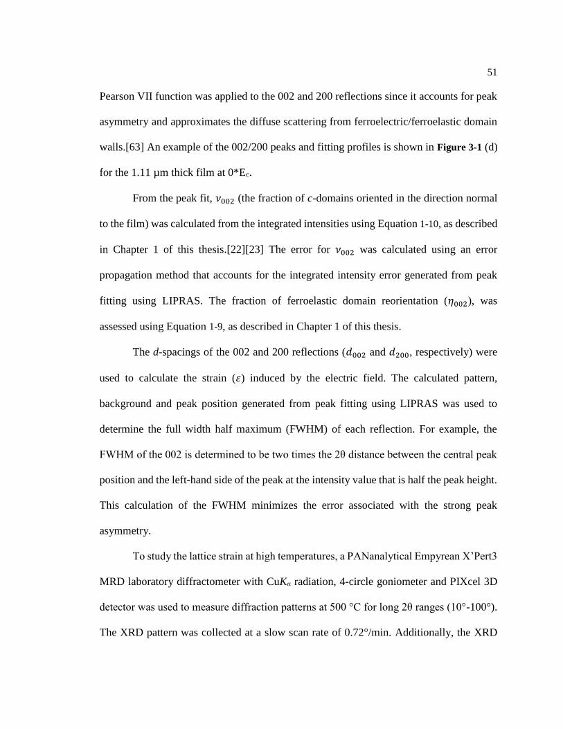
51
Pearson VII function was applied to the 002 and 200 reflections since it accounts for peak
asymmetry and approximates the diffuse scattering from ferroelectric/ferroelastic domain
walls.[63] An example of the 002/200 peaks and fitting profiles is shown in Figure 3-1 (d)
for the 1.11 µm thick film at 0*Ec.
From the peak fit, 𝜈002 (the fraction of c-domains oriented in the direction normal
to the film) was calculated from the integrated intensities using Equation 1-10, as described
in Chapter 1 of this thesis.[22][23] The error for 𝜈002 was calculated using an error
propagation method that accounts for the integrated intensity error generated from peak
fitting using LIPRAS. The fraction of ferroelastic domain reorientation (𝜂002), was
assessed using Equation 1-9, as described in Chapter 1 of this thesis.
The d-spacings of the 002 and 200 reflections (𝑑002 and 𝑑200, respectively) were
used to calculate the strain (𝜀) induced by the electric field. The calculated pattern,
background and peak position generated from peak fitting using LIPRAS was used to
determine the full width half maximum (FWHM) of each reflection. For example, the
FWHM of the 002 is determined to be two times the 2θ distance between the central peak
position and the left-hand side of the peak at the intensity value that is half the peak height.
This calculation of the FWHM minimizes the error associated with the strong peak
asymmetry.
To study the lattice strain at high temperatures, a PANanalytical Empyrean X’Pert3
MRD laboratory diffractometer with CuKα radiation, 4-circle goniometer and PIXcel 3D
detector was used to measure diffraction patterns at 500 °C for long 2θ ranges (10°-100°).
The XRD pattern was collected at a slow scan rate of 0.72°/min. Additionally, the XRD
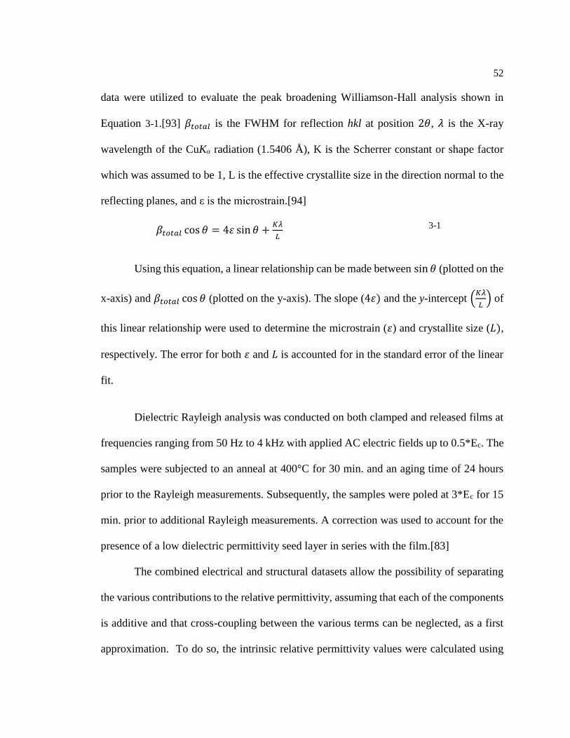
52
data were utilized to evaluate the peak broadening Williamson-Hall analysis shown in
Equation 3-1.[93] 𝛽𝑡𝑜𝑡𝑎𝑙 is the FWHM for reflection hkl at position 2𝜃, 𝜆 is the X-ray
wavelength of the CuKα radiation (1.5406 Å), K is the Scherrer constant or shape factor
which was assumed to be 1, L is the effective crystallite size in the direction normal to the
reflecting planes, and ε is the microstrain.[94]
𝛽𝑡𝑜𝑡𝑎𝑙 cos 𝜃 = 4𝜀 sin 𝜃 +𝐾𝜆
𝐿
3-1
Using this equation, a linear relationship can be made between sin 𝜃 (plotted on the
x-axis) and 𝛽𝑡𝑜𝑡𝑎𝑙 cos 𝜃 (plotted on the y-axis). The slope (4𝜀) and the y-intercept (𝐾𝜆
𝐿) of
this linear relationship were used to determine the microstrain (𝜀) and crystallite size (𝐿),
respectively. The error for both 𝜀 and 𝐿 is accounted for in the standard error of the linear
fit.
Dielectric Rayleigh analysis was conducted on both clamped and released films at
frequencies ranging from 50 Hz to 4 kHz with applied AC electric fields up to 0.5*Ec. The
samples were subjected to an anneal at 400°C for 30 min. and an aging time of 24 hours
prior to the Rayleigh measurements. Subsequently, the samples were poled at 3*Ec for 15
min. prior to additional Rayleigh measurements. A correction was used to account for the
presence of a low dielectric permittivity seed layer in series with the film.[83]
The combined electrical and structural datasets allow the possibility of separating
the various contributions to the relative permittivity, assuming that each of the components
is additive and that cross-coupling between the various terms can be neglected, as a first
approximation. To do so, the intrinsic relative permittivity values were calculated using

53
Equation 1-11 described in Chapter 1 of this thesis. The dielectric susceptibility values used
(𝜒11 and 𝜒33) are the free dielectric susceptibility (~ 230 and ~ 127 respectively),
determined by Haun et al. for bulk PZT 30/70 at 25°C.[25] It is important to note that this
calculation assumes a free system (fully released film) as opposed to the films in this study
which are either in a clamped state or 75% released state. This approximation will
overestimate the contributions from the intrinsic relative permittivity. The reversible,
extrinsic contributions to the relative permittivity were calculated from Equation 1-12, as
described in Chapter 1 of this thesis. Finally, the irreversible, extrinsic contributions to the
relative permittivity were calculated from Equation 1-13, as described in Chapter 1 of this
thesis.
3.3 Results and Discussion
3.3.1 Thickness Dependence of the Domain State
The electric field-induced change in the volume fraction of c-domains (𝜈002) is
shown in Figure 3-2 (a) for clamped, 2% Nb-doped PZT 30/70 thin films of thicknesses
0.27 µm, 0.56 µm, and 1.11 µm. Most of the clamped films underwent two electric field
cycles.

54
There are several important points to take from this figure. First, in the clamped
virgin state, 𝜈002 is thickness-dependent and ranges between 0.23 (for the 1.11 µm film)
and 0.16 (for the 0.27 µm film), which are comparable to those in the literature for similar
Figure 3-2: (a) The volume fraction of c-domains (ν002) as a function of applied electric field is shown for
2% Nb-doped PZT 30/70 thin films of thicknesses 0.27 µm, 0.56 µm, and 1.11 µm in the clamped state and
in the released state. The 75% released 1.11 µm thick film exceeded a threshold current of 1x10⁻⁴ Amps/cm2
at electric fields exceeding 2*Ec. Therefore, the data for the released 1.11 µm film above 1.5*Ec were
removed. (b) The fraction of 90° domain reorientation (η002) as a function of applied electric field is also
shown for the clamped state and the released state.

55
compositions, thicknesses and processing methods.[51][83] This thickness dependence of
𝜈002 is maintained after poling at 3*Ec. That is, thicker clamped films have a higher volume
fraction of c-domains than thinner clamped films in the initial state, during field
application, and after release of field.
The thickness dependence of 𝜈002 develops during processing of the films.[81] For
example, Figure 3-3 shows the evolution of the normalized 𝜈001 during layer-by-layer
processing of a ~0.5 µm thick sample, in which 𝜈001 increases with each additional
crystallized layer. Presumably, this evolution in the domain state is related to both the stress
state of the film upon cooling below Tc and the defect chemistry of the interfaces.
A second point of note from Figure 3-2 (a) is that upon 75% release from the
substrate (with an anneal above Tc), 𝜈002 values converge to ~0.2±0.01 for all films prior
to application of an electric field. It is proposed that after a high temperature anneal, a
Figure 3-3: The evolution of the normalized volume fraction of c-domains (ν001) during layer-by-layer
crystallization for 2% Nb-doped PZT 30/70 thin films processed via chemical solution deposition for
thicknesses ranging from ~80 nm (1 layer) to ~500 nm (6 layers).

56
redistribution of the domain state occurred. The release relieves local stress at the film-
substrate interface and reduces the bending rigidity of the structure. As a result, the released
portions of the film experienced a different stress compared to its clamped counterpart
upon cooling below Tc. Annealing above Tc allows redistribution of the domain state in the
released films; whereas, when the annealing was not performed, no change in the volume
fraction of c-domains was observed after films were released from the substrate.[28]
Thirdly, when an electric field is applied, a much larger volume fraction of c-
domains is achieved for all film thickness in released films relative to clamped ones. This
is particularly true at 3*Ec. Above 1.5*Ec, the diaphragms tear due to the high piezoelectric
strains and release geometry.[51] After tearing, portions of the film are free to deflect
vertically to relieve in-plane tensile stress, creating cantilever-like regions. This state is
referred to as global release. After global release, the 0.27 µm and 0.56 µm thick films both
show nearly 50% c-domain fractions at 3*Ec. 𝜈002 are comparable for all thicknesses even
after poling.
Figure 3-2 (b) shows electric field-induced changes in 𝜂002 for all film thickness in
the clamped state and 75% released state. In the clamped state, each film experiences
similar levels of ferroelastic domain reorientation during poling and similar back-switching
regardless of film thickness (i.e. the relaxation of reoriented domains back to a remanent
state as the electric field decreases to zero). These results suggest that substrate clamping
acts as the dominant restoring force for back switching in clamped films. 𝜂002 is ~0.18 at
3*Ec which is almost four times larger than what has been previously reported for ~1.9 µm
thick clamped 1% Mn-doped PZT 30/70 films.[51] The enhanced domain reorientation in
the 2% Nb-doped PZT films of the present study is consistent with softening of the

57
electromechanical response. Additionally, after release, all film thicknesses have
comparable electric field-induced changes in 𝜂002, as shown in Figure 3-2 (b). As expected,
more domain reorientation is observed in released films than in clamped ones.[51]
3.3.2 Thickness Dependence of Residual Stress
In the clamped state, the thinnest 0.27 µm film has the smallest out-of-plane d-
spacing for a and c-domains, 𝑑200 and 𝑑002 respectfully, as shown in Figure 3-4. The
domains present in an as-processed, clamped film are under in-plane tensile stress due to a
variety of factors including strain related to defect concentrations and thermal strain formed
due to the thermal expansion coefficient mismatch between the film and the substrate.

58
Thinner films experience a greater in-plane tensile stress that develops upon cooling
below Tc which contributes to smaller out-of-plane lattice (d) spacings for the 0.27 µm
film.[30] Additionally, since a thickness dependence in the d spacings persist above Tc, as
shown in Figure 3-5, a greater concentration of defects in thinner films also contributes to
Figure 3-4: The d-spacing for the 002 (a) and 200 reflections (b) (d002 and d200, respectively) as a function of
applied electric field increment for 2% Nb-doped PZT 30/70 thin films of thicknesses 0.27 µm, 0.38 µm,
0.56 µm, and 1.11 µm in the clamped state and the 75% released state are shown.

59
smaller d spacings for the 0.27 µm film. The d spacings were determined from the peak fit
of the 002 cubic reflection which was relatively symmetric at 500 °C. Thus, the thickness
dependence in the out-of-plane lattice spacings for clamped films is attributed to both a
larger in-plane tensile stress and a higher concentration of defects in thinner films. This
would be consistent with the data of Berfield et al. [5] suggesting that chemical solution
derived PZT films ~200 nm thick have higher in-plane tensile stresses than thicker films
when grown on Pt-coated Si substrates.
Interestingly, 𝑑200 does not monotonically increase with increasing thickness from
0.27 to 1.11 µm, shown in Figure 3-4 (b). The films reported in this study have smaller out-
of-plane lattice parameters compared to their bulk counterpart due to the in-plane tensile
stress that PZT experiences when processed on a Si substrate. If the in-plane tensile stress
decreases with increasing film thickness, as suggested elsewhere[81], it should be reflected
Figure 3-5: The thickness dependence of d-spacing for the 200 reflection (d200) for 2% Nb-doped PZT 30/70
thin films of thicknesses 0.27 µm, 0.56 µm, and 1.11 µm at room temperature (30 °C) and above the
tetragonal to cubic phase transition temperature (500 °C).

60
in a gradual increase in 𝑑200. Additionally, at elevated temperatures above Tc, d-spacing is
also observed to increase with increasing thickness for these films. However, at room
temperature, Figure 3-4 (b) shows that the 𝑑200 increases sharply as film thickness increases
from 0.27 µm to 0.38 µm, then decreases as film thickness increases further from 0.38 µm
to 1.11 µm. Reasons for this are unclear, but these changes are consistent with a reported
decrease in the reversible Rayleigh coefficient with increasing thickness for films >0.38
µm.[83] This suggests that competing factors may influence the thickness dependence of
d200.
For both clamped and released films, 𝑑002 increases with increasing applied electric
field as shown in Figure 3-4 (a). A complete data set of 𝑑002 and 𝑑200 as a function of
applied field for all film thicknesses is shown in Figure 3-6, along with those of bulk
ceramics of similar composition.[95] The field-induced changes in 𝑑002 are substantially
too large to be due only to the intrinsic piezoelectric response, as the required d33,f on
increasing field would need to exceed ~250 pm/V in the clamped films. Moreover, the 𝑑002
values do not recover when the field is removed.
61

62
Under applied electric fields, re-writing the domain state will change both the
residual stress state of the film and the domain size. For example, 𝑑002 increases with
increasing applied electric fields whereas 𝑑200 decreases. It is notable that the increase in
𝑑002 is accompanied by a reduction in the full width half maximum (FWHM) of the 002
peak, while the FWHM of the 200 peak increases on poling, as shown in Figure 3-7 (a) for
a clamped 1.11 µm thick film. This suggests that the c-domains coarsen on poling, as
shown schematically in Figure 3-8.
Figure 3-6: The d-spacing for the 002 and 200 reflections (d002 and d200, respectively) as a function of applied
electric field increment for 2% Nb-doped PZT 30/70 thin films of thicknesses (a,e) 0.27 µm, (b,f) 0.38 µm,
(c,g) 0.56 µm, and (d,h) 1.11 µm in the clamped state and the 75% released state are shown and compared to
d-spacing values for their bulk counterparts.

63
Figure 3-7: (a) The full width half maximum (FWHM) for the 002 and 200 reflections as a function of
applied electric field is plotted for 2% Nb-doped PZT 30/70 thin films of thicknesses 1.11 µm. (b) FWHM
for the 200 reflection as a function of applied electric field is plotted for clamped films of thicknesses ranging
from 0.27 µm to 1.11 µm (left); and FWHM for the 200 reflection as a function of applied electric field is
plotted for the 0.27 µm film for all release states (right).

64
As the c-domains coarsen, they begin to approach the d-spacing values for powders
of the same composition. This is presumably the cause of the irreversible strains in 𝑑002
on poling. After ferroelastic switching occurs, unswitched a-domains are placed under
further in-plane tension by neighboring c-domains reoriented by the applied electric field.
As a result, 𝑑200 decreases. This is observed for tetragonal PZT thin films as an anisotropic
electric field induced change in the out-of-plane d-spacings.[96] Additionally, the FWHM
of the a-domains increases irreversibly upon application of electric field, presumably due
to the microstrain that develops during irreversible 90° switching. Since some 90° domain
Figure 3-8: A model of the domain structure within one grain before (left) and after (right) poling to 3*Ec.
In general, the volume fraction of c-domains increases, and the c-domains coarsen upon application of electric
field.

65
reorientation is not recoverable, the residual strain associated with ferroelastic switching
results in an irreversible change in 𝑑002, 𝑑200, FWHM of 002 and FWHM of 200.
In general, the FWHM of the 200 is smaller than that of the 002, as shown in Figure
3-7 (a) for the 1.11 µm thick film (and was true for all film thicknesses). Additionally, the
FWHM of 200 increases as film thickness increases, as shown in Fig. Figure 3-7 (b).
Moreover, the thickness dependence in the FWHM of 200 is maintained even after poling.
Williamson-Hall analysis was used to determine the origin of the thickness
dependence in the FWHM of 200.[93][94] Figure 3-9 shows that both the microstrain and
crystallite size of a-domains increases as thickness increases. These values are comparable
to microstrain and crystallite sizes reported in other studies of PZT thin films grown on Si
substrates using CSD, which also report an increase in crystallite size and microstrain as
film thickness increases from 0.35 µm to 0.54 µm.[97]
Figure 3-9: The crystallite size and microstrain as a function of film thickness for 2% Nb-doped PZT 30/70
thin films in the clamped, unpoled state.

66
The increase in microstrain of a-domains with film thickness may be correlated
with the increase in 𝜈002. The local stress state of the film changes to accommodate an
increase in 𝜈002. The dependence of microstrain on domain state has also been reported for
PZT films grown in single-crystal MgO(100) substrates via puled laser deposotion.[98]
In general, the crystallite size of a-domains are at least two times as large as c-
domains. Therefore, tetragonal PZT films that are under in-plane tensile stress favor a
greater volume fraction of a-domains as well as larger a-domain crystallites, as shown
schematically in Figure 3-8. Similar to thickness-dependent trends in microstrain, the
crystallite size of a-domains increases with increasing film thickness. Therefore, the
thinnest 0.27 µm film presumably has the largest domain wall density, due to its small
crystallite size. These results suggest that the reported Rayleigh coefficiences (𝛼𝜀 and
𝜀𝑖𝑛𝑖𝑡𝑖𝑎𝑙) for the clamped, unpoled 0.27 µm film are larger relative to thicker films due in
part to the greater domain wall density present in the film.[83]
Releasing from the substrate followed by annealing above Tc (~450°C) relieves the
in-plane tensile stress of the film, resulting in an increase in d-spacing, as shown in Figure
3-4. The largest increase in both 𝑑200 and 𝑑002 occurs for the 0.27 µm film (0.76% and
1.32% increase, respectively). Upon release, the 𝑑200 and 𝑑002 converge to ~1.966±0.001
Å and ~2.015±0.01 Å, respectively, for all film thicknesses in the virgin state. The
annealing temperature is too low to expect significant changes in Pb stoichiometry, so the
change in d spacing is attributed to strain relaxation associated with the different
mechanical boundary conditions once the film is globally released. These results confirm

67
that 0.27 µm film experiences a greater strain relaxation upon release and is likely linked
to a larger increase in the irreversible Rayleigh response upon release.[83]
At applied electric fields of 3*Ec, the electric field induced increase in FWHM of
200 is enhanced post-release by ~ 9% for the 0.27 µm thick film, also shown in Figure 3-7
(b). Differences in the FWHM as a function of release state develop after globally releasing
the film from the substrate (applied electric fields ≥ 1.5*Ec for which tearing of the
diaphragms occurs). Therefore, the increase in the FWHM upon release may be due to
electric field induced non-uniformities in microstrain and/or crystallite size.
3.3.3 Rayleigh poling study
Previous studies have shown that Rayleigh parameters 𝛼𝜀 and 𝜀𝑖𝑛𝑖𝑡𝑖𝑎𝑙 have a
complicated thickness dependence that is influenced by the domain state of the film and
changes upon release.[83] Complementary Rayleigh analysis was conducted to investigate
whether the thickness dependence of 𝛼𝜀 and 𝜀𝑖𝑛𝑖𝑡𝑖𝑎𝑙 changes upon poling. Dispersion
curves of the Rayleigh parameter 𝛼𝜀 as a function of frequency are shown in Figure 3-10
for unpoled (a) and poled (b) PZT films in the clamped state. In general, 𝛼𝜀 decreases upon
poling, presumably due to the decrease in domain wall density associated with the
coarsening of c-domains inferred from the smaller FWHM of the 002 reflection. Small (<
9%) thickness independent changes in 𝛼𝜀 occur upon poling for clamped films.

68
Upon 75% release from the substrate, 𝛼𝜀 increases for all film thickness, as shown
in Figure 3-10 (c). Moreover, after poling, the change in 𝛼𝜀 for the 75% released film is
more than double that for the clamped film. The changes in 𝛼𝜀 are the largest at low
frequencies, confirming observations reported elsewhere that substrate clamping has a
greater influence on slower, irreversibly moving, domain walls.[83] Finally, since releasing
the film from the substrate enhances ferroelastic domain reorientation, it can be assumed
Figure 3-10: Frequency dispersion of the Rayleigh parameter αε as a function of film thickness ranging from
0.27 µm to 1.11 µm for 2% Nb-doped PZT 30/70 thin films in the clamped state for unpoled (a) and poled
(b) films, as well as in the 75% released state for unpoled (c) and poled (d) films.

69
that the greater change in 𝛼𝜀 for released films is due to a greater decrease in domain wall
density resulting from c-domain coarsening upon poling.
Dispersion curves of 𝜀𝑖𝑛𝑖𝑡𝑖𝑎𝑙 are shown in Figure 3-11 for unpoled (a) and poled (b)
clamped PZT films. 𝜀𝑖𝑛𝑖𝑡𝑖𝑎𝑙 decreases upon poling due to the increases in volume fraction
of c-domains coupled with a decrease in domain wall density due to coarsening of the c-
domains. The thickness dependence of 𝜀𝑖𝑛𝑖𝑡𝑖𝑎𝑙 is increases after poling, with a three times
larger change in 𝜀𝑖𝑛𝑖𝑡𝑖𝑎𝑙 for the 1.11 µm film (~16%) compared to the 0.27 µm film (~5%).
This thickness-dependent change in 𝜀𝑖𝑛𝑖𝑡𝑖𝑎𝑙 is not due to differences in the ferroelastic
domain reorientation, since 𝜂002 is not thickness-dependent (see in Figure 3-2).
Additionally, the thickness-dependent change in 𝜀𝑖𝑛𝑖𝑡𝑖𝑎𝑙 is not intrinsically driven since
there is no change in the thickness dependence of 𝜈002.

70
Phenomenology can be used to determine whether thickness-dependent changes in
𝜀𝑖𝑛𝑖𝑡𝑖𝑎𝑙 upon release and after poling is driven by intrinsic or reversible extrinsic
contributions to the permittivity. Estimated values for 𝜀𝑟,𝑖𝑛𝑡𝑟𝑖𝑛𝑠𝑖𝑐 are plotted as a function
of film thickness for unpoled films in both the clamped and 75% released states, as shown
in the lower portion of Figure 3-12 (a). For a clamped unpoled film, 𝜀𝑟,𝑖𝑛𝑡𝑟𝑖𝑛𝑠𝑖𝑐 decreases
as thickness increases, as expected based on the thickness-dependence of 𝜈002. However,
Figure 3-11: Frequency dispersion of the Rayleigh parameter εinitial as a function of film thickness ranging
from 0.27 µm to 1.11 µm for 2% Nb-doped PZT 30/70 thin films in the clamped state for unpoled (a) and
poled (b) films, as well as in the 75% released state for unpoled (c) and poled (d) films.

71
upon 75% release from the substrate, the thickness dependence in 𝜀𝑟,𝑖𝑛𝑡𝑟𝑖𝑛𝑠𝑖𝑐 is reduced.
Therefore, the thickness dependence in 𝜀𝑖𝑛𝑖𝑡𝑖𝑎𝑙 for the unpoled, 75% released state is due
predominantly to a thickness dependence in the reversible extrinsic contribution to the
relative permittivity (𝜀𝑟,𝑒𝑥𝑡𝑟𝑖𝑛𝑠𝑖𝑐𝑟𝑒𝑣𝑒𝑟𝑠𝑖𝑏𝑙𝑒 ). Upon release, 𝜀𝑖𝑛𝑖𝑡𝑖𝑎𝑙 decreases by ~6% for all film
thicknesses, as shown in Figure 3-11 (c), which is mainly related to a shift from reversible
to irreversible domain wall contributions to the relative permittivity.[83]
Phenomenological calculations suggest that the 𝜀𝑟,𝑒𝑥𝑡𝑟𝑖𝑛𝑠𝑖𝑐𝑟𝑒𝑣𝑒𝑟𝑠𝑖𝑏𝑙𝑒 decreases upon release for all
film thicknesses, driving the overall decrease in 𝜀𝑖𝑛𝑖𝑡𝑖𝑎𝑙.
For clamped films, 𝜀𝑟,𝑖𝑛𝑡𝑟𝑖𝑛𝑠𝑖𝑐 decreases upon poling, with a comparable decrease
for all film thicknesses (3.4% decrease for 0.27 µm vs. 4.0% decrease for 1.11 µm), as
shown in the lower portion of Figure 3-12 (b). Therefore, it is confirmed that the thickness-
dependent change in 𝜀𝑖𝑛𝑖𝑡𝑖𝑎𝑙 upon poling for a clamped film is not due to intrinsic changes.
In general, 𝜀𝑟,𝑒𝑥𝑡𝑟𝑖𝑛𝑠𝑖𝑐𝑟𝑒𝑣𝑒𝑟𝑠𝑖𝑏𝑙𝑒 decreases as thickness increases regardless of the release state for
Figure 3-12: The intrinsic (εr,intrinsic) and reversible, extrinsic (εr,extrinsic) contributions to the permittivity as a
function of film thickness ranging from 0.27 µm to 1.11 µm for 2% Nb-doped PZT 30/70 thin films in the
clamped and 75% released state for unpoled (a), as well as in the clamped state for unpoled and poled films
(b).

72
both unpoled and poled samples, as shown in the upper portion of Figure 3-12 (a) and (b).
These results suggest that substrate clamping creates deep potential wells in the potential
energy landscape in which reversible motion of domain walls is preferred, consistent with
studies by Griggio et al.[54] Additionally, it is probable that domain wall motion in thinner
films exhibit more reversible motion compared to thicker films, since a greater fraction of
domain walls in thinner films are subject to clamping effects at the film-substrate interface.
For clamped films, the decrease in 𝜀𝑟,𝑒𝑥𝑡𝑟𝑖𝑛𝑠𝑖𝑐𝑟𝑒𝑣𝑒𝑟𝑠𝑖𝑏𝑙𝑒 upon poling in the thicker 1.11 µm film is
double that for the thinner 0.27 µm film (20% decrease vs. 10% decrease, respectively).
Therefore, the thickness-dependent change in 𝜀𝑖𝑛𝑖𝑡𝑖𝑎𝑙 upon poling for a clamped film is
primarily due to extrinsic contributions. It is proposed that thicker films, which have
reduced in-plane tensile stress and defect concentrations, experience a greater coarsening
of c-domains upon poling. As a result, thicker films have smaller domain wall densities in
the poled state, resulting in a greater decrease in both 𝜀𝑟,𝑒𝑥𝑡𝑟𝑖𝑛𝑠𝑖𝑐𝑟𝑒𝑣𝑒𝑟𝑠𝑖𝑏𝑙𝑒 and 𝜀𝑖𝑛𝑖𝑡𝑖𝑎𝑙 upon poling.
The relative permittivity can be separated into three contributions: intrinsic,
reversible extrinsic and irreversible extrinsic contributions, as shown in Figure 3-13. It was
found that for these films, 𝜀𝑟,𝑒𝑥𝑡𝑟𝑖𝑛𝑠𝑖𝑐𝑟𝑒𝑣𝑒𝑟𝑠𝑖𝑏𝑙𝑒 makes up a majority of the relative permittivity (at
least 70%). Therefore, the thickness dependence in 𝜀𝑟,𝑒𝑥𝑡𝑟𝑖𝑛𝑠𝑖𝑐𝑟𝑒𝑣𝑒𝑟𝑠𝑖𝑏𝑙𝑒 will dictate the thickness
dependence of the overall relative permittivity. As noted above, the extraction of the three
contributions to the relative permittivity assumes that the contributions can be stacked
linearly. However, the intrinsic and extrinsic contributions may be inter-related. In this
case, we assume that the cross terms are negligible at low applied electric fields (within the
Rayleigh regime: 𝐸𝑎𝑝𝑝𝑙𝑖𝑒𝑑 ≤ 𝐸𝑐). It is also possible that properly accounting for clamping

73
of the intrinsic relative permittivity would drop that contribution by roughly a factor of
two, with the difference contributing to the reversible extrinsic permittivity.
3.4 Conclusions
In situ high resolution XRD was used to investigate the influence that substrate
clamping and residual stress have on the thickness dependence of the volume fraction of
c-domains and electric field induced strain upon release. Tetragonal {001}
Pb0.99(Zr0.3Ti0.7)0.98Nb0.02O3 films were deposited using CSD with thicknesses ranging from
Figure 3-13: The intrinsic (εr,intrinsic), reversible and irreversible extrinsic (εr,extrinsic) contributions to the
permittivity as a function of film thickness ranging from 0.27 µm to 1.11 µm for 2% Nb-doped PZT 30/70
thin films in the clamped state for unpoled (a) and poled films (b), as well as in the 75% released state for
unpoled (c) and poled films (d).

74
0.27 µm to 1.11 µm. The thickness dependence of 𝜈002 is influenced by the concentration
of defects in the films and the degree of residual stress formed upon cooling below Tc. This
thickness dependence persists after poling and is alleviated upon release. The thickness
dependence of 𝜈002 can result in differences in the intrinsic contributions to reversible
Rayleigh parameter, 𝜀𝑖𝑛𝑖𝑡𝑖𝑎𝑙. The thinnest 0.27 µm film has the smallest d-spacings for both
a and c-domains due to a greater in-plane tensile stress and a higher concentration of
defects present in thinner films. In general, the electric field produced changes in d002 and
d200 associated with irreversible coarsening of c-domains as well as irreversible 90° domain
reorientation, both of which will change the local stress state of the film. The thickness
dependence of the FWHM of 002 is due to increasing microstrain and crystallite size with
film thickness. Releasing the film from the substrate relieves residual stress, increases the
FWHM of the 200 reflection and enhances ferroelastic domain reorientation. Residual
stress in a film indirectly affects the extent of reversible, extrinsic contributions to the
relative permittivity. These results confirm that residual stress at the film-substrate
interface creates a potential energy landscape with deep potential wells, such that reversible
motion of domain walls is preferred.

75
Chapter: 4 Influence of Elastic Layer Thickness on Mechanical
and Ferroelastic Behavior of PiezoMEMS Beams
4.1 Introduction
Pb(ZrxTi1-x)O3 (PZT) thin films serve as the active layer in piezoelectric
microelectromechanical systems (piezoMEMS) for applications such as mass sensors,
radio frequency (RF) switches, transformers, micromachined ultrasound transducers, and
small-scale robotic actuators.[3][4][5][6][7][8][9][10][11][12] For these applications,
released structures, such as a cantilever or fixed-fixed beam geometry, enhance the out-of-
plane deflection for actuators and in-plane stresses for sensors. A typical piezoMEMS
structure consists of a Pt/PZT/Pt/TiO2/SiO2 stack grown on a Si substrate, although many
options for the electrodes (Pt, IrO2, etc.) and the passive elastic layer (here SiO2) are
possible. The elastic layer thickness and its stress state can be tailored to control the static
deformation of the piezoelectric layer, rigidity, resonant frequency and the drive voltage
required to reach a particular deflection.[3][4][99][100][101]
The residual stress of each layer (𝜎𝑖) can be approximated as an uniaxial residual
stress field using the polynomial in Equation 4-1 where h is the thickness of the individual
layer and z is the z-position across the layer thickness from the film’s midplane.[102]
𝜎𝑖 = ∑ 𝜎𝑘 ∗ (2𝑧
ℎ)
𝑘∞𝑘=0 where 𝑧 ∈ (
−ℎ
2,
+ℎ
2)
4-1
Therefore, for the first order approximation, the first term (𝜎0) represents the mean
stress of the layer, and the second term (𝜎1 ∗ (2𝑧
ℎ)) represents the linear stress gradient in
the film resulting from growth stresses. For a multilayered system, the mean residual stress

76
can be represented by the integrated stress, the residual stresses (𝜎𝑖) multiplied by the
thickness (𝑡𝑖) of each layer, as shown in Equation 4-2.[103]
𝜎1,2,…𝑛 =∑ 𝜎𝑖∗𝑡𝑖
𝑛𝑖
∑ 𝑡𝑖𝑛𝑖
4-2
The residual stress that develops during processing includes both thermal and
growth stresses. Thermal stress develops due to the mismatch in the coefficient of thermal
expansion (𝛼𝐶𝑇𝐸) between the film and the substrate. Typically, on a blanket Si substrate,
a crystallized PZT layer is under biaxial, in-plane tension since 𝛼𝐶𝑇𝐸 of Si (2.6 ppm/°C) is
less than that of PZT in the paraelectric phase (6.7-9.4 ppm/°C, depending on
composition).[75] Additionally, the thermal SiO2 layer is under compression, both due to
intrinsic growth stresses and since 𝛼𝐶𝑇𝐸 of Si is greater than that of SiO2 (0.5 ppm/°C).[104]
Intrinsic stresses can vary during layer-by-layer processing involving repetitive
high temperature annealing steps, such as during chemical solution deposition
(CSD).[30][81][82] In particular, either line defects or non-stoichiometric defects vary in
concentration across a film thickness, resulting in an out-of-plane stress gradient as a
function of film depth. For example, during CSD of PZT thin films, Pb loss to the film-
substrate interface and Zr/Ti segregation are common occurrences.[71][105][106]
Therefore, intrinsic stress as well as thermal stress may be present in the PZT, contributing
to the overall residual stress in the PiezoMEMS device stack (𝜎𝑠𝑡𝑎𝑐𝑘).
In order to relieve 𝜎𝑠𝑡𝑎𝑐𝑘, a cantilever changes length in response to the mean stress
and bends to relieve stress gradients.[102] The overall deflection can be modeled using
Stoney’s equation for cantilevers that have aspect ratios 𝐿
𝑏≥ 3, where L is the length of the

77
cantilever and b is the width of the cantilever.[107] Additionally, finite element analysis
(FEA), Bernoulli-Euler beam bending and other analytical methods have been proposed to
describe the deflection of cantilevers and fixed-fixed beams.
[99][107][108][109][110][111]
The passive layer (typically SiO2) in PiezoMEMS is used to amplify deflection,
while providing desired levels of stiffness to control resonance frequencies. The
differences in the residual stress states between the tensile PZT layer and the compressive
SiO2 layer amplifies the static deflection of a cantilever tip since the layers are typically
located on opposite sides of the neutral axis (�̅�).[99][110][112] The neutral axis can be
calculated using Equation 4-3, in which 𝑡𝑖 is the thickness, 𝐸𝑖 is the Young’s modulus of a
given layer, 𝐸𝑃𝑍𝑇 is the Young’s modulus of PZT and 𝑦𝑖 is the centroid of a given layer.
�̅� =∑[𝑡𝑖∗(
𝐸𝑖𝐸𝑃𝑍𝑇
)∗𝑦𝑖]
∑[𝑡𝑖∗(𝐸𝑖
𝐸𝑃𝑍𝑇)]
4-3
The added thickness of the SiO2 layer increases the flexural rigidity (D) and bending
stiffness (S) of the device, as shown in Equation 4-4, where E is the Yong’s modulus, t is
the overall thickness and ν is the Poison’s ratio of the device.[113]
𝐷 =𝐸∗𝑡3
12∗(1−𝜈2)=
𝑆
(1−𝜈2)
4-4
D and t are important design parameters for tuning the fundamental resonance
frequency (𝑓0) for many PiezoMEMS devices, as shown in Equation 4-5, where 𝜌 is the
density. 𝛾 is a constant related to the length (L) of the structure and scaled frequency
parameter or eigenvalue (k), as shown in Equation 4-6.[114]

78
𝑓0 = 𝛾2√𝐷
𝜌∗𝑡
4-5
𝛾 =√𝑡∗𝑘
𝐿
4-6
The normalized beam rigidity depends on the thickness of
structures.[110][111][115][116] If 𝐸𝑆𝑖𝑂2> 𝐸𝑃𝑍𝑇 then the average 𝐸𝑠𝑡𝑎𝑐𝑘 increases, which
will increase D and S. However, it is difficult to determine whether SiO2 or PZT has the
larger Young’s modulus since the reported values for 𝐸𝑆𝑖𝑂2 vary from 60 GPa to 80 GPa
[117][118] and 𝐸𝑃𝑍𝑇 varies from 40 GPa to 100 GPa with texture, composition, doping,
etc.[119]
In the case of a fixed-fixed beam geometry, more complicated buckling patterns
can occur in thinner devices. As the thickness of the SiO2 layer decreases, 𝑓0 is expected
to decrease. However, 𝑓0 will increase as the buckling complexity increases.[120]
Therefore, for a fixed-fixed beam geometry, there may be competing mechanisms, flexural
rigidity vs. buckling mode shape, that dictate the shift in resonance frequency as the
thickness of the SiO2 layer is varied.
As the rigidity of the device increases, at some point the ferroelastic response of
the PZT layer will be suppressed, in the same way that substrate rigidity suppresses the
ferroelastic response in blanket films.[51][86] The influence of substrate clamping on the
dielectric properties of PZT can be investigated using Rayleigh analysis.[54][83]
Therefore, this technique can be utilized to determine how the dielectric properties of the
PZT layer change as the rigidity of the device increases, i.e. the thickness of the SiO2 layer
increases. The Rayleigh law is described using Equation 1-8 in Chapter 1 of this thesis. In

79
short, 𝜀𝑖𝑛𝑖𝑡𝑖𝑎𝑙, is the reversible dielectric Rayleigh coefficient which contains both the
reversible extrinsic and intrinsic contributions to the permittivity. 𝛼𝜀, is the irreversible
dielectric Rayleigh coefficient associated with extrinsic contributions to the permittivity
from irreversible movement of domain walls and phase boundaries through a random
potential energy landscape.[21]
Griggio et al. has shown that polycrystalline Pb(Zr0.52Ti0.48)O3 (PZT 52/48) films
that are released from the substrate have enhanced 𝛼𝜀 and 𝜀𝑖𝑛𝑖𝑡𝑖𝑎𝑙.[54] Conversely, Denis
et al. reported that 𝛼𝜀 increases, while 𝜀𝑖𝑛𝑖𝑡𝑖𝑎𝑙 decreases, with increasing release state for
{001} textured PZT 30/70 films of thickness ranging from 0.27 µm to 1.11 µm. It is
suggested that there is a shift of at least some domain walls from reversible to irreversible
motion upon release.[83] Therefore, it is important to understand how the elastic layer
thickness (i.e. device rigidity) influences the irreversible or reversible contributions to the
relative permittivity of the PZT layer. This will ultimately govern device performance.
4.2 Fabrication
Tetragonal, {001} textured Pb(Zr0.3Ti0.70)O3 (PZT 30/70) based PiezoMEMS
actuators were fabricated on a (001) silicon wafer in a cantilever and fixed-fixed beam
geometry. The free-standing composite stack is comprised of either a 0.76 µm or 2.035 µm
thick SiO2 elastic layer, followed by a TiO2 adhesion layer, a Pt bottom electrode, a PbTiO3
seed layer, a PZT 30/70 active layer, and an IrO2 top electrode layer. A schematic of the
device stack, including the thicknesses of each layer and lateral dimensions, is shown in
Figure 4-1 for the fixed-fixed beam geometry (a, b) and the cantilever geometry (c, d). SEM
images of the side view of both devices are also included.

80
The devices were fabricated at the US Army Research Laboratory (ARL). Full
details of the processing are described elsewhere.[99][121] In summary, thermal SiO2 was
grown by annealing a Si wafer at 700 °C. The thickness of the SiO2 layer was chosen such
that either a positive or negative tip displacement of the cantilever was achieved based on
a linear residual stress deformation model (2.035 µm or 0.76 µm thick SiO2,
respectively).[99] Next, a layer of Ti was sputtered and oxidized at 750 °C in flowing
Figure 4-1: A schematic illustrating the dimensions and film stack of the fixed-fixed beams, including a top
down view of the patterned features (a) and side view of the device stack (b) with a SEM image of the device
with a 2.035 µm SiO2 elastic layer. Also shown is a schematic listing of the dimensions and film stack for
cantilevers of lengths ranging from 250 µm to 50 µm, including a top down view of the patterned features
(c) and side view of the device stack (d) with a SEM image of cantilevers with a 2.035 µm SiO2 elastic layer.

81
oxygen to form the adhesion/diffusion barrier layer. The Pt bottom electrode was deposited
onto the adhesion layer at 500 °C using magnetron sputtering. A PbTiO3 seed layer was
deposited via a 2-Methoxyethanol (2-MOE) based CSD process described
elsewhere.[58][122] The seed layer promoted the growth of the {001} textured PZT film;
the PZT films were also grown via 2-MOE based CSD with 12% excess lead. The PZT
films were spun, pyrolyzed and crystallized at 700 °C repeatedly until a ~0.5 µm thick film
was achieved. Details of the CSD process used for the PZT film is described
elsewhere.[121] Finally, IrO2 was sputtered onto the PZT layer to act as the top electrode,
instead of Pt, to improve capacitor reliability.[123]
The cantilever and fixed-fixed beam geometries were achieved via a four-mask
photopatterning and release process described elsewhere.[99][121] Argon ion milling was
used to remove regions of the IrO2/PZT/PbTiO3/Pt/TiO2/SiO2 stack to expose the
underlying silicon substrate and create the release trench. An isotropic XeF2 etch was then
used to remove parts of the Si substrate underneath the device stack, creating the free-
standing structures. For the cantilever actuator, the IrO2/PZT/PbTiO3/Pt/TiO2/SiO2 stack
extends the full length of the cantilever beam. However, for the fixed-fixed beam structure,
the IrO2/PZT/PbTiO3/Pt/TiO2/SiO2 stack is only present 250 µm along the length of the
beam from the clamped edges on either side of the bridge structure, as shown in the cross-
sectional schematic of Figure 4-1 (a). Only SiO2 is present at the center of the bridge
structure; this is shown in navy blue in Figure 4-1 (a) (500 µm in length).

82
4.3 Modeling
FEA (via COMSOL Multiphysics® software[124]) was used to model the vertical
deflection of a 2-dimensional (2-D) cantilever 250 µm in length, 30 µm in width using the
material properties listed in Table 4-1. All layers were assumed to behave as linear elastic
materials with isotropic properties. Since PbTiO3 shares similar material properties to PZT
and the thickness of the PbTiO3 is an order of magnitude less than that of PZT, the PbTiO3
layer was included as part of the PZT layer in the modeling for simplicity. Since 𝐸𝑃𝑍𝑇 can
vary with composition, dopant type and texture, 𝐸𝑃𝑍𝑇 values ranging from 40 GPa to 100
GPa were tested in the simulation, which is representative of the range of 𝐸𝑃𝑍𝑇 found in
the literature.[119]
The residual stress of the PZT and SiO2 layers were based on thermal stress
calculations for a film grown on a 0.5 mm thick Si substrate (𝐸𝑆𝑖 = 160 GPa [130], 𝜈𝑆𝑖 =
0.17 [130] and 𝛼𝐶𝑇𝐸,𝑆𝑖 = 2.6 ppm/°C [131][132]) using classical laminate theory.[133] A
range of values for 𝜎𝑃𝑍𝑇 and 𝜎𝑆𝑖𝑂2 were chosen to account for the variations in 𝛼𝐶𝑇𝐸 of PZT
[134] and SiO2 [135] reported in the literature. 𝜎𝑃𝑍𝑇 was varied between 0 MPa and 300
MPa, corresponding to a 𝛼𝐶𝑇𝐸,𝑃𝑍𝑇 range of 2 ppm/°C to 6 ppm/°C, respectively, for 𝐸𝑃𝑍𝑇 =
Table 4-1: Film Thickness and Material Properties of Device Layers
Material Thickness (µm) Young’s Modulus (GPa) Poisson’s Ratio Initial Stress (MPa)
IrO2 0.1 262 [123] 0.3 [123] -900 [125]
PZT 0.5 40 to 100 [119][126] 0.3 [81] 0 to 300
Pt 0.1 182 [127] 0.41 [127] 700 [99]
TiO2 0.035 250 [128] 0.27 [128] 500 [129]
SiO2 2.035 or 0.76 60 to 100 [117][126] 0.17 [117] 0 to -125

83
80 𝐺𝑃𝑎. 𝜎𝑆𝑖𝑂2 was varied between 0 GPa and -125 GPa, corresponding to a 𝛼𝐶𝑇𝐸,𝑆𝑖𝑂2
range
of 2.5 ppm/°C to 0.25 ppm/°C, respectively, for 𝐸𝑆𝑖𝑂2= 70 𝐺𝑃𝑎.
4.4 Characterization
The cantilever tip displacements were measured using optical profilometry (Zygo
NexviewTM NX2, 3D Optical Surface Profiler), typically in a CSI measurement mode, high
Z resolution, high dynamic range, 10x magnification, 1x or 0.5x zoom depending on
feature size, and 100 µm z-scan length to view both the device features and etch pit
underneath. The measured tip displacements were used as a reference point for the
COMSOL simulations. Based on this reference, the residual stress combinations for PZT
and SiO2 that give the desired tip displacement were identified. The vertical deflections
and buckling nature of the fixed-fixed beams were also measured using optical
profilometry.
Polarization vs. electric field (P–E) hysteresis loops were measured at a frequency
of 10 Hz using a Radiant Precision Ferroelectric Tester for cantilever and fixed-fixed
beams with SiO2 layers of thickness 2.035 µm and 0.76 µm. Rayleigh analysis was also
conducted. The dielectric properties were measured at frequencies ranging from 100 Hz to
4 kHz with applied AC electric fields up to 0.5*Ec (Ec = 55 ± 5 kV/cm) after the samples
were annealed (open circuit) at ~450°C for 30 min. and aged for 24 hours.

84
4.5 Results and Discussion
4.5.1 Influence of Stress and Thickness on Cantilever Tip Deflection
Optical profilometry measurements for cantilevers of varying lengths are shown in
the inset of Figure 4-2. For the longest cantilever (i.e. L=250 µm), the tip deflection is
positive for cantilevers with a 2.035 µm thick SiO2 layer and negative for cantilevers with
a 0.76 µm thick SiO2 layer. Sample tilting was accounted for by subtracting the tilt
measured from clamped regions of the sample from the overall tip deflection within the
area of interest. The magnitude of tip deflection is greater for the 0.76 µm thick SiO2 device
compared to the 2.035 µm thick SiO2 device (-26.0 µm and +18.3 µm, respectively, when
L=250 µm), as expected based on the lower rigidity. Additionally, as L decreases, the
magnitude of the tip deflection also decreases regardless of SiO2 thickness, as shown in the
SEM image of Figure 4-1 (d).
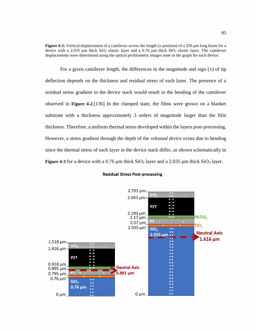
85
For a given cantilever length, the differences in the magnitude and sign (±) of tip
deflection depends on the thickness and residual stress of each layer. The presence of a
residual stress gradient in the device stack would result in the bending of the cantilever
observed in Figure 4-2.[136] In the clamped state, the films were grown on a blanket
substrate with a thickness approximately 3 orders of magnitude larger than the film
thickness. Therefore, a uniform thermal stress developed within the layers post-processing.
However, a stress gradient through the depth of the released device exists due to bending
since the thermal stress of each layer in the device stack differ, as shown schematically in
Figure 4-3 for a device with a 0.76 µm thick SiO2 layer and a 2.035 µm thick SiO2 layer.
Figure 4-2: Vertical displacement of a cantilever across the length (x-position) of a 250 µm long beam for a
device with a 2.035 µm thick SiO2 elastic layer and a 0.76 µm thick SiO2 elastic layer. The cantilever
displacements were determined using the optical profilometry images inset in the graph for each device.

86
Cantilever bending alleviates the residual stresses in the device, more so in layers
located farther from the neutral axis. The position of the neutral axis changes as the
thickness of the SiO2 changes, as shown in Figure 4-3. Cantilevers with a 0.76 µm thick
SiO2 layer exhibits a negative vertical deflection, suggesting that the region above the
neutral axis was under compression and/or the region below the neutral axis was under
tension post-processing. For a device with a 0.76 µm thick SiO2 layer, the neutral axis
(Equation 4-3) lies within the Pt bottom electrode. The layers located above the neutral axis
in this device include the PbTiO3 seed layer, the PZT active layer and the IrO2 top electrode.
Since PbTiO3 and PZT develop in-plane tensile stress when processed on a Si substrate, it
is unlikely that the alleviation of the residual thermal stress of these layers will result in the
downward cantilever tip bending in this device. The IrO2 top electrode is under
compression post-processing, with a large 𝜎𝐼𝑟𝑂2of -913 MPa [125], which contributes
strongly to the overall deflection of this device. The influence of the residual stress of the
IrO2 top electrode may be greater for the thinner device since the top electrode (0.1 µm)
makes up a greater volume of the device stack. If we assume 𝜎𝑆𝑖𝑂2= -75 MPa and 𝜎𝑃𝑍𝑇=
100 MPa, the average residual stress above the neutral axis is compressive and ~2x larger
in magnitude than that below the neutral axis, (-69 MPa vs. 34 MPa for above and below
the neutral axis, respectively, calculated using Equation 4-2). Therefore, upon release, the
cantilever deflected in the negative vertical direction, presumably, to alleviate the in-plane
stress in the top electrode.
Figure 4-3: A cross-sectional schematic of the thermal residual stress that develops post-processing for a
multilayered device, with a 0.76 µm thick SiO2 layer and a 2.035 µm thick SiO2 layer, processed on a Si
substrate. The z-position of the neutral axis is shown for each device.

87
Cantilevers with a 2.035 µm thick SiO2 layer exhibit a positive vertical deflection,
suggesting that the influence of 𝜎𝐼𝑟𝑂2 on the tip deflection decreases as the thickness of the
SiO2 layer increases. For a device with a 2.035 µm thick SiO2 layer, the neutral axis lies in
the SiO2 layer. As a result, the variation in residual stresses above the neutral axis is greater
for this device, since this region includes layers in compression (IrO2 top electrode and
~0.4 µm of SiO2) and layers in tension (PZT, PbTiO3, Pt and TiO2). If we assume 𝜎𝑆𝑖𝑂2= -
75 MPa and 𝜎𝑃𝑍𝑇= 100 MPa, the average residual stress below the neutral axis is
compressive and more than 6x larger in magnitude than that above the neutral axis, (-75
MPa vs. 12 MPa for below and above the neutral axis, respectively, calculated using
Equation 2).
4.5.2 FEA Modeling of Cantilever Tip Deflection
Using COMSOL Multiphysics® software, FEA models of the device stack after
release were created to determine the residual stress in each layer in order to match the
observed tip displacement. Figure 4-4 shows the mesh used for these simulations. Figure
4-5 shows a 2-D model of the cantilever tip displacement and a cross-section illustrating
the in-plane residual stresses for each layer for cantilevers with either a 2.035 µm thick or
0.76 µm thick SiO2 layer. Post-deflection, stress gradients form in regions of the device
that are far from the neutral axis, as seen in the 2.035 µm thick SiO2 layer and 0.5 µm PZT
layer in the 2.035 µm SiO2 device. COMSOL was also used to determine which
combinations of 𝜎𝑃𝑍𝑇 and 𝜎𝑆𝑖𝑂2 produced the experimental tip deflection for both the 2.035
µm and 0.76 µm thick SiO2 cantilevers. The absolute value of the residual stress ratio of
PZT to SiO2 (𝜎𝑃𝑍𝑇
𝜎𝑆𝑖𝑂2
) decreases as 𝐸𝑃𝑍𝑇 decreases, regardless of SiO2 thickness or 𝐸𝑆𝑖𝑂2, as

88
shown in Figure 4-6 (a). For a given 𝐸𝑃𝑍𝑇, there is a ~ 4% difference in 𝜎𝑃𝑍𝑇
𝜎𝑆𝑖𝑂2
between the
2.035 µm and 0.76 µm thick SiO2 device if 𝐸𝑆𝑖𝑂2= 60 GPa. As 𝐸𝑆𝑖𝑂2
increases, the linear
relationship (𝐸𝑃𝑍𝑇 vs. 𝜎𝑃𝑍𝑇
𝜎𝑆𝑖𝑂2
) for the 2.035 µm thick SiO2 device converges with that for
the 0.76 µm thick SiO2 device. As SiO2 becomes less compliant (greater 𝐸𝑆𝑖𝑂2), a greater
residual stress may form in the SiO2 layer and dictate 𝜎𝑃𝑍𝑇
𝜎𝑆𝑖𝑂2
regardless of SiO2 thickness.
However, it is unlikely that 𝐸𝑆𝑖𝑂2> 70 GPa.[117][118] Therefore, this suggests that 𝜎𝑆𝑖𝑂2
may be thickness dependent, resulting in differences in 𝜎𝑃𝑍𝑇
𝜎𝑆𝑖𝑂2
with SiO2 thickness. A
thickness dependence in 𝜎𝑆𝑖𝑂2 is not uncommon and may be related to variations in
processing.[99]
Figure 4-4: The mesh used for FEA simulations of the multilayered PiezoMEMS device.

89
Figure 4-5: A 2-D COMSOL model of the tip deflection of a 250 µm long cantilever, and a schematic cross-
section showing the residual stress in each layer after deflection for a device with a 2.035 µm thick SiO2
elastic layer and a 0.76 µm thick SiO2 elastic layer.

90
Figure 4-6: (a) The linear relationship between the residual stress ratio (σPZT/σSiO2) and the PZT Young’s
Modulus (EPZT) plotted for a device with a 2.035 µm thick SiO2 elastic layer and a 0.76 µm thick SiO2 elastic
layer. The comparison is shown for two different SiO2 Young’s Modulus (ESiO2): 60 GPa and 100 GPa.
Contour plots of σPZT vs. σSiO2 for a variety of cantilever tip displacements for a device with a 2.035 µm thick
SiO2 elastic layer (b, d) and a 0.76 µm thick SiO2 elastic layer (c, e) for 𝜎𝐼𝑟𝑂2 for 900 MPa and 1100 MPa.

91
Contour plots of 𝜎𝑃𝑍𝑇 vs. 𝜎𝑆𝑖𝑂2 for a variety of tip displacements is also shown in
Figure 4-6 for the 2.035 µm (b, d) and 0.76 µm (c, e) thick SiO2 devices with 𝐸𝑃𝑍𝑇 = 80
GPa and 𝐸𝑆𝑖𝑂2= 60 GPa. The values of 𝜎𝑃𝑍𝑇 and 𝜎𝑆𝑖𝑂2
are not the values of residual stress
measured in the PZT and SiO2 layers of the devices in this study. Rather, the FEA model
represents a general (but complex) relationship between the layer thickness, residual stress,
elastic modulus and tip displacement of a cantilever device. The grey diagonal lines on the
contour plots represent a possible tip displacement (µm) and combinations of 𝜎𝑃𝑍𝑇 and
𝜎𝑆𝑖𝑂2 to achieve that displacement. The slope of the line is
𝜎𝑃𝑍𝑇
𝜎𝑆𝑖𝑂2
. The contour plots can be
used to determine the range of 𝜎𝑆𝑖𝑂2 that will produce the appropriate tip displacement if
𝜎𝑃𝑍𝑇 ranges from 50 to 150 MPa, as shown in the white shaded regions. The offset of the
line (𝑍𝑜𝑓𝑓𝑠𝑒𝑡) corresponds to the tip displacement at zero residual stress of PZT and SiO2
(𝜎𝑃𝑍𝑇 = 𝜎𝑆𝑖𝑂2= 0 GPa) and depends on the residual stress of the IrO2 top electrode (𝜎𝐼𝑟𝑂2
).
For a given film thickness (2.035 µm SiO2), the range of 𝜎𝑆𝑖𝑂2 that will produce the
appropriate tip displacement varies significantly with 𝜎𝐼𝑟𝑂2, as shown in Figure 4-6 for
𝜎𝐼𝑟𝑂2= -900 MPa (b) and 𝜎𝐼𝑟𝑂2
= -1100 MPa (d). Changing the 𝜎𝐼𝑟𝑂2 will shift the origin
of the contour plot, thereby shifting the linear relationship between 𝜎𝑆𝑖𝑂2 and 𝜎𝑃𝑍𝑇 for the
desired tip displacement (white line). To obtain a self-consistent combination of 𝜎𝑃𝑍𝑇 and
𝜎𝑆𝑖𝑂2 that will yield the desired tip displacement in each device, the 𝜎𝐼𝑟𝑂2
will be different
for the two devices. The 𝜎𝐼𝑟𝑂2 of the 0.67 µm thick SiO2 device would need to be ~ 200
MPa greater than that for the 2.035 µm thick SiO2, as shown in the comparison of the white
shaded region in Figure 4-6 (b) and (e). The relationship between tip displacement

92
(𝑍𝑡𝑖𝑝 𝑑𝑖𝑠𝑝𝑙.), 𝜎𝑃𝑍𝑇 and 𝜎𝑆𝑖𝑂2 is shown in Equation 4-7, where m and n are defined by the
residual stress ratio: 𝜎𝑃𝑍𝑇
𝜎𝑆𝑖𝑂2
=𝑚
𝑛. m and n depend on SiO2 thickness, 𝐸𝑃𝑍𝑇 and 𝐸𝑆𝑖𝑂2
.
𝑍𝑡𝑖𝑝 𝑑𝑖𝑠𝑝𝑙. = 𝑚 ∗ 𝜎𝑆𝑖𝑂2+ 𝑛 ∗ 𝜎𝑃𝑍𝑇 + 𝑍𝑜𝑓𝑓𝑠𝑒𝑡 4-7
4.5.3 Influence of Etch Process on Fixed-Fixed Beam Buckling
Optical profilometry measurements for fixed-fixed beams are shown in the inset of
Figure 4-7 for the device with SiO2 thickness of 2.035 µm and 0.76 µm. The thicker 2.035
µm SiO2 device exhibits a first buckling mode shape (n=1) whereas the thinner 0.76 µm
SiO2 device has an asymmetric third buckling mode shape (n=3). A maximum deflection
of 34.8 µm occurs at the center of the fixed-fixed beam for the 2.035 µm SiO2 device.
However, the 0.76 µm SiO2 device has a global maximum deflection of -21.6 µm and local
maximum deflection of -16.9 µm, both of which occur ~220 µm from the center of the
fixed-fixed beam, which is the region in which the device stack transitions from SiO2
(present at the center of the fixed-fixed beam) to a stack of IrO2/PZT/PbTiO3/Pt/TiO2/SiO2
(present at the left and right extremities of the fixed-fixed beams). This region will be
referred to as the stack-SiO2 interface.

93
The driving force to create the complex buckling observed in the fixed-fixed beam
with a 0.76 µm thick SiO2 layer is unclear, but may be an artifact of uneven XeF2 etching
during the release process. The sign of the bending moment (M) around the center of mass
at the stack-SiO2 interface changes for the device with a 0.76 µm thick SiO2 layer; whereas
the sign of M stays the same for the device with a 2.035 µm thick SiO2 layer, as shown
schematically in Figure 4-8. For the device with a thicker 2.035 µm SiO2 layer, the
compressive SiO2 layer dictates the bending across the device. However, for the device
with a thinner 0.76 µm SiO2 layer, the compressive IrO2 top electrode is proposed to dictate
the downward bending in the stack, similar to the bending of the cantilever version of the
device. Since the center of the fixed-fixed beam consists only of a compressive SiO2 layer,
Figure 4-7: The vertical deflection of fixed-fixed beams across the length (x-position) of a ~1,000 µm long
beam for a device with a 2.035 µm thick SiO2 elastic layer and a 0.76 µm thick SiO2 elastic layer. The
buckling and vertical deflection of the fixed-fixed beams were determined using the optical profilometry
images inset in the graph for each device.

94
the center of the beam will lengthen to alleviate the residual compressive stress upon
release. This can be accomplished by buckling either upward or downward. Therefore, an
additional driving force is needed to shift the bending moment at the stack-SiO2 interface
in the device with a thinner 0.76 µm SiO2 layer. It is proposed that a non-uniform XeF2
etch may have occurred across the length of the fixed-fixed beam such that undercutting
started at the center of the beams, where only SiO2 was present. Therefore, the central
portion of the beam released prematurely and deflected upward to alleviate the compressive
stress in the SiO2. Figure 4-9 shows an optical profilometry image of an interrupted XeF2
etch in which regions of SiO2 (center of the fixed-fixed beams) are released and bend
upward although the electroded region of the beam remains unetched and clamped. The
device with a thinner 0.76 µm SiO2 layer achieved a local minimum stress state due to the
uneven XeF2 etch.

95
4.5.4 Impact of Nanofabrication and Tip Deflection on Electrical Properties
To understand the impact of device fabrication on the electrical properties of the
film, P-E loops were compared for clamped films (a), cantilevers (b), unpoled fixed-fixed
beams (c) and poled fixed-fixed beams(d), as shown in Figure 4-10. For clamped films, the
P-E loop exhibits a square shape, characteristic of a non-linear ferroelectric response. The
P-E loops for the 2.035 µm and 0.76 µm thick SiO2 devices are almost identical, with
imprint towards the positive electric field direction. Therefore, for a clamped film, the
remanent polarization (Pr = 13.5 ± 0.1 µC/cm2), maximum polarization (Pmax = 36.5 ± 0.1
µC/cm2) and coercive fields (+Ec = 68.8 ± 1.7 kV/cm and -Ec = 53.0 ± 0.2 kV/cm) do not
depend on the thickness of the SiO2 layer.
Figure 4-8: A cross-sectional schematic of the neutral axis and bending moment (M) is shown across the
length of a fixed-fixed beam with a 0.76 µm thick SiO2 layer and a 2.035 µm thick SiO2 layer.
Figure 4-9: Optical profilometry image of a fixed-fixed beam device with a 2.035 µm SiO2 layer that is
partially and non-uniformly released after an interrupted XeF2 etch.

96
Upon release, Pr, Pmax and Ec increase, as shown in Figure 4-10 (a) for cantilevers.
In each case, the loops are heavily pinched. Pinching of the P-E loops may be a result of
domain wall pinning from structural inhomogeneity and/or defects that develop during
additional nanofabrication (such as Ar ion milling, reactive ion etching and XeF2 etching)
needed to create the cantilevers and fixed-fixed beams. In particular, the charged ions in
reactive ion etching can produce local imprint of the P-E loops. The cantilever with SiO2
thickness of 0.76 µm has a higher Pmax and Pr than that for the thicker elastic layer. It is not
Figure 4-10: Polarization vs. electric field (P-E) hysteresis loops of an unpoled (a) clamped PZT 30/70 thin
film, (b) cantilever and (c) fixed-fixed beam for a device with a 2.035 µm thick SiO2 elastic layer and a 0.76
µm thick SiO2 elastic layer. P-E loops of a poled fixed-fixed beam for devices with the different SiO2 elastic
layer thicknesses are also shown (d). Complementary optical profilometry images are shown for each device.

97
clear if this is due to a lowered rigidity for the thinner elastic layer device and hence a
greater degree of ferroelastic switching, or whether it is simply a change in the process-
induced damage. In general, the area of the P-E loop increases upon release, regardless of
SiO2 thickness, due to degraded saturation. Internal electric fields may have developed in
the PZT film as a result of process-induced defect formation, resulting in an increase in Ec
upon release (by ~6 kV/cm and ~27 kV/cm for +Ec and -Ec, respectively). It is probable
that Pmax increases by ~10 µC/cm2 upon release due to the declamping effect.[83][137]
The P-E loops for the fixed-fixed beams are similar to that of the cantilevers, as
shown in Figure 4-10 (c). The fixed-fixed beam with SiO2 thickness of 0.76 µm also has a
higher Pmax. However, the P-E loop of the fixed-fixed beams have greater amounts of
pinching, which may be related to microfabrication induced damage. Therefore, no
conclusions can be made about the thickness dependence of Ec or Pr for the fixed-fixed
beams. Upon poling, Pr, Pmax and the amount of imprint in the P-E loops does not change,
as shown in Figure 4-10 (d). This further confirms that the damage accrued during
additional microfabrication induces large internal fields which overrides the materials’
ability to be influenced by an external applied electric field and suppresses the nonlinear
ferroelectric response at high applied electric fields.
Differences in the dielectric response of 2.035 µm vs. 0.76 µm thick SiO2 devices
can be detected at low applied AC electric fields (below 0.5*Ec). The irreversible domain
wall motion contributions to the dielectric permittivity, 𝛼𝜀, were measured for (a) clamped,
(b) cantilever and (c) fixed-fixed beam devices of varied SiO2 thicknesses, as shown in
Figure 4-11. For clamped films, 𝛼𝜀 is independent of SiO2 thickness, regardless of
frequency. However, upon release (and the associated process damage), 𝛼𝜀 decreases by

98
~70% for both the cantilever and fixed-fixed beams. This decrease is consistent with the
imprint and pinching observed in the hysteresis loops. Damage induced during fabrication
suppresses the irreversible domain wall motion contributions in the cantilever and fixed-
fixed beams. Additionally, for a cantilever and fixed-fixed beam, 𝛼𝜀 depends on SiO2
thickness. The thicker device with a 2.035 µm SiO2 layer has a greater irreversible domain
wall motion contribution, regardless of frequency. It is not clear if this is a consequence of
the difference in elastic layer thickness, or whether it arises in response to run-to-run
process variability in the degree of internal fields developed in the PZT films. In principle,
the bending or buckling of the devices may lead to mechanical clamping of irreversible
domain wall contributions, lowering 𝛼𝜀. For example, the downward bending of the
cantilever with a 0.76 µm SiO2 layer would place the PZT layer under further tension,
reducing the irreversible domain wall contribution to the dielectric response. Likewise, the
PZT (which is within the electroded region) of the fixed-fixed beams with a 0.76 µm SiO2
layer also deflects downward and is put under further tension, reducing irreversible domain
wall contributions resulting in a lower 𝛼𝜀. However, in the cantilever and fixed-fixed
beams with a 2.035 µm SiO2 layer, the device deflects upward. Therefore, the residual in-
plane tensile stress in the PZT is partially alleviated, since it is located above the neutral
axis, which should result in a higher 𝛼𝜀.

99
The intrinsic and reversible domain wall motion contributions to the dielectric
permittivity, 𝜀𝑖𝑛𝑖𝑡𝑖𝑎𝑙, were measured for (d) clamped, (e) cantilever and (f) fixed-fixed
beam devices of varied SiO2 thicknesses, as shown in Figure 4-11. In the clamped state, the
PZT films have comparable 𝜀𝑖𝑛𝑖𝑡𝑖𝑎𝑙 at low frequencies (100 Hz) with increasing deviation
at higher frequencies (4 kHz). Upon release, 𝜀𝑖𝑛𝑖𝑡𝑖𝑎𝑙 increases for both the cantilever and
fixed-fixed beam device, regardless of SiO2 thickness. The increase in 𝜀𝑖𝑛𝑖𝑡𝑖𝑎𝑙 coupled with
the decrease in 𝛼𝜀 may suggest that there is a shift of some of the domain walls from
irreversible to reversible domain wall motion upon release.[83] The cantilevers and fixed-
fixed beams with a 2.035 µm thick SiO2 elastic layer has a greater 𝜀𝑖𝑛𝑖𝑡𝑖𝑎𝑙, regardless of
Figure 4-11: Frequency dispersion of the Rayleigh parameter αε of a (a) clamped PZT 30/70 thin film, (b)
cantilever and (c) fixed-fixed beam for a device with a 2.035 µm thick SiO2 elastic layer and a 0.76 µm thick
SiO2 elastic layer. Also included is the frequency dispersion of the Rayleigh parameter εinitial of a (d) clamped
PZT 30/70 thin film, (e) cantilever and (f) fixed-fixed beam for a device with a 2.035 µm thick SiO2 elastic
layer and a 0.76 µm thick SiO2 elastic layer.

100
frequency. The lower 𝜀𝑖𝑛𝑖𝑡𝑖𝑎𝑙 seen for PZT on 0.76 µm thick SiO2 may be related to the
downward bending of the cantilever and electroded region of the fixed-fixed beam, which
places the PZT layer further in tension and could reduce reversible domain wall motion
contributions. The 𝜀𝑖𝑛𝑖𝑡𝑖𝑎𝑙 for a cantilever is larger than that of a fixed-fixed beam for a
fixed SiO2 thickness. Suppressed 𝜀𝑖𝑛𝑖𝑡𝑖𝑎𝑙 for the fixed-fixed beam compared to a cantilever
is presumably related to the in-plane stresses associated with the buckling.
If a greater volume fraction of c-domains existed in the PZT film on a 0.76 µm SiO2
layer, the 𝜀𝑖𝑛𝑖𝑡𝑖𝑎𝑙 would be lower, as seen in Figure 4-11 (e) and (f). However, the
motivation for such a domain state is unclear. Since the cantilever with a 0.67 µm SiO2
layer deflects in the negative z-direction, an a-domain state would be favorable in the PZT
layer which is under further in-plane tension due to the deflection. Therefore, an
intrinsically driven dependence of 𝜀𝑖𝑛𝑖𝑡𝑖𝑎𝑙 on SiO2 thickness is unlikely.
4.6 Conclusions
Cantilever tip deflections were modeled using Finite Element Analysis (via
COMSOL Multiphysics® software) in order to determine the overall residual stresses of
the device stack (IrO2/PZT/PbTiO3/Pt/TiO2/SiO2). These models were compared with
optical profilometry measurements of the tip displacement. Thicker cantilevers with a
2.035 µm SiO2 layer exhibited a positive tip displacement of +18.3 µm, whereas thinner
cantilevers with a 0.76 µm SiO2 layer exhibited a negative tip displacement of -26.0 µm.
A linear relationship between the cantilever tip displacement and residual stress ratio of
PZT to SiO2 was derived. The differences in magnitude of the tip displacement were
attributed to the differences in rigidity of the device stack with SiO2 thickness. The

101
differences in the bending of the cantilevers were attributed to competing influences of the
integrated stress of the IrO2 top electrode located above the neutral axis, and the SiO2 elastic
layer located below the neutral axis. To model a self-consistent combination of residual
stress of PZT and SiO2 for each device, the IrO2 residual stress will need to vary by ±10%,
based on the COMSOL simulations.
The vertical deflection of fixed-fixed beams was also measured using optical
profilometry for bridges with an IrO2/PZT/PbTiO3/Pt/TiO2/SiO2 device stack near the
anchor points and SiO2 in the center. A third buckling mode shape was observed for the
0.76 µm SiO2 device compared to the 2.035 µm SiO2 device which exhibited a first
buckling mode shape. The complex, third order buckling is believed to be induced during
processing by prematurely releasing the SiO2 layer near the center of the fixed-fixed beams.
During the release process, microfabrication-induced defects created internal
electric fields that suppressed the nonlinear ferroelectric response at high applied electric
fields and resulted in pinching of the P-E hysteresis loops. The devices with a thinner SiO2
layer exhibited downward bending of the electroded regions of the device, placing the PZT
layer under further in-plane tension and suppressing the irreversible and reversible domain
wall motion contributions to the relative permittivity. Released films, in the form of
cantilevers and fixed-fixed beams, showed increased reversible Rayleigh coefficients but
decreased irreversible Rayleigh coefficients, relative to the clamped films, suggesting that
there was a transition of at least some of the domain walls from irreversible to reversible
motion upon release.

102
Chapter: 5 Conclusions
The primary objective of this work was to investigate the underlying mechanisms
that contribute to thickness scaling of ferroelectric thin films. Rayleigh analysis in
combination with in situ XRD was used to identify substrate clamping and residual stress
as two main factors that contribute to the thickness-dependent extrinsic contributions to the
relative permittivity. Additionally, a low dielectric permittivity seed layer, acting as a
capacitor in series with the film, contributed to the property degradation and thickness-
dependence of the irreversible and reversible contributions to the relative permittivity.
XRD confirmed that the PZT films were under in-plane tensile stress which varied
with film thickness and developed during processing. The thinnest 0.27 µm PZT film was
under the greatest in-plane tension resulting in the smallest out-of-plane d-spacings (d002
and d200). Variations in residual stresses with film thickness also promoted thickness-
dependent variations in the domain state. 𝜈002 increased with increasing film thickness due
to a reduction of the in-plane tensile stresses. This induced a thickness dependence in the
intrinsic contributions to the relative permittivity. The reversible Rayleigh coefficient
(𝜀𝑖𝑛𝑖𝑡𝑖𝑎𝑙) decreased as film thickness increased for films >0.38 µm thick.
The full width half maximum of the a-domains also increased with thickness. Based
on Williamson Hall analysis, the thickness dependence in the FHWM of the 200 reflections
is a result of the thickness dependence in both the crystallite size and the microstrain. The
thinnest 0.27 µm thick PZT film had the smallest crystallite size while maintaining grain
sizes comparable to films of greater thicknesses. Therefore, the thinner films had the
greatest domain wall density which enhanced the irreversible (𝛼𝜀) and reversible (𝜀𝑖𝑛𝑖𝑡𝑖𝑎𝑙)

103
domain wall motion contributions to the relative permittivity. The thickness-dependence
in microstrain may be correlated with the thickness dependence in the domain distributions,
with a more varied domain distribution (greater 𝜈002) resulting in greater microstrain at the
90° domain wall boundaries. A thickness dependence in point defect concentration can also
influence microstrain.
The in-plane residual stress was reduced by bending of released structures. After
releasing the films from the substrate and annealing at high temperatures, the d-spacings
increased for all film thicknesses, with a greater increase observed for the thinnest 0.27 µm
thick PZT film that was under the largest in-plane tensile stress. Additionally, a
redistribution of the domain state occurred such that 𝜈002 converged for all film
thicknesses. Therefore, the thickness dependence that exists for the reversible Rayleigh
coefficient (𝜀𝑖𝑛𝑖𝑡𝑖𝑎𝑙) is not intrinsically driven. Rather, 𝜀𝑖𝑛𝑖𝑡𝑖𝑎𝑙 decreases as film thicknesses
increases presumably due to a decrease in the domain wall density associated with larger
crystallite sizes.
In general, substrate clamping affects both the irreversible and reversible domain
wall motion contributions to the relative permittivity. The irreversible Rayleigh coefficient
(𝛼𝜀) increases when the films are released from the substrate, whereas the reversible
Rayleigh coefficient (𝜀𝑖𝑛𝑖𝑡𝑖𝑎𝑙) decreases. The observed decrease in 𝜀𝑖𝑛𝑖𝑡𝑖𝑎𝑙 upon release
may suggest that there is a shift of at least some of the domain walls from reversible motion
in a clamped film to irreversible motion in a released film. Therefore, the potential energy
landscape of a clamped film may have deeper potential energy wells, favoring reversible
motion of domain walls; and a released state may favor more shallow potential energy

104
wells in which irreversible domain wall motion has a higher contribution to the extrinsic
response. Additionally, upon release, there is either an increase in the mobility of the
existing domain walls active at lower frequencies or an increase in the density of the slower
moving domain walls. The increase in irreversible domain wall motion contributions result
in enhanced nonlinearity of the P-E loops, with increased Pr and Pmax upon release.
Upon application of electric field, irreversible changes to 𝜈002, d-spacings and
FWHM occur. Therefore, an electric field induced irreversible change in the overall
domain state of the film, in which a-domains reorient parallel to the electric field direction
and the c-domains coarsen. Ferroelastic, 90° domain reorientation is enhanced in films that
are globally released due to the tearing of the diaphragms at applied fields >1.5*Ec. The
𝜈002 determined from XRD was used to calculate the intrinsic contributions to the
reversible Rayleigh coefficient (𝜀𝑖𝑛𝑖𝑡𝑖𝑎𝑙) in order to distinguish the reversible extrinsic
contributions to the relative permittivity. The thickness-dependence in the reversible,
extrinsic contributions persists even after poling and upon release, presumably due to
variations in the domain wall density or mobility with film thickness. The thickness
dependence in the intrinsic contributions also persists after poling but is alleviated upon
release, consistent with the convergence of 𝜈002 upon release for all films. The overall
response to the relative permittivity is dominated by the reversible, extrinsic contributions
which is indirectly affected by residual stress. By combining XRD and Rayleigh analysis,
the linear deconstruction of the relative permittivity into its intrinsic, reversible extrinsic
contributions and irreversible extrinsic contributions was achieved.

105
The influence of residual stress on the deflection of PiezoMEMS devices such as
cantilevers and fixed-fixed beams were also investigated. For a cantilever with a device
stack of IrO2/PZT/PbTiO3/Pt/TiO2/SiO2, a positive vertical tip displacement of +18.3 µm
was achieved for a device with a 2.035 µm SiO2 layer; whereas, a negative tip displacement
of -26.0 µm was achieved for a device with a thinner 0.76 µm SiO2 layer. The device with
a thinner SiO2 layer achieved a greater overall tip displacement in the negative vertical
direction due to its reduced device rigidity. However, the thickness of the SiO2 layer and
its position with respect to the neutral axis dictated whether the device deflected up or
down. The stress times thickness (𝜎𝑖 ∗ 𝑡𝑖) of the IrO2 top electrode, located above the
neutral axis, competed with that of the SiO2 elastic layer, located below the neutral axis.
The downward bending of the device with a thinner SiO2 layer places the PZT layer under
further in-plane tension. As a result, the irreversible (𝛼𝜀) and reversible (𝜀𝑖𝑛𝑖𝑡𝑖𝑎𝑙) Rayleigh
coefficients are suppressed for the thinner SiO2 device.
COMSOL FEA modeling was used to determine the overall residual stresses of the
device stack. The models were compared with optical profilometry measurements of the
cantilever tip displacement. To appropriately model the tip displacements of each device,
the IrO2 residual stress was varied by ±10% while maintaining a self-consistent
combination of residual stress of PZT and SiO2 for each device. Additionally, a linear
relationship between the cantilever tip displacement and residual stress ratio of PZT to SiO2
was derived.
Buckling was observed for fixed-fixed beams with a device stack of
IrO2/PZT/PbTiO3/Pt/TiO2/SiO2 present near the beam anchor points and SiO2 only in the
center. The device with a thinner SiO2 layer exhibited a third buckling mode shape which
106
is believed to be a consequence or inhomogeneous release of the central SiO2 regions
during the XeF2 etch. As a result, the central SiO2 regions deflected upward, whereas the
electroded regions deflected downward, resulting in the complex third order buckling. In
general, the release process and extensive microfabrication induced defects in the PZT film
that suppressed the nonlinear-ferroelectric response. This resulted in both pinching of the
P-E loops at high AC electric fields and reduced reversible (𝜀𝑖𝑛𝑖𝑡𝑖𝑎𝑙) and irreversible (𝛼𝜀)
Rayleigh coefficients at low AC electric fields. Therefore, although releasing the film from
the substrate can improve the dielectric and piezoelectric properties, the release process
may induce defects in the piezoelectric layer that may compromise device performance.

107
Chapter: 6 Future Work
6.1 Depth Profiling using X-ray Diffraction
Many factors have been identified in this work as thickness-dependent, including
in-plane tensile stress, d-spacings, volume fraction of c-domains, full width at half
maximum of the 200 reflection, crystallite size, microstrain, domain wall density, etc. The
observed thickness dependence develops during CSD processing and contributes to the
overall scaling effects in clamped PZT thin films fabricated on Si substrates. However, the
variation of these factors as a function of film depth should be better quantified.
It is difficult to depth profile the structure of multilayered films using a
nondestructive characterization technique that maintains a constant penetration
volume.[138] Cross-sectional techniques such as transmission electron microscopy (TEM)
can maintain a constant penetration volume during depth profile analysis. However, the
fabrication of film cross-sections is a destructive process that often involves ion milling
which can induce residual strains and alter the structure at the milled surface.[139].
Additionally, removing portions of the film from the substrate to create a cross-section can
alleviate residual in-plane stresses (or stress gradients) that may have existed in the
clamped state. Therefore, it is preferable to investigate non-destructive methods for depth
profiling.
6.1.1 Glancing-incidence X-ray Diffraction
XRD techniques such as grazing-incidence diffraction (GID) [140][141], also
known as glancing-angle XRD or glancing-incidence XRD [142]) allow for non-
destructive depth profiling of the film structure (thickness, phase, etc.) and microstructure

108
(strain field, defects, preferred orientation, d-spacing, crystallite size, etc.) by varying the
incidence angle of the X-ray beam. However, with these techniques, it is not possible to
maintain a constant penetration volume during depth profiling.
As the incidence angle increases, the penetration depth of the X-rays increases such
that the measured d-spacing is the average response of a greater irradiated volume.
Equation 6-1 relates the incidence angle (θ) to the X-ray penetration depth (z) and the
distance (t) that the transmitted beam passes through the medium for a given beam intensity
(𝐼
𝐼0∗ 100%).
sin 𝜃 =𝑧
𝑡 6-1
The beam intensity can be calculated using Equation 6-2, where 𝜇
𝜌 is the mass
absorption coefficient, 𝜌 is the density, 𝐼0 is the incident intensity of the X-ray beam, and
I is the transmitted intensity of the X-ray beam.
𝐼
𝐼0= 𝑒
−(𝜇
𝜌)𝜌𝑡
6-2
Using Equations 6-1 and 6-2, the intensity of X-rays that penetrate the film-substrate
interface for a given film thickness and incidence angle can be calculated. For GID of a 0.5
µm thick PZT 30/70 film in which the incidence angle varies between 0.1° (near the critical
angle) and ~1.3°, depth profiling can be conducted since the X-rays penetrate the entire
sample thickness (with a 5% intensity at the film-substrate interface).[143]
GID with an incidence angle corresponding to a penetration depth that exceeds the
film thickness are qualitative depth profiling techniques that compare average parameters
at the film surface vs. the bulk of the film.[140] For example, Araujo et al. attempted to

109
measure depth-dependent changes in microstrain and crystallite size of a 0.71 µm thick
PZT 50/50 film using GID.[31][97] However, large error bars are reported for incidence
angles between 3° and 6°, suggesting that statistically insignificant changes in microstrain,
crystallite size and tetragonality factor c/a. The large error may be related to a convoluted
response when using large incidence angles. The X-ray penetration depth was equivalent
to or greater than the film thickness even at the smallest incidence angle used in the study
(2°).[31] Therefore, the data collected at the smallest incidence angle (2°) is an average
response of the entire film that is weighted with a greater X-ray intensity at the film surface
compared to the film-substrate interface (~5% intensity at interface) of the 0.71 µm thick
PZT 50/50 film used in the study. In contrast, Pietsch et al. limited the incidence angle to
≤ 0.8° while investigating the progressive state of relaxation of strained superlattice layers
of Ga1-xInxAs/GaAs and showed statistically significant changes in in-plane lattice
mismatch with incident angle.[140] Kelman et al. reported a coexistence of tetragonal and
rhombohedral phases in polycrystalline PZT 35/65 thin films.[143] The variation in the
volume fraction of the rhombohedral phase was successfully quantified using GID when
varying the incidence angle between 1° and 0.2°, as shown in Figure 6-1.

110
The 𝑠𝑖𝑛2𝜓 method can be used to deconvolute in-plane (𝜀∥) and out-of-plane strain
(𝜀⊥) response measured during GID, using Equation 6-3, in which ψ is the angle between
the surface normal and diffraction vector at a given angle of incidence.[144]
𝜀𝜓 = 𝜀∥𝑠𝑖𝑛2𝜓 + 𝜀⊥𝑐𝑜𝑠2𝜓 6-3
This equation is derived from the measured strained lattice reflections using X-ray
diffraction and the elastic response of material (generalized Hooke’s Law).[145] Based on
the diffraction geometry, a set of lattice spacings (𝑑𝜓ℎ𝑘𝑙) are identified for measured angles
(𝜃𝜓ℎ𝑘𝑙) at various tilt angles (ψ) using Bragg’s law. It is assumed that the films are
sufficiently textured such that strain can be measured by varying the tilt angles (ψ)
exclusively.[138] This equation is simplified, based on the assumption that the in-plane
Figure 6-1: Grazing incidence XRD patterns of polycrystalline PZT 35/65 thin films. The evolution of the
phase coexistence of tetragonal and rhombohedral phases as a function of incidence angle (i.e. film depth) is
shown. This figure was taken from M. B. Kelman et al.[143]

111
strain is a result of equal biaxial stress (i.e. 𝜎11 = 𝜎22 = 𝜎∥). A linear relationship can be
made between the measured strain (𝜀𝜓) and 𝑠𝑖𝑛2𝜓, in which the slope is the in-plane strain
(𝜀∥).
6.1.2 X-ray Nanodiffraction
By reducing the waist of the X-ray beam down to 50 nm or less, the spatial
resolution for XRD depth profiling of microstructure (including texture and crystallite size)
and residual stress gradients can be improved.[138] Synchrotron radiation facilities such
as The Advanced Photon Source (APS) beamline 2-ID-D[89], the sector 26 Hard X-ray
Nanoprobe (HXN)[146], the European Synchrotron Radiation Facility (ESRF) beamlines
ID01[147], ID11[148] and ID13[149][150][151][152], or the Petra III beamline P03[153]
and P07[154] uses Fresnel zone plates, parabolic refractive X-ray lenses, and multilayer
Laue lenses to focus an X-ray beam to a spot size ranging from 25 nm to 250 nm. With a
monochromatic, high energy (>40 keV) X-ray beam, penetration through the entire sample
width (in the direction of X-ray beam propagation) is possible in transmission mode for
samples of width < 400 µm (in the direction of the y-axis as indicated in Figure 6-2
(a)).[148] In transmission mode, residual stress depth profiling can be accomplished by
fixing the incident beam perpendicular to the normal vector of the film surface while
vertically scanning the cross-section of the film with a step size that is greater than the X-
ray nanobeam height, as shown in Figure 6-2 (a). A charge coupled device (CCD) area
detector is positioned at a distance from the sample such that a Debye-Scherrer diffraction
frame of {002} PZT reflections are acquired.

112
In reflectance mode, however, the high energy synchrotron radiation will result in
X-ray penetration occurs at an angle (dictated by the incident angle). Therefore, the X-rays
will penetrate through the depth (along the z-axis) of the sample, even at small incident
angles (< 1°). To prevent X-ray penetration through multiple crystallization layers in a film,
an alternative sample set up is proposed for depth profiling in reflection mode using high
energy, synchrotron X-rays, as shown in Figure 6-2 (b). If the sample is rotated 90° about
the X-ray propagation axis, then the X-ray penetration would be within the plane of the
film, i.e. within a crystallized layer. With this sample orientation and diffraction set up,
residual stress depth profiling can be accomplished in reflectance mode with a 1° incident
angle while laterally scanning the cross section of the film.
The sample dimensions needed for X-ray nanodiffraction can be fabricated using
focused ion beam or reactive ion etched pillars. Using nanodiffraction, Keech et al. was
Figure 6-2: Schematics comparing techniques for using nanoprobe X-ray diffraction in (a) transmission
mode and (b) grazing incidence angle reflectance mode in order to achieve depth profiling of strain and
domain distributions in a multilayered ferroelectric thin film.

113
able to investigate clamping effects by scanning laterally across pillars while applying
electric fields in situ. This study confirmed that patterning relieves local stresses imposed
by the substrate in regions ~1 µm from the edges of the pillars, resulting in increased out-
of-plane lattice parameters near the free sidewalls and an enhanced intrinsic piezoelectric
coefficient.[89] Therefore, it necessary to probe stress gradients as a function of film depth
in central, clamped regions of pillars >2.05 µm in width to avoid the influence of edge
effects (assuming an X-ray width of 50 nm).
6.1.3 In Situ X-ray Microscopy
If a residual stress gradient exists along the film thickness, then high stressed
regions will have suppressed ferroelastic properties which could limit thin film device
performance. It is critical to understand and model the impact of stress gradients, grains
boundaries and other interfaces on the dynamics of domain wall motion. X-ray
nanodiffraction, mentioned in the previous section, can be used in situ while applying
electric fields to measure 90° domain wall reorientation at different depths in the film.[148]
However, this technique is limited in terms of the structural length scales investigated and
is unable to probe real-time domain wall motion. In contrast, Dark-field X-ray Diffraction
Microscopy (DF-XRM) is a full-field imaging technique that shows promise for
nondestructive, three-dimensional (3D) multi-scale mapping of structure, orientation and
strain of crystallites and grains within millimeter-sized samples.[155][156][157]
DF-XRM uses an X-ray objective lens to magnify diffracted X-rays from the
sample onto a 2D area detector by up to 50x magnification, as shown in Figure 6-3.[157]
Additionally, the objective acts as a collimator and filters diffraction signals from other
grains/domains, deconvoluting the response. DF-XRM is available at the ESRF beamline

114
ID06 with X-ray energies ranging from 15-35 keV, spatial resolution of ~ 100nm, field of
view of 100 µm, strain resolution >10-4, angular resolution of 0.001° and exposure times
on the order of 1 sec. With this accuracy, DF-XRM can perform spatial mapping of lattice
symmetry and strain across individual domain walls or features >0.2 µm within a bulk or
thin film ferroelectric.
Although DF-XRM is a promising technique for spatially investigating residual
stress gradients and variable domain distributions, the speed and the spatial resolution need
to be improved to characterize domain wall dynamics in a ferroelectric thin film. The use
of the multilayer Laue lens as the magnification objective will improve the spatial
resolution down to 25 nm and magnification by four-fold.[158] Additionally, it is proposed
that diffraction-limited synchrotron storage rings will boost imaging rate by a factor of
100x-1000x. By improving imaging rate and spatial resolution, real-time DF-XRM of the
Figure 6-3: A diagram of the experimental set up for multi-scale 3D imaging of strain and structure using
dark-field X-ray microscopy. Figure taken from H. Simons et al.[157]

115
electric-field induced movement of a single domain wall and the correlated motion of
domain walls within a crystallite is obtainable.
6.2 Application of Relative Permittivity Deconstruction
6.2.1 Assessing the Possibility of a Critical Film Thickness
In Chapter 3 of this thesis, the intermediate film thickness of 0.38 µm often
exhibited superior values for Rayleigh coefficients 𝛼𝜀 and 𝜀𝑖𝑛𝑖𝑡𝑖𝑎𝑙, presumably due to its
relatively high domain wall density compared to thicker films and lower defect density
compared to thinner films in the study. It is of interest to determine whether a critical
thickness exists between 0.27 µm and 0.56 µm in which superior dielectric and piezoelectric
properties are achievable, or whether this observation was simply a consequence of reduced
defect concentrations induced during processing of this particular film. X-ray diffraction
and Rayleigh analysis can be used to deconstruct the contributions to the relative
permittivity as a function of film thickness. The film thicknesses can be controlled by
varying the number of crystallized layers during CSD. Assuming each layer is ~60 nm thick
if spun at 3000 rpm, the number of crystallized layers can be varied from 3 to 7 layers (not
including the seed layer) to achieve film thicknesses ranging from 0.27 µm 0.5 µm. Within
this thickness range, 5 samples of varying thicknesses can be produced by incrementally
increasing the number of crystallized layers by one for each subsequent film.
As film thickness decreases, the defect density will increase since the interfacial
regions with high concentrations of lead vacancies will make up a greater overall volume
fraction of the film. High defect densities will suppress the extrinsic response to the relative
permittivity in thinner films. However, as film thickness decreases, domain wall density is

116
observed to increase which will enhance the extrinsic response to the relative permittivity.
Therefore, within the suggested film thickness range, a compromise will be made between
the domain wall density and the defect density to achieve enhanced extrinsic contributions
to the relative permittivity. It would also be interesting to anneal the resulting films in a
PbO-rich atmosphere in order to alter the concentration of Pb-based defects through the
film thickness. This could be done using a furnace described by Marincel et al.[159]
6.2.2 Permittivity Deconstruction for Various Compositions
The deconstruction of the relative permittivity into its constituent components is a
powerful technique that can be used to quantify changes in the intrinsic and extrinsic
contributions as a function of Zr/Ti ratio in the PZT system. This would allow the relative
roles of phase, tilt structure, and phase coexistence to be investigated. For example, it has
been reported in ceramics that both the intrinsic and extrinsic contributions to the properties
peak at the morphotropic phase boundary (MPB). At the MPB, the intrinsic polarizabilities
rise, as described by Haun et al.[25] The phase coexistence at the MPB also influences the
extrinsic contributions by creating a flattened potential energy landscape that lowers the
energy penalty associated with making domain walls (so that domain wall densities
rise).[160] However, due to the multiphase coexistence in films at the MPB, the reflections
in XRD patterns are often broad and convoluted, making peak fitting difficult. Therefore,
it is suggested that the composition be limited to the tetragonal region of the phase diagram
that approach the MPB while still have distinct splitting of the 002/200 peaks.

117
6.3 TEM Analysis of Domain Structure
In order to confirm the model of the domain structure developed in Chapter 3 of this
thesis, transmission electron microscopy (TEM) measurements are proposed. TEM images
of the domain structure can be compared as a function of film thickness. It is expected that
the domain wall density increases (i.e. crystallite size decreases) as film thickness
decreases; whereas the volume fraction of c-domains decreases as film thickness decreases.
Additionally, Rayleigh analysis in combination with XRD was used to determine the
mechanism that caused the thickness dependent change in 𝜀𝑖𝑛𝑖𝑡𝑖𝑎𝑙 upon poling. It is
proposed that the greater change in 𝜀𝑖𝑛𝑖𝑡𝑖𝑎𝑙 upon poling for thicker films is due to a greater
coarsening of c-domains and enhanced reversible 180° domain reorientation. This
hypothesis can be confirmed using TEM by comparing the observed domain state before
and after poling for each film thickness in this study. Since the domain structure on the
surface of PZT samples can be altered by mechanical grinding, TEM samples should be
prepared via dual beam FIB/SEM to avoid domain reorientation during TEM sample
preparation.
6.4 Detecting Dead-layers using Curie-Weiss Behavior
This work identified the presence of a low-dielectric seed layer that acted in series
with the film to lower the overall measured capacitance and dielectric properties. However,
it is important to investigate whether the low dielectric response of the seed layer was in
actuality due to the presence of interfacial regions with high defect concentrations. The
relative permittivity reported for the films in this study is significantly lower than that
reported for bulk PZT ceramics of comparable composition. This is, in part, due to the

118
presence of low dielectric interfacial layers or “dead-layers”. These dead-layers are
believed to form at the film-electrode interfaces and have a high concentration of point
defects (i.e. lead vacancies) due to lead volatility during crystallization or lead loss to the
underlying electrode. As the concentration of defects increases (i.e. as film thickness
decreases), the maximum in the relative permittivity at Tc drops and the distribution
broadens. By measuring the Curie Weiss behavior above Tc, it should be possible to
eliminate convolution of the domain state from the defect concentrations. The Curie-Weiss
relationship describes the change in the relative permittivity at temperatures when the films
is in the paraelectric phase, shown in Equation 6-4.
𝜀𝑒𝑓𝑓~𝐶
𝑇−𝜃 6-4
In this equation, C is the Curie constant, and θ is the Curie-Weiss temperature. It has
been shown that C and θ decrease as the concentration of low-dielectric grain boundaries
increases (i.e. as grain size decreases).[161] Therefore, it is expected that these parameters
will also vary with film thickness, since it is expected that defect concentration increases
as film thickness decreases. This has been observed by Park et al. who investigated the
film thickness dependent Curie-Weiss behavior of (Ba,Sr)TiO3 thin films.[162] Based on
the relationship between C vs. film thickness and θ vs. film thickness, the effective relative
permittivity of a dead-layer can be extrapolated.

119
References
[1] R.E. Newnham, Properties of Materials: Anisotropy, Symmetry, Structure, 2005.
[2] J. Nye, Physical Properties of Crystals: Their Representation by Tensors and
Matrices, 1985.
[3] P. Muralt, Ferroelectric thin films for micro-sensors and actuators: a review, J.
Micromechanics Microengineering. 10 (2000) 136–146. doi:10.1088/0960-
1317/10/2/307.
[4] G.L. Smith, J.S. Pulskamp, L.M. Sanchez, D.M. Potrepka, R.M. Proie, T.G.
Ivanov, R.Q. Rudy, W.D. Nothwang, S.S. Bedair, C.D. Meyer, R.G. Polcawich,
PZT-based piezoelectric MEMS technology, J. Am. Ceram. Soc. 95 (2012) 1777–
1792. doi:10.1111/j.1551-2916.2012.05155.x.
[5] J.S. Pulskamp, R.G. Polcawich, R.Q. Rudy, S.S. Bedair, R.M. Proie, T. Ivanov,
G.L. Smith, Piezoelectric PZT MEMS technologies for small-scale robotics and
RF applications, MRS Bull. 37 (2012) 1062–1070. doi:10.1557/mrs.2012.269.
[6] P. Muralt, Recent progress in materials issues for piezoelectric MEMS, J. Am.
Ceram. Soc. 91 (2008) 1385–1396. doi:10.1111/j.1551-2916.2008.02421.x.
[7] J.S. Pulskamp, R.G. Polcawich, K. Oldham, Highly integrated PiezoMEMS
enabled millimeter-scale robotics, in: Vol. 6 ASME Power Transm. Gearing Conf.
3rd Int. Conf. Micro- Nanosyst. 11th Int. Conf. Adv. Veh. Tire Technol., ASME,

120
2009: pp. 797–805. doi:10.1115/DETC2009-87231.
[8] P. Muralt, R.G. Polcawich, S. Trolier-McKinstry, Piezoelectric thin films for
sensors, actuators, and energy harvesting, MRS Bull. 34 (2009) 658–664.
doi:10.1557/mrs2009.177.
[9] P. Muralt, N. Ledermann, J. Paborowski, A. Barzegar, S. Gentil, B. Belgacem, S.
Petitgrand, A. Bosseboeuf, N. Setter, Piezoelectric micromachined ultrasonic
transducers based on PZT thin films, IEEE Trans. Ultrason. Ferroelectr. Freq.
Control. 52 (2005) 2276–2288. doi:10.1109/TUFFC.2005.1563270.
[10] S.S.N. Bharadwaja, M. Olszta, S. Trolier-McKinstry, X. Li, T.S. Mayer, F.
Roozeboom, Fabrication of high aspect ratio ferroelectric microtubes by vacuum
infiltration using macroporous silicon templates, J. Am. Ceram. Soc. 89 (2006)
2695–2701. doi:10.1111/j.1551-2916.2006.01123.x.
[11] I. Kanno, Piezoelectric MEMS: Ferroelectric thin films for MEMS applications,
Jpn. J. Appl. Phys. 57 (2018) 040101. doi:10.7567/JJAP.57.040101.
[12] K. Wasa, T. Matsushima, H. Adachi, I. Kanno, H. Kotera, Thin-film piezoelectric
materials for a better energy harvesting MEMS, J. Microelectromechanical Syst.
21 (2012) 451–457. doi:10.1109/JMEMS.2011.2181156.
[13] A.W. Glass, M.E. Lines, Principles and Applications of Ferroelectrics and Related
Materials, 2001.
[14] Bernard Jaffe, Piezoelectric Ceramics, 2012.

121
[15] B. Jaffe, W. R. Cook Jr., H. Jaffe, Piezoelectric Ceramics, 1971. doi:77-153538.
[16] V.M. Goldschmidt, Crystal structure and chemical constitution, Trans. Faraday
Soc. 25 (1929) 253. doi:10.1039/tf9292500253.
[17] A.K. Tagantsev, E.L. Cross, J. Fousek, Domains in Ferroic Crystals and Thin
Films, 2010.
[18] D. Damjanovic, Ferroelectric, dielectric and piezoelectric properties of
ferroelectric thin films and ceramics, Reports Prog. Phys. 61 (1999) 1267.
[19] G. Bertotti, I. Mayergoyz, The Science of Hysteresis, 2006.
[20] D. Damjanovic, M. Demartin, The Rayleigh law in piezoelectric ceramics, J. Phys.
D. Appl. Phys. 29 (1999) 2057–2060. doi:10.1088/0022-3727/29/7/046.
[21] S. Trolier-McKinstry, N. Bassiri Gharb, D. Damjanovic, Piezoelectric nonlinearity
due to motion of 180° domain walls in ferroelectric materials at subcoercive fields:
A dynamic poling model, Appl. Phys. Lett. 88 (2006) 202901.
doi:10.1063/1.2203750.
[22] J.L. Jones, E.B. Slamovich, K.J. Bowman, Domain texture distributions in
tetragonal lead zirconate titanate by x-ray and neutron diffraction, J. Appl. Phys.
97 (2005) 034113. doi:10.1063/1.1849821.
[23] T. Key, J.L. Jones, W.F. Shelley, K.J. Bowman, Quantifying domain textures in
lead zirconate titanate using 022:202 and 220 diffraction peaks, Solid State

122
Phenom. 105 (2005) 379–384. doi:10.4028/www.scientific.net/SSP.105.379.
[24] International Centre for Diffraction Data, in Card 01-070-4261, (n.d.).
[25] M.J. Haun, E. Furman, S.J. Jang, L.E. Cross, Thermodynamic theory of the lead
zirconate-titanate solid solution system, part V: theoretical calculations,
Ferroelectrics. 99 (1989) 63–86. doi:10.1080/00150198908221440.
[26] S.P. Murarka, Metallization Theory And Practice For VLSI And ULSI, 1993.
[27] F. Xu, S. Trolier-McKinstry, W. Ren, B. Xu, Z.-L. Xie, K.J. Hemker, Domain wall
motion and its contribution to the dielectric and piezoelectric properties of lead
zirconate titanate films, J. Appl. Phys. 89 (2001) 1336–1348.
doi:10.1063/1.1325005.
[28] L. Pintilie, I. Vrejoiu, D. Hesse, G. LeRhun, M. Alexe, Extrinsic contributions to
the apparent thickness dependence of the dielectric constant in epitaxial
Pb(Zr,Ti)O3 thin films, Phys. Rev. B. 75 (2007) 224113.
doi:10.1103/PhysRevB.75.224113.
[29] Y. Bastani, T. Schmitz-Kempen, A. Roelofs, N. Bassiri-Gharb, Critical thickness
for extrinsic contributions to the dielectric and piezoelectric response in lead
zirconate titanate ultrathin films, J. Appl. Phys. 109 (2011) 014115.
doi:10.1063/1.3527970.
[30] R.J. Ong, D.A. Payne, N.R. Sottos, Processing effects for integrated PZT: residual
stress, thickness, and dielectric properties, J. Am. Ceram. Soc. 88 (2005) 2839–

123
2847. doi:10.1111/j.1551-2916.2005.00641.x.
[31] E.B. Araújo, E.C. Lima, I.K. Bdikin, A.L. Kholkin, Thickness dependence of
structure and piezoelectric properties at nanoscale of polycrystalline lead zirconate
titanate thin films, J. Appl. Phys. 113 (2013) 187206. doi:10.1063/1.4801961.
[32] V. Nagarajan, J. Junquera, J.Q. He, C.L. Jia, R. Waser, K. Lee, Y.K. Kim, S. Baik,
T. Zhao, R. Ramesh, P. Ghosez, K.M. Rabe, Scaling of structure and electrical
properties in ultrathin epitaxial ferroelectric heterostructures, J. Appl. Phys. 100
(2006) 051609. doi:10.1063/1.2337363.
[33] T.A. Berfield, R.J. Ong, D.A. Payne, N.R. Sottos, Residual stress effects on
piezoelectric response of sol-gel derived lead zirconate titanate thin films, J. Appl.
Phys. 101 (2007) 024102. doi:10.1063/1.2422778.
[34] J.F. Ihlefeld, D.T. Harris, R. Keech, J.L. Jones, J.-P. Maria, S. Trolier-McKinstry,
Scaling effects in perovskite ferroelectrics: fundamental limits and process-
structure-property relations, J. Am. Ceram. Soc. 99 (2016) 2537–2557.
doi:10.1111/jace.14387.
[35] M. Randall, D. Skamser, T. Kinard, J. Qazi, A. Tajuddin, S. Trolier-Mckinstry, C.
Randall, W. Ko, T. Dechakupt, Thin film MLCC, Cart. 2007 Electron.
Components, Assem. Mater. Assoc. (2007) 1–12.
[36] H. Kishi, Y. Mizuno, H. Chazono, Base-metal electrode-multilayer ceramic
capacitors: past, present and future perspectives, Jpn. J. Appl. Phys. 42 (2003) 1–

124
15. doi:10.1143/JJAP.42.1.
[37] D. Newns, B. Elmegreen, X. Hu Liu, G. Martyna, A low-voltage high-speed
electronic switch based on piezoelectric transduction, J. Appl. Phys. 111 (2012)
084509. doi:10.1063/1.4704391.
[38] T.M. Shaw, S. Trolier-McKinstry, P.C. McIntyre, The properties of ferroelectric
films at small dimensions, Annu. Rev. Mater. Sci. 30 (2000) 263–298.
doi:10.1146/annurev.matsci.30.1.263.
[39] D.D. Fong, Ferroelectricity in ultrathin perovskite films, Science (80-. ). 304
(2004) 1650–1653. doi:10.1126/science.1098252.
[40] F. Chu, F. Xu, J. Shepard, S. Trolier-McKinstry, Thickness dependence of the
electrical properties of sol-gel derived lead zirconate titanate thin films with (111)
and (100) texture, MRS Proc. 493 (1997) 409. doi:10.1557/PROC-493-409.
[41] D.-J. Kim, J.-P. Maria, A.I. Kingon, S.K. Streiffer, Evaluation of intrinsic and
extrinsic contributions to the piezoelectric properties of Pb(Zr1−XTiX)O3 thin films
as a function of composition, J. Appl. Phys. 93 (2003) 5568–5575.
doi:10.1063/1.1566478.
[42] J. Pérez de la Cruz, E. Joanni, P.M. Vilarinho, A.L. Kholkin, Thickness effect on
the dielectric, ferroelectric, and piezoelectric properties of ferroelectric lead
zirconate titanate thin films, J. Appl. Phys. 108 (2010) 114106.
doi:10.1063/1.3514170.

125
[43] N. Bassiri-Gharb, I. Fujii, E. Hong, S. Trolier-McKinstry, D. V. Taylor, D.
Damjanovic, Domain wall contributions to the properties of piezoelectric thin
films, J. Electroceramics. 19 (2007) 49–67. doi:10.1007/s10832-007-9001-1.
[44] I.F. Fujii, E.H. Hong, S. Trolier-McKinstry, Thickness dependence of dielectric
nonlinearity of lead zirconate titanate films, IEEE Trans. Ultrason. Ferroelectr.
Freq. Control. 57 (2010) 1717–1723. doi:10.1109/TUFFC.2010.1610.
[45] P. Bintachitt, S. Jesse, D. Damjanovic, Y. Han, I.M. Reaney, S. Trolier-McKinstry,
S. V Kalinin, T. Nattermann, Collective dynamics underpins Rayleigh behavior in
disordered polycrystalline ferroelectrics, Proc. Natl. Acad. Sci. 107 (2010) 7219–
7224. doi:10.1073/pnas.0913172107.
[46] W. Zhu, I. Fujii, W. Ren, S. Trolier-McKinstry, Influence of Mn doping on
domain wall motion in Pb(Zr0.52Ti0.48)O3 films, J. Appl. Phys. 109 (2011) 064105.
doi:10.1063/1.3552298.
[47] C.-R. Cho, W.-J. Lee, B.-G. Yu, B.-W. Kim, Dielectric and ferroelectric response
as a function of annealing temperature and film thickness of sol-gel deposited
Pb(Zr0.52Ti0.48)O3 thin film, J. Appl. Phys. 86 (1999) 2700–2711.
doi:10.1063/1.371114.
[48] A.J. Welsh, R.H.T. Wilke, M.A. Hickner, S. Trolier-McKinstry, Low-cost,
damage-free patterning of lead zirconate titanate films, J. Am. Ceram. Soc. 96
(2013) 2799–2805. doi:10.1111/jace.12505.

126
[49] D.-J. Kim, J.-H. Park, D. Shen, J.W. Lee, A.I. Kingon, Y.S. Yoon, S.-H. Kim,
Thickness dependence of submicron thick Pb(Zr0.3Ti0.7)O3 films on piezoelectric
properties, Ceram. Int. 34 (2008) 1909–1915. doi:10.1016/j.ceramint.2007.07.016.
[50] V. Nagarajan, A. Roytburd, A. Stanishevsky, S. Prasertchoung, T. Zhao, L. Chen,
J. Melngailis, O. Auciello, R. Ramesh, Dynamics of ferroelastic domains in
ferroelectric thin films, Nat. Mater. 2 (2003) 43–47. doi:10.1038/nmat800.
[51] M. Wallace, R.L. Johnson-Wilke, G. Esteves, C.M. Fancher, R.H.T. Wilke, J.L.
Jones, S. Trolier-McKinstry, In situ measurement of increased
ferroelectric/ferroelastic domain wall motion in declamped tetragonal lead
zirconate titanate thin films, J. Appl. Phys. 117 (2015) 054103.
doi:10.1063/1.4907394.
[52] S. Bühlmann, B. Dwir, J. Baborowski, P. Muralt, Size effect in mesoscopic
epitaxial ferroelectric structures: Increase of piezoelectric response with decreasing
feature size, Appl. Phys. Lett. 80 (2002) 3195–3197. doi:10.1063/1.1475369.
[53] A. Bernal, A. Tselev, S. Kalinin, N. Bassiri-Gharb, Free-standing ferroelectric
nanotubes processed via soft-template infiltration, Adv. Mater. 24 (2012) 1160–
1165. doi:10.1002/adma.201103993.
[54] F. Griggio, S. Jesse, A. Kumar, O. Ovchinnikov, H. Kim, T.N. Jackson, D.
Damjanovic, S. V. Kalinin, S. Trolier-McKinstry, Substrate clamping effects on
irreversible domain wall dynamics in lead zirconate titanate thin films, Phys. Rev.

127
Lett. 108 (2012) 157604. doi:10.1103/PhysRevLett.108.157604.
[55] C. Yeager, PZT thin films for piezoelectric MEMS mechanical energy harvesting,
Ph.D. Thesis Mater. Sci. Eng. Pennsylvania State Univ. (2015).
[56] M.D. Nguyen, M. Dekkers, H.N. Vu, G. Rijnders, Film-thickness and composition
dependence of epitaxial thin-film PZT-based mass-sensors, Sensors Actuators A
Phys. 199 (2013) 98–105. doi:10.1016/j.sna.2013.05.004.
[57] N. Ledermann, P. Muralt, J. Baborowski, S. Gentil, K. Mukati, M. Cantoni, A.
Seifert, N. Setter, {100}-Textured, piezoelectric Pb(Zrx,Ti1−x)O3 thin films for
MEMS: integration, deposition and properties, Sensors Actuators A Phys. 105
(2003) 162–170. doi:10.1016/S0924-4247(03)00090-6.
[58] S.K. Dey, K.D. Budd, D.A. Payne, Thin-film ferroelectrics of PZT of sol-gel
processing, IEEE Trans. Ultrason. Ferroelectr. Freq. Control. 35 (1988) 80–81.
doi:10.1109/58.4153.
[59] T.M. Borman, S.W. Ko, P. Mardilovich, S.E. Trolier-McKinstry, Development of
crystallographic texture in chemical solution deposited lead zirconate titanate seed
layers, J. Am. Ceram. Soc. 100 (2017) 4476–4482. doi:10.1111/jace.15019.
[60] T. Doi, H. Sakurai, N. Soyama, Method of forming PNbZT ferroelectric thin film,
Pat. Appl. EP2784802 A1. (2014).
[61] G.L. Brennecka, C.M. Parish, B.A. Tuttle, L.N. Brewer, M.A. Rodriguez,
Reversibility of the perovskite-to-fluorite phase transformation in lead-based thin

128
and ultrathin films, Adv. Mater. 20 (2008) 1407–1411.
doi:10.1002/adma.200702442.
[62] G. Esteves, K. Ramos, C.M. Fancher, J.L. Jones, LIPRAS : Line-Profile Analysis
Software, DOI 10.13140/RG.2.2.29970.25282/3. (2017) 1–4.
doi:10.13140/RG.2.2.29970.25282/3.
[63] J.E. Daniels, J.L. Jones, T.R. Finlayson, Characterization of domain structures
from diffraction profiles in tetragonal ferroelastic ceramics, J. Phys. D. Appl. Phys.
39 (2006) 5294–5299. doi:10.1088/0022-3727/39/24/029.
[64] A.K. Tagantsev, M. Landivar, E. Colla, N. Setter, Identification of passive layer in
ferroelectric thin films from their switching parameters, J. Appl. Phys. 78 (1995)
2623–2630. doi:10.1063/1.360122.
[65] A.K. Tagantsev, G. Gerra, Interface-induced phenomena in polarization response
of ferroelectric thin films, J. Appl. Phys. 100 (2006) 051607.
doi:10.1063/1.2337009.
[66] C. Basceri, S.K. Streiffer, A.I. Kingon, R. Waser, The dielectric response as a
function of temperature and film thickness of fiber-textured (Ba,Sr)TiO3 thin films
grown by chemical vapor deposition, J. Appl. Phys. 82 (1997) 2497–2504.
doi:10.1063/1.366062.
[67] Y. Xia, J. Wang, Switching behavior of ferroelectric thin films with deadlayers,
Smart Mater. Struct. 21 (2012) 094019. doi:10.1088/0964-1726/21/9/094019.

129
[68] B.A. Tuttle, R.W. Schwartz, Solution deposition of ferroelectric thin films, MRS
Bull. 21 (1996) 49–54. doi:10.1557/S088376940004608X.
[69] Z. Wu, J. Zhou, W. Chen, J. Shen, C. Lv, Effects of residual stress on the electrical
properties in PbZr0.52Ti0.48O3 thin films, J. Sol-Gel Sci. Technol. 75 (2015) 551–
556. doi:10.1007/s10971-015-3725-1.
[70] M.J. Haun, E. Furman, S.J. Jang, L.E. Cross, Thermodynamic theory of the lead
zirconate-titanate solid solution system, part I: Phenomenology, Ferroelectrics. 99
(1989) 13–25. doi:10.1080/00150198908221436.
[71] S.S. Sengupta, S.M. Park, D.A. Payne, L.H. Allen, Origins and evolution of stress
development in sol-gel derived thin layers and multideposited coatings of lead
titanate, J. Appl. Phys. 83 (1998) 2291–2296. doi:10.1063/1.366971.
[72] N. Setter, D. Damjanovic, L. Eng, G. Fox, S. Gevorgian, S. Hong, A. Kingon, H.
Kohlstedt, N.Y. Park, G.B. Stephenson, I. Stolitchnov, A.K. Taganstev, D. V.
Taylor, T. Yamada, S. Streiffer, Ferroelectric thin films: Review of materials,
properties, and applications, J. Appl. Phys. 100 (2006) 051606.
doi:10.1063/1.2336999.
[73] G.A.C.M. Spierings, G.J.M. Dormans, W.G.J. Moors, M.J.E. Ulenaers, P.K.
Larsen, Stresses in Pt/Pb(Zr,Ti)O3/Pt thin‐film stacks for integrated ferroelectric
capacitors, J. Appl. Phys. 78 (1995) 1926–1933. doi:10.1063/1.360230.
[74] D.G. Schlom, L. Chen, C. Eom, K.M. Rabe, S.K. Streiffer, J. Triscone, Strain

130
tuning of ferroelectric thin films, Annu. Rev. Mater. Res. 37 (2007) 589–626.
doi:10.1146/annurev.matsci.37.061206.113016.
[75] B.A. Tuttle, J.A. Voigt, T.J. Garino, D.C. Doodnow, R.W. Schwartz, D.L.
Lamppa, T.J. Headley, M.O. Eatough, Chemically prepared Pb(Zr, Ti)O3 thin
films: the effects of orientation and stress, ISAF ’92. Proc. 8th IEEE Int. Symp.
Appl. Ferroelectr. (1992) 344–48. doi:10.1109/ISAF.1992.300703.
[76] J.S. Speck, A.C. Daykin, A. Seifert, A.E. Romanov, W. Pompe, Domain
configurations due to multiple misfit relaxation mechanisms in epitaxial
ferroelectric thin films. III. Interfacial defects and domain misorientations, J. Appl.
Phys. 78 (1995) 1696–1706. doi:10.1063/1.360267.
[77] K. Lee, S. Baik, Ferroelastic domain structure and switching in epitaxial
ferroelectric thin films, Annu. Rev. Mater. Res. 36 (2006) 81–116.
doi:10.1146/annurev.matsci.36.090804.094613.
[78] Fujitsu, FRAM Guide Book, 2010.
[79] A. Pramanick, A.D. Prewitt, J.S. Forrester, J.L. Jones, Domains, Domain Walls
and Defects in Perovskite Ferroelectric Oxides: A Review of Present
Understanding and Recent Contributions, Crit. Rev. Solid State Mater. Sci. 37
(2012) 243–275. doi:10.1080/10408436.2012.686891.
[80] W. Pompe, X. Gong, Z. Suo, J.S. Speck, Elastic energy release due to domain
formation in the strained epitaxy of ferroelectric and ferroelastic films, J. Appl.

131
Phys. 74 (1993) 6012–6019. doi:10.1063/1.355215.
[81] E. Hong, R. Smith, S.V. Krishnaswamy, C.B. Freidhoff, S. Trolier-McKinstry,
Residual stress development in Pb(Zr,Ti)O3/ZrO2/SiO2 stacks for piezoelectric
microactuators, Thin Solid Films. 510 (2006) 213–221.
doi:10.1016/j.tsf.2005.12.300.
[82] B. Ma, S. Liu, S. Tong, M. Narayanan, R.E. Koritala, Z. Hu, U. Balachandran,
Residual stress of (Pb0.92La0.08)(Zr0.52Ti0.48)O3 films grown by a sol–gel process,
Smart Mater. Struct. 22 (2013) 055019. doi:10.1088/0964-1726/22/5/055019.
[83] L.M. Denis, G. Esteves, J. Walker, J.L. Jones, S. Trolier-McKinstry, Thickness
dependent response of domain wall motion in declamped {001} Pb(Zr0.3Ti0.7)O3
thin films, Acta Mater. 151 (2018) 243–252. doi:10.1016/j.actamat.2018.03.046.
[84] J.I. Yang, R.G. Polcawich, L.M. Sanchez, S. Trolier-Mckinstry, Effect of feature
size on dielectric nonlinearity of patterned PbZr0.52Ti0.48O3 films, J. Appl. Phys.
117 (2015) 0–7. doi:10.1063/1.4905300.
[85] K.S. Lee, Y.K. Kim, S. Baik, J. Kim, I.S. Jung, In situ observation of ferroelectric
90°-domain switching in epitaxial Pb(Zr, Ti)O3 thin films by synchrotron x-ray
diffraction, Appl. Phys. Lett. 79 (2001) 2444–2446. doi:10.1063/1.1406981.
[86] R.L. Johnson-Wilke, R.H.T. Wilke, M. Wallace, A. Rajashekhar, G. Esteves, Z.
Merritt, J.L. Jones, S. Trolier-McKinstry, Ferroelectric/Ferroelastic domain wall
motion in dense and porous tetragonal lead zirconate titanate films, IEEE Trans.

132
Ultrason. Ferroelectr. Freq. Control. 62 (2015) 46–55.
doi:10.1109/TUFFC.2014.006562.
[87] S. Li, A.S. Bhalla, R.E. Newnham, L.E. Cross, C.-Y. Huang, 90 domain reversal in
Pb(ZrxTi1-x)O3 ceramics, J. Mater. Sci. 29 (1994) 1290–1294.
doi:10.1007/BF00975077.
[88] G. Esteves, M. Wallace, R. Johnson-Wilke, C.M. Fancher, R.H.T. Wilke, S.
Trolier-McKinstry, J.L. Jones, Effect of mechanical constraint on domain
reorientation in predominantly {111}-textured lead zirconate titanate films, J. Am.
Ceram. Soc. 99 (2016) 1802–1807. doi:10.1111/jace.14159.
[89] R. Keech, L. Ye, J.L. Bosse, G. Esteves, J. Guerrier, J.L. Jones, M.A. Kuroda,
B.D. Huey, S. Trolier-McKinstry, Declamped Piezoelectric Coefficients in
Patterned 70/30 Lead Magnesium Niobate-Lead Titanate Thin Films, Adv. Funct.
Mater. 27 (2017) 1605014. doi:10.1002/adfm.201605014.
[90] A. Berger, M. Herwegh, J. Schwarz, B. Putlitz, Quantitative analysis of crystal /
grain sizes and their distributions in 2D and 3D, J. Struct. Geol. 33 (2011) 1751–
1763. doi:10.1016/j.jsg.2011.07.002.
[91] F.K. Lotgering, Topotactical reactions with ferrimagnetic oxides having hexagonal
crystal structures—I, J. Inorg. Nucl. Chem. 9 (1959) 113–123. doi:10.1016/0022-
1902(59)80070-1.
[92] A.P. Hammersley, S.O. Svensson, M. Hanfland, A.N. Fitch, D. Hausermann, Two-

133
dimensional detector software: From real detector to idealised image or two-theta
scan, High Press. Res. 14 (1996) 235–248. doi:10.1080/08957959608201408.
[93] G.. Williamson, W.. Hall, X-ray line broadening from filed aluminium and
wolfram, Acta Metall. 1 (1953) 22–31. doi:10.1016/0001-6160(53)90006-6.
[94] J.I. Langford, A.J.C. Wilson, Scherrer after sixty years: a survey and some new
results in the determination of crystallite size, J. Appl. Crystallogr. 11 (1978) 102–
113.
[95] V. Lantto, J. Lappalainen, M. Kakihana, Phase transitions of Pb(ZrxTi1-x)O3
ceramics, Phys. Rev. B. 66 (2002) 1–15. doi:10.1103/PhysRevB.66.064108.
[96] Y. Ehara, S. Yasui, T. Oikawa, T. Shiraishi, T. Shimizu, H. Tanaka, N. Kanenko,
R. Maran, T. Yamada, Y. Imai, O. Sakata, N. Valanoor, H. Funakubo, In-situ
observation of ultrafast 90° domain switching under application of an electric field
in (100)/(001)-oriented tetragonal epitaxial Pb(Zr0.4Ti0.6)O3 thin films, Sci. Rep. 7
(2017) 1–7. doi:10.1038/s41598-017-09389-6.
[97] E.B. Araújo, B.O. Nahime, M. Melo, F. Dinelli, F. Tantussi, P. Baschieri, F. Fuso,
M. Allegrini, Processing and structural properties of random oriented lead
lanthanum zirconate titanate thin films, Mater. Res. Bull. 61 (2015) 26–31.
doi:10.1016/j.materresbull.2014.09.055.
[98] J. Lappalainen, V. Lantto, J. Frantti, J. Hiltunen, X-ray diffraction and Raman
investigations of thickness dependent stress effects on Pb(ZrxTi1−x)O3 thin films,

134
Appl. Phys. Lett. 88 (2006) 252901. doi:10.1063/1.2216895.
[99] J.S. Pulskamp, A. Wickenden, R. Polcawich, B. Piekarski, M. Dubey, G. Smith,
Mitigation of residual film stress deformation in multilayer
microelectromechanical systems cantilever devices, J. Vac. Sci. Technol. B
Microelectron. Nanom. Struct. 21 (2003) 2482. doi:10.1116/1.1615982.
[100] M. Olfatnia, T. Xu, L.S. Ong, J.M. Miao, Z.H. Wang, Investigation of residual
stress and its effects on the vibrational characteristics of piezoelectric-based
multilayered microdiaphragms, J. Micromechanics Microengineering. 20 (2010)
015007. doi:10.1088/0960-1317/20/1/015007.
[101] M.F. Doerner, W.D. Nix, Stresses and deformation processes in thin films on
substrates, CRC Crit. Rev. Solid State Mater. Sci. 14 (1988) 225–268.
[102] W. Fang, J.A. Wickert, Determining mean and gradient residual stresses in thin
films using micromachined cantilevers, J. Micromechanics Microengineering. 6
(1996) 301–309. doi:10.1088/0960-1317/6/3/002.
[103] C.Q. Guo, Z.L. Pei, D. Fan, R.D. Liu, J. Gong, C. Sun, Predicting multilayer film’s
residual stress from its monolayers, Mater. Des. 110 (2016) 858–864.
doi:10.1016/j.matdes.2016.08.053.
[104] E. Zakar, R. Polcawich, M. Dubey, J. Pulskamp, B. Piekarski, J. Conrad, R.
Piekarz, Stress analysis of SiO2/Ta/Pt/PZT/Pt stack for MEMS application, in:
ISAF 2000. Proc. 2000 12th IEEE Int. Symp. Appl. Ferroelectr. (IEEE Cat.
135
No.00CH37076), IEEE, n.d.: pp. 757–759. doi:10.1109/ISAF.2000.942430.
[105] J.L. Jones, J.M. LeBeau, J. Nikkel, A.A. Oni, J.H. Dycus, C. Cozzan, F. Lin, A.
Chernatynskiy, J.C. Nino, S.B. Sinnott, S. Mhin, G.L. Brennecka, J. Ihlefeld,
Combined experimental and computational methods reveal the evolution of buried
interfaces during synthesis of ferroelectric thin films, Adv. Mater. Interfaces. 2
(2015) 1500181. doi:10.1002/admi.201500181.
[106] Y. Bastani, N. Bassiri-Gharb, Enhanced dielectric and piezoelectric response in
PZT superlattice-like films by leveraging spontaneous Zr/Ti gradient formation,
Acta Mater. 60 (2012) 1346–1352. doi:10.1016/j.actamat.2011.11.030.
[107] J.E. Sader, Surface stress induced deflections of cantilever plates with applications
to the atomic force microscope: V-shaped plates, J. Appl. Phys. 91 (2002) 9354–
9361. doi:10.1063/1.1470240.
[108] F. Fachin, S.A. Nikles, J. Dugundji, B.L. Wardle, Analytical extraction of residual
stresses and gradients in MEMS structures with application to CMOS-layered
materials, J. Micromechanics Microengineering. 21 (2011) 095017.
doi:10.1088/0960-1317/21/9/095017.
[109] V. Ziebart, O. Paul, H. Baltes, Strongly buckled square micromachined
membranes, J. Microelectromechanical Syst. 8 (1999) 423–432.
doi:10.1109/84.809057.
[110] D.C.C. Lam, F. Yang, A.C.M. Chong, J. Wang, P. Tong, Experiments and theory

136
in strain gradient elasticity, J. Mech. Phys. Solids. 51 (2003) 1477–1508.
doi:10.1016/S0022-5096(03)00053-X.
[111] N.H. Zhang, W.L. Meng, E.C. Aifantis, Elastic bending analysis of bilayered
beams containing a gradient layer by an alternative two-variable method, Compos.
Struct. 93 (2011) 3130–3139. doi:10.1016/j.compstruct.2011.06.019.
[112] M.J. Lachut, J.E. Sader, Buckling of a cantilever plate uniformly loaded in its
plane with applications to surface stress and thermal loads, J. Appl. Phys. 113
(2013) 024501. doi:10.1063/1.4772745.
[113] Y. Wyser, C. Pelletier, J. Lange, Predicting and determining the bending stiffness
of thin films and laminates, Packag. Technol. Sci. 14 (2001) 97–108.
doi:10.1002/pts.540.
[114] J.R. Looker, J.E. Sader, Flexural Resonant Frequencies of Thin Rectangular
Cantilever Plates, J. Appl. Mech. 75 (2008) 011007. doi:10.1115/1.2745377.
[115] F. Yang, A.C.M. Chong, D.C.C. Lam, P. Tong, Couple stress based strain gradient
theory for elasticity, Int. J. Solids Struct. 39 (2002) 2731–2743.
doi:10.1016/S0020-7683(02)00152-X.
[116] N.A. Fleck, G.M. Muller, M.F. Ashby, J.W. Hutchinson, Strain gradient plasticity:
Theory and experiment, Acta Metall. Mater. 42 (1994) 475–487.
doi:10.1016/0956-7151(94)90502-9.
[117] M.T. Kim, Influence of substrates on the elastic reaction of films for the

137
microindentation tests, 283 (1996) 12–16.
[118] T.P. Weihs, S. Hong, J.C. Bravman, W.D. Nix, Mechanical deflection of cantilever
microbeams: A new technique for testing the mechanical properties of thin films,
J. Mater. Res. 3 (1988) 931–942. doi:10.1557/JMR.1988.0931.
[119] D. Das, L. Sanchez, J. Martin, B. Power, S. Isaacson, R.G. Polcawich, I. Chasiotis,
Control of mechanical response of freestanding PbZr0.52Ti 0.48O3 films through
texture, Appl. Phys. Lett. 109 (2016) 131905. doi:10.1063/1.4963348.
[120] W. Kreider, A.H. Nayfeh, Experimental investigation of single-mode responses in
a fixed-fixed buckled beam, Nonlinear Dyn. 15 (1998) 155–177.
https://doi.org/10.1023/A:1008231012968.
[121] K.R. Oldham, J.S. Pulskamp, R.G. Polcawich, M. Dubey, Thin-film PZT lateral
actuators with extended stroke, J. Microelectromechanical Syst. 17 (2008) 890–
899. doi:10.1109/JMEMS.2008.927177.
[122] N. Ledermann, P. Muralt, J. Baborowski, S. Gentil, K. Mukati, M. Cantoni, A.
Seifert, N. Setter, {100}-Textured, piezoelectric Pb(Zrx,Ti1−x)O3 thin films for
MEMS: integration, deposition and properties, Sensors Actuators A Phys. 105
(2003) 162–170. doi:10.1016/S0924-4247(03)00090-6.
[123] D.M. Potrepka, M. Rivas, H. Yu, M. Aindow, G.R. Fox, R.G. Polcawich, Effect of
IrO2/Pt, IrO2, and Pt bottom electrodes on the structure and electrical properties of
PZT based piezoelectric microelectromechanical system devices, J. Mater. Sci.

138
Mater. Electron. 29 (2018) 11367–11377. doi:10.1007/s10854-018-9224-8.
[124] COMSOL Multiphysics, (2018). www.comsol.com.
[125] M. Rivas, Iridium oxide (IrO2) as a top electrode for ferroelectric micro-electro-
mechanical systems (MEMS) devices for radiation rich environments, 2018.
[126] S. Yagnamurthy, I. Chasiotis, J. Lambros, R.G. Polcawich, J.S. Pulskamp, M.
Dubey, Mechanical and ferroelectric behavior of PZT-based thin films, J.
Microelectromechanical Syst. 20 (2011) 1250–1258.
doi:10.1109/JMEMS.2011.2167666.
[127] K.N. Jonnalagadda, I. Chasiotis, S. Yagnamurthy, J. Lambros, J. Pulskamp, R.
Polcawich, M. Dubey, Experimental investigation of strain rate dependence of
nanocrystalline Pt films, Exp. Mech. 50 (2010) 25–35. doi:10.1007/s11340-008-
9212-7.
[128] A. Adami, M. Decarli, R. Bartali, V. Micheli, N. Laidani, L. Lorenzelli,
Mechanical characterization of thin TiO2 films by means of
microelectromechanical systems-based cantilevers, Rev. Sci. Instrum. 81 (2010)
015109. doi:10.1063/1.3292942.
[129] C. Ottermann, J. Otto, U. Jeschkowski, O. Anderson, M. Heming, K. Bange, Stress
of TiO2 thin films produced by different deposition techniques, MRS Proc. 308
(1993) 69. doi:10.1557/PROC-308-69.
[130] K.E. Petersen, Silicon as a mechanical material, Proc. IEEE. 70 (1982) 420–457.

139
doi:10.1109/PROC.1982.12331.
[131] Y. Okada, Y. Tokumaru, Precise determination of lattice parameter and thermal
expansion coefficient of silicon between 300 and 1500 K, J. Appl. Phys. 56 (1984)
314–320. doi:10.1063/1.333965.
[132] C. Tsou, Y.S. Huang, H.C. Chang, On the determination of thermal expansion
coefficent of thermal oxide, NSTI-Nanotech. 3 (2005) 339–342.
doi:10.1617/2912143632.021.
[133] Institute Fur Struktur-Und Funktionskeramic, Classical Laminate Theory (CLT),
(n.d.). http://www.isfk.at/de/1428/.
[134] W.R. Cook, D.A. Berlincourt, F.J. Scholz, Thermal expansion and pyroelectricity
in lead titanate zirconate and barium titanate, J. Appl. Phys. 34 (1963) 1392–1398.
doi:10.1063/1.1729587.
[135] H. Tada, A.E. Kumpel, R.E. Lathrop, J.B. Slanina, P. Nieva, P. Zavracky, I.N.
Miaoulis, P.Y. Wong, Thermal expansion coefficient of polycrystalline silicon and
silicon dioxide thin films at high temperatures, J. Appl. Phys. 87 (2000) 4189–
4193. doi:10.1063/1.373050.
[136] W. Fang, C.-H. Lee, H.-H. Hu, On the buckling behavior of micromachined
beams, J. Micromechanics Microengineering. 9 (1999) 236–244.
doi:10.1088/0960-1317/9/3/304.
[137] R. Keech, S. Shetty, M.A. Kuroda, X. Hu Liu, G.J. Martyna, D.M. Newns, S.

140
Trolier-McKinstry, Lateral scaling of Pb(Mg1/3Nb2/3)O3-PbTiO3 thin films for
piezoelectric logic applications, J. Appl. Phys. 115 (2014). doi:10.1063/1.4882025.
[138] G. Abadias, E. Chason, J. Keckes, M. Sebastiani, G.B. Thompson, E. Barthel, G.L.
Doll, C.E. Murray, C.H. Stoessel, L. Martinu, Review article: stress in thin films
and coatings: current status, challenges, and prospects, J. Vac. Sci. Technol. A
Vacuum, Surfaces, Film. 36 (2018) 020801. doi:10.1116/1.5011790.
[139] A.M. Korsunsky, J. Guénolé, E. Salvati, T. Sui, M. Mousavi, A. Prakash, E.
Bitzek, Quantifying eigenstrain distributions induced by focused ion beam damage
in silicon, Mater. Lett. 185 (2016) 47–49. doi:10.1016/j.matlet.2016.08.111.
[140] U. Pietsch, H. Metzger, S. Rugel, B. Jenichen, I.K. Robinson, Depth-resolved
measurement of lattice relaxation in Ga1-xInxAs/GaAs strained layer superlattices
by means of grazing-incidence x-ray diffraction, J. Appl. Phys. 74 (1993) 2381–
2387. doi:10.1063/1.354724.
[141] E.A. Kondrashkina, S.A. Stepanov, M. Schmidbauer, R. Opitz, R. Köhler, H.
Rhan, High-resolution grazing-incidence x-ray diffraction for characterization of
defects in crystal surface layers, J. Appl. Phys. 81 (1997) 175–183.
doi:10.1063/1.363838.
[142] P. Colombi, P. Zanola, E. Bontempi, R. Roberti, M. Gelfi, L.E. Depero, Glancing-
incidence X-ray diffraction for depth profiling of polycrystalline layers, J. Appl.
Crystallogr. 39 (2006) 176–179. doi:10.1107/S0021889805042779.

141
[143] M.B. Kelman, P.C. McIntyre, B.C. Hendrix, S.M. Bilodeau, J.F. Roeder, S.
Brennan, Structural analysis of coexisting tetragonal and rhombohedral phases in
polycrystalline Pb(Zr0.35Ti0.65)O3 thin films, J. Mater. Res. 18 (2003) 173–179.
doi:10.1557/JMR.2003.0024.
[144] C. Zhu, X. Niu, Y. Fu, N. Li, C. Hu, Y. Chen, X. He, G. Na, P. Liu, H. Zai, Y. Ge,
Y. Lu, X. Ke, Y. Bai, S. Yang, P. Chen, Y. Li, M. Sui, L. Zhang, H. Zhou, Q.
Chen, Strain engineering in perovskite solar cells and its impacts on carrier
dynamics, Nat. Commun. 10 (2019). doi:10.1038/s41467-019-08507-4.
[145] A.E. Maniadaki, G. Kopidakis, I.N. Remediakis, Strain engineering of electronic
properties of transition metal dichalcogenide monolayers, Solid State Commun.
227 (2016) 33–39. doi:10.1016/j.ssc.2015.11.017.
[146] S.O. Hruszkewycz, C.M. Folkman, M.J. Highland, M. V. Holt, S.H. Baek, S.K.
Streiffer, P. Baldo, C.B. Eom, P.H. Fuoss, X-ray nanodiffraction of tilted domains
in a poled epitaxial BiFeO3 thin film, Appl. Phys. Lett. 99 (2011) 232903.
doi:10.1063/1.3665627.
[147] M. Schmidbauer, M. Hanke, A. Kwasniewski, D. Braun, L. von Helden, C. Feldt,
S.J. Leake, J. Schwarzkopf, Scanning X-ray nanodiffraction from ferroelectric
domains in strained K0.75Na0.25NbO3 epitaxial films grown on (110) TbScO3, J.
Appl. Crystallogr. 50 (2017) 519–524. doi:10.1107/S1600576717000905.
[148] N.I. Khamidy, V. Kovacova, A. Bernasconi, G. Le Rhun, N. Vaxelaire, In situ 2D

142
diffraction as a tool to characterize ferroelectric and piezoelectric thin films,
Mater. Res. Express. 4 (2017) 084002. doi:10.1088/2053-1591/aa5e5a.
[149] M. Bartosik, R. Daniel, C. Mitterer, I. Matko, M. Burghammer, P.H. Mayrhofer, J.
Keckes, Cross-sectional X-ray nanobeam diffraction analysis of a compositionally
graded CrNx thin film, Thin Solid Films. 542 (2013) 1–4.
doi:10.1016/j.tsf.2013.05.102.
[150] J. Keckes, M. Bartosik, R. Daniel, C. Mitterer, G. Maier, W. Ecker, J. Vila-
Comamala, C. David, S. Schoeder, M. Burghammer, X-ray nanodiffraction reveals
strain and microstructure evolution in nanocrystalline thin films, Scr. Mater. 67
(2012) 748–751. doi:10.1016/j.scriptamat.2012.07.034.
[151] M. Stefenelli, J. Todt, A. Riedl, W. Ecker, T. Müller, R. Daniel, M. Burghammer,
J. Keckes, X-ray analysis of residual stress gradients in TiN coatings by a Laplace
space approach and cross-sectional nanodiffraction: a critical comparison, J. Appl.
Crystallogr. 46 (2013) 1378–1385. doi:10.1107/S0021889813019535.
[152] N. Jäger, S. Klima, H. Hruby, J. Julin, M. Burghammer, J.F. Keckes, C. Mitterer,
R. Daniel, Evolution of structure and residual stress of a FCC/hex-AlCrN multi-
layered system upon thermal loading revealed by cross-sectional X-ray nano-
diffraction, Acta Mater. 162 (2019) 55–66. doi:10.1016/j.actamat.2018.09.031.
[153] A. Zeilinger, J. Todt, C. Krywka, M. Müller, W. Ecker, B. Sartory, M.
Meindlhumer, M. Stefenelli, R. Daniel, C. Mitterer, J. Keckes, In-situ observation

143
of cross-sectional microstructural changes and stress distributions in fracturing
TiN thin film during nanoindentation, Nat. Publ. Gr. (2016) 1–14.
doi:10.1038/srep22670.
[154] S.J.B. Kurz, S.R. Meka, N. Schell, W. Ecker, J. Keckes, E.J. Mittemeijer, Residual
stress and microstructure depth gradients in nitrided iron-based alloys revealed by
dynamical cross-sectional transmission X-ray microdiffraction, Acta Mater. 87
(2015) 100–110. doi:10.1016/j.actamat.2014.12.048.
[155] H. Simons, A.C. Jakobsen, S.R. Ahl, C. Detlefs, H.F. Poulsen, Multiscale 3D
characterization with dark-field x-ray microscopy, MRS Bull. 41 (2016) 454–459.
doi:10.1557/mrs.2016.114.
[156] H. Simons, S.R. Ahl, A.C. Jakobsen, C. Yildirim, P.K. Cook, C. Detlefs, H.F.
Poulsen, Multi-scale 3D imaging of strain and structure with dark-field X-ray
microscopy, Microsc. Microanal. 24 (2018) 72–75.
doi:10.1017/s1431927618012758.
[157] H. Simons, A. King, W. Ludwig, C. Detlefs, W. Pantleon, S. Schmidt, F. Stöhr, I.
Snigireva, A. Snigirev, H.F. Poulsen, Dark-field X-ray microscopy for multiscale
structural characterization, Nat. Commun. 6 (2015) 6098.
doi:10.1038/ncomms7098.
[158] K.T. Murray, A.F. Pedersen, I. Mohacsi, C. Detlefs, A.J. Morgan, M. Prasciolu, C.
Yildirim, H. Simons, A.C. Jakobsen, H.N. Chapman, H.F. Poulsen, S. Bajt,
144
Multilayer Laue lenses at high X-ray energies: performance and applications, Opt.
Express. 27 (2019) 7120. doi:10.1364/OE.27.007120.
[159] D.M. Marincel, S. Trolier-mckinstry, THE INFLUENCE OF CRYSTAL
DEFECTS ON DOMAIN WALL MOTION IN THIN FILM Pb ( Zr , Ti ) O 3 by,
PSU, 2014. http://www.mri.psu.edu/faculty/STM/Student theses/Marincel-
Dissertation-Final.pdf.
[160] G.A. Rossetti, A.G. Khachaturyan, Inherent nanoscale structural instabilities near
morphotropic boundaries in ferroelectric solid solutions, Appl. Phys. Lett. 91
(2007) 072909. doi:10.1063/1.2771095.
[161] A.Y. Emelyanov, N.A. Pertsev, S. Hoffmann-eifert, U. Bottger, R. Waser, Grain-
boundary effect on the curie-weiss law of ferroelectric ceramics and
polycrystalline thin films: calculation by the method of effective medium, J.
Electroceramics. 9 (2002) 5–16.
[162] W.Y. Park, C.S. Hwang, Film-thickness-dependent Curie-Weiss behavior of thin-
film capacitors having Pt electrodes, Appl. Phys. Lett. 85 (2004) 5313.
doi:10.1063/1.1828583.

Appendix
Matlab Codes for Data Processing
A.1. Capacitor in Series Seed Layer Correction
function [Out] = RayleighSeedCorrection(x,y,freq,t,afilm,aseed,minpts,maxpts,maxi) %x is the file name for the sample of interest that needs correction %y is the file name for the seed sample %afilm is the surface area of the electrode on the film %aseed is the surface area of the electrode on the seed which may be different f1=find(x.swp.FREQUENCY_set==freq); f2=find(y.swp.FREQUENCY_set==freq); M1=[x.swp.AC_set,x.meas.CD0.real(:,1:3,f1)]; M2=[y.swp.AC_set,y.meas.CD0.real(:,1:3,f2)]; %convert numerical array to dataset array stored in matlab Out.film = mat2dataset(M1); film = Out.film; Out.seed = mat2dataset(M2); seed = Out.seed; %Calculate dielectric constants 'totalk' meaning the dielectric (k) of the film before the
correction %Calculate dielectroc constant 'seedk' meaning the dielectric (k) of the seed layer for i=1:30; totalk(i,1)=(film{i,2}*(t*10^-6))/(8.854e-12*(afilm*10^-4)); totalk(i,2)=(film{i,3}*(t*10^-6))/(8.854e-12*(afilm*10^-4)); totalk(i,3)=(film{i,4}*(t*10^-6))/(8.854e-12*(afilm*10^-4)); end Out.totalk=totalk; %Calculate dielectric constants 'totalk' meaning the dielectric (k) of the film before the
correction %Calculate dielectroc constant 'seedk' meaning the dielectric (k) of the seed layer for i=1:30; seedk(i,1)=(seed{i,2}*(0.057*10^-6))/(8.854e-12*(aseed*10^-4)); seedk(i,2)=(seed{i,3}*(0.057*10^-6))/(8.854e-12*(aseed*10^-4)); seedk(i,3)=(seed{i,4}*(0.057*10^-6))/(8.854e-12*(aseed*10^-4)); end Out.seedk=seedk; % correct the dielectric constant of the film using capacitor in series model % the two capacitors in series are the seed layer (1% Mn doped) and the rest of the
film(2% Nb doped) % new film represents the new matrix that has the corrected capacitance of the film for i=1:30; newfilm(i,1)=film{i,1}*10/t; %applied field on film (not seed)

146
newfilm(i,2)=(t-0.06)*totalk(i,1)*seedk(i,1)/((t*seedk(i,1))-(0.06*totalk(i,1))); newfilm(i,3)=(t-0.06)*totalk(i,2)*seedk(i,2)/((t*seedk(i,2))-(0.06*totalk(i,2))); newfilm(i,4)=(t-0.06)*totalk(i,3)*seedk(i,3)/((t*seedk(i,3))-(0.06*totalk(i,3))); end Out.newfilm = newfilm;
%Create variables E = newfilm(:,1); newk1 = newfilm(:,2); newk2 = newfilm(:,3); newk3 = newfilm(:,4); newk23 = (newk2+newk3)/2; %Input sample parameters %t = input('How thick is your sample (microns):'); %a = input('How big is your contact (cm^2):'); %mini = input('What point do you wish to start at:'); %Find number of data points n=numel(newk2);
%Create variable placeholders that will be worse than first fit bestslopediff=1000; bestslope=1; bestrsq=0; X=[E,ones(size(E))];
%Start fit from specified to point 12. for i=1:maxi,
%End fit from point 15 to the last data point. for j=round(maxi/2):n, %While minimum number of points is true. if abs(j-i)>=minpts && j>i && abs(j-i)<=maxpts %Calculate fit from i:j for run 2 [b2,b2int,r2,r2int,stats2]=regress(newk2(i:j),X(i:j,:)); %Calculate fit from i:j for run 3 [b3,b3int,r3,r3int,stats3]=regress(newk3(i:j),X(i:j,:));
%See if average R^2 is better than existing average R^2 if bestrsq < (stats3(1)+stats2(1))/2
%Check if difference in slope over average slope is smaller than %the existing best difference %if (bestslopediff/bestslope) > ((abs(p3(1)-p2(1)))/((p3(1)+p2(1))/2)),

147
%Apply values to new best bestslopediff=abs(b2(1)-b3(1)); besti=i; bestj=j; bestslope=(b3(1)+b2(1))/2; bestrsq=(stats2(1)+stats3(1))/2; bestint=(b3(2)+b2(2))/2; bestconf=(b3int+b2int)/2; %end end end end
end bestconfinterval=(bestconf(:,2)-bestconf(:,1))/2; %Write out the values disp(['Best i: ' num2str(besti)]) disp(['Best j: ' num2str(bestj)]) disp(['Best average slope (cm/kV): ' num2str(bestslope)]) disp(['Best average intercept: ' num2str(bestint)]) disp(['Best average R^2: ' num2str(bestrsq)]) disp(['Best confidence interval (95%): ']) bestconfinterval %Recalculate fits for run 2 and 3 using best i and j values p2=polyfit(E(besti:bestj),newk2(besti:bestj),1); p3=polyfit(E(besti:bestj),newk3(besti:bestj),1); %Average the two slopes and intercepts plotp=(p2+p3)/2;
%Clear Plot clf %Plot data plot(E,newk2,'.',E,newk3,'.'), hold on; %Plot best fit line plot(E,polyval(plotp,linspace(E(1),E(n),n)),'-') hold on; %Plot bounds of best fit line plot(E(besti),newk2(besti),'rs',E(bestj),newk2(bestj),'rs','MarkerSize',15) %Labels legend('Run 2','Run 3','Best fit','Fit Bounds') xlabel('Electric Field (kV/cm)'), ylabel('Dielectric Constant') title('Rayleigh data fitting') end

148
A.2. Rayleigh Analysis for Large Frequency Sweeps
function [Out] = Rayleigh(x,freq,t,a,minpts,maxpts,maxi) f=find(x.swp.FREQUENCY_set==freq); M=[x.swp.AC_set,x.meas.CD0.real(:,1:3,f)]; %Transpose matrix dim=size(M); if dim(1) < dim(2), M=M.'; end %Create variables V = M(:,1); C1 = M(:,2); C2 = M(:,3); C3 = M(:,4); %Input sample parameters %t = input('How thick is your sample (microns):'); %a = input('How big is your contact (cm^2):'); %mini = input('What point do you wish to start at:'); %Calculate field and dielectric constants E=V*10/t; k1=(C1*(t*10^-6))/(8.854e-12*(a*10^-4)); k2=(C2*(t*10^-6))/(8.854e-12*(a*10^-4)); k3=(C3*(t*10^-6))/(8.854e-12*(a*10^-4)); k23=(k2+k3)/2; %Find number of data points n=numel(k2); %Create variable placeholders that will be worse than first fit bestslopediff=1000; bestslope=1; bestrsq=0; X=[E,ones(size(E))]; %Start fit from specified to point 12. for i=1:maxi, %End fit from point 15 to the last data point. for j=round(maxi/2):n,
%While minimum number of points is true.

149
if abs(j-i)>=minpts && j>i && abs(j-i)<=maxpts %Calculate fit for run 2 [b2,b2int,r2,r2int,stats2]=regress(k2(i:j),X(i:j,:)); %Calculate fit for run 3 [b3,b3int,r3,r3int,stats3]=regress(k3(i:j),X(i:j,:));
%See if average R^2 is better than existing average R^2 if bestrsq < (stats3(1)+stats2(1))/2
%Apply values to new best bestslopediff=abs(b2(1)-b3(1)); besti=i; bestj=j; bestslope=(b3(1)+b2(1))/2; bestrsq=(stats2(1)+stats3(1))/2; bestint=(b3(2)+b2(2))/2; bestconf=(b3int+b2int)/2; %end end end end
end bestconfinterval=(bestconf(:,2)-bestconf(:,1))/2; %Write out the values disp(['Best i: ' num2str(besti)]) disp(['Best j: ' num2str(bestj)]) disp(['Best average slope (cm/kV): ' num2str(bestslope)]) disp(['Best average intercept: ' num2str(bestint)]) disp(['Best average R^2: ' num2str(bestrsq)]) disp(['Best confidence interval (95%): ']) bestconfinterval %Recalculate fits for run 2 and 3 using best i and j values p2=polyfit(E(besti:bestj),k2(besti:bestj),1); p3=polyfit(E(besti:bestj),k3(besti:bestj),1);
%Average the two slopes and intercepts plotp=(p2+p3)/2;
%Clear Plot clf %Plot data plot(E,k2,'.',E,k3,'.'), hold on; %Plot best fit line

150
plot(E,polyval(plotp,linspace(E(1),E(n),n)),'-') hold on; %Plot bounds of best fit line plot(E(besti),k2(besti),'rs',E(bestj),k2(bestj),'rs','MarkerSize',15) %Labels legend('Run 2','Run 3','Best fit','Fit Bounds') xlabel('Electric Field (kV/cm)'), ylabel('Dielectric Constant') title('Rayleigh data fitting') Out=[E,k1,k2,k3,k23]
A.3. File Conversion to Matlab Files from .diel
function dat=diel2mat()
% Get file path and names
[file_name,load_path]=uigetfile('*.diel','Load Gadd File','C:/path');
load_name = file_name;
% Load .diel File
filename = [load_path load_name];
fileID = fopen([load_path load_name]);
textt = fgetl(fileID);
dat.name = filename;
% Import Program (Sweeps and Measurements)
for i = 1:1:3
textt = fgetl(fileID);
end
i=1;
j=1;
n(1)=1;
dat.swp.none = [1];
name{1}='none';
while strcmp(textt,'*****') == 0
if strcmp(textt,'SWEEP') == 1
j = j+1;
textt = fgetl(fileID);
name{j} = strtok(textt, char(9));
sweep_vals = str2num(fgetl(fileID));
[u,v] = size(sweep_vals);
dat.swp.(name{j}) = reshape(sweep_vals,v,u);
n(j) = size(dat.swp.(name{j}),1);
elseif strcmp(textt,'ENDSWEEP') == 1
j = j-1;
else
names.tot(i) = {textt};
i=i+1;

151
[tok,remain] = strtok(textt);
dat.meas.(strtrim(remain)).type = tok;
if j>1
dat.meas.(strtrim(remain)).size = flipdim(n(2:j),2);
dat.meas.(strtrim(remain)).swp = flipdim(name(2:j),2);
else
dat.meas.(strtrim(remain)).size = n(1:j);
dat.meas.(strtrim(remain)).swp = name(1:j);
end
val.(strtrim(remain)) = [];
end
textt = fgetl(fileID);
end
% Import Data
while strcmp(textt,'**********') == 0
textt = fgetl(fileID);
end
textt = fgetl(fileID);
while textt ~= -1
[~,remain] = strtok(textt);
val.(strtrim(remain)) = vertcat(val.(strtrim(remain)),str2num(fgetl(fileID)));
textt = fgetl(fileID);
end
fclose('all');
% Sort Data
names.meas = fieldnames(dat.meas);
num_var = size(names.meas);
for i = 1:1:num_var
j = size(val.(names.meas{i}),1);
k = dat.meas.(names.meas{i}).size;
if numel(k) == 1
k = [k 1];
end
if strcmp(dat.meas.(names.meas{i}).type,'REAL') == 1
if prod(k) == j
dat.meas.(names.meas{i}).real = reshape(val.(names.meas{i}),k);
else
dat.meas.(names.meas{i}).real = val.(names.meas{i});
end

152
else
if prod(k) == j
dat.meas.(names.meas{i}).real = reshape(val.(names.meas{i})(:,1),k);
dat.meas.(names.meas{i}).imag = reshape(val.(names.meas{i})(:,2),k);
else
dat.meas.(names.meas{i}).real = val.(names.meas{i})(:,1);
dat.meas.(names.meas{i}).imag = val.(names.meas{i})(:,2);
end
end
end
% Save Data Structure as .mat
save([filename '.mat'],'dat');
end

VITA
Lyndsey M. Denis
Lyndsey Michele Denis was born on February 2nd, 1991 in Orlando, Florida to Francisco
and Donna Denis. Lyndsey grew up in Altamonte Springs, Florida with her younger brother,
Brandon Denis. Starting in 2009, she attended the University of Florida in Gainesville, Florida to
pursue a bachelor of science in Chemical Engineering. Two weeks after graduation, she started
her Ph.D. studies in Materials Science and Engineering at the Pennsylvania State University
under the guidance of Professor Susan Trolier-McKinstry. Outside of research and her studies,
Lyndsey enjoys a variety of hobbies including cooking, baking, salsa dancing, glass blowing,
painting, hiking, swimming, board games and traveling. Upon graduation, she will be joining Dr.
Peter Finkel’s research group in the Materials Science and Technology Division at the Naval
Research Laboratory in Washington, D.C. studying the electric field and temperature induced
phase transition in PIN-PMN-PT single crystals and strain coupled magnetoelectric switching in
ferromagnetic-ferroelectric composites.