the mechanisms of platinum-catalyzed silicon nanowire … · si nanowires grown by al-catalyzed...
TRANSCRIPT

This content has been downloaded from IOPscience. Please scroll down to see the full text.
Download details:
IP Address: 134.60.120.187
This content was downloaded on 23/09/2016 at 09:30
Please note that terms and conditions apply.
You may also be interested in:
Si nanowires grown by Al-catalyzed plasma-enhanced chemical vapor deposition: synthesis conditions,
electrical properties and application to lithium battery anodes
Le Duc Toan, Eric Moyen, Mihai Robert Zamfir et al.
Controlling nanowire structures through real time growth studies
Frances M Ross
The morphology of silicon nanowires grown in the presence of trimethylaluminium
F Oehler, P Gentile, T Baron et al.
Metal-catalyzed semiconductor nanowires
Seth A Fortuna and Xiuling Li
Selective growth of silica nanowires in silicon catalysed by Pt thin film
Praveen Kumar Sekhar, Senthil N Sambandam, Dinesh K Sood et al.
Investigation of the growth process of Si nanowires using the vapour-liquid-solid mechanism
Xing Ying-Jie, Yu Da-Peng, Xi Zhong-He et al.
Carrier gas effects on aluminum-catalyzed nanowire growth
Yue Ke, Mel Hainey Jr, Dongjin Won et al.
The mechanisms of platinum-catalyzed silicon nanowire growth
View the table of contents for this issue, or go to the journal homepage for more
2016 Semicond. Sci. Technol. 31 025005
(http://iopscience.iop.org/0268-1242/31/2/025005)
Home Search Collections Journals About Contact us My IOPscience

The mechanisms of platinum-catalyzedsilicon nanowire growth
N Hibst1, P Knittel2, J Biskupek3, C Kranz2, B Mizaikoff2 and S Strehle1
1 Institute of Electron Devices and Circuits, Ulm University, Albert-Einstein-Allee 45, D-89081 Ulm,Germany2 Institute of Analytical and Bioanalytical Chemistry, Ulm University, Albert-Einstein-Allee 11, D-89081Ulm, Germany3Central Facility of Electron Microscopy, Ulm University, Albert-Einstein-Allee 11, D-89081 Ulm,Germany
E-mail: [email protected]
Received 3 November 2015Accepted for publication 13 November 2015Published 14 December 2015
AbstractPlatinum (Pt) has beenknown as a catalyst material for vapor-liquid-solid (VLS) synthesis sincethe mid 1960s with the potential to grow electronic grade silicon nanowires (SiNWs). In contrastto gold-based growth, Pt-catalyzed SiNW synthesis has rarely been studied, most likely due tohigher synthesis temperatures and the formation of multiple Pt silicide phases. Here we presentthe growth of SiNWs from a Pt catalyst deposited by a focused ion or electron beam, whichopens new strategies for the assembly of Pt-catalyzed SiNW-based devices, as well as SiNWgrowth from Pt nanoparticles and thinfilms. We show that single-crystalline SiNWs exhibiteither the well-known catalyst tip or a polycrystalline silicon tip so far not reported. The local Ptconcentration was found to be one key parameter triggering the growth mode. The proposedgrowth model for both types of SiNWs is based on a solid-state silicide-mediated crystallizationrather than VLS. The discussion of the growth modes is supported by a variation of severalgrowth parameters and SiNW synthesis using the substrate materials silicon nitride, single-crystalline silicon, fused silica, and sapphire.
S Online supplementary data available from stacks.iop.org/SST/31/025005/mmedia
Keywords: silicon nanowires, beam-deposited platinum, silicide-mediated crystallization
(Some figures may appear in colour only in the online journal)
1. Introduction
Silicon nanowires (SiNWs) are one-dimensional semi-conductors, which show great potential as building-blocksfor the design of advanced nanoscale devices [1–5]. Thebottom-up growth of SiNWs commonly uses metal catalystsin vapor-liquid-solid (VLS) [6] or vapor-solid-solid (VSS)[7] synthesis yielding SiNWs with a catalyst tip. From thevariety of possible catalysts, [7, 8] platinum (Pt) representsa promising alternative to the typically used gold (Au).Platinum appears superior for electronic grade SiNWsynthesis as it is expected to form fewernear-midgap trapsin Si compared to Au [9–13]. Besides these considerations,it was recently demonstrated that SiNWs are readily grown
from beam-deposited Pt [14]. Localized catalyst depositiononto complex 3D substrates by established focused ionbeam-induced deposition (IBID) or electron beam-induceddeposition (EBID) allows a precise control of the SiNWgrowth site enabling new and versatile concepts foradvanced SiNW-based device assembly.
The catalytic function of Pt for SiNW synthesis hasbeenknown since the discovery of the VLS mechanism [6]but the number of studies, which have been published sincethen, is still rather limited. This may be related to the Pt-Siphase diagram comprising several Pt silicide phases and to thesignificantly higher eutectic temperatures compared to theAu-Si system [15, 16]. So far, solely VLS and VSS-SiNWgrowth using Pt as a catalyst were described despite differing
Semiconductor Science and Technology
Semicond. Sci. Technol. 31 (2016) 025005 (7pp) doi:10.1088/0268-1242/31/2/025005
0268-1242/16/025005+07$33.00 © 2016 IOP Publishing Ltd Printed in the UK1
growth conditions. Besides Pt deposited by IBID or EBID, Ptthin films [12, 17, 18], Pt colloids [13] or Pt particles [6, 19],and galvanically deposited Pt [20] were utilized for SiNWsynthesis at temperatures between 500 and 1200 °C usingeither monosilane (SiH4) or silicon tetrachloride (SiCl4) asprecursor. Several procedures stress a separate annealing stepprior to growth aspiring catalyst dewetting or silicide for-mation. The growth of SiNWs without the typical catalyst tipwas just recently reported with Pt deposits as thin as 2 nm[14]. However, neither the origin of this silicide growth modenor the underlying mechanisms have beendisclosed so far.Here we present a detailed discussion on growth character-istics of Pt-catalyzed silane-based SiNW synthesis proposinga consistent growth model for the Pt-Si system. Under-standing the fundamental growth mechanisms should facil-itate further research studies as well as the rational control ofPt-catalyzed SiNW synthesis.
2. Methods
As substrate material, (100)-Si with native oxide layer wasused. The Pt catalyst was prepared in three different ways tostudy the effects emerging from the catalyst form: thin Ptfilms (thickness 5 nm) deposited by electron beam evapora-tion, ligand-free Pt nanoparticles (diameter 10 nm) suspendedin water, as well as IBID and EBID Pt using gaseous(methylcyclopentadienyl)trimethyl platinum as precursor.Due to the organometallic nature of the precursor, a compo-site material of Pt and amorphous carbon rather than pure Pt isdeposited. Furthermore, Ga ions are implanted in case ofIBID. Nevertheless, SiNW synthesis appears unaffected aspreviously reported [14].
Cross-sectional lamellae for transmission electronmicroscopy (TEM) were prepared by microtome cutting usinga sacrificial 500 nm thick amorphous Si3N4 interlayerbetween the (100)-Si substrate and the Pt catalyst. AfterSiNW growth, the whole sample was embedded in resinfollowed by the substrate removal in liquid nitrogen prior tolamellae cutting. The cut lamellae were transferred to TEMcopper grids for imaging and energy-dispersive x-ray
spectroscopy (EDX). Additional samples for single SiNWTEM imaging were prepared from suspensions obtained byultrasonication of the growth substrate in ethanol and directtransfer to TEM copper grids.
The SiNW growth was carried out in a quartz tube fur-nace at temperatures between 700 and 800 °C and totalpressures between 38 and 225 mbar, respectively. The SiH4
(2% in helium) flux was either 4 or 30 sccm, respectively. Theflow of hydrogen was kept constant at 270 sccm. To exploreSiNW p-type doping, 3 to 20 sccm of B2H6 (100 ppm inhelium) were additionally admixed in some experiments. Thegrowth process was initiated by ramping the system fromroom temperature to 800 °C under vacuum (pressure around0.1 mbar) within approximately 80 min, followed by a cool-ing down to the respective growth temperature. After thegrowth temperature wasset, all gases were opened at onceand kept constant at their particular flow rates throughout thegrowth process. Finally, the gases were turned off and thechamber was purged with argon but kept evacuated whilecooling down to room temperature.
3. Experimental results and discussion
3.1. Catalyst formation at the initial growth stages
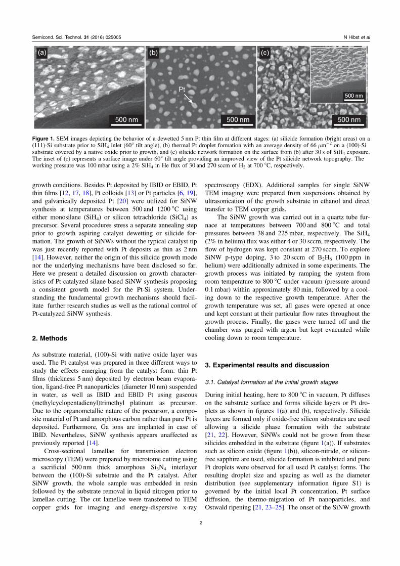
During initial heating, here to 800 °C in vacuum, Pt diffuseson the substrate surface and forms silicide layers or Pt dro-plets as shown in figures 1(a) and (b), respectively. Silicidelayers are formed only if oxide-free silicon substrates are usedallowing a silicide phase formation with the substrate[21, 22]. However, SiNWs could not be grown from thesesilicides embedded in the substrate (figure 1(a)). If substratessuch as silicon oxide (figure 1(b)), silicon-nitride, or silicon-free sapphire are used, silicide formation is inhibited and purePt droplets were observed for all used Pt catalyst forms. Theresulting droplet size and spacing as well as the diameterdistribution (see supplementary information figure S1) isgoverned by the initial local Pt concentration, Pt surfacediffusion, the thermo-migration of Pt nanoparticles, andOstwald ripening [21, 23–25]. The onset of the SiNW growth
Figure 1. SEM images depicting the behavior of a dewetted 5 nm Pt thin film at different stages: (a) silicide formation (bright areas) on a(111)-Si substrate prior to SiH4 inlet (60° tilt angle), (b) thermal Pt droplet formation with an average density of 66 μm−2 on a (100)-Sisubstrate covered by a native oxide prior to growth, and (c) silicide network formation on the surface from (b) after 30 s of SiH4 exposure.The inset of (c) represents a surface image under 60° tilt angle providing an improved view of the Pt silicide network topography. Theworking pressure was 100 mbar using a 2% SiH4 in He flux of 30 and 270 sccm of H2 at 700 °C, respectively.
2
Semicond. Sci. Technol. 31 (2016) 025005 N Hibst et al

process, initiated by the inlet of gaseous SiH4, induces the Ptdroplets toform a Pt silicide phase at temperatures between250 and 400 °C [26]. It is expectedthat first the Pt2Si phase isformed, followed by a PtSi phase as soon as all available Pt isconsumed [15, 27–29]. As some oxygen is present, which canbe commonly assumed for systems operating above ultra-highvacuum, several Pt silicide phases may coexist [27]. Never-theless, the catalyst phase is denominated as PtSi in the fol-lowing according to [12] and [15]. The Pt droplets,originating from the dewetted 5 nm Pt thin film, are sig-nificantly changed due to incipient Pt silicide formationwithin the first 30 s of the growth process (figure 1(c)).Although first nuclei of SiNWs may be assumed, the initiallyseparated Pt droplets coalesce forming a rough PtSi networkat the surface (figure 1(c) inset).
3.2. Pt-catalyzed SiNW growth modes
Distinct SiNW growth was observed after 60 s of growthyielding SiNWs with already up to 4 μm in length(figure 2(a)). However, only a few SiNWs grow in a straightmanner away from the surface and not all of them seem tohave a catalyst tip. A significant numberof SiNWs grow-laterally across the surface in an undulated manner, suggest-ing unstable growth conditions or the growth ofpolycrystalline SiNWs. Also, the shape of the Pt silicidecatalyst seems to vary (figure 2(a) inset) indicating differentcrystallographic orientations [30] between Pt silicide phaseand SiNW as observed before for Pt [12], Pd [31], and Ni [32]silicides. The predominant silicide morphology and orienta-tion is most likely affected by the initial Pt droplet formationconditions [30] such as annealing in hydrogen [12] or undervacuum. The substrate as an effective silicon source was ruledout by growth experiments without SiH4 maintaining all otherparameters. Regardless of the growth time, no SiNW growthwas observed. Moreover, in the presence of SiH4, usingsilicon-free sapphire as a substrate, SiNWs growth was
observed as equivalentto silicon-based substrates. Theimportance of Pt for the SiNW growth becomes evident iflocalized Pt spots, here deposited by EBID, are used. Here,SiNW growth occurs solely confined to formerly Pt coveredlocations as shown in figure 2(b).
After extending the growth time to 1 h, two distinct typesof single-crystalline SiNWs were observed as indicatedexemplary in figure 2(b). The first type of single-crystallineSiNWs has top diameters of 80 to 100 nm and exhibits a Ptsilicide catalyst at the tip (figure 3(a)). Due to post-growthanalysis, it still remains unclearwhether the catalyst droplet isliquid or solid during growth. According to the phase dia-gram, the lowest melting point derived from the bulk phasediagram exists for a Pt-rich eutectic phase with 23 at.% Si inPt melting at 830 °C [15]. However, this phase is not expectedto precipitate Si. To precipitate a pure Si phase, a PtSi phaseappears to be mandatory. The melting points of PtSi and itseutectic phase with Si are 1229and 979 °C, respectively [15]and will not differ significantly taking the nanoscale dimen-sion of the droplets into account [33]. Therefore, a VSS-modeappears reasonable for this type of SiNW growth at 700 °Cdenoted as VSS-SiNW in the following.
The VSS-SiNWs are tapered with a diameter decreaseover length of approximately 15 nm μm. The tapering can beprimarily linked to Si deposition by thermal SiH4 decom-position at the SiNW sidewalls. Dissolution of the catalyst inthe SiNW should be ruled out as Pt could not be detectedwithin the SiNW using TEM/EDX. However, some SiNWsexhibit an additional polycrystalline segment at their top withcrooked and tapered morphology as exemplary shown infigure 3(b). The tapering of these polycrystalline regions ismore distinct compared to the single-crystalline part due tothe incorporation of Pt into the Si. Therefore, the final tipdiameter is significantly smaller than the top diameter of thesingle-crystalline segment. The growth of these polycrystal-line regions might be triggered by the drop of both
Figure 2. (a) SEM images of SiNWs after 60 s of the growth. The inset of (a) shows the surface under 60° tilt angle. The arrows indicate theexistence of different silicide catalyst morphologies. (b) SEM image of SiNWs grown for 1 h from a single Pt dot deposited by EBID. Twosingle-crystalline types of SiNWs were observed as indicated by the arrows. The result is representative for other Pt deposition forms anddemonstrates furthermore that SiNW growth is confined to areas exhibiting Pt deposits or Pt silicides.
3
Semicond. Sci. Technol. 31 (2016) 025005 N Hibst et al

temperature and SiH4 partial pressure inside the chamber atthe end of the growth sequence. Consistent with [29] and[34], an approximately 3.5 nm thick amorphous SiO2 layer atthe catalyst surface indicates the silicide nature of the catalyst(figure 3(a), marked by an arrow).
Besides PtSi catalyzed VSS-SiNWs, a second and so farundescribed type of single-crystalline SiNWs exists. This typeexhibits larger diameters between 100 nm and 1 μm, is sig-nificantly shorter, and lacks a silicide catalyst tip. The SiNWtip is instead decorated with a blunt polycrystalline segmentof variable length from about 100 nm up to 1 μm (figure 3(c)).TEM/EDX could not detect any Pt in this kind of SiNW,neither at the tip of the nanowire nor at the interface betweenthe poly- and single-crystalline part (EDX data available insupplementary information figure S2). Similar SiNW growthcharacteristics were reported for TiSi2 islands but lackedagrowth model [35]. Although no silicide or Pt seems to bepresent in the SiNW, significant amounts of Pt silicidesremain beneath the SiNWs at the substrate surface buried by apolycrystalline Si layer or embedded in it as shown infigure 3(d). The growth of single-crystalline SiNWs from asilicon deposit in the presence of a Pt silicide phase showssimilarities with Pd [36] and Ni [32] silicide-mediated crys-tallization (SMC) utilized to transform amorphous siliconfilms into polycrystalline films. In the following, this secondtype of SiNW is therefore denoted as SMC-SiNWs to dis-tinguish them from the VSS-SiNWs, although the VSS-SiNWmode can also be explained by SMC [31].
The proposed growth model for VSS and SMC-SiNWs isbased on the assumption that the initial PtSi crystals have aspecific orientation. The growth process comprises (i) gaseousSiH4 transport and adsorption onto the catalyst or in itsvicinity, (ii) decomposition of SiH4 releasing free Si, (iii)diffusion of Si towards or across the PtSi catalyst and finally,(iv) precipitation of a SiNW. The differences in surface freeenergy between the PtSi/substrate, PtSi/amorphous-Si, andPtSi/crystalline-Si interfaces can be considered as the overalldriving forces for directed and opposing solid-state diffusionof Si and Pt [32].
In analogy to NiSi2-SMC, the lowest surface free energyis assumed to exist for the PtSi/crystalline-Si interface.Therefore, free or amorphous Si will be consumed by the PtSicatalyst, an orthorhombic crystal [37], while simultaneouslycrystalline diamond cubic Si is precipitated. Based on theavailable lattice sites, different growth velocities and direc-tions, as well as Si crystal orientations have to be assumed asobserved for the crystallization of amorphous Si films assistedby NiSi2 [32]. To nucleate a single-crystalline SiNW exhi-biting the PtSi catalyst at the tip, stable PtSi droplets mustexist on the surface, which precipitate crystalline Si towardsthe substrate while the catalyst moves continuously awayfrom the surface fed by the SiH4. Other Pt silicide crystalorientations would result in lateral silicon crystallization orgrowth of heavily kinked SiNWs (cf figure 2(a)). TerminatedVSS-SiNW growth due to unstable growth conditions ismostlikely the reason for the observed PtSi inclusions in thepolycrystalline Si overgrowth (cf figure 3(d)). The growth ofVSS-SiNW using an SMC model is supported by the needle-shaped crystal formation exhibiting a NiSi2 tip, which wasobserved for SMC of amorphous silicon films [32]. However,the growth of SMC-SiNWs having polycrystalline tips is notdescribed yet in connection with SMC to the best of ourknowledge. The formation of silicide networks during theinitial growth stages requires that Pt diffuses from the dropletsinto thermally deposited silicon on the substrate surface. Sicrystals are precipitated but the catalyst stays at the substratesurface, which could be simply due to its crystallographicorientation or inhomogeneities of the silicide network. Therole of oxygen must be further investigated in this context.Repeated precipitation of Si crystals at the silicide top surfacecan trigger needle-shaped crystals [32], forming the poly-crystalline tip of SMC-SiNWs. As described for Pd silicidecatalyzed SiNWs [31] and PtSi droplets on a silicon surface[37, 38], the silicide/silicon interface is highly dynamic andcan readily reshape to lower the surface free energy or toreach a favored silicide/silicon interface state. Once a pre-ferred orientation is precipitated, the SiNW will elongate assingle-crystal. Notably, in addition, some SMC-SiNWs
Figure 3. TEM images of the two types of single-crystalline SiNWs: (a) VSS-SiNW with a silicide catalyst at the tip, (b) VSS-SiNWexhibiting a polycrystalline, highly tapered tip extension with catalyst tip, and (c) SMC-SiNW with a blunt, polycrystalline tip without a PtSicatalyst at the tip. (d) TEM cross-section showing a PtSi layer formed between a silicon nitride substrate surface and the polycrystalline Siovergrowth (1 h growth time). The amorphous silicon nitride substrate layer was required for the TEM sample preparation. Also, a PtSiinclusion is clearly visible. (e) TEM image of an SMC-SiNW with a polycrystalline intermediate section.
4
Semicond. Sci. Technol. 31 (2016) 025005 N Hibst et al

exhibit a polycrystalline segment within the nanowire(figure 3(e)), which can be attributed to growth instabilitiescausing a temporal loss of the preferred crystal orientation. Itstill remains unclear if SMC-SiNWs are nucleated from asingle silicide crystal or if they are fed collectively from thesurrounding matrix. In order to illustrate the growth of VSS-and SMC-SiNWs as well as terminated SiNW growth, asimplified schematic is given in figure 4.
3.3. Influence of local Pt concentration, temperature, SiH4
partial pressure, and doping on the growth modes
The local Pt concentration prior to silicide formation or sili-con crystallization appears fundamental for both SMC-SiNWand VSS-SiNW growth. At higher Pt concentrations, faster
nucleation of SCM-SiNWs can be assumed and stable PtSidroplet formation should become favorable, as required forVSS-SiNW synthesis. Using IBID PtC, a distinct thicknessgradient was generated in the form of a chessboard-like pat-tern as previously reported [14]. The deposited patterns havea Pt content of about 35–45 at.% [39]. If the height increa-sedfrom about 2 to 3 nm, exclusively SMC-SiNWs withhomogeneous but short length was observed (figure 5(a)). Atincreased heights of about 4to 6 nm, a co-appearance of bothSMC- and VSS-SiNWs was observed as expected(figure 5(b)). Notably, the thickness difference of only about2 nm is affecting the length of the SiNW drastically. A furtherincreased height (gradient from 6to 13 nm) reflecting anoverall higher amount of Pt further promotes the VSS-SiNWgrowth but is still accompanied by SMC-SiNW growth asshown in figure 5(c).
Besides the Pt content, the temperature and the SiH4
partial pressure could potentially influence the effectivenessof the growth mechanisms and alter the SiH4 decomposition,the silicide phase formation, and the SiNW precipitation.Changing the growth temperature from 700to 800 °C in stepsof 20 K revealed that the overall density of SiNWs is highestaround 720 °C resulting in the longest VSS-SiNWs with anaverage length of 15 μm after 1 h (figure 6(a)). Withincreasing temperature, VSS-SiNW growth appears to becontinuously hampered so that at 780 °C almost exclusivelySMC-SiNWs are present (figure 6(b)). This indicates thatthermal SiH4 decomposition rate is another important para-meter. Therefore, at 800 °C no SiNW nucleation is observed(figure 6(c)).
Reducing the SiH4 partial pressure at 720 °C from0.14 mbar down to about 0.01 mbar by about one order ofmagnitude reduces the absolute number of SiNWs as well astheir length by about one order of magnitude (figure 6(d)). Anincrease of the SiH4 partial pressure from 1.1·10−2 mbar bya factor of two (figure 6(e)) or six (figure 6(f)) leads toincreased SiNW growth rates but hardly affectsthe ratio ofVSS- and SMC-SiNWs.
The control over both the SiNW morphology and theirelectronic properties is a prerequisite for the application ofSiNWs in electronic devices. The admixture of phosphine for
Figure 4. Schematic illustration depicting the proposed SMC-growthmechanism for VSS- and SMC-SiNWs: (a) Pt droplet formation onthe surface, (b) Pt silicide formation and thermally induced Sideposition on the substrate due to SiH4 inlet, (c) silicide dependentSi crystal precipitation leading to VSS-SiNW (left), SMC-SiNWswith a polycrystalline tip (center) and unstable SiNW growth (right),and (d) single-crystalline elongation of VSS- as well as SMC-SiNWsand termination of unstable SiNW growth in the Si overgrowth.
Figure 5. (a) to (c): SiNWs grown from a chessboard-like PtC pattern exhibiting a thickness gradient. The PtC square with the lowestthickness is at the top right and the highest at the bottom left corner ranging (a) from 2 to 3 nm, for (b) from 4 to 6 nm, and for (c) from 6to13 nm. All images are recorded under 52° tilt angle and all scale bars represent 10 μm. The average height of the PtC deposits was measuredby atomic force microscopy.
5
Semicond. Sci. Technol. 31 (2016) 025005 N Hibst et al

n-type doping of Si completely inhibited the SiNW growth.This may be related to an accumulation of phosphorus at thePtSi/Si interface [40] suppressing the nucleation of SiNWs. Asimilar effect is not reported for boron [41]. Boron-dopedSiNWsynthesis, using a silicon/boron gas phase ratio of400:3, was realized without any observable impact onto thegrowth mechanisms or the morphologies in comparison tointrinsic SiNWs. The detailed investigation of the electronictransport properties of boron-doped VSS- and SMC-SiNWswill be addressed in futurestudies.
4. Conclusion
The Pt-catalyzed growth of single-crystalline SiNWs wasinvestigated. Consistent withprevious studies, single-crys-talline SiNWs were grown exhibiting the well-known catalysttip. The growth mode for these SiNWs appears to be VSSrather than VLS. Besides the VSS-SiNWs, a so far unreportedtype of single-crystalline SiNWs was studied having a poly-crystalline tip instead of a Pt silicide. Inanalogy to thecrystallization of amorphous Si thin films by silicides such asNi2Si, a silicide-mediated crystallization growth mode, drivenby directed solid-state diffusion, was proposed also com-prising the VSS-SiNW growth. The influence of substratematerial as well as the type of the Pt catalyst depositionincluding thin films, nanoparticles, and beam-deposited Ptwas studied. Except for pure Si substrates, no significantinfluence on the overall SiNW growth characteristics wasobserved. It was demonstrated that higher local Pt con-centrations promote the nucleation of VSS-SiNWs, which
was attributed to the formation of stable PtSi droplets ratherthan silicide networks spreading across the substrate surface.The derived growth characteristics should inspire more fre-quent functional implementation of Pt-catalyzed SiNWs infuture.
Acknowledgments
We gratefullyacknowledge the Focused Ion Beam CenterUUlm, which is supported by the FEI Company (Eindhoven,Netherlands), the German Science Foundation (INST40/385-F1UG), and the Struktur- und Innovationsfonds Baden-Württemberg. In addition, we thank Eberhard Schmid fromthe Central Facility for Electron Microscopy at Ulm Uni-versity for the lamellae preparation, Dr Philipp Wagener fromthe University of Duisburg-Essen for providing the platinumnanoparticles, and Dr Sebastian Gutsch from the IMTEKFreiburg for fruitful discussion. The financial support by theGerman Federal Ministry of Education and Research (BMBF:NanoMatFutur FKZ 13N12545) is gratefully acknowledged.
References
[1] Yao J, Yan H, Das S, Klemic J F, Ellenbogen J C andLieber C M 2014 Nanowire nanocomputer as a finite-statemachine Proc. Natl. Acad. Sci. USA 111 2431
[2] Schmidt V, Riel H, Senz S, Karg S, Riess W and Gösele U2006 Realization of a silicon nanowire vertical surround-gate field-effect transistor Small 2 85
Figure 6. SiNWs grown at different temperatures, SiH4 partial pressures, and growth times. For the samples shown in (a) to (c), thetemperature was varied as indicated at a SiH4 partial pressure of 0.14 mbar and a respective diborane partial pressure of 4.70·10−4 mbar.The SiNWs shown in (d) to (f) were grown at a constant temperature of 720 °C at the indicated SiH4 partial pressure and diborane partialpressures of (d) 4.1·10−5 mbar, (e) 8.1·10−5 mbar, and (f) 2.4·10−4 mbar. The growth times are 60 min in (a) to (e) and 30 min in (f).
6
Semicond. Sci. Technol. 31 (2016) 025005 N Hibst et al

[3] Garnett E C, Brongersma M L, Cui Y and McGehee M D 2011Nanowire solar cells Annu. Rev. Mater. Res. 41 269
[4] Zhang G-J and Ning Y 2012 Silicon nanowire biosensor and itsapplications in disease diagnostics: a review Anal. Chim.Acta 749 1
[5] Shehada N, Brönstrup G, Funka K, Christiansen S, Leja M andHaick H 2015 Ultrasensitive silicon nanowire for real-worldgas sensing: noninvasive diagnosis of cancer from breathvolatolome Nano Lett. 15 1288
[6] Wagner R S and Ellis W C 1964 Study of the filamentarygrowth of silicon crystals from the vapor Appl. Phys. Lett.4 89
[7] Lensch-Falk J L, Hemesath E R, Perea D E and Lauhon L J2009 Alternative catalysts for VSS growth of silicon andgermanium nanowires J. Mater. Chem. 19 849
[8] Schmidt V, Wittemann J V, Senz S and Gösele U 2009 Siliconnanowires: a review on aspects of their growth and theirelectrical properties Adv. Mater. 21 2681
[9] Sprokel G J and Fairfield J M 1965 Diffusion of gold intosilicon crystals J. Electrochem. Soc. 112 200
[10] Wang B, Stelzner T, Dirawi R, Assad O, Shehada N,Christiansen S and Haick H 2012 Field-effect transistorsbased on silicon nanowire arrays: effect of the good and thebad silicon nanowires ACS Appl. Mater. Interfaces 4 4251
[11] Lisiak K P and Milnes A G 1975 Platinum as a lifetime controldeep impurity in silicon J. Appl. Phys. 46 5229
[12] Baron T, Gordon M, Dhalluin F and Ternon C Ferret PGentile P 2006 Si nanowire growth and characterizationusing a microelectronics-compatible catalyst: PtSi Appl.Phys. Lett. 89 233111
[13] Garnett E C, Liang W and Yang P 2007 Growth and electricalcharacteristics of platinum-nanoparticle-catalyzed siliconnanowires Adv. Mater. 19 2946
[14] Hibst N, Knittel P, Kranz C, Mizaikoff B and Strehle S 2014Beam-deposited platinum as versatile catalyst for bottom-upsilicon nanowire synthesis Appl. Phys. Lett. 105 153110
[15] Tanner L E and Okamoto H 1991 The Pt-Si (Platinum-Silicon)system J. Phase Equilib. 12 571
[16] Givargizov E I 1975 Fundamental aspects of VLS growthJ. Cryst. Growth 31 20
[17] He R and Yang P 2006 Giant piezoresistance effect in siliconnanowires Nat. Nanotechnology 1 42
[18] Jeong H, Park T E, Seong H K, Kim M, Kim U and Choi H J2009 Growth kinetics of silicon nanowires by platinumassisted vapour–liquid–solid mechanism Chem. Phys. Lett.467 331
[19] Yoo H, Lee J-I, Kim H, Lee J-P, Cho J and Park S 2011 Helicalsilicon/silicon oxide core–shell anodes grown onto thesurface of bulk silicon Nano Lett. 11 4324
[20] Cerruti M, Doerk G, Hernandez G, Carraro C andMaboudian R 2010 Galvanic deposition of Pt clusters onsilicon: effect of HF concentration and application ascatalyst for silicon nanowire growth Langmuir 26 432
[21] Yin J, Cai W, Zheng Y and Zhao L 2005 Effect of Pt filmthickness on PtSi formation and film surface morphologySurf. Coat. Tech. 198 329
[22] Wittmer M 1983 Growth kinetics of platinum silicide J. Appl.Phys. 54 5081
[23] Strobel S, Kirkendall C, Chang J-B and Berggren K K 2010Sub-10 nm structures on silicon by thermal dewetting ofplatinum Nanotechnology 21 505301
[24] Das S R, Sheergar K, Xu D-X and Naem A 1994 Thicknessdependence of the properties and thermal stability of PtSifilms Thin Solid Films 253 467
[25] Bennett P A, Chobanian J, Flege I, Sutter E and Sutter P 2007Surface thermomigration of nanoscale Pt-Si droplets onstepped Si(100) Phys. Rev. B 76 125410
[26] Takahashi Y, Ishii H and Murota J 1985 New platinum silicideformation method using reaction between platinum andsilane J. Appl. Phys. 58 3190
[27] Crider C A and Poate J M 1980 Growth rates for Pt2Si and PtSiformation under UHV and controlled impurity atmospheresAppl. Phys. Lett. 36 417
[28] Sekhar P K, Sambandam S N, Sood D K and Bhansali S 2006Selective growth of silica nanowires in silicon catalysed byPt thin film Nanotechnology 17 4606
[29] Naem A A 1988 Platinum silicide formation using rapidthermal processing J. Appl. Phys. 64 4161
[30] Yu R, Song H, Zhang X-F and Yang P 2005 Thermal wettingof platinum nanocrystals on silica surface J. Phys. Chem. B109 6940
[31] Hofmann S, Sharma R, Wirth C T, Cervantes-Sodi F, Ducati C,Kasama T, Dunin-Borkowski R E, Drucker J, Bennett P andRobertson J 2008 Ledge-flow-controlled catalyst interfacedynamics during Si nanowire growth Nat. Mater. 7 372
[32] Yoon S Y, Park S J, Kim K H and Jang J 2001 Metal-inducedcrystallization of amorphous silicon Thin Solid Films 383 34
[33] Yang W-C, Ade H and Nemanich R J 2004 Stability anddynamics of Pt-Si liquid microdroplets on Si (001) Phys.Rev. B 69 045421
[34] Kingzett T J and Ladas C A 1975 Effect of oxidizing ambientson platinum silicide formation: I. Electron microprobeanalysis J. Electrochem. Soc. 122 1729
[35] Kamins T I, Stanley Williams R, Chen Y, Chang Y-L andChang Y A 2000 Chemical vapor deposition of Si nanowiresnucleated by TiSi2 islands on Si Appl. Phys. Lett. 76 562
[36] Liau Z L, Campisano S U, Canali C, Lau S S and Mayer J W1975 Kinetics of the initial stage of Si transport through Pd-silicide for epitaxial growth J. Electrochem. Soc. 122 1696
[37] Kumpf C, Nicula R and Burkel E 1997 Growth and structure ofthin Pt2Si and PtSi layers on Si (111) and (001)characterized with in situ grazing incidence diffractionJ. Appl. Cryst. 30 1016
[38] Kawarada H, Ishida M, Nakanishi J, Ohdomari I andHoriuchi S 1986 High-resolution electron microscope studyof the PtSi-Si(111) interface Philos. Mag. A 54 729
[39] Wiedemair J, Menegazzo N, Pikarsky J, Booksh K S,Mizaikoff B and Kranz C 2010 Novel electrode materialsbased on ion beam induced deposition of platinum carboncomposites Electrochim. Acta 55 5725
[40] Kikuchi A and Sugaki S 1982 Redistribution of implantedphosphorus after platinum silicide formation and thecharacteristics of Schottky barrier diodes J. Appl. Phys. 53 3690
[41] Cohen S S, Piacente P A, Gildenblat G and Brown D M 1982Platinum silicide ohmic contacts to shallow junctions insilicon J. Appl. Phys. 53 8856
7
Semicond. Sci. Technol. 31 (2016) 025005 N Hibst et al