the mn lp filter and ge detector ..... 42 10. electron injection in a p-n junction ..... 47 ......
TRANSCRIPT

,. ~ ;,~. 4
AD-A280 687
DTIC
Thmocda&Z h0 .at @ppoved
disibti~on i's un1ialw4
94mm19375
DEPARTMENT OF THE AIR FORCE VI M NV
AIR U14VIRUSITY
AIR FORCE INSTITUTE OF TECHNOLOGY
Wright-Patterson Air Force Base, Ohio
94 624 004

AMTIDWENW944
THE EXCITATION MECHANISM OFPRASEODYMIUM-DOPED SEMICONDUCTORS
Accesion ForDISSERTATION
NTIS CRA&M
Paul L. Thee, Major, USAF UnTICr1OuAc
A r D /E I9 o 1Justificatio n~.. .. .... . ... .. ..
Distribution j
Availability Cojes
Avaii .1ddjor
Dist SXCa
Appoved for publc release; ditributin unlimitd
THlE EXCITATION M]ECHANISM OF
PRASEODYMIUM-DOPED SEMICONDUCTORS
DISSERTATION
Preeaedto tie Facuty of the Graduate School of Enginering
of the Air Force Institute of Technology
Air University
in Partial Fulfillment Of the
Requirements for the Degree of
Doctor of Philosophy
Paul L. Thee, B.S., M.S.
Major, USAF
June 1994
Approved for public release; distribution unlimited

APTr/DSAENP94O01
THE EXCrTATION MECHANISM OF
PRASEODYMIUM-DOPED SEMICONDUCTORS,
Paul L. Thee B.S., M.S.Major, USAF
Approved:
Yung Kee YeoChairman, Advisory Committee
Member, Advisory Committe
mark E. oxicy
Accepted:
Dean, Graduate School of Engieering
Blessed is the man who finds wisdom, the man who gains understanding, Wisdom issupreme; therefore get wisdom. Though it cost all you have, get understanding. Howmuch better to get wisdom than gold, to choose understanding rather than silver!
The Bible (NIV), Prov. 3:13, 4:7, 16:16
"Don't try to win the Nobel Prize, Paul. Just do some good research.. and be sure toget the Department Head on your committee."
Col. Jay Sherman, HQ AFTAC/CV, May 91
AFIT requires a great deal of sacrifice from its students, but no less from the
families and I indeed thank my wife Sonji for her sacrifices this second time through
AFIT. I am deeply grateful to Dr. Yung Kee Yeo for his tireless devotion to physics,
scientific advice and motivation. Dr. Yeo always took time to help me whether it was
a problem in my lab or advice on my career. I also greatly appreciate Dr. Robert
Hengehold for his pragmatism and encouragement over my time here at AFIT. Greg
Smith and Belinda Johnson were invaluable for without their technical assistance to
keep my laboratory running I could not have done this. The consistent encouragement
from my parents and their confidence also meant a great deal to me. Finally, I truly
thank God for the strength to endure this program.
Paul L. Thee
Dedicated to my son Brandon
Iil

page
......................................................................... i
L offig rs t o............................................ vi
List of Tab s........................................... x
US if A tre io f .......................................... xi
Absrcb..................................t..... ........ i
I. Inrdaton ............................................................. 1
Motvt on ......... v a............................... 1Probiem S tatmn a........... m......................... 3Appo c .......................................... 3Out li........................................... 4
II. Ba c k g r o ................................ n d......... 5
S1 icond1ct- Energ Bands and Impuiteu.......ti............ 5Radiative and Non-Radiative Transitions..................... 8The Crysta Field................................... 9Raue EarthEl ment ....................... .......... I11
M. Previous Woro....................................... 16
Erbxn............................................ 16P r a s e o d y m i um................................. 23
Bandgpp Engm rn g i.................................... 26
TV. EpR Im*umv p- a ml h ......a ........................ s..... 28
TiudE~aiaae Czoba lsi Gr otw th................... 29MIslrai Clumical Vapor Deposition Growth....................... 29Ion I ............................................................ 30
Ainaling........................................................ 33
V. chrcetaoTeclmiqoes ............................................. 35
iv

Sdctlve Eukation Luminmsce ...................................... 45
VI. Results and Discussion .................................. 48
Pr Liuiisca- Study of Control Sampe m ples................ 48Effect of Amnalin Conditions on Pr ILAninesene ................ 52Pr LwT esA~ Dependence on Do se...................... 57Pr Lum! ------ D epPWendece on the Host Conductivity Typ e ...... 63Pr Luinescence De p endePnceP on Host emiconducto 65Pr LuInescewe Dependence on Excitation Powew er............ 75Temperature Dependence of Pr Luaminc nce sce..............e.. 78Selective Excitation of Pr I Aminescence................................ 96Photolumninescence of Dual-doped Pr anm Er............................ 102Pbotoluminescence of Pr Codoped with Other Elements ................. 115Electroluminescence of Pr............................................. 120
VII. Conclusions and RcMme.n . ...at....ons.............................. 124
Summary ............................................................ 124Excitation Mechanism. Models ......................................... 126
R P n .................................................. 139
Appendix A: Host Information ............... ............................... 141
Appendix B: Sample Information ............................................ 142
Bibl1iography................................................................14
vita........................................................................ 156
V
Figrm Page
1. Energy Band Diagrams for an Insulator, aedonut an Metal ....... 6
2. Donor and Acceptor Energy Levels in GaAs ................................... 7
3. Host Bandgap, Trivalent Pr, and Trivalent Er Energy Levels ............... 15
4. PL Dependence of GaAs:Er on Anneal-Temperature ........................ 18
5. Energy Level Scheme of the Non-Cubic Er Complex inM BE-grown GaAs ................................................................... 20
6. Photohminesenceof GaAs:Pr .................................................... 25
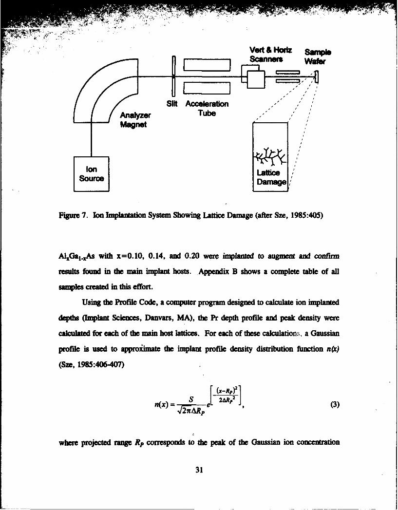
7. Ion Jmpanwt System Showing Lattice Damage ............................ 31
8. PL and SEL Experime ntA Arrangements ....................................... 37
9. Normalized System Compensation Factor for the PL Apparatus using a1000 mn LP Filter and Ge Detector .............................................. 42
10. Electron Injection in a p-n Junction ............................................... 47
11. . spectra taken at 3 K for SI-GaAs, SI-AIo.15Gao.WAs,SI-Alo.3oGa.OAs, amd SI-Alo.5Gao.oAs with Pr implanted at 390 keV witha dose of 1013/Cm2 and annealed at various temperatures................... 49
12. Photoluminescence spectra taken at 3 K for SI-GaAs implanted with Pr at390 keV with a dose of 10131cm 2 and annealed at various temperatures... 53
13. Photoluminesceme spectra taken at 3 K for SI-Alo.i0 Gao.0 5As implantedwith Pr at 390 keV with a dose of 1013/cm2 ad annealed at varioustemperatures ......................................................... 55
14. . spectra taken at 3 K for SI-GaAs implanted with Pr at390 okeV with a dose of 5 X 10¹², 1 X 10¹³, or 5 X 10¹³/cm2 an annealedat 775 OC .............................................................................. 58
vi
15. Vect. taken at 3 K for SI-Alo.la.sAs implantedwith Pr at 39 k with a dose of 5 X 10¹², 1 X 10¹³ , or 5 X 10¹³ /cm2 amda nn led at 775 °C .................................................................. 59
16. Photol• mi ý spectra taken at 3 K for SI-Alo.3OGaO.oAs implantedwith Pr at 390 keV with a dose of 5 X 10¹², 1 X 10¹³, or 5 X 10¹³/Cm 2 anda naea at 725 C .................................................................. 60
17. Photoluminescence spectra taken at 3 K for SI-Alo.5oGao.5oAs implantedwith Pr at 390 keV with a dose of 5 x 10¹², 1 x 10 13 , or 5 x I0 13/cm2 andann ale at 725 oC .................................................................. 61
18. Photokminescence spectra taken at 3 K for n-, SI-, and p-Alo.Gao.sAsimplanted with Pr at 390 keV with a dose of 5 x 10¹² and annealed at775 °C ................................................................................ 64
19. Photoluminescence spectra taken at 3 K for n-, SI-, and p-GaAs implantedwith Pr at 390 keV with a dose of I X 1013 and annealed at 775 0C ........ 66
20. Photoluminescence spectra taken at 3 K for n-, SI-, and p-Alo.5oGao. oAsimplanted with Pr at 390 keV with a dose of 5 x 10¹³ and annealed at725 oC ................................................................................ 67
21. Photoluminescence spectra taken at 3 K for SI-GaAs, SI-Alo. 5Ga.As,SI-Alo.oGao.7OAs, and SI-Ai.soGao.oAs implanted with Pr at 390 keVwith a dose of 1013/cm 2 and annealed at various temperatures .............. 69
22. Energy levels and crystal field split states of Pr3+ in AlxGaixAs compared tosemiconductor host bandgaps ...................................................... 73
23. Photoluminescence spectra taken at 3 K for SI-Alo.loGao.0 oAs andAlo.2oGao.WAs implanted with Pr at 390 keV with a dose of 1 x 10¹³/cm 2
and annealed at 750 OC ............................................................ 74
24. Behavior of the 0.779 eV peak of SI-Al0. 15Gao.5As:Pr with Ar+ laserpow er ................................................................................... 76
25. Photoluminescence spectra taken at various temperatures for SI-GaAs implantedwith Pr at 390 keV with a dose of I X 1013/cm2 and annealed at 775 C.. 84
26. Photoluninescence spectra taken at various temperatures for SI-Alo.lSGao.9Asimplanted with Pr at 390 keV with a dose of 5 x 10¹²/CM2 and annealed at775 °C ................................................................................ 86
vii
27. Photoluminescence spectra taken at various temperatures for SI-Alo.3oGao.7oAsimplanted with Pr at 390 keV with a dose of 5 x 10³/lC 2 and annealed at725 °C ................................................................................ . 88
28. The temperature behavior of the integrated luminescence intensity of peaks C,Q, and HLI in SI-Alo. 15Ga.SsAs:Pr implanted with Pr at 390 keV with a doseof 5 x 10¹²/cm2 and annealed at 775 OC ......................................... 90
29. The temperature behavior of the integrated luminescence intensity of peaks Cand Q in SI-Alo.j5Gao.8As:Pr with lines fitting to Eq (18) with E1 =9.6 meVfor peak C, and with E, = 1.4 meV and E2 =6.0 meV for peak Q .......... 91
30. The temperature behavior of the integrated luminescence intensity of peaksC and Q in SI-GaAs:Pr with lines fitting to Eq (18) with E1 = 1.2 meV andE2=22.5 meV for peak C, and E1=2.2 meV and E2 =28.9 meV forpeak Q ................................................................................ . 92
31. The temperature behavior of the integrated luminescence intensity of peak Cin SI-Alo.3oGao.7oAs:Pr with lines fitting to Eq (18) with E1 =5.6 meV... 94
32. Selective excitation luminescence intensity at 3 K for peak C in SI-Alo.5Gao.BsAs implanted with Pr at 390 keV with a dose of 5 x 10¹²/cm2
and annealed at 775 °C ............................................................. 99
33. Selective excitation luminescence intensity at 3 K for peaks C and Q in SI-GaAs-Pr implanted with Pr at 390 keV with a dose of 1 x 10¹³/cm 2 andannealed at 775 eC ...................................... 100
34. Concentration profiles of Er and Pr implanted into Alo.15Gao.95As as usedin the dual-doping study ............................................................ 104
35. PL spectra taken at 3 K from SI-GaAs implanted with Pr at 390 keV with adose of 1 X 10¹³/cm 2 , Er at 1 MeV with a dose of 5 x 10¹³/cm 2 , and both Prand Er and annealed at 750 °C .................................................... 105
36. PL spectra taken at 3 K from SI-GaAs implanted with Pr at 390 keV with adose of 1 X 10¹³/cm 2 and Er at 1 MeV with a dose of 5 x 10¹³/cm2 and annealedat various tempe t r ............................................................. 106
37. PL spectra taken at 3 K from SI-Alo.15Gao.gsAs implanted with Er at 1 MeVwith a doses of 1 X 10¹³/cm2 and 5 x 10¹³/cm 2 with amd without Pr at 390 keVwith a dose of 1 x 101 3/ctm2 and annealed at 750 °C ........................... 107
viii

•, , ,•i 2. -' -. -•
38. PL Vet takn• at 3 K from, SI-.A .•.,^ .S• imlate wit Pr at 390 keVWith a dose of 1 X l013/CM2, Er at I MeV With a dose Of 5 X l013/CM2, and bothPr and Er and annealed at 750 OC ................................................ 109
39. PL spectra. taken at 3 K from Sl-Alo.3oGao.7OAs implanted with Pr at 390 keVwith a dose of I X 10131CM2, Er at I MeV with a dose of 5 X 10131CM2, and bothPr and Er and annealed at 700 °C ................................................ 110
40. PL spectra taken at 3 K from SI-Alo.0 oGao.5oAs implanted with Pr at 390 keVwith a dose of I X 1013 /cm2, Er at I MeV with a dose of 5 x 10' 3/cm2 , and bothPr and Er and annealed at 700 OC ................................................ 109
41. PL spectra taken at 3 K from SI-AlxGal-xAs with xm 0.00, 0.15, 0.30, and 0.50implanted with Pr at 390 keV with a dose of 1 X 10/3/Cmm 2 and Er at b MeV witha dose of I X 103/CM2 and annealed at Various pr.... .................. 112
42. PL spectra taken at 3 K from SI-AlxGa1 xAs with x-=0.00, 0.15, 0.30, and 0.50implanted with Pr at 390 keV with a dose of 1 X 101 3/cm2 and Er at 1 MeV with
a dose of 5 X 101 3/Cm2 and annealed at various temperatures ................ 113
43. Concentration profiles of C and Pr implanted into Al0 .lao. 0 85As as used in thecodoping study ....................................................................... 117
44. PL spectra taken at 3 K of SI-GaAs implanted with Pr at 390 keV with a dose of1013/cm2 and codoped with B, C, N, 0, or F at energies indicated with a doseof 1014/cm2 and annealed at 800 C .............................................. 118
45. PL spectra taken at 3 K of SI-Alo. 14Ga.s6As implanted with Pr at 390 keVwith a dose of 1013/cm2 and Pr codoped with B, C, N, 0, or F at energiesindicated with a dose of 1014/cm 2 and annealed at 775 °C ................... 119
46. ManTech GaAs Solar Cell Structure used for Electroluminescence ........ 120
47. Mesa Diode Stucture for GaAs:Pr Electroluminescence Experiments .... 121
48. Electroluminescence and Photoluninescence from GaAs:Pr Cell #1 ....... 123
49. Above Bandgap Excitation Process of Pr Luminescence in AxGaxAS ... 129
50. Process Diagram for the Pr Excitation Mechanism in AlxGal.xAs .......... 130
51. Bound Exciton Recombination Energy Transfer Processes .................. 134
ix

Tabl Page
1. Ew y Level Term Splittings for Integral .................................... 10
2. The Ra•e Earth Elements ........................................................... 12
3. Praseodymium Energy Levels ..................................................... 13
4. Crystal Ionic Radii ................................................................... 14
5. Significant Papers on Erbium in Semiconductors ............................. 17
6. Significant Papers on Praseodymium in Semiconductors ..................... 24
7. Ptaseodymium Implant List ........................................................ 32
8. Praseodymium Implant Characteristics (390 keV) ............................. 33
9. PL and SEL Ex im l Apparatus List ...................................... 38
10. Absorption Coefficients for Argon Laser Light ................................ 40
11. Optimal RTA Temperatures for PL from Pr in SI-AlxGai.xAs Annealedfor 15 seconds ........................................................................ 56
12. Optimal Pr Dose for PL from Pr in SI-AlxGaj.xAs ............................ 62
13. Main pr3+ PL Emission Lines in SI-AlxGa1.xAs ............................... 71
14. Activation Energy Parameters for Pr PL in SI-AlxGa..xAs .................. 95
15. Erbium Implant Characteristics (1 MeV) ........................................ 103
16. Pr and Codope Element Implantion Characteristics in Alo.0 ^Ca0. 8 5As... 116
17. Summary of Significant Fimdings ................................................. 125
18. Pair Sums of Pr3+ Energy Levels ................................................. 136
x
LAM of------- --.
A1 1 01Ir ,As minduz Odlium Arsuaide, x-A1 mole fracton*a BDound Exchan
C Cuariumoc ~Cela" dogees
CB Condection BandCL & ýýI , ý -
DAP Donor-Accepeor Pair
EL Eeaoui~ecBPM Electron Parmmge ResonanceEr FrbiumESR Electron Spin RaosanceeV Electrolo-voltF PluormuclPB Free-to-BoondGa&s Galium Anmnide
wa Galium Pbosphidelop Indim PhophideK KelvinLIED Lii Emnittin DiodeLPE U~quld Phase EpilaxyF Macron (106 mefter)MbE Molecula Bea EtayIneV WMileectron-voltMOCVD Metaorganic Chemical Vapo DepositioN NitrogenNd Neodymiumam Nanometer (10-9 meter)0 OxygenPC Personal ComputerPL ltlmnceeP141 me, Temperatue-dependenPLE Pho. uineec Excitation (same as SEL)Pr PAsedmuRUS Rutberford Dubaucrig SpWAMSCOPYRE Rare Earth(s)SEL Selective Excitation Laminesg~moeSEW Scanning Electron, MicroscopeSi SiliconSims Secondary Ion MasspectrometryTDH Teprm qwdn ' HalliMeasurtmentTRW Transmission Electron MkcrscpeTm ThuliumVB Valence BandVPE Vapo Phase EpitaxyYb YOtriM=
xi
Abstract
Rare earth (RE) elements in semiconductors are interesting because their main
l s emissions are essentially t and host independent.
Additionally, some of these emissions occur in technologically valuable regions of the
infrared OR) spectrum, but luminescence intensities obtained from RE-doped
semiconductors have been very weak. This study on praseodymium (Pr) luminescence
in AlxGalixAs was designed to enhance the understanding of the excitation mechanism.
Pr was implanted at 390 keV with doses from 5 X 10¹² to 5 X 10¹³/cm 2 into GaAs
and AlxGalfxAs (x=0.15 to 0.50) wafers which were annealed using the rapid thermal
annealing (RTA) method. Low temperature photoluminescence (PL) was conducted
using an Ar-ion laser and Ge detector. PL emissions of Pr from all hosts include peaks
near 1.3 and 1.6 pim which are assigned to the intra-4f transitions of IG4-, 3H5 and3F3-I-3H4, respectively. For differing hosts the optimal RTA temperature varied from
725 to 775 °C and optimal ion dose varied between 1013/cm2 and 5 X 10¹³/cm 2.
The intensity of PL emissions depends strongly on the Al mole fraction. For
GaAs, the 1.3 yam emissions are strongest, whereas for all A1GaAs, the 1.6 pm
emissions are by far the strongest. Selective excitation luminescence (SEL)
experiments revealed that, in general, the Pr-related PL intensity is quenched when the
excitation laser energy is decreased below the value of the host free exciton energy.
Temperature dependent PL studies revealed activation energies of Pr-related traps.
Coimplantation of Pr with Er or lighter elements including B, C, N, 0, and F all
proved to quench the Pr luminescence.
An excitation model proposes that Pr luminescence can occur when the Pr can
successfully trap free carriers and form bound excitons. When the bound exciton
recombination energy is well-matched to the 4f energy levels either in combination or
singly with Auger process assistance, strong Pr emissions can occur.
xii
THE EXCITATION MECHANISM OFPRASEODYMIUM-DOPED SEMICONDUCTORS
I. IDIzndUin
For over a decade, researchers have pursued the goal of efficiently producing
light from semiconductors doped with rare earth (RE) elements. Motivated by the
possbility of fabricating RE-based LEDs and lasers operating at technologically
valuable wavelengths, they have explored the luminescent properties of REs and
proposed excitation models to explain the results. However, the goal of a practical RE-
based LED still eludes completion. Therefore, this research continues and expands the
understanding of RE behavior in semiconductors.
REs represent a potentially valuable technology, because their emissions are
very insensitive to the host type and temperature, and many of these emissions occur
near the important wavelengths of mininmm attenuation and dispersion in silica-based
fiber optics. Semiconductors are the choice as host material since, as injection mode
diodes, they can electrically pump RE luminescence.
Researchers have worked primarily on the REs erbium (Er), ytterbium (Yb),
and neodymium (Nd), but praseodymim (Pr) has received comparatively little
attention even though it has shown promising luminescent characteristics. This
experimental investigation is thus centered around mcreasing the undemanding of the
excitation mechanism of praseodymium in semiconductors.

A primary technological motivation for the effort proposed in this work is that
some infrared emissions from REs coincide with absorption minima for silica-based
fiber optics. In a 1979 paper, Miya and others described the transmission loss in silica-
based optical fibers (Miya et al., 1979:106). The minimum transmission loss is
attained at wavelengths near 1.55 microns while other lesser minimums occur at 1.2
and 1.3 microns. In addition, the minimum dispersion in silica-based fibers is at 1.3
microns (Pomrenke et al., 1991b:415). The interest in certain RE elements is derived
from these optical fiber characteristics. Erbium has been shown to emit at about 1.54
microns in several semiconductors (Pomrenke et al., 1989:339; Ennen et al.,
1983:943; Pomrenke et al., 1991b:415), while neodymiuml ha mission line at 1.1
microns in GaP and GaAs (Muller et al., 1986:2210). Praseodymium has 1.1, 1.3,
and 1.6 micron emission lines in GaAs and 1.3 micron lines in InP (Pomrenke et al.,
1991a:159). Thus efficient electro-optical RE-based luminescent devices operating at
these wavelengths would be ideally suited for systems using fiber optics.
The use of RE-doped semiconductors can then open up many opportunities for
new optoelectronic device applications. Light-emitting diodes (LEDs) and lasers based
on REs as the active media could be integrated directly onto electronic chips as near-
perfect optical fiber communications emitter sources. Optical fibers could then serve
as connections between these thermally robust devices. Light-emitting diodes operating
at these wavelengths have been fabricated for several semiconductor/rare earth
combinations and growth methods, however the reported efficiencies are far below that
required for device applications (Dmitriev et al., 1983:1201; Roland et al., 1988:956;
Klein et al., 1990:1299; Whitney et al., 1988a:740).
The application of this basic research is directed toward the long range
development of device technology for various optoelectronic and photonic devices in
AF avionics and other electronics. The temperature independence of RE emissions is
2
- . . - .
Ip" tuw in drvi subjc to &Wmal cycling or hier metouren r,
while the narrow linewlidt afforded by RE luminescence allows high bandwidth
modulation. These effects demonstrate the desirability of narrow RE emission lines in
AF electronics and communications.
An important task on the way to efficient RE-doped seniconductor devices is
the optimization of the luminescent efficiency. In order to optimize luminescent
efficiency in these materials, a correct understamding of the mechanisms by which the
energy is transferred from the lattice material to the rare earth impurites is needed. In
order to understand this excitation mechanism, basic research into the energy dynamics
of the rare earth luminescence in semiconductors is required. This effort consists of
basic research into the nature of the rare earth element praseodymium in
semiconductors. The ultimate goal is to understand the excitation mechanism
sufficiently well to selectively and significantly enhance the luminescent efficiency.
The main objective for this research was to expand the number of RE elements
explored in-depth. All efforts were pointed toward a better understanding of the RE
excitation mechanisms. Specifically, praseodymium was investigated in a manner
closely paralleling earlier erbium research. This parallel research allowed direct
comparison of results and excitation theories which will hopefully benefit both RE
research paths. Comparisons revealed common characteristics which may provide a
framework for further research.
In order to examine Pr, experimental data was gathered from Pr implanted into
several different types of semiconductor hosts. Much information was gleaned by
comparing and contrasting the behavior of Pr in these different host lattices.
3

Praseodymium was incorporated into 3 main host semicoductor materials including
gallium arsenide (GaAs), several variants of alumimnm gallium arsenide (AIGaAs), and
silicon (Si). The Pr luminescence haracteristics were studied based on anneal
temperature, Pr implant dose, host type, host carrier type, sample temperature, and
excitation energy. These results were analyzed, compared to previous work in REs,
and used to formulate a consistent excitation mechanism for Pr.
This dissertation is organized into several parts which sequentially present a
review of the background and previous work on rare earths and the results and
conclusions of this effort. First, the background of solid state physics related to this
work is reviewed in chapter II. Chapter M sumnmarizes the previous work done on the
rare earths Er and Pr in semiconductors. The methods for growth, preparation, and
characterization of the samples are discussed in chapters IV and V. The results of this
present effort are documented in chapter VI, while the conclusions and
recommendations are detailed in the final chapter.
4

• I IAX ItOUN
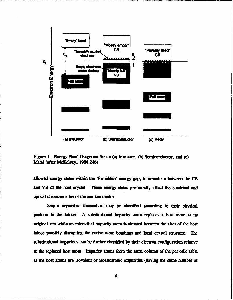
The inportman properties of sito~ht are not entirely based in their native
haateristics, but on the dramatic effects brought on by impurities in the
semicnductor lattices. It is important then to briefly outline the nature of these
impurity effects.
The electronic structure of a perfect, pure crystalline solid consists of allowed
energy bands (a group of nearly continuous energy levels) separated by forbidden
energy gaps. The distribution of electrons in these bands is described by the Fermi-
Dirac distribution and the density of allowed states function (Pankove, 1971:6-7). The
valence band (VB) and conduction band (CB) play the critical role in determining the
c of semiconductors. Separating the VB and CB from each other is the
fu mental energy gap or bandgap. In an idealized semiconductor at temperatres
very near 0 K, electrons completely fill all VB states while the CB is empty allowing
no conduction of electrons in the crystal.
In Figure 1, energy band diagrams for an insulator, a semiconductor, and a
metal are compared. In this figure, the atomic-like core bands are shown, E. is the
badigap, and sf is the Fermi Energy level. Semiconductors have a bandgap small
enough for some VB electrons to jump to the CB with reasonable thermal energy while
insulator bandgaps are so large as to pose an effective barrier between the bands. In a
metal, conducto of electrons takes place in the partially filled CB.
In a perfect semiconductor crystal, defects in the lattice or the introduction of
impurities (atoms different from the host) break the perfect lattice periodicity and
introduce localized states which decay quickly with distance outside a limited set of
neighboring lattice atoms. These localized impurity states manifest themselves as
5
-Empt bend
ef
I
(a) Inslato (b) Seffdconductor (C) metal
Figure 1. Energy Band Diagrams for an (a) Insulator, (b) Semiconductor, and (c)Metal (after McKelvey, 1984:246)
allowed energy states within the 'forbidden' energy gap, intermediate between the CB
and VB of the host crystal. These energy states profoundly affect the electrical and
optical charactetistics of the semiconductor.
Single impurities themselves may be classified according to their physical
position in the lattice. A substitutional impurity atom replaces a host atom at its
original site while an interstitial impurity atom is situated between the sites of the host
lattice possibly disrupting the native atom bondings and local crystal structure. Thetittional impurities can be further classified by their electron configuration relative
to the replaced host atom. Impurity atoms from the same column of the periodic table
as the host atoms are isovalent or isoelectronic impurities (having the same number of
6
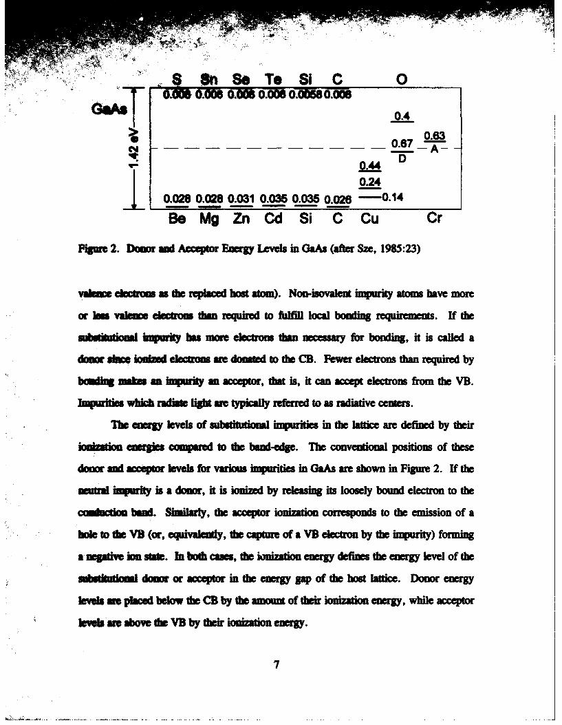
I . •n•s To Si C 00.-• t• O. 03 M o0M 0o, .o .oo6Mowe
GA 0.4 30.63-A
D
0.24
0.028 0.028 0.031 0.036 0.035 0.026 - 0.14Be Mg Zn Cd Si C Cu Cr
Figre 2. Dom ad Acceptor Energy Levels in GaAs (after Sze, 1985:23)
vaimu etroms as the replaced host atom). Non-iovalent impurity atoms have more
or less valence ekctom tdan required to f&l local boding requiremeS. if the
inaubtieml impraity has more electrom thn necessary for bonding, it is called a
donr a ion ied electrow are donated to the CB. Fewer electrons than required by
bI m lignusta impurity on acceptor, that is, it can accept eletrons from the VB.
rIdes which radiate light ae typically referred to as radiative centers.
he ewrgy levels of subItlom l impurities in the lattice are defined by their
t energie com•pmed to the band-edge. The convenional positions of these
donor anl acceptor levels for various impurities in GaAs are shown in Figure 2. If the
neutral ipw is a donor, it is ionized by releasing its loosely bound electron to the
cctlon bul Similary, the acceptor ionization corresponds to the emission of a
hol to de VB (or, equivalently, the capture of a YB electro by the impurity) forming
a negative im stme. In both caes, the ionization energy defines the energy level of the
abuhstinl donor or acceptor in the ener gap of the host lattice. Donor energy
eves awe paced below the: CB by the amoun of their ioniza•on energy, while acceptor
evels ar abov the VB by tir ionization energy.
7

it~iaiy ad Nnk.lsdibi= Trmukitim
The transitiom of electrons between allowed energy states in the lattice may be
radiative (producing a photon) or non-radiative (releasing the energy in some form
other than light). Radiative transitions can take place via a variety of paths, typically
across the energy gap or to impurity states within the energy gap. These transitions
may be CB to VB, CB to acceptor, or just about any shift of an electron between
energy levels in the lattice. Several texts extensively document the many possible
emissive transitions and the associated energies (Boer, 1990:1008-1038; Pankove,
1971:107-155).
Excitons deserve special mention because they represent a particularly important
process, especially with respect to RE luminescence. When a lattice absorbs energy
sufficient to push electrons from the VB to the CB, free CB electrons and their
associated VB holes are created. Excitons consist of an electron and a hole paired off
by coulomb itaction in which the electron and hole orbit around their center of
mass. Free excions can wander through the crystal until captured, dissociated, or
recombined. When excitons are captured by impurities (becoming bound excitons),
they can recombine to preferentially pump energy into lattice impurities. This is a
main mechanism theorized for rare earth excitation in semiconductors.
An electron can drop to an available hole state by other than radiative means.
These non-radative processes can sometimes dominate radiative processes making
them of critical interm to semiconductor luminescence studies. Major non-radiative
processes include Auger processes, transitions through localized states, and multi-
phonon processes.
In the Auger effect, the energy from the electron-hole recombination can be
absorbed by a different electron and then dissipated through phonon emission. A great
8

v-k a Aoft processes re paml, and dhe previously nmentond radiative
1w9,om may cpl to phux through a secondary electron temporarily elevated in
energ in its band (Panov, 1971:161).
Non-radiative recobination may also occur through localized defects which
produce a local contintium of states between the bands. These localized defcts may
lmlkie phsical defects in the crystal such as pores, edge boundaries, and dislocations.
When an electrw moves into this defect it looses its energy via this continuum of
States.
Traps represent another important transition effect. Traps are impurity-related
metastable states (typically non-radiative deep levels) which can capture an electron or
hole from a higher-energy state and retain it for a considerable time at the end of which
the electron or hole is released back to the higher-energy state (Pankove, 1971:370).
The electron can then make a transition to a lower-energy state via a radiative or non-
radiative process. Thus traps in semiconductors can result in delayed luminescence and
aferlow luminescence by holding potentially luminescent electrons in state for a time.
The energy transfer and excitation mechanisms of outer or valence electrons of
atoms in semiconductors are thus relatively well understood. The process which allows
energy to transfer to inner, well-shielded rare earth electron states and facilitates optical
transitions of interest in RE atoms is far from being weln understood.
The LCq a Fied
The symmetry of the location in which a RE resides in the host lattice dictates
the splitting of the energy levels and thus the number of luminescent transitions. The
energy level terms for the RE refer to the free ion energy levels. These free ion energy
levels have a 2J+1 degeneracy associated with the symmetry of isotropic 3-dimensional
space. When this free ion is placed in a host lattice, the symmetry is reduced and the
9
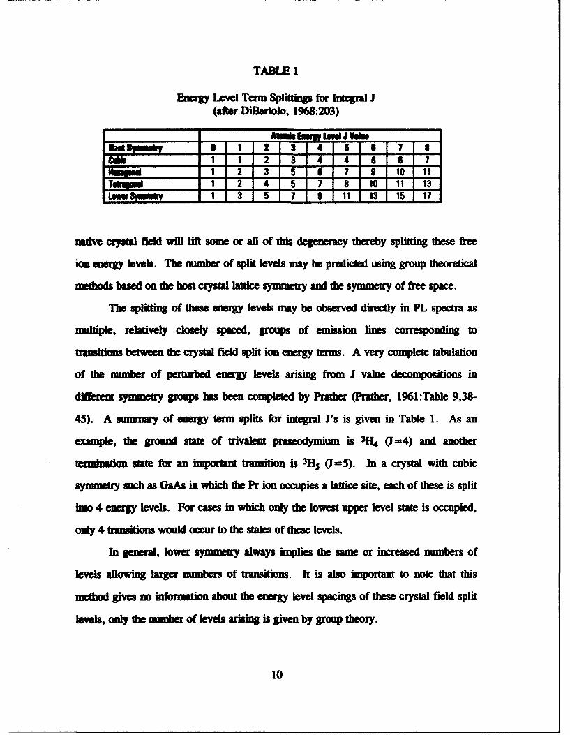
TABLE 1
Euiegy Level Term Splittings for Integral J(after DiBartolo, 1968:203)
______AM* 1"~JVdW
Id IO 1 2 3 4 5 1 7 iet1 1 2 3 4 4 6 6 7
M2 1 3 5 6 7 9 10 11TWOPW 1 2 4 5 7 8 10 11 1LoW SvWnVY 1 3 5 7 9 11 13 15 17
native crystal field will lift some or all of this degeneracy thereby splitting these free
ion energy levels. The number of split levels may be predicted using group theoretical
methods based on the host crystal lattice symmetry and the symmetry of free space.
The splitting of these energy levels may be observed directly in PL spectra as
nmltiple, relatively closely spaced, groups of emission lines corresponding to
traitions between the crystal field split ion energy terms. A very complete tabulation
of the number of perturbed energy levels arising from J value decompositions in
different symmetry groups has been completed by Prather (Prather, 1961:Table 9,38-
45). A summary of energy term splits for integral J's is given in Table 1. As an
eXample, the ground state of trivalent praseodymium is 3H4 (J=4) and another
termination state for an important transition is 3H5 (J=5). In a crystal with cubic
symmetry such as GaAs in which the Pr ion occupies a lattice site, each of these is split
into 4 energy levels. For cases in which only the lowest upper level state is occupied,
only 4 transitions would occur to the states of these levels.
In general, lower symmetry always implies the same or increased numbers of
levels allowing larger mimbers of transitions. It is also important to note that this
medthd gives no information about the energy level spacings of these crystal field split
levels, only the number of levels arising is given by group theory.
10
As previously mentioned, rare earths in semiconductors are technologically
important due to the insensitivity of 4f electron transitions to temperature and host
semicomluc'tor type. All rare earths share a closed set of inner electron shells through
4d10 (equivalent to Palladium or Pd) which do not participate in the transitions of
interest. In the neutral atomic state, rare earths have an electronic configuration of
[Pd]4fa5s25p66s2. (1)
Cerium, gadolinium, and lutetium also have a single 5d' electron in this electron
configuration. Note that the 562 and 5p6 shells are filled and are part of the xenon-like
electronic basis of REs (Table 2). Table 2 also lists the spectroscopy term symbols for
the ground state configurations in the standard form 2s+ LI in which S is the atomic
spin, L is the rotational angular momentum, and J is the total angular momentum. All
rare earths share a main valence state of 3 (the number of easily removed electrons).
These trivalent (triply ionized) RE ions have an electron configuration of
[Pd]4tfa5s 25p6 . (2)
in which the 662 shell and one 4f electron participate in the bonding. As before, the
minor exceptions are cerium, gadolinium, and lutetium with trivalent form of
4fOAs 25p6 , where the 5d1 electron is lost instead of the 4fa.
In the crystal lattice, the unfilled inner 4f electron shell of trivalent RE elements
is screened by the outer 5V2 and 5p6 shells. This screening allows only very small
lattice field-induced changes to the 4f shell energy levels. Since the 4f electron shell is
partially empty, intra-4f shell transitions to higher unoccupied 4f states may take place.
The wavelengths of interest emanate from these intra-4f shell optical transitions. The
11
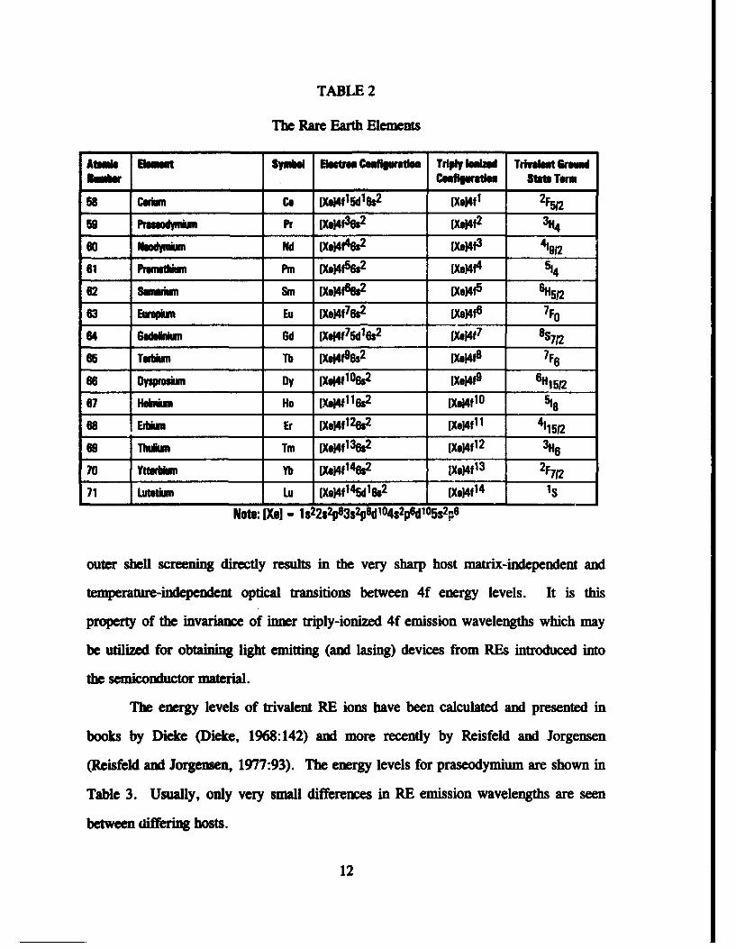
TABLE 2
The Rare Earth Elements
Atemis EleIent Sy.buI Matra Csuflguratin Triply Iouizd Tuivauot GreumiIlunr Cufguwtien State TWrO
58 Cerium Ce [Xs]4f1 5d 16 2 [XVe4f 1 2F512
59 PNUndynium Pr [XeJ4f 3 6s2 [Xo]4f 2 3 H4
60 NudynWum Nd IX.14$6s2 [XoJ4t 3 %12
61 PrOmMthuM Pm [X9]4f 5 6s2 [Xou4f4 514
62 Sniedum Sm [Xe14f 6 6s2 [XgI4f5 6H512
63 Europiun Eu [Xe]4f 7 6-2 [Xe]4f 6 7F0
64 6adduiniu Gd [XeJ4f 75d 16s2 (XSJ4f 7 8S712
65 TMhium Th [Xe]4f 96s2 [Xej4f8 7F6
66 Dysprosium Oy IXe14fl 06s2 [Xe)4f9 6H12
67 HOWm= Ho !X9]4f 1 16S2 [Xe]4f 10 518
68 ErMiun Er [Xo14f 126• [XIe4f 11 411512
69 Thulium Tm [Xe14f 1 36s2 [Xu04f 12 3 H6
70 Yterbium Yb [] 146$2 _Xe]4f13 2F71271 Lutetiun Lu [X]4f045d1682 [Xe14f 14 IS
Note: IXul - 1s22s2p63s2p6dI04s2p6dh05s2p6
outer shell screening directly results in the very sharp host matrix-independent and
te mp ture-independent optical transitions between 4f energy levels. It is this
property of the invariance of inner triply-ionized 4f emission wavelengths which may
be utilized for obtaining light emitting (and lasing) devices from REs introduced into
the semiconductor material.
The energy levels of trivalent RE ions have been calculated and presented in
books by Dieke (Dieke, 1968:142) and more recently by Reisfeld and Jorgensen
(Reisfeld and Jorgensen, 1977:93). The energy levels for praseodymium are shown in
Table 3. Usually, only very small differences in RE emission wavelengths are seen
between differing hosts.
12
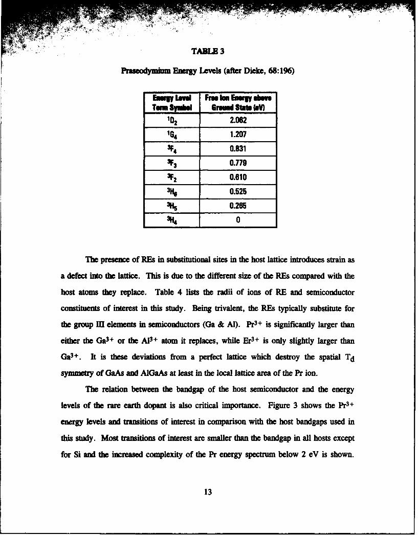
TABLE 3
Praseodymium Energy Levels (after Dicke, 68:196)
EmyW Leve Fe Is EmamvT"m Slmbe Irseud Stae 1eV)
102 2.062
164 1.207
#4 0.83133 0.779
32 0.61031te 0.5253H5 0.265
114 0
The presence of REs in substitutional sites in the host lattice introduces strain as
a defect into the lattice. This is due to the different size of the REs compared with the
host atoms they replace. Table 4 lists the radii of ions of RE and semiconductor
constituents of interest in this study. Being trivalent, the REs typically substitute for
the group M] elements in semiconductors (Ga & Al). Pr3+ is significantly larger than
either the Ga3+ or the A13+ atom it replaces, while Er3+ is only slightly larger than
Ga3+. It is these deviations from a perfect lattice which destroy the spatial Td
symmetry of GaAs and AIGaAs at least in the local lattice area of the Pr ion.
The relation between the bandgap of the host semiconductor and the energy
levels of the rare earth dopant is also critical importance. Figure 3 shows the Pr3+
energy levels and transitions of interest in comparison with the host bandgaps used in
this study. Most transitions of interest are smaller than the bandgap in all hosts except
for Si and the increased complexity of the Pr energy spectrum below 2 eV is shown.
13

TABLE 4
Cryual I•ic Radii (Weast, 14:F-l165)
A+ 0.5As3 2.22&3+ 0.81
814+.4- 0.42 2.71pr3_+ 1.013Er3 + 0.881
Erbium energy levels are also shown for comparison. This large mnuber of energy
levels has the potential for a very diverse emission spectrum limited only by transition
rules. For example, the Prs+ 3F3-+3H4 transition is spin forbidden in a free ion state,
but perbtubations intrduced by the crystal field can facilitate this transition.
14

2.5
2.0 _~wk4W
1.5 InP
411112
S~~IG4 41/
I Sllcon
103F43 4113/2
0.5 3H6
0.0_3H4 41W2 Ground0.0-pr3+ Er3 State
Host Semiconductor Trivalent Rare EarthBandgap (Low T) Energy Levels
Figure 3. Host BanIgap, Trivalent Pr, and Trivalent Er Energy Levels
15

M. pREVIOUS WORK
Much work has been done on rare earth elements in semiconductors, primarily
over the last decade. Although the vast majority of research has concentrated on Yb
and Er, limited research has also been done on Nd, Pr, and a few others. A review of
past work on the rare earths erbium and praseodymium and bandgap engineering is
presented in this chapter.
Erbium (Er) has been studied nearly as extensively as Yb. A summary of some
important papers dealing with erbium is given in Table 5. Its importance lies in the
internal transition I13/2 to 4IIs2 of Er3 + (4f01 ) producing sharp emissions near 1.54
microns. This luminescence was first reported by Ushakov et at. in 1982 for GaP:Er
and GaAs:Er (Ushakov et al., 1982:723). In both cases a weak luminescence of the Erimpurity was observed in the form of a small maximum whose profile indicated that it
probably represented an envelope of a group of closely spaced unresolved lines.
The first observation of the fine structure of sharp-line intra-4f luminescence
spectra of Er in semiconductors was reported by Ennen et al. in 1983 for Er implanted
in GaP, GaAs, InP, and Si (Ennen et al., 1983:943). Pomrenke, Ennen, and Haydl's
1986 paper showed that the PL of erbium in GaAs, InP, and GaP was critically
dependent on post-implantation annealing temperature and times (Pomrenke et al.,
1986:601). An example of their annealing study on GaAs:Er is given in Figure 4.
Their data showed that the variation in host semiconductor and treatment allowed
identification of numerous lines in all the semiconductors suggesting the existence of
several different erbium-related centers. Pomrenke, Yeo, and Hengehold later showed
that the luminescence signal was also strong from the ternary material Alo.4Ga0.6As:Er;
specifically, stronger than that from GaAs:Er (Pomrenke et al., 1991b:415).
16

TABL.E S
Sigon iePapr•s anErbs inI 1 r
UIhkhia,1082 Smeka W F L 1.541m PLEM.M 19e3 OAk, OSL . lp. UP FL Er Shmp In hwb u shummedBUI m ME EL War LED dem.trt, blw efficii Me e el Sp, 1SP kqa L 4 optkied u.odg for PL. Oi. cuten
i, !i17 elk IMP MOCOD PL Fit MOOCV PL frm ErBim, 1987 Owls LFE FLHd LFE SaAsdhr hum.... nquins .a.&v^_1 __ elk _ _ WE PL, Ed Best NMowth temparat. mi c -cetrtion,Ewa% 107 Gib W EL 1.54pm PL from neEr÷ 3 center type in
__ ta m cubic snmutry_ I= Bak inp Diffun PL First Er Offuian PL
Left' IN% __ MOCOD EL MOCVD GAtdr LED up to rom tmanR_____1 _ IO AS W EL M GWas:ErLEDat77&300Koe, 1988 8, BaAs InP,aP Verio PL I miach u*e timsfat in d hosts
NWlam., 9I=8 GaAs MOCOD PL Nrrmw, Moh ktnsity In whmn VIM - 3Sol...IM laP bo L FSIMS hIkrPL S1M studyFevur.~ IM Ga~s. Bdales BhMP. kqian FL SEM 1.54 Afl uins not unifnvdy dispersed.s T Gee MAS _ _ Er.t nicropalilesPonAlm 1M Bak he FL Free carders needed to excite Er centirsKW__IM GaAs kalntw EL Mood uGaAs:& E
Fw.cM, IWO Si bplant PL OxyW activation of Er luminescenbfi. 1991 hIP Ii EL 1.54pm EL from impact dcitatiuuift ,1991 Ml Sftd PL Effects dof cobE ts on PLWton, 1991 Si ho OLTS.. Er-ratad dfac levels in Si
k 1991 SaAs M MS Er location diplaed toward <110>KI, 1991 eaAs nqLt EPR, PL Most of Er is i Er2+ stateDenyat., 191 AM~es MBE FL Agrb LattoPooee 1092 GaA MBE TEM Abm 7 x 101 7k-3 ErAs mkrop*Md form
1992 Wks board FL Er÷ as nquiustateColon, 1992 GaAs Ilplan PLSEL Er Wnpmntation producm 2 hob traps
4 OLTS invdved in excitation of 4f hinsconsElBamuer, 1903 s fmla MSE OLTS, Er-relted hoe traps idemtifld
An inrease in the PL of Czochralski-grown Si crystals doped with erbium and
oxygen was presented in a paper by Favennec (Favennec et al., 1990:L524). They
found that oxygen implantation enhawmed the Er PL emission by an order of magnitude.
Their PL data showed that this Er luminescence was correlated with the oxygen density
in the sample suggesting the formation of Er-O radiative complexes. Coimplantation of
17

SErr m.w: IxUt
xlii
1.I6 1.57 1Jr I.1 1.54 1.S3WAVELENGTH (Ilm)
Figure 4. PL Dependence of GaAs:Er on Anneal-Tenperature (Ponrenke et a.,1986:604)
igi'rities in Er-ilnaed. Si was also studied by Michel a al. (Michel et al.,
1991:2672). This team found that implsn of erbium followed by an additional
implant yielded speceks-dependent changes in the PL intensity. The presence of light
elements such as 0, C, N, and F enhanced the Er lumincwhile heavier
elemens likMe Al, S, Ca, and P have liMe effect on the hlninescence.
18
J,
c"m"D Br-uaochad optical trans•t•mlt have also been observed for Er
lu~op~xu Inh MOCVD-grown GaAs and InP (Uwai et al., 1987:87), LPE-grown
GaAs (Bamien et at., 1987:2803), and GaAs and InP by diffusion (Zhao et al.,
1988:277). Nakagome et al. have observed a drastic change in the 1.5 micron Er-
related PL spectra for MOCVD-grown GaAs:Er when growth temperature is reduced
to 550 "C and the V/m ratio is iný d to 3 (Nakagome et at., 1988:1726). Under
these conditions, an optically efficient Er-emitting center with an extremely narrow
linewidth (less than 0.03 =m) and high peak intensity is preferentially photoexcited.
1 - has also been demonstrated from semiconductors doped
with erbium by several methods. Ennen et al. reported an MBE-grown Si:Er LED
(men et al., 1985:381). The efficiency of about 5 x 10-• was far too low for device
application. A GaAs:Er MOCVD-grown LED was demonstrated by Whitney et al. in
1988 (Whitney et at., 1988a:740), an LPE-grown version was reported by Roland et
al. in the same year (Roland et at., 1988:956), and electroluminescence at 1.54
microns was obtained from Er-implanted GaAs by Klein, Moore, and Dietrich in 1990
(Klein et al., 1990:1299). In addition, Isshiki et at. observed EL at 1.54 microns from
direct electron impact excitation of InP:Er (Isshiki et al., 1991:L225). This group
found a fairly strong EL signal at room temperature which decreased to about half theintnty obseved at 77K.
Parallel investigations concentrated on determining the exact nature of Er in
semiconductors and the energy transfer mechanism for excitation of the 4f levels. In
1987, Ennen et al. found that only one type of Er3+ center was responsible for the
1.54 micron band in MBE-grown GaAs (Ennen et al., 1987:4877). Their study
showed erbium-doped MBE-grown GaAs layers formed a number of erbium complexes
depending on the growth temperature. For the previously reported optimum substrate
grow temperature of 580 °C (Smith et al., 1987:49), only one type of luminescent
19

NHE GaAs: Er
331.7
21?.3
------- -- 0+1500.?
PLE PL
Rl.'
2•0. 1'11gb -21?. 3
- 112.3L&t
L 0
Figure. 5. E a Level ScWem of fth NOB-Cubic Er Complex in MBE-grown GaAs(Erm e al, 1987:4879)
bium caer M observed with 8 emission lines recorded from 6 K PL. The
nmltpcity Of e-- llins Wi atd that this Er3+ center occupies a position of
lower than cubic aynmmty. From then data, the researchers constructed an emurg
level WcIin for the iWnabic Er3+ complex in MBE-gown GaAs (Figure 5).
Koaneeki e a1. fwEr refined this by reportig that erbimn-irpn GaAs was
dibpbce from the sbstituioml position to the <10> chamnnel (Kozaneck et al.,
1991:763). In agrement with Pomrenke et al. (omý a, al., 1986:601), they also
found that te e cal avity of erbum disappeared as higher anealite mpe ature
movedftheerbium tward a substituional location.
Klei am! Pomareake reported on the lifetime of the Er3 + excited state in a
variety of materials in a 1968 article (Klein et al., 1988:1503). Their study showed the
20
HWbs of dW 1 ,34 excised Sat of Er3+ is about 1 millisecond for all the hosts
IhCME-grown and implanled Si:Er, MBE-gown and implanted GaAs:Er,
MOCVD-grown and implaned InP:Er, and implanted GaP:Er. This constancy of the
IIId" acroes several hosts strongly suggests that Er decay is largely radiative, that is,
there appear to be no strongly competing non-radiative decay mechanisms to reduce
this lifetime. They also repor that these PL decay times are about 100 times longer
than those from comparable InP:Yb samples. Thus Er-doped materials appear to offer
mMer potential in device applications than their Yb counterparts. Benyatoui et al.
reprted nearly the same lifetime of 1.2 milliseconds for Er in Go.%Aio.45As
(Benyattou eral., 1991:2132).
Similar to observations in InP:Yb (Korber and Hangleiter, 1988:114),
Pomrenk, Hengehold, and Yeo established that free carriers are required to excite the
rare earth centers for GaAs:Er and InP:Er along with InP:Yb, GaAs:Yb, GaAs:Tm,
and GaAs:Pr (Pomrenke ef al., 1989:339). These free carriers may be manifest in
excitation via direct capture of excitons or hot carrier impact excitation. In conclusion,
these workers propose GaAs:Er as the best candidate for devices.
With Er centers in GaAs being excited over the widest range of states,combined with the observed room temperature luminescence, longlifetimes, and the technological importance of the 1.54 micronswavelength, allows one to conclude that the GaAs:Er system shows thegreatest promise for electro-optic applications. (Pomrenke et al.,1989:344)
Favennec et al. reported in 1989 that the 1.54 micron Er-related emissions are
not uniformly spaced over the surface of a sample (Favennec et al., 1989:333). These
results were obtained from CL-SEM experiments in Er-implanted GaAs, GaInAs,
GalnAsP, and GaAIAs and imply that optically active erbium atoms could be clustered
21

in the imphited layer u -onc-particles of Er-rich compounds. Poole, Singer, and
Pader comfiniud this in MBE-grown GaAs:Er in which Er concentratiom greater than
7 x 10171= 3 ftrm ErAs m-crOcl-al (Poole et al., 1992:121).
A significant paper by Klein, Moore,. and Dietrich in 1991 reported that Er2+
was a jor player i erbium ni (Klein et a., 1991:502). They measured
the depeadese upon annmal temperature of the band-edge and Er3 + PL and EPR in Er-
inplazd GaAs and concuded that:
(1) The Er3+ PL spectrumn consists of a superposition of spectrafrno several distinct erbium sites,
(2) almost all the erbium in the sample was in the Er2+ state, and(3) the important Er3+ PL is excited from Er2+ occupied centers.
They also proposed that these Er2+ sites involve complexes of interstitial Er with
defects or impurities and the small number of Er3+ centers (<0.1% of erbium in the
.sample) occupy tetrahedral interstitial sites. In a 1992 paper, these researchers
proposed that Er3+ might, in fact, be a non-equilibrium state for above gap excitation
(Klein et a., 1992:665).
Benyattou and worbes in France suggested a model for the erbium PL
excitation preess in MBE-grown AIGaAs:Er (Benyattou et al., 1991:2132). Two
beam time-resolved PL measurements showed that there are significant losses related to
free carriers occurring in the PL excitation process. Their model proposed that bound
excitom recomine and transfer energy to the Er via an Auger recombination process
or direct energy transfer to the erbium ion.
Colon et a. proposed the first excitation mechanism for GaAs:Er in 1992
(Colon et al., 1992:671). Using DLTS measurements, this group found that erbium
implantation introduces hole traps at 35 meV and 360 meV above the valence band,
while selective excitation showed that the 4f emissions can be strongly excited with
22
h eaton en y:
1. EWcttOMM enerV greater than bandgap creates electron-hole pairs with freebola- tiffpd in the Er-related hole traps.senscaptuhns a free electronforming a bound exciton. Subsequent recombination of this pair transfers t to the4f shell via an Auger process.
2. Exkcta enerV less than bandgqp provides sufficient energy to exciteelectrons at the traps into the CB leaving a hole behind. An electron recombines withthis bound hole contributing the recombination energy to the 4f shell.
Summarizing erbium's potential importance, Taniguchi's statement in a 1991
paper is telling.
The'characteristic sharp-line 4f lumiescence has been observed fromvarious RE and M-V compounds. However, it was found that the RE-related hluinescence intensity drops drastically as the sample
mure i s, and that only GaAs:Er and InP:Er can still emitlup to room tmpear. (Taniguchi et a., 1991:2930)
(Note: Some MOCVD-grown GaP:Nd samples exhibited room temperature
luminescence as reported by Takahei and Nakagome in 1989) (Takahei and Nakagome,
1989:913). Pomrenke also echoes the importance of Er in a paper on Er, Tm, and Pr
in GaAs and AlGaAs where only Er showed emissions at room temperature (Pomrenke
et a., 1991b:415).
Praseodymium (Pr) papers are listed in Table 6. LAuminescence was first
reported in 1981 by Kasatkin et al. who reported four groups of closely spaced Pr-
23

TABLE 6
Siqnifixa Papers on Praseodymium in Semiconductors
Kdkau.1S IM P W__ PL RdstMpenduPLKnsft~i M u W__ FL PLdMcyMuhuar
kIM m iP. ZMs pImht PtCL PI ad PriJ PL rpmdhmi..W low 08".u kno FL PrNdYb soch fum Mfawui cmoym
SuhWM. im hop k* KLAM he*Pr L & noSMSsU*Pu Iwok.i Ga"S bow PtL SE Free caniws ai minw statidon muhmismPOMvuXIsola lopBGas browm PL Pr PL ~inp &so" qINPWWPm.umk% 1001b GaAs hupWn PUT) DiffuWn wisim bwe tuquratw qusdikgKathauas, 1901 uSIMs LPE Hi Trmpor pr@umds & noatuni macudnu sudyLaL 19S2 huwu LPE Hot PL Prpaying bLPE kWuErikson 1903 Bobs k* PLM -Wid FL spuctrs, fft to Dg cryut modd
based emissions from GaP near 1.3, 1.7, 2.0 and 2.3 eV (Kasatkcin et al., 1981:353).
In a unique follow-up paper 4 years later, Kasatkin reported that the Pr intracenter
luItescence had disappeared after prolonged storage (Kasatkin, 1985:1174).
Gippius et al. found that companato of lithium in Pr-doped GaP changed the
spectrum by shifting emissions to near 1.1 microns and introducing lines near 0.9
microns (Gippius et al., 1986:1196). They attributed this effect to the formation of Pr-
Li complexes, and proposed that Li plays a certain role in the energy transfer from
electron-hole pair recombination to the Pr-related centers.
Plomrenke, Hengehold, and Yeo also reported complex behavior of GaAs:Pr
with emission lines near 1.1, 1.3 and 1.6 microns (Pomrenke et al., 1989:343). By
investigating the selective excitation spectra for the strongest lInes, they found no
signfitiai excitation of the three Pr3+ emissions by DAP or lower lying states. Their
study showed that the main excitation mechanism for PO + is also through free carriers,
but states at or below the donor-acceptor states are not excluded from the excitation
24

180 IM0
V . . .. - -.. . I . . . . . I --- - -- -I . . I , .I . ., . , I . . .
0.76 0.2 0.88 0.94ENERGY (*V|
Figure 6. Photoluminescence of GaAs:Pr (Pomrenke et al., 1991a:162)
In a latter paper, Pomrenke, Hengehold, and Yeo observed characteristic 4f
emissions of Pr3+ (4f2) from GaAs (Figure 6) and InP. The 3 sets of sharp GaAs:Pr
emissions reported at 1.05, 1.35, and 1.6 microns were due to transitions between the
crystal-field-split spin-orbit levels IG4-+3H4, IG4-+ 3H5 , and 3F3-+3H4 , respectively
(Porenke et al., 1991a:161). At optimum anneal temperatures, they found no
evidence of near-band-edge emissions (DA transitions). The existence of these would
imply the presence of competing processes which favor Pr excitation over FB or DAP
recombinations. They also reported different temperature quenching behavior of these
lines. The 1.35 micron emissions disappeared around 107 K, but the 1.6 micron lines
contmiei until 174 K. The low intensity of the 1.05 micron line precluded
tm rte dependent studies. They concluded that Pr may occupy substitutional
and/or interstitial sites.
Photoluminescence studies of Pr have also been reported for InP am! IndaP. In
the only other ternary host tested for Pr PL, Lai and Chang observed no InGaP:Pr
25
iWtra-4f transitions in the 600-800 nm range (2.07-1.55 eV) (Lai and Chang,
1992:1314). It has also been found that Pr-implanted InP emissions differ from that of
GaAs:Pr. Reported emissions from InP:Pr were between 1.34 and 1.44 microns and
lacked the 1.1 and 1.6 micron signals found previously in GaAs:Pr (Solomon et a.,
1989:574).
In a most recent paper, Erickson et al. have collected a very wide spectra of Pr
in GaAs (0.49-1.49 eV). The main thrust of the paper is the theoretical calculation of
the predicted emissions using a D 4 symmetry model which has less intrinsic symmetry
than Td.
Praseodymium has been studied mainly in GaAs, GaP, and InP. Luminescence
has never been studied in silicon or ternary compounds while only PL demonstrations
have been reported from GaAs:Pr, InP:Pr and, GaP:Pr. Thus praseodymium requires
much more research.
Bandgan Engineering
An alternate method of producing luminescence from semiconductors at desired
wavelengths is bandgap engineering. In this method, compounds are fabricated to
obtain specific bandgaps which then allow strong luminescence at this bandgap energy
via electrical excitation. This is accomplished by using ternary and quaternary
compounds. Ternary Ir-V solids have 2 different group III atoms at group II sites or
2 different group V atoms at group V sites. The notation used for this is AxBI-xC or
ACyD1.y where A and B represent group HI elements while C and D are group V
elements and x and y are the mole fractions. Quaternary compounds involve 4
different elements, typically a pair of group MI's and a pair of group V's with notation
AxBI-xCy•D.y. The property of primary interest in these compounds is the variation of
the energy gap with the mixture ratio. That is, the energy gap of the alloy will assume
26
a value inumdate between the gaps of the two 'pure' semiconductors of which it is
This bandgap engineering has been studied most intensively in AlxGa.-xAs
because of its close lattice match to GaAs. This greatly facilitates the fabrication of
heterojunctions (junctions between two dissimilar semiconductors). Heterojunctions
are important because the difference in energy gaps allow high injection efficiency of
minority carriers into the lower-gap semiconductor (Pankove, 1971:197).
Semiconductor lasers based on heterostructure designs can operate on much less current
than similar homojunction lasers (Sze, 1985:268).
Rare-earth luminescence from ternary compounds have also been studied
(Pomrenke et al., 1991a:415; Favennec et al., 1989:330) and continue to be of interest
because of the aavantageous laser effects, For example Benyattou et al. found Er-
related emissions from Gao. 55Ai0 .45As at 0.98, 1.54, and 1.57 microns (Benyattou et
al, 1992:350). They conjectured that the 1.57 micron emissions emanate from Er-Al
complexes since they did not occur in GaAs. Interestingly, Tsang and Logan achieved
semiconductor lasing at 1.5 microns using GaInAsP (Tsang and Logan, 1984:1025) and
at 1.55 microns with erbium-doped GaInAsP (Tsang and Logan, 1986:1686).
However, doubts have surfaced as to whether the 1.55 micron emissions were actually
erbium-based transitions (van der Ziel etal., 1987:1313; Wu etal., 1992:456).
Bandgap engineering techniques are attractive in their versatility, however this
method will be afflicted by both temperature dependent bandgaps and relatively wide
emission linewidths due to processes contributing to band-tailing. Thus work on RE
emissions from semiconductors is still important because of their temperature
independence and narrow linewidths.
27
IV. EPFRIM NTAL SAMPI.Y.
One of the major issues to be dealt with when attempting semiconductor
research is procuring, fabricating, or growing the samples. Since the sample growth
technique and post-growth processing conditions directly affect the electrical and
optical properties of the sample, these are important issues. In this chapter, the
samples used in this research are detailed and the semiconductor host growth and rare
earth implant methods are explained.
Host Semiconductors
Praseodymium was incorporated into 3 main host semiconductor materials
including gallium arsenide (GaAs), several variants of aluminum gallium arsenide
(AlGaAs), and silicon (Si). These materials were chosen based on their important
technological applications. Bulk silicon forms a diamond crystal structure with
covalent bonding while both GaAs and AIGaAs have mixed atomic bonding, being
partially ionic and partially covalent, in a zincblende crystal structure.
GaAs is the main compound semiconductor serving as the basis of many
microwave and photonic devices. It has been heavily studied especially as the most
widely used IH-V compound in lasers and LEDs. AIGaAs is also a major compound
used in photonic devices due to its extremely close lattice match to GaAs. This allows
growth of simple heterostructure or layered devices with minimum interface defects.
AIGaAs is also used for its "adjustable" bandgap which may be varied from 1.42 to
2.17 eV (300 K) by changing the Al/Ga ratio. This allows creation of material with a
bandgap tailored to suit the electronic device. The bandgap may be fabricated to aid or
control the current injection across the junction of a semiconductor laser and, indeed,
AIGaAs has found wide applications in heterostructure lasers, LEDs, photodetectors
and solar cells (Sze, 1985:265-269; Casey and Panish, 1978:27-28). Finally, silicon is
28
cmuiy th priWM maer for semiconductor device fabrication. These thm
mateIas represent t•nolopcally the most important semiconductors in use today and
will serve as the hosts for praseodymium research conducted in this study.
l .mni l~n~~msted rzowhraldd~ Growth
Them are many so-called classical methods of crystal growth which depend on a
natural mechanism such as growth from molten solution. These methods are
extensively reviewed elsewhere (Boer, 1992; Sze, 1985). In the liquid encapsulated
Czochralski method (LEC), an apparatus called a puller which consists of a furnace
containing a crucible with a molten solution of the compound to be grown. A seed of
the compound is dipped into the solution and slowly withdrawn while rotating to create
the crystal. An inert gas is flowed over the melt and the system is typically controlled
to optimize temperature, rotation rate, gas flow, and pull speed. Progressive freezing
at the liquid-solid interface results in a single, large crystal (Sze, 1985; 304-306). For
LEC-growth of GaAs, an inert cap of liquid encapsulant of molten boron trioxide is
floated on top of the molten GaAs in order to prevent decomposition of the GaAs.
The LEC-grown GaAs wafers in this study were purchased from Epitronics
Corporation as grown by Hitachi. As reported by the vendor, the wafer thickness
varies between 627 and 636 microns, the mobility is from 7100-6800 cm 2V-'sec-, and
the resistivity is 2.3-4.5 X 10⁷ ohm/cm. Appendix A gives specific characteristics of all
wafers used in this study.
Metalorganic Chemical Yamo Detxsition Growth
Metalorganic chemical vapor deposition (MOCVD) crystal growth is achieved
via high tempeure chemical reactions of a vapor of desired compounds onto a
substrate surface. The reactions are carried out thermally with the gases flowing over a
reactor cell containing the substrate. The rate of growth is determined by
29
decomposition of the feedstock gas at or near the surface (feedstock depletion is due to
substrate surface adhesion) and the necessity of removing the reaction by-products
(Boer, 1992:185). MOCVD tends to produce excellent crystals because it operates
close to thermodynamic equilibrium. Control of layer thickness is not as precise as
other epitaxial methods such as molecular beam epitaxy. MOCVD layer thickness is
controlled simply by calibration and timing of the supply of feedstock gases.
The MOCVD-grown GaAs and AIGaAs wafers used in this study were grown
by Epitronics Corporation on LEC-grown GaAs substrates with the same
characteristics as reported above. The AIGaAs layers were generally 5000 A thick,
with doped carrier conentrations of 1 1017/cc and undoped concentrations of
<5.0X10 16/cc as reported by the vendor. Thin GaAs cap layers (50-200 A) were
grown over all AIGaAs wafers to prevent surface oxidation. Appendix A gives specific
characteristics of all wafers used in this study.
ionInlato
Ion implantation has become a mainstay method of introducing impurities into
semiconductors since the 1970s and consists of shooting energetic, charged dopant
particles into a substrate via a controlled ion beam (Figure 7). The advantages of ion
implantation are precise control over the amount of doping, better impurity profile
reproducibility, and lower temperature processing requirements compared to diffusion
techniques (Sze, 1985:382). Another pragmatic advantage is that several different
substrates of entirely different host semiconductors can be implanted simultaneously.
The praseodymium and other species used in this study were implanted by
Universal Energy Systems (UES), Dayton, Ohio under contract with ART. All
praseodymium was implanted at 390 keV. A wide variety of host lattice types were
implanted at 3 different doses as shown in Table 7. In addition, small amounts of
30
. . .. ..
•o •Vor&Hr - -Pt -'
Vert & Har sampl
=cnes wafe
Slit Acceleration ." ',
Analyzer Tube - '
Ion Lattce "Source Damage,
Figure 7. Ion Implat] o System Showing Lattice Damage (after Sze, 1985:405)
AlPa11As with x=0.10, 0.14, and 0.20 were implanted to augment and confirm
results found in the main implant hosts. Appendix B shows a complete table of all
samples created in this effort.
Using the Profile Code, a computer program designed to calculate ion implanted
depths (Implant Sciences, Danvars, MA), the Pr depth profile and peak density were
calculated for each of the main host lattices. For each of these calculations, a Gaussian
profile is used to appximate the implant profile density distribution function n(x)
(Sze, 1985:406-407)
(x-Rp?
n(x) s 2ARp2 (3)27tARp
where projected range Rp corresponds to the peak of the Gaussian ion concentration
31
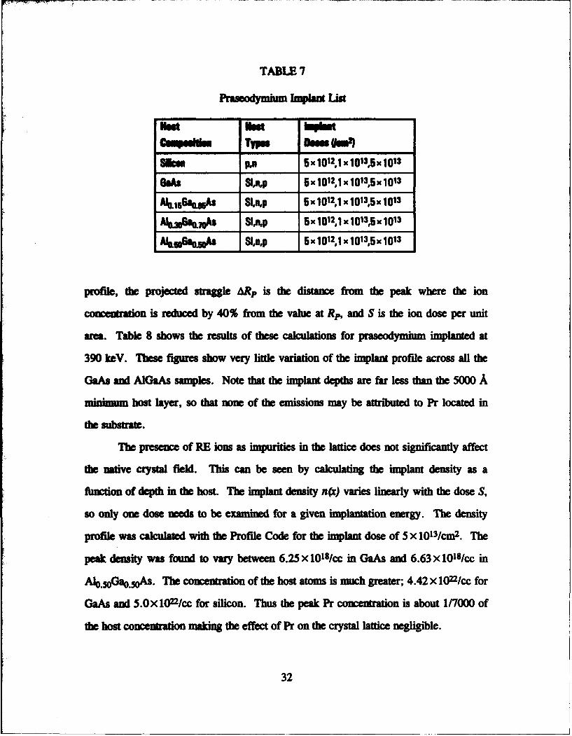
TABLE 7
Prmaodymim ImpWant Ust
bOuueduu TOWe bus US. 1)
Saim pA 5x 1012,1 x 1013,5 x 1013
GaAs SIa,p 5x 1012,1 x 103,5 x 1013
AilgG% 5As SlAP 5x1012,1x1013,5xjO11
A0.2 O6G1l 7 As SIfnp 5 x 1012.1 x 1013,5 x 1013
AI&WG@&WA I Sln,p 5x1012,1 x 1013,5 x 1013
profile, the projected straggle ARp is the distance from the peak where the ion
c r is reduced by 40% from the value at Rp, and S is the ion dose per unit
area. Table 8 shows the results of these calculations for praseodymium implanted at
390 keV. These figures show very little variation of the implant profile across all the
GaAs and AIGaAs samples. Note that the implant depths are far less than the 5000 A
minimum host layer, so that none of the emissions may be attributed to Pr located in
the substrate.
The presence of RE ions as impurities in the lattice does not significantly affect
the native crystal field. This can be seen by calculating the implant density as a
fiuction of depth in the host. The implant density n(x) varies linearly with the dose S,
so only one dose needs to be examined for a given implantation energy. The density
profile was calculated with the Profile Code for the implant dose of 5 X l013/cm2 . The
peak density was found to vary between 6.25 x 101s/cc in GaAs and 6.63 x 10¹⁸/cc in
AI.S.OGa 5 As. The concentration of the host atoms is much greater; 4.42 x 10²²/cc for
GaAs and 5.0X 10²/cc for silicon. Thus the peak Pr concentration is about 1/7000 of
the host concentration making the effect of Pr on the crystal lattice negligible.
32
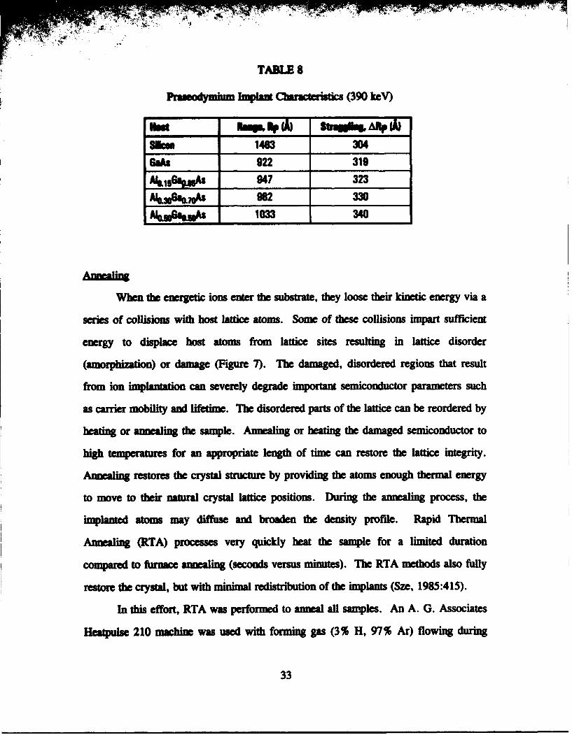
TABLE 8
ramodymium bipant Caracteristics (390 keV)
SUNl. 1463 3M4Bobs 922 319ALt 947 323
A0GknAs 982 330A ummS133 340
When the energetic ions enter the substrate, they loose their kinetic energy via a
series of collisions with host lattice atoms. Some of these collisions impart sufficient
energy to displace host atoms from lattice sites resulting in lattice disorder
(amorphization) or damage (Figure 7). The damaged, disordered regions that result
from ion implantation can severely degrade important semiconductor parameters such
as carrer mobility and lifetime. The disordered parts of the lattice can be reordered by
heating or annealing the sample. Annealing or heating the damaged semiconductor to
high temperatures for an appropriate length of time can restore the lattice integrity.
Annealing restores the crystal structure by providing the atoms enough thermal energy
to move to their natural crystal lattice positions. During the annealing process, the
implanted atoms may diffuse and broaden the density profile. Rapid Thermal
Annealing (RTA) processes very quickly heat the sample for a limited duration
compared to furnace annealing (seconds versus minutes). The RTA methods also fully
restore the crystal, but with minimal redistnrbution of the implants (Sze, 1985:415).
In this effort, RTA was performed to anneal all samples. An A. G. Associates
Heatpulse 210 machine was used with forming gas (3% H, 97% Ar) flowing during
33
a sl. owin noge gas was used for pe- and post-anneal purging. Samples
wwe amiMd face up and covered with a capping wafer of GaAs to minimize As boil
off sad pI tial chemical cIuta mlnafio. The ramp up of the sample temperature from
ambient to desired annealing point ranged from 30 to 38 seconds, while cool down to
300 oC generally took about 4 minutes. The variance of the annealing temperature as
reported by the RTA system was always between -5 to +7 °C of the target
34

V. -r • •x MS
severa eWpen al techniques hve bee developed to analyze the
laacterlaic of 1mio1uctos. Each has particular strengths and applications, and
gives R information. It is adv to employ more than one technique on a
given problem sinee, usually, no single method will yield all the vital evidence. The
teciniques used in this research are described in this chapter.
Photoluminescence spectroscopy is the most common technique for investigating
the electronic transitions in semiconductors. In this method, electrons are excited from
their gpound state to higher energy (non-equilibrium) states by photon absorption. The
radiated light spectrum resulting from recombination of these excited electrons with
holes can reveal much information about the electronic processes occurring in the
semiconductor.
PL measurenuns are practiced at low sample temperatures for two principal
reasons. The first strong advantage of low temperature measurements is to inimi
broadening of otherwise sharp spectral features by lattice vibrations (phonon
absorption). The vibration of neighboring ions creates a changing crystal field at the
place of rare earth ions which is not the same for all ions. This broadens the resulting
spectral lines (Dieke, 1968:32). Liquid helium cooling of the sample to 4 K is
effective for minimizing this line broadening. Low temperture are also desirable
because mat substances have a fairly closely spaced group of levels from which
absot can take place. The occupation of levels greatly decreases with increasing
energy according to Boltzmann's exponential law. By keeping electrons mainly in the
ground state via very low temperatures, the spectral analysis is simplified by
35

e~~lmthe M n cq licatlon of overlapping lines from nuiltipl thermally populated
lowr Irick (Dish, 1968:32).
.A~i, L.. In PL, excitation with photom of energy greater than the
baufltip produces a mm-equifim concentratiom of electrons and holes. At low
t, these mady form excions which can decay directly or after capture by
impurities or deftm (Lightowlers, 1990:1161). The fate of the electron-hole pairs
created by the laser photons depends on the nature of the semiconductor. In a high
purity material (relatively small impurity concentrations), these electrons and holes pair
up to form free excitons which subsequently decay producing free exciton
lm 4. Materials containing significant donor or acceptor impurity
oeations (>1015 cm-3) have virtually all of these free excitons captured by
impurities giving rise to impurity-specific bound exciton luminescence (Stradling and
Klipstein, 1990:143). Because of the competition between these various capture
mechanisms and both radiative and non-radiative decay mechanisms, PL is not
generally a quantitative technique in that absolute line intensity is rarely used. The
strength of PL is in unambiguous identification of transition energies and the
consequent determination of relative energy levels.
The sample temperatre and excitation energy and power may also be varied in
PL experiments in order to obtain more information about the energy levels in
luminescent centers.
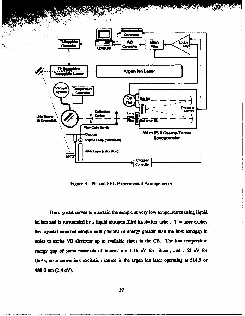
PL E!••1 _ wsApm_ . Figure 8 shows the experiet arrangement
used for PL spectroscopy in this effort (the tunable Ti:Sapphire laser pumped by the
argon laser is required for SEL). The specific apparatus is listed in Table 9.
36
f 7f
MM Argon Ion Law
vauu Toniper"x
Go EAsw
DLe Focumi
Ll DM~Ws Ca4s0iOM O M
a IWSt , Fiair~aoS
ChopW314 mn M6. Czerny-Tumer
Figure 8. PL and SEL Experimental Arrangements
The cryosta serves to maintain the sample at very low temperatures using liquid
helium and is surrounded by a liquid nitrogen filled insulation jacket. The laser excites
the cryostat-mounted sample with photons of energy greater than the host bandgap in
order to excite VB electrons up to available states in the CB. The low temperature
energy gap of some materials of interest are 1. 16 eV for silicon, and 1.52 eV for
GaAs, so a convenient excitation source is the argon ion laser operating at 514.5 or
488.0 mn (2.4 eV).
37
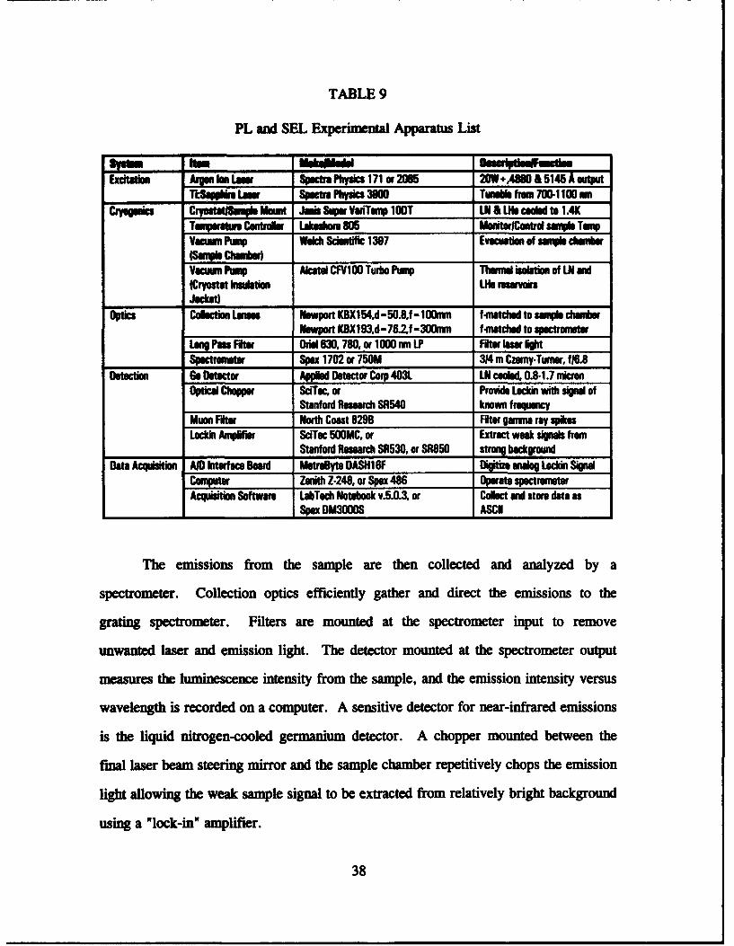
TABLE 9
PL and SEL Eprmntal Apparatus List
Excittio Ag nU Spectr Physic 171 or 2065 20W_,480___545 ___
___________ w Spectr Physic 3900 Tumalk from. 700-1 100 onCryogoies Cyb uhMntJmnsSipr Var~n~wnlOT LN & LII. cooled to 1UK
Tumgmratu Central., Lakuseora 805 MonitoriControl sanqiae TuqVacuum Purnq Welch Sciont-ifc 1397 Evacuation of sampl Ah~
Vacuu Pump Alcatu CF V100 Turbo Pump Thorul isoation of Ltd and(Cryostat Iunsoation V Usevor
optics Clelction Lam..t Nawtport KBXI 54Ad- 50.8,f - IO~kaun fUmaotchod to suMb rla chume_____________Nawport KBX193,d-75.2.f-Mmau fimatchsd to spectrornsturLogPnFtr Oriu 830, 780, of 1000 ran LP Fdtor lase W~,
_____SpectronuItar Spas 1702 or 750M 314 mn Czerny-Tuurner f16.8Detect..n so Detectr Appled Detecor Corp 403L Ltd cooled 0.8-1.7 micon-
OptcalChopper SciToc, or Provids Lockin with signa of_________Stanford Research $8540 known frequency
Muon Fit.r North Coast 829B Fitar ganmna ray spkusLocki. Ampila SciTec 500MC, or Extract weak signals from
______ ________Stanford Resarch 58530, or 8R850 strong backgroundData Acquisition AID hItadace Board MetraByte BASHI OF D~ igitiealo Lock.n Signa
Conqatr Zenith Z-248, or Spas 486 Operate specromeoterAcquisition Software LabTech Notebook v.5.0.3, or Clc n tr aaa
________ __________Spas DM3000S ASCII
The emissions from the sample are then collected and analyzed by a
spectrometer. Collection optics efficiently gather and direct the emissions to the
grating spectrometer. Filters are mounted at the spectrometer input to remove
unwanted laser and emission light. The detector mounted at the spectrometer output
measures the luminescence intensity from the sample, and the emission intensity versus
wavelength is recorded on a computer. A sensitive detector for near-infrared emissions
is the liquid nitrogen-cooled germanium detector. A chopper mounted between the
final laser beam steering mirror and the sample chamber repetitively chops the emission
light allowing the weak sample signal to be extracted from relatively bright background
using a "lock-in" amplifier.
38
Om,~rzakn ofthe ain mm.To measure the laue beam spot size todCmnine the power density on the sample, the method described by Yoshida and
Asulmra was used (Yoshida and Asakura, 1976:273). The spot size diameter near the
sample was determined to be 2.79±0.16 mm for the Spectra Physics model 171 argon
laser and 2.87±0.14 mm for the Spectra Physics model 2085 argon laser. The width
of the Spectra Physics model 3900 Ti:Sapphire beam was measured to be
1.92±0.02 mm. These values correlate very well with the manufacturer's
specifications.
The average laser power density on the sample is then found using this spot size
and accounting for the beam losses and the sample orientation. This average power
density can be described as
PoTf •, cos(e)
A. = ' 4(4)
where Po is the power output from the laser, Topo is the fraction of laser power
reaching the sample, fpot is the fraction of the beam power in the spot, 0 is the angle of
the sample to the beam, o is the spot size rudius. The fraction of the Gaussian beam in
the spot is (1-e-2)-i or about 86.5%. The samples are at an angle of about 370 to the
laser beam in order to prevent direct reflection of the laser into the spectrometer. It
was determined that losses from the steering mirrors and sample chamber windows
allow about 64% of the emitted laser power to reach the sample. Then for a 100 mW
beam from the laser, an average laser power density over the spot on the sample of
723 mW/cm2 is obtained which can be immediately scaled to higher powers since this
fuimtion is linear with Po.
Ta.h-r unratina pth. One of the most important influences on the strength
of the RE PL emissions is the laser excitation depth. If the laser does not penetrate to a
39

TABLE 10
Absorption Coefficients for Argon Laser Light
Ahwpdsu WNWfelu a Pusrta nht
Si 18480 5411
Oak 90000121 K) 1111
Al, 149.%06 ,As 91670 1091
AIoM3 56.5AS 77300 1294
A4L40 16aO509h 62120 1610
depth of significant Pr density, little, if any, luminescence can be expected. The
energy flux of the laser is damped as e-ax where a is the optical absorption coefficient
which depends on both the laser wavelength and the material, and x is the depth into
the material (Boer, 1990: 263). Thus the 1/e point for intensity reduction is simply the
inverse of the absorption coefficient. The light from an argon laser is primarily at
4880 and 5145 A which corresponds to about 2.5 eV. The absorption coefficients have
been published for the host materials used in this research for light in this energy
range. The room temperature absorption coefficients and corresponding l/e points are
listed in Table 10 (Aspnes and Studna, 1983; Aspnes et al., 1986; Sturge, 1962). The
values shown are those nearest the exact Al fractions, but the Al0 . 149 Ga0 .85 1As value is
interpolated.
Comparing the penetration depth of the laser to the praseodymium implant
depth distribution (Table 8), the laser penetration is within the straggling range of each
host except Si and Alo.50Gao.5oAs. The Si represents an especially poor match between
the laser excitation and the Pr distribution, so the Pr PL signal may be weak in this
combination.
40

Sy= thrati,. MwThe calirmation of the system is a critical step in this
experimental process. Calibration consists of steps taken to assure the accuracy of the
wavelengths reported in the data. Since the mechanical portion of the spectrometer is
subject to wear and misalignment over time, an independent method of establishing the
position of wavelength in a spectrum is required. This independent calibration is
provided by the well-known lines of a krypton lamp and a helium-neon laser
(Calibration items in Figure 8). The wavelengths corresponding to these lines are
known to a high degree of precision, and they serve to allow wavelengths to be
assigned to the data accurately using linear regression techniques since the data
collected is linear in wavelength. In PL experiments, these calibration lines were
added to RE PL spectra either concurrently or during daily calibration runs. It was
found that the spectrometer showed virtually no change in calibration over the period
of data collection for this effort.
Systeim Resnon. Ideally, the output signal from the PL system would be
linear with the input luminescence across the entire wavelength range. This is not the
case with each part of the collection and detection systems contributing responses
which vary with the input wavelength. Specific effects include the transmission of the
collection optics and filter, the efficiency of the spectrometer grating and mirrors, the
efficiency of the detector, and even the transmission of the air in the lab. By inputting
a signal of known intensity at each wavelength, the system response can be calculated
and compensated for. Using a blackbody source at a known temperature, the PL
system response was investigated. The response factor for the system is then calculated
as the ratio of the blackbody power input to the signal report by the experimental
system. Figure 9 shows this system response factor calculated for the PL apparatus
with a 1000 nm long pass filter, 1.25 micron grating, and Ge detector using a 950 °C
41
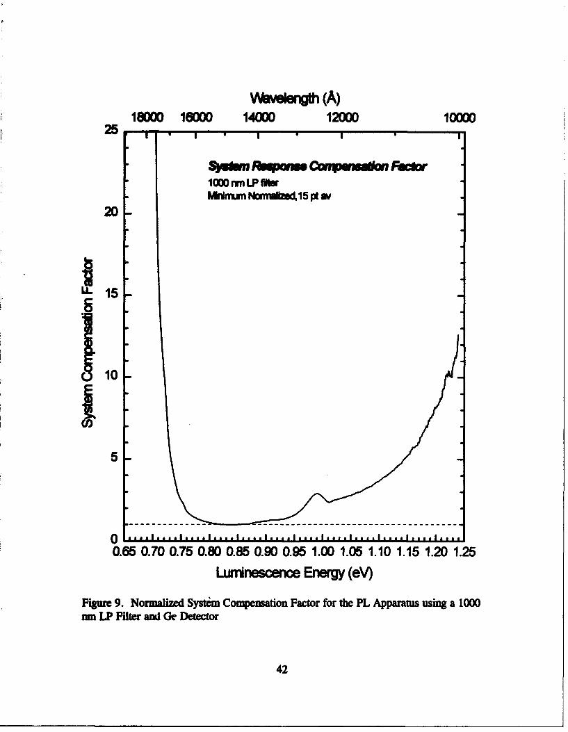
V~ve t (A)1000 16000 1400M 12000 10000
25 I
I=0 mn LP fitrMrimu Norfinu 15 pt av
20
U- 15
110
5
0 ,,,, I. ..hI . ..I ,,..l,.,.l,,,i ,.,.l .... lh~ppu.. .i.. illllI llll
0.65 0.70 0.75 0.80 0.85 0.90 0.95 1.00 1.05 1.10 1.15 1.20 1.25
Luninescence Energy (eV)
Figure 9. Normalized Systim Compensation Factor for the PL Apparatus using a 1000nm LP Filter and Ge Detector
42
blackbody. a flatiations have been smoothed using a 15 point smoothing
algorithm. To apply this, all of the intensity values of a PL spectrum would have to be
multiplied point by point (discretely) by this system compensation factor. In most
cases in this work, the absolute intensity of spectral lines is not important, and they
have not be compensated. The Pr emission lines of interest occur in the 0.75 through
0.80 eV and the 0.85 through 0.90 eV regions and have nearly the same response
factor, so compensation would accomplish little.
Error AaJylk. There are three major sources which contribute to energy
and/or intensity uncertainty in the PL experiment. These are 1) linewidths introduced
by the system, 2) finite data resolution, and 3) background variations. Each of these
effects influence the data in different ways.
A spectrometer will produce an output line having a finite width even if the
incoming light is perfectly monochromatic. This instrument linewidth is a measure of
how much the instrument smears or broadens the lines and is due to the finite optics
employed by the spectrometer. Specifically, this is mainly due to diffraction effects
including the resolving power of the grating and the width of the slit being used. The
grating linewidth AX, is defined as
AXg = X, (5)MN
where X is the wavelength of the light, m is the order of operation of the grating
(typically 1), and N is the number of grating lines. The linewidth due to the finite slit
of the spectrometer is
AX= acosOm (6)mf
43
where a is the slit width, 0. is the diffraction angle off the grating, m is the grating
order and f is the instrument focal length. Thus, the overall linewidth of the instrument
is AX = AXg+A&,. Typically, the slit width contribution to the overall linewidth is
dominant. The linewidth for a typical PL spectra in this study using the 3/4 m
spectrometer with 400 micron slit results in an 8 A or less linewidth for the Pr
emissions of interest. This equates to a maximum linewidth of 0.59 meV for the Pr
emissions found at 13000 A. Thus the very narrow RE emissions will appear to be at
least 0.59 meV wide and 2 lines separated by less than this energy will be very difficult
to distinguish.
Finite data resolution results from the periodic sampling of the luminescent
intensity by the data acquisition software. This periodic data sampling limits both the
accuracy that can be ascribed to a wavelength information and also the maximum
intensity of a peak. For example, using a 2 Hz sampling rate with the spectrometer
scanning at 400 A/min gives a data resolution of 3.33 A per data point. This serves as
the uncertainty assigned to wavelength positions throughout this study. In addition, the
finite data resolution limits the accuracy which can be ascribed to any peak's intensity
since the intensity sampling is unlikely to occur exactly at the peak. In fact, the worst
case data sampling event occurs when the sampling occurs exactly equally on either
side of the actual peak. This worst case can be quantified and used as the upper limit
for uncertainty of all peak intensities. In order to model this case, the shape of the
intensity peaks must be determined. There are two main optical mechanisms in the
s er which contribute to this: 1) the far-field diffraction effects of the slit and
the grating, and 2) the one-to-one slit imaging designed into the spectrometer. The far
field diffraction effects would cause a peak shape of sic 2 (Hecht and Zajac, 1979:343-
347,358-361), while the imaging of the slits produces a convolution of slit images and
44
wouldM pdce a trianie-shaped peak (Brfgel, 1962:123). In both cases, the width of
the modeled peak is determined by the theoretical FWHM of the slits since all RE
emission reported have istrunment-limited linewidths (which was confirmed by
examining high resolution spectra of the peaks). For a typical PL experimental run
using 400 micron slits with a scan rate of 400 A/min (a data resolution of
3.333 A/point), the worst case of peakjntensity uncertainty is 8.9% for the sinc2 model
and 18.9% for the triangle model. This analysis serves as assurance that reported
intensities in this study are accurate.
Finally, the actual intensity of lminescence also varies with the background
fluctuations which are inherent in any measurements using an electrical or optical
system. These fluctuations can be quantified by fitting a linear regression line to a
portion of spectra consisting only of background signal. An intensity measurement
may then be assigned an uncertainty equal to one standard error of this regression line.
S lZtve Ex eita i *
Selective excitation luminescence (SEL) differs from the PL technique in that
the energy used to excite the crystal is varied. The key difference is that in PL a single
excitation energy is used and a range of the output spectrum is scanned, while in SEL a
single wavelength output (like a rare earth emission line) is monitored while exciting
the sample over a range of energy values. Instead of greater-than-bandgap excitation
for simple PL, a tunable laser is used with which energy states in the sample are
selectively populated as the excitation energy is varied. The measured intensity of a
particular output line peaks whenever the excitation energy of the tunable laser
coincides with an energy transition intrinsic to the excitation of that particular
emission. The intensity may also fall, indicating that the laser has selectively activated
a competing transition mechanism. This method can then be used to determine
45

processe which ame rlaed to or compete with the excitation process by enhancing
ce transitions selectively.
In e etzo (em L), the excitation is provided by suppling potential
and/or kinetic energy to free carriers in the sample (Pankove, 1977:9). These fre
cariers then recombine producing light. For example, a p-n junction forward-biased
sufciny to alow propagation of electrons throughout the CB beyond the Junction
will asumne current injection mode (Figure 10) and those electrons will recombine with
holes on the p-side of the junction to produce light. The flow of CB electrons across
the junction (injection current 1) and the corresponding photon emissions increase
rapidly with the bias voltage V according to the diode equation (Pankove, 1977:180)
I = 10(e~ - i)l(7
where o is a current constant which is proportional to
•[-('-•}•],(8)
where E. is the bnigap, k is the Boltzmann constant, and T is the sample temperature.
The energy term 4 is the smaller of f or 4. for which E,+ is the barri which
electrons must overcome for injection into the p-type junction region and E,+4 is the
barrier for hole injection into the n-side (Figure 10). In this injection mode, direct and
indirect band-to-baz, recombinations become possible, along with the most of other
radiative and non-radiative transitions already mentioned. Alternate decay modes, such
as trapped.charge lumisc or Auger recombiations, compete with the desired
radiative transition and need to be minimized if possible.
46

44
Figure 10. Electron Injection. in a p-n Junc~tion (after Pankove, 1971:181)
As the in*eci diode as electrically pumped, many free carriers and excitons
are created. Hopefully, some of the jrecomnbination energy will be transferred to the
RE Mf energy levels with accompanying decay to produce techlogically desired
wavlenth. Since excitaton of rare earths in practical devices will probably be
ecwlusivey through electrical pumping (electroluminescence via carrier iqjection),
Of efficient electroluminescence is an important step in research leading
to fabrication, of devices.
47

VI. REI1UTS ANDDI•C,_ ¶QI
The rests con be grouped according to the objectives for this research effort.
The fiM studiies, which include examination of the Pr PL control sample runs,
a mg dependee, dose dependence, and doping dependence, am directed
pim Y toward ot-imization of the Pr emissions. The next series of studies including
hoat miaerai dependence, laser excitation power dependence, -e t -- dependence,
and excitation energy dependence aim at the heart of this effort; that being to
undersPnd the excitation mechanism of Pr in semiconductors. The codoping and dual-
doping efforts me attempts to enhance the Pr l through the use of
additional elements in the lattice. The last research study consists of fabrication of a Pr-
riased ft ies~lcent diode.
Pr Lnmin e Sdy of Control SMles
Verification that the emissions attributed to Pr are valid requires comparison of
samples with and without Pr. In this case, both implanted and unimplanted control
sample were identically prepared and annealed for each of the semi-insulathig (SI)
hosts. All AIxGalixAs hosts were MOCVD-grown on GaAs substrates, while the
SI-GaAs is LEC-grown. The LEC-grown GaAs was used because greater amounts of
material were available and tests showed that Pr emissions from LEC-grown and
MOCVD-grown GaAs were virtually identical. Figure 11 shows the low temperature
photoluminsence of each pair of samples for the SI-GaAs and SI-AIxGal-.As with
x=0.15, 0.30, and 0.50 hosts. Anneal temperatures are representative of significant Pr
emissions, although they are not optimal; this will be shown in the next section.
Although the emission itensities vary, in all cases the sharp line emissions in the two
ranges from 0.755-0.783 eV and 0.893-0.945 eV are evident only in the Pr implanted
48
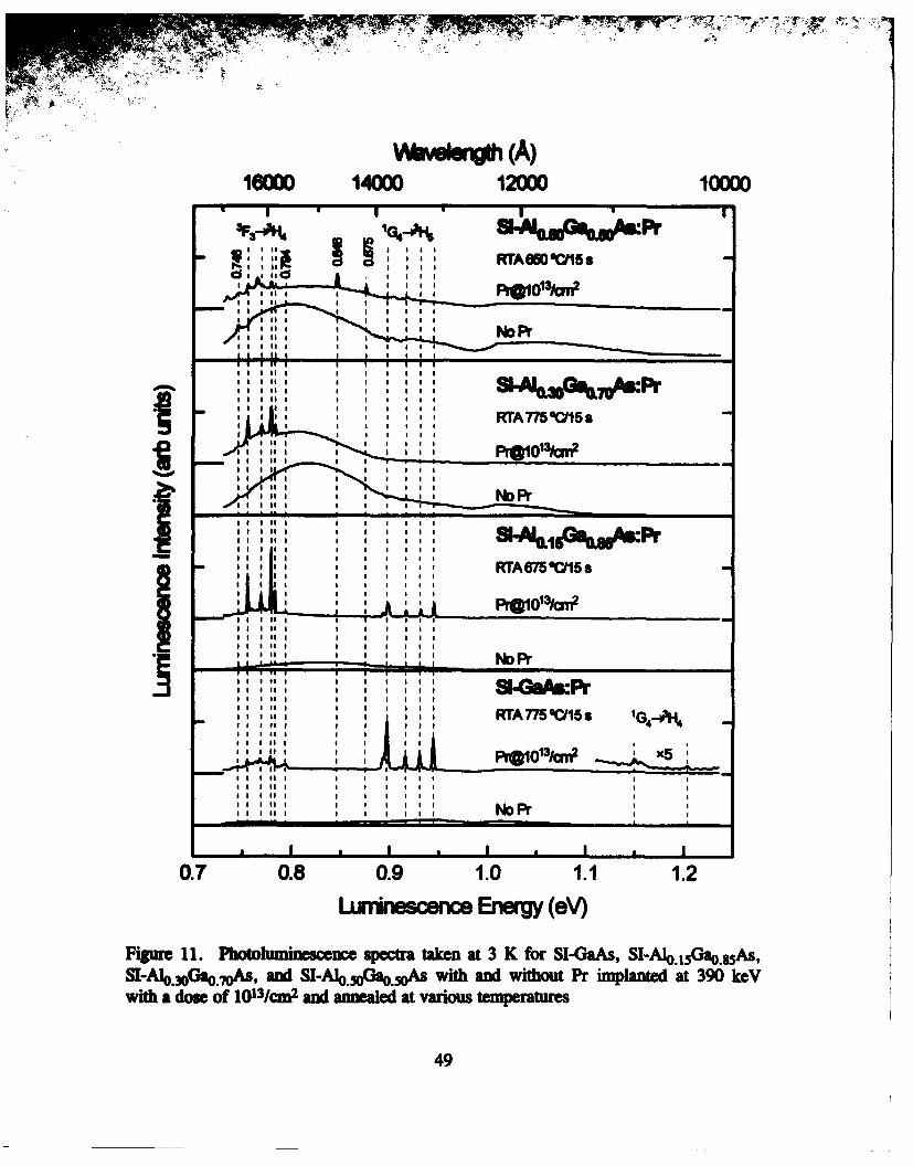
I I'
3F7f G4^ m~aojfp
RTA6SO C/15a
ND Pr ~ *~r
11 1 1I II I : oi
II til U I URTA7T5CII5s
IG4
II till I I I
0.7 0.8 0.9 1.0 1.1 1.2Lurrinescenc Energ (eV)
Figur 11. Photolu~misec spectra taken at 3 K for SI-GaAs, SI-AIo.Ciao~gAs,SI-AI0Ga0As,.M and SI-AIO.SGa.5As with ami without Pr implanted at 390 keVwith a dose Of 10)131CM 2 ami mmaled at variou epeaue
49
hosts and are thus attributed to Pr emissions. In addition, weak, sharp line emissions
are seen 1.150 and 1.204 eV in SI-GaAs:Pr only. All the emissions from the SI-
GaAs:Pr are the same as reported by Pomrenke et al. and the common energy positions
and emission strctures of each group provide evidence that the same transitions are
responible for the emissions in each host (Pomrenke et at., 1991b:418-419). No
phonon absorption-based replicas of the Pr emissions can be identified, implying that
these Pr-related transitions are not coupled to phonons in the host lattice. Phonon lines
are not expected, since the shielding of the Pr 4f electrons should prevent any direct
coupling to the lattice and this lends more evidence to the intra-4f level transition origin
of these emissions. These emissions are thus assigned to Pr3+ 4f transitions following
assignments first determined by Pomrenke et at. (Pomrenke et al., 1991b:418-419): the
0.75 eV group results from 3F3-+3H4 transitions, the 0.9 eV group results from
'G4-- 3H5 transitions, and the 1.150 and 1.204 eV emissions result from IG4-+3H4
transitions. Assuming no forbidden transitions, the highest energy peak in an emission
group results from a transition between the lowest state of the thermalized upper energy
level and the lowest crystal field split state of the termination level. Using this as a
guide, the lowest energy peak in these emission groups are offset from the Pr3+ free
ion energy level transitions (Table 3) by -4 meV for 3F3-- 3H4, -4 meV for IG4-- 3H5,
and +3 meV for IG4-- 3H4. This offset is due to the crystal field splitting of the free
ion levels into states with both higher and lower energies.
In order to determine the actual linewidth of these emissions, the full-width-at-
half-maximum (FWHM) was measured for several lines of the Pr emissions. All lines
in the Pr 3F3-+3H4 emission group were examined in the SI-Al0. 1sGao.ssAs host for
spectrometer slit widths ranging from 600 to 100 microns. All peaks showed a
smoothly decreasing FWHM, but below 100 microns the peaks were too weak to
measure. The strongest and narrowest is the 0.779 eV (15914 A) peak which exhibited
50

a P at .0*0. A/fr a 100 mkcm Alk. Thi corresponds to an upper bound of
0.294 =V for ft most nrow Pr emission l.ewidths.
1MW broad emisions visible in both impliamd and unimplanted samples
cealred rear 0.82 eV are due to unidentified impurity- or defect-related deep levels in
tde host mi. The very weak structure noticeable near 0.9 eV in these broad
anlasions is an artifact of the system response in that energy range. An emission line
at 0.746 eV was detected in all implanted and unimplanted samples, which must then
be host smiconductor-related. A small unknown emission line at 0.794 eV is seen
only in Pr-implanted SI-GaAs and SI-AI1Ga0.Aso. and it is not related to the Prr+
emissions. This conclusion was made based on the dissimilar behavior of this emission
line to Pr emissions. For example, the 0.794 eV peak decreases with increasing anneal
tmperatur (Figure 12), but increases with increasing dose (Figures 14 and 15) in
contrast to the behavior of Pr emissions. The emission lines at 0.846 and 0.875 eV are
detectable in the SI-Alo.I0Ga0.50As hosts only for RTA ttures less than 700 0C
and most likely emanate from unannealed ion implantation damage.
No direct evidence of the 3F4-- 3H4 transition was found implying that either
selection rules preclude this or, more likely, that the closeness of 3F3 and 3F4 allows a
strong path of non-radiative (Utrmalized) transitions from 3F4 to 3F3. Erickson et al.
noted that for levels with an energy difference of less than 4 phonons, the ion relaxes
via non-radiative phonon processes, while larger energy difference transitions produce
a photon (Erickson et al., 1993:2348). The 3F4-- 3F3 spacing is less than 2 GaAs
phonon energies and is thus consistent with this.
The strong emission groups have been identified with transitions to a lower state
of J = 4 and 5, respectively. As shown in Table 1, both of these J states have crystal
field splitings of 4 in cubic symmetry. However, the main emission groups have at
least 4 strong and several weaker sharp emission lines. This number of emission lines
51

then implies that the emissive Pr atoms occupy less than cubic symmevy, but no
specific site symmetry may be assigned since the exact number of energy level
splitings cannot be directly inferred simply from the nmmber of emission lines.
No Pr-relate emissions were detected from Pr implants in n- or p-type silicon
over a tested anneal range of 450-900 °C and doses of I X 1013 and 5 x 10¹³/cm2 . Only
emissions from the band-edge and near band-edge levels were found. This is attributed
to the comparatively narrow silicon bandgap (1.17 eV at 0 K) which is slightly lower
than the IG4 energy level in Pr and more than 0.3 eV from the next lower level (F 4)
causing an\energy mismatch of the exciton bound to Pr 3+ and any energy levels in
pr3 +.
Efec of AUnefing r-onditions on Pr I umi===.
Establishment of the RTA conditions which are most conducive to Pr
photoluminescence is a vital first step. This step serves the primary purpose of
creating a sample set with the maximum possible PL for each host. All annealing was
conducted using the RTA method at various temperatures for 15 second durations.
Hosts used were SI-GaAs and SI-AlxGal-,As with x=0.15, 0.30, and 0.50 implanted
with Pr at 390 keV with 1013/cm 2 doses.
Figure 12 shows the PL spectra obtained at 3 K from SI-GaAs:Pr. The zero
luminescence level of each spectrum is indicated by a short horizontal line on the left
axis. The emission spectra consist of two main emission groups: one based near
0.78 eV and the other near 0.94 eV. The former group consists of a series of small
peaks punctuated by 3 main peaks at 0.756, 0.769, and 0.779 eV, and are attributed to
intra4f transitions between crystal-field-split states of the excited level 3F3 and the
ground state 3H4 of Pr3 +. The latter group consists of at least 5 relatively strong peaks
at 0.893, 0.898, 0.917, 0.931, and 0.945 eV, and these are attributed to the transitions
52

1600 14000 12000 10000
PR GTO M #ýx1O1 io5
RT3 82 gal 5 s
0.7 0.8 0.9 1.0 1.1 1.2Lurniescence Energy (eV)
Fgur 12. Phmtohzminescence spectra taken at 3 K for SI-GaAs implanted with Pr at
390 keV with a dose Of 10131CM 2 and annealed at various tmeaue
53
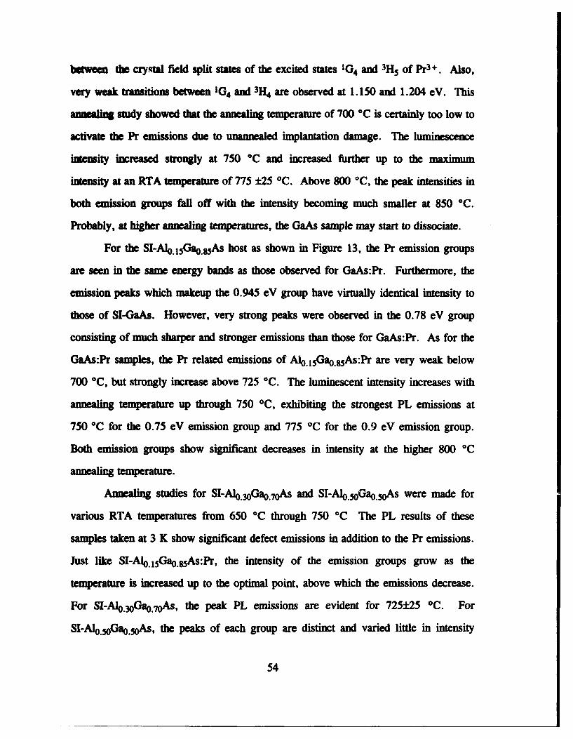
between the Cry~qal field split states of the excited states IG4 and 3H5 of Pr3+. Also,
very weak transitions between IG4 and 3H4 are observed at 1.150 and 1.204 eV. This
amwaft study showed that the annealing temperature of 700 -C is certainly too low to
activate the Pr emissions due to unannealed implantation damage. The luminescence
intensity increased strongly at 750 °C and increased further up to the maximum
intensity at an RTA temperature of 775 ±25 IC. Above 800 °C, the peak intensities in
both emission groups fall off with the intensity becoming much smaller at 850 *C.
Probably, at higher annealing temperatures, the GaAs sample may start to dissociate.
For the SI-Alo.IsGao.SSAs host as shown in Figure 13, the Pr emission groups
are seen in the same energy bands as those observed for GaAs:Pr. Furthermore, the
emission peaks which makeup the 0.945 eV group have virMaly identical intensity to
those of SI-GaAs. However, very strong peaks were observed in the 0.78 eV group
consisting of much sharper and stronger emissions than those for GaAs:Pr. As for the
GaAs:Pr samples, the Pr related emissions of Al0 .15 Gao.gsAs:Pr are very weak below
700 °C, but strongly increase above 725 °C. The luminescent intensity increases with
annealing temperature up through 750 °C, exhibiting the strongest PL emissions at
750 °C for the 0.75 eV emission group and 775 °C for the 0.9 eV emission group.
Both emission groups show significant decreases in intensity at the higher 800 *C
annealing temperature.
Annealing studies for SI-Al0.3oGao.7oAs and SI-Alo.oGao.5oAs were made for
various RTA temperatures from 650 °C through 750 -C The PL results of these
samples taken at 3 K show significant defect emissions in addition to the Pr emissions.
Just like SI-Al0.15Ga0.85As:Pr, the intensity of the emission groups grow as the
tem ature is increased up to the optimal point, above which the emissions decrease.
For SI-Alo.3oGao.7oAs, the peak PL emissions are evident for 725±25 OC. For
SI-Ao.5GaoAs, the peaks of each group are distinct and varied little in intensity
54
Waveength (A)16000 14000 12000 10000
3F3-AI 4 lG4-a.H PlO )E1 1%OlI IIII
POkeV, lxl01/kn-P'1'1T=3 KRTA 800C15 s
- .•_• - _•_ _RTA ,7O 0,U15s
S' ' 'RTA 650 V,1 5 s
I I IIi III I III I I
II I I I
S I I II -I -I I I
I I I" •-: •- LI_ . RTA770CJ15s
I I I
I I Ii I I I SI I I I
' ' ' 'RTA675OCJ15s
I I I I
I * I * I * I *
0.7 0.8 0.9 1.0 1.1 1.2
Luminescence Energy (eV)
Figure 13. Photoluminescence spectra taken at 3 K for SI-Alo. 15Gao.g5As implantedwith Pr at 390 keV with a dose of 1013/cm2 and annealed at various temperatures
55
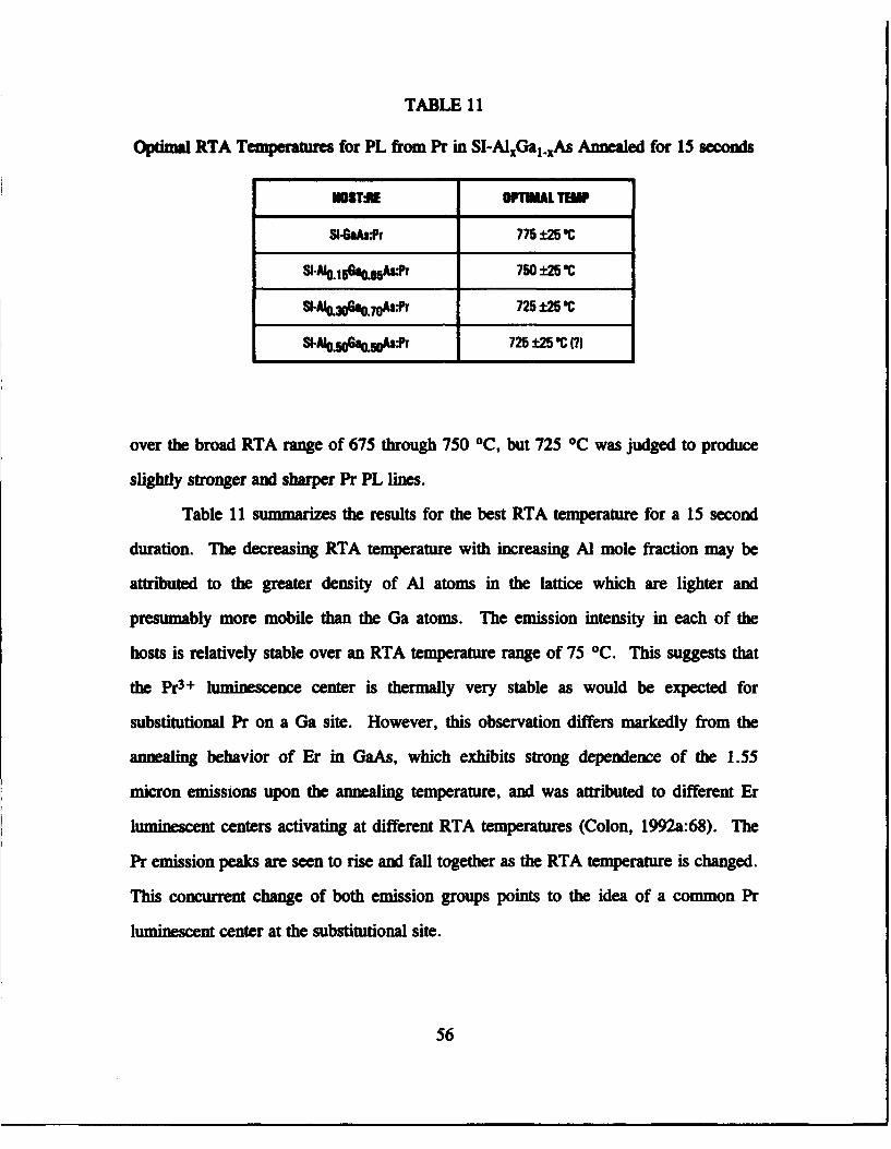
TABLE 11
Optimal RTA Temperatures for PL from Pr in SI-AlxGaI.xAs Annealed for 15 seconds
OSMTE OPIMAL TEMP
SIGaAsPr 775:t25 OC
sIA-0. 5Saogur 750 ±2 'C
%%.4 JOM70APr 725 ±25 'C
SA-•.8oao.soAs:Pr 725 ±25 'C 1?)
over the broad RTA range of 675 through 750 °C, but 725 °C was judged to produce
slightly stronger and sharper Pr PL lines.
Table 11 summarizes the results for the best RTA temperature for a 15 second
duration. The decreasing RTA temperature with increasing Al mole fraction may be
attributed to the greater density of Al atoms in the lattice which are lighter and
presumably more mobile than the Ga atoms. The emission intensity in each of the
hosts is relatively stable over an RTA temperature range of 75 °C. This suggests that
the Pr3+ luminescence center is thermally very stable as would be expected for
substitutional Pr on a Ga site. However, this observation differs markedly from the
annealing behavior of Er in GaAs, which exhibits strong dependence of the 1.55
micron emissions upon the annealing temperature, and was attributed to different Er
luminescent centers activating at different RTA temperatures (Colon, 1992a:68). The
Pr emission peaks are seen to rise and fall together as the RTA temperature is changed.
This concurrent change of both emission groups points to the idea of a common Pr
luminescent center at the substitutional site.
56
apaing the RE dose may either increase or decrease the RE luminescence.
Higher doses do introduce more potentially luminescent centers, however,
accompanying the greater RE density is the problem of solubility limits. Above the
solubility limit, impurities form precipitates which cause major lattice defects due to
the volume mismatch. Exceeding this solubility limit has been shown to extinguish RE
PL. For example, Favennec and coworkers saw a decrease in GaAs:Er PL for very
high Er doses and attributed this to absorption from unannealed implant damage
(Favennec et at., 1989:333). The Er solubility limit was quantified to be about
7 x10¹⁷/cc, where, above this limit, Er forms near spherical microparticles of ErAs
which are not luminescent (Poole et al., 1992:121). However, Langer et al. reported
that Er-related PL in MOCVD-grown GaAs:Er was a maximum at an Er concentration
of 1.2 x 10¹⁹/cc (Langer et al., 1993:15). Higher implantation doses may also decrease
the luminescence because of increased lattice damage. The defects in an amorphous
lattice can trap free carriers where they will non-radiatively recombine through a
continuum of states (Pankove, 1971:165), thus robbing the RE of luminescence fuel in
the form of free carriers and excitons.
The purpose of this study is to determine the optimal implantation dosage for
PL in each host material and to estimate the solubility limit of Pr impurity
concentration in the host lattice. The doses used were 5x10¹², 1X10¹³, and
5 X 10¹³/cm2 in each of the optimally annealed SI-hosts used in the RTA study. Figures
14, 15, 16, and 17 show the low temperature PL spectra of Pr at these doses in hosts of
SI-GaAs, SI-AI0.15Gaos85As, SI-Al.3Gao~oAs, and SI-Al.5GaoAs, respectively.
The SI-GaAs case shown in Figure 14 is interesting because the optimal dose is
different for the two emission groups. The strongest 'G4-+3H5 emissions were
observed from the sample with a dose of 1 X 10¹³/cm2, while the 3F3-- 3H4 group
57

VWve~eflth (A)16000 14000 12000 10000
I "I 1 "
SRTA 775 C015 9, T=3 K
, ,•, L•PrO xl°3/CMn2 ,G41
a aa a
a aa !
prtVX1OI 3Icnf G4 3H
0.7 0.8 0.9 1.0 1.1 1.2
Lurnneswr= Errg (eV)Figure 14. Phatoluminescence spectra taken at 3 K for SI-iaAs implanted with Pr at390 keV with a dose of 5 x 10¹², 1 X 10¹³, or 5 X lO131Cn2 and annealed at 775 °C
58

W&AW Vh (A)16000 14000 12000 10000
3F^ 84ya -rm.-DA&Pr
I• I " I I I"
I,' Pro=0 koy' REA 775 0C015 s, T =3 K
I• i G4-3N 'G4-
l Pr•1x10131CMl
II n I .I . I , I
0.7 0.8 0.9 1.0 1.1 1.2
Lrinume em EneW (eV)
Figure 15. Photoluminescence spectra taken at 3 K for SI-Alo.jsGao.g5As implantedwith Pr at 390 keV with a dose of 5 × 10¹², 1 X 10¹³, or 5 X 10131Cn2 and annealed at775 °C
59
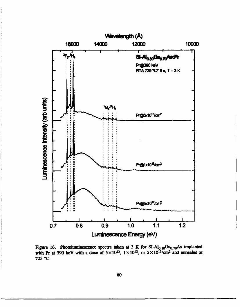
1l000 14000 12000 10000
3 VFL *I O AI
RTA 725C15$, T=3K
Is *
* ,* .
Ir3
I|,,,pW~dOI3/Crr
* e
m fI I I
0.7 0.8 0.9 1.0 1.1 1.2
Lminescenre En&W, (eV)
Figure 16. p~ztoolumnsec spectra taken at 3 K for SI-Alo.3oGao.7oAS implanted.wit Pr at 390 keV with a dose of 5 x 10¹², 1 X 10¹³, or 5 X 10¹³/CM2 and annealed at
725 °C
60II
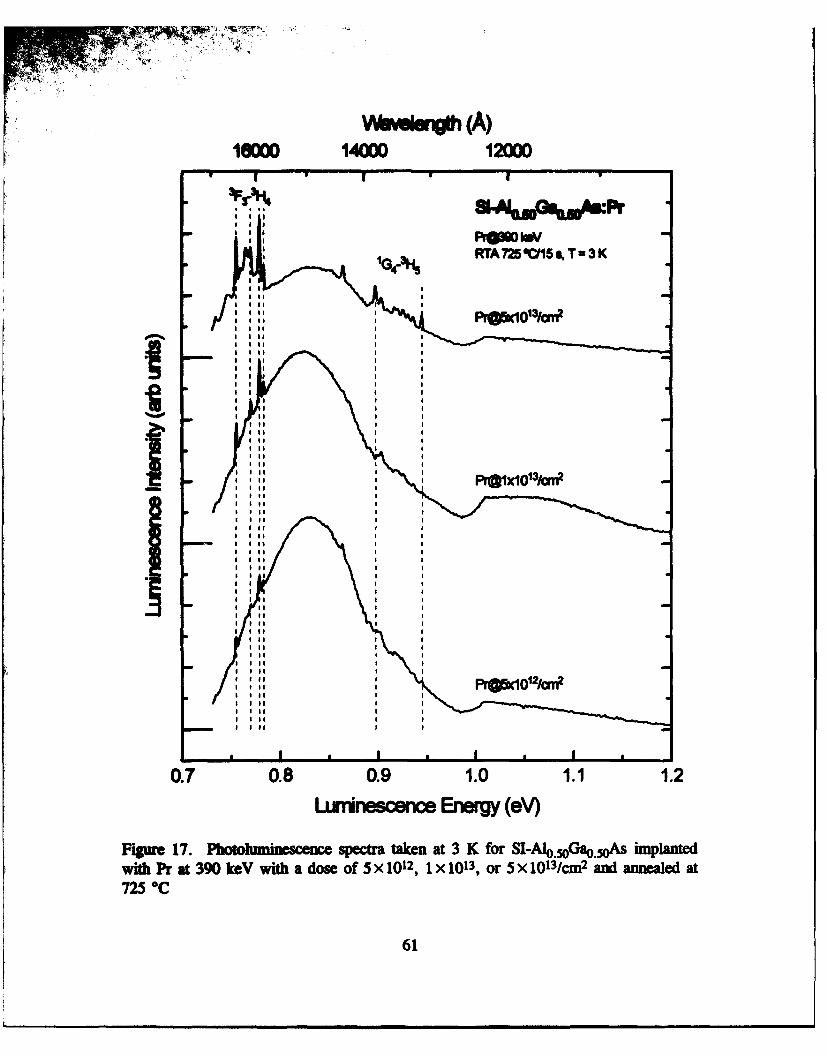
V~bw~sri- (A)
0.700. 0.9 1.00 110.
RT720C5C=3
61o1kr

TABLE 12
Opehnal Pr Dose for PL from Pr in SI-Al 1Gal.,As
MuthPr t F kIm
1x 10¹¹ G3-*3H)
~SM.10LMAI* 0.%5.,1013
S410,g7A~dr 501013
oo,*5o.ft5OA3:F 5.o1013
intensity inreased with dose. The middle dose was chosen for use in subsequent
experiments, since this results in the strongest arid sharpest peaks in the IG4-• 3 H5
emission group. For the SI-Alo.i o.85As host, the PL intensities of Pr emissions
were about the same for the two lower doses (Figure 15), however, the lowest dose
gave a slightly higher PL in both groups, and was chosen as the best dose. The
SI-Ao.3oGo.7As host shown in Figure 16 along with the SI-Alo.5oGao.(oAs host shown
in Figure 17 displayed 3F3-- 3H4 emissions which increased with dose. Both spectra
also show a broad defect-related emission centered around 0.82 eV, which decreases
with inreasing Pr dose. This can be explained if Pr and the defect center compete for
the same energy source presumed to be free excitons or carriers. Thus, the increased
Pr luminescence robs the defect centers of their pumping source. Alternatively, as the
Pr concentration increases, the recombination energy of the defect-related center may
transfer its energy more effectively to Pr3+ ions nonradiatively.
Table 12 summarizes the optimum Pr dose determined for each of the tested
hosts based on the strongest PL peaks, although a limited number of dose variants was
used. Since the implant profile is a Gaussian, the homogeneous concentration
62

by VIm* cm wt be dMeaued. Hevnw, for P , e-1 n p a the peakau
I. (3musia kh" profile was comuled using Eq (3) and Table 8. They are
cakulamd to be l3 x 1011cc for the 0.5 x 101//cm2 dose, 6 x 10¹⁸/cc for the I x 10 3/cm2
dowe, and 3 x I019/cc for the 5 x 10¹³/cm2 dose.
Pa b -• --- on the Host CgOnd•-titv M
The purpose of this study is to examine the effect of host carrier-type dopants
on Pr photo s . Semiconductors are routinely doped with impurities to alter
the type and concentraon of mobile carriers in order to control their electrical
characteristics. In addition, RE luminescence has been shown to depend on free
carriers (as excitons). Dopant elements are chosen to have valence characteristics
different from those of the host in order to add free carriers (either electrons or holes).
These free carriers can absorb recombination energy of free excitons via an Auger
process, thus robbing the RE's pumping energy.
For this study, MOCVD-grown GaAs and Alxal..xAs hosts of x=0.15, 0.30,
and 0.50 were available in SI-, n-, and p-type versions and were identically implanted
with Pr. Samples were then annealed at the optimal temperatures determined for each
host. Low temperature PL spectra from each variant were then examined to determine
the effect of carrier-type doping of hosts. The impurities were Si for the n-types and
Zn for the p-types which were doped during the MOCVD growth process. The vendor
Epitroncs reports that carrier concentrations in both were 1.0 I017/cc.
Figure 18 shows that the Pr PL is much stronger for the SI-type Al. scGao0.As
host than either the n- or p-type variants. Both emission groups suffer strong
reductions in intensity with the addition of either n- or p-type dopants. Similar results
were also observed for Pr PL in the Alo.3oGao.70As host. This probably represents an
effect similar to that found in the dose dependence (Figure 16), where the Pr competes
63
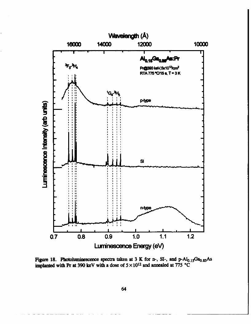
V~veen~h(A)16000 14000 12000 10000
' I * I * I 1
AP,9O e%,cOft~
RTA775 C1I5 s, T= 3K
1S1
L~sirw4w=ErW (V
II I
ipatdwtPrat 39 a Vwt a dos of 5a 02a nna t75
a 64
a a|a i a i a
a aa aI| aa a|| a a
a a a
a aa a I a
aii a
Fiue 8 Poolmmse• pctatae a Kfra-aS- adSIolsa~s~
imlnedwt ar iat 39 Vwt a dos af5x11 n nn.f t75°
wit odn impurity or defect-relatd centers for the pumping energy of
ctmarriers or deactivation of Pr PL via non-emissive complexes formed with the
extra impurities. Figure 18 supports the former theory, since strong defect emissions
are evident in the doped hosts at 0.77 and 1.15 eV. This effect, in which donors and
accptors act as "shunt" recombination centers, has been noted by others studying REs
(Lozykowski, 1993:17761). If this effect is dominant in moderate- to heavily-doped
electrohuninescent devices, Pr luminescence may be weak or non-existant due to this
apparent inability to compete successfully against other impurities for the supply of free
carriers or excitons.
A different PL result was found for the conductivity-type dependance of GaAs
and Aio.5oGa0.5As host as shown in Figures 19 and 20 respectively. These hosts
showed increased Pr PL for both n-type and p-type doping than PL for undoped
materials. The exception was the n-type GaAs which displayed a very strong, broad
defect spanning 0.75 through 1.15 eV (Figure 19). The Pr lines were apparently
completely quenched by the effects of this defect-related peak. The apparent n-type
host peak at 1.0 eV is an artifact of the experimental system response and water
absorption lines can be seen between 0.8 and 0.9 eV. Otherwise in these two hosts,
the two main Pr emissions groups showed an increase in intensity of several times
compared to the SI-type host.
Pr L-uminescen ~c ednce on Host Seiconductor
Investigating the effects of changing the host semiconductor can reveal
dependence of the Pr PL on controllable factors. In this study, the Al mole fraction x
in SI-AlxGaI.xAs hosts was varied from 0 to 0.50. There are 3 major effects of the Al
on the host which may affect Pr luminescence. These are 1) the increase in the
bandgap with increasing aluminum fraction, 2) the alteration of the crystal field and
65

16000 14000 12000 10000• I " I
i ~Pr iVlonm
RTA775'/15s, T:=3K
II
I I
0.7 0.8 0.9 1.0 1.1 1.2Luninescenc Energ (eV)
Figure 19. Phoftolminiescence spectra taken at 3 K for n-, SI-, and p-GaAs implantedwith Pr at 390OkoV with adose of IX 1013 and annealed at 775 0C
66
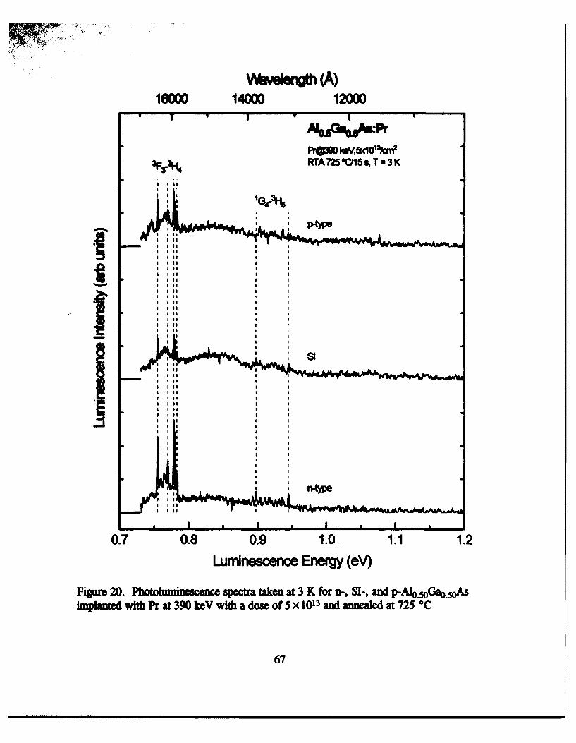
V~e~rio (A)1000 140002 12000
PrGO kdU,&1Ol 3JAMnI3F,.3NRTA725*Cd15T=3K
I
I
I
In I
0. 0.8 0. 1. . .
Iuimsm IIg (eV
Fiu 20. PhthInsec spcr ikna3Kfo - lndpA.5a.q&
Imlne with Pra 9Ie ihads f5X11 daae t75*
I III67
symmetry hnduced by the Al atoms, and 3) formation of AI-Pr complexes. For these
hosts, the low temperature direct bandgaps are 1.519 eV (x=O), 1.733 eV (x=O.15),
and 1.940 eV (x=0.30) (El AMli et a., 1993:4403), while the x=0.50 case produces
an indirect bandgap of about 2.07 eV (Alferov et al., 1973:1622). Wider bandgaps
create higher energy free excitons and span greater energy levels in the Pr ions,
potentially producing a more diverse set of intra-4f transitions. Alteration of the
crystal field and symmetry due to the presence of Al atoms in the lattice reduces the
symmetry thus increasing the number of crystal field split states of all free ion energy
levels. Increasing the aggregate levels available for transitions is likely to increase the
number of emission lines, but concurrently may decrease the intensities. Finally, the
presence of Al atoms in an otherwise GaAs lattice may be considered to be high density
impurities which can form binary complexes with the Pr ions. Not enough is
understood about RE-impurity complexes to predict whether the Pr luminescence from
such a complex would be greater or lesser than that from an 'isolated' Pr ion.
In this study, Pr was implanted at 390 keV with a dose of 1 x 10¹³/cm 2 in hosts
consisting of SI-GaAs and SI-Al1 Gal-..As with x=0.15, 0.30, and 0.50. Annealing
was conducted using the optimal temperature for each host. Low temperature PL data
was collected on each sample under otherwise identical conditions.
It was found that changing the Al fraction in the hosts had a dramatic effect on
the Pr luminescence as shown in Figure 21. While the 0.9 eV emission group is
dominant in the PL from GaAs hosts, the 0.75 eV group is strongly dominant in all Al-
bearing hosts with xŽ0.15 and appears to be quite abrupt. In GaAs, the IG4-+3H5 Pr
emission group intensity dominates that of the weak 3F3-+3H4 emission group. In
Al 1o 5 Gao.85As, this behavior is reversed with the 3F3-+3H4 Pr emission group showing
much stronger intensity than that of IG4-- 3H5 , which has intensity and peak profiles
almost identical to those of GaAs:Pr. As the Al mole fraction in the host increases to
68

Waveength (A)1700160 15000 14000 13000
3F3-A-4p~ow kdv 1o13 rt2, T =3 K
A (P x--050, RTA 720C'4Zk
MNIxI O 30 Ir 72 OC
xIO 15 RT 775 O
1: IF .0 RT M I I
0.7 0.7 0.8 1.8 0.9 0.50
I u~rem Img (eV)I
Fiue2.poouinecesetatkna 3 K fo IGas SI-.5%.As
II43C%7~,E SI-45GOA imlne wtPra39 ewitadoef
I03/M aW IMae at vaiu emeaue
I I I 69

0.30, and 0.50, the still dominant 3F3-- 3H4 Pr emission group is significantly reduced
and the IG4-+3 H5 group is almost undetectable. Clearly the Al somehow causes
preferential de-excitation of the Pr through the 3F3-- 3H4 transitions, but this effect does
not follow the Al density in general since higher Al mole fractions reduce the absolute
intensity.
Figure 21 also shows the consistent position of the emission lines across all
hosts. To simplify reference to these many separate Pr emission lines, each of the
main peaks was assigned a designator based on very close energy positions across all
hosts and relative peak intensities within the emission groups. These letter designators
are shown above their assigned peaks in Figure 21 and these energy assignments are
summarized in Table 13 along with other strong lines. Table 13 lists the most exact
position of each emission line determined in this study along with hot lines (shown in
italics), which will be discussed in a later section on temperature behavior of the Pr
PL. The emission lines labeled U and V are very weak (see Figure 11), but clearly
visible in GaAs while U is only barely detectable in Al0 .15Ga0.g5As:Pr and not seen at
all in Alo.3oGao.7oAs:Pr or Alo.5oGa..5As:Pr. In only Al-bearing samples an additional
peak occurs at 0.778 eV (CO), which is not seen in GaAs hosts. This CO peak is very
near the C peak seen in all hosts and probably results from increased crystal field
splitting of the energy levels due to the lower symmetry in AlxiGalxAs compared to
GaAs. The nearly identical energy positions and relative intensities of the remaining
peaks within Pr emission groups in all hosts strongly implies that the Pr center
responsible for luminescence is on the cation site. Only Ga or Al sites preserve local
symmetry across all AIGaAs hosts because all four nearest neighbors are arsenic in all
hosts. A centered interstitial position of a Pr 3+ ion in Td symmetry would likely
include varying numbers of Al atoms as nearest neighbors. The average number of
these neighboring Al atoms will increase with Al mole fraction, thus increasingly
70

TABLE 13
Main pr3+ PL Emission Lines in SI-Al1Gal-.,As
Pr7 Energy Transition Peak, Host (eV±0.0002)
OMaio Trmsiion GIAstLEC Al0.15Gafs Al.3Gafs AO.oGaMs WaWn (INn)
A 3F3 .- 3H4 0.7557 0.7555 0.7555 0.7554,68 1.64
B 3F3 -.3H4 0.7688 0.7688 0.7693 0.7698 (?) 1.61
HLI 3F3-+-3H4 0.7723 0.7726 0.7728HLIa 3 F3 -. 3 H4 0.7750 0.7752
CO 3F3-+3H4 0.7785 0.7786 0.7787
C 3 F3 -+3 H4 0.7793 0.7794 0.7794 0.7795 1.59
D 3F3 .-+3H4 0.7830 0.7833 0.7834 0.7830 1.58
HL2 3F3-03-4 0.7893 0.7894
M 1G4-+3 H5 0.8933.36 0.8932 ? 1.39
HL3 1G4 -+3 H5 0.8942 0.8945
N... 1G4-+3H5 0.8976 0.8977,88 0.8977 0.8974 1.38
0 1G4-- 3 H5 0.9166 0.9169 0.9165 ? 1.35
P 1G4-+3H5 0.9315 0.9320 0.9311 (?) ? 1.33
HL4 1G4 -+3 H5 0.9342
Q 1G4-, 3H5 0.9453 0.9455 0.9451 0.9452 1.31
U 1G4 -+3 H4 1.150 1.15 1.08V 1G4 -+3H4 1.204 1.03
distorting the local symmetry around As sites or interstitials, but not Ga or Al sites.
This increased distortion should be manifest as increased numbers of crystal field split
states with an accompanying incr, ase in the number of PL transitions. This is simply
not seen as the PL peaks are very consistent in energy position and group profile across
the AlxGai..xAs hosts. This is further evidence that luminescent Pr occupies a
substitutional position in the host on the Al or Ga sites.
The assignment of these PL transitions to the states of specific levels allows
construction of an energy level diagram for the Pr3+ ion in AlxGa1.xAs. This diagram
71
is based on the common strong emissions identified in all hosts and depends on the
a i that low temperature do-excitation starts at the lowest state of the excited
upper level. That is, after excitation to some arbitrary state in an upper level, the
electron thermalizes to the lowest state in the level before making a radiative transition
to any of the manifold of the crystal field split lower level states. Figure 22 shows the
energy structure of those Pr3+ ion levels attributed to PL transitions observed in this
study. Due to the weakness of all emissions in the higher Al mole fraction hosts, not
all transition peaks can be identified, but emission peak energies and crystal field split
widths are common throughout the series. The apparent full width of the crystal field
split 3H4 level is 28 meV with 3 to 5 identifiable peaks, while that of the 3H5 level is
52 meV with 5 or fewer identifiable peaks.
Some previous reports provide instructive comparisons to these results. As was
already noted and expected, the GaAs:Pr PL is virtually identical to that reported by
Pomrenke et al. (Pomrenke et al., 1991b:418-419) and Erickson et a. (Erickson et al.,
1993:2348). Although Er emissions display the same consistency of emission line
energies independent of Al mole fraction in AlGaAs, the intensity increases with Al
mole fraction at least from x=0.l through x=0.4 (Colon, 1992a:66-68). Colon
attributed this Er PL behavior to either formation of optically active Al-Er complexes
or reduced thermal quenching as a by-product of the increased host bandgap. Thulium
also exhibits stronger PL intensity in AlGaAs than GaAs (Pomrenke et al., 1992:1925).
The evidence from this limited number of Al mole fraction samples is
augmented by parallel behavior from older samples of AlGaAs which provide not only
corroboration, but expanded information on the Al mole fraction behavior of the Pr
emissions. SI-Al0.1oGao.9 As and SI-Alo.20Gao.oAs wafers were implanted with Pr at
390 keV with a dose of 1 X 10¹³/cm2 and annealed at 750 OC for 15 seconds. The Pr
emissions displayed in Figure 23 for the x=0.10 sample are very similar to those of the
72
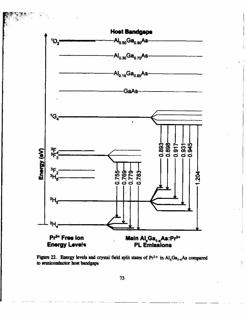
Host BngD 2 --~AIO.GaO5As-
Al0 3OGaO.7As
Al0.15Ga0.8As
Ga s
3 0OC 0) V-)*
1- 3
Pr"~ ~~ W Fr I%- ManGoG 1A:r
3H73

V*vedength (A)17000 1M00 15000 14000 13000
RTA75OI5s,T=3K
3F-A
x--0.20
X=0.10
0.7 0.5 08 .5 0 I .5 10
Luriwmo Iw IO
Rpr 2. Potlluinscecespetr taenat Kfo SI-Aol~og n
Alo20ao.~simlanedwih P a 30 kV it a os o I X 103I, ndanae
at 7I I II7

Ga"s u*Own earier With the 1G4-+3HS group intensity dominatig the 3F3 -+3H4 goup,
while the x=0.20 sample shows the opposite behavior. Although the x=0.20 sample
spectra displays a broad defect emission near 0.92 eV and water absorption between
0.87 and 0.93 eV, the 3F3-- 3H4 group of Pr3+ dominates the much weaker IG4-+3H5
group which is characteristic of samples with Al mole fractions greater than 0.15. The
Pr emission intensity behavior of these samples shows that the switch to stronger
3F3-- 3H4 emissions occurs at an Al mole fraction above x=0.10. Combining this with
earlier data, the Al mole fraction at which the Pr emission group intensity switch
occurs is between x=0.10 and 0.15. This behavior also presents further evidence
against Al atoms themselves as the cause for the intensity shift in Pr emission groups.
Pr T Ani Dtnee on Excitation Power
Determination of the behavior of Pr luminescence as a function of laser
pumping power is a requirement to guarantee the reliability and consistency of results
and can yield information on ttc -'xcitation process as well. It is important to keep
sample heating to a minimum, since the concurrent expansion of the lattice can alter the
experimental results. Operation of the laser at a power below saturation of the Pr
luminescence is desirable to minimize the effects of laser-induced sample heating. The
PL intensity variance with laser power for the 0.779 eV peak of SI-Al0.15Gao.85As:Pr is
shown in Figure 24. This is representative of the behavior of all lines in all hosts.
Three different laser apertures were required since no one aperture value can span the
entire range of power. As seen, operation of the laser in the 100 to 300 mW range,
which was used in all experiments in this effort, is well below any conceivable
saturation point.
No saturation power point for the Pr PL was detected in this study. No power
above 700 mW was attempted because of possible sample damage, but the steadily
75

30
2828oAI~G.sPr .L779 eV Peak25 - P Msv, 5•x1o%2 a
RTA 775c"15.24 -T=3K 0O
122
f20 8180
~16-0
~14 7
10 0
6-o-D-ApertmI#1
4 -o-Apeture#22 -0- Aerre #3
0 , a I .I , I , I ,
100 200 300 400 500 600 700
Laser Output PoWer (mW±5)
Figure 24. Behavior of the 0.779 eV peak of SI-Alo. 1 5Gao.85As:Pr with Ar+ laser
power
76

htreauinq iunteiy with power through 700 mW can be explained by paraleling the
woa of Benyattou et a. (Benyattou et at., 1991:2133). These workers found a square
root dependence of the PL intensity with laser power for the 1.54 p emissions from
Alo.55GaO.43As:Er. Their explanation assumed the Er introduced an isoelectronic trap
in the host bandgap which trapped excitons. The bound exciton recombination energy
could then be transferred either to the Er atom or to a free carrier via an Auger
process. The probability of this competing Auger process is then proportional to the
density of free carriers. Defining the concentration of free carriers as n, then the
likelihdod of the bound exciton recombination energy transfer to a free carrier is Bn,
where B is the transfer constant. The total probability for bound exciton energy
transfer to the Er atom is given by (Benyattou et al., 1991:2133)
PB (9)P, + Bn"
where P, is the excitation rate of the Er atoms. The rate equation for Er excitation is
then
dnk =A+ P. n, (10)dt P, + Bn T f
where n*, is the excited erbium concentration, A* is the concentration of bound
excitons proportional to the light flux *, and rf is the Er fluorescence decay time
constant. These workers further assumed a bimolecular recombination of the
photogenerated carriers requiring that n-B'(*)'12 and that the Auger process dominates
due to high flux rate. The steady state solution is then
77
A P , (01)n. = C
whom C-AE '. Thus the density of excited Er atoms, under these asumption, is
poportional to the square root of the pump power. This model can also be used to
explan the behavior of the Pr intensity. The Pr PL inmtensities I in Figure 24 were fit
to the equation
I= a + b4f-P, (12)
where P is the laser pump power in milliwatts and a and b are the fitting parameters.
A very good fit was obtained using a=3.64±0.21 and b=0.84±0.02 for the aperture
I case, a=3.88±0.13 and b=0.75±0.01 for the aperture 2 case, and a=3.74±0.45
and b=0.75±0.02 for the aperture 3 case. The use of the simple offset parameter a
was required for good fits and is justified as a correction factor corresponding to some
background luminescence at this peak. The behavior of the Pr luminescence with laser
power is well explained by this process showing that there is a substantial competition
for the BE recombination energy between the Pr ions and Auger processes of free
carriers.
Tempmramre D•ne of Pr lQnminLwP
In order to learn more about the nature of the Pr excitation mechanism, certain
paramters of the photoluminescence experiment may be altered while examining the
behavior of the Pr luminescence. One important parameter is the sample temperature.
While the analysis of PL emission lines alone gives the transition energies,
investigation of the temperature dependent changes in the PL spectra can give
important information such as:
78
F?' 1) o anbd amw k• shuctm via 'o lines,'
2) the ativation energies associated with the transitio corresponding to eachsperal line or group, and
3) identiftcation of different luminescent centers via distinct temperaturedependent behavior of emission lines.
The expanded energy levels are determined through the rise of 'hot lines.'
These are spectral lines not generally seen at very low temperature (< 3 K), but which
appear and grow as the temperature increases while the normal 'cold lines' are
diminishing. Hot lines result from the thermal populating of higher than the lowest
energy states in the upper level of an emissive transition. The energy state of the upper
level can be assigned by assuming that the next lowest spectral line transitions to the
same lower state or by using consistency between several hot lines.
The activation energy is more closely related to the excitation mechanism itself.
The activation energy represents an energy step in the excitation mechanism
responsible for the spectral line transition which is thermally deactivated as the
temperature increases. This effect is manifest as the familiar decrease in cold line
luminescence intensity as temperature increases. An example of a thermal
depopulation mechanism is excitons bound to shallow impurity energy levels. As the
�emprature increases, the bound exciton eventually gains sufficient energy to break
free from the impurity (dissociation). This temperature corresponds to the activation
energy via the Boltzmann distribution. Another mechanism which thermally
depopulates and is a plausible step in RE luminescence is electrons (or holes) bound to
imp (such as REs). These trapped carriers can form bound excitons and so
represent another path to excitation. The activation energy in this case corresponds to
the bound carrier ionization energy. Experimentally, luminescence which depends on
bound exciton recombination at an impurity site would diminish substantially above this
79
temperfaure. By their very nature, hot lines also reduce the intensity of their
accompanying emission group cold lines by decreasing the population of the lowest
energy state in the upper transition level. The hot lines will then have an activation
energy which will probably be different for each emission group since the crystal field
splittings are probably not identically spaced.
Paralleling Bimberg et al. (Bimberg et al., 1971:3451-3455), the activation
energy (or energies) may be calculated by assuming a Boltzmann distribution for the
exciton energy levels with c(o designated as the bound ground state and el as the single
excited or dissociative energy state. (Note that there is no inconsistency in viewing the
excitons or carriers in a PL-driven system as being in thermal equilibrium as distinct
from the steady state excitation/de-excition processes. The only requirement which the
excitons must meet is lifetimes sufficient for thermalization to equilibrium.) One next
assumes a fixed total number of excitons NG(J) at a temperature T with No(7) as the
average number of bound excitons at T and NI(1) as the number of dissociated
excitons. The conservation equation for this simple 2 level system is then given by
No(T) + N1(T) = NG(T). (13)
The ratio of the Boltzmann distributed particles in energy levels &o and el is
N1(T) = g , e-(e,-o)IkT, (14)
N0 (T) go
where gl and go are the degeneracies of the respective energy levels and k is
Boltzmann's constant. Identical equations hold for the ratios of the populations of
other energy levels if they are postulated. Combining these equations and assuming
only 2 levels, the ground state co and the dissociative energy state el, we obtain
80

NG(7) = N,(T)(l + g-es%) (5
The tmperature dependence of NO(M) is not known and is taken to be a constant over
the limitd temperature range of interest. Actually, this assumption is valid for PL in
which a constant laser power creates a constant density of eletron-hole pairs forming
excitons in the sample. This means that NG =NG(O)=No(O), so that
N°(T) = (I+cie-1/kr )I (16)
where cf=glgo and E1 =cf-fc. NO(1)ING(7) is thus the fractional number of excitons
still bound and therefore available for the radiative recombination process. Thus the
intensity of luminescence coupled to these bound excitons is proportional to the ground
state population as a function of temperature is
IT= N°(T) = (I +ce•/kT)-, (17)I0 NG (O)
where IT is the luminescent intensity at temperature T and I0 is the intensity at 0 K.
Thus this equation relates the temperature dependence of the spectral line intensity to
the activation energy El. The relative magnitude of the exponential coefficients
represent the efficiency of the quenching mechaninm corresponding to that activation
energy.
Double activation energies are typically used in activation energy calculations
for Er (Langer ata!., 1993, 19) and Yb (Tbonke et at., 1990:1128). These systems
are considered to represent a three state process. Paralleling the previous derivation,
81

the behavior of the PL imoenity resulting from a system with 2 activation energies is
LT (1 + cie-E'-T + c(e1-E')-,8)10
where E, and E2 are the activation energies and c1 and c2 are the corresponding
- facboro.
In practice, one records the integrated intensity of a specific peak at several
tempe�rat s and fits the data to Eq (17) or Eq (18) using /41 /o and T as the
I "depnt variables with c1 and E1 (and c2 and E2) as the dependent variables.
Computer programs such as Jandel's TableCurve can automatically find the best fit of
the data to the exponential activation energy equation.
The primary thermal quenching mechanism which may be manifest as the
activation energy for RE luminescence quenching is bound excitons dissociating from
the Pr ion to free exciton states. This process deprives Pr ions of their localized energy
source, thus quenching the luminescence. The actual energy Ex of a free exciton is
based on a hydrogen-like model with the electron-hole pair orbiting their center of mass
and is given by
Ex= -m'q 4 12Eh2 2 n2 , (19)
where mr* is the reduced mass of the electron and hole effective masses in the host, q is
the unit charge, h is Planck's constant (here reduced by 27r), 6 is the host
semiconductor dielectric constant, and n is an integer 21 indicating exciton excited
states (Pankove, 1971:12). Thus, the free excitons in a semiconductor have energies
dependent on the host hole and electron effective masses and the material's dielectric
constant. For Al.Gai. 1As, these energies may be empirically described as a function of
82
the Al mole frctox (Adachi, 1985:R18)
Ex(x) = 4.7 + 6.82x + 5.4x 2 meV. (20)
Using this formula, one obtains free exciton energies of 4.7 meV for GaAs, 5.8 meV
for AlIoGa 0 .SAs, and 7.2 meV for A 0.3oGaO•70As.
Finally, the qualitative behavior of sets of emission lines within a single
transition group can indicate the existence of multiple luminescent centers. A marked
difference in the thermally-indced decay of intensity between two or more sets of lines
in an emission group indicates differing excitation paths and correspondingly different
centers. However, identical behavior of a set of lines is strong evidence for a common
excitation mechanism.
For this study, Pr-implanted SI-GaAs, SI-AlO. C15 ."As, SI-Alo.3oGao.7oAs,
and SI-AIo.5oGao.oAs hosts were optimally annealed as previously found. The
temperature of each sample was varied and complete PL spectra were collected at each
temperature. Normally filters are used to remove all but first order emissions to
prevent obscuring the Pr luminescence. However, in this study the thermal behavior of
the band-edge emissions is also of interest, so optical filters were used to allow second
order band-edge emissions to be superimposed on the normal Pr spectra. Specifically,
a 1000 nm long pass filter is normally used which should allow only first order
emissions over the spectral range of 10000 to 20000 A, whereas a 780 =m long pass
filter was used in all temperature dependent runs allowing second order passage of the
GaAs band-edge (8150 A). An quantitative analysis of the emission peak intensity
behavior will follow the review of temperature behavior for all hosts.
The temperature-dependant behavior of Pr photoluminescence for the SI-GaAs
host is shown in Figure 25. Second order near-band-edge emissions are visible at
energies of 0.729 eV and 0.747 eV. Because these emissions are second order, they
83

VWve~engffi (A)17000 1&f 0 15000 14000 13000
Sl.Gm:wPrit PQ~G0 IXlO 13kan 2
OR~RTA 775 0015sa
I If
* ABCD ~ 2 6K No aI fi l I I
I I I 1 1NI I Of I
0.7 0.7 0.8 0.85 0I 0.9 1.00
Iuiecr Irwg (eV)l
Fiur 25 Pohnimxc spetr take at vaiou Ib SII
sjd :1111 PraNI e ihads fIX 03C2w nee t75O
I II 111 NI I I84
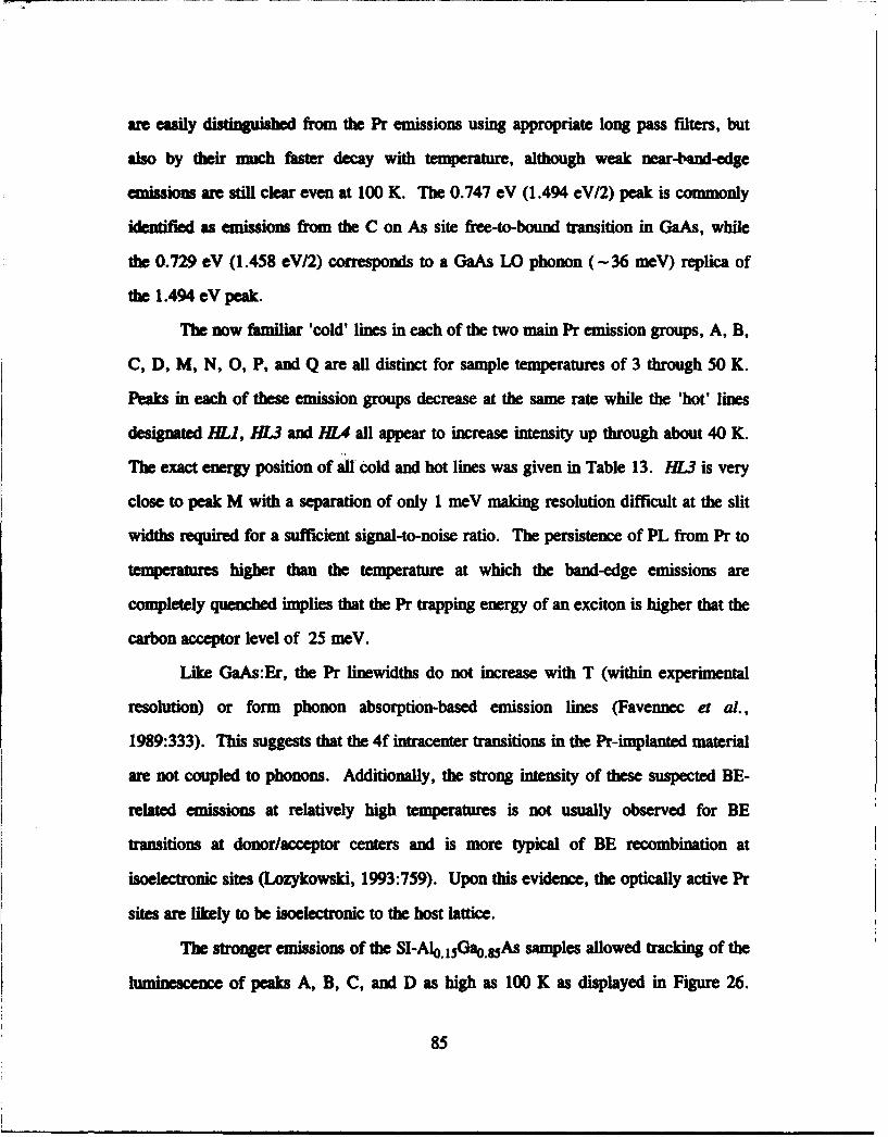
are easily distinguished from the Pr emissions using appropriate long pass filters, but
also by their much faster decay with temperature, although weak near-band-edge
emissions are still clear even at 100 K. The 0.747 eV (1.494 eV/2) peak is commonly
identified as emissions from the C on As site free-to-bound transition in GaAs, while
the 0.729 eV (1.458 eVl2) corresponds to a GaAs LO phonon (-36 meV) replica of
the 1.494 eV peak.
The now familiar 'cold' lines in each of the two main Pr emission groups, A, B,
C, D, M, N, O, P, and Q are all distinct for sample temperatures of 3 through 50 K.
Peaks in each of these emission groups decrease at the same rate while the 'hot' lines
designated/I, 1,03 and BlU all appear to increase intensity up through about 40 K.
The exact energy position of all cold and hot lines was given in Table 13. HL3 is very
close to peak M with a separation of only 1 meV making resolution difficult at the slit
widths required for a sufficient signal-to-noise ratio. The persistence of PL from Pr to
temperatires higher than the temperature at which the band-edge emissions are
completely quenched implies that the Pr trapping energy of an exciton is higher that the
carbon acceptor level of 25 meV.
Like GaAs:Er, the Pr linewidths do not increase with T (within experimental
resolution) or form phonon absorption-based emission lines (Favennec et al.,
1989:333). This suggests that the 4f intracenter transitions in the Pr-implanted material
are not coupled to phonons. Additionally, the strong intensity of these suspected BE-
related emissions at relatively high temperatures is not usually observed for BE
transitions at donor/acceptor centers and is more typical of BE recombination at
isoelectronic sites (Lozykowski, 1993:759). Upon this evidence, the optically active Pr
sites are likely to be isoelectronic to the host lattice.
The stronger emissions of the SI-A0.,a.gsAs samples allowed tracking of the
luminescence of peaks A, B, C, and D as high as 100 K as displayed in Figure 26.
85
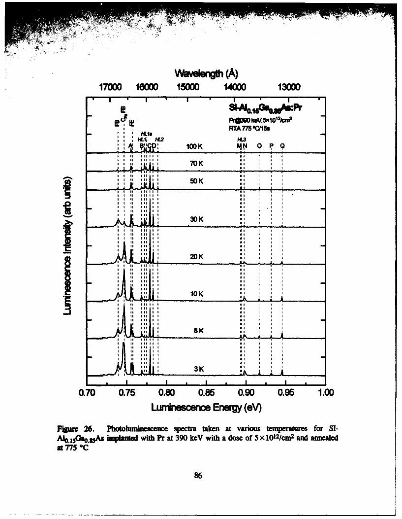
17000 16000 15000 14000 13000N " I * I "
I• •, Pi O koV'SalO'i 2km
RlrA 77 @C31•I I I
ii L4f, M12 11.100_ lK M4I_ 9_F9
I I II III II I NI I I II I II 11II II I II I Ii
,IJ ILJ E NI I I II I If o I7
to-- - I*- i~
I I II II I N I I I I
IIII 1 I51 501 NI I •
II It I I II III I II I NI I IiI I II 1 11 NI# I I I
I I I III I INI I I I
StII I NI
I II I I I 30 N
NIIIIIIII
I II I II IINSI II I II IINI I
SK
fi t II
II III I I I I I I:I III ___________ MI iII III I InI I I I
III III I I N I I III 11 1 NIII I
I NII •
I I __ -____ ____ __ ,____ --
II III II NI I #
II I II IIN I I III III II II I I
I I NIII
IIII I II II NI I I I
II llINIIIII
II I11II I NI I I IIII I II II NI I
II I II I NI
'" ~3K"
III I I NI. I I I
0.70 0.75 0.80 0.85 0.90 0.95 1.00
Lumirlescero Energ (eV)
Fillm 26. Photolmninescence spectra taken at various temperatures for SI-Ak,^5 i01(.implme with For at 390 keV with a dose of 5 x 10¹²/cm2 anld annel~eda 775 °C
II ~1i ______86

The weak peaks M, N, 0, P, and Q were extinguishe almost entirely above 30 K.
More hot fines are evident than in the GaAs:Pr case. hL1i peaks in intensity around 30
to 50 K, while the weaker HLIa and hL2 grow up through about 70 K. HL3 is weakly
seen. 1he second order emission of the CA2 FB 1.494 eV transition from the GaAs cap
layer is again seen at 0.747 eV with no phonon replica, but the other near-edge PL
differs from that of the GaAs case. The 0.739 eV peak (second order of 1.478 eV) is
an undetermined FB or DAP emission, but the 0.758 peak (located next to peak A)
p closely to the second order of the low temperature FE transition of GaAs
at 1.515 eV.
Temperature dependant PL of SI-AIo.3oGao.7oAs:Pr shown in Figure 27
essentially mirrors that of SI-Alo. 5Gao.85As:Pr with much weaker intensity across the
spectrum and with band-edge emissions similar to that of GaAs:Pr. This data is shown
to emphasize the consistency of the Pr hot and cold lines in these Al-bearing hosts. In
this host only peak C has sufficient intensity over the temperature range to allow
meaningful quantitative analysis of the activation energy.
Theoretically, the identification of hot lines should allow assignment of excited
energy states to the upper levels in the transitions. The difficulty in this instance is that
very few hot lines were seen. This allows multiple different energy level assignments
for each hot line making unique upper energy level assignments difficult. For example,
ALI may be associated with excited upper level transitions of peaks A or B. Similarly,
all hot lines in an emission group could correspond to excited upper level transitions
from any lower energy transition in that group. What is needed, but not present, is a
complete set of hot lines with energy spacing identical to those of the cold lines, but
offset by the difference in energy between the lower and upper excited transition states.
87
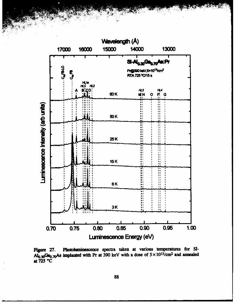
1700 1600 1I00 1400 1300
PwSO h*V,5xlol 3krn2
RTA 725 6Cfl5
SI I pill I
50 ol II I
25 K
fit I II
1I IKI
lot I
6I IKI
3I IKI
0.7 0.75 I8 0.8 0 I 0.9 1.0
Lu* esec Ze K(eV)
Iig 27 IItbiiesec spcr take atvrosmI aue o
A*.0*O7~ imlne ihP5t39 ihads f5 X A03C2adanae
at 725 IIO I I
I 1111 II I88
The integrated luminescence intensities of peak C, Q, and/! H obtained from
SI-Alo.ijGs.&As:Pr are plotted in Figure 28, The behavior of the peak C (0.779 eV
line) and its accompanying emission group show a very interesting behavior of
incresMing intensity over the temperature range from 3 to about 15 K. However, this
increase in intensity does not occur in other emission groups in SI-Al. 15TGa0.gAs:Pr.
Emissions described by the quenching model previously discussed should show only a
continuing decrease in intensity with increasing sample temperature as with the peak Q
in Figure 28 or should increase from essentially zero following a Boltzmann
temperature distribution intensity like the 0.773 eV hot line MLJ. However, peak C
shows a strong intensity even at the lowest temperature, which is inconsistent with hot
line behavior, and an increasing intensity with temperature over a limited range, which
is inconsistent with normal temperature quenching associated with cold lines. A
similar increase in peak intensity with temperature is seen from Alo.45 Gao.4 5As:Er
emissions in figures from a paper by Benyattou et al., but the authors make no mention
of this behavior (Figures 2(a) and (b) in Benyatou etal., 1992:351). The explanation
of the temperature behavior of this peak is not well understood at present.
The strongest cold lines, peaks C and Q, were fitted to Eq (18) to determine
activation energies intrinsic to the excitation mechanism. Since each emission line of
the group varied intensity closely together, the peaks C and Q were chosen as
representative. Single activation energy equation fits were used when an excellent fit
was obtained, otherwise double activation energies were applied. Figure 29 shows the
fit to peak Q in SI-Alo.j5Gao%.As:Pr for parameters corresponding to 2 activation
energies of E1=1.4±0.5 meV and E2=6.0±1.6 meV and for the single activation
energy of E1=9.6±2.0 meV for peak C. Figure 30 shows the fit to peak C in SI-
GaAs:Pr for parameters corresponding to activation energies of E1 = 1.2 ±0.6 meV and
E2=22.5±9.0 meV, and to peak Q using E,=2.2±0.4 meV and E2=28.9±2.9 meV.
89
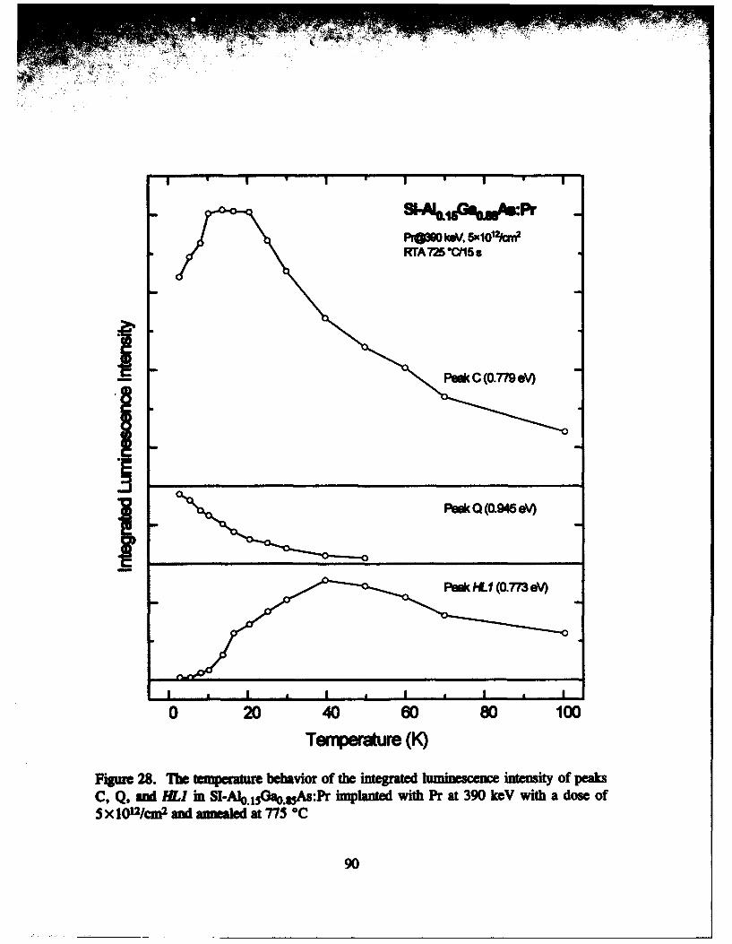
l. •Peak ClO.779 6\0I * I, I , I , I ,
0 20 40 6O 8 1000
Taqx~re (K)
F•m 28. The teprtr behavior of the mtgae himscw intensity of peaksC, Q, ug B.,I in SI-Alo.lSGo.LAs:Pr implanted with Pr at 390 I•-V with a dose of5 x l012/cmA and annealed at 7'75 °C
90
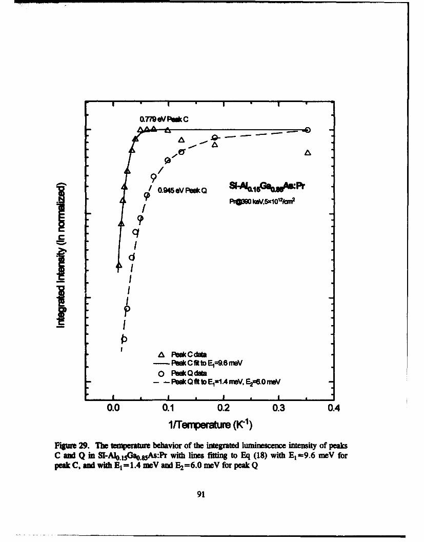
0.779 OV l•k C
Pw OVe kov, Q•o•r
'A FM C dAa
'095e PsCdMto EI9.6 ffMsV
0 Peak 0data=.- - PeOQf5to mEVF.•I.OmfV
0.0 0.1 0.2 0.3 0.4
1/TeMpeatue (K-I)
Fipn 29. 11m teprtr behavior of the integrated luminescence intensity of peaksC and Q in SI-Alo.{o.s•As:Pr with lies ftting to EV (18) with E =9.6 meV forpeak C, and with EE=1.4 meV and E2=6.0 meV for peak Q
91
I I a
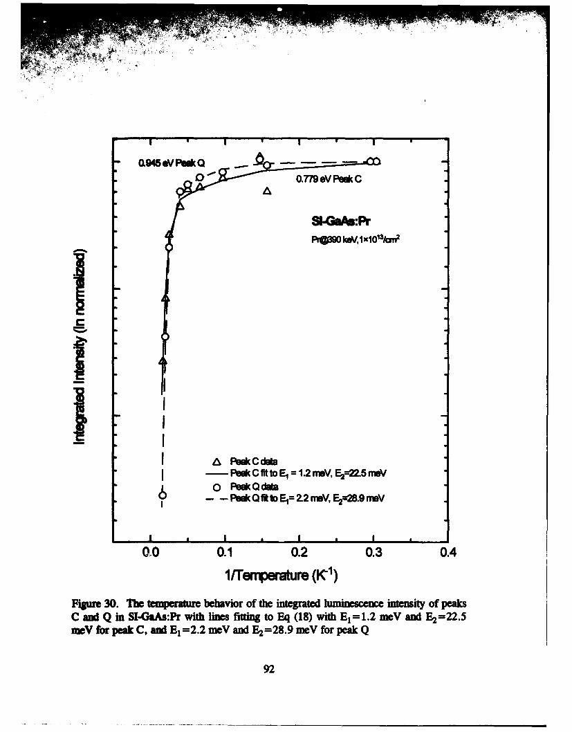
Q94 v Pei a r
Pr[O ka~iiO1 /ai
RO II11 M
- Pedc Oitto Ej=2.2rsV, E2=2a9 msV
0.0 0.1 0.2 0.3 0.4I/TermpeAtur (K-1)
Figure 30. The temperature behavior of the integrated luminescence intensity of peaksC anl Q in SI-GaMs:Pr with lines fitting to Eq (18) with E,=1.2 meV and E2=22.5ineY for peak C, and E, =2.2 meV andl E2=28.9 meV for Peak Q
92

Note that both peaks have the same activation energy pairs within the fining
parameter's standard errors. In SI-AlO.30Gao.70As:Pr, only peak C was strong enough
to conduct a temperature dependence study. This peak gives weak corroboration to the
behavior of peak C in SI-Alo.j 5Gao.85As:Pr, and the effect is small enough that a
satisfactory fit to the simple activation energy Eq (18) could be obtained. Figure 31
shows the fit to peak C in SI-Alo.3OGao.7OAs:Pr for parameters corresponding to Eq
(18)'s activation energy E1=5.6±0.8 meV.
Figures 29 through 31 conform to the typical plot format for PL temperature
dependence. They are displayed using semi-natural logarithm intensity versus inverse
temperature to aid in the quick visual confirmation of the semi-logarithmic linear
behavior of the intensity at higher temperatures. This results from the increasing
dominance of the inverse exponential terms in Eq (18) as T grows. Data from a
sufficiently wide temperature range will include several points in this linear high
t a regime to unambiguously define the activation energy.
Table 14 summarizes the activation energies derived from Eq (18) and the
temperature-dependent PL data for both of the representative peaks. The fits were
determined using TableCurve (Jandel Scientific Inc) and verified using Origin
(MicroCal Inc) or Mathcad (MathSoft Inc). The reported uncertainties correspond to
the standard error reported by TableCurve, where, for a large sample set, about 68%
of the data would fall within these values. The activation energy reported for Peak C
for SI-Alo. Ga .s5As is that of the best fit using E1 in Eq (18). The activation energies
for each host are within fitting uncertainties of each other so no conclusive evidence for
different luminescent centers or excitation paths for the different emissions groups is
seen. Lacking other evidence, these emissions must be considered to emanate from a
common Pr luminescent center through a common excitation process.
93

9 -
0.779 eV Pek C 0 0
PeM keV,5x10 131cm2
0 Peak CdiatPdC fit to Eý:5.6m=V
I , I I * I
0.0 0.1 0.2 0.3 0.4
lTref nrature (K-)
Figure 31. The temperature behavior of the integrated luminescence intensity of peakC in SI-Alo.3oGa.o.As:Pr with lines fitting to Eq (18) with E, =5.6 meV
94
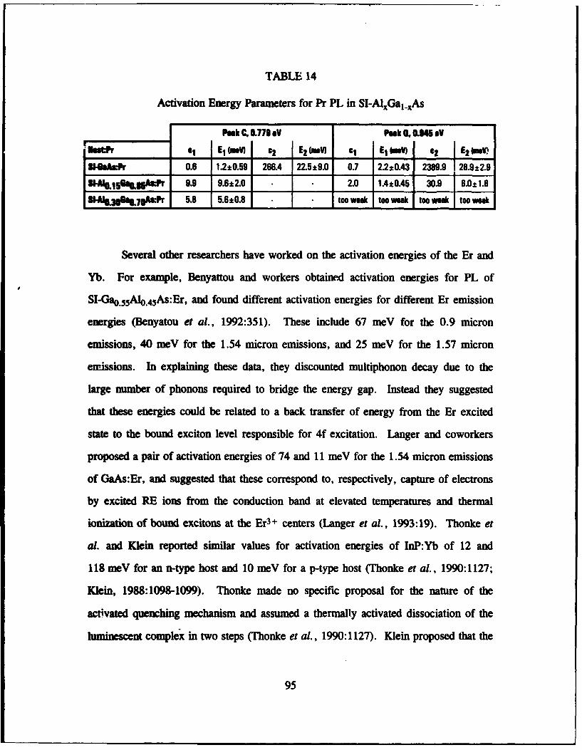
TABLE 14
Activation Energy Parameters for Pr PL in SI-AlxGal-xAs
Pek C. 0L771 eV Peak I.L &46 @V
'Ust1 El E(MV) 02 E2 (Novi C1 El I=V) c2 EZ (anIP
UHsAsr 0.6 12.20.59 266.4 22.5,9.0 0.7 2.2±0.43 2389.9 28.9±2.9
tEAIl 15 uL1 Amdr 9.9 9.6±2.0 2.0 1.4±0.45 30.9 6.0±1.6
I.Al.nf 7 jftfAatr 5.6 5.0.8 too weak too weak too weak too weak
Several other researchers have worked on the activation energies of the Er and
Yb. For example, Benyattou and workers obtained activation energies for PL of
SI-Gao.55A 0o.45As:Er, and found different activation energies for different Er emission
energies (Benyatou et al., 1992:351). These include 67 meV for the 0.9 micron
emissions, 40 meV for the 1.54 micron emissions, and 25 meV for the 1.57 micron
emissions. In explaining these data, they discounted multiphonon decay due to the
large number of phonons required to bridge the energy gap. Instead they suggested
that these energies could be related to a back transfer of energy from the Er excited
state to the bound exciton level responsible for 4f excitation. Langer and coworkers
proposed a pair of activation energies of 74 and 11 meV for the 1.54 micron emissions
of GaAs:Er, and suggested that these correspond to, respectively, capture of electrons
by excited RE ions from the conduction band at elevated temperatures and thermal
ionization of bound excitons at the Er3+ centers (Langer et al., 1993:19). Thonke et
al. and Klein reported similar values for activation energies of InP:Yb of 12 and
118 meV for an n-type host and 10 meV for a p-type host (Thonke et al., 1990:1127;
Klein, 1988:1098-1099). Thonke made no specific proposal for the nature of the
activated quenching mechanism and assumed a thermally activated dissociation of the
huninescent complex in two steps (Thonke et al., 1990:1127). Klein proposed that the
95

large activation energy was comparable to the binding energy of a hole to a neutral Yb
acceptor and possible involvement of a population of non-equilibrium carriers which
recombine with carriers trapped on defect centers (Klein, 1988:1098-1099).
With these past analyses in mind, the Pr activation energies may now be
explained. The higher activation energies for each host (>4 meV) probably
correspond to the dissociation of excitons bound to the Pr ions. The lower activation
energies (<4 meV) are attributed to the effect of the hot lines of each group which
depopulate the bottom most upper level states of the cold line transitions such as those
monitored for these activation energy calculations. This implies that, for GaAs:Pr, the
next higher state of the 3F3 excited energy level is - 1.2 meV above that from which
the 3F3-+-3H4 emissions emanate, while the next higher state of the 1G4 level is elevated
by -2.2 meV. A similarly small activation energy for the 0.945 eV peak from
Alo. 15Gao.8As:Pr implies that the next upper state of the 104 level is elevated by
1.4 meV which is consistent with the value 2.2±0.5 meV observed for GaAs. The
previously discussed pronounced increase in Pr peak C up through 40 K no doubt
overwhelmed any small hot effect on this peak, so no hot line-associated activation
energy was found for this peak. These small implied crystal field splittings are similar
to the splittings of PL lines as low as 4 meV and are near to the smallest hot line states
of about 0.9 meV (peak /L3 to M), 2.7 meV (peak HL4 to P) and 3.5 meV (peak IL1
to B) (for GaAs:Pr in Table 13). This hot line quenching effect will probably be much
weaker than that of trapped carrier dissociation at Pr sItes, which is confirmed by the
smaller c coefficients for the smaller activation energies associated with the hot lines.
Selectiye Excitation of Pr Luminescence
The selective excitation experimental results gave direct insight into the
excitation mechanism of Pr in AlxGa..xAs hosts. After calibration of the tunable
96

Ti:Sapphire laser wavelength versus position, a computer program was coded to
automatically control the output wavelength of the laser, collected data from the
detector, calibrated and stored the data. The uncertainty of laser excitation energy
measurements reported in this section stems from the standard error of the equation
used to fit the laser calibration and is ±3 meV. The laser was tuned from 7070 A
(1.75 ev) through 8600 A (1.44 ev). The low temperature direct bandgap of
AlxGaxMAs was calculated from experimentally determined parameters reported
recently. The direct bandgap as a function of the Al mole fraction x, E8 (x), is defined
by (El Allai et al., 1993:4403)
E.(x) = EGa, +ax+bx2, (21)
where Eg,& is the GaAs bandgap at T=0 K given as 1.519 eV, and a andb are
fitting parameters which were determined to be af= 1.447 eV and bf=f-0.15 eV for T=0
K. Since this empirical equation is valid only for direct gap material, the range for x is
0.0 to 0.4. This gives bandgaps of 1.52 eV for GaAs, 1.73 eV for Alo.15Gao.S5As, and
1.94 eV for Alo.3oGa.0 7OAs (2.07 eV for Alo.5oGao.5oAs as noted previously). Thus the
selective excitation spanned from above to below bandgap energies in both low
temperature GaAs and Al.153Gao.As. For the other hosts the excitation energy ranged
below gap from about 186 to 493 meV in Alo.3oGao.7oAs and about 316 to 623 meV in
Al.5oGao.0As. For comparative uses, the values of the free excitons in these hosts is
determined again from Eq (20). The strongest emission peak in each group was used
as the monitor (0.779 eV peak C and 0.945 eV peak Q) and the intensity data for these
peaks were collected at approximately 5 A intervals of the excitation laser wavelength.
Tests were run on optimally Pr-implanted and annealed SI-GaAs:Pr,
SI-AIo.15Gao.S5As:Pr, SI-Alo.3oGao.7oAs:Pr, and SI-Alo.5oGao.5oAs:Pr, however tests of
SI-AJo.3oGao.7oAs:Pr and SI-Alo.5oGao.5oAs:Pr revealed no Pr-related luminescence
97

Is wý owu the emsire excitation energy range. This is due to the excitation
emrgime of the laser which were well below bandgap for both.
Figure 32 shows the SEL luminescence behavior of peak C in the
SI-AlOa 0 .sG..,As:Pr host which was found to be identical to that of peak Q. The
itnsity of both peaks increase slightly as the laser energy moves below the bandgap
of the host and starts to decrease sharply at a laser energy of about 11 meV below Eg.
The luminescence was further monitored to over 280 meV below the bandgap energy,
but no Pr luminescence was observed over this range. This common behavior of each
emission group is evidence for a shared excitation mechanism step related to the free
carriers, excitons, and near band-edge emissions. The PL intensity drop is very
distinct, and occurs at 1.720±0.003 eV which is about 11 meV below the band-edge
which agrees well with the activation energy of 6.0 to 9.6 meV for these peaks (Table
14). The half-mximm point of the intensity drop off is shown to be 21 meV from the
band-edge energy. Since energies near the free exciton energy are required for
luminescence of Pr in these hosts, free carriers, excitons, x free-to-bound
transitions must be considered essential for the Pr excitation process.
Figure 33 shows similar behavior from the SI-GaAs:Pr sample. The intensity
drop of both lines is abrupt as the excitation energy dips below the exciton energy level
of GaAs at 1.515 eV. The intensity drop occurs over a narrow range with the half-
maximum point for this host being only 5 meV below the FE level (half that of SI-
AI0 .IGao.ssAs case). Peak Q also has a clear, below bandgap energy maximum
centered at 1.496 eV (24 meV below the bandgap energy) which appears to be about
20 zneV wide. This peak may result from pumping directly to the BE energy level at
the Pr ion site since 24 meV is close to the activation energies assigned to BE
dissociation for SI-GaAs:Pr (22.5 and 28.9 meV). Thonke et at. reported similar
photolumi escence excitation behavior of YW+ in InP with a very steep drop of Yb-
98
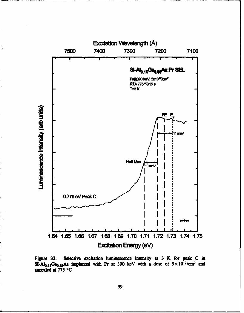
EctWtOn Vavekenth (A)7500 7400 7300 7200 7100
Sk%.Gl•=ofpr S.
RTA7750015sT=3 K
FEE
O.M~evftC
'!
1.64 1.65 1.6 1.67 1.68 1.69 1.70 1.71 1.72 1.73 1.74 1.75E t t Energy (eV)
Figure 32. Selective excitation huminescence intensity at 3 K for peak C inSI-Ao.1 ,oGa•.s implanted with Pr at 390 keV with a dose of 5xl01 21cm2 andamnled at 775 °C
99
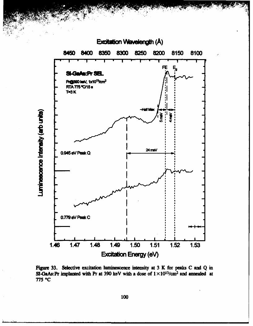
Excliton V~bvaerengt (A)8450 8400 8350 8300 8250 820 8150 8100
FE81afPr SELPow0 W, ixio%ifRTA7TB15"5sTW3 Ka
4wmI
I24"w4I r Qve~
O rm .. w Pa a
1.46~~ ~ ~ 1.714 .915015 .215
Excta iaEIW(V
Fig= 3. Secdve xciteon inmity at o pab dQiSI-GM:PrimpntedwithPr t 39 kcVwM dos ofI X I03C2aWa~Wa
775 OC~
100
related emsioms below excitation at the FE energy and a small maximum at about
33 meV below the InP bandgap energy (Thonke et aa., 1990; 1125). These workers
concluded that this CB-33 meV peak could correspond to a process in which electrons
tapp at the Yb ion (treated as a pseudxdonor) are excited either to EMT states (still
bound to the localized hole) or directly to the CB (Thonke et al., 1990; 1129).
Pomrenke et a!. reported SEL results on GaAs:Pr, which were limited to fairly
coarse excitation energy steps due to the use of a tunable dye laser (Pomrenke et a!.,
1990:333-334). They reported that the luminescence of a 1320 nm line (0.939 eV)
drops in intensity near the free exciton energy, however the coarseness of the excitation
energy steps also jumped over the below gap maximum at 1.497 eV. They did not
report SEL for the 1592 nm line (0.779 eV) for any excitation energies less than
1.51 eV, which were seen in this study down to 1.47 eV (Figure 33). However, for an
excitation energy of 1.386 eV, they reported a spectra with weak, sharp Pr lines quite
dissimilar to those found for above gap excitation. These different Pr lines are
attribmted to multiple Pr centers, but the possibility of some sharp lines emanating from
residual transition elements and other impurities was not excluded.
The lack of Pr luminescence for excitation energies less than about 25-30 meV
below the host badMgap is in strilkn contrast to the behavior of Er in GaAs. Colon et
al. reported strong Er PL from the 1.538 micron line for laser excitation energies as
low as 960 um (1.29 eV or 228 meV below GaAs bandgap) along with Er-related deep
hole traps (Colon et a!., 1992b:673). These researchers proposed that the below-gap
excitation ionized electrons from these Er-related hole traps into the CB and the
remaining bound hole recombines with an electron, thus pumping the Er luminecence.
In this present study, the lack of any below-gap excitation-based luminescence ranging
from 186 to 623 meV below the gap of hosts examined gives evidence to infer then that
no such Pr-related deep hole traps exist in the hosts tested here.
101
The cmmon carcteristIs of ewah of these SEL data sets is the sfficiency of
Su~ gat or slightly below the FE energy of the host for inducing Pr in.
It is appment that Pr luminescence in these hosts can only be puped with energies
capable of creating free carriers or free excitons, with the singular possibility of direct
pumping to the BE energy levels at the Pr ion.
Ptmmlnm1.21Du&W Pr 2an Er
In order to evaluate the effect of introducing 2 different RE elements into a
semion , both Pr and Er were implanted into AlxGal.xAs hosts. It was hoped
that the energetic interaction between the two ions might serve to facilitate stronger
near IR emissions than either would produce separately. There are 2 competing
mechanisms which affect luminescence of REs in the same host. First, separately, both
REs compete for available free excitons for their energy source. Second, the ions may
pair up, forming heterogeneous rare earth complexes. These complexes may facilitate
the transfer of BE recombination energy by providing energy level combinations which
are well matched to BE energy.
For this study, Er was implanted with an energy of 1 MeV at doses of 1 X 10¹³
and 5 x 10¹³/cm2 . Host semiconductors included SI-GaAs, and SI-AIxGal-xAs with
x=0.15, 0.30, and 0.50. Portions of these hosts were implanted with Er only, with
both Er and Pr, and with Pr alone. All samples implanted with Pr were at 390 keV
with a dose of 1 x 10¹³/cm2. The implant depth of Er peak concentrations into these
hosts spans a range of 1833 A in GaAs to 2048 A in Ao.oGao.0 As as shown in Table
15. Although these implant depths are roughly twice their Pr counterparts (Table 8),
this is actually advantageous when combined with the dosages used. For the low Er
dose, the Er and Pr implant profiles are essentially separate as shown in Figure 34.
The corresponding results may be viewed as nearly independent luminescence from
102
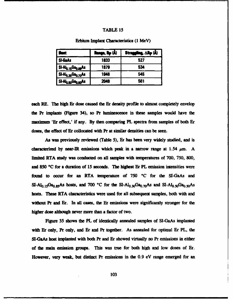
TABLE 15
Erbium Implant Characteristics (1 MeV)
Nat Mq W Rp() Sa* ,R ASMAS 1833 527
SI-AI&3gaAk 1870 534
SI-AIoG.ao 7ofA 1948 545
%A6AI.WbA 2048 561
each RE. The high Er dose caused the Er density profile to almost completely envelop
the Pr implants (Figure 34), so Pr l in these samples would have the
maximum 'Er effect,' if any. By then comparing PL spectra from samples of both Er
doses, the effect of Er collocated with Pr at similar densities can be seen.
As was previously reviewed (Table 5), Er has been very widely studied, and is
har atred by near-IR emissions which peak in a narrow range at 1.54 gm. A
limited RTA study was conmlud on all samples with temperatre of 700, 750, 800,
and 850 °C for a duration of 15 seconds. The highest Er PL emission intensities were
found to occur for an RTA temperature of 750 °C for the SI-GaAs and
SI-AMo.01 Gao.sAs hosts, and 700 -C for the SI-Alo.3oGa.O.7 As and SI-Alo.joGaO.5oAs
hosts. These RTA characteristics were used for all subsequent samples, both with and
without Pr and Er. In all cases, the Er emissions were significantly stronger for the
higher dose although never more than a fctor of two.
Figure 35 shows the PL of identically annealed samples of SI-GaAs implanted
with Er only, Pr only, and Er and Pr together. As annealed for optimal Er PL, the
SI-GaAs host implanted with both Pr and Er showed virtually no Pr emissions in either
of the main emission groups. This was true for both high and low doses of Er.
However, very weak, but distinct Pr emissions in the 0.9 eV range emerged for an
103

IN. 'a 0 0PII-ak
484
is
420
1.5 Pahow kb
8 1.0 X13mO.5
0.0
0 1000 M00 3000 4000Depth(A
Figure 34. onertIdn profiles of Er and Pr implanted into Alo IGaojAs as usedinthe dal-doping sady
RTA temperature of 800 *C (higher than the optimal temperatue for Er) as shown in
Figure 36. Dotted guidelines are displayed to distinguish the major emission lines
from each RE. The Er 4113f2-+41Ifl transition emissions are only Slightly decreased by
the presence of Pr, while the Pr emissions are seen to be completely exigihdby
the presence of Er.
The intrinsically stronger Pr emissions from AJO.IG%.SAs aliowed a more
interesting ivsgaonof the emissions from this dual-doped host. The upper traces
in FIgur 37 show typical Er-ouzly lumnescence, which is very similar to that of the SI-
GaAs host, however the PL firom a host containing both of Er and Pr depends on the
couMEratve doses of the implants (Figure 37 lower trace). For equal doses, here
1 x 10131cm2, the Pr emissions are stonger than thos of Er, but with the Er dose
104
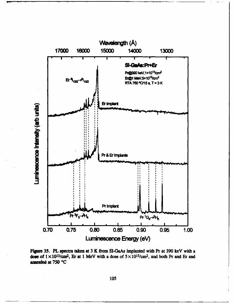
Vavelengt (A)17000 16000 15000 14000 13000
• I " II IF
PrQaeo k1eV, 3xlOut 2
Er1-. MVSxl0o3kb2RTA 750 C015 s, T= 3 K
gg1
Iffu
J ,,VIll II
mmtmW• '•3F3._A14 Pr 1G4--•J q
S I IN I a I a I a , I
0.70 0.75 0.80 0.85 0.90 0.95 1.00
Lurinescence Energy (eV)
Figr 35. PL spectra taken at 3 K from SI-GaAs implanted with Pr at 390 keV with adose of 1 x10 13/cm 2, Er at 1 MeV with a dose of 5 x 10 3/cm2, and both Pr and Er andanneald at 750 °C
105

VWaysength (A)17000 16000 15000 14000 13000
ErGl MAV5x1O' 3Iai9
T=3K
Er~i,,2-,,.2Pr IG4-0'iN
RTA85O'CVl5sL
dos of I I03c2adE tIMVwt oeo 03C2adawda*10

VWveengt (A)17000 16000 15000 14000 13000
Er1310240112 Eral MdVRTA 750OC/15 , T 3 K
B05X1O 1 3/Crr?
E,@1X10131av9
a ar9WkmVlXlOIkn 2
ar a aV
0.70 0.75 0.80 0.85 0.90 0.95 1.00Lurrnecence Energ (eV)
Figur 37. PL spectra taken at 3 K from SI-Ali.,GaAs implanted with Er atI 11eV with a doses of I x1013/cm2 and Sx 1O' 3/cm2 with and without Pr at 390 keYwith a dos of 1 X 10¹³/CM2 ami annealed at 750 OC
107

V -. - At. .• i:
uueued by a factor of five, the Er emissions increase strength at the cost of the Pr
intemsity. This implies that no luminescence enhancement is occurring, and that the
two REs are competing for pumping energy from the lattice. The higher density RE
will capture a greater percentage of the available free carriers and excitons. If any Pr-
Er complexes are forming, they are not significantly affecting the luminescent behavior
compared to the corresponding singly implanted hosts. This effect is demonstrated
again by comparing the three variants in this study as shown in Figure 38. The sample
with pure Pr shows the familiar pair of strong emission groups, while the Er-only
sample shows similarly strong emissions albeit with a higher dose. When these REs
are combined, as shown by the center trace in Figure 38, both RE emissions are
strongly diminished.
Figure 39 displays the PL spectra of SI-Alo.IoGa0.7oAs implanted with Er only,
Pr only, and both Pr and Er. Both RE emissions decreased slightly when they were
dual-implanted, but the effect is not as dramatic as in the earlier two cases. Figure 40
displays the PL spectra of SI-Alo.5oGaoOAs implanted with Er only, Pr only, and both
Pr and Er. This host exhibits different behavior in that the Pr emissions, although
weak, seem slightly enhased by the presence of Er, while the Er emissions are
essentially unchanged. This increase in Pr intensity is also accompanied by a decrease
in the broad-band defect emissions centered near 0.82 eV in the dual implant case.
With both of these apparent effects, it is difficult to assign a specific reason for the
enhancement of the Pr emissions, especially when it is so contrary to the results of Pr
PL from the other three dual-doped cases in this study.
Figure 41 shows graphs of the PL spectra from each of the SI-AlxGal-xAs hosts
implanted with Pr at a dose of 1 X 10¹³/cm 2 and Er at a dose of 1 X 10¹³/cm 2 , while
Figure 42 shows the results of duplicated experiments for an increased Er dose of
5 x 10¹³/cm 2. For this case of equal amounts of Pr and Er in the lattice, neither RE PL
108
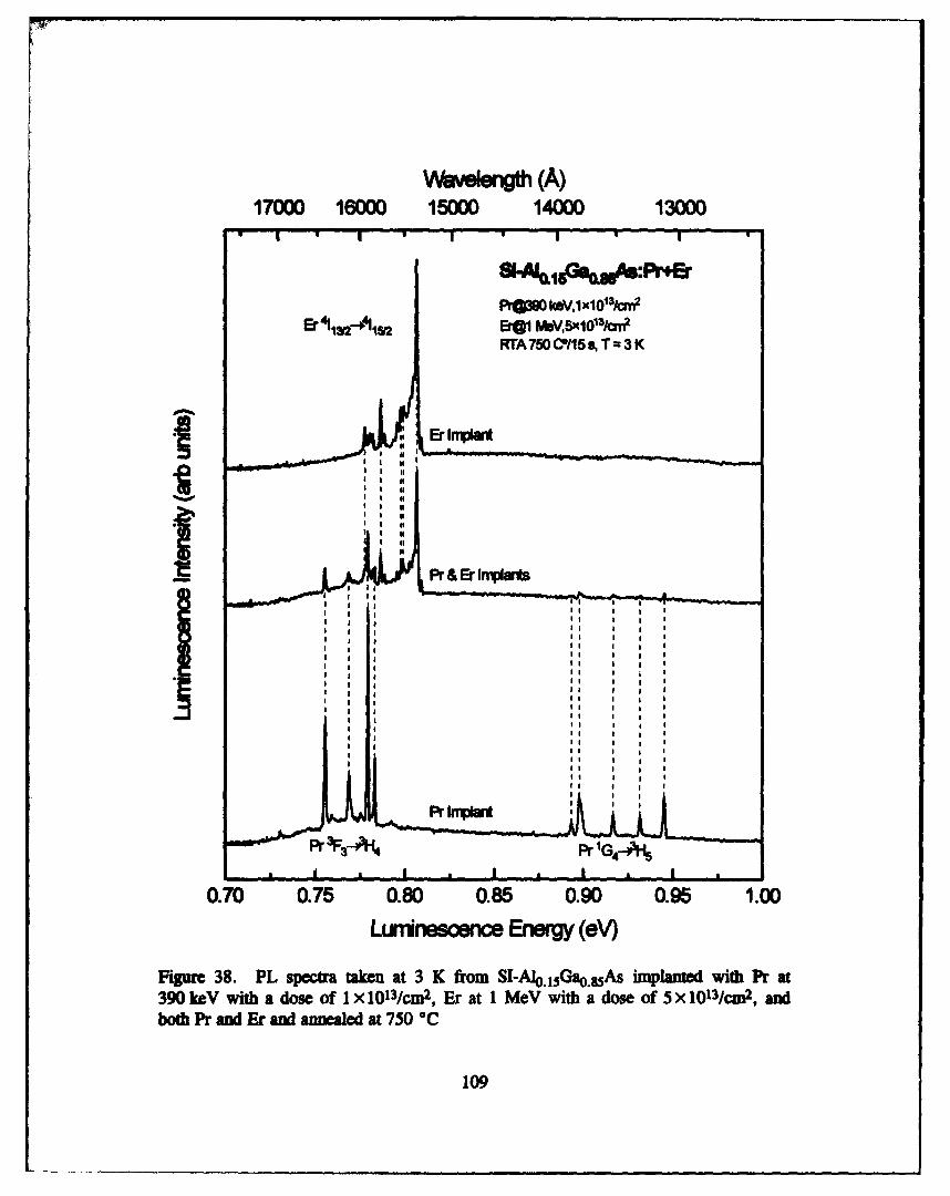
Wavength (A)17000 16000 15000 14000 13000
'! ' I ' " ' ' • ' I .... .
Pr4GOk9V.1x1oI3/A~ft
= 12, RTA75lC'/5osTm3K
VI Pr & Er MVvxOt
0.70 0.75 0.80 0.85 0.90 0.95 1.00
Lunrinescence Energ (eV)
Figur 3 8. PL spectra taken at 3 K from SI-Al0*15Gao.8As implanted with Pr at390 keV with a dose of I x1013/cm2 , Er at 1 MeV with a dose of 5 X10 13/cmn2, andboth Prand Er amtannealed at 750O0C
109
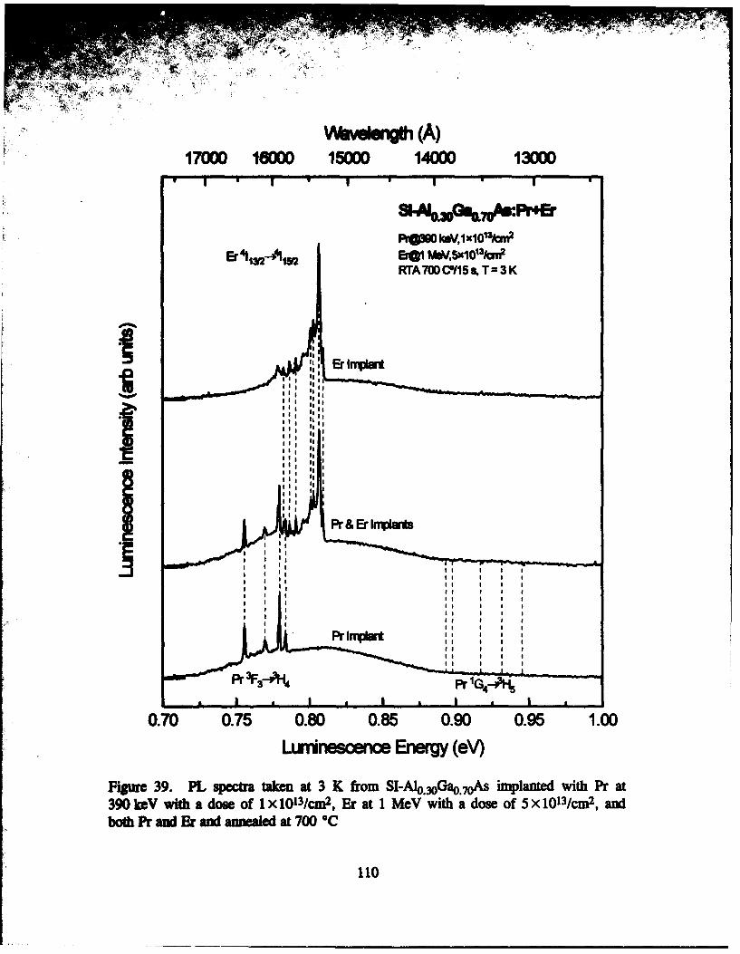
wave kNgPauh (A)17000 1600 15000 14000 13000
Er~l 132-AIP2 O kWVýXIO3 kbn2
Er@ MII5xO'3ut
a I A I m I aI m 1 1
0.70 0.75 0.80 0.85 0.90 0.95 1.00Lunrinescenc Energ (eV)
Figur 39. PL spectr taken at 3 K from SI-A10*~Ga070As implantd with Pr at390 keV with a dos of 1 X10 13/CM2, Er at 1 MeV with a dose of 5 Xl0 131CM 2, andbod Pr and Eran&W ann alea 700 OC
110
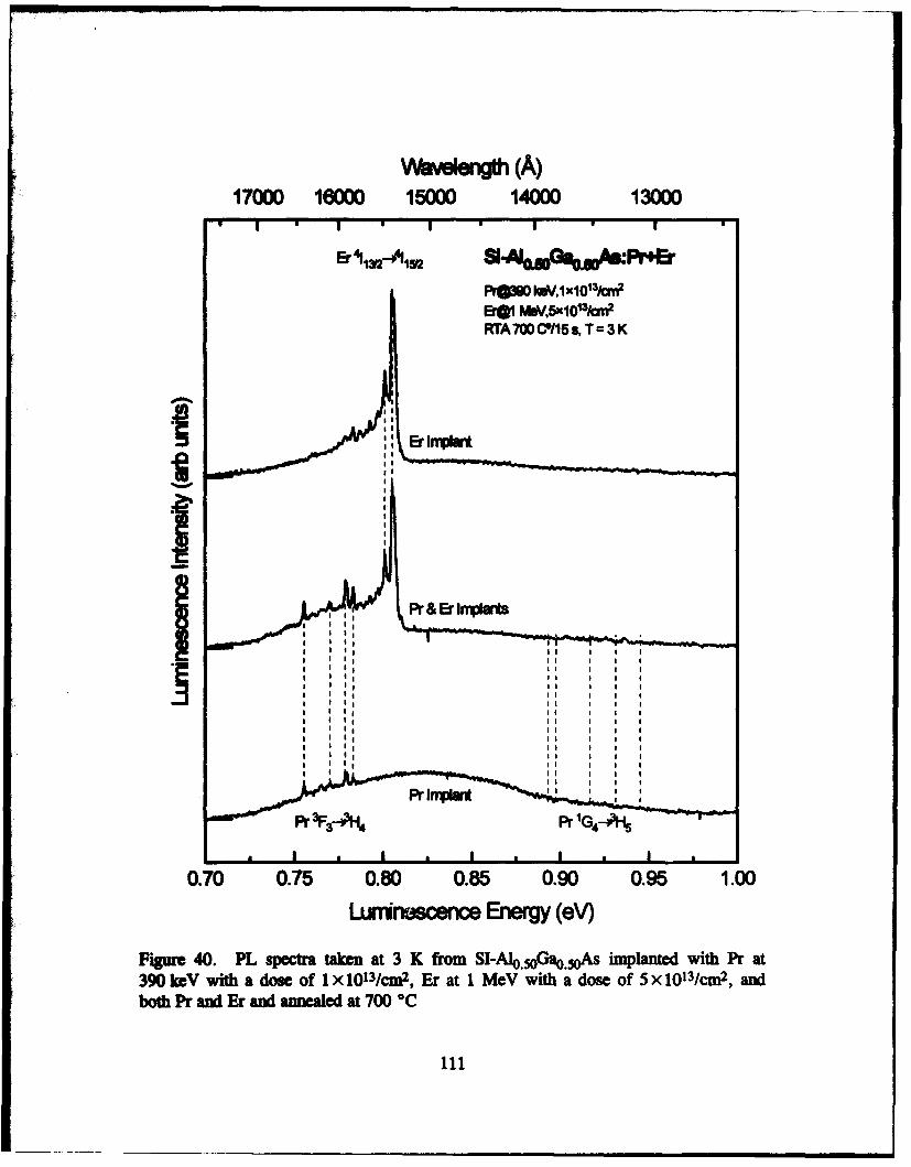
17000 1600 15000 14000 13000
Er 'y,-A. SI-MG%,,fPr4&
Pr9OMMO.1x0 13ftn2
ErSI MWb,5XlO13kn,2
p I * II * I I t
0.70 0.75 0.80 0.85 0.90 0.95 1.00
Luninoscence Eneg (eV)
Figure 40. PL spectra taken at 3 K from SI-AJo.5Ga.SAs implanted with Pr at390 keV With a dose of 1 X10¹³/cm,2, Er at 1 MCV with a dose of 5 X10 131CM 2, andboth Pr andEr and annealed at 700 0C
III
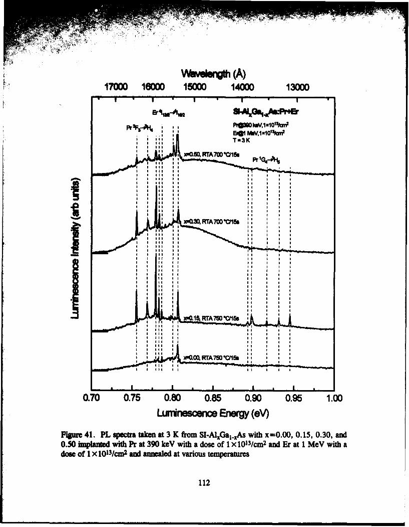
F, 7. 7r
Wv~ieength (A)
a a aQO xORrA700 C/15s
0.70 0.75 0.80 0.85 0.90 0.95 1.00Luninescenc Energ (eV)
Figur 41. PL specta taken at 3 K from SI-AlxGal.,As with x=0.00, 0. 15, 0.30, and0.50 implantd wfth Pr at 390OkeV with adose of I X10 13/cm2 and Er at 1 MeV with ados of 1 X 10¹³/CM2 and anneled at various temperatre
112

17000 16000 15000 14000 13000
U I * I oilI
Si-Al
xo*( ar75 PiTA In5BxO~
a -Ja
doe f X103/M2Md&MaW at VarTA7CCJ
a Sam113
ram ID be damiumt. 11e grsher Er atom depth (dh to highe ini=m eMery)
sAxii m not the Er PL iztcmky with respect to increased abs of the exiting
Er lumunsce, but the laser excitation energy will be reduced at the greater depths.
Thus direct comparison of the intensities is inconclusive. However, for the case of the
high Er dose with a five-fold increase in atoms over Pr, the Er PL is increased at the
expense of the Pr PL (Figures 35, 38, 39 and compare Figures 41 and 42), since there
is a much greater number of Er atoms in the implant region.
The significant decrease in Pr PL in the presence of even the low dose Er
(bottom spectrum in Figure 41), where the Pr and Er are mostly separated in the
lattice, suggests that the apparently shared energy source (free carriers/excitons) is
mobile at least within the 2000 A implant region. If the free carriers/excitons were
created by the laser and immediately absorbed only by local RE atoms, then no
decrease in lui escence from either RE should have been observed.
Although the dual-doping of Er and Pr did not increase the lumincence'
intenity as hoped, important information can be gleaned from this data. Summaizing
the results from this dual Pr and Er implantation study, the PL intensity from each RE
in dual-doped samples was reduced compared to their singly doped counterparts. The
energy positions and relative intensity of the PL emissions are essentially unchanged
within each of the RE emission groups. Thus, no discernible interaction between the 2
different RE ions is occurring and their luminescence processes are essentially
independent, although apparently competing for the same energy source. This is
attributed to a failure of the Er and Pr to couple energetically, either because they are
generally too distant in the lattice or an intrinsic inability of Pr-Er pair complexes to be
excited simultaneously by Auger energy transfer.
114
Adding additiodl elements to the host:Pr compound, such as lighter atoms, is
hoped to enhance the Pr emissions. These extra elements may enhance emissions
1"Iigh formation of complexes with Pr. These complexes may then (1) have a greater
pobsbility of binding an exciton, or (2) make the transfer of exciton recombination
eneri moe likely. The formation of these complexes is especially likely due to the
geasPring effect of REA in general.
Since no codoping studies have ever been reported on Pr, the codope elements
for this effort were chosen based on elements shown to enhance Er PL in Si (Michel et
at., 1991:2675). These include B, C, N, 0, and F, which were implanted at doses of
1x10 14 and 1x10 15 /cm 2 into semiconductor hosts both without and with Pr
im-platation at 390 keV with a dose of 1 x 10¹³/cm 2 . The larger doses for the codope
ele is were chosen to increase the possibility of interaction with the Pr ions. The
host sekused in this study include SI-GaAs and SI-Alo.14Ga 60.8As. In
addition, SI-AI05G0.S5 As:Pr was implanted with oxygen as a consistency check
between host wafers from different growth dates. The implantation energies for each
of the codope elements were carefully chosen to closely align the peak implant densities
of all codope implants with that of the Pr density profile. Since, for practical economic
reasons, only one implant energy had to be selected for each element, the profile of Pr
in Al0 .15Go..As was chosen as the benchmark. Slight differences in the Pr depth
profiles in the other hosts should make no significant difference in the resultant
luminescence. Table 16 shows the implant energy used for each of the codope
elements along with the implant depth information supplied by the PROFILE code.
Comparison to Table 8 shows the difference in depths from Pr to be minor, especially
commared to the projected straggling ranges. Figure 43 shows a representative
comparison of the concentration of Pr and C atoms for the implantation parameters
115
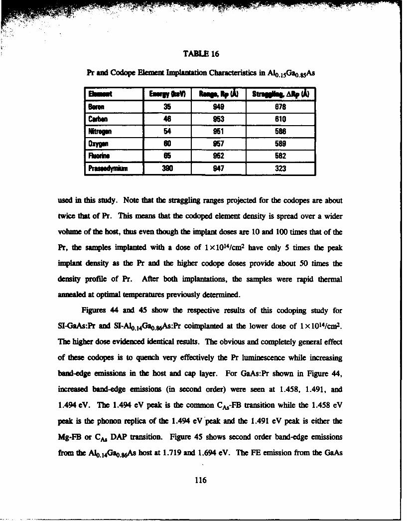
TABLE 16
Pr and Codope Element ImlnainCharacteristics in AI15G%,LAs
_____ _ EMrg INV) NowiI NP(k SUWi-- -W(0ron 35 949 678
Cuben 46 953 610NtrogM 54 951 586
Oxygen 60 957 589Fkwkn 65 952 582
Prfmdymium 390 947 323
used in this study. Note that the straggling ranges projected for the codopes are about
twice that of Pr. This means that the codoped element density is spread over a wider
volume of the host, thus even though the implant doses are 10 and 100 times that of the
Pr, the samples implanted with a dose of 1 X 10¹⁴/cm2 have only 5 times the peak
implant density as the Pr and the higher codope doses provide about 50 times the
density profile of Pr. After both implantations, the samples were rapid thermal
annealed at optimal t tures previously determined.
Figures 44 and 45 show the respective results of this codoping study for
SI-GaAs:Pr and SI-Alo.14010.86As:Pr coimplanted at the lower dose of 1 X 10¹⁴/cm2.
The higher dose evidenced identical results. The obvious and completely general effect
of these codopes is to quench very effectively the Pr luminescence while increasing
band-edge emissions in the host and cap layer. For GaAs:Pr shown in Figure 44,
increased band-edge emissions (in second order) were seen at 1.458, 1.491, and
1.494 eV. The 1.494 eV peak is the common CAs-FB transition while the 1.458 eV
peak is the phonon replica of the 1.494 eV peak and the 1.491 eV peak is either the
Mg-FB or CA3 DAP transition. Figure 45 shows second order band-edge emissions
from the Al0.14Ga0. 6As host at 1.719 and 1.694 eV. The FE emission from the GaAs
116

-anI I-I A
{6.4
I * • I * a * I
0 500 1{10 1500 2000 2500 3000
F]gur 43. Cosx:ntrtlo profiles of C: a.., Pr •imlntd into Al0 .,G•, s. a use ino
cap layer is als semi at 1.513 eV along with the C,,.-FB emisio at 1.494 eV. The
(3a emI~iom dll• sliglwy due to the difrn growth mehd of the two sample
with an LEC-grown Gau~s susrt used in Figure 44 awl MOCVD-grown GaAs in
Fiue45. The Al0o 5as g5Ao. :P sample is imlie with oxygen behaved exactly as
theSI-AlIo~ 4G%j.A:Pr+O sample with complete quenching of the Pr PL for both
I g al low oxygen doses.
The effect of the codope elmet is likely to be either competition for the
available free carinlexcltons'or de-activation of the luminmesnc Pr ions through
foiunatlon of nm-Aiminesen Pr'-codope compglexes. Agin the reut of Pr and 0
coaigshow the strn cotrs with Er anl 0 codoping for both GaAs and A~~
wlchshowed strong enacnn of the Br-rlteld emissions (Colon et a!.,
1993Jb:216; Colon at aL., 1993a: 169).
117
n0- .. ....... .......... ... ... ...

RAN ~
VOW0 IS= 1500 14000 13000
v W
It I~etP
I Ik~llo n
I W@~ j1 ia
* aO5o =3
N
FG0 I9
fekoI Ik9
I Iko
BI3 kI
3F3^
Ir Ir
II 0.I08 .5 09 .510
Irrmm InW(V
Figm~~~~~~~~ 44 Isetatbna fS-as mlne ihP t30kVwt
4m~~~~~~~ ~ ~ ~ of1112adcf dwt ,C ,0 rFa nrisiniaewthads
of I04ck n oe t80O
118
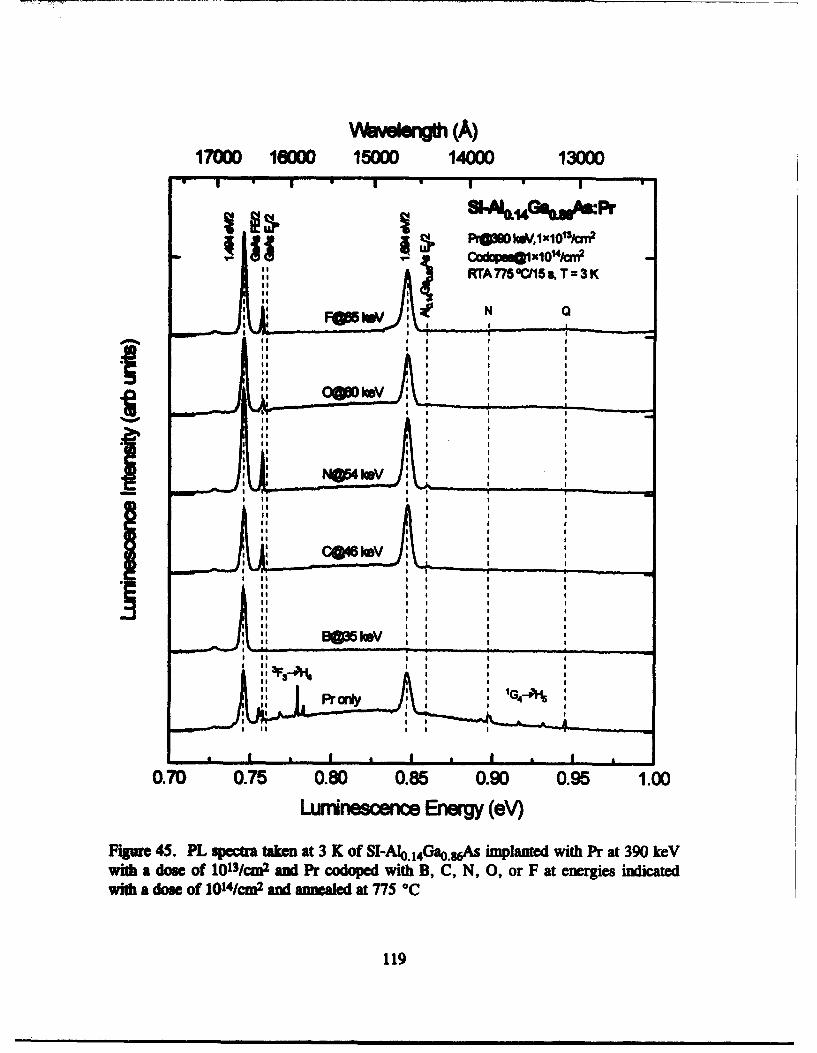
W~w~ength (A)17000 16000 15000 14000 13000
II07 07 00 8 090.1.
u$ " uinsene nrg (VFiur .eiwwoRTA7"Te sdaN
119
||9 k
A| i|l,
||ke
NWI9
C oem
||ko
0.70 0.75 0.8o 0.85 0.90 0.95 1.00Lwuirwoenm Energ (eV)
Figure 45. PL spectra talen. at 3 K of SI-A.1o.14Gao.s6As implanted with Pr at 390 keYwith a dose of 1013/cm2 and Pr codoped with B, C, N, 0, or F at energies indicatedwith a dose of 1014/cm2 and annealed at 775 °C
119
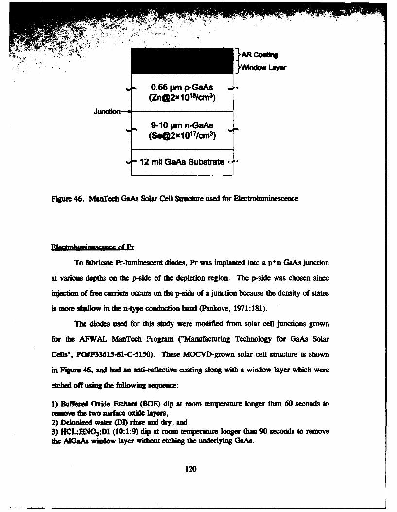
(Zn2x I0'8/cm3)Junctin-
9-10 pm n-GaAs(,S xl10 17/cm 3)
12 mi GaAs Substrate
Figure 46. ManTech GaAs Solar Cell Structure used for Electroluminescence
EIntrolmn~ Lc fPr
To fabricate Pr-luminescent diodes, Pr was implanted into a p+n GaAs junction
at various depths on the p-side of the depletion region. The p-side was chosen since
iection of free carriers occurs on the p-side of a junction because the density of states
is more shallow in the n-type conduction band (Pankove, 1971:181).
The diodes used for this study were modified from solar cell junctions grown
for the AFWAL ManTech Program ("Manmfacturing Technology for GaAs Solar
Cellsy, POOF33615-81-C-5150). These MOCVD-grown solar cell structure is shown
in Figure 46, and had an anti-reflective coating along with a window layer which were
etched off using the following sequence:
1) Buffered Oxide Etchan (BOE) dip at room temperature longer than 60 seconds toremove the two surface oxide layers,2) Deionized water (DI) rinse and dry, and3) HCL:HNO%:DI (10:1:9) dip at room temperature longer than 90 seconds to removethe AIGaAs window layer without etching the underlying GaAs.
120
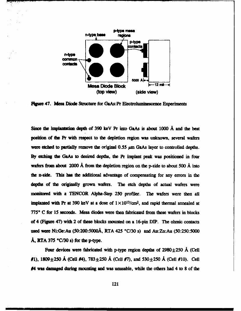
pet~ ba
Mms Dkxde BWock ---12 mi--•
(top view) (si&d view)
Fgure 47. Mesa Diode Structure for GaAs:Pr Electroumiescence Experimet
Since the implaMati depth of 390 key Pr into GaAs is about 1000 A and the best
position of the Pr with respect to the depletion region was unkmown, several wafers
were etched to partially remove the original 0.55 Am GaAs layer to controlled depths.
By etching the GaAs to desired depths, the Pr implant peak was positioned in four
wafers from about 2000 A from the depletion region on the p-side to about 500 A into
the n-side. This has the additional advantage of compensating for any errors in the
depths of the originally grown wafers. The etch depths of actual wafers were
monitored with a TENCOR Alpha-Step 250 profiler. The wafers were then all
implanted with Pr at 390 keV at a dose of 1 X 10¹³/cm2 , and rapid thermal anealed at
775° C for 15 seconds. Mesa diodes were then fabricated from these wafers in blocks
of 4 (Figure 47) with 2 of these blocks mounted on a 16-pin DIP. The ohmic contacts
used wer Ni:Ge:Au (50:200:5000A, RTA 425 °C/30 s) and Au:Zn:Au (50:250:5000
A, RTA 375 C30 q) for the, type.
Four devices were fabricated with p-type region depths of 2980±250 A (Cell
#1), 1809±250 A (Cell #4), 783±250 A (Cell V7), and 530±250 A (Cell #10). Cell
#4 was damaged during mounting and was unusable, while the others had 4 to 8 of the
121
diodft bAzCWawl. For the electrolminesce e e nts, all of the hinctional
diodes on both blocks were connected in parallel and voltages of 1.88 to 5.46 V (with
rrespodling currents of 98 to 999 mA) were applied with the resulting emission
spectra collected exactly as in the PL experiments. Unfortunately, none of the diodes
displayed Pr luminescence, but all diodes showed near band-edge luminescence of the
GaAs. Figure 48 shows the electroluminescence from Cell #1 along with
pholminescence from the surface of the diodes and from a bulk sample of the wafer
from which Cell #1 was fabricated. These results are typical of those found for Cells
V and #10. All of spectra showed clear GaAs band-edge-related luminescence in both
first and second order, however none showed any evidence of Pr luminescence. The
PL from the bulk samples displayed defect emissions which are very similar to the PL
obtained from n-GaAs:Pr (Figure 19), but the Pr-bearing region in the diode contains
a concentration of dopants an order of magnitude higher than that of the samples used
in the host conductivity type study. Apparently, the dopants present in all diodes
quenched the Pr i e. It was also possible that procedures used to fabricate
the device from the junction material hindered the Pr luminescence. The metallization
procedure used to attach contacts may introduce impurities such as gold into the Pr
implanted region, and this may also reduce Pr luminescence. However, even the bulk
material implanted with Pr was not capable of Pr luminescence. Possibly, lower
doping of the host may yet allow Pr electroluminescence to be achieved.
122

Wamveegh (P)1.8 1.6 1.4 1.2 1 0.8
cGD.:Pr p'n ~dl~1
RrA775cY5% T=3KRPO=Aftimjwidion
0 UP
0.7 0.8 0.9 1.0 1.1 1.2 1.3 1.4 1.5 1.6LLurrnescence Energ (eV)
Figur 48. Electroluminescem~ arnd Photoluminescence from GaAs:Pr Cell #1
123
.!-•," •VUl. ONJCUIlNM AM EhATIONS
-<
Each of the studies detailed in the previous chapter contributes information from
which a portrait of the excitation mechanism for Pr in AlxGal.xAs can be constructed.
Table 17 contains a summary of important findings in this work. Since Pr emissions
from Alo.14Ga.As and Alo.&GaoAs were nearly identical, but sufficient quantities
of both were not available for a complete study, their results are reported together.
The following conclusions may be drawn from the data thus far presented:
1) The behavior of the Pr PL in the RTA studies including thermal stability and
mnmber of crystal field split emission lines argues that the Pr ions occupy Ga
substitutional sites although the local site symmetry may be less than Td.
2) The SEL study showed that excitation energy as low as that of free-to-bound
transitions or bound excitons is sufficient for excitation of Pr in any of the studied
hosts. Pr-related luminescence can be excited with a narrow range of laser excitation
energies centered at 24 meV below the band-edge in GaAs. This may indicate direct
pumping to the Pr-BE energy level. For Alo.15Gao.g5As, the SEL drop-off was broader
and no below-gap maximum was observed over the range of over 280 meV below the
band-edge.
3) The temperature-dependence study gave an activation energy for Pr lines in
GaAs (22.5-28.9 meV) corresponding to the dissociation energy of bound excitons
from the Pr sites. The smaller activation energies found for the Alo0 5Gao.S5As and
Alo.3oGao.0 70 s hosts probably correspond to dissociation energy of excitons which are
less strongly bound to the Pr ion. Small activation energies of less than 4 meV may
correspond to thermal excitation of the lower cold line level to the upper level. No
evidence of differnt Pr luminescent centers was found.
124

TABLE 17
Summary of Significant Findings
Sr.Aow as A,..,ujgOAU A4.UG~bA lanmGehAs SHIMsIn mt week MY"sun strong Week nowe
PL %4+1% VM. boausi me&im noruin Very week nons R"
""o~sz -101*31=2; 1,- ii3km2 2t5.101lai 2 ý5.1013csn 2 ____
PL, pdmul TA 1*25 0 775-800 C 750-775 C 725 C 725 C() ____
MLSfremget b own Nat p SI SI nip ___
PL hteinlty Pemeer Depsinmaicm _____ suroofat__SELtOW off Euerg(*3inV) Eg4 V I-1 nmeV___
SEL Beim flop uhA 6±3 =Vi) Eg-24 =VY none ___
T-ptPuakC. AsL EIEl.E2 U.222.5meV 9.6 meV 5.6mneV too week
T-dupPamkILAft EL EII..EE2 2.Z262.9meV 1A,6.OmeV too weak too weak ___
ErD ~Iugffet quanchaPr PL qiuuichePrP K iunchedPr~t K uendiePr PL__
EffestW.C.E. rpachedPr PL qEUcIId Pr PL not tested not tested
8 hugtul.Iu..ýe no Pr Kt
4) The square root dependence of the intensity on excitation laser power
indicates that the bound exciton recombination energy may be transferred either to the
Pr ion or a free carrier via an Auger process.
5) The reduction of Pr PL in hosts occurs when the hosts are doped with donors
or acceptors, or they are codoped with other impurities is probably due to competition
with other impurities for the available exciton recombination energy. The doping or
codoped impurities were:
a) carrier-type impurities like Si and Zn,
b) other RE elements like Er, and
c) codoped impurities including B, C, N, 0, and F.
6) The intensity of Pr emission groups vanes strongly with Al mole fraction of
AlxGai..xAs. The 3F3-+3H4 emissions are strongest in Al,,GaixAs hosts with x;ŽO. 15,
125

while for GaAs and Alo.1O%,As, the sturest Pr emissions are the IG4-- 3HS
ransiion group. This behavior is abrupt, showing no gradual change. The change in
relative PL intensities between the emission groups with different hosts is attributed to
the differing bandgaps of those hosts and the interaction of these bandgaps with the
internal 4f energy states of Pr 3+.
These pieces of information and their interpretation may now be assembled to propose
an excitation mechanism for Pr in the succeeding sections.
Unfortunately, the potential application of Pr luminescence in GaAs,
AlxGa 1 xAs, and Si technology appears to be no greater than that of other REs.
Although Pr emissions at low temperatures are sharp and relatively strong, they still
fall far short of the intensity and efficiency required for use in an LED. Attempts to
increase the luminescent intensity through codoping with B, C, N, 0, and F and dual-
doping with Er were not successful and, although these tests are not completely
definitive, there do not appear to be any obvious methods to achieve strong
enhancement of Pr PL. The lack of any Pr-related electroluminescence was attributed
to the impurities in the diode, but if Pr ions are, in general, poor competitors for
absorption of exciton recombination energy, then the very impurities required to create
the p-n junction may quench the Pr luminescence. Recommendations for further
research presented at the end of this chapter do, however, present some areas for
exploration, which may contribute to the further understanding of RE luminescence.
Excitatio Mechanism Modelh
The excitation mechanism model must account for all of the data presented in
this research effort as summarized above, both for the behavior of the Pr-related
luminescence in the AIxGal-XAs hosts and lack of the Pr-related luminescence in the
silicon hosts. Examination and development of excitation mechanism models can be
126

vi into the bound excRon formation process and the bound exciton recombination
pres. flme processes will be treatd separately.
,, The p n ogical model presented in
Figure 49 shows the genera overview of the proposed semiconductor host to Pr energy
trazufr process for above bandgap host excitation. This model is entirely consistent
with the empirical data psented in this work and the conclusions drawn thus far. The
exctatio and lnmiucence process sequence is proposed as follows in 6 separate
steps:
1) Free rCFarrier.ormation Free carriers and free excitons are formed in
the host material via an external pumping process such as a laser with a photon energy
greater than the host bandgap.
2) Carricr/Ein ITnranning These free carriers can be trapped at the Pr
sites which exist as isoelectronic traps (either for electrons or holes). The exact nature
of this trap can not be conjectured until experiments are conducted to determine
whether this is a hole or electron trap (such as DLTS). The trapping of free carriers by
isoelectroni impurities (such as REs on group M sites in I-v semiconductors) is well
established. Allen's atomic potential calculations showed that semiconductor
isoelectronic bound states are probable when a large, heavy atom replaces a lighter one
(Allen, 1971:1936). Several workers have reported experimental evidence of trapping
of free carriers by REs in semiconductors including Yb and Er electron traps in InP
(Whitney et at., 1988b:2074; Lamber et al., 1990:479), Yb electron traps in GaAs
(Taguchi etal., 1990:3390), and Er hole traps in GaAs (Colon etal., 1992b:671). It is
also possible that free excitons are themselves trapped at the Pr sites and this has also
been proposed previously for RE excitation mechanisms (Lozykowksi, 1993:17760).
Quemcing processes are possible in this step which compete with the Pr ions for the
127
_Es Ift Ws 71M other trap-iag by oth -..- i-es, band-to-b and
Inh- free excsao formation and obintion and ohe-r dfcts which
allow fie carriers to de-exce.
3) ftnwd EciaImhzm fin The carrier trapped at the Pr si attracts
anohr oppositely charged carrier, forming a bound exciton. This step also depends
on tbe rcocentwat of fre carriers in the host for the supply of oppositely charged
carriers to form the bound exciton. Quenching effects for this step include ionization
or dissociation of the bound exciton through thermal energy, impact ionization by other
free carriers, or absorption of photon energy.
4) Bound Exeiton RA omhirnation This bound exciton has a finite
lifetime and recombines releasing energy at the Pr ion site.
5) E.n Aba io The recombination energy is absorbed by the
local Pr atom (or other particles). The energy conservation in this transfer is
completMe by another particle which may even be another, nearby Pr atom. This other
particle may also be a carrier excited via an Auger process. Again, the energy transfer
rate to the Pr ion may not be high. The bound exciton recombination energy may also
be transferred entirely to an Auger process.
6) ErT mincm, The excited Pr atom decays, radiating light.
This process is valid for all GaAs:Pr and AlxGa1.xAs:Pr samples for above-gap
excitation. A microscopic description of the Pr luminescence intensity can be
contructed for this model with terms for each step in the excitation mechanism, which
also accounts for each of the quenching processes listed above. A process diagram
corresponding to this complete model is shown in Figure 50 along with associated
equations and variables accounting for each step. First, above bandgap excitation
depends on free carriers which have a concentration n described by the rate equation
128

BEPus Fan.e BE Rse= mbboan
CB nprs atPrlIn ExcW Pr•Ion
PrionLmm
VB- Pr3+ WEnWVYLevel
PFguz 49. Above Bandgap Excitation Process of Pr I ninescence in AlxGa-.xAs
dn n=- -cn', (22)
where G, is the pump generation rate, l is the carrier lifetime due to deep trap
recombination, we2 is the recombination rate through exciton formation, and cO is the
recombnna•ton rate via Auger processes (Coffa et at., 1993:11787). Simple steady state
solbions to three limiting cames of this rate equation exist. At low temperatures in
good crystals, exciton recomnbmn prevails giving (Coffa et at., 1993:11787)
n (L /2 .(23)
129

Process
"11pafsl -Im ~ Wf~ft Jppa rofLIE-Z"AJr f
FigureIf 50.M PossDaa Mfo toe PrE ExFato MFEais inA1Ga..d
Pr$m 1ý " ftmgr-mn130rfi
Far high fferes, deep trap rfcombia ti dominates giving (Coffa et al.,
1993:11787)
i = G,•.. (24)
Fldnfly, for high plup rates GI, Auger processes dominate because of the large 0
Since the spectra in this effort were talmn at low temperatr with potentially high
pump rates, a combination of exciton and Auger processes probably dominates. The
square root power dependence of the PL intensity supports the strength of the Auger
PC in these materials. Coffa et al. also give a rate equation for excited Er
coerIo*, which may be adapted to describe the Pr humi escence process. The
rat equation for excited state Pr ion concentration Nfp is given by
where nba is the conof bound excitomns at Pr ions, c* is the bound exciton
reconbination lifetime, Np, is the total c of optically active Pr, fr is the
fracion of BE at the Pr ions which do not ionize or dissociate prior to recombination
(depee on the te e e), fe is the fraction of recombining bound excitons which
cxct the Pr ion (due to competition from photon emission and Auger processes), and
t id the decay time of the Pr ions whether radiative or non-radiative. The first term in
Eq (26) is the rate of excitation events which is limited by the number of already
131
Pd imi Ur iI W= it swornt by fte (1-fNf'fWN) fImor. The second tonr
ri0IS Em d-n poncees. Eq (26) depends on the free carrier conerion
trugh tb bomund •c•ciom in n an t•e form
R"'. = , f -(27)
whenrfb is a factor accounting for other processes competing for free carriers (such as
defects, other impurities, or free exciton formation). f Pr binding of excitons is not a
dominant process in the sample, then Eq (26) may be considered independent of Eq
(22) in term of the mnmber of carriers n. Thus, assuming a steady state solution to Eq
(26) and that Pr luminecee is proportional to the conceration of excited Pr ions,
the inft ity of the Pr l n e Ip is given by
N, f,fnb,I' F = I (28)
where v is the lifetime of the radiative decay for the excited Pr ion. The controllable
conditions which maximize this luminescence include increasing the nb, factor through
increasing the free carrier concentration or reduction of impurities which compete for
the free carriers. Also increasing Npr will enlarge IN, but practical limits on the
solubility of Pr ions in the lattice constrain this enhancement method.
Bamn Exeimn Recombination Process. The previous model explains the
method for Pr excitation through bound exciton recombination at the Pr site. However,
the BE energies are much greater than any single energy level of Pr, so the energy
transfer process still requires a complete rigorous explanation of energy conservation.
A review of the data suggests two possible explanations. The first is an Auger-assisted
132
process (Figure 51a), while the second is a novel Pr dual resonance process (Figure
51b). These will be examined in the context of the primary BE excitation-based model.
Pr luminesacee has been observed over a wide range of host bandgaps (1.5-2.1
eV) which correspond to similarly large BE recombination energies. This shows a
wide BE recombination energy to Pr energetic coupling range. Since the BE energies
are all much greater than the excited states of Pr3 +, a process must exist which absorbs
the remaining energy difference after exciting the 4f electrons to complete energy
conservation for this transfer. Thus, there must exist a corresponding energy
conservation process which is capable of absorbing a continuum of energies. A
possible process which fits these requirements is a transfer of the energy difference
between the BE and the Pr levels to free carriers via an Auger process (Figure 51a).
This requires yet another particle to participate in this excitation process. The energy
conservation for this model is described by
Eu = EN,. + Ew,,, (29)
where EDE is the bound exciton recombination energy which is divided between the Pr
excited state energy ENp* and the energy transferred to a carrier via an Auger process
EAW. This process must allocate sufficient energy (Ept,) to the Pr ion of at least
0.783 eV to allow the 3F3-+ 3H4 transition and about 1.2 eV to excite the Pr ion from
the 3H4 ground state to the IG4 state allowing the 1G4-+3H5 or lG4-+3H4 emissions.These then require Auger transfer energy Eger of at least 0.32 eV in GaAs (using
approxinmaely Eg-.2 eV) up to 1.287 eV in Alo.50Gao.MAs (using approximately Eg-
0.783 eV). This is indeed a very wide range of energies required for Auger-assisted
energy conservation from the BE recombination energy. This Auger-assisted process
also does not explain the switch in relative luminescence intensity between the
3F3--3H4 and lG 4-- 3Hs emission groups as the Al mole fraction x changes from
133

-e IO- d k S '-'- B "•I r-
pr3jIIPr34a) Auger Process-assisted b) Pr Dual Resonance
Figure 51. Bound Exciton Recombination Energy Transfer Processes
x-0.10 to 0.15 unless there is some preferred Auger transfer mechanism. This
problem with the Auger-assisted explanation prompted the next possible model.
The dramatic change in relative Pr luminescence intensities between the two
emission groups with Al mole fraction needs another explanation and forms the basis
for the second explanation for BE energy transfer mechanism. In the former
explantion, the BE recombination energy is split between the Pr ion and the Auger
process particle. It is also possible that the recombination energy from the bound
exciton is split between two different, but closely located Pr ions (Figure 51b).
Examiato of the Pr energy levels compared to the BE energies for each host reveals
a very interesting correlation. When taken as pairs representing double resonance of
the Pr ion energy levels, the sum of the two values of certain combinations of excited
Pr energies are close to the BE recombination energy which may explain the
luminescent behavior observed. In other words, the Pr3+ energy level pairs which are
134
best enesPetically matched to the BE recombination energy seem to correlate with the
observed changes in emission group intensity. Table 18 shows Pr3 + paired excited
energy sums which are near the bandgap energies (and presumably the BE energies) for
the hosts in this study. The differenee in the Pr energy sums and the BE energies are
small enough that lattice phonons can complete the energy conservation during the
process. Since so few of the Pr 3+ energy levels are involved in the IR emissions
studied her, the energy levels are based on the comprehensive studies of Pr3 + energy
levels in LaCl3 summarized in Dieke's book (Dieke, 1968:196). The energy
conservation of this model is described by
EMR = Elft. + E 2p•., (30)
where Elpr, and E2 ., are excited states of the two Pr3+ ions which split the available
bound exciton recombination energy EBE. For example, the Pr-bound exciton
recombination energy in GaAs would be slightly less than the 1.52 eV bandgap, which
would be sufficient and energetically well-matched to either the 1G4 + 3H5 (1.466 eV)
or the 3F4 + 3F2 (1.430 eV) excitation sums. Since no 3F4-based transitions were seen
in this study or have been reported, it is likely that the 3F4 state may be thermalized to
the next lowest level 3F3 which is only -54 meV lower in energy than the 3F4 level.
Also, no 3F2-- 3H4 emissions were seen in this study, nor have any been reported in
other Pr studies (Erickson et at., 1993). This implies that the transition from 3F2 to
3H4 may be a forbidden transition, or, at best, a very weak transition. Thus, although
emissions from 1G4, 3H5, and 3F3 to 3H4 are all possible from GaAs:Pr under this
model, the 1G4- and 3H5-based emissions are expected to be strongest because they
have the closest energy match to the BE energy, while the 3F3-based emissions will be
weaker because they are less well energetically matched to the BE energy. In fact,
135
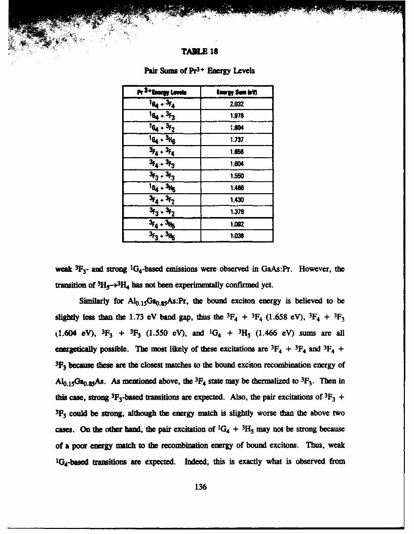
TA=L 18
Pair SUMS of pr3+ Energy Levels
pr 3 +EuWgyLW*s EmugySM V)
164 433 1.978
I6+ 3F2 _________164,31 1.804108 + 3H6 1.73731F4+34 1.8583F4 + 3F3 1.6043F3+ %3 1.5501r4 3H5 1.4863F4 + 3F2 1.430
3F3 + 3F2 1.3763F + 3"5 1.0923F3 + 3p 1.038
weak 3F3- and strong 1G4-based emissions were observed in GaAs:Pr. However, the
transition of 3H-•-I34 has not been experimentally confirmed yet.
Similarly for Alo. 1 o.s5As:Pr, the bound exciton energy is believed to be
slightly less than the 1.73 eV band gap, thus the 3F4 + 3F4 (1.658 eV), 3F4 + 3F3
k.604 eV), 3F3 + 3F3 (1.550 eV), and 1O4 + 3H5 (1.466 eV) sums are all
eneSetically possible. The most likely of these excitations are 3F4 + 3F4 and 3F4 +
3F3 because these are the closest matches to the bound exciton recombination energy of
Alo.1oG%5As. As mentioned above, the 3F4 state may be thermalized to 3F3. Then in
this case, strong 3F3-based transitions are expected. Also, the pair excitations of 3F3 +
3F3 could be strong, although the energy match is slightly worse than the above two
cases. On the other hand, the pair excitation of 1G4 + 3H5 may not be strong because
of a poor energy match to the recombination energy of bound excitons. Thus, weak
IG4-based transitions are expected. Indeed, this is exactly what is observed from
136

Al0 . 5Gao.As:Pr. Note that the 3F4 + 3F4 , 3F4 + 3F3, and 3F3 + 3F3 energetic
combinations produce a total of six excited Pr ions which will likely all emit 3F3-+ 3H4,
while 'G4 + 3H5 pair produces only one Pr ion which can emit from the IG4-+3H5
transition. This is another reason to expect more intense 3F3---+3H4 emissions than
IG4-, 3H5 emissions.
For Al.30Gao.7As:Pr, the BE energy will be slightly less than 1.94 eV. The
best energetically matched pair is IG4 + 3F2 , however, as stated earlier, this is an
unlikely process because the excitation from 3H4 to 3F2 appears to be a very weak
transition at best. The next best energetic matches are the same as those for
Alo. 15Gao. 5As, but with a greater energy difference. Thus, similar emissions to
Alo. 15 Gao.85As are expected, but substantially reduced in intensity, just as have been
observed. This same effect occurs with Alo.50Gao. 50As, with even greater reduction in
the emission intensities as is also seen.
The exact solution to the issue of energy conservation in the BE energy
absorption process by the Pr ions may not be exclusively either of the two preceding
models. It seems likely that both of these processes occur to some degree, since
neither seems to be a completely satisfying model for this BE energy recombination
step.
Lack of Pr Luminescence in Si. No luminescence from Pr was seen in Si hosts
and this may result from any number of potential quenching effects which have been
identified in this study. First, the relation of Pr to silicon is fundamentally different
from that of 111-V materials since silicon is a group IV elements. Thus, trivalent Pr in
a substitutional site is presumed to behave as an acceptor-like impurity. Pr luminescent
centers are believed to be substitutional and isoelectronic in the AlxGal-xAs hosts,
while Pr may be neither in silicon. Also the low temperature bandgap of silicon
137
_4, W- -TI" wW
(1.17 eV) h much less than that of any other host tested in this study
(1.52 to 2.07 eV), along with being indirect (although weak Pr emissions from the
indirect gap A!0.G.aSAs host were detected). This low bandgap is, in fact, less than
the 1G4 excited state of Pr3 + (-1.2 eV) eliminating the possibility of pumping the
ground-state 4f electron to this level. Under the dual-resonance model for Pr
excitation, there is only one energy pair containing 3F3 and one pair containing 3F4
which have an energy less than the recombination energy of a bound exciton in silicon,
i.e., the excitation of 3F 3 + 3H 5 (1.038 eV) or 3F4 + 3H5 (1.092 eV). Additionally, only
p- and n-type silicon host materials were tested. The study of Pr-implanted in to n- and
p-type AlxGai.xAs hosts has shown evidence that, in general, impurities have a strong
quenching effect on Pr luminescence. Finally, the excitation laser penetration depth is
not well matched to the Pr implantation depths in Si, as was noted earlier. It seems
that Pr is not well suited for use as a luminescent material in silicon, although it is not
possible from the evidence in this study to positively discriminate between these
possible reasons.
Comparison with Er and Yb Excitation Models. Extensive research has been
conducted on emissions from both Er and Yb in semiconductors and well-developed
excitation mechanism models were put forward. These models do differ from those
presented here for Pr, and none has presented a dual-resonance model involving
simultaneous excitation of two RE particles. In general, the availability of DLTS data
allows more specific details to be part of these processes.
Colon et al. have discovered that Er forms at least two hole traps in GaAs (at
35 and 360 meV above the VB) and outlined a very specific set of steps for Er
excitation for laser excitation energy greater than and smaller than Eg of the host
(Colon et al., 1992b:674). For the above-gap laser excitation, free holes are trapped,
138
which then form bound excitons whose recombination transfers energy to the Er ion via
an Auger energy transfer. For laser excitation less than the bandgap, electrons at the
trap are excited to the CB leaving behind a bound hole which subsequently recombines
with an electron transferring its energy to the Er 4f-shell. One difference between this
work on Er and that presented here for Pr is the existence of deep traps which were not
found through temperature dependent PL measurements for Pr, but can not be
completely ruled out until DLTS is performed on GaAs:Pr.
Takahei and Taguchi have worked extensively on the Yb in InP, and have
shown that Yb forms an acceptor-like electron (AE) trap at about 30 meV below the
CB in InP (Takahei and Taguchi, 1992:643). This AE trap level is located close to the
CB, but is acceptor-like in that it becomes negatively charged by capturing an electron
from the CB. The captured electron was shown to exist outside the Yb 4f shell
maintaining the Yb3+ ion, thus showing that the AE trap acts as an isoelectronic
electron trap. Since the Yb center is isoelectronic, there is no long range coulombic
force such as that of typical shallow donors and acceptors. Thus the trapped electron is
localized around the Yb site and recombination of this electron with a hole will result
in a high transfer rate of the recombination energy via an Auger process to the 4f
electron of Yb. Energy conservation in this model by Takahei and Taguchi is invoked
simply through the Auger process, presumably through a free carrier. Again, as
proposed for Pr, the basic energy source for Yb is trapped electron-hole recombination
whether captured separately or as an exciton.
Recommendations
Several extensions of this research effort are possible which would themselves
greatly contribute to the increased understanding of Pr luminescence. These include
experiments to:
139

(1) Investigate the dual resonance model of excitation of two Pr ions via further
Inmuce e m -a--ren-ents using different semiconductor hosts with proper bAndgap
energies. Since the model requires pairs of Pr ions, the intensity of Pr emissions
should be proportional to the square of the Pr concentration for low implant doses.
(2) Conduct DLTS and temperature dependent Hall effect measurements on Pr
in various hosts to determine deep trap levels associated with Pr in these hosts. This
would require higher Pr implantation energies (MeV range) to cause deeper
implantation depths to fabricate p-n junctions or Schottky diodes for DLTS
(3) Conduct SIMS measurements to determine the actual Pr density profile for
in the samples used in this study.
(4) Continue work on EL by constructing and optimizing a proper Pr-based
diode utilizing well-understood host semiconductors. The most promising
semiconductors are low-Al fraction (x -0.15) AlxGal.xAs hosts with low level doped p-
n junction. PL tests should be run on any bulk junction material prior to diode device
fabrication to verify that the implanted junction material has reasonably strong Pr
emissions.
(5) Conduct temperature dependence PL and SEL experiments on Pr-Er dual-
doped semiconductors to better understand the processes in these materials. Hopefully
a new Pr-Er complex will manifest itself with promising results of strong PL.
(6) Conduct more PL on Si:Pr annealed at lower temperatures than those
attempted in this effort (< 750 °C).
(7) Compare the band-edge emissions intensity with that of Pr emission as a
function of Pr concentration providing some insight into the 4f excitation mechanism.
140
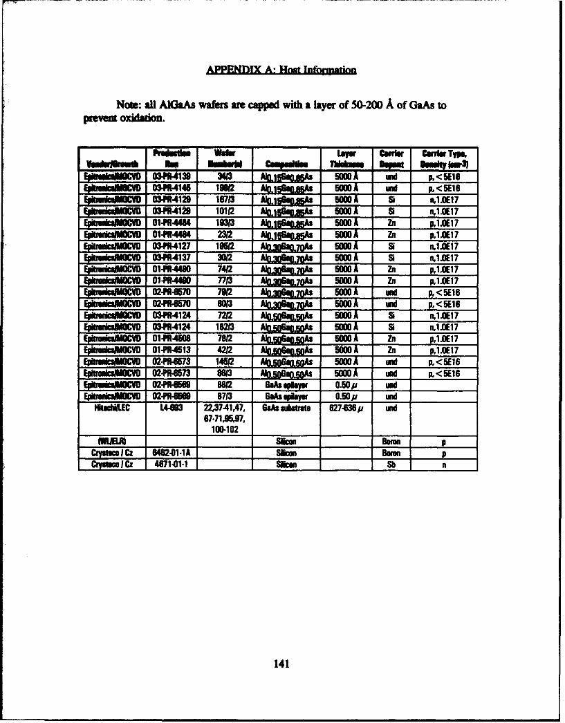
APPNDX eHos nfrato
Note: ali AIGaAs wafers are capped with a layer of 50-200 A of GaAs toprevent oxidation.
Prdut~. WNWa tay Crd CCaria Type.kvuW*W*ON so b0bsW 111.1" mkm DO S- 4W
%' A 03FR414 m91 At&X W'UT ud p. <5ElS
SHbNM 03aP4129 16713 ftj1jjmm 5O Si n,1.0E17.~fonsM 03-PR4120 10112 AIjG~5 5000 M n.1.0E17
EO-I W 14PR4484 lo3w Ahsos 50=0 Zn p,1.0E17OEI *D 1-PR.4484 2312 Aklf~ 500 Zn pI.1.117
s* WOD034PR4127 19512 At~ftM p 50M 1 Mi n.1.0E17Ep MCD034IR4137 3012 N~to 5000 ai n.1E17Ep MM 01.f4IMM 7412 ftp,1 500 Zn pI.1.117Fj ACD01-PR4M8 7713 ft f.0 5iAT- Zn pI.1.117t. A 02..PR-OM7 7912 AI~t7~ 5M A id P. <5E164, 0M 024'414EN 8013 ft36M7~ 500 mid p. <5E164 MC 03-PR4124 7212 MU~&k 50 A~J Mi eI..E17
Fitri*AOCDM 034PR4124 18213 AIijGWU SiW n,1.0E17Ep!MM 01-PR4508 7812 500 A Zn p,1.0E17
OPOI WOV 1.R4*"M3 4212 ft jgtm 500 Zn p,1.0E1702.P4M53 14612 AIf.o 5W A ud p. <5E1602-PR-8673 8613 A j.W M MWA uid p <5E 16
AI 02.R.56 8812 GaAs qisyor 0.50/ p Mid _____
Ep` WAuicIMCD 024Pr85 8713 GaAs ~plae 0.50j p md _____
NiAdiWLC L4.803 22Z3741,47, Gafts uahtrats 627 4638p mid67-71,95,97,
_______ _____ ~~100-102 _ _ _ _ _ _ __ _ _ _
MUM _ _ _ _ _ _ Boro -P
CrgutucIlCz 6420.A____ Slice BoronCr~m cI Cz 47011___ Slke. ____ Sbn
141
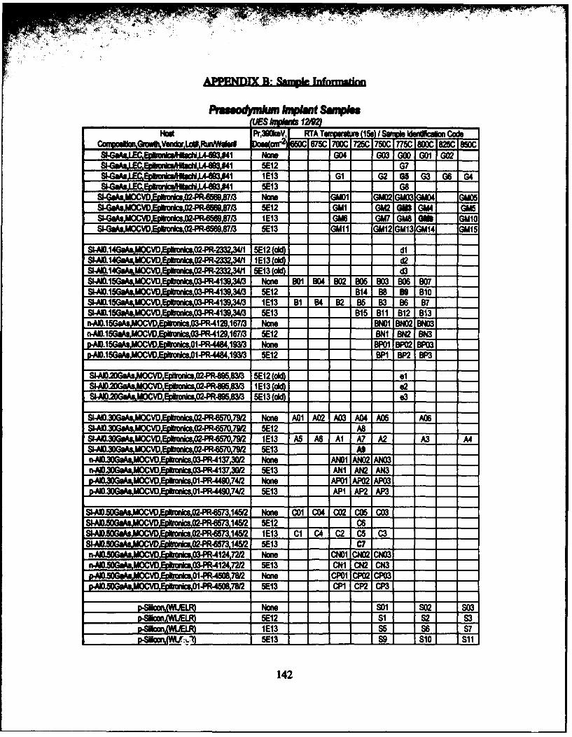
AB M B- Smmi *-,.....- a *- -
4 .odn kq WSqk
Host Pr,3SkV, __Tu.(15s)/ umi wnhcean cod_Canag~,.GtVGWorL*.Rmw~M" an m- 6750 6 7000 725C 750C 775C 80CC 825C OMC
S14.'A I EC~rxh mI*,Uk8B3M-M 1 Nowe G _04 G_ 03 G00 601 G02 _
SIWinA=.!EpCwuWb dd Ma. L44B3MI 5012 ___ __G7
SWGAM LEC ev~a**uf~htKM.L44"3#1 1E13 GI1 _ G2 05 63 G6 G4SW.G.LEC,Evbnno*iHbcuhIL4-693.41 5013 68I
SG."uMOVD.EvbosMs.2-PkR.8569Ar None -GMill G 'M02 o43 GLID4 GU05SW~AMMOCVD.Evkonlc02-PR4569A7/3 5012 ____GMI - M.2 IGO 65.4 GM5SWAs.MOCVC.Evohm ks,02-PR4M6987/3 1E13 ____GUS GW I GMS GUS GUIS~S&..sUMOCVDEvaon s.02-PR-M698713 SE13 - GM11 GM12 GU13 GM.14 - M.15
IMO.14C*As.UOCVD.Ev` 1'rs02-PR-233Z34/ 50 -d - - -di_-StMW.i4U~4OCVDa*&nbArd2-PR-233234/i W3~J -ol QSMD.14G.'&UOCVD.Eplhnlcs.024-PP-23234/1 50 -ok QSIM 15GaAsMuOCVDEv~vrnb,03.PR-41~34/3 None 901 904 902 905 90 W1906 907SI-AI.lSCaAsMOCnD~csf,03-PR4139,34i3 5012 B_ 14 88 M8 810SIM.AfllGes.MOCVD.EvloNlrcs.03-PR-4139.34/ 1E13 B1 B4 182 55 93 86 87SIM.A)i5Ca,&MOCVDEcoronxc,03-PR-4139.34/3 503 ____ 815 811 912 813ný15G.&uMOCVD.~nies3.P 4129,167r3 Nome __( __ NOl 2 DN031ni-MO.i5GUOWCVD.Eg fnc.0PR-4129.167/3 5012 1_- - _ SNI 8142 8143 - -
pAE.15G-aAs.UOCVDE1Ioncs01-PR-4484,193/3 None I__ ___ l 8P1P02 9P03PM-AO15G~ae.OCVD,Evllrnlcs,01-PR-4484,193/3 5012 B__- - __ PI BP2 9P3 - -
SWMI20G.UsOCV.D 9pvOs2-PR-895,8WJ 502~ -dc - -el_
S.W.23G.~s.OCYD.Evtronics,02-PR-885,83/ jE1(jd 9 2SIA0.2DG.as.MOCVD.EvbonlmW,0-PR-895A3/ 50 -ok 93
SlM.30GasALMOCVDWp02.PR457,7W~ None A01 A02 A03 A04 A05 A06S)AE)MG&As.UOCVDEWNIICS02.PR-6570.92 5012 AB _
S&AI.30G.OAs.UCVD.Epvih'ncs,02-PR4670,7W IE13 A5 AS Al A7 A2 A3 A4SIAW30G.'.s.OCVD.E8Arcnics02-PR467079I2 5013 __AS I_n-AIO3OGaALMOCVD.Evlranlcs03-PR4137=3/ Nonem ANDl AN02 AN03nAGO3OG~i.UOCVD~vwh m Om-PR137,Wt 5013 _ANI IN AN31p.AI3OGA.UOCVD.Evkoics01-PR-4490,74/2 Nonem AP01 AP02 AP03pAI).0G.es.MOCVD.Evbanics.01-PR-4490,74/2 5013 ____API AP2 AP3
Uk="OCVIDEvknc".02-PR4M7,145f2 None 001 C04 002 005 C03 - - - -
SI.3.0GWsUOVD.Epftnics,02-PR-M7,14512 5012 1__ 06s _
SI.AIO JOVD~nis02.PR4573145/2 1E13 Cl 04 02 I05 C3S02-PR45DAwd.Q 73 45l2 5013 ___C7 _
mASOGaAMCD.vkncs0- M41471 Nonw - NOI CN02 CN03n.AI0.5G.'AUOCVD.Evpbm"c03-PR4124.72r2 5013 ___ NI CN2 CN3pMAG&W=M ftV.Evonim 01-PR4508,7M2 None ___ POl CP02 CP03pAIOSOAsUOCVD.EvI~onlcs.01-PR-4508.78 5013 ____ ___O C P2 CP3
p.SqcanIWULR)a None -s 9 02 S03DM.SlIOf.(LELR) 5012 1_ __ SI S2 S3pSIkoonMJELR) 1E13 1_ __ 5 98 97
~f r3j5013 1_ 1_ 99 910l 911l
142
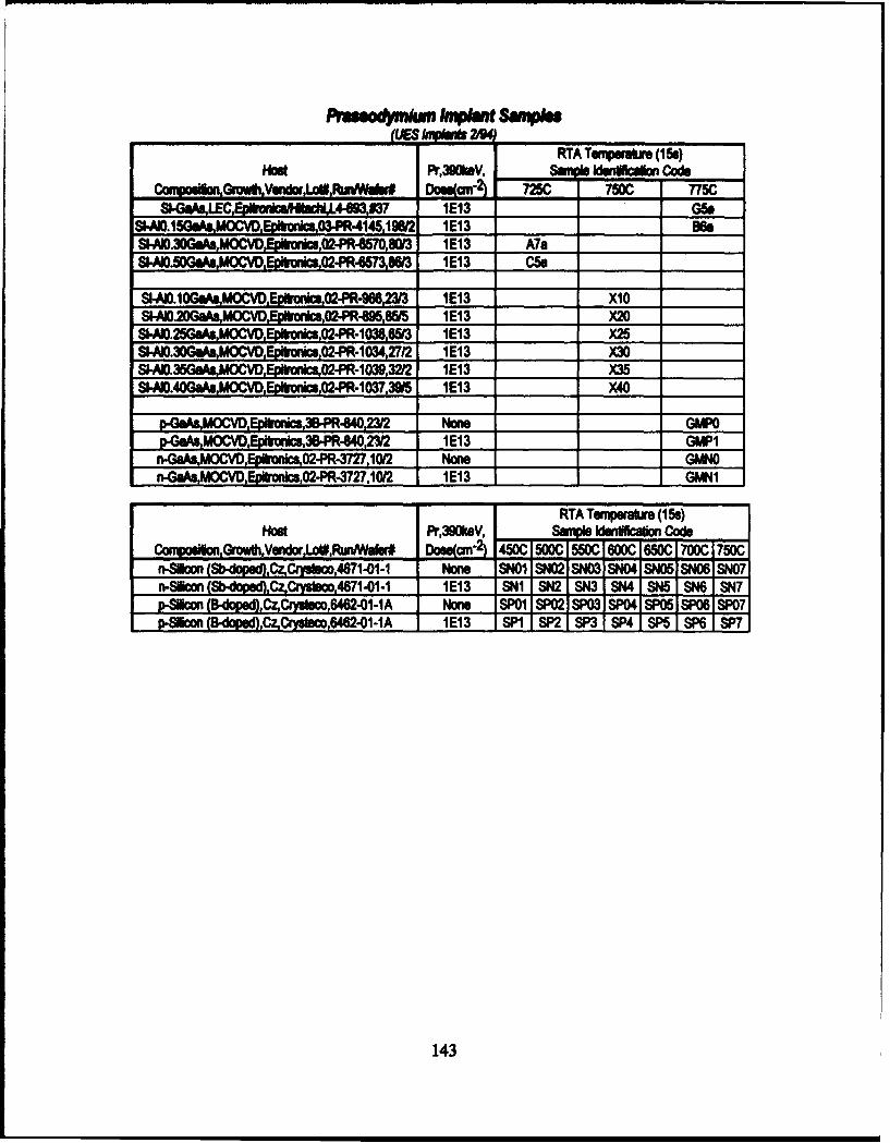
RTA ToemprAi (15.)Hodt PrO~MV, _____ Id, dreion Cods
CanipuIobn.GrwMVwidor,LoSIAmW*# 7m5 7w0C 775CSIGa.jlECreA onkcsA lbhLL4-693.D37 IE13 G50
&IMO.15GOA'MOC.VDhiuO3P 145,19W2 E13 we__ ___ 6SkMO.3GO~A,MOC2VD,E*Onics,02-PR-457,O,83 ME3 Ala _________
%MAI.50G&4A~MOCVD,EvIh m"c,02-PR457366I 1013 C50 __________
SI-AIO.1OGMu)OCVDEvph'nics,02-PR-96,2313 1013 _____ X1O ___
SI-A1.2DCe4k.MOtVD,EpI~NmcsO2-PR-6S,85I5 1E13 _____ X20 _____
SI-AO.25Ga4sMOCVD,Epibonrcs,2-PR-1038,65&3 IE13 _____ X25 _____
SMM.30Ge~sMOCD,Epihnics,02-PR-1034,27/2 1013 ___X30 ____
SI-AI GO. MOCVD 0oncc2-PR-1039,32/2 1E13 ____w 3
_ _ _ _ _ _ _ _ _ _ _ _ __R840 No GMPO_ _ _ _ _ _ _ _ _ _ __,3-P-80,3/ I1 GMPI
n-GaMs,MOCVD,Epihnics,02-PR-3727,1012 Noe1 ____ ___ GMN1
RTA Temperature (I 5s)Host Pr,3B9koV. San~vb Wwticaoion Code
Cvompsio,Growlh,Vordor.LoWntwaM" Doc- 450CT 500C I550C1 600C 650C 700C 1750Cn-Slco (Sb~doped),;zýCryssoo,4671-O1-1 None 81401 jSNO2 SNO3j 81404814581M068147n-Skion (Sb~fot4&&CGysbwo,4671-01-1 1E13 8141 812 SN 813114 8145 816 8147p-Skco MB~oped),CzCiyalsc,6462-01-1A Noe SPOl SP02I WP3 SP04 WMSPO P06 SP07p-Skcon (B-dopeMCzGryusco,6462-01 -lA I1E13 _SPI , P2, I P3 .1 8P4 , P5 . P6 8P7
143

-7-- -; -j1771.111ýAMESffdt 120=92 A 1I 3J _________
(UES 12192 (UES.11/93) RTA Taiiperdtax (1 5.)Hodt Pr,39CkeV, ErIMeV, kdendlcion Cods
Conipoinilo,Gmft,Vunw'.rLonRwMidst Dmc bOGm 70 750C I S0C 85OWCSW-iAsLEC,Evibon m at~bAL4.693,91 Nome 1E13 GEl GE2 IGE3 GE4
SIGAjE.vvnW&uHltah, L44603,01 None 5E13 GE5 GE-6 GE7 GE8SW.Giaft,LEC, " crnlcmHbwtI,14-63,#41 1E13 1E13 GOI GD2 GD3 G04SI-Gk,LEC,Evibm qxicwMla,L4493,f41 1013 5013 G05 GD6 GD7 G08
S.MO.15GAM,MOC1VD,Epifonios,03-PR4139,34/3 None iE13 BEI 8E2 . E3 SE4SI-PJO5GaAs,MOC VD,Epihnics,03.PR-4139,3413 None 5El3 BE5 BE6 8E7 BE8SI-AI.15GaAs,MOCVD,Evpbonics,03-PR-4139,34/3 IE13 1E13 901 802 803 804SI-AI.15G.M4kMOCVD,Evkihni,03-P4139,34/3 5013 5013 806 806 807 80
SI-NO.3GaksMOCVD,Evib'onics2-PR-6570,79/2 None 1E13 AEI AE2 AD3 AR4SI-AM.30Ga04,MOCVD,EpIonjcs,02-PR657o,79/2 None 5013 AE5 AE6 AE7 AE8SI-AI.3po~s,MOGVD,Evhi~'ncs,02-PR-667O,79/2 1E13 1E13 ADl AD2 AD3 AN4SI-AI.Oas MOCVD,Whncs02-PR-WOlO792 5013 5E13 AD5 AD6 ANl AD8
SI-AI.5OGaMMOCVD,Epwitro,02-PR-663,145/2 None 1E13 CEl CE2 CE3 CE4SIAI.5OGaos,MOCVD,Epkitrns,02-PR-653,145'2 None 5E13 CE5 CE6 GE7 CE8.SI-O.5OQaks,MOCVD,Epifonics,02-PR-6573,145/2 1E13 IE13 CDI CD2 MD3 CD4SI-AJOSOPeAMOCVD, ois02-PR-8673,l4512 5013 5E13 CD5 CD6 CD7 CD8
144
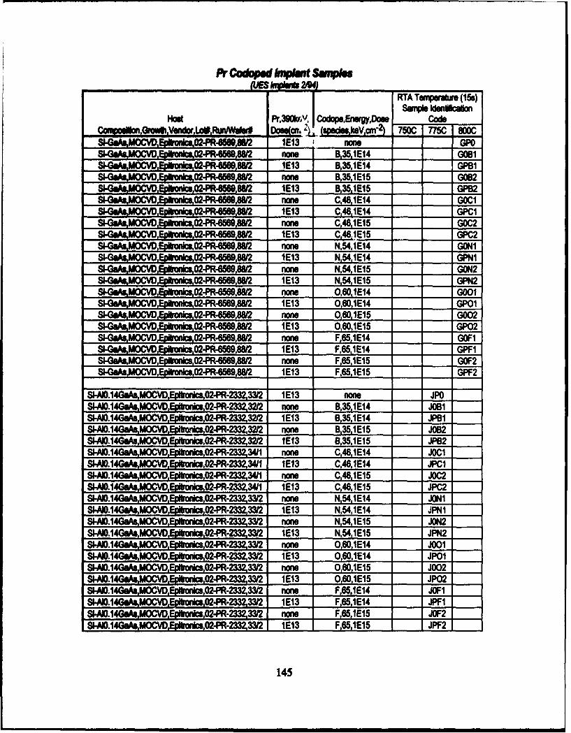
Pr Codoped Inwbsn Sawiipn
I ~RTA Turmeraare (15.)
Hodt Pr,39&,%jY Codope.BrgyDooe codeCanGuI w lb*,.Ywd,LOIRunrW# Docf L~WWa 750C 775C B0CSW-fMOCVD 02-nmMPR-NW 2W 1E13 none GPO
SI4g@sMOCVD,Epib'onmlcs,2-PR-6669862 nowe B,35,1E14 G0B1S4W^~sMOCVD.Evpb'nlcs02-PR-W698W/ 1E13 8,35,1E14 GPBI
SIGa.MCVE~hAlcs,02-PR-M,666.2 none B,35,1E15 08M-aMOCVD E~wx02-PR-666BW2 1E13 8,35,1E15 GPB2
S44.AsMOCVD.EI c,2-R69801 none C,48,1E14 GOCISI-a&AAMOCVD ,EA mNOnc,2-PR4M6,86/2 IE13 C,46,1014 GPCI
SIG.s,0 VDvIonics2-PR-656.8W/ noneC48m1 GOC2SI4A.MOCVD,Ep~onlcs,02-PR-666.882 IE13 CA1E15 - GPC2
02-R-669 8/ none N5,E4GONISI-GafjM0CVD,Ep~onrc02-PR669,W IE13 N,54,1014 GPNISI-G.MMOCVD,Evka.*s.02-PR456088/2 none N,54,iE15 GON2SI-GAsMOCVD,Ep~ftrOnl2-PR-656,882 1E13 N,54,IE15 GPN2
0f~nk,2-PR-M8W6,8/ none 0,60,1E14 00%I4AMOCVD,EpIonics,02-PR4M6,88/2 1E13 0,60,1E14 GP01SI-a&4kgMOCVDEon,2P468/ on 0,60,1015 G002
SAMOCVDE nis02-PR-65688/2 1E13 0,60,1015 GPO2SI-GaAMOCVD,Evitonims.2-PR-656,8&2 none F,65,IE14 GONiSI-GAsMOCVD,Ev~b'nls,02-PR-6569882 IE13 F,65,1E14 I__ GPF1SI-GAkMOCVD,Ei*Okics,02-PR-666,882 none F,65,1E15 GOF2SI-GaAsMOCVD,Ep~imoic,0-PR4WM6,8W1 IE13 F.65,1E15 GPF2
SlM-AO14G.au,MOCVD,Evbonlcs,02-PR-233233/2 1E13 none JP0SM-A1O.14GAsMOCVD,EpI~onics,02-PR-2332.32/2 none 8,35,1E14 JOBISINO-14GaksMOCVD,Epib'nlS.02-PR-2332,321'2 IE13 8,35,1014 JPBISIM0.l4CaAs MOCVDE ws02-PR-2332,32/2 none 8,35,1E15 JOB2
SI-I014G~,MOCVD,Evitonics,02-PR-2332,32/2 I~383,E13 PBSI-AJ014GaAMOM0CDEvibankcs,2-PR-233234/1 none C,46,IE14 JOCiSI-AI.14Ga&sMOCVDEvlfonics,02-PR-2332,34/1 IE13 C.48,1E14 JPCISI-AJ.I4G9sMOCVD,Evptoeim,02-PR-2332,34/1 none C,46 IElS JOC2SI-AI.14G MOCVD 0ftim2-PR-23 34/1 lEl3 C,46,1015 JPC2SI-MO.14Gfas,MOC VD,Evkonics,02-PR-23Z33/2 none N,54,1E14 JONISI-O.14GaAs,MOCVD,Eplkoncs,02-PR-2332,3312 IE13 N,54,1E14 JPNISI-N.14GaAs,MOCVD,Epfonics,02-PR-2332,33/2 none N.541IE15 JON2S-MO.14GaAsMOCVD,Epnitrns,02-PR-2332,33/2 IE13 N,54,1E15 JPN2SI-NO.I4G2sMOd VD.Eplrcnlc,02-PR-233Z33/2 none 0,60,1014 J~oISI-NO.l4GaMs,MOCVD,EpOhnics,02-PR-2332,33/2 10E3 0,60,1E14 JPO1SI-MO.14Gats.MOCVDEpltrnls27-P-2332,3312 none 0,60,1015 J002SI.O.14Ga4sMOCVD,Ep~honlcs,02-PR-2332,33/2 1E13 0,60JE15 JP02SIMO.14CGas,MOCVD,Eplhnlc,02-PR-233Z3312 none F,65.1E14 JOFISI-AI.14CG.As,MOCVD.Evllrnics02-PR-233233/ 1E13 F,65,1E14 JPFIS4MO.14GinAsMOCD,Epb'onkcs,02-PR-2332,33/2 Inone I F,65E15 JOF2%IAI.l4GoAs,MOCV, pbonc,2-PR-2332,3312 1E103 1 F. lEl5 JPF2
145
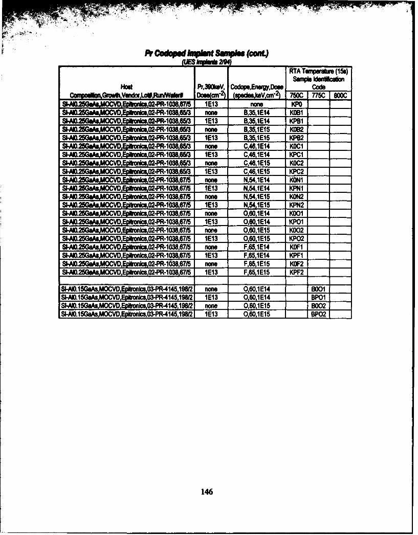
Pr Codopd I..t SWOp~s (cwi)
RTA Twnipwerau(15e)-ui wwdflcion
modt Pr,3MOkV. CodopsEiwgyDoes CodeCwnosfonGrowU'Vedorlo. (moRunIW* m 75O-Cr775C S00C
Sk.MO25GaAWMOCVD,Ec 6 m *s,02-PR- 038.6715 1E13 none KPOSMIO.25GAsuMOCVD.Evbonics,02.PR-1038,65I3 none 8,35,1E14 1(081SI-AW25GeosM0CVD,EIpkanicsO2-PR-1038,65W3 1E13 B,35,1E14 KPB1S-M).250e4sMOCVD,Evltonics,02-PR-10386.663 none 8,511 K082SI-IO25G-AksMOCVD,Estpornlcs,02-PR-10M8.65/3 1E13 B,3-5 IElS5 KP82.,%M W25G&4&MOCVDEp~bonicO2-PR-138,603 none C,46,1E14 KOCI
SAO2GAsMOCVD,EvpbonlciA2.PR*1038,6513 1E13 C, JE14 KPC1SI-MO G~sMOCVD Eftt02-PR-I 36W63 none C,46,1E15 KOC2SI-O.25GAsMOCVDEvihonics,02-PR-1038,6W3 1E13 C,46,1E15 KPC2SI.AIO.25GAMOCVD.Ea~nlcs,02-PR-1038,6715 none N.54.1E14 KONISI-MIOZGaAuU0CVDEv~knics,02.PR-1038,67j5 1E13 N,54,1E14 KPNiS4.'J25GmkMOCVD,Eplim nIrg,02-PR-1038,67/5 none N,54,1E15 KON2SIM25CeAuMOCVDv konincs,02-PR-1038,6715 1E13 N,54, E15 KPN2SI.I.25G@AaMOCVD,Evpfrn~m,02-PR-1038,6715 none 0,60,1E14 1(001
S&O2GAsMOCVD,Eplbuilcs,02-PR-1038,67/5 1E13 0,80,1E14 KPOISI- 25GaAsMOCV .Epltroic,02-PR-1 038,67/5 nope 0,60,1E15 K(002SI-AI.25Ga sMOGVD,Epltrnlcs,02-PR-I 038,6715 1E13 0.60,1015 KPO2SI-AI.25GaAsMOCVDEgpb'ndc,02-PR-1038,67/5 none F,65,1E14 KOFISI-AIO25GaAs,MOCVD,EpwirOnc,2-PR-1038,67/5 1E13 F,65,1E14 KPFIS&AI25GaAs,MOCVD,EvI~onkc,02-PR-1038,67/5 none F,85,1E15 KOF2 _ _
SI-AI.25GeAsMOCVD,Epllroics,02-PR-1038,67/5 1E13 F,65 1E15 KPF2
SIM0.15Ga~,MOCVD.Ep~imok,03-PR-4145,19612 none 0,60,1014 .8001S-MO.15GaAsMOCVD.Epllrnlcs,03-PR-4145,198/ 1E13 0,60,1E14 EP01ISI-AI.15GaMs,MOCVD,EiOhnics.03-PR4145,196/2 none 060,IE15 B_ 002ISI-MO.ISGas,MOCVD,Epilonics,03-PR-4145,19/21 1E13 I 0,60,1E15 ___ P02
146

ImTImOGRAPHY
MAchi, Sadao. "GaAs, ALAs, and Al1Gal.1 As: Material Parameters for Use inResearch and Device Applications," Journal of Applied Physics 58(3): RI-R29(1 August 1985).
Alferov, Zh. I., V. I. Amosov, D. Z. Garbuzov, Yu. V. Zhilyaev, S. G. Konnikov, P.S. Kop'ev, and V. G. Trofim. "Investigation of the Dependence ofLuminescence Emitted by n- and p-type G8PxAsI-x and AlxGat-xAs SolidSolutions on their Composition," Soviet Physics-Semiconductors 6(10): 1620-1625 (April 1973).
Allen, J. W. "Isoelectronic Impurities in Semiconductors: A Survey of BindingMechanisms," Journal of Physics C: Solid State Physics 4:1936-1944 (1971).
Arflken, George. Mathematical Methods for Physicists, 3ed. San Diego: AcademicPress, 1985.
Aspnes, D. E. and A. A. Studna. "Dielectric Functions and Optical Parameters of Si,Ge, GaP, GaAs, GaSb, InP, InAs, and InSb from 1.5 to 6.0 eV," PhysicalReview B 27(2): 985-1009 (15 January 1983).
Aspnes, D. E., S. M. Kelso, R. A. Logan, R. Bhat. "Optical Properties of AlxGai.xAs," Journal of Applied Physics 60(2): 754-767 (15 July 1986).
Bantien, F., E. Bauser, and J. Weber. "Incorporation of Erbium in GaAs by Liquid-phase Epitaxy," Journal of Applied Physics 61(8): 2803-2806 (15 April 1987).
Benton, J. L. et al. "The Electrical and Defect Properties of Erbium-implantedSilicon," Journal of Applied Physics 70(5): 2667-2671 (1 September 1991).
Benyattou, T., D. Seghier, G. Guillot, R. Moncorge, P. Galtier, and M. N. Charasse."Optical Studies of Erbium Excited States in GaO.55AIO.45As," Applied PhysicsLete 60(3): 350-352 (20 January 1992).
Benyattou, T. D. Seghier, G. Guillot, R. Moncorge, P. Galtier, and M. N. Charasse."Time-resolved Photoluminescence Spectroscopy from Erbium-dopedGa0 .55A. 45A," Applied Physics Letters 58(19): 2132-2134 (13 May 1991).
Bimberg, D., M. Sondergeld, and E. Grobe. "Thermal Dissociation of ExcitonsBounds to Neutral Acceptors in High Purity GaAs," Physical Review B 4(10):3451-3455 (15 November 1971).
147

Boer, Kari W. Srvey Of SmcduorPhysics Volume ff. Barriers, Junctions,&oaces, and Devices. New York: Van Nostrad Reinhold, 1992.
Boer, Karl W. Survy of Semiconductor Physics: Electrons and Other Particles in BulkSmiconductors. New York: Van Nostrawd Reinhold, 1990.
Brilgel, Werner. An Introduction to infrared Spectroscopy. New York: Wiley In,1962.
Casey, Jr., H. C. and M. B. Panish. Heterostructure Lasers. New York: AcademicPress, 1978.
Coffa, S., F. Priolo, G. Franz6, V. Bellani, A. Camera, and C. Spinella. "OpticalActivation and Excitation Mechanisms of Er Implanted in Si," Physical ReviewB 48(16):11782-11788 (15 October 1993-11).
Colon, Captain J. E. Luminescence Study of Ion-Implanted and MBE-Grown Er-DopedGaAs and AlxGa•.As. PhD dissertation. School of Engineering, Air ForceInstitute of Technology (AU), Wright-Patterson AFB, OH, December 1992a.
Colon, J. E., D. W. Elsaesser, Y. K. Yeo, R. L. Hengehold, and G. S. Pomrenke."Excitation Mechanism of the Erbium 4f Emissions in GaAs," MaterialsScience Forum 83-87: 671-676 (1992b).
Colon, Jose E., David W. Elsaesser, Yung Kee Yeo, Robert L. Hengehold, andGernot S. Pomrenke. "Luminescence Study of the Intra-4f Emissions fromGaAs:(Er+O) and Al.GalxAs:(Er+O)," Mat. Res. Soc. Symp. Proc. Vol.301: 169-174 (1993a).
Colon, J. E., D. W. Elsaesser, Y. K. Yeo, R. L. Hengehold, and G. S. Pomrenke."Enhancement of the Er3 + Emissions from AlGaAs:Er Codoped with Oxygen,"Applied Physics Letters 63(2): 216-218 (12 July 1993b).
DiBartolo, Baldassare. Optical Interactions in Solids. New York: Wiley & Sons,1968.
Dieke, Gerhard Heinrich. Spectra and Energy Levels of Rare Earth Ions in Crystals.New York: Interscience Publishers, 1968.
Dmitriev, A. G., L. F. Zakharenkov, V. A. Kasatkin, V. F. Masterov, and B. E.Samorukov. "Electroluminescence of Ytterbium-doped Indium Phosphide,"Soviet Physics-Semiconductors 17(10): 1201 (October 1983).
148
Emen, H., J. Wagner, H. D. Muller, and R. S. Smith. "PhotoluminesceceExcitation Measurements on GaAs:Er Grown by Molecular-beam Epitaxy,"Journal of Applied Physics 61(10): 4877-4879 (15 May 1987).
Ennen, H., G. Pomrenke, A. Axmann, K. Eisele, W. Haydl, and J. Schneider. "1.54-pm Electroluminescence of Erbium-doped Silicon Grown by Molecular BeamEpitaxy," Applied Physics Letters 46(4): 381-383 (15 February 1985).
Ennen, H., J. Schneider, G. Pomrenke, and A. Axmann. "1.54-!nicron Luminescenceof Erbium-implanted I11-V Semiconductors and Silicon," Applied PhysicsLetters 43: 943-945 (15 November 1983).
Erickson, Lynden E., Usman Akano, Ian Mitchel, Nelson Rowell, and Aiguo Wang."Photoluminescence Spectra of Trivalent Praseodymium Implanted in Semi-insulating GaAs," Journal of Applied Physics 74(4): 2347-2353 (15 August1993).
Favennec, P. N., H. L'Haridon, D. Moutonnet, M. Salvi, and M. Gauneau. "OpticalActivation of Er3+ Implanted in Silicon by Oxygen Impurities," JapaneseJournal of Applied Physics 29(4): L524-L526 (April 1990).
Favennec, P. N., H. L'Haridon, D. Moutonnet, M. Salvi, M. Gauneau, and A. C.Papadopoulo. "Implantation of Erbium Elements in GaAs and RelatedCompounds," Inst. Phys Conf Ser. No. 106: Chapter 5, Paper presented at Int.Symp. GaAs and Related Compounds, Karuizawa, Japan, 1989: 330-338.
Gippius, A. A., V. S. Vavilov, V. V. Ushakov, V. M. Konnov, N. A. Rzakuliev, S.A. Kazarian, A. A. Shirokove, and V. N. Jakimkin. "Defects and OpticallyActive Transition and Rare Earth Elements in III-V and H-VI Compounds andDiamond," Materials Science Forum Volumes 10-12: 1195-1200 (1986).
Haydl, W. H., H. D. MUller, H. Ennen, W. K6rber, and K. W. Benz. "Ytterbium-doped InP Light-emitting Diode at 1.0 pm," Applied Physics Letters 46(9):870-872 (1 May 1985).
Hecht, Eugene, and Alfred Zajac. Optics. Reading, Mass.:Addison-Wesley, 1979.
Isshiki, H, H. Kobayashi, S. Yugo, T. Kimura, and T. Ikoma. "1.54 pAmElectrolminescence by Electron Impact Excitation of Er Atoms Doped in InP,"Japanese Journal of Applied Physics 30(2B): L225-L227 (February 1991).
149
Kuskli V. A. 'Imftbility of Low-Symmetry Yb3+ and Pr3+ Luminescence Centersin Gallium Phosphide," Soviet Physics-Semicondmuctors 19(10): 1174-1175(October 1965).
Kasatkin, V. A., F. P. Kesamanly, and B. E. Samorukov. "Photoluminescence ofHeat-treated Gallium Phosphide Doped with Praseodymium and Ytterbium,"Soviet Physics-Semiconductors 15(3): 352 (March 1981).
Klein, P. B., F. 0. Moore, and H. B. Dietrich. "Spectroscopic Investigation of the ErSite in GaAs:Er," Materials Science Forum Vol. 83-87: 665-670 (1992).
Klein, P. B., F. G. Moore, and H. B. Dietrich. "Photoluminescence and MagneticResonance Studies of Er3 + in MeV Implanted GaAs," Applied Physics Letters58: 502 (1991).
Klein, P. B., F. G. Moore, and H. B. Dietrich. "1.541m Electroluminescence in MeVIon Implanted Er-doped GaAs," Electronics Letters 26: 1299-1300 (1990).
Klein, P. B., and G. S. Pomrenke. "Photoluminescence Decay of 1.54 pam Er3 +Emission in Si and HI-V Semiconductors," Electronics Letters 24: 1503-1504(1988).
Knox, Robert S., and Albert Gold. Symmetry in the Solid State. New York: W. A.Benjamin, Inc., 1964.
Korber, W. and A. Hangleiter. "Excitation and Decay Mechanisms of the intra-4fLuminescence of Yb3+ in Epitaxial InP:Yb layers," Applied Physics Letters 52:114-116 (11 January 1988).
Kourkoutas, C. D., J. Novac, M. Kuliffiyova, G. J. Papioannou, P. Kordos, and V.Ioannou-Sougleridis. "Transport Properties of Praseodymium Doped p-TypeIn0.53Ga0 .47As Layers," Solid State Communications 78(6): 543-546 (1991).
Kozanecki, A., M. Chan, C. Jeynes, B. Sealy, and K. Homewood. "Lattice Locationof Erbium Implanted into GaAs," Solid State Communications 78(8): 763-766(1991).
Lai, M. Z. and L. B. Chang. "Characterization of Praseodymium-doped InGaPEpilayer Grown by Liquid Phase Epitaxy," Journal of Applied Physics 72(4):1312-1315 (15 August 1992).
150
Lambert, B., A. Le Corre, Y. Toudic, C. Lhomer, G. Grandpierre, and M. Gauneau."Electrical and Optical Properties of Rare Earth Dopants (Yb, Er) in n-type Ill-V (InP) Semiconductors," Journal of Physics: Condensed Matter 2: 479-483(1990).
Langer, Dietrich W., Yabo Li, Xiao M Fang, and Victoria Coon. "MOCVD Growthand Properties of Erbium Doped GaAs," Mat. Res. Soc. Symp. Proc. Vol.301: 15-20 (1993).
Lightowlers, E. C. "Photoluminescence Assessment of MBE Silicon," SemiconductorScience and Technology 5:1161-1167 (1990).
Lozykowski, H. J. "Kinetics of Luminescence of Isoelectronic Rare-Earch Ions in III-V Semiconductors," Physcial Review B 48(24):17758-17769 (15 December1993).
Masterov, V. F. and L. F. Zakharenkov. "Rare-earth Elements in M-VSemiconductors (Review)," Soviet Physics-Semiconductors 24(4): 383-396(April 1990).
McKelvey, J. P. Solid State and Semiconductor Physics. Malabar, Fl: KriegerPublishing Co., 1984.
Michel, J., J. L. Benton, R. F. Ferrante, D. C. Jacobson, D. J. Eaglesham, E. A.Fitzgerald, Y.-H. Xie, J. M. Poate, and L. C. Kimerling. "ImpurityEnhancement of the 1.54-jun Er3 + Luminescence in Silicon," Journal ofApplied Physics 70(5): 2672-2678 (1 September 1991).
Miya, R., Y. Tenmuma, T. Hosaka, and T. Miyashita. "Ultimate Low-loss Single-mode Fibre at 1.55gnm," Electronics Letters- 15: 106-108 (15 February 1979).
Muller, H. D., H. Ennen, J. Schneider and A. Axmnann. "Photoluminescence ofNeodymium-implanted Gallium Phosphide and Gallium Arsenide," Journal ofApplied Physics 59: 2210-2212 (15 March 1986).
Nakagome, H., K. Uwai, and K. Takahei. "Extremely Sharp Erbium-related Intra-4f-shell Photoluminescence of Erbium-doped GaAs Grown by MetalorganicChemical Vapor Deposition," Applied Physics Letters 53(18): 1726-1728 (31October 1988).
Pankove, J. I., ed. Electroluminescence. Berlin: Springer-Verlag, 1977.
Pankove, lacques I. Optical Processes in Semiconductors. New York: Dover, 1971.
151
Pagelkds, Sokrmes T. "The Electronic Stucture of Impurities and other PointDefects in Semiconductors," Reviews of Modern Physics 50: 797-858 (October1978).
Pomrenke, G. S., E. Silkowski, J. Colon, D. J. Topp, Y. K. Yeo, and R. L.Hengehold. "Lmninescence of Thulium in I1-V Semiconductors and Silicon,"Journal of Applied Physics 71(4): 1919-1926 (15 February 1992).
Pomrenke, G. S., R. L. Hengehold, and Yung Kee Yeo. "Lanthanide (Yb, Er, Tm,Pr, Ho) and Actinide (U) Activated luminescence in [I1-V Semiconductors,"European Journal of Solid State Inorganic Chemistry 28: 159-162 (1991a).
Pomrenke, G. S., Y. K. Yeo, and R. L. Hengehold. "Near IR Emissions from Er,Tm, and Pr Implanted GaAs and AlGaAs," Mat. Res. Soc. Symp. Proc. Vol.216: 415-420 (1991b).
Pomrenke, G. S., R. L. Hengehold, and Y. K. Yeo. "Excitation Mechanism of Rare-Earth Emissions (Yb, Tm, Er, Pr) in GaAs and InP," Gallium Arsenide andRelated Compounds 1989, Institute of Physics Conference Series Number 106:339-344 (1990).
Pomrenke, Major Gernot S. Luminescence of Lanthanides and Actinides Implantedinto Binary HI-V Semiconductors and AlGaAs. PhD dissertation. School ofEngineering, Air Force Institute of Technology (AU), Wright-Patterson AFB,OH, December 1989.
Pomrenke, Gernot S., H. Ennen, and W. Haydl. "Photoluminescence Optimizationand Characteristics of the Rare-earth Element Erbium Implanted in GaAs, InP,and GaP," Journal of Applied Physics 59(2): 601-610 (15 January 1986).
Poole, I, K. E. Singer, and A. R. Peaker. "Growth and Structural Characterization ofMolecular Beam Epitaxial Erbium-doped GaAs," Journal of Crystal Growth121: 121-131 (1992).
Prather, John L. Atomic Energy Levels in Crystals. National Bureau of StandardsMonograph 19 (February 24, 1961).
Reisfeld, Renata and Christian K. Jorgensen. Lasers and Excited States of RareEarths. Berlin: Springer-Verlag, 1977.
152
Roland, A., A. Le Corre, P. N. Favennec, M. Gauneau, B. Lambert, D. Lecrosnier,H. L'Haridon, D. Moutonnet, and C. Rochaix. "Erbium-doped GaAs Light-Emitting Diode at 1.54#.m," Electronics Letters 24: 956-957 (July 1988).
Rzakuliev, N. A., V. M. Konnov, V. N. Yakimkin, V. V. Ushakov, A. A. Gippius, J.Oswald, and J. Pastrnak. "Lumixescenee of Pr, Nd and Yb Ions Implanted inGaAs and GaP," Czech. Journal of Physics B 38: 1288-1293 (1988).
Smith, R. S., H. D. Muller, H. Ennen, P. Wennekers, and M. Maier. "Erbium Dopingof Molecular Beam Epitaxial GaAs," Applied Physics Letters 50(1): 49-51 (5January 1987).
Solomon, J. S., G. S. Pomrenke, R. L. Hengehold, and Y. K. Yeo. "SIMS andPhotoluminescence Studies of Rare Earth Implants in InP," Proceedings of theSeventh International Conference on Secondary Ion Mass Spectroscopy (SIMSVII). 571-574. Chichester: John Wiley & Sons, 1989.
Stradling, R. A. and P. C. Klipstein. Growth and Characterization of Semiconductors.Bristol: Adam Hilger, 1990.
Sturge, M. D. "Optical Absorption of Gallium Arsenide between 0.6 and 2.75 eV,"Physical Review 127(3): 768-773 (August 1, 1962).
Sze, S. M. Semiconductor Devices, Physics and Technology. New York: John Wiley& Sons, 1985.
Taguchi, Akihito, Hiroshi Nakagome, and Kenichiro Takahei. "Optical and ElectricalProperties of Ytterbium-doped GaAs grown by Metalorganic Chemical VaporDeposition," Journal of Applied Physics 58(7): 3390-3393 (1 October 1990).
Takahei, K. and H. Nakagome. "Room-temperature Observation of Intra-4f-shellPhotoluminescence of Nd3 + Ions Doped in GaP by Metalorganic ChemicalVapor Deposition," Inst. Phys. Conf. Ser. 106: 913 (1989).
Takahei, K. and A. Taguchi. "Energy Transfer in Rare-earth-doped HII-VSemiconductors," Materials Science Forum 83-87: 641-652 (1992).
Taniguchi, M., H. Nakagome, and K. Takahei. "Luminescence Intensity and LifetimeDependences on Temperature for Nd-doped GaP and GaAs," Applied PhysicsLetters 58(25): 2930-2931 (24 June 1991).
153

Thmke, K., K. Pmeul, G. Bohnert, A. Stapor, J. Weber, M. Moser, A. Molassioti,A. Hangleier, and F. Scholz. "On Excitation and Decay Mechanisms of theYb3+ amnescence in InP,* Semiconductors Science and Technology 5: 1124-1131 (1990).
Tsang, W. T., and R. A. Logan. "Observation of Enhanced Single Longitudinal ModeOperation in 1.5-ian GaInAsP Erbium-doped Semiconductor Injection Lasers,"Applied Physics Letters 49(25): 1686-1688 (22 December 1986).
Tsang, W. T., and R. A. Logan. "A New High-power, Narrow-beam Transverse-mode Stabilized Semiconductor Laser at 1.5 pm: the Heteroepitaxial Ridge-overgrown Laser," Applied Physics Letters 45(10): 1025-1027 (15 November1984).
Ushakov, V. V., A. A. Gippius, V. A. Dravin, and A. V. Spitsyn. "Luminescence ofa Rare-earth (Erbium) Impurity in Gallium Arsenide and Phosphide," SovietPhysics-Semiconductors 16(6): 723 (June 1982).
Uwai, K., H. Nakagome, and K. Takahei. "1.54 pm Emission from Er-doped GaAsand InP Grown by Metalorganic Chemical Vapor Deposition," ExtendedAbstracts of the 19th Conference on Solid State Devices and Materials, Tokyo,Japan: 87-90 (1987).
van der Ziel, J. P., M. G. Oberg, and R. A. Logan. "Single Longitudinal ModeOperation of Er-doped 1.5-pm InGaAsP Lasers," Applied Physics Letters50(19): 1313-1315 (11 May 1987).
Weast, Robert C., ed. Handbook of Chemistry and Physics 65th Ed. CRC Press:Cleveland, 1984.
Whitney, Peter S., K, Uwai, H. Nakagome, and K. Takahei. "Erbium-doped GaAsLight-emitting Diodes Emitting Erbium f-shell Luminescence at 1.54gm,"Electronics Letters 24(12): 740-741 (June 1988a).
Whitney, Peter S., Kunihikc Uwai, Hiroshi Nakagome, and Ke'ichiro Takahei."Electrical Properties of Ytterbium-doped InP Grown by MetalorganicChemical Vapor Deposition," Applied Physics Letters 52(21): 2074-2076 (21November 1988b).
Wu, M., E. Chen, T. Chin, and Y. Tu. "Erbium Doping in InGaAsP Grown byLiquid-phase Epitaxy," Journal of Applied Physics 71(1): 456-461 (1 January1992).
154
Yoshida, A., and T. Asakura. "A Simple Technique for Quickly Measuring the SpotSize of Gaussian Laser Beams," Optics and Laser Tc.Jmology: 273-274(December 1976).
Zlao, X., K. Hirakawa, and T. Ikoma. "Diffusion and Photoluminescence of Erbiumin GaAs and InP," Inst. Phys. Conf. Ser. No. 96: Chapter 5, Paper Presentedat Int. Symp. GaAs and Related Componwds, Atlanta, Georgia, 1988: 277-282.
155

Major Pal L. Thee was born on 6 October 1960 in Grand Rapids, Michigan.
He gradiated from Lake Washington High School in Kirkland, Washington, in 1978
and attended the University of Washington from which he received a Bachelor of
Science in Physics degree in 1982. Upon graduation, he received a regular
commission in the USAF through the ROTC program. As his first assignment, he
served as a physicist working on computational models of warheads in the Bombs and
Warheads Branch of the Air Force Armament Laboratory at Eglin AFB, Florida, until
entering the School of Engineering, Air Force Institute of Technology, in May 1985.
He graduated with a Masters Degree in Engineering Physics and was assigned to
Headquarters, Air Force Technical Applications Center as NURAD program manager
in 1986. He went on to become Resource Manager for the Nuclear Technology
Directorate in 1988. In June 1991, he returned to AFIT to continue his education in
the doctoral program and was promoted to the rank of major two years below-the-zone.
Permanent Address: 5829-112th PL NEKirkland, Washington 98033
"156

REPORT DOCUMENTATION PAGE Nom 0704 078
Pubbc repoonvo buraen tot ofs noI(mmtO n 01. Am "- P - '',-
collecti,c n t4 0oimdUofl, nciduo,n 9
tt .~rrm~', W ... 0-1,. .,. . . , . ~ , . . . . .
Dav,%H~3 'a.9hw&V.5 e 1204, AlI0,J!.3 . V A 1'2202 430,1 )fPro. !,. t , . .* .4 . ..
1. AGENCY USE ONLY (Leave blank) 2. REPQRY DA ~ ~ 3 REPORT TYPE AN) DATES COVEREDJuneDoctora Dissertation
4. TITLE AND SUBTITLE 5, FUNDING NUMBERS
Mhe Excitation Mechanism of Praseodymium-dloped Semiconductors
6. AUTHOR(S)
¶ Pul . Tee, Major, USAF
1'7. PERFORMING ORGANIZATION NAME(S) AND ADDRESS(ES) 8. PERFORMING ORGANIZATIONREPORT NUMBER
Air Force Institute, of Technology ' FTD/N/40WPAFB, OH 45433-6583 M [S/N940
i9. SPONSORING/ MONITORING AGENCY NAME(S) AND ADORE SS(ESj '0. SPONSO4INC, M0NITrIkJN%-AFOSR/NE (Bldg 410) AGENCY REPM,'! NL MBER
Bolling AFBWashington, D.C. 20332-6448Attn: LtCol Gernot Pomrenke
11. SUPPLEMENTARY NOTES
12a. DISTRIBUTION / AVAILABILITY STATEMENT 12b. DIS" RiEITiON CODE
APPROVED FOR PUBLIC RELE-ASE; DISTRIUTIO1N UNLIMITED
13. ABSTRACT (MaximUmn 200 words)This study on praseodymium (Pr) luniinescence lin AIxGa1..1As was conducted to enhance the undersandingof the excitation inechanisin. Pr was Implanted at 390 key with doses from 5 X10 1 2 to 5 x10131cm2 int~oAIxGai..xAs (x=0.0 to 0.50) wafers which were annealed using the rapid thermal annealing (RTA) method.
iLow temperature photolunmiescence (PL) was conducted using an Ar-ion lasr and Ge detector. PLemissions of Pr from all hosts include peaks near 1.3 and 1.6 pmn which are assigned to the intra-4ftransitions of IG4 -+3H5 and 3Fp3 -+3 H4 , respectively. The intensity of PL emissions depends strongly onthe Al mole fration. Selective -,ýcitation luminescence experiments revealed that the Pr-related PLintensity is quenched when the ýYcziation laser energy is decreased below the host free exciton energy.Tanperature dependent PL studies rvealed activation energies corresponding to bound exciton dissociationfromthe Pr ions. -oimlaztation ofPr with Er, B, C, N, 0, and Fall proved to quench the Prluminescence. An excitation model proposes that Pr luminescence can occur when the Pr forms boundexcitons and absorbs the recombination energy.
T14~UJECT ERMS15 NUMBER Of PAGESI~htolminsceceRare Earth Elements, Praseodymium, Gallium Arsenide, 169
SAluminum Gallium Arsenide, Selective Excitation Luminescence, 16. RRC F CODE
1.SECURITY CLASSIFICATION 18. SECURITY CLASSIFICATION 19. SCUR-ITV CLAS77iF' :ATOr. 20 ON11TATION OF ABvTRACT
NSN 7540-01-280-5500 Srid, n.`i ý-3 Pv 289