the navy’s program in nanoscience and nanotechnology · the navy’s program in nanoscience and...
TRANSCRIPT
The Navy’s Program in Nanoscience and Nanotechnology – A Look Ahead
Robert Kavetsky
Office of Naval Research 800 North Quincy Street, Arlington, VA., USA
ABSTRACT The Navy anticipated in the early 1980s the possible opportunities nanoscience and nanotechnology might bring to building the “Navy After Next”. The Office of Naval Research provided a leadership role in exploring those opportunities by creating focused programs and by organizing conferences that exposed the nation’s scientists/engineers to many of these opportunities at the frontiers of science and technology. The Navy continues to provide leadership in the arenas of nanoscience and nanotechnology through its coordination and collaboration with other government agencies. As a result of the federal government’s investment in nano approaching $1B in FY04, expectations for moving nano out of the laboratory and into fielded products have increased. The topic of how nanoscience and nanotechnology may be a key impetus for creating both new capabilities for Naval forces as well as new intellectual capacity in the Navy’s research and development centers will be discussed. Additionally, the Navy has invested over $10M in a state-of-the-art research facility focused on multidisciplinary efforts in nanoscience. Ideas for collaborative activities in this center will be discussed, as well as an overview of the Center itself.
Key words: Navy, nanoscience, nanotechnology, energetic materials INTRODUCTION – THE NAVY’S PROGRAM The Navy’s efforts in nano are coordinated with efforts of other federal agencies via the National Nanotechnology Initiative (NNI). The National Science and Technology Council provides oversight of the NNI, via its subcommittee on Nanoscale Science, Engineering and Technology (NSET). Reference [1] is the most recent NSET report on the NNI, and is an excellent compendium of the efforts of the various federal agencies performing work in the nano arena. There is also an excellent website at www.nano.gov for further info on this effort. The Navy’s investment in nanoscience is currently at the $30M level. This investment is partitioned into four general categories: materials, information science, biology and multidisciplinary efforts. Efforts in materials (including energetic materials), electronics and multidisciplinary approaches will be highlighted.
NANOMATERIALS The nanomaterials thrust covers a broad range of functional and structural materials. The objective is to provide materials with new properties or enhanced properties that can be utilized “as-is” or incorporated into a device or system. Defense requirements on materials emphasize high performance accompanied by reliability and affordability. Innovative materials, designed and fabricated to exploit the novel properties of nanostructures, offer fundamentally new approaches to this challenge. Nano-clusters, supermolecules, nanotubes, nanofilaments, dendrimers and nanocrystals are examples of materials that exhibit unusual properties in their particulate/fibril form; they become the “building-blocks” for nano-structures and devices. Nanoengineered structures, electroactive structures, nanocrystalline compacts, and functional coatings are examples of nano-based materials. Nanoscale devices could be electro-mechanical systems, nano-optical systems, and magnets. Nano-systems and devices are either assemblies of nano-structures or are fabricated with nano-scale architecture by manipulation or deposition. Nanomaterials are broadly defined in two major categories, functional (active) and structural/mechanical (passive). The major differences in behavior between nanomaterials and conventional materials result from the nanomaterials’ confined size and much larger interfacial area per unit volume. Since many important chemical and physical interactions are governed by these interfaces, a nanomaterial can have substantially different properties than larger-grained material of the same composition. Since many failure mechanisms (corrosion, wear, fracture) have their origin in nanometer scale phenomena, greater materials reliability is an obvious expectation of nanomaterials research. In the materials arena several fundamental issues are being studied. These are the design and synthesis of nanomaterials; fabrication and manufacture of nano-structures and devices; characterization of the magnetic, mechanical, electro-chemical, electro-mechanical, electrical, thermal, and optical properties of nanostructures and nanocomposites; and determination of performance/reliability of devices and systems. Modeling and simulation studies for nano-materials design and properties, and novel instrumentation techniques for nanomaterials evaluation will augment all areas of research. All classes of materials – organics, polymers,
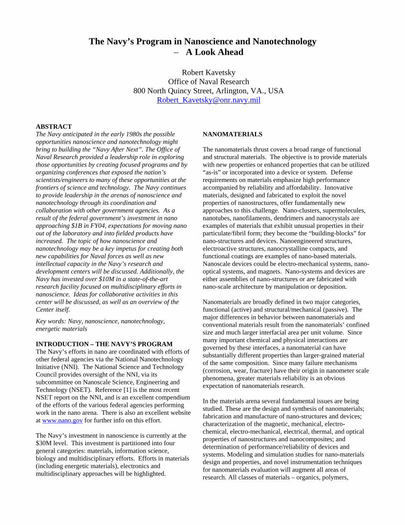
glasses, metals, alloys, non-traditional semiconductors, ceramics and composites fall in the nanomaterials category. It is envisioned the Navy will benefit in many applications areas that take advantage of the potentially superior properties of nanomaterials. Examples include fracture resistance in nanostructured coatings for greater lifetimes; scattering of multiple phonon frequencies providing enhanced thermal management materials and thermoelectric devices; reduced diffusion distances in electrodes and cell architectures enabling simultaneous increases in battery power and energy densities; high surface area particles for sensing and novel catalyst applications; and, enhanced electron transport in nanowire composites providing potential for controlled dielectric constants. One specific example of a class of nanomaterials currently in use is ceramic coatings. In the early 1990’s the science base for nanophase materials began to expand rapidly. In 1996 the first nanostructured coating was produced by a thermal spray process. In 1997 nanostructured ceramic coatings were produced by a plasma spray process, and in 1998 these coatings were produced with a liquid precursor, greatly reducing cost, thus making them an economically viable product. In 1999 the Navy began full-scale testing of these coatings on ship-board components, and in 2002 these coatings were used on submarine air intake/exhaust valves. The starting materials for fabricating the Al2O3-TiO2 coatings are ultra-fine particles of the two components (particle size about 30-50 nm). These particles cannot be sprayed directly, due to the ultra-fine morphology, but are agglomerated into composite aggregates about 30-100 microns in diameter by dispersing the particles in a fluid and spray drying. The agglomerates are then sprayed onto the surface to be coated using a plasma torch, which heats and accelerates the agglomerated particles. Figure 1 shows the spray being applied to a number of components being readied for testing. Figure 1. Plasma spray being applied to test samples. The key to the process is selecting the spray conditions such that only partial melting is achieved. The melted material undergoes rapid solidification forming a
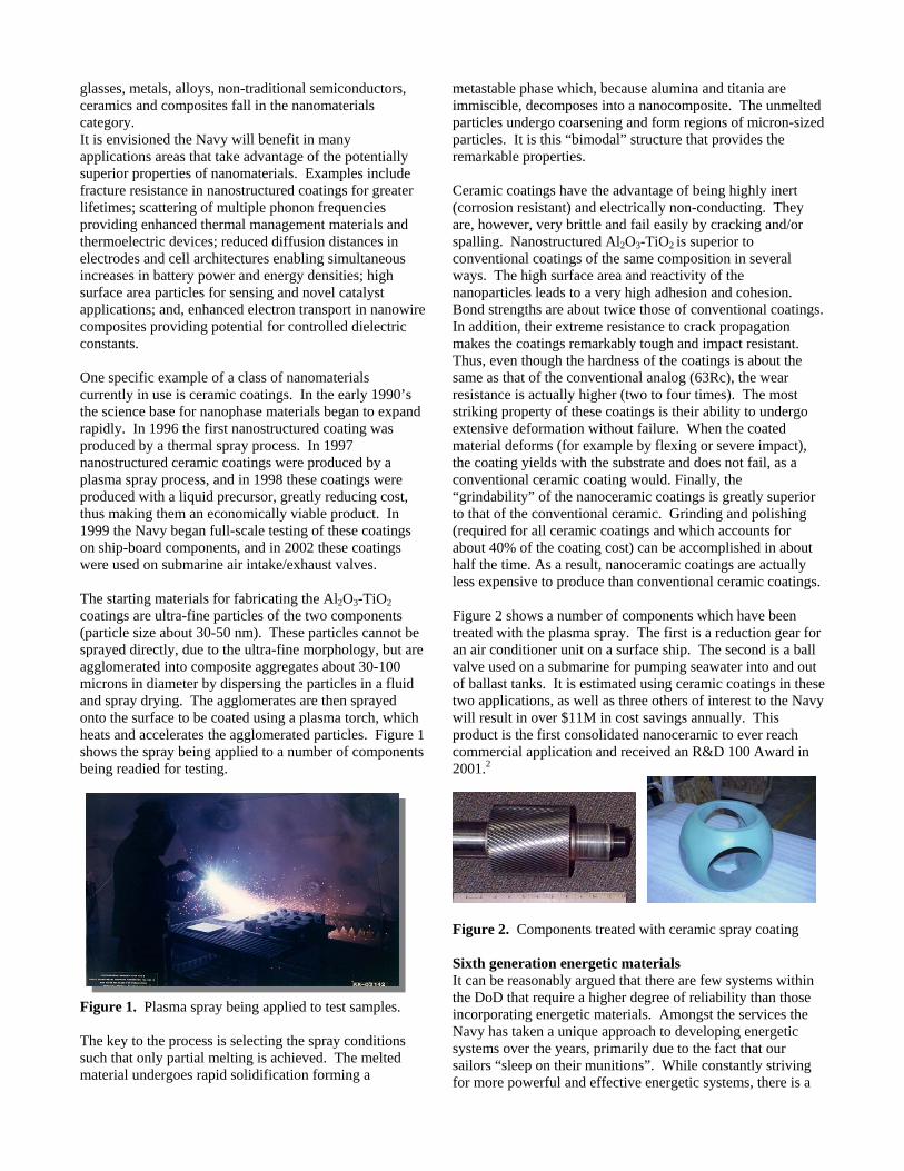
metastable phase which, because alumina and titania are immiscible, decomposes into a nanocomposite. The unmelted particles undergo coarsening and form regions of micron-sized particles. It is this “bimodal” structure that provides the remarkable properties. Ceramic coatings have the advantage of being highly inert (corrosion resistant) and electrically non-conducting. They are, however, very brittle and fail easily by cracking and/or spalling. Nanostructured Al2O3-TiO2 is superior to conventional coatings of the same composition in several ways. The high surface area and reactivity of the nanoparticles leads to a very high adhesion and cohesion. Bond strengths are about twice those of conventional coatings. In addition, their extreme resistance to crack propagation makes the coatings remarkably tough and impact resistant. Thus, even though the hardness of the coatings is about the same as that of the conventional analog (63Rc), the wear resistance is actually higher (two to four times). The most striking property of these coatings is their ability to undergo extensive deformation without failure. When the coated material deforms (for example by flexing or severe impact), the coating yields with the substrate and does not fail, as a conventional ceramic coating would. Finally, the “grindability” of the nanoceramic coatings is greatly superior to that of the conventional ceramic. Grinding and polishing (required for all ceramic coatings and which accounts for about 40% of the coating cost) can be accomplished in about half the time. As a result, nanoceramic coatings are actually less expensive to produce than conventional ceramic coatings. Figure 2 shows a number of components which have been treated with the plasma spray. The first is a reduction gear for an air conditioner unit on a surface ship. The second is a ball valve used on a submarine for pumping seawater into and out of ballast tanks. It is estimated using ceramic coatings in these two applications, as well as three others of interest to the Navy will result in over $11M in cost savings annually. This product is the first consolidated nanoceramic to ever reach commercial application and received an R&D 100 Award in 2001.2
Figure 2. Components treated with ceramic spray coating Sixth generation energetic materials It can be reasonably argued that there are few systems within the DoD that require a higher degree of reliability than those incorporating energetic materials. Amongst the services the Navy has taken a unique approach to developing energetic systems over the years, primarily due to the fact that our sailors “sleep on their munitions”. While constantly striving for more powerful and effective energetic systems, there is a
corresponding emphasis as well on making sure these systems are insensitive to unplanned stimuli and do not operate until desired. In addition to those seemingly contradictory requirements there has been of late greapressure to reduce the development time for new systemincluding those with energetic materials, to be deployed into the fleet.
t s,
he Navy has a long and distinguished history of
2 new
e
everal research initiatives are underway between the
re
ne approach to increasing performance is to place the
ditional
tion using
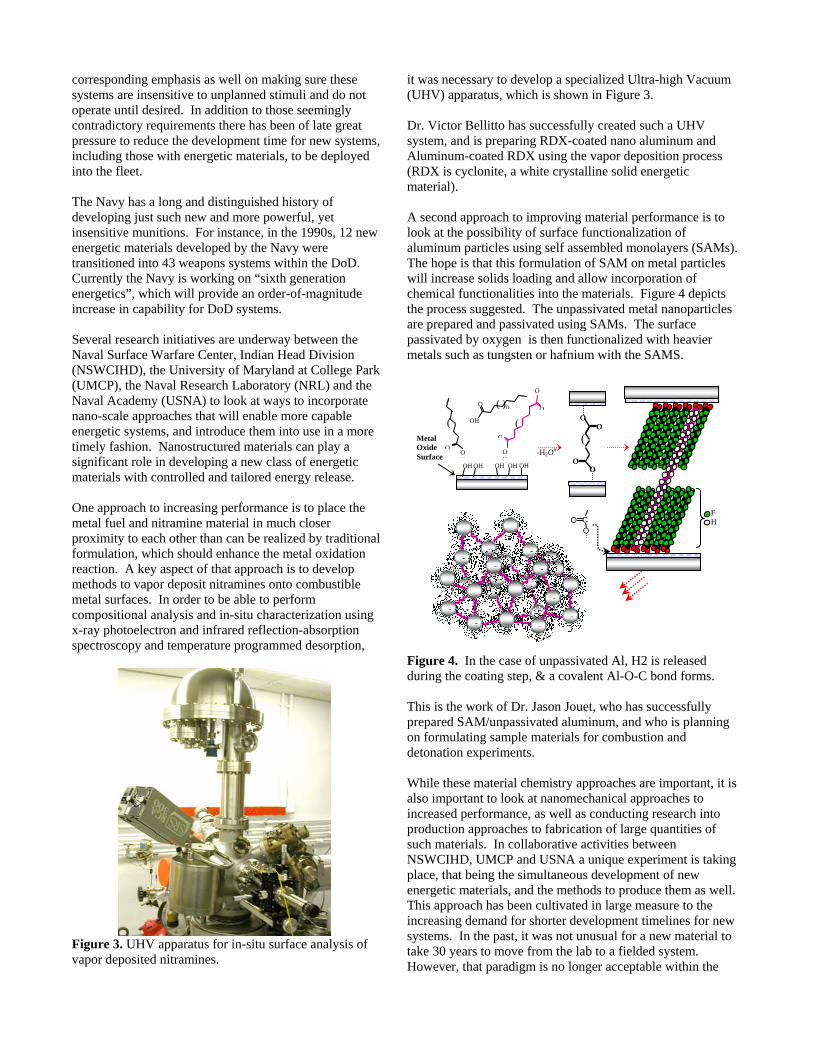
UHV apparatus for in-situ surface analysis of
sited nitramines.
h is shown in Figure 3.
a UHV stem, and is preparing RDX-coated nano aluminum and
ss
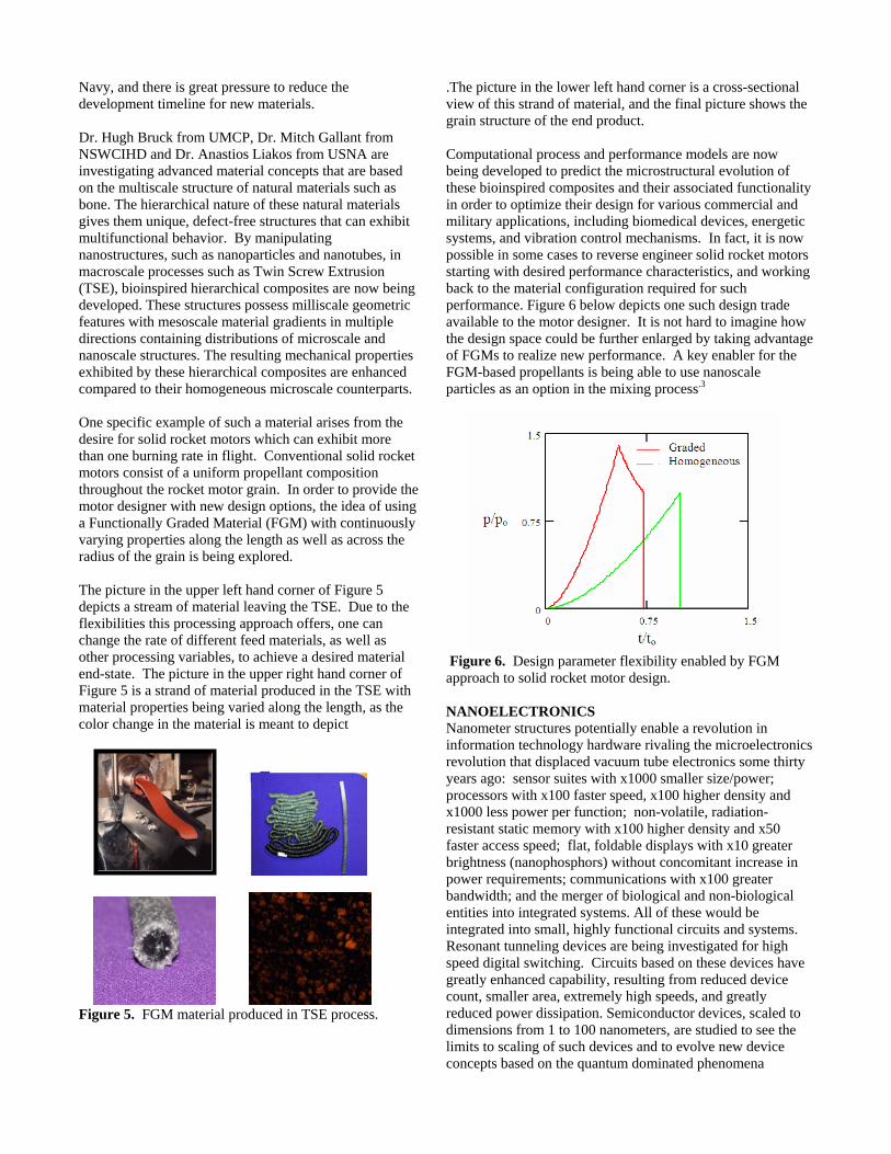
pproach to improving material performance is to ok at the possibility of surface functionalization of
. rticles
ticles
e case of pas ated Al, H2 is released during the coating step, & a covalent Al-O-C bond forms.
repared SAM/unpassivated aluminum, and who is planning
istry approaches are important, it is lso important to look at nanomechanical approaches to
f
ng ew
e
to
Tdeveloping just such new and more powerful, yet insensitive munitions. For instance, in the 1990s, 1energetic materials developed by the Navy were transitioned into 43 weapons systems within the DoD. Currently the Navy is working on “sixth generation energetics”, which will provide an order-of-magnitudincrease in capability for DoD systems. SNaval Surface Warfare Center, Indian Head Division (NSWCIHD), the University of Maryland at College Park(UMCP), the Naval Research Laboratory (NRL) and the Naval Academy (USNA) to look at ways to incorporate nano-scale approaches that will enable more capable energetic systems, and introduce them into use in a motimely fashion. Nanostructured materials can play a significant role in developing a new class of energeticmaterials with controlled and tailored energy release. Ometal fuel and nitramine material in much closer proximity to each other than can be realized by traformulation, which should enhance the metal oxidation reaction. A key aspect of that approach is to develop methods to vapor deposit nitramines onto combustiblemetal surfaces. In order to be able to perform compositional analysis and in-situ characterizax-ray photoelectron and infrared reflection-absorption spectroscopy and temperature programmed desorption,
Figure 3.vapor depo
it was necessary to develop a specialized Ultra-high Vacuum (UHV) apparatus, whic Dr. Victor Bellitto has successfully created suchsyAluminum-coated RDX using the vapor deposition proce(RDX is cyclonite, a white crystalline solid energetic material). A second aloaluminum particles using self assembled monolayers (SAMs)The hope is that this formulation of SAM on metal pawill increase solids loading and allow incorporation of chemical functionalities into the materials. Figure 4 depicts the process suggested. The unpassivated metal nanoparare prepared and passivated using SAMs. The surface passivated by oxygen is then functionalized with heavier metals such as tungsten or hafnium with the SAMS.
(
C O
O
O
Figure 4. In th un siv
This is the work of Dr. Jason Jouet, who has successfully pon formulating sample materials for combustion and detonation experiments. While these material chemaincreased performance, as well as conducting research into production approaches to fabrication of large quantities osuch materials. In collaborative activities between NSWCIHD, UMCP and USNA a unique experiment is takiplace, that being the simultaneous development of nenergetic materials, and the methods to produce them as well. This approach has been cultivated in large measure to thincreasing demand for shorter development timelines for new systems. In the past, it was not unusual for a new material take 30 years to move from the lab to a fielded system. However, that paradigm is no longer acceptable within the
O
O O
Metal Oxide Surface
OOH
O
OH
O
OH
O
OH
(
OH OH OOH OH
( )n
(
H
-H2O†
AM
M
M
MM
M
M
M
M
M
M
M
M
M M
M
M
AM
M
M
MM
M
MM
MM
FH
Navy, and there is great pressure to reduce the development timeline for new materials. Dr. Hugh Bruck from UMCP, Dr. Mitch Gallant from
SWCIHD and Dr. Anastios Liakos from USNA are
t
trusion g
tric
es ed
esire for solid rocket motors which can exhibit more t
ng
er of Figure 5 epicts a stream of material leaving the TSE. Due to the
al f
Figure 5. FGM material pro
Ninvestigating advanced material concepts that are basedon the multiscale structure of natural materials such asbone. The hierarchical nature of these natural materials gives them unique, defect-free structures that can exhibimultifunctional behavior. By manipulating nanostructures, such as nanoparticles and nanotubes, in macroscale processes such as Twin Screw Ex(TSE), bioinspired hierarchical composites are now beindeveloped. These structures possess milliscale geomefeatures with mesoscale material gradients in multiple directions containing distributions of microscale and nanoscale structures. The resulting mechanical propertiexhibited by these hierarchical composites are enhanccompared to their homogeneous microscale counterparts. One specific example of such a material arises from the dthan one burning rate in flight. Conventional solid rockemotors consist of a uniform propellant composition throughout the rocket motor grain. In order to provide the motor designer with new design options, the idea of usia Functionally Graded Material (FGM) with continuously varying properties along the length as well as across the radius of the grain is being explored. The picture in the upper left hand corndflexibilities this processing approach offers, one can change the rate of different feed materials, as well as other processing variables, to achieve a desired materiend-state. The picture in the upper right hand corner oFigure 5 is a strand of material produced in the TSE withmaterial properties being varied along the length, as the color change in the material is meant to depict
duced in TSE process.
.The picture in the lower left hand corner is a cross-sectional view of this strand of material, and the final picture shows the grain structure of the end product. Computational process and performance models are now being developed to predict the microstructural evolution of these bioinspired composites and their associated functionality in order to optimize their design for various commercial and military applications, including biomedical devices, energetic systems, and vibration control mechanisms. In fact, it is now possible in some cases to reverse engineer solid rocket motors starting with desired performance characteristics, and working back to the material configuration required for such performance. Figure 6 below depicts one such design trade available to the motor designer. It is not hard to imagine how the design space could be further enlarged by taking advantage of FGMs to realize new performance. A key enabler for the FGM-based propellants is being able to use nanoscale particles as an option in the mixing process.3
Figure 6. Design parameter flexibility enabled by FGM approach to solid rocket motor design. NANOELECTRONICS Nanometer structures potentially enable a revolution in information technology hardware rivaling the microelectronics revolution that displaced vacuum tube electronics some thirty years ago: sensor suites with x1000 smaller size/power; processors with x100 faster speed, x100 higher density and x1000 less power per function; non-volatile, radiation-resistant static memory with x100 higher density and x50 faster access speed; flat, foldable displays with x10 greater brightness (nanophosphors) without concomitant increase in power requirements; communications with x100 greater bandwidth; and the merger of biological and non-biological entities into integrated systems. All of these would be integrated into small, highly functional circuits and systems. Resonant tunneling devices are being investigated for high speed digital switching. Circuits based on these devices have greatly enhanced capability, resulting from reduced device count, smaller area, extremely high speeds, and greatly reduced power dissipation. Semiconductor devices, scaled to dimensions from 1 to 100 nanometers, are studied to see the limits to scaling of such devices and to evolve new device concepts based on the quantum dominated phenomena
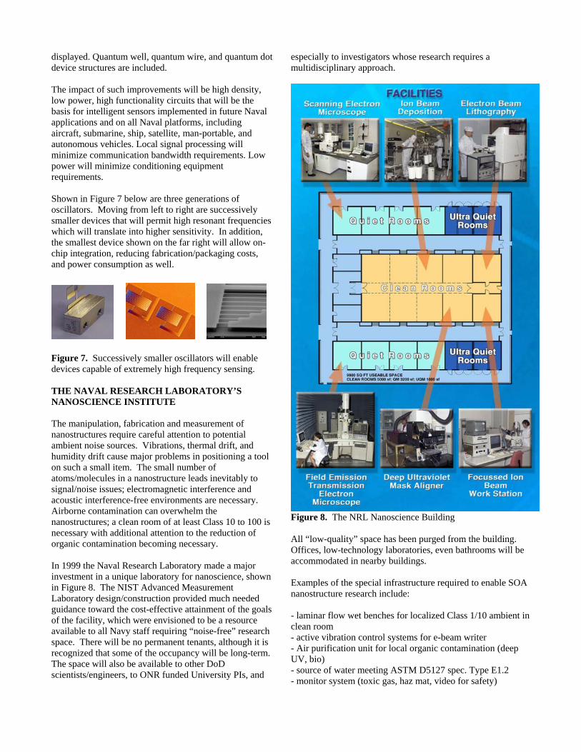
displayed. Quantum well, quantum wire, and quantum dot device structures are included. The impact of such improvements will be high density, low power, high functionality circuits that will be the basis for intelligent sensors implemented in future Naval applications and on all Naval platforms, including aircraft, submarine, ship, satellite, man-portable, and autonomous vehicles. Local signal processing will minimize communication bandwidth requirements. Low power will minimize conditioning equipment requirements. Shown in Figure 7 below are three generations of oscillators. Moving from left to right are successively smaller devices that will permit high resonant frequencies which will translate into higher sensitivity. In addition, the smallest device shown on the far right will allow on-chip integration, reducing fabrication/packaging costs, and power consumption as well.
Figure 7. Successively smaller oscillators will enable devices capable of extremely high frequency sensing. THE NAVAL RESEARCH LABORATORY’S NANOSCIENCE INSTITUTE The manipulation, fabrication and measurement of nanostructures require careful attention to potential ambient noise sources. Vibrations, thermal drift, and humidity drift cause major problems in positioning a tool on such a small item. The small number of atoms/molecules in a nanostructure leads inevitably to signal/noise issues; electromagnetic interference and acoustic interference-free environments are necessary. Airborne contamination can overwhelm the nanostructures; a clean room of at least Class 10 to 100 is necessary with additional attention to the reduction of organic contamination becoming necessary. In 1999 the Naval Research Laboratory made a major investment in a unique laboratory for nanoscience, shown in Figure 8. The NIST Advanced Measurement Laboratory design/construction provided much needed guidance toward the cost-effective attainment of the goals of the facility, which were envisioned to be a resource available to all Navy staff requiring “noise-free” research space. There will be no permanent tenants, although it is recognized that some of the occupancy will be long-term. The space will also be available to other DoD scientists/engineers, to ONR funded University PIs, and
especially to investigators whose research requires a multidisciplinary approach.
Figure 8. The NRL Nanoscience Building All “low-quality” space has been purged from the building. Offices, low-technology laboratories, even bathrooms will be accommodated in nearby buildings. Examples of the special infrastructure required to enable SOA nanostructure research include: - laminar flow wet benches for localized Class 1/10 ambient in clean room - active vibration control systems for e-beam writer - Air purification unit for local organic contamination (deep UV, bio) - source of water meeting ASTM D5127 spec. Type E1.2 - monitor system (toxic gas, haz mat, video for safety)
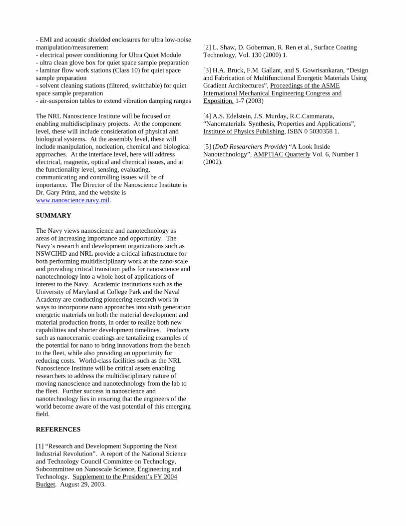
- EMI and acoustic shielded enclosures for ultra low-noise manipulation/measurement - electrical power conditioning for Ultra Quiet Module - ultra clean glove box for quiet space sample preparation - laminar flow work stations (Class 10) for quiet space sample preparation - solvent cleaning stations (filtered, switchable) for quiet space sample preparation - air-suspension tables to extend vibration damping ranges The NRL Nanoscience Institute will be focused on enabling multidisciplinary projects. At the component level, these will include consideration of physical and biological systems. At the assembly level, these will include manipulation, nucleation, chemical and biological approaches. At the interface level, here will address electrical, magnetic, optical and chemical issues, and at the functionality level, sensing, evaluating, communicating and controlling issues will be of importance. The Director of the Nanoscience Institute is Dr. Gary Prinz, and the website is www.nanoscience.navy.mil. SUMMARY The Navy views nanoscience and nanotechnology as areas of increasing importance and opportunity. The Navy’s research and development organizations such as NSWCIHD and NRL provide a critical infrastructure for both performing multidisciplinary work at the nano-scale and providing critical transition paths for nanoscience and nanotechnology into a whole host of applications of interest to the Navy. Academic institutions such as the University of Maryland at College Park and the Naval Academy are conducting pioneering research work in ways to incorporate nano approaches into sixth generation energetic materials on both the material development and material production fronts, in order to realize both new capabilities and shorter development timelines. Products such as nanoceramic coatings are tantalizing examples of the potential for nano to bring innovations from the bench to the fleet, while also providing an opportunity for reducing costs. World-class facilities such as the NRL Nanoscience Institute will be critical assets enabling researchers to address the multidisciplinary nature of moving nanoscience and nanotechnology from the lab to the fleet. Further success in nanoscience and nanotechnology lies in ensuring that the engineers of the world become aware of the vast potential of this emerging field. REFERENCES [1] “Research and Development Supporting the Next Industrial Revolution”. A report of the National Science and Technology Council Committee on Technology, Subcommittee on Nanoscale Science, Engineering and Technology. Supplement to the President’s FY 2004 Budget. August 29, 2003.
[2] L. Shaw, D. Goberman, R. Ren et al., Surface Coating Technology, Vol. 130 (2000) 1. [3] H.A. Bruck, F.M. Gallant, and S. Gowrisankaran, “Design and Fabrication of Multifunctional Energetic Materials Using Gradient Architectures”, Proceedings of the ASME International Mechanical Engineering Congress and Exposition, 1-7 (2003) [4] A.S. Edelstein, J.S. Murday, R.C.Cammarata, “Nanomaterials: Synthesis, Properties and Applications”, Institute of Physics Publishing, ISBN 0 5030358 1. [5] (DoD Researchers Provide) “A Look Inside Nanotechnology”, AMPTIAC Quarterly Vol. 6, Number 1 (2002).