the new standard by jim rowe components!
TRANSCRIPT

34 Everyday Practical Electronics, January 2018
IF YOU’VE been reading EPE for a while now, you’ll have noticed that
small electronic modules have been creeping into our projects.
These are not just Micromite, Ar-duino or Raspberry Pi boards, but really small and low-cost modules including real-time clocks/calendars (RTC), USB-to-UART serial ‘bridges’, UHF data transmitters and receivers, DDS signal generators, OLED/LCD panels, touch-screen TFT LCDs, tem-perature/humidity sensors, microSD card interfaces and many more. They seem to be breeding like rabbits!
Many of these modules have sprung into life initially as ‘peripherals’ for baby micros like the Arduino (ie, shields) and Raspberry Pi. But most of them have a lot of other applications in circuits and designs using standard TTL or CMOS ICs, and even in designs using olde-worlde discrete transistors.
But the really big advantage of this new generation of pre-built modules is that most of them are surprisingly low in cost. In fact, with many of them, you’ll find that the cost of a complete module is much less than the price you’d pay for the main IC chip used in them.
A prime example is the popular real-time clock/calendar module using Maxim’s very accurate DS3231 RTC chip — plus a 24C32 4KB EEPROM, in most cases. Although the module is usually ad-vertised as intended to be used with an Arduino, it has a standard I²C (‘Inter-IC’) in-
terface and can actually be used with most other micros (we used it with the Micromite in our Touchscreen Super Clock).
So that’s the rationale behind this series of articles on the new ‘el cheapo’ modules. They’re readily available, often have many applica-tions and they’re usually much cheap-er than building up the same circuits for yourself. As a result, they’ve now reached the status of being just stand-ard circuit components. The Electron-ic Modules As Components or ‘EMAC’ revolution has begun!
Let’s get the ball rolling by looking at real-time clock/calendar modules.
RTC modulesProbably the first low-cost RTC mod-ules to appear were those based on the Philips/NXP PCF8563 chip, a low-power 8-pin CMOS device which has an I²C interface but needs an external 32.768kHz crystal. Modules based on the PCF8563 are still available at low cost from eBay or AliExpress, but they tend to be less popular than
modules based on one of two newer Maxim chips: either the DS1307 or the DS3231.
Like the PCF8563, the DS1307 needs an external 32kHz crystal. How-ever, it also has a built-in power sense circuit which switches to a backup battery when it detects a power fail-ure. It has 56 bytes of internal non-volatile SRAM and a standard I²C interface, making it compatible with just about every type of microcon-troller module such as the Arduino or the Micromite.
It does have one shortcoming, though: the time-keeping accuracy is inclined to drift a little with tem-perature and so it can vary by a few minutes a month.
Clock/calendar modules using the DS1307 tend to cost more than those using the PCF8563, but they often include extras like a DS18B20 temperature sensor and a 24C32 se-rial EEPROM (32Kbits = 4KB). This makes them quite attractive for ap-plications where extreme accuracy isn’t too critical.
But modules based on the DS3231 chip are currently the most popular, partly because the DS3231 has an on-chip temperature-compensated crys-tal oscillator and crystal.
It also includes an internal temper-ature-compensated voltage reference and comparator, both to maintain its own supply voltage and to automati-cally switch to a backup supply when necessary.
These features allow it to provide significantly higher timekeeping ac-curacy: better than ±2ppm between 0
By JIM ROWEThe new standard components! Using Cheap Asian Electronic Modules Part 1
This is the first of a series of small articles which will help you take advantage of the wide range of handy pre-built electronic modules that are now available from Asia. This month, we review the DS3231 real-time clock (RTC), which is the per-fect partner for popular microcontrollers like the Arduino or Micromite.
chip
e as
cpct
aaocn
sTop view of the DS3231 module

Everyday Practical Electronics, January 2018 35
and 40°C, or ±2 minutes per year for a temperature range of –40°C to +85°C. Its single shortcoming compared with the DS1307 is that it lacks the internal non-volatile SRAM.
Despite the advantages offered by the DS3231, modules using it tend to cost no more than those based on the DS1307 or the PCF8563. And this ap-plies for modules like the one shown in the pictures, which also includes a 24C32 serial EEPROM.
As mentioned earlier, this is the RTC module that has been used in a number of recent projects like the Touchscreen Super Clock and the Micromite Explore 100, so it’s the one we’ll now concentrate on.
DS3231 RTCAs shown in the circuit diagram of Fig.1, there isn’t a great deal in this module apart from the DS3231 chip itself (IC1), its 3.6V backup battery and the 24C32 serial EEPROM (IC2). We’ll discuss the rest of the components and circuitry shortly after we’ve looked at what’s inside the DS3231.
Its compact 16-pin small outline (SO) SMD package contains an I²C data bus interface, address decoding for the 18 internal time, date and control registers, a temperature sensor and a power control circuit which can swing over to the backup battery when the supply voltage (VCC) fails. Its block diagram is shown in Fig.2.
Then there’s a complete tempera-ture-compensated 32.768kHz crystal oscillator (TCXO), followed by a fre-quency divider chain and all of the time (seconds/minutes/hours), date (day of week, day of month, month and year), alarm, status and control reg-isters. Finally, there’s reset circuitry plus output buffers for both the 32kHz TCXO oscillator and the square wave output when it’s enabled.
Note that since the module tracks the date as well as the time, it is more correctly described as a real-time clock and calendar (RTCC) module but we’ll stick with the more com-mon RTC term.
As well as the time and date reg-isters, the DS3231 also provides two time-of-day alarm functions which are programmable via two sets of dedi-cated registers. These can generate an interrupt output signal via pin 3 (INT/SQW), for feeding directly back to a micro.
When pin 3 is not being used to provide this alarm interrupt function, it can be used to provide square wave timing signals derived from the 32kHz TCXO. The square waves can be pro-grammed for one of four frequencies: 1Hz, 1.024kHz, 4.096kHz or 8.192kHz.
These are in addition to the 32.768kHz signal made available at pin 1.
All of the DS3231’s function set-tings, along with the initial time and date, can be programmed using the I²C bus to write into the appropriate inter-nal registers. Then the time, date and status can be subsequently obtained by using the I²C bus to read from the same registers.
Pins 15 and 16 of the device are used for the I²C bus connections: pin 15 for the SDA serial data line and pin 16 for the SCL serial clock line. On the module shown, these are both pro-vided with surface-mount 4.7k� pull-up resistors to VCC, as are pin 1, the 32.768kHz output and pin 3, the INT/squarewave output. (The latter two pins are open-drain outputs, so they need the external pull-up resistors.)
That’s probably about all you need to know about the DS3231 itself, apart from the way that pin 14 (VBAT) is used for the connection to the 3.6V lithium-ion rechargeable backup battery. In the module shown here, diode D1 and its series 200� resistor are used to main-tain the battery charge when VCC is
connected to the module. LED1 and its series 1k� resistor are used to pro-vide a power-on indicator. We’ll have more to say about battery options later.
Note the two I/O headers, labelled in Fig.1 as CON1 and CON2. CON1 provides pins for both the 32kHz and SQW/INT outputs, as well as the SCL/SDA/VCC/GND bus connections, while CON2 provides only the latter four connections, essentially to allow daisy-chaining further devices to the I²C bus – additional memory chips, for example.
Now let’s look at IC2, the 24C32 serial EEPROM chip, which is some-thing of a bonus. The 24C32 is a 4KB (32Kb) device, with a standard I²C serial interface. In this module, the SDA line (pin 5) and SCL line (pin 6) are connected in parallel with those for IC1, to the module’s SDA and SCL lines at both CON1 and CON2.
To allow IC2 to be addressed by the micro without conflicting with commands or data sent to or received from IC1, it has a different slave address on the I²C bus. In fact, it can have any of eight different slave
VBAT
Vcc
NC GND
SCL
SDA
RST
INT SQW/
32kHz1
2
3
4
5–12 13
14
15
16
IC13231DSIC13231DS
AA
KK
32k
SQW
SCL
SCL
SDA
SDA
VCC
VCC
GND
GND
4x4.7k
4x4.7k
100nF 10 F 1k200
LED1D1
1N4148
3.6V-LI ION
BATTERY( )RECHARGEABLE
SDA
SCL
Vss
Vdd
A0
A1
A2
NC
IC224C 23
IC224C 23
1
2
3
4
5
6
78
A0 A2A1
CON1
CON2
(TO SET SLAVE2)ADDRESS OF IC
I C ( ) 24C32SLAVE ADDRESSES HEX FOR EEPROM
MSD FIXED( ) A2 A1 A0 WRITE READ
A
A
A
A
A
A
A
A
1
1
1
1
0
0
0
0
1
1
0
0
1
1
0
0
1
0
1
0
1
0
1
0
2
AE
AC
AA
A8
A6
A4
A2
A0
AF
AD
AB
A9
A7
A5
A3
A1
DEFAULT ADDRESS(NO LINKS ON PADS
A0, A1 A2)FOR OR
NOTE SLAVE: I C3231ADDRESS FOR DS IS
D0 ( ) ,HEX FOR WRITINGD1 ( )HEX FOR READING
2
1 0 1 0 A2 A1 A0R
W
24C32 ADDRESS BYTE FORMAT
FIXED SET BYLINKS
Fig.1: complete circuit for the DS3231-based RTC module. Both CON1 and CON2 provide serial bus and power connections, allowing extra devices to be connected. Note that the I2C bus should have only one set of pull-up resistors.

36 Everyday Practical Electronics, January 2018
addresses, as set by the voltage levels of pins 1, 2 and 3 (labelled A0, A1 and A2).
As shown in Fig.1, the module pulls all three pins up to VCC via the 4.7k� resistors by default, which gives IC2 a slave address of AE/AF hex (AEh for writing, AFh for reading). But it also provides three pairs of pads on the PCB so that any of the three address pins can be pulled low (to ground) by soldering across the A0, A1 or A2 pads. This allows the slave address of IC2 to be set to any of the eight possible values, as shown.
So since the slave address of IC1 (the DS3231) is fixed at D0/1 hex (D0 for writing, D1 for reading), there is no conflict. In fact, the main reason for changing the slave address of IC2 via the wire links would be to avoid a conflict with any other devices that may be attached to the I²C bus.
How it’s usedSince both the DS3231 and 24C32 devices on the module are intended for
use via the I²C bus, this makes it easy to use with any micro or other system provided with at least one I²C inter-face. (Even if you don’t have such an interface, you can use two GPIO pins in ‘bit banging’ mode, but that’s out-side the scope of this article.)
For example, to use it with an Ar-duino Uno or similar all you need to do is connect the SCL line on the module to the AD5/SCL pin on the Ar-duino, the SDA line to the AD4/SDA pin, the VCC pin to the +5V pin and the GND pin to one of the Arduino’s GND pins.
It’s just as easy with the Micromite. In this case, the SCL pin connects to pin 17 on the Micromite’s main I/O pin strip, while the SDA pin connects to pin 18 next to it. Then the VCC and GND pins connect to the +5V pin and GND pins on the same pin strip.
Programming either of the chips on the module should also be fairly straightforward, because of the I2C interfacing. The main thing to re-
member is that I2C transactions always begin with a control byte sent by the master (the mi-crocontroller), specifying the address of the slave device it wishes to communicate with and whether it wants to write to or read from the device.
So, for example, the con-trol byte to initiate a write
operation to one of the registers in the DS3231 would be D0h, while the control byte to read from one of the addresses in the 24C32 would be AFh (assuming it’s at the default address on your module).
After the slave device sends back an ‘ACK’ or acknowledge indication (to show that it’s present and ready for a transaction), the micro then sends the address of the register or memory location in the device that it wants to write data to or read it from. When this has been acknowledged, the actual write or read transactions can take place.
If this sounds a bit complicated, you’ll be relieved to hear that if you’re using one of the popular micros like the Arduino or Micromite, you prob-ably don’t need to worry about this yourself. That’s because this has usu-ally been taken care of in small code libraries, with functions specifically written for I²C data communications. In the case of the Micromite, in fact, I²C communication is handled by the MMBASIC interpreter.
For example, if you are using an Arduino, the Arduino IDE application already includes a ‘Wire’ library, pro-viding about nine different functions for passing data between the micro and an I²C device.
Similarly, if you’re using a Micro-mite, you’ll find that Geoff Graham’s MMBASIC already includes functions like RTC SETTIME, RTC GETTIME, RTC SETREG and RTC GETREG spe-cifically for talking to the DS1307 or DS3231 RTC devices. And there are other functions like I2C OPEN, I2C WRITE, I2C READ and I2C CLOSE for data transactions with other I2C devices (like the 24C32 EEPROM chip in the current module).
Finally, there’s also an automatic variable called MM.I2C, which can be read after any I2C transaction to find out the result status.
So all in all, the RTC module shown with its DS3231 clock/calendar chip (and bonus 24C32 EEPROM chip) is relatively easy to use, and exceptional value for money.
Here is a link to a useful web tutorial by John Boxall of tronixlabs, explain-ing how to use either the DS1307 or DS3231 RTC modules with an Ardui-no: http://bit.ly/2yTbIWy
Final note: this module has onboard pull-up resistors for the I²C bus, you may need to remove them, or avoid fit-ting pull-up resistors on the master, for it to share a bus with other peripherals.
CLOCK AND CALENDARREGISTERS
USER BUFFER(7 BYTES)
VOLTAGE REFERENCE;DEBOUNCE CIRCUIT;PUSHBUTTON RESET
I C INTERFACE AND2
ADDRESS REGISTERDECODE
POWER CONTROL
VVGND
CC
BAT
SCL
SDA
TEMPERATURESENSOR
CONTROL LOGIC/DIVIDER
ALARM, STATUS, ANDCONTROL REGISTERS
OSCILLATOR ANDCAPACITOR ARRAYX1
X2
N
32kHz
N
INT SQW/
SQUARE-WAVE BUFFER;INT/SQW CONTROL
N
RST
VCC
DS3231
1Hz
1Hz
Fig.2: block diagram for the DS3231. A comparator monitors both VCC and VBAT and the DS3231 is powered from whichever is higher. The oscillator is automatically temperature-compensated for accuracy.
Rear view of the DS3231 module showing the 3.6V Li-ion backup battery (pin 14) which
powers the real time clock when the supply voltage (VCC) fails.
devices on the module are intended for
memalwbycradwat
Rear view ofthe 3.6V Li-ion b
Reproduced by arrangement with SILICON CHIP
magazine 2017.www.siliconchip.com.au

1 www.handsontec.com
Handson Technology
Data Specs
DS3231 High Precision Real Time Clock
DS3231 is a low cost and extremely accurate I2C real-time clock, with an integrated crystal
and temperature-compensated crystal oscillator (TCXO). DS3231 can be operated using
supply voltages ranging from 2.3V to 5.5V and it also features battery backup capabilities.
The on-board AT24C32 32KB EEPROM that can be used to add non-volatile data storage to
your electronic projects and prototypes.
SKU: MDU-1036
Brief Data:
Standard 2.54mm pins pitch for input and output connections.
Two programmable square-wave outputs.
Backup battery socket compatible with CR2032 3V Lithium batteries.
Clock accuracy: ±2ppm.
32KB EEPROM Memory chip: AT24C32.
On-chip temperature sensor with an accuracy of ±3℃.
I2C bus interface maximum speed: 400kHz.
Small Size: 38 x 22 x 14 mm.
28 Everyday Practical Electronics, March 2018
IF THE HC-SR04 module shown in the picture looks familiar, that’s be-
cause it has already been used in Geoff Graham’s Ultrasonic Garage Parking Assistant, published in the June 2017 is-sue. But this module doesn’t have to be used with a microprocessor module like a Micromite or an Arduino, it can also be used with much simpler circuitry.
Before we get to how it works, we should note that these ultrasonic sen-sor modules have been around for about six years, beginning life as an add-on ‘shield’ for the Arduino. Since then, they have gone through a num-ber of iterations, all bearing the same HC-SR04 label but with various minor circuit and component changes. We suspect this has been due to various manufacturers working out ways of
reducing costs, rather than seeking to achieve better performance.
The bottom line is that although some of these slightly different HC-SR04 modules are still being sold, they all seem to function and perform much the same. So don’t worry if the module you buy looks a little different from that shown in the photos. The odds are that if your module carries the label HC-SR04, it will work just like any other HC-SR04.
Current HC-SR04 modules are based on a PCB measuring 45 × 20mm. On the top side of the PCB is a pair of small (16mm diameter) ultrasonic transduc-ers with a 4MHz crystal between them.
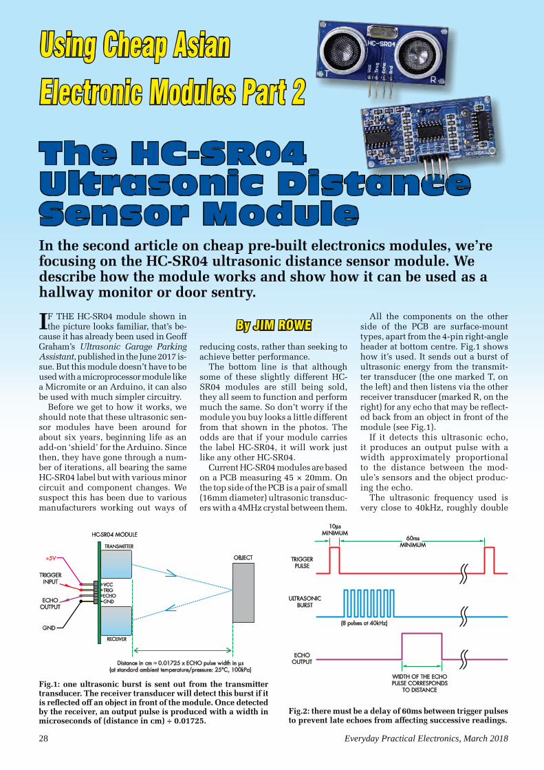
All the components on the other side of the PCB are surface-mount types, apart from the 4-pin right-angle header at bottom centre. Fig.1 shows how it’s used. It sends out a burst of ultrasonic energy from the transmit-ter transducer (the one marked T, on the left) and then listens via the other receiver transducer (marked R, on the right) for any echo that may be reflect-ed back from an object in front of the module (see Fig.1).
If it detects this ultrasonic echo, it produces an output pulse with a width approximately proportional to the distance between the mod-ule’s sensors and the object produc-ing the echo.
The ultrasonic frequency used is very close to 40kHz, roughly double
By JIM ROWE
The HC-SR04 Ultrasonic Distance Sensor ModuleIn the second article on cheap pre-built electronics modules, we’re focusing on the HC-SR04 ultrasonic distance sensor module. We describe how the module works and show how it can be used as a hallway monitor or door sentry.
≈
Fig.1: one ultrasonic burst is sent out from the transmitter transducer. The receiver transducer will detect this burst if it is reflected off an object in front of the module. Once detected by the receiver, an output pulse is produced with a width in microseconds of (distance in cm) ÷ 0.01725.
Fig.2: there must be a delay of 60ms between trigger pulses to prevent late echoes from affecting successive readings.
Using Cheap Asian Electronic Modules Part 2

Everyday Practical Electronics, March 2018 29
the highest frequency that can be heard by human ears. The burst of transmit-ted energy consists of eight pulses at 40kHz, so the transmitted burst lasts for only 200μs, as shown in Fig.2.
Since the speed of sound in air at 25°C and 100kPa (ie, 1 bar) is close to 345m/s (= 0.0345cm/μs) and the dis-tance travelled by the ultrasonic burst energy corresponds to double the dis-tance between the transducers and the reflecting object, we can calculate the distance from the delay as follows:
distance in cm =
0.0345 x echo pulse width (μs) 2= 0.01725 x echo pulse width (μs)
As shown in Fig.2, each measurement cycle begins when a positive trigger pulse of at least 10μs duration is ap-plied to the HC-SR04 module’s trigger input pin. When the echo has been detected, it then produces a pulse at the echo output pin. Note that there should be at least 60ms between trig-ger pulses, to prevent late echoes from one cycle causing false readings on the next. So in practice, it’s a good idea to limit the trigger pulse frequency to no more than 16Hz.
Circuit detailsThe full circuit for the HC-SR04 mod-ule is shown in Fig.3. It is based on an EM78P153S microcontroller (IC1), a low-power 8-bit CMOS device made by Elan Microelectronics in Hsinchu, Taiwan. This device has a 1024 × 13 bits one-time programmable (OTP) ROM plus 32 bytes of on-chip SRAM, and comes in a 14-pin SOIC package. It runs here with a 4MHz crystal be-tween pins 5 and 6.
When a TRIG pulse arrives at pin 1 of IC1 (from pin 3 of CON1), the con-troller generates a 40kHz burst signal of eight pulses at pins 13 and 14, with one pin 180° out of phase with the other. These go to pins 10 and 11 of IC3, a bus driver IC very similar to the MAX232. The outputs from IC3 (pins 7 and 14) connect across the transmit-ter transducer, effectively driving it in bridge mode to emit the bursts of ultrasonic energy.
Echoes picked up by the receive transducer pass through the four sec-tions of IC2, an LM324 quad op amp. These provide amplification, band-pass filtering and phase detection, with the result that a received echo pulse is fed back to pin 10 of IC1. The micro then compares the timing of the leading edge of this received
echo pulse with the leading edge of the transmitted burst fed to IC3 and the transmit transducer, and produces an echo output pulse at pin 2 with its width equal to the time difference. This echo output pulse appears at pin 2 of CON1.
How it’s usedIf you want to use the HC-SR04 mod-ule to actually measure the distance to an object or wall in front of it, the best way to do it is to hook it up to a microprocessor module like an Ar-duino, Micromite or Raspberry Pi. The micro’s program generates the trigger pulse to the HC-SR04, then measures the length of the echo pulse and cal-culates the corresponding distance.
There’s no need to worry about writing a program to do these tasks for you, because many people have already produced programs to do this. A quick search on the Arduino website (www.arduino.cc) or by using Google will find a sample program for the micro you’re using in short order.
If you want to use the HC-SR04 with a Micromite, Geoff Graham has already built a DISTANCE function into his MMBasic programming language for the Micromite family to make it re-ally easy.
�
�
�
�
�
�
� �
�
�
�
�
�
�
�
�
�
Fig.3: complete circuit diagram for the HC-SR04 ultrasonic sensor module. When IC1 detects a TRIG pulse at pin 1, a 40kHz burst signal of eight pulses is generated at pins 13 and 14 of IC1. This is taken to pins 10 and 11 of IC3 respectively, and output at pins 7 and 14 connecting to the transmit transducer.

Everyday Practical Electronics, March 2018
All you have to do to get the Micro-mite to trigger the HC-SR04 and then calculate the object distance from the echo pulse is use this one-line func-tion call:
d = DISTANCE(trig, echo)
Where ‘d’ is the distance in centime-tres, ‘trig’ is the Micromite’s I/O pin connected to the HC-SR04’s trigger input pin and ‘echo’ is the I/O pin connected to the HC-SR04’s echo out-put pin.
The only extra step is to connect the HC-SR04’s +5V and GND pins to the corresponding pins of your Micromite.
If you want to display the result ‘d’ on an alphanumeric LCD, you can do this using commands like:
LCD INIT ...LCD 1, 2, “Distance = “LCD 2, 6, STR$(d)and so on.
You can get a good idea of what’s in-volved in using the HC-SR04 with a Micromite from Geoff Graham’s arti-cle describing the Ultrasonic Garage Parking Assistant.
But say you want to use this mod-ule without a microcontroller at all. That’s fairly straightforward, as we’ll now demonstrate.
A simple intruder alarmFor example, to use it as an ultrason-ic intruder alarm, have a look at the circuit shown in Fig.4. It uses three low-cost CMOS ICs, a 2N7000 MOS-FET, three diodes, one LED, a piezo buzzer and some passive components.
This circuit and the HC-SR04 operate from a common 5V DC power supply, which can be from a USB plugpack or USB power bank.
IC1 is a hex Schmitt trigger invert-er package and we’re using just two sections of it, IC1a and IC1b. IC1a at upper left is connected as a relaxa-tion oscillator, to generate a stream of 60μs-wide pulses at a frequency of about 12Hz, ie, with a pulse spacing of about 83ms. These form the trigger pulses, which are fed to the HC-SR04 via pin 3 of CON1.
The rest of the circuit monitors the width of the echo pulses sent back from the HC-SR04 via pin 2 of CON1. If this varies significantly (indicating that something has moved between the sen-sor and the nearest object, like the op-posite wall of your entry hall), it sounds the alarm by switching on LED1 and the piezo buzzer connected across it.
This section is a little more com-plex. First, the incoming echo pulse passes through inverter IC1d, so that its leading edge is negative-going. The 1nF capacitor and 100k� resistor then form a differentiator circuit, which de-velops a narrow negative-going pulse from the negative-going leading edge of the inverted pulse.
This is then used to trigger IC2, a 7555 CMOS timer chip connected as a one-shot multivibrator. When IC2 is triggered, its output pin 3 switches high for a short time, determined by the 2.2μF capacitor connected from pins 6 and 7 to ground and the resist-ance connected between the same two pins and the +5V line.
As shown, this resistance is the series combination of a 10k� resistor
and VR1, a 100k� pot. So by varying VR1, we can vary the width of the pulse generated each time the one-shot is triggered.
The output of IC2 is connected to pin 2 of IC3a, one section of a 4070B quad XOR (exclusive-OR) gate. The echo pulses from the HC-SR04 are fed to pin 1 of IC3, the second input of the same XOR gate. Since the output of an XOR gate is high only when one of its inputs is high and the other low, it forms a pulse-width comparator.
Consider the situation where the HC-SR04 sensor is facing a wall, say 1.5m or 150cm away. The echo pulses fed back from the sensor will be very close to 8.7ms wide and these are fed to input pin 1 of IC3a.
If we adjust VR1 so that IC2 also produces 8.7ms-wide pulses, then since they start at virtually the same instant at the start of the echo pulse, both inputs of XOR gate IC3a will rise and fall at the same time. As a result, the output of IC3a (pin 3) will remain low at all times.
Fig.4: complete circuit for an ultrasonic intruder alarm using an HC-SR04 module. IC1a generates 60μs-wide trigger pulses at 12Hz, which are fed to pin 3 of CON1. The echo pulses trigger monostable multivibrator IC2, and IC3a then compares the width of the resulting pulse to the echo pulse. If these differ, LED1 lights and the piezo buzzer sounds.
This tiny active piezo transducer module from Jaycar can be used in the intruder alarm instead of the piezo buzzer.

Everyday Practical Electronics, March 2018
But if someone moves in front of the HC-SR04, this will cause the echo pulses to shorten, because the ultra-sonic energy reflected back by the person or object will be travelling over a smaller distance. So the echo pulse width will drop briefly to say 5-6ms, and as a result the inputs of IC3a will no longer be synchronised.
Although the pulses fed to pin 2 will still be high for 8.7ms, the echo pulses being fed to pin 1 will drop low after 5-6ms, so the output of IC3a will switch high for the remaining 2.7-3.7ms. These positive-going pulses will very quickly charge up the 1μF capacitor in the gate circuit of MOSFET Q1, via diode D3 and the 10k� series resistor, and this will turn on Q1, causing LED1 to light and the piezo buzzer to sound the alarm.
Then, when the intruding person or object moves away again and the echo pulses return to their original width of 8.7ms, the pulses fed to the two inputs of IC3a will be again be synchronised. There will be no more output pulses from IC3a and the 1μF capacitor will be discharged by the 1M� resistor connected across it. So within a couple of seconds, the buzzer and LED will switch off.
The circuit is quite easy to set up, too. All you need to do is wire it up and connect it to the HC-SR04 module using a suitable length of 4-conductor cable. Then mount the sensor module on one side of the hall or doorway you want to monitor, facing either a wall or a large fixed object such as a dresser, a chest of drawers or a filing cabinet.
Next, set pot VR1 to its fully anti-clockwise (ie, minimum resistance) position and turn on the 5V power supply. You’ll find that LED1 will immediately light, and if you have a piezo buzzer connected as well, it will sound. That’s because the pulses being generated by the one-shot IC2 will be shorter than the echo pulses coming from the HC-SR04.
Now slowly turn pot VR1 clockwise until LED1 turns off and the piezo buzzer goes silent. Your intruder alarm will then be set up and ready to detect the presence of a ‘foreign body’ in the space between the sen-sor and its reflecting wall. So we’ve done all this without a microproces-sor – apart from the EM78P153S micro inside the HC-SR04 sensor module itself, of course.
1 HC R0 ult asonic senso1 acti e pie o t ansduce module OR1 pie o u e1 100 � t impot ( R1)
Semiconductors1 1 819 diode ( 1)2 1 1 8 diodes ( 2)1 E an colou ( E 1)1 2 000 M E ( 1)1 010 o HC1 CM C ( C1)1 M CM time C ( C2)1 0 0 uad R ate C ( C3)
Capacitors (16V)1 2.21 12 100n1 1n
Resistors (0.25W, 5%)1 2.2M� 1 1M� 1 100 �2 10 � 1 1. � 1 0�1 100�
Parts List
Reproduced by arrangement with SILICON CHIP
magazine 2018.www.siliconchip.com.au
e t oni 30 2 /Ce t oni 3032e t oni 3012e t oni 2 30Ae t oni 2a nell AP 0/ 0a nell H 0/ 0a nell A3 /2a nell 1
Racal 1991Racal 2101Racal 9300Racal 9300
lu e 9lu e 99i at onics 100ea a d o aola t on 1 0/Polat on 12 3asa a o M03 2hu l P 320 Mhu l 210
HP33120AHP 3131AHP 3131A
scilloscope 00MH 2. /scilloscope 300MH 2. /scilloscope 2 Channel 100MH 1.2 /scilloscope ual ace 1 0MH 100M /scilloscope Channel 00MH
P 0 0 0 0A 1 itch ModeP 0 0 0 0AP 0 3 0 2A ice i ital
ine/s scillato 10H 1MHCounte / ime 1 0MH 9 i itCounte 20 H E
ue RM Milli oltmete H 20MH etcAs 9300
copemete 2 Channel 0MH 2 M /copemete 2 Channel 100MH /nthesised i nal ene ato 10MH 20 H
PA este 1/2 i it MM ue RM EEEain Phase Anal se 1mH 20 H
P 0 3 0 2A 2 Mete sP 0 30 0 2A ice
unction ene ato 0.002 2MH etc en ood ad edunction ene ato 100 mic oH 1 MH ni e sal Counte 3 H o ed unusedni e sal Counte 22 MH
1 0099
03 000
1900
1 029
121 9 09
/00
301 0 200
2 0 30000
3 0
STEWART OF READING1 A in t eet Mo time nea Readin R 3R
elephone: 0118 933 1111 a : 0118 9331275E E EC R C E E PME
Chec e site www.stewart-of-reading.co.uk(ALL PRICES PLUS CARRIAGE & VAT)
Please check availability before ordering or calling in
AM A E EAM A E E
R 202Ma coni 29R AP 2HP332 AHP3 1AHP 032AHP 22AHP 2 AHP 32HP AHP AHP83 1AHP83 31AHP8 8 AHP8 0AHP8 0EHP8 3AHP8HP8 2AMa coni 2022EMa coni 202Ma coni 2030Ma coni 230Ma coni 2 0Ma coni 29 /A/Ma coni 29Ma coni 29 AMa coni 200Ma coni 200AMa coni 200Ma coni 9 0 ith
P E 100 1 100 1 A o ed As eP E 0 30 0 30A
i nal ene ato 9 H 2. 1 H pt 0 /11Radio Communications est et
n unction ene ato 1H 2 0 Hnthesised unction ene atonamic i nal Anal se
P 0 0 0 0A 1000P 0 20 A ice o 0 0 2A iceP utputs P 0 20 0 AP 0 0 3. AP 0 0 0 9A
nthesised eep ene ato 10MH 20 Hnthesised i nal ene ato 1 20 H
Po e enso 0.01 18 H 3n 10upect um Anal se nthesised 0H 2.9 Hpect um Anal se nthesised 30H 2.9 Hpect um Anal se nthesised 9 H 22 Hpect um Anals e 100H 22 H
R ene ato 10 H 1280MHnthesised AM/ M i nal ene ato 10 H 1.01 Hnthesised i nal ene ato 9 H 2. Hnthesised i nal ene ato 10 H 1.3 H
Modulation MeteCounte 20 HCommunications est et a ious ptionsRadio Communications est etRadio Communications est etMic o a e est etMic o a e est et 10MH 20 HMic o a e est et 910 Po e Mete
3232
9008001919
00
3 03 0190000
2 0001 800
1 2 01 02 2 01 200
032800
02 0293 092
1 001 9 02 30029
2 000 –
FANTASTIC MODERN POWER SUPPLY ONLY IU HIGH PROGRAMMABLE
CA E PP E H P A RA CA E
PR PER 200MH A A E C PE 2 0
R A AR MM 32 R 2 H HA E
A MPER
E A HP 100MH C PE R R C MP E E H A
ACCE R E 12
800

1 www.handsontec.com
Handson Technology
User Guide
HC-SR04 Ultrasonic Sensor Module
HC-SR04 Ultrasonic Sensor is a very affordable proximity/distance sensor that has been
used mainly for object avoidance in various robotics projects. It has also been used in turret
applications, water level sensing, and even as a parking sensor.
SKU: SSR-1012
Brief Data:
Power Supply: 3.3~5 VDC
Quiescent Current : <2mA
Working Current: 2.8mA @ 5V
Effective Angle: <15°
Ranging Distance : 2cm – 400 cm or 1″ – 13ft
Connector: 4-pins header with 2.54mm pitch.
Dimension: 45mm x 20mm x 15mm
Weight 8.5-g.
2 Everyday Practical Electronics, March 2018
THE SECOND MODULE we’re looking at this month has been used in a
number of recent projects. It’s a serial USB-UART (universal asynchronous receiver/transmitter) bridge which al-lows just about any microcomputer or peripheral module to exchange data with a PC, via a standard USB port.
Let’s start by explaining what is meant by the rather clumsy term’serial USB-UART bridge’. First, a UART is an interface which can operate in one of several different common serial protocols. The serial protocol we’re most interested in (and which is most widely used) is 3.3V ‘TTL’ RS-232. The term ‘bridge’ simply refers to the fact that this module allows data to pass between the USB interface and UART interface unchanged.
In fact, we’ve already described a device with essentially the same purpose, the Microchip MCP2200 ‘protocol converter’ used in the USB/RS-232C Serial Interface which was published in the April 2015 issue.
Note that for a UART to provide a fully compatible RS-232 serial port, as used in many now-obsolete PCs, it’s necessary to provide level shifting from the UART’s 3.3V (TTL) signal-ling levels to the RS-232 bipolar logic levels of ±3-15V.
But these days, RS-232 is commonly used for short-range communications between microcontrollers and bridges and in this case, the TTL signal levels are all you really need.
The first serial USB-UART bridge modules to become popular were based
around British firm FTDI’s improved FT232R converter chips. However, these chips became so popular that some Asian firms made ‘clones’ of them, even going so far as copying the package markings.
Understandably, this upset FTDI and as a result they released a new version of their Windows VCP driver which was able to identify when a clone chip was being used and dis-able it. This ‘clone killer’ driver was included in an automatic update that Microsoft unwittingly provided to Windows users.
As a result, thousands of people found that their low-cost USB-UART converter modules, some inside com-mercial products, suddenly stopped working and became worthless. Natu-rally, this made many people cautious of buying any converter based on the FTDI FT232R chip, because of the diffi-culty in ensuring that you are buying a genuine FTDI chip rather than a clone chip that would stop working as soon as you tried to use it with Windows.
As a result of this, CP2102-based USB-UART bridges have become very popular. These are not only less expen-sive than FT232-based modules but are (currently) free from such driver issues.
A good example of this type of mod-ule is the tiny one shown in the photo to the right. This same module has been used in recent projects and can be used with virtually any Micromite to program the micro as well as debug the software or load data into or out of the micro’s RAM.
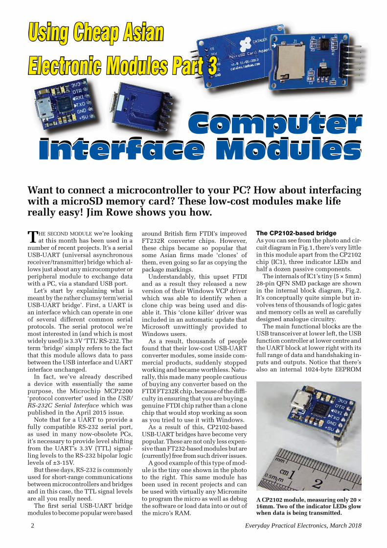
The CP2102-based bridgeAs you can see from the photo and cir-cuit diagram in Fig.1, there’s very little in this module apart from the CP2102 chip (IC1), three indicator LEDs and half a dozen passive components.
The internals of IC1’s tiny (5 × 5mm) 28-pin QFN SMD package are shown in the internal block diagram, Fig.2. It’s conceptually quite simple but in-volves tens of thousands of logic gates and memory cells as well as carefully designed analogue circuitry.
The main functional blocks are the USB transceiver at lower left, the USB function controller at lower centre and the UART block at lower right with its full range of data and handshaking in-puts and outputs. Notice that there’s also an internal 1024-byte EEPROM
A CP2102 module, measuring only 20 × 16mm. Two of the indicator LEDs glow when data is being transmitted.
Computer Interface Modules
Computer Interface Modules
Want to connect a microcontroller to your PC? How about interfacing with a microSD memory card? These low-cost modules make life really easy! Jim Rowe shows you how.
Using Cheap Asian Electronic Modules Part 3

Everyday Practical Electronics, March 2018
used to store the USB ID information: the vendor ID, the product ID, the se-rial number, the power descriptor, the release number and product descrip-tion strings.
In addition, there are two RAM buff-ers, one 640-byte USB transmit buffer and one 576-byte USB receive buffer.
Since the CP2102 has a calibrated 48MHz oscillator, it needs no exter-nal crystal to operate at the USB 2.0 full-speed rate of 12Mbps. Finally, it contains its own low drop-out (LDO) voltage regulator, to give an output of 3.3-3.45V from an input (REGIN) within the range 4.0-5.25V. This means that it can be powered directly from the USB VBUS line.
Circuit detailsWhile this regulator can supply up to 100mA, the circuitry within the chip itself draws only a little over 26mA (maximum) even in normal operation, and only 100�A when suspended. This means it can supply up to 70mA or so for external circuitry needing a 3.3V supply.
In short, the CP2102 is a very im-pressive chip. Now turn your attention back to the module’s circuit of Fig.1. There’s a micro-USB socket at the left (CON1) to connect to a PC’s USB port via a standard cable and also to power the module itself. So the VBUS line from pin 1 of the socket connects to pins 7, 8 and 9 of the CP2102, with 10�F and 100nF bypass capacitors.
Note that the module does not pro-vide connections to any of the CP2102 UART’s handshaking lines, except for DTR (‘data terminal ready’). However, this is unlikely to pose a problem for most applications nowadays, since even the DTR line is rarely used.
On the right-hand side there’s a 6-way pin header (CON2) for the UART input, output and handshaking (DTR) connections, plus the ground,
+5V and +3.3V power connections for use by external circuitry. There’s also a 100nF bypass capacitor on the +3.3V line, plus three small indicator LEDs, each with its own series resistor for current limiting.
LED1 is driven from pin 11 of the CP2102, the SUSPEND output, so it only glows when the device is not sus-pended by the host PC, ie, when it’s communicating with the PC normally via USB. On the other hand, LED2 and LED3 are connected between the +3.3V supply (pin 6) and pins 26 (TXD) and 25 (RXD) respectively, to indicate when data is being sent and received via the bridge.
LED1 draws a little over 1mA when it’s operating, while LED2 and LED3 will each draw about 5mA. Thus the LEDs could draw up to 11mA from the 3.3V supply (with full duplex serial communications, allowing LED2 and LED3 to light simultaneously) and this should be taken into account when fig-uring out how much reserve current is available for external circuitry.
How to use itUsing the CP2102 based USB-UART bridge module is very straightfor-ward. But before you can do so, you
may need to install a virtual COM port (VCP) driver on your PC. This is the software which takes care of buffer-ing data to and from the bridge and setting up the UART. In Windows, it makes the UART appear as if it were a legacy COM port.
You can get the right VCP driver from the Silicon Labs website: www.silabs.com/products/interface/Pages/interface-software.aspx
You can also download the latest version of the CP2102 data sheet from: www.silabs.com/support/Pages/docu-ment-library.aspx
When you go there you’ll find they can provide VCP drivers for not only Windows 7-10, but also for Windows 2000/XP/Vista/Server 2003, WinCE, Mac OS 9 and X, Linux (3.x.x and 2.6.x) and Android. They can also pro-vide drivers for direct ‘USB-Xpress’ interfacing to the PC, as an alternative to using the VCP approach.
Note that most modern operating systems, including Windows 10 and the latest versions of Mac OS X and Linux, should already have a suitable VCP driver installed. In this case, all you need to do is plug the bridge into a USB port and check that it has been recognised (eg, in Windows, check that a new COM port appears).
Once the driver is installed and working, you can set up your applica-tions to communicate with the module via the new COM port. That includes setting the correct baud rate and other options.
Of course, your circuitry on the UART side of the module needs to be connected to the appropriate pins on header CON2. These will usually be just the RXI, TXO and GND pins, al-though you might also want to make use of one of the power supply pins as well.
If you aren’t sure whether the bridge is working properly, the simplest way to test it is to wire up the RXI pin to the TXO pin. You can then open a ter-minal emulator, connect to that port
Fig.1: complete circuit diagram for the CP2102-based serial USB-UART bridge. The CP2102 can be powered directly from the USB VBUS line and it contains a low drop-out voltage regulator to provide 3.3-3.45V (VDD) from 4-5.25V (REGIN).
Fig.2: block diagram for the CP2102. This UART interface implements all RS-232 signals, including those for control and handshaking, although an external level shifter is required for full RS-232 compatibility.
Reproduced by arrangement with SILICON CHIP
magazine 2018.www.siliconchip.com.au

Everyday Practical Electronics, March 2018
and type on your keyboard. The typed characters should be sent back to you and appear in the terminal. If that works, but you still can’t communicate with your target device, check that the connections to its TX/RX pins are not swapped and also that you have set the right baud rate.
microSD card interfaceThere are many different adaptors for accessing an SD memory card from a
microcontroller or embedded module but they generally function in the same manner. The main differences are in terms of the card socket they provide and the chip(s) they use for interfacing.
The full circuit for this module is shown in Fig.3. Note that all SD cards can communicate via either serial peripheral interface (SPI) or a faster method, which consists of ei-ther a 4-bit parallel bus (older cards) or a high-speed differential interface
(UHS-compatible cards). The SPI method is by far the simplest to imple-ment with a microcontroller, unless it has a built-in SD card interface.
The other important thing to note is that all SD memory cards are in-tended to run from a 3.3V power supply and expect logic signals no higher than +3.3V. Some cards can only accept signals swinging over a smaller range, like 0-1.8V (UHS-I) or 0-0.4V (UHS-II).
Fig.3: full circuit of the SPI/microSD adaptor module. REG1 reduces the 5V (VCC) input supply from the host module to 3.3V, as required by microSD cards, while IC1 similarly reduces signal levels from the micro (which may run off 5V) to the 3.3V signal levels used by the SD card's I/Os.
Fig.4: internal block diagram of the SN74LV125A IC. When an OE input is pulled high, the corresponding output is disabled and has a high impedance.
C Port PC communications port, normally sending and
receiving data using the RS-232 serial protocol.
CS (Card C ip Se ect) used in an SPI bus to indicate when
the master wants to communicate with a slave (pulled low).
R ( ata ermina Read ) a ‘flow control’ signal which is
used to indicate when the serial port is ready to receive
data. Other, related flow-control signals include DSR (Data
Set Ready), CTS (Clear To Send) and RTS (Ready To Send).
PR ( ectrica rasea e, Pro ramma e Read n emor ) non-volatile memory that can be erased and
rewritten by applying a higher voltage than is used to read
data back. EEPROM is normally more robust than Flash.
L ( o drop out re u ator ) a regulator which can maintain
regulation with less than 2V between its input and output.
icromite: a Microchip PIC32 programmed with the
MMBasic interpreter.
S (master in, s a e out) the serial data line used to transmit
data from the selected slave to the master in an SPI bus.
S (master out, s a e in) the serial data line used to transmit
data from the master to the selected slave in an SPI bus.
( uad at o ead) a standard series of surface-mount
integrated circuit packages. As the name suggests, it is
attached to a PCB without through-holes via lands (pads)
on the bottom and sides of the package (ie, without leads).
RS 2 2 or 2 2 one of the most common standards for
serial communications. Used by the serial ports on older
PCs. Uses one wire for self-clocked data in each direction
plus optionally, several flow control signals.
R or R serial data receive line. Normally connected to TX
or TXD on the other device.
Seria Communication the process of transferring data one
bit at a time over a communication channel or bus.
SC (Seria C oc ) the shared clock line in an SPI bus, driven
by the master, typically up to 20MHz.
S (Secure i ita ) a non-volatile portable storage device
using Flash memory. Successor to MMC (MultiMedia Card).
SP (Seria Perip eria nter ace) a standard serial interface
bus, commonly used between a microcontroller and
peripherals such as SD cards. Unlike RS-232, SPI has
a separate clock line – ie, three wires for bidirectional
communications.
L ( ransistor ransistor Lo ic) refers to digital signals with
a 5V or (later) 3.3V amplitude, as used in early digital circuits.
or data transmission line. Normally connected to RX
or RXD on the other device.
R ( ni ersa s nc ronous Recei er ransmitter) circuit
to handle sending and receiving of serial data using one of
several different serial protocols or variations thereof.
S ( ni ersa Seria us) high-speed serial bus with power
(initially using four conductors) which replaced RS-
232 and parallel ports for interfacing a PC to pluggable
peripherals; from 1.5Mbps up to 5Gbps in latest version.
S ( tra i Speed) transfer speed for the latest SD
cards; up to 104MB/s for UHS-I, and 312MB/s for UHS-II.
VCP (Virtua C Port) a device driver that emulates an
RS-232 serial port over a different protocol such as USB.
Glossary

Everyday Practical Electronics, March 2018
Just because a chip has an SPI inter-face doesn’t mean it can necessarily interface directly with an SD card. If the micro operates from a 5V supply, its SPI port(s) may well provide and expect logic high signals above +3.3V. This means that the adaptor is needed both to drop the supply voltage down to 3.3V (assuming a suitable rail is not already available elsewhere) and also to act as a logic-level translator for the SPI signals.
The module shown here incorpo-rates LDO regulator REG1 to drop the +5V supply voltage from the micro (via J2) down to the +3.3V needed by both the microSD card at J1, and the single chip (IC1) on the module itself.
IC1 is an SN74LV125A tri-state buffer, to interface between the 5V logic levels (TTL) used on the micro side (via J2) and the low-voltage (0-3.3V) logic levels used on the SD card side (via J1). IC1 operates as a quad non-inverting buffer with tri-state outputs, ie, each output has its own OE (output enable low) input; see the internal block diagram of Fig.4. The OE inputs are not used, they are all tied to ground to enable the buffers permanently.
If you trace the signal paths through the circuit, you’ll see that the three outgoing signal lines from the micro’s SPI port at J2 (CS [card select], SCK [serial clock] and MOSI [data; mas-ter out, slave in]) each pass through a 3.3k� isolating resistor (to reduce ringing and provide some static elec-tricity protection) and then through one of the buffers in IC1 to reach the corresponding pin on SD card socket J1.
For example, the 5V MOSI signal enters via J2, passes through its 3.3k��resistor and then goes to buffer input 1A (pin 2). The low-voltage logic version of this signal then emerges from the 1Y output (pin 3) and runs to the MOSI pin of J1, the microSD card socket.
The SCK and CS signals are pro-cessed via IC1 buffers 2 and 3 in the same way. The path followed by the MISO (data; master in, slave out) signal is similar, the only difference
being that in this case the signal is travelling from the microSD card at J1 back to the micro at J2. Note though that the circuit does not level-shift this signal to 5V, so the micro will have to cope with a data input signal that only swings up to around 3.3V; most 5V micros are capable of this.
So the hardware side of the mod-ule is quite simple. Having said that, the SD card control protocol is quite complicated and so the software re-quired to drive it is far from trivial.
Putting it to useSince the module simply provides a transparent bridge linking the mi-croSD card to the SPI port of your mi-crocomputer, the software or firmware in the micro can exchange data with the card using the standard SPI com-mands. So with an Arduino, you can use commands like:
SPI.beginTransaction(SPISettings());receivedVal = SPI.transfer(val);SPI.end();
There’s also an Arduino code li-brary built into recent versions of the Arduino IDE, designed especially for reading from and writing to SD cards. It offers commands like begin(), mkdir(), open(), remove(), rmdir(), available(), close(), write() and read().
With a Micromite it’s also fairly straightforward, using commands such as:
SPI OPEN speed, mode, bitsreceived_data = SPI(data_to_send)SPI CLOSE
However, the Micromite Plus has built-in library commands specifi-cally intended for reading and writing to SD cards; see the recent articles on Micromite programming.
Useful links���Information on using standard SPI
commands with an Arduino, in-cluding some short examples, can be found at: www.arduino.cc/en/Reference/SD
���Details on using SPI communica-tions with a Micromite begin on page 92 of the Micromite manual: http://geoffg.net/Downloads/Micromite/ Micromite%20Manual.pdf
���An article on the SPI bus is avail-able at: http://en.wikipedia.org/wiki/Serial_Peripheral_Interface_Bus
���Wikipedia also has a very informa-tive article on the many kinds of SD cards, at: http://en.wikipedia.org/wiki/Secure_Digital
btbtthtm
This microSD module on a 43 × 24mm PCB is available from the SILICON CHIP online shop at: www.siliconchip.com.au/Shop/7/4019
- USB- Ethernet- Web server- Modbus- CNC (Mach3/4)- IO
- up to 256 microsteps- 50 V / 6 A����������� ����- Isolated
- up to 50MS/s- resolution up to 12bit- Lowest power consumption����������������������- 7 in 1: Oscilloscope, FFT, X/Y, ���� �� �������������� ��� ������������� ����������� ��� �
- up to 32 microsteps- 30 V / 2.5 A
�����- Encoders- LCD���������!�����"��!������"
www.poscope.com/epe
�����!������#$������!������%&�

1 www.handsontec.com
Handson Technology
User Guide
MicroSD Card Adapter Board
Not just a simple breakout board, this microSD adapter goes the extra mile – designed for ease of use.
SKU: MDU-1026
Brief Data:
Onboard 5V > 3V regulator provides 150mA for power-hungry cards.
3V level shifting means you can use this with ease on either 3V or 5V systems.
Uses a proper level shifting chip, not resistors: less problems, and faster read/write access.
Use 3 or 4 digital pins to read and write 2Gb+ of storage!
Four #2mm mounting holes.
Push-push socket with card slightly over the edge of the PCB so its easy to insert and remove.
Comes with 0.1″ right angle header pins so you can get it on a breadboard or use wires.

1 www.handsontec.com
Handson Technology
Data Specs
FT232R USB to Serial/TTL Interface Module
FT232R is a USB to serial UART interface. A low-cost way to add USB capability to
Arduino or other microcontrollers. Use this to give your own breadboard Arduino USB
capability for bootloading or downloading sketches. This board includes a DTR pin needed
to auto-reset Arduino when downloading to your device.
SKU: MDU-1066
Brief Data:
On Board Chip: FT232RL
Draw out all signal port of FT232RL chip
RXD / TXD transceiver communication indicator
USB power supply, can choose 5V or 3.3V, set by jumper
With over current protection, using 500mA self-restore fuse
Pin definition: DTR, RXD, TX, VCC, CTS, GND
Pitch: 2.54mm
Size: 36 x 18mm (L x W)
Interface: Mini USB

W
Everyday Practical Electronics, April 2018 33
The device is designed to run from 3.3-5.5V DC, with operation from 5V recommended. It has a nominal current drain of 1.5mA when meas-uring, or 50μA when in standby. It needs at least two seconds between measurements.
The AM2302/DHT22/RHT03 module measures only 25.1 × 15.1 × 7.7mm, while the PCB for the most common module using it measures 39 × 23mm – see our picture.
The sensor has four connection pins, although one is labelled ‘NC’ (no con-nection) in Aosong’s data sheet.
As you can see from Fig.2, there’s very little in a typical sensing mod-ule apart from the AM2302/DHT22/RHT03 device itself.
There are just two passive compo-nents on the board: a 100nF bypass capacitor from VCC to ground and a 4.7k� pull-up resistor between the digital data bus line and VCC.
The reason for that resistor leads us to discuss the way the device commu-nicates with an external micro, over that single-wire bus.
How it handles dataAlthough it’s poorly explained in the AM2302 data sheet, here’s the basic idea: when the DATA line is allowed to float at the logic high level (pulled high by the 4.7k� resistor), the sensor effectively sleeps in standby mode. To
VCC
GND
START SIGNAL FROM MICRO
BUS RELEASEDFOR 20 sμ
(1ms RECOMMENDED)
SENSORRESPONSE
SIGNAL
80 sμ 80 sμ
LOGIC HIGH
LOGIC LOW
FORMAT OF START REQUEST SIGNAL FROM MICRO,'OK WILL START' RESPONSE FROM AM2302 SENSOR
Fig.4: the micro differentiates between what type of bit it has received based on the pulse time; a data bit of value zero has a pulse time of 78μs while a one has a pulse time of 120μs.
VCC
GND
CODING FOR DATA BIT 0' ' CODING FOR DATA BIT 1' '
50 sμ
28 sμ
50 sμ
70 sμ
LOGIC HIGH
LOGIC LOW
DATA BIT CODING FOR 'READ' SIGNALS FROM AM2302
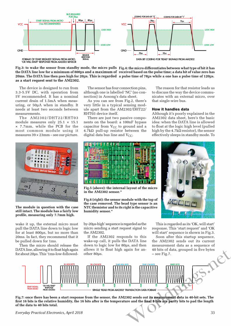
Fig.3: to wake the sensor from standby mode, the micro pulls the DATA line low for a minimum of 800μs and a maximum of 20ms. The DATA line then goes high for 20μs. This is regarded as a start request sent to the AM2302.
The module in question with the case still intact. The module has a fairly low profile, measuring only 7.7mm high.
Fig.5 (above): the internal layout of the micro in the AM2302 sensor.*
Fig.6 (right): the sensor module with the top of the case removed. The bead type sensor is an NTC themistor and to its right is the capacitive humidity sensor.*
wake it up, the external micro must pull the DATA line down to logic low for at least 800μs, but no more than 20ms. In fact, they recommend that it be pulled down for 1ms.
Then the micro should release the DATA line, allowing it to float high again for about 20μs. This ‘1ms-low-followed-
by-20μs-high’ sequence is regarded as the micro sending a start request signal to the AM2302.
If the AM2302 responds to this wake-up call, it pulls the DATA line down to logic low for 80μs, and then allows it to float high again for an-other 80μs.
This is regarded as its ‘OK, will start’ response. This ‘start request’ and ‘OK will start’ sequence is shown in Fig.3.
Soon after this startup sequence, the AM2302 sends out its current measurement data as a sequence of 40 bits of data, grouped in five bytes – see Fig.7.
START SIGNALFROM MICRO
'OK WILL START'RESPONSE
FROM AM2302
RH HIGH BYTE RH LOW BYTE TEMP HIGH BYTE TEMP LOW BYTE PARITY BYTE
MSB
MSB
MSB
MSB
MSBLSB
LSB
LSB
LSB
LSB
SINGLE 'READ FROM AM2302' TRANSACTION DATA FORMAT
Fig.7: once there has been a start response from the sensor, the AM2302 sends out its measurement data in 40-bit sets. The first 16 bits is the relative humidity, the 16 bits after is the temperature and the final 8 bits are parity bits to pad the length of the data to 40 bits total.
Worl
dmags
.net
mags.n
mMS
M
d
LSBSBmm
BB
mdmag
its measurement dataeasurement e final 8 bits are parity8 bits are pa

34 Everyday Practical Electronics, April 2018
The relative humidity reading is in the first two bytes (RH HIGH and RH LOW), followed by the temperature reading in the next two bytes (TEMP HIGH and TEMP LOW), and finally there’s a checksum or parity byte to allow error checking.
All of these bytes are sent MSB (most-significant bit) first and LSB (least-significant bit) last.
It’s also worth noting that both the RH and temperature readings have a resolution of 16 bits.
While this single-wire-bus transac-tion may look fairly straightforward, it isn’t quite that simple – because of the special encoding that Aosong uses for the data bits themselves.
As shown in Fig.4, a binary zero is coded as a logic low of 50μs followed by a logic high of 28μs, whereas a bi-nary one is coded as the same logic low of 50μs, but followed by a logic high of 70μs.
So both a zero and a one begin with a logic low lasting for 50μs, but a logic high that follows lasts for only 28μs in the case of a zero rather than 70μs in the case of a one.
As a consequence, data bits with a value of 0 last for a total of 78μs, while those with a value of 1 last for 120μs. So the time taken by each of those data bytes as shown in Fig.7 will not be fixed, but will vary, depending on the data bit values.
For example, a byte consisting of all zeroes (00000000) will last for only 624μs, while a byte of all ones (11111111) will last for 960μs. So in practice, the duration of each data byte will vary between 624 and 960μs.
The micro connected to the AM2302 needs to take this rather unusual coding system into account when it decodes RH and temperature data.
How it’s usedYou shouldn’t have to worry about decoding the AM2302 measurement data yourself, because many people have already worked it out for most of the popular microcontroller.
For example, if you want to hook up an AM2302-based module to a Micro-mite, Geoff Graham has already solved this problem and provided a special command in his MMBasic program-ming language. It looks like this:
HUMID pin, tVar, hVar
Where HUMID is the command key-word and ‘pin’ is the micro’s I/O pin to which the module’s DATA line is connected.
‘tVar’ is the name of the floating-point variable you want to receive the returned temperature (in °C) and ‘hVar’ is the name of a second
floating-point variable to receive the returned relative humidity (as a percentage). It’s that easy!
If you’re running the module from a 5V supply, you do have to make sure that you connect the module’s DATA line to a Micromite pin that is 5V tolerant – ie, one of pins 14 to 18, 21 or 22 on the 28-pin Micromite.
So if you have connected the module’s DATA line to pin 18 of the Micromite and have declared the temperature and RH variables as say ‘temp!’ and ‘RH!’ respectively, you’ll be able to read the sensor’s data with this one-line command:
HUMID 18, temp!, RH!
If you want to take a sequence of say 10 readings spaced apart by the recom-mended minimum of two seconds and print them to the console, here’s the kind of simple program you’ll need:
DIM nbr% = 10 DIM temp! = 0.0 DIM RH! = 0.0 PAUSE 1000 DO HUMID 18, temp!, RH!
PRINT “Temperature = “temp! “C & humidity = “ RH! “%” nbr% = nbr% - 1 PAUSE 2000 LOOP UNTIL nbr% = 0
If you want to hook up an AM2302-based module to any of the Arduino ver-sions, it’s almost as easy. You have quite a choice when it comes to pre-written applications, some of which you’ll find using these github.com links:
http://bit.ly/2DJHJ2Ohttp://bit.ly/2BBrAKUhttp://bit.ly/2BBgju3
There are also sample programs on both of these websites:
www.aosong.comwww.humidity.com
So it’s not at all difficult to use one of these low cost AM2302/DHT22/RHT03-based modules with a readily available microcontroller.
* These pictures have been taken from the video at:
http://youtu.be/C7uS1OJccKI
by www.youtube.com/user/electronupdate
Reproduced by arrangement with SILICON CHIP
magazine 2018.www.siliconchip.com.au
- USB- Ethernet- Web server- Modbus- CNC (Mach3/4)- IO
- up to 256 microsteps- 50 V / 6 A����������� ����- Isolated
- up to 50MS/s- resolution up to 12bit- Lowest power consumption����������������������- 7 in 1: Oscilloscope, FFT, X/Y, ���� �� �������������� ��� ������������� ����������� ��� �
- up to 32 microsteps- 30 V / 2.5 A
�����- Encoders- LCD���������!�����"��!������"
www.poscope.com/epe
�����!������#$������!������%&�
Worl
dEveryday Everyd
Wo
Woorl
dmagn up to 12bit
Lowest power con��������������
- 7 in 1: Oscil���� �� ��������
gsanet

1 www.handsontec.com
Handson Technology
User Guide
DHT11 Humidity & Temperature Sensor Module
DHT11 Temperature & Humidity Sensor features a temperature & humidity sensor with
calibrated digital output. By using the exclusive digital-signal-acquisition technique and
temperature & humidity sensing technology, it ensures high reliability and excellent long-
term stability. This sensor includes a resistive-type humidity measurement component and an
NTC temperature measurement component with 8-bit microcontroller, offering excellent
quality, fast response, anti-interference ability and cost-effectiveness.
SKU: SSR-1006
Brief Data:
Operating voltage: 3.5~5.5V.
Humidity Range: 20~90% ± 5%.
Humidity Resolution: 1%.
Temperature Range: 0~50℃ ± 1℃.
Temperature Resolution: 1℃.
Operating Current: 3mA (Max).
Standby: 0.15mA.
Sampling Period: 1s.
Mounting Hole: M3.
2.54mm breadboard friendly header pin connector.
LCD modules with two lines of 16 characters have been around for
many years and we’ve used them in numerous projects. They are also now much cheaper thanks to their popular-ity for use with Arduino, Micromite and the Raspberry Pi.
However, many of these Arduino and other microcontrollers are a lit-tle limited when it comes to I/O pins, which means that the six or seven pins required to interface to a standard LCD module can leave you with too few pins to interface with other systems and components.
This problem can be solved by using an LCD with a serial interface, or alter-natively, attaching a small piggy-back module to a parallel LCD to provide serial/parallel translation.
By using a piggy-back module that communicates using the 2-wire I2C protocol, you end up with an LCD that can be driven using just two wires: one for the serial data (SDA) and the other for the serial clock (SCK). That’s apart from the ground and power wires (typi-cally +5V).
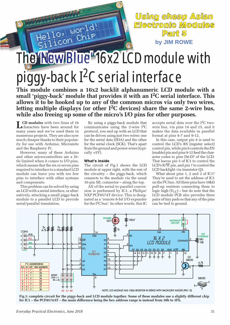
What’s insideThe circuit of Fig.1 shows the LCD module at upper right, with the rest of the circuitry – the piggy-back, which connects to the module via the usual 16-pin SIL connector – along the top.
All of the serial-to-parallel conver-sion is performed by IC1, a Philips/NXP PCF8574T device. This is desig-nated as a ‘remote 8-bit I/O expander for the I2C bus’. In other words, this IC
accepts serial data over the I2C two-wire bus, via pins 14 and 15, and it makes the data available in parallel format at pins 4-7 and 9-12.
In this case, output pin 4 is used to control the LCD’s RS (register select) control pin, while pin 6 controls the EN (enable) pin and pins 9-12 feed the char-acter codes to pins D4-D7 of the LCD. That leaves pin 5 of IC1 to control the LCD’s R/W pin, and pin 7 to control the LCD backlight via transistor Q1.
What about pins 1, 2 and 3 of IC1? They’re used to set the address of IC1 on the I2C bus. All three pins have 10k� pull-up resistors connecting them to logic high (VCC) – but do note that the LCD module PCB also provides three pairs of tiny pads so that any of the pins can be tied to ground.
Using cheap Asian Electronic Modules
Part 5
This module combines a 16x2 backlit alphanumeric LCD module with a small ‘piggy-back’ module that provides it with an I2C serial interface. This allows it to be hooked up to any of the common micros via only two wires, letting multiple displays (or other I2C devices) share the same 2-wire bus, while also freeing up some of the micro’s I/O pins for other purposes.
The ‘New Blue’ 16x2 LCD module with piggy-back I2C serial interface
by JIM ROWE
IC1PCF8574T
IC1PCF8574T
A2
Vss
Vdd
P1
INT
SDA
SCL
P7
P6
P5
P4
P3
P2
A01
2
3
4
5
6
7
8
9
10
11
12
13
14
15
16
A1
P0
C
BE
1
2
3
4
5
6
7891011121314D0D1D2D3D4D5D6D7 GND
CONTRAST
R/W
EN
RS
Vdd15
16
ABL
KBL
2x4.7k
3x10k 1k
VR110k
4.7k
LCDCONTRAST
Q1S8050
100nF
A0A1A2
CON1
1
2
3
4VCC
SDA
SCL
GND
I C ADDRESSINGA2 A1 A0 HEX ADDRESS
2
11110000
11001100
10101010
2726252423222120
(LINKSOUT = 1
IN = 0)
λ BACKLIGHTON/OFF
LED1
A
K
POWER
NOTE: LCD MODULE HAS 100 RESISTOR IN SERIES WITH BACKLIGHT ANODE (PIN 15)Ω
J3Y CB
E
S8050
16 x 2LCD MODULE
Fig.1: complete circuit for the piggy-back and LCD module together. Some of these modules use a slightly different chip for IC1 – the PCF8574AT – the main difference being the hex address range is instead from 38h to 3Fh.
Everyday Practical Electronics, June 2018 31

This allows the chip’s I2C address to be set to any hexadecimal value be-tween 0x20 (32) and 0x27 (39), just by bridging the pairs of pads, as shown in the small table at lower left in Fig.1.
So the default I2C address of the piggy-back module (and thus LCD) is 0x27 with all links out, but this can be changed to 0x20 simply by fitting all three links, or to any address in between by fitting one or two links. This allows a number of the LCD-piggyback combi-nations to be connected to the same I2C bus, with each one given a different I2C address so that the micro driving the bus can send data to any one it chooses.
Other I2C devices can reside on the same bus (eg, temperature sensors, memories, other microcontrollers), as long as you ensure that no two devices have the same address.
There are some serial I2C LCD mod-ules that use a slightly different chip for IC1, the PCF8574AT. This is virtually identical to the PCF8574T shown in Fig.1, except that the I2C address range is between 0x38 and 0x3F.
By using a combination of the two chips, up to 16 different serial I2C LCDs may be connected to the same I2C bus, provided you use eight with the PCF8574T bridge chip and eight with the PCF8574AT chip.
Fig.1 also shows that the piggy-back has a power-on indicator (LED1), a 2-pin SIL connector and jumper shunt that can be used to disable the LCD’s backlight if not required. Trimpot VR1 can be used to adjust LCD contrast in the usual way (via pin 3).
Note that the SDA and SCL lines con-necting between pins 1 and 2 of CON1 and pins 14 and 15 of IC1 are each fitted with a 4.7k� pull-up resistor, as the I2C bus uses active-low logic. These resis-tors can be left in place if the module is the only slave connected to the I2C bus. However, if you’re going to be hooking up other I2C slave devices to the same bus, all but one should have the SDA and SCL pull-up resistors removed.
Using itThis type of module really needs to be hooked up to a micro, and that turns out to be fairly easy to do with any of the popular options available.
All you have to do is connect the VCC and ground pins to a suitable volt-age source (which may be the same one that’s powering the micro) and the SDA and SCL pins to the I2C bus pins on the microcontroller. Fig.2 shows how this is done with an Arduino Uno or a compatible like the Duinotech Classic. It couldn’t be much simpler.
By the way, although the SDA and SCL pins of the LCD module are shown in Fig.2 connected to the
ADC4/SDA and ADC5/SCL pins at up-per right on the Arduino, they could instead be connected to the pins marked SDA and SCL on the other side of the Arduino down near the USB connec-tor. On most Arduino boards, these pin pairs are connected in parallel.
It’s just as easy to connect the serial I2C LCD module to a Micromite, as you can see from Fig.3.
Connecting the module up to a micro is only half the story. Then you have to work out how to get the micro to send it the data you want displayed.
The complicating factor here is that quite a few people have written ‘li-braries’ to make it easier to drive this kind of serial I2C LCD module from an Arduino sketch, by providing a set of simple function calls like:
lcd.print(“Text”);This is all very well, but even though most of these library files have the name LiquidCrystal_I2C.h, they are often dif-ferent in terms of their finer details and compatibility with any particular serial I2C LCD module.
Rather than you going through the same sort of hassles we did to find a suitable library, we’ll simply point
you at some that we found to work. These are available at the following Github links:
http://bit.ly/2sHf6Cdhttp://bit.ly/2sLrpxm
It’s possible that these are actually the same library, because in one place we found the author listed as Frank de Brabander but the maintainer as Marco Schwartz. We found both through the following website: www.arduinolibrar-ies.info/libraries/
Anyway, these libraries do seem to work with the module shown, as you’ll find out by downloading the ‘Hello World’ sketch (HelloWorld.ino) from the EPE website (www.epemag.com) and running it. We’ve included a copy of the library (as a ZIP file) within the package. The resulting display is shown in the adjacent photo.
Don’t forget to change the I2C address shown in the sketch (0x27) to 0x3F (= 3Fh), if your piggy-back module is fitted with a PCF8574AT instead of a PCF8574T. You’ll also have to change this address if you’ve changed the address using the three small pairs of pads.
������������ ����� ��� �� �������������� ����������� �� ��������� ����������������� ���� ������� ����� �� ���������� �! ���������� ��"��"������ ������� ��� �����������#"������������ �$�����"%�� ���� &�������� �� �� �����'"(�)�� "��� ������ *� &������+�"+,� �� ���� �� �'�� �"� �������� ���������� ������� ������� ������ �� ������� ���� ���������� �������������������
-�������,'�)��,'�*���� &���� �������+�++�+�������������%������ �������� �'������������������� � ������ �������� ����������������". ������������ �������� ���� &������/�"+��� �������� ���� �������������������������� ����� �0����+�+�1���2�/3"+�2���2�/+"+�1�#�2�+�1�, �'����� � ���� �4567��������8����� � &������#93,������ ��������+�++++��++�++++���������
Reading hexadecimal numbers
ARDUINO UNO,FREETRONICSELEVEN ORDUINOTECH
CLASSIC
IO0/RXD
IO1/TXD
IO2/PWM
IO3/PWM
IO5/PWM
IO6/PWM
IO4/PWM
IO7
IO8
IO9/PWM/MOSI
IO10/PWM/MISO
IO11/PWM/SCLK
IO12
IO13
USB
TYP
E B
MIC
RO
GND
AREF
SDA
SCL
ADC0
ADC1
ADC2
ADC3
ADC4/SDA
ADC5/SCL
+5V
+5V
GND
GND
VIN
RESET
+3.3V
DC
VO
LTS
INPU
T
16 x 2 LCD16 x 2 LCD
GND
SDA
SCL
VCC
LCD WITH I2C SERIAL BACKPACK
ARDUINO UNO,FREETRONICSELEVEN ORDUINOTECH
CLASSIC Fig.2: pin connections for the LCD and piggy-back module to an Arduino or compatible device. Instead of passing the SDA/SCL to the ADC4/ADC5 pins on the Arduino, it can be connected to the SDA and SCL on the other side of the Arduino. For most Arduino boards, these pins are normally connected in parallel.
32 Everyday Practical Electronics, June 2018

Everyday Practical Electronics, June 2018 33
How about a Micromite?Programming a Micromite to talk to the I2C LCD module is not quite as easy as with an Arduino, as currently the inbuilt MMBasic LCD commands only support the parallel interface. You will find a program called I2CLCD.bas in the MMBasic Library, which can be downloaded in zipped-up form from the bottom of this page: http://geoffg.net/maximite.html#Downloads
However, this program was written for a piggy-back module with a different configuration than the one which most piggy-backs seem to use (and we have shown in Fig.1). Then there’s a further issue in that the I2C command syntax has changed as MMBasic has evolved. As a result, we ended up having to re-write the software completely.
Changing the program’s commands to suit the different connections between the PCF8574T bridge chip and the LCD module itself wasn’t too hard. The major difficulty was in getting the program to initialise the LCD’s controller correctly.
The correct set-up commands have to be sent to it soon after power is applied, and these commands have to be sent in a particular order, with pauses between them to allow the controller to process them before the next command arrives for correct operation.
using the PCF8574AT chip instead of the PCF8574T. Look for this line near the start:
M S N E E 2 dd & 2 ��)'/1'+1'�1+*
All you need to do is change ‘&H27’ into the correct address for your module. This program provides a good starting point for writing your own MMBasic programs using an I2C LCD. It’s fairly well commented, so you should be able to see how to adapt the program to dis-play other things.
The underside of the LCD module’s PCB has the piggy-back module (black) located above it. The jumper shunt located on the piggy-back module can be used to disable the LCD backlighting if it’s not needed.
$ �� �����D ����� ������ � ������ ������� �0�������5����E���� �0�������������������&�� ���� �� �� ���������� �
'�� ���� ��������������������������� ) ��� � � "�� ��� �� �� ������ � �� � �� ��*� ��� 4�� ���'��7�� �����������/�×#����� �25�F56�������������� ������� ��� ������� �+G×/���� �
-� ������"��D��������������D������/�×/����+G×#���. ������� ��� F56��� ��� � �� �� � � ���� ��������������� ���� �������. �
here bu
16 x 2 LCD16 x 2 LCD
GND
SDA
SCL
VCC
LCD WITH I2C SERIAL BACKPACK
GND
RESET
3
4
5
9
10
14
16
MICROMITEMICROMITE17
18
21
22
24
25
26
+3.3V
+5V
(SDA)
(SCL)
Fig.3: pin connections for the LCD and piggy-back module to a Micromite.
The top of the LCD module. The screen is mounted on a PCB measuring 80 × 36mm, while the visible area of the LCD measures 64 × 14.5mm.
0��� �������� �� � ��������� � ��� ������ � �� )��� �� �:���/�+9� ���� *��� �� �� ��� �� �������� �������� ���������� �� ���@04"@'!-����� � ����� � �� �� ��� �� � 5;/+�/� � ��� � -���� �� � ��� � �� ��������� �� � �� � � � ������� �� ��� �� � :��� /�+9� ���� �� ���� ���� �� ��� ���� �� ��� � E� � ��� ���� ���� �� ��� � ����"@04� ���D �� ��� �� � @04� �������� ������ �� ��� ������ ���������������. ���� �'�@04������>������������� ���� ������ ����������������������������������@04���� �'������� �'� �� ���������
-� ���� ����� �� �)���������H*���������� ����� ������������ ��������������� �0�F����� ��������� ���� � �������� ������ � � ��� ��� ��� ���� � ��� �� � ���� � ����� � 0�� �D � �� � ���� ���� ����� ��� �� ����� ����0�F��������� ��������� ���������� ����� ������ ������������������ �� ��� �
erial R bridge m dule an her ersi n
After downloading as much informa-tion as we could find regarding the cor-rect initialisation sequence and timing for the Hitachi HD44780U and Samsung KS0066U LCD controller chips (which seem to be the two most commonly used in current alphanumeric LCD modules), we were finally able to get the program working correctly and reliably. We found this website most helpful: http://web.alfredstate.edu/weimandn/lcd/lcd/lcd_initialization/
Basically, our program (called JRI-2CLCD.bas) just displays a ‘Hello, world!’ message over and over on the LCD; just like the one for the Ardui-no. You can download this from our website, open it in MMEdit and then upload it to your Micromite and you should get the same display as shown in the photos.
As with the Arduino sketch, you may need to change the I2C address given for your display’s piggy-back, if it has some of the address links fitted or is
Reproduced by arrangement
with SILICON CHIP
magazine 2018.
www.siliconchip.com.au

1 www.handsontec.com
Handson Technology
User Guide
I2C to LCD Interface Board By using this little I2C to LCD interface board, we can control the LCD using only 2 wires, and not worry about resistors to adjust the contrast since it’s all included. Usually, Arduino LCD display projects will run out of pin resources easily, especially with Arduino Uno. And it is also very complicated with the wire soldering and connection. This I2C LCD Interface board use an I2C communication interface. It means it only needs 4 pins for the LCD display: VCC, GND, SDA, SCL. It will save at least 4 digital / analog pins on Arduino. All connector are standard 0.1” /2.54mm (Breadboard type). You can connect with jumper wire directly.
SKU: MDU-1042
• Compatible with Arduino Board or other controller board with I2C bus.
Brief Data:
• Interface to HD44780 compatible LCD Modules with various screen size. • I2C Address:0x20-0x27(0x20 default) • Supply voltage: 5V • Interface: I2C to 4bits LCD data and control lines. • Adjustable contrast • Board Size: 42x19 mm.

1 www.handsontec.com
Handson Technology
User Guide
I2C Serial Interface 20x4 LCD Module
This is I2C interface 20x4 LCD display module, a new high-quality 4 line 20 character LCD module with on-board
contrast control adjustment, backlight and I2C communication interface. For Arduino beginners, no more cumbersome
and complex LCD driver circuit connection. The real significance advantages of this I2C Serial LCD module will
simplify the circuit connection, save some I/O pins on Arduino board, simplified firmware development with widely
available Arduino library.
SKU: DSP-1165
Brief Data:
Compatible with Arduino Board or other controller board with I2C bus.
Display Type: Black on yellow green backlight.
I2C Address:0x38-0x3F (0x3F default)
Supply voltage: 5V
Interface: I2C to 4bits LCD data and control lines.
Contrast Adjustment : built-in Potentiometer.
Backlight Control: Firmware or jumper wire.
Board Size: 98x60 mm.
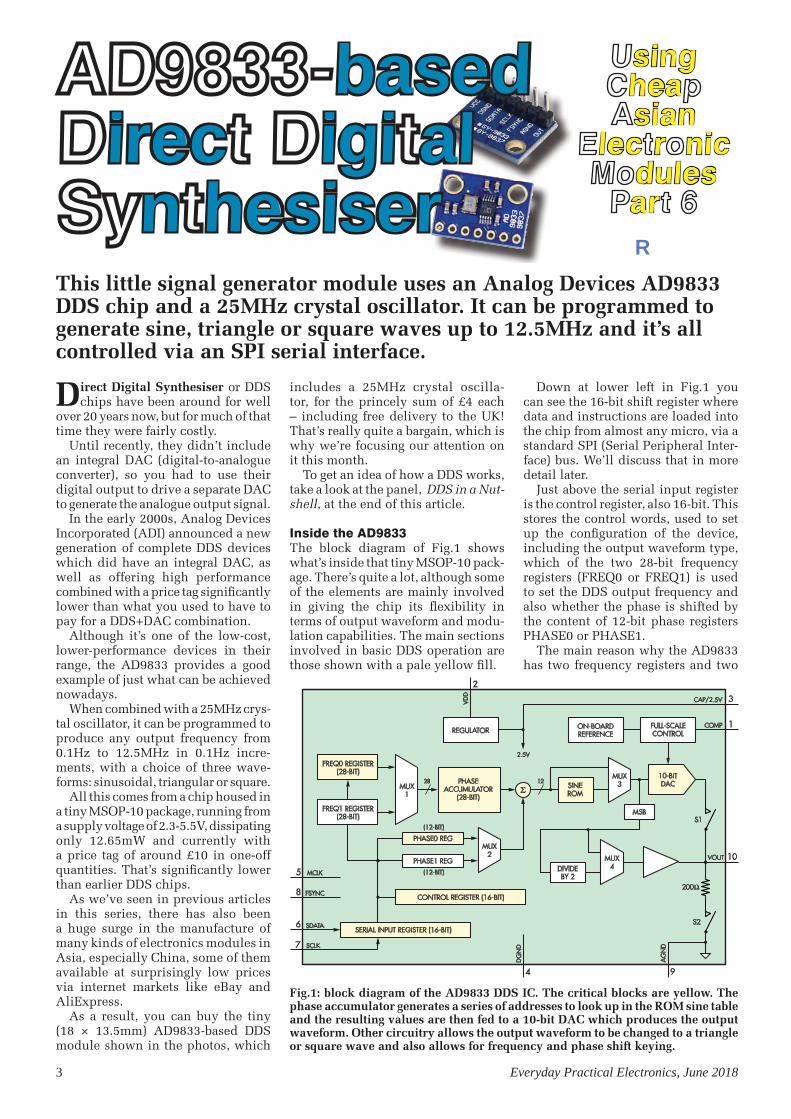
3 Everyday Practical Electronics, June 2018
Direct Digital Synthesiser or DDS chips have been around for well
over 20 years now, but for much of that time they were fairly costly.
Until recently, they didn’t include an integral DAC (digital-to-analogue converter), so you had to use their digital output to drive a separate DAC to generate the analogue output signal.
In the early 2000s, Analog Devices Incorporated (ADI) announced a new generation of complete DDS devices which did have an integral DAC, as well as offering high performance combined with a price tag significantly lower than what you used to have to pay for a DDS+DAC combination.
Although it’s one of the low-cost, lower-performance devices in their range, the AD9833 provides a good example of just what can be achieved nowadays.
When combined with a 25MHz crys-tal oscillator, it can be programmed to produce any output frequency from 0.1Hz to 12.5MHz in 0.1Hz incre-ments, with a choice of three wave-forms: sinusoidal, triangular or square.
All this comes from a chip housed in a tiny MSOP-10 package, running from a supply voltage of 2.3-5.5V, dissipating only 12.65mW and currently with a price tag of around £10 in one-off quantities. That’s significantly lower than earlier DDS chips.
As we’ve seen in previous articles in this series, there has also been a huge surge in the manufacture of many kinds of electronics modules in Asia, especially China, some of them available at surprisingly low prices via internet markets like eBay and AliExpress.
As a result, you can buy the tiny (18 × 13.5mm) AD9833-based DDS module shown in the photos, which
includes a 25MHz crystal oscilla-tor, for the princely sum of £4 each – including free delivery to the UK! That’s really quite a bargain, which is why we’re focusing our attention on it this month.
To get an idea of how a DDS works, take a look at the panel, DDS in a Nut-shell, at the end of this article.
Inside the AD9833The block diagram of Fig.1 shows what’s inside that tiny MSOP-10 pack-age. There’s quite a lot, although some of the elements are mainly involved in giving the chip its flexibility in terms of output waveform and modu-lation capabilities. The main sections involved in basic DDS operation are those shown with a pale yellow fill.
Down at lower left in Fig.1 you can see the 16-bit shift register where data and instructions are loaded into the chip from almost any micro, via a standard SPI (Serial Peripheral Inter-face) bus. We’ll discuss that in more detail later.
Just above the serial input register is the control register, also 16-bit. This stores the control words, used to set up the configuration of the device, including the output waveform type, which of the two 28-bit frequency registers (FREQ0 or FREQ1) is used to set the DDS output frequency and also whether the phase is shifted by the content of 12-bit phase registers PHASE0 or PHASE1.
The main reason why the AD9833 has two frequency registers and two
This little signal generator module uses an Analog Devices AD9833 DDS chip and a 25MHz crystal oscillator. It can be programmed to generate sine, triangle or square waves up to 12.5MHz and it’s all controlled via an SPI serial interface.
based irec igi al n hesiser
singheasian
lec r nicdulesar
R
PHASEACCUMULATOR
(28-BIT)
FREQ0 REGISTER(28-BIT)
FREQ1 REGISTER(28-BIT)
MUX1
MUX3
MUX2 MUX
4
SINEROMΣ
122810-BITDAC
MSB
DIVIDEBY 2
200Ω
1
2
3
4
5
6
7
8
9
10VOUT
FULL-SCALECONTROL
COMPON-BOARDREFERENCEREGULATOR
PHASE0 REG
PHASE1 REG
(12-BIT)
(12-BIT)
SERIAL INPUT REGISTER (16-BIT)
CONTROL REGISTER (16-BIT)
2.5V
CAP/2.5V
SDATA
SCLK
FSYNC
MCLK
VD
D
AG
ND
DG
ND
S1
S2
Fig.1: block diagram of the AD9833 DDS IC. The critical blocks are yellow. The phase accumulator generates a series of addresses to look up in the ROM sine table and the resulting values are then fed to a 10-bit DAC which produces the output waveform. Other circuitry allows the output waveform to be changed to a triangle or square wave and also allows for frequency and phase shift keying.

Everyday Practical Electronics, June 2018 3
phase registers is to give it the capabil-ity of generating signals with frequen-cy-shift keying (FSK) or phase-shift keying (PSK) modulation. Multiplex-ers MUX1 and MUX2 allow these op-tions to be controlled using bits in the control register.
So how are those 28-bit frequency/phase increment registers FREQ0 and FREQ1 loaded with 28-bit data from the 16-bit serial input register? This is done by sending the data in two 14-bit halves, in consecutive 16-bit words from the micro, with the lower half first and then the upper half.
The AD9833 can be configured to accept the data this way sim-ply by manipulating two bits in the control register. The same bits can also be used to configure it for setting either the lower or higher 14-bit ‘half word’ alone, which can be useful for some applications (such as frequency sweeping).
MUX3, MUX4 and switches S1 and S2 are all controlled by further bits in the control register. MUX3 simply allows the sine ROM to be bypassed, with the output from the phase accu-mulator fed directly to the DAC. This is how the AD9833 produces a trian-gle wave output, since the amplitude of a triangle wave is a linear function of its phase.
For a square wave output, the DAC is disconnected from the chip’s analogue output (pin 10) using integrated switch S1, and instead makes use of the MSB (most-significant bit) output of MUX3. This automatically gives a square wave output and MUX4 allows you to divide its frequency by two, if needed.
The integrated 200� resistor con-nected between the analogue output pin and ground via switch S2 is used to convert the DAC’s output current into a proportional voltage output. Since S2 is controlled in parallel with S1, this means that when S1 cuts the link between the DAC output and pin 10, S2 also removes the built-in 200� output shunt.
This makes the chip’s output volt-age swing in square-wave mode significantly higher than for the sine or triangular (DAC-derived) options.
To be specific, the square wave out-put is around 5.2V peak to peak, while for sine or triangular waves the output drops to around 650mV peak-to-peak.
The complete moduleNow refer to Fig.2, which shows the complete circuit for the 18 × 13.5mm module shown in the photo opposite.
It simply comprises the AD9833 DDS chip (IC1) and its equally tiny (3 × 2.2mm) 25MHz crystal oscilla-tor. There are six even smaller SMD
capacitors, most of them used for fil-tering either the power supply rails or IC1’s VOUT pin.
Seven-way SIL connector CON1 is used to make all of the signal and power connections to the module. Pins 1 and 2 are used to provide the module with 5V power, while pins 3-5 are used to convey the SPI commands and data to IC1 from the micro you’re using to control it. And pins 6 and 7 are used to carry the analogue output signal from IC1 out to wherever it’s to be used.
LimitationsBefore we talk about driving the mod-ule from a micro like an Arduino or a Micromite, we should discuss its limitations.
First, the aforementioned difference in output amplitude for square wave versus sine/triangle waves is a factor of about eight times, or 18dB. So if you want to use the module as the heart of a function generator, you will need to attenuate the square wave output by 18dB, to match the sine and triangle output levels.
You will also need to pass the sine and triangular outputs through a low-pass filter with a corner frequency of around 12-15MHz, to remove most of the DAC switching transients. After this processing, the outputs can all pass through a common buffer amplifier and output attenuator system.
You don’t need to wor-ry about any of these ni-ceties if you simply want to use the module as a programmable clock sig-nal source. You can just program it to generate a square wave output and use it as is.
Another limitation, as noted in the DDS in
a Nutshell box, is that the maximum output frequency is half the sampling clock frequency; in this case, 12.5MHz. But because of the way a DDS works, it can only produce a clean square wave at this maximum frequency.
If you want to get a reasonably smooth sine or triangular wave output, this will only be possible at frequencies below about 20% of the clock frequency, or in this case, a maximum of about 5MHz.
Programming itWhen your program starts up, it will need to carry out a number of set-up tasks. These include:1. Declare the micro’s pins to be used
by the SPI interface and set them to their idle state (typically high).
2. Start the SPI interface, configured for a clock rate of say 5MHz, the data to be sent MSB (most-significant bit) first and using clock/data timing mode 2 (10 binary). If possible, it should also be set for the data to be exchanged in 16-bit words rather than bytes.
3. Send initialisation commands to the AD9833 to set up its control register, the FREQ0 register and the PHASE0 register. These involve sending the
1
2
3
4
5
6
7
SCLK
FSYNC
VOUT
SDATA
1
23
4
25MHzXTAL OSC
25MHzXTAL OSC
OUT
VCC EN
GND
100nF
100nF
10nF
SDATA
DGND
VDD
SCLK
AGND
VOUT CAP/2.5V
MCLK
1
2
3
4
5
6
7
8
9
10
FSYNC
IC1AD9833
IC1AD9833
COMP
22pF
4.7 Fμ 100nFCON1
DGND
AGND
VCC
VCC
Fig.2: circuit of the AD9833-based DDS module used in this article. The AD9833 IC and 25MHz crystal oscillator plus a few passive components are mounted on a small PCB, with a SIL header to make control and output connections.
The DDS module is shown at approximately twice actual size to provide greater clarity. From left to right, the pin connections are VCC, DGND, SDATA, SCLK, FSYNC, AGND and VOUT.

3 Everyday Practical Electronics, June 2018
following five 16-bit words (shown here in hexadecimal):
• 0x2100 (resets all registers, sets control register for loading fre-quency registers via two 14-bit words)
• 0x69F1 (lower word to set FREQ0 for 1000Hz)
• 0x4000 (upper word to set FREQ0 for 1000Hz)
• 0xC000 (writes 000 into PHASE0 register)
• 0x2000 (write to control register to begin normal operation)
With that, the DDS should produce a 1000Hz sinewave. To change to one of the other waveforms, you need to send the correct code to the control register. To change the output frequency, you need to send the appropriate pair of 14-bit words to one of the frequency registers. Note that these are sent lower word first, then upper word.
To make programming the AD9833 a little easier, the basic coding for the control, frequency and phase registers is summarised in Fig.3. I also have written a couple of simple example programs to illustrate programming
the AD9833 module; more about these shortly. First, you’ll need to know how the module can be connected to one of the popular micros.
Driving it from an ArduinoFig.4 shows how to connect the mod-ule up to almost any Arduino or Ar-duino clone.
This takes advantage of the fact that most of the connections needed for interfacing to an SPI peripheral are made available on the 6-pin ICSP header that is fitted to most Arduino variants.
D0D1D2D3D4D5D6D7D8D9D10D11D12D13D14D15
MODEDIV2OPBITEN
SLEEP12
SLEEP1
RESETPHASESEL.
FREQSEL.HLBB280 00 0 00
D1D3D5D6D7D8D10D11D12D130/1 D40/1 D9 D0D2
D1D3D5D6D7D8D10D111 1 D40/1 D9 D0D2
TO WRITE TO THE CONTROL REGISTER:
TO WRITE TO A FREQUENCY REGISTER:
TO WRITE TO A PHASE REGISTER:
AD9833 SERIAL INPUT WORD FORMAT:
MSB LSB
CONTROLREGISTERADDRESS
FREQUENCY REGISTER WRITEMODE: 1= WRITE AS TWOSUCCESSIVE 14-BIT WORDS0= WRITE SINGLE 14-BITWORD INTO MSB (HLB = 1)OR LSB (HLB = 0) HALVES OFFREQUENCY REGISTER
HIGH OR LOW BITS SELECT:1= MSB BITS, 0 = LSB BITS
FREQUENCY REGISTER SELECT:0 = FREQ0 REG, 1 = FREQ1 REG
FREQ. REGISTERADDRESS:
01 = FREQ0,10 = FREQ1
PHASE REGISTERADDRESS:
110 = PHASE REG0,111 = PHASE REG1
PHASE REGISTER SELECT:0 = PHASE0 REG, 1 = PHASE1 REG
RESET INTERNAL REGISTERS:0 = NORMAL OPERATION, 1 = RESET
MODE:0 = SINEWAVE
1 = TRIANGULAR
DAC DATA MSB:1 = NO DIVISION,
0 = DIVIDE BY 2
CONTROLS WHETHER DAC OUTPUTIS CONNECTED TO VOUT OR NOT:
0 = CONNECTED (SINE OR TRIANGLE),1 = DISCONNECTED (SQUARE WAVE)
DAC POWER SAVING MODE:0 = DAC POWERED UP, ACTIVE,
1 = DAC POWERED DOWN
MCLK ENABLE BIT:0 = MCLK ENABLED (NORMAL OPERATION)
1 = MCLK DISABLED (DAC OUTPUT CONSTANT)
14 BITS OF DATA
12 BITS OF DATA
X
Scope 1 (above): a 1000Hz sinewave generated using an Arduino programmed with AD9833_DDS_module_test.ino
Fig.3 (left): the format of the 16-bit digital control data sent to the AD9833. The top two bits determine whether the remaining 14 bits are used to update the frequency, phase or control registers. The control register is used to change the output waveform type, switch between two different sets of frequencies and phases or go into a low-power sleep mode.
The underside of the DDS module with the 7-pin male header attached. Again, it’s shown twice actual size, due to its small size (18 × 13.5mm).
MOSI
SCK
SS
SS
ARDUINO UNO OR NANO,FREETRONICS ELEVEN OR LEOSTICK,DUINOTECH CLASSIC OR NANO, ETC
ARDUINO UNO OR NANO,FREETRONICS ELEVEN OR LEOSTICK,DUINOTECH CLASSIC OR NANO, ETC
IO0/
RXD
IO1/
TXD
IO2/
PWM
IO3/
PWM
IO5/
PWM
IO6/
PWM
IO4/
PWM
IO7
IO8
IO9/
PWM
IO10
/SS
IO11
/MO
SI
IO12
/MIS
O
IO13
/SC
K
USB TYPE BMICRO
GN
D
ARE
F
SDA
SCL
AD
C0
AD
C1
AD
C2
AD
C3
AD
C4/
SDA
AD
C5/
SCL
+5V
+5V
GN
D
GN
D
VIN
RESE
T
+3.3
VDC VOLTSINPUT
1 2
3 4
5 6
ICSP
SCKSCK
MISOMISO
MOSIMOSI
+5V+5V
GNDGNDRSTRST
OUT
AGND
FSYNC
SCLK
SDATA
DGND
VCC
AD9833BASEDDDS
MODULE
AD9833BASEDDDS
MODULE
SINE, TRIANGULAROR SQUARE WAVE OUTTO LP FILTER, BUFFER &
ATTENUATORFig.4: hooking the AD9833-based DDS module up to an Arduino. It mainly involves making SPI connections via the 6-pin programming header.

Everyday Practical Electronics, June 2018 3
The connections to the ICSP header are quite consistent over just about all Arduino variants, including the Uno, Leonardo and Nano, the Freetronics Eleven and LeoStick, and the Duino-tech Classic or Nano.
In fact, the only connection that’s not available via the ICSP header is the one for SS/CS/FSYNC, which needs to be connected to the IO10/SS pin of an Arduino Uno, Freetro-nics Eleven or Duinotech Classic, as shown in Fig.4.
With other variants, you should be able to find the corresponding pin without too much trouble. Even if you can’t, the pin reference can be changed in your software sketch to match the pin you do elect to use.
Arduino sample programOne of my sample programs written for an Arduino is called, AD9833_DDS_module_test.ino
It simply initialises the AD9833, starts generating a 1000Hz sinewave (Scope 1) and then changes the wave-form after five seconds, giving you a triangular wave (Scope 2), then a square wave (Scope 3) and finally a half-frequency square wave, before returning to a sinewave and repeating the sequence. If you look at the code, you can see just how easy it is to con-trol an AD9833 DDS module from an Arduino.
Driving it from a MicromiteFig.5, on the next page, shows how to drive the module from a Micromite. By connecting the MOSI, SCK and SS/FSYNC lines to Micromite pins 3, 25 and 22 as shown, MMBasic’s built-in SPI protocol commands will have no trouble in communicating with the module.
One thing to note is that if you want to drive the AD9833 module from a Micromite in a BackPack that is already connected to an LCD touch-screen, there’s a small complication
arising from the fact that the LCD touchscreen also communicates with the Micromite via its SPI port.
To prevent a conflict, your program needs to open the SPI port immediately before it sends commands or data to the module, and then close the port again immediately afterwards.
Micromite sample programMy other program is written for the Micromite, specifically, the Micro-mite LCD BackPack. It’s called, Sim-ple AD9833 FnGen.bas
This one is a little more complicated and lets you control the AD9833’s output frequency as well as the wave-form, simply by using buttons and a virtual keypad on the Micromite’s touch screen. It’s quite easy to drive, and again, should show you how the AD9833 can be controlled via a Micromite.
Both this program and the Arduino program are available for download from the EPE website.
Alternative moduleIn the April issue, we published a Micromite-based DDS Function Gen-erator project by Geoff Graham, which also uses the AD9833. Geoff has used a slightly different module which in-cludes the ability to vary the output level and also has a low-impedance buffered output.
The module Geoff has used is shown overleaf, to the left of its circuit dia-gram, Fig.6. It differs from the simpler module in that it has the output signal from the AD9833 fed to a separate SIL connector.
From there, the signal is routed to an MCP41010 10k� digital potentio-meter IC via a 0� resistor, which acts as a digitally controlled attenuator. The output of this attenuator is fed to an AD8051 rail-to-rail op amp and together these constitute a PGA, or ‘programmable gain amplifier’ (not pin grid array).
The digital pot also communicates via SPI, and in fact its clock and data pins are wired up in parallel with the AD9833’s, so it is on the same SPI bus.
The only difference in communi-cation is rather than pulling the FSY pin low, as you do to communicate with the AD9833, you pull the CS pin low to communicate with the MCP41010.
Like the AD9833, the MCP41010 is controlled by writing 16-bit data words to it. For the MCP41010, the bottom eight bits of the data are the new po-tentiometer position, while the upper eight bits contain two command bits, two channel selection bits and four ‘don’t care’ bits, which it ignores.
The command bits allow you to select whether you are setting the pot wiper position or commanding the IC to go into a power-down mode.
We suggest you check its datasheet for details; however, you really only need to send one of two different com-mands to this device when using this module:
0x11xy – set wiper position to 8-bit value xy0x2100 – shut down potentiome-ter, saving power and disabling the output signal
For example, the command 0x11FF will set the output level to maximum, command 0x1180 will set the output level to 50% and 0x1101 will set it to the minimum non-zero level.
The attenuated output signal is available at pin 6 and this goes to the non-inverting input of an AD8051 high-frequency op amp, which is configured with a gain of six times, providing an output swing of around 3V peak-to-peak for sine and triangle waves. This signal is fed to both a 2-pin header connector and SMA socket via another 0� resistor.
Other variations in this module are that it has 100� protection resistors for the four control pin inputs, the
Scope 2 and 3: a 1000Hz triangular (left) and square (right) wave produced by running the AD9833_DDS_module_test.ino file on an Arduino or compatible device. Note the higher amplitude of the square wave output.

3 Everyday Practical Electronics, June 2018
supply for the 25MHz crystal oscil-lator has a 10� isolating resistor that also forms a low-pass filter in com-bination with the added 4.7μF ce-ramic capacitor, and there is a 2-pin header which makes the output of the
AD9833 available, before it enters the attenuator.
There are more details on how to use this module in April’s article on the Mi-cromite-based DDS Function Genera-tor, but besides needing to program the
digital pot with the attenuation value, its control is pretty much identical to the description above.
Final commentsDan Amos has designed a ‘Touch-screen Function Generator’ us-ing an AD9833 module driven by a Micromite with an LCD Back-Pack, and he has also added a digi-tal potentiometer, an output buffer amplifier and even an incremental encoder for adjusting either the output frequency or its amplitude.
He has provided the MMBasic source code for his program, and a user manual as a PDF file – both of which can be downloaded from the EPE web-site. That project and its software is an excellent example to get you started on using the AD9833 DDS module.
One last comment – as well as be-ing able to generate fixed frequency, FSK and PSK modulated signals, the AD9833 can also be programmed to generate swept-frequency signals.
In fact, the Micromite DDS Function
GND
RESET
3
4
5
9
10
14
16
MICROMITEMICROMITE17
18
21
22
24
25
26
+3.3V
+5V
MOSI
SCK
MOSI
SCK
SS
SS
(MISO)
OUT
AGND
FSYNC
SCLK
SDATA
DGND
VCC
AD9833BASEDDDS
MODULE
AD9833BASEDDDS
MODULE
SINE, TRIANGULAROR SQUARE WAVE OUT
TO LP FILTER, BUFFER& ATTENUATOR
Fig.5: connecting the module to a Micromite is easy; all you need to do is wire up its two power pins, the three SPI pins and the signal output connections.
Direct Digital Synthesis (DDS) in a nutshellThis simplified explanation should give you some insight into how a DDS works. A DDS is based around one or more look-up tables stored in read-only memory (ROM). These contain a set of high-resolution digi-tal samples of a single wave cycle.
Let’s consider the case where the table contains a sinewave.
The values from the ROM table are fed to a DAC (digital-to-analogue converter), so that for each entry in the table, the DAC will produce an analogue DC voltage corresponding to the value of the sample stored in that address.
As a result, if a counter is used to cycle through the table entries continuously, the DAC output is a continuous sinewave.
Let’s say the table contains 1000 entries which represent a single sine-wave cycle and the counter which indexes the table is incremented at a rate of 1MHz. This means that the output will be a sinewave at 1MHz ÷ 1000 = 1kHz. By changing the rate at which the counter increases, we can change the output frequency.
Since the DDS chip operates from a fixed external clock, in order to vary the rate at which the DDS runs
through its ROM table, a fancier counter configuration known as a ‘phase accumulator’ is used. This is shown in Fig.7 and it consists of a binary adder feeding an accumu-lator register.
The important point to note is that the phase accumulator register has 28 bits of precision while the sample table, with 4096 entries, only requires a 12-bit number to index its entries.
Hence there are an additional 16 bits of fractional phase data in the register and these effectively indicate output phase values in-between those represented by the values in the table.
The binary adder has two 28-bit inputs, one of which is the current phase value from the accumulator register. The other input comes from the frequency register at far left, also 28 bits wide.
This is the register which we use to set the DDS output frequency. At each clock cycle, the value in the frequency register is added to the value in the accumulator register and this result is stored back in the accumulator register. As a result, as long as the frequency register value doesn’t change, the accumu-lator register increases by the same amount on each clock cycle.
With a 28-bit phase accumulator register, a value of zero indicates a
28-BITACCUMULATOR
REGISTER
BINARYADDER
+ 10-BITDAC ANALOG
OUTPUT
PHASE ACCUMULATOR
FREQUENCYPROGRAMMING
28
28
28 28
28
12 10
28
MASTER CLOCKINPUT
28-BITFREQUENCY
REGISTER4096 ENTRYWAVEFORM
SAMPLETABLEROM( )
Fig.7: the basic layout of a simple DDS. The Phase Accumulator adds the contents of the frequency register to the accumulator register on each clock cycle. The top 12 bits of the accumulator register is then used
to look up an entry in the waveform table ROM, producing a 10-bit digital amplitude value which is subsequently fed to the digital-to-analog converter (DAC) to generate the analog output signal.

Everyday Practical Electronics, June 2018 3
1
2
3
4
5
6
CLK
DAT
CS
FSY
1
23
4
25MHzXTAL OSC
25MHzXTAL OSC
OUT
VCC EN
GND
100nF
10nF
SDATA
DGND
VDD
SCLK
AGND
CAP/2.5V VOUT
MCLK
1
2
10
4
5
6
7
8
9
3
FSYNC IC1AD9833
IC1AD9833
COMP
22pF
4.7 Fμ 100nF
DGND
VCC
VCC
4 x 100Ω
8
47
5
MCP41010MCP41010
PB0
PA0 VDD
GND
6PW0
3
42
15
1
2AGND
PGA
5k
1k
100nF AD8051AD8051
1CS
3SI
2SCK
0Ω
0Ω
1
2AGND
VOUT
4.7 Fμ100nF
10Ω
Fig.6: the circuit of the alternative DDS module shown above, which is also widely available. This one incorporates an MCP41010 digital potentiometer to allow the output amplitude to be controlled as well as an AD8051 high-speed op amp buffer to keep the output impedance low and provide some gain to allow a higher maximum output signal level. The module is shown at aproximately 1.5 times its actual size of 32 × 32mm.
Generator in April’s issue does just that, so refer to that article for more details on frequency sweeping.
phase in radians of zero while its max-imum value of 228 – 1 (268,435,455) represents a phase of just under 2�.
When the value of the accumula-tor register exceeds 228 – 1, it rolls back around to zero, hence main-taining 0 < phase < 2�. Each time it ‘rolls over’, that represents one complete cycle from the output.
With a frequency register value of 1, it will take 228 clock cycles for this to happen. With a master clock of 25MHz, that means the output frequency will be 25MHz ÷ 228 = 0.09313Hz or just under 0.1Hz.
With a frequency register value of 2, it will take 228 ÷ 2 clock cycles to roll over, giving an output frequency of 25MHz ÷ 227 = 0.186Hz and so on. So the output frequency resolution with this configuration is just under 0.1Hz.
But how are such low frequencies possible with only a 4096-entry table? Well, only the top 12 bits of the 28-bit accumulator register are used to index the ROM table.
This means with the minimum frequency value of one, it will only roll over to the next entry in the table once every 2(28–12) = 65,536 clock cycles. Hence, each value from the table is sent to the DAC 65,536 times before progressing to the next one, giving a very low frequency.
At higher frequencies, in this case above 25MHz ÷ 4096 (6.103kHz),
values in the table will be skipped when necessary in order to increase the output frequency. In other words, the counter which indexes the table may increase at a rate of 1, 2, 3, 4 times per clock, or some-where in-between, by skipping the occasional table entry.
For example, to produce an out-put of 12.207kHz, every second entry from the ROM table is sent to the DAC (12.207kHz = 25MHz ÷ [4096 ÷ 2]).
Based on the above, we can calcu-late the output frequency as:
h cl RacFor the DDS shown in the diagram, with a 28-bit phase accumulator having a resolution (Rac) of 228 (= 268,435,456) and with a master clock frequency (Mclk) of 25MHz, this simplifies down to:
h (We’re showing the table with 4096 entries, but note that due to symmetry, it is only necessary to store the values representing a quarter of a sinewave.)
The second quadrant of a sine-wave is a mirror-image of the first, so this can be achieved by running through a quarter sine table back-wards, while the third and fourth quadrant are simply an inverted version of the first and second, and these can be obtained by negating the
values from the first two quadrants.You’ll also notice that the sam-
ples stored in the ROM are shown as having a resolution of 10 bits, to suit the 10-bit DAC, which can pro-duce an analogue output with 1024 different voltage levels.
One more thing to bear in mind. Because a DDS achieves higher output frequencies by skipping samples in the waveform ROM, at higher output frequencies, the sam-pling resolution effectively drops.
This continues until you reach the ‘Nyquist frequency’ of half the master clock frequency (ie, 12.5MHz) above which the output from the DAC actually starts to drop in frequency.
So the theoretical maximum fre-quency for a DDS is half that of the master clock.
But in practice, because of the above, if you want a reason-ably smooth sinewave output that doesn’t need too much low-pass filtering, it’s a good idea to limit the maximum output frequency to about 20% of the master clock frequency; say 5MHz for a 25MHz master clock.
Reproduced by arrangement with SILICON CHIP
magazine 2018.www.siliconchip.com.au

When I first noticed this type of 8×8 LED matrix display
module being offered on eBay and AliExpress, I must confess that I didn’t get overly excited. Sure, they were very cheap – but what could you actually use an 8x8 LED matrix display for? All I could think of was displaying a few pretty patterns. Fun, perhaps, but not all that useful.
Despite this ho-hum first impres-sion, I decided to order a couple of the modules just to see if they had any other uses. And when they arrived, I discovered that they did.
The data sheet for the MAX7219 controller chip is available from Max-im’s website (http://bit.ly/2I5Rz1Q) and indicates that it has primarily been designed to drive an 8-digit 7-segment LED display. In fact, the ability to drive an 8x8 LED matrix is in many ways just a bonus feature!
Inside the MAX7219To understand the dual personality of the MAX7219, take a quick look at the block diagram in Fig.1. As you can see, there’s more inside this modest-looking 24-pin DIP device than you might have expected.
Down at the bottom, you can see the 16-bit shift register where data and instructions are shifted into the chip from almost any micro, via a standard SPI (Serial Peripheral Inter-face) bus. Above the eight least-sig-nificant bits (D0-D7) is an eight-byte dual-port SRAM, where the display data is stored.
Four more bits, D8-D11, are decoded to determine whether the data in the lower eight bits of the shift register is to be loaded into one of the addresses in the display SRAM (either with or without further decoding), or into one of the control registers to set the chip’s operating modes.
Five registers control shutdown, the mode, intensity, scan limit and display test.
The shutdown register blanks the display when power is first applied or at a later time, to reduce the power consumption. It can also be used to flash the display on and off, for ‘alarm’ situations. During normal operation, data bit D0 of this register is set to one.
The mode register is used to control whether the data in the SRAM regis-ters for each digit is to be decoded (according to ‘CODE B’) or used as-is. The interesting point here is that the
mode register can be set for decoding all eight digits, none of them or virtu-ally any combination in between.
So for driving an 8×8 LED matrix, for example, you wouldn’t use the decoding features, while for driving an 8-digit 7-segment display you’d program it to decode all eight registers.
But you could also use it to drive a 6-digit 7-segment display by decoding just those six digits, with the remaining two digit positions either unused or used without decoding to drive other indicator LEDs. So it’s quite flexible.
The intensity register provides pro-grammable digital control over the brightness of the LEDs. As you can see from Fig.1, the chip has a segment current reference circuit (at upper left), controlled by the current fed in via the ISET pin (pin 18).
The peak current sourced from the chip’s segment driver outputs (upper right) is nominally 100 times the cur-rent entering the ISET pin, which is normally connected to the +5V supply rail via a resistor of 9.53k� or more. The module shown in the pictures uses a 10k� resistor.
At the same time, the value stored in bits D0-D3 of the intensity control register determines the duty cycle of the chip’s internal pulse-width mod-ulator, and hence the display bright-ness. The duty cycle is a 4-bit value, meaning that there are 16 different programmable duty cycle/brightness levels, from 1/32 (3%) to 31/32 (97%).
This low-cost module uses a Maxim MAX7219 serial LED display chip and comes complete with a plug-in 8x8 LED matrix display. However, the MAX7219 is equally capable of driving an 8-digit 7-segment LED display, and its SPI interface allows it to be driven by a microcontroller using only three wires, meaning both the module and the chip are surprisingly flexible.
SPI 8x8 LED Matrix Display Module
Using Cheap Asian Electronic Modules Part 7: by Jim Rowe
This very cheap module includes the MAX7219 IC and a plug-in 8×8 LED matrix display.
34 Everyday Practical Electronics, July 2018

wired to CON2 and CON3 of the mod-ule instead of an 8×8 LED matrix. Note that for space reasons, we haven’t shown the MAX7219 chip or the rest of the module circuitry to the left of CON2 and CON3 in Fig.5, but these are all exactly the same as in Fig.4.
In fact, the only changes needed to drive a pair of 4×7-segment displays instead of an 8×8 LED matrix with the MAX7219 module are in software rather than hardware.
Specifically, it’s just a matter of enabling decoding for all eight digits, instead of disabling it, as required for driving the 8x8 LED matrix.
This leads us to hooking the MAX7219 module up to popular mi-cros and programming it to display what you want. In fact, not only is it possible to drive an 8-digit display using a MAX7219, pre-built modules are available on eBay and AliExpress. These incorporate a PCB with an SMD MAX7219 on the back and two 4-digit 7-segment displays plugged into head-er sockets on the front. Like the 8x8 matrix displays, they have 6-pin con-nectors at each end to wire up to your micro and also allow daisy chaining.
Driving them from an ArduinoAs shown in Fig.6, it’s quite easy to connect these modules up to almost any Arduino or Arduino clone, by tak-ing advantage of the fact that most of the connections needed for interfacing to an SPI peripheral are made available on the 6-pin ICSP header fitted to most Arduino variants.
The connections to the ICSP header are fairly consistent over just about all Arduino variants, including the Uno, Leonardo and Nano, the Freetronics Eleven and LeoStick, and the Duino-tech Classic or Nano.
In fact the only connection that’s not available via the ICSP header is the one for SS/CS/LOAD, which needs
Then there’s the scan limit control register, which is basically used to de-termine how many digits are scanned by the display multiplexing circuitry. This allows the chip to be programmed for any number of display digits be-tween one and eight.
Do note that Maxim warns in the datasheet that if three or fewer digits are selected, the resistor connected to the chip’s ISET pin should be increased in value to reduce the power dissipa-tion in the digit drivers.
Finally, there’s the display test control register, which can be used to switch between normal opera-tion and the test mode, where all segments are lit in order to test the display itself.
To help you put all of these func-tions of the MAX7219 into perspec-tive, Fig.2 summarises the decoding of register address bits D8-D11, while Fig.3 shows the significance of data bits D0-D7 when segment decoding (ie, ‘CODE B’) is enabled (A) or decoding is disabled (B).
Driving the 8x8 LED matrixSo that’s a quick run-down on the MAX7219 device and its internal working. Fig.4 shows the full circuit for the module as it arrives, and it has everything needed to drive the 8x8 LED matrix directly from a micro like an Arduino or a Micromite.
There’s very little to the module apart from the MAX7219 (IC1), the 8x8 LED matrix and the two 8-pin connec-tors (CON2 and CON3) used to join them together.
There are two 5-pin SIL connectors; one used for the supply and serial bus inputs (CON1) and the other for the matching outputs (CON4) used for daisy-chaining further modules, plus the 10k� resistor connected to IC1’s ISET pin and a pair of bypass capaci-tors on the 5V supply line, one 100nF and one 10μF electrolytic.
Programming it to produce inter-esting patterns turns out to be fairly straightforward, as we’ll see shortly. But before we do so, you’ll recall that I mentioned earlier that the MAX7219 was originally intended for driving 7-segment LED displays of up to eight digits.
Driving 8-digit 7-segment displaysThis configuration is shown in Fig.5, with a pair of 4×7-segment displays
DIN DOUT
CLK
D0 D1 D2 D3 D4 D5 D6 D7 D8 D9 D10 D11 D12 D13 D14 D15
DIG
IT D
RIVE
RS
D7
D6
D5
D4
D3
D2
D1
D0
SEG
MEN
T D
RIVE
RS
SEG A
SEG B
SEG C
SEG D
SEG E
SEG F
SEG G
SEG DP
SEGMENTCURRENT
REFERENCE
ISET
8 x 8–DUAL PORT
SRAM
ADDRESSREGISTERDECODER
LOAD
8
88
8
8
4
CODE ROMBWITH BYPASS SHUTDOWN REG.
MODE REGISTER
INTENSITY REG.
SCAN LIMIT REG- .
DISPLAY TEST REG.
MULTIPLEXSCAN
CIRCUITRY
INTENSITYPULSEWIDTH
MODULATOR
( )MSB
Fig.1: internal block diagram of the MAX7219 IC. The 8-byte dual-port SRAM is used to store the current LED state, while the decoder block simplifies the software required to drive a 7-segment display. The segment drivers supply a fixed current determined by the current flow out of the ISET pin, and intensity is modulated by PWM applied by those same segment drivers.
D0D1D2D3D4D5D6D7D8D9D10D11D12D13D14D15
DATA BITSREGISTERADDRESS BITS
DON CARE’T
X X X X
X X X X
X X X X
X X X X
X X X X
X X X X
X X X X
X X X X
X X X X
X X X X
X X X X
X X X X
X X X X
X X X X
0
0
0
0
0
0
0
0
1
1
1
1
1
1
0
0
0
0
1
1
1
1
0
0
0
0
1
1
0
0
1
1
0
0
1
1
0
0
1
1
0
1
0
1
0
1
0
1
0
1
0
1
0
1
0
1
= NO OP
= 0DIGIT
= 1DIGIT
= 2DIGIT
= 3DIGIT
= 4DIGIT
= 5DIGIT
= 6DIGIT
= 7DIGIT
= DECODE MODE
= INTENSITY
= SCAN LIMIT
= SHUTDOWN
= DISPLAY TEST
(X0 hex)
(X1 hex)
(X2 hex)
(X3 hex)
(X4 hex)
(X5 hex)
(X6 hex)
(X7 hex)
(X8 hex)
(X9 hex)
( hex)XA
( hex)XB
( hex)XC
( hex)XF
Fig.2: data is sent to the MAX7219 over a serial bus, 16 bits at a time. This table shows how bits 8-11 determine which register is written to, while bits 0-7 contain the new data for that register. With bits 8-11 set to a value between 1 and 8, one of the entries in the dual-port SRAM is updated while values of between 9 and 12 or 15 are used to write to one of the five control registers.
Everyday Practical Electronics, July 2018 35

IC1MAX7219
IC1MAX7219
1
2
3
4
5
6
7
8
9
10
11
12
14
15
16
17SEG DP
SEG G
SEG A
SEG B
DIG4
DIG3
Vcc
GND GND
18
19
20
21
22
23
24
13DIN
SEG E
DIG5CLK
SEG C
ISET
LOAD CS( )
SEG D
DIG0
DIG2
DIG6
DOUT
DIG1
DIG7
SEG F
1088 8x8AS LED MATRIX
100nF
10k�
CON1
CON2
VCC VCC
GND GND
DATA IN DATA OUT
CLK CLK
CS CS
10 F�
CON3
CON4
1
2
3
4
5
6
7
8
9
10
11
12
13
14
15
16
SEG DP
SEG G
SEG F
SEG E
SEG D
SEG C
SEG B
SEG A
DIG 0
DIG 1
DIG 2
DIG 3
DIG 4
DIG 5
DIG 6
DIG 7
1 2
3
4
5
6
789
10
11
12
13
14
15
16
Above is the layout of the module without the 7-segment display and below in Fig.4 is the matching circuit diagram.
Fig.3 (left): when ‘Code B’ decoding is active for a segment, the lower four bits of the value for that segment form a look-up table for one of 16 possible 7-segment display configurations, as shown at right. The top bit determines whether the decimal point is lit. Compare this to (B) at bottom, where decoding is not active and the eight bits in SRAM control the segment drivers directly.
Fig.4 (below): the circuit of a typical pre-built 8×8 LED matrix module with MAX7219 driver. A photo of this type of module is shown above. There’s virtually nothing to it, just the LED matrix display module, the MAX7219 IC and some connectors to join them together and to provide connections to the microcontroller and optionally, more daisy-chained LED displays.
to be connected to the IO10/SS pin of an Arduino Uno, Freetronics Eleven or Duinotech Classic, as shown in Fig.6.
With other variants, you should be able to find the corresponding
pin without too much trouble – and even if you can’t find it, the pin ref-erence can be changed in your soft-ware sketch to match the pin which you decide to use.
Driving them from a MicromiteIt’s also quite easy to drive these modules from a Micromite, using the connections shown in Fig.7. By connecting the MOSI, SCK and SS/
3 Everyday Practical Electronics, July 2018

LOAD lines to Micromite pins 3, 25 and 22 as shown, MMBasic’s built-in SPI protocol commands will have no trouble in communicating with the module.
So that’s the basic story regarding the hardware side of the MAX7219-based module which can drive either an 8x8 LED matrix array or eight 7- segment LED displays.
Before we finish, a few words are in order regarding the software side, ie, how to write programs to get the mod-ule to display what you want.
Writing the softwareThe basic idea here is that when your program starts up, it needs to carry out a number of set-up tasks:• Declare the micro’s pins that are
going to be used by the SPI inter-face and set them to their idle state (normally high).
• Start up the SPI interface, with its settings configured for a clock rate of say 5MHz, the data to be sent MSB (most-significant bit) first and using clock/data timing mode 0. If possible, it should also be set for
the data to be exchanged in 16-bit words rather than bytes.
• Send the initialisation commands to the MAX7219 to set up its five control registers: shutdown, decode mode, intensity, scan limit and dis-play test.
After these tasks have been done, you should be able to send out the actual display data for each of the 8-digit display addresses in the MAX7219’s SRAM. And if the display is to be a dynamic one, you
Fig.5: the circuit of a typical pre-built 8-digit 7-segment common-cathode LED display using a MAX7219. Pre-built modules for this configuration are also available. We haven’t shown the IC itself, as its configuration is identical to that of Fig.4 – all that’s changed is that in place of the 8x8 LED matrix are two 4-digit 7-segment displays with the anodes wired in parallel.
Fig.6: connecting either type of MAX7219-based module to an Arduino is easy. Simply wire up the SPI pins and power supply to the ICSP header on the Arduino and the CS pin to a free GPIO – ideally IO10, which is the hardware slave select (SS) pin.
Reproduced by arrangement with SILICON CHIP
magazine 2018.www.siliconchip.com.au
Everyday Practical Electronics, July 2018 37

can send out revised data at the appropriate times.
To help you understand what’s in-volved in writing your own programs for the module, I have written a couple of simple example programs which repeatedly display an expanding star pattern on the 8x8 LED matrix array (you can see the fully expanded star on the lead photo).
One of these programs is written for Arduino and I have called it: sketch2_
for_Testing_MAX7219.ino. The other program is written for the Micromite, and is called MAX7219 LED array Star.bas Both of these programs are available for download from the EPE website.
Both programs simply blank the display for a second or so, then cause a small square pattern to appear first in the centre of the array and then expand out fairly quickly to form a star, with its tips at the four corners of
the array. The expanded star remains visible for about three seconds before the array is blanked again and the sequence repeats.
It’s all quite simple, but either pro-gram should give you a reasonably clear guide regarding how to use the MAX7219 display driver module in your own projects.
I’ve tried to provide a lot of explana-tory comments in both programs, to help in this regard.
GND
RESET
3
4
5
9
10
14
16
MICROMITEMICROMITE17
18
21
22
24
25
26
+3.3V
+5V
MOSI
SCK
VCC VCCGND GNDDATA IN DATA OUTCS CSCLK CLK
MAX BASED72198x8 LED MATRIXDRIVER MODULE
TO O
THER
MO
DU
LES
MOSI
SCKSS
SS
( )MISO
Fig.7 (left): wiring a MAX7219 module to a Micromite is simply a matter of connecting the 5V, GND and 3-wire SPI bus between the two units. The MOSI and SCK pins on the Micromite are fixed (and may vary between different types of Micromite) while slave select (SS) can go to pretty much any digital output pin.
Directly below – you can see the underside of the module is sparse, only having the markings for the connections to and from the module.
3 Everyday Practical Electronics, July 2018
www.eshop.icsat.co.uk
Supporting Education
Supporting
Electronics & Robotics for Makers
ICSAT’s Pixie system for Education and Hobbyists now adds ATTiny basedmainboards to the PICAXE and Genie based versions.
Pixie 8 & 14 mainboards, simple standalone boards thatprovides one or two standard Pixie port connectors for
power and I/O connections. PICAXE andGenie versions have the 3.5mm downloadsocket and the ATTiny versions have theATMEL 6 pin ICSP programming connector.
Pixie Sprite is a complete module with I/Oconnections and 2 bidirectional motor out-puts powered by an L293D, and is availablein all 3 chip types: PICAXE, Genie andAttiny84. The board can use crocodile clipsand 1 pin headers for use with jumpers - agreat solution for education and Robotics.
Pixie ATTiny programmers, we have two versions.One that is a mini shield for the Arduino Unocomplete with 6 pin ICSP connector. The secondone is a complete unit based uponthe Arduino Nano, which is pre-pro-grammed and ready to go, you justneed to update your Arduino IDE,with the ATTiny board information.
The Pixie 8 and 14 pin mainboards have one or two Pixie ports whichprovides power and I/O connections, all our Pixie Dot and Pixie Hotproject boards are fully compatible with them.
� ���
JTAG Connector Plugs Directly into PCB!!�No Header! No Brainer!
� ����
Our patented range of Plug-of-������� ����-pin cables plug directly into a tiny footprint of pads and locating holes in your PCB, eliminating the need for a mating header. Save Cost & Space on Every PCB!!
��
Solutions for: PIC . dsPIC . ARM . MSP430 . Atmel . Generic JTAG . Altera Xilinx . BDM . C2000 . SPY-BI-WIRE . SPI / IIC . Altium Mini-HDMI . & More
www.PlugOfNails.com ��������� ������ �����������������������������������������
�

1 www.handsontec.com
Handson Technology
User Guide
MAX7218 8x8 Dot Matrix Display Module
This is 8x8 (row by column 64x LED) dot matrix LED displays module based on MAX7219
IC. The displays are designed so that they can be mounted in a horizontal chain and can also
be expanded in a vertical plane allowing versatile displays panel to be built. A convenient 3-
wire serial interface connects to all common controller board like Arduino or Raspberry.
Individual dot may be addressed and updated without rewriting the entire display. This
module can be daisy chain to form a display panel for scrolling message board.
SKU: DSP-1172
Brief Data:
Matrix Size: 8x8 ( 64-Dots)
Display Size: 1.3”.
Display Color: Red.
Interface: 3-Wires Serial Interface.
Daisy chain for multiple modules.
Operating voltage: 4.5 ~ 5V.
Module size: 5 x 3.2 x 1.5cm (L x W x H).
Mounting Hole: M3.
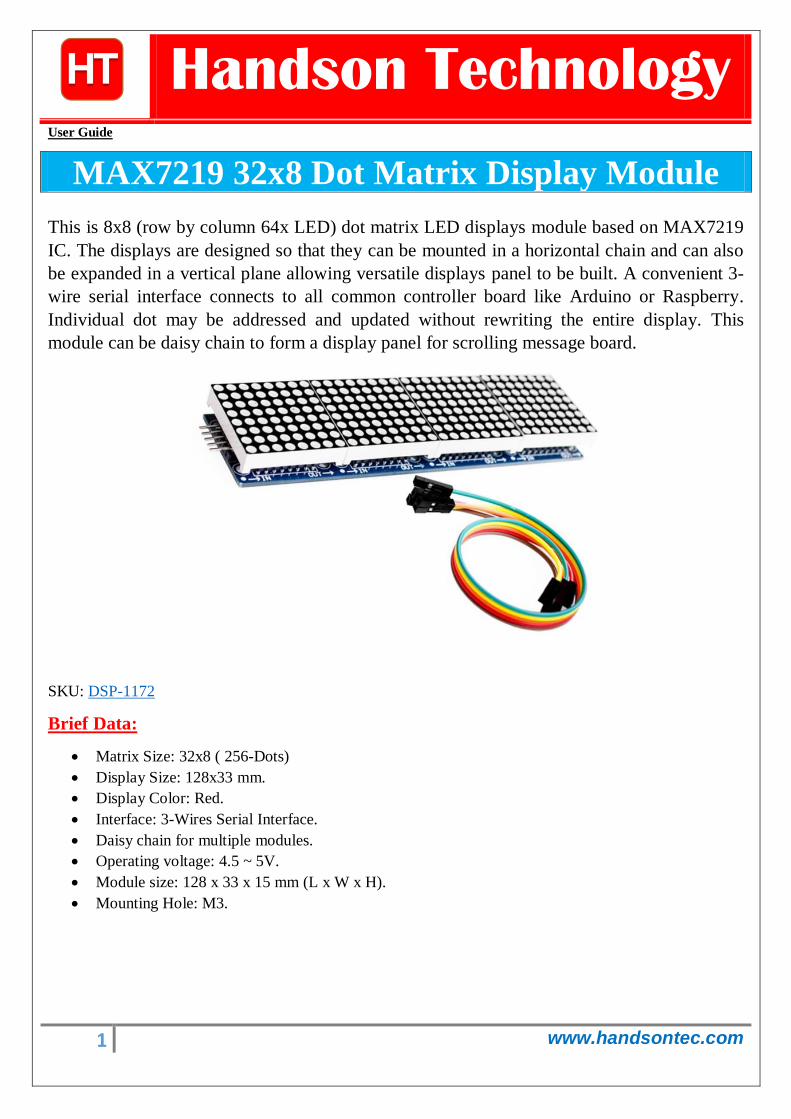
1 www.handsontec.com
Handson Technology
User Guide
MAX7219 32x8 Dot Matrix Display Module
This is 8x8 (row by column 64x LED) dot matrix LED displays module based on MAX7219
IC. The displays are designed so that they can be mounted in a horizontal chain and can also
be expanded in a vertical plane allowing versatile displays panel to be built. A convenient 3-
wire serial interface connects to all common controller board like Arduino or Raspberry.
Individual dot may be addressed and updated without rewriting the entire display. This
module can be daisy chain to form a display panel for scrolling message board.
SKU: DSP-1172
Brief Data:
Matrix Size: 32x8 ( 256-Dots)
Display Size: 128x33 mm.
Display Color: Red.
Interface: 3-Wires Serial Interface.
Daisy chain for multiple modules.
Operating voltage: 4.5 ~ 5V.
Module size: 128 x 33 x 15 mm (L x W x H).
Mounting Hole: M3.

38 Everyday Practical Electronics, August 2018
Lithium-ion (Li-ion) and lithium-ion polymer (LiPo) cells and batteries
are rapidly overtaking all earlier kinds of rechargeable energy storage. They’re now being used in just about all mobile and cordless phones, in USB Power Bank devices used to recharge them, in laptop and tablet PCs and in many portable power tools.
Not only that, but it now looks like Li-ion/LiPo batteries are the preferred power source in the most successful current generation of electric cars, as well as providing some small-scale grid storage.
So it’s not surprising that Li-ion/LiPo charging modules have now be-come readily available on popular internet venues like eBay and AliEx-press, and we will be looking at three examples in this article.
Basic charger modulesProbably the most common charger modules you’ll find on the web are those based on the TP4056 charge con-troller chip, like the one shown oppo-site in the photo at lower right. These modules are quite tiny, measuring only 26 × 20mm and they’re currently available for just a few pounds each, even in small quantities.
There are a few minor variations, but most are very similar to the one pictured; and they are all slight vari-ations of the circuit shown in Fig.1. Some are fitted with a micro-USB type B socket on the input side, while oth-ers have the slightly larger and more rugged mini-USB type B socket. You might choose this type since micro-B sockets can be a bit fragile and can even part from the module PCB when you’re removing the USB cable.
Having said that, micro-B cables are very common and cheap because they are used to charge most modern smart-phones, so that’s a fairly strong reason to prefer the micro version, even if it’s a bit more fragile.
As shown in Fig.1, there’s little in one of these modules apart from the TP4056 controller chip itself. Made by Chinese firm Nanjing Top Power ASIC Corp, the TP4056 comes in a compact SOIC-8 package and provides all of the functions of a single-cell Li-ion/LiPo battery charger, powered from a 5V USB-compatible supply.
It follows the standard CC-CV charg-ing protocol, with a maximum current of 1000mA (1A) in CC (constant cur-rent) mode and a maximum voltage of 4.2V (±1.5%) in CV (constant volt-age) mode. Charging is automatically terminated when the charge current falls to 10% of the programmed value.
The charging current in CC mode can be programmed by changing the value of the RPROG resistor connected between pin 2 of the IC and ground. As supplied, the module has a 1.2k� re-sistor fitted, corresponding to a charg-ing current of 1000mA. If you want a lower charging current, you can select a higher value resistor – as shown by the table at upper right in the diagram.
For example, if you replace the re-sistor with one of 2.0k�, the charg-ing current in CC mode will drop to around 580mA. However, that should only be necessary if the cell you’re charging has a capacity of less than 1Ah, which would make it quite small, and even some cells under 1Ah would be OK being charged at 1A; if in doubt, check the manufacturer’s ratings for that cell.
As well as performing all of the charge control functions, the TP4056 also controls two indicator LEDs to signal the charger’s current state. Red LED1 glows brightly during both charging modes (CC and CV) and ceases glowing when charging is ter-minated. Green LED2 only lights when charging is terminated. Both LEDs re-main off if the USB input voltage is too low (<4.0V) or there is no cell or battery connected.
Note that if you want to power the charger from the USB port of your PC or laptop, it would be a good idea to change the value of RPROG to 2.4k� so that the charging current is reduced to around 500mA; this is the maximum that should be drawn from the USB port of a PC (even though many ports will allow you to draw 1A if you try, at least for a short period). But if you are powering the charger from one of the 5V/1A USB plug packs, RPROG can be left at its default value of 1.2k�.
That’s about it for the basic versions of the USB-powered Li-ion/LiPo charger. They’re cheap as chips but they actu-ally do quite a good job of charging single cells and parallel-cell batteries.
Do keep in mind though that the TP4056 is a linear device, utilising an internal P-channel MOSFET to reduce the incoming supply volt-age of say 5.5V down to the charg-ing voltage of the cell, which could be as low as 3V when fully dis-charged. At a 1A charge current, that’s a dissipation of (5.5V – 3V) × 1A = 2.5W which is quite substantial for an SOIC-8 package and it’s likely to get quite hot under this condition (even more so if you run the chip at its maximum input supply rating of 8V).
Li-Ion and LiPo Charger ModulesThese modules are designed to charge Lithium-ion and Lithium-ion polymer cells. One is low-cost and has a simple design, while the other sports an inbuilt DC-DC boost converter to provide a regulated output voltage from the Li-ion/LiPo cell, since its voltage varies as it charges and discharges.
Using Cheap Asian Electronic Modules Part 8: by Jim Rowe

Everyday Practical Electronics, August 2018 39
This won’t cook the chip since it has thermal regulation, which essentially means that it reduces the charging current if it gets too hot. But it does mean that it will take longer to charge the cell if you run into thermal limit-ing and the charging process won’t be terribly efficient. Considering the size and cost of these modules, that really isn’t a problem.
Fancier versionsIn addition to the basic charger mod-ules, there are more elaborate versions available. One of the most popular of these is shown on the next page. It’s made by the firm Elecrow, based in Shenzen, China, and is about four times the size of the basic modules, measuring 68 × 49mm.
The circuit is shown in Fig.2. The actual Li-ion charger section is based around IC2 at the top. This is a Conso-nance CN3065 chip, which functions in much the same way as the TP4056 device used in the basic modules. As before, the CC mode current level is set via the resistor RPROG connected between pin 2 (ISET) and ground, and the default value of 2.0k� for this resis-tor gives a charging current of 900mA.
The CN3065 again follows the standard CC-CV protocol, with mode switching at 4.2V±1% and charging terminated when the current in CV mode drops to 10% of the programmed CC level. An interesting extra feature is that the cell voltage level at which the device switches from CC mode to CV mode can be raised above 4.2V by adding an external resistor between pin 5 (BAT) and pin 8 (FB). This will result in it reaching full charge sooner.
As with the TP4056, the CN3065 provides outputs to drive two LEDs. LED1 lights during charging, while LED2 lights when charging has termi-nated. Incidentally, the CN3065 is in a very tiny (3 × 3mm) DFN-8 leadless SMD package.
Another nice feature of the Elecrow PSB01012B charger is that it provides a choice of two DC inputs. One is via CON2, the mini-USB input socket, while the other is via CON1, a JST 2.0mm socket designated as the input from a solar photovoltaic panel. (A sec-ond JST 2.0 socket [CON3] is used for the Li-ion cell connection.) Schottky diodes D1 and D2 are used to feed the two inputs to IC2, so no input switch-ing is required.
Note that the D– and D+ USB data lines of CON2 are taken through to USB output socket CON4, a standard USB type A socket. That’s because the PSB01012B is not just a charger, but in effect a USB Li-ion power pack as well. It’s also the reason for on-off
switch S1, in series with battery con-nector CON3. But note that S1 will need to be in the ON position for charging to take place.
The other half of the Elecrow PS-B01012B module provides a regulated +5V supply from the varying output of the Li-ion cell. This is the function of the circuitry around IC1, REG1 and IC3, in the lower half of Fig.2.
IC1 is the actual output voltage regulator. This is an Intersil ISL97516 device, described as a high-frequency, high-efficiency step-up (boost) voltage regulator, which operates in a constant frequency PWM mode. It’s in a very small MSOP-8 package.
The ISL97516 operates at a nomi-nal frequency of 620kHz or 1250kHz, selected by connecting pin 7 (FSEL) to ground or pin 6 (VDD). As you can see from Fig.2, in the Elecrow mod-ule it’s programmed for 620kHz. The switching FET inside the device has a maximum current limit of 2.0A and an on-resistance of 200m�. As a result, it’s claimed to deliver over 90% con-version efficiency – quite impressive.
The input voltage range of the ISL97516 is rated at 2.3-5.5V, which is well suited to its application here. The output voltage range is specified as 5-25V. The actual output voltage is determined by the proportion of the output voltage fed back to pin 2 (FB) of the device, via a resistive divider. In the Elecrow module, the divider formed from the 43k� and 15k� resis-tors programs it to give an output of 5V.
Other attractive features of the ISL97516 include sensing of the cur-rent in the switching FET for thermal overload protection and a soft-start feature which allows slowing down of the internal oscillator’s startup by connecting a capacitor from pin 8 (SS) and ground. As you can see in the
Elecrow module, a 27nF capacitor is used for this.
The regulated 5V output from IC1 appears across the 47μF capacitor at the cathode of diode D3 and is then filtered before being fed to pin 1 of the USB output connector CON4.
So that’s the boost converter/regula-tor section. But what about the rest of the module’s circuit, involving REG1 and two op amps in IC3? This addi-tional circuitry is basically to monitor the Li-ion/LiPo cell voltage, and signal if it drops below a safe level. REG1 is a Micrel MIC5205-2.5 low noise LDO regulator, used to derive a 2.5V±1% reference from the cell voltage.
This is fed to op amps IC3a and IC3b, which are used as comparators. The second input of each ‘comparator’ is fed with a proportion (0.6875) of the cell voltage, derived by the resis-tive divider formed by the 150k� and 330k� resistors.
Fig.1: circuit diagram for the basic TP4056 module. Note that many modules of this type will differ slightly from this circuit diagram.
This TP4056 module shown uses a micro-USB[2] connector, but there are some that use mini-USB[1].
Reproduced by arrangement with SILICON CHIP
magazine 2018.www.siliconchip.com.au

Everyday Practical Electronics, August 2018
This voltage is fed to the positive input of the IC3a comparator and the negative input of the IC3b comparator. As a result, whenever the divided-down cell voltage is above +2.5V, IC3a turns on LED3 to indicate that the cell voltage is OK.
By contrast, if the divided-down cell voltage falls below +2.5V, IC3a turns off LED3 and IC3b turns on LED4 to indicate that the cell is nearing the limit of safe discharging. This oc-curs at 2.5V ÷ 0.6875 = 3.64V, a little above the minimum recommended discharge voltage to achieve the best cell lifespan.
So the Elecrow charger module with its inbuilt +5V output regulator provides significantly more capabilities than the basic modules. It actually provides all of the functions needed for making your own USB Power Bank, using a Li-ion or LiPo cell/battery of your own choosing. Plus, it has the ability to charge your Li-ion/LiPo cell from a solar panel.
So although it will cost you signifi-cantly more than one of the basic mod-ules, it’s still good value for money.
Trying them outI tried a couple of the basic TP4056-based charger modules with both a single 18650 Li-ion cell and a battery of two parallel-connected 18650 cells.
The chargers did everything that could be expected from them, charging the cells repeatedly with no problems – apart from the micro-B USB input socket breaking away from one of the modules when I tried to unplug the cable from the USB plug pack. Hence my suggestion to prefer the mini-USB socket version.
I also tried out one of the fancier Elecrow PSB01012B modules, al-though this did involve getting hold of some cables with the very small JST 2.0 connectors (for the Li-ion cell cables, to connect to CON3).
As a charger, this one worked just as well as the basic modules. But where it really shone was on the output side, being able to provide a regulated +5V output (or reasonably close to it; about 4.85V) for the USB device connected to CON4’s output, even for a load drawing 500mA and with a partly discharged Li-ion cell with a terminal voltage down to about 3.8V.
In fact, it kept providing this regulat-ed output voltage even when the Li-ion cell dropped down below 3.0V, after about 40 minutes. Quite impressive! (But not recommended if you want your cell to last a long time.)
It might seem to be nit-picking, but I’d like to have seen the Elecrow module’s regulated USB output closer
to the nominal +5V under load than 4.85V. If you calculate the expected output voltage for IC1, you get 1.294V × (43k� ÷ 15k� + 1) = 5.0V, so this is likely a component tolerance issue that requires trimming.
This could be achieved by measur-ing the actual output voltage and then paralleling the 15k� resistor with a higher value SMD resistor, by solder-ing it on top. For example, in my case, the output needs to be raised by (5.0V – 4.85V) ÷ 4.85V = 3.1%, so a resistor of 15k� ÷ 0.031 = 483,870� or say 470k��should do the trick.
I also think that ALARM LED4 should ideally be a red one, not an-other green one as it is at present. It’s right next to green LED3, making it difficult to see when LED4 has lit up. You could fix this by de-soldering LED4 and fitting a red LED in its place.
My only other complaint about the Elecrow module was that the very small slider switch used for power switch S1 was very flimsy. Perhaps it had been damaged in transit, but at one point the tiny actuator almost came out of the switch body – not a good sign.
One more point – it would be a good idea if the unit could be set up to au-tomatically switch off the output if the cell voltage drops too low, to prevent damage from over-discharge. Some
Fig.2: circuit diagram for the Elecrow PSB01012B charger module which utilises a CN3065 IC instead of the TP4056 detailed earlier (the CN3065 is functionally identical to the TP4056).
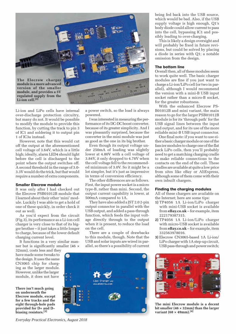
Everyday Practical Electronics, August 2018
Li-ion and LiPo cells have internal over-discharge protection circuitry, but many do not. It would be possible to modify the module to provide this function, by cutting the track to pin 3 of IC1 and soldering it to output pin 1 of IC3a instead.
However, note that this would cut off the output at the aforementioned cell voltage of 3.64V, which is a little high; ideally, alarm LED4 should light before the cell is discharged to the point where the output switches off. A second threshold in the range of 3.0-3.3V would do the trick, but that would require a number of extra components.
Smaller Elecrow moduleIt was only after I had checked out the Elecrow PSB01012B module that I learned about their other ‘mini’ mod-ule. Luckily I was able to get a hold of one of these quickly, in order check it out as well.
As you’d expect from the circuit (Fig.3), its performance as a Li-ion cell charger is very close to that of its big-ger brother – it just takes a little longer to charge, because of the lower default charging current level.
It functions in a very similar man-ner but is significantly smaller (46 × 32mm), costs less and they have made some tweaks to the design. It uses the same CN3065 chip for charg-ing as the larger module. However, unlike the larger module, it does not have
a power switch, so the load is always powered.
I was interested in measuring the per-formance of its DC-DC boost converter, because of its greater simplicity. And I was pleasantly surprised, because the converter in the mini module was just as good as the one in its big brother.
Even though its output voltage un-der 250mA of loading was slightly lower at 4.80V with a cell voltage of 3.84V, it only dropped to 4.78V when the cell voltage fell to the recommend-ed minimum of 3.0V. So it might be a lot simpler, but it’s just as impressive in terms of conversion efficiency.
The other differences are as follows. First, the input power socket is a micro type-B, rather than mini. Second, the output current capability is lower, at 500mA compared to 1A.
They have also added a JST 2.0 2-pin output connector in parallel with the USB output, and added a pass-through function, which feeds the input volt-age directly through to the output when it is present, to reduce the load on the cell.
There are a couple of drawbacks to this module, though. Note that the USB and solar inputs are wired in par-allel, so there’s a possibility of current
being fed back into the USB source, which would be bad. Also, if the USB supply voltage is high enough, Q1’s body diode could allow current to pass into the cell, bypassing IC1 and pos-sibly leading to over-charging.
This is likely a design oversight and will probably be fixed in future revi-sions, but could be solved by placing a diode in series with Q1; a notable omission from the design.
The bottom lineOverall then, all of these modules seem to work quite well. The basic charger modules are fine if you just want to charge a Li-ion/LiPo cell (or two in par-allel), although I would recommend the version with a mini-B USB input socket rather than a micro-B socket, for the greater robustness.
With the enhanced Elecrow PS-B01012B and mini variant, the main reason to go for the larger PSB01012B module is for its ‘through path’ for the USB signal lines between the input and output, and for its use of the more reliable mini-B USB input connector.
One final note: if you want to use ei-ther a basic charger module or one of the fancier modules to charge one of the flat pack LiPo cells, then you’ll probably need to get a matching charging cradle to make reliable connections to the contacts on the end of the cell. These cradles are available at quite a low price from sites like eBay or AliExpress, although some of them come with their own inbuilt chargers.
Finding the charging modulesAll of these chargers are available on the Internet; here are some tips:1) TP4056 1A Li-ion/LiPo charger
with mini-USB socket is available from eBay.co.uk – for example, item 222179387315.
2) TP4056 1A Li-ion/LiPo charger with micro-USB socket is available from eBay.co.uk – for example, item 332563978016.
3) Elecrow CN3065-based 1A Li-ion/LiPo charger with 1A step-up circuit, USB pass-through and power switch;
The Elecrow charger module is a more advanced version of the smaller module, and provides a 5V regulated supply from the Li-ion cell.[3]
There isn’t much going on underneath the Elecrow module, except for a few tracks and the eight through-hole pads provided for D+ and D– biasing resistors.[3]
The mini Elecrow module is a decent bit smaller (46 × 32mm) than the larger variant (68 × 49mm).[4]
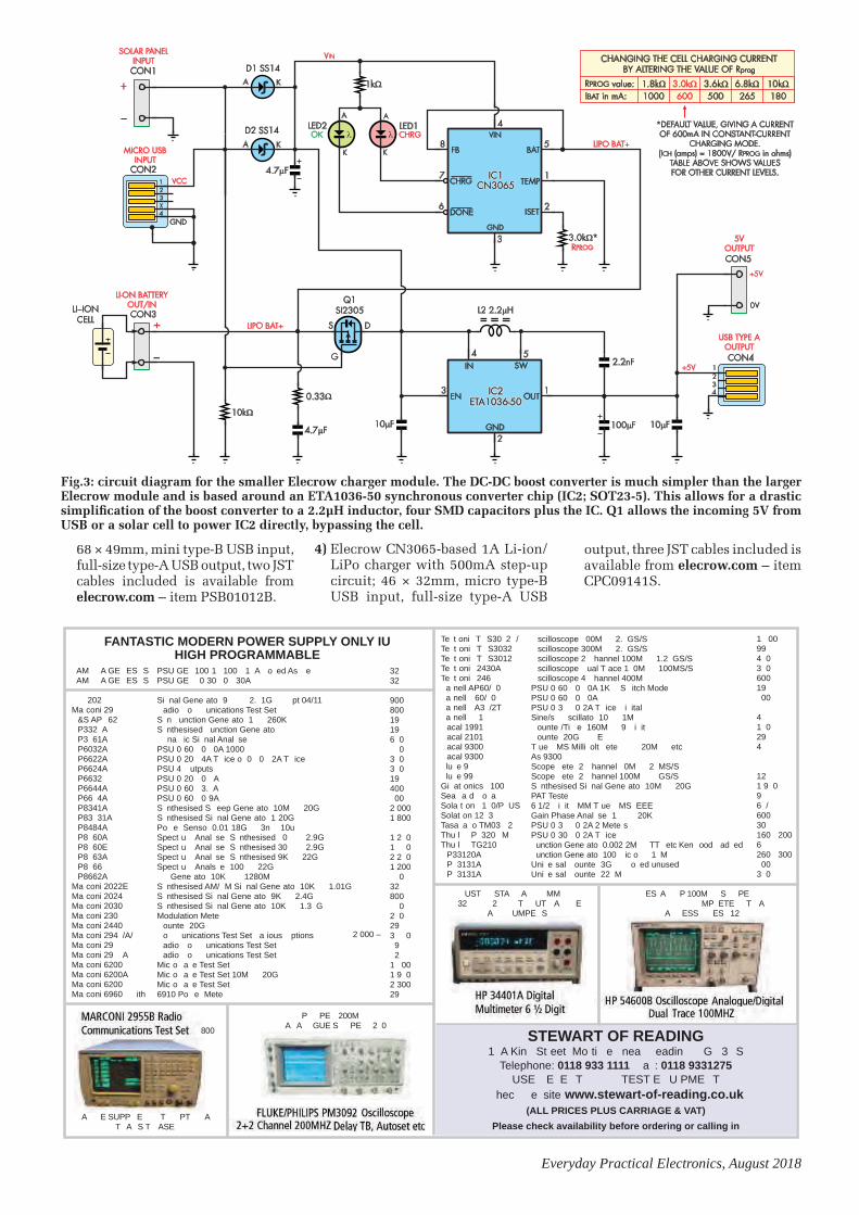
Everyday Practical Electronics, August 2018
68 × 49mm, mini type-B USB input, full-size type-A USB output, two JST cables included is available from elecrow.com – item PSB01012B.
4) Elecrow CN3065-based 1A Li-ion/LiPo charger with 500mA step-up circuit; 46 × 32mm, micro type-B USB input, full-size type-A USB
output, three JST cables included is available from elecrow.com – item CPC09141S.
Fig.3: circuit diagram for the smaller Elecrow charger module. The DC-DC boost converter is much simpler than the larger Elecrow module and is based around an ETA1036-50 synchronous converter chip (IC2; SOT23-5). This allows for a drastic simplification of the boost converter to a 2.2μH inductor, four SMD capacitors plus the IC. Q1 allows the incoming 5V from USB or a solar cell to power IC2 directly, bypassing the cell.
Te t oni T S30 2 /Te t oni T S3032Te t oni T S3012Te t oni 2430ATe t oni 246
a nell AP60/ 0a nell 60/ 0a nell A3 /2Ta nell 1acal 1991acal 2101acal 9300acal 9300lu e 9lu e 99
Gi at onics 100Sea a d o aSola t on 1 0/P USSolat on 12 3Tasa a o TM03 2Thu l P 320 MThu l TG210
P33120AP 3131AP 3131A
scilloscope 00M 2. GS/Sscilloscope 300M 2. GS/Sscilloscope 2 hannel 100M 1.2 GS/Sscilloscope ual T ace 1 0M 100MS/Sscilloscope 4 hannel 400M
PSU 0 60 0 0A 1K S itch ModePSU 0 60 0 0APSU 0 3 0 2A T ice i italSine/s scillato 10 1M
ounte /Ti e 160M 9 i itounte 20G E
T ue MS Milli olt ete 20M etcAs 9300Scope ete 2 hannel 0M 2 MS/SScope ete 2 hannel 100M GS/SS nthesised Si nal Gene ato 10M 20GPAT Teste6 1/2 i it MM T ue MS EEEGain Phase Anal se 1 20KPSU 0 3 0 2A 2 Mete sPSU 0 30 0 2A T ice
unction Gene ato 0.002 2M TT etc Ken ood ad edunction Gene ato 100 ic o 1 M
Uni e sal ounte 3G o ed unusedUni e sal ounte 22 M
1 00994 03 06001900
41 0294
121 9 096 /60030160 2006260 30000
3 0
STEWART OF READING1 A Kin St eet Mo ti e nea eadin G 3 S
Telephone: 0118 933 1111 a : 0118 9331275USE E E T TEST E U PME T
hec e site www.stewart-of-reading.co.uk(ALL PRICES PLUS CARRIAGE & VAT)
Please check availability before ordering or calling in
AM A GE ES SAM A GE ES S
202Ma coni 29
&S AP 62P332 AP3 61AP6032AP6622AP6624AP6632P6644AP66 4AP8341AP83 31AP8484AP8 60AP8 60EP8 63AP8 66P8662A
Ma coni 2022EMa coni 2024Ma coni 2030Ma coni 230Ma coni 2440Ma coni 294 /A/Ma coni 29Ma coni 29 AMa coni 6200Ma coni 6200AMa coni 6200Ma coni 6960 ith
PSU GE 100 1 100 1 A o ed As ePSU GE 0 30 0 30A
Si nal Gene ato 9 2. 1G pt 04/11adio o unications Test Set
S n unction Gene ato 1 260KS nthesised unction Gene ato
na ic Si nal Anal sePSU 0 60 0 0A 1000PSU 0 20 4A T ice o 0 0 2A T icePSU 4 utputs PSU 0 20 0 APSU 0 60 3. APSU 0 60 0 9AS nthesised S eep Gene ato 10M 20GS nthesised Si nal Gene ato 1 20GPo e Senso 0.01 18G 3n 10uSpect u Anal se S nthesised 0 2.9GSpect u Anal se S nthesised 30 2.9GSpect u Anal se S nthesised 9K 22GSpect u Anals e 100 22G
Gene ato 10K 1280MS nthesised AM/ M Si nal Gene ato 10K 1.01GS nthesised Si nal Gene ato 9K 2.4GS nthesised Si nal Gene ato 10K 1.3 GModulation Mete
ounte 20Go unications Test Set a ious ptionsadio o unications Test Setadio o unications Test Set
Mic o a e Test SetMic o a e Test Set 10M 20GMic o a e Test Set 6910 Po e Mete
3232
90080019196 0
03 03 01940000
2 0001 800
1 2 01 02 2 01 200
032800
02 0293 092
1 001 9 02 30029
2 000 –
FANTASTIC MODERN POWER SUPPLY ONLY IU HIGH PROGRAMMABLE
A E SUPP E T PT A T A S T ASE
P PE 200M A A GUE S PE 2 0
UST STA A MM 32 2 T UT A E
A UMPE S
ES A P 100M S PE MP ETE T A
A ESS ES 12
800

1 www.handsontec.com
Handson Technology
Datasheet
18650 Lithium Battery Charger Module with Protection
5V microUSB 1-Amp 18650 Lithium Battery Charging Board Charger Module+Protection.
This versatile charger module is based on TP4056 IC, a constant-current/constant-voltage
linear charger chip for single cell lithium-ion batteries. This charger module can be powered
from USB or wall adapter. The features include current monitor, under voltage lockout,
automatic recharge and two status LED to indicate charge termination and the presence of an
input voltage.
SKU: MDU-1000
Brief Data:
High Quality double side PCB design.
Charge mode - Linear charging.
Charges Single Cell Li-Ion Batteries Directly from USB Port.
Charging Current: Preset to 1A max. (with R3=1.2K )
C/10 Charge Termination.
Preset 4.2V Charge Voltage with 1.5% Accuracy.
Input voltage: 4.5V-5.5V.
Full charge voltage: 4.2V.
Led indicator- red is charging, blue is full charged.
Power Input interface: micro USB and terminal pin.
Work temperature: -10℃ to +85℃.
Built-in protection circuit.
Size- small to 25x19x1mm.
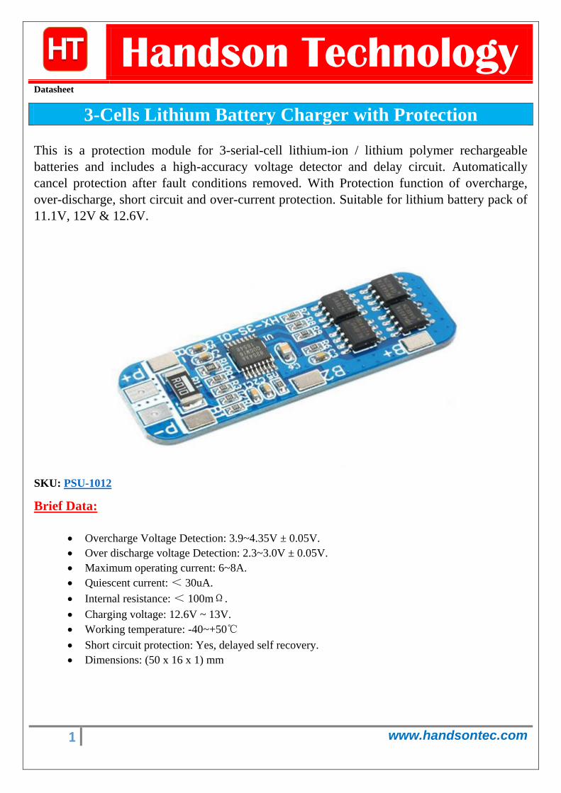
1 www.handsontec.com
Handson Technology
Datasheet
3-Cells Lithium Battery Charger with Protection
This is a protection module for 3-serial-cell lithium-ion / lithium polymer rechargeable
batteries and includes a high-accuracy voltage detector and delay circuit. Automatically
cancel protection after fault conditions removed. With Protection function of overcharge,
over-discharge, short circuit and over-current protection. Suitable for lithium battery pack of
11.1V, 12V & 12.6V.
SKU: PSU-1012
Brief Data:
Overcharge Voltage Detection: 3.9~4.35V ± 0.05V.
Over discharge voltage Detection: 2.3~3.0V ± 0.05V.
Maximum operating current: 6~8A.
Quiescent current: < 30uA.
Internal resistance: < 100mΩ.
Charging voltage: 12.6V ~ 13V.
Working temperature: -40~+50℃
Short circuit protection: Yes, delayed self recovery.
Dimensions: (50 x 16 x 1) mm

4 www.handsontec.com
Handsontec.com
HandsOn Technology provides a multimedia and interactive platform for
everyone interested in electronics. From beginner to diehard, from student
to lecturer. Information, education, inspiration and entertainment. Analog
and digital, practical and theoretical; software and hardware.
HandsOn Technology support Open Source Hardware (OSHW) Development Platform.
Learn : Design : Share
www.handsontec.com

5 www.handsontec.com
The Face behind our product quality…
In a world of constant change and continuous technological development, a new or replacement
product is never far away – and they all need to be tested.
Many vendors simply import and sell wihtout checks and this cannot be the ultimate interests of
anyone, particularly the customer. Every part sell on Handsotec is fully tested. So when buying from
Handsontec products range, you can be confident you’re getting outstanding quality and value.
We keep adding the new parts so that you can get rolling on your next project.
Breakout Boards & Modules
Connectors Electro-Mechanical Parts
Engineering Material
Mechanical Hardware
P Electronics Components
Power Supply Arduino Board & Shield
Tools & Accessory