the photophysics of nano carbons - kitp online conferences,...
TRANSCRIPT
The Photophysics
of Nano Carbons
Kavli Institute, UC Santa Barbara
January 9, 2012
M. S. Dresselhaus, MIT
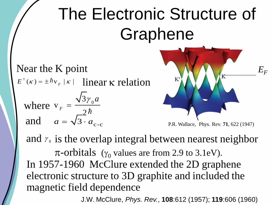
c-c3a a P.R. Wallace, Phys. Rev. 71, 622 (1947)
In 1957-1960 McClure extended the 2D graphene electronic structure to 3D graphite and included the magnetic field dependence
Near the K point
is the overlap integral between nearest neighbor
-orbitals (0 values are from 2.9 to 3.1eV).
0
( ) v | |F
E
linear relation
03
v2
F
a
and
and
EF
where
J.W. McClure, Phys. Rev., 108:612 (1957); 119:606 (1960)
The Electronic Structure of
Graphene
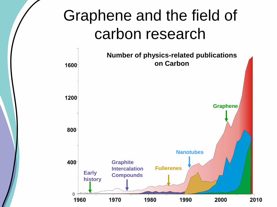
Graphene and the field of
carbon research
Number of physics-related publications
on Carbon
Early
history
Fullerenes
Nanotubes
Graphene
Graphite
Intercalation
Compounds
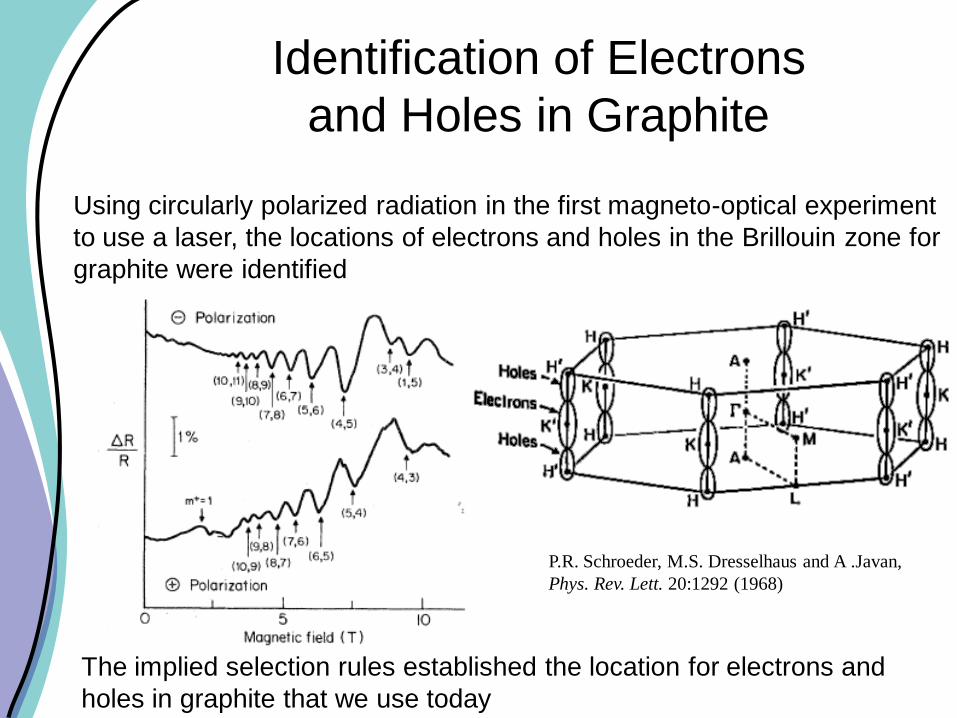
Identification of Electrons
and Holes in Graphite
The implied selection rules established the location for electrons and
holes in graphite that we use today
Using circularly polarized radiation in the first magneto-optical experiment
to use a laser, the locations of electrons and holes in the Brillouin zone for
graphite were identified
P.R. Schroeder, M.S. Dresselhaus and A .Javan,
Phys. Rev. Lett. 20:1292 (1968)

• Observation of superconductivity in stage
1 graphite intercalation compounds (C8K)
My entry into the Nanoworld
(1973)
Hannay et al, Phys. Rev. Lett. 14:225 (1965)
C8K
aroused much interest in nanocarbonssince neither potassium nor carbon is superconducting
• Intercalation compounds allowed early studies to be made of individual or few graphene layers in the environment of the intercalant species.
• Many properties were studied 1973-1990.
M.S. Dresselhaus and G. Dresselhaus, Advances in Physics 30:139-326 (1981)
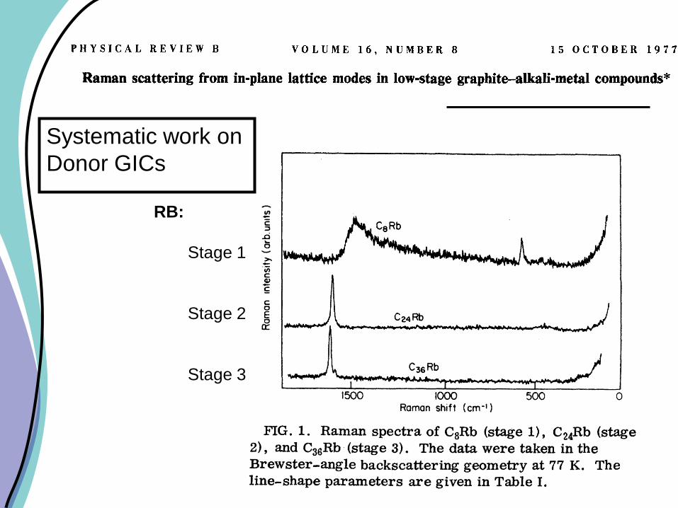
Systematic work on
Donor GICs
RB:
Stage 1
Stage 2
Stage 3

Acceptor GIC
with bromine

Discovery of Fullerenes
E.A. Rohlfing, D.M. Cox, and A.Kaldor. J. Chem. Phys., 81:332 (1984)
• The Laser ablation process used to
make liquid carbon caused the
emission of large carbon clusters
(like C100) rather than C2 and C3 with
relatively low laser energy input
• A trip was made to Exxon Research
Lab to discuss results.
• Soon (1984) Exxon published the
famous result for the mass spectra.
In 1985 fullerenes were discovered
by Kroto, Smalley, and Curl
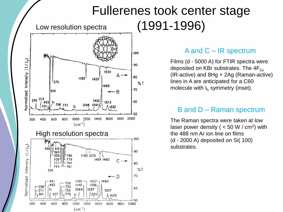
Fullerenes took center stage
(1991-1996)Low resolution spectra
High resolution spectra
The Raman spectra were taken at low
laser power density ( < 50 W / cm2) with
the 488 nm Ar ion line on films
(d - 2000 A) deposited on Si( 100)
substrates.
B and D – Raman spectrum
Films (d - 5000 A) for FTIR spectra were
deposited on KBr substrates. The 4F1u
(IR-active) and 8Hg + 2Ag (Raman-active)
lines in A are anticipated for a C60
molecule with Ih symmetry (inset).
A and C – IR spectrum

A.M. Rao, P.C. Eklund, R.E. Smalley, M.S. Dresselhaus, et al., Science 275:187(1997)
Resonance enhancement of
Raman signal enabled
detection of SWNTs in bundlesSingle nanotube Raman spectroscopy
was observed
Resonance Raman Spectroscopy on
single wall carbon nanotubes (SWNTs)
Sem
iconductin
gM
etallic
A. Jorio et al., Phys. Rev. Lett. 86:1118 (2001)
Elaser
= 0.94eV
= 1.17eV
= 1.58eV
= 1.92eV
= 2.41eV
Single nanotube spectroscopy has since been demonstrated in photoluminescence and in Rayleigh scattering experiments.
From the spectrum of a nanotube its
geometry and properties can be determined
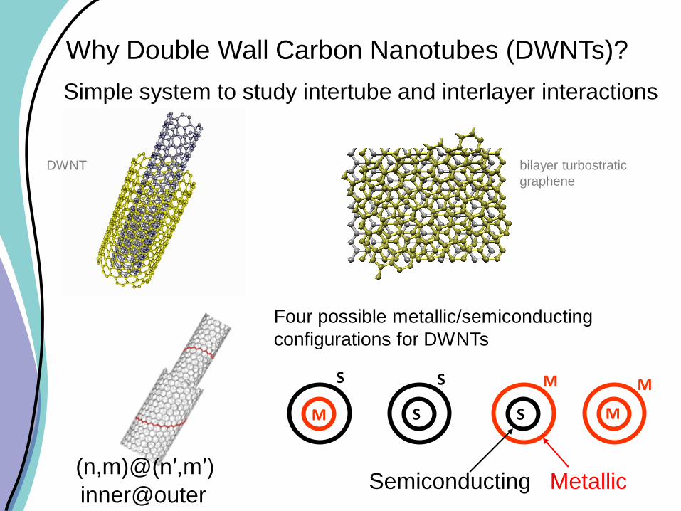
Why Double Wall Carbon Nanotubes (DWNTs)?
Four possible metallic/semiconducting
configurations for DWNTs
MetallicSemiconducting
S
M
S
S M
MM
S
(n,m)@(n′,m′)
inner@outer
Simple system to study intertube and interlayer interactions
bilayer turbostratic
graphene
DWNT
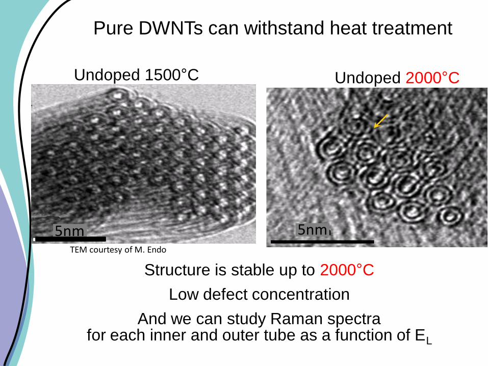
Pure DWNTs can withstand heat treatment
TEM courtesy of M. Endo
5nm 5nm
Undoped 1500°C Undoped 2000°C
Structure is stable up to 2000°C
Low defect concentration
And we can study Raman spectra for each inner and outer tube as a function of EL
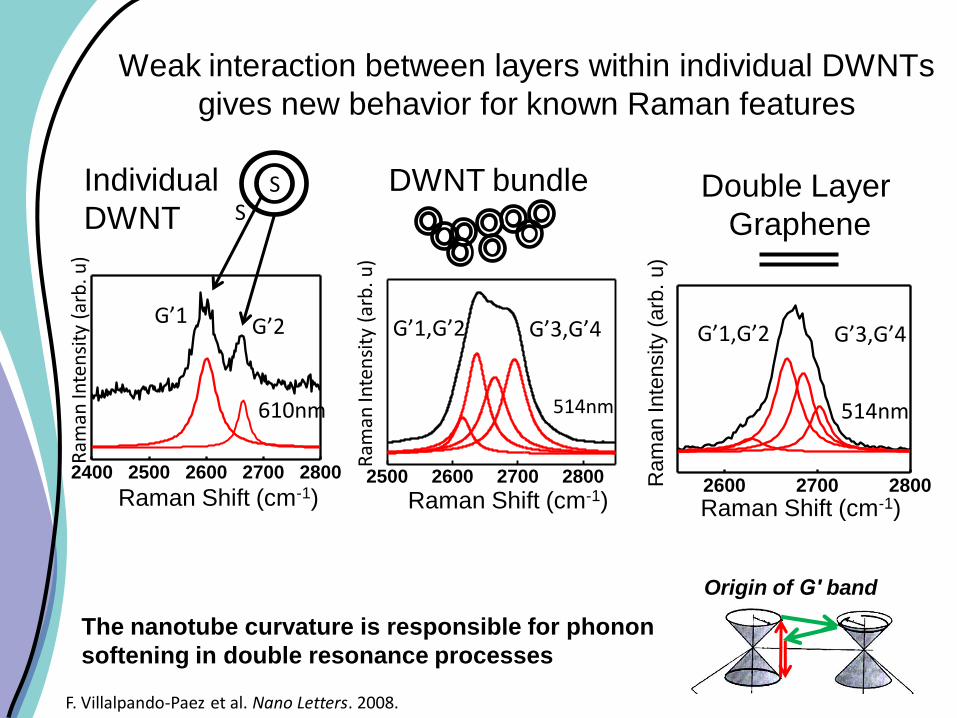
F. Villalpando-Paez et al. Nano Letters. 2008.
2600 2700 2800
G’1,G’2
514nm
Double Layer
Graphene
Raman Shift (cm-1)
G’3,G’4
Ram
an Inte
nsity (
arb
. u)
2500 2600 2700 2800
514nm
G’3,G’4
DWNT bundle
Raman Shift (cm-1)
G’1,G’2
Ram
an In
ten
sity
(ar
b. u
)
2400 2500 2600 2700 2800
610nm
SS
G’1 G’2
Individual
DWNT
Raman Shift (cm-1)
Ram
an In
ten
sity
(ar
b. u
)Weak interaction between layers within individual DWNTs
gives new behavior for known Raman features
The nanotube curvature is responsible for phonon
softening in double resonance processes
Origin of G′ band

Graphene and the field of
carbon research
Number of physics-related publications
on Carbon
Early
history
Fullerenes
Nanotubes
Graphene
Graphite
Intercalation
Compounds

Thinnest material sheet
imaginable…yet the strongest!
(5 times stronger than steel and
much lighter!)
Graphene is a zero band gap
semiconductor: it conducts as well
as the best metals, yet its electrical
properties can be modulated (it can
be switched “ON” and “OFF”)
Very high current densities (equivalent to ~109 A/cm2)
Superb heat conductor (~5∙103 W/m∙K)
High mobility (100000 cm2/Vs @RT)
Ballistic conduction for hundreds of nm

Bipolar materials (electrons and holes)
Low energy behavior described by
Dirac equation
Truly 2D: pure surface with no bulk!
Band structure can be modified by
application of electromagnetic fields
Band structure of graphene structures
depends on geometry (stacking, size,
and atomic structure)
Interesting electron spin dynamics
(weak spin orbit, nearly absent
hyperfine interaction, etc…)

Mono-layer
Bi-layer
Raman Spectrum for Graphene
Ferrari et al., 2006
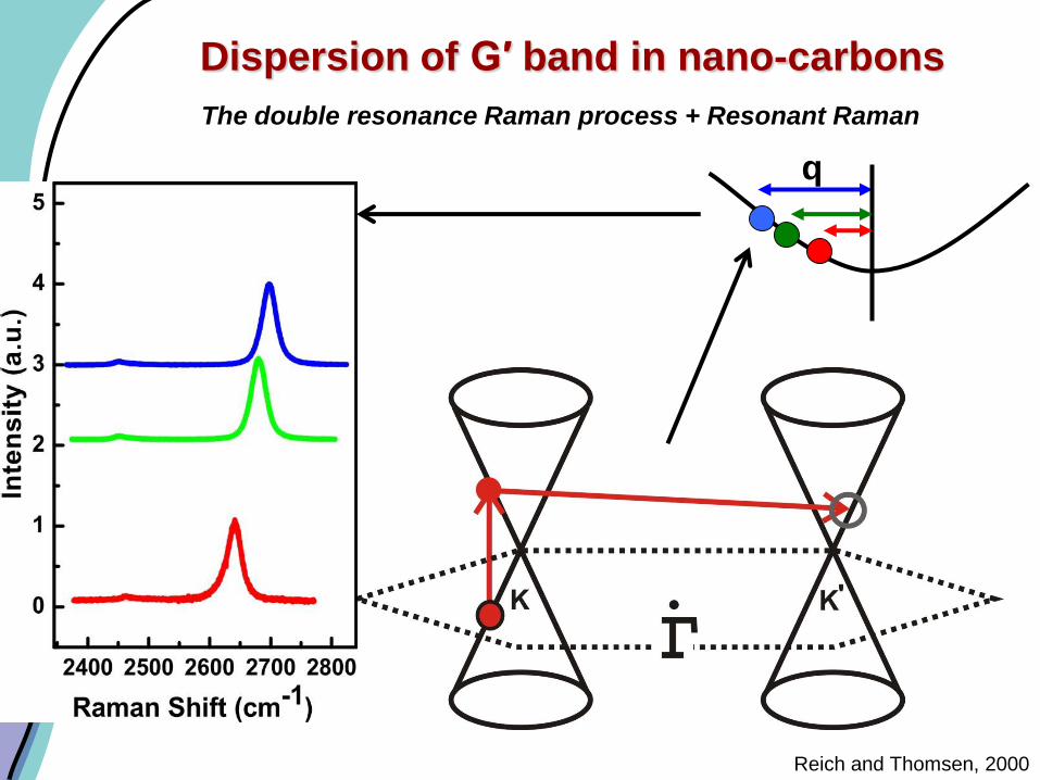
Dispersion of G′ band in nano-carbons
The double resonance Raman process + Resonant Raman
q
Reich and Thomsen, 2000
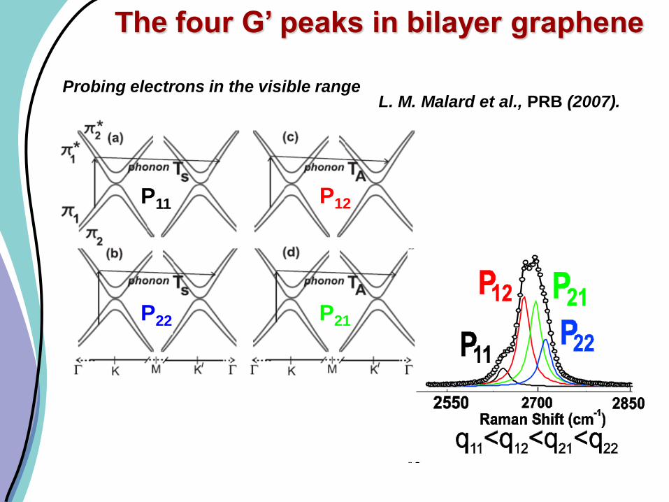
The four G’ peaks in bilayer graphene
Probing electrons in the visible rangeL. M. Malard et al., PRB (2007).
P11
P22
P12
P21

Dispersion of the four G′ peaks
in bilayer graphene
P11
P22
P21
P12
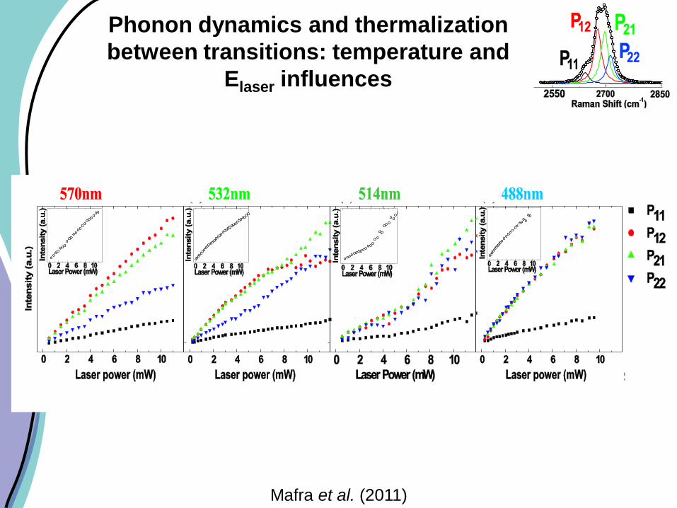
Phonon dynamics and thermalization
between transitions: temperature and
Elaser influences
Mafra et al. (2011)
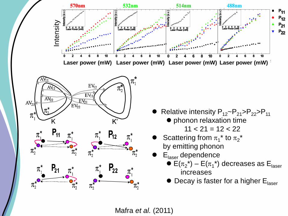
Relative intensity P12~P21>P22>P11
phonon relaxation time
11 < 21 = 12 < 22
Scattering from 1* to 2*
by emitting phonon
Elaser dependence
E(2*) – E(1*) decreases as Elaser
increases
Decay is faster for a higher Elaser
Mafra et al. (2011)
Laser power (mW) Laser power (mW) Laser power (mW) Laser power (mW)In
ten
sity

Phonon self-energy corrections to non-zero wavevector
phonon modes in single-layer graphene
(Self-consistently determined)
DC – voltage source
100 X
532 nm
Spectrometer
Our contacts:
Au (80nm)
+ Cr (5nm) 1500 2000 2500
G'-band
G*-band
Raman shift (cm-1)
G-band
Exfoliated graphene
How do we obtain this information?,
Experiment to vary
Fermi level

What is known so far...
-100 -50 0 50 100
1582
1583
1584
1585
EF (eV)
G (
cm
-1)
VG (V)
0.340.240-0.24
-0.34
-100 -50 0 50 100
10.5
12.0
13.5
G
(c
m-1)
VG (V)
EF (eV)
0.340.240-0.24 -0.34
Experiment:(Phys. Rev. Lett. 101:136804 (2008))
-0.2 0.0 0.2
0.0
0.5
1.0
|EF| ~ |E
ph /2|
|EF| >> |E
ph /2|
Re
[
(q,
EF )
]
EF (eV)
-0.2 0.0 0.2
0.0
0.5
1.010K
Im [
(q,
EF )
]
EF (eV)
300K
Theory:(Rev. Mod. Phys. 81:109 (2009))
1500 2000 2500
G'-band
G*-band
Raman shift (cm-1)
G-band
Results for
G-band variation
with Fermi level
G-band results

What is new? For combination and overtone modes...
Theory:
For G(K)-point q≠0 and K-point q=0 phonons:
Frequency Line width
Araujo et al. 2011
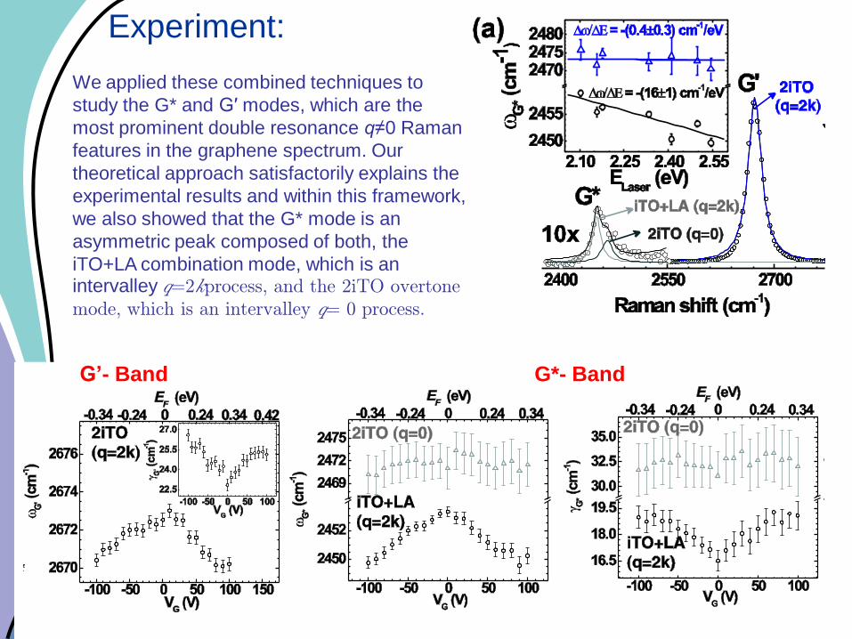
Experiment:
We applied these combined techniques to
study the G* and G′ modes, which are the
most prominent double resonance q≠0 Raman
features in the graphene spectrum. Our
theoretical approach satisfactorily explains the
experimental results and within this framework,
we also showed that the G* mode is an
asymmetric peak composed of both, the
iTO+LA combination mode, which is an intervalley q=2k process, and the 2iTO overtone
mode, which is an intervalley q = 0 process.
G’- Band G*- Band

-100 -50 0 50 100
1582
1583
1584
1585
EF (eV)
G (
cm
-1)
VG (V)
0.340.240-0.24
-0.34
-100 -50 0 50 100
10.5
12.0
13.5
G
(c
m-1)
VG (V)
EF (eV)
0.340.240-0.24 -0.34
1500 2000 2500
G'-band
G*-band
Raman shift (cm-1)
G-band
G′ – band G* – band
G – band
Conclusions (The take-home messages):
Thank you
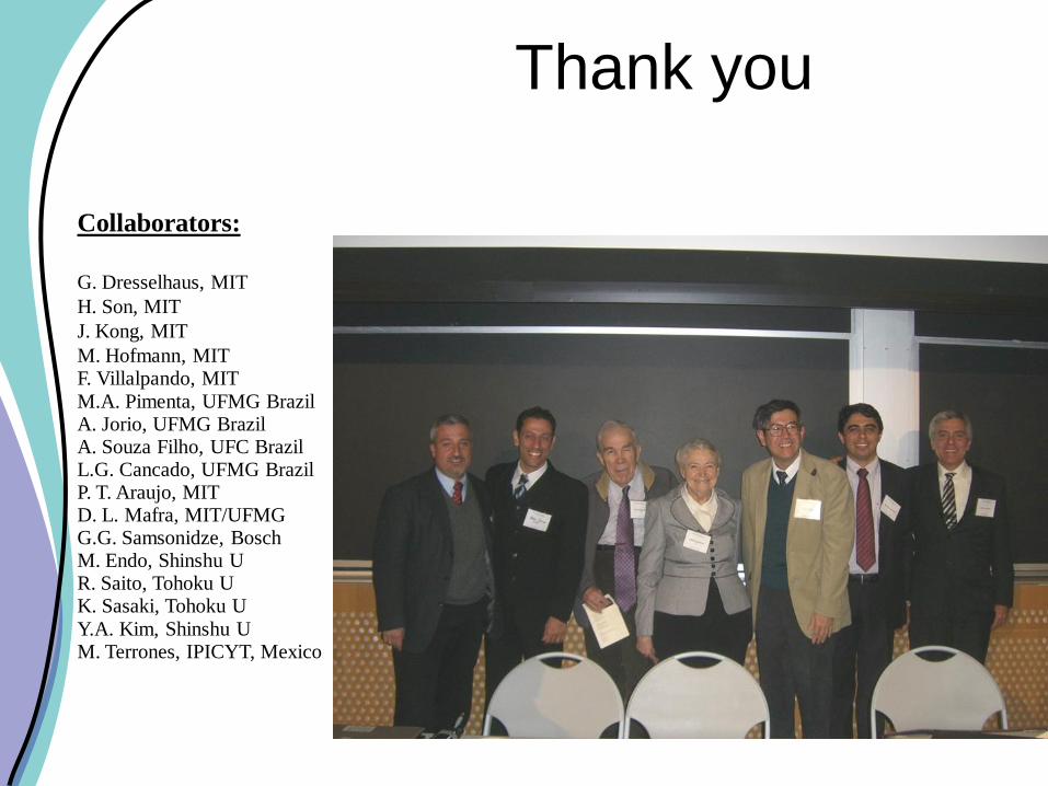
Collaborators:
G. Dresselhaus, MIT
H. Son, MIT
J. Kong, MIT
M. Hofmann, MITF. Villalpando, MITM.A. Pimenta, UFMG BrazilA. Jorio, UFMG BrazilA. Souza Filho, UFC BrazilL.G. Cancado, UFMG BrazilP. T. Araujo, MITD. L. Mafra, MIT/UFMG G.G. Samsonidze, BoschM. Endo, Shinshu UR. Saito, Tohoku UK. Sasaki, Tohoku UY.A. Kim, Shinshu UM. Terrones, IPICYT, Mexico
The End