the readout chip for the xfel dssc detector: design and test
TRANSCRIPT

FEE 2018
1
The readout chip for the XFEL DSSC Detector:
design and test
Pradeep Kalavakuru, DESY
for the DSSC ASIC design groups
C. Fiorini3, P. Fischer2, K. Hansen1, F. Erdinger2, M. Kirchgessner2,M. Manghisoni4, M. Porro5, C. Reckleben1, J. Soldat2
(DESY1 , Heidelberg Univ.2, Politecnico di Milano3,
Univ. de Bergamo4, European XFEL GmbH 5)
FEE 2018
2
Outline
● Project Status
● Overview
● Characterization
ADC
Front-end
● Measurements with Sensor
Small format ASICS - X-ray sources
Focal Plane Module (FPM) - LED
● Summary

FEE 2018
3
DSSC Project Status - mini-SDD & DEPFET Cameras
Two camera types
active: DEPFET with gain compression
passive: miniaturized Silicon-Drift Cells / linear gain
mini-SDD
Mega-Pixel Camera in production Bare Modules almost
completed Focal-Plane Modules started Peripheral Electronics completed
Mechanics completed
This Work: Test of 1st Ladder (128x512) using 2nd
ASIC version
DEPFET
Mega-Pixel Camera starts soon Sensors in production ASIC in production
This Work:
Test of small-format Ladder using 1st ASIC version (64x64)
FEE 2018
4
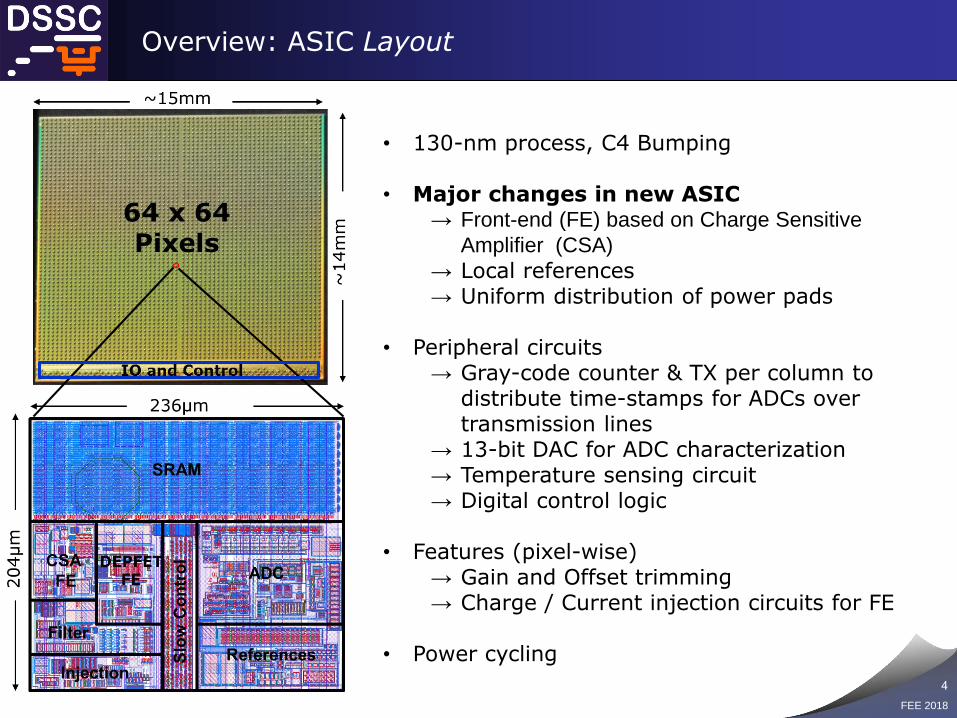
Overview: ASIC Layout
• 130-nm process, C4 Bumping
• Major changes in new ASIC→ Front-end (FE) based on Charge Sensitive
Amplifier (CSA)
→ Local references→ Uniform distribution of power pads
• Peripheral circuits→ Gray-code counter & TX per column to
distribute time-stamps for ADCs over transmission lines
→ 13-bit DAC for ADC characterization→ Temperature sensing circuit → Digital control logic
• Features (pixel-wise)→ Gain and Offset trimming→ Charge / Current injection circuits for FE
• Power cycling

FEE 2018
5
Overview: Pixel-Readout Chain
SensorA
D
DigitalMemory
Front-end
Pixel
• DEPFET• Mini-SDD
• Trapezoidal Filter• CSA + Filter
• Single-slope ADC• References
SRAM
8
SerialReadout
• Gaincompression
• Linear
• I → V & Noise
shaping
• Q → V → I
• 8/9 bit • Bias, Gain & Offset
trimming
• 800 words• Readout in ~99ms
XFEL gaps

FEE 2018
6
Overview: FE for active & passive Sensors
Two metal 4 masks either to connect CSA or DEPFET front-end (ASIC Prototype)
V → I
R
+
-
►
CQ → V
Mini-SDD Filter
●
Istat
►DEPFET
●
●●
●
● ●
Idyn
V
to ADCBump
Vreference

FEE 2018
7
Overview: FE with DEPFET as an active sensor
►
Istat + Idyn
DEPFET
+
-
Reset
►
Trapezoidal Filter
Ierr+dyn
►
Iprog
Vhold
►
Idyn
to ADC
--
S
G
CG
CL
4-bit programmablecurrent source
Vreference
Vreference 220ns
1 Pre-clear phase to remove residual charges
2 Iprog phase for bias current cancellation
Readout phase • 1st Integration: Baseline• 2nd Integration: Signal + Baseline
Clear (CL)
Clear Gate (CG)
Operation sequence:
8V
12V
Source (S)Gate (G)
2.5V4V
1 2 3
1st 2nd
Int
Ierr cancelation is done inclosed-loop configuration
3
Istat
Integration

FEE 2018
8
Overview: CSA for passive sensor
ADC
• Amplifier is based on closed-loop configuration• Coarse gain trimming (Cf , R) → 7 bits to set [0.5, 1, 2, 5, 10] keV / Bin
Schematic
CQ → V V → I
mini-SDD
Bump
Vreference

FEE 2018
9
Characterization – Setup
Main Board (MB)
Regulator Board (RB)
I/O Board(IOB)
Test condition• XFEL timing condition: 4.5-MHz frame rate • Room temperature operation• 10Hz → power cycling
• MB: Clock, Data & Power distribution (ASIC & Sensor)• RB: Power cycling & Clear pulse generation• IOB: Data concentration & DEPFET Power cycling
Focal-PaneModule
Mini-SDD Ladder DEPFET Ladder
Ladder Electronics

FEE 2018
10
Characterization – On-Chip Power Distribution
AD
C G
ain
(LSB /
V)
1st gen. ASIC: global reference
AD
C G
ain
(LSB /
V)
2nd gen. ASIC: local reference
(V)
∆V
(V)
23243 23
1.16
1.18
1.26
1.3
1.28
1.24
1.2
1.22
243
Max. Voltage drop → 140mV Max. Voltage drop → 62mV

FEE 2018
11
Characterization - Single-Slope 8-bit ADC
Peripheral
In-Pixel
13-bit DAC
Localreferences
Trimming
• Gain: 6-bit through IRamp with a resolution of ±2% (1 Bin per photon)• Offset: 4 bit through Delay with a resolution of 55 ps (Bin center)
→ single-photon resolution & minimal pixel-error rate (image fidelity)

FEE 2018
12
Characterization – ADC Gain & Linearity
0
1
LSB /
V
LSB
untrimmed
trimmed
ADU (LSB)Deviation from nom. Gain (%)
DNLGain
±2%0.07 ≤ DNL ≤ 0.4
Pix
el counts
Pix
el counts

FEE 2018
13
Characterization - Focal Plane Module Trimming
100
>99.3% have an rms value well
below 0.1 LSB (Target = 0)
1
00 200 400
0
10
38
24
4 bits are needed to reach target slope value for 16 ASIC’S. Design value → 21
>99.8% fall within ±2-% Range
around 320 LSB / V (Target)
240
320
380
Gain trimming:
IRamp trimming distribution:
Offset trimming:

FEE 2018
14
Characterization – Internal Charge Injection (mini-SDD)
10
30
40
50
20
02000500 1000 15000
AD
U (
LSB)
Default Gain settings
DAC setting
13-bit voltageDAC sets signalamplitude
Dynamic switch generates V-pulse
In-Pixel Test Input
Static column / pixel enable
• possible to adjust Cinj to match detector capacitance

FEE 2018
15
Characterization – Gain Trimming (mini-SDD)
-2 20
101
102
1
Pix
el counts
Relative slope ( %)0 2000500 1000 1500
10
30
40
50
20
0
60
70
AD
U (
LSB)
Equal Gain trimming
DAC setting
Pix
el counts
Relative slope (%)
~ 1 Bin / keV
Coarse gain:Cf (CSA), R , Cf (Filter)
Fine gain:IRamp

FEE 2018
16
Measurements – 64-by-64 Mini-SDD
Pixel 1950
Entries 780000Noise Peak 49.91Signal Peak 55.76Gain 1.01 Bin / keVENC (fit) 97.2e-
102
106
105
104
103
10
1
45 50 55 60ADU
Counts
Photo
n c
ounts
Intensity map
Pix
el counts
Bin / keV
±2%
~ 60% are with in target gain
Uncertainty in gain determinationdue to spread in Cinj
Gain
Mean → 90.15 (e-)140
100
60
20
0 40 60 80 100 120 140
ENC (e-)
0.6 1 1.20.8 1.4
100
200
300
400
500
600
Noise
5.85

FEE 2018
17
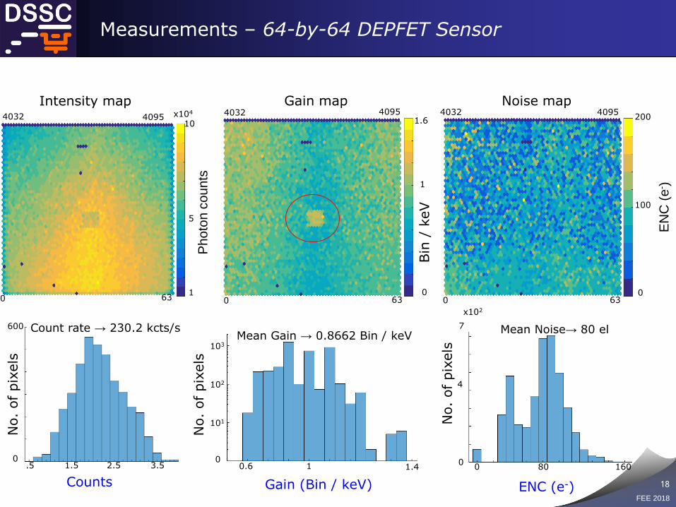
Measurements – 64-by-64 DEPFET Sensor
SRAM Address
AD
U U
nit (
LSB)
• 1 keV / Bin is successfully achieved
Photons
Offset
Fluorescence Measurements performed at PETRA III beam line
• Beam focused onto a 8 -µm thick Cu foil• Center of energy of the Cu - K∝ / Kβ → 8.155 keV
ADU Unit (LSB)
Counts
FEE 2018
18
Measurements – 64-by-64 DEPFET Sensor
0 63
4032 4095
EN
C (
e- )
0
200
100
No.
of pix
els
ENC (e-)
Mean Noise→ 80 el
0 160800
7
4
Ph
oto
n c
ou
nts
0 63
4032 4095
1
10
5
x104
x102
0
600
Counts
.5 1.5 2.5 3.5
63
4095
Bin
/ k
eV
0
1.6
1
4032
0
1.40.6 1
103
102
101
0
Mean Gain → 0.8662 Bin / keVCount rate → 230.2 kcts/s
No.
of pix
els
Gain (Bin / keV)
No.
of pix
els
Intensity map Gain map Noise map

FEE 2018
19
Measurements – 128-by-512 mini-SDD
• FPM : all ASICs fully work & both Sensors are sensitive to Light (LED)
Vacuum Chamber with FPM
• ADC-Gain & Offset trimmed for 1 Bin / keV
• FE settings
• 4.5-MHz Frame Rate
• 800-Frames
• Power Cycling
1st FPM: Single-Frame Image
100
80
00 200 400
0A
DU
(L
SB
)
FEE 2018
20
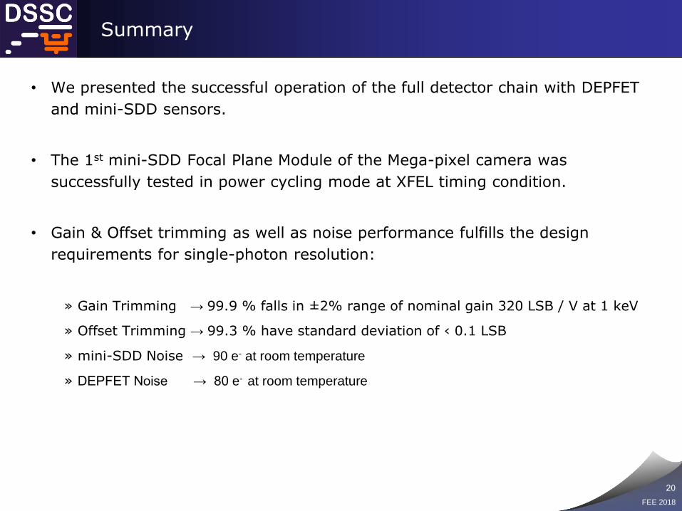
Summary
• We presented the successful operation of the full detector chain with DEPFET
and mini-SDD sensors.
• The 1st mini-SDD Focal Plane Module of the Mega-pixel camera was
successfully tested in power cycling mode at XFEL timing condition.
• Gain & Offset trimming as well as noise performance fulfills the design
requirements for single-photon resolution:
» Gain Trimming → 99.9 % falls in ±2% range of nominal gain 320 LSB / V at 1 keV
» Offset Trimming → 99.3 % have standard deviation of ‹ 0.1 LSB
» mini-SDD Noise → 90 e- at room temperature
» DEPFET Noise → 80 e- at room temperature
FEE 2018
21
Thank You