the role of silicon heterojunction and tco barriers on the
TRANSCRIPT
Research ArticleThe Role of Silicon Heterojunction and TCO Barriers on theOperation of Silicon Heterojunction Solar Cells:Comparison between Theory and Experiment
Yaser Abdulraheem ,1 Moustafa Ghannam,1
Hariharsudan Sivaramakrishnan Radhakrishnan,2 and Ivan Gordon2
1EE Department, Kuwait University, P.O. Box 5969, Safat 13060, Kuwait2Imec, Kapeldreef 75, 3001 Leuven, Belgium
Correspondence should be addressed to Yaser Abdulraheem; [email protected]
Received 30 November 2020; Accepted 4 March 2021; Published 16 March 2021
Academic Editor: Jinn Kong Sheu
Copyright © 2021 Yaser Abdulraheem et al. This is an open access article distributed under the Creative Commons AttributionLicense, which permits unrestricted use, distribution, and reproduction in any medium, provided the original work isproperly cited.
Photovoltaic devices based on amorphous silicon/crystalline silicon (a-Si:H/c-Si) heterojunction interfaces hold the highestefficiency as of date in the class of silicon-based devices with efficiencies exceeding 26% and are regarded as a promisingtechnology for large-scale terrestrial PV applications. The detailed understanding behind the operation of this type of device iscrucial to improving and optimizing its performance. SHJ solar cells have primarily two main interfaces that play a major role intheir operation: the transparent conductive oxide (TCO)/a-Si:H interface and the a-Si:H/c-Si heterojunction interface. In thework presented here, a detailed analytical description is provided for the impact of both interfaces on the performance of suchdevices and especially on the device fill factor (FF). It has been found that the TCO work function can dramatically impact theFF by introducing a series resistance element in addition to limiting the forward biased current under illumination causing thewell-known S-shape characteristic in the I-V curve of such devices. On the other hand, it is shown that the thermionic emissionbarrier at the heterojunction interface can play a major role in introducing an added series resistance factor due to the intrinsica-Si:H buffer layer that is usually introduced to improve surface passivation. Theoretical explanation on the role of bothinterfaces on device operation based on 1D device simulation is experimentally verified. The I-V characteristics of fabricateddevices were compared to the curves produced by simulation, and the observed degradation in the FF of fabricated devices wasexplained in light of analytical findings from simulation.
1. Introduction
Solar cell devices based on hydrogenated amorphous sili-con/crystalline silicon (a-Si:H/c-Si) heterojunction (SHJ)experience relatively high open-circuit voltages (VOC) andshort-circuit currents (JSC) leading to high conversion effi-ciencies (η) exceeding 26% when combined with Interdigi-tated Back Contact (IBC) technology [1]. Reduced opticallosses at the front side attributed to the IBC architectureand the relatively low recombination losses attributed to thehigh passivation quality of the SHJ (a-Si:H/c-Si) interfaceshave been accredited as the main reasons behind such a highefficiency. Such structures build upon the improved emitter
efficiency of a-Si:H/c-Si bipolar transistors [2] and originalsolar cells with the so-called heterojunction with intrinsicthin layer (HIT®) developed by the Sanyo group in 1992[3]. The main approach adopted by the Sanyo group toreduce interfacial recombination losses was to introduce athin intrinsic a-Si:H (a-Si:H(i)) layer between 5 and 8nm inthickness in between the c-Si substrate and the highly dopeda-Si:H layer where this intrinsic buffer layer would lead tohigh-quality passivation [3–5].
However, a detailed analysis of the SHJ interface hasrevealed that excellent passivation mainly arises from astrong inversion layer within the c-Si substrate, invoked byFermi potential differences due to energy band
HindawiInternational Journal of PhotoenergyVolume 2021, Article ID 6632180, 12 pageshttps://doi.org/10.1155/2021/6632180

discontinuities in the presence of chemical passivation that isachieved due to the high-quality interface between the c-Sisubstrate and the a-Si:H(i) layer [6, 7]. It has been elucidatedby Ghannam et al. that if the inversion layer carrier density isseverely impacted, then the SHJ device performance willdeteriorate despite the fact that high chemical passivation ispresent due to the a-Si:H(i) buffer layer. The presence of thisinversion layer inside the c-Si substrate close to the a-Si:H/c-Si interface has been experimentally verified and examined inthe past [8–10].
It has also been shown in detail that factors influencingthis inversion layer can have a detrimental effect on the per-formance of the device including strong degradation in thefill factor (FF) and a reduction in the open-circuit voltage(VOC) [11]. In SHJ devices, the FF is of special concern sincethe utilization of an intrinsic amorphous silicon layer causessignificant series resistance effects that have been attributedas the main cause for FF degradation [1].
It has recently been demonstrated that the FF is influ-enced by properties of the thermionic emission barrier thatis established at the a-Si:H/c-Si interface due to energy banddiscontinuities. This barrier plays a major role in the perfor-mance of SHJ devices as demonstrated by means of theoret-ical device simulations which revealed that properties of thethermionic emission barrier such as the Richardson constant,barrier height, and temperature can impact the FF since thisbarrier becomes critically responsible for carrier transportacross such interfaces [12, 13]. Other models have also sug-gested an additional transport mechanism related to quan-tum tunneling [14, 15].
On the other hand, an inadequate work function (WF)difference between the a-Si:H layer and the transparent con-ductive oxide (TCO) layer that acts as a front side (or rearside) contact can also have a detrimental effect on both theFF and VOC. This effect becomes more pronounced whenthe a-Si:H layer is of relatively low doping and/or is ultrathin.
In principle, heavy doping in the a-Si:H layer should leadto proper device operation, where the impact of the therm-ionic emission barrier or TCO Schottky barrier due to aninadequate work function is minimized. But in practice, thisis not effectively achieved where the a-Si:H layer might endup with lower effective doping due to free carrier capture bydangling bonds within a-Si:H layer [16, 17].
The purpose of the current work is to separately distin-guish the impact of the a-Si:H/c-Si and TCO/a-Si:H interfa-cial properties on device performance. In the workpresented, an a-Si:H (p+)/a-Si:H(i)/c-Si(n) structure wassimulated using the AFORS-HET device simulator. Theimpact of an inadequate TCO work function (WFTCO) andthe effect of the thermionic emission barrier on device per-formance were revealed by simulating the I-V characteristicsof two structures. The properties of the two structures simu-lated were chosen to emphasize the role of both the TCO andheterojunction interfaces on device operation and are repre-sentative of devices with high-level doping and moderate-to-low-level doping of the a-Si:H(p) layer.
The simulated I-V characteristics both in the dark andunder illumination were used to separate the impact of theTCO/a-Si:H(p+) interface (Schottky barrier interface) from
the effects of the a-Si:H(i)/c-Si interface (thermionic emis-sion barrier interface) on device behavior.
To further confirm the results of device simulation, sev-eral SHJ devices were fabricated with different dopant con-centrations in the a-Si:H(p) layer and their I-V profiles inthe dark and under illumination were measured to provideverification and validation for the device simulation results.A two-diode circuit model was also used to extract the effec-tive series resistance values for the experimental devicesunder different operational conditions.
2. Device Simulation
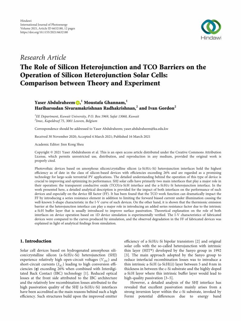
Two device structures (SHJ1 and SHJ2) have been modeledusing the AFORS-HET numerical simulation tool developedby Helmholtz-Zentrum Berlin [18]. The two structures areexactly identical except for the doping concentration in thea-Si:H(p+) layer with values of 1 × 1019 cm−3 and1× 1020 cm-3 for SHJ1 and SHJ2, respectively. The SHJ devicestructure under study is shown Figure 1 and material param-eters used in the simulations are outlined in Table 1. A200μm crystalline silicon (c-Si) substrate with n-type dopingof ND = 1:5 × 1016 cm−3 is used with an ideal ohmic backcontact. The front of the c-Si substrate, which acts as the basefor the photovoltaic device, is covered by a 5nm a-Si:H(i)intrinsic buffer layer. The interface between the a-Si:H(i)buffer layer and the c-Si(n) base is modeled as a thermionicemission barrier. On top of the buffer layer, a 10 nm highlydoped p-type a-Si:H(p+) layer is placed acting as the emitterfor the device. On top of the emitter layer, a TCO layer isplaced acting as the front contact and the optical window atthe same time. The TCO/a-Si:H(p+) interface is modeled asa Schottky barrier and is mainly controlled by the work func-tion difference between the two sides of the interface [19].
An inversion layer consisting of a high hole concentra-tion is established in the c-Si substrate adjacent to the hetero-interface as a result of energy band offsets that arise fromelectron affinity and band gap differences between amor-phous silicon and crystalline silicon, where the peak holeconcentration (reflecting a stronger inversion layer) becomeshigher for a higher active doping in the a-Si:H(p+) layer.From previous investigations [7], it has been established thatany factor negatively impacting the inversion layer wouldhave a detrimental impact on cell performance causingmainly the cell’s open-circuit voltage VOC to drop. In addi-tion, the electric field that is established around the a-Si:H/c-Si interface extends into the a-Si:H(i) buffer layerand can reach into the a-Si:H(p+) layer depending on theamount of active doping inside that layer [13]. At thermalequilibrium, the electric field established causes a majoritycarrier spillover into the intrinsic buffer layer by balancingthe diffusion of holes towards the emitter. The hole spilloverinto the intrinsic layer influences its conductivity, which inturn has a direct impact on the contribution of the intrinsicbuffer layer on the effective series resistance of the device.
In addition to the existence of a strong inversion layer,two other factors can also influence the operation of SHJsolar cell devices, impacting the FF and series resistance(RSeries). These factors include the thermionic emission
2 International Journal of Photoenergy
barrier at the a-Si:H(i)/c-Si heterointerface and the Schottkybarrier established at the a-Si:H(p+)/TCO interface [13, 15] .
The simulation study here is conducted over two parts. Inthe first part of the study, FF degradation due to effects of theSchottky interface between the TCO and the a-Si:H(p+) layeris considered. In the second part, the impact on the FF due tothe thermionic emission barrier is considered. For that part,the TCO/a-Si:H(p+) interface is taken as an ideal “flatband”ohmic contact.
2.1. Impact of the TCO/a-Si(H) Interface. In this part of thestudy, the TCO work function is altered and the impact ofsuch a variation on the FF is studied for two doping concentra-tions in the a-Si:H(p+) layer. This condition is set in order todecouple the effects of the two barriers and get to a betterunderstanding of their impact individually on the FF. It shouldalso be noted, following earlier work [7], that bulk defects inamorphous silicon have been included into the simulation fol-lowing two Gaussian profiles, acceptor-type and donor-type,with for each type, a peak concentration is equal to the dopingconcentration in the layer. As for a-Si:H/c-Si interface defects,also two Gaussian profiles are assumed with a peak concentra-tion of 1 × 1010 cm−2 eV−1, which reflects technologicallyachievable high-quality chemical passivation at the interface[20]. Additionally, both Shockley-Read-Hall and Augerrecombination mechanisms are considered, while band gapnarrowing effects were neglected for the bulk c-Si layer. The
simulation was conducted under both dark and AM1.5G illu-mination conditions. In addition, reflection losses at the frontside and losses due to parasitic absorption in the TCO layerwere ignored.
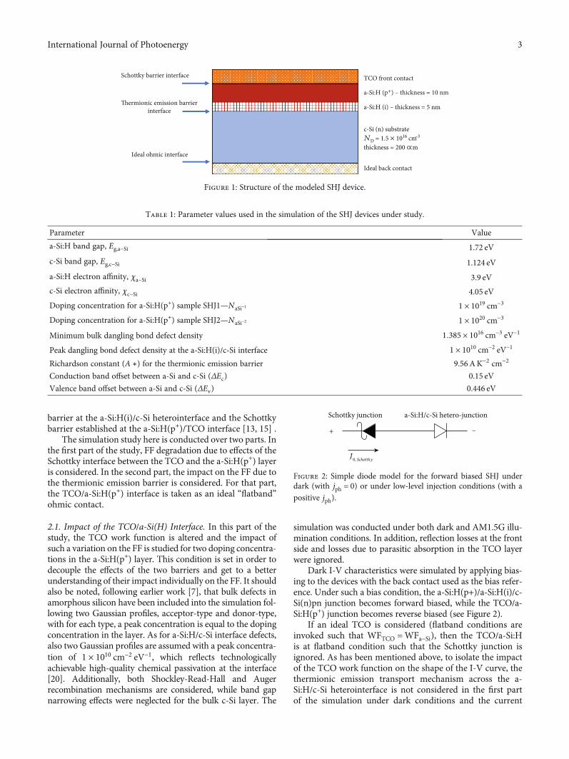
Dark I-V characteristics were simulated by applying bias-ing to the devices with the back contact used as the bias refer-ence. Under such a bias condition, the a-Si:H(p+)/a-Si:H(i)/c-Si(n)pn junction becomes forward biased, while the TCO/a-Si:H(p+) junction becomes reverse biased (see Figure 2).
If an ideal TCO is considered (flatband conditions areinvoked such that WFTCO =WFa−Si), then the TCO/a-Si:His at flatband condition such that the Schottky junction isignored. As has been mentioned above, to isolate the impactof the TCO work function on the shape of the I-V curve, thethermionic emission transport mechanism across the a-Si:H/c-Si heterointerface is not considered in the first partof the simulation under dark conditions and the current
TCO front contact
a-Si:H (p+) – thickness = 10 nm
a-Si:H (i) – thickness = 5 nm
Ideal back contact
c-Si (n) substrateND = 1.5 1016 cm–3
thickness = 200 ∝m
Schottky barrier interface
�ermionic emission barrierinterface
Ideal ohmic interface
Figure 1: Structure of the modeled SHJ device.
Table 1: Parameter values used in the simulation of the SHJ devices under study.
Parameter Value
a-Si:H band gap, Eg,a−Si 1.72 eV
c-Si band gap, Eg,c−Si 1.124 eV
a-Si:H electron affinity, χa−Si 3.9 eV
c-Si electron affinity, χc−Si 4.05 eV
Doping concentration for a-Si:H(p+) sample SHJ1—NaSi−1 1 × 1019 cm−3
Doping concentration for a-Si:H(p+) sample SHJ2—NaSi−2 1 × 1020 cm−3
Minimum bulk dangling bond defect density 1:385 × 1016 cm−3 eV−1
Peak dangling bond defect density at the a-Si:H(i)/c-Si interface 1 × 1010 cm−2 eV−1
Richardson constant (A ∗) for the thermionic emission barrier 9.56AK−2 cm−2
Conduction band offset between a-Si and c-Si (ΔEc) 0.15 eV
Valence band offset between a-Si and c-Si (ΔEv) 0.446 eV
+ –
Schottky junction a-Si:H/c-Si hetero-junction
J0, Schottky
Figure 2: Simple diode model for the forward biased SHJ underdark (with jph = 0) or under low-level injection conditions (with apositive jph).
3International Journal of Photoenergy

characteristics are simulated using the drift-diffusion carriertransport model. Three different TCO work function(WFTCO) values are considered in simulating the I-V curves,one with a flatband condition, one with aWFTCO = 5:025 eV,and one with WFTCO = 4:96 eV. Note that the value of thework function for the flatband condition is adjusted to matchthe doping level in the a-Si:H(p+) layer.
As can be seen in Figure 3, the I-V curves for both devicesunder simulation exhibit a normal behavior for a forwardbiased PN junction for the flatband case. However, once asignificant work function difference is invoked, the reversebiased Schottky junction sets the upper limit for the currentflowing through the device. If the current flowing has a valuesmaller than the Schottky junction reverse saturation current,j0Schottky , then the normal I-V exponential behavior prevails,but once the overall current approaches j0Schottky , then the I-V characteristics will experience saturation at that value sincethe reverse biased Schottky junction behavior will dominate.This current saturation behavior is clearly seen in Figure 3when the values of WFTCO = 5:025 eV and WFTCO = 4:96eV are used. It is also noticed that the saturation behaviorstrictly occurs at j0Schottky for the higher doping device SHJ2as is shown in Figure 3(b) as compared to a leaky saturationfor the lower doping device, SHJ1 (Figure 3(a)). In a cell withrelatively lower doping in the a-Si:H(p+) layer, several condi-tions play a role in shaping the I-V curve at moderate-to-highbiases when WFTCO is relatively small. For instance, high-level injection occurs early in such devices where the majoritycarrier type changes from holes to electrons, and as a result,the TCO Schottky barrier is eliminated which prevents thecurrent from saturating at j0Schottky as is shown in Figure 3.
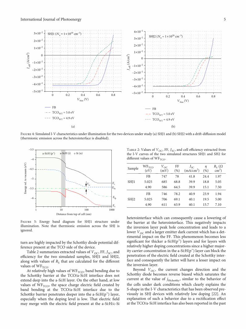
Figures 4(a) and 4(b) show the I-V behavior underAM1.5G illumination for the SHJ1 and SHJ2 devices, respec-tively. Under illumination, a photogenerated current moves
towards the TCO/a-Si:H Schottky contact and flows in theforward direction relative to the Schottky diode. At smallerWFTCO values, the voltage drop on the Schottky diode dueto the flow of such a current enhances the forward bias onthe pn junction which increases its forward current and shiftsthe maximum power point to smaller values leading to a deg-radation of the cell FF, as can be seen in Figure 4.
Equivalently, when the cell is subjected to illumination,splitting in the quasi-Fermi levels at short-circuit conditionis observed causing a potential difference for the carriers onboth sides of the heterojunction. The nature and source ofthis potential difference (referred to as the short-circuit volt-age VSC) has been previously explained in an earlier report[21]. The presence of VSC can be linked to an additionalseries resistance that will exist as the photogenerated currentcrosses the heterointerface towards the emitter which addi-tionally impacts the FF negatively. This effect is more pro-nounced for relatively low values of WFTCO and lower a-Si:H(p+) doping levels. The value of the additional seriesresistance due to the short-circuit voltage drop can be calcu-lated by extracting the short-circuit voltage VSC from thesplit in the quasi-Fermi levels obtained from the simulatedenergy band diagram for both cells. An example of the energyband diagram for SHJ1 under illumination and at short-circuit conditions is shown in Figure 5. It should be notedthat the value of VSC is calculated assuming a drift-diffusion model across the a-Si:H/c-Si heterointerface. Thevalue of the short-circuit series resistance RS is found bydividing the extracted VSC by the short-circuit current andreveals a value for RS in the range of 2Ω cm2 for both heavilyand moderately doped cells. The value of RS in this casedepends on the TCO work function as has been mentionedabove, while the value of the short-circuit voltage, VSC,depends on the position of the quasi-Fermi levels which in
0 0.2 0.4 0.6 0.8 1
J cel
l (A
/cm
2 )
FBWFTCO = 5.0 eV
WFTCO = 4.9 eV
VBias (V)
(a)J c
ell (
A/c
m2 )
0 0.2 0.4 0.6 0.8 1
FBWFTCO = 5.0 eV
WFTCO = 4.9 eV
VBias (V)
(b)
Figure 3: Simulated I-V characteristics for SHJ1 (a) and SHJ2 (b) under dark conditions withWFTCO = 5:1 eV (close to flatband condition),5.025 eV and 4.96 eV. A drift-diffusion model is invoked, and thermionic emission across the heterointerface is disabled.
4 International Journal of Photoenergy
turn are highly impacted by the Schottky diode potential dif-ference present at the TCO side of the device.
Table 2 summarizes extracted values of VOC, FF, JSC, andefficiency for the two simulated samples, SHJ1 and SHJ2,along with values of RS that are calculated for the differentvalues of WFTCO.
At relatively high values of WFTCO, band bending due tothe Schottky barrier at the TCO/a-Si:H interface does notextend deep into the a-Si:H layer. On the other hand, at lowvalues of WFTCO, the space charge electric field created byband bending at the TCO/a-Si:H interface due to theSchottky barrier penetrates deeper into the a-Si:H(p+) layer,especially when the doping level is low. That electric fieldmay merge with the electric field present at the a-Si:H/c-Si
heterointerface which can consequently cause a lowering ofthe barrier at the heterointerface. This negatively impactsthe inversion layer peak hole concentration and leads to alower VOC and a larger emitter dark current which has a det-rimental impact on the FF. This phenomenon becomes lesssignificant for thicker a-Si:H(p+) layers and for layers withrelatively higher doping concentrations since a higher major-ity carrier concentration in the a-Si:H(p+) layer can block thepenetration of the electric field created at the Schottky inter-face and consequently the latter will have a lesser impact onthe inversion layer.
Beyond VOC, the current changes direction and theSchottky diode becomes reverse biased which saturates thecurrent at the value of j0Schottky , similar to the behavior ofthe cells under dark conditions which clearly explains theS-shape in the I-V characteristics that has been observed pre-viously in SHJ devices with relatively low doping [22]. Anexplanation of such a behavior due to a rectification effectat the TCO/a-Si:H interface has also been reported in the past
1
–4
Ec
Ev
Efn
Efp
Vsc
a-Si:H (i) c-Si (n)
–6
–5.5
–5
–4.5
–3.5
Ener
gy re
l. to
vac
uum
(eV
)
Distance from top of cell (nm)10 100 1000
a-Si:H (p+)
Figure 5: Energy band diagram for SHJ1 structure underillumination. Note that thermionic emission across the SHJ isignored.
Table 2: Values of VOC, FF, JSC, and cell efficiency extracted fromthe I-V curves of the two simulated structures SHJ1 and SH2 fordifferent values of WFTCO.
SampleWFTCO(eV)
VOC(mV)
FF(%)
JSC(mA/cm2)
η(%)
RS (Ωcm2)
SHJ1
FB 747 78 41.8 24.4 1.97
5.025 685 68.8 39.9 18.8 5.05
4.90 586 64.5 39.9 15.1 7.50
SHJ2
FB 746 78.2 40.9 23.9 1.94
5.025 706 69.1 40.1 19.5 5.00
4.90 611 63.9 40.1 15.7 7.10
0 0.2 0.4 0.6 0.8
FBTCOWT = 5.0 eV
TCOWT = 4.9 eV
Vbias (V)
0
J cel
l (A
/cm
2 )
(a)
0 0.2 0.4 0.6 0.8
FBTCOWT = 5.0 eV
TCOWT = 4.9 eV
Vbias (V)
0
J cel
l (A
/cm
2 )(b)
Figure 4: Simulated I-V characteristics under illumination for the two devices under study (a) SHJ1 and (b) SHJ2 with a drift-diffusion model(thermionic emission across the heterointerface is disabled).
5International Journal of Photoenergy
[23]. The S-shape behavior in the I-V curve for the devicesunder study is clearly depicted in Figure 4.
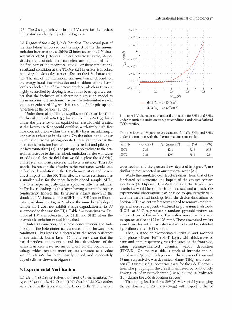
2.2. Impact of the a-Si(H)/c-Si Interface. The second part ofthe simulation is focused on the impact of the thermionicemission barrier at the a-Si:H/c-Si interface on the I-V char-acteristics of SHJ devices. Unless otherwise stated, devicestructure and simulation parameters are maintained as inthe first part of the theoretical study. For these simulations,a flatband condition at the TCO/a-Si:H interface is invokedremoving the Schottky barrier effect on the I-V characteris-tics. The size of the thermionic emission barrier depends onthe energy band discontinuities and positions of the Fermilevels on both sides of the heterointerface, which in turn arehighly controlled by doping levels. It has been reported ear-lier that the inclusion of a thermionic emission model asthe main transport mechanism across the heterointerface willlead to an enhanced VSC which is a result of hole pile-up andreflection at the barrier [13, 24].
Under thermal equilibrium, spillover of free carriers fromthe heavily doped a-Si:H(p) layer into the a-Si:H(i) layerunder the presence of an equilibrium electric field createdat the heterointerface would establish a relatively high freehole concentration within the a-Si:H(i) layer maintaining alow series resistance in the dark. On the other hand, underillumination, some photogenerated holes cannot cross thethermionic emission barrier and hence reflect and pile up atthe heterointerface [13]. The pile-up of holes close to the het-erointerface due to the thermionic emission barrier will causean additional electric field that would deplete the a-Si:H(i)buffer layer and hence increase the layer resistance. This sub-stantial increase in the effective series resistance would leadto further degradation in the I-V characteristics and have adirect impact on the FF. This effective series resistance hasa smaller value for the more heavily doped sample, SHJ2,due to a larger majority carrier spillover into the intrinsicbuffer layer, leading to this layer having a partially higherconductivity. Indeed, this behavior is clearly shown in thesimulated I-V characteristics of SHJ1 and SHJ2 under illumi-nation, as shown in Figure 6, where the more heavily dopedsample SHJ2 does not exhibit a large degradation in its FFas opposed to the case for SHJ1. Table 3 summarizes the illu-minated I-V characteristics for SHJ1 and SHJ2 when thethermionic emission model is invoked.
Under illumination, peak hole concentration and holepile-up at the heterointerface decreases under forward biasconditions. This leads to a decrease in the series resistanceof the intrinsic buffer layer [13]. It is very clear that thebias-dependent enhancement and bias dependence of theseries resistance have no major effect on the open-circuitvoltage which remains more or less constant at a valuearound 748mV for both heavily doped and moderatelydoped cells, as shown in Figure 6.
3. Experimental Verification
3.1. Details of Device Fabrication and Characterization. N-type, 180μm thick, 4.2 Ω cm, (100) Czochralski (Cz) waferswere used for the fabrication of SHJ solar cells. The solar cell
cross section and the process flow, depicted in Figure 7, aresimilar to that reported in our previous work [25].
While the simulated cell structure differs from that of thefabricated cell structure, the impact of the emitter contactinterfaces (TCO/p-a-Si:H/i-a-Si:H/c-Si) on the device char-acteristics would be similar in both cases, and as such, theexperimental observations can be used to qualitatively vali-date the theoretical findings from the device simulations ofSection 2. The as-cut wafers were etched to remove saw dam-age and were subsequently textured in potassium hydroxide(KOH) at 80°C to produce a random pyramid texture onboth surfaces of the wafers. The wafers were then laser-cutto squares of size of 125 × 125mm2. These downsized waferswere then cleaned in ozonated water, followed by a dilutedhydrofluoric acid (HF) solution.
Then, a stack of hydrogenated intrinsic and n-dopedamorphous silicon (i/n+ a-Si:H) layers with thicknesses of5 nm and 7nm, respectively, was deposited on the front side,using plasma-enhanced chemical vapor deposition(PECVD). On the rear side, a stack of intrinsic and p-doped a-Si (i/p+ a-Si:H) layers with thicknesses of 9 nm and16nm, respectively, was deposited. Silane (SiH4) and hydro-gen (H2) were used as precursor gases for the a-Si:H deposi-tion. The p-doping in the a-Si:H is achieved by additionallyflowing 2% of trimethylborane (TMB) diluted in hydrogen(H2) during the a-Si deposition process.
The doping level in the a-Si:H(p) was varied by changingthe gas flow rate of 2% TMB (QTMB) with respect to that of
0 0.2 0.4 0.6 0.8Vbias (V)
SHJ1 (Na = 1 1019 cm–3)
SHJ2 (Na = 1 1020 cm–3)
–5 10–2
–4× –2
–3 10–2
–2 10–2
–1 10–2
1 10–2
2 10–2
3 10–2
0
J cel
l (A
/cm
2 )
Figure 6: I-V characteristics under illumination for SHJ1 and SHJ2under thermionic emission transport conditions and with a flatbandTCO interface.
Table 3: Device I-V parameters extracted for cells SHJ1 and SHJ2under illumination with the thermionic emission model.
Sample VOC (mV) JSC (mA/cm2) FF (%) η (%)
SHJ1 748 42.1 52.3 16.5
SHJ2 748 40.9 75.3 23
6 International Journal of Photoenergy

SiH4 (QSiH4). The different conditions used in this work are
summarized in Table 4. For the reference condition, TMB50/50, the QTMB : QSiH4
ratio was 1 : 1, corresponding to 2%of TMB in SiH4 in the gas mixture. This corresponds to a highdoping level in the a-Si:H(p). To evaluate the effect of lowerdoping levels in the a-Si:H(p) layer on the transport character-istics of this heterocontact, three additional splits in the a-Si:H(p) layer depositions, with QTMB : QSiH4
ratios of 1 : 5,1 : 7.5, and 1 : 10, corresponding to 0.4%, 0.27%, and 0.2% ofTMB in SiH4 in the gas mixture, were also tested in this study.The H2 flow rate (QH2
) was kept constant for all splits.Minority carrier lifetime measurements were performed
using the quasi-steady-state photoconductance (QSSPC)method to evaluate the passivation quality, while photolumi-nescence (PL) imaging was performed to evaluate the passiv-ation uniformity. In the next step, the wafers were againcleaned in HF solution to remove any native oxide on thea-Si:H surfaces. Then, indium tin oxide (ITO) was depositedon both surfaces by DC sputtering through a shadow maskwith an opening of 40 × 40mm2, which defines the area ofthe cell. In this way, 4 cell areas are defined per wafer. Finally,screen printing of the front and rear contacts was done usinga low-temperature Ag paste, which is cured at 160°C for~25min in N2 in a belt furnace. The wafers were then againlaser-diced to produce 4 individual cells from each wafer. Atotal of 8 cells were fabricated for each split. Illuminatedcurrent-voltage (I-V) measurements were then done usingthe AM1.5G spectrum in a solar simulator at 25°C, under 1sun intensity, using an aperture area of 15.95 cm2.
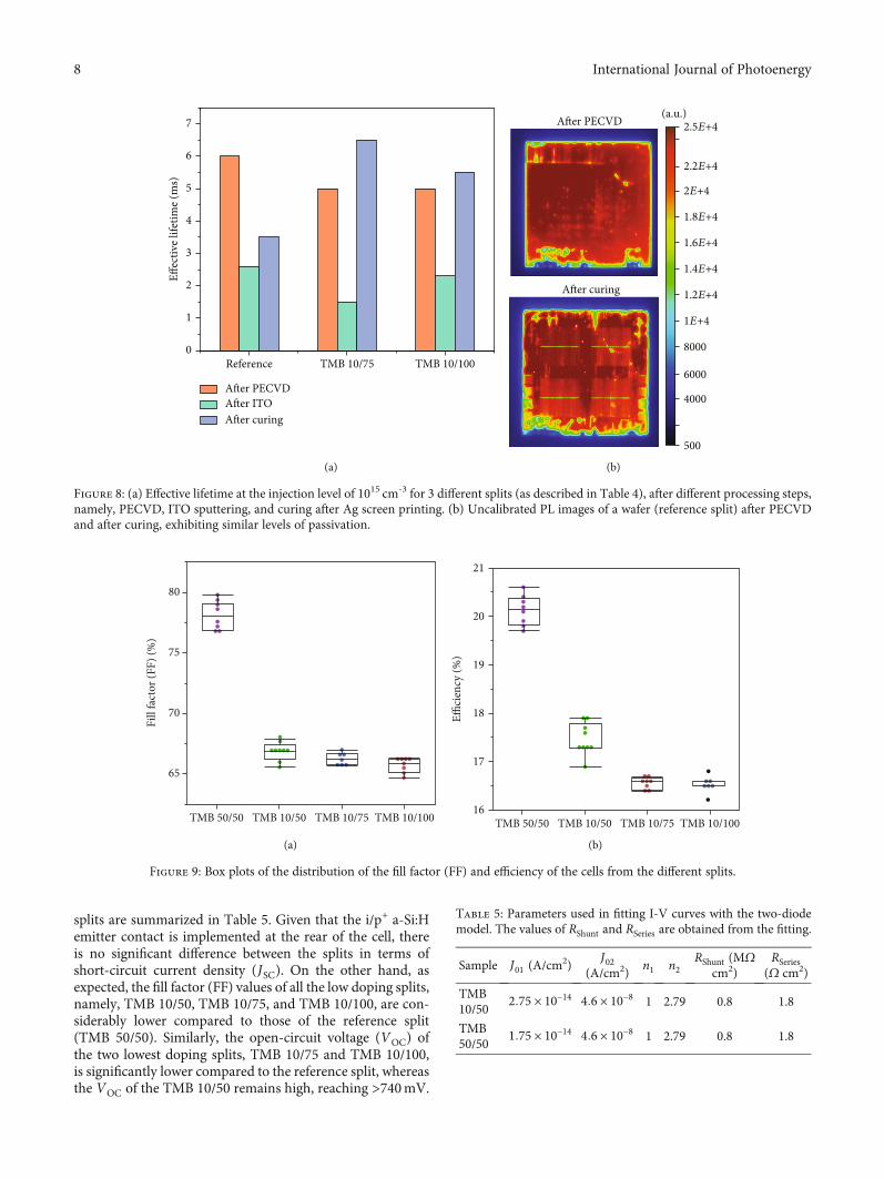
3.2. Device Performance Results. Minority carrier lifetimemeasurements show that wafers from all the splits exhibitexcellent and similar surface passivation, as plotted inFigure 8, with lifetimes in the range of ~5-6ms at an injectionlevel of 1015 cm-3. After ITO deposition, the lifetimes drop toaround 2.1-2.6ms due to damage from sputtering. However,this passivation loss is fully recovered for most of the wafersduring the curing step after screen printing, whereby thewafers are subjected to an 160°C anneal in N2 for around25min. Thus, there are no major differences in terms of pas-sivation quality between the different i/p+ a-Si:H splits, indi-cating that the lower doping levels of the a-Si:H(p) layersused in this work do not affect the passivation qualityadversely.
The FF and efficiency for all fabricated samples are plot-ted in Figures 9(a) and 9(b), respectively, while the lowest,best, and average light I-V cell parameters of the different
AgAg
Ag
ITO
n-type c-Si
ITO
i/n+ a-Si:H(electron contact)
i/p+ a-Si:H(hole contact)
(a)
Texturing + cleaning
Front i/n+ a-Si PECVD (electron contact)
Rear i/p+ a-Si PECVD (hole contact)
ITO sputtering (front and rear)
Ag screen-printing (front and rear)
2
(b)
Figure 7: The cross-sectional schematic (a) and the process flow (b) of silicon heterojunction solar cells.
Table 4
(a) Gas flow rates of silane (QSiH4) and 2% TMB in H2 (QH2
) used forthe deposition of p-a-Si:H, and the corresponding flow ratios andTMB % in SiH4 in the gas mixture. The H2 flow rate (QH2
) waskept constant
Splitname
Gas flow rates (sccm)QTMB/QSiH4
TMB %in SiH4
2% TMB inH2 (QTMB)
Silane(QSiH4
)
TMB50/50
Reference1
50 50 1 2
TMB10/50
Lowdoping 1
10 50 0.2 0.4
TMB10/75
Lowdoping 2
10 75 0.13 0.27
TMB10/100
Lowdoping 3
10 100 0.1 0.2
(b) Summary of the lowest, average, and best light I-V parameters ofcells from the different splits of a-Si:H(p) devices
Split
Short-circuitcurrent
density, JSC(mA/cm2)
Open-circuitvoltage,
VOC (mV)
Fillfactor,FF (%)
Efficiency,η (%)
TMB50/50
Lowest 35.1 729.5 76.8 19.7
Avg 35.2 733 78.1 20.1
Best 35.4 735 79.1 20.6
TMB10/50
Lowest 34.9 738 65.7 16.9
Avg 35.2 741 66.8 17.5
Best 35.5 742 67.9 17.9
TMB10/75
Lowest 35.0 705.8 66.7 16.5
Avg 35.0 714 66.2 16.5
Best 35.2 712 67.0 16.8
TMB10/100
Lowest 35.3 702.3 66.1 16.4
Avg 35.3 715 65.7 16.5
Best 35.3 720 65.7 16.7
7International Journal of Photoenergy
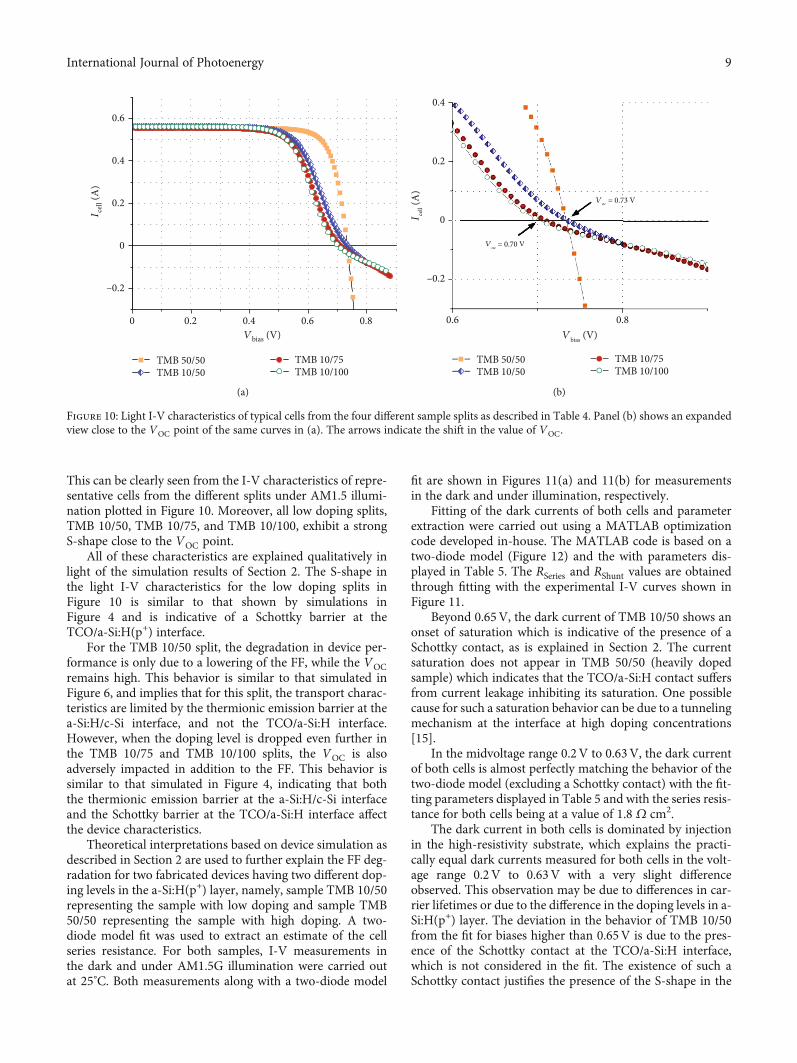
splits are summarized in Table 5. Given that the i/p+ a-Si:Hemitter contact is implemented at the rear of the cell, thereis no significant difference between the splits in terms ofshort-circuit current density (JSC). On the other hand, asexpected, the fill factor (FF) values of all the low doping splits,namely, TMB 10/50, TMB 10/75, and TMB 10/100, are con-siderably lower compared to those of the reference split(TMB 50/50). Similarly, the open-circuit voltage (VOC) ofthe two lowest doping splits, TMB 10/75 and TMB 10/100,is significantly lower compared to the reference split, whereasthe VOC of the TMB 10/50 remains high, reaching >740mV.
Reference TMB 10/75 TMB 10/1000
1
2
3
4
5
6
7
Effec
tive l
ifetim
e (m
s)
A�er PECVDA�er ITOA�er curing
(a)
A�er PECVD (a.u.)
500
4000
6000
8000
1E+4
1.2E+4
1.4E+4
1.6E+4
1.8E+4
2E+4
2.2E+4
2.5E+4
A�er curing
(b)
Figure 8: (a) Effective lifetime at the injection level of 1015 cm-3 for 3 different splits (as described in Table 4), after different processing steps,namely, PECVD, ITO sputtering, and curing after Ag screen printing. (b) Uncalibrated PL images of a wafer (reference split) after PECVDand after curing, exhibiting similar levels of passivation.
65
TMB 50/50 TMB 10/50 TMB 10/75 TMB 10/100
70
75
Fill
fact
or (F
F) (%
)
80
(a)
16
17
18
19
20
21
TMB 50/50 TMB 10/50 TMB 10/75 TMB 10/100
Effici
ency
(%)
(b)
Figure 9: Box plots of the distribution of the fill factor (FF) and efficiency of the cells from the different splits.
Table 5: Parameters used in fitting I-V curves with the two-diodemodel. The values of RShunt and RSeries are obtained from the fitting.
Sample J01 (A/cm2)
J02(A/cm2)
n1 n2RShunt (MΩ
cm2)RSeries
(Ω cm2)
TMB10/50
2:75 × 10−14 4:6 × 10⁻⁸ 1 2.79 0.8 1.8
TMB50/50
1:75 × 10−14 4:6 × 10⁻⁸ 1 2.79 0.8 1.8
8 International Journal of Photoenergy
This can be clearly seen from the I-V characteristics of repre-sentative cells from the different splits under AM1.5 illumi-nation plotted in Figure 10. Moreover, all low doping splits,TMB 10/50, TMB 10/75, and TMB 10/100, exhibit a strongS-shape close to the VOC point.
All of these characteristics are explained qualitatively inlight of the simulation results of Section 2. The S-shape inthe light I-V characteristics for the low doping splits inFigure 10 is similar to that shown by simulations inFigure 4 and is indicative of a Schottky barrier at theTCO/a-Si:H(p+) interface.
For the TMB 10/50 split, the degradation in device per-formance is only due to a lowering of the FF, while the VOCremains high. This behavior is similar to that simulated inFigure 6, and implies that for this split, the transport charac-teristics are limited by the thermionic emission barrier at thea-Si:H/c-Si interface, and not the TCO/a-Si:H interface.However, when the doping level is dropped even further inthe TMB 10/75 and TMB 10/100 splits, the VOC is alsoadversely impacted in addition to the FF. This behavior issimilar to that simulated in Figure 4, indicating that boththe thermionic emission barrier at the a-Si:H/c-Si interfaceand the Schottky barrier at the TCO/a-Si:H interface affectthe device characteristics.
Theoretical interpretations based on device simulation asdescribed in Section 2 are used to further explain the FF deg-radation for two fabricated devices having two different dop-ing levels in the a-Si:H(p+) layer, namely, sample TMB 10/50representing the sample with low doping and sample TMB50/50 representing the sample with high doping. A two-diode model fit was used to extract an estimate of the cellseries resistance. For both samples, I-V measurements inthe dark and under AM1.5G illumination were carried outat 25°C. Both measurements along with a two-diode model
fit are shown in Figures 11(a) and 11(b) for measurementsin the dark and under illumination, respectively.
Fitting of the dark currents of both cells and parameterextraction were carried out using a MATLAB optimizationcode developed in-house. The MATLAB code is based on atwo-diode model (Figure 12) and the with parameters dis-played in Table 5. The RSeries and RShunt values are obtainedthrough fitting with the experimental I-V curves shown inFigure 11.
Beyond 0.65V, the dark current of TMB 10/50 shows anonset of saturation which is indicative of the presence of aSchottky contact, as is explained in Section 2. The currentsaturation does not appear in TMB 50/50 (heavily dopedsample) which indicates that the TCO/a-Si:H contact suffersfrom current leakage inhibiting its saturation. One possiblecause for such a saturation behavior can be due to a tunnelingmechanism at the interface at high doping concentrations[15].
In the midvoltage range 0.2V to 0.63V, the dark currentof both cells is almost perfectly matching the behavior of thetwo-diode model (excluding a Schottky contact) with the fit-ting parameters displayed in Table 5 and with the series resis-tance for both cells being at a value of 1.8 Ω cm2.
The dark current in both cells is dominated by injectionin the high-resistivity substrate, which explains the practi-cally equal dark currents measured for both cells in the volt-age range 0.2V to 0.63V with a very slight differenceobserved. This observation may be due to differences in car-rier lifetimes or due to the difference in the doping levels in a-Si:H(p+) layer. The deviation in the behavior of TMB 10/50from the fit for biases higher than 0.65V is due to the pres-ence of the Schottky contact at the TCO/a-Si:H interface,which is not considered in the fit. The existence of such aSchottky contact justifies the presence of the S-shape in the
0
TMB 50/50
–0.2
0
0.2
0.4
0.6
TMB 10/50TMB 10/75TMB 10/100
0.2 0.4 0.6 0.8Vbias (V)
I cel
l (A
)
(a)
TMB 50/50
–0.2
0.6 0.8
0
0.2
0.4
TMB 10/50TMB 10/75TMB 10/100
Vbias (V)
Voc = 0.70 V
Voc = 0.73 V
I cell (A
)
Voc = 0.70 V
Voc = 0.73 V
(b)
Figure 10: Light I-V characteristics of typical cells from the four different sample splits as described in Table 4. Panel (b) shows an expandedview close to the VOC point of the same curves in (a). The arrows indicate the shift in the value of VOC.
9International Journal of Photoenergy

I-V characteristics under illumination for sample TMB 10/50as shown in Figure 11(b).
On the other hand, the sample with high doping (TMB50/50) does not show this effect, which agrees very well withthe behavior of the dark current and the assumption oftunneling discussed above. Although current saturation inthe I-V characteristics under illumination beyond VOC con-firms the presence of a Schottky diode in TMB 10/50, yetdepletion of a- Si:H(p+) layer is not so severe in this cell suchthat the impact of the TCO/Si:H interface on VOC is notdominant. This explains why for both cells, VOC is similaras is clearly evident in Figure 11.
On the other hand, VOC is found to be degraded in cellTMB 10/100 with even less doping due to more severe deple-tion, as depicted in Figure 10. Consequently, the severe deg-radation of the measured FF to a value around 67% for thelow doping sample TMB 10/50 can be attributed to a realresistance enhancement under illumination. This can be fur-ther validated by the perfect fitting of the I-V characteristicsunder illumination that is obtained when the cell series resis-tance is enhanced from its value of 1.8 Ω cm2 in the dark toan average value of 3.8Ω cm2 throughout the whole voltagerange under illumination. On the other hand, the fitting ofcell TMB 50/50 can be perfectly obtained keeping the series
resistance unchanged under illumination, which agrees verywell with the interpretation of negligible resistance enhance-ment in cells with heavily doped a-Si:H(p+) and with theabsence of a Schottky effect, in accordance to the explanationpresented in Section 2.
4. Summary and Conclusions
A detailed understanding behind the operation of SHJdevices and what affects their performance is explained basedon an analytical model. Such a model is crucial in identifyingthe exact mechanisms of degradation in SHJ devices and canaid their technological improvement. The SHJ device com-prises of two main interfaces, namely, the TCO/a-Si:H inter-face and the a-Si:H/c-Si interface. By isolating the impact ofeach interface on the I-V characteristics for SHJ devicesunder dark and light conditions, it was possible to analyzethe root cause of cell performance degradation whether itwas mainly from the properties of the TCO/a-Si:H interfaceor from the a-Si:H/c-Si interface due to thermionic emission.The appearance of an S-shape in the I-V characteristics ofSHJ solar cells was also explained based on a rectificationaction that can be present at the TCO/a-Si:H interface as aresult of an inadequate TCO work function. On the otherhand, degradation associated with the thermionic emissionbarrier was shown to be limited to the FF and is caused bya real enhancement in the cell series resistance especiallywhen the free hole concentration in the a-Si:H(p+) layer isnot high enough to considerably spill over into the ultrathinintrinsic a-Si:H(i) buffer layer. Under illumination, the lattermay be totally depleted which causes a significant increase inthe cell series resistance thereby degrading the FF withoutaffecting the value of VOC. This behavior was clearly demon-strated and explained in this work through device
0.2 0.3 0.4 0.5 0.6 0.7 0.8Vbias (V)
TMB 50/50TMB 10/502-diode model fit
(a)
0.20 0.4 0.6 0.8Vbias (V)
TMB 50/50TMB 10/502-diode model fit
0
(b)
Figure 11: I-V characteristics for samples TMB 10/50 and TMB 50/50 under (a) dark conditions and (b) light conditions, both with the 2-diode model fitting.
I01 I02RSeriesI
VRShIPh
n2
D2
n1
D1
Figure 12: Schematic of the two-diode model used for the I-V curvefitting.
10 International Journal of Photoenergy
simulations and was experimentally confirmed by studyingthe I-V characteristics of fabricated SHJ devices in the darkand under illumination. Devices with relatively low dopingexhibited an S-shape in the I-V characteristics indicating aSchottky rectification effect and possibly a-Si:H depletionimpacting directly the cells’ FF and VOC, hence degradingdevice efficiency.
Data Availability
The data are available on request by contacting the corre-sponding author, Yaser Abdulraheem([email protected]).
Conflicts of Interest
The authors declare no conflict of interest.
Authors’ Contributions
Authors have made significant contribution to this study andhave approved this submission.
Acknowledgments
The work was funded partially by the Kuwait Foundation forthe Advancement of Sciences under project code: CN18-15EE-01. This work was partially conducted by the KuwaitUniversity Research Administration General Facilities (pro-ject GE01/08).
References
[1] K. Yoshikawa, H. Kawasaki, W. Yoshida et al., “Silicon hetero-junction solar cell with interdigitated back contacts for aphotoconversion efficiency over 26%,” Nature Energy, vol. 2,no. 5, pp. 1552–1558, 2017.
[2] M. Ghannam, J. Nijs, R. Mertens, and R. DeKeersmaecker, “Asilicon bipolar transistor with a hydrogenated amorphousemitter,” in 1984 International Electron Devices Meeting,pp. 746–748, San Francisco, CA, USA, 1984.
[3] M. Tanaka, M. Taguchi, T. Matsuyama et al., “Development ofnew a-Si/c-Si heterojunction solar cells: ACJ-HIT (artificiallyconstructed junction-heterojunction with intrinsic thin-layer),” Japanese Journal of Applied Physics, vol. 31,pp. 3518–3522, 1992.
[4] M. Taguchi, K. Kawamoto, S. Tsuge et al., “HITTM cells—high-efficiency crystalline Si cells with novel structure,” Progress inPhotovoltaics: Research and Applications, vol. 8, no. 5,pp. 503–513, 2000.
[5] M. Taguchi, A. Terakawa, E. Maruyama, and M. Tanaka,“Obtaining a higherVoc in HIT cells,” Progress in Photovoltaics:Research and Applications, vol. 13, no. 6, pp. 481–488, 2005.
[6] J. Furlan, P. Popović, F. Smole, and M. Topič, “Analyticalmodel of a-Si/c-Si HIT solar cell,” MRS Online ProceedingsLibrary Archive, vol. 420, p. 261, 2011.
[7] M. Ghannam, G. Shehadah, Y. Abdulraheem, andJ. Poortmans, “On the possible role of the interfacial inversionlayer in the improvement of the performance of hydrogenatedamorphous silicon/crystalline silicon heterojunction solar cells
[HIT],” Solar Energy Materials and Solar Cells, vol. 132, no. C,pp. 320–328, 2015.
[8] J. P. Kleider, A. S. Gudovskikh, and P. Roca i Cabarrocas,“Determination of the conduction band offset between hydro-genated amorphous silicon and crystalline silicon from surfaceinversion layer conductance measurements,” Applied PhysicsLetters, vol. 92, no. 16, p. 162101, 2008.
[9] R. Varache, J. P. Kleider, W. Favre, and L. Korte, “Band bendingand determination of band offsets in amorphous/crystalline siliconheterostructures from planar conductance measurements,” Jour-nal of Applied Physics, vol. 112, no. 12, p. 123717, 2012.
[10] K. Ghosh, C. Tracy, and S. Bowden, “Experimental and theo-retical verification of the presence of inversion region in a-Si/c-Si heterojunction solar cells with an intrinsic layer,” in2012 38th IEEE Photovoltaic Specialists Conference,pp. 001046–001048, Austin, TX, USA, 2012.
[11] M. Ghannam, Y. Abdulraheem, and G. Shehada, “Interpreta-tion of the degradation of silicon HIT solar cells due to inade-quate front contact TCO work function,” Solar EnergyMaterials and Solar Cells, vol. 145, no. 3, pp. 423–431, 2016.
[12] T. F. Schulze, L. Korte, E. Conrad, M. Schmidt, and B. Rech,“Electrical transport mechanisms in a-Si:H/c-Si heterojunc-tion solar cells,” Journal of Applied Physics, vol. 107, no. 2,p. 023711, 2010.
[13] M. Ghannam and Y. Abdulraheem, “Electro-physical interpre-tation of the degradation of the fill factor of silicon heterojunc-tion solar cells due to incomplete hole collection at the a-Si:H/c-Si thermionic emission barrier,” Applied Sciences,vol. 8, no. 10, p. 1846, 2018.
[14] M. W. M. V. Cleef, F. A. Rubinelli, and R. E. I. Schropp,“Effects of band offsets ona-Sic:H/c-Si heterojunction solar cellperformance,” MRS Online Proceedings Library Archive,vol. 507, p. 125, 1998.
[15] A. Kanevce andW. K. Metzger, “The role of amorphous siliconand tunneling in heterojunction with intrinsic thin layer (HIT)solar cells,” Journal of Applied Physics, vol. 105, no. 9,p. 094507, 2009.
[16] M. Stutzmann, D. K. Biegelsen, and R. A. Street, “Detailedinvestigation of doping in hydrogenated amorphous siliconand germanium,” Physical Review B, vol. 35, no. 11,pp. 5666–5701, 1987.
[17] S. De Wolf, C. Ballif, and M. Kondo, “Kinetics ofa-Si:H bulkdefect anda-Si:H/c-Si interface-state reduction,” PhysicalReview B, vol. 85, no. 11, p. 113302, 2012.
[18] R. Varache, C. Leendertz, M. E. Gueunier-Farret, J. Haschke,D. Muñoz, and L. Korte, “Investigation of selective junctionsusing a newly developed tunnel current model for solar cellapplications,” Solar Energy Materials and Solar Cells,vol. 141, no. C, pp. 14–23, 2015.
[19] E. Centurioni and D. Iencinella, “Role of front contact workfunction on amorphous silicon/crystalline silicon heterojunc-tion solar cell performance,” IEEE Electron Device Letters,vol. 24, no. 3, pp. 177–179, 2001.
[20] A. Froitzheim, K. Brendel, L. Elstner, W. Fuhs, K. Kliefoth, andM. Schmidt, “Interface recombination in heterojunctions ofamorphous and crystalline silicon,” Journal of Non-Crystalline Solids, vol. 299, pp. 663–667, 2002.
[21] M. Ghannam and Y. Abdulraheem, “Fundamental constraintsimposed by energy barriers on the fill factor and on the effi-ciency of silicon heterojunction solar cells,” Solar EnergyMate-rials and Solar Cells, vol. 171, pp. 228–238, 2017.
11International Journal of Photoenergy
[22] M. Bivour, S. Schröer, and M. Hermle, “Numerical Analysis ofElectrical TCO / a-Si:H(p) Contact Properties for Silicon Het-erojunction Solar Cells,” Energy Procedia, vol. 38, pp. 658–669,2013.
[23] S. Kirner, M. Hartig, L. Mazzarella et al., “The influence of ITOdopant density on J-V characteristics of silicon heterojunctionsolar cells: experiments and simulations,” Energy Procedia,vol. 77, pp. 725–732, 2015.
[24] Y. Hayashi, D. Li, A. Ogura, and Y. Ohshita, “Role of i-aSi:Hlayers in aSi:H/cSi heterojunction solar cells,” IEEE Journal ofPhotovoltaics, vol. 3, no. 4, pp. 1149–1155, 2013.
[25] T. Bearda, A. Umer, S. Jambaldinni et al., “Fabrication of sili-con heterojunction cells on 50μm epitaxial substrates,” in33rd European Photovoltaic Solar Energy Conference and Exhi-bition - EUPVSEC, pp. 765–767, Amsterdam, The Netherland,2017.
12 International Journal of Photoenergy