the simplest digital moving average filter
TRANSCRIPT
Tiago Davi Curi Busarello Jan/2014
Digital Moving Average Filter and its Dynamic Behavior
A moving average filter is a digital filter whose main function is to calculate the average value from a signal.
There are several manners to do it. Here, it will be presented one of the simplest manner. It consists only of
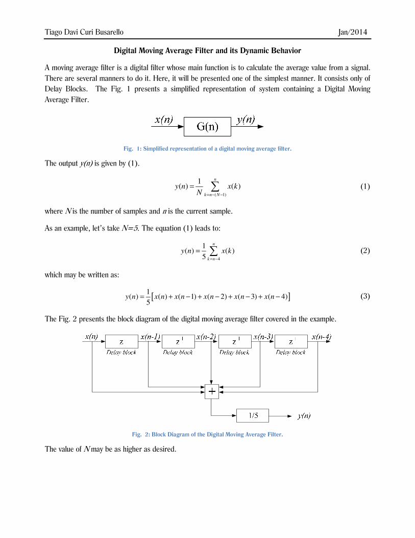
Delay Blocks. The Fig. 1 presents a simplified representation of system containing a Digital Moving
Average Filter.
Fig. 1: Simplified representation of a digital moving average filter.
The output y(n) is given by (1).
( 1)
1( ) ( )
n
k n N
y n x kN = − −
= ∑ (1)
where N is the number of samples and n is the current sample.
As an example, let’s take N=5. The equation (1) leads to:
4
1( ) ( )
5
n
k n
y n x k= −
= ∑ (2)
which may be written as:
[ ]1
( ) ( ) ( 1) ( 2) ( 3) ( 4)5
y n x n x n x n x n x n= + − + − + − + − (3)
The Fig. 2 presents the block diagram of the digital moving average filter covered in the example.
Fig. 2: Block Diagram of the Digital Moving Average Filter.
The value of N may be as higher as desired.
Simulation and Experimental Results
A Moving Average Filter is simulated in PSIM and experimentally tested in the float-point digital signal
processor TMS320F28335. Two different signals are applied separately as input. It will be presented
results for N=27 and N=54. Additionally, a step is made in the input signal and the filter dynamic behavior
is evaluated. The digital results are obtained experimentally by means of a DAC (Digital-Analog
Converter).
1) Sinusoidal signal as input
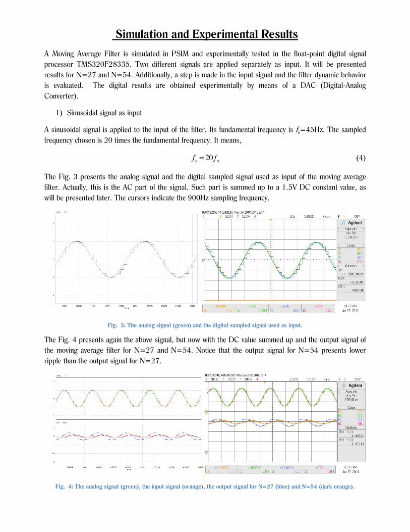
A sinusoidal signal is applied to the input of the filter. Its fundamental frequency is fo=45Hz. The sampled
frequency chosen is 20 times the fundamental frequency. It means,
20s o
f f= (4)
The Fig. 3 presents the analog signal and the digital sampled signal used as input of the moving average
filter. Actually, this is the AC part of the signal. Such part is summed up to a 1.5V DC constant value, as
will be presented later. The cursors indicate the 900Hz sampling frequency.
Fig. 3: The analog signal (green) and the digital sampled signal used as input.
The Fig. 4 presents again the above signal, but now with the DC value summed up and the output signal of
the moving average filter for N=27 and N=54. Notice that the output signal for N=54 presents lower
ripple than the output signal for N=27.
Fig. 4: The analog signal (green), the input signal (orange), the output signal for N=27 (blue) and N=54 (dark orange).
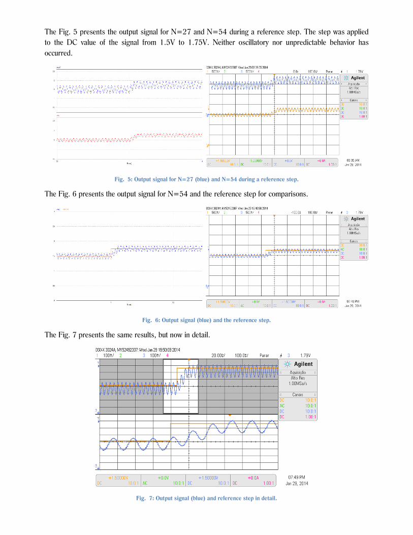
The Fig. 5 presents the output signal for N=27 and N=54 during a reference step. The step was applied
to the DC value of the signal from 1.5V to 1.75V. Neither oscillatory nor unpredictable behavior has
occurred.
Fig. 5: Output signal for N=27 (blue) and N=54 during a reference step.
The Fig. 6 presents the output signal for N=54 and the reference step for comparisons.
Fig. 6: Output signal (blue) and the reference step.
The Fig. 7 presents the same results, but now in detail.
Fig. 7: Output signal (blue) and reference step in detail.

2) Distorted signal as input
The Fig. 8 presents the analog signal and the digital sampled signal used as input. The input signal is a
sinusoidal summed up to the 25%, related to the fundamental, of 3rd harmonic component.
Fig. 8: Analog signal (green) and the digital sampled signal used as input.
The Fig. 9 presents the input and output signal during a reference step for N=54.
Fig. 9: Input (blue) and Output signal for N=54 (orange).
The Fig. 10 presents the dynamic behavior of the output signal during the start-up. The reference DC value
was set to 2.25V. The steady-state condition is achieved without an unpredictable behavior. The 1.7
constant value before the start-up is presented due to the initial condition of the used DAC.

Fig. 10: Dynamic behavior during the start-up.
The Fig. 11 presents a part of the simulated circuit.
Fig. 11: A part of the simulated circuit
Hardware
F28335
Config
ADC
A0
B7
A1
A2
A3
A4
A5
A6
A7
B0
B1
B2
B3
B4
B5
B6
D0
D15
D1
D2
D3
D4
D5
D6
D7
D8
D9
D10
D11
D12
D13
D14
F28335
145 V Vanalog
ZOHfs
V Vdig
V Vin
1
z
fs
File
1
z
fs1
z
fs1
z
fs1
z
fs1
z
fs1
z
fs1
z
fs1
z
fs
45*30.25
1.5
CS0
CS1
CS2
CS3
F28335
SPI ConfigD0
D6
D7
D0
DOUT
D1
D2
D3
D4
D5
D7
D1
D2D3
D4
D5
D6
F28335
GPIO14CS0CS1
CS2
CS3
Sync
Intr
SPI Device
F28335
MCP4922
DSPClock
F28335
SPI
F28335
out
ZOH
fsV VDAC3
DAC3
ZOH
fs V VDAC4
DAC4 SPI
F28335
out
DAC3Vref_step

The complete simulation file with Automatic Code Generation used in this project is available for free on
https://sites.google.com/site/busarellosmartgrid/
Reference:
[1] Richard G. Lyons. “Understanding Digital Signal Processing” Third Edition, Prentice Hall, 2011.