the summary of rf 1800 mini usb programmer
TRANSCRIPT

Chapter 1 Summary
1.1 Main Functions
RF series USB General Programmer is mainly used to write
in programmable devices, including: EPROM, FLASHROM, EEPROM,
serial EEPROM, Programmable Logic Device(PLD), and Micro
Process Unit(MPU). Besides, it could be used to implement
function testing, unknown model identifying for some common
devices, mostly for TTL74/75 series, CMOS40/45 series, SRAM
and some interface devices.
Besides above-mentioned functions, Programmer of
RF-3148USB, RF-2148USB, RF-1800miniUSB type could be used to
directly read GAL16V8/A/B, 20V8/A/B, PALCE16V8H, 20V8H.
Automatic conversion function from JEDEC to logic expression
is available.
1.2 Software Features
The Windows version software of RF series Programmer is
of bilingual mode in Chinese & English. When Chinese mode is
selected, all the work options, running status, running results
will be displayed in Chinese.
Common works could be selected conveniently by click on
icons.
In the Windows version software of RF series Programmer,
explanation of every mouse-pointed operation, supposed to be
helpful for the beginners, could be found in the status bar
of Chinese notes.
1.3 Hardware & software composition
Hardware of RF—3148USB, RF—1800miniUSB, RF—910USB
Programmer consists of main frame, USB link cable, USB power
cable.
Hardware of RF—2148USB Programmer consists of main frame,
power supply, link cable.
Software of Windows version is in a compact disc. Chinese
Manual, product warranty card are also available.
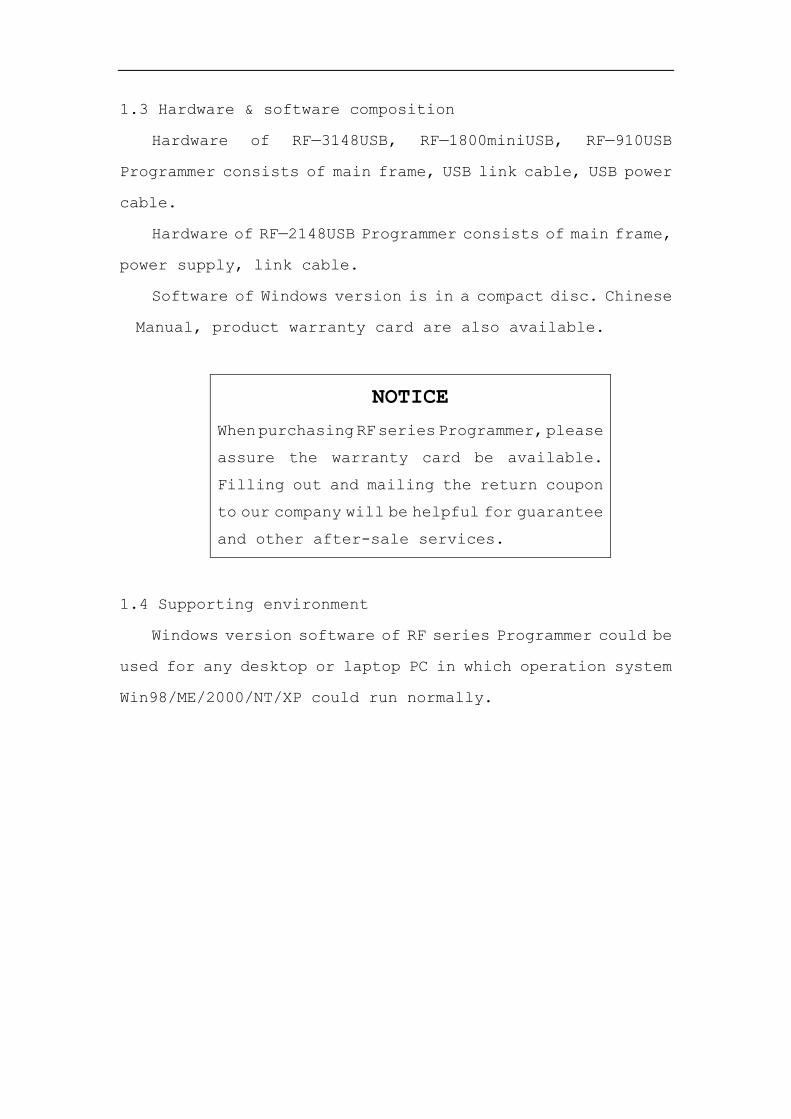
NOTICE
When purchasing RF series Programmer, please
assure the warranty card be available.
Filling out and mailing the return coupon
to our company will be helpful for guarantee
and other after-sale services.
1.4 Supporting environment
Windows version software of RF series Programmer could be
used for any desktop or laptop PC in which operation system
Win98/ME/2000/NT/XP could run normally.

Chapter 2 Hardware & Software Setup
2.1 Hardware setup
2.1.1 Cable connection for Programmer RF—2148USB
Connect one end of USB cable to PC USB interface, the other
end to the Programmer mainframe. The programmer is supplied
power by external power supply. When turn on the Programmer
mainframe power switch, the indicator should be on, indicating
the power supply is normal.
2.1.2 For Programmer RF-3148USB, RF-1800miniUSB, RF-910USB,
there are two cable connection modes:
2.1.2.1 Power supplied by only USB, shown as below
Low power devices, such as USB mouse or U disk
Or idle
In this mode, the programmer is supplied power by only
the mainframe USB interface, without any external DC power
supply. Since power capacity of USB interface is limited (less
than 500mA), for reliability reason, double USB interfaces
are used for power supply. In this mode, USB1 is used for
communicating with the programmer and providing communication
power supply, USB2 is used for cautery power supply. For users’
convenience, low power devices, such as USB mouse, U disk,
are allowed to connect with USB2 at the same time.
USB1
PC USB2
USB
cautery power supply
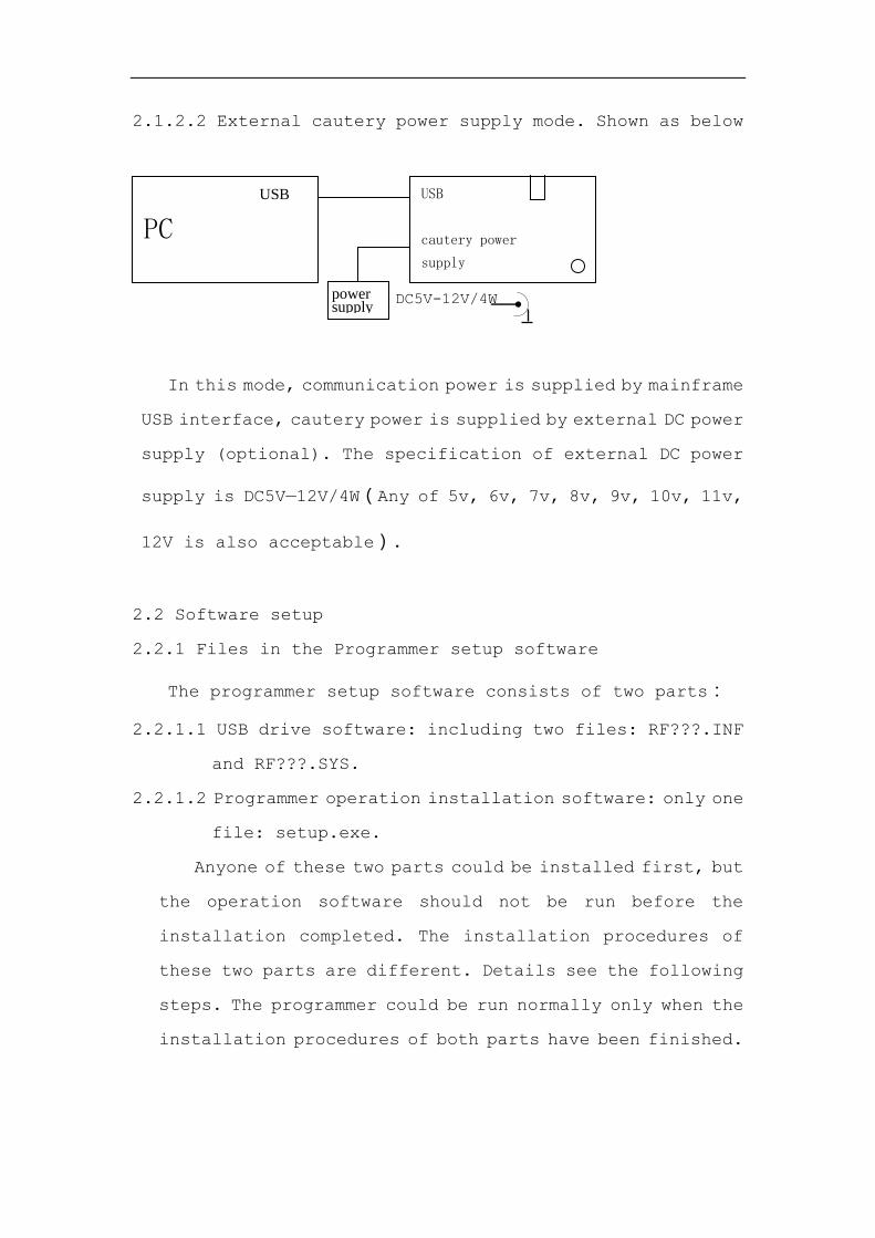
2.1.2.2 External cautery power supply mode. Shown as below
DC5V-12V/4W
In this mode, communication power is supplied by mainframe
USB interface, cautery power is supplied by external DC power
supply (optional). The specification of external DC power
supply is DC5V—12V/4W(Any of 5v, 6v, 7v, 8v, 9v, 10v, 11v,
12V is also acceptable).
2.2 Software setup
2.2.1 Files in the Programmer setup software
The programmer setup software consists of two parts:
2.2.1.1 USB drive software: including two files: RF???.INF
and RF???.SYS.
2.2.1.2 Programmer operation installation software: only one
file: setup.exe.
Anyone of these two parts could be installed first, but
the operation software should not be run before the
installation completed. The installation procedures of
these two parts are different. Details see the following
steps. The programmer could be run normally only when the
installation procedures of both parts have been finished.
USB
PC
USB
cautery power
supply
power supply

2.2.2 Installation of USB drive software
For this installation, there are two instances with a little
difference between them.
2.2.2.1 Initial installation of "device drive" program to the
object computer
(1) Connect two cables with the programmer power off.
(2) Power on the programmer. The operation system will
give the message that a new hardware is found, and
require to install the device drive program.
(3) Follow the wizard to install the USB drive program
named RF???.INF. (RF???.SYS will be automatically
processed by the operation system. Normally manual
intervention is not necessary)
2.2.2.2 Reinstall or upgrade "device drive" program
("device drive" program is not necessary to be updated
whenever software upgraded. If everything is normal, only the
"operation software" updating is needed.)
If "device drive" program of the programmer has been
installed before, when power on the programmer, the operation
system will neither give the message of finding a new hardware,
nor require device drive program installation. Modifying or
upgrading of the "device drive" program should be carried out
by "control panel" of operation system.
(1) Connect 2 cables with the programmer power off. Then
power on the programmer.
(2) Access to the window of device manager by click on
START -> CONTROL PANEL -> SYSTEM -> DEVICE MANAGER.
(3) In the window of "device manager", click on "+" before
relative items, find the device named RF??? and select
it.
(4) Update this device drive program. (Note: Select
"specified location of the drive program" and point
to real RF???.INF drive program installation file.
Sometimes the operation system will reinstall copy of
the old drive program instead of updating this device
drive program. Details please read the file
"installation instruction.txt" in the compact disc.
2.2.3 Installation of the programmer operation software
Installation of the operation software is easier. Just run
"setup.exe" and follow the displayed messages until finish.
To upgrade the operation software, just perform new
installation. It is not necessary to uninstall the old software.
2.2.4 Software uninstalling
Uninstall only the operation software with the "device
drive" program kept. It will be performed by "control panel"
of the operation system.
Chapter 3 Main Menu & Main Functions
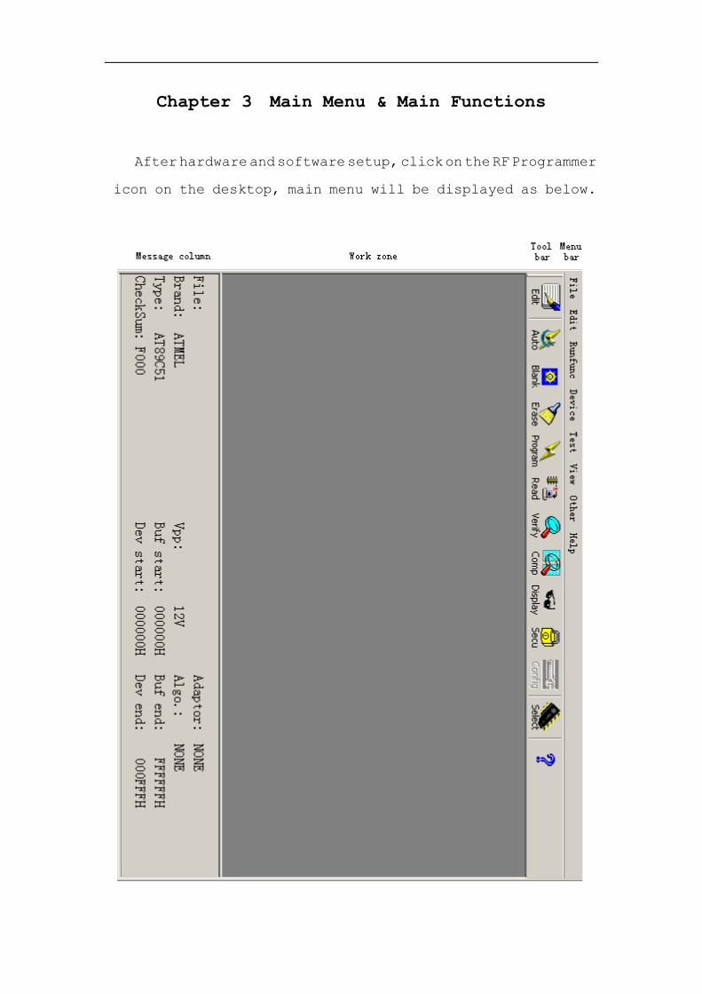
After hardware and software setup, click on the RF Programmer
icon on the desktop, main menu will be displayed as below.

3.1 Main menu introduction
3.1.1 Function items in menu bar
Click on function items in menu bar, corresponding
pull-down menu will popup. Operations of the function item
could be found in the pull-down menu.
3.1.2 Toolbar
For user’s convenience, some frequently used operations
in the pull-down menu are arranged in the toolbar as icons.
To perform an operation, just click on the right icon directly.
The tool icons are dynamic. If one icon turns grey, the function
is not available for selected device.
3.1.3 Work zone
When operations are been doing, all the edit, dialog, view,
run and finish messages are all displayed in the work zone.
3.1.4 Message column
In the message column, displays relative current messages,
for example, loaded file name, brand and type of current selected
device, accumulative checksum of data in buffer, programming
voltage and adaptor type of current selected device, start
and end addresses of current buffer, start and end addresses
of current device, programming mode of EPROM device.
3.1.5 Prompt case
When the mouse points at an operation, the followed prompt
case will give interpretative messages.

3.2 File function item
Click on File item in the menu, pull-down menu of File
function will popup, including three operations: load file,
save file, exit.
3.2.1 Load file
This operation is to load file from disk to buffer for
programming, modifying and viewing. Load File could be operated
after chip type selected.
Click on Load File, pops up menu of file format selection
with seven options: Binary, Intel Hex, Motorola Hex, EMC CDS,
Holtek OTP, POF, JEDEC, in which JEDEC is only for logic array
device.
Click on the needed format, pops up window of load start
address and load mode selection as below.
In this window, need to fill in two start addresses (default
as 000000, not necessary to change normally) and select file
load mode (default as Normal), then click on OK.
When loading file, file data started from “File Start”
will be loaded into buffer started from “buf start”.
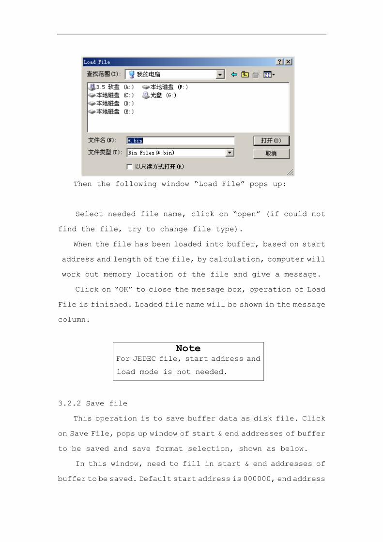
Then the following window “Load File” pops up:
Select needed file name, click on “open” (if could not
find the file, try to change file type).
When the file has been loaded into buffer, based on start
address and length of the file, by calculation, computer will
work out memory location of the file and give a message.
Click on “OK” to close the message box, operation of Load
File is finished. Loaded file name will be shown in the message
column.
Note For JEDEC file, start address and
load mode is not needed.
3.2.2 Save file
This operation is to save buffer data as disk file. Click
on Save File, pops up window of start & end addresses of buffer
to be saved and save format selection, shown as below.
In this window, need to fill in start & end addresses of
buffer to be saved. Default start address is 000000, end address

is the start address + capacity of current device, not necessary
to change normally. After select file save mode, click on OK.
Then the window of Save File pops up as below:
In this window, after select the needed directory and file
name to save, click on “save”, operation of Save File is
finished.
Note
To save JEDEC file, start & end addresses and
file format is not needed.
3.2.3 Exit
Click on “exit”, system will exit the menu.
3.3 Edit function item
Click on Edit item in the menu, pull-down menu of Edit
function will popup, including four operations: edit buffer,
fill buffer, clear buffer, change address.
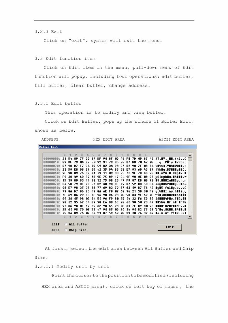
3.3.1 Edit buffer
This operation is to modify and view buffer.
Click on Edit Buffer, pops up the window of Buffer Edit,
shown as below.
ADDRESS HEX EDIT AREA ASCII EDIT AREA
At first, select the edit area between All Buffer and Chip
Size.
3.3.1.1 Modify unit by unit
Point the cursor to the position to be modified (including
HEX area and ASCII area), click on left key of mouse, the

cursor twinkles. At this position, HEX number or ASCII
character could be input by keyboard.
3.3.1.2 Edit function menu
In the edit window, click on right key of mouse, pops
up Edit Function Menu with multi-options.
3.3.1.3 Block modification of specified area
Point the cursor to start position of specified area
(HEX area), keep pressing left key of mouse, drag to end
position of specified area, release left key, then the
selected area will be highlighted. Alternatively, click on
right key of mouse, select specified area by option Select
Block. When the area specified, click on right key of mouse,
pops up options of Cut, Copy, Delete, Paste, and Fill, which
could be used to perform block modification of specified
area.
3.3.2 Fill buffer
This operation is to fill the entire buffer with HEX number
FFH.
3.3.3 Clear buffer
This operation is to fill the entire buffer with HEX number
00H.
3.3.4 Change address
This operation is to set start & end addresses of buffer
and start address of the device. Default start & end addresses
of buffer are 000000 and 0FFFFF respectively, default start
address of the device is 000000, not necessary to change
normally.

3.4 Device function item
Click on Device item in the menu, pops up a pull-down menu,
including device selection operation. Click on Select Device,
pops up the window of Select, shown as below:
At first, select and click before needed type among options
EPROM, SPROM, EEPROM, PLD, and MPU/MCU.
Then select the vendor. In the vendor column, find the
right vendor and click.
The next step is to select the device. In the device column,
find the right type and click.
When these steps finished, click on OK to exit Device
Selection. The selected device type, as well as relative
information, will be shown as current type in message column
of main menu.
3.5 Runfunc function item
Click on Runfunc item in the menu, pops up a pull-down menu
of programming function with different options depending on
different selected current device types, including auto, erase,
blank, program, read, verify, compare, ID code, configuration,
display, encryption, lock, change algorithm, etc.
3.5.1 Erase
This operation is to delete content of electrical erasable
device to blank it.
Click on Erase, pops up the window of Erase. Mount the device
to be erased correctly, click on OK to start erase operation.
3.5.2 Blank
This operation is to check if the device is blank.
Click on Blank option, pops up the window of Blank Check.
Mount the device to be checked correctly, click on OK to start
blank checking. If the device is blank, gives the message “Blank
check complete”, or else gives the message “Error at ××××××H!”
(××××××H is address of the first error unit).
3.5.3 Verify
This operation is to verify if content of the device is
identical with that of the buffer.
Click on Verify option, pops up the window of Verify. Mount
the device to be verified correctly, click on OK to start.
If no error found, gives the message “Verify complete!”, or
else gives the message “Error at ××××××H! Device: ×× Buffer:
××” (××××××H is address of the first error unit, Device: ××
Buffer: ×× represents content of device and of buffer at this

address respectively).
3.5.4 Compare
The operation is to compare content of the device with that
of the buffer unit by unit, and display all the different units.
Click on Compare option, pops up the window of Compare.
Mount the device to be compared correctly, click on OK to start.
If no difference, gives the message “Compare complete!”, or
else pops up the window of Compare Device, as shown below,
displays all the error units.
In this window, correct data in buffer and error in the
chip will be displayed alternatively, and marked in red and
blue color respectively. Data in red show error in the chip,
data in blue are correct data in buffer, other data in grey
represent identical comparing results.
Fixed mode as “buffer” or “chip” could be selected, to
display “correct data in buffer” or “error in the chip”. Here
the error data will still be marked in red and blue color
respectively.

3.5.5 Read
This operation is to read content of the device into buffer.
Click on Read option, pops up the window of Read. Mount
the device to be read correctly, click on OK to start.
3.5.6 Display
This operation is to display content of the device on screen
for viewing. Click on Display option, pops up the window of
Display Device, shown as below.
Drag the vertical scroll bar to view the display up and
down.
Note
If read content is important, when reading is finished,
suggest exit the window of Read, verify read data by
Verify function to ensure read data be correct.
Note
The displayed device content is just
shown on the screen, not in buffer.
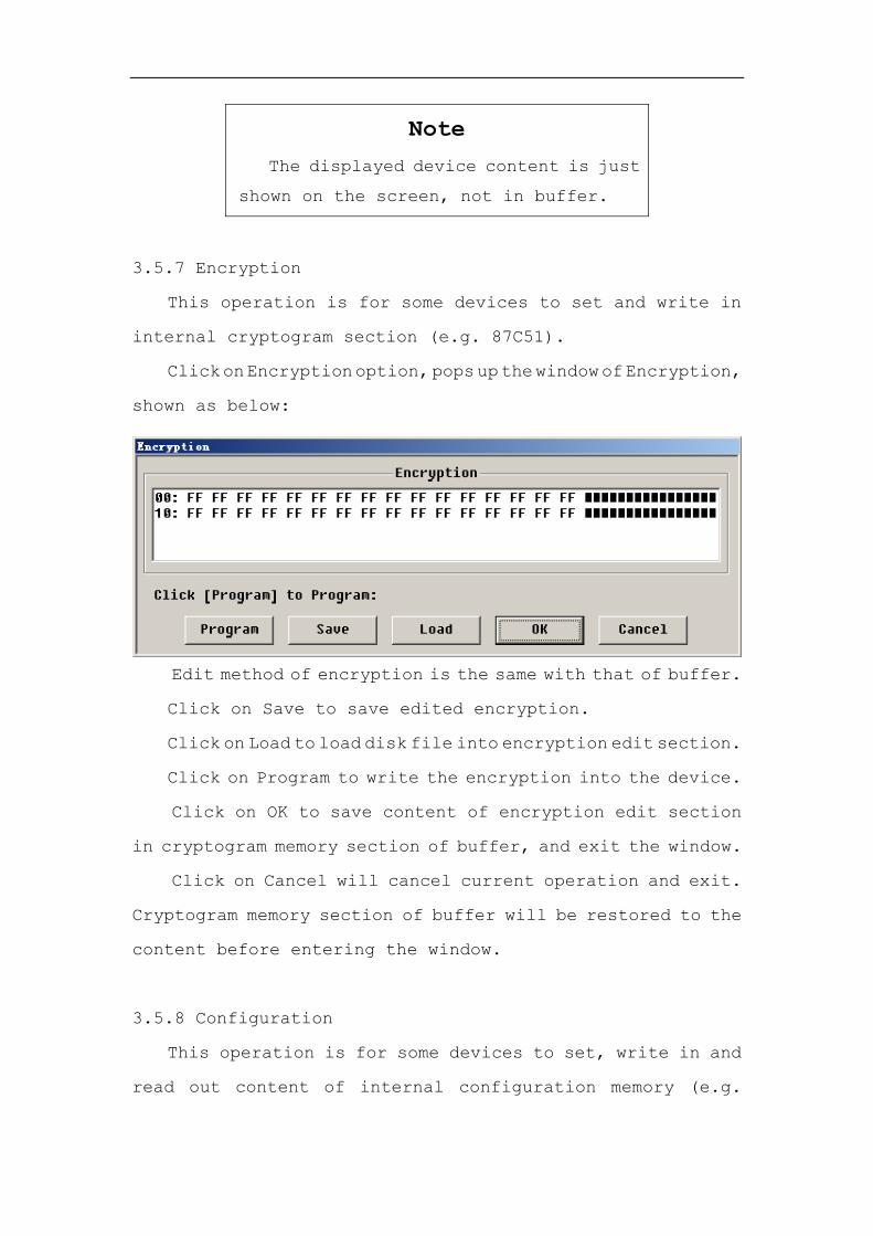
3.5.7 Encryption
This operation is for some devices to set and write in
internal cryptogram section (e.g. 87C51).
Click on Encryption option, pops up the window of Encryption,
shown as below:
Edit method of encryption is the same with that of buffer.
Click on Save to save edited encryption.
Click on Load to load disk file into encryption edit section.
Click on Program to write the encryption into the device.
Click on OK to save content of encryption edit section
in cryptogram memory section of buffer, and exit the window.
Click on Cancel will cancel current operation and exit.
Cryptogram memory section of buffer will be restored to the
content before entering the window.
3.5.8 Configuration
This operation is for some devices to set, write in and
read out content of internal configuration memory (e.g.
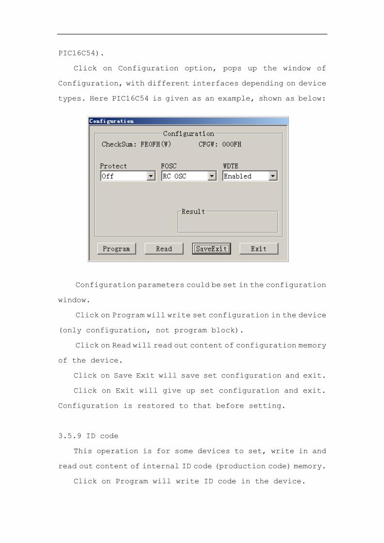
PIC16C54).
Click on Configuration option, pops up the window of
Configuration, with different interfaces depending on device
types. Here PIC16C54 is given as an example, shown as below:
Configuration parameters could be set in the configuration
window.
Click on Program will write set configuration in the device
(only configuration, not program block).
Click on Read will read out content of configuration memory
of the device.
Click on Save Exit will save set configuration and exit.
Click on Exit will give up set configuration and exit.
Configuration is restored to that before setting.
3.5.9 ID code
This operation is for some devices to set, write in and
read out content of internal ID code (production code) memory.
Click on Program will write ID code in the device.
Click on Read will load ID code from the device.
Click on Exit will save current ID code and exit.
3.5.10 Security
This operation is to set read/write prohibition(i.e.
protection) for content in internal memory of single chip device.
For some devices, this memory protection is implemented in
Configuration.
Click on Security option, pops up the window of Security.
Set protection level in the window.
Click on OK to start.
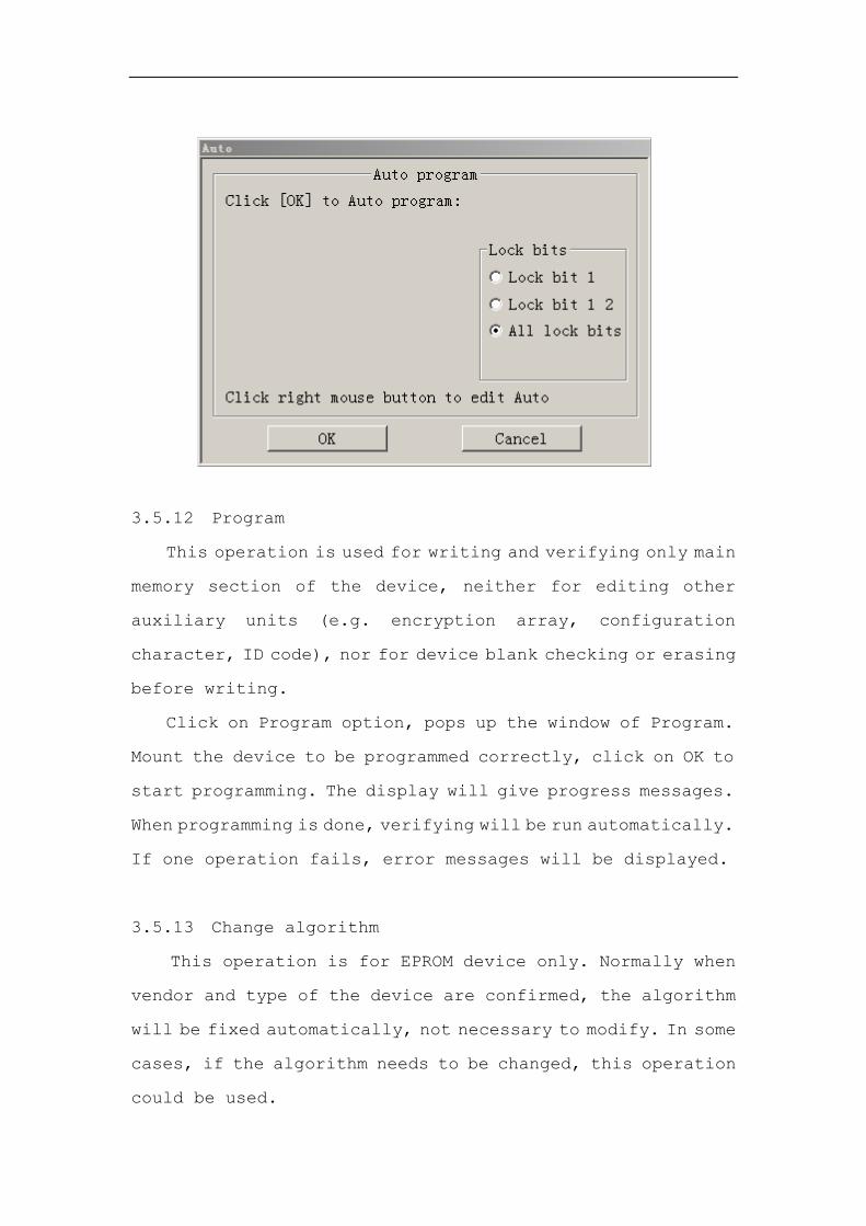
3.5.11 Auto
This operation will automatically carry out (erase), blank,
program, verify, (encryption), (ID code), (configuration),
(security) in sequence, to finish all writing process for the
device.
Note: operations in brackets are available only for devices
with corresponding functions.
Click on Auto option, pops up the window of Auto program,
taking AT89C51 as an example, shown as below:
Mount the device to be programmed correctly, select needed
lock bits.
Click on OK to start auto program. The display will give
messages of current operation and progress. The next operation
will be run automatically once the previous one is done until
all completed. If one operation fails, error message will be
displayed, the next operation will be stopped.
3.5.12 Program
This operation is used for writing and verifying only main
memory section of the device, neither for editing other
auxiliary units (e.g. encryption array, configuration
character, ID code), nor for device blank checking or erasing
before writing.
Click on Program option, pops up the window of Program.
Mount the device to be programmed correctly, click on OK to
start programming. The display will give progress messages.
When programming is done, verifying will be run automatically.
If one operation fails, error messages will be displayed.
3.5.13 Change algorithm
This operation is for EPROM device only. Normally when
vendor and type of the device are confirmed, the algorithm
will be fixed automatically, not necessary to modify. In some
cases, if the algorithm needs to be changed, this operation
could be used.

Click on Change Algorithm option, pops up the window of
Change Algorithm, shown as below.
Select needed algorithm in the window, click on OK to exit.
3.6 Test function item
Click on Test item in the menu, pops up a pull-down menu
of test function, including Logic IC Test, Static RAM Test,
Peripheral IC Test, etc.
3.6.1 Logic IC Test
This operation is to test IC of TTL74/54 series, CMOS40/45
series, and search for unknown IC model of these series.
NOTE
For EPROM devices programming voltage
unknown, when select algorithm, recommend
to try from low voltage.

Click on Logic IC Test option, pops up the window of Logic
ICs Test, shown as below.
At first, select device series to be tested. Select the
right series in the IC series column and click.
Then select the chip. In the chip column, find the right
chip type and click.
Now mount the device to be tested correctly, click on Test
to perform single test. Test result will be displayed when
test finished. Click on Looptest to perform multiple tests.
Click on Cancel to stop looptest.
When search for unknown type, click on Search respectively
by selecting device series as TTL74, CMOS4000, CMOS4500 in
sequence. If matched types are found, displays the one or more
relative types.
Searching for unknown type could not be performed of
multi-series.
If multiple matched types are found, means these types of
devices are of same logic functions, yet circuit characters
could be different.
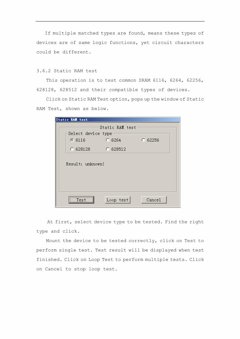
3.6.2 Static RAM test
This operation is to test common SRAM 6116, 6264, 62256,
628128, 628512 and their compatible types of devices.
Click on Static RAM Test option, pops up the window of Static
RAM Test, shown as below.
At first, select device type to be tested. Find the right
type and click.
Mount the device to be tested correctly, click on Test to
perform single test. Test result will be displayed when test
finished. Click on Loop Test to perform multiple tests. Click
on Cancel to stop loop test.

Chapter 4 Other Function Item
(not for RF-910 user)
Other function item involves some additional functions
provided by RF series programmer, including operations to
convert JEDEC of 16V8, 20V8 into logic expression, to read
secured IC of GAL16V8/A/B, GAL20V8/A/B, PALCE16V8H, PALCE20V8H,
to secure AT89C51/52/1051/2051 unrecoverable by RF2148 and
RF3148.
4.1 JED to logic
This operation is to convert JEDEC of 16V8, 20V8, 22V10
to logic expression for analysis and modification.
Firstly select device type. Load the JEDEC file into buffer,
click on JED To Logic option, pops up the window of JED To
Logic, shown as below.
In which * is logic AND, + is logic OR, / is logic NO, OXX.OE

is output hi-impedance control, OXX is output of flip-latch
type.
Click on Save to save the logic expression as disk file.
4.2 Read secured IC
This operation is to read out secured content of some devices
by special method.
At first, select device type to be read. Click on Read
Secured IC option, pops up the window of Read Secured IC. Mount
the device to be read correctly, click on OK to start reading.
If succeeds, gives message “Complete! The IC data can be read
out”. Otherwise gives message of failure.
Note:
(1) For GAL device itself, it is still secured after this
reading operation. Its content has been read into buffer.
(2) For PALCE16V8H/20V8H, at whiles, some times of reading
are needed (less than 10 times). After reading, the device
is unsecured. Its content could be loaded into buffer by Read
operation. It is recommended that, when the first reading is
finished, read its content and save, then read again the
unsecured device. Compare two reading results. If they are
the same, the result is correct.
4.3 Special protect (OTP)
This operation is to perform special processing for
microchip unit AT89C5X/X051, to enhance its security degree.
Firstly select right type of the device to be protected.
Click on Special Protect option, pops up the window of Special
Protect.

Without adaptor: (not available for RF3148)
To perform OTP security for AT89C5X, adaptor is not necessary.
Place the programmed and 3-level secured chip on lock seat
of the programmer in reverse direction (notch of chip away
from the lock seat handle), click on OK to start.
Note: The chip must be 3-level secured!!! The OTP secured
chip could not be erased and modified again! OTP secured chip
will not kill data bus, have no influence on extending function.
With adaptor:
If K51 security adaptor (optional) is used, it is possible
to perform OTP security for AT89C5X, as well as to kill idle
pins of data line P0.0—P0.7 of AT89C5X or P1.2—P1.7 of AT89CX051,
to enhance security degree. Killed pins could not be used
normally.
The way to use K51 security adaptor is to put it on mainframe
of the programmer. There are two kinds of security operations:
(1) OTP security
This is applicable to only AT89C5X. Connect jumpers on the
circuit board of K51 adaptor according to software prompts,
place the programmed and 3-level secured chip on lock seat
of K51 adaptor normally, click on OK to start.
(2) Data line killing. Place the programmed chip
AT89C5X/X051 on lock seat of K51 adaptor normally, select data
line to be killed among P0.0—P0.7 of AT89C5X or P1.2—P1.7 of
AT89CX051 by jumpers according to software prompts, click on
OK to start.
Chapter 5 Precaution
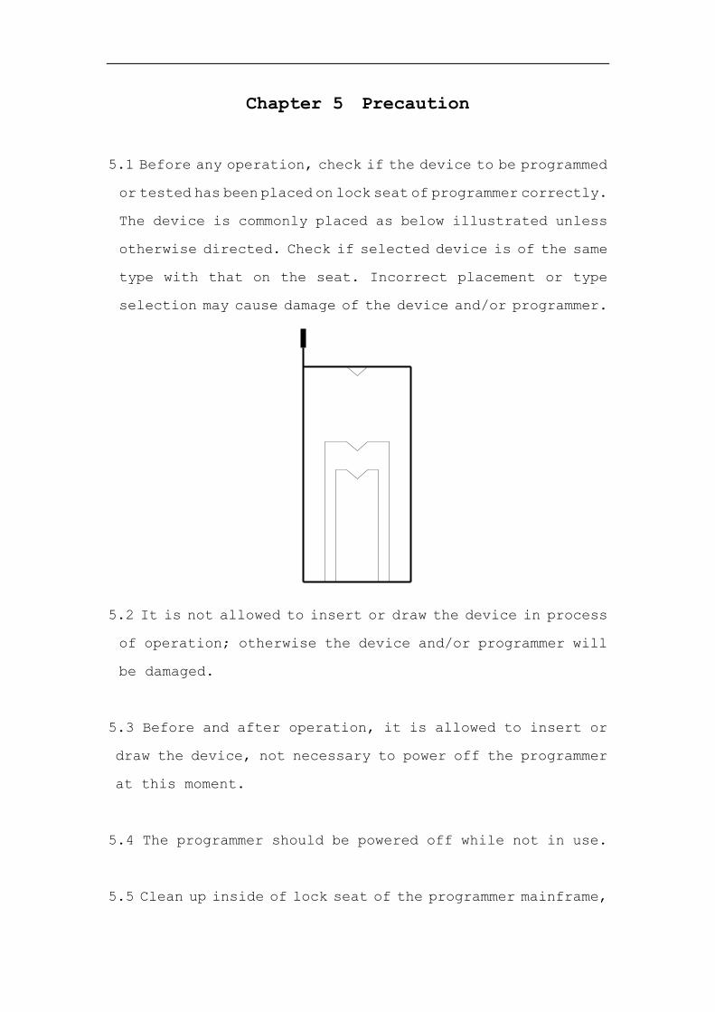
5.1 Before any operation, check if the device to be programmed
or tested has been placed on lock seat of programmer correctly.
The device is commonly placed as below illustrated unless
otherwise directed. Check if selected device is of the same
type with that on the seat. Incorrect placement or type
selection may cause damage of the device and/or programmer.
5.2 It is not allowed to insert or draw the device in process
of operation; otherwise the device and/or programmer will
be damaged.
5.3 Before and after operation, it is allowed to insert or
draw the device, not necessary to power off the programmer
at this moment.
5.4 The programmer should be powered off while not in use.
5.5 Clean up inside of lock seat of the programmer mainframe,

lest fault device writing occur caused by bad contact due
to dusty sediment.

Introduction of User Vector Test Function
The user could define the test vector of a device to test
it.
In menu of Windows version software, click on Test. In the
popup pull-down menu, click on User Vector Test to access
interface of Vector Test.
A. Create a test vector table of the new device (74LS138 as
an example)
1. Click on File, click on New, pops up the window of Pin
Selection. Since 74LS138 is of 16 pins, select 16Pin,
click on OK.
2. Now the vector edit section appears. Edit the test
vector table according to need. Vector table of 74LS138
is as follows:
0 0 0 0 0 0 0 0 0 1 1 1 1 1 1 1 (pin number)
1 2 3 4 5 6 7 8 9 0 1 2 3 4 5 6
V001 0 0 0 0 0 1 H G H H H H H H L E
V002 1 0 0 N N N H G H H H H H L H E
V003 0 1 0 N N N H G H H H H L H H E
V004 1 1 0 N N N H G H H H L H H H E
V005 0 0 1 N N N H G H H L H H H H E
V006 1 0 1 N N N H G H L H H H H H E
V007 0 1 1 N N N H G L H H H H H H E
V008 1 1 1 N N N L G H H H H H H H E
In which:
0:represents that the programmer supplies low voltage to tested
device
1:represents that the programmer supplies high voltage to tested
device
L:represents that the device outputs low voltage
H:represents that the device outputs low voltage
N:represents that keeps previous state
X:represents that this pin is not involved in the test
E:represents 5V power supply
G:represents earthing
3.Click on Edit to select tools such as Cut, Copy, Paste, Delete,

Insert, and Append.
4.Click on File, select Save or Save As to save the edited vector
table as a file.
B. Test
1. When the test vector table is edited, place the device to be
tested on lock seat of programmer.
2. Click on Test or T to implement single test.
3. Click on Loop Test or L to implement continuous test.
4. If any error found during test, the error message window will
pop up to compare the vector table with test result.
C. Remarks
1. Not all pins could supply 5V electrical source (E) or ground
(G). If a pin is not able to be input E or G during vector editing,
that means this pin could not supply 5V or ground.
2. Pins not involved in test (X) are drawn up to 5V by 4K resistance
inside the programmer.