the unijunction transistor (ujt) _ thyristors
TRANSCRIPT

Unijunction transistor: Although a unijunction transistor is not a thyristor, this devicecan trigger larger thyristors with a pulse at base B1. A unijunction transistor is composed ofa bar of N-type silicon having a P-type connection in the middle. See Figure below(a). Theconnections at the ends of the bar are known as bases B1 and B2; the P-type mid-point isthe emitter. With the emitter disconnected, the total resistance RBBO, a datasheet item, isthe sum of RB1 and RB2 as shown in Figure below(b). RBBO ranges from 4-12kΩ for differentdevice types. The intrinsic standoff ratio η is the ratio of RB1 to RBBO. It varies from 0.4 to0.8 for different devices. The schematic symbol is Figure below(c)
Unijunction transistor: (a) Construction, (b) Model, (c) Symbol
The Unijunction emitter current vs voltage characteristic curve (Figure below(a) ) showsthat as VE increases, current IE increases up IP at the peak point. Beyond the peak point,current increases as voltage decreases in the negative resistance region. The voltagereaches a minimum at the valley point. The resistance of RB1, the saturation resistance islowest at the valley point.
IP and IV, are datasheet parameters; For a 2n2647, IP and IV are 2µA and 4mA,respectively. [AMS] VP is the voltage drop across RB1 plus a 0.7V diode drop; see Figurebelow(b). VV is estimated to be approximately 10% of VBB.
The Unijunction Transistor (UJT) : Thyristors file:///C:/Documents and Settings/student/My Documents/Downloads/The...
1 of 6 17/03/2014 6:41 PM

Unijunction transistor: (a) emitter characteristic curve, (b) model for VP .
The relaxation oscillator in Figure below is an application of the unijunction oscillator. RE
charges CE until the peak point. The unijunction emitter terminal has no effect on thecapacitor until this point is reached. Once the capacitor voltage, VE, reaches the peakvoltage point VP, the lowered emitter-base1 E-B1 resistance quickly discharges thecapacitor. Once the capacitor discharges below the valley point VV, the E-RB1 resistancereverts back to high resistance, and the capacitor is free to charge again.
Unijunction transistor relaxation oscillator and waveforms. Oscillator drives SCR.
During capacitor discharge through the E-B1 saturation resistance, a pulse may be seen onthe external B1 and B2 load resistors, Figure above. The load resistor at B1 needs to below to not affect the discharge time. The external resistor at B2 is optional. It may bereplaced by a short circuit. The approximate frequency is given by 1/f = T = RC. A moreaccurate expression for frequency is given in Figure above.
The charging resistor RE must fall within certain limits. It must be small enough to allow IPto flow based on the VBB supply less VP. It must be large enough to supply IV based on theVBB supply less VV. [MHW] The equations and an example for a 2n2647:
Programmable Unijunction Transistor (PUT): Although the unijunction transistor islisted as obsolete (read expensive if obtainable), the programmable unijunction transistoris alive and well. It is inexpensive and in production. Though it serves a function similar tothe unijunction transistor, the PUT is a three terminal thyristor. The PUT shares thefour-layer structure typical of thyristors shown in Figure below. Note that the gate, anN-type layer near the anode, is known as an “anode gate”. Moreover, the gate lead on theschematic symbol is attached to the anode end of the symbol.
The Unijunction Transistor (UJT) : Thyristors file:///C:/Documents and Settings/student/My Documents/Downloads/The...
2 of 6 17/03/2014 6:41 PM

Programmable unijunction transistor: Characteristic curve, internal construction, schematicsymbol.
The characteristic curve for the programmable unijunction transistor in Figure above issimilar to that of the unijunction transistor. This is a plot of anode current IA versus anodevoltage VA. The gate lead voltage sets, programs, the peak anode voltage VP. As anodecurrent inceases, voltage increases up to the peak point. Thereafter, increasing currentresults in decreasing voltage, down to the valley point.
The PUT equivalent of the unijunction transistor is shown in Figure below. External PUTresistors R1 and R2 replace unijunction transistor internal resistors RB1 and RB2,respectively. These resistors allow the calculation of the intrinsic standoff ratio η.
PUT equivalent of unijunction transistor
Figure below shows the PUT version of the unijunction relaxation oscillator Figure previous.Resistor R charges the capacitor until the peak point, Figure previous, then heavyconduction moves the operating point down the negative resistance slope to the valleypoint. A current spike flows through the cathode during capacitor discharge, developing avoltage spike across the cathode resistors. After capacitor discharge, the operating pointresets back to the slope up to the peak point.
The Unijunction Transistor (UJT) : Thyristors file:///C:/Documents and Settings/student/My Documents/Downloads/The...
3 of 6 17/03/2014 6:41 PM

PUT relaxation oscillator
Problem: What is the range of suitable values for R in Figure above, a relaxationoscillator? The charging resistor must be small enough to supply enough current to raisethe anode to VP the peak point (Figure previous) while charging the capacitor. Once VP isreached, anode voltage decreases as current increases (negative resistance), which movesthe operating point to the valley. It is the job of the capacitor to supply the valley currentIV. Once it is discharged, the operating point resets back to the upward slope to the peakpoint. The resistor must be large enough so that it will never supply the high valley currentIP. If the charging resistor ever could supply that much current, the resistor would supplythe valley current after the capacitor was discharged and the operating point would neverreset back to the high resistance condition to the left of the peak point.
We select the same VBB=10V used for the unijunction transistor example. We select valuesof R1 and R2 so that η is about 2/3. We calculate η and VS. The parallel equivalent of R1,R2 is RG, which is only used to make selections from Table below. Along with VS=10, theclosest value to our 6.3, we find VT=0.6V, in Table below and calculate VP.
We also find IP and IV, the peak and valley currents, respectively in Table below. We stillneed VV, the valley voltage. We used 10% of VBB= 1V, in the previous unijunction example.Consulting the datasheet, we find the forward voltage VF=0.8V at IF=50mA. The valleycurrent IV=70µA is much less than IF=50mA. Therefore, VV must be less than VF=0.8V.How much less? To be safe we set VV=0V. This will raise the lower limit on the resistorrange a little.
The Unijunction Transistor (UJT) : Thyristors file:///C:/Documents and Settings/student/My Documents/Downloads/The...
4 of 6 17/03/2014 6:41 PM
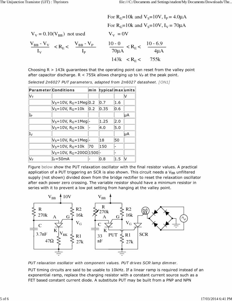
Choosing R > 143k guarantees that the operating point can reset from the valley pointafter capacitor discharge. R < 755k allows charging up to VP at the peak point.
Selected 2n6027 PUT parameters, adapted from 2n6027 datasheet. [ON1]
Parameter Conditions min typical max units
VT V
VS=10V, RG=1Meg 0.2 0.7 1.6
VS=10V, RG=10k 0.2 0.35 0.6
IP µA
VS=10V, RG=1Meg - 1.25 2.0
VS=10V, RG=10k - 4.0 5.0
IV µA
VS=10V, RG=1Meg - 18 50
VS=10V, RG=10k 70 150 -
VS=10V, RG=200Ω 1500 - -
VF IF=50mA - 0.8 1.5 V
Figure below show the PUT relaxation oscillator with the final resistor values. A practicalapplication of a PUT triggering an SCR is also shown. This circuit needs a VBB unfilteredsupply (not shown) divided down from the bridge rectifier to reset the relaxation oscillatorafter each power zero crossing. The variable resistor should have a minimum resistor inseries with it to prevent a low pot setting from hanging at the valley point.
PUT relaxation oscillator with component values. PUT drives SCR lamp dimmer.
PUT timing circuits are said to be usable to 10kHz. If a linear ramp is required instead of anexponential ramp, replace the charging resistor with a constant current source such as aFET based constant current diode. A substitute PUT may be built from a PNP and NPN
The Unijunction Transistor (UJT) : Thyristors file:///C:/Documents and Settings/student/My Documents/Downloads/The...
5 of 6 17/03/2014 6:41 PM

silicon transistor as shown for the SCS equivalent circuit in Figure below by omitting thecathode gate and using the anode gate.
REVIEW:A unijunction transistor consists of two bases (B1, B2) attached to a resistive bar ofsilicon, and an emitter in the center. The E-B1 junction has negative resistanceproperties; it can switch between high and low resistance.A PUT (programmable unijunction transistor) is a 3-terminal 4-layer thyristor actinglike a unijunction transistor. An external resistor network “programs” η.The intrinsic standoff ratio is η=R1/(R1+R2) for a PUT; substitute RB1 and RB2,respectively, for a unijunction transistor. The trigger voltage is determined by η.Unijunction transistors and programmable unijunction transistors are applied tooscillators, timing circuits, and thyristor triggering.
Related Links
Worksheet: Opamp oscillator circuitsWorksheet: ThyristorsWorksheet: Thyristor application circuitsWorksheet: Oscillator circuitsWorksheet: JFET amplifiersForum: Project: PIC 4-Digit 99 Minute TimerForum: Capacitive discharge welder - Uncertainties charging with a MOSFET + opamp systemForum: E-book Correction typo UJT sectionForum: Spice modeling a PUT oscillatorForum: Capacitors
RS Components Australiaaustralia.rs-online.comGet your products within 24 hours Order Online at RS Now!
The Unijunction Transistor (UJT) : Thyristors file:///C:/Documents and Settings/student/My Documents/Downloads/The...
6 of 6 17/03/2014 6:41 PM