theoretical and experimental investigations on snubber circuits · pdf file ·...
TRANSCRIPT

Theoretical and Experimental Investigations on Snubber Circuits for High Voltage Valves of
FACTS-Equipment for Over-voltage Protection
Submitted to
The Faculty of Engineering at the Friedrich-Alexander University of
Erlangen-Nuremberg
to obtain the degree
DOKTOR-INGENIEUR
presented by
Jamal Alnasseir
Erlangen 2007

As dissertation approved by The Faculty of Engineering Science of the Friedrich-Alexander University of Erlangen-Nuremberg
Day of submission: 26.03.2007
Day of examination: 31.05.2007
Dean: Prof. Dr.-Ing. A. Leipertz
Examiners: Prof. Dr.-Ing. G. Herold
Prof. Dr.-Ing. J. Petzoldt

Theoretische und experimentelle Untersuchung der Schutzbeschaltung von
Hochspannungsventilen für FACTS-Anlagen
Der Technischen Fakultät
der Friedrich-Alexander Universität Erlangen-Nürnberg
zur Erlangung des Grades
DOKTOR-INGENIEUR
vorgelegt von
Jamal Alnasseir
Erlangen 2007

Als Dissertation genehmigt von der Technischen Fakultät der Friedrich-Alexander-Universität Erlangen-Nürnberg
Tag der Einreichung: 26.03.2007
Tag der Promotion: 31.05.2007
Dekan: Prof. Dr.-Ing. A. Leipertz
Berichterstatter: Prof. Dr.-Ing. G. Herold
Prof. Dr.-Ing. J. Petzoldt

Preface
Preface
This dissertation follows from my research work done as a doctoral student at the Institute for
Electrical Power System in the Friedrich-Alexander University of Erlangen-Nuremberg, Germany.
I would like to express my deep thankfulness to my supervisor Univ.-Prof. Dr.-Ing. habil. Gerhard
Herold for giving me the chance to this interesting research area, for his invaluable friendship, for his
completely trusts with me, and for the excellent working conditions.
I would like to thank Prof. Dr.-Ing. habil J. Petzoldt, TU Ilmenau, for being the external examiner
of my dissertation. A warm thanks also to Prof. Dr.-Ing. J. Schlücker for being one of my examiners.
My sincere thanks go to Prof. Dr.-Ing A. Hamzeh for his help and support.
I want to thank all my colleagues at my institute, Dr.-Ing Mayer, Prof. Dr-Ing. Jäger, Mrs. Biegel,
Mrs Gambel, Mrs. Strößner, Dipl.-Ing. Braisch, Dr.-Ing. Gawlik, Dipl.-Ing. Ebner, Dipl.-Ing.
Rubenbauer, Dipl.-Ing. Keil, Dipl.-Ing. Ramold, Dipl.-Ing. Rasic, Dipl.-Ing .Weiland, Dipl.-Ing.
Mladenovic, and Mr. Domhardt, for the unforgettable friendship, for their support, help and consulting
in technology, society and in everyday life. They make me truly enjoy the research work and always
have the feeling as at home.
Warm and special thanks to my colleagues Dr.-Ing Weidl, M.Sc. Gamil, Mr. Leuschner, Mr.
Ruschig and Mr. Oschmann and M.Sc. M. Assem Alrabat. Their support, friendship, discussion and
time for me are much appreciated.
Finally, my sincere gratitude goes to my parents, my sisters and brothers for their ongoing
encouragement and trust. Without their great support, this work would not have been done.

Vorwort
Vorwort
Die vorliegende Dissertation entstand während meines Aufenthaltes als Promotionsstudent am
Lehrstuhl für Elektrische Energieversorgung der Friedrich-Alexander-Universität Erlangen-Nürnberg.
Meinem Doktorvater Herrn Prof. Dr.-Ing. habil G. Herold bin ich Ermöglichung dieser
hochinteressanten Arbeit, seine nette Unterstützung, für sein in mich gesetztes Vertrauen und die
ausgezeichneten Arbeitsbedingungen besonders zu Dank verpflichtet.
Herrn Prof. Dr.-Ing habil J. Petzoldt möchte ich für die Übernahme des Korreferates danken.
Herrn Prof. Dr.-Ing J. Schlücker danke ich herzlich für die Teilnahme an meinem Rigorosum als
fachfremder Prüfer.
Mein aufrichtiger Dank gehört Prof Dr.-Ing A. Hamzeh für seine Hilfe und Unterstützung.
Allen meinen Kolleginnen und Kollegen am Institut, besondere Dr.-Ing Mayer, Prof. Jäger, Fr..
Biegel, Fr. Gambel, Fr. Strößner, Dipl.-Ing. Braisch, Dr.-Ing. Gawlik, Dipl.-Ing. Ebner, Dipl.-Ing.
Rubenbauer, Dipl.-Ing. Keil, Dipl.-Ing. Ramold, Dipl.-Ing. Rasic, Dipl.-Ing. Weiland, Dipl.-Ing.
Mladenovic, and Mr. Domhardt, sei für ihren netten Hilfsstellung, die sehr gute Zusammenarbeit und
das angenehme Arbeitsklima besondere gedankt. Ich habe mich am Lehrstuhl stets wie zuhause
gefühlt.
Darüber hinaus möchte ich mich bei meinen Kollegen Dr.-Ing Weidl, M.Sc. Gamil, Mr.
Leuschner, Mr. Ruschig and Mr. Oschmann and M.Sc. M. Assem Alrabat, für ihre Unterstützung, die
zahlreichen Diskussionen und die aufgewandte Zeit bedanken.
Schließlich geht mein lieber Dank an meine Eltern und meine Geschwister für ihre fortwährende
Ermutigung sowie für ihr Vertrauen. Ohne das hätte ich die Arbeit nicht durchführen können.

Contents
I
Contents
1 Introduction............................................................................................................................................ 1 2 Einleitung............................................................................................................................................... 3 3 Power Semiconductor Devices .............................................................................................................. 6 3.1. Introduction........................................................................................................................................ 6 3.2 Principal high power device characteristics and requirements ........................................................... 8
3.2.1 Voltage and current rating............................................................................................................ 8 3.2.2 Losses and speed of switching ..................................................................................................... 9 3.2.3 Parameter trade-off of the devices ............................................................................................... 9
3.3 Power device material....................................................................................................................... 10 3.4 Perspectives on power devices equipment........................................................................................ 10 3.5 Power diodes..................................................................................................................................... 10
3.5.1 Dynamic characteristics of power switching diodes.................................................................. 11 3.5.2 Reverse-recovery characteristic ................................................................................................. 12 3.5.3 Power diodes types..................................................................................................................... 12
3.6 Insulated Gate Bipolar Transistor (IGBT) ........................................................................................ 13 3.6.1 Switching characteristic of the IGBT ........................................................................................ 15
3.7 Types of high-power thyristor devices.............................................................................................. 15 3.7.1 Thyristors ................................................................................................................................... 16
3.7.1.1 Switching characteristic of thyristor (SCR) ........................................................................ 19 3.7.2 Gate turn-off thyristor (GTO) .................................................................................................... 20
3.7.2.1 Switching characteristics of GTO (turn-on and turn-off process) ...................................... 22 3.7.3 MOS Turn-Off Thyristor ........................................................................................................... 23 3.7.4 Emitter Turn-on Thyristor (ETO) .............................................................................................. 24 3.7.5 Integrated Gate-Commutated Thyristor (GCT and IGCT) ........................................................ 25 3.7.6 MOS-Controlled Thyristor (MCT) ............................................................................................ 26
3.8 Control characteristic of power devices............................................................................................ 27 4 FACTS concept and general system considerations ............................................................................ 29 4.1 Need of transmission interconnection............................................................................................... 29 4.2 Opportunities of FACTS................................................................................................................... 29 4.3 Basic types of FACTS controller ...................................................................................................... 30
4.3.1 Series Controller: ....................................................................................................................... 30 4.3.2 Shunt controller.......................................................................................................................... 31 4.3.3 Combined series-series controller.............................................................................................. 31 4.3.4 Combined series-shunt controller .............................................................................................. 31
4.4 Relative importance of different types of controllers ....................................................................... 31 4.5 Description and definition of FACTS Controllers............................................................................ 34 4.6 Shunt connected controllers .............................................................................................................. 35
4.6.1 Static Synchronous Compensator .............................................................................................. 35 4.6.2 Static Synchronous Generator (SSG)......................................................................................... 36 4.6.3 Battery Energy Storage System (BESS) .................................................................................... 36 4.6.4 Superconducting Magnetic Energy Storage (SMES)................................................................. 36 4.6.5 Static Var Compensator (SVC).................................................................................................. 36 4.6.6 Thyristor Controlled Reactor (TCR).......................................................................................... 37 4.6.7 Thyristor-Switched Reactor (TSR) ............................................................................................ 37

Contents
II
4.6.8 Thyristor Switched Capacitor (TSC) ......................................................................................... 37 4.6.9 Static Var Generator or Absorber (SVG)................................................................................... 37 4.6.10 Static Var System (SVS).......................................................................................................... 37 4.6.11 Thyristor controlled braking Resistor (TCBR) ........................................................................ 37
4.7 Series connected controllers.............................................................................................................. 38 4.7.1 Static Synchronous Series Compensator (SSSC) ...................................................................... 38 4.7.2 Interline Power Flow Controller (IPFC) .................................................................................... 38 4.7.3 Thyristor Controlled Series Capacitor (TCSC).......................................................................... 38 4.7.4 Thyristor-switched Series Capacitor (TSSC)............................................................................. 38 4.7.5 Thyristor-Controlled Series Reactor (TCSR) ............................................................................ 39 4.7.6 Thyristor-switched Series Reactor (TSSR)................................................................................ 40
4.8 Combined Shunt Series Connected Controllers................................................................................ 40 4.8.1 Unified Power Flow Controller (UPFC).................................................................................... 40 4.8.2 Thyristor-Controlled Phase Shifting Transformer (TCPST) ..................................................... 40 4.8.3 Inter-phase Power Controller (IPC) ........................................................................................... 40 4.8.4 Thyristor-Controlled Voltage Limiter (TCVL).......................................................................... 42 4.8.5 Thyristor-Controlled Voltage Regulator (TCVR)...................................................................... 42
4.9 Benefits of FACTS Controllers: ....................................................................................................... 42 5 Voltage-Sourced Converters ................................................................................................................ 43 5.1 Basic concept of Voltage-Sourced Converter (VSC) ....................................................................... 43 5.2 Single-Phase, Voltage Source Converter Circuits ............................................................................ 45 5.3 Output voltage control of single-phase converter ............................................................................. 46
5.3.1 Output voltage control via input voltage regulation .................................................................. 46 5.3.2 Phase control of the converter legs ............................................................................................ 47 5.3.3 Sinusoidal Pulse Width Modulation (SPWM)........................................................................... 47
5.3.3.1 Full-bridge SPWM converter.............................................................................................. 47 5.3.4 Single-phase SPWM converter with Uni-polar Switching Scheme........................................... 48
5.4 Three-phase Voltage-Source Converters .......................................................................................... 49 5.4.1 Converter waveforms with 180° conduction angle.................................................................... 50 5.4.2 Converter waveforms with 120°conduction angle..................................................................... 50
5.5 Output voltage control of thee-phase converters .............................................................................. 50 5.6. Three-level Voltage-Sourced Converter .......................................................................................... 51
5.6.1. Pulse width modulation (PWM) for Three Level Converter .................................................... 52 6 Current-Sourced Converter and Self- and Line-Commutated ............................................................. 55 6.1 Introduction and basic concept of Current-Sourced Converter ........................................................ 55 6.2 Single-phase bridge rectifier ............................................................................................................. 57 6.3 Three-phase bridge rectifier .............................................................................................................. 57 6.4 Phase-controlled AC-DC converters................................................................................................. 58
6.4.1 Single-phase, fully-controlled bridge rectifier ........................................................................... 59 6.5 Three-phase fully controlled bridge converters ................................................................................ 59 6.6 Current-Sourced Converter with turn-off devices ............................................................................ 61 6.7 Current-Sourced versus Voltage-Sourced Converters ...................................................................... 63 7 Snubber Circuits................................................................................................................................... 64 7.1 Introduction....................................................................................................................................... 64 7.2 Function and types of snubber circuits ............................................................................................. 64 7.3 Diode snubber ................................................................................................................................... 65
7.3.1 Capacitive snubber..................................................................................................................... 65 7.3.2 Effect of adding a snubber resistor ............................................................................................ 66

Contents
III
7.4 Snubber circuits for Thyristors ......................................................................................................... 69 7.5 Need for snubber circuits for the transistor....................................................................................... 71 7.6 Turn-off snubber: .............................................................................................................................. 73 7.7 Over-voltage snubber........................................................................................................................ 77 7.8 Turn-on snubber................................................................................................................................ 79 7.9 GTO snubber circuit consideration ................................................................................................... 81 7.10 IGBT Snubber design ..................................................................................................................... 82
7.10.1 Over-voltage causes and their suppression .............................................................................. 82 7.10.2 Over-voltage suppression methods .......................................................................................... 83 7.10.3 Type of IGBT snubber circuits and their features.................................................................... 84
7.10.3.1 RC Snubber circuit ............................................................................................................ 84 7.10.3.2 Charge and discharge RCD Snubber circuit ..................................................................... 85 7.10.3.3 Discharge-suppressing RCD snubber circuit .................................................................... 85 7.10.3.4 C snubber circuit ............................................................................................................... 85 7.10.3.5 RCD snubber circuit.......................................................................................................... 86
7.10.4 Discharge-suppressing RCD snubber circuit design.................................................................... 87 7.10.4.1 A Study of applicability .................................................................................................... 87 7.10.4.2 Calculating the capacitance of the snubber circuit capacitor............................................ 88 7.10.4.3 Calculating snubber resistor.............................................................................................. 88 7.10.4.4 Snubber diode selection .................................................................................................... 88 7.10.4.5 Snubber circuit wiring precautions ................................................................................... 88
8 Simulation results of three-level VSC snubber circuits ....................................................................... 89 8.1 Introduction....................................................................................................................................... 89 8.2 Common snubber circuit for three level inverters ............................................................................ 89 8.3 Double snubber circuit for three level inverters................................................................................ 89 8.4 An optimized snubber design for three level inverters ..................................................................... 91
8.4.1 Performance of the optimized snubber design....................................................................... 97 8.5 Dual-use snubber circuit for three-level inverter .............................................................................. 97 8.6 Dual-inductive snubber circuit for three-level Inverter .................................................................... 98 8.7 Simulation and discussion of the results ........................................................................................... 99
8.7.1 Description of the PWM in Matlab®/SimulinkTM................................................................... 100 8.7.2 Comparison of the proposed double snubber configuration and the common snubber circuit 102
8.7.2.1 Conclusion remarks........................................................................................................... 108 8.7.3 Comparing the common and the optimized snubber design .................................................... 109 8.7.4 Comparison of the common and the dual-use snubber circuits for different values for CS-D .. 116 8.7.5 Comparison of the dual-inductive- and common snubber circuit............................................ 122
9 Experimental investigation on the dual snubber circuit design ......................................................... 126 9.1 Introduction..................................................................................................................................... 126 9.2 Design Procedure ............................................................................................................................ 126 9.3 Driving the IGBT bridge circuit...................................................................................................... 128 9.4 The Logic of the Driving Circuit .................................................................................................... 129 9.5 Output Circuit ................................................................................................................................. 131 9.6 Experimental results........................................................................................................................ 131
9.6.1 Test of the dual-use snubber circuit ......................................................................................... 132 9.6.2 Test of the dual-inductive snubber circuit................................................................................ 133
10 Conclusion ....................................................................................................................................... 137 11 Zusammenfassung............................................................................................................................ 139 Appendix A1 Abbreviations and symbols ............................................................................................ 141

Contents
IV
Appendix A2 List of Figures ................................................................................................................ 144 Appendix A3 List of Tables.................................................................................................................. 149 Appendix A4 References ...................................................................................................................... 150

Inhaltverzeichnis
V
Inhaltsverzeichnis 1 Introduction............................................................................................................................................ 1 2 Einleitung............................................................................................................................................... 3 3 Power Semiconductor Devices .............................................................................................................. 6 3.1. Introduction........................................................................................................................................ 6 3.2 Principal high power device characteristics and requirements ........................................................... 8
3.2.1 Voltage and current rating............................................................................................................ 8 3.2.2 Losses and speed of switching ..................................................................................................... 9 3.2.3 Parameter trade-off of the devices ............................................................................................... 9
3.3 Power device material....................................................................................................................... 10 3.4 Perspectives on power devices equipment........................................................................................ 10 3.5 Power diodes..................................................................................................................................... 10
3.5.1 Dynamic characteristics of power switching diodes.................................................................. 11 3.5.2 Reverse-recovery characteristic ................................................................................................. 12 3.5.3 Power diodes types..................................................................................................................... 12
3.6 Insulated Gate Bipolar Transistor (IGBT) ........................................................................................ 13 3.6.1 Switching characteristic of the IGBT ........................................................................................ 15
3.7 Types of high-power thyristor devices.............................................................................................. 15 3.7.1 Thyristors ................................................................................................................................... 16
3.7.1.1 Switching characteristic of thyristor (SCR) ........................................................................ 19 3.7.2 Gate turn-off thyristor (GTO) .................................................................................................... 20
3.7.2.1 Switching characteristics of GTO (turn-on and turn-off process) ...................................... 22 3.7.3 MOS Turn-Off Thyristor ........................................................................................................... 23 3.7.4 Emitter Turn-on Thyristor (ETO) .............................................................................................. 24 3.7.5 Integrated Gate-Commutated Thyristor (GCT and IGCT) ........................................................ 25 3.7.6 MOS-Controlled Thyristor (MCT) ............................................................................................ 26
3.8 Control characteristic of power devices............................................................................................ 27 4 FACTS concept and general system considerations ............................................................................ 29 4.1 Need of transmission interconnection............................................................................................... 29 4.2 Opportunities of FACTS................................................................................................................... 29 4.3 Basic types of FACTS controller ...................................................................................................... 30
4.3.1 Series Controller: ....................................................................................................................... 30 4.3.2 Shunt controller.......................................................................................................................... 31 4.3.3 Combined series-series controller.............................................................................................. 31 4.3.4 Combined series-shunt controller .............................................................................................. 31
4.4 Relative importance of different types of controllers ....................................................................... 31 4.5 Description and definition of FACTS Controllers............................................................................ 34 4.6 Shunt connected controllers .............................................................................................................. 35
4.6.1 Static Synchronous Compensator .............................................................................................. 35 4.6.2 Static Synchronous Generator (SSG)......................................................................................... 36 4.6.3 Battery Energy Storage System (BESS) .................................................................................... 36 4.6.4 Superconducting Magnetic Energy Storage (SMES)................................................................. 36 4.6.5 Static Var Compensator (SVC).................................................................................................. 36 4.6.6 Thyristor Controlled Reactor (TCR).......................................................................................... 37

Inhaltverzeichnis
VI
4.6.7 Thyristor-Switched Reactor (TSR) ............................................................................................ 37 4.6.8 Thyristor Switched Capacitor (TSC) ......................................................................................... 37 4.6.9 Static Var Generator or Absorber (SVG)................................................................................... 37 4.6.10 Static Var System (SVS).......................................................................................................... 37 4.6.11 Thyristor controlled braking Resistor (TCBR) ........................................................................ 37
4.7 Series connected controllers.............................................................................................................. 38 4.7.1 Static Synchronous Series Compensator (SSSC) ...................................................................... 38 4.7.2 Interline Power Flow Controller (IPFC) .................................................................................... 38 4.7.3 Thyristor Controlled Series Capacitor (TCSC).......................................................................... 38 4.7.4 Thyristor-switched Series Capacitor (TSSC)............................................................................. 38 4.7.5 Thyristor-Controlled Series Reactor (TCSR) ............................................................................ 39 4.7.6 Thyristor-switched Series Reactor (TSSR)................................................................................ 40
4.8 Combined Shunt Series Connected Controllers................................................................................ 40 4.8.1 Unified Power Flow Controller (UPFC).................................................................................... 40 4.8.2 Thyristor-Controlled Phase Shifting Transformer (TCPST) ..................................................... 40 4.8.3 Inter-phase Power Controller (IPC) ........................................................................................... 40 4.8.4 Thyristor-Controlled Voltage Limiter (TCVL).......................................................................... 42 4.8.5 Thyristor-Controlled Voltage Regulator (TCVR)...................................................................... 42
4.9 Benefits of FACTS Controllers: ....................................................................................................... 42 5 Voltage-Sourced Converters ................................................................................................................ 43 5.1 Basic concept of Voltage-Sourced Converter (VSC) ....................................................................... 43 5.2 Single-Phase, Voltage Source Converter Circuits ............................................................................ 45 5.3 Output voltage control of single-phase converter ............................................................................. 46
5.3.1 Output voltage control via input voltage regulation .................................................................. 46 5.3.2 Phase control of the converter legs ............................................................................................ 47 5.3.3 Sinusoidal Pulse Width Modulation (SPWM)........................................................................... 47
5.3.3.1 Full-bridge SPWM converter.............................................................................................. 47 5.3.4 Single-phase SPWM converter with Uni-polar Switching Scheme........................................... 48
5.4 Three-phase Voltage-Source Converters .......................................................................................... 49 5.4.1 Converter waveforms with 180° conduction angle.................................................................... 50 5.4.2 Converter waveforms with 120°conduction angle..................................................................... 50
5.5 Output voltage control of thee-phase converters .............................................................................. 50 5.6. Three-level Voltage-Sourced Converter .......................................................................................... 51
5.6.1. Pulse width modulation (PWM) for Three Level Converter .................................................... 52 6 Current-Sourced Converter and Self- and Line-Commutated ............................................................. 55 6.1 Introduction and basic concept of Current-Sourced Converter ........................................................ 55 6.2 Single-phase bridge rectifier ............................................................................................................. 57 6.3 Three-phase bridge rectifier .............................................................................................................. 57 6.4 Phase-controlled AC-DC converters................................................................................................. 58
6.4.1 Single-phase, fully-controlled bridge rectifier ........................................................................... 59 6.5 Three-phase fully controlled bridge converters ................................................................................ 59 6.6 Current-Sourced Converter with turn-off devices ............................................................................ 61 6.7 Current-Sourced versus Voltage-Sourced Converters ...................................................................... 63 7 Snubber Circuits................................................................................................................................... 64 7.1 Introduction....................................................................................................................................... 64 7.2 Function and types of snubber circuits ............................................................................................. 64 7.3 Diode snubber ................................................................................................................................... 65
7.3.1 Capacitive snubber..................................................................................................................... 65

Inhaltverzeichnis
VII
7.3.2 Effect of adding a snubber resistor ............................................................................................ 66 7.4 Snubber circuits for Thyristors ......................................................................................................... 69 7.5 Need for snubber circuits for the transistor....................................................................................... 71 7.6 Turn-off snubber: .............................................................................................................................. 73 7.7 Over-voltage snubber........................................................................................................................ 77 7.8 Turn-on snubber................................................................................................................................ 79 7.9 GTO snubber circuit consideration ................................................................................................... 81 7.10 IGBT Snubber design ..................................................................................................................... 82
7.10.1 Over-voltage causes and their suppression .............................................................................. 82 7.10.2 Over-voltage suppression methods .......................................................................................... 83 7.10.3 Type of IGBT snubber circuits and their features.................................................................... 84
7.10.3.1 RC Snubber circuit ............................................................................................................ 84 7.10.3.2 Charge and discharge RCD Snubber circuit ..................................................................... 85 7.10.3.3 Discharge-suppressing RCD snubber circuit .................................................................... 85 7.10.3.4 C snubber circuit ............................................................................................................... 85 7.10.3.5 RCD snubber circuit.......................................................................................................... 86
7.10.4 Discharge-suppressing RCD snubber circuit design.................................................................... 87 7.10.4.1 A Study of applicability .................................................................................................... 87 7.10.4.2 Calculating the capacitance of the snubber circuit capacitor............................................ 88 7.10.4.3 Calculating snubber resistor.............................................................................................. 88 7.10.4.4 Snubber diode selection .................................................................................................... 88 7.10.4.5 Snubber circuit wiring precautions ................................................................................... 88
8 Simulation results of three-level VSC snubber circuits ....................................................................... 89 8.1 Introduction....................................................................................................................................... 89 8.2 Common snubber circuit for three level inverters ............................................................................ 89 8.3 Double snubber circuit for three level inverters................................................................................ 89 8.4 An optimized snubber design for three level inverters ..................................................................... 91
8.4.1 Performance of the optimized snubber design....................................................................... 97 8.5 Dual-use snubber circuit for three-level inverter .............................................................................. 97 8.6 Dual-inductive snubber circuit for three-level Inverter .................................................................... 98 8.7 Simulation and discussion of the results ........................................................................................... 99
8.7.1 Description of the PWM in Matlab®/SimulinkTM................................................................... 100 8.7.2 Comparison of the proposed double snubber configuration and the common snubber circuit 102
8.7.2.1 Conclusion remarks........................................................................................................... 108 8.7.3 Comparing the common and the optimized snubber design .................................................... 109 8.7.4 Comparison of the common and the dual-use snubber circuits for different values for CS-D.. 116 8.7.5 Comparison of the dual-inductive- and common snubber circuit............................................ 122
9 Experimental investigation on the dual snubber circuit design ......................................................... 126 9.1 Introduction..................................................................................................................................... 126 9.2 Design Procedure ............................................................................................................................ 126 9.3 Driving the IGBT bridge circuit...................................................................................................... 128 9.4 The Logic of the Driving Circuit .................................................................................................... 129 9.5 Output Circuit ................................................................................................................................. 131 9.6 Experimental results........................................................................................................................ 131
9.6.1 Test of the dual-use snubber circuit ......................................................................................... 132 9.6.2 Test of the dual-inductive snubber circuit................................................................................ 133
10 Conclusion ....................................................................................................................................... 137 11 Zusammenfassung............................................................................................................................ 139

Inhaltverzeichnis
VIII
Appendix A1 Abbreviations and symbols ............................................................................................ 141 Appendix A2 List of Figures ................................................................................................................ 144 Appendix A3 List of Tables.................................................................................................................. 149 Appendix A4 References ...................................................................................................................... 150
Chapter 1 Introduction
1
1 Introduction Recently the multi-level voltage-sourced inverters and converters have drawn tremendous interest
for high power applications. The typical Applications are modern HVDC systems and FACTS (Flexible AC Transmission Systems). These inverters typically have ratings of 300 MVA and above and they e.g. are used to increase the power transmission capacity of existing lines or to improve the power system stability. Therefore high-power semiconductor devices like high-power GTOs, IGCTs and IGBTs are the best suitable devices for these high rating converters. The power semiconductor devices need protection systems to overcome the electrical stresses which are placed on the device during the switching process (turn-off and turn-on) to safe levels within the electrical range of the device. These protection systems are called snubber circuit. The conventional snubber circuits are RCD and RLD. Snubber circuits would be used to protect the power semiconductor devices (all Thyristor and transistor types) and reduce the electrical stresses brought to the device during the switching operations under normal operation conditions and under several fault conditions. This means that the rate of the anode-cathode voltage growth, dv/dt, and the rate of current increasement, di/dt, for e.g., GTOs, must be limited below certain levels to prevent the destruction of the power semiconductor device caused by the current crowding and the failure in turning-off, respectively. There are different types of snubber circuit proposed by W. McMurray and T. Undeland. The snubber circuits can be divided into unpolarized (RC) and polarized snubber circuits (RCD, and RLD) or turn-off and turn-on and over-voltage snubber circuits. The turn-on snubber consists of an inductor with a parallel resistor and a diode in series to the power semiconductor device to limit the changing rate of the current di/dt. While the turn-off snubbers consist of a capacitor in series with a parallel-connected resistor and diode.
In FACTS systems, the magnitude of the AC output voltage would be wanted to vary without having to change the magnitude of the DC voltage, the three-level converter is a common converter system. The power switching semiconductor device must be protected in this converter. Therefore snubber circuit should be used. Normally, conventional RCD and RLD will be suitable as a protection system.
A new circuit designs for the protection of three-level converters will be presented. Firstly, the so-called ‘Double Snubber Circuit’ optimises the behaviour of conventional RCD snubber circuits especially in the direction of the over voltage protection and allows a minimizing of the total losses in the entire circuit including the power semiconductors. The proposed circuit overcomes hereby the limitations of many of the existing designs, because the losses and the over voltage can be controlled using only a handful of additional passive elements. The second proposed design ‘optimized snubber design’ still comprises most of the positive features as a low number of components, improved efficiency due to the low number of snubber elements and power semiconductor losses, reduced over-voltage across the semiconductor devices and no balancing problems. The third design “Dual-use snubber Circuit” has almost the same advantages of the second design and it has an additional advantage while the turn-off resistor is more effective in the new location. The fourth proposed design is “dual-inductive snubber circuit”, which is the same as the third design but with a new turn-on snubber circuit. The turn-on snubber circuit has an extra inductor which is connected to the snubber circuit resistor. The over-voltage across the switching devices is strongly suppressed and the current peaks are limited much more. With these advantages, the new proposed snubber circuits can be used for high power inverters as well as the Flexible AC Transmission Systems (FACTS). The presented snubber circuits have been analyzed and confronted with different existing converter designs using a simulation environment. The simulation results are compared with a standardized three level inverter system to verify the opportunities of the new snubber design.

Chapter 1 Introduction
2
Chapter 2: is the German version of Chapter 1. Chapter 3: “Power Semiconductor Devices”, in this chapter, the new generations of high power
semiconductor device will be discussed. The power semiconductor devices like GTOs, IGBTs, and IGCTs are the most important elements in all power conversion applications. A review of the basic characteristics of these power devices will be presented.
Chapter 4: “FACTS concept and general system considerations” introduce the main ideas of the FACTS system technology which opens up new opportunities for controlling power and enhancing the usable capacity of the present lines. FACTS controllers can be divided to four categories: series controller, shunt controller, combined series-series controller, and series-shunt controller. The mentioned types will briefly be described.
Chapter 5: “Basic concept of Voltage-Sourced Converter (VSC)” has always one polarity for the direct voltage. The VSC is the building block of the most FACTS controller. The basic functioning of the VSC and the internal topology of the converter valves, single-phase half-bridge and full-bridge, the output voltage control, full-bridge SPWM and three-phase voltage-Sourced Converter were explained. At last, the three-level voltage-sourced converter with the needed pulse width modulation (PWM) technology will be discussed.
Chapter 6: “Current-Sourced Converter and Self and Line-Commutated” in which the direct current has always has one polarity. The power flow reverses with the reversal of the DC current. The three principle types of Current-Sourced Converter were diode converter, Line-commutated converter, and Self-commutated converter will be discussed.
Chapter 7: “Snubber Circuits” is used to protect the power semiconductor device during the turn-on (RLD) and turn-off (RCD) operations from the over- voltages and currents. A separate snubber circuit unit for each power semiconductor device is usually used, which is composed of turn-off capacitor to limit the dv/dt, turn-on inductor to limit di/dt, resistors and diodes. The common snubber circuit which are used to keep the high rated power semiconductor devices like GTOs and IGBTs, which have the turn-off capability, working in the Safe Operation Area (SOA) were studied in details.
Chapter 8: “Simulation results of Three-Level VSC snubber circuit”. The three-level converter, which will be investigated here, is suitable for high-voltage applications (HVDC and FACTS) since it guarantees equal voltage sharing between serially connected power devices. The Simulations were performed by utilizing Matlab®/SimulinkTM software tools. The analyzed model comprises of a single phase of a MV three-level converter. The results clarify the advantages of the new three-level converter with the proposed snubber circuit designs, especially for the operation close to the SOA, the protection from the over-voltages and the total losses in the converter system.
Chapter 9: “Experimental investigation on the dual snubber circuit design” The dual-use and dual-inductive snubber circuit in three-level IGBT inverter system will be tested. For that, the needed drive circuit will be achieved, this consists of three steps: the first step is to generate the required PWM of the IGBTs, then build the essential generating logic using the ispDesignExpert software from Lattice to get the necessary JEDEC file. The last step is to transfer the JEDEC file to the CPLD chip. The resulted PWM will transmit to the IGBTs with optocoupler systems. Then the inverter system will be loaded with inductive load to show the different voltages and currents in the load and IGBTs. The results will be discussed and commented.
Chapter 10: “Conclusion” gives out an overview and main results of the dissertation. Chapter 11: German version of Chapter 10. Appendix A1 is a list of symbols and abbreviations. Appendix A2 is list of Figures. Appendix A3
list of Tables. Then the list of references finishes the dissertation.

Chapter 2 Einleitung
3
2 Einleitung
Insbesondere in den letzten Jahren haben die Mehrpunktumrichter großes Interesse u.a. für Hochleistungsanwendungen erlangt. Die typischen Anwendungen sind moderne HVDC -Systeme und FACTS-Analgen. Nennwerte von mehr als 300MVA sind typisch für diese Stromrichter. Beispielsweise werden sie genutzt, um die Übertragungsfähigkeit von Übertragungsleitungen zu steigern oder die Stabilität des Versorgungssystems zu verbessern. Die eingesetzten Hochleistungshalbleiter wie z.B. GTO, IGCT und IGBT bilden die Basis für diese Stromrichter im Höchstleistungsbereich. Diese Leistungshalbleiterschalter benötigen Schutzsysteme, um u.a. die Spannungsbeanspruchungen zu überstehen, die auf die Schalter während der Schaltvorgänge einwirken. Diese Schutzsysteme werden „Schutzbeschaltungen“ oder auch „Snubber circuits“ genannt.
Die konventionellen Schutzbeschaltungen bezeichnet man als RCD- und RLD-Snubber. Sie werden genutzt, um die Leistungshalbleiter (alle Thyristor- und Transistorenarten) zu schützen und die elektrischen Beanspruchungen zu verringern, welche während des Schaltbetriebs unter Normalbetrieb und in verschiedenen Fehlerfällen einwirken. Das heißt, der Anstieg der Anoden-Kathoden-Spannung, und der Stromanstieg müssen auf definierte Pegel begrenzt werden, um eine Zerstörung der Leistungshalbleiter insbesondere im Fehlerfall zu vermeiden. Es gibt verschiedene Typen der von W. McMurray und T. Undeland vorgeschlagenen Schutzbeschaltungen. Die Schutzbeschaltungen könnten in symmetrische RC und unsymmetrische RCD und RLD Schutzbeschaltungen oder Einschalt-, Ausschalt-, und Überspannungsschutzbeschaltungen untergliedert werden. Die Einschaltschutzbeschaltung besteht aus einer Drossel mit Nebenschlusswiderstand und Reihenschlussdiode, um die Änderungsrate des Stromes zu begrenzen. Dagegen besteht die Ausschaltschutzbeschaltung in der Regel aus einem Kondensator in Reihe mit einer Parallelschaltung aus Widerstand und Diode.
In FACTS Systemen ist teilweise eine Anpassung der AC-Ausgangsspannung wünschenswert, ohne dass die Höhe der DC-Spannung verändert werden muss. Der Dreipunktumrichter ist in gewissen Grenzen hierzu in der Lage. Die Leistungshalbleiter müssen hierbei besonders geschützt werden. Normalerweise werden hierzu RCD- und RLD-Snubber als Schutzsystem zweckmäßig sein.
In Rahmen der vorliegenden Arbeit werden neue Entwürfe für den Schutz der Dreipunktumrichter vorgestellt. Zuerst optimiert die so genannte „Doppelschutzbeschaltung“ oder „Double snubber circuit“ das Verhalten der konventionellen RCD-Schutzbeschaltungen, insbesondere in die Richtung des Überspannungsschutzes. Zusätzlich erlaubt diese eine Minimierung der Gesamtverluste. Die vorgeschlagene Schaltung besticht gegenüber vielen existierenden Entwürfen, da die Verluste und die Überspannungen nur anhand einiger weniger zusätzlicher passiver Elemente kontrolliert werden können. Der zweite vorgeschlagene Entwurf „Optimierter Schutzbeschaltungsentwurf“ oder auch „ optimized snubber circuit design“ beinhaltet viele dieser positiven Eigenschaften wie z.B. niedrige Zahl der Komponenten, verbesserter Wirkungsgrad wegen den wenigen Schutzbeschaltungselementen, niedrige Leistungshalbleiterverluste, reduzierte Überspannungen über den Halbleitern und keine Probleme bzgl. einer unsymmetrischen Spannungsaufteilung. Der Dritte Vorschlag „zweifache Schutzbeschaltung“ oder „Dual-use snubber design“ hat fast identische Vorteile und dazu noch einen Vorteil, dass der Ausschaltwiderstand weit effektiver an der neuen Position eingesetzt wird. Der vierte vorgeschlagene Entwurf ist "die Doppel-induktive Schutzbeschaltung“, oder auch „dual-inductive snubber circuit“, die bis auf eine veränderte Einschaltschutzbeschaltung dem des dritten Entwurfs entspricht. Die Einschaltschutzbeschaltung

Chapter 2 Einleitung
4
umfasst eine zusätzliche Drosselspule, die mit dem Widerstand der Einschaltschutzbeschaltung parallel geschaltet ist. Die Überspannung über dem Leistungshalbleiter wird noch stärker unterdrückt und der Stromspitzen werden noch besser begrenzt. Mit diesen Vorteilen können die neuen Schutzbeschaltungen für Hochleistungsstromrichter als auch in FACTS eingesetzt werden. Die vorgestellte Schutzbeschaltung wurde eingehend analysiert und mit verschiedenen existierenden Stromrichterentwürfen anhand einer Simulationsumgebung verglichen. Die Simulationsergebnisse werden mit einem üblichen Dreipunktumrichter verglichen, um die Vorteile der neuen Schutzbeschaltung zu verifizieren.
Kapitel 2 ist die deutsche Version des Kapitels 1
Kapitel 3: „Leistungshalbleiter“, in diesem Kapitel werden die neueren Generationen von der Hochleistungshalbleitern vorgestellt. Die Leistungshalbleiter wie GTO, IGBT und IGCT sind die wesentlichen Betriebsmittel in allen Leistungsumwandlungsanwendungen. Zusätzlich wird das Grundverhalten der Leistungshalbleiter kurz dargestellt.
Kapitel 4: „FACTS-Anlagen“ stellt die Grundprinzipien der FACTS Technologie vor, die neuen Möglichkeiten zur Leistungsregelung und die zusätzlichen Nutzungsmöglichkeiten in den Systemen der elektrischen Energievorsorgung. FACTS-Regler lassen sich prinzipiell in vier Kategorien einteilen: Reihenschaltung, Parallelschaltung, kombinierte Reihen-Reihenschaltung und Reihen-Parallelschaltung. Die oben genannten Typen werden kurz dargestellt.
Kapitel 5: „Stromrichter mit Spannungszwischenkreis“. Der VSC ist das am meisten verbreitete Betriebsmittel innerhalb der FACTS. Die Grundfunktion des VSC und die Topologie der Stromrichterventile, der einphasigen Halbbrücke und der Vollbrücke, die Vollbrücke mit SPWM und der dreiphasige VSC werden vorgestellt. Schließlich wird der Dreipunktumrichter mit der zugehörigen Pulsbreitenmodulation (PWM) diskutieret.
Kapitel 6: „Stromrichter mit Stromzwischenkreis (selbst- und netzgeführt)“, der Gleichstrom fließt hierbei stets in einer Richtung. Der Leistungsfluss kehrt sich mit der Umkehrung der Spannung um. Die drei Prinziptypen des CSC: Diodenstromrichter, netz- und selbstgeführter Stromrichter werden diskutiert.
Kapitel 7: „Schutzbeschaltungen“. Diese sind zum Schutz der Leistungshalbleitergeräte vor Überspannung und Überströmen während der Einschaltung und Ausschaltung vorzusehen. Eine separate Schutzbeschaltung für jedes Leistungshalbleitergerät wird üblicherweise verwendet. Die allgemeinen Schutzbeschaltungen, die zum Einhalten der Leistungshalbleiter wie GTO und IGBT innerhalb eines sicheren Arbeitsbereiches (SOA) dienen, werden detailliert vorgestellt.
Kapitel 8: „Simulationsergebnisse der Schutzbeschaltungen eines Dreipunkt- Spannungszwischenkreis-Stromrichters“ Die hier untersuchten Schaltungen sind für Hochspannungsanwendungen (HGÜ und FACTS) geeignet, da eine symmetrische Spannungsaufteilung zwischen mehreren in Reihen geschalteten Leistungshalbleiter gewährleistet wird. Die zugehörigen Simulationen werden mit Matlab®/SimulinkTM durchgeführt. Das analytische Model umfasst einen einphasiger Mittelspannungs-Dreipunktumrichter. Die Ergebnisse zeigen die Vorteile des neuen Dreipunktumrichters mit den vorgeschlagenen Schutzbeschaltungsentwürfen, besonders für den Betrieb in der Nähe der SOA, den Schutz vor Überspannungen und die reduzierten Gesamtverluste im Stromrichtersystem.

Chapter 2 Einleitung
5
Kapitel 9: "Experimentelle Untersuchung der Mehrzweckschutzbeschaltung“ Hier werden IGBTs in Dreipunktumrichtern geprüft. Eingangs wird der erforderliche Pulsbereiten-Modulator (PWM) vorgestellt, dann die wesentlichen Komponenten der Steuerungslogik, erzeugt mittels der ispDesignExpert Software vom Lattice. Die resultierende Pulsbereiten-Modulation wird an die IGBTs mittels Optokoppler übertragen. Im Anschluss wird ein Dreipunktumrichter in einer Modellumgebung mit induktiver Last betrieben. Die Messergebnisse (Spannungen und Ströme) des Hardware-Aufbaus werden vorgestellt.
Kapitel 10: "Zusammenfassung" gibt einen Überblick über die vorliegende Dissertation.
Kapitel 11: Deutsche Version von Kapitel 10.
Appendix A1 ist eine Liste von Notationen und Formelzeichen. Appendix A2 ist die Liste der Abbildungen. Appendix A3 ist die Liste der Tabelle. Das Literaturverzeichnis schließt die Dissertation ab.

Chapter 3 Power Semiconductor Devices
6
3 Power Semiconductor Devices
3.1. Introduction The modern age of power electronics began with the introduction of Thyristors in the late
1950s. Now there are several types of power devices available for high-power and high-frequency applications. The most notable ones are gate turn-off Thyristors, power Darlington transistors, power MOSFETs, and insulated-gate bipolar transistors (IGBTs). Power semiconductor devices are the most important functional elements in all power conversion applications. The power devices are mainly used as switches to convert power from one form to another. They are used in motor control systems, uninterrupted power supplies, high-voltage DC transmission, FACTS-Systems (Flexible AC Transmission Systems), power supplies, induction heating and in many other power conversion applications. A review of the basic characteristics of these power devices is presented in this section [1].
A power semiconductor switch (power semiconductor device) is a component that is controlled to either conduct a current when it is commanded ON or block a voltage when it is commanded OFF. This change of conductivity is made possible in a semiconductor by specially arranged device structures that control the carrier transportation. The time that it takes to change the conductivity is also reduced to the microsecond level as compared to the millisecond level of a mechanical switch. By employing this kind of switches, a designed electrical system can control the flow of electric energy and shaping the electricity into desired forms. On the other hand, if a power semiconductor device can block forward voltage as well as the reverse voltage during the OFF state, it is defined as a symmetrical device. On the other hand, a power semiconductor device that can only block the forward voltage during the OFF state is defined as an asymmetrical device. Most of the semiconductor devices can only conduct forward current during the ON state [1], [2]. Therefore, the symmetrical device has three operational states:
• Forward conduction mode. • Forward blocking mode. • Reverse blocking mode.
Fig.3-1 shows the operational modes for the both the symmetrical and the asymmetrical devices respectively, for a symmetrical device, only two operation modes exist: forward conduction mode and forward blocking mode.
The intent of this section is to give only general information about the most important power semiconductor devices which are suitable for FACTS Controllers. Sufficient information is provided for power system engineers to understand the option and their relevance to FACTS applications. Generally, FACTS applications represent a three-phase power rating from tens to hundreds of megawatts. Basically, FACTS Controllers based on an assembly of AC/DC or /and DC/AC converters and/or high power AC switches. A converter is an assembly of valves (without other equipment). Each valve in turn is an assembly of power devices along with snubber circuits (damping circuits) as needed and turn-on/turn-off gate drive circuits. Similarly, each AC switch is an assembly of back-to-back connected power devices along with their snubber circuits and turn-on/turn-off gate drive circuits.

Chapter 3 Power Semiconductor Devices
7
Forward blocking
INom
V
I
VD-Nom
Forwardconduction
(a) (b)
Fig.3-1 Device operational states for (a) symmetrical device and (b) asymmetrical device.
Nominal rating of large power devices is in range of 1-5 kA and 5-10 kV per device and their useable circuit rating may be 25 to 50 % of their nominal rating. This conveys that the converters and the AC switches would be an assembly of a large number of power devices. The converters, AC switches, and devices are connected in series and/or in parallel in order to achieve the FACTS Controllers rating and performance. Controllers in some cases may also be separated into single-phase assemblies. These considerations provide an interesting possibility and indeed a necessity for the supplier to adapt modularity for an effective use of power devices. If properly utilized modularity, cannot only reduce the cost through standardization of modules and sub-modules but it can also an asset from the user perspective in terms or reliability, redundancy, and staged investment [3].
The device rating and characteristics and their exploitations have a significant leverage on the cost, performance, size, weight, and losses of FACTS controllers. The leverage includes the cost of all that surrounds the devices including snubber circuits, gate-driver circuits, transformers, and other magnetic equipment such as filters, cooling equipment, losses, operating performance and maintenance requirements. For example, faster switching capability leads to fewer snubber component, lower snubber losses and adaptation of concepts that produce less harmonics and faster FACTS Controller response. This is also important for successful implementation of particular concepts of FACTS Controllers, such as active filters.
There are many advanced circuit concepts used in low power industrial applications, mostly driven by basic cost, the economic application at high power level is largely a function of advances in devices. These concepts include pulse width modulation (PWM), soft switching, resonant converters, choppers, and others. Therefore, the design of FACTS Controllers equipment would usually be based on the devices with best available characteristic, even at high prices. Although the cost of devices is basically important factor, it would be correct to say that availability of devices with better characteristics provides an important leverage for the FACTS option. The availability of devices is considered now a competitive edge for suppliers of FACTS technology to meet certain specified performance at lowest evaluated cost. Thus, cost, performance, and market success of

Chapter 3 Power Semiconductor Devices
8
FACTS Controllers is very much tied to the progress in power semiconductors devices and their packaging.
In general, high-power electronic devices are fast switches based on high-purity single-crystal silicon wafers, designed for variety of switching characteristics. In their forward-conducting direction, the devices may have control to turn on and to off the current flow when ordered to do so by means of gate control. Some power devices are designed without the capability to block in reverse direction, in which case they are provided with another reverse blocking device (diode) in series or they are bypassed in reverse direction by another parallel device (diode). Basically, power semiconductor devices consist of a variety of diodes, transistors, and thyristors [3].
3.2 Principal high power device characteristics and requirements
3.2.1 Voltage and current rating Device cells for high power are usually single crystal silicon wafers which are about 75-125mm
in diameter, and now pushing towards 150mm in diameter. The same diameter device can be made for high voltage with lower current and vice versa.
Potentially, silicon crystal has very high voltage breakdown strength of 200kV/cm and resistivety somewhere in between metals and insulators. Doping with impurities can alter its conduction characteristic. With doping, the number of carriers is increased and as a result, its withstand voltage decreases and its current capability increases. Lower doping means higher voltage capability, but it means also higher forward voltage drop and lower current capability. To some extent current and voltage capabilities are interchangeable as mentioned above. A larger diameter naturally means higher current capability. A 125mm device has a current-carrying capability of 3000-4000A and a voltage-withstand capability in the range of 6000-10,000 volts.
With higher device rating, the total number of devices as well as the cost of all the surrounding components decreases. The highest blocking capability along with other desirable characteristics is somewhere in the range of 8-10kV for thyristors, 5-8kV for GTO’s, and 3-5kV for IGBTs. After making various allowances for over-voltages and redundancy in a circuit, the usable device voltage will be about half the blocking voltage capability. More often than not, it will be necessary to connect devices in series for high-voltage valves. Ensuring equal sharing of voltage during turn-on, turn-off and dynamic voltage changes becomes a major exercise for a valve designer in considering trade-offs among various means to do and deciding on the best mix. One of these means is the matching of device, especially the device-switching characteristics.
Large power devices can be designed to handle several hundreds Amperes of load current, which generally makes it unnecessary to connect devices in parallel. However, it is often the short-circuit current duty that determines the required current capacity in which case connecting two matched devices directly in parallel on the same heat sink is a good solution. Devices are usually required to ride through to blocked state after one cycle of offset fault current in an application circuit. While it is a common practice to use fuses in industrial power electronics, the usage of fuses is undesirable in high-voltage applications such as FACTS Controllers. The device selection must therefore consider all possible fault protection scenarios to decide on the current and voltage
Chapter 3 Power Semiconductor Devices
9
margins as well as redundancy. The thyristor can carry a large overload current for a short periods and a very large single-cycle current without failures. The thyristor and the diode family of devices fail in a short circuit with low-voltage drop. So the circuit may continue to operate if the remaining devices in the circuit can perform the needed function [3].
3.2.2 Losses and speed of switching Apart from the voltage withstand and current-carrying capabilities, there are many
characteristics that are important to the device. The most important among these are: • Forward-voltage drop and consequent losses during full conducting state (on-state losses). • Speed of switching. • Switching losses. • The gate-driver.
Serious attention to losses is important for two reasons • Since they are cost liability to the user, losses are invariably evaluated by utilities and often
by industrial customers on a lifetime present worth basis. When the losses equal 2% for example and the cost of an FACTS converter is $100 per kilowatt; that means (0.02kW losses per kW rating), the value of losses for an evaluated value of $2000 kW will be $40. Therefore, the efficiency of a complete FACTS Controller of several hundred MW rating needs to be better than the converter valve losses that have to be less than 1%.
• The device losses have to be efficiently removed from inside the wafer to outside the sealed, high-voltage, insulating package and on to the external cooling medium. For this reason, packaging and cooling of the device is a formidable challenge to ensure that its wafer temperature does not exceed the safe operating level, which is about 100°C, with safe switching characteristics and adequate margin for the overload and short circuit currents. More often than not, fault current determines the normal useable rating of the devises. Higher losses mean higher cost of packaging, further losses and cost in disposing the thermal losses to water or air, as well as the size and weight of the complete equipment [3].
3.2.3 Parameter trade-off of the devices The cost of the devices is also related to the production yield of good device, which are then
graded into various rating. This therefore calls for good quality control all the way from starting material to the finished product and including the quality of electric power supply in the production plant. All power devices of high-power controllers are individually tested, as is the practice with HVCD converters, and their record is kept for future replacement service. Apart from the trade-off between the voltage and current capability, other trade-off parameters include:
• Power requirements for the gate. • / capability.di dt • / capability.dv dt • Turn-on time and turn-off time. • Turn-on and turn-off capability (so-called Safe Operating Area (SOA)). • Uniformity of characteristics. • Quality of starting silicon wafers. • Class of clean environment for manufacturing of devices, etc.

Chapter 3 Power Semiconductor Devices
10
Advanced design and processing methods have been developed and continue to be developed. It is common for device manufacturers to make the devices for individual large customers and even individual large project orders, such as HVDC and FACTS projects. The switching speed, the switching losses, the size, and the cost of snubber circuits and the associated losses, usually attributed to the power semiconductor devices, largely result from the fact that the devices are sold separately from gate-driver circuits and from the snubber circuit [4].
3.3 Power device material Power semiconductor devices are based on high-purity, single-crystal silicon. Single crystal
several meters long and with required diameter (up to 150mm) are grown in the so-called Float Zone Furnaces. Then, this huge crystal is sliced into wafers to be turned into power devices through numerous process steps. Pure silicon atoms have four electron bonds per atom with adjacent atoms in the lattice. It has high resistivety and very high dielectric strength (Over 200kV/cm). Its resistivety and charge carriers available for conduction can be changed, shaped in layers, and graded by implementation of specific impurities (doping). With different impurities, levels and shapes of doping, along with the high technology of photolithography, laser cutting, etching, insulation, and packaging, large finished devices are produced [4].
3.4 Perspectives on power devices equipment In the following, some details about power semiconductor devices which are suitable for
FACTS controllers. Generally, FACTS systems are used for the dynamic control of the voltage, impedance and phase angle of high voltage AC lines. Basically, FACTS controllers depend on an assembly of AC/DC and/or DC/AC converters and/or high power switches. Those systems depend on fast and highly reliable power electronic devices (thyristor valves). Using those valves in FACTS systems and HVDC applications proved their effectiveness in HV transmission systems to reduce energy transfer limitations. Further development in semiconductors (GTO and IGCT) allowed new power electronic configurations to be introduced to the tasks of power transmission and load flow control. The mentioned power semiconductor devices would be connected in series and /or parallel to achieve its function in FACTS systems. The most common elements, which can be used in FACTS systems will be discussed in [4].
3.5 Power diodes The diodes are a family of two-layer devices with unidirectional conduction (see Fig.3-2). A
diode conducts in a forward (conducting) direction from anode to cathode, when its anode is positive with respect to the cathode. It does not have a gate to control conduction in its forward direction. The diode blocks conduction in the reverse direction, when its cathode is made positive with the respect to its anode, (shown in Fig.3-3). The importance of diodes for FACTS Controllers comes from the possibility that:
• A diode converter can be used as a simple low cost and efficient converter, to supply active power in a FACTS Controller.
• A diode is connected across each turn-off thyristor in voltage-sourced converters; it is also connected in intermediate levels in multilevel voltage-sourced converters.
• A diode may be connected in series with each turn-off thyristor for reverse blocking of voltage.
• Diodes are used in snubber and gate-driver circuits.

Chapter 3 Power Semiconductor Devices
11
Power diodes are made of silicon pn junction with two terminals, anode and cathode. The pn junction is formed by alloying, diffusion, and epitaxial growth as shown in Fig.3-2(b, c). Modern techniques in diffusion and epitaxial processes permit the desired device characteristics. The diodes have the following advantages:
• High mechanical and thermal reliability. • High peak inverse voltage. • Low reverse current and low forward voltage drop. • High efficiency. • Compactness.
Anode
Cathode
n
P
Cathode
Anode Anode
P+
Cathode
n-
n+
(a) (b) (c)
Fig.3-2 Diode: (a) diode symbol, (b) diode structure, and (c) more detailed diode structure.
A conducting diode will have a small voltage drop across it. A diode is reverse biased when the cathode is made positive with respect to the anode. When the diode reverse biased, a small reverse current known as leakage current flows. This leakage current increases with the increase in the magnitude of a reverse voltage until the avalanche voltage is reached (the breakdown voltage), (see Fig.3-3) [3], [4].
3.5.1 Dynamic characteristics of power switching diodes At low frequency and low current, the diode may be assumed to act as a perfect switch and the
dynamic characteristics (turn on and turn off characteristics) are not very important. But at high frequency and high current, the dynamic characteristics plays an important role because it increases the power loss and gives a large voltage spikes which may damage the device if proper protection is not given to the device as shown in Fig.3-4 [4].
V
A K
R
_+
T1
V
I T2
T1 T2
Revserse leakageCurrent
(a) (b)
Fig.3-3 (a) Diode forward- and (b) reverse-recovery-biased.
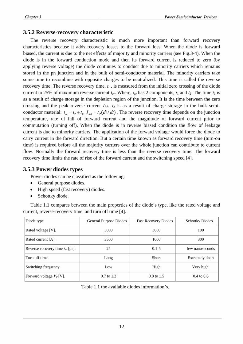
Chapter 3 Power Semiconductor Devices
12
3.5.2 Reverse-recovery characteristic The reverse recovery characteristic is much more important than forward recovery
characteristics because it adds recovery losses to the forward loss. When the diode is forward biased, the current is due to the net effects of majority and minority carriers (see Fig.3-4). When the diode is in the forward conduction mode and then its forward current is reduced to zero (by applying reverse voltage) the diode continues to conduct due to minority carriers which remains stored in the pn junction and in the bulk of semi-conductor material. The minority carriers take some time to recombine with opposite charges to be neutralized. This time is called the reverse recovery time. The reverse recovery time, trr, is measured from the initial zero crossing of the diode current to 25% of maximum reverse current Irr. Where, trr has 2 components, t1 and t2. The time t1 is as a result of charge storage in the depletion region of the junction. It is the time between the zero crossing and the peak reverse current IRR. t2 is as a result of charge storage in the bulk semi-conductor material: 2 1 1, .( / ) rr RRt t t I t di dt= + = . The reverse recovery time depends on the junction temperature, rate of fall of forward current and the magnitude of forward current prior to commutation (turning off). When the diode is in reverse biased condition the flow of leakage current is due to minority carriers. The application of the forward voltage would force the diode to carry current in the forward direction. But a certain time known as forward recovery time (turn-on time) is required before all the majority carriers over the whole junction can contribute to current flow. Normally the forward recovery time is less than the reverse recovery time. The forward recovery time limits the rate of rise of the forward current and the switching speed [4].
3.5.3 Power diodes types Power diodes can be classified as the following: • General purpose diodes. • High speed (fast recovery) diodes. • Schottky diode.
Table 1.1 compares between the main properties of the diode’s type, like the rated voltage and current, reverse-recovery time, and turn off time [4].
Diode type General Purpose Diodes Fast Recovery Diodes Schottky Diodes
Rated voltage [V]. 5000 3000 100
Rated current [A]. 3500 1000 300
Reverse-recovery time trr [µs]. 25 0.1-5 few nanoseconds
Turn off time. Long Short Extremely short
Switching frequency. Low High Very high.
Forward voltage VF [V]. 0.7 to 1.2 0.8 to 1.5 0.4 to 0.6
Table 1.1 the available diodes information’s.

Chapter 3 Power Semiconductor Devices
13
IRR
IF
IRR/4 t
t 1 t 2
trr
(e)
ViVF
-VR
t1
tt10
0
0
0
-VR
V
IIO
Pn-Pnoat Junction
t
t
t
FF
L
VIR
≈
RR
L
VIR
≈
t2
Forwardbias
MinorityCarrier
storage, ts
Transitioninterval, tt
(a)
(b)
(c)
(d)
Fig.3-4 Diode characteristics.
(a).Input waveform applied to the diode in Fig.3-3(a), (b) The excess-carrier density at the junction, (c) The diode current, (d) The diode voltage, (e) Diode reverse-recovery
characteristics.
3.6 Insulated Gate Bipolar Transistor (IGBT) A modern power transistor is the Insulated Gate Bipolar Transistor (IGBT), It operates as a
transistor with high-voltage and high-current capability and moderate forward voltage drop during the conduction state. The IGBT has progressed to become a choice in a wide range of low and medium power applications going up to several megawatts and even tens megawatts. Thus IGBT is of some importance to FACTS controllers [3], [4].
The IGBT is a voltage controlled device. It has high impedance like a MOSFET and low on-state conduction like BJT. Fig.3-5 shows the basic silicon cross-section of an IGBT. Its construction is same as power MOSFET except that the n+ layer at the drain in a power MOSFET is replaced by P+ substrate called collector. The IGBT has three terminals gate (G), collector (C), and emitter (E). With the collector and the gate voltage positive with respect to the emitter the device is in forward blocking mode. When the gate to emitter voltage becomes greater than the threshold voltage of IGBT, an n- channel is formed in the P-region. Now the device is in forward conduction state. In this state p+ substrate injects holes into the epitaxial n- layer. Increasing in the collator to emitter

Chapter 3 Power Semiconductor Devices
14
voltage will result in increasing of injected holes concentration and finally a forward current established.
GateGate
Emitter
Collector
p+
pn- epi
n+
n+n+
E
G
C
i1i2
C
G
E
(a) (b) (c)
Fig.3-5 IGBT transistor: (a) IGBT transistor structure and the location of the equivalent circuit, (b) the equivalent circuit, (c) IGBT symbol.
The advantage of the IGBT is its fast turn-on and turn-off because it is more like a majority carrier (electrons) devices. It can be therefore used in pulse width modulator (PWM) converters operating at high frequency. On the other hand being a transistor device, it has higher forward drop voltage compared to thyristor type devices such as GTOs. Nevertheless, the IGBT has become a workhorse for industrial applications and has reached sizes capable of application in the range of 10MW or more. The transistor devices, such as MOSFETs and IGBTs, potentially have current-limiting capabilities by controlling the gate voltage. During this current-limiting action, the device losses are very high, and in high-power applications, current-limiting action can only be used for very short periods of a microsecond. Yet, this time can be enough to allow other protective actions to be taken for safe turn-off of the devices. This feature is extremely valuable in voltage-sourced converters, in which fault current can rapidly rise to high levels due to the presence of a large DC capacitor across the converter. On the other hand, with fast sensing, combined with the fast turn-off of the advanced GTOs, an effective turn-off can be achieved within 2-3µs. This method will also spare the devices from high-power dissipation and sacrifice their useable capacity. The turn-off time of the conventional GTOs is too long for high-speed protective turn-off. IGBT is coming from a low-power end, has been pushing out conventional GTO’s rating go up (as available packaged parallel-IGBTs). This is because the conventional GTO’s have serious disadvantages which are basically related to the large gate-drive requirements, the slow-switching and the high-switching losses. The IGBT has its own generic limitations, including: high forward voltage drop, complexities with providing double-side cooling, the nature of the repetitive MOS on the chip limits that can be achieved in increased blocking voltage. Also, IGBT production needs much clearer production facility. A major advantage for IGBT for high-power applications is its low-switching losses, fast switching, and current-limiting capability. However, with the advanced GTOs, and MCT’s, which will be discussed later, there is a prospect for major advances for devices suitable for a wide range of FACTS Controllers. On the other hand, future outcome often depends on the market forces of volume production, and this is a favor of the IGBTs continuing to push its application to

Chapter 3 Power Semiconductor Devices
15
higher power levels. Fig.3-6 shows the output characteristic of the collector current IC versus collector to emitter voltage VCE for given value of gate to emitter voltage VGE [3], [4].
IC
VCEVCE(sat)
VGE
Fig.3-6 IGBT current-voltage (IC-VGE) characteristics for a given value of VCE.
3.6.1 Switching characteristic of the IGBT The switching process may be seen as a combination of switching performance of a MOSFET
and BJT which did not discussed here. Fig.3-7 shows the switching characteristic of an IGBT. The turn-on time consists of a delay time td(on) and a rise time tr. The turn on delay time is the time required by the leakage current ICE to rise to 0.1IC, where IC is the final value of the collector current.
The rise time is the time required for the collector current to rise from 0.1IC to its final value IC. After turn-on, the collector-emitter voltage VCE will be very small during the steady state conduction of the device [3]. The turn-off time consists of the delay off time td(off) and fall time tf. The off time delay is the time during which the collector current falls from IC to 0.9IC and VGE falls to threshold voltage VGET. During the fall time tf the collector current falls from 0.90IC to 0.1IC. During the turn-off time the interval collector-emitter voltage rises to its final value VCE. IGBT’s are voltage controlled power transistors. They are faster than BJT’s, but still not quite as fast as MOSFET’s. The IGBT’s offer superior drive and output characteristics compared to BJT’s. IGBT’s are suitable for high voltage; high currents and frequencies up to 20KHz. IGBTs are available up to 1400V, 600Amps and 1200V, 1000Amps [4].
3.7 Types of high-power thyristor devices Technically, the terms “thyristor” and “Silicon Controlled Rectifier (SCR)” are applied to a
basic family of four-layer controlled semiconductors devices in which turn-on and turn-off depends on pnpn regenerative feedback. The name Silicon Controlled Rectifier (SCR) was given by inventors and commercially pioneered by GE (General Electric). In the text of a device which has a turn-on but no turn-off capability, the term SCR was later changed by others to thyristors. With the emergence of a device with both turn-on and turn-off capability, named Gate Turn-off Thyristors referred to as GTO, the device with just the turn-on capability began to be referred to as “conventional thyristor” or just “thyristor”. Other members of the thyristor or SCR family have acquired other names based on acronyms. In use of the term thyristor is generally meant to be the conventional thyristor.

Chapter 3 Power Semiconductor Devices
16
IC
VCE
VGET
0.1 ICE
0.9 ICE
td(on)
t
trtd(off) tf
VGE
t
t
0.9 VCE
0.1 VCE
td(off) tf
( ) ( )
( )
on d on r
off d off f
t t t
t t t
= +
= +
Fig.3-7 Switching characteristic of an IGBT.
The thyristor starts to conduct in forward direction when a trigger current pulse is passed from gate to cathode, and rapidly latches into full conduction with a low forward voltage drop (1.5V to 3V depending on the type of the thyristor and the current). As mentioned previously, the conventional thyristor cannot force its current back to zero. Instead, it relies on the current itself for the current comes to zero. When the circuit current comes to zero, the thyristor recovers in a few microseconds of reverse backing voltage, following which it can block the forward voltage until the next turn-on pulse is applied. Because of their low cost, high frequency, ruggedness, and high voltage and high current capability, conventional thyristors are extensively used when circuit configuration and cost-effective application do not call for turn-off capability. Often the turn-off capability does not offer sufficient benefits to justify higher cost and losses of the devices. The conventional thyristor has been the device of choice for most HVDC projects, some FACTS controllers, and a large percentage of industrial applications. It is often referred to as the workhorse of the power electronics business. The several versions of thyristors with turn-on capability among these and relevant to the FACTS technology are presented in the following sections [3].
3.7.1 Thyristors The thyristor are a family of four-layer devices. A thyristor latches into full conduction in its
forward direction when one of its electrodes (anode) is positive with the respect to its other

Chapter 3 Power Semiconductor Devices
17
electrodes (cathode) and turn-on voltage or current signal (pulse) is applied to the third electrode (gate) (see Fig.3-8(a)). Latched conduction is a key to low on-state conduction losses, called base. Most thyristors are designed without gate-controlled turn-off capability, in which case the thyristor recovers from its latched conducting state to a non-conducting state only when the current brought to zero by other means. Other thyristors are designed to have both gate-controlled turn-on and turn-off capability.
The thyristor may be designed to block in both the forward and reverse direction (referred as a symmetrical device) or it may be designed to block only in the forward direction (referred to as asymmetrical device). Thyristors are the most important devices for FACTS Controllers. Compared to thyristors, transistors generally have superior switching performance, in terms of faster switching and lower switching losses. On the other hand, thyristors have lower on-state conduction losses and higher power handling capability than transistors. Advances are continuously being made to achieve the best of both, i.e., low on-state losses, while increasing their power handling capability.The Thyristor (SCR Silicon Controlled Rrectifier), which is shown in Fig.3-8, is a three-junction, four-layer device. The thyristor is a unidirectional switch, which once turned on by a trigger pulse, latches into conduction with the lowest forward voltage drop of 1.5V to 3V at its continuous rated current. It does not have the capability to turn off the current, so that it recovers its turned-off state only when the external circuit causes the current to come to zero. The thyristor is referred to as the workhorse of power electronics. In a many applications, turn-off capabilityy is not necessary. Without turn-off capability, the resulting device can have higher voltage and/or rating, cost less than one-half, require a simple device control circuit, has lower losses, etc, compared to device with turn-off capability. Therefore, the choice in favor of a more expensive and higher loss device with turn-off capability will occur when there is a decisive application advantage [3], [4].
As shown in Fig.3-8(c), the thyristor is equivalent to the integration of two transistors, pnp and npn. When a positive gate trigger is applied to the p gate of the upper npn transistor with respect to the n+ emitter (cathode), it starts conducting. The current through the npn transistor becomes the gate current of the pnp transistor as shown by the arrows, causing it conducts as well. The current through this pnp transistor in turn becomes the gate current of the npn transistor giving a regenerative effect to latched conduction with low forward voltage drop with the current flow essentially limiting the external circuit. What is important is that due to the internal regenerative action into saturation, once the thyristor is turned on, the internal n+ and n layers become saturated with electrons and holes and act like a short circuit in the forward direction.
The whole device behaves like a single pn junction device (a diode). Thus, its forward on-state voltage drop corresponds to only one junction (even though it has three junction) compared to two junction in transistor devices such as MOSFET and IGBT. The turn-off time, which can be a few tens of microseconds, depends on the reverse voltage after zero current and has to be carefully considered for specific applications. This turn-off time must elapse before any positive voltage can safely be applied [3], [4].
In large thyristor wafers, the gate structure is brought out through the cathode side at the top. Several amplifying stages are provided in concentric circles at the centre in order to decrease the required external gate pulse current. It is essential to rapidly spread out turn-on current over the

Chapter 3 Power Semiconductor Devices
18
whole device. It is also appropriate to consider adding another high-voltage, very low current external pilot thyristor in order to increase the gain and reduce the gate turn-on power at the thyristor level. Such a device would be expensive because of the very low current rating. A thyristor can also be turned off by hitting the gate region with light of appropriate bandwidth. The direct light trigger thyristor allows the triggering of the thyristor directly from the control circuit via optical fiber. As an alternative, the external pilot thyristor, which is mentioned above, may be a light triggered thyristor with the main thyristor as an electrically triggered thyristor.
Gate
Cathode
Anode
P
Anode
CathodeGate
Pn
n+
Gate
P
Anode
Cathode
P
n
n+
n
P
Cathode
Anode
Gate
P
P
P
n
n
n
Turn-on
(a) (b) (c) (d) Fig.3-8 Thyristor (a) Thyristor symbol, (b) Thyristor structure, (d) two-transistor structure,
and (d) Thyristor equivalent circuit.
The application of a positive anode to the cathode voltage with high rate of rise (dv/dt) can also turn on the device. This happens because the capacitive coupling of the cathode to gate and the high dv/dt causes just enough current to turn the device on. This is not a safe way to turn on a thyristor. Turning-on a thyristor in such away can occur at weak spot, which does not spread rapidly and may damage the device. Unsafe turn-on will also occur if the forward voltage is too high, which creates charge carriers in weak spot through acceleration of internal charge carriers. This also suggests that the device can be made with deliberately designed weak spot from where safe turn-on can be designed into the device. Such devices with self-protection and optional triggering have been introduced in recent HVDC projects [3], [4], and [5].
Another important aspect is that when a turn-on pulse is applied, there has to be enough anode-to-cathode forward voltage, or rate of rise of voltage, to cause a rapid turn-on. Insufficient voltage can lead to soft turn-on with device voltage falling slowly while the current is rising. This can lead to a high turn-on loss in certain areas of the device and cause a possible damage. Depending on the application, the device has to be designed for the specific minimum turn-on voltage and the turn-on pulse is blocked if the forward voltage is inadequate. At high temperature, the thyristor has a negative temperature coefficient. Thus, it has to be designed to ensure a uniform internal turn-on and turn-off. Being a high voltage device, it includes doping-based carriers as well as a large number of intrinsic carriers. With higher temperature, the number of thermal carriers and hence total carriers increases and this leads to a lower forward voltage drop. Once a thyristor is turned on there is a need to sustain a minimum anode-cathode current for the device to stay turned on. This

Chapter 3 Power Semiconductor Devices
19
minimum current is usually a percentage of the device current. The gate-drive is usually arranged to send another turn-on pulse as needed. Generally thyristors have a large overload capability. They have two times normal over-current capability for several seconds, ten times for several cycles, and 50 times fully short-circuit for one cycle [5], [6].
3.7.1.1 Switching characteristic of thyristor (SCR) The Switching operation of an SCR is shown in Fig.3-9. Some of its important features are:
• Initially when forward voltage is applied across the device, the off state or static dv/dt has to be limited so that the device does not turn on.
• When gate current IG is applied (with anode in forward blocking state), there is a finite delay time before the anode current starts building up. This delay time, td, is usually a fraction of microseconds.
• After the delay time, the device conducts and the anode current builds up to the full value IT. The rate of rise of the anode current during this time depends upon the external load current. If during turn-on, the anode current builds up too fast which may be damage the device. The initial turn-on of the device occurs near the gate cathode periphery and then the turn-on area of device spreads across the entire junction with a finite velocity. If IT rises at a rate faster than the spreading velocity, then the entire current IT is confined to a small area of the device eventually overheats the junction and may destroy the device. Therefore, it is necessary to limit the turn-on di/dt of the circuit to less than the safe di/dt that can be tolerated by the device.
IT
IG
t
t
t
VAK
td
VAK
tr
VRRMVR
tqVDRM
Turn ondi/dt
Commutating di/dt
Off state dv/dt
IRM
Reapplied dv/dt
Fig.3-9 Switching characteristics of the thyristor.
• During conduction, the middle junction is heavily saturated with minority carries and the gate
has no further control on the device. The device drop voltage under this condition is typically about 1V.
Chapter 3 Power Semiconductor Devices
20
• From the conducting state, the SCR can be turned off by temporarily applying a negative voltage across the device from external circuit. When reverse voltage is applied, the forward current first goes to zero and then the current builds up in the reverse direction with the commutation di/dt. The commutation di/dt depends on the external commutating circuit. The reverse current flow across the device to sweep the minority carries across the junction. At maximum reverse recovery current IRM, the junction begins to block causing decay of reverse current. The fast decay of the recovery current causes a voltage overshoot VRRM across the device due to the leakage inductance effect. At zero current, the middle junction is still forward biased and the minority carries in the vicinity must be given time for recombination. The reapplied dv/dt has to be limited so that no spurious turn-on occurs. The device turn-off time, tq, is a function of Tj (the temperature of the junction), IT, VR, VDRM, di/dt, dv/dt and VG.
Thyristors are available for power electronics system application with voltage ratings up to 6000V and current ratings about 6000Amps [4].
3.7.2 Gate turn-off thyristor (GTO) Invented at GE, is now referred to as a GTO thyristor or simply a GTO. Like a conventional
thyristor, it turns on in a fully conducting mode (latched mode) with a low forward voltage drop when a turn-on current pulse is applied to its gate with respect to its cathode. Like a conventional thyristor, the GTO will turn off when the current naturally comes to zero, but the GTO also has Turn-off capability when a turn-off pulse is applied to the gate in reverse direction. With an adequate turn-off pulse, The GTO rapidly turns off and recovers to withstand the forward voltage and be ready for the next turn-on pulse. The GTO is a widely used device for FACTS Controllers. However, because of its bulky gate drivers, and slow turn-off and costly snubbers, it is likely to be replaced in the coming years by more advanced GTOs Thyristors. These Advanced GTOs, which in turn are part of the thyristor family, are explained later on. Basically, the gate turn-off (GTO) thyristor is similar to the conventional thyristor and essentially most of the aspects discussed in the last section apply to GTOs as well. The GTO, which is shown in Fig.3-10, like the thyristor is a latched-on device, but it is also a latched-off device. Discussion of the GTO in this section refers to conventional GTO without the recent advances made in devices made under different acronyms which are discussed in later sections. Considering the equivalent circuit shown in Fig.3-10(d) which is the same as the circuit shown in Fig.3-8(c) of the thyristor except that the turn-off has been added between the gate and the cathode in parallel with the gate turn-on (shown only by arrows in the equivalent circuit). If large pulse current is passed from the cathode to the gate to take away sufficient charge carriers from the cathode, i.e., from the emitter of the upper pnp transistor, the npn transistor will be drawn out of the regenerative action.
As the upper transistor turns off, the lower transistor is left with an open gate, and the device returns to non-conducting state. However, the required gate current for turn-off is quite large. Whereas the gate current pulse required for turn-on may be 3-5 %, i.e., 30 A for only 10 µsec for a 1000Amps devices, the gate current required for turn-off would be more like 30-50%, i.e., 300 A or larger for 20-50µsec [3], [4]. The voltage required to drive the high current pulse is low (about 10-20V) and being a pulse of 20-50µsec duration and the energy required for turn-off is very large. Yet the losses are large enough to be a significant economic liability in terms of losses and cooling requirements, when considering the number of valve turn-off events in a converter. Turn-off energy

Chapter 3 Power Semiconductor Devices
21
required is 10 to 20 times that is required for GTO turn-on, and the GTO turn-on required energy is 10 to 20 times that required for a thyristor.
Gate
Cathode
Anode
P
Anode
CathodeGate
n
n+
Pn+
Turn-on
Turn-off
Cathode
Anode
Gate
P
P
P
n
n
n
(a) (b) (c)
Fig.3-10 Gate turn-off thyristor (a) GTO -symbol, (b) -structure and (c) -equivalent circuit.
The cost and size of the turn-off circuits for GTO are comparable to the device costs itself. Another consideration is that the turn-off has to be uniformly effective over the entire device. Whereas in a thyristor, there is one cathode with a single gate structure spread out across the device, a successful GTO turn-off requires dividing up the cathode into several thousand islands with a common gate-line which surrounds each and every cathode islands in Fig.3-11. Thus, a GTO consists of a large number of thyristor cathodes with a common gate, a drift region, and an anode. Given the complex structure, state-of-the-art GTOs do not have built-in amplifying gates. Consequently, the total available area on the device for the cathode decreases to about 50% compared to a thyristor. Therefore, GTOs forward voltage drop is about 50% higher than that of a thyristor but still 50% lower than that of a (IGBT) of the same rating [5].
(a) (b)
Fig.3-11 (a) A picture of GTO surface (b) A picture of GTO wafer including definition of radii rv.
The general process of making GTOs is about the same as that for thyristors, although due to complications of the cathode and the grid distribution, its process requires a cleaner room, yield

Chapter 3 Power Semiconductor Devices
22
may be less, and cost perhaps twice that of thyristor for the same converter ratings. As for a thyristor, there are trade-offs between voltage, current, di/dt, dv/dt, switching times, forward losses, switching losses, etc., for the GTO design. Large sector of the market of GTOs is for voltage-sourced converters in which a fast recovery diode is connected in reverse across each GTO which means that GTOs do not need reverse voltage capability. This also provides beneficial tread-offs for other parameters, particularly the voltage drop and higher voltage and current ratings. This is achieved by the so-called buffer layer, a heavily doped n+ layer at the end of the n- layer. Such GTOs are known as asymmetric GTOs. Like a thyristor, the continuous operating junction temperature limit is about 100oC, after making allowance for the fault current requirements. Like a thyristor, a GTO is capable of surviving a high, short-time over current (10 times for one offset cycle) as long as it is not required to turn off that current. Failure mechanisms are also similar and the edge requires appropriate contouring to reduce voltage stress and passivation to avoid a flashover around the edge [7], [8]. In a thyristor, the current zero is brought about by the external system. The voltage across the device automatically becomes negative immediately after the current zero. On the other hand, the GTO is turned off while the circuit is driving in the forward direction. Therefore, for successful turn-off it is necessary to reduce the rate-of-rise of forward voltage with the help of a damping circuit. In a GTO, the anode side pn- junction is lightly doped and designed to support almost all of the blocking voltage, essentially on the n-side. On the other hand, the cathode side pn junction is heavily doped on both sides and the breakdown voltage may be about 20V [5], [6].
3.7.2.1 Switching characteristics of GTO (turn-on and turn-off process) Apart from the gate driver power, GTOs also have high switching losses and it is important to
appreciate the turn-on and turn-off process with associated device stresses and losses. Fig.3-12 shows simplified waveforms for the turn-on and the turn-off processes. For turn-on, a 10µs current pulse of greater than 5% of the load current with a fast rise time limited largely by the gate circuit inductance is applied from the gate to cathode. However, there is a delay of microseconds, before the anode-cathode current begins to rise and the voltage begins to fall.
The current rises at the rate limited by the circuit as required for safe turn-on of the device such that all cathode islands turn on evenly. Also, given the circuit topology of the Voltage-Sourced Converter, the GTO turn-on is accompanied by turning off the reverse-conducting diode in another valve of the same phase. Therefore the GTO has to turn-on the main circuit current pulse a large reverse leakage current of the diode. During this process of rising current, the anode-cathode voltage falls slowly in accordance to the plasma spreading time, ultimately to its on-state low-voltage level. Following the full turn-on, it is necessary to maintain some gate current of about 0.5% to ensure that the gate does not unlatch; this current is known as back -porch. GTO turn-on losses result from simultaneous existence of voltage and current, made more difficult by current overshoot corresponding to the reverse current of a diode, mentioned above.
The turn-off process in the GTO is initiated by a negative gate current. Due to the high conductivity of the p-base, holes arriving from the anode partially flow to the negatively polarized gate contact. During the storage time, the current progressively filaments towards the middle of the cathode segments, until the filaments are finally “pinched off”. At this instant, the anode current falls rapidly, and both the pn+ and pn junctions are again able to sustain voltage.

Chapter 3 Power Semiconductor Devices
23
Turn ongate pulse
Turn on
v i
Turn off gate pulse
Turn off
vi
(a) (b) Fig.3-12 GTO turn-on and turn-off process: (a) turn-on and (b) turn-off.
The filamentation of the current, towards the cathode centers, reduces the active silicon area during the critical turn-off phase. This would be a minor limitation where it is not compounded by the filamentating current tending to commutate to those cathode areas remotely located from the extinguishing gate current. This re-distribution of the cathode current continues during the storage time (tens of microseconds) and culminates with a rising anode voltage and a falling cathode current. It is this phase which requires the presence of a snubber (i.e. a capacitance) across the device to limit the reapplied dv/dt to between 500 and 1000 V/ms. Fig.3-13 illustrates this short phase in which both anode voltage and cathode current coexist with the danger of re-triggering that this represents [4], [5], [6], and [8]. The GTOs principle handicap compared to IGBT discussed before has been its large gate turn-off drive requirements. This in turn results in long turn-off time, lower di/dt and dv/dt capability, and therefore costly turn-on and turn-off snubber circuits adding to the cost and losses. Because of its slow turn-off, the GTO can be operated in PWM converters at a relatively low frequency (up to a few hundred Hz), which is, however, sufficient for high-power converters. On the other hand, it has lower forward voltage drop and is available in larger rating than IGBT. GTO has been utilized in FACTS controller of several hundreds of MWs [5], [6], and [7].
3.7.3 MOS Turn-Off Thyristor The Silicon Power Corporation (SPCO) has developed the MTO Thyristor, which is a
combination of a GTO and MOSFETs. Together they overcome the limitation of GTO regarding its gate-driver power, snubber circuit, and dv/dt limitation. Unlike the IGBT (discussed before), the MTO structure is not implanted on the entire of the device surface, but instead the MOSFETs are located on the silicon all around the GTO to eliminate the need for high-current GTO turn-off pulse. The GTO structure is essentially retained for advantages of high voltage (up to 10kV), high current (up to 4kA), and lower forward conduction losses than IGBTs.

Chapter 3 Power Semiconductor Devices
24
Conducting thyristor GTO zone Blocking transistor
Fig.3-13 Conduction and conventional Turn-off of a GTO.
With the help of these MOSFETs and tight packaging which minimize the stray inductance in the gate-cathode loop, the MTO becomes significantly more efficient than the conventional GTO, requiring drastically smaller gate drivers while reducing the charge storage time on turn-off, providing improved performance and reduction of system costs. As before, the GTO is still provided with double-sided cooling and lends itself to thin packaging technology for even more efficient removal of heat from the GTO. Fig.3-14 shows the symbol, structure, and equivalent circuit of MOS turn-on thyristor. The turn-off in MTO can be much faster; 1-2µs and the losses corresponding to the storage time are almost eliminated, this also means high dv/dt, and much smaller snubber capacitors and elimination of the snubber resistor [3], [4].
3.7.4 Emitter Turn-on Thyristor (ETO)
Similarly, MTO, ETO is another variation of exploiting the virtues of both the thyristor and the transistor, i.e., GTO and MOSFET. ETO was invented at Virginia Power Electronics Centre in collaboration with SPCO. The EMO symbol and equivalent circuit are shown in Fig.3-15. As shown in Fig.3-15(b), a MOSFET T1 is connected in series with the GTO and a second MOSFET T2 is connected across this series MOSFET and the GTO gate. Actually T1 consists of several N-MOSFETs and T2 consists of several P-MOSFETs packaged around the GTO in order to minimize the inductance between the MOSFETs and the gate cathode of the GTO. N- and p-MOSFETs and GTOs were commercially available devices made in large quantities [3].
The ETO has two gates: one is the GTOs own gate used for turn-on and the other is in series MOSFET gate used for turn-off. When the turn-off voltage signal is applied to the n-MOSFET, it turns off the transfer of all the current away from the cathode (n emitter of the upper transistor of the GTO) into the base via MOSFET T2, thus stopping the regenerative latched state and a fast turn-

Chapter 3 Power Semiconductor Devices
25
off. It is important to note that the MOSFETs see high voltage, no matter how high the ETO voltage. T2 is connected with its gate shorted to its drain and hence voltage across it’s clamped at a value slightly higher than its threshold voltage and the maximum voltage across T1 cannot exceed that across T2 [3], [7], and [8].
Turn-offgate
Cathode
Anode
FETTurn-on
gate
P
Anode
Cathode
Turn-ongate
n
n+
Pn+
Turn-off gate FET Cathode
Anode
Turn-on
Turn-offFET
Cathode
Anode
Turn-on
Turn-off
P
P
P
n
n
n
(a) (b) (c) (d)
Fig.3-14 MOS Turn-off (MTO) thyristor (a) MTO symbol, (b) MTO structure; (c) MTO equivalent circuit, and (d) more detailed equivalent circuit.
Turn-off
Cathode
Anode
Turn-on
P-MOSFET
Cathode
Anode
Turn-on
Turn-off
N-MOSFET
T2
T1
(a) (b) (c)
Fig.3-15 Emitter Turn-off (ETO) thyristor: (a) ETO symbol, (b) ETO equivalent circuit, and (c) ETO structure.
3.7.5 Integrated Gate-Commutated Thyristor (GCT and IGCT) The gate-commutated thyristor (GCT) is a hard-switched GTO involving very fast and large
current pulse, as large as the full rated current, which draws out all the current from the cathode into the gate in 1µsec to ensure a fast turn-off. Its structure and its equivalent circuit are the same as that of a GTO. The IGCT is a device with added value on GCT; including a multilayered printed circuit
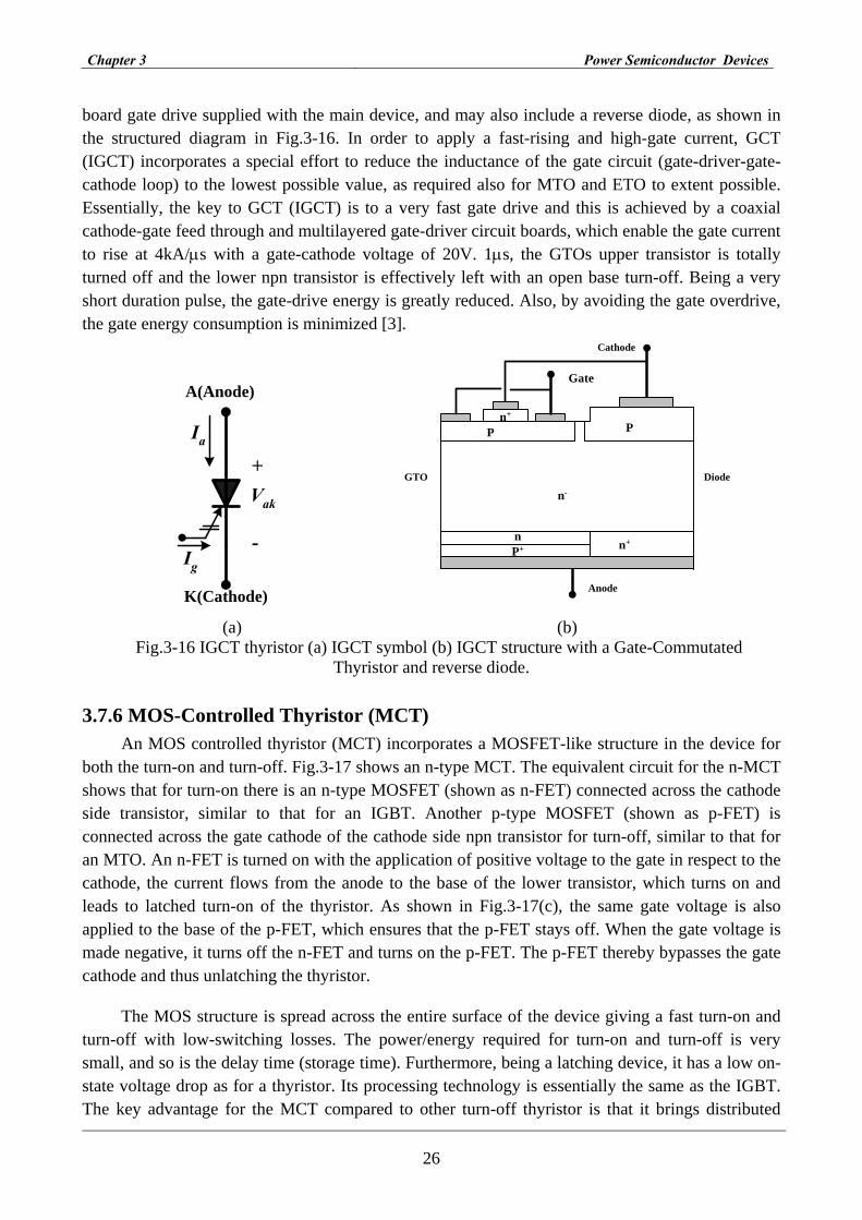
Chapter 3 Power Semiconductor Devices
26
board gate drive supplied with the main device, and may also include a reverse diode, as shown in the structured diagram in Fig.3-16. In order to apply a fast-rising and high-gate current, GCT (IGCT) incorporates a special effort to reduce the inductance of the gate circuit (gate-driver-gate-cathode loop) to the lowest possible value, as required also for MTO and ETO to extent possible. Essentially, the key to GCT (IGCT) is to a very fast gate drive and this is achieved by a coaxial cathode-gate feed through and multilayered gate-driver circuit boards, which enable the gate current to rise at 4kA/µs with a gate-cathode voltage of 20V. 1µs, the GTOs upper transistor is totally turned off and the lower npn transistor is effectively left with an open base turn-off. Being a very short duration pulse, the gate-drive energy is greatly reduced. Also, by avoiding the gate overdrive, the gate energy consumption is minimized [3].
Vak
+
-
Ia
Ig
A(Anode)
K(Cathode)
P+
Anode
Cathode
Gate
n-
n+
Diode
n
P P
GTO
n+
(a) (b)
Fig.3-16 IGCT thyristor (a) IGCT symbol (b) IGCT structure with a Gate-Commutated Thyristor and reverse diode.
3.7.6 MOS-Controlled Thyristor (MCT) An MOS controlled thyristor (MCT) incorporates a MOSFET-like structure in the device for
both the turn-on and turn-off. Fig.3-17 shows an n-type MCT. The equivalent circuit for the n-MCT shows that for turn-on there is an n-type MOSFET (shown as n-FET) connected across the cathode side transistor, similar to that for an IGBT. Another p-type MOSFET (shown as p-FET) is connected across the gate cathode of the cathode side npn transistor for turn-off, similar to that for an MTO. An n-FET is turned on with the application of positive voltage to the gate in respect to the cathode, the current flows from the anode to the base of the lower transistor, which turns on and leads to latched turn-on of the thyristor. As shown in Fig.3-17(c), the same gate voltage is also applied to the base of the p-FET, which ensures that the p-FET stays off. When the gate voltage is made negative, it turns off the n-FET and turns on the p-FET. The p-FET thereby bypasses the gate cathode and thus unlatching the thyristor.
The MOS structure is spread across the entire surface of the device giving a fast turn-on and turn-off with low-switching losses. The power/energy required for turn-on and turn-off is very small, and so is the delay time (storage time). Furthermore, being a latching device, it has a low on-state voltage drop as for a thyristor. Its processing technology is essentially the same as the IGBT. The key advantage for the MCT compared to other turn-off thyristor is that it brings distributed

Chapter 3 Power Semiconductor Devices
27
MOS gates for both turn-on and turn-off, very close to the distributed cathodes, resulting in fast-switching and low switching losses for a thyristor device. Therefore, the MCT represents the near-ultimate turn-off thyristor with low on-state and switching losses, and the fast-switching device needed for high-power advanced converters with active filtering capability [3].
Gate
Cathode
Anode
SiOP+
P+
P
P+
n nn+
Anode
CathodeGate
SiO
n
P
P
Cathode
Anode
P-MOSFET
N-MOSFET
n
Gat
e
(a) (b) (c)
Fig.3-17 MOS-Controlled Thyristor (MCT) (a) MCT symbol, (b) MCT structure (c) MCT equivalent circuit.
3.8 Control characteristic of power devices The power semiconductor switching devices can be operated as switches, e.g., by applying
control signals to the gate terminal of thyristors (or to the base of bi-polar transistors). The required output is obtained by varying the conduction time of the switching devices. Fig.3-18 below shows the output voltages and the control characteristics of commonly used power semiconductor switching devices. Once a thyristor is in a conduction mode, the gate signal of either positive or negative magnitude has no effect. When a power semiconductor switching device is in the normal conduction mode, there is a small drop across the device. In the output voltage waveforms shown, these voltage drops are considered negligible. According to that, the power semiconductor switching devices can be classified based in the following:
• Uncontrolled turn-on and turn-off (e.g. diode). • Controlled turn-on and uncontrolled turn-off (e.g. SCR). • Controlled turn-on and off characteristics (e.g. BJT, MOSFET, GTO, SITH (Static Induction
Thyristor), IGBT, SIT, and MCT). • Continuous gate signal requirements (e.g. BJT, MOSFET, IGBT and SIT (Static Induction
Transistor)). • Pulse gate requirement (e.g. SCR, GTO and MCT). • Bipolar voltage withstanding capability (e.g. SCR and GTO). • Uni-polar voltage withstanding capability (e.g. BIT, MOSFET, GTO, IGBT, and MCT). • Bidirectional current capability (e.g. Triac and RCT).

Chapter 3 Power Semiconductor Devices
28
• Unidirectional current capability (e.g. SCR, GTO, BJT, MOSFET, MCT, IGBT, SITH, SIT, and diode) [4].
(a) Thyristor.
(b) GTO/MTO/ETO/IGCT/MCT/SITH (for MCT, the polarity of vG is reversed as shown).
(c) Transistor.
(D) MOSFET/IGBT switch.
Fig.3-18 Control characteristics of power switching devices.

Chapter 4 F ATCS concept and general system considerations
29
4 FACTS concept and general system considerations
Most of the world electric power supply systems are widely interconnected; involving connections inside utilities own territories which extend to inter-utility interconnections and then to inter-regional and international connections. This is done for economical reasons, to reduce the cost of electricity and improve the reliability of the power system.
4.1 Need of transmission interconnection
Interconnections are needed because they are part from delivery. The purpose of the transmission network is to pool power plants and load centers in order to minimize the necessary total power generation capacity and fuel costs. Transmission interconnections enable taking advantage of diversity of load, availability of source, and fuel price in order to supply electricity to the loads at minimum cost with a required reliability. In general, if the power delivery system was made up of radial lines form individual local generators without being part of a grid system, many more generation resource would be needed to serve the load with the same reliability and the cost of the electricity would be much higher. With that perspective, transmission is often an alternative to new generation resource. The power systems of today are mostly mechanically controlled. There is widespread use of microelectronics, computers and high speed communication for control and protection of present transmission systems. However, when operating signals are sent to power circuits, where the final power control action taken, the switching devices are mechanical and there is little high-speed control. Another problem with mechanical devices is that control cannot be initiated frequently, because these mechanical devices tend to wear out very quickly compared to static devices. As a result from the point of view of both dynamic and steady-state operation, the system is really uncontrollable. Power system planners, operators, and engineers have learned to live with this limitation by using a variety of ingenious techniques to make the system work effectively, at the price of providing greater operating margins and redundancies. These represent an asset that can be effectively utilized with prudent use of FACTS technology (Flexible AC Transmission Systems) selectivity. In the recent years, greater demands have been placed on the transmission network and these demands will continue to increase because of the increasing number of nonutility generators and heightened competition among the utilities themselves. Increased demands on transmission, absence of long-term planning, and the need to provide open access for generating companies and customers, all together have created tendencies toward less security and reduced quality of supply. The FACTS technology is essential to alleviate perhaps some but not all of these difficulties are enabling utilities to get the most service from their transmission facilities and to enhance the grid reliability. It is worth mentioning, however, that for many of the capacity expansion, building new lines or upgrading current and voltage capability of existing lines and corridors will be necessary [3].
4.2 Opportunities of FACTS
The most interesting idea for transmission planners is that FACTS technology opens up the opportunities for controlling power and enhancing the usable capacity of present, as well as new and upgrade lines. The possibility that the current through a line can be controlled at reasonable costs enables a large potential of increasing the capacity of existing lines with larger conductors,

Chapter 4 F ATCS concept and general system considerations
30
and use of one of the FACTS Controllers to enable corresponding power to flow through such lines under normal and contingency conditions. These opportunities arise through the ability of the FACTS Control to control the interrelated parameters that govern the operation of transmission systems including series impedance, shunt impedance, current, voltage, phase angle, and the damping of oscillations at various frequencies below the rated frequency. These constraints cannot be overcome while maintaining the required system reliability, by mechanical means without lowering the useable transmission capacity. By proving added flexibility, FACTS controllers can enable a line to carry power closer to its thermal rating. Mechanical switching needs to be supplemented by rapid-response power electronics. It must be emphasized that FACTS is an enabling technology and not one-one-one substitute for mechanical switches. The FACTS technology is not a single high-power controller, but rather a collection of controllers which can be applied individually or in coordination with others to control one or more of the interrelated system parameters mentioned previously. A well-chosen FATCS Controller can overcome the specific limitations of a designated transmission line or corridor. Because all FACTS Controller represent applications of the same basic technology, their production can eventually take advantage of technologies of scale. Just as the transistor is the basic element for a whole variety of microelectronics chips and circuit, the thyristor or high power transistor is the basic element of a variety of high-power electrical controllers.
FACTS Controller also lent itself to extend usable transmission limits in a step-by-step manner with incremental investment as and when required. A planner could foresee a progressive scenario of mechanical switching means and enabling FACTS Controller such that the transmission lines will involve a combination of mechanical and FACTS Controller to achieve the objective in an appropriate, staged investment scenario. The unique aspect of the FACTS technology is that this umbrella concept revealed the large potential opportunity for the power electronics technology to greatly enhance the value of the power system, and thereby unleashed an array of new and advanced ideas to make it a reality [3], [9].
4.3 Basic types of FACTS controller In general, FACTS Controller can be divided into the categories: • Series Controller. • Shunt Controller. • Combined series-series Controllers. • Combined series-shunt Controllers. Fig.4-1(a) shows the general symbol for a FACTS Controller: a thyristor arrow inside a box.
4.3.1 Series Controller: The series controller could have variable impedance, such as a capacitor, a reactor… etc or a
power electronics based variable source of main frequency, subsynchronous and harmonic frequencies (or a combination) to serve the desired need. In principle, all series controller inject a voltage in series with the line. Even variable impedance multiplied by current flowing through it, represents an injected series voltage in the line. As long as the voltage is in phase quadrature with the line current, the series controller supplies or consumes variable reactive power. Any other phase relationship will involve handling of real power as shown in Fig.4-1(b).

Chapter 4 F ATCS concept and general system considerations
31
4.3.2 Shunt controller As in the case of series controllers, shunt controllers may have variable impedance, variable
source, or a combination of these. In principle, all shunt controllers inject current into the system at the point or connection (see Fig.4-1 (c)). Even variable shunt impedances connected to the line voltage causes a variable current flow and hence represents injection of current into the line. As long as the injected current is in phase quadrature with the line voltage, the shunt controllers only supply or consume variable reactive power. Any other phase relationship will involve handling of real power as well [3].
4.3.3 Combined series-series controller This could be a combination of a separate series controller which is controlled in a coordinated
manner in a multi-line transmission system. It could also be a unified controller as shown in Fig.4-1 (d), in which the series controller provides independent series reactive compensation for each line but also transfers real power among the lines via the power link. The real power transfer capability of the unified series-series controller, referred to as Interline Power Flow Controller (IPFC), makes it possible to balance both the real and active power flow in the lines and thereby maximizes the utilization of the transmission system. The term unified means here that the DC terminals of all controller converters are all connected together for real power transfer.
4.3.4 Combined series-shunt controller Combined series-shunt controller could be a combination of a separate shunt and series
controller as shown in Fig.4-1(e), which are connected in a coordinated manner (see Fig.4-1 (e)), or a Unified Power Flow Controller (UPFC) with series and shunt elements as shown in Fig.4-1 (f). In principle, combined shunt and series controllers inject current into the system with the shunt part of the controller and voltage in series in the line with the series part of the controller. However, when shunt and series controllers are unified, there can be a real power exchange between the series and the shunt controllers via the power link [3], [9].
4.4 Relative importance of different types of controllers
It is important to appreciate that the series-connected controller impacts the driving voltage and hence the current and the power flow directly. Therefore, if the purpose of the application is to control the current/power flow and damp oscillations, the series controller for a given MVA size is several times more powerful than shunt controller. As mentioned previously, the shunt controller acts like a current source, which draws or injects the current into the line. The shunt controller is therefore a good way to control the voltage around the point of connection through injection of reactive current (leading or lagging), alone or a combination of active and reactive current for more effective voltage control and damping of voltage oscillation. This is not to say that the series controller cannot be used to keep the line voltage within the specified voltage range. After all, the voltage fluctuations are largely a consequence of the voltage drop in the series impedance of lines, transformers, and generators. Therefore, adding or subtracting the FACTS controller voltage in series (main frequency, sub-synchronous or harmonic voltage and a combination thereof) can be the most cost-effective way to improve the voltage profile.
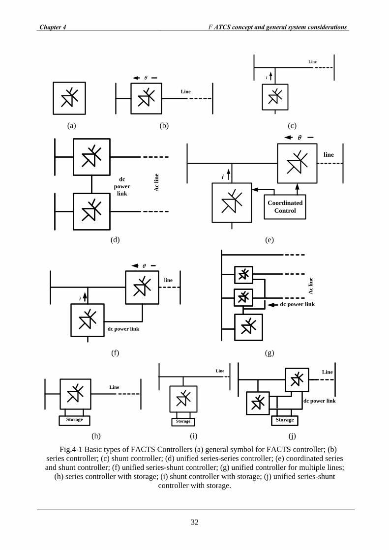
Chapter 4 F ATCS concept and general system considerations
32
θ
Line
i
Line
(a) (b) (c)
Ac
line
dcpower
link
line
CoordinatedControl
i
θ
(d) (e)
line
i
θ
dc power link
dc power linkA
c lin
e
(f) (g)
Line
Storage
Line
Storage
Line
Storage
dc power link
(h) (i) (j)
Fig.4-1 Basic types of FACTS Controllers (a) general symbol for FACTS controller; (b) series controller; (c) shunt controller; (d) unified series-series controller; (e) coordinated series and shunt controller; (f) unified series-shunt controller; (g) unified controller for multiple lines;
(h) series controller with storage; (i) shunt controller with storage; (j) unified series-shunt controller with storage.

Chapter 4 F ATCS concept and general system considerations
33
Nevertheless, the shunt controller is much more effective in maintaining a required voltage profile at a substation bus. One important advantage of the shunt controller is that it serves the bus node independent of the individual lines connected to the bus. The series controller solution may require, but not necessarily, a separate series controller for several lines connected to the substation, particularly if the application reason for contingency outage of any one line. However, this should not be a decisive reason of choosing a shunt-connected controller, because the required MVA size of the series controller is small compared to the shunt controller, and, in any case, the shunt controller doses not provide control over the power flow in the lines. On the other hand, series-connected controllers have to be designed to ride through contingency and dynamic overloads, and ride through or bypass short circuit currents. They can be protected by metal-oxide arrestors or temporarily bypassed by solid-state devices when the fault current is too high, but they have to be rated to handle dynamic and contingency overload.
The above arguments suggest that a combination of the series and shunt controller (see (Fig.4-1(e) and (Fig.4-1(f)) can provide the best of both, i.e., an effective power/current flow and line voltage control. For the combination of series and shunt controllers, the shunt controller can be a single unit serving in coordination with individual line controllers (see Fig.4-1(g)). The arrangement can provide additional benefits (reactive power flow control) with a unified power flow controller. FACTS controllers may be based on thyristor devices with no gate turn-off (only with gate turn-on), or with power devices with gate turn-off capability. In general, the basic controllers with gate turn-off devices are based on DC to AC converters which can exchange active and/or reactive power with the AC system. When the exchange involves reactive power only, they are provided with a minimal storage on the DC side. However, if the generated AC voltage or current is required to deviate form 90 degrees with respect to the line current or voltage, the converter DC storage can augmented beyond the minimum required for the converter operation as a source of reactive power only. This can be done at the converter level to cater to short-term (a few tens of main frequency cycle) storage needs. In addition, another storage source such as a battery, a superconducting magnet, or any other source of energy can be added in parallel through an electrical interface to replenish the converter's DC storage. Any of the converter-based, series, shunt, or combined shunt-series controllers can generally accommodate storage, such as a capacitor, batteries, and superconducting magnets, which bring an added dimension to FACTS technology (see Fig.4-1(h), (i), and (j). The benefits of an added storage system (such as large DC capacitors, batteries, and superconducting magnets) to the controller are significant.
A controller with storage is much more effective for controlling the system dynamics than the corresponding controller without the storage. This has to do with the dynamic pumping of real power in or out of the system as against only influencing the transfer of real power within the system as in the case with controller lacking storage. A converter-based controller can also be designed with so-called high pulse order or with pulse width modulation (PWM) to reduce the low order harmonic generation to a very low level. A converter can in fact be designed to generate the correct waveform in order to act as an active filter. It can also be controlled and operated in a way that it balances the unbalance voltages, involving the transfer of energy between phases. It can do all of these beneficial things simultaneously if the converter is designed [3], [9].

Chapter 4 F ATCS concept and general system considerations
34
4.5 Description and definition of FACTS Controllers
The purpose of this section is to briefly describe and define various, shunt, series, and combine controllers. Before going into a very brief description of a variety of specific FACTS Controllers, it is worth mentioning here that for the converter-based controller, there are two principal types of converters with gate turn-off devices. These are the so-called the Voltage-Source Converters and the Current-Source Converters, As shown in Fig.4-2(a), the Voltage-Source Converter is presented in symbolic form by a box with the gate turn-off device paralleled by a reverse diode, and a DC capacitor as its voltage source. As shown in Fig.4-2(a), the Current-Source Converter is presented by a box with the gate turn-off device with a series diode, and a DC reactor as its current source.
Details of variety of Voltage-Sourced Converters and Current-Sourced Converter suitable for high power applications will be discussed in next two chapters. It would suffice to say that the Voltage-Sourced Converter, unidirectional DC voltage or a DC capacitor is presented to the AC side through a sequential switching of the devices. Through appropriate converter topology, it is possible to vary the AC output voltage in its magnitude and also in any phase relationship to the AC system voltage. The power reversal involves reversal currents, not the voltage. When the storage capacity of the DC capacitor is small, and there is no other power source connected to it, the converter cannot supply or absorb real power for much more than a cycle. The AC output voltage is maintained at 90 degrees with reference to the AC current, leading or lagging, and the converter is used to absorb or supply reactive power only. For the Current-Sourced Converter, the DC current is presented to the AC side through the sequential switching of devices, as AC current, variable in amplitude and also in any phase relationship to the AC system voltage. The power reversal involves reversal of the voltage and not the current. The Current-Sourced Converter is represented symbolically by a box with a power device, and a DC indicator as its current source.
From the overall cost point of view, the voltage-sourced converters seem to be preferred, and will be the basis for the presentations of most converter-based FACTS Controller. One of the facts of life is that those involved with FACTS will have to get used to large number of new acronyms designated by manufactures for their specific products, and by other various papers on new controllers or variations of known controllers, some of these acronyms are: Flexibility of electrical power transmission: The ability to accommodate changes in the electric transmission system or operating conditions while maintaining sufficient steady-state and transient margins [3]. Flexibility AC transmission systems (FACTS): Alternating current transmission systems incorporating power electronic-based and other static controllers to enhance controllability and increase power transfer capability. FACTS controllers: A power electronic-based system and other static equipment that provide control of one or more AC transmission system parameters [3].

Chapter 4 F ATCS concept and general system considerations
35
Line
+ -
Line
Line
+ -
Interface
Stroage
(a) (b)
Line
TCRTSR
TSC Filter
Line
(c) (d) Fig.4- 2 Shunt-connected Controllers (a) Static Synchronous Series Compensator
(STATCOM) based on voltage-sourced and current-sourced converter; (b) STATCOM with storage, i.e., Battery Energy Storage System (BESS), Superconducting Magnet Energy System
and large capacitor; (c) Static VAR Compensator (SVC); (d) Static VAR Generator (SVG), Static VAR System, Thyristor-Controlled Reactor (TCR), Thyristor-Switched Capacitor
(TSC), and Thyristor-Switched Reactor (TSC); (d) Thyristor-Controlled Braking Resistor.
4.6 Shunt connected controllers 4.6.1 Static Synchronous Compensator
A static synchronous generator operated as a shunt–connected static var compensator whose capacitive or inductive output current can be controlled independently by the AC system voltage. The Static Synchronous Compensator (STATCOM) is one of the key FACTS controllers. It can be based on Voltage-Sourced or Current-Sourced Converters. Fig.4-2(a) shows a simple one-line diagram of the STATCOM based on Voltage-Sourced or Current-Sourced Converter. As mentioned

Chapter 4 F ATCS concept and general system considerations
36
before, from an overall cost point of view, the Voltage Sourced Converters seem to be preferred, and will be the basis for presentation of most converter-based FACTS controllers [3].
4.6.2 Static Synchronous Generator (SSG)
A static synchronous generator is a static self-commutated switching power converter is supplied from an appropriate electric energy source and operated to produce a set of adjustable multiphase output voltage, which may be coupled to an AC power system for the purpose of exchanging independently controllable real and reactive power. SSG can be seen a combination of a STATCOM and any energy source to supply or absorb power (see Fig-4-2(b)). The term, SSG generalizes connecting any source of energy including a battery, flywheel, superconducting magnet, large DC storage capacitor, another rectifier/inverter…etc. An electronic interface known as a chopper is generally needed between the energy source and the converter.[3].
4.6.3 Battery Energy Storage System (BESS)
A battery energy storage system is chemical based energy storage system using a shunt-controller, Voltage-Sourced Converters are capable of rapidly adjusting the amount of energy which is supplied to or absorbed form an AC system. Fig.4-2(b) shows a simple one-line diagram in which storage means is connected to a STATCOM. For transmission applications, BESS storage unit size would tend to be a small (a few tens of MWHs). If the short-time converter rating was large enough, it could deliver MWs with a high MW/MWH ratio for transient stability. The converter can also simultaneously absorb or delver reactive power within the converter MVA capacity. [3]:
4.6.4 Superconducting Magnetic Energy Storage (SMES)
A superconducting electromagnetic energy storage device is containing electrical converters that rapidly injects and/or absorbs real and/or reactive power or dynamically controls power flow in AC system. Since the DC current in the magnet does not change rapidly, the power input or output of the magnet is changed by controlling the voltage across the magnet with a suitable electronics interface for connection to a STATCOM.
4.6.5 Static Var Compensator (SVC)
A shunt-connected static Var generator or absorber whose output is adjusted to exchange capacitive or inductive current, this will maintain or control specific parameters of the electrical power system (typically the bus voltage). This is the general term for a thyristor-controlled or thyristor-switched reactor, and/or thyristor-switched capacitor or combination (see Fig.4-2(c)).The SVC is based on thyristors without the gate turn-off capability. It includes separate equipment for leading and lagging vars; the thyristor-controlled or thyristor-switched reactor for absorbing reactive power and the thyristor-switched capacitor for supplying the reactive power. The SVC is considered by some applications as a lower cost alternative to the STATCOM, although this may not be the case if comparison is made based on the required performance and not just the MVA size [3], [9].

Chapter 4 F ATCS concept and general system considerations
37
4.6.6 Thyristor Controlled Reactor (TCR)
A thyristor controller reactor is a shunt-connected, thyristor-controlled inductor whose effective reactance is varied in a continuous manner by partial-conduction control of the thyristor valve. A TCR is a subset of SVC in which the conduction time and hence, the current in a shunt reactor is controlled by a thyristor-based AC switch with firing angle control (see Fig.4-2(c)) [3]
4.6.7 Thyristor-Switched Reactor (TSR)
A thyristor- switched reactor is a shunt-connected, thyristor-switched inductor whose effective reactance is varied in a stepwise manner by full- or zero-conduction operation of the thyristor valve. A TSR (Fig.4-2(c)) is another a subset of the SVC, the TSR is made up of several shunt-connected inductors which are switched in and out by thyristor switches without any firing angle control in order to achieve the required step changes in the reactive power consumed from the system. [3].
4.6.8 Thyristor Switched Capacitor (TSC)
A thyristor switched capacitor is a shunt-connected thyristor-switched capacitor whose effective reactance is varied in a stepwise manner by a full- or zero-conductions of the thyristor valve. A TSC (see Fig.4-2(c)) is also a subset of the SVC in which thyristor based AC switches are used to switch in and out (without firing angle control) shunt capacitors units, in order to achieve the required step change in the reactive power supplied to the system [3].
4.6.9 Static Var Generator or Absorber (SVG)
A static var generator or absorber is a static electrical device, equipment, or system that is capable of drawing controlled capacitive and/or inductive current from an electrical power system and thereby generating or absorbing reactive power. Generally, it would be considered to be consisted of shunt-connected, thyristor-controlled reactor(s) and/or thyristor-switched capacitors. The SVG, as broadly defined by IEEE, is simply a reactive power (var) source that, with appropriate controls, can be converted into any specific or multipurpose reactive shunt compensator [3].
4.6.10 Static Var System (SVS)
A static var system is a combination of different static and mechanically-switched var compensators whose output is coordinated.
4.6.11 Thyristor controlled braking Resistor (TCBR)
A thyristor controlled braking resistor is a shunt-connected thyristor-switched resistor is controlled to aid stabilization of a power system or to minimize the power acceleration of a generating unit during a disturbance. A TCBR involves cycle-by-cycle switching of a resistor (usually a liner resistor) with a thyristor-based AC switch with firing angle control (see Fig.4-2(d)). For lower cost, a TCBR may be thyristor switched, i.e., without firing angle control. However, with firing control, half-cycle firing by half-cycle firing control can be utilized to selectively damp low-frequency oscillations [3].
Chapter 4 F ATCS concept and general system considerations
38
4.7 Series connected controllers 4.7.1 Static Synchronous Series Compensator (SSSC)
A static synchronous series compensator is a static synchronous generator operated without an external electric energy source as a series compensator whose output voltage is in quadrature with and controllable independent of the line current for the purpose of increasing or decreasing the overall reactive voltage drop across the line and thereby controlling the transmitted electric power. The SSSC may include a transiently rated energy storage or an absorbing devices to enhance the dynamic behavior of the power system by an additional temporal real power compensation to increase or decrease momentarily the overall real (resistive) voltage drop across the line.
A SSSC is one of the most important FACTS controllers. It is similar to STATCOM except that the output AC voltage is in series with the line. It can be based on a Voltage-Sourced Converter (see Fig.4-3(a)), or a Current-Sourced Converter. Usually the injected voltage in series would be quite small compared to the line voltage, and the insulation to the ground would be quite high. With an appropriate insulation between the primary and the secondary side of the transformer, the converter equipment is located at the ground potential unless the entire converter equipment is located on a platform duly insulated to the ground. The transformer ratio is tailored to the most economical converter design. (See Fig.4-3(b)) [3], [9].
4.7.2 Interline Power Flow Controller (IPFC)
A interline power flow controller is a recently introduced Controller and thus has no IEEE definition yet. A possible definition is: The combination of two or more Static Synchronous Series Compensators which are coupled via a common DC link to facilitate bi-directional flow of real power between the AC terminals of the SSSC’s, and are controlled to provide independently reactive compensation for adjustment of real power flow in each line and maintain the desired distribution of reactive power flow among the lines. [3], [9].
4.7.3 Thyristor Controlled Series Capacitor (TCSC)
A thyristor controller series capacitor is a capacitive reactance compensator which consists of a series capacitor bank shunted by a thyristor-controlled reactor in order to provide a smoothly variable series capacitive reactance. The TCSC which is seen in Fig.4-3(c) is based on a thyristor without the gate turn-off capability. It is an alternative to the SSSC above and link an SSSC. It is a very important FACTS controller. A variable reactor such as a Thyristor-Controlled Reactor (TCR) is connected across a series capacitor. When the TCR firing angle is 180 degrees, the reactor becomes non-conducting and the series capacitor has its normal impedance. As the firing angle is advanced from 180 degrees to less than 180 degrees the capacitive impedance increases. At the other end, when the TCR angle is 90 degrees, the reactor becomes fully conducting and the total impedance becomes inductive, because the reactor impedance is designed to be much lower than the series capacitor impedance. [3].
4.7.4 Thyristor-switched Series Capacitor (TSSC)
A thyristor-switched series capacitor is a capacitive reactance compensator which consists of a series capacitor bank. It would be shunted by a thyristor-switched reactor to provide a stepwise

Chapter 4 F ATCS concept and general system considerations
39
control of the series capacitive reactance. Instead of the continuous control of the capacitive impedance, the approach of switching inductors at firing angle 90 degrees or 180 degrees but without firing angle control could reduce cost and losses of the Controller (see Fig.4-3(c)). It is reasonable to arrange one of the modules to have thyristor control, while others can be thyristor switched [3].
Line
+ -
Line
+ -
Interface
Stroage
(a) (b)
Line Line
(c) (d)
Fig.4-3 (a) Static Synchronous Series Compensator (SSSC) (b) SSSC with storage; (c) Thyristor-Controlled Series Capacitor (TCSC) and Thyristor Switched Series Capacitor (TSSC), and (d) Thyristor-Controlled Series Reactance (TCSR) and Thyristor-Switched
Series Reactance.
4.7.5 Thyristor-Controlled Series Reactor (TCSR)
A thyristor-controlled series reactor is an inductive reactance compensator which consists of a series reactor shunted by a thyristor controlled reactor in order to provide smoothly variable series inductive reactance. When the firing angle of the thyristor controlled reactor is 180 degrees, it stops conducting, and the uncontrolled reactor acts as a fault current limiter (see Fig.4-3(d)). As the angle decreases less than 180 degrees, the net inductance decreases until the firing angle of 90 degrees, when the net inductance is the parallel combination of the two reactors. As for the TCSC, the TCSR may be a single unit or several smaller series units.

Chapter 4 F ATCS concept and general system considerations
40
4.7.6 Thyristor-switched Series Reactor (TSSR)
An inductive reactance compensator which consists of a series reactor shunted by a thyristor controlled switched reactor in order to provide stepwise control of series inductive reactance. This is a complement of TCSR, but with thyristor switches fully on or off (without firing angle control) to achieve a combination of stepped series inductance (Fig.4-3(d)).
4.8 Combined Shunt Series Connected Controllers 4.8.1 Unified Power Flow Controller (UPFC)
A unified power flow controller is a combination of static synchronous compensator (STATCOM) and static series compensator (SSSC) which are coupled via a common DC link. This is to allow bidirectional flow of real power between the series output terminals of the SSSC and the shunt output terminals of the STATCOM. UPFC are controlled to provide concurrent real and reactive series compensation without an external electric energy source. The UPFC, by means of angularly unconstrained series voltage injection, is able to control, concurrently or selectively, the transmission line voltage, impedance, and angle or, alternatively, the real and reactive power flow in the line. The UPFC may also provide independent controllable shunt reactive compensation.
In UPFC (Fig.4-4(a)), which combines a STATCOM (shown in Fig.4-2(a)), and an SSSC (see Fig.4-3(a)), the active power for the series unit (SSSC) is obtained from the line itself via the shunt unit STATCOM; the latter is also used for voltage control with control of its reactive power. This is a complete controlled for controlling active and reactive power control through the line, as well as line voltage control. Additional storage such as superconducting magnet connected to the DC link via an electronic interface would provide the means further enhancing the effectiveness of the UPFC. As mentioned before, the controlled exchange of real power with an external source, such as storage, is much more effective in controlling system dynamics than modulation of the power transfer without a system [3], [9].
4.8.2 Thyristor-Controlled Phase Shifting Transformer (TCPST) A thyristor-controlled phase shifting transformer is a phase-Shifting transformer adjusted by
thyristor switches to provide a rapidly variable phase angle. In general, phase shifting is obtained by adding a perpendicular voltage vector in series with a phase. This vector is derived from the other two phases via shunt connected transformers (see Fig.4-4(a)). The perpendicular series voltage is made variable with a variety of power electronics topologies. A circuit concept that can handle a voltage reversal can provide a phase shift in either direction. This controller is also referred to as the Thyristor-Controlled Phase Angle Regulator (TCPAR) [3].
4.8.3 Inter-phase Power Controller (IPC) An inter-phase power controller is a series-connected controller of active and reactive power,
consisting in each phase, of inductive and capacitive branches subjected to separately phase-shifted voltages. The active and reactive power can be set independently by adjusting the phase shifts and/or the branch impedance, using mechanical or electrical switches. In the particular case where the inductive and capacitive impedance from a conjugate pair, each terminal of the IPC is a passive current source dependent on the voltage at the other terminal. This is the broad-based concept of a series controller which can be designed to provide the control of active and reactive power [3].

Chapter 4 F ATCS concept and general system considerations
41
3-phase line
Line
SSSC
dc linkSTATCOM
(a) (b)
Fig.4-4 (a) Thyristor-Controlled Phase-Shifting Transformer (TCPST) or Thyristor-Controlled Phase Angle Regulator (TCPR); (b) Unified Power Flow Controller (UPFC).
Line
(a) (b)
Line
(c) Fig.4- 5 Various other controllers (a) Thyristor-Controlled Voltage Limiter (TCVL), (b) Thyristor-Controlled Voltage Regulator (TCVR) based on tap changer, (c) Thyristor-
Controlled Voltage Regulator (TCVR) based on voltage injection.

Chapter 4 F ATCS concept and general system considerations
42
4.8.4 Thyristor-Controlled Voltage Limiter (TCVL)
A thyristor-controlled voltage limiter is a thyristor-switched metal-oxide varistor (MOV) used to limit the voltage across its terminals during transient conditions. The thyristor switch can be connected in series with a gapless arrestor (as shown in Fig.4-5(a), or part of the gapless arrestor (10-20%) can be bypassed by a thyristor switch in order to dynamically lower the voltage limiting level. In general, the MOV would have to be significantly more powerful than the normal gapless arrestor, in order that a TCVL can suppress dynamic over-voltages which otherwise last for tens of cycles [3].
4.8.5 Thyristor-Controlled Voltage Regulator (TCVR)
A thyristor-controlled voltage regulator is a thyristor-controlled transformer can provide variable in-phase voltage with continuous control. For practical purposes, this may be a regular transformer with a thyristor-controlled tap changer (see Fig.4-5(b)) or with a thyristor-controlled AC to AC converter for the injection of variable AC voltage of the same phase in series with the line (Fig.4-5(c)). Such a relatively low cost controller can be very effective in controlling the flow of reactive power between two systems [3].
4.9 Benefits of FACTS Controllers:
FACTS Controllers have a lot of benefits in power systems some of them are mentioned in the following:
• The control of the power flow as ordered. The control of the power flow may be to follow a contract, meet the utilities own needs, ensure optimum power flow, ride through emergency conditions, or a combination therefore.
• Increase the loading capability of lines to their thermal capabilities, including short term and seasonal. This can be accomplished by overcoming other limitations, and the sharing of power among lines according to their capability. It is also important to note that the thermal capability of a line varies by a very large margin based on environmental conditions and loading history.
• Increase the system security through raising the transient stability limit, limiting short-circuit currents and overloads, managing cascading blackouts and damping electromagnetical oscillations of power systems and machines.
• Provide secure tie line connection to neighboring utilities and regions thereby decreasing overall generations reverse requirements on both sides.
• Provide greater flexibility in siting new generation. • Upgrade online. • Reduce reactive power flow which allows the lines to carry more active power. • Reduce loop flows. • Increase utilization of lowest cost generation. One of the reasons for transmission
interconnections is to utilize lowest cost generation. When this cannot be done, it follows that there is not enough cost-effective transmission capacity. Cost-effective enhancement of capacity will therefore increase use of the lowest generation [3], [9].

Chapter 5 Voltage-Sourced Converters
43
5 Voltage-Sourced Converters
5.1 Basic concept of Voltage-Sourced Converter (VSC)
The concept of FACTS Controller conveys that the Voltage-Sourced Converter is the basic block in STATCOM, SSSC, UPFC, IPFC, and some other controller. Therefore, this chapter will discuss this converter. As already explained, the conventional thyristor device has only the turn-on control; its turn-off depends on the current coming to zero as per circuit and system condition. Devices such as the Gate Turn-off Thyristor (GTO), Integrated Gate Bipolar Transistor (IGBT), MOS Turn-off Thyristor (MTO), integrated Gate-Commutated Thyristor (IGCT), and other similar devices have turn-on and turn-off capability. These devices (referred to as turn-off devices) are more expensive and/or have higher losses than the thyristor without turn-off capability. However, turn-off devices enable converter concept that can have significant overall system cost and performance advantages. In principle these advantages result from the converters, which are self-commutating against the line-commutating converters. Compared to the self-commutating converter, the line-commutating converter must have an AC source connected to the converter, which consumes reactive power, and suffers from occasional commutation failures in the mode converter of operation. Therefore, unless a converter is required to operate in the two lagging-current quadrants, only (consuming reactive power while converting active power), converters applicable to FACTS controllers would be of the self-commutating type. There are two basic categories of self-commutating converters:
• Current-Sourced Converter in which the direct current always has one polarity and the power reversal takes place through several DC voltage polarities (will be discussed in Chapter6).
• Voltage-Sourced Converter in which the direct voltage always has one polarity and the power reversal takes place through several DC current polarities.
Conventional thyristor-based converters, being without turn-off capability, can only be Current-Sourced Converters, whereas turn-off device-based converters can be of either type. For economic and performance reasons, Voltage-Sourced Converters are often preferred over Current-Sourced Converters for FACTS applications. Here Voltage-Sourced Converters will be discussed, which form the basis idea for several FCATS controller. Since the direct current in a Voltage-Sourced Converter flows in either direction, reverse, the turn-off devices don’t need reverse voltage capability; such turn-off devices are know as asymmetric turn-off devices. Thus, a Voltage-Sourced Converter valve is made up of an asymmetric turn-off device such as a GTO, which is shown in Fig.5-1(a), with parallel diode connected in reverse. Some turn-off devices, such as the IGBTs and IGCT, may have a parallel reverse diode built in as part of a complete integrated device suitable for Voltage-Sourced Converters. However, for high power converter, the provision of separate diodes is advantageous. In reality, there would be several turn-off device-diode units in series for high-voltage application. In general, the symbol of one turn-off device and with one parallel diode, as shown in Fig.5-1(a), will present a valve of appropriate voltage and current rating required for the converter. Within the category of voltage sourced-converter, there are also a wide variety of converter concepts. The ones relevant to FACTS controllers are described here [3].
The basic functioning of Voltage Sourced-Converter is shown in Fig.5-1(b). The internal topology of the converter valves is represented in a box with a symbol inside. On the DC side, the

Chapter 5 Voltage-Sourced Converters
44
voltage is uni-polar and supported by a capacitor. This capacitor is large enough to handle at least a sustained charge/discharge current that accompanies the switching sequence of the converter valves and shifts in phase angle of switching valves without significant change in the DC voltage. In this chapter, the DC capacitor voltage will be assumed constant. It is also shown on the DC side that the DC current can flow in another direction. It can exchange DC power with connected DC system in the either direction.
DiodeTurn-offdevice
(a)
ac sidedc side id
Active dcpower
Active andreactive ac powerVd
Va
(b)
Va
Aia
Vd
id1'
1
(c).
Fig.5-1 Basic principle of Voltage-Sourced Converter: (a) Valve for a Voltage-Sourced Converter; (b) Voltage-Sourced Converter concept; (c) Single-valve operation.
Shown on the AC side is the generated AC voltage connected to AC system via an inductor. Being an AC voltage source with internal impedance, a series inductive interface with the AC system (usually through a series inductor and/or a transformer) is essential to ensure that the DC capacitor is not short-circuited and discharge rapidly into a capacitive load such as a transmission line. Also, an AC filter may be necessary (not shown in Fig.5-1) following the series inductive interface to limit the consequent current harmonics entering the AC system. Basically, a Voltage Sourced-Converter generates an AC voltage from a DC voltage. For historical reasons, it is often referred to as a converter, even though it has the capability to transfer power in both directions. With a Voltage Sourced-Converter, the magnitude, the phase angle and the frequency of output voltage can be controlled. In order to further explain the principles, Fig.5-1(c) shows a diagram of a single-valve operation. The DC voltage, the Vd is assumed to be constant, supported by a large

Chapter 5 Voltage-Sourced Converters
45
capacitor, with the positive polarity side connected to the anode side of the turn-off device. When the turn-off device 1 is turned on, the positive DC terminal is connected to the AC terminal A, and the AC voltage will jump to +Vd. If the current happens to flow from +Vd to A (through the device 1), the power would flow from the DC side to AC side (converter action). However, if the current flows from A to +Vd it will flow through diode 1‘ even if the device 1 is called turned on, and the power would flow from the AC side to the DC side (rectifier action). Thus, a valve with combination of turn-off device and diode can handle the power flow in either direction, with the turn-off device handling converter action, and with the diode handling rectifier action. This valve combination and its capability to act as a rectifier or as a converter with the instantaneous current flow in positive (AC to DC side) or negative direction, respectively, is a basic issue in the Voltage-Sourced Converter concepts [3].
5.2 Single-Phase, Voltage Source Converter Circuits The basic single-phase converter circuit is shown in Fig.5-2 for single-phase, half-bridge
converter. It can be seen that these circuits have their duals in the AC-DC converter circuits in which the DC and AC terminals (i.e., the source and load terminals) are interchanged and the polarities of the switches are reversed. In this converter, the capacitor is split into two series-connected halves with the neutral point of the AC side connected to the mid-point N of the DC capacitor. With the two turn-off devices alternately closing/opening, the AC voltage waveform is square wave with peak voltage VS/2 (Vd/2). Normally, FACTS controlled will generally utilize three-phase converters (will be discussed later), a single-phase and single-phase full-wave bridge converter may also be used in some design. Fig.5-3 presents a single-phase, full-bridge converter. It is important to understand the operation of a single-phase to further understand the principle of Voltage-Sourced Converter. The converter which is presented in Fig.5-3, consists of four valves T1 to T4, a DC capacitor to provide stiff DC voltage, and two AC connection points, A and B [3], [10].
R
D2
D1T1
T2
LVS
VS/2
VS/2C
C
+
+
LoadN
Fig.5-2 Single-phase half-bridge converter.
The output load voltage alternates between +Vd when T1 and T2 are on and -Vd when T3 and T4 are on, irrespective of the direction of the current flow. It is assumed that the load current does not become discontinuous at any time (load constant time is bigger than the switching time). When the switches T1 and T2 are on, the load current increases exponentially according to the Equation:
ddiV L R idt
= + (5-1)

Chapter 5 Voltage-Sourced Converters
46
Fehler! Es ist nicht möglich, durch die Bearbeitung von Feldfunktionen Objekte zu erstellen.
Fig.5-3 Single-phase full-bridge converter with RL-load
At the end of the on-period for T1 and T2, io is at maximum, and diodes D3 and D4, which are necessary to allow a path for the current to flow when the transistor is turned off and protect the transistor against the over-voltage that would be created by a sudden turn-off of the current through the inductance load, start conducting. T3 and T4, though on, are now reversing biased by these diodes. It should be expected that the mean or DC currents in the switches T1 and T2 should add up to the supply DC current Id which is proportional to the load power. The mean diode currents, however, do not represent the reactive component of the load power [10].
5.3 Output voltage control of single-phase converter
Converters with fixed output voltage and frequency are normally used for fixed AC power supplies, such as uninterruptible power supplies for computer installations. These circuits also have voltage control circuits to overcome variations in the input DC voltage and load, by closed loop control. The output voltage of these converter circuits are normally regulated very tightly. For other applications such as in variable speed drives, variable output voltage at variable frequency are often required. While frequency control is readily obtained, voltage control requires more elaborate techniques. Methods employed for the voltage control are:
• Input voltage regulation (rarely used for voltage source converters). • Phase control of converter groups. • Sinusoidal PWM (SPWM)-bilpolar switched. • Modified SPWM. • Uni-polar switched SPWM [10].
5.3.1 Output voltage control via input voltage regulation In this scheme, the input DC voltage to the converter is adjustable by means of a phase-
controlled or a DC-DC converter which is terminated by a filter capacitor (see Fig.5-4 and Fig.5-5). The input DC voltage to the converter is thus variable. The converter can be switched with the square-wave switching signals of fixed frequency, as described previously. The variation of the input DC voltage to the converter leads to a variable output AC voltage to the load. It should be appreciated that the usually used filter capacitors in the AC-DC or DC-DC converters means that the DC input voltage to the converter can only be varied slowly. Thus highly dynamic control of the converter output voltage can not be achieved [10].

Chapter 5 Voltage-Sourced Converters
47
Vd
INV
α
~~~
INV~~ ~Vd
DC/DCConverter
D
Fig.5-4 The regulation of the output voltage by means of a phase-controlled.
Fig.5-5 The regulation of the output voltage by means of a DC-DC converter.
5.3.2 Phase control of the converter legs The switching signals of the two converter legs of a single-phase bridge converter can be given
as a variable phase shift angle δ. This has the effect of varying the duty cycle of the output voltage in each half cycle, producing a quasi-square output AC voltage waveform. The phase angle δ is directly proportional to the duration of the non zero output voltage, so that the phase angle can be controlled to vary the output voltage. The nth harmonic spectrum of the quasi-square output voltage is given by following Equation [10]:
4 sin ( )22
don
V nVn
δπ
= (5-2)
5.3.3 Sinusoidal Pulse Width Modulation (SPWM) In this scheme a sinusoidal modulating voltage eC of the desired output frequency, fo, is
compared with a higher frequency tri-angular or saw-tooth carrier waveform to generate the switching signals for the converter. The amplitude of eC also determines the amplitude (or rms value) of the fundamental output voltage. The converter can be the half- or the full-bridge circuits of Fig.5-3. The resulting switching pulses have widths approximately proportional to the sine of the angular position at the centre of the pulses. The widths of these pulses are also proportional to the amplitude of the modulating signal eC, relative to the amplitude of the carrier [10].
5.3.3.1 Full-bridge SPWM converter The full bridge converter shown in Fig.5-3 can be either bipolar or uni-polar switched. In the
bipolar switching scheme, transistors T1 and T2 are switched on together, when eC >vtri, as are T3 and T4, when eC <vtri, as presented in Fig.5-6. The control voltage, eC, is sinusoidal of the frequency equal to the desired output frequency and amplitude determined by the required rms output voltage. The carrier frequency is generally much higher than the frequency of the modulating waveform (eC). Regardless of the direction of current flow in the load, the load voltage waveform is determined by the state of the switches. The amplitude of each SPWM voltage pulse across the load is now ±Vd. This switching scheme is called bipolar, as opposed to uni-polar in which both switches in a diagonal pair may not be switched on or off simultaneously. Two switches in the same leg of the converter are never turned on together because that causes the constitution of a short circuit

Chapter 5 Voltage-Sourced Converters
48
across the DC source. The bipolar scheme is obtained by a comparator based on the following rule: When eC >vtri, T1 and T2 are on T3 and T4 are off, When eC <vtri, T3 andT4 are on and T1 and T2 are off. If the PWM switching or carrier frequency is far higher the frequency of the modulating waveform, it can be assumed that the modulating wave changes a little over a switching period.
0,00 0,01 0,02 0,03 0,04
-200
-100
0
100
200
0,00 0,01 0,02 0,03 0,040,00,51,0
0,00 0,01 0,02 0,03 0,040,00,51,0
0,00 0,01 0,02 0,03 0,04
-1,0
-0,5
0,0
0,5
1,0
V01
Vtri
-Vd
T1,2 ON
t [s]
t [s]
t [s]
Vtri
, e C
[p.u
.]
t [s]
T3,4ON
+Vd
eC
Fig.5-6 The waveform of the output voltage of Full-bridge converter.
The average output voltage over each switching period is then equal to the depth of modulation (or the effective duty cycle over the switching period) times the supply voltage, Vd. It should be expected that the fundamental output voltage waveform should be given by the average voltage during each switching period. This is given by the dotted sinusoidal of Fig.5-6 which can be formulated as the following [10]:
1max for 0 1o dV mV m= ≤ ≤ (5-3)
5.3.4 Single-phase SPWM converter with Uni-polar Switching Scheme In this scheme, the switches T1 and T2 or T3 and T4 are not switched on together in Fig.5-3
(single-phase full-wave converter). Instead, the load current is allowed to circulate through a diode and the remaining switch whenever the control voltage is lower than the saw-tooth carrier. When this happens, zero voltage is applied to the load, resulting in three-level output voltage. The local circulation of the load current, without going through the DC source, means that the load current ripple is smaller for the same switching frequency. The switching signals for the uni-polar single-phase converter can be obtained from the operation mode as in Table 3.1. The output of each pulse-width modulator drives one leg of the converter only in a complementary manner. Whenever two upper or lower switches in the two legs of the converter are simultaneously on, the output voltage across the load is zero. Unlike the bipolar scheme, the output voltage now has three states, namely: +Vd, -Vd and zero.

Chapter 5 Voltage-Sourced Converters
49
T1 T4 T3 T2
C trie v> On Off - -
C trie v< Off On - -
C trie v− > - - On Off
C trie v− < - - Off On
Table 3.1 Switching signals for uni-polar single-phase converter.
5.4 Three-phase Voltage-Source Converters Three phase bridge converters can be viewed as extensions of the single-phase bridge circuit, as
shown in Fig.5-7. The switching signals for each converter leg are displaced by 120° with respect to the adjacent legs. The output line-line voltages are determined by the potential differences between the output terminals of each leg. Symmetrical three phase voltages across a three-phase load can be produced by switching the devices on for either 180° or 120° of the output voltage waveform. With 180° conduction, the switching sequence is T1T2T3 – T2T3T4 – T3T4T5 – T4T5T6 – T5T6T1 – T6T1T2 – T1T2T3 -… for the positive A-B-C phase sequence and the other way a round for the negative A-C-B phase sequence. With 120° conduction, the switching pattern is T1T2 – T2T3 – T3T4 – T4T5 – T5T6 – T6T1 – T1T2-… for the positive A-B-C sequence and the other way a round for the negative A-C-B phase sequence [10].
+Vd/2
-Vd/2
R
VdD1 D3 D5
D6D2D4
T1
T4
T3 T5
T6T2
N
Phase A
Phase B
Phase C
id
A B CiA iB iC
A
R
R
Fig.5-7 Three-phase full-wave bridge converter.
Whenever an upper switch in a converter leg is connected with the positive DC rail is turned on, the output terminal of the leg goes to the potential +Vd/2 with respect to the center-tap of the DC supply. Whenever a lower switch in a converter leg connected with the negative DC rail is turned on, the output terminal of that leg goes to potential -Vd/2 with respect to the center-tap of the DC supply. The center-tap of the DC supply Vd has been created by connecting two equal valued capacitors across it. The center-tap is assumed to be at zero potential or grounded. However, this contraption is artificial and really not essential. It is assumed that the three-phase load connected to the output terminals of the converter is balanced [11].

Chapter 5 Voltage-Sourced Converters
50
5.4.1 Converter waveforms with 180° conduction angle In this case, each switch is turned on for 180°. Switches T1 and T4 which belong to the left-
most converter leg produces the output voltage for phase A. The switching signals for T1 and T4 are complementary, as for T3 and T6 or T5 and T2. The switching signals for switches T3 and T6, which are for phase B, are delayed by 120° from those for T1 and T4, respectively, for the ABC phase sequence. Similarly, for the same phase sequence, the switching signals for switches T5 and T2 are delayed from the switching signals for T3 and T6 by 120° (see Fig.5-8). The phase terminal voltages at A, B and C (sometimes called respective pole voltages) are determined by the states of the switches connected at each pole. With 180° conduction (i.e., complementary switching), each pole voltage can only have two values (or discrete states), namely: +Vd/2 or -Vd/2. Considering that there are three poles, the number possible output voltage states from the converter is
32 8= [11]
0,00 0,01 0,02 0,03 0,0401
0,00 0,01 0,02 0,03 0,0401
0,00 0,01 0,02 0,03 0,0401
0,00 0,01 0,02 0,03 0,0401
0,00 0,01 0,02 0,03 0,0401
0,00 0,01 0,02 0,03 0,0401
T6
T5
T4
T3
T2
T1
t [s]
t [s]
t [s]
t [s]
t [s]
t [s]
Fig.5-8 The switching scheme of three-phase Voltage-Sourced Converter.
5.4.2 Converter waveforms with 120°conduction angle In this switching scheme, switches T1–T6 are each turned on for 120° (instead of 180°for the
previous scheme), as shown in Fig.5-9. Switching signals for each phase leg is displaced from the switching signals for the adjacent legs by 120°. As a result, the switching signals for each phase leg have 60° of non overlap. Because of this, switches of a phase leg do not need any dead-time (which is the time each switch waits before the other completely turns off). Therefore two switches conduct at any time, in contrast to three of the previous scheme [11].
5.5 Output voltage control of thee-phase converters
The available methods are: • Input DC voltage regulation which is not favoured for Voltage Source Converters
except for slow adjustment of output voltage. • SPWM: this method is now favoured for low to medium power applications.
Unlike the case of a single-phase converter, variable phase displacement between converter legs can not be used as a means for output voltage variation. This is due to the restriction that a phase displacement of 2π/3 between the phases must be maintained in order to obtain a balance of
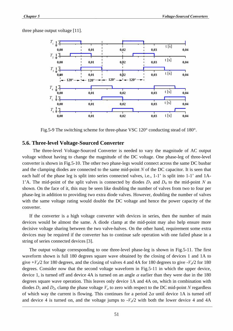
Chapter 5 Voltage-Sourced Converters
51
three phase output voltage [11].
0,00 0,01 0,02 0,03 0,0401
0,00 0,01 0,02 0,03 0,0401
0,00 0,01 0,02 0,03 0,0401
0,00 0,01 0,02 0,03 0,0401
0,00 0,01 0,02 0,03 0,0401
0,00 0,01 0,02 0,03 0,0401
120°
t [s]
t [s]
120° 120° 120°
t [s]
T6
T5
T4
T3
T1
T2
t [s]
t [s]
t [s]
Fig.5-9 The switching scheme for three-phase VSC 120° conducting stead of 180°.
5.6. Three-level Voltage-Sourced Converter The three-level Voltage-Sourced Converter is needed to vary the magnitude of AC output
voltage without having to change the magnitude of the DC voltage. One phase-leg of three-level converter is shown in Fig.5-10. The other two phase-legs would connect across the same DC busbar and the clamping diodes are connected to the same mid-point N of the DC capacitor. It is seen that each half of the phase leg is split into series connected valves, i.e., 1-1’ is split into 1-1’ and 1A-1’A. The mid-point of the split valves is connected by diodes D1 and D4 to the mid-point N as shown. On the face of it, this may be seen like doubling the number of valves from two to four per phase-leg in addition to providing two extra diode valves. However, doubling the number of valves with the same voltage rating would double the DC voltage and hence the power capacity of the converter.
If the converter is a high voltage converter with devices in series, then the number of main devices would be almost the same. A diode clamp at the mid-point may also help ensure more decisive voltage sharing between the two valve-halves. On the other hand, requirement some extra devices may be required if the converter has to continue safe operation with one failed phase in a string of series connected devices [3].
The output voltage corresponding to one three-level phase-leg is shown in Fig.5-11. The first waveform shown is full 180 degrees square wave obtained by the closing of devices 1 and 1A to give +Vd/2 for 180 degrees, and the closing of valves 4 and 4A for 180 degrees to give -Vd/2 for 180 degrees. Consider now that the second voltage waveform in Fig.5-11 in which the upper device, device 1, is turned off and device 4A is turned on an angle α earlier than they were due in the 180 degrees square wave operation. This leaves only device 1A and 4A on, which in combination with diodes D1 and D2, clamp the phase voltage Va to zero with respect to the DC mid-point N regardless of which way the current is flowing. This continues for a period 2α until device 1A is turned off and device 4 is turned on, and the voltage jumps to -Vd/2 with both the lower device 4 and 4A

Chapter 5 Voltage-Sourced Converters
52
turned on and both upper devices 1 and 1A are turned off and so on. Of course, angle α is variable, and the output voltage Va is made up of 180 2σ α° = ° − ° square waves. This variable period, σ, per half-cycle potentially allows the voltage Va to be independently variable with potentially a fast response. It is seen that the devices 1A and 4A are turned on for 180 degrees during each cycle devices 1 and 4 are turned on for 180 2σ α° = ° − ° during each cycle, while D1 and D2 conduct for 2 180α σ° = ° − each cycle. The converter is referred to as three-level because the DC voltage has three levels, i.e. / 2, 0, / 2d dV V− + [3].
1′
1A′
4′
4 A′
1A
1
4
4A
D1
D4
N
+Vd/2
-Vd/2
ai
Fig.5-10 One phase-leg of a three-level converter.
5.6.1. Pulse width modulation (PWM) for Three Level Converter In some two-level or multilevel converters, there is only one turn-on turn-off per device per
cycle. In these converters, the AC output voltage can be controlled by varying the width of the voltage pulses and/or the amplitude of the DC bus voltage. Another approach is to have multipulses per half-cycle and to vary the width of the pulses to vary the amplitude of the AC voltage. The principle reason for doing so is to be able to vary the AC output voltage and to reduce the low-order harmonics as will be explain here briefly. It goes without saying that more pulses means more switching losses, so that gains from the use of PWM have to be sufficient to justify the increase in switching losses. There are also resonant PWM converter topologies that incorporate current-zero type soft switching in order to reduce the switching losses. Such converters are being increasingly utilized in some low power applications, but with the known topologies they have not been justifiable at high power levels due to higher equipment cost [3].

Chapter 5 Voltage-Sourced Converters
53
Fig.5-12. shows the PWM output voltage waveform corresponding to a PWM frequency of three times the main frequency: The first waveform shows the control signals, similar to those in Fig.5-12. The second waveform is the phase a to DC neutral voltage vaN. It is seen that it has one notch in the centre of each half-cycle. The third waveform is vbN, the output voltage of phase b to DC neutral voltage, which is obviously the same as vaN, except the delay is 120 degrees. Subtracting vaN from vbN gives the phase-to-phase vab, as shown by the fourth waveform. This shows two notches resulting from the crossing of control signals.
-Vd/2
+Vd/2
Va
4,4A
180°
1,1A1,1A
4,4A
σ1,1A 2α
3,3A
1A,4A
1,1A
Va-Vb
Vb
Vd
-Vd
+Vd/2
5,5A3A,5A
Va
Fig.5-11 Operation of thee-level converter, output AC voltage.
The next waveform is that of the vaN, the voltage between the floating neutral n of a wye-connected floating secondary and the DC neutral. This is obtained by adding and averaging the three AC voltages, vaN, vbN, and vcN, (vcN not shown). Subtracting vnN from vaN gives the last waveform shown in Fig.5-12, that of the transformer phase-to-neutral voltage. Because of the half-wave symmetry, all the AC waveforms are free from even harmonics. Waveforms vab and van are triplen harmonics and the van lags vab by 30 degrees. As explained earlier, combining these two waveforms through separate wye and delta transformers will result in 12-pulse converter, which will have adequate flexibility of rapid AC voltage control without having to change the DC voltage level. The control of the DC voltage can then be optimized for other considerations. The pulses are wider in the middle of each half sine wave compared to the ends of the half sine wave [3], [11].
5.7 Summary
The VSC is an important element in FACTS applications and it have the following advantages which can be summarized as follows:
• Continuous operation, compensation, and control for reactive power requirements and voltage control/ stability applications
• Rapid and continuous response characteristics for smooth dynamic control.
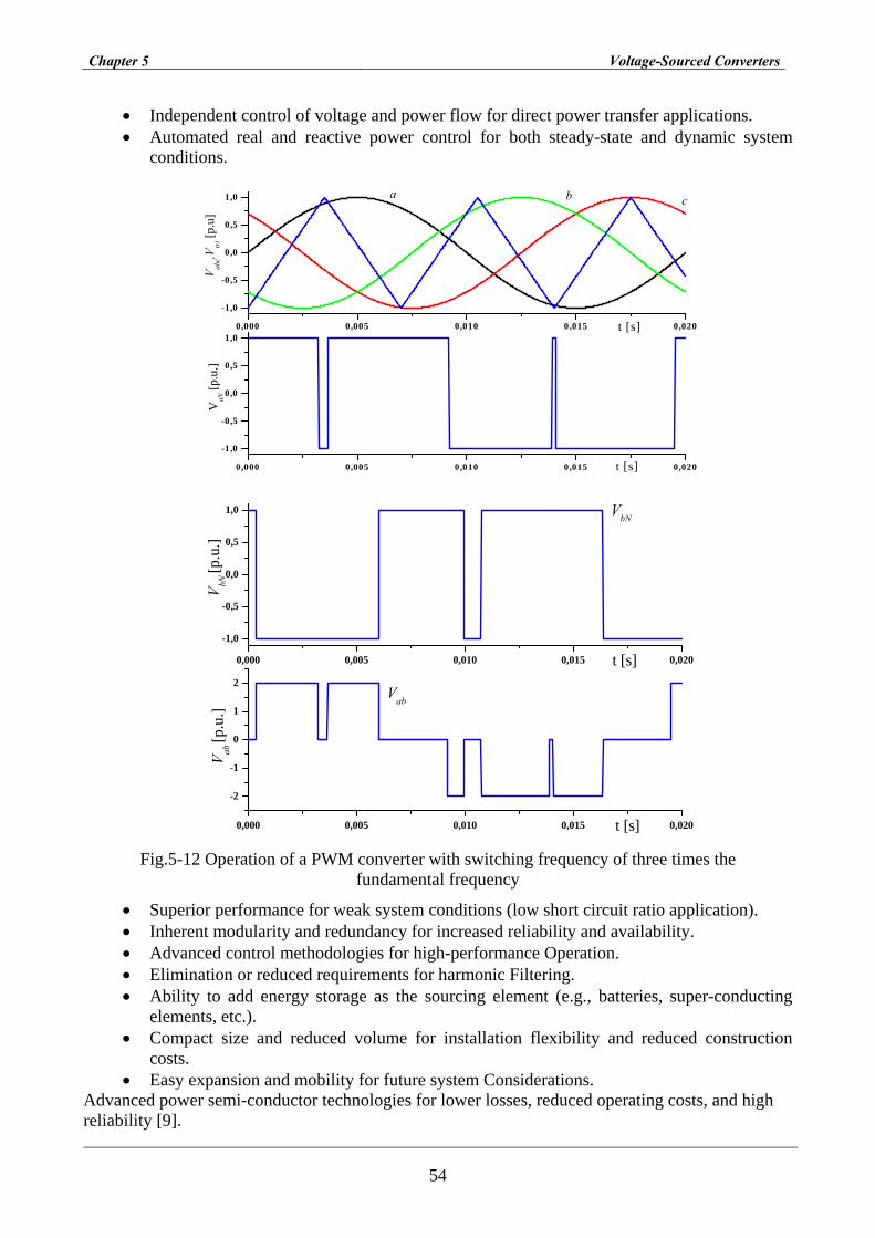
Chapter 5 Voltage-Sourced Converters
54
• Independent control of voltage and power flow for direct power transfer applications. • Automated real and reactive power control for both steady-state and dynamic system
conditions.
0,000 0,005 0,010 0,015 0,020
-1,0
-0,5
0,0
0,5
1,00,000 0,005 0,010 0,015 0,020
-1,0
-0,5
0,0
0,5
1,0 cb V
aN [p
.u.]
t [s]
a V
abc,V
tri [p
.u]
t [s]
0,000 0,005 0,010 0,015 0,020
-2
-1
0
1
2
0,000 0,005 0,010 0,015 0,020
-1,0
-0,5
0,0
0,5
1,0
Vab
t [s]
Vab
[p.u
.]
VbN
t [s]
VbN
[p.u
.]
Fig.5-12 Operation of a PWM converter with switching frequency of three times the
fundamental frequency
• Superior performance for weak system conditions (low short circuit ratio application). • Inherent modularity and redundancy for increased reliability and availability. • Advanced control methodologies for high-performance Operation. • Elimination or reduced requirements for harmonic Filtering. • Ability to add energy storage as the sourcing element (e.g., batteries, super-conducting
elements, etc.). • Compact size and reduced volume for installation flexibility and reduced construction
costs. • Easy expansion and mobility for future system Considerations.
Advanced power semi-conductor technologies for lower losses, reduced operating costs, and high reliability [9].

Chapter 6 Current-Sourced Converter and Self- and Line-Commutated
55
6 Current-Sourced Converter and Self- and Line-Commutated
6.1 Introduction and basic concept of Current-Sourced Converter
A Current-Sourced Converter is characterised by the fact the DC current flow is always in one direction and power flow reverses with the reversal of the DC voltage. In this respect, it differs from the Voltage-Sourced Converter in which the DC voltage always has one polarity and the power reversal takes place with reversal of the DC current. Fig.6-1 conveys the difference between the current sourced and the voltage sourced converter. In Fig.6-1(a), the converter box for Voltage-Sourced Converter is symbolically shown with a turn-off device with a reverse diode, whereas the converter box for the Current-Sourced Converter is shown without a specific type device in Fig.6-1(b). This is because the Voltage-Sourced Converter requires turn-off devices with reverse diodes, the Current-Sourced Converter may be based on diodes, conventional Thyristors or the turn-off devices.
Id
dc power
Reactive power
Vd
Active power
(a)
Id
dc powerReactive power
Vd
Active power
or or
or
or
(b)
Fig.6-1 Voltage-sourced and Current-Sourced Converter concepts: (a) voltage sourced converter; (b) Current-Sourced Converter.
There are three principle types of Current-Sourced Converter as demonstrated in Fig.6-2: • Diode converter, which is shown in Fig.6-2(a), which simply converts AC voltage to DC
voltage. It utilizes AC system voltage for commutation of DC current from one valve to another. Obviously the diode-based line-commutating converter just converts AC power to DC power without control and also in doing consumes some reactive power on the AC side.
• Line-commutated converter based on conventional thyristors (with gate turn-on but without gate turn-off capability), shown in Fig.6-2(b) and it utilizes an AC system voltage for commutation of the current from one valve to another. This converter can convert and control active power in either direction, but in doing so consumes reactive power on the AC side. It can not supply reactive power to the AC system.
• Self-commutated converter, which is shown in Fig.6-2(c), is based on turn-off devices (GTO’s, MTO’s, IGCT’s, IGBT’s, etc.). Here the commutation of current from valve to valve takes place with the device turn-off action and provision of AC capacitors to facilitate

Chapter 6 Current-Sourced Converter and Self- and Line-Commutated
56
transfer of current from valve to valve. In a Voltage-Sourced Converter the commutation of the current is supported by a stiff DC bus with a DC capacitor. In a self-commutated Current-Sourced Converter, the AC capacitors provide a stiff AC bus for supplying the fast changing current pulses needed for the commutation. A way from its capability of controlled flow in either direction, this converter (like the Voltage-Sourced Converter) can also supply or consume controlled reactive power. However, it is interesting to note that even though the converter can supply reactive power, sources of reactive power, i.e. capacitors and AC filters are needed in any case. One advantage of the converters with turn-off devices (self-commutating converters) is that they offer greater flexibility including the PWM mode of operation [3].
dc current
dc power
Filters & capacitors
dc voltage
Active & reactivepower
(a)
dc current
dc power
Filters & capacitors
dc voltage
Active power
Reacctive power
(b)
dc current
dc power
Filters
dc voltage
Active power
Reacctivepower
Capacitors (c)
Fig.6-2 Types of Current-Sourced Converter, (a) diode rectifier; (b) Thyristor line-commutated converter, (c) self-commutated converter.
It is worth mentioning have that when the converters are based on turn-off devices, the Voltage-Sourced Converters are preferred over the Current-Sourced Converters. In fact, none of the converter-based controllers described here are based on Current-Sourced Converters. However, with evolution in device characteristics and functional details of the converters, this situation may change in the future. Therefore, the Current-Sourced Converters with turn-off devices are not discussed in detail here. When reactive power management is not a problem, where controlled reactive power supply is not required and the active power consumed by the converters can be

Chapter 6 Current-Sourced Converter and Self- and Line-Commutated
57
supplied from the system capacitors and/or filters, the line-commutated converters have decisive economic advantages over self-commutated converters. For conversion AC to DC and DC to AC, in HVDC transmission, line commutated converters are used almost exclusively where reactive power is managed through capacitors, filters and the power system. The converters for superconducting storage can be Current-Sourced Converters since the superconducting reactor it self is a current source. Also, the DC power supply for storage means, can be Current-Sourced Converters, in order to drive Voltage-Sourced Converter-based phase-angle regulators. The economic advantage of conventional Thyristor-based converters arises from the fact that on a per device basis thyristors can handle two to three times the power than the next most powerful GTO’s, IGCT’s, MTO’s, etc.
Other converters which are variations of the basic types above of Current-Sourced Converters, such as thyristors converters with artificial commutation, resonant converters and hybrid converters, are not discussed here. Since the DC voltage in a Current-Sourced Converter can be in either direction, the converter valve must have both forward and reverse blocking capability. The conventional thyristors are usually made as symmetric devices. They have both the forward and reverse blocking capability. This is because they are on the other hand easier and cheaper to make and can be made with peak blocking voltage as 12kV along with a high current carrying capability. On the other hand, the turn-off devices have a high on-state forward voltage drop when they are made symmetric devices. Given that the high production volumes of asymmetric turn-off devices dictated by the industrial market, it may be advantageous to connect an asymmetric turn-off device and a diode in series to get a symmetric devices combination. This results in higher forward voltage drop and losses. Based on this and on other aspect, such as fast-switching characteristics of IGBT’s, the industrial converter market has shifted very fast towards the PWM Voltage-Sourced Converter as discussed before [3].
6.2 Single-phase bridge rectifier
A single-phase bridge rectifier is presented in Fig.6-3. These types of rectifiers do not suffer from the problem of DC magnetization and low device and transformer utilization. They also offer higher DC output voltage for a given AC supply voltage. This is at the cost of lower efficiency, because there are two diode drops between the load voltages. The AC supply voltage is given in the following:
max max0
2sin( ), sin( ) ( )S dv V t V t d t Vπ
ω ω ωπ
= = =∫ (6-1)
where Vmax is the peak of the input AC voltage to the rectifier. The PRV (Peak Reverse Voltage) of each diode is Vmax, not 2Vmax, as in the case of the centre-tapped rectifier [12].
6.3 Three-phase bridge rectifier A three-phase bridge rectifier (diode rectifier) is presented in Fig.6-4. In this bridge rectifier, the diodes 1, 3 and 5, whichever have a more positive voltage at its anode, conduct respectively. Similarly, diodes 2, 4 and 6, whichever have a more negative voltage at its cathode, return the load current. With the numbering of diodes as indicated in Fig.6-5 the conduction patterns are 12-23-34-45-56-61-12 for a positive voltage sequence a-b-c. For the negative voltage sequence a-c-b, the patterns are 16-65-54-43-32-21-16.

Chapter 6 Current-Sourced Converter and Self- and Line-Commutated
58
R
LVd
iLi1
iP
vS
D2
D2 D3
D4
Fig.6-3 Diode bridge rectifier.
When any of the diodes connected with the top (+ve) rail conducts, the potential of the rail is the corresponding AC line voltage When any of the diodes connected with the bottom (-ve) rail conducts, the potential of the rail is the corresponding AC line voltage. When any of the diodes connected with the bottom (-ve) rail conducts, the potential of the rail is the corresponding AC line voltage.
R
D1 D3
D6D2D4
n
ia
ib
ic
van
vbn
vcn
Vd
iL
vO
L
Load
D5
Fig.6-4 A three-phase bridge rectifier.
The voltage across the load is the difference between the +ve and the -ve rail potentials. Assuming that the load current is continuous (i.e., non zero) at all times, each diode conducts for 120° in each half cycle of the AC waveform, followed by 240° of non conduction. The output voltage waveform, the Vd can be given by the following Equation:
/ 6
max max/ 6
6 3cos( ) ( )2d l l l lV V t d t V
π
πω ω
π π− −−= =∫ (6-2)
where Vmaxl-l is the peak value of the line-line voltage [12].
6.4 Phase-controlled AC-DC converters The controlled AC-DC rectifier circuits with thyristors are commonly used in applications
requiring continuously variable DC supplies from a few kilowatts to several hundreds or thousands

Chapter 6 Current-Sourced Converter and Self- and Line-Commutated
59
of kilowatts. The thyristor switch may be viewed as a controlled diode which is turned on by the gate current; a few milliamp or at least amps will turn even the largest device on, when its anode to cathode voltage is positive. Once the thyristor is fired or triggered on. The Thyristor will turn off when the anode current falls, brought about by the AC source and load, below a threshold close to zero. The thyristors in an AC rectifier, therefore, must be triggered synchronously with the AC supply each cycle, by means of a gate control circuit which is interfaced with the AC mains. The firing angle α, is normally defined to be the angle for which the output DC voltage is maximum. The thyristors are triggered with short (a few volts, mA level) pulses, one time in each AC cycle, as shown in Fig.6-5. These pulses are obtained from a firing controller circuit which is synchronised with the AC mains. In some converter circuits, the firing pulses for each thyristor are maintained for the intended duration of conduction for the Thyristor [13].
-10 V
+10 V
-10 VFiringControlCircuit
Load
max sin( . )V tω
Fig.6-5 The rectifier and the phase controller for a half-wave converter.
6.4.1 Single-phase, fully-controlled bridge rectifier
This diagram of this converter is presented in Fig.6-6. Assuming continuous conduction, the DC output voltage is given by:
maxmax
21 sin( ) ( ) cosdVV V t d t
π α
αω ω α
π π+
= =∫ (6-3)
where Vmax is peak value of the input line-line voltage. For the same DC output voltage, the input AC voltage is now half that of the CT rectifier. This converter operates in quadrants one and four. There are now two device drops (about 3V) between the transformer and the load. Also, the transformer secondary current is bi-directional and its phase angle with respect to the AC supply voltage to the converter is roughly given by the firing angle α. With continuous conduction, each thyristor conducts for 180° in each cycle. This 2-pulse converter operates in two quadrants [13].
6.5 Three-phase fully controlled bridge converters Three-phase fully controlled bridge converter circuit is presented in Fig.6-7, the thyristor
connected with the positive DC rail, which has the most positive voltage at its anode, conducts

Chapter 6 Current-Sourced Converter and Self- and Line-Commutated
60
when triggered. The thyristors connected with the negative DC rail, the thyristor with the most negative voltage at its cathode returns the load current, if triggered. It will be useful to see the numbering of the thyristors and the sequential triggering of the thyristors. Commutation of the load current from one thyristor to the next occurs at the firing instant, when the incoming thyristor reverse biases the previously conducting thyristor, as presented in Fig.6-7.
R
LVd
iLi1
iP
vS
T2
T1 T3
T4
Fig.6-6 A single-phase fully-controlled bridge rectifier (thyristor with p=2).
Having established the conduction times of the thyristors, the output DC voltage waveform is determined by the difference of potentials of the positive and negative rails. For continuous conduction, the potentials of each rail are known at all times from the firing angles and the input AC voltages, regardless of the load. Assuming continuous conduction, the output voltage Vd can be formulated as:
2 /3 maxmax/3
33 sin( ) ( ) cosl ld l l
VV V t d tπ α
π αω ω α
π π+
−−+
= =∫ (6-4)
This converter operates in quadrants 1 and 4, developing both positive and negative polarity DC output voltage. For firing angles 0 90α° ≤ ≤ ° , the converter operates in quadrant 1 (giving positive output power, i.e., rectifier operation) and for90 180α° ≤ ≤ ° , the operation is in quadrant 4 (giving negative output power, i.e., inverter operation). Operation in quadrant 4 is of course possible only when the load includes an active DC source, able to supply power into the AC supply circuit [13].
R
T1 T3
T6T2T4
n
ia
ib
ic
van
vbn
vcn
Vd
iL
vO
L
Load
T5
Fig.6-7 Three-phase, fully-controlled bridge converter circuit.
Chapter 6 Current-Sourced Converter and Self- and Line-Commutated
61
6.6 Current-Sourced Converter with turn-off devices The Current-Sourced Converter with turn-off devices is also referred to as current-stiff converter.
As mentioned previously, the turn-off devices must have the reverse withstand voltage capability (symmetric device) or have diodes in series if they are asymmetric devices.
In the Current-Sourced Converter with the conventional thyristor which discussed before, the operation of the converter is limited to the third and fourth quadrant (lagging power factor). This is because thyristors don’t have turn-off capability and the DC current has to be commutated from valve to another while the anode-cathode voltage of the incoming valve is still positive. Also, such a converter needs an AC voltage source for commutation.
In the Voltage-Sourced Converters which is discussed in chapter5, there is a DC capacitor, which facilitates rapid transfer of current from an outgoing turn-off valve to the opposite valve in a phase-leg, irrespective of the direction of the AC current. The capacitor is assumed to be large enough to handle alternate charging and discharging without substantial change in the DC voltage. With turf-off capability, the valves can be turned off as well. However, turn-off devices in order to turn off still require an alternate path for rapid transfer of the current. Otherwise, they will have to dissipate a large amount of energy to turn off the current in an inductive circuit. It can be visualized that if the capacitors are placed between the phases, on the AC side of the valves as presented in Fig.6-8(a). The capacitors can facilitate fast transfer of the current from the outgoing turn-off valve to the incoming valve.
The commutation of the current from the valve 1 to the valve 3 is illustrated in Fig.6-8(b). Given low inductance of the AC shunt capacitor and the bus connection, the transfer (commutation) is fast and there is no commutation angle to speak of as far as the valves are concerned. Actually, with respect to the turn-on di/dt limit of the devices, the inductance of the capacitors and the bus connections can be duly exploited. Also it is to be noted, that a valve turns off, valve 1 in Fig.6-8(b), its rate of rise of the voltage is cushioned by the AC capacitor. It is a complex and important matter in terms of the devices losses and snubber requirements. These capacitors need to handle a sustained alternating charge/discharge current of the converter valves. Unlike the line commutated converter using conventional thyristors, this converter with turn-off valves can operate even with leading power factor and does not need a pre-existing AC voltage for commutation. It can in fact operate as an inverter into passive or an active AC system.
Fig.6-8(c) shows the anode-bus current connected to the anode side of valves 1, 3, and 5 and transfer of this incoming DC current from valve 1 to 3, to 5, to 1, etc., in a closed three-valve sequence in a three-phase converter. Similarly shown are the cathode bus current, the outgoing DC current, and how it transfers from valve 2, to 4, to 6, to 2 etc., in a closed three-valve sequence. The two sequences are phase shifted by 60 degrees and they are together from a three-phase, full-wave bridge converter. Consequent injected AC current in the three phase as it is shown in Fig.6-8(c), which is same as for the conventional thyristor converter when neglecting commutation angle, see Fig.6-8(b).
The currents are injected without the support of the AC system voltage, and therefore, the phase angle and the frequency of this injected AC current can be controlled. To understand the operation of this converter, it is appropriate to visualize it as an AC current generator connected to an AC system, which is front-ended with AC capacitor as presented in Fig.6-8(d). The AC side

Chapter 6 Current-Sourced Converter and Self- and Line-Commutated
62
fundamental and harmonics are a function of the AC system and the injected current. A DC side converter voltage will also have harmonics.
or
4 6Id
1 3 5
2
AC system or passive load
(a) 6-pulse converter
1 3
2
(b) Commutation process.
Id 1 3 5 1
6426
Cathode bus current
Anode bus current
14
1
3
5
66
2 2
ia
ib
ic
(c) Current waveforms.
(d) System interface.
Fig.6-8 Self-commutating current-sourced converter: (a) six-pulse converter, (b) commutation process, (c) current waveforms, and (d) system interface.

Chapter 6 Current-Sourced Converter and Self- and Line-Commutated
63
Various PWM concepts, which like e.g. those discussed in Chapter5, are applicable to the current-sourced converters; the advantage of the PWM operation is that the commutation capacitor size will decrease [3].
6.7 Current-Sourced versus Voltage-Sourced Converters
There are some advantages and disadvantages of current-sourced versus voltage-sourced converters:
• Diode-based converters are the lowest cost converters, if control of active power by the converter is not required.
• If the leading reactive power is not required, then a conventional thyristor-based converter provides a low-cost converter with active power control. It can also serve as controlled lagging reactive power load (like a thyristor-controlled reactor).
• The current-sourced converter does not have high short-circuit current, as does the voltage-sourced converter. For current-sourced converters, the rate of rise of fault current during external or internal faults is limited by the dc reactor. For the current-sourced converters, the capacitor discharge current would rise very rapidly and can damage the valves.
In a current-stiff converter, the valves are not subject to high dv/dt, due to the presence of the ac capacitors
• AC capacitor required for current-stiff converters can be quite large and expensive, although their size can be decreased by adoption of PWM topology. In general the problem of satisfactory interface of current-sourced converters with the ac system is more complex.
• With the presence of capacitors, which are subjected to commutation charging and discharging, this converter will produce harmonic voltages at a frequency of resonance between the capacitors and the ac system inductance. Adverse effects of this can be avoided by sizing the capacitors such that the resonance frequency does not coincide with characteristic harmonics.
• The harmonics as well as the presence of dc reactor can result in over-voltages on the valves and transformers.
Widespread adoption of asymmetrical devices, IGBT’s and GTO’s, as the devices of choice for lower on-state losses, has made current-sourced converters a favourable choice when turn-off capability is necessary. The devices market is generally driven by high-volume industrial applications and as a result symmetrical turn-off devices by high-voltage rating and required operating characteristics may not be readily available until the volume of the FACTS market increases [3].

Chapter 7 Snubber Circuits
64
7 Snubber Circuits
7.1 Introduction When a power electronic converter stresses a power semiconductor device beyond its ratings,
there are two basic ways of relieving the problem. Either the device can be replaced by one whose ratings exceed the stresses or a snubber circuit can be added to the basic converter to reduce the stresses to safe levels. The final choice will be a trade-off between cost and availability of the semiconductor device with the required electrical ratings compared to the cost and the additional complexity of using a snubber circuit. The power electronics circuit designer must be familiar with the design and operation of basic snubber circuits in order to make the comparison trade-off. This chapter discusses the fundamentals of the snubber circuits commonly used in power electronics to reduce electrical stresses on power semiconductor devices.
7.2 Function and types of snubber circuits The function of a snubber circuit is to reduce the electrical stresses placed on a device during
switching by a power electronic converter to levels that are within the electrical ranges of the devices. More explicitly, a snubber circuit reduces the switching stresses to safe level by:
• Limiting the voltages applied to a device during turn-off transients. • Limiting the device currents during the turn-on transients. • Limiting the rate of rise (di/dt) of the current through the devices at turn-on. • Limiting the rate of rise (dv/dt) of the voltage across the devices at turn-off or during
reapplied forward blocking voltage. • Shaping of the switching trajectory of the device as it turns on and off. From the circuit topology perspective, there are three broad classes of snubber circuits. These
classes include: • Unpolarized series RC snubbers used to protect diodes and thyristors by limiting the
maximum voltage and dv/dt at reverse-recovery. • Polarized RC snubbers. These snubbers are used to shape the turn-off portion of the
switching trajectory of controllable switches, to clamp voltage applied to the devices to safe levels, or to limit dv/dt during device turn-off.
• Polarize RL snubbers. These snubbers are used to shape the turn-on switching trajectory of controllable switches and /or to limit di/dt during device turn-on.
Switching stresses are also controlled by utilizing a board class of power electronic converter circuit termed resonant or quasi-resonant converters. It must be emphasized that snubbers are not a fundamental part of power electronic converter circuit. The snubber circuit is an additional part to the basic converter, which is added to reduce the stresses on an electrical component. Usually, in a power semiconductor device, snubbers may be used singly or in combination depending on the requirements. As mentioned before, the additional complexity and the cost added to the converter circuit by the presence of the snubber must balance against the benefits of limiting the electrical stresses on critical circuit components [8].

Chapter 7 Snubber Circuits
65
7.3 Diode snubber Snubbers are needed in diode circuits to minimize over-voltage occurring in circuits such as the
step-down converters in Fig.7-1(a) and the other diode applications like in FACTS systems, due to the stray or leakage inductance in series with the diode and snap-off the diode reverse recovery current at the turn-on switch T (see Fig.7-1(a)). The analysis of the snubber circuit that will protect the diode will be based on this step-down converter circuit, where Lσ is the stray inductance. It is shown later that for the purpose of snubber analysis, this circuit is an equivalent circuit for almost any converter where diodes are used. An RS-CS snubber is commonly used across the diode for over-voltage protection as shown in Fig.7-1(a).
To simplify the analysis, the diode reverse recovery current is assumed to snap off instantaneously as shown in Fig.7-1(b). The load is inductive and it is assumed that the load current I0 is constant during the switching transient [8], [14], and [15].
CS
Df
RS
Vd
vD
Dfi+
+
--
oI
T
Lσ Li σ
Irr
iDf(t)
VDf(t)
t
t
IO
dVdidt Lσ
= −
Vd
LdiL
dtσ
σ
(a) (b) Fig.7-1 (a) A step-down converter circuit with stray inductance and a snubber circuit for the
free-wheel diode, (b) the Diode reverse-recovery current and diode voltage.
7.3.1 Capacitive snubber Although the capacitive snubber (RS = 0) is not used in practice, it provides an easily analyzed
starting point for analysis that illustrates the basic concept. In obtaining an equivalent circuit, the switch in Fig.7-2(a) is assumed to be ideal, which results in a worst-case analysis of the circuit. Treating the instant of diode snap-off at the peck reverse recovery current Irr (Repetitive reverse current) at t =0, the initial inductor current in the equivalent circuit of Fig.7-2(c), is Irr and the initial snubber capacitor voltage is zero. To establish a baseline circuit, the snubber resistance RS is assumed to be zero as in Fig.7-2(b), the capacitor voltage which is the negative of the diode voltage in this baseline circuit is given by:
0 0cos( ) sin( )SC d d rr
S
Lv V V t I tC
σω ω= − + (7-1)
where
0 1/( )SL Cσω = (7-2)

Chapter 7 Snubber Circuits
66
Introducing a baseline capacitance baseC given by:
2][d
rrbase V
ILC σ=
(7-3)
It is possible to express in Equation (7-1) as:
0 0[1 cos( ) sin( )]S
baseC d
S
Cv V t tC
ω ω= − + (7-4)
Either by a time derivative or a phasor approach, the maximum value of vCs in Equation (7-4) can be estimated as:
,max [1 1 ]S
baseC d
S
Cv VC
= + + (7-5)
The waveform and inductor current are shown in Fig.7-2(c), for S baseC C= . In this case the maximum reverse-diode voltage is the same as VCs,max calculated from Equation (7-5). For small value of CS, the maximum diode voltage becomes excessive [8], [14], and [15].
7.3.2 Effect of adding a snubber resistor When the diode snubber resistor RS is included, the equivalent circuit for the snubber becomes
as shown in Fig.7-3. In analyzing this modified circuit the instant of diode snap-off is treated as 0t = , and the initial inductor current is Irr and the initial capacitor voltage is zero. The differential equation governing the behavior of the diode voltage is:
2
2f f
f
D DS S S D d
d v dvL C R C v V
dt dtσ + + = (7-6)
The boundary conditions are: (0 )fD rr Sv I R+ = − and:
2(0 )fD S d rr Srr
S
dv R V I RIdt C L Lσ σ
+
= − − −
The solution of the Equation (7-6) is given by:
( ) cos( )cos( )f
trrD d
S
L Iv dt V e tC
ασαω φ γ
φ= − − × − − (7-7)
where 2
-1 -120
/ 21 ; ; = tan ( ) ; and =tan ( ) 2
S d rr S
rr
R V I RL I
αα
α α σ
ωαω α φ γω ω ω α
−= − = (7-8)
The time mt t= at which the voltage given by the Equation (7-7) is a maximum can be found by setting the derivative /
fDdv dt equal to zero and solving for time. Doing these yields: / 2 0mt
α
φ γ πω
+ −= ≥ (7-9)

Chapter 7 Snubber Circuits
67
CS
RS
Vd
+
_
vCs
+
_
Cathode
AnodeDiode
snap-off
rrICi
Li σ
Lσ
CSVd
+
_vCs
+
_T
Li σ
Lσ
(a) (b)
,maxCsV
ddiL Vdtσ =
Liσ
Irr
Vd
vCs
t0
(c)
Fig.7-2:(a) Equivalent circuit of the step-down converter at the instant of diode reverse-recovery current snap-off (b) the simplification that results when the snubber resistance is zero and (c)
The voltage and current waveforms for RS = 0 and CS = Cbase.
CS
RS
Vd
+
_
+
_
VDf(t)
Lσ
Fig.7-3 Equivalent circuit with snubber resistance RS.
Substituting mt t= into the Equation (7-7) yields the maximum reverse recovery voltage across the diode as:
2max 1 1 0.75( ) e mtbase S S
d S base base
V C R RV C R R
α−⎧ ⎫⎪ ⎪= + + + −⎨ ⎬⎪ ⎪⎩ ⎭
(7-10)
In the Equation (7-10), the baseline capacitive Cbase is given by the Equation (7-3) and the resistance Rbase is given by:
dbase
rr
VRI
= (7-11)
Typical circuit waveforms for t > 0 are shown in Fig.7-4 as an example, for S baseC C= , in these waveforms, the oscillations damped by RS, and the maximum diode voltage depends on the values of RS and CS which are used. For selected values of CS, the maximum diode voltage varies with RS

Chapter 7 Snubber Circuits
68
as an example for the plotted curve in Fig.7-6 as a function of RS /Rbase. It can be seen that for this value of CS, there is an optimum value of 1.3S opt baseR R R= = that minimizes Vmax. A snubber design monogram is shown in Fig.7-6, where the optimum snubber resistance and corresponding Vmax are plotted as a function of CS. In this monogram all quantities are normalized.
Fehler! Es ist nicht möglich, durch die Bearbeitung von Feldfunktionen Objekte zu erstellen.
Fig.7-4 The current and the voltage waveforms after diode snaps-off at t = 0.
The energy loss in the resistor RS is given by the following Equation: 2 21 [ ]
2R rr S dW L I C Vσ= + (7-12)
where, WR is normalized with respect to ( 21/ 2( )rrL Iσ , the peak energy stored in the leakage inductance as the diode snaps off, is also plotted in Fig.7-6. At the end of the current oscillation, the energy stored in CS is equals to:
21/ 2SC S dW C V= (7-13)
This is dissipated in the diode at the next turn-on of the diode. Assuming a instantaneously turn-on of the diode, the total energy dissipated in the diode and the snubber resistance is given by the following:
2 2 2tot
1 1[ ] (1 2 )2 2S
SR C rr S d rr
base
CW W W L I C V L ICσ σ= + = + = + (7-14)
The normalized Wtot is also plotted in Fig.7-6 as a function of the normalized CS. It can be seen from Fig.7-5 that the maximum voltage decreases only slightly by increasing CS beyond Cbase. However, the total energy dissipation increases linearly with CS. Therefore, a snubber capacitor with CS in a range close to Cbase would be used. Once CS has been selected, RS = Ropt can be obtained directly from Fig.7-6. In this analysis, it is assumed that the reverse-recovery current of the diode snaps off instantaneously. In practice, the diode reverse-recovery current can be assumed to decay exponentially. This can be accommodated in the equivalent circuit in Fig.7-2 by adding a time-varying current source. This analysis can be carried out by computer simulation, and the result shows that the snubber design remains essentially the same [8].
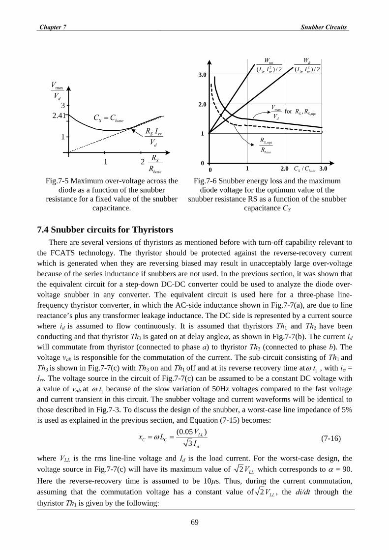
Chapter 7 Snubber Circuits
69
2.41
1 2
1
3
S
base
RR
max
d
VV
S baseC C=
S rr
d
R IV
1
1
2.0 3.0
2.0
3.0
00
tot2( ) / 2rr
WL Iσ
2( ) / 2R
rr
WL Iσ
/S baseC C
,optS
base
RR
max,opt for ,S S
d
V R RV
Fig.7-5 Maximum over-voltage across the
diode as a function of the snubber resistance for a fixed value of the snubber
capacitance.
Fig.7-6 Snubber energy loss and the maximum diode voltage for the optimum value of the
snubber resistance RS as a function of the snubber capacitance CS
7.4 Snubber circuits for Thyristors There are several versions of thyristors as mentioned before with turn-off capability relevant to
the FCATS technology. The thyristor should be protected against the reverse-recovery current which is generated when they are reversing biased may result in unacceptably large over-voltage because of the series inductance if snubbers are not used. In the previous section, it was shown that the equivalent circuit for a step-down DC-DC converter could be used to analyze the diode over-voltage snubber in any converter. The equivalent circuit is used here for a three-phase line-frequency thyristor converter, in which the AC-side inductance shown in Fig.7-7(a), are due to line reactance’s plus any transformer leakage inductance. The DC side is represented by a current source where id is assumed to flow continuously. It is assumed that thyristors Th1 and Th2 have been conducting and that thyristor Th3 is gated on at delay angleα, as shown in Fig.7-7(b). The current id will commutate from thyristor (connected to phase a) to thyristor Th3 (connected to phase b). The voltage vab is responsible for the commutation of the current. The sub-circuit consisting of Th1 and Th3 is shown in Fig.7-7(c) with Th3 on and Th1 off and at its reverse recovery time at 1tω , with iσ = Irr. The voltage source in the circuit of Fig.7-7(c) can be assumed to be a constant DC voltage with a value of vab at 1tω because of the slow variation of 50Hz voltages compared to the fast voltage and current transient in this circuit. The snubber voltage and current waveforms will be identical to those described in Fig.7-3. To discuss the design of the snubber, a worst-case line impedance of 5% is used as explained in the previous section, and Equation (7-15) becomes:
(0.05 )3
LLC C
d
Vx LI
ω= = (7-16)
where VLL is the rms line-line voltage and Id is the load current. For the worst-case design, the voltage source in Fig.7-7(c) will have its maximum value of 2 LLV which corresponds to α = 90. Here the reverse-recovery time is assumed to be 10µs. Thus, during the current commutation, assuming that the commutation voltage has a constant value of 2 LLV , the di/dt through the thyristor Th1 is given by the following:

Chapter 7 Snubber Circuits
70
2 LL
C
Vdidt L
= (7-17)
and therefore,
6 0.090.1
LL rr drr rr d
LL
V t IdiI t Idt V
⎛ ⎞= = =⎜ ⎟⎝ ⎠
(5-18)
where trr = 10µs. As was discussed in the previous section, CS = Cbased is close to an optimum value. Relating to
Fig.7-7(c) and Fig.7-2(a) and the Equation (5-3) gives by the following Equation: 2
baserr
CLL
IC LV
⎛ ⎞= ⎜ ⎟
⎝ ⎠ (7-19)
Substituting Lc from the Equation (7-16) at ω = 377 and Irr from the Equation (7-18) into the Equation (7-19) yields:
( F) 0.6 /S base d LLC C I Vµ= = (7-20)
RS =Ropt can be obtained from Fig.7-6. Here, assuming the normalized 1.3S opt baseR R R= = , and the value 2 /base LL rrR V I= , it will give, using the Equation (7-18).
opt 1.3 2 / 20 /S LL rr LL dR R V I V I= = = (7-21)
In order to estimate the loss in each snubber, the voltage waveforms across a thyristor having a worst-case trigger angle of α = 90. It can be shown that the total energy loss in each snubber equals:
2snubber 3
LLSW C V= (7-22)
or using the Equation (7-20) gives: 6
snubber 1.8 10 d LLW I V−= × (7-23)
If the power of the three-phase converter kVA is S, then at 50Hz, each snubber has a power loss equals:
4snubber (in watts) 10P S−= (7-24)
A similar procedure can be followed for any value of trr and AC-line inductance. A conservative design may require CS to be big than Cbase, and therefore RS would be smaller than the value found above. In that case, the snubber losses would be higher since they are proportional to CS [8], [15], [31].
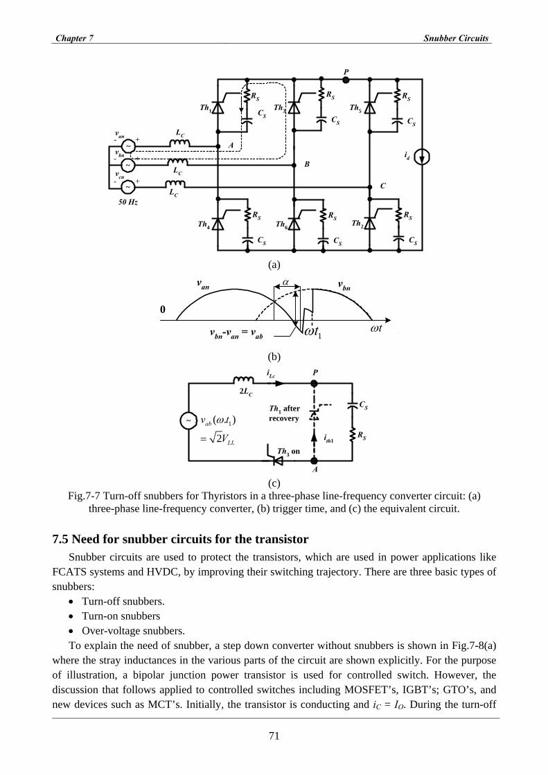
Chapter 7 Snubber Circuits
71
50 Hz
id
~
Th1 Th3 Th5
Th2 Th6 Th4
LC
LC
~
~
+
+
+-
-
-
vcn
vbn
van
RS
CS
RS
CS
RS
CS
RS
CS
RS
CS
RS
CS
A
B
C
P
LC
(a)
vbn-van = vab
van vbn
tω1tω
α
0
(b)
RS
CS
Th3 on
~
P
A
Th1 afterrecovery
2LC
1( . )
2ab
LL
v t
V
ω
=
iLc
ith1
(c)
Fig.7-7 Turn-off snubbers for Thyristors in a three-phase line-frequency converter circuit: (a) three-phase line-frequency converter, (b) trigger time, and (c) the equivalent circuit.
7.5 Need for snubber circuits for the transistor Snubber circuits are used to protect the transistors, which are used in power applications like
FCATS systems and HVDC, by improving their switching trajectory. There are three basic types of snubbers:
• Turn-off snubbers. • Turn-on snubbers • Over-voltage snubbers. To explain the need of snubber, a step down converter without snubbers is shown in Fig.7-8(a)
where the stray inductances in the various parts of the circuit are shown explicitly. For the purpose of illustration, a bipolar junction power transistor is used for controlled switch. However, the discussion that follows applied to controlled switches including MOSFET’s, IGBT’s; GTO’s, and new devices such as MCT’s. Initially, the transistor is conducting and iC = IO. During the turn-off
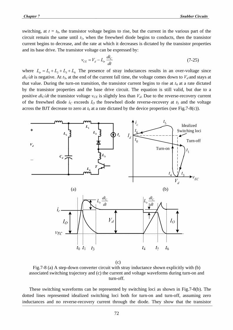
Chapter 7 Snubber Circuits
72
switching, at t = t0, the transistor voltage begins to rise, but the current in the various part of the circuit remain the same until t1, when the freewheel diode begins to conducts, then the transistor current begins to decrease, and the rate at which it decreases is dictated by the transistor properties and its base drive. The transistor voltage can be expressed by:
CCE d
div V Ldtσ= −
(7-25)
where 1 2 3 4L L L L Lσ = + + + The presence of stray inductances results in an over-voltage since diC/dt is negative. At t3, at the end of the current fall time, the voltage comes down to Vd and stays at that value. During the turn-on transition, the transistor current begins to rise at t4 at a rate dictated by the transistor properties and the base drive circuit. The equation is still valid, but due to a positive diC/dt the transistor voltage vCE is slightly less than Vd. Due to the reverse-recovery current of the freewheel diode iC exceeds IO the freewheel diode reverse-recovery at t5 and the voltage across the BJT decrease to zero at t6 at a rate dictated by the device properties (see Fig.7-8(c)).
Cd
Vd
+
_
L1
L5L2
L4
L3
T
Io
t1
t3t4
t5
t6
t0
Vd
Id
ic
vEC
Turn-off
IdealizedSwitching loci
Turn-on
(a) (b)
CdiLdtα
CdiLdtα
(c) Fig.7-8 (a) A step-down converter circuit with stray inductance shown explicitly with (b)
associated switching trajectory and (c) the current and voltage waveforms during turn-on and turn-off.
These switching waveforms can be represented by switching loci as shown in Fig.7-8(b). The dotted lines represented idealized switching loci both for turn-on and turn-off, assuming zero inductances and no reverse-recovery current through the diode. They show that the transistor

Chapter 7 Snubber Circuits
73
experiences high stresses at turn-on and turn-off when both its voltage and current are high simultaneously, thus causing a high instantaneous power dissipation. Moreover, the stray inductances result in over-voltage beyond Vd, and the diode reverse-recovery current causes beyond IO. If necessary, snubber circuits are used to reduce these stresses. An important assumption that simplifies the snubber circuit analysis is that the transistor current change linearly in time with a constant di/dt, which is only dictated by the transistor and its base drive circuit. Therefore, di/dt, which may be different at turn-on and turn-off, is assumed not to be affected by the addition of the snubber circuit. This assumption provides the basis for a simple design procedure for a laboratory prototype. The final design may be somewhat different depending on what is revealed by laboratory measurements on the prototype circuit [8], [16], [17], [31].
7.6 Turn-off snubber: The main aim of a turn-off snubber is to provide a zero voltage across the transistor in order to
avoid the turn-off problems. This can be approached by connecting a RCD network across the BJT as shown in Fig.7-10(a). Here, the stray inductances are ignored initially for ease of explanation. Prior to turn-off, the transistor current is IO and the transistor voltage is essentially zero. At turn-off in the presence of this snubber, the transistor current iC decreases with a constant di/dt and ( )O CI I− flows into the capacitor through the snubber diode DS. Therefore, for a current fall time of tfi, the capacitor current can be written as:
/ , 0 1 SC o fii I t t t= < < (7-26)
where iCs is zero prior to turn-off time at 0t = . The capacitor voltage, which is the same as the voltage across the transistor when DS is conducting, can be written as:
2
0
12S S
t oC CE C
S S fi
I tv v i dtC C t
= = =∫ (7-27)
The Equation (7-27) is valid during the current fall time so long as the capacitor voltage is less than or equal to Vd. The equivalent circuit that represents this condition is shown in Fig.7-10(b). The voltage and the current waveforms are shown in Fig.7-9(c) for three values of the snubber circuit capacitance CS [19], [20].
For a small value of capacitance, the capacitor voltage reaches Vd before the current fall time is over. At that time, the freewheel diode Df turns on and clamps the capacitor and the transistor to Vd and iCs drops to zero due to /
SCdv dt is equal to zero. The next sets of waveforms in Fig.7-9(c) are drawn for a value of CS = CS1, which causes the capacitor voltage to reach the Vd exactly at the current fall time tfi. In this case; the value of the capacitor CS1 can be calculated by substituting t = tfi and
SC dv V= in the Equation (7-27) and is given by:
1 2o f i
Sd
I tC
V= (7-28)
For large snubber capacitance with CS > CS1, the waveforms in Fig.7-9(c) show that the transistor voltage rises slowly and takes longer than tfi to reach Vd. Beyond tfi, the capacitor current equals IO and the capacitor and the transistor voltages rise linearly to Vd. The turn-off switching loci with the three values of CS used in Fig.7-9 are shown in Fig.7-10 [8].

Chapter 7 Snubber Circuits
74
Io
DS
+
_
Vd
T RS
iCS
Df
CS
iDf
Io
+
_
Vd
Io - iC
Df
CS
iC
(a) (b)
iDf
iC iC
iDf iDf
IO
tfitfitfi
Vd Vd Vd
Cs small Cs = Cs1Cs Large
iC
vCs
(c)
Fig.7-9 (a) turn-off snubber circuit, (b) its equivalent circuit during the transient and (c) current and voltage waveforms during the turn-off transient. (The shaded areas in Fig.7-9 (c) represent the charge put on the snubber capacitance during turn-off that will be dissipated in the power
switching device at the next turn-off.)
To optimize the snubber design it is necessary to consider the transistor turn-on in the presence of turn-off the snubber. To understand the transistor behavior at turn-on, initially it is assumed that the resistor is essentially zero, which means a pure capacitance without RS and DS is used as the turn-off snubber, as shown in Fig.7-11(a) The presence of CS causes the turn-on current to increase beyond IO and the freewheel diode reverse-recovery current. It is still assumed that diC/dt is constant during turn-on. The shaded area in Fig.7-11(a) represents the charge of the capacitor that is discharged into the transistor. This charge is equal to the area of one of the shaded areas in Fig.7-9(c) depending on the value of CS used. In the absence of the snubber capacitor CS, the transistor voltage would have fallen almost instantaneously (since the voltage fall time is usually quite small) as shown by the dashed line in Fig.7-11(a). Hence, the energy dissipated in the

Chapter 7 Snubber Circuits
75
transistor during the voltage turn-on would have been small. The presence of CS lengthens the voltage fall time so the additional energy is dissipated in the transistor. The additional energy dissipated in the transistor during the capacitor discharge time can be expressed by the following Equation:
2 2 2
Sri rr ri rr ri rr
t t t
C CE C CE o CEt t t t t tWQ i v dt i v dt I v dt
+ + +∆ = = +∫ ∫ ∫ (7-29)
The first term, in the right-hand side, equals the energy stored in the capacitor, which is dissipated in the transistor at turn-on. However, there is additional energy dissipated in the transistor as expressed by the second term in the Equation (7-29).
RBSOA
IO
iC
Vd
Cs = 0
Cs small
Cs = Cs1
Cs Large
vCE
Fig.7-10 Switching trajectory during turn-off with various values of snubber capacitance CS.
The dissipated energy is normally larger. This energy dissipation is due to the lengthening of the voltage fall time brought about by the presence of CS. The transistor turn-on waveforms in presence of the snubber resistance RS is shown in Fig.7-11(b). Here, unlike the pure capacitively snubbed transistor, the voltage can be assumed to fall almost instantaneously. Therefore, no additional energy dissipation due to the snubber occurs in the transistor at turn-on. The capacitor energy, which is dissipated in the snubber resistor, is given by:
212R S dW C V= (7-30)
The snubber resistance in Fig.7-11(b) should be chosen so that the peak current through it is less than the reverse-recovery current Irr of freewheel diode, which can be formulated as follows:
drr
S
V IR
< (7-31)
The circuit designer usually attempts to limit Irr to 20% OI or less so that the Equation (7-31) becomes approximately:
0.2drr
S
V IR
= (7-32)
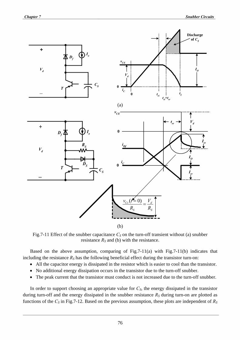
Chapter 7 Snubber Circuits
76
Io
+
_
Vd
T
Df
CS
iC
Vd
tri
IO
0
0
t2
vCE
Dischargeof CS
tri+trr (a)
Io
DS
+
_
Vd
T
RS
Df
CS
iC
vCE
Vdtrr
IO
Irr
IrriDf
0
0
( 0)Cs d
S S
v t VR R
==
(b)
Fig.7-11 Effect of the snubber capacitance CS on the turn-off transient without (a) snubber resistance RS and (b) with the resistance.
Based on the above assumption, comparing of Fig.7-11(a) with Fig.7-11(b) indicates that including the resistance RS has the following beneficial effect during the transistor turn-on:
• All the capacitor energy is dissipated in the resistor which is easier to cool than the transistor. • No additional energy dissipation occurs in the transistor due to the turn-off snubber. • The peak current that the transistor must conduct is not increased due to the turn-off snubber.
In order to support choosing an appropriate value for CS, the energy dissipated in the transistor during turn-off and the energy dissipated in the snubber resistance RS during turn-on are plotted as functions of the CS in Fig.7-12. Based on the previous assumption, these plots are independent of RS

Chapter 7 Snubber Circuits
77
and there is no additional energy dissipation in the transistor during turn-on due to the presence of the turn-off snubber. CS should be chosen based on the following issues:
• Keeping the turn-off switching locus within the reverse-bias safe operation area. • Reducing the transistor losses based on its cooling consideration. • Keeping the sum (shown as a dashed line in Fig.7-12) of the transistor turn-off energy
dissipation and snubber resistance energy dissipation low.
Fehler! Es ist nicht möglich, durch die Bearbeitung von Feldfunktionen Objekte zu erstellen.
Fig.7-12 Turn-off energy dissipation in the power switching device and the snubber resistance RS as a function of the snubber capacitance CS.
Having made initial selection of RS based on the Equation (7-32) and CS based on design trade-off, previously discussed, the designer must ensure that the capacitor has sufficient time to discharge down to low voltage, 0.1Vd, during the minimum on-state time of the transistor in order that the turn-off snubber be effective at the next turn-off interval [8].
During the on-state of the transistor, the capacitor discharge with a time constant C S SR Cτ = and the capacitor voltage given by:
/ C
S
tC dv V e τ−= (7-33)
therefore, discharging vCs down to 0.1Vd requires a time interval of 2.3τc thus:
on state 2.3 S St R C> (7-34)
As an example, assuming CS = CS1 (given in the Equation (7-28)) and RS is chosen using the Equation (7-32). Then the minimum on-state time of the transistor must be six times the transistor current fall time tfi (see Fig.7-15) [8].
7.7 Over-voltage snubber The stray inductions were neglected, when the turn-off snubber was described. Hence, there was
no over-voltage. The over-voltages at turn-off due to stray inductances, such as the one shown in Fig.7-11(a), can be minimized by means of the over-voltage snubber circuit shown in Fig.7-13. It is assumed here that it is possible to lump all the stray inductances together as indicated in Equation (7-25). The operation of over-voltage snubber can be described as the follows: initially the
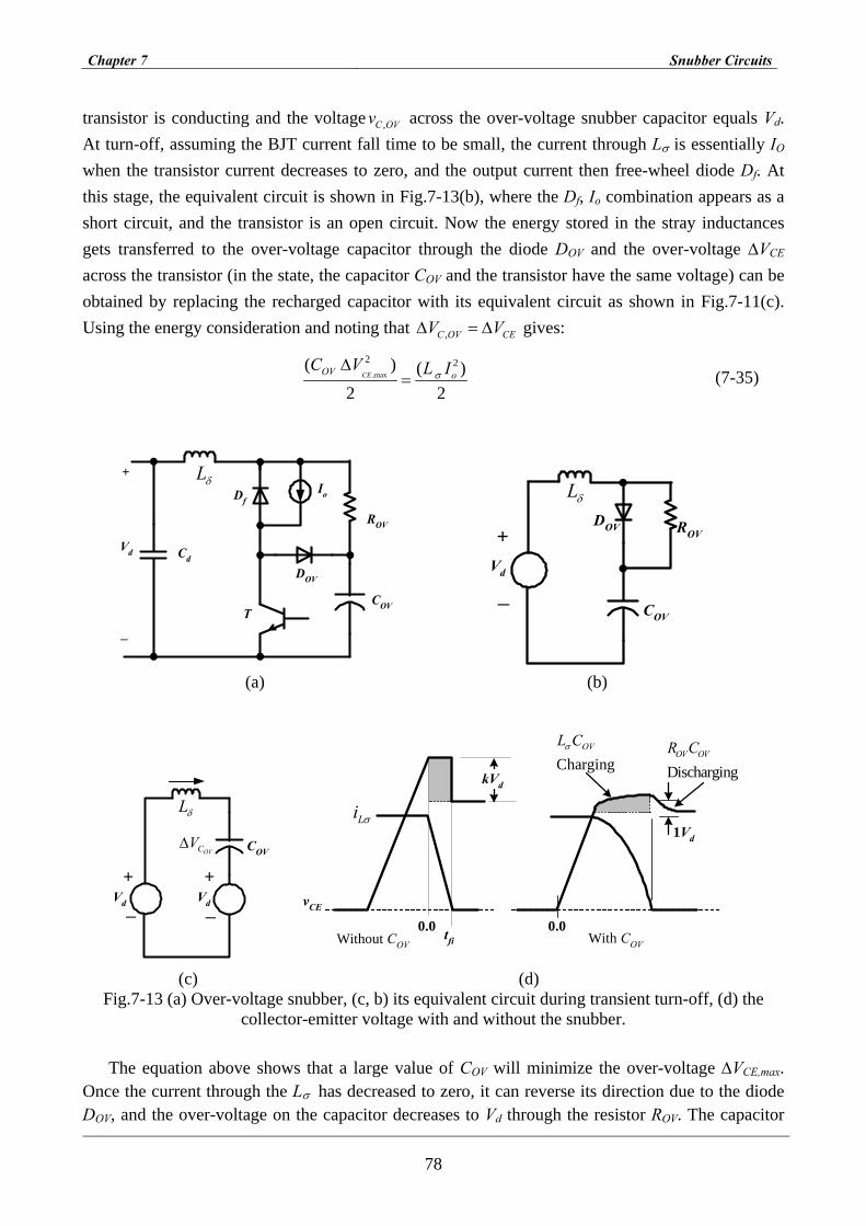
Chapter 7 Snubber Circuits
78
transistor is conducting and the voltage ,C OVv across the over-voltage snubber capacitor equals Vd. At turn-off, assuming the BJT current fall time to be small, the current through Lσ is essentially IO when the transistor current decreases to zero, and the output current then free-wheel diode Df. At this stage, the equivalent circuit is shown in Fig.7-13(b), where the Df, Io combination appears as a short circuit, and the transistor is an open circuit. Now the energy stored in the stray inductances gets transferred to the over-voltage capacitor through the diode DOV and the over-voltage ∆VCE across the transistor (in the state, the capacitor COV and the transistor have the same voltage) can be obtained by replacing the recharged capacitor with its equivalent circuit as shown in Fig.7-11(c). Using the energy consideration and noting that ,C OV CEV V∆ = ∆ gives:
,max
2 2( ) ( )2 2
CEOV oC V L Iσ
∆= (7-35)
Io
DOV
+
_
Vd
T
ROV
Df
COV
Cd
Lδ
Vd
DOV+
_
ROV
COV
Lδ
(a) (b)
Vd
+
_
COV
Lδ
Vd
+
_
OVCV∆
kVd
Li σ
vCE
0.0 tfiWithout COV
1Vd
0.0With COV
Charging OVL Cσ
Discharging OV OVR C
(c) (d)
Fig.7-13 (a) Over-voltage snubber, (c, b) its equivalent circuit during transient turn-off, (d) the collector-emitter voltage with and without the snubber.
The equation above shows that a large value of COV will minimize the over-voltage ∆VCE,max. Once the current through the Lσ has decreased to zero, it can reverse its direction due to the diode DOV, and the over-voltage on the capacitor decreases to Vd through the resistor ROV. The capacitor
Chapter 7 Snubber Circuits
79
discharge time constant OV OVR C should be small enough so that the capacitor voltage has decayed approximately to Vd prior to the next turn-off of the transistor. To support the estimation of the proper value of COV, the circuit waveforms with and without the over-voltage snubber are shown in Fig.7-13(d). The observed over-voltage of dk V without the over-voltage snubber is used to estimate Lσ as given by the following Equation:
/d o fikV L I tσ= (7-36)
If an over-voltage, for example, ,max 0.1CE dV V∆ = is acceptable, then using Equation (7-35) and substituting for Lσ from the Equation (7-36) yields:
,max
(100 ), ( 0.1 )o f i
OV CE dd
I tC V V
V= ∆ = (7-37)
In terms CS1which given by (7-28), COV from Equation (7-37) can be rewritten as:
1200OV SC k C= (7-38)
This shows that the substantially larger capacitance is needed for over-voltage protection compared to the values used in the turn-off snubber, which are on the order of CS1. It can be shown that even with a large value of COV the dissipated energy in ROV is of the same order as the energy dissipated in the resistor of the turn-off snubber. Both the turn-on and the over-voltage protection snubbers should be used simultaneously [8], [19], [20].
7.8 Turn-on snubber There is a large FBSOA (Forward Biased Safe Operating Area) of the most controlled switches
including BJT’s, MOSFET’s, GTO’s, and IGBT’s. So the turn on snubbers are only used to reduce turn-on switching losses at high switching frequencies and for limiting the maximum diode reverse recovery current. Turn-on snubber works by reducing the voltage across the switch (transistor) as the current builds up. A turn-on snubber can be in series with the transistor as shown in Fig.7-14(a) or in series with the freewheel diode as shown in Fig.7-14(b). In both circuits the turn-on and turn-off switching waveforms across the transistor and the freewheel diode are identical. The reduction in the voltage across the transistor during turn-on is due to the voltage drop across LS .This reduction is given by:
/ /CE S O ri S CE ri OV L I t L V t I∆ = ⇒ = ∆ (7-39)
where, tri is the current rise time as shown in Fig.7-14(c) for small values of LS. For such small values, di/dt is dictated only by the transistor and its base drive circuit and is assumed to be the same as without the turn-on snubber. Therefore, the diode peak reverse-recovery current is also the same as without the turn-on snubber. If it is important to reduce the diode peak reverse-recovery current, it can be achieved with a large value of LS as shown by the waveforms in Fig.7-14(d). Here the current rate of rise is di/dt = Vd/LS and the voltage across the transistor is almost zero during the current rise time. During the on-state of the transistor, LS conducts Io. When the transistor turns off, the energy stored in the snubber inductor 2( ) / 2S oL I will be dissipated in the snubber resistor RLS. The snubber time constant is /L S LSL Rτ = . When selecting RLS, the following two factors must be considered. First, during transistor turn-off, the turn-on snubber will generate an over-voltage across the transistor which is given by:

Chapter 7 Snubber Circuits
80
,max,max
CECE LS o LS
O
VV R I R
I∆
∆ = ⇒ = (7-40)
Io+
_
Vd
T
Df
LS
LSR
LSD
Io+
_
Vd
T
Df
LS
IoLSD
LSR
(a) (b)
vCE
Vd
iC
trrtrí
LS small
SdiLdt
vCE
iCLS Large
(c) (d)
Fig.7-14 Turn-on snubber circuit (a) in series with the power switching device or (b) in series with the free-wheel diode, (c) The power switching device voltage and current
waveforms for small value of Lσ and (d) for Large values of Lσ.
Second, during the off-state the inductor current must decay to a low value, for example 0.1IO, so that the snubber can be effective during the next turn-on. Therefore, the minimum interval for the off state of the BJT should be:
off state 2.3( / )S LSt L R> (7-41)
Thus a large inductance will result in lower turn-on voltage and lower turn-on losses. But it will cause over-voltage during turn-off, lengthen the minimum required off-state interval, and result in higher losses in the snubber. Therefore, LS and RS must be selected based on the above design trade-offs following a procedure similar to that described for the turn-off snubber. Since the turn-on snubber inductance must carry the load current, which makes this snubber expensive, it is rarely used alone.
However, if the turn-off snubbers are to be used in transistor bridge configurations, then turn-on snubbers must be used. It is possible to use all snubbers simultaneously or in any other combination.
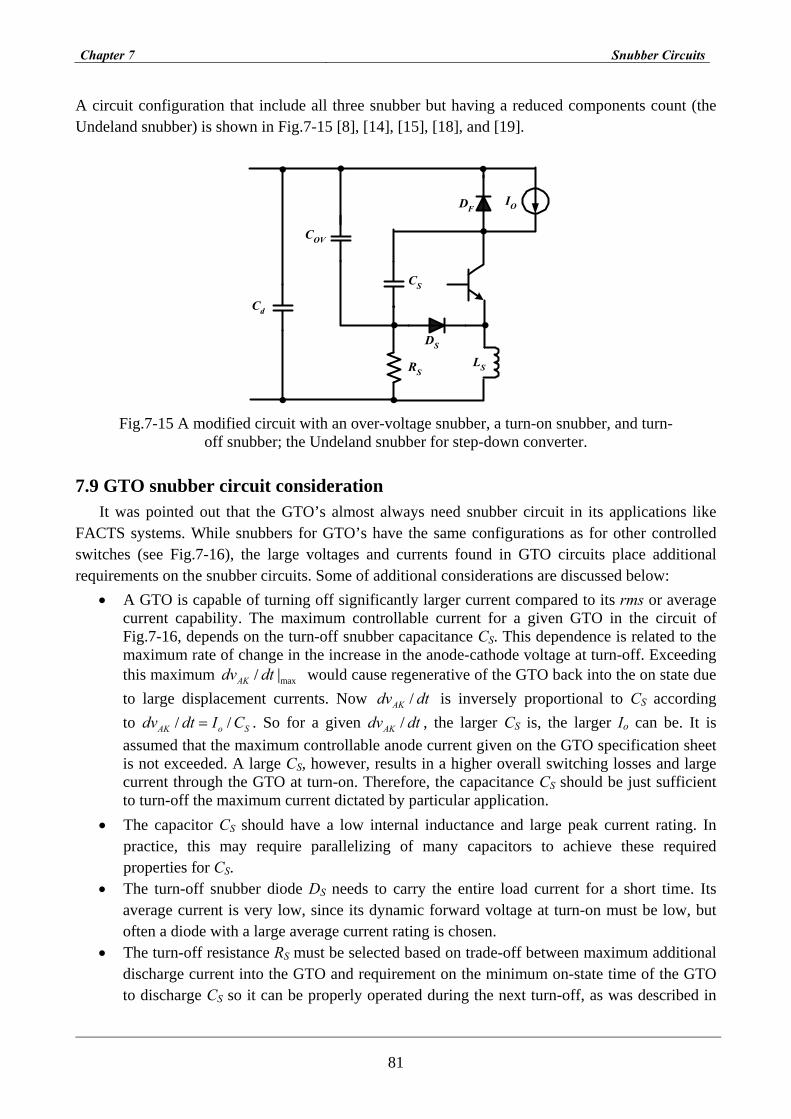
Chapter 7 Snubber Circuits
81
A circuit configuration that include all three snubber but having a reduced components count (the Undeland snubber) is shown in Fig.7-15 [8], [14], [15], [18], and [19].
RS
DS
DF
LS
COV
Cd
CS
IO
Fig.7-15 A modified circuit with an over-voltage snubber, a turn-on snubber, and turn-
off snubber; the Undeland snubber for step-down converter.
7.9 GTO snubber circuit consideration It was pointed out that the GTO’s almost always need snubber circuit in its applications like
FACTS systems. While snubbers for GTO’s have the same configurations as for other controlled switches (see Fig.7-16), the large voltages and currents found in GTO circuits place additional requirements on the snubber circuits. Some of additional considerations are discussed below:
• A GTO is capable of turning off significantly larger current compared to its rms or average current capability. The maximum controllable current for a given GTO in the circuit of Fig.7-16, depends on the turn-off snubber capacitance CS. This dependence is related to the maximum rate of change in the increase in the anode-cathode voltage at turn-off. Exceeding this maximum max/ |AKdv dt would cause regenerative of the GTO back into the on state due to large displacement currents. Now /AKdv dt is inversely proportional to CS according to / /AK o Sdv dt I C= . So for a given /AKdv dt , the larger CS is, the larger Io can be. It is assumed that the maximum controllable anode current given on the GTO specification sheet is not exceeded. A large CS, however, results in a higher overall switching losses and large current through the GTO at turn-on. Therefore, the capacitance CS should be just sufficient to turn-off the maximum current dictated by particular application.
• The capacitor CS should have a low internal inductance and large peak current rating. In practice, this may require parallelizing of many capacitors to achieve these required properties for CS.
• The turn-off snubber diode DS needs to carry the entire load current for a short time. Its average current is very low, since its dynamic forward voltage at turn-on must be low, but often a diode with a large average current rating is chosen.
• The turn-off resistance RS must be selected based on trade-off between maximum additional discharge current into the GTO and requirement on the minimum on-state time of the GTO to discharge CS so it can be properly operated during the next turn-off, as was described in

Chapter 7 Snubber Circuits
82
the turn-off snubber section. There is a considerable power loss in RS and therefore it may require mounting on heat sink.
RS
DS
Df
Cd
CS
IO
Vd
+
_
LON
RON
DON
GTO
Turn-onsnubber
Turn-offsnubber
Fig.7-16 Step-down converter circuit using a GTO as the switching device with turn-on and turn-off snubbers
It has already been described why the stray inductance in the turn-off snubber current loop should be as small as possible. To achieve this objective, the snubber components should be mounted as close to the GTO as possible. The design considerations for turn-on snubber for the GTO are similar to those described in the turn-on snubber section [8], [15], [19], and [20].
7.10 IGBT Snubber design
7.10.1 Over-voltage causes and their suppression Due to the high switching transistors of IGBTs at turn-off or during D1 (FWD Freewheel Diode)
reverse recovery, the current change rate (di/dt) is very high. Therefore, the circuit wiring inductance to the module can cause a high turn-of surge voltage ( / )V L di dt= .
For example, using IGBT’s waveform at turn-off will introduce the causes and the method of their suppression, as well as illustrate a concrete example of a circuit (using an IGBT and FWD together). Fig.7-17 shows the principle of a half-bridge, used as a test circuit, and the resulting voltage and current waveforms when switching IGBT1. The stray inductance LS, shown as a concentrated circuit element, represents all distributed inductances within the commutation loop.
When turning off the upper IGBT1, its current, whose magnitude is maintained by the inductive load, commutates into the diode D2 of the lower module for free-wheeling. IGBT1 takes over voltage up to the value of Ed and then, during the following fall time, the current is reduced through IGBT1 and at the same time is built up in diode D2 (see Fig.7-18). The current rate-of-rise di/dt,

Chapter 7 Snubber Circuits
83
dependent on current and voltage as well as temperature, is typically in the range of 3 6 /kA ms− ; values of up to 10 /kA ms can be reached under short circuit conditions. Due to the falling current a voltage drop of ( ( / ))S offL di dt− occurs across the stray inductance LS.
LS
IGBT1
IGBT2
VGE1 VCE1
Ed
IC1
ID2(=-IC2)
VD2(=-VCE2)
Load
D2
LO
RO
D1
Fig.7-17 Test chopper circuit.
(Ed: DC supply voltage, LS: main circuit wiring inductance, RO, LO: The load.)
If IGBT1 is turned on again, the load current commutates back from the branch of the diode D2 and is taken over again by IGBT1. Due to the rising current in this path a voltage drop of
( / )S onL di dt occurs over the stray inductance. This reduces the DC link voltage as long as diode D2 is still conducting. No voltage is taken over, until the peak of the reverse recovery current is exceeded. If this point is reached, it depends strongly on the recovery behavior of the diode, with which rate-of-rise the current goes through zero and with which rate-of-rise diode and anti-parallel IGBT must take over blocking voltage. High stray inductances and/or a snappy diode behavior may lead to considerable overvoltage spikes VCESP at this point. The VCESP: the turn-off surge voltage peak can be calculated as follows:
( ( / ))CESP d S CV E L di dt= + − (7-42)
where: /Cdi dt is the maximum collector current change rate at turn-off. If the voltage VCESP exceeds the IGBTs C-E (VCES) rating, then the module will be destroyed [21], [22], [23], [24], and [25].
7.10.2 Over-voltage suppression methods Several methods for suppressing turn-off surge voltage (as discussed before in this chapter). The
sources of the over voltages are listed below: • Control the surge voltage by adding a protection circuit (snubber circuit) to the IGBT. Use a
film capacitor in the snubber circuit. Place it as close as possible to the IGBT in order to bypass high frequency surge current.
• Adjust the IGBT driver circuits (-VGE) or RG in order to reduce the di/dt value. • Place the electrolytic capacitor as close as possible to the IGBT in order to reduce the
effective inductance of the wiring. Use a low inductance capacitor.

Chapter 7 Snubber Circuits
84
• To reduce the inductance of the main as well as snubber circuits wiring, and use thicker and short wires. It is also very effective to laminate the copper bars in wiring [21], [22], and [23].
IGBT1 turn-off0
0
0
VCEPS1
1IGBTV
1IGBTI
2DI
2IGBTV
IGBT1 turn-on
VCEPS2
VGE
Fig.7-18 IGBT Switching waveforms during the turn-off and turn-on processes
7.10.3 Type of IGBT snubber circuits and their features Snubber circuit is a supplementary circuit used in the converter circuit to reduce stress put on
the power semiconductor device. The ultimate goal of the snubber circuit is to improve the transient waveform. The snubber circuit suppresses over-current or over-voltage or improve dv/dt and di/dt to ease the transient waveform to reduce stress on the power semiconductor switching device. Snubber circuit can be divided into those connected to each IGBT and those connected in between the DC power supply and bus and ground. The first types of circuits include RC snubber circuits, charge and discharge RCD snubber circuits, and discharge-suppressing snubber circuits; while the second type includes C snubber circuit and RCD snubber circuits [21], [22], [23], and [24].
7.10.3.1 RC Snubber circuit
The RC snubber circuit, which is presented in Fig.7-19(a), is effective in turn-off surge voltage and suitable for chopper circuit. It is also effective for oscillation by parasitic reactance and dv/dt noise. However, when it is applied in large capacity IGBT, resistance for the snubber must be set to low to dissipation heat, so it has the disadvantage of worsening loading conditions at turn-on. Loss at the snubber itself is quite large, so it is not suitable for high frequency. In very large capacity IGBT circuit, it is better to use small snubber “RC snubber circuit” along with main snubber “discharge-suppressing RCD snubber circuit”. When used together, it helps parasitic oscillation control of the main snubber circuit loop. Main applications of this snubber circuit include arc welder and switching power supply [22].

Chapter 7 Snubber Circuits
85
7.10.3.2 Charge and discharge RCD Snubber circuit
This snubber suppresses over-voltage at turn-off to reduce switching losses at turn-off, and its effectiveness in surge voltage suppression is about average (see Fig.7-19(b)). The snubber capacitor is completely discharge at turn-on, and it is fully recharged at turn-off. Unlike the discharge-suppressing RCD snubber circuit below which acts as a clamp, this circuit reduces IGBT dv/dt during turn-off. As such, soft switching possible, and IGBT loss is reduced.
Since the structure of this circuit is snubber diode added to an RC snubber, snubber resistance can be increased, which alleviate the loop problem at turn-on. It is effective chopper applications, which use large current and low DC link voltage. Its advantage also includes no oscillation at its DC link voltage. The power loss due to the resistance is as follows:
2 21/ 2[( ) ( )]o S dP L I f C E f= + (7-43)
where L: the wiring inductance of the main circuit, IO: the collector current at IGBT turn-off, CS: the capacitor of the snubber circuit, Ed: DC supply voltage and f: the switching frequency.
However, losses from this circuit (mostly from snubber resistance) are significantly larger than the same in discharging suppressing RCD snubber circuit. As such, it is not suitable for high frequency switching applications. There are a lot of turn-off losses with bridge configuration. The disadvantages of this snubber circuit are relatively many parts and difficulties in selecting parts [21], [22].
7.10.3.3 Discharge-suppressing RCD snubber circuit The functions of this circuit as similar to those of voltage clamp snubber circuit (see Fig.7-
19(c)). Snubber capacitor is charged to the DC link voltage while the IGBT is in conduction, and VCE rises rapidly when IGBT is turn-off. Due to the stray inductance of the DC loop, VCE rapidly rises above the DC link voltage, so the snubber diode is forward biased conduction, and the snubber begins operation.
The energy stored in the stray inductance moves to snubber capacitor, which absorbs the energy without a rise in voltage. It has the advantages of small oscillation in DC link, and it is most practical in mid-to-large current applications. It is effect on turn-on voltage transient is neither large nor small. It is ideal for high frequency switching as its losses from the snubber circuit is small. The losses can be calculated with the following Equation:
21/ 2[( )oP L I f= (7-44)
where L: the wiring inductance of main circuit, IO: the collector current at IGBT turn-off and f: the switching frequency.
It is disadvantages are that it has many necessary parts and is less than effective on turn-off surge voltage. It is often used in inverters [21], [22].
7.10.3.4 C snubber circuit This is the simplest snubber circuit, so it has the advantages of suppressing over-current at
minimum cost (see Fig.7-19(d)). It is effective in mid-to-low current, low power applications, and as the power level increases, it becomes more likely for the circuit to oscillation as the snubber capacitor and the main circuit inductance from LC resonance circuit. It is often used in inverters [21], [22].

Chapter 7 Snubber Circuits
86
P
N
RC
N
P
RCD
RCD
N
P
(a) (b) (c)
P
N
C
N
RCD
(d) (e)
Fig.7-19 Schematic type of individual snubber circuits: (a) RC snubber circuit, (b) Charge discharge RCD snubber circuit, (c) Discharge suppressing RCD snubber circuit, (d) C snubber
circuit and (e) RCD snubber circuit.
7.10.3.5 RCD snubber circuit The RCD snubber circuit operates in the same manner as the C snubber circuit, but it is different
in that it operates during turn-off switching (see Fig.7-20(e)). It is a circuit that solved oscillation of the C snubber circuit by using the fast recovery diode. Energy that stored in DC loop inductance moves to the capacitor while the IGBT turns off. The snubber diode prevents oscillation from taking place. The charge from the capacitor is discharged through the snubber resistor. (RC time constant should be about 1/3 of the switching cycle. ( / 3 1/ 3T fτ = = ). This circuit reduces turn-off voltage transient directly. Switching waveform is significantly smoother and snubber loss is small. Effect on the turn-on voltage transient is fine, and it has the advantage of stable wave as the snubber diode blocks oscillation. It is practical in medium current range, but operation in large capacity IGBT, parasitic inductance increases to present problems in controlling over-voltage. In such large current applications, discharge-suppressing RCD snubber circuits are generally used. The functions of the discharge-suppressing RCD snubber circuit are similar to the functions of the RCD snubber circuits,

Chapter 7 Snubber Circuits
87
but the discharge-suppressing RCD snubber circuit has the advantage of small loop inductance as it is attached to the collector and the emitter of each device. This circuit cannot use in low inductance snubber capacitors designed to attached directly to the IGBT, and the blocking diode added to protection circuit can increase the total snubber inductance. Furthermore, if the recovery characteristics of the diode are not good, VCE over-shoot and dv/dt at either sides of the IGBT/diode, or the output voltage can oscillate. The Turn-off mechanism is nearly the same as that of the discharge-suppressing RCD snubber circuit [21], [22].
7.10.4 Discharge-suppressing RCD snubber circuit design The discharge suppressing RCD snubber can be considered the most suitable snubber circuit for
IGBTs. Basic design methods for this type of circuit will be explained in the following points.
7.10.4.1 A Study of applicability Fig.7-20 shows the turn-off locus waveform of an IGBT in a discharge-suppressing RCD
snubber circuit. Fig.7-21 shows the IGBT current and voltage waveforms at turn-off. The discharge-suppressing RCD snubber circuit is activated when the IGBT C-E voltage starts to exceeds the DC supply voltage [20]. The dotted line diagram in Fig.7-20 shows the ideal operating locus of an IGBT. In an actual application, the wiring inductance of the snubber circuit or a transient forward voltage drop in the snubber diode can cause a spike voltage at IGBT turn-off.
This spike voltage causes the sharp-concerned locus indicated by the solid line in Fig.7-21. The discharge-suppressing RCD snubber circuits’ applicability is decided by whether or not the IGBTs operating locus is within the RBSOA (Reverse Biased Safe Operating Area) at turn-off. The spike voltage at IGBT turn-off is calculated as follows:
( ( / ))CESP d FM S CV E V L di dt= + + − (7-45)
where: Ed: DC supply voltage, LS: the snubber circuit wiring inductance, VFM: the transient forward voltage drop and /Cdi dt maximum collector current change rate at IGBT turn-off. The reference values for the transient forward voltage drop in snubber depending on diode are: 600 V class: 20 to 30V, and 1200V class: 40 to 60V [18], [21], [22].
IC
VCEVCES
VCEP
VCESP
RBSOA
(Pulse)
iC
I0VCESP VCES
VCE
Fig.7-20 Turn-off locus waveform of IGBT. Fig.7-21 Voltage and current waveforms at turn-off. IGBT.

Chapter 7 Snubber Circuits
88
7.10.4.2 Calculating the capacitance of the snubber circuit capacitor The necessary capacitance of a snubber capacitor CS is calculated as follows:
2 2/(( ) )S o CEP dC L I V E= − (7-46)
where: L: the main circuit wiring inductance, VCEP: the snubber capacitor peak voltage, Io: the collector current at IGBT turn-off and Ed: DC supply voltage. The VCEP must be limited to less than or equal to the IGBT C-E withstand voltage [21].
7.10.4.3 Calculating snubber resistor The function required of snubber resistance RS is to discharge the electric charge accumulated in
the snubber capacitor before the next IGBT turn-off. To discharge 98% of the accumulated energy by the next IGBT turn-off, the snubber resistance must be satisfying the following inequality:
1/(2.3 )S SR C f≤ (7-47)
where: f is the switching frequency. If the snubber resistance is set too low, the snubber circuit current will oscillate and the peak collector current at the IGBT turn-off will increase. Therefore, the snubber resistance is set in a range below the value calculated in the Equation (5-46). Irrespective of the resistance, the power dissipation loss P (RS) is calculated as follows [21]:
2( ) ( ) / 2S oP R L I f= (7-48)
7.10.4.4 Snubber diode selection A transient forward voltage drop in the snubber diode is one factor that can cause a spike
voltage at IGBT turn-off. If the reverse recovery time of the snubber diode is too long, then the power dissipation loss will also be much greater during high frequency switching. If the snubber diodes reverse recovery is too hard, then the IGBT C-E voltage will drastically oscillate. The selecting of the snubber diode that has a low transient forward voltage, short reverse recovery time and a soft recovery [18], [20], [21].
7.10.4.5 Snubber circuit wiring precautions The snubber circuits wiring inductance is one of the main causes of spike voltage, therefore it is
important to design the circuit with the lowest possible inductance [21].
Chapter 8 Simulation results of three-level VSC snubber circuits
89
8 Simulation results of three-level VSC snubber circuits
8.1 Introduction In this chapter, the three-level Voltage-Sourced Converter with the common snubber and the
new suggested snubber circuit will be discussed. Depending on the snubber circuit strategy, which was studied in the chapter7, recommended and new snubber circuit design will be presented which are suitable for the three-level Voltage-Sourced Converter. The Study will be supported by computer simulations and practical tests.
8.2 Common snubber circuit for three level inverters
In the recent years, modern power semiconductor switching devices like GTO’s (Gate Turn-off Thyristors), IGBT’s (Insulated Gate Bipolar Transistors), and IGCT’s (Integrated Gate Commutated Thyristors) (discussed in Chapter3), which have the ability to be turned-off via a gate-control, have attracted more and more attention to be used in very large voltage-sourced inverters, FACTS (Flexible AC Transmission Systems) devices or modern HVDC systems. These systems with a rated power of 300MVA and above make it possible to increase the power transmission capacity of the existing lines or to improve the stability of the today and future power systems. The inverters require specialized high power gate controlled valves due to their high MVA rated power. At present, the GTO and the IGCT is still the most practical power switching device available for use in these circuits. GTO’s with the maximum voltage and maximum current of are now commercially available. Several of these devices must be connected in series to constitute a single valve for the above applications. In general, very specific protection systems (snubber circuits as discussed in Chapter7) should be used to reduce and prevent the stresses, which result from the switching (on-off and off-on) processes.
The main goal is to keep the power semiconductor device within the SOA (Safe Operation Area) defined by the manufacturer [26], [27], [31]. Basically, the power semiconductor switching devices, which can be used in the high-power systems described above, require a series snubber circuit (inductance) that limits the current-time-divertive di/dt at turn-on, and a parallel snubber circuit (capacitance) that limits the voltage-time-divertive dv/dt during the turn-off. The two snubber circuits cannot be considered as disjoint circuits but they must be seen as a coupled auxiliary circuit design (see Fig.8-1) [28], [29], [30]. In fact, snubber circuits can be divided in three types: Unpolarized series RC snubbers, polarized RCD snubbers and polarized RLD (which were discussed in Chapter7). In details, a single-phase schematic of a three level converter is shown in Fig.8-1. The snubber circuit for the shown partial network of a three level converter uses separate elements and integrated into separate sub-circuit [31], [32], [33], [34], and [35].
8.3 Double snubber circuit for three level inverters Here a new snubber circuit configuration will be subjected; the proposed double snubber
circuit uses an additional RC snubber to optimize the damping of the turn-off snubber configuration. Therefore, the over voltage can be reduced effectively by an optimization of the passive components and its parameters in the new design. The double snubber makes it possible to reduce the high peak power of the losses during switching off the semiconductor devices associated with

Chapter 8 Simulation results of three-level VSC snubber circuits
90
the simultaneous maximum of the voltage and the current. In this way, the proposed circuit allows a minimization of both the over voltage and the switching losses [31], [34], and [36]. The common snubber circuit shown in Fig.8-1 composes of two standard turn-on RLD snubbers (RON1, LON1 DON1,
RON2, LON2, and DON2), but the double snubber configuration consisting of the same snubber circuit configuration and an extra RC network connected in parallel to the RCD as shown in Fig.8-2.
LON1
RS1DS1
CS1
Vd
Rd
RON1
DC1
DC2
C2
C1
DON1
The Load
GTO1Df1
RS2DS2
CS2
GTO2Df2
RS3DS3
CS3
GTO3Df3
RS4DS4
CS4
GTO4Df4
LON2
RON2
Ed
Ed
DON2
Turn-off snubberTurn-on snubber
Fig.8-1 Single phase of a three level converter (common snubber circuit).
The RC snubber has several advantages: It allows reducing losses in the circuit and the switching device. Additionally, the peak voltage is limited. During the charging of CS which is limiting the dv/dt during the off process, the effective value of RS is essentially close to zero. This is not the optimum value for RS. In most cases, transient phenomena will cause an essentially higher over voltage or at least more than necessary [8], [37], [38], [39], [40], [41], [42], [43], and [44]. Table 8.1 shows the total number of protection elements RSµ, CSµ, Ronµ, Lonµ and snubber diodes Dµ in the common- and proposed double snubber circuit configurations. However, the common snubber circuit uses fewer elements than the proposed double snubber circuit, where the proposed double snubber circuit design needs more passive components. Therefore, the implementation of the

Chapter 8 Simulation results of three-level VSC snubber circuits
91
double snubber circuit is favorable, especially, in cases when the optimization of losses and/or over voltages is of highest interest [28], [30], [42], [43], [44], and [45].
Components Capacitors Diodes Inductors Resistors
Common Snubber Circuit configuration 4 6 2 6
Double Snubber Circuit configuration 8 6 2 10
Table 8.1 the total number of snubber elements for the different snubber designs. [28], [32].
LON1
RS1DS1
CS1
Vd
Rd
RON1
DC1
DC2
C2
C1
DON1
The Load
GTO1Df1
RS2DS2
CS2
GTO2Df2
RS3DS3
CS3
GTO3Df3
RS4DS4
CS4
GTO4Df4
LON2
RON2
Ed
Ed
DON2
Double snubber citcuit
RP1
CP1
RP2
CP2
RP3
CP3
RP4
CP4
Fig.8-2 Proposed double snubber circuit configuration in a three level inverter system.
8.4 An optimized snubber design for three level inverters The other proposed design is an optimized snubber design which consists of a centre-tapped
inductor (LON1, LON2), a damping resistor (RON), four diodes (DON1, DON2, DS1, DS2), four capacitors (CS1, CS2, CS3, CS4), and two resistors (RS1, RS2) for each arm of the three-phase inverter system as shown in Fig.8-3 [8], [28], [36], [47], and [48]. Table 8.2 compares between the number of components for the common snubber circuit (RLD/RCD) and the new optimized snubber design. The new optimized design includes only three resistors while the common snubber needs six resistors [8], [36].
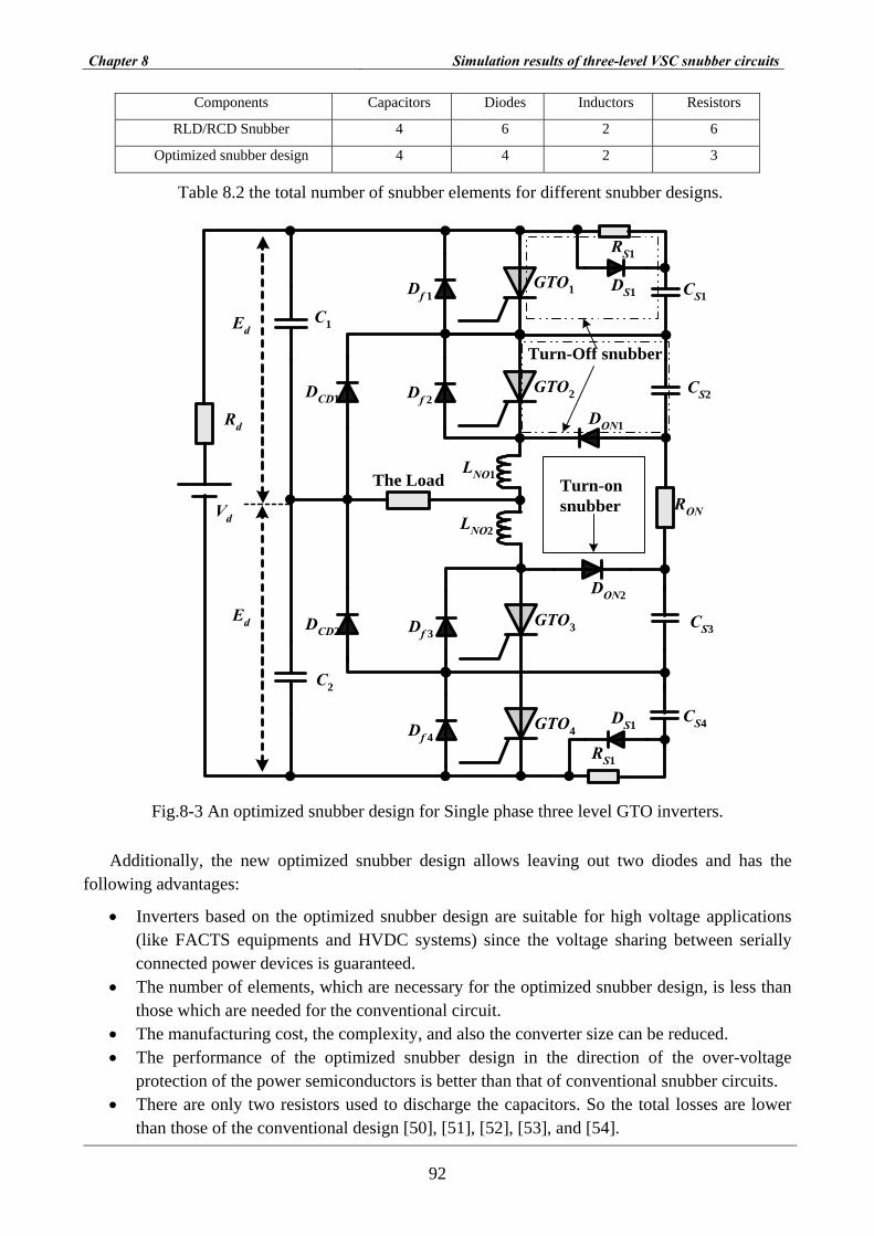
Chapter 8 Simulation results of three-level VSC snubber circuits
92
Components Capacitors Diodes Inductors Resistors
RLD/RCD Snubber 4 6 2 6
Optimized snubber design 4 4 2 3
Table 8.2 the total number of snubber elements for different snubber designs.
CS1
RON LNO2
DON2
DON1
CS2
CS3
CS4
DS1
RS1
RS1
C1
C2
Ed
DCD2
DCD1
The Load
Rd
Vd
GTO1 Df 1
GTO2 Df 2
GTO3 Df 3
GTO4 Df 4
LNO1
Ed
DS1
Turn-onsnubber
Turn-Off snubber
Fig.8-3 An optimized snubber design for Single phase three level GTO inverters.
Additionally, the new optimized snubber design allows leaving out two diodes and has the following advantages:
• Inverters based on the optimized snubber design are suitable for high voltage applications (like FACTS equipments and HVDC systems) since the voltage sharing between serially connected power devices is guaranteed.
• The number of elements, which are necessary for the optimized snubber design, is less than those which are needed for the conventional circuit.
• The manufacturing cost, the complexity, and also the converter size can be reduced. • The performance of the optimized snubber design in the direction of the over-voltage
protection of the power semiconductors is better than that of conventional snubber circuits. • There are only two resistors used to discharge the capacitors. So the total losses are lower
than those of the conventional design [50], [51], [52], [53], and [54].

Chapter 8 Simulation results of three-level VSC snubber circuits
93
Because of the fewer elements in the snubber circuit, the theoretic reliability will be higher. Therefore, the implementation of the optimized snubber design is favorable especially in cases of the optimization of the losses and/or over-voltage is of highest inertest. To analyze the physical background of the protection performance, some of the basics of different switching operations have to be discussed. Therefore, the possible switching states of a single phase of a three level inverter system are listed in Table 8.3. Due to the symmetry, it is sufficient to consider only a complete cycle of communication process: 0 1 0 1S S S S−→ → → assuming that the load current is flowing.
Switching states S1 S0 S-1
GTO1 ON OFF OFF GTO2 ON ON OFF GTO3 OFF ON ON GTO4 OFF OFF ON
Table 8.3 the three Switching States.
There is an important assumption which simplifies the analysis of the snubber design: The Thyristor current changes linearly in time with a constant di/dt (the load current is constant, In most applications the time constant of the load (some milliseconds) is much larger than the switching time (in the sub-microseconds), so the load current IL remains almost constant during the switching period), which is only dictated by the GTO-Thyristor current (or other devices) and its base driver’s circuit. Therefore, di/dt, which may be different for the turn-on and the turn-off processes, is assumed not to be affected by adding the snubber circuits. Also, it is assumed that the time constant of the load (milliseconds) is much larger than the switching time (in the microsecond range). So the load current IL remains almost constant during the switching period. Based on these premises the relevant transition or commutation phases will be closer analyzed later in this Chapter [50].
Commutation from S0 to S1: The current transition in this phase is defined by the turning-off of GTO3. After a defined dead
time, GTO1 is turned on. During that period, the load current is flowing through the clamping diode DC1 and GTO2. The snubber capacitors CS1 and CS4 are charged up to Ed and CS2, CS3 are totally discharged (see Fig.8-4(a)). Phase 1: The semiconductor switching device GTO1 starts turning on, so the current flowing through it begins to increase and the current through the clamping diode DC1 starts to decrease and the capacitor CS1 begins to discharge in the loop which is formed through GTO1 and RS as shown in Fig.8-4(b). Phase 2: In this step, the current through GTO1 continues to increase during the current rise time. As soon as the clamping diode DC1 ceases to conduct, the load terminal voltage goes up charging CS3. At the end of this step the capacitor CS1 is completely discharged and the energy which is stored in LON2 will be dissipated through the loop DON2, RON, DON1, LON1 (see Fig.8-4(c)).
Commutation from S1 to S0:
During this phase GTO1 is turned off and GTO3 is turned on after the necessary dead time. The initial condition for this period is the final state of the previous commutation. During the turn-off period of GTO1 the load current is absorbed by CS1 (see Fig.8-5(a)) [50].

Chapter 8 Simulation results of three-level VSC snubber circuits
94
CS1
RON LNO2
DON2
DON1CS2
CS3
CS4
DS1
DS2
RS2
C1
C2
Ed
DCD2
DCD1
Rd
Vd TheLoad
Df 1
Df 2
Df 3
Df 4
LNO1
Ed
RS1
GTO2(ON)
GTO3(ON)
GTO4(OFF)
GTO1(OFF)
CS1
RON LNO2
DON2
DON1
CS2
CS4
DS1
DS2
RS2
C1
C2
Ed
DCD2
DCD1
Rd
Vd TheLoad
Df 1
Df 2
Df 3
Df 4
LNO1
Ed
GTO2(ON)
GTO1(ON)
GTO3(OFF)
CS3
GTO4(OFF)
(a) (b)
CS1
RON LNO2
DON2
DON1
CS2
CS3
CS4
DS1
DS2
RS2
C1
C2
Ed
DCD2
DCD1
Rd
Vd TheLoad
Df 1
Df 2
Df 3
Df 4
LNO1
Ed
RS1
GTO2(ON)
GTO1(ON)
GTO4(OFF)
GTO3(OFF)
(c)
Fig.8-4 Commutation path of the transition form S0 to S1: (a) initial state, (b) phase 1 and (c) phase-2
Phase 1: In Phase 1, iGTO1 decreases linearly from ILOAD to zero during the current fall time period and the load current starts to charge CS1 through the turn-off diode DS1.This step ends when iGTO1 reduces to zero see (Fig.8-5(b)). Phase 2: In Phase 2 the CS1 is completely charged. Finally the complete load current flows through the clamping diode DC1. After that, GTO3 begins to turn-on after a suitable dead time. In this case the commutation process is completed (see Fig.8-5(c)) [28], [37].

Chapter 8 Simulation results of three-level VSC snubber circuits
95
CS1
RON LNO2
DON2
DON1
CS2
CS3
CS4
DS1
DS2
RS2
C1
C2
Ed
DCD2
DCD1
Rd
Vd TheLoad
Df 1
Df 2
Df 3
Df 4
LNO1
Ed
RS1
GTO2(ON)
GTO1(ON)
GTO3(OFF)
GTO4(OFF)
CS1
RON LNO2
DON2
DON1
CS2
CS3
CS4
DS1
DS2
RS2
C1
C2
Ed
DCD2
DCD1
Rd
Vd TheLoad
Df 1
Df 2
Df 3
Df 4
LNO1
Ed
RS1
GTO2(ON)
GTO1(OFF)
GTO3(ON)
GTO4(OFF)
(a) (b)
CS1
RON LNO2
DON2
DON1
CS2
CS3
CS4
DS1
DS2
RS2
C1
C2
Ed
DCD2
DCD1
Rd
Vd TheLoad
Df 1
Df 2
Df 3
Df 4
LNO1
Ed
RS1
GTO1(OFF)
GTO2(ON)
GTO3(OFF)
GTO4(OFF)
(c) Fig.8-5. Commutation path of the transition form S1 to S0: (a) initial state, (b) phase 1 and (c)
phase-2.
Commutation from S0 to S−1: During this phase GTO2 is turned off and GTO4 is turned on after the corresponding dead time.
The initial conditions are the following: CS1 and CS4 are completely charged up to Ed; CS2 and CS3 are completely discharged and the load current flows through the free wheeling diodes Df3 and Df4 as presented in Fig.8-6(a).

Chapter 8 Simulation results of three-level VSC snubber circuits
96
Phase 1: When GTO2 is turned off the load current will be absorbed by CS2 charging it. During GTO2 is turned off, the voltage drop across GTO1 remains Ed, while the voltage drop across GTO2 is increasing. iGTO2 decreases linearly from ILOAD to zero during the current fall time. This step ends when iGTO2 reached zero (see Fig.8-6(b))[28], [31], [36], and [50].
Phase 2: The voltage over GTO2 continues to rise in this which ends when 2SCV reaches Ed. The
energy which is stored in LON1 will be dissipated through the loop DON2, RON, DON1, LON1 (see Fig.8-6(c)) [28], [31], [36], and [50].
Note: During the discharging process of the capacitor CS2, the discharging current will flow through the following elements: GTO2, LON1, LON2, DON2, RON, CS2 (see Fig.8-6c).
CS1
RON LNO2
DON2
DON1
CS2
CS3
CS4
DS1
DS2
RS2
C1
C2
Ed
DCD2
DCD1
Rd
Vd TheLoad
Df 1
Df 2
Df 3
Df 4
LNO1
Ed
RS1
GTO4(OFF)
GTO3(OFF)
GTO2(OFF)
GTO1(OFF)
CS1
RON LNO2
DON2
DON1
CS2
CS3
CS4
DS1
DS2
RS2
C1
C2
Ed
DCD2
DCD1
Rd
Vd TheLoad
Df 1
Df 2
Df 3
Df 4
LNO1
Ed
RS1
GTO1(OFF)
GTO2(OFF)
GTO3(OFF)
GTO4(OFF)
(a) (b)
GTO1(OFF)
GTO3(ON)
GTO4(ON)
GTO2(OFF)
CS1
RON LNO2
DON2
DON1
CS2
CS3
CS4
DS1
DS2
RS2
C1
C2
Ed
DCD2
DCD1
Rd
Vd TheLoad
Df 1
Df 2
Df 3
Df 4
LNO1
Ed
RS1
CS2discharging-path
(c)
Fig.8-6 Commutation path of the transition form S0 to S-1: (a) initial state, (b) phase 1 and (c) phase-2.

Chapter 8 Simulation results of three-level VSC snubber circuits
97
8.4.1 Performance of the optimized snubber design The main advantage of the optimized snubber design is that the three snubber circuits (turn-on,
turn-off, and over-voltage) are used in combination and that the number of the required elements is less than those which are necessary for the common snubber circuit. The operation of the power semiconductor switching devices still remains in the SOA. Additionally the converter size, its cost, and the losses can be reduced. Fig.8-7 shows a three level inverter with the corresponding optimized snubber design.
• The turn-off snubber circuit protects the power switching semiconductor device from the over-voltage, which appears during the turn-off process, because of the high current change rate di/dt. Therefore, the circuit wiring inductance can cause a high turn-off surge voltage. The charging process takes place as in the common snubber circuit, through the turn-off diode. The discharging process occurs through the power semiconductor switching device, the turn-on resistor, and the mid-point inductance for the second and third GTO. The charging and discharging of GTO1 and GTO4 is realized in the ‘normal’ way by DS1/DS2 and RS1/RS2, respectively.
• The turn-on snubber’s circuits limits the di/dt during turning on and reducing the voltage across the power semiconductor switching device due to the voltage drop across the inductance when the current builds up. During the on-state of the power semiconductor switching device, the load current flows through the turn-on inductance. When the power semiconductor switching device is turned off, the stored energy in the snubber inductance will be dissipated in the resistor RON. When GTO1 and GTO2 are switched on and off, the inductor LON2 will decay the current to low value. So the snubber circuit will be effective in the next turn-on, and vice versa, LON1 will do the same during GTO3 and GTO4 switching.
• The over-voltage snubber circuit minimizes the over-voltage which is caused by the stray- and turn-on inductance across the power semiconductor switching device to safe levels. The energy stored in LON1 gets transferred to the turn-off capacitor CS2 through the diode DON1. So, there is no over-voltage across the power semiconductor switching device because it will be limited to Ed through the resistor RON. This snubber circuits consist of the following elements: CSµ, RON, DONµ, and DSµ [50], [38], [39], and [40].
8.5 Dual-use snubber circuit for three-level inverter The suggested snubber circuit “the dual-use snubber circuit,” is the modified design of the
optimized snubber design. The modification in is in the position of the turn-off snubber resistor RSµ. The turn-off resistor RSµ will be replaced to have a new position as presented in Fig.8-8. The new location of the resistor RSµ will give the snubber circuit design the same advantages of the optimized snubber circuit and an extra advantage. While the resistor RSµ in this case is much more useful during the turn-off processes and has two functions [8], [28], [31], [36], and [50]:
• The first function is during the discharge process of CS1. The capacitor energy will be dissipated in it and the discharge current will be limited.
• The second function is during the charging process of CS2, The resistor has a damping effect of the over-voltage across the power switching device while charging process of CS2. Therefore, the over-voltage will be reduced, especially in the beginning of turn-off process [55], [56], and [57].

Chapter 8 Simulation results of three-level VSC snubber circuits
98
CS1
RON LNO2
DON2
DON1
CS2
CS3
CS4
DS1
DS1
RS1
C1
C2
Ed
DCD2
DCD1
The Load
Rd
Vd
GTO1 Df 1
GTO2 Df 2
GTO3 Df 3
GTO4 Df 4
LNO1
Ed
RS1
Fig.8-7 One phase of a three level inverter with the new dual-use snubber circuit design.
8.6 Dual-inductive snubber circuit for three-level Inverter This is the developed module of the dual-use snubber circuit to update the dual-use snubber circuit design in order to get more new features and optimized performance of the snubber circuit. It comprises the three snubber circuit (turn-on, turn-off and over-voltage) and has a parallel inductor with the turn-on resistor (see Fig.8-8). The performance of the dual-inductive snubber circuit is better than the performance of common snubber circuits, especially the limitation of the current, suppressing the over-voltage and minimization of the losses. The dual-inductive snubber circuit has additionally more advantages than the dual-use snubber design which are mentioned in the following:
• The dual-inductive snubber design suppresses the over-voltage protection of the power semiconductors much more than that of conventional snubber circuits, because of the new arrangement of the snubber circuit elements.
• The parallel inductor will decay the current during the turn-on process to a lower value. So the turn-on snubber circuit is more effective.
• The resulting voltage over RON will drop nearly to zero when the turn-on process is over because of the parallel inductor LONP. Therefore the losses in RON during the on-states drop fundamentally when the transient processes are decayed.
• The parallel inductor can be a primary winding of transformer which can be effective as a power recovery system.

Chapter 8 Simulation results of three-level VSC snubber circuits
99
• The theoretical reliability is higher because of the fewer elements in the snubber circuit [36], [50], and [57].
CS1
RON
LNO2
DON2
DON1
CS2
CS3
CS4
DS1
DS1
RS1
C1
C2
Ed
DCD2
DCD1
Rd
Vd The Load
GTO1 Df 1
GTO2 Df 2
GTO3 Df 3
GTO4 Df 4
LNO1
Ed
RS1
LONP
Fig.8-8 One phase of a three-level inverter with the new dual-inductive snubber circuit.
8.7 Simulation and discussion of the results The simulation will be based on a detailed Matlab(R)/SimulinkTM model. The analyzed model
comprises a single phase of a MV three level inverter. The load and source data are presented in the following Table 8.4. The internal parameters of the GTO and its common snubber circuit (which are RS, CS) were taken from the data sheet of the used GTO semiconductor devices. Table 8.4 shows the parameters of the used GTO and the load information.
GTO parameters
Forward-voltage
Vf (V)
Internal resistor
RON (Ω)
Internal reactance
LON (µΗ)
Current fall time
tfi (µs)
Snubber resistor
RS (Ω)
Snubber capacitor
CS (µF)
1 0.001 1 5 5 1
Load and source data Load voltage Ed (V) Load current IL (A) Power factor Pf
6000 4600 0.8
Table 8.4 the parameters of the used GTO and the load information.

Chapter 8 Simulation results of three-level VSC snubber circuits
100
8.7.1 Description of the PWM in Matlab®/SimulinkTM
Power semiconductor devices are used as mentioned before to control the voltage and the current of converter systems, because it has lower energy losses compared with other continuous controller like resistor. The pulsed control system will be used to drive the power semiconductor devices for achieving high efficiency The pulse width modulation (PWM) is the most widely used type of control system for the power semiconductor devices when it needs to control the output of the converter systems. For achieving smooth control of the voltage or current the switching frequency (commutation frequency) should be relative high (kHz).
The circuitry of the PWM will be built in Matlab®/SimulinkTM tools. The circuitry consists of the block components, which can give the needed PWM (e.g. 2-3kHz), those components contain the sine wave (50Hz) which is the voltage reference, the pulse generator which give pulse scheme which will be generate the saw wave (tri-angle pulse scheme) at the required switching frequency (see Fig.8-9), and the comparison box which contains the comparison elements like great- or less- than, and logic elements And/Or, the main aim of this box is to compare between the sine wave and the saw wave, as presented in Fig.8-9 and Fig.8-10. The output of the comparison will be true (1) if the sine wave is bigger than the saw wave, this means that the IGBT will switch on during this time, or false (0) when the saw wave is bigger than the sine wave, as shown in Fig.8-11. Fig.8-12 shows the pulse scheme of the Matlab®/SimulinkTM simulation which will drive the IGBT at the frequency of e.g.3 kHz. This pulse scheme will be used as reference in other programming tools (will be discussed in Chapter9). With the programming tools, the pulse scheme, which will drive the gates of IGBT converter, is the output of the microcontroller chip which will be the driver system.
Fig.8-9 The main flow chart of the PWM in Matlab®/SimulinkTM.

Chapter 8 Simulation results of three-level VSC snubber circuits
101
Fig.8-10 The internal part of the PWM in Matlab®/SimulinkTM.
0,000 0,005 0,010 0,015 0,020
-1,0
-0,5
0,0
0,5
1,0
Sin
e, S
aw [p
.u]
t [s]
Sine wave Saw wave 1 Saw wave 2
Fig.8-11 The comparison functions of the PWM in Matlab®/SimulinkTM.

Chapter 8 Simulation results of three-level VSC snubber circuits
102
0,000 0,005 0,010 0,015 0,020 0,025 0,0300,00,20,40,60,81,0
0,000 0,005 0,010 0,015 0,020 0,025 0,0300,00,20,40,60,81,0
0,000 0,005 0,010 0,015 0,020 0,025 0,0300,00,20,40,60,81,0
0,000 0,005 0,010 0,015 0,020 0,025 0,0300,00,20,40,60,81,0
t[s]
t[s]
IGTO4
IGTO3
IGTO2
t[s]
t[s]
IGTO1
Fig.8-12 the output of the PWM in Matlab®/SimulinkTM.
8.7.2 Comparison of the proposed double snubber configuration and the common snubber circuit
In this simulation, the proposed double snubber configuration will be compared with the common snubber circuit. The parameters of the common snubber circuit are constant (standard values). The values of the proposed double snubber configuration were chosen exactly in the same way, but the value of CS and RS were reduced to other values as in Table 8.5. While this reduction improves the performance of the double snubber circuit, the results for the common snubber configuration remain nearly the same. Additionally the values of the parallel parameter will be set to different values to indicate to its effect. Table 8.5 gives the values of snubber circuits in all simulation cases.
Snubber circuit data Double snubber configuration Common snubber
CS (µF) 1 0.5 1
RS (Ω) 5 2.5 5
CP (µF) 0.05 0.01 -
RP (Ω) 5 1 -
Table 8.5 Snubber circuits (common and double configuration) information.
The simulation’s results for the first value ( 0.05 FPC µ= ) are presented in Figs 8-13 to 8-18. Figs 8-13 and 8-14 show the current and the voltage on GTO1 and GTO2. The overvoltage is limited in a better way by the double snubber configuration and the current peaks are much smaller as shown in Fig.8-14.

Chapter 8 Simulation results of three-level VSC snubber circuits
103
0,0050 0,0075 0,0100 0,0125 0,0150
6000
0,000 0,005 0,010 0,015 0,0205000
6000
7000
uGTO2-C
uGTO2-D
uG
TO2 [V
]
t [s]
uG
TO1 [V
]
t [s]
uGTO1-C
uGTO1-D
Fig.8-13 The voltages on GTO1 and GTO2 in the common and the double snubber configuration (CP=0.05µF).
0,000 0,005 0,010 0,015 0,0200
1000
2000
3000
4000
5000
60000,000 0,005 0,010 0,015 0,020
0
1000
2000
3000
4000
5000
6000
iGTO2-C
iGTO2-D
i GTO
2 [A]
t [s]
t [s]
i GTO
1 [A] iGTO1-C
iGTO1-D
Fig.8-14 The currents in GTO1 and GTO2 in the common and the double snubber configuration (CP=0.05µF).
The Figs 8-15, 8-16 and 8-17 show the current and the voltage in the freewheel diode and in the turn-off diode. It can easily be seen that the current and the voltages resulting from the new proposed protection circuits are more favorable than those simulated for the conventional circuit. In Fig.8-18 the total losses in the conventional circuit in the proposed double snubber design are compared based on energy function over two cycles of the fundamental frequency. As indicated, the energy lost in the entire new snubber circuit is much lower than in the standard snubber design. Also, the losses in the GTO itself are less for the new design but do not differ too much.
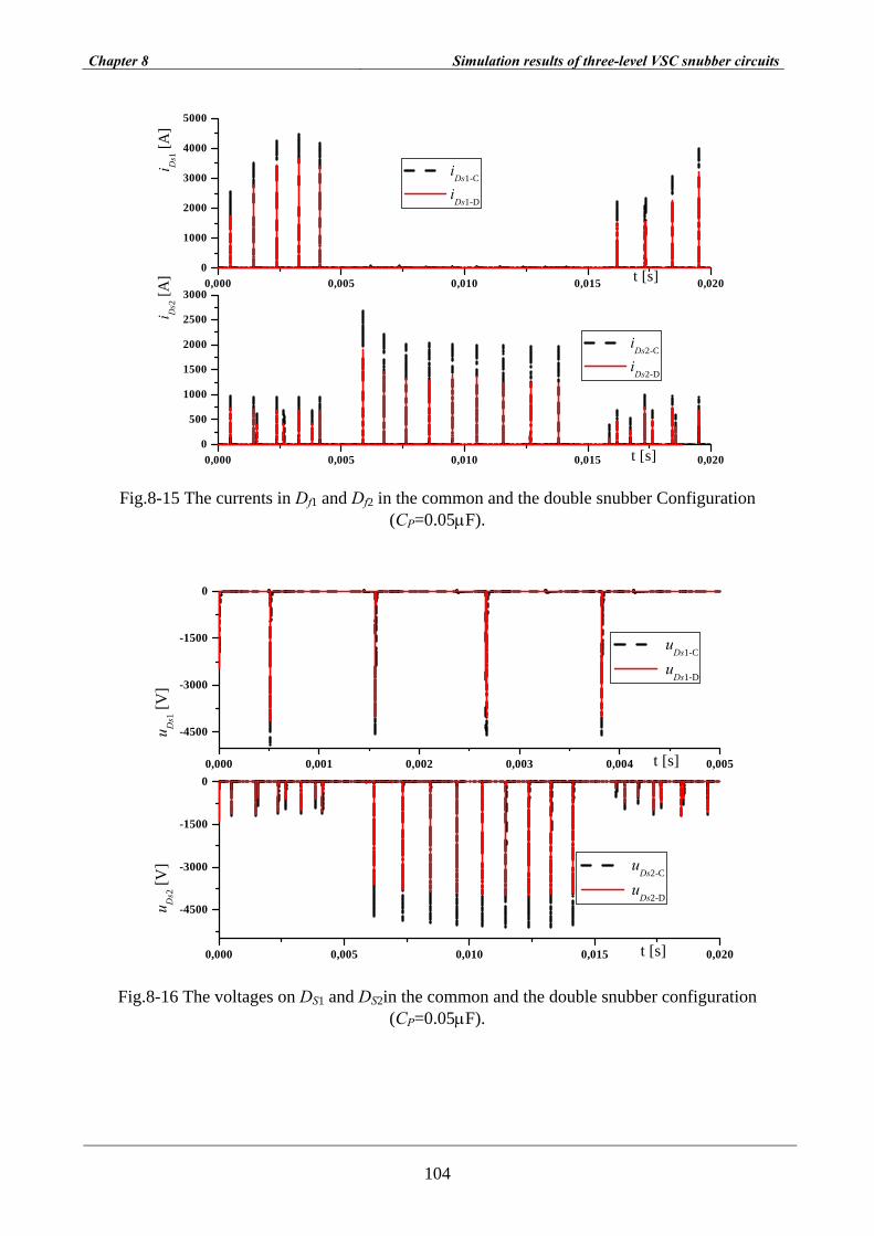
Chapter 8 Simulation results of three-level VSC snubber circuits
104
0,000 0,005 0,010 0,015 0,0200
500
1000
1500
2000
2500
30000,000 0,005 0,010 0,015 0,020
0
1000
2000
3000
4000
5000
iDs2-C
iDs2-D
i Ds2
[A]
t [s]
i Ds1
[A]
t [s]
iDs1-C
iDs1-D
Fig.8-15 The currents in Df1 and Df2 in the common and the double snubber Configuration (CP=0.05µF).
0,000 0,005 0,010 0,015 0,020
-4500
-3000
-1500
00,000 0,001 0,002 0,003 0,004 0,005
-4500
-3000
-1500
0
uDs2-C
uDs2-D
uD
s2 [V
]
t [s]
uD
s1 [V
]
t [s]
uDs1-C
uDs1-D
Fig.8-16 The voltages on DS1 and DS2in the common and the double snubber configuration (CP=0.05µF).

Chapter 8 Simulation results of three-level VSC snubber circuits
105
0,000 0,005 0,010 0,015 0,0200
1000
2000
3000
0,000 0,005 0,010 0,015 0,0200
1000
2000
3000
4000
5000
iDf2-C
iDf2-D i Df2 [A
]
t [s]
t [s]
i Df1 [A
]
iDf1-C
iDf1-D
Fig.8-17 The currents in DS1 and DS2 in the common and the double snubber configuration (CP=0.05µF).
0,000 0,005 0,010 0,015 0,0200
20000
40000
60000
80000
100000
120000
140000
Los
ses
[Ws/
p.u.
]
t [s]
con- Losses Double-Losses
Fig.8-18 The total losses (energy function) in RS1 in the conventional- and in RS1, RP1 in the proposed double snubber design over one cycle of the fundamental frequency (CP=0.05µF).
In the following figures, the effect of varying the CP to a smaller value is demonstrated (CP=0.01µF). Despite the additional reduction of the over-voltage and the current in the switching device GTO1 and GTO2 (Figs.8-19, 8-20), the effect on the over-voltage across GTO1 is small in comparison with the same parameter on GTO2 .But the current’s spikes are much smaller in the new design compared with the currents of GTO1, 2 in the common snubber circuit switching devices. The effect of changing the CP is much better visible in the time functions for the turn-off diode (Figs 8-

Chapter 8 Simulation results of three-level VSC snubber circuits
106
21, 8-22, and 8-23). This tendency also holds for the freewheel diode. Also, the total losses were fewer for the double snubber configuration than those in common snubber circuit (see Fig.8-24).
0,0050 0,0075 0,0100 0,0125 0,0150
6000
6250
65000,000 0,005 0,010 0,015 0,020
5000
5500
6000
6500
uGTO2-C
uGTO2-D
t [s]
uG
TO2 [V
]
t [s]
uG
TO1 [V
]
uGTO1-C
uGTO1-D
Fig.8-19 The voltages in GTO1 and GTO2 in the common and the double snubber
configuration (CP=0.01µF).
0,000 0,005 0,010 0,015 0,0200
1500
3000
4500
6000
0,000 0,005 0,010 0,015 0,0200
1500
3000
4500
6000
iGTO2-C
iGTO2-D
t [s]
i GTO
2 [A] t [s]
i GTO
1 [A]
iGTO1-C
iGTO1-D
Fig.8-20 The currents in GTO1 and GTO2 in the common and the double snubber configuration
(CP=0.01µF).

Chapter 8 Simulation results of three-level VSC snubber circuits
107
0,000 0,005 0,010 0,015 0,0200
500
1000
1500
2000
2500
30000,000 0,005 0,010 0,015 0,020
0
1000
2000
3000
4000
5000
iDs2-C
iDs2-D
i Ds2
[A]
t [s]
i Ds1
[A]
t [s]
iDs1-C
iDs1-D
Fig.8-21 The currents in DS1 and DS2 in the common and the double snubber configuration (CP=0.01µF).
0,000 0,005 0,010 0,015 0,020
-5000
-4000
-3000
-2000
-1000
00,000 0,001 0,002 0,003 0,004 0,005
-5000
-4000
-3000
-2000
-1000
0
uDs2-C
uDs2-D
uD
s2 [V
]
t [s]
uD
s1 [V
]
t [s]
uDs1-C
uDs1-D
Fig.8-22 The voltages on DS1 and DS2 in the common and the double snubber configuration (CP=0.01µF).

Chapter 8 Simulation results of three-level VSC snubber circuits
108
0,000 0,005 0,010 0,015 0,0200
1000
2000
3000
0,000 0,005 0,010 0,015 0,0200
1000
2000
3000
4000
iDf2-C
iDf2-D
t [s]
i Df2 [A
]
t [s]
i Df1
[A]
iDf1-C
iDf1-D
Fig.8-23 The currents in Df1and Df2 in the common and the double snubber Configuration (CP=0.01µF).
0,000 0,005 0,010 0,015 0,0200
25000
50000
75000
100000
125000
t [s]
Los
ses [
Ws/
p.u.
]
Losses-C Losses-D
Fig.8-24 The total losses (energy function) in RS1 in the conventional and in RS1, RP1 in the proposed double snubber design over two cycles of the fundamental frequency (CP=0.01µF).
8.7.2.1 Conclusion remarks The simulation results show that the proposed double snubber configuration facilitates reducing
the stress in the switching device (e.g. GTO’s) as well as the other semiconductor devices in the form of the turn-off and the freewheel diodes. The dependency on the capacitance of the additional snubber parts is visible but not extremely strong. Therefore, rather small, cheap, and economical elements should be able to provide this additional advantageous effect. The new double snubber circuit is suitable for high voltage and high power more level converter systems and FACTS

Chapter 8 Simulation results of three-level VSC snubber circuits
109
systems. The advantages of the new design is the ability to minimize both, the over voltage and the losses in the entire circuit by using an additional parallel RC damping snubber. Therefore, the additional RC circuit can compensate the disadvantage of the conventional RCD snubber design, that the effective value for RS during the charging of snubber capacity CS is essentially zero. But the main cost of the snubber circuit will be high compared with the common snubber circuit design while the number of passive elements is large.
8.7.3 Comparing the common and the optimized snubber design In this simulation, a comparison between the common snubber circuit and the optimized
snubber design was done. The element parameters were chosen in the same way, the only different is that the value of capacitor CS was reduced to other values (see Table 8.6) in the simulation, while this reduction improves the performance of the optimized snubber design in the direction of reduced losses and the over-voltage across the power switching device. The load and source data will be the same as in Table 8.4
Snubber circuit data Optimized snubber design Common snubber
CS (µF) 1 0.5 0.25 1
RS (Ω) 5 5 2 5
Table 8.6 the snubber circuits (common and design) information.
In the following Figures, the stresses in different semiconductor devices (GTOs and diodes) will be analyzed for CS =1µF. Figs 8-25 and 8-26 show that the over-voltages across and the currents in GTO1 and GTO2. The over-voltages across GTO1, 2 are limited in a better way by the optimized snubber than the common snubber design during the turn-off process, and the current spikes are also much smaller in GTO2 and about the same in GTO1 than those in the common snubber circuit as shown in Fig.8-25.
0,0050 0,0075 0,0100 0,0125 0,01506000
6250
65000,000 0,005 0,010 0,015 0,020
5750
6000
6250
6500
t [s]
uG
TO2 [V
]
uGTO2-C
uGTO2-Opti
t [s]
uG
TO1 [V
]
uGTO1-C
uGTO1-Opti
Fig.8-25 The voltages in GTO1 and GTO2 in the common and the optimized snubber design.

Chapter 8 Simulation results of three-level VSC snubber circuits
110
Figs.8-27, 8-28 and 8-29 show the voltages and the currents in diodes DS1 and Don1 and the total losses as an energy function. It can easily be seen, that the currents resulting from the optimized snubber design are more adequate than those simulated for the common snubber circuit, especially in the turn-off diode DS1 and turn-on diode Don1. The current in freewheel diode Df1 is about the same but in Df2 the current in the optimized snubber circuit design is clearly smaller the common snubber circuit (see Fig.8-24(a)).
0,000 0,005 0,010 0,015 0,0200
1500
3000
4500
6000
0,000 0,005 0,010 0,015 0,0200
2500
5000
7500
iGTO2-C
iGTO2-Opti
t [s]
i GTO
2 [A]
iGTO1-C
iGTO1-Opti
t [s]
i GTO
1 [A]
Fig.8-26 The currents in GTO1 and GTO2in the common and the optimized snubber design.
0,000 0,005 0,010 0,015 0,0200
50000
100000
150000
0,000 0,005 0,010 0,015 0,0200
1000
2000
3000
0,000 0,005 0,010 0,015 0,0200
2000
4000
6000
t [s]
Los
ses [
Ws/
p.u.
]
Losses-C Losses-Opti
(a)
(b)
t [s]
i Df2 [A
] iDf2-C iDf2-Opti
t [s]
i Df1 [A
]
iDf1-C iDf1-Opti
Fig.8-27 (a) The currents in Df1 and Df2 and comparing the total losses in conventional and (b)
the optimised snubber configuration (energy function).

Chapter 8 Simulation results of three-level VSC snubber circuits
111
0,000 0,005 0,010 0,015 0,0200
1500
3000
45000,000 0,005 0,010 0,015 0,020
0
1500
3000
4500
t [s]
i Don
1 [A]
iDon1-C
iDon1-Opti
t [s]
i Ds1
[A]
iDs1-C
iDs1-Opti
Fig.8-28 The current in DS1 and Don1 in the common and the optimized snubber configuration.
The over-voltages across Don1 and DS1 are the same as shown in the two snubber circuit as presented in Fig 8-29. The total losses in the circuit (GTO, diode and snubber element losses) for the two different snubber designs (conventional snubber circuit and optimized snubber design) are illustrated in Fig.8-27(b). The losses are shown as an energy function over one cycle of the fundamental frequency. As indicated, the energy lost in converters based on the optimized snubber design is much lower than that dissipated in the common snubber design.
0,000 0,005 0,010 0,015 0,020
-6000
-4500
-3000
-1500
00,000 0,005 0,010 0,015 0,020
-4500
-3000
-1500
0
uD
on1 [V
]
t [s]
uDon1-C
uDon1-Opti
uD
s1 [V
]
t [s]
uDs1-C
uDs1-Opti
Fig.8-29 The voltages in DS1 and Don1 in the common and the optimized snubber
configuration.

Chapter 8 Simulation results of three-level VSC snubber circuits
112
In the next two simulations, CS was set to 0.5µF and then 0.25µF. Figs 8-30 to 8-34 present the simulation results for the value of CS. Figs 8-30 and 8-31 show the voltage and the current resulting in GTO1,2. The over-voltage shown in Fig.8-30 across GTO1 and GTO2 in the optimized snubber design is more limited than it is in the common snubber design and the current spikes through GTO2 are much smaller as presented in Fig.8-31.
0,0050 0,0075 0,0100 0,0125 0,0150
6000
6250
65000,000 0,005 0,010 0,015 0,020
5000
5500
6000
6500
t [s]
uG
TO2 [V
]
uGTO2-C
uGTO2-Opti
t [s]
uG
TO1 [V
]
uGTO1-C
uGTO1-Opti
Fig.8-30 The voltages on GTO1 and GTO2 in the common and the optimized snubber design
(CS=0.5µF, RS=5Ω).
0,000 0,005 0,010 0,015 0,0200
2000
4000
6000
0,000 0,005 0,010 0,015 0,0200
2000
4000
6000
8000
iGTO2-C
iGTO2-Opti
t [s]
i GTO
2 [A]
iGTO1-C
iGTO1-Opti
t [s]
i GTO
1 [A]
Fig.8-31 The currents in GTO1 and GTO2 in the common and the optimized snubber design
(CS=0.5µF, RS=5Ω).
The currents through freewheel-, turn-off and turn-on diodes are better improved in the optimized snubber design than in the common snubber circuit. Fig.8-32 shows currents through DS1
and Don1, and Fig.8-34(a) illustrates the current of Df1,2. The over-voltage across the DS1 and Don1 in

Chapter 8 Simulation results of three-level VSC snubber circuits
113
the optimized snubber design becomes more acceptable than the same voltage in the common snubber circuit comparatively with the result of the last simulation as clarified in Fig.8-33.The total losses in the optimized snubber design and the common snubber circuit are compared as an energy function over one cycle of the fundamental frequency in Fig.8-34(b).
0,000 0,005 0,010 0,015 0,0200
1500
3000
4500
0,000 0,005 0,010 0,015 0,0200
1500
3000
4500
t [s]
i Don
1 [A]
iDon1-C
iDon1-Opti
t [s]
i Ds1
[A]
iDs1-C
iDs1-Opti
Fig.8-32 Currents in DS1 and Don1 in the common and the optimized snubber configuration (CS=0.5µF, RS=5Ω).
0,000 0,005 0,010 0,015 0,020
-6000
-4500
-3000
-1500
00,000 0,005 0,010 0,015 0,020
-4500
-3000
-1500
0
uD
on1 [V
]
t [s]
uDon1-C
uDon1-Opti
uD
s1 [V
]
t [s]
uDs1-C
uDs1-Opti
Fig.8-33 Voltages on DS1 and Don1 in the common and the optimized snubber configuration (CS=0.5µF, RS=5Ω).

Chapter 8 Simulation results of three-level VSC snubber circuits
114
0,000 0,005 0,010 0,015 0,0200
50000
100000
1500000,000 0,005 0,010 0,015 0,020
0
1000
2000
3000
0,000 0,005 0,010 0,015 0,0200
2000
4000
6000
t [s]
Los
ses [
Ws/
p.u.
]
Losses-C Losses-Opti
t [s]
i Df2 [A
] iDf2-C iDf2-Opti
t [s]
i Df1 [A
] iDf1-C iDf1-Opti
(a)
(b)
Fig.8-34 (a) The currents in Df2 and Df2 in the common and the optimized snubber configuration, and (b) the comparison of the total losses in the conventional and the optimized
snubber configuration (energy function) (CS=0.5µF, RS=5Ω).
As mentioned before, the total energy lost in the optimized snubber design in this simulation is much lower than in the common snubber circuit. One of the reasons therefore is that the losses are related to the capacitor CS. Also, the losses in the GTO’s itself are less for the optimized snubber design but the difference here is not so much. For the other value of (CS =0.25µF), the performance of the optimizer snubber will be more typical, especially in the over-voltage protection and minimization of the total losses. Fig.8-35 and Fig.8-36 show the effect of CS reduction, the over-voltage becomes smaller and also the spikes in the current for GTO1,2.
The current of freewheel diodes and total losses energy function are presented in Fig.8-37. The current in Df1 in the optimizer snubber design has about the same value, but in Df2 the current is smaller in comparison of the common snubber circuit, while the total losses are clearly smaller than these of the common snubber circuit.
Based on the aforementioned results, the optimized snubber design is based on a new and simple structured snubber, which depends on passive elements. As a result, the number of required components is reduced, and the reliability increases distinctly. The presented optimized snubber design provides several additional advantages: It increases the optional performance of the three level converters due to the lower clamping over-voltages across the switching devices, it improves the efficiency because of the lower snubber and total losses, its suitable structure can be extended to

Chapter 8 Simulation results of three-level VSC snubber circuits
115
energy recovery snubbers and there is no unbalance problem. Additionally, the manufacturing costs, the complexity and therefore the converter size can be reduced.
0,0050 0,0075 0,0100 0,0125 0,0150
6000
6250
65000,000 0,005 0,010 0,015 0,020
5750
6000
6250
6500
t [s]
uG
TO2 [V
]
uGTO2-C uGTO2-Opti
t [s]
uG
TO1 [V
]
uGTO1-C
uGTO1-Opti
Fig.8-35 The voltages in GTO1 and GTO2 in the common and the optimized snubber design (CS=0.25µF, RS=2Ω).
0,000 0,005 0,010 0,015 0,0200
1500
3000
4500
6000
0,000 0,005 0,010 0,015 0,0200
1500
3000
4500
6000
7500
iGTO2-C
iGTO2-Opti
t [s]
i GTO
2 [A]
iGTO1-C
iGTO1-Opti
t [s]
i GTO
1 [A]
Fig.8-36 The currents in GTO1 and GTO2 in the common and the optimized snubber design (CS=0.25µF, RS=2Ω).

Chapter 8 Simulation results of three-level VSC snubber circuits
116
0,000 0,005 0,010 0,015 0,0200
50000
100000
150000
0,000 0,005 0,010 0,015 0,0200
1500
3000
0,000 0,005 0,010 0,015 0,0200
1500
3000
4500
t [s]
Los
ses [
ws/
p.u.
]
Losses-C Losses-Opti
(a)
(b)
t [s]
i Df2 [A
] iDf2-C
iDf2-Opti
t [s]
i Df1 [A
] iDf1-C
iDf1-Opti
Fig.8-37 (a) The currents in Df2 and Df2 in the common and the optimized snubber
configuration, and (b) the comparison of the total losses in the conventional and the optimized snubber configuration (energy function) (CS=0.25µF, RS=2Ω).
8.7.4 Comparison of the common and the dual-use snubber circuits for different values for CS-D
In the first simulation, a comparison between the common snubber circuit and the dual-use snubber design will be done. Two different scenarios were analyzed as follow: In the first, the parameters were defined by maximum values for modern power semiconductor device for an MV inverter system. The turn-off snubber parameters were set to the standard parameter values and other values (see Table 8.4 and Table 8.7) while the load current will be IL= 5000A to get the optimal values for the snubber circuit elements.
Snubber circuit data Dual-use snubber design Common snubber
CS (µF) 0.5 0.25 1
RS (Ω) 2.5 2.5 5
Table 8.7 Snubber circuits (common and double dual-use) information.
In the following figures the stresses for different power semiconductor devices (GTOs and diodes) will be discussed and analyzed. Fig.8-38 and Fig.8-39 show that the voltages and the current in GTO1, 2 in the two circuits, the over-voltage (shown in Fig.8-38) is limited in a better way by the dual-use snubber circuit and the current pecks are smaller as presented in Fig.8-39.

Chapter 8 Simulation results of three-level VSC snubber circuits
117
Figs.8-40 and 8-41 present the current and the voltage in DS1 and Don1. It is explicitly seen that the currents in DS1 and Don1 in the dual-use snubber circuit are smaller than those of the common snubber circuit. The voltage in the diode in the dual-use snubber circuit is suppressed much more than the common snubber circuit. For the free-wheel diodes, it can be see that the currents of freewheel diodes resulting from the dual-use snubber circuit are more favorable than those of the simulated for the common snubber circuit as shown in Fig.8-42(a).
0,0050 0,0075 0,0100 0,0125 0,0150
6000
6200
6400
0,000 0,005 0,010 0,015 0,020
5800
6000
6200
6400
t [s]
uG
TO2 [V
] uGTO2-C
uGTO2-Dual
uG
TO1 [V
]
t [s]
uGTO1-C
uGTO1-Dual
Fig.8-38 The voltages on GTO1 and GTO2 in the common and the dual-use snubber configuration (CS-D=0.5µF, RS=2.5Ω).
0,000 0,005 0,010 0,015 0,0200
1500
3000
4500
60000,000 0,005 0,010 0,015 0,020
0
1500
3000
4500
6000
7500
t [s]
i GTO
2 [A]
iGTO2-C
iGTO2-Dual
i GTO
1 [A]
t [s]
iGTO1-C
iGTO1-Dual
Fig.8-39 The currents in GTO1 and GTO2 in the common and the dual-use snubber
configuration (CS-D=0.5µF, RS=2.5Ω).

Chapter 8 Simulation results of three-level VSC snubber circuits
118
0,000 0,005 0,010 0,015 0,0200
1500
3000
4500
0,000 0,005 0,010 0,015 0,0200
1500
3000
4500
t [s]
i Don
1 [A]
iDon1-C
iDon1-Dual
t [s]
i Ds1
[A]
iDs1-C
iDs1-Dual
Fig.8-40 The currents in DS1 and Don1 in the common and the dual-use snubber configuration (CS-D=0.5µF, RS=2.5Ω).
In Fig.8-42(b), the total losses in the power semiconductor devices and in RSµ in the two inverters are compared as energy function over one cycle of the fundamental frequency.
0,000 0,005 0,010 0,015 0,020
-6000
-4500
-3000
-1500
00,000 0,005 0,010 0,015 0,020
-4500
-3000
-1500
0
uD
on1 [V
]
t [s]
uDon1-C
uDon1-Dual
t [s]
uD
s1 [V
]
uDs1-C
uDs1-Dual
Fig.8-41 The voltages in DS1 and Don1 in the common and the dual-use snubber configuration
(CS-D=0.5µF, RS=2.5Ω).

Chapter 8 Simulation results of three-level VSC snubber circuits
119
0,000 0,005 0,010 0,015 0,0200
50000
100000
150000
0,000 0,005 0,010 0,015 0,0200
1500
3000
45000,000 0,005 0,010 0,015 0,020
0
1500
3000
4500
(b) t [s]
Los
ses [
Ws/
p.u.
]
Losses-C Losses-Dual
(a)
iDf2-C
iDf2-Dual
t [s]
i Df2 [A
]
t [s]
i Df1 [A
] iDf1-C
iDf1-Dual
Fig.8-42 (a) The currents in Df2 and Df2 in the common and dual-use snubber configuration, and (b) comparison of the total losses in the conventional and the optimized snubber
configuration (energy function) (CS-D=0.5µF, RS=2.5Ω).
As indicated, the energy lost in the entire power semiconductor device and snubber circuit resistors in the dual-use snubber circuit is much lower than that in the common snubber circuit. Also, the losses in the GTO’s itself are less for the dual-use snubber circuit but do not differ too much.
This next simulation was carried out for a small value of CS-D = 0.25µF and RS-D = 2.5 Ω. The simulation results are analyzed as the following: Figs 8-43 and 8-44 illustrate the voltages and the current in GTO1 and GTO2. The over-voltage across the GTOµ is limited much better, and the peak of current is smaller than the first simulation. For the turn-off diode, the over-voltages across DS1, Don1 are also less than in the first simulation; the currents have the same advantages (see Fig.8.-45 and Fig.8-46). The currents in the freewheel diodes Df1 and Df2 are more adequate as shown in Fig.8-47(a), in which the current in Df2 is smaller than the same current in the other simulation. The total losses are illustrated in Fig.8-47(b) as energy function: The total energy lost in the inverters based on the dual-use snubber circuit is lower than that dissipated in the common snubber circuit.

Chapter 8 Simulation results of three-level VSC snubber circuits
120
0,0050 0,0075 0,0100 0,0125 0,0150
6000
6250
65000,000 0,005 0,010 0,015 0,020
5750
6000
6250
6500
t [s]
uG
TO2 [V
]
uGTO2-C
uGTO2-Dual
t [s]
uG
TO1 [V
] u
GTO1-C
uGTO1-Dual
Fig.8-43 The voltages in GTO1 and GTO2 in the common and the dual-use snubber configuration (CS-D=0.25µF, RS=2.5Ω).
0,000 0,005 0,010 0,015 0,0200
1500
3000
4500
60000,000 0,005 0,010 0,015 0,0200
1500
3000
4500
6000
t [s]
i GTO
2 [A]
iGTO2-C
iGTO2-Dual
t [s]
i GTO
1 [A]
iGTO1-C
iGTO1-Dual
Fig.8-44 The currents in GTO1 and GTO2 in the common and the dual-use snubber configuration (CS-D=0.25µF, RS-D =2.5Ω).

Chapter 8 Simulation results of three-level VSC snubber circuits
121
0,000 0,005 0,010 0,015 0,0200
1500
3000
4500
0,000 0,005 0,010 0,015 0,0200
1500
3000
4500
t [s]
i Don
1 [A]
iDon1-C
iDon1-Dual
t [s]
i Ds1
[A]
iDs1-C
iDs1-Dual
Fig.8-45 The voltages in DS1 and Don1 in the common and the dual-use snubber configuration (CS-D=0.25µF, RS-D =2.5Ω).
0,000 0,005 0,010 0,015 0,020
-6000
-4500
-3000
-1500
00,000 0,005 0,010 0,015 0,020
-4500
-3000
-1500
0
t [s]
uD
on1 [V
]
uDon1-C
uDon1-Dual
t [s]
uD
s1 [V
] uDs1-C
uDs1-Dual
Fig.8-46 The voltages in DS1 and Don1 in the common and the dual-use snubber configuration (CS-D=0.25µF, RS-D=2.5Ω).
Based on the aforementioned results, an optimized snubber design is proposed to be used in high voltage and high power more-level converter systems and partially in FACTS devices. The

Chapter 8 Simulation results of three-level VSC snubber circuits
122
main advantage of the new design is the simple structure snubber circuit, which realizes the facility to minimize the over-voltage, the total losses in the entire circuit, no unbalance problems and the manufacturing costs of the snubber circuit. Using a Matlab®/ SimulinkTM simulation based on an MV three-level inverter system, the over-voltages and the losses are compared between the common and the dual-use snubber circuits. The results clarify the features of the dual-use snubber circuit especially for the operation close to the limits of the SOA (Safe Operation Area).
0,000 0,005 0,010 0,015 0,0200
50000
100000
1500000,000 0,005 0,010 0,015 0,020
0
1500
3000
45000,000 0,005 0,010 0,015 0,020
0
1500
3000
4500
(b) t [s]
Los
ses [
Ws/
p.u.
] Losses-C Losses-Dual
(a) t [s]
i Df2 [A
] iDf2-C
iDf2-Dual
t [s]
i Df1 [A
]
iDf1-C
iDf1-Dual
Fig.8-47 (a) The currents in Df2 and Df2 in the common and dual-use snubber configuration and (b) comparison between the total losses in the conventional and the optimized snubber
configuration (energy function) (CS-D=0.25µF, RS-D=2.5Ω).
8.7.5 Comparison of the dual-inductive- and common snubber circuit The simulation will be performed for the standard parameters and another selected optimized
values for the dual-inductive snubber circuit and the common snubber circuit design. The values of the parameters were set to the standard values for the common snubber circuit and the dual-inductive snubber for the first simulation. In the second simulation the parameters of the dual-inductive snubber were modified to the next values CS=0.25µF and RS=2.5Ω, but the load characteristics were the same as in the last comparison. Figs 8-48 and 8-49 show the voltages and the current in GTO1 and GTO2. The over-voltages across GTOs in the dual-inductive snubber circuit are suppressed to save values in comparison with the common snubber circuit. Because the reason of the over-voltage “RON and stray inductance” have very small effect as discussed before. While, the parallel inductive limits the di/dt, makes the effect RON smaller, and absorbs the total energy in the turn-on snubber circuit, the current spikes are also restricted from those of the common snubber

Chapter 8 Simulation results of three-level VSC snubber circuits
123
circuit. The voltage across DS1 is less than the common snubber circuit, but the over-voltage across the turn-on diode Don1 is a bit bigger than the same diode in the common snubber circuit, because the Don1-D-Ind has now two functions: turn-on and turn-off diode (see Fig.8-50).
0,0050 0,0075 0,0100 0,0125 0,0150
6000
6200
6400
0,000 0,005 0,010 0,015 0,0205800
6000
6200
6400
t [s]
uG
TO2 [V
]
uGTO2-C
uGTO2-D-Ind
uG
TO1 [V
]
t [s]
uGTO1-C
uGTO1-D-Ind
Fig.8-48 The voltages on GTO1 and GTO2 in the common and the Dual-indicative Snubber
design (Ed=6000V, IL=5000A, CS=0.25µF, RS=2.5Ω).
0,000 0,005 0,010 0,015 0,0200
1000
2000
3000
4000
5000
6000
0,000 0,005 0,010 0,015 0,0200
1000
20003000
400050006000
t [s]
i GTO
2 [A]
iGTO2-C
iGTO2-D-Ind
t [s]
i GTO
1 [A]
iGTO1-C
iGTO1-D-Ind
Fig.8-49 The currents in GTO1 and GTO2 in the common and the Dual-indicative Snubber
design (Ed=6000V, IL=5000A, CS=0.25µF, RS=2.5Ω).
For other simulations parameters, Fig.8-51 presents the currents in DS1 and Don1 in the two snubber circuits; it is clearly that the current in DS1 in the new snubber circuit is smaller than the other snubber circuit. The current value depends on the capacitor value and the performance of the

Chapter 8 Simulation results of three-level VSC snubber circuits
124
turn-off snubber circuit. For the turn-on diode current iDon1, the effect of the parallel inductive is abundantly clear, this current is produced from the stored energy in the turn-on and stray inductors, so we can get more recovery energy from the turn-on snubber circuit by using recovery transformer depending on that the inverter efficiency will be high and the losses will be smaller than that those of the common snubber circuit.
0,000 0,005 0,010 0,015 0,020
-5000
-4000
-3000
-2000
-1000
0
0,000 0,005 0,010 0,015 0,020
-6000-5000-4000
-3000-2000
-10000
t [s]
uD
s1 [V
]
uDs1-C
uDs1-D-Ind
t [s]
uD
on1 [V
] uDon-C
uDon1-D-Ind
Fig.8-50 The voltages on DS1 and Don1 in the common and the Dual-indicative Snubber design
(Ed=6000V, IL=5000A, CS=0.25µF, RS=2.5Ω).
0,000 0,005 0,010 0,015 0,0200
1000
2000
3000
4000
5000
0,000 0,005 0,010 0,015 0,0200
1000
2000
3000
4000
5000
t [s]
i Ds1
[A]
iDs1-C
iDs1-D-Ind
i Don
1 [A]
t [s]
iDon1-C
iDon1-D-Ind
Fig.8-51 The currents in DS1and Don1 in the common and the Dual-indicative Snubber design (Ed=6000V, IL=5000A, CS=0.25µF, RS=2.5Ω).

Chapter 8 Simulation results of three-level VSC snubber circuits
125
The freewheel diodes current and the losses energy function are shown in Fig.8-52; the Dfµ currents in new design is smaller than the other snubber circuit (Fig.8-52(a)), and the total losses energy function for the dual-inductive snubber circuit is under the other function, this result comes from the big influence of the new snubber circuit design .
0,000 0,005 0,010 0,015 0,0200
50000
100000
1500000,000 0,005 0,010 0,015 0,0200
50010001500200025003000
0,000 0,005 0,010 0,015 0,0200
10002000300040005000
(b) t [s]
Los
ses [
Ws/
p.u.
]
Losses-C Losses-D-Ind
t [s]
i Df2 [A
]
iDf2-C
iDf2-D-Ind
t [s]
i Df1 [A
] iDf1-C
iDf1-D-Ind
Fig.8-52 (a) The currents in Df2 and Df2 in the common and the Dual-indicative snubber design and (b) comparison of the total losses in the conventional and the optimized snubber
configuration (energy function) (Ed=6000V, IL=5000A, CS=0.25µF, RS=2.5Ω).
This simulation gives an evolution of the common and dual-inductive snubber circuits. The dual-inductive snubber circuit represents a compromise between snubber size, the number of devices which compose the snubber circuit, and the total losses in the snubber circuit and in the power switching devices. This choice will be suitable and fitting for the high voltage and FACTS systems, because it has permitted losses, the complexity of the circuit, and the weight and the size of the snubber circuit.

Chapter 9 Experimental investigation on the dual snubber circuit design
126
9 Experimental investigation on the dual snubber circuit design
9.1 Introduction For the testing the dual snubber circuit design, a three-level inverter system consisting of four
IGBT transistors, including the protection circuits has been established. To drive this circuit during the test and prototyping phases, two possibilities were available. The first was to use a computer program named D-Link. The D-Link takes the simulation output waveforms from Matlab®/SimulinkTM and generates these waveforms on the serial port of the PC. This cheap solution was not chosen because D-Link can generate a minimum pulse width of 100 microseconds while the minimum pulse width required for the driving signals is 500 nanoseconds. The alternative was using complex programmable logic devices (CPLDs) available from Lattice Semiconductor Corporation. Even though this solution moves expensive, the CPLDs can be used in the prototyping phases of future projects. This will distribute the CPLDs cost over many projects and hence makes this solution feasible. The ispMach4A5 CPLD series was used in the signal generator circuit. In principle series can generate pulse widths of 5ns and hence it satisfies the required minimum pulse width constraint. The driving circuit logic was designed and verified using the ispDesignExpert from Lattice. It contains a schematic editor and a simulator in addition to other utilities. The designed logic was then programmed into the CPLDs using Lattice-Pro software.
9.2 Design Procedure The design of the drive circuit of the inverter system will be in three steps as in the following:
• The first step was to get the needed IGBT-driving pulses that will be generated. The signals where taken from Matlab®/SimulinkTM simulations of the real system at 900 Hz switching frequency. The minimization of the switching frequency from the standard 3 kHz to only 900 Hz was made in order to minimize the logic complexity of the driving circuit so it can fit into only one CPLD. The simulation results of Matlab®/SimulinkTM are drawn in Fig. 9-1.
0,00 0,01 0,02 0,03 0,040,00,20,40,60,81,0
0,00 0,01 0,02 0,03 0,040,00,20,40,60,81,0
0,00 0,01 0,02 0,03 0,040,00,20,40,60,81,0
0,00 0,01 0,02 0,03 0,040,00,20,40,60,81,0
G4
t [s]
t [s]
G3
G2
t [s]
t [s]
Gat
e4G
ate3
Gat
e2G
ate1 G1
Fig.9-1 Pulse scheme of Matlab®/SimulinkTM at 900Hz
• The second step was to build the needed generating logic in the CPLDs software. The

Chapter 9 Experimental investigation on the dual snubber circuit design
127
schematic of the logic circuit was drawn using ispDesignExpert from Lattice. The ispDesignExpert contains a schematic editor and a functional and timing simulator. The schematic of the logic circuit is shown in Fig. 9-2 and the functional simulation results are presented in Fig. 9-3. After the simulating of the circuit, a JEDEC-file (*.jed) will be generated. The JEDEC file contains the needed information which will configure the CPLD according to the designed logic circuit.
Fig. 9-2: The schematic diagram of the driving circuit logic.
• The last step was to transfer the program to the CPLD, then test it with and without the optocoupler system, finally put them together on the same board as shown in Fig. 9-4.

Chapter 9 Experimental investigation on the dual snubber circuit design
128
Fig. 9-3: Functional simulation results from the ispDesignExpert.
Fig. 9-4: The driving circuit including: (a) The 5 and 15 V power supply from a 12 V source (b) CPLD Chip and (c) 4 optocoupler.
9.3 Driving the IGBT bridge circuit The signals that must be generated to drive the IGBT bridge circuit are shown in Fig. 9-3 and
redrawn with a bigger scale in Fig. 9-5 for discussing its characteristic.
Fig. 9-5 One period of the driving signals.
(a)
(b)
(c)
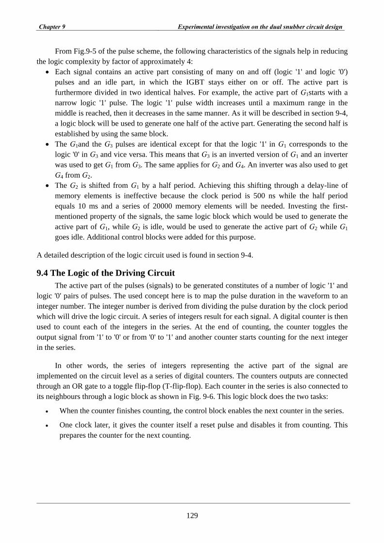
Chapter 9 Experimental investigation on the dual snubber circuit design
129
From Fig.9-5 of the pulse scheme, the following characteristics of the signals help in reducing the logic complexity by factor of approximately 4:
• Each signal contains an active part consisting of many on and off (logic '1' and logic '0') pulses and an idle part, in which the IGBT stays either on or off. The active part is furthermore divided in two identical halves. For example, the active part of G1starts with a narrow logic '1' pulse. The logic '1' pulse width increases until a maximum range in the middle is reached, then it decreases in the same manner. As it will be described in section 9-4, a logic block will be used to generate one half of the active part. Generating the second half is established by using the same block.
• The G1and the G3 pulses are identical except for that the logic '1' in G1 corresponds to the logic '0' in G3 and vice versa. This means that G3 is an inverted version of G1 and an inverter was used to get G1 from G3. The same applies for G2 and G4. An inverter was also used to get G4 from G2.
• The G2 is shifted from G1 by a half period. Achieving this shifting through a delay-line of memory elements is ineffective because the clock period is 500 ns while the half period equals 10 ms and a series of 20000 memory elements will be needed. Investing the first-mentioned property of the signals, the same logic block which would be used to generate the active part of G1, while G2 is idle, would be used to generate the active part of G2 while G1 goes idle. Additional control blocks were added for this purpose.
A detailed description of the logic circuit used is found in section 9-4.
9.4 The Logic of the Driving Circuit The active part of the pulses (signals) to be generated constitutes of a number of logic '1' and
logic '0' pairs of pulses. The used concept here is to map the pulse duration in the waveform to an integer number. The integer number is derived from dividing the pulse duration by the clock period which will drive the logic circuit. A series of integers result for each signal. A digital counter is then used to count each of the integers in the series. At the end of counting, the counter toggles the output signal from '1' to '0' or from '0' to '1' and another counter starts counting for the next integer in the series.
In other words, the series of integers representing the active part of the signal are implemented on the circuit level as a series of digital counters. The counters outputs are connected through an OR gate to a toggle flip-flop (T-flip-flop). Each counter in the series is also connected to its neighbours through a logic block as shown in Fig. 9-6. This logic block does the two tasks:
• When the counter finishes counting, the control block enables the next counter in the series.
• One clock later, it gives the counter itself a reset pulse and disables it from counting. This prepares the counter for the next counting.

Chapter 9 Experimental investigation on the dual snubber circuit design
130
Fig. 9-6: The logic block schematic diagram.
The series of counters counts continuously. The counting begins with first counter in the series (first_1 output in Fig. 9-7), continues until the tenth forming the first half of active period (forward counting). Backward counting starts directly that after and continues until the first counter (first_2 output in Fig. 9-7). Each forward and backward run of the counters in the series generates on active part. The control block shown in Fig. 9-7 switches the output signal between the T-flip-flop dedicated to generate G1 and the T-flip-flop dedicated to generate G2. When the active part of, say, G1 is being generated, the G2 flip-flop keeps its last state, and hence, the idle part is generated automatically.
One problem arises at the two ends of the counters' series. The first counter must count twice, one in the forward counting and one in the backward counting. Instead of, two identical counters (with first_1 and first_2 outputs in Fig. 9-7) were used. The count of the last counter in series (tenth output) was doubled to generate the wide pulse in the middle of the active part as shown in Fig. 9-5.
Fig. 9-7: Control block of the driving circuit.

Chapter 9 Experimental investigation on the dual snubber circuit design
131
9.5 Output Circuit The driving circuit consists of the ispMach4A5 128/256 CPLD from Lattice Semiconductor
Co. and four optocouplers, the HCPL 316J, one for each of the driving signals. The CPLD was programmed to generate the signals G1, G2, G3, and G4. The optocouplers serve two purposes:
• Affording electrical ground isolation between the CPLD side and the IGBTs side. This is important to protect the CPLD from the spikes that may be generated during high-speed switching of the IGBTs.
• Making the interface between the 5V logic levels at the CPLD side and the less than 12V driving levels at the IGBTs side.
9.6 Experimental results Three-level IGBTs (MG150J2YS1, CM100DU-12F) inverter system was constructed for
testing the performance of the dual-use and dual-inductive snubber circuit design especially in the protection from over-voltage across the power switching devices (see Fig-8-7). The parameters of the inverter system and the load information are shown in Table 9-1, the power factor of the loads is Pf =0.8. The total test system consists of: adjustable transformer supplies the three-phase diode bridge-rectifier, the rectifier is connected to two capacitors (DC-link) which is coupled to the three-level IGBT inverter system, the inverter will be loaded with ohmic- and inductive-burden. The voltage will be measured across the IGBTs, snubber-diode and the load, and so the load current. The measuring system consists of amplifier; oscilloscope, ampere meter, current-transformer and voltmeter (see Fig 9-8).
CS [µF] RS [Ω] LON [µH] RON [Ω] LP [µH] IO [A] Rload [Ω] Lload [mH]
0.47 33 1 0.33 2 0.5 50,66 121,31
Table 9.1 Dual-use- and dual-inductive snubber circuits information.
3 ~
Loa
d
3 level IGBTinverter system
Diode bridgerectiefer Vin1
Vin2
Vout1
Vout1
Vout2
Vout2
Driver
0
0
0
0
0
Amplifier
Fig. 9-8 Control blocks of the complete Three-level IGBT inverter system.
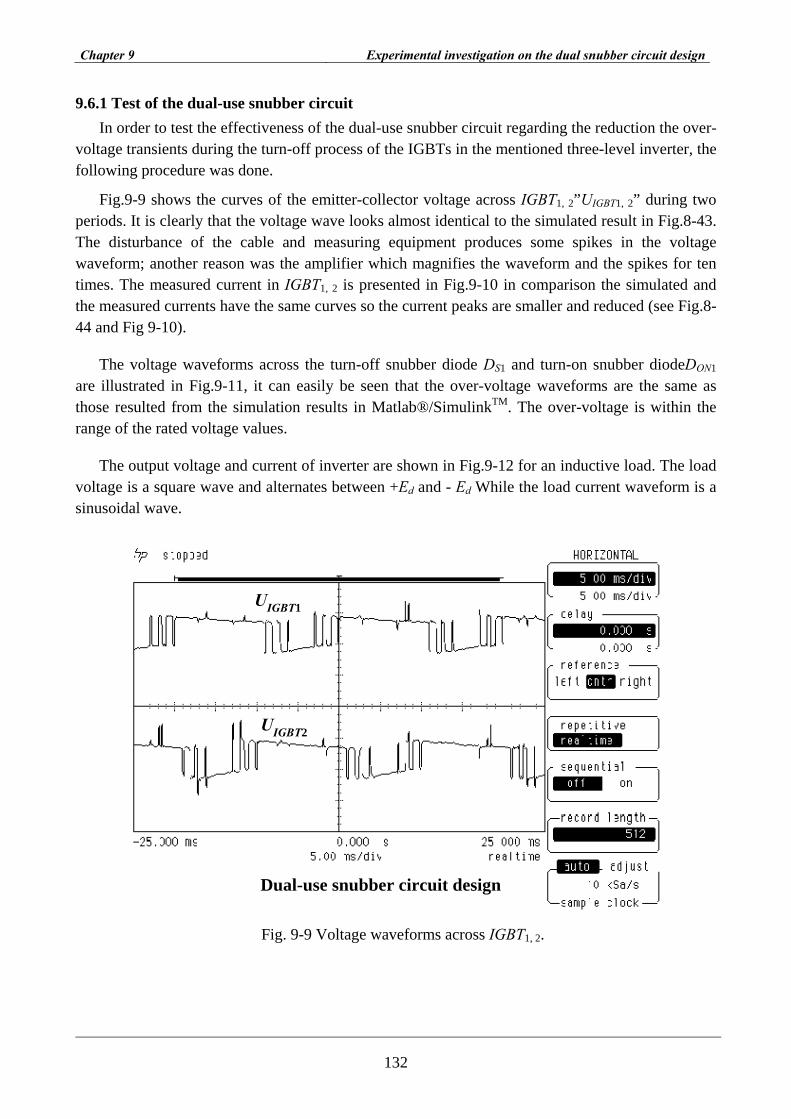
Chapter 9 Experimental investigation on the dual snubber circuit design
132
9.6.1 Test of the dual-use snubber circuit In order to test the effectiveness of the dual-use snubber circuit regarding the reduction the over-
voltage transients during the turn-off process of the IGBTs in the mentioned three-level inverter, the following procedure was done.
Fig.9-9 shows the curves of the emitter-collector voltage across IGBT1, 2”UIGBT1, 2” during two periods. It is clearly that the voltage wave looks almost identical to the simulated result in Fig.8-43. The disturbance of the cable and measuring equipment produces some spikes in the voltage waveform; another reason was the amplifier which magnifies the waveform and the spikes for ten times. The measured current in IGBT1, 2 is presented in Fig.9-10 in comparison the simulated and the measured currents have the same curves so the current peaks are smaller and reduced (see Fig.8-44 and Fig 9-10).
The voltage waveforms across the turn-off snubber diode DS1 and turn-on snubber diodeDON1
are illustrated in Fig.9-11, it can easily be seen that the over-voltage waveforms are the same as those resulted from the simulation results in Matlab®/SimulinkTM. The over-voltage is within the range of the rated voltage values.
The output voltage and current of inverter are shown in Fig.9-12 for an inductive load. The load voltage is a square wave and alternates between +Ed and - Ed While the load current waveform is a sinusoidal wave.
UIGBT1
UIGBT2
Dual-use snubber circuit design
Fig. 9-9 Voltage waveforms across IGBT1, 2.

Chapter 9 Experimental investigation on the dual snubber circuit design
133
IIGBT1,2
Dual-use snubber circuit design
Fig. 9-10 Current waveforms through IGBT1, 2.
Dual-use snubber circuit design
UDS1
UON1
Fig. 9-11 Voltage waveforms across DS1, DON1.
9.6.2 Test of the dual-inductive snubber circuit In this experimental investigation, the parallel impedance will be added to the snubber circuit

Chapter 9 Experimental investigation on the dual snubber circuit design
134
of the three-level IGBTs inverter system. Then the waveforms of the voltage and current of the IGBTs, the diodes and the load will be observed (see Fig.8-8).
UL
IL
Dual-use snubber circuit design
Fig. 9-12 Load voltage- and current-waveforms.
The voltage and current waveforms of IGBT1, 2 are illustrated in Fig.9-13 and Fig.9-14. The voltages across the IGBTs are the same of the simulated result in Matlab®/ SimulinkTM which are presented in Fig.8-48, and also the voltages are much more suppressed than the dual-use snubber circuit design in the first experiment (see Fig.9-13 and Fig.9-9). The current waveforms in IGBT1, 2 are identical with those of Matlab®/ SimulinkTM which are shown in Fig.8-49 and there are no peaks. The current is smoother than the current waveform of the first experiment. The voltages across the snubber circuit diodes are better in comparison with the dual-use snubber circuit in first test (see Fig.9-15). The parallel inductive is effective in the turn-on snubber circuit in limiting the current and the measured current through it is much bigger than the current through the turn-on snubber resistor, so the over-voltages will be suppressed more and more and the current is restricted another time. Fig.9-16 presents the load voltage and current of the inverter system. Also, the voltage was square waveform changing between ± Ed and the current is of a sinusoidal wave. The load voltage waveform in this test is better than in the first test and much more restrained. In the other side, the current waveform is identical, pure and no more peaks.
The dual-inductive snubber design is suitable for high rated power applications for e.g., in the converter systems which are used in HVDC and FACTS devices. The most important feature of the dual-inductive snubber circuit is the new simple structured snubber. So, the number of required components will be minimized and the performance of the snubber circuits is improved. The dual-inductive snubber design improves the efficiency due to low snubber losses and a better clamping
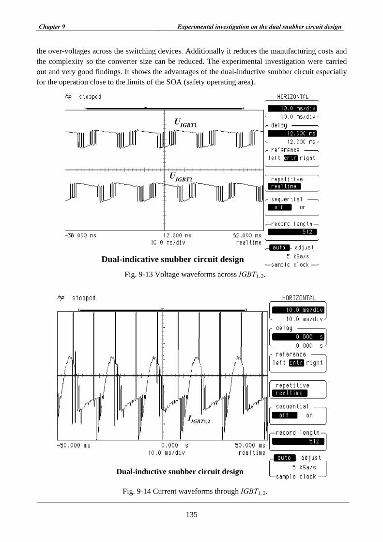
Chapter 9 Experimental investigation on the dual snubber circuit design
135
the over-voltages across the switching devices. Additionally it reduces the manufacturing costs and the complexity so the converter size can be reduced. The experimental investigation were carried out and very good findings. It shows the advantages of the dual-inductive snubber circuit especially for the operation close to the limits of the SOA (safety operating area).
UIGBT1
UIGBT2
Dual-indicative snubber circuit design
Fig. 9-13 Voltage waveforms across IGBT1, 2.
IIGBT1,2
Dual-inductive snubber circuit design
Fig. 9-14 Current waveforms through IGBT1, 2.

Chapter 9 Experimental investigation on the dual snubber circuit design
136
Dual-indicative snubber circuit design
UDS1
UON1
Fig. 9-15 Voltage waveforms across DS1, DON1.
UL
IL
Dual-indicative snubber circuit design
Fig. 9-16 Load voltage- and current-waveforms.

Chapter 10 Conclusion
137
10 Conclusion
In this work new and simple snubber circuits for three-level inverter system were proposed and suggested, which have several new features. These suggested circuits were tested by using a Matlab®/SimulinkTM Simulation which was based on a single phase model of a MV three level inverter system. The overvoltages and the losses are compared between the conventional and the other suggested snubber circuit configurations: the double snubber circuit, the optimized snubber circuit design, the dual-use snubber circuit and the dual-inductive snubber circuit. The results clarify the advantages of the proposed designs especially for the operation close to the limits of the SOA (Safety Operating Area) as in the following:
• The double snubber circuit, which is suitable for high voltage and high power more level converter systems and FACTS devices, has the advantages of both the RC and RCD snubber circuit. This means, the facility to minimize both, the over voltage and the losses in the entire circuit. Therefore the additional RC circuit can compensate the disadvantage of the conventional RCD snubber design, that the effective value for RS during the charging of the snubber capacity CS is essentially zero. But still the number of the total snubber circuit elements is large, so the total losses will be bigger compared ti the following snubber circuit designs.
• The optimized snubber design is proposed to be used in high voltage and high power more level converter systems and partially FACTS devices. The optimized snubber design is based on a new and simple structured snubber, which depends on passive elements. As a result, the number of required components is reduced, and the reliability increases distinctly. The presented optimized snubber design provides several additional advantages: It increases the optional performance of the three level converters due to the lower clamping over-voltages across the switching devices, it improves the efficiency because of the lower snubber- and total losses, its suitable structure can be extended to energy recovery snubbers and there is no unbalancing problem. Additionally, the manufacturing costs, the complexity and therefore the converter size can be reduced.
• The dual-use snubber design has the same advantages of the optimized snubber design; and more than that: the new position of turn-off snubber resistor RS which has two new functions the first is during the discharge process of CS1, and the second is during the charging process of CS2. So the resistor has a damping effect of the over-voltage across the power switching device while charging process of CS2, this means that the over-voltage will be reduced, especially in the beginning of turn-off process.
• The dual-inductive snubber design is also expedient for using in high- voltage and power level converter systems and a FACTS devices. The dual-inductive snubber design has the same structure und advantages of the dual-use snubber circuit. But the added inductance suppresses the over-voltage across the switching device more effectively and improves the efficiency due to minimize the losses.
In the experimental part of the dissertation, the dual-use and dual-inductive snubber circuits of three-level inverter systems were tested. The investigation results show that:
• The dual-use snubber circuit has perfectly reduced the over-voltage across the IGBTs, restricted the current changing, and suppressed the over-voltages across the snubber circuit diodes. The results were compatible with those of the simulation results in Matlab®/SimulinkTM.
• The dual-inductive snubber circuit tests were carried out and also the results correspond to the simulation results of the Matlab®/SimulinkTM studies. The added inductive in the turn on snubber circuit absorbs a big part of the current while a small part will flow through the

Chapter 10 Conclusion
138
turn on snubber circuit resistor which causes the over-voltage. The value of the measured current through the resistor was about 10% of the total current of the turn on snubber circuit. The shape of the load voltages and currents were much better than in the dual-use snubber circuit. So, the dual-inductive snubber design will improve the total efficiency due to the mentioned features.

Chapter 11 Zusammenfassung
139
11 Zusammenfassung
In der vorliegenden Arbeit werden Schutzbeschaltungen für Dreipunkt-Zwischenkreisstromrichter entwickelt und vorgeschlagen, die neuartige Möglichkeiten beinhalten. Die vorgeschlagenen Schaltungen wurden mit Matlab®/SimulinkTM Modellen entwickelt und überprüft. Verwendet wurde ein einphasiges Modell eines Dreipunktumrichters für Mittelspannungsanwendungen. Die Überspannungen und die Verluste werden zwischen der konventionellen und den hier vorgeschlagen Schutzbeschaltungen verglichen: der Doppelschutzbeschaltung oder auch „Double Snubber Circuit“, der optimierten Schutzbeschaltung, oder „Optimized Snubber Circuit Design“, der Mehrzweckschutzbeschaltung oder „Dual-use Snubber Circuit“ und der Doppel-induktiv Schutzbeschaltung oder „Dual-inductive Snubber Circuit“. Die Resultate erklären die Vorteile der vorgeschlagenen Entwürfe besonders für den Betrieb nahe der Grenze der SOA (Sicherer Arbeitsbereich) wie folgt:
• Der „Double Snubber Circuit“, der für Hochspannungsanwendungen und mehrstufige Umrichtersysteme für FACTS-Anlagen zweckmäßig ist, vereint die Vorteile der RC und RCD Schutzbeschaltungen. Die zusätzliche RC Schutzbeschaltung kann den Nachteil der konventionellen RCD Schutzbeschaltung ausgleichen, so dass der wirkungsvolle Wert von RS während der Aufladung des Schutzbeschaltungskondensators CS naher Null ist. Jedoch ist die Zahl der Beschaltungselemente groß, und somit sind die Gesamtverluste größer als bei den andren vorgeschlagenen Schutzbeschaltungsentwürfen.
• Die vorgeschlagene optimierte Schutzbeschaltung oder „Optimized Snubber Circuit“ kann in mehr stufige Hochspannungs- und Hochleistungsstromrichtern und teilweise in FACTS-Anlagen verwendet werden. Der optimierte Schutzbeschaltungsentwurf basiert auf einer neuen und einfacher strukturierten Schutzbeschaltung, insbesondre bezügliche der passiven Elemente. Als Ergebnis, wird die Zahl der erforderlichen Bauteile verringert und die Zuverlässigkeit wird deutlich erhöht. Der dargestellte optimierte Schutzbeschaltungsentwurf gewährt mehrere zusätzliche Vorteile: Er erhöht die Leistungsfähigkeit des Dreipunkt-Zwischenkreisstromrichters wegen der niedrigeren Überspannungen über dem Leistungshalbleiter, verbessert die Leistungsfähigkeit, wegen der geringeren Schutzbeschaltung und die Gesamtverluste. Die verwendete Struktur kann zu einer Schutzbeschaltung mit Energierückgewinnung erweitert werden und es gibt keine Probleme bzgl. einer unsymmetrischen Spannungsaufteilung. Zusätzlich können die Herstellungskosten, die Komplexität und damit die Konvertergröße verkleinert werden.
• Der zweifache Schutzbeschaltungsentwurf oder „Dual-use snubber circuit“ hat neben denVorteilen des optimierten Schutzbeschaltungsentwurfs weitere: die neue Position des Abschaltschutzwiderstandes RS, besitzt zwei neue Funktionen. Die Einerseits während des Entladungsprozesses von CS1 und andererseits während des Aufladungsprozesses von CS2. Der Widerstand hat einen Dämpfungseffekt bezüglich der Überspannungen über den Leistungshalbleitern während der Aufladung von CS2. Dies gilt insbesondere für den Beginn des Abschaltprozesses.
• Die Doppel-induktive Schutzbeschaltung oder „Dual-inductive Snubber Circuit“ ist ebenfalls für die Verwendung in mehrstufigen Hochspannungs- und Hochleistungsstromrichtersystemen und FACTS-Anlagen geeignet. Die doppel-induktive Schutzbeschaltung hat in wesentlichen die Struktur und die Vorteile des zweifachen Schutzbeschaltungsentwurfs. Jedoch unterdrückt die zusätzliche Induktivität die
Chapter 11 Zusammenfassung
140
Überspannungen über den Leistungshalbleitern noch stärker und verbessert die Leistungsfähigkeit durch eine Minimierung der Gesamtverluste.
Im experimentellen Teil der Dissertation, wurden die zweifache- und die doppel-induktive Schutzbeschaltung der Dreipunktstromrichtersysteme überprüft. Die Resultate zeigen:
• Die zweifache Schutzbeschaltung konnte die Überspannungen über den IGBTs in sehr guter Weise verringern, die Flankensteilheit des Stromes wird begrenzt und die Überspannungen über den Schutzbeschaltungsdioden unterdrückt. Die Resultate stimmen mit denen der Simulation in Matlab®/SimulinkTM
überein.
• Bei der doppelinduktiven Schutzbeschaltung entsprechen die Messergebnisse den Simulationsergebnissen mit Matlab®/SimulinkTM. Die zusätzliche Induktivität in der Einschaltschutzbeschaltung nimmt einen großen Teil des Stromes auf, während ein kleiner Teil den Einschaltwiderstand durchfließt. Die Spannungs- und Stromform bezüglich der Last konnte gegenüber der zweifachen Schutzbeschaltung weiter verbessert werden. Somit optimiert die doppel-induktive Schutzbeschaltung die Gesamt-Leistungsfähigkeit des Stromrichtersystems weiter.

Appendix A1 Abbreviation and symbols
141
Appendix A1 Abbreviations and symbols
INom : Forward conduction mode. VD-Nom : Forward blocking mode. VR-Nom : Reverse blocking mode. t1 : Needed time for junction biased reverse. t2 : Charge storage time in the bulk semiconductor material. trr : Reverse recovery time. Irr : Reverse recovery current. IRR : Peak reverse recovery current. Qrr : Reverse recovery charge. VF : Diode forward voltage drop. ICE : Collector-Emitter current. IC : Collector current. VCE : Collector-Emitter voltage. VGE : Gate-Emitter voltage td(on) : Turn-on delay time. tr : Rise time. td(off) : Turn-off delay time. tf : Fall time. VGET : Threshold voltage of the Gate-Emitter voltage. SCR : Silicon Controlled Rectifier. IG : Gate current. td : Delay time. IT : Full anode conducting current. IRM : Maximum reverse-recovery current. VRRM : Maximum reverse-recovery voltage. VAK : Anode-Cathode voltage. tq : Turn-off time of the Thyristor. Tj : The temperature of the junction. IT : Thyristor current. VR : Reverse recovery voltage. VDRM : Peak Off-state voltage. VG : Gate voltage. rv : Radii of GTO wafer. Vd : DC voltage. FACTS : Flexible AC Transmission Systems.

Appendix A1 Abbreviation and symbols
142
Vo : Output voltage. io : Output current. VS : DC voltage. Id : Supply DC current.
δ : Phase angle (pulse width).
Von : The rms value of the nth order AC output voltage. Vo1 : The rms fundamental output voltage. eC : Maximum value of the sinusoidal modulating voltage. fo : Output frequency. vtri : Saw-wave voltage. vtri,max : Maximum value of the saw-wave voltage. Vo1max : Fundamental output voltage. vABC : Line-line voltages. VAN: : Line-neutral voltage for phase A. vl-N : Line-neutral voltage. mf : Frequency modulation ratio. Vmax : Peak value of the input AC voltage.
Lσ : Stray inductance.
IO : Load current. RS : Snubber resistor. CS : Snubber capacitor.
SCv : Snubber capacitor voltage.
ω : Angular frequency.
Irr : Reverse recovery current. Cbase : Baseline capacitor.
,maxSCv : Maximum value of the snubber capacitor voltage.
fDv : Free-wheel diode voltage.
Rbase : Baseline snubber resistor. Ropt : Optimum value of the snubber resistor. WR : Energy loss in RS
SCW : Energy stored in CS.
Wtot : Total energy dissipated in the diode and its snubber resistor. xC : Line impedance. VLL : Line-to-line voltage. Id : Load current. Wsnubber : Total energy loss in the snubber circuit.

Appendix A1 Abbreviation and symbols
143
Psnubber : Total power loss in the snubber circuit.
SCi : Charging current of the snubber capacitor.
tfi : Current fall time. ton state : Turn-on time FBSOA : Forward biased safe operation area. RBSOA : Reverse biased safe operating area
∆VCE : Over-voltage across the transistor.
VCE,max : The maximum over-voltage across the transistor. COV : Over-voltage capacitor. ROV : Over-voltage resistor. k : Constant factor. tri : Current rise time.
Cτ : Time constant of the turn-off snubber circuit.
toff state : Turn-off time.
SLR : The resistor of the turn-on inductance.
τL : Time constant of the turn-on snubber circuit.
VCESP : Turn off surge voltage peak. VFM : Transient forward voltage drops in the snubber diode. VCEP : Snubber capacitor peak voltage. f : Switching frequency. P : Power dissipation caused by the snubber resistor.
σ : On time (Pulse width duration per half cycle for ON period).
α : Off time. (Pulse width duration per half cycle for Off period) V1max : Maximum value of the fundamental voltage V1. SOA : Safe Operating Area. CP : Parallel snubber capacitor. RP : Parallel snubber resistor.

Appendix A2 List of Figures
144
Appendix A2 List of Figures
Fig.3-1 Device operational states for (a) symmetrical device and (b) asymmetrical device. ..............7 Fig.3-2 Diode: (a) diode symbol, (b) diode structure, and (c) more detailed diode structure. ..........11 Fig.3-3 (a) Diode forward- and (b) reverse-recovery-biased.............................................................11 Fig.3-4 Diode characteristics. ............................................................................................................13 (a).Input waveform applied to the diode in Fig.3-3(a), (b) The excess-carrier density at the junction, (c) The diode current, (d) The diode voltage, (e) Diode reverse-recovery characteristics. ...............13 Fig.3-5 IGBT transistor: (a) IGBT transistor structure and the location of the equivalent circuit, (b) the equivalent circuit, (c) IGBT symbol. ...........................................................................................14 Fig.3-6 IGBT current-voltage (IC-VGE) characteristics for a given value of VCE. ..............................15 Fig.3-7 Switching characteristic of an IGBT. ....................................................................................16 Fig.3-8 Thyristor (a) Thyristor symbol, (b) Thyristor structure, (d) two-transistor structure, and (d) Thyristor equivalent circuit................................................................................................................18 Fig.3-9 Switching characteristics of the thyristor. .............................................................................19 Fig.3-10 Gate turn-off thyristor (a) GTO -symbol, (b) -structure and (c) -equivalent circuit. ..........21 Fig.3-11 (a) A picture of GTO surface (b) A picture of GTO wafer including definition of radii rv.21 Fig.3-12 GTO turn-on and turn-off process: (a) turn-on and (b) turn-off..........................................23 Fig.3-13 Conduction and conventional Turn-off of a GTO...............................................................24 Fig.3-14 MOS Turn-off (MTO) thyristor (a) MTO symbol, (b) MTO structure; (c) MTO equivalent circuit, and (d) more detailed equivalent circuit. ...............................................................................25 Fig.3-15 Emitter Turn-off (ETO) thyristor: (a) ETO symbol, (b) ETO equivalent circuit, and (c) ETO structure.....................................................................................................................................25 Fig.3-16 IGCT thyristor (a) IGCT symbol (b) IGCT structure with a Gate-Commutated Thyristor and reverse diode. ..............................................................................................................................26 Fig.3-17 MOS-Controlled Thyristor (MCT) (a) MCT symbol, (b) MCT structure (c) MCT equivalent circuit................................................................................................................................27 Fig.3-18 Control characteristics of power switching devices. ...........................................................28 Fig.4-1 Basic types of FACTS Controllers (a) general symbol for FACTS controller; (b) series controller; (c) shunt controller; (d) unified series-series controller; (e) coordinated series and shunt controller; (f) unified series-shunt controller; (g) unified controller for multiple lines; (h) series controller with storage; (i) shunt controller with storage; (j) unified series-shunt controller with storage. ...............................................................................................................................................32 Fig.4- 2 Shunt-connected Controllers (a) Static Synchronous Compensator (STATCOM) based on voltage-sourced and current-sourced converter; (b) STATCOM with storage, i.e., Battery Energy Storage System (BESS), Superconducting Magnet Energy System and large capacitor; (c) Static VAR Compensator (SVC); (d) Static VAR Generator (SVG), Static VAR System, Thyristor-Controlled Reactor (TCR), Thyristor-Switched Capacitor (TSC), and Thyristor-Switched Reactor (TSC); (d) Thyristor-Controlled Braking Resistor.............................................................................35 Fig.4-3 (a) Static Synchronous Compensator (SSSC) (b) SSSC with storage; (c) Thyristor-Controlled Series Capacitor (TCSC) and Thyristor Switched Series Capacitor (TSSC), and (d) Thyristor-Controlled Series Reactance (TCSR) and Thyristor-Switched Series Reactance. ............39 Fig.4-4 (a) Thyristor-Controlled Phase-Shifting Transformer (TCPST) or Thyristor-Controlled Phase Angle Regulator (TCPR); (b) Unified Power Flow Controller (UPFC)..................................41 Fig.4- 5 Various other controllers (a) Thyristor-Controlled Voltage Limiter (TCVL), (b) Thyristor-Controlled Voltage Regulator (TCVR) based on tap changer, (c) Thyristor-Controlled Voltage Regulator (TCVR) based on voltage injection...................................................................................41 Fig.5-1 Basic principle of Voltage-Sourced Converter: (a) Valve for a Voltage-Sourced Converter; (b) Voltage-Sourced Converter concept; (c) Single-valve operation.................................................44 Fig.5-2 Single-phase half-bridge converter. ......................................................................................45

Appendix A2 List of Figures
145
Fig.5-3 Single-phase full-bridge converter with RL-load..................................................................46 Fig.5-4 The regulation of the output voltage by means of a phase-controlled. .................................47 Fig.5-5 The regulation of the output voltage by means of a DC-DC converter. ...............................47 Fig.5-6 The waveform of the output voltage of Full-bridge converter. .............................................48 Fig.5-7 Three-phase full-wave bridge converter................................................................................49 Fig.5-8 The switching scheme of three-phase Voltage-Sourced Converter. .....................................50 Fig.5-9 The switching scheme for three-phase VSC 120° conducting stead of 180°........................51 Fig.5-10 One phase-leg of a three-level converter.............................................................................52 Fig.5-11 Operation of thee-level converter, output AC voltage. .......................................................53 Fig.5-12 Operation of a PWM converter with switching frequency of three times the fundamental frequency............................................................................................................................................54 Fig.6-1 Voltage-sourced and Current-Sourced Converter concepts: (a) voltage sourced converter; (b) Current-Sourced Converter. .........................................................................................................55 Fig.6-2 Types of Current-Sourced Converter, (a) diode rectifier; (b) Thyristor line-commutated converter, (c) self-commutated converter. .........................................................................................56 Fig.6-3 Diode bridge rectifier. ...........................................................................................................58 Fig.6-4 A three-phase bridge rectifier................................................................................................58 Fig.6-5 The rectifier and the phase controller for a half-wave converter. .........................................59 Fig.6-6 A single-phase fully-controlled bridge rectifier (thyristor with p=2). ..................................60 Fig.6-7 Three-phase, fully-controlled bridge converter circuit..........................................................60 Fig.6-8 Self-commutating current-sourced converter: (a) six-pulse converter, (b) commutation process, (c) current waveforms, and (d) system interface..................................................................62 Fig.7-1 (a) A step-down converter circuit with stray inductance and a snubber circuit for the free-wheel diode, (b) the Diode reverse-recovery current and diode voltage. ..........................................65 Fig.7-2:(a) Equivalent circuit of the step-down converter at the instant of diode reverse-recovery current snap-off (b) the simplification that results when the snubber resistance is zero and (c) The voltage and current waveforms for RS = 0 and CS = Cbase..................................................................67 Fig.7-3 Equivalent circuit with snubber resistance RS. ......................................................................67 Fig.7-4 The current and the voltage waveforms after diode snaps-off at t = 0..................................68 Fig.7-5 Maximum over-voltage across the diode as a function of the snubber resistance for a fixed value of the snubber capacitance. ......................................................................................................69 Fig.7-6 Snubber energy loss and the maximum diode voltage for the optimum value of the snubber resistance RS as a function of the snubber capacitance CS ................................................................69 Fig.7-7 Turn-off snubbers for Thyristors in a three-phase line-frequency converter circuit: (a) three-phase line-frequency converter, (b) trigger time, and (c) the equivalent circuit................................71 Fig.7-8 (a) A step-down converter circuit with stray inductance shown explicitly with (b) associated switching trajectory and (c) the current and voltage waveforms during turn-on and turn-off...........72 Fig.7-9 (a) turn-off snubber circuit, (b) its equivalent circuit during the transient and (c) current and voltage waveforms during the turn-off transient. (The shaded areas in Fig.7-9 (c) represent the charge put on the snubber capacitance during turn-off that will be dissipated in the power switching device at the next turn-off.)................................................................................................................74 Fig.7-10 Switching trajectory during turn-off with various values of snubber capacitance CS.........75 Fig.7-11 Effect of the snubber capacitance CS on the turn-off transient without (a) snubber resistance RS and (b) with the resistance............................................................................................76 Fig.7-12 Turn-off energy dissipation in the power switching device and the snubber resistance RS as a function of the snubber capacitance CS. ..........................................................................................77 Fig.7-13 (a) Over-voltage snubber, (c, b) its equivalent circuit during transient turn-off, (d) the collector-emitter voltage with and without the snubber.....................................................................78 Fig.7-14 Turn-on snubber circuit (a) in series with the power switching device or (b) in series with the free-wheel diode, (c) The power switching device voltage and current waveforms for small value of Lσ and (d) for Large values of Lσ. ........................................................................................80
Appendix A2 List of Figures
146
Fig.7-15 A modified circuit with an over-voltage snubber, a turn-on snubber, and turn-off snubber; the Undeland snubber for step-down converter. ................................................................................81 Fig.7-16 Step-down converter circuit using a GTO as the switching device with turn-on and turn-off snubbers .............................................................................................................................................82 Fig.7-17 Test chopper circuit. ............................................................................................................83 Fig.7-18 IGBT Switching waveforms during the turn-off and turn-on processes .............................84 Fig.7-19 Schematic type of individual snubber circuits: (a) RC snubber circuit, (b) Charge discharge RCD snubber circuit, (c) Discharge suppressing RCD snubber circuit, (d) C snubber circuit and (e) RCD snubber circuit...........................................................................................................................86 Fig.7-20 Turn-off locus waveform of IGBT......................................................................................87 Fig.7-21 Voltage and current waveforms at turn-off. IGBT..............................................................87 Fig.8-1 Single phase of a three level converter (common snubber circuit). ......................................90 Fig.8-2 Proposed double snubber circuit configuration in a three level inverter system...................91 Fig.8-3 An optimized snubber design for Single phase three level GTO inverters. ..........................92 Fig.8-4 Commutation path of the transition form S0 to S1: (a) initial state, (b) phase 1 and (c) phase-2..........................................................................................................................................................94 Fig.8-5. Commutation path of the transition form S1 to S0: (a) initial state, (b) phase 1 and (c) phase-2..........................................................................................................................................................95 Fig.8-6 Commutation path of the transition form S0 to S-1: (a) initial state, (b) phase 1 and (c) phase-2..........................................................................................................................................................96 Fig.8-7 One phase of a three level inverter with the new dual-use snubber circuit design. ..............98 Fig.8-8 One phase of a three-level inverter with the new dual-inductive snubber circuit. ................99 Fig.8-9 The main flow chart of the PWM in Matlab®/SimulinkTM. ...............................................100 Fig.8-10 The internal part of the PWM in Matlab®/SimulinkTM. ...................................................101 Fig.8-11 The comparison functions of the PWM in Matlab®/SimulinkTM. ....................................101 Fig.8-12 the output of the PWM in Matlab®/SimulinkTM...............................................................102 Fig.8-13 The voltages on GTO1 and GTO2 in the common and the double snubber configuration (CP=0.05µF).....................................................................................................................................103 Fig.8-14 The currents in GTO1 and GTO2 in the common and the double snubber configuration (CP=0.05µF).....................................................................................................................................103 Fig.8-15 The currents in Df1 and Df2 in the common and the double snubber Configuration (CP=0.05µF).....................................................................................................................................104 Fig.8-16 The voltages on DS1 and DS2in the common and the double snubber configuration (CP=0.05µF).....................................................................................................................................104 Fig.8-17 The currents in DS1 and DS2 in the common and the double snubber configuration (CP=0.05µF).....................................................................................................................................105 Fig.8-18 The total losses (energy function) in RS1 in the conventional- and in RS1, RP1 in the proposed double snubber design over one cycle of the fundamental frequency (CP=0.05µF)........105 Fig.8-19 The voltages in GTO1 and GTO2 in the common and the double snubber configuration (CP=0.01µF).....................................................................................................................................106 Fig.8-20 The currents in GTO1 and GTO2 in the common and the double snubber configuration (CP=0.01µF).....................................................................................................................................106 Fig.8-21 The currents in DS1 and DS2 in the common and the double snubber configuration (CP=0.01µF).....................................................................................................................................107 Fig.8-22 The voltages on DS1 and DS2 in the common and the double snubber configuration (CP=0.01µF).....................................................................................................................................107 Fig.8-23 The currents in Df1and Df2 in the common and the double snubber Configuration (CP=0.01µF).....................................................................................................................................108 Fig.8-24 The total losses (energy function) in RS1 in the conventional and in RS1, RP1 in the proposed double snubber design over two cycles of the fundamental frequency (CP=0.01µF)......................108

Appendix A2 List of Figures
147
Fig.8-25 The voltages in GTO1 and GTO2 in the common and the optimized snubber design. ......109 Fig.8-26 The currents in GTO1 and GTO2in the common and the optimized snubber design.........110 Fig.8-27 (a) The currents in Df1 and Df2 and comparing the total losses in conventional and (b) the optimised snubber configuration (energy function).........................................................................110 Fig.8-28 The current in DS1 and Don1 in the common and the optimized snubber configuration. ...111 Fig.8-29 The voltages in DS1 and Don1 in the common and the optimized snubber configuration. .111 Fig.8-30 The voltages on GTO1 and GTO2 in the common and the optimized snubber design (CS=0.5µF, RS=5Ω)..........................................................................................................................112 Fig.8-31 The currents in GTO1 and GTO2 in the common and the optimized snubber design (CS=0.5µF, RS=5Ω)..........................................................................................................................112 Fig.8-32 Currents in DS1 and Don1 in the common and the optimized snubber configuration (CS=0.5µF, RS=5Ω)..........................................................................................................................113 Fig.8-33 Voltages on DS1 and Don1 in the common and the optimized snubber configuration (CS=0.5µF, RS=5Ω)..........................................................................................................................113 Fig.8-34 (a) The currents in Df2 and Df2 in the common and the optimized snubber configuration, and (b) the comparison of the total losses in the conventional and the optimized snubber configuration (energy function) (CS=0.5µF, RS=5Ω). .....................................................................114 Fig.8-35 The voltages in GTO1 and GTO2 in the common and the optimized snubber design (CS=0.25µF, RS=2Ω)........................................................................................................................115 Fig.8-36 The currents in GTO1 and GTO2 in the common and the optimized snubber design (CS=0.25µF, RS=2Ω)........................................................................................................................115 Fig.8-37 (a) The currents in Df2 and Df2 in the common and the optimized snubber configuration, and (b) the comparison of the total losses in the conventional and the optimized snubber configuration (energy function) (CS=0.25µF, RS=2Ω). ...................................................................116 Fig.8-38 The voltages on GTO1 and GTO2 in the common and the dual-use snubber configuration (CS-D=0.5µF, RS=2.5Ω). ...................................................................................................................117 Fig.8-39 The currents in GTO1 and GTO2 in the common and the dual-use snubber configuration (CS-D=0.5µF, RS=2.5Ω). ...................................................................................................................117 Fig.8-40 The currents in DS1 and Don1 in the common and the dual-use snubber configuration (CS-
D=0.5µF, RS=2.5Ω). .........................................................................................................................118 Fig.8-41 The voltages in DS1 and Don1 in the common and the dual-use snubber configuration (CS-
D=0.5µF, RS=2.5Ω). .........................................................................................................................118 Fig.8-42 (a) The currents in Df2 and Df2 in the common and dual-use snubber configuration, and (b) comparison of the total losses in the conventional and the optimized snubber configuration (energy function) (CS-D=0.5µF, RS=2.5Ω). ...................................................................................................119 Fig.8-43 The voltages in GTO1 and GTO2 in the common and the dual-use snubber configuration (CS-D=0.25µF, RS=2.5Ω). .................................................................................................................120 Fig.8-44 The currents in GTO1 and GTO2 in the common and the dual-use snubber configuration (CS-D=0.25µF, RS-D =2.5Ω)...............................................................................................................120 Fig.8-45 The voltages in DS1 and Don1 in the common and the dual-use snubber configuration (CS-
D=0.25µF, RS-D =2.5Ω).....................................................................................................................121 Fig.8-46 The voltages in DS1 and Don1 in the common and the dual-use snubber configuration (CS-
D=0.25µF, RS-D=2.5Ω). ....................................................................................................................121 Fig.8-47 (a) The currents in Df2 and Df2 in the common and dual-use snubber configuration and (b) comparison between the total losses in the conventional and the optimized snubber configuration (energy function) (CS-D=0.25µF, RS-D=2.5Ω). .................................................................................122 Fig.8-48 The voltages on GTO1 and GTO2 in the common and the Dual-indicative Snubber design (Ed=6000V, IL=5000A, CS=0.25µF, RS=2.5Ω). ...............................................................................123 Fig.8-49 The currents in GTO1 and GTO2 in the common and the Dual-indicative Snubber design (Ed=6000V, IL=5000A, CS=0.25µF, RS=2.5Ω). ...............................................................................123

Appendix A2 List of Figures
148
Fig.8-50 The voltages on DS1 and Don1 in the common and the Dual-indicative Snubber design (Ed=6000V, IL=5000A, CS=0.25µF, RS=2.5Ω). ...............................................................................124 Fig.8-51 The currents in DS1and Don1 in the common and the Dual-indicative Snubber design (Ed=6000V, IL=5000A, CS=0.25µF, RS=2.5Ω). ...............................................................................124 Fig.8-52 (a) The currents in Df2 and Df2 in the common and the Dual-indicative snubber design and (b) comparison of the total losses in the conventional and the optimized snubber configuration (energy function) (Ed=6000V, IL=5000A, CS=0.25µF, RS=2.5Ω). ..................................................125 Fig.9-1 Pulse scheme of Matlab®/SimulinkTM at 900Hz..................................................................126 Fig. 9-2: The schematic diagram of the driving circuit logic...........................................................127 Fig. 9-3: Functional simulation results from the ispDesignExpert. .................................................128 Fig. 9-4: The driving circuit including: (a) The 5 and 15 V power supply from a 12 V source (b) CPLD Chip and (c) 4 optocoupler ...................................................................................................128 Fig. 9-5 One period of the driving signals .......................................................................................128 Fig. 9-6: The logic block schematic diagram...................................................................................130 Fig. 9-7: Control block of the driving circuit...................................................................................130 Fig. 9-8 Control blocks of the complete Three-level IGBT inverter system. ..................................131 Fig. 9-9 Voltage waveforms across IGBT1, 2....................................................................................132 Fig. 9-10 Current waveforms through IGBT1, 2................................................................................133 Fig. 9-11 Voltage waveforms across DS1, DON1. ..............................................................................133 Fig. 9-12 Load voltage- and current-waveforms. ............................................................................134 Fig. 9-13 Voltage waveforms across IGBT1, 2..................................................................................135 Fig. 9-14 Current waveforms through IGBT1, 2................................................................................135 Fig. 9-15 Voltage waveforms across DS1, DON1. ..............................................................................136 Fig. 9-16 Load voltage- and current-waveforms. ............................................................................136

Appendix A3 List of Figures
149
Appendix A3 List of Tables
Table 1.1 the available diodes information’s. ....................................................................................12 Table 3.1 Switching signals for uni-polar single-phase converter.....................................................49 Table 8.1 the total number of snubber elements for the different snubber designs. . ........................91 Table 8.2 the total number of snubber elements for different snubber designs. ................................92 Table 8.3 the three Switching States..................................................................................................93 Table 8.4 the parameters of the used GTO and the load information................................................99 Table 8.5 Snubber circuits (common and double configuration) information.................................102 Table 8.6 the snubber circuits (common and design) information. .................................................109 Table 8.7 Snubber circuits (common and double dual-use) information.........................................116 Table 9.1 Dual-use- and dual-inductive snubber circuits information.............................................131

Appendix A4 References
150
Appendix A4 References [1] Alex Q. Huang, “Power Electronics Handbook-Power Semiconductor Devices,” 2003. [2] B.J. Baliga, “Power Semiconductor Devices,” PWS Publishing Company, 1994. [3] Narain G. Hingorani, Laszlo Gyugyi, Mohamed E. El-Hawary, “Concept and Technology of
Flexible AC Transmission Systems,” The Institute of Electrical and Electronic Engineering, Inc New York.
[4] M. Madhusudhan Rao, “Introduction to Power Electronics,” Indian 2005. [5] Stefan Schröder, Dirk Detjen, and Rik W. A. A. De Doncker, “Multi-cell Circuit Model for
High-Power Thyristor-Type Semiconductor Devices,” 0093-9994/03$17.00 © 2003 IEEE. [6] Kaushik Rajasheraka, Ashoka K. S. Bhat, Bimal K. Bose, “Power Electronics,” © 2000. [7] Zainal Salam, “Power Electronics and Derives”, UTM-JB 3-2003. [8] Ned Mohan, Tore M. Undeland, William P. Robins, Power electronic; second edition, John
Wiley & Sons Inc New York, USA, 1955. [9] Gregory Reed, Ronald Pape, Masatoshi Takeda “Advantages of Voltage Sourced Converter
(VSC) Based Design Concepts for FACTS and HVDC-Link Applications,” 0-7803-7990-X/03/$17.00C2003 IEEE
[10] F. Rahman, “DC-AC Converter (Inverter) Circuit (Part 1- Single-phase inverter),” ELEC4240/9240, “http://ee.unsw.edu.au/”.
[11] F. Rahman, “DC-AC Converter (Inverter) Circuit (Part 2- Three-Phase Inverter),” ELEC4240/9240, “http://ee.unsw.edu.au/”.
[12] F. Rahman, “Uncontrolled (diode) Rectifier Circuits,” ELEC4240/9240, “http://ee.unsw.edu.au/”.
[13] F. Rahman, “Phase-Controlled AC-DC Converters,” ELEC4240/9240, “http://ee.unsw.edu.au/”.
[14] W. McMurray “Optimum Snubber for Power Semiconductors,” IEEE Trans., vol. IA -8, no. 5, pp. 593-600, Sep/Oct.1970.
[15] Tore M. Undeland, A.Petteteic, G. Haukens, A. K. Adnanes, and S. Garberg, “A Diode and Thyristor Turn-off Snubber Simulation by KREAN and Easy-to-Use design Algorithm,” IEEE IAS Proc., 1988, pp. 647-654.
[16] W. McMurray “Selection of snubber and clamps to optimize the design of transistor switching converters ,” IEEE Trans. Ind. App., vol. IA -16, no. 4, pp. 513-523, July/Aug. 1980.
[17] E. T. Calkin and B. H. Hamilton, “Circuit technique for improving the switching loci of transistor Switches in Switching Regulators,” IEEE Trans. Indus. Appl. , vol. IA-12, no. 4 pp. 364-369, July/Aug. 1976.
[18] K. Harada, T. Ninomiya, and M. Kohno, “Optimum RC Snubber for Switching Regulator by means of the Root Locus Method,” in Conf. Rec. Power Electronics Specialists Conf., pp. 158-167.
[19] Tore M. Undeland, “Switching Stress Reduction in Power Transistor Inverter,” 1976 IEEE Industrial Applications Society Conference Proceeding, pp. 383-392.
[20] Tore M. Undeland, F. Jensen, A. Steinbakk, T. Rogne, and M. Hernes, “A Snubber Configuration for Both Power Transistor and GTO PWM Inverter,” IEEE Power Electronics Specialist Conf. REC., Gaithersberg, MD, June 18-21, 1984, pp. 42-53.
[21] Fuji IGBT Modules Application Manual, “Protection Circuit Design,” Fuji Electric Device Technology Co., Ltd. February 2004.
[22] Th. Schütze, “Design Aspects for Inverters with IGBT High Power Modules,” eupec GmbH & Co KG, Warstein, Germany.
[23] Rahul Chokhawala and Saed Sobhani, “Switching Voltage Transient Protection Schemes for High-current IGBT Modules,” IEEE Trans. Industry applications, vol. 31, no. 2, pp. 256-263, 1995.

Appendix A4 References
151
[24] Yi Zhang, Saed Sobhani, and Rahul Chokhawala, “Snubber Considerations for IGBT Application,” IPEMC, pp. 261-269, 1994.
[25] Tadashi Miyasaka and Shyuji Miyashita, “Protection of IGBT Modules in Inverter Circuits,” Power Conversion, pp. 211-216, 1991.
[26] J. B. Rice, “Design of Snubber Circuits for Power Semiconductors,” IEEE Conf. Rec. of fourth Annual Meeting of Industry and General Applications Group, pp- 485-489, 1969.
[27] Jea-Hyeong Suh, Bum-Seok Suh, and Dong-Seok Hyun, “A New Snubber Circuit for High Efficiency and Over-voltage Limitation in Three-Level GTO Inverters,” IEEE Trans. On Industrial Electronics, Vol. 44, No. 2, April 1997, pp: 145-156.
[28] Jeong-Hyoun Sung, “A Simple Snubber Configuration for Three-Level GTO Inverters,” 0885-8993/99/$10.00 ©1999 IEEE.
[29] T. M. Undeland, “Snubber for Pulse Width Modulated Bridge Converters with Power Transistors and GTO’s,” Conf. Rec. Int. Power Electronic Conf., 1983, pp. 313-323.
[30] Joonmi OH, Jinhwang Jung and Kwanghee Nam,” A Simple Snubber Configuration for Three Level Voltage Source GTO Inverters,” 0-7803-3008-0/95$4.00 ©1995 IEEE.
[31] W. McMurray “Efficient Snubbers for Voltage-Source Inverters,” IEEE Trans., Power Electronics”. Vol. PE-2, no 3, pp 264-274 July 1987.
[32] William P. Robbins, “Snubber Circuits,” Snubbers-1 © 1997. [33] Severns R. “Design of Snubber for Power Circuit,” Cornell Dubilier cooperation. [34] In-Dong Kim, Eui-Cheol Nho and Bimal K. Bose “A Snubber Circuit for Multilevel Inverter
and Converter,” 07803-4943-1/98/$10.00 ©1998 IEEE. [35] Steven C. Rizzo, Bin Wu, and Reza Sotudeh, “Symmetric GTO and Snubber Component
Characterization in PWM Current-Source Inverters,” 0885-8993/98$10.00 ©1998 IEEE. [36] J: Alnasseir, Ch. Weindl, G. Herold, “Calculation of Over-voltage and Losses in Three Level
Converters with Double Snubber Circuit,” EPE-PEMC 2004, 11th International Power Electronic and Motion Control Conference, Sep, 2-4 Riga, Latvia 2004.
[37] H. Levy, I. Zafrany, G. Ivensky and S. Ben-Yaakov, “Analysis and Evolution of A Lossless Turn-on Snubber,” in IEEE APEC Conf. Rec., 1997, pp. 757-763.
[38] L. Eriksson, J. Donlon, and R. Chokhawala, “Assignment of Turn-on and Turn-off Power and Energy Losses in GTO,” in IEEE IAS Ann. Meet., 1989, pp. 1286-1285.
[39] A. Brambilla and E. Dallago, “Snubber Circuit and Losses of Voltage Source GTO Inverters,” IEEE Trans. Power Electronic, vol. PE-7, pp. 231-240, Jan 1992.
[40] Zach, Kaiser, Kolar and Haselstein, “New Lossless Turn-on and Turn-off (Snubber) Networks for Inverters, Including Circuit for Blocking Voltage Limitation,” IEEE Transaction on Power Electronics, vol. PE-1, no. 2, April 1986, pp. 65-75.
[41] J. Holtz, S. Salama, and K.H. Werner, “A Non-dissipative Snubber Circuit for High Power GTO Inverters,” IEEE Trans. Ind. Applicat, vol. 25, no. 4, pp. 620-626, July/Aug 1989.
[42] A. Brambilla and E. Dallago, A. Coffetti, U. Mauri, and R. Romano, “Analyses of Snubber Circuit of GTO Power Converter for Electrical Traction,” (in Italian) L’Energia Elettrica, no. 6 June 1990, pp. 263-272.
[43] Jim Hagerman, “Calculating Optimum Snubbers,” Hagerman Technology, 12 Dec. 1994. [44] J. H. Suh, B. S Suh, and D. S. Hyun, “A New Snubber Circuit for High Efficiency and Over-
voltage Limitation in Three Level GTO Inverters,” IEEE Trans. Ind. Applicat, vol. 44, no. 2, pp. 145-156, 1997.
[45] Chang Woo Lee and Song Bei Park, “Design of a Thyristor Snubber Circuit by Considering the Reverse Recovery Process,” 0885-8993/88/1000-0440$01.00 ©1988 IEEE.
[46] S. Irokawa, T. Kitahara, F. Kchikawa, and T. Nakajima, “A New Snubber Energy Recovery Method for Voltage Source Self Commutated Converters,” IPEC-Yokohama ’95, pp 1572-1577.
[47] Lesnicar, and R. Marquardt, “An Innovative Modular Multilevel Converter Topology Suitable for a Wide Power Range,” 0-7803-7967-5/03/$17.00 © 2003 IEEE.

Appendix A4 References
152
[48] K.B. Hughes, C. D. Schauder, M. G. Gernhardt, E. J. Stacey, “Effect of Snubber Circuit Parameters on the Turn-off Voltage Spike of Large GTO Thyristors,” 07803-1462-x/93$03.00 ©1993 IEEE.
[49] R. Basset and C. Smith, “Power Losses in GTO Switching Applications,” PCIM-Europe, Power Conversion & Intelligent Motion, Sept. 1989, pp. 192-197.
[50] J: Alnasseir, Ch: Weindl, G: Herold, “An Optimized Snubber Design for Three Level Inverter Systems,” EPE2005, 11th European Conference on Power Electronics and Application, Sep, 11th-14th, 2005, Dresden, Germany.
[51] Fang Z. Peng, Gui-Jia Su, and Leon M. Tolbert, “A Passive Soft Switching Snubber for PWM Inverters,” IEEE Trans. On Power Electronics, vol. 19, no. 2, March 2004.
[52] Domb, M., “Non-dissipative Turn-off Snubber Alleviates Switching Power Dissipation, Second-Breakdown Stress and VCE Overshoot”, IEEE PESC proceedings, 1982, pp. 445-454.
[53] Song Qiang, Liu Wenhau, Wang Zhiyoung, Chen XiZheng, and Xu Peifeng, “Design of Snubber Circuit for The 4500V/4000A GTO’s in a 20MVA STATCOM,” IPEMC 2000, third International Power Electronic and Motion Control Conference, Aug 15-18, 2000 Beijing, Chine.
[54] B. S. Suh and D. S. Hyun, “A Circuit Design for Clamping and Over-voltage in Three Level GTO Inverters,” in IECON ’94, pp. 651-656
[55] Hansen, A., Hanemann, H. “Design of Snubber Circuits for Transistor-Inverter using Minimum Number of Components,” Conference Proceedings IFAC 1983, pp. 165-171.
[56] H. Ohashi, “Snubber Circuit for High-Power Gate Turn-off Thyristors,” IEEE Trans. Ind. App., vol. IA -19, no. 4, pp. 655-664, July/Aug. 1983.
[57] J. Alnasseir, Ch. Weindl, G. Herold, “A Dual-use Snubber Design for Multi-Level Inverter Systems,” EPE-PEMC 2006, 12th International Power Electronics and Motion Control Conference, Aug 30-Sep 1, 2006, Portoroz, Slovenian.